US20090301562A1 - High efficiency photovoltaic cell and manufacturing method - Google Patents
High efficiency photovoltaic cell and manufacturing methodDownload PDFInfo
- Publication number
- US20090301562A1 US20090301562A1US12/475,858US47585809AUS2009301562A1US 20090301562 A1US20090301562 A1US 20090301562A1US 47585809 AUS47585809 AUS 47585809AUS 2009301562 A1US2009301562 A1US 2009301562A1
- Authority
- US
- United States
- Prior art keywords
- copper
- indium
- forming
- layer
- copper indium
- Prior art date
- Legal status (The legal status is an assumption and is not a legal conclusion. Google has not performed a legal analysis and makes no representation as to the accuracy of the status listed.)
- Abandoned
Links
- 238000004519manufacturing processMethods0.000titledescription7
- 238000000034methodMethods0.000claimsabstractdescription137
- 239000000463materialSubstances0.000claimsabstractdescription107
- HVMJUDPAXRRVQO-UHFFFAOYSA-Ncopper indiumChemical compound[Cu].[In]HVMJUDPAXRRVQO-UHFFFAOYSA-N0.000claimsabstractdescription82
- BWGNESOTFCXPMA-UHFFFAOYSA-NDihydrogen disulfideChemical compoundSSBWGNESOTFCXPMA-UHFFFAOYSA-N0.000claimsabstractdescription72
- 239000010949copperSubstances0.000claimsabstractdescription65
- 239000010409thin filmSubstances0.000claimsabstractdescription48
- 239000000758substrateSubstances0.000claimsabstractdescription26
- NINIDFKCEFEMDL-UHFFFAOYSA-NSulfurChemical group[S]NINIDFKCEFEMDL-UHFFFAOYSA-N0.000claimsabstractdescription20
- 239000011593sulfurSubstances0.000claimsabstractdescription20
- 229910052717sulfurInorganic materials0.000claimsabstractdescription20
- 238000007669thermal treatmentMethods0.000claimsabstractdescription17
- 238000004544sputter depositionMethods0.000claimsabstractdescription10
- 229910052738indiumInorganic materials0.000claimsdescription43
- RYGMFSIKBFXOCR-UHFFFAOYSA-NCopperChemical compound[Cu]RYGMFSIKBFXOCR-UHFFFAOYSA-N0.000claimsdescription41
- 229910052802copperInorganic materials0.000claimsdescription40
- APFVFJFRJDLVQX-UHFFFAOYSA-Nindium atomChemical compound[In]APFVFJFRJDLVQX-UHFFFAOYSA-N0.000claimsdescription39
- 239000006096absorbing agentSubstances0.000claimsdescription18
- OMZSGWSJDCOLKM-UHFFFAOYSA-Ncopper(II) sulfideChemical compound[S-2].[Cu+2]OMZSGWSJDCOLKM-UHFFFAOYSA-N0.000claimsdescription15
- 239000004065semiconductorSubstances0.000claimsdescription15
- XLOMVQKBTHCTTD-UHFFFAOYSA-NZinc monoxideChemical compound[Zn]=OXLOMVQKBTHCTTD-UHFFFAOYSA-N0.000claimsdescription13
- 230000015572biosynthetic processEffects0.000claimsdescription12
- NNFCIKHAZHQZJG-UHFFFAOYSA-Npotassium cyanideChemical compound[K+].N#[C-]NNFCIKHAZHQZJG-UHFFFAOYSA-N0.000claimsdescription10
- 239000011787zinc oxideSubstances0.000claimsdescription6
- WUPHOULIZUERAE-UHFFFAOYSA-N3-(oxolan-2-yl)propanoic acidChemical compoundOC(=O)CCC1CCCO1WUPHOULIZUERAE-UHFFFAOYSA-N0.000claimsdescription5
- RWSOTUBLDIXVET-UHFFFAOYSA-NDihydrogen sulfideChemical compoundSRWSOTUBLDIXVET-UHFFFAOYSA-N0.000claimsdescription5
- 239000005083Zinc sulfideSubstances0.000claimsdescription5
- 229910052980cadmium sulfideInorganic materials0.000claimsdescription5
- 238000006243chemical reactionMethods0.000claimsdescription5
- 229910000037hydrogen sulfideInorganic materials0.000claimsdescription5
- 229910052984zinc sulfideInorganic materials0.000claimsdescription5
- HCHKCACWOHOZIP-UHFFFAOYSA-NZincChemical compound[Zn]HCHKCACWOHOZIP-UHFFFAOYSA-N0.000claimsdescription4
- PNHVEGMHOXTHMW-UHFFFAOYSA-Nmagnesium;zinc;oxygen(2-)Chemical compound[O-2].[O-2].[Mg+2].[Zn+2]PNHVEGMHOXTHMW-UHFFFAOYSA-N0.000claimsdescription4
- 239000013077target materialSubstances0.000claimsdescription4
- 229910052725zincInorganic materials0.000claimsdescription4
- 239000011701zincSubstances0.000claimsdescription4
- DRDVZXDWVBGGMH-UHFFFAOYSA-Nzinc;sulfideChemical compound[S-2].[Zn+2]DRDVZXDWVBGGMH-UHFFFAOYSA-N0.000claimsdescription4
- GXAAOYDOGKQENU-UHFFFAOYSA-N[Al+3].[S--].[S--].[Cu++].[In+3]Chemical compound[Al+3].[S--].[S--].[Cu++].[In+3]GXAAOYDOGKQENU-UHFFFAOYSA-N0.000claimsdescription2
- 239000012530fluidSubstances0.000claimsdescription2
- 239000002245particleSubstances0.000claimsdescription2
- XKRFYHLGVUSROY-UHFFFAOYSA-NArgonChemical compound[Ar]XKRFYHLGVUSROY-UHFFFAOYSA-N0.000claims2
- 238000007747platingMethods0.000claims2
- UCKMPCXJQFINFW-UHFFFAOYSA-NSulphideChemical compound[S-2]UCKMPCXJQFINFW-UHFFFAOYSA-N0.000claims1
- 229910052786argonInorganic materials0.000claims1
- 125000000101thioether groupChemical group0.000claims1
- 238000012986modificationMethods0.000description21
- 230000004048modificationEffects0.000description21
- 238000010586diagramMethods0.000description18
- 239000007789gasSubstances0.000description11
- 238000000151depositionMethods0.000description9
- 230000008021depositionEffects0.000description7
- 239000010408filmSubstances0.000description6
- 239000002178crystalline materialSubstances0.000description4
- 238000005516engineering processMethods0.000description4
- 238000005530etchingMethods0.000description4
- 239000012071phaseSubstances0.000description4
- 229910000807Ga alloyInorganic materials0.000description3
- SEAVSGQBBULBCJ-UHFFFAOYSA-N[Sn]=S.[Cu]Chemical compound[Sn]=S.[Cu]SEAVSGQBBULBCJ-UHFFFAOYSA-N0.000description3
- 229910052782aluminiumInorganic materials0.000description3
- XAGFODPZIPBFFR-UHFFFAOYSA-NaluminiumChemical compound[Al]XAGFODPZIPBFFR-UHFFFAOYSA-N0.000description3
- NFMAZVUSKIJEIH-UHFFFAOYSA-Nbis(sulfanylidene)ironChemical compoundS=[Fe]=SNFMAZVUSKIJEIH-UHFFFAOYSA-N0.000description3
- 230000005670electromagnetic radiationEffects0.000description3
- 239000000446fuelSubstances0.000description3
- 239000012535impuritySubstances0.000description3
- 229910000339iron disulfideInorganic materials0.000description3
- 229910052751metalInorganic materials0.000description3
- 239000002184metalSubstances0.000description3
- 239000002028BiomassSubstances0.000description2
- MHAJPDPJQMAIIY-UHFFFAOYSA-NHydrogen peroxideChemical compoundOOMHAJPDPJQMAIIY-UHFFFAOYSA-N0.000description2
- UQSXHKLRYXJYBZ-UHFFFAOYSA-NIron oxideChemical compound[Fe]=OUQSXHKLRYXJYBZ-UHFFFAOYSA-N0.000description2
- ZOKXTWBITQBERF-UHFFFAOYSA-NMolybdenumChemical compound[Mo]ZOKXTWBITQBERF-UHFFFAOYSA-N0.000description2
- PXHVJJICTQNCMI-UHFFFAOYSA-NNickelChemical compound[Ni]PXHVJJICTQNCMI-UHFFFAOYSA-N0.000description2
- ATUOYWHBWRKTHZ-UHFFFAOYSA-NPropaneChemical compoundCCCATUOYWHBWRKTHZ-UHFFFAOYSA-N0.000description2
- -1e.g.Substances0.000description2
- 238000009713electroplatingMethods0.000description2
- 238000010438heat treatmentMethods0.000description2
- 238000001755magnetron sputter depositionMethods0.000description2
- 229910052750molybdenumInorganic materials0.000description2
- 239000011733molybdenumSubstances0.000description2
- BASFCYQUMIYNBI-UHFFFAOYSA-NplatinumChemical compound[Pt]BASFCYQUMIYNBI-UHFFFAOYSA-N0.000description2
- 239000002243precursorSubstances0.000description2
- VYPSYNLAJGMNEJ-UHFFFAOYSA-Nsilicon dioxideInorganic materialsO=[Si]=OVYPSYNLAJGMNEJ-UHFFFAOYSA-N0.000description2
- 239000011343solid materialSubstances0.000description2
- 239000007790solid phaseSubstances0.000description2
- 238000012360testing methodMethods0.000description2
- XOLBLPGZBRYERU-UHFFFAOYSA-Ntin dioxideChemical compoundO=[Sn]=OXOLBLPGZBRYERU-UHFFFAOYSA-N0.000description2
- PFNQVRZLDWYSCW-UHFFFAOYSA-N(fluoren-9-ylideneamino) n-naphthalen-1-ylcarbamateChemical compoundC12=CC=CC=C2C2=CC=CC=C2C1=NOC(=O)NC1=CC=CC2=CC=CC=C12PFNQVRZLDWYSCW-UHFFFAOYSA-N0.000description1
- VYZAMTAEIAYCRO-UHFFFAOYSA-NChromiumChemical compound[Cr]VYZAMTAEIAYCRO-UHFFFAOYSA-N0.000description1
- QPLDLSVMHZLSFG-UHFFFAOYSA-NCopper oxideChemical compound[Cu]=OQPLDLSVMHZLSFG-UHFFFAOYSA-N0.000description1
- 239000005751Copper oxideSubstances0.000description1
- MBMLMWLHJBBADN-UHFFFAOYSA-NFerrous sulfideChemical compound[Fe]=SMBMLMWLHJBBADN-UHFFFAOYSA-N0.000description1
- GYHNNYVSQQEPJS-UHFFFAOYSA-NGalliumChemical compound[Ga]GYHNNYVSQQEPJS-UHFFFAOYSA-N0.000description1
- 239000001273butaneSubstances0.000description1
- 238000003486chemical etchingMethods0.000description1
- 229910052804chromiumInorganic materials0.000description1
- 239000011651chromiumSubstances0.000description1
- 239000003245coalSubstances0.000description1
- 239000002131composite materialSubstances0.000description1
- 238000004590computer programMethods0.000description1
- 238000010411cookingMethods0.000description1
- 229910000431copper oxideInorganic materials0.000description1
- 230000001419dependent effectEffects0.000description1
- 238000011161developmentMethods0.000description1
- 230000005611electricityEffects0.000description1
- 238000010894electron beam technologyMethods0.000description1
- 230000007613environmental effectEffects0.000description1
- 230000008020evaporationEffects0.000description1
- 238000001704evaporationMethods0.000description1
- 239000011888foilSubstances0.000description1
- 239000005350fused silica glassSubstances0.000description1
- 229910052733galliumInorganic materials0.000description1
- 239000003502gasolineSubstances0.000description1
- 239000011521glassSubstances0.000description1
- PJXISJQVUVHSOJ-UHFFFAOYSA-Nindium(III) oxideInorganic materials[O-2].[O-2].[O-2].[In+3].[In+3]PJXISJQVUVHSOJ-UHFFFAOYSA-N0.000description1
- 231100001231less toxicToxicity0.000description1
- 229910044991metal oxideInorganic materials0.000description1
- 150000004706metal oxidesChemical class0.000description1
- IJDNQMDRQITEOD-UHFFFAOYSA-Nn-butaneChemical compoundCCCCIJDNQMDRQITEOD-UHFFFAOYSA-N0.000description1
- OFBQJSOFQDEBGM-UHFFFAOYSA-Nn-pentaneNatural productsCCCCCOFBQJSOFQDEBGM-UHFFFAOYSA-N0.000description1
- 229910052759nickelInorganic materials0.000description1
- 230000005693optoelectronicsEffects0.000description1
- 239000006072pasteSubstances0.000description1
- 239000003348petrochemical agentSubstances0.000description1
- 239000003209petroleum derivativeSubstances0.000description1
- 238000001020plasma etchingMethods0.000description1
- 239000004033plasticSubstances0.000description1
- 229910052697platinumInorganic materials0.000description1
- 239000000843powderSubstances0.000description1
- 239000001294propaneSubstances0.000description1
- 239000010453quartzSubstances0.000description1
- 238000004151rapid thermal annealingMethods0.000description1
- 238000011160researchMethods0.000description1
- 239000002002slurrySubstances0.000description1
- 229910052979sodium sulfideInorganic materials0.000description1
- GRVFOGOEDUUMBP-UHFFFAOYSA-Nsodium sulfide (anhydrous)Chemical compound[Na+].[Na+].[S-2]GRVFOGOEDUUMBP-UHFFFAOYSA-N0.000description1
- 238000001228spectrumMethods0.000description1
- 238000000992sputter etchingMethods0.000description1
- 239000007858starting materialSubstances0.000description1
- DHCDFWKWKRSZHF-UHFFFAOYSA-Nsulfurothioic S-acidChemical compoundOS(O)(=O)=SDHCDFWKWKRSZHF-UHFFFAOYSA-N0.000description1
- WFKWXMTUELFFGS-UHFFFAOYSA-NtungstenChemical compound[W]WFKWXMTUELFFGS-UHFFFAOYSA-N0.000description1
- 229910052721tungstenInorganic materials0.000description1
- 239000010937tungstenSubstances0.000description1
- XLYOFNOQVPJJNP-UHFFFAOYSA-NwaterSubstancesOXLYOFNOQVPJJNP-UHFFFAOYSA-N0.000description1
- 239000002023woodSubstances0.000description1
Images


Classifications
- H—ELECTRICITY
- H10—SEMICONDUCTOR DEVICES; ELECTRIC SOLID-STATE DEVICES NOT OTHERWISE PROVIDED FOR
- H10F—INORGANIC SEMICONDUCTOR DEVICES SENSITIVE TO INFRARED RADIATION, LIGHT, ELECTROMAGNETIC RADIATION OF SHORTER WAVELENGTH OR CORPUSCULAR RADIATION
- H10F77/00—Constructional details of devices covered by this subclass
- H10F77/10—Semiconductor bodies
- H10F77/12—Active materials
- H10F77/126—Active materials comprising only Group I-III-VI chalcopyrite materials, e.g. CuInSe2, CuGaSe2 or CuInGaSe2 [CIGS]
- H—ELECTRICITY
- H10—SEMICONDUCTOR DEVICES; ELECTRIC SOLID-STATE DEVICES NOT OTHERWISE PROVIDED FOR
- H10F—INORGANIC SEMICONDUCTOR DEVICES SENSITIVE TO INFRARED RADIATION, LIGHT, ELECTROMAGNETIC RADIATION OF SHORTER WAVELENGTH OR CORPUSCULAR RADIATION
- H10F10/00—Individual photovoltaic cells, e.g. solar cells
- H10F10/10—Individual photovoltaic cells, e.g. solar cells having potential barriers
- H10F10/16—Photovoltaic cells having only PN heterojunction potential barriers
- H10F10/167—Photovoltaic cells having only PN heterojunction potential barriers comprising Group I-III-VI materials, e.g. CdS/CuInSe2 [CIS] heterojunction photovoltaic cells
- H—ELECTRICITY
- H10—SEMICONDUCTOR DEVICES; ELECTRIC SOLID-STATE DEVICES NOT OTHERWISE PROVIDED FOR
- H10F—INORGANIC SEMICONDUCTOR DEVICES SENSITIVE TO INFRARED RADIATION, LIGHT, ELECTROMAGNETIC RADIATION OF SHORTER WAVELENGTH OR CORPUSCULAR RADIATION
- H10F71/00—Manufacture or treatment of devices covered by this subclass
- Y—GENERAL TAGGING OF NEW TECHNOLOGICAL DEVELOPMENTS; GENERAL TAGGING OF CROSS-SECTIONAL TECHNOLOGIES SPANNING OVER SEVERAL SECTIONS OF THE IPC; TECHNICAL SUBJECTS COVERED BY FORMER USPC CROSS-REFERENCE ART COLLECTIONS [XRACs] AND DIGESTS
- Y02—TECHNOLOGIES OR APPLICATIONS FOR MITIGATION OR ADAPTATION AGAINST CLIMATE CHANGE
- Y02E—REDUCTION OF GREENHOUSE GAS [GHG] EMISSIONS, RELATED TO ENERGY GENERATION, TRANSMISSION OR DISTRIBUTION
- Y02E10/00—Energy generation through renewable energy sources
- Y02E10/50—Photovoltaic [PV] energy
- Y02E10/541—CuInSe2 material PV cells
- Y—GENERAL TAGGING OF NEW TECHNOLOGICAL DEVELOPMENTS; GENERAL TAGGING OF CROSS-SECTIONAL TECHNOLOGIES SPANNING OVER SEVERAL SECTIONS OF THE IPC; TECHNICAL SUBJECTS COVERED BY FORMER USPC CROSS-REFERENCE ART COLLECTIONS [XRACs] AND DIGESTS
- Y02—TECHNOLOGIES OR APPLICATIONS FOR MITIGATION OR ADAPTATION AGAINST CLIMATE CHANGE
- Y02P—CLIMATE CHANGE MITIGATION TECHNOLOGIES IN THE PRODUCTION OR PROCESSING OF GOODS
- Y02P70/00—Climate change mitigation technologies in the production process for final industrial or consumer products
- Y02P70/50—Manufacturing or production processes characterised by the final manufactured product
Definitions
- the present inventionrelates generally to photovoltaic materials and manufacturing method. More particularly, the present invention provides a method and structure for manufacture of high efficiency thin film photovoltaic cells.
- the present method and materialsinclude absorber materials made of copper indium disulfide species, copper tin sulfide, iron disulfide, or others for single junction cells or multi-junction cells.
- Petrochemical energyincludes gas and oil.
- Gasincludes lighter forms such as butane and propane, commonly used to heat homes and serve as fuel for cooking.
- Gasalso includes gasoline, diesel, and jet fuel, commonly used for transportation purposes. Heavier forms of petrochemicals can also be used to heat homes in some places.
- the supply of petrochemical fuelis limited and essentially fixed based upon the amount available on the planet Earth. Additionally, as more people use petroleum products in growing amounts, it is rapidly becoming a scarce resource, which will eventually become depleted over time.
- hydroelectric poweris derived from electric generators driven by the flow of water produced by dams such as the Hoover Dam in Nevada. The electric power generated is used to power a large portion of the city of Los Angeles in California. Clean and renewable sources of energy also include wind, waves, biomass, and the like. That is, windmills convert wind energy into more useful forms of energy such as electricity. Still other types of clean energy include solar energy. Specific details of solar energy can be found throughout the present background and more particularly below.
- Solar energy technologygenerally converts electromagnetic radiation from the sun to other useful forms of energy. These other forms of energy include thermal energy and electrical power.
- solar cellsare often used. Although solar energy is environmentally clean and has been successful to a point, many limitations remain to be resolved before it becomes widely used throughout the world.
- one type of solar celluses crystalline materials, which are derived from semiconductor material ingots. These crystalline materials can be used to fabricate optoelectronic devices that include photovoltaic and photodiode devices that convert electromagnetic radiation into electrical power.
- crystalline materialsare often costly and difficult to make on a large scale. Additionally, devices made from such crystalline materials often have low energy conversion efficiencies.
- the present inventionprovides a method and structure for forming semiconductor materials used for the manufacture of high efficiency photovoltaic cells.
- the present method and materialsinclude absorber materials made of copper indium disulfide species, copper tin sulfide, iron disulfide, or others for single junction cells or multi-junction cells.
- a method for forming a thin film photovoltaic deviceincludes providing a transparent substrate comprising a surface region. The method also includes forming a first electrode layer overlying the surface region and forming a copper layer overlying the first electrode layer. Additionally, the method includes forming an indium layer overlying the copper layer to form a multi-layered structure and subjecting at least the multi-layered structure to thermal treatment process in an environment containing a sulfur bearing species. The method further includes forming a copper indium disulfide material from at least the treatment process of the multi-layered structure. The copper indium disulfide material includes an atomic ratio of copper:indium (Cu:In) ranging from about 1.35:1 to about 1.60:1. Furthermore, the method includes forming a window layer overlying the copper indium disulfide material.
- a method for forming a thin film photovoltaic deviceincludes providing a transparent substrate comprising a surface region and forming a first electrode layer overlying the surface region. Additionally, the method includes forming a copper indium material comprising an atomic ratio of Cu:In ranging from about 1.35:1 to about 1.60:1 by at least sputtering a target comprising an indium copper material. The method further includes subjecting the copper indium material to thermal treatment process in an environment containing a sulfur bearing species. Furthermore, the method includes forming a copper indium disulfide material from at least the thermal treatment process of the copper indium material. Moreover, the method includes forming a window layer overlying the copper indium disulfide material.
- the present inventionprovides a method for forming a thin film photovoltaic device.
- the methodincludes providing a transparent substrate comprising a surface region.
- the methodforms a first electrode layer overlying the surface region of the transparent substrate and subjects one or more target materials including at least a copper material and an indium material with a plurality of particles comprising one or more inert species and an hydrogen disulfide species to release a plurality of copper species and indium species according to a preferred embodiment.
- the methodincludes forming a copper indium disulfide layer of material overlying the first electrode layer.
- the copper indium disulfide materialcomprises an atomic ratio of copper:indium (Cu:In) ranging from about 1.35:1 to about 1.60:1.
- the copper indium disulfide materialcomprises an atomic ratio of Cu:In ranging from about 1.2:1 to about 2:1.
- the methodincludes forming a window layer overlying the copper indium disulfide material.
- a method for forming a thin film photovoltaic deviceincludes providing a substrate comprising a surface region. The method also includes forming a first electrode layer overlying the surface region and forming a copper layer overlying the first electrode layer. Additionally, the method includes forming an indium layer overlying the copper layer to form a multi-layered structure and subjecting at least the multi-layered structure to thermal treatment process in an environment containing a sulfur bearing species. The method further includes forming a copper indium disulfide material from at least the treatment process of the multi-layered structure.
- the copper indium disulfide materialis characterized by a thickness ranging from about 1 micron to about 2 microns and an atomic ratio of copper:indium (Cu:In) from about 1.4:1 to about 1.6:1. Furthermore, the method includes forming a window layer overlying the copper indium disulfide material.
- the copper indium disulfide materialforms an absorber layer of a photovoltaic device characterized by an efficiency of about 10% and greater under a standard test condition.
- the present inventionprovides a thin film photovoltaic device.
- the deviceincludes a substrate comprising a surface region and a first electrode layer overlying the surface region.
- the deviceincludes an absorber layer including a copper indium disulfide material characterized by a thickness ranging from 1 micron to 2 microns and a copper-to-indium atomic ratio ranging from about 1.4:1 to about 1.6:1.
- the deviceincludes a window layer overlying the absorber layer and a characteristics of an energy conversion efficiency of about 10% and greater.
- the present inventionprovides a thin film photovoltaic device, which can be configured in a bifacial manner.
- the bifacial devicecan be configured to a tandem cell, or other multi-cell configuration.
- the present devicehas a transparent substrate comprising a surface region and a first electrode layer overlying the surface region.
- the devicealso has a copper indium disulfide material on the first electrode layer.
- the copper indium disulfide materialis characterized by a copper-to-indium atomic ratio ranging from about 1.35:1 to about 1.60:1.
- the devicealso has a window layer overlying the copper indium disulfide material.
- the devicealso has an efficiency of about 10% and greater and also has a bandgap ranging from about 1.4 eV to 1.5 eV, and preferably 1.45 eV to about 1.5 eV.
- the present inventionuses starting materials that are commercially available to form a thin film of semiconductor bearing material overlying a suitable substrate member.
- the thin film of semiconductor bearing materialcan be further processed to form a semiconductor thin film material of desired characteristics, such as atomic stoichiometry, impurity concentration, carrier concentration, doping, and others.
- the present methoduses environmentally friendly materials that are relatively less toxic than other thin-film photovoltaic materials.
- the present device including the absorber (CuInS2)is characterized by a bandgap at between about 1.45 eV to 1.5 eV, but can be others.
- the bandgapcan be higher for a CuInS2 absorber including a gallium species, which has been alloyed.
- the present method and deviceis bifacial and can be configured for a tandem or other multilevel cell arrangement.
- the bifacial cellwould act as an upper or top cell according to a specific embodiment.
- one or more of the benefitscan be achieved.
- the present method and materialsinclude absorber materials made of copper indium disulfide species, copper tin sulfide, iron disulfide, or others for single junction cells or multi-junction cells.
- FIGS. 1-7are schematic diagrams illustrating a method and structure for forming a thin film photovoltaic device according to an embodiment of the present invention.
- FIG. 8is a simplified flow chart summarizing a method for forming a thin film photovoltaic device according to an embodiment of the present invention.
- FIG. 9is an exemplary solar cell I-V characteristics plot measured from a copper indium disulfide based thin film photovoltaic cell according to an embodiment of the present invention.
- the present inventionprovides a method for manufacturing thin film photovoltaic devices.
- the methodhas been used to provide a copper indium disulfide thin film material for high efficiency solar cell application.
- the present inventionhas a much broader range of applicability, for example, embodiments of the present invention may be used to form other semiconducting thin films or multilayers comprising iron sulfide, cadmium sulfide, zinc selenide, and others, and metal oxides such as zinc oxide, iron oxide, copper oxide, and others.
- FIG. 1is a schematic diagram illustrating a process of a method for forming a thin film photovoltaic device according to an embodiment of the present invention.
- the diagramis merely an example, which should not unduly limit the claims herein.
- a substrate 110is provided.
- the substrate 110includes a surface region 112 and is held in a process stage within a process chamber (not shown).
- the substrate 110is an optically transparent solid material.
- the substrate 110can be a glass, quartz, fused silica.
- the substratecan be other materials, transparent or non-transparent, including a plastic, or metal, or foil, or semiconductor, or other composite materials.
- the substrate 110can be a glass, quartz, fused silica.
- the substratecan be other materials, transparent or non-transparent, including a plastic, or metal, or foil, or semiconductor, or other composite materials.
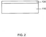
- FIG. 2is a schematic diagram illustrating a process of the method for forming a thin film photovoltaic device according to an embodiment of the present invention.
- the diagramis merely an example, which should not unduly limit the claims herein.
- a process for forming a thin film photovoltaic deviceis to form an electrode layer.
- an electrode layer 120is formed overlying the surface region 112 of the substrate 110 .
- the electrode layer 120can be made of molybdenum using sputtering, evaporation (e.g., electron beam), electro plating, combination of these, and the like according to a specific embodiment.
- the thickness of the electrode layercan be ranged from 100 nm to 2 micron and others, characterized by resistivity of about 100 Ohm/cm 2 to 10 Ohm/cm 2 and less according to a specific embodiment.
- the electrodeis made of molybdenum or tungsten, but can be others like copper, chromium, aluminum, nickel, or platinum. Of course, there can be other variations, modifications, and alternatives.
- FIG. 3is a schematic diagram illustrating a process of the method for forming a thin film photovoltaic device according to an embodiment of the present invention.
- the diagramis merely an example, which should not unduly limit the claims herein.
- a process of forming a copper layer overlying the electrode layer formed in last processis a process of forming a copper layer overlying the electrode layer formed in last process.
- a copper (Cu) layer 130is formed overlying the electrode layer 120 .
- the copper layeris formed using a sputtering process.
- a DC magnetron sputtering processcan be used to deposit Cu layer 130 onto the electrode layer 120 under a following condition.
- the deposition pressure(using Ar gas) is controlled to be about 6.2 mTorr.
- the gas flow rateis set to about 32 sccm.
- the deposition temperaturecan be just at room temperature without need of intentionally heating the substrate. Of course, minor heating may be resulted due to the plasma generated during the deposition. Additionally, the DC power supply of about 115 W may be required. According to certain embodiments, DC power in a range from 100 W to 150 W is suitable depending specific cases with different materials.
- the full deposition time for a Cu layer of 330 nm thicknessis about 6 minutes or more.
- the deposition conditioncan be varied and modified according to a specific embodiment.
- the sputtering process of Cucan be performed using a Cu—Ga alloy target. Therefore, the Cu layer 130 can contain at least partially a desirable and adjustable amount of Ga species within the final metal precursor film.
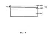
- FIG. 4is a schematic diagram illustrating a process of the method for forming a thin film photovoltaic device according to an embodiment of the present invention.
- the diagramis merely an example, which should not unduly limit the claims herein.
- One skilled in the artwould recognize other variations, modifications, and alternatives.
- a process of providing an indium (In) layer overlying the copper (Cu) layeris illustrated.
- the indium layer 140is formed overlying the copper layer 130 .
- the indium layeris deposited over the copper layer using a sputtering process.
- a DC magnetron sputtering processcan be used to deposit In layer 140 overlying the Cu layer 130 under a similar condition for depositing the Cu layer.
- the sputtering process to deposit In layer 140can be performed by using an In—Ga alloy target to form an In—Ga layer overlying the Cu layer 130 .
- the Ga contentcan be adjusted to a desired level by selecting a proper concentration ratio in the In—Ga alloy target and some deposition conditions. This Ga content at least partially contributes final Ga species and ratio of Cu/(In+Ga) within the metal precursor film for forming the absorber layer of the solar cell.
- the deposition time for the indium layermay be shorter than that for Cu layer. For example, 2 minutes and 45 seconds may be enough for depositing an In layer of about 410 nm in thickness.
- the indium layeris provided overlying the copper layer by an electro plating process, or others dependent on specific embodiment.
- FIGS. 1 through 4illustrate a formation of a multilayered structure 150 comprising copper and indium on a transparent substrate provided by processes of a method of forming a thin film photovoltaic device.
- the copper layer 130 as well as the indium layer 140are provided with an stoichiometric control to ensure that the formed multilayered structure 150 is a Cu-rich material with an atomic ratio of Cu:In greater than 1 therein.
- the atomic ratio of Cu:Incan be in a range from 1.2:1 to 2.0:1.
- the atomic ratio of Cu:Inis between 1.35:1 and 1.60:1.
- the atomic ratio of Cu:Inis selected to be about 1.55:1.
- the formation process of indium layer 140substantially causes no change in atomic stoichiometry in the copper layer 130 formed earlier. In another specific embodiment, the formation process of the indium layer 140 is performed earlier overlying the electrode layer 120 while the formation process of the copper layer 130 is performed later overlying the indium layer 140 .
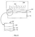
- FIG. 5is a schematic diagram illustrating a process of the method for forming a thin film photovoltaic device according to an embodiment of the present invention.
- the diagramis merely an example, which should not unduly limit the claims herein.
- the formed multilayered structure 150comprising at least an indium layer 140 over a copper layer 130 is subjected to a thermal treatment process 200 in an environment containing a sulfur bearing species 210 at an adequate pressure and at a temperature of about 400 Degrees Celsius to about 600 Degrees Celsius for about three to fifteen minutes for a rapid thermal process according to a specific embodiment.
- the sulfur bearing speciesare in a fluid phase.
- the sulfurcan be provided in a solution, which has dissolved Na 2 S, CS 2 , (NH 4 ) 2 S, thiosulfate, and others.
- the sulfur bearing species 210are hydrogen sulfide in gas phase.
- the sulfurcan be provided in a solid phase. In a solid phase, elemental sulfur can be heated and allowed to boil, which vaporizes into a gas phase, e.g., Sn. In a specific embodiment, the gas phase is allowed to react to the indium/copper layers. In other embodiments, other combinations of sulfur species can be used.
- the thermal treatment process 200includes certain predetermined ramp-up and ramp down period with certain predetermined speed for temperature changes.
- the thermal treatment processis a rapid thermal annealing process.
- the hydrogen sulfide gasis provided through one or more entry valves with flow rate control into the process chamber where the hydrogen sulfide gas pressure is under controlled by one or more pumps.
- entry valveswith flow rate control into the process chamber where the hydrogen sulfide gas pressure is under controlled by one or more pumps.
- the sulfurcan be provided as a layer overlying the indium and copper layers or copper and indium layers.
- the sulfur materialis provided as a thin layer or patterned layer.
- the sulfurcan be provided as a slurry, powder, solid material, gas, paste, or other suitable form.
- the thermal treatment process 200causes a reaction between copper indium material within the multilayered structure 150 and the sulfur bearing species 210 , thereby forming a layer of copper indium disulfide material (or a copper indium disulfide thin film) 220 .
- the copper indium disulfide material or copper indium disulfide thin film 220is transformed by incorporating sulfur ions/atoms stripped or decomposed from the sulfur bearing species into the multilayered structure 150 with indium atoms and copper atoms mutually diffused therein.
- the thermal treatment process 200would result in a formation of a cap layer over the transformed copper indium disulfide material 220 .
- the cap layercontains a thickness of substantially copper sulfide material 221 but substantially free of indium atoms.
- the copper sulfide material 221includes a surface region 225 of the same copper sulfide material substantially free of indium atoms.
- the formation of this cap layeris under a Cu-rich conditions for the original Cu—In bearing multilayered structure 150 .
- the thickness of the copper sulfide material 221is on an order of about five to ten nanometers and greater based on original multilayered structure 150 with indium layer 140 overlying copper layer 130 .
- FIG. 6is a schematic diagram illustrating a process of the method for forming a thin film photovoltaic device according to an embodiment of the present invention.
- the diagramis merely an example, which should not unduly limit the claims herein.
- a dip process 300is performed to the copper sulfide material 221 that covers the copper indium disulfide thin film 220 .
- the dip processis performed by exposing the surface region 225 to 1 about 10 weight % solution of potassium cyanide 310 according to a specific embodiment.
- the potassium cyanideacts as an etchant that is capable of selectively removing copper sulfide material 221 .
- the etching processstarts from the exposed surface region 225 and down to the thickness of the copper sulfide material 221 and substantially stopped at the interface between the copper sulfide material 221 and copper indium disulfide material 220 .
- the copper sulfide cap layer 221is selectively removed by the etching process so that a new surface region 228 of the remaining copper indium disulfide thin film 220 is exposed according to a specific embodiment.
- the etch selectivityis about 1:100 or more between copper sulfide and copper indium disulfide.
- other selective etching speciescan be used.
- the etching speciescan be hydrogen peroxide.
- the copper sulfide materialcan be mechanically removed, chemically removed, electrically removed, or any combination of these, among others.
- the absorber layer made of copper indium disulfideis about 1 to 10 microns, but can be others. Of course, there can be other variations, modifications, and alternatives.
- FIG. 7is a schematic diagram illustrating a process of the method for forming a thin film photovoltaic device according to an embodiment of the present invention.
- the diagramis merely an example, which should not unduly limit the claims herein.
- One skilled in the artwould recognize other variations, modifications, and alternatives.
- a p-type copper indium disulfide film 320is formed.
- the previously-formed copper indium disulfide material 220has possessed a p-type semiconducting characteristic and is substantially the same as the p-type copper indium disulfide film 320 .
- the copper indium disulfide material 220is subjected to additional doping process to adjust p-type impurity density therein for the purpose of optimizing I-V characteristic of the high efficiency thin film photovoltaic devices.
- aluminum speciesare mixed into the copper indium disulfide material 220 .
- the copper indium disulfide material 220is mixed with a copper indium aluminum disulfide material to form the film 320 .
- a window layer 310is formed overlying the p-type copper indium disulfide material 320 .
- the window layer 310can be selected from a group materials consisting of a cadmium sulfide (CdS), a zinc sulfide (ZnS), zinc selinium (ZnSe), zinc oxide (ZnO), zinc magnesium oxide (ZnMgO), or others and may be doped with impurities for conductivity, e.g., n + type.
- the window layer 310is intended to serve another part of a PN-junction associated with a photovoltaic cell.
- the window layer 310is heavily doped to form a n + -type semiconductor layer.
- indium speciesare used as the doping material to cause formation of the n + -type characteristic associated with the window layer 310 .
- the doping processis performed using suitable conditions.
- ZnO window layer that is doped with aluminumcan range from about 200 to 500 nanometers.
- FIG. 8is a schematic diagram illustrating a process of the method for forming a thin film photovoltaic device according to an embodiment of the present invention.
- the diagramis merely an example, which should not unduly limit the claims herein.
- a conductive layer 330is added at least partially on top of the window layer 310 to form a top electrode layer for the photovoltaic device.
- the conductive layer 330is a transparent conductive oxide TCO layer.
- TCOcan be selected from a group consisting of In 2 O 3 :Sn (ITO), ZnO:Al (AZO), SnO 2 :F (TFO), and can be others.
- the formation of the TCO layeris followed a certain predetermined pattern for effectively carried out the function of top electrode layer for the photovoltaic device with considerations of maximizing the efficiency of the thin film based photovoltaic devices.
- the TCOcan also act as a window layer, which essentially eliminates a separate window layer.
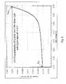
- FIG. 9is an exemplary solar cell I-V characteristics plot measured from a copper indium disulfide based thin film photovoltaic cell according to an embodiment of the present invention.
- the diagramis merely an example, which should not unduly limit the claims herein.
- One skilled in the artwould recognize other variations, modifications, and alternatives.
- a current density of a high efficiency copper indium disulfide thin film photovoltaic cell made according to an embodiment of the present inventionis plotted against a bias voltage.
- the curveintersects the y-axis with a short circuit current value at about 0.0235 A/cm 2 and intersects a zero current line with a bias at about 0.69 V.
- the corresponding photovoltaic cellhas an absorber layer made from copper indium disulfide thin film according to an embodiment of the present invention.
- the absorber layeris about 1.5 ⁇ m in thickness and an atomic ratio of Cu:In at about 1.5:1. Based on standard formula, a cell conversion efficiency ⁇ can be estimated:
- J SCis the short circuit current density of the cell
- V OCis the open circuit bias voltage applied
- FFis the so-called fill factor defined as the ratio of the maximum power point divided by the open circuit voltage (Voc) and the short circuit current (J SC ).
- the input light irradiance (P in , in W/m 2 )under standard test conditions [i.e., STC that specifies a temperature of 25° C. and an irradiance of 1000 W/m2 with an air mass 1.5 (AM1.5) spectrum.] and the surface area of the solar cell (in m 2 ).
- STCthat specifies a temperature of 25° C. and an irradiance of 1000 W/m2 with an air mass 1.5 (AM1.5) spectrum.
- AM1.5air mass 1.5
- the bandgapis about 1.45 eV to 1.5 eV.
Landscapes
- Photovoltaic Devices (AREA)
Abstract
Description
- This application claims priority to U.S. Provisional Patent Application No. 61/059,253, filed Jun. 5, 2008, entitled “HIGH EFFICIENCY PHOTOVOLTAIC CELL AND MANUFACTURING METHOD” by inventor Howard W. H. Lee, commonly assigned and incorporated by reference herein for all purposes.
- Not Applicable
- Not Applicable
- The present invention relates generally to photovoltaic materials and manufacturing method. More particularly, the present invention provides a method and structure for manufacture of high efficiency thin film photovoltaic cells. Merely by way of example, the present method and materials include absorber materials made of copper indium disulfide species, copper tin sulfide, iron disulfide, or others for single junction cells or multi-junction cells.
- From the beginning of time, mankind has been challenged to find way of harnessing energy. Energy comes in the forms such as petrochemical, hydroelectric, nuclear, wind, biomass, solar, and more primitive forms such as wood and coal. Over the past century, modern civilization has relied upon petrochemical energy as an important energy source. Petrochemical energy includes gas and oil. Gas includes lighter forms such as butane and propane, commonly used to heat homes and serve as fuel for cooking. Gas also includes gasoline, diesel, and jet fuel, commonly used for transportation purposes. Heavier forms of petrochemicals can also be used to heat homes in some places. Unfortunately, the supply of petrochemical fuel is limited and essentially fixed based upon the amount available on the planet Earth. Additionally, as more people use petroleum products in growing amounts, it is rapidly becoming a scarce resource, which will eventually become depleted over time.
- More recently, environmentally clean and renewable sources of energy have been desired. An example of a clean source of energy is hydroelectric power. Hydroelectric power is derived from electric generators driven by the flow of water produced by dams such as the Hoover Dam in Nevada. The electric power generated is used to power a large portion of the city of Los Angeles in California. Clean and renewable sources of energy also include wind, waves, biomass, and the like. That is, windmills convert wind energy into more useful forms of energy such as electricity. Still other types of clean energy include solar energy. Specific details of solar energy can be found throughout the present background and more particularly below.
- Solar energy technology generally converts electromagnetic radiation from the sun to other useful forms of energy. These other forms of energy include thermal energy and electrical power. For electrical power applications, solar cells are often used. Although solar energy is environmentally clean and has been successful to a point, many limitations remain to be resolved before it becomes widely used throughout the world. As an example, one type of solar cell uses crystalline materials, which are derived from semiconductor material ingots. These crystalline materials can be used to fabricate optoelectronic devices that include photovoltaic and photodiode devices that convert electromagnetic radiation into electrical power. However, crystalline materials are often costly and difficult to make on a large scale. Additionally, devices made from such crystalline materials often have low energy conversion efficiencies. Other types of solar cells use “thin film” technology to form a thin film of photosensitive material to be used to convert electromagnetic radiation into electrical power. Similar limitations exist with the use of thin film technology in making solar cells. That is, efficiencies are often poor. Additionally, film reliability is often poor and cannot be used for extensive periods of time in conventional environmental applications. Often, thin films are difficult to mechanically integrate with each other. These and other limitations of these conventional technologies can be found throughout the present specification and more particularly below.
- From the above, it is seen that improved techniques for manufacturing photovoltaic materials and resulting devices are desired.
- According to embodiments of the present invention, a method and a structure for forming thin film semiconductor materials for photovoltaic applications are provided. More particularly, the present invention provides a method and structure for forming semiconductor materials used for the manufacture of high efficiency photovoltaic cells. Merely by way of example, the present method and materials include absorber materials made of copper indium disulfide species, copper tin sulfide, iron disulfide, or others for single junction cells or multi-junction cells.
- In a specific embodiment, a method for forming a thin film photovoltaic device includes providing a transparent substrate comprising a surface region. The method also includes forming a first electrode layer overlying the surface region and forming a copper layer overlying the first electrode layer. Additionally, the method includes forming an indium layer overlying the copper layer to form a multi-layered structure and subjecting at least the multi-layered structure to thermal treatment process in an environment containing a sulfur bearing species. The method further includes forming a copper indium disulfide material from at least the treatment process of the multi-layered structure. The copper indium disulfide material includes an atomic ratio of copper:indium (Cu:In) ranging from about 1.35:1 to about 1.60:1. Furthermore, the method includes forming a window layer overlying the copper indium disulfide material.
- In another specific embodiment, a method for forming a thin film photovoltaic device includes providing a transparent substrate comprising a surface region and forming a first electrode layer overlying the surface region. Additionally, the method includes forming a copper indium material comprising an atomic ratio of Cu:In ranging from about 1.35:1 to about 1.60:1 by at least sputtering a target comprising an indium copper material. The method further includes subjecting the copper indium material to thermal treatment process in an environment containing a sulfur bearing species. Furthermore, the method includes forming a copper indium disulfide material from at least the thermal treatment process of the copper indium material. Moreover, the method includes forming a window layer overlying the copper indium disulfide material.
- In a specific embodiment, the present invention provides a method for forming a thin film photovoltaic device. The method includes providing a transparent substrate comprising a surface region. The method forms a first electrode layer overlying the surface region of the transparent substrate and subjects one or more target materials including at least a copper material and an indium material with a plurality of particles comprising one or more inert species and an hydrogen disulfide species to release a plurality of copper species and indium species according to a preferred embodiment. The method includes forming a copper indium disulfide layer of material overlying the first electrode layer. In one embodiment, the copper indium disulfide material comprises an atomic ratio of copper:indium (Cu:In) ranging from about 1.35:1 to about 1.60:1. In another embodiment, the copper indium disulfide material comprises an atomic ratio of Cu:In ranging from about 1.2:1 to about 2:1. In a preferred embodiment, the method includes forming a window layer overlying the copper indium disulfide material.
- In another specific embodiment, a method for forming a thin film photovoltaic device includes providing a substrate comprising a surface region. The method also includes forming a first electrode layer overlying the surface region and forming a copper layer overlying the first electrode layer. Additionally, the method includes forming an indium layer overlying the copper layer to form a multi-layered structure and subjecting at least the multi-layered structure to thermal treatment process in an environment containing a sulfur bearing species. The method further includes forming a copper indium disulfide material from at least the treatment process of the multi-layered structure. The copper indium disulfide material is characterized by a thickness ranging from about 1 micron to about 2 microns and an atomic ratio of copper:indium (Cu:In) from about 1.4:1 to about 1.6:1. Furthermore, the method includes forming a window layer overlying the copper indium disulfide material. The copper indium disulfide material forms an absorber layer of a photovoltaic device characterized by an efficiency of about 10% and greater under a standard test condition.
- In yet another specific embodiment, the present invention provides a thin film photovoltaic device. The device includes a substrate comprising a surface region and a first electrode layer overlying the surface region. Additionally, the device includes an absorber layer including a copper indium disulfide material characterized by a thickness ranging from 1 micron to 2 microns and a copper-to-indium atomic ratio ranging from about 1.4:1 to about 1.6:1. Moreover, the device includes a window layer overlying the absorber layer and a characteristics of an energy conversion efficiency of about 10% and greater.
- Still further, the present invention provides a thin film photovoltaic device, which can be configured in a bifacial manner. The bifacial device can be configured to a tandem cell, or other multi-cell configuration. In a specific embodiment, the present device has a transparent substrate comprising a surface region and a first electrode layer overlying the surface region. The device also has a copper indium disulfide material on the first electrode layer. In a preferred embodiment, the copper indium disulfide material is characterized by a copper-to-indium atomic ratio ranging from about 1.35:1 to about 1.60:1. The device also has a window layer overlying the copper indium disulfide material. In a preferred embodiment, the device also has an efficiency of about 10% and greater and also has a bandgap ranging from about 1.4 eV to 1.5 eV, and preferably 1.45 eV to about 1.5 eV.
- Many benefits are achieved by ways of present invention. For example, the present invention uses starting materials that are commercially available to form a thin film of semiconductor bearing material overlying a suitable substrate member. The thin film of semiconductor bearing material can be further processed to form a semiconductor thin film material of desired characteristics, such as atomic stoichiometry, impurity concentration, carrier concentration, doping, and others. Additionally, the present method uses environmentally friendly materials that are relatively less toxic than other thin-film photovoltaic materials. In a specific embodiment, the present device including the absorber (CuInS2) is characterized by a bandgap at between about 1.45 eV to 1.5 eV, but can be others. In a specific embodiment, the bandgap can be higher for a CuInS2 absorber including a gallium species, which has been alloyed. In a preferred embodiment, the present method and device is bifacial and can be configured for a tandem or other multilevel cell arrangement. The bifacial cell would act as an upper or top cell according to a specific embodiment. Depending on the embodiment, one or more of the benefits can be achieved. These and other benefits will be described in more detailed throughout the present specification and particularly below.
- Merely by way of example, the present method and materials include absorber materials made of copper indium disulfide species, copper tin sulfide, iron disulfide, or others for single junction cells or multi-junction cells.
FIGS. 1-7 are schematic diagrams illustrating a method and structure for forming a thin film photovoltaic device according to an embodiment of the present invention; andFIG. 8 is a simplified flow chart summarizing a method for forming a thin film photovoltaic device according to an embodiment of the present invention.FIG. 9 is an exemplary solar cell I-V characteristics plot measured from a copper indium disulfide based thin film photovoltaic cell according to an embodiment of the present invention.- According to embodiments of the present invention, a method and a structure for forming semiconductor materials for photovoltaic applications are provided. More particularly, the present invention provides a method for manufacturing thin film photovoltaic devices. Merely by way of example, the method has been used to provide a copper indium disulfide thin film material for high efficiency solar cell application. But it would be recognized that the present invention has a much broader range of applicability, for example, embodiments of the present invention may be used to form other semiconducting thin films or multilayers comprising iron sulfide, cadmium sulfide, zinc selenide, and others, and metal oxides such as zinc oxide, iron oxide, copper oxide, and others.
FIG. 1 is a schematic diagram illustrating a process of a method for forming a thin film photovoltaic device according to an embodiment of the present invention. The diagram is merely an example, which should not unduly limit the claims herein. One skilled in the art would recognize other variations, modifications, and alternatives. As shown inFIG. 1 , asubstrate 110 is provided. In one embodiment, thesubstrate 110 includes a surface region112 and is held in a process stage within a process chamber (not shown). In another embodiment, thesubstrate 110 is an optically transparent solid material. For example, thesubstrate 110 can be a glass, quartz, fused silica. Or the substrate can be other materials, transparent or non-transparent, including a plastic, or metal, or foil, or semiconductor, or other composite materials. Of course there can be other variations, modifications, and alternatives.FIG. 2 is a schematic diagram illustrating a process of the method for forming a thin film photovoltaic device according to an embodiment of the present invention. The diagram is merely an example, which should not unduly limit the claims herein. One skilled in the art would recognize other variations, modifications, and alternatives. As shown inFIG. 2 , a process for forming a thin film photovoltaic device is to form an electrode layer. In particular, anelectrode layer 120 is formed overlying the surface region112 of thesubstrate 110. For example, theelectrode layer 120 can be made of molybdenum using sputtering, evaporation (e.g., electron beam), electro plating, combination of these, and the like according to a specific embodiment. The thickness of the electrode layer can be ranged from 100 nm to 2 micron and others, characterized by resistivity of about 100 Ohm/cm2to 10 Ohm/cm2and less according to a specific embodiment. In a preferred embodiment, the electrode is made of molybdenum or tungsten, but can be others like copper, chromium, aluminum, nickel, or platinum. Of course, there can be other variations, modifications, and alternatives.FIG. 3 is a schematic diagram illustrating a process of the method for forming a thin film photovoltaic device according to an embodiment of the present invention. The diagram is merely an example, which should not unduly limit the claims herein. One skilled in the art would recognize other variations, modifications, and alternatives. As shown is a process of forming a copper layer overlying the electrode layer formed in last process. In particular, a copper (Cu)layer 130 is formed overlying theelectrode layer 120. For example, the copper layer is formed using a sputtering process. In one example, a DC magnetron sputtering process can be used to depositCu layer 130 onto theelectrode layer 120 under a following condition. The deposition pressure (using Ar gas) is controlled to be about 6.2 mTorr. The gas flow rate is set to about 32 sccm. The deposition temperature can be just at room temperature without need of intentionally heating the substrate. Of course, minor heating may be resulted due to the plasma generated during the deposition. Additionally, the DC power supply of about 115 W may be required. According to certain embodiments, DC power in a range from 100 W to 150 W is suitable depending specific cases with different materials. The full deposition time for a Cu layer of 330 nm thickness is about 6 minutes or more. Of course, the deposition condition can be varied and modified according to a specific embodiment. For example, the sputtering process of Cu can be performed using a Cu—Ga alloy target. Therefore, theCu layer 130 can contain at least partially a desirable and adjustable amount of Ga species within the final metal precursor film.FIG. 4 is a schematic diagram illustrating a process of the method for forming a thin film photovoltaic device according to an embodiment of the present invention. The diagram is merely an example, which should not unduly limit the claims herein. One skilled in the art would recognize other variations, modifications, and alternatives. As shown, a process of providing an indium (In) layer overlying the copper (Cu) layer is illustrated. In particular, theindium layer 140 is formed overlying thecopper layer 130. For example, the indium layer is deposited over the copper layer using a sputtering process. In one example, a DC magnetron sputtering process can be used to deposit Inlayer 140 overlying theCu layer 130 under a similar condition for depositing the Cu layer. In another example, the sputtering process to deposit Inlayer 140 can be performed by using an In—Ga alloy target to form an In—Ga layer overlying theCu layer 130. The Ga content can be adjusted to a desired level by selecting a proper concentration ratio in the In—Ga alloy target and some deposition conditions. This Ga content at least partially contributes final Ga species and ratio of Cu/(In+Ga) within the metal precursor film for forming the absorber layer of the solar cell. The deposition time for the indium layer may be shorter than that for Cu layer. For example, 2 minutes and 45 seconds may be enough for depositing an In layer of about 410 nm in thickness. In another example, the indium layer is provided overlying the copper layer by an electro plating process, or others dependent on specific embodiment.- According to embodiments of the present invention,
FIGS. 1 through 4 illustrate a formation of amultilayered structure 150 comprising copper and indium on a transparent substrate provided by processes of a method of forming a thin film photovoltaic device. In one embodiment, thecopper layer 130 as well as theindium layer 140 are provided with an stoichiometric control to ensure that the formedmultilayered structure 150 is a Cu-rich material with an atomic ratio of Cu:In greater than1 therein. For example, the atomic ratio of Cu:In can be in a range from 1.2:1 to 2.0:1. In one implementation, the atomic ratio of Cu:In is between 1.35:1 and 1.60:1. In another implementation, the atomic ratio of Cu:In is selected to be about 1.55:1. In a specific embodiment, the formation process ofindium layer 140 substantially causes no change in atomic stoichiometry in thecopper layer 130 formed earlier. In another specific embodiment, the formation process of theindium layer 140 is performed earlier overlying theelectrode layer 120 while the formation process of thecopper layer 130 is performed later overlying theindium layer 140. FIG. 5 is a schematic diagram illustrating a process of the method for forming a thin film photovoltaic device according to an embodiment of the present invention. The diagram is merely an example, which should not unduly limit the claims herein. One skilled in the art would recognize other variations, modifications, and alternatives. As shown, the formedmultilayered structure 150 comprising at least anindium layer 140 over acopper layer 130 is subjected to athermal treatment process 200 in an environment containing asulfur bearing species 210 at an adequate pressure and at a temperature of about 400 Degrees Celsius to about 600 Degrees Celsius for about three to fifteen minutes for a rapid thermal process according to a specific embodiment. In one example, the sulfur bearing species are in a fluid phase. As an example, the sulfur can be provided in a solution, which has dissolved Na2S, CS2, (NH4)2S, thiosulfate, and others. In another example, thesulfur bearing species 210 are hydrogen sulfide in gas phase. In other embodiments, the sulfur can be provided in a solid phase. In a solid phase, elemental sulfur can be heated and allowed to boil, which vaporizes into a gas phase, e.g., Sn. In a specific embodiment, the gas phase is allowed to react to the indium/copper layers. In other embodiments, other combinations of sulfur species can be used. Of course, thethermal treatment process 200 includes certain predetermined ramp-up and ramp down period with certain predetermined speed for temperature changes. For example, the thermal treatment process is a rapid thermal annealing process. The hydrogen sulfide gas is provided through one or more entry valves with flow rate control into the process chamber where the hydrogen sulfide gas pressure is under controlled by one or more pumps. Of course, there can be other variations, modifications, and alternatives.- In a specific embodiment, the sulfur can be provided as a layer overlying the indium and copper layers or copper and indium layers. In a specific embodiment, the sulfur material is provided as a thin layer or patterned layer. Depending upon the embodiment, the sulfur can be provided as a slurry, powder, solid material, gas, paste, or other suitable form. Of course, there can be other variations, modifications, and alternatives.
- Referring to the
FIG. 5 , thethermal treatment process 200 causes a reaction between copper indium material within themultilayered structure 150 and thesulfur bearing species 210, thereby forming a layer of copper indium disulfide material (or a copper indium disulfide thin film)220. In one example, the copper indium disulfide material or copper indium disulfidethin film 220 is transformed by incorporating sulfur ions/atoms stripped or decomposed from the sulfur bearing species into themultilayered structure 150 with indium atoms and copper atoms mutually diffused therein. In one embodiment, thethermal treatment process 200 would result in a formation of a cap layer over the transformed copperindium disulfide material 220. The cap layer contains a thickness of substantiallycopper sulfide material 221 but substantially free of indium atoms. Thecopper sulfide material 221 includes asurface region 225 of the same copper sulfide material substantially free of indium atoms. In a specific embodiment, the formation of this cap layer is under a Cu-rich conditions for the original Cu—In bearingmultilayered structure 150. Depending on the applications, the thickness of thecopper sulfide material 221 is on an order of about five to ten nanometers and greater based on originalmultilayered structure 150 withindium layer 140overlying copper layer 130. Of course, there can be other variations, modifications, and alternatives. FIG. 6 is a schematic diagram illustrating a process of the method for forming a thin film photovoltaic device according to an embodiment of the present invention. The diagram is merely an example, which should not unduly limit the claims herein. One skilled in the art would recognize other variations, modifications, and alternatives. As shown inFIG. 6 , adip process 300 is performed to thecopper sulfide material 221 that covers the copper indium disulfidethin film 220. In particular, the dip process is performed by exposing thesurface region 225 to 1 about 10 weight % solution ofpotassium cyanide 310 according to a specific embodiment. The potassium cyanide acts as an etchant that is capable of selectively removingcopper sulfide material 221. The etching process starts from the exposedsurface region 225 and down to the thickness of thecopper sulfide material 221 and substantially stopped at the interface between thecopper sulfide material 221 and copperindium disulfide material 220. As a result the coppersulfide cap layer 221 is selectively removed by the etching process so that anew surface region 228 of the remaining copper indium disulfidethin film 220 is exposed according to a specific embodiment. In a preferred embodiment, the etch selectivity is about 1:100 or more between copper sulfide and copper indium disulfide. In other embodiments, other selective etching species can be used. In a specific embodiment, the etching species can be hydrogen peroxide. In other embodiments, other techniques including electro-chemical etching, plasma etching, sputter-etching, or any combination of these can be used. In a specific embodiment, the copper sulfide material can be mechanically removed, chemically removed, electrically removed, or any combination of these, among others. In a specific embodiment, the absorber layer made of copper indium disulfide is about 1 to 10 microns, but can be others. Of course, there can be other variations, modifications, and alternatives.FIG. 7 is a schematic diagram illustrating a process of the method for forming a thin film photovoltaic device according to an embodiment of the present invention. The diagram is merely an example, which should not unduly limit the claims herein. One skilled in the art would recognize other variations, modifications, and alternatives. As shown inFIG. 7 , a p-type copperindium disulfide film 320 is formed. In certain embodiments, the previously-formed copperindium disulfide material 220 has possessed a p-type semiconducting characteristic and is substantially the same as the p-type copperindium disulfide film 320. In another embodiment, the copperindium disulfide material 220 is subjected to additional doping process to adjust p-type impurity density therein for the purpose of optimizing I-V characteristic of the high efficiency thin film photovoltaic devices. In one example, aluminum species are mixed into the copperindium disulfide material 220. In another example, the copperindium disulfide material 220 is mixed with a copper indium aluminum disulfide material to form thefilm 320. Of course, there can be other variations, modifications, and alternatives.- Subsequently, a
window layer 310 is formed overlying the p-type copperindium disulfide material 320. Thewindow layer 310 can be selected from a group materials consisting of a cadmium sulfide (CdS), a zinc sulfide (ZnS), zinc selinium (ZnSe), zinc oxide (ZnO), zinc magnesium oxide (ZnMgO), or others and may be doped with impurities for conductivity, e.g., n+ type. Thewindow layer 310 is intended to serve another part of a PN-junction associated with a photovoltaic cell. Therefore, thewindow layer 310, during or after its formation, is heavily doped to form a n+-type semiconductor layer. In one example, indium species are used as the doping material to cause formation of the n+-type characteristic associated with thewindow layer 310. In another example, the doping process is performed using suitable conditions. In a specific embodiment, ZnO window layer that is doped with aluminum can range from about 200 to 500 nanometers. Of course, there can be other variations, modifications, and alternative FIG. 8 is a schematic diagram illustrating a process of the method for forming a thin film photovoltaic device according to an embodiment of the present invention. The diagram is merely an example, which should not unduly limit the claims herein. One skilled in the art would recognize other variations, modifications, and alternatives. As shown inFIG. 8 , aconductive layer 330 is added at least partially on top of thewindow layer 310 to form a top electrode layer for the photovoltaic device. In one embodiment, theconductive layer 330 is a transparent conductive oxide TCO layer. For example, TCO can be selected from a group consisting of In2O3:Sn (ITO), ZnO:Al (AZO), SnO2:F (TFO), and can be others. In another embodiment, the formation of the TCO layer is followed a certain predetermined pattern for effectively carried out the function of top electrode layer for the photovoltaic device with considerations of maximizing the efficiency of the thin film based photovoltaic devices. In a specific embodiment, the TCO can also act as a window layer, which essentially eliminates a separate window layer. Of course there can be other variations, modifications, and alternatives.FIG. 9 is an exemplary solar cell I-V characteristics plot measured from a copper indium disulfide based thin film photovoltaic cell according to an embodiment of the present invention. The diagram is merely an example, which should not unduly limit the claims herein. One skilled in the art would recognize other variations, modifications, and alternatives. As shown inFIG. 9 , a current density of a high efficiency copper indium disulfide thin film photovoltaic cell made according to an embodiment of the present invention is plotted against a bias voltage. The curve intersects the y-axis with a short circuit current value at about 0.0235 A/cm2and intersects a zero current line with a bias at about 0.69 V. The corresponding photovoltaic cell has an absorber layer made from copper indium disulfide thin film according to an embodiment of the present invention. In particular, the absorber layer is about 1.5 μm in thickness and an atomic ratio of Cu:In at about 1.5:1. Based on standard formula, a cell conversion efficiency η can be estimated:- where JSCis the short circuit current density of the cell, VOCis the open circuit bias voltage applied, FF is the so-called fill factor defined as the ratio of the maximum power point divided by the open circuit voltage (Voc) and the short circuit current (JSC). The input light irradiance (Pin, in W/m2) under standard test conditions [i.e., STC that specifies a temperature of 25° C. and an irradiance of 1000 W/m2 with an air mass 1.5 (AM1.5) spectrum.] and the surface area of the solar cell (in m2). Thus, a 10.4% efficiency can be accurately estimated for this particular cell made from a method according to embodiments of the present invention. In a specific embodiment, the bandgap is about 1.45 eV to 1.5 eV. Of course, there can be other variations, modifications, and alternatives.
- Although the above has been illustrated according to specific embodiments, there can be other modifications, alternatives, and variations. It is understood that the examples and embodiments described herein are for illustrative purposes only and that various modifications or changes in light thereof will be suggested to persons skilled in the art and are to be included within the spirit and purview of this application and scope of the appended claims.
Claims (44)
Priority Applications (4)
| Application Number | Priority Date | Filing Date | Title |
|---|---|---|---|
| US12/475,858US20090301562A1 (en) | 2008-06-05 | 2009-06-01 | High efficiency photovoltaic cell and manufacturing method |
| PCT/US2009/046161WO2009149204A1 (en) | 2008-06-05 | 2009-06-03 | High efficiency photovoltaic cell and manufacturing method |
| DE112009001336TDE112009001336T5 (en) | 2008-06-05 | 2009-06-03 | High efficiency photovoltaic cell and manufacturing process |
| CN2009801206507ACN102057492A (en) | 2008-06-05 | 2009-06-03 | High-efficiency photovoltaic cell and method of manufacture |
Applications Claiming Priority (2)
| Application Number | Priority Date | Filing Date | Title |
|---|---|---|---|
| US5925308P | 2008-06-05 | 2008-06-05 | |
| US12/475,858US20090301562A1 (en) | 2008-06-05 | 2009-06-01 | High efficiency photovoltaic cell and manufacturing method |
Publications (1)
| Publication Number | Publication Date |
|---|---|
| US20090301562A1true US20090301562A1 (en) | 2009-12-10 |
Family
ID=41398510
Family Applications (1)
| Application Number | Title | Priority Date | Filing Date |
|---|---|---|---|
| US12/475,858AbandonedUS20090301562A1 (en) | 2008-06-05 | 2009-06-01 | High efficiency photovoltaic cell and manufacturing method |
Country Status (4)
| Country | Link |
|---|---|
| US (1) | US20090301562A1 (en) |
| CN (1) | CN102057492A (en) |
| DE (1) | DE112009001336T5 (en) |
| WO (1) | WO2009149204A1 (en) |
Cited By (7)
| Publication number | Priority date | Publication date | Assignee | Title |
|---|---|---|---|---|
| US20100229921A1 (en)* | 2009-03-16 | 2010-09-16 | Stion Corporation | Tandem photovoltaic cell and method using three glass substrate configuration |
| US20110017298A1 (en)* | 2007-11-14 | 2011-01-27 | Stion Corporation | Multi-junction solar cell devices |
| US20110143487A1 (en)* | 2008-09-30 | 2011-06-16 | Stion Corporation | Method and Structure for Thin Film Tandem Photovoltaic Cell |
| US20110168245A1 (en)* | 2008-08-28 | 2011-07-14 | Stion Corporation | Four Terminal Multi-Junction Thin Film Photovoltaic Device and Method |
| US8232134B2 (en) | 2008-09-30 | 2012-07-31 | Stion Corporation | Rapid thermal method and device for thin film tandem cell |
| US8569613B1 (en) | 2008-09-29 | 2013-10-29 | Stion Corporation | Multi-terminal photovoltaic module including independent cells and related system |
| US20140109967A1 (en)* | 2012-10-24 | 2014-04-24 | Korea Institute Of Science And Technology | Thin film solar cells for windows based on low cost solution process and fabrication method thereof |
Families Citing this family (1)
| Publication number | Priority date | Publication date | Assignee | Title |
|---|---|---|---|---|
| CN108493285A (en)* | 2018-05-15 | 2018-09-04 | 华南理工大学 | A kind of cadmium telluride nano crystal solar cell and preparation method thereof based on environment-friendly type, the nanocrystalline buffer layer of nontoxic wide band gap semiconducter |
Citations (72)
| Publication number | Priority date | Publication date | Assignee | Title |
|---|---|---|---|---|
| US4239553A (en)* | 1979-05-29 | 1980-12-16 | University Of Delaware | Thin film photovoltaic cells having increased durability and operating life and method for making same |
| US4446916A (en)* | 1981-08-13 | 1984-05-08 | Hayes Claude Q C | Heat-absorbing heat sink |
| US4488948A (en)* | 1981-11-23 | 1984-12-18 | The Dow Chemical Company | Channel flow cathode assembly and electrolyzer |
| US4612411A (en)* | 1985-06-04 | 1986-09-16 | Atlantic Richfield Company | Thin film solar cell with ZnO window layer |
| US4658086A (en)* | 1985-06-03 | 1987-04-14 | Chevron Research Company | Photovoltaic cell package assembly for mechanically stacked photovoltaic cells |
| US4710589A (en)* | 1986-10-21 | 1987-12-01 | Ametek, Inc. | Heterojunction p-i-n photovoltaic cell |
| US4782377A (en)* | 1986-09-30 | 1988-11-01 | Colorado State University Research Foundation | Semiconducting metal silicide radiation detectors and source |
| US4996108A (en)* | 1989-01-17 | 1991-02-26 | Simon Fraser University | Sheets of transition metal dichalcogenides |
| US5125984A (en)* | 1990-05-31 | 1992-06-30 | Siemens Aktiengesellschaft | Induced junction chalcopyrite solar cell |
| US5261968A (en)* | 1992-01-13 | 1993-11-16 | Photon Energy, Inc. | Photovoltaic cell and method |
| US5261969A (en)* | 1992-04-14 | 1993-11-16 | The Boeing Company | Monolithic voltage-matched tandem photovoltaic cell and method for making same |
| US5397401A (en)* | 1992-06-29 | 1995-03-14 | Canon Kabushiki Kaisha | Semiconductor apparatus covered with a sealing resin composition |
| US5501744A (en)* | 1992-01-13 | 1996-03-26 | Photon Energy, Inc. | Photovoltaic cell having a p-type polycrystalline layer with large crystals |
| US5536333A (en)* | 1992-05-12 | 1996-07-16 | Solar Cells, Inc. | Process for making photovoltaic devices and resultant product |
| US5578503A (en)* | 1992-09-22 | 1996-11-26 | Siemens Aktiengesellschaft | Rapid process for producing a chalcopyrite semiconductor on a substrate |
| US5665175A (en)* | 1990-05-30 | 1997-09-09 | Safir; Yakov | Bifacial solar cell |
| US5733382A (en)* | 1995-12-18 | 1998-03-31 | Hanoka; Jack I. | Solar cell modules and method of making same |
| US6040521A (en)* | 1996-11-08 | 2000-03-21 | Showa Shell Sekiyu K.K. | N-type window layer for a thin film solar cell and method of making |
| US6066797A (en)* | 1997-03-27 | 2000-05-23 | Canon Kabushiki Kaisha | Solar cell module |
| US6257175B1 (en)* | 1997-09-15 | 2001-07-10 | Edward G. Mosher | Oxygen and hydrogen generator apparatus for internal combustion engines |
| US6288325B1 (en)* | 1998-07-14 | 2001-09-11 | Bp Corporation North America Inc. | Producing thin film photovoltaic modules with high integrity interconnects and dual layer contacts |
| US6310281B1 (en)* | 2000-03-16 | 2001-10-30 | Global Solar Energy, Inc. | Thin-film, flexible photovoltaic module |
| US6320115B1 (en)* | 1995-07-19 | 2001-11-20 | Canon Kabushiki Kaisha | Semicondonductor device and a process for the production thereof |
| US6328871B1 (en)* | 1999-08-16 | 2001-12-11 | Applied Materials, Inc. | Barrier layer for electroplating processes |
| US20010050234A1 (en)* | 1999-12-22 | 2001-12-13 | Shiepe Jason K. | Electrochemical cell system |
| US6350946B1 (en)* | 1999-09-10 | 2002-02-26 | Fuji Photo Film Co., Ltd. | Photoelectric conversion device and photoelectric cell |
| US20020026955A1 (en)* | 2000-07-21 | 2002-03-07 | Takashi Ouchida | Thin-film solar cell module |
| US20020038663A1 (en)* | 2000-07-06 | 2002-04-04 | Hideaki Zenko | Photovoltaic device assembly, solar cell module using the same and manufacture method of solar cell module |
| US6548751B2 (en)* | 2000-12-12 | 2003-04-15 | Solarflex Technologies, Inc. | Thin film flexible solar cell |
| US20030079772A1 (en)* | 2001-10-23 | 2003-05-01 | Gittings Bruce E. | Sealed photovoltaic modules |
| US20030227017A1 (en)* | 2002-06-07 | 2003-12-11 | Atsushi Yasuno | Photovoltaic device |
| US20050006228A1 (en)* | 2002-02-04 | 2005-01-13 | Jang-Soo Hyun | Brown's gas generator |
| US20050056312A1 (en)* | 2003-03-14 | 2005-03-17 | Young David L. | Bifacial structure for tandem solar cells |
| US20050109392A1 (en)* | 2002-09-30 | 2005-05-26 | Hollars Dennis R. | Manufacturing apparatus and method for large-scale production of thin-film solar cells |
| US20050150542A1 (en)* | 2004-01-13 | 2005-07-14 | Arun Madan | Stable Three-Terminal and Four-Terminal Solar Cells and Solar Cell Panels Using Thin-Film Silicon Technology |
| US20050183962A1 (en)* | 2004-02-24 | 2005-08-25 | Oakes Thomas W. | System and method for generating hydrogen gas using renewable energy |
| US20060037641A1 (en)* | 2002-08-16 | 2006-02-23 | Horst Kibbel | Body part of a vehicle provided with a thin-film solar cell and the production thereof |
| US20060130890A1 (en)* | 2004-12-20 | 2006-06-22 | Palo Alto Research Center Incorporated. | Heterojunction photovoltaic cell |
| US20060180197A1 (en)* | 2005-02-15 | 2006-08-17 | Gui John Y | Layer-to-layer interconnects for photoelectric devices and methods of fabricating the same |
| US20060180464A1 (en)* | 2003-08-19 | 2006-08-17 | Linnard Griffin | Apparatus and method for the controllable production of hydrogen at an accelerated rate |
| US20060220059A1 (en)* | 2003-04-09 | 2006-10-05 | Matsushita Electric Industrial Co., Ltd | Solar cell |
| US7141863B1 (en)* | 2002-11-27 | 2006-11-28 | University Of Toledo | Method of making diode structures |
| US20070089782A1 (en)* | 2003-10-02 | 2007-04-26 | Scheuten Glasgroep | Spherical or grain-shaped semiconductor element for use in solar cells and method for producing the same; method for producing a solar cell comprising said semiconductor element and solar cell |
| US20070093006A1 (en)* | 2005-10-24 | 2007-04-26 | Basol Bulent M | Technique For Preparing Precursor Films And Compound Layers For Thin Film Solar Cell Fabrication And Apparatus Corresponding Thereto |
| US20070151596A1 (en)* | 2004-02-20 | 2007-07-05 | Sharp Kabushiki Kaisha | Substrate for photoelectric conversion device, photoelectric conversion device, and stacked photoelectric conversion device |
| US20070160770A1 (en)* | 2006-01-12 | 2007-07-12 | Stanbery Billy J | Apparatus for making controlled segregated phase domain structures |
| US20070169810A1 (en)* | 2004-02-19 | 2007-07-26 | Nanosolar, Inc. | High-throughput printing of semiconductor precursor layer by use of chalcogen-containing vapor |
| US20080023059A1 (en)* | 2006-07-25 | 2008-01-31 | Basol Bulent M | Tandem solar cell structures and methods of manufacturing same |
| US20080041446A1 (en)* | 2006-08-09 | 2008-02-21 | Industrial Technology Research Institute | Dye-sensitized solar cells and method for fabricating same |
| US20080092953A1 (en)* | 2006-05-15 | 2008-04-24 | Stion Corporation | Method and structure for thin film photovoltaic materials using bulk semiconductor materials |
| US20080092945A1 (en)* | 2006-10-24 | 2008-04-24 | Applied Quantum Technology Llc | Semiconductor Grain and Oxide Layer for Photovoltaic Cells |
| US20080173390A1 (en)* | 2007-01-22 | 2008-07-24 | Mukundan Narasimhan | Finger pattern formation for thin film solar cells |
| US20080216885A1 (en)* | 2007-03-06 | 2008-09-11 | Sergey Frolov | Spectrally adaptive multijunction photovoltaic thin film device and method of producing same |
| US20080257751A1 (en)* | 2006-04-25 | 2008-10-23 | Smola Matthew M | Enhanced device for generating hydrogen for use in internal combustion engines |
| US20080257201A1 (en)* | 2007-04-18 | 2008-10-23 | James Harris | Fabrication of Electrically Active Films Based on Multiple Layers |
| US20090020149A1 (en)* | 2007-07-16 | 2009-01-22 | Woods Lawrence M | Hybrid Multi-Junction Photovoltaic Cells And Associated Methods |
| US20090194165A1 (en)* | 2008-01-31 | 2009-08-06 | Primestar Solar, Inc. | Ultra-high current density cadmium telluride photovoltaic modules |
| US20090308437A1 (en)* | 2006-09-19 | 2009-12-17 | Itn Energy Systems, Inc. | Systems And Processes For Bifacial Collection And Tandem Junctions Using A Thin-Film Photovoltaic Device |
| US20100051090A1 (en)* | 2008-08-28 | 2010-03-04 | Stion Corporation | Four terminal multi-junction thin film photovoltaic device and method |
| US20100078059A1 (en)* | 2008-09-30 | 2010-04-01 | Stion Corporation | Method and structure for thin film tandem photovoltaic cell |
| US20100099214A1 (en)* | 2008-06-25 | 2010-04-22 | Stion Corporation | Consumable adhesive layer for thin film photovoltaic material |
| US20100132775A1 (en)* | 2009-03-05 | 2010-06-03 | Applied Materials, Inc. | Adhesion between azo and ag for the back contact in tandem junction cell by metal alloy |
| US20100229921A1 (en)* | 2009-03-16 | 2010-09-16 | Stion Corporation | Tandem photovoltaic cell and method using three glass substrate configuration |
| US20100236610A1 (en)* | 2007-09-03 | 2010-09-23 | Robert Stancel | Mounting System for Solar Modules |
| US20100307552A1 (en)* | 2008-03-25 | 2010-12-09 | Corning Incorporated | Methods for coating a substrate |
| US7855089B2 (en)* | 2008-09-10 | 2010-12-21 | Stion Corporation | Application specific solar cell and method for manufacture using thin film photovoltaic materials |
| US7863074B2 (en)* | 2008-09-30 | 2011-01-04 | Stion Corporation | Patterning electrode materials free from berm structures for thin film photovoltaic cells |
| US20110017298A1 (en)* | 2007-11-14 | 2011-01-27 | Stion Corporation | Multi-junction solar cell devices |
| US20110017257A1 (en)* | 2008-08-27 | 2011-01-27 | Stion Corporation | Multi-junction solar module and method for current matching between a plurality of first photovoltaic devices and second photovoltaic devices |
| US7910399B1 (en)* | 2008-09-30 | 2011-03-22 | Stion Corporation | Thermal management and method for large scale processing of CIS and/or CIGS based thin films overlying glass substrates |
| US20120199065A1 (en)* | 2011-02-04 | 2012-08-09 | Stion Corporation | Multi-Module System for Processing Thin Film Photovoltaic Devices |
| US20120204939A1 (en)* | 2010-08-23 | 2012-08-16 | Stion Corporation | Structure and Method for High Efficiency CIS/CIGS-based Tandem Photovoltaic Module |
- 2009
- 2009-06-01USUS12/475,858patent/US20090301562A1/ennot_activeAbandoned
- 2009-06-03CNCN2009801206507Apatent/CN102057492A/enactivePending
- 2009-06-03WOPCT/US2009/046161patent/WO2009149204A1/enactiveApplication Filing
- 2009-06-03DEDE112009001336Tpatent/DE112009001336T5/ennot_activeWithdrawn
Patent Citations (73)
| Publication number | Priority date | Publication date | Assignee | Title |
|---|---|---|---|---|
| US4239553A (en)* | 1979-05-29 | 1980-12-16 | University Of Delaware | Thin film photovoltaic cells having increased durability and operating life and method for making same |
| US4446916A (en)* | 1981-08-13 | 1984-05-08 | Hayes Claude Q C | Heat-absorbing heat sink |
| US4488948A (en)* | 1981-11-23 | 1984-12-18 | The Dow Chemical Company | Channel flow cathode assembly and electrolyzer |
| US4658086A (en)* | 1985-06-03 | 1987-04-14 | Chevron Research Company | Photovoltaic cell package assembly for mechanically stacked photovoltaic cells |
| US4612411A (en)* | 1985-06-04 | 1986-09-16 | Atlantic Richfield Company | Thin film solar cell with ZnO window layer |
| US4782377A (en)* | 1986-09-30 | 1988-11-01 | Colorado State University Research Foundation | Semiconducting metal silicide radiation detectors and source |
| US4710589A (en)* | 1986-10-21 | 1987-12-01 | Ametek, Inc. | Heterojunction p-i-n photovoltaic cell |
| US4996108A (en)* | 1989-01-17 | 1991-02-26 | Simon Fraser University | Sheets of transition metal dichalcogenides |
| US5665175A (en)* | 1990-05-30 | 1997-09-09 | Safir; Yakov | Bifacial solar cell |
| US5125984A (en)* | 1990-05-31 | 1992-06-30 | Siemens Aktiengesellschaft | Induced junction chalcopyrite solar cell |
| US5501744A (en)* | 1992-01-13 | 1996-03-26 | Photon Energy, Inc. | Photovoltaic cell having a p-type polycrystalline layer with large crystals |
| US5261968A (en)* | 1992-01-13 | 1993-11-16 | Photon Energy, Inc. | Photovoltaic cell and method |
| US5261969A (en)* | 1992-04-14 | 1993-11-16 | The Boeing Company | Monolithic voltage-matched tandem photovoltaic cell and method for making same |
| US5536333A (en)* | 1992-05-12 | 1996-07-16 | Solar Cells, Inc. | Process for making photovoltaic devices and resultant product |
| US5397401A (en)* | 1992-06-29 | 1995-03-14 | Canon Kabushiki Kaisha | Semiconductor apparatus covered with a sealing resin composition |
| US5578503A (en)* | 1992-09-22 | 1996-11-26 | Siemens Aktiengesellschaft | Rapid process for producing a chalcopyrite semiconductor on a substrate |
| US6320115B1 (en)* | 1995-07-19 | 2001-11-20 | Canon Kabushiki Kaisha | Semicondonductor device and a process for the production thereof |
| US5733382A (en)* | 1995-12-18 | 1998-03-31 | Hanoka; Jack I. | Solar cell modules and method of making same |
| US6040521A (en)* | 1996-11-08 | 2000-03-21 | Showa Shell Sekiyu K.K. | N-type window layer for a thin film solar cell and method of making |
| US6066797A (en)* | 1997-03-27 | 2000-05-23 | Canon Kabushiki Kaisha | Solar cell module |
| US6257175B1 (en)* | 1997-09-15 | 2001-07-10 | Edward G. Mosher | Oxygen and hydrogen generator apparatus for internal combustion engines |
| US6288325B1 (en)* | 1998-07-14 | 2001-09-11 | Bp Corporation North America Inc. | Producing thin film photovoltaic modules with high integrity interconnects and dual layer contacts |
| US6328871B1 (en)* | 1999-08-16 | 2001-12-11 | Applied Materials, Inc. | Barrier layer for electroplating processes |
| US6350946B1 (en)* | 1999-09-10 | 2002-02-26 | Fuji Photo Film Co., Ltd. | Photoelectric conversion device and photoelectric cell |
| US20010050234A1 (en)* | 1999-12-22 | 2001-12-13 | Shiepe Jason K. | Electrochemical cell system |
| US6310281B1 (en)* | 2000-03-16 | 2001-10-30 | Global Solar Energy, Inc. | Thin-film, flexible photovoltaic module |
| US20020038663A1 (en)* | 2000-07-06 | 2002-04-04 | Hideaki Zenko | Photovoltaic device assembly, solar cell module using the same and manufacture method of solar cell module |
| US20020026955A1 (en)* | 2000-07-21 | 2002-03-07 | Takashi Ouchida | Thin-film solar cell module |
| US6548751B2 (en)* | 2000-12-12 | 2003-04-15 | Solarflex Technologies, Inc. | Thin film flexible solar cell |
| US20030079772A1 (en)* | 2001-10-23 | 2003-05-01 | Gittings Bruce E. | Sealed photovoltaic modules |
| US20050006228A1 (en)* | 2002-02-04 | 2005-01-13 | Jang-Soo Hyun | Brown's gas generator |
| US20030227017A1 (en)* | 2002-06-07 | 2003-12-11 | Atsushi Yasuno | Photovoltaic device |
| US20060037641A1 (en)* | 2002-08-16 | 2006-02-23 | Horst Kibbel | Body part of a vehicle provided with a thin-film solar cell and the production thereof |
| US6974976B2 (en)* | 2002-09-30 | 2005-12-13 | Miasole | Thin-film solar cells |
| US20050109392A1 (en)* | 2002-09-30 | 2005-05-26 | Hollars Dennis R. | Manufacturing apparatus and method for large-scale production of thin-film solar cells |
| US7141863B1 (en)* | 2002-11-27 | 2006-11-28 | University Of Toledo | Method of making diode structures |
| US20050056312A1 (en)* | 2003-03-14 | 2005-03-17 | Young David L. | Bifacial structure for tandem solar cells |
| US20060220059A1 (en)* | 2003-04-09 | 2006-10-05 | Matsushita Electric Industrial Co., Ltd | Solar cell |
| US20060180464A1 (en)* | 2003-08-19 | 2006-08-17 | Linnard Griffin | Apparatus and method for the controllable production of hydrogen at an accelerated rate |
| US20070089782A1 (en)* | 2003-10-02 | 2007-04-26 | Scheuten Glasgroep | Spherical or grain-shaped semiconductor element for use in solar cells and method for producing the same; method for producing a solar cell comprising said semiconductor element and solar cell |
| US20050150542A1 (en)* | 2004-01-13 | 2005-07-14 | Arun Madan | Stable Three-Terminal and Four-Terminal Solar Cells and Solar Cell Panels Using Thin-Film Silicon Technology |
| US20070169810A1 (en)* | 2004-02-19 | 2007-07-26 | Nanosolar, Inc. | High-throughput printing of semiconductor precursor layer by use of chalcogen-containing vapor |
| US20070151596A1 (en)* | 2004-02-20 | 2007-07-05 | Sharp Kabushiki Kaisha | Substrate for photoelectric conversion device, photoelectric conversion device, and stacked photoelectric conversion device |
| US20050183962A1 (en)* | 2004-02-24 | 2005-08-25 | Oakes Thomas W. | System and method for generating hydrogen gas using renewable energy |
| US20060130890A1 (en)* | 2004-12-20 | 2006-06-22 | Palo Alto Research Center Incorporated. | Heterojunction photovoltaic cell |
| US20060180197A1 (en)* | 2005-02-15 | 2006-08-17 | Gui John Y | Layer-to-layer interconnects for photoelectric devices and methods of fabricating the same |
| US20070093006A1 (en)* | 2005-10-24 | 2007-04-26 | Basol Bulent M | Technique For Preparing Precursor Films And Compound Layers For Thin Film Solar Cell Fabrication And Apparatus Corresponding Thereto |
| US20070160770A1 (en)* | 2006-01-12 | 2007-07-12 | Stanbery Billy J | Apparatus for making controlled segregated phase domain structures |
| US20080257751A1 (en)* | 2006-04-25 | 2008-10-23 | Smola Matthew M | Enhanced device for generating hydrogen for use in internal combustion engines |
| US20080092953A1 (en)* | 2006-05-15 | 2008-04-24 | Stion Corporation | Method and structure for thin film photovoltaic materials using bulk semiconductor materials |
| US20080023059A1 (en)* | 2006-07-25 | 2008-01-31 | Basol Bulent M | Tandem solar cell structures and methods of manufacturing same |
| US20080041446A1 (en)* | 2006-08-09 | 2008-02-21 | Industrial Technology Research Institute | Dye-sensitized solar cells and method for fabricating same |
| US20090308437A1 (en)* | 2006-09-19 | 2009-12-17 | Itn Energy Systems, Inc. | Systems And Processes For Bifacial Collection And Tandem Junctions Using A Thin-Film Photovoltaic Device |
| US20080092945A1 (en)* | 2006-10-24 | 2008-04-24 | Applied Quantum Technology Llc | Semiconductor Grain and Oxide Layer for Photovoltaic Cells |
| US20080173390A1 (en)* | 2007-01-22 | 2008-07-24 | Mukundan Narasimhan | Finger pattern formation for thin film solar cells |
| US20080216885A1 (en)* | 2007-03-06 | 2008-09-11 | Sergey Frolov | Spectrally adaptive multijunction photovoltaic thin film device and method of producing same |
| US20080257201A1 (en)* | 2007-04-18 | 2008-10-23 | James Harris | Fabrication of Electrically Active Films Based on Multiple Layers |
| US20090020149A1 (en)* | 2007-07-16 | 2009-01-22 | Woods Lawrence M | Hybrid Multi-Junction Photovoltaic Cells And Associated Methods |
| US20100236610A1 (en)* | 2007-09-03 | 2010-09-23 | Robert Stancel | Mounting System for Solar Modules |
| US20110017298A1 (en)* | 2007-11-14 | 2011-01-27 | Stion Corporation | Multi-junction solar cell devices |
| US20090194165A1 (en)* | 2008-01-31 | 2009-08-06 | Primestar Solar, Inc. | Ultra-high current density cadmium telluride photovoltaic modules |
| US20100307552A1 (en)* | 2008-03-25 | 2010-12-09 | Corning Incorporated | Methods for coating a substrate |
| US20100099214A1 (en)* | 2008-06-25 | 2010-04-22 | Stion Corporation | Consumable adhesive layer for thin film photovoltaic material |
| US20110017257A1 (en)* | 2008-08-27 | 2011-01-27 | Stion Corporation | Multi-junction solar module and method for current matching between a plurality of first photovoltaic devices and second photovoltaic devices |
| US20100051090A1 (en)* | 2008-08-28 | 2010-03-04 | Stion Corporation | Four terminal multi-junction thin film photovoltaic device and method |
| US7855089B2 (en)* | 2008-09-10 | 2010-12-21 | Stion Corporation | Application specific solar cell and method for manufacture using thin film photovoltaic materials |
| US7863074B2 (en)* | 2008-09-30 | 2011-01-04 | Stion Corporation | Patterning electrode materials free from berm structures for thin film photovoltaic cells |
| US20100078059A1 (en)* | 2008-09-30 | 2010-04-01 | Stion Corporation | Method and structure for thin film tandem photovoltaic cell |
| US7910399B1 (en)* | 2008-09-30 | 2011-03-22 | Stion Corporation | Thermal management and method for large scale processing of CIS and/or CIGS based thin films overlying glass substrates |
| US20100132775A1 (en)* | 2009-03-05 | 2010-06-03 | Applied Materials, Inc. | Adhesion between azo and ag for the back contact in tandem junction cell by metal alloy |
| US20100229921A1 (en)* | 2009-03-16 | 2010-09-16 | Stion Corporation | Tandem photovoltaic cell and method using three glass substrate configuration |
| US20120204939A1 (en)* | 2010-08-23 | 2012-08-16 | Stion Corporation | Structure and Method for High Efficiency CIS/CIGS-based Tandem Photovoltaic Module |
| US20120199065A1 (en)* | 2011-02-04 | 2012-08-09 | Stion Corporation | Multi-Module System for Processing Thin Film Photovoltaic Devices |
Cited By (10)
| Publication number | Priority date | Publication date | Assignee | Title |
|---|---|---|---|---|
| US20110017298A1 (en)* | 2007-11-14 | 2011-01-27 | Stion Corporation | Multi-junction solar cell devices |
| US8907206B2 (en) | 2007-11-14 | 2014-12-09 | Stion Corporation | Multi-junction solar cell devices |
| US20110168245A1 (en)* | 2008-08-28 | 2011-07-14 | Stion Corporation | Four Terminal Multi-Junction Thin Film Photovoltaic Device and Method |
| US8569613B1 (en) | 2008-09-29 | 2013-10-29 | Stion Corporation | Multi-terminal photovoltaic module including independent cells and related system |
| US20110143487A1 (en)* | 2008-09-30 | 2011-06-16 | Stion Corporation | Method and Structure for Thin Film Tandem Photovoltaic Cell |
| US8232134B2 (en) | 2008-09-30 | 2012-07-31 | Stion Corporation | Rapid thermal method and device for thin film tandem cell |
| US8889468B2 (en) | 2008-09-30 | 2014-11-18 | Stion Corporation | Method and structure for thin film tandem photovoltaic cell |
| US20100229921A1 (en)* | 2009-03-16 | 2010-09-16 | Stion Corporation | Tandem photovoltaic cell and method using three glass substrate configuration |
| US8563850B2 (en) | 2009-03-16 | 2013-10-22 | Stion Corporation | Tandem photovoltaic cell and method using three glass substrate configuration |
| US20140109967A1 (en)* | 2012-10-24 | 2014-04-24 | Korea Institute Of Science And Technology | Thin film solar cells for windows based on low cost solution process and fabrication method thereof |
Also Published As
| Publication number | Publication date |
|---|---|
| CN102057492A (en) | 2011-05-11 |
| DE112009001336T5 (en) | 2011-04-21 |
| WO2009149204A1 (en) | 2009-12-10 |
Similar Documents
| Publication | Publication Date | Title |
|---|---|---|
| US8344243B2 (en) | Method and structure for thin film photovoltaic cell using similar material junction | |
| US8198122B2 (en) | Bulk chloride species treatment of thin film photovoltaic cell and manufacturing method | |
| US8008110B1 (en) | Bulk sodium species treatment of thin film photovoltaic cell and manufacturing method | |
| US7960204B2 (en) | Method and structure for adhesion of absorber material for thin film photovoltaic cell | |
| US8003430B1 (en) | Sulfide species treatment of thin film photovoltaic cell and manufacturing method | |
| US8889468B2 (en) | Method and structure for thin film tandem photovoltaic cell | |
| US8008111B1 (en) | Bulk copper species treatment of thin film photovoltaic cell and manufacturing method | |
| US8617917B2 (en) | Consumable adhesive layer for thin film photovoltaic material | |
| US8026122B1 (en) | Metal species surface treatment of thin film photovoltaic cell and manufacturing method | |
| US8425739B1 (en) | In chamber sodium doping process and system for large scale cigs based thin film photovoltaic materials | |
| US20090301562A1 (en) | High efficiency photovoltaic cell and manufacturing method | |
| US8232134B2 (en) | Rapid thermal method and device for thin film tandem cell | |
| US9087943B2 (en) | High efficiency photovoltaic cell and manufacturing method free of metal disulfide barrier material | |
| US8394662B1 (en) | Chloride species surface treatment of thin film photovoltaic cell and manufacturing method | |
| US8435826B1 (en) | Bulk sulfide species treatment of thin film photovoltaic cell and manufacturing method | |
| US8236597B1 (en) | Bulk metal species treatment of thin film photovoltaic cell and manufacturing method | |
| US8476104B1 (en) | Sodium species surface treatment of thin film photovoltaic cell and manufacturing method | |
| US8501521B1 (en) | Copper species surface treatment of thin film photovoltaic cell and manufacturing method | |
| US8642138B2 (en) | Processing method for cleaning sulfur entities of contact regions | |
| US8082672B2 (en) | Mechanical patterning of thin film photovoltaic materials and structure |
Legal Events
| Date | Code | Title | Description |
|---|---|---|---|
| AS | Assignment | Owner name:STION CORPORATION, CALIFORNIA Free format text:ASSIGNMENT OF ASSIGNORS INTEREST;ASSIGNOR:LEE, HOWARD W.H.;REEL/FRAME:022884/0466 Effective date:20090617 | |
| AS | Assignment | Owner name:STION CORPORATION, CALIFORNIA Free format text:ASSIGNMENT OF ASSIGNORS INTEREST;ASSIGNOR:LEE, HOWARD W.H.;REEL/FRAME:022943/0126 Effective date:20090617 | |
| AS | Assignment | Owner name:CM MANUFACTURING, INC., CALIFORNIA Free format text:CHANGE OF NAME;ASSIGNOR:STION CORPORATION;REEL/FRAME:032144/0774 Effective date:20131011 | |
| AS | Assignment | Owner name:HETF SOLAR INC., CALIFORNIA Free format text:SECURITY AGREEMENT;ASSIGNOR:DEVELOPMENT SPECIALIST, INC., SOLELY IN ITS CAPACITY AS THE ASSIGNEE FOR THE BENEFIT OF THE CREDITORS OF CM MANUFACTURING, INC. (F/K/A STION CORPORATION), AND CM MANUFACTURING (F/K/A STION CORPORATION);REEL/FRAME:032209/0879 Effective date:20131022 | |
| AS | Assignment | Owner name:STION CORPORATION, CALIFORNIA Free format text:CHANGE OF NAME;ASSIGNOR:HETF SOLAR INC.;REEL/FRAME:032324/0402 Effective date:20131025 | |
| STCB | Information on status: application discontinuation | Free format text:ABANDONED -- FAILURE TO RESPOND TO AN OFFICE ACTION |