US20090298257A1 - Device isolation technology on semiconductor substrate - Google Patents
Device isolation technology on semiconductor substrateDownload PDFInfo
- Publication number
- US20090298257A1 US20090298257A1US12/130,522US13052208AUS2009298257A1US 20090298257 A1US20090298257 A1US 20090298257A1US 13052208 AUS13052208 AUS 13052208AUS 2009298257 A1US2009298257 A1US 2009298257A1
- Authority
- US
- United States
- Prior art keywords
- conformal
- flowable
- containing gas
- oxygen
- carbon
- Prior art date
- Legal status (The legal status is an assumption and is not a legal conclusion. Google has not performed a legal analysis and makes no representation as to the accuracy of the status listed.)
- Granted
Links
Images


Classifications
- H—ELECTRICITY
- H01—ELECTRIC ELEMENTS
- H01L—SEMICONDUCTOR DEVICES NOT COVERED BY CLASS H10
- H01L21/00—Processes or apparatus adapted for the manufacture or treatment of semiconductor or solid state devices or of parts thereof
- H01L21/70—Manufacture or treatment of devices consisting of a plurality of solid state components formed in or on a common substrate or of parts thereof; Manufacture of integrated circuit devices or of parts thereof
- H01L21/71—Manufacture of specific parts of devices defined in group H01L21/70
- H01L21/76—Making of isolation regions between components
- H01L21/762—Dielectric regions, e.g. EPIC dielectric isolation, LOCOS; Trench refilling techniques, SOI technology, use of channel stoppers
- H01L21/76224—Dielectric regions, e.g. EPIC dielectric isolation, LOCOS; Trench refilling techniques, SOI technology, use of channel stoppers using trench refilling with dielectric materials
- H01L21/76229—Concurrent filling of a plurality of trenches having a different trench shape or dimension, e.g. rectangular and V-shaped trenches, wide and narrow trenches, shallow and deep trenches
- H—ELECTRICITY
- H01—ELECTRIC ELEMENTS
- H01L—SEMICONDUCTOR DEVICES NOT COVERED BY CLASS H10
- H01L21/00—Processes or apparatus adapted for the manufacture or treatment of semiconductor or solid state devices or of parts thereof
- H01L21/02—Manufacture or treatment of semiconductor devices or of parts thereof
- H01L21/02104—Forming layers
- H01L21/02107—Forming insulating materials on a substrate
- H01L21/02109—Forming insulating materials on a substrate characterised by the type of layer, e.g. type of material, porous/non-porous, pre-cursors, mixtures or laminates
- H01L21/02205—Forming insulating materials on a substrate characterised by the type of layer, e.g. type of material, porous/non-porous, pre-cursors, mixtures or laminates the layer being characterised by the precursor material for deposition
- H01L21/02208—Forming insulating materials on a substrate characterised by the type of layer, e.g. type of material, porous/non-porous, pre-cursors, mixtures or laminates the layer being characterised by the precursor material for deposition the precursor containing a compound comprising Si
- H01L21/02211—Forming insulating materials on a substrate characterised by the type of layer, e.g. type of material, porous/non-porous, pre-cursors, mixtures or laminates the layer being characterised by the precursor material for deposition the precursor containing a compound comprising Si the compound being a silane, e.g. disilane, methylsilane or chlorosilane
- H—ELECTRICITY
- H01—ELECTRIC ELEMENTS
- H01L—SEMICONDUCTOR DEVICES NOT COVERED BY CLASS H10
- H01L21/00—Processes or apparatus adapted for the manufacture or treatment of semiconductor or solid state devices or of parts thereof
- H01L21/02—Manufacture or treatment of semiconductor devices or of parts thereof
- H01L21/02104—Forming layers
- H01L21/02107—Forming insulating materials on a substrate
- H01L21/02109—Forming insulating materials on a substrate characterised by the type of layer, e.g. type of material, porous/non-porous, pre-cursors, mixtures or laminates
- H01L21/02205—Forming insulating materials on a substrate characterised by the type of layer, e.g. type of material, porous/non-porous, pre-cursors, mixtures or laminates the layer being characterised by the precursor material for deposition
- H01L21/02208—Forming insulating materials on a substrate characterised by the type of layer, e.g. type of material, porous/non-porous, pre-cursors, mixtures or laminates the layer being characterised by the precursor material for deposition the precursor containing a compound comprising Si
- H01L21/02219—Forming insulating materials on a substrate characterised by the type of layer, e.g. type of material, porous/non-porous, pre-cursors, mixtures or laminates the layer being characterised by the precursor material for deposition the precursor containing a compound comprising Si the compound comprising silicon and nitrogen
- H01L21/02222—Forming insulating materials on a substrate characterised by the type of layer, e.g. type of material, porous/non-porous, pre-cursors, mixtures or laminates the layer being characterised by the precursor material for deposition the precursor containing a compound comprising Si the compound comprising silicon and nitrogen the compound being a silazane
- H—ELECTRICITY
- H01—ELECTRIC ELEMENTS
- H01L—SEMICONDUCTOR DEVICES NOT COVERED BY CLASS H10
- H01L21/00—Processes or apparatus adapted for the manufacture or treatment of semiconductor or solid state devices or of parts thereof
- H01L21/02—Manufacture or treatment of semiconductor devices or of parts thereof
- H01L21/02104—Forming layers
- H01L21/02107—Forming insulating materials on a substrate
- H01L21/02296—Forming insulating materials on a substrate characterised by the treatment performed before or after the formation of the layer
- H01L21/02318—Forming insulating materials on a substrate characterised by the treatment performed before or after the formation of the layer post-treatment
- H01L21/02337—Forming insulating materials on a substrate characterised by the treatment performed before or after the formation of the layer post-treatment treatment by exposure to a gas or vapour
- H—ELECTRICITY
- H01—ELECTRIC ELEMENTS
- H01L—SEMICONDUCTOR DEVICES NOT COVERED BY CLASS H10
- H01L21/00—Processes or apparatus adapted for the manufacture or treatment of semiconductor or solid state devices or of parts thereof
- H01L21/02—Manufacture or treatment of semiconductor devices or of parts thereof
- H01L21/02104—Forming layers
- H01L21/02107—Forming insulating materials on a substrate
- H01L21/02296—Forming insulating materials on a substrate characterised by the treatment performed before or after the formation of the layer
- H01L21/02318—Forming insulating materials on a substrate characterised by the treatment performed before or after the formation of the layer post-treatment
- H01L21/02345—Forming insulating materials on a substrate characterised by the treatment performed before or after the formation of the layer post-treatment treatment by exposure to radiation, e.g. visible light
- H01L21/02348—Forming insulating materials on a substrate characterised by the treatment performed before or after the formation of the layer post-treatment treatment by exposure to radiation, e.g. visible light treatment by exposure to UV light
- H—ELECTRICITY
- H01—ELECTRIC ELEMENTS
- H01L—SEMICONDUCTOR DEVICES NOT COVERED BY CLASS H10
- H01L21/00—Processes or apparatus adapted for the manufacture or treatment of semiconductor or solid state devices or of parts thereof
- H01L21/02—Manufacture or treatment of semiconductor devices or of parts thereof
- H01L21/02104—Forming layers
- H01L21/02107—Forming insulating materials on a substrate
- H01L21/02109—Forming insulating materials on a substrate characterised by the type of layer, e.g. type of material, porous/non-porous, pre-cursors, mixtures or laminates
- H01L21/02112—Forming insulating materials on a substrate characterised by the type of layer, e.g. type of material, porous/non-porous, pre-cursors, mixtures or laminates characterised by the material of the layer
- H01L21/02123—Forming insulating materials on a substrate characterised by the type of layer, e.g. type of material, porous/non-porous, pre-cursors, mixtures or laminates characterised by the material of the layer the material containing silicon
- H01L21/02126—Forming insulating materials on a substrate characterised by the type of layer, e.g. type of material, porous/non-porous, pre-cursors, mixtures or laminates characterised by the material of the layer the material containing silicon the material containing Si, O, and at least one of H, N, C, F, or other non-metal elements, e.g. SiOC, SiOC:H or SiONC
- H—ELECTRICITY
- H01—ELECTRIC ELEMENTS
- H01L—SEMICONDUCTOR DEVICES NOT COVERED BY CLASS H10
- H01L21/00—Processes or apparatus adapted for the manufacture or treatment of semiconductor or solid state devices or of parts thereof
- H01L21/02—Manufacture or treatment of semiconductor devices or of parts thereof
- H01L21/02104—Forming layers
- H01L21/02107—Forming insulating materials on a substrate
- H01L21/02109—Forming insulating materials on a substrate characterised by the type of layer, e.g. type of material, porous/non-porous, pre-cursors, mixtures or laminates
- H01L21/02112—Forming insulating materials on a substrate characterised by the type of layer, e.g. type of material, porous/non-porous, pre-cursors, mixtures or laminates characterised by the material of the layer
- H01L21/02123—Forming insulating materials on a substrate characterised by the type of layer, e.g. type of material, porous/non-porous, pre-cursors, mixtures or laminates characterised by the material of the layer the material containing silicon
- H01L21/02164—Forming insulating materials on a substrate characterised by the type of layer, e.g. type of material, porous/non-porous, pre-cursors, mixtures or laminates characterised by the material of the layer the material containing silicon the material being a silicon oxide, e.g. SiO2
- H—ELECTRICITY
- H01—ELECTRIC ELEMENTS
- H01L—SEMICONDUCTOR DEVICES NOT COVERED BY CLASS H10
- H01L21/00—Processes or apparatus adapted for the manufacture or treatment of semiconductor or solid state devices or of parts thereof
- H01L21/02—Manufacture or treatment of semiconductor devices or of parts thereof
- H01L21/02104—Forming layers
- H01L21/02107—Forming insulating materials on a substrate
- H01L21/02225—Forming insulating materials on a substrate characterised by the process for the formation of the insulating layer
- H01L21/0226—Forming insulating materials on a substrate characterised by the process for the formation of the insulating layer formation by a deposition process
- H01L21/02263—Forming insulating materials on a substrate characterised by the process for the formation of the insulating layer formation by a deposition process deposition from the gas or vapour phase
- H01L21/02271—Forming insulating materials on a substrate characterised by the process for the formation of the insulating layer formation by a deposition process deposition from the gas or vapour phase deposition by decomposition or reaction of gaseous or vapour phase compounds, i.e. chemical vapour deposition
- H01L21/02274—Forming insulating materials on a substrate characterised by the process for the formation of the insulating layer formation by a deposition process deposition from the gas or vapour phase deposition by decomposition or reaction of gaseous or vapour phase compounds, i.e. chemical vapour deposition in the presence of a plasma [PECVD]
Definitions
- the present inventionrelates to the field of semiconductor integrated circuit manufacturing and, more particularly to a method of forming device isolation regions on a semiconductor substrate by using PECVD and to a method of removing residual carbon deposits from an intermediate semiconductor device structure.
- Integrated circuits fabricated on semiconductor substrates for large scale integrationrequire multiple levels of metal interconnections to electrically interconnect the discrete layers of semiconductor devices on the semiconductor chips.
- Devices of semiconductortypically include semiconductor substrate and a plurality of adjacent, active devices that are electrically isolated from one another. With the increased circuit density, effective isolation between active devices becomes increasingly important.
- One isolation techniqueis local oxidation of silicon isolation (LOCOS), which forms a recessed oxide layer in non-active regions of the semiconductor substrate to isolate the active devices.
- LOCOSlocal oxidation of silicon isolation
- the oxide layeris conventionally formed by patterning a hard mask and thermal oxidation of the substrate.
- the above described conventional LOCOS techniquehas a number of disadvantages, which become rather unacceptable when attempting to apply this technique to the fabrication of sub-micron devices.
- the oxidization of siliconhappens not only in the vertical direction but also in the horizontal direction.
- a part of the field oxidegrows under adjacent silicon nitride or other hard mask layers and lifts it up. This is termed the “bird's beak effect” by persons skilled in the art.
- a part of nitride hard mask in the compressed regions of silicon nitride layerdiffuses to adjacent tensile strained regions at the interface of the pad oxide layer and the substrate, and forms a silicon-nitride-like region.
- the gate oxidesIn subsequent process steps of forming gate oxides, due to the mask effect of the silicon-nitride-like layer, the gate oxides will be thinner than they should be. This is termed the “white ribbon effect” because a white ribbon will appear at the edges of active regions under optical microscopes.
- trench isolationwhich involves etching trenches in nonactive regions of a semiconductor substrate.
- Trench isolationis referred to as shallow trench isolation (STI) or deep trench isolation (DTI), depending on the depth of the trench etched in the semiconductor substrate.
- DTI structureswhich typically have a depth of greater than approximately 3 microns, are used to isolate active devices such as N-wells and P-wells.
- Shallow trench structuresare used to isolate adjacent electronic devices, such as transistors, and often have a depth of less than approximately 1 micron.
- the trenchesare filled with a deposited insulative dielectric material, such as a silicon dioxide material. The filled trenches are known in the art as trench isolation or trench isolation regions.
- the trenchis typically filled with the silicon dioxide material by a chemical vapor deposition (CVD) technique, such as high density plasma CVD.
- CVDchemical vapor deposition
- gaseous precursors of the silicon dioxide materialare supplied to a surface of the semiconductor substrate. The gaseous precursors react with the surface to form a film or layer of the silicon dioxide material.
- Trench isolationprovides a smaller isolation area and better surface planarization than LOCOS. While trench isolation provides these advantages, undesirable voids can be formed in the silicon dioxide material as the trench fills because the silicon dioxide material tends to stick to the sides and sidewalls of the trench, rather than evenly filling the trench from the bottom to the top. Voids are especially common in deep trenches, such as trenches having a high aspect ratio (depth:width) of greater than approximately 3:1. Voids also commonly form at later stages of the filling process because the trenches, both deep and shallow, become narrower as they fill.
- An organic doped silicon oxide filmis formed in trenches by supplying a liquid silicon precursor which includes a methyl or ethyl group bond. Often the precursor is supplied while spinning the substrate, such that the resultant process or material is referred to as SOD for spin-on deposition or spin-on dielectric. Furthermore, as the technology shrinks nodes to 45 nm and beyond, the demands for not only gap-filling, but also conformal coating are ever increasing.
- An object of the disclosed embodiments of the present inventionis to provide a method of forming device isolation for an integrated circuit and to provide a method of removing residual carbon deposits at low temperatures (e.g., ⁇ 500° C.).
- the methods described hereinprovide control over both filling and conformal coating in trenches.
- this methodcomprises: providing a flowable, insulative material comprising silicon, carbon, nitrogen, hydrogen, oxygen or any combination of two or more thereof; and forming a thin insulative layer, by using the flowable, insulative material, in a trench located on a semiconductor substrate.
- the methodallow deposition wherein the flowable, insulative material grows in a conformal manner in a silicon and nitrogen rich condition, whereas in a carbon rich condition, the flowable, insulative material grows in trenches vertically from the bottom of the trenches, without lateral deposition.
- field insulative materialspreferably of substantially the same thickness
- the methodfurther comprises removing residual carbon deposits from the flowable, insulative material by multi-step curing, such as oxygen-containing treatment at a temperature of between approximately 100° C. and 500° C., ozone exposure by UV curing, followed by thermal annealing at a temperature of between approximately 100° C. and 500° C. in a non-oxidizing atmosphere of, e.g., N 2 .
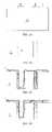
- FIGS. 1A to 1Dare schematic cross-sectional views showing steps of conformal deposition according to an embodiment of the present invention.
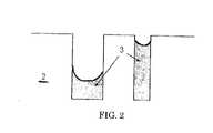
- FIG. 2is a schematic cross-sectional view showing steps of flow fill according to an embodiment of the present invention.
- FIGS. 3 and 4show FTIR spectra of multi-step, cured, insulative layers according to embodiments of the present invention, wherein FIG. 4 show the results of the multi-step curing without baking.
- FIGS. 5A and 5Bshow carbon levels of insulative layers with multi-step curing corresponding to the results shown in FIG. 3 .
- a flowable, insulative materialis used as a gap fill material, such as to fill a trench on a semiconductor substrate.
- the flowable, insulative materialis deposited into the trench to form an insulative layer, which includes residual carbon deposits.
- the semiconductor substratemay be a semiconductor wafer or other substrate comprising a layer of semiconductor material.
- semiconductor substrateincludes, but is not limited to, silicon wafers, silicon on insulator (SOI) substrates, silicon on sapphire substrates, epitaxial layers of silicon on a base semiconductor foundation, and other semiconductor materials such as silicon-germanium, germanium, gallium arsenide and indium phosphide.
- a semiconductor substrate 2may include a plurality of active regions 4 and a plurality of nonactive regions 6 .
- Active devicessuch as transistors, may be formed on the active regions 4 while at least one trench 8 ( FIG. 1B ) may be formed on the nonactive regions 6 to separate and isolate the active devices.
- the term “trench”is used in its broadest sense of a recess or cavity and is not to be construed as requiring any specific configuration or dimension. As such, the trench may be either a shallow trench or a deep trench. In another embodiment, the term “trench” may carry its ordinary and customary meaning.
- the trenches 8may be formed in the nonactive regions 6 of the semiconductor substrate 2 by any suitable techniques including conventional techniques, such as by masking and etching the semiconductor substrate 2 .
- additional layersmay be present on the semiconductor substrate 2 depending on the nature and/or its intended use of an ultimate semiconductor device structure that is to be formed.
- photoresist layers, pad oxide layers, and/or nitride layersmay be present on the semiconductor substrate 2 , in a manner known in the art, but are not shown for the sake of simplicity.
- an insulative layer 3is deposited conformably on the trenches 8 .
- the insulative layer 3may be deposited in such a way as to completely fill in a narrow trench (e.g., a width of 5 nm to 90 nm; an aspect ratio of 4 to 70) and be deposited conformably in a wide trench (e.g., a width of 90 nm to 700 nm; an aspect ratio of 0.5 to 4) as shown FIG. 1D .
- a narrow trenchhas a width of 3 nm to 30 nm and an aspect ratio of 4 to 15, and a wide trench has a width of 30 nm to 60 nm and an aspect ratio of 0.5 to 4.
- the conformal deposition process of FIGS. 1C-1Dis described in more detail below.
- the insulative layer 3also can completely or partially fill the trench by a vapor phase deposition process by controlling the amount of additives (e.g., hydrocarbon solvents such as benzene, toluene, n-hexane, cyclohexane and the like, or any two or more of the foregoing at an amount of 40 sccm to 400 sccm, or 400 sccm to 1600 sccm relative to the total gaseous precursor flow).
- the insulative layer 3may be deposited at a thickness ranging from approximately 50 ⁇ to 8000 ⁇ , including a thickness of approximately 300 ⁇ to 3000 ⁇ .
- the bottom-up deposition process of FIG. 2is described in more detail below.
- the insulative layermay be formed from a flowable oxide material that is deposited by, for example, plasma enhanced chemical vapor deposition (PECVD).
- PECVDplasma enhanced chemical vapor deposition
- the semiconductor substrate 2may be placed in a reaction chamber and gaseous precursors flow over the semiconductor substrate 2 and into the trench 8 .
- the gaseous precursorsmay include, but are not limited to, Si x H y and a solvent, or Si x H y and an organic silicon precursor, both of which are gaseous at, or near, a temperature at which the insulative layer 3 is deposited (Si x H y denoted one or more of any suitable silanes including Si x H 2n+2 ).
- the solventmay be one or more solvents selected from the group consisting of hydrocarbon solvents such as benzene, toluene, n-hexane, cyclohexane and the like, and ether solvents such as n-butyl ether, tetrahydrofuran, dioxane and the like. In this connection, however, any solvents may be used if such solvents are stable in or inert to the reaction system.
- the organic silicon precursormay be one or more precursors selected from the group consisting of silicon, carbon, hydrogen, nitrogen, and, optionally, oxygen.
- the organic silicon precursormay be an organosilane or an organosilazane.
- the organosilazanemay include, but is not limited to, a tetramethyldisilazane (TMDSZ), hexamethyl-cyclotrisilazane, octamethylcyclo-tetrasilazane. It is also contemplated that a mixture of two or more organic silicon precursors may be used. In an embodiment, a combination of organic silicon precursor and solvent can be used. Further, an inert gas such as N 2 , He, and/or Ar can be used. In the above, when the process gas does not contain nitrogen, a nitrogen-containing gas may be added.
- a silicon-containing gas, a nitrogen-containing gas, and a carbon-containing gasare used, provided that at least two different compounds constitute the silicon-containing gas, the nitrogen-containing gas, and the carbon-containing gas, such that relative ratios of film constituents in the feed gas can be modulated.
- Compounds that include a plurality of the depositing elementse.g., (CH 3 )SiN 3 can be used in certain embodiments.
- an oxidizing gassuch as O 2 or O 3 is added.
- no oxidizing gasis used.
- no inert gasis used.
- the formation of a deposition filmcan be controlled to result in conformal coating, whereas in a carbon rich condition, the formation of a depositing film can be controlled to result in vertical or bottom-up growth.
- a silicon source gas containing no nitrogen or carbon, a hydrocarbon solvent gas containing no nitrogen or silicon, and a nitrogen gas containing no silicon or carbonare used.
- a silicon source gas containing no nitrogen or carbon, an organo-silicon gas containing nitrogen, and a nitrogen source gas containing no silicon or carbonare used.
- the nitrogen-containing gas or nitrogen source gasN 2 , NH 3 , and/or NF 3 can be used.
- Organic Solvent40 to 1600 sccm (preferably 80 to 800 sccm)
- OSPOrganic Silicon Precursor
- Nitrogen Source Gas20 to 1000 sccm (preferably 50 to 500 sccm)
- Inert Gas300 to 2000 sccm (preferably 500 to 1000 sccm)
- Oxidizing Gas0 to 1000 sccm
- Temperature0 to 200° C. (preferably 0 to 50° C.)
- RF Power10 to 1000 W (preferably 50 to 500 W) at (430 kHz to 13.56 MHz)
- a deposition recipecan be provided with a ratio selected for conformal deposition, and by decreasing the aforementioned ratios related to the conformal recipe, a second, vertical deposition can be obtained.
- conformal depositionprecedes vertical or bottom-up deposition, such that both recipes can be used on a single substrate, with different effects on differently sized trenches or vias.
- the insulative layer 3 deposited by PECVDmay contain residual carbon deposits if the carbon contained in the organic silicon precursor or solvent is not completely oxidized during the PECVD process.
- the insulative layer 3may include up to approximately 30% carbon. The presence of carbon causes the insulative layer 3 to be soft and porous, which may lead to collapse of the insulative layer 3 under certain conditions.
- the carbonmay cause degradation in any semiconductor device structures that include the insulative material.
- the residual carbon depositsmay be removed from the insulative layer 3 by multi-step curing.
- the multi-step curingmay include oxygen-containing treatment, oxygen UV curing, and thermal annealing.
- the multi-step curingspecifically consists of the above in the listed sequence or order. These steps can be conducted consecutively or continuously.
- the curing sequencecan be useful for carbon-containing oxide films formed by the above PECVD processes, or for films formed by other processes (e.g., thermal CVD, spin-on deposition using liquid precursors, etc.).
- the oxygen-containing gasmay be introduced or arranged to flow into the reactor during baking so that residual carbon is released to a certain extent and the silicon-oxide structure is rearranged.
- the oxygen-containing gascan include, but is not limited to, O 2 , O 3 and/or N 2 O. Further, nitrogen gas or nitrogen-containing gas can be added.
- the semiconductor substrate 2may be maintained at a temperature ranging from approximately 100° C. to approximately 400° C. (including a range of 300 to 400° C.).
- Nitrogenmay be arranged to flow into the reaction chamber at a rate of at least 10 sccm and up to a rate of approximately 5,000 sccm (including a range of 100 to 3,000 sccm, or 500 to 2,000 sccm).
- Oxygenmay be arranged to flow into the reaction chamber at a rate of at least 10 sccm and up to a rate of approximately 10,000 sccm (including a range of 100 to 5,000 sccm, or 500 to 3,000 sccm).
- the oxygen-containing treatmentcomprises treating the conformal/flowable, insulative layer with nitrogen/oxygen, hydrogen/oxygen and/or H 2 O/oxygen steam at a temperature of between about 100° C. and about 400° C.
- the oxygen-containing treatmentcan be conducted at a pressure of 1 to 9 Torr for 5 to 20 minute.
- nitrogen and oxygenmay be introduced or arranged to flow into the reaction chamber while a UV lamp is ON so that reactive oxygen or ozone contacts the insulative layer 3 in the trench 8 for a sufficient amount of time to remove the residual carbon.
- the reactive oxygen or ozonemay permeate the layer and come into contact with the residual carbon deposits.
- the exposure of the insulative layer 3 to oxygen or ozonemay dramatically reduce the amount of residual carbon present in the insulative layer 3 from approximately 40 atomic % to less than approximately 1 atomic %.
- nitrogen or oxygenmay be introduced or arranged to flow into the reactor during annealing so that remaining impurities, such as —OH can be removed and the insulative layer 3 may be substantially free of impurities.
- the oxidizing gasO 2 , O 3 and/or N 2 O can be used.
- the semiconductor substrate 2may be maintained at a temperature ranging from approximately 0° C. to approximately 500° C. (including a range of 100 to 300° C.).
- Nitrogen gas or nitrogen-containing gasmay be arranged to flow into the reaction chamber at a rate of at least 10 sccm and up to a rate of approximately 5,000 sccm (including a range of 100 to 3,000 sccm, or 500 to 2,000 sccm).
- Oxygen gas or oxygen-containing gasmay be arranged to flow into the reaction chamber at a rate of at least 10 sccm and up to a rate of approximately 10,000 sccm (including a range of 100 to 5,000 sccm, or 500 to 3,000 sccm).
- the UV lampmay have a wavelength ranging from approximately 130 nm to approximately 400 nm with intensity of 50-200 mW/cm 2 .
- the insulative layer 3may be exposed to the UV for between approximately 5 seconds and approximately 1 hour (including range 2 minutes to 10 minutes) at a pressure of 2 Torr to 9 Torr. To improve the amount of carbon removed from the insulative layer 3 , the oxygen concentration and/or the UV irradiation time may be increased.
- nitrogen and oxygenare arranged to flow into the reaction chamber maintained with a susceptor temperature of approximately 400° C., at a rate of approximately 1,000 sccm and 3,000 sccm, respectively.
- the insulative layer 3may be exposed to the UV for as little as approximately 10 seconds.
- the semiconductor substrate 2may be maintained at a temperature ranging from approximately 100° C. to approximately 500° C. (including a range of 300 to 450° C.).
- the semiconductor substrate 2may be maintained at 400° C.
- Nitrogen gas or nitrogen-containing gasmay be arranged to flow into the reaction chamber at a rate of at least 10 standard cubic centimeters per minute (sccm) and up to a rate of approximately 5,000 sccm (including a range of 100 to 3,000 sccm, or 500 to 2,000 sccm).
- Oxygen gas or oxygen-containing gasmay be arranged to flow into the reaction chamber at a rate of at least 10 sccm and up to a rate of approximately 10,000 sccm (including a range of 100 to 5,000 sccm, or 500 to 3,000 sccm).
- an insulative layer 3was formed by introducing SiH 4 , n-hexane and nitrogen gas into a reaction chamber for CVD processing wherein a semiconductor substrate 2 having trenches 8 was placed.
- the trenchesincluded relatively wide trenches (a width of 500 m and a depth of 350 nm) and relatively narrow trenches (a width of 50 nm and a depth of 350 nm).
- the flow rates of SiH 4 , n-hexane, and nitrogen gasare shown in Table 1. No oxidizing gas was used.
- RF power(a frequency of 13.56 MHz, 200 W) was applied to generate plasma over the substrate 2 .
- the semiconductor substrate 2may be maintained at a temperature ranging from approximately 0° C. to 200° C. by placing the semiconductor substrate 2 on a chuck maintained at that temperature. In this example, the semiconductor substrate 2 was maintained at a temperature of approximately 30° C.
- the reaction chambermay be maintained at a pressure ranging from approximately 2 Torr to approximately 10 Torr (in this example, at approximately 3 Torr).
- the thickness of the deposited filmwas from 30 nm to 300 nm. After completion of the deposition, the trenches were observed with a scanning electron microscope.
- the process conditions and the formation type of resultant insulative layerare indicated in Table 1. As shown in Table 1, the hydrocarbon flow rate (n-hexane) relative to the silicon flow rate (SiH 4 ) and the nitrogen flow rate (N 2 ) affects the formation type of depositing film.
- An insulative layer 3was formed by introducing SiH 4 , TMDSZ and NH 3 into a reaction chamber for CVD processing wherein a semiconductor substrate 2 having trenches 8 was placed.
- the trenchesincluded relatively wide trenches (a width of 500 nm and a depth of 350 nm) and relatively narrow trenches (a width of 50 nm and a depth of 350 nm).
- the flow rates of SiH 4 , n-hexane, and nitrogen gasare shown in Table 2. No oxidizing gas was used.
- RF power(a frequency of 13.56 MHz, 200 W) was applied to generate plasma over the substrate 2 .
- the SiH 4 and TMDSZreacted in the presence of the NH 3 gas on the surface of the semiconductor substrate 2 having the trenches 8 to form the insulative layer 3 .
- the semiconductor substrate 2may be maintained at a temperature ranging from approximately 0° C. to 200° C. by placing the semiconductor substrate 2 on a chuck maintained at that temperature. In this example, the semiconductor substrate 2 may be maintained at a temperature of approximately 30° C.
- the reaction chambermay be maintained at a pressure ranging from approximately 2 Torr to approximately 10 Torr (in this example, at approximately 5 Torr).
- the thickness of the deposited filmwas from 30 nm to 300 nm. After completion of the deposition, the trenches were observed with a scanning electron microscope.
- the process conditions and the formation type of resultant insulative layerare indicated in Table 2. As shown in Table 2, the TMDSZ flow rate relative to the SiH 4 flow rate and the NH 3 flow rate affects the formation type of depositing film.
- TMDSZAs compared to the flow rate of SiH 4 (a ratio of TMDSZ/SiH 4 is less than 1.0), a limited quantity of organosilazane molecules in the plasma saturates the dissociation reaction and recombination reaction. This restricts the surface diffusion and; consequently, a conformal insulative film is likely to be formed.
- the ratio of TMDSZ/SiH 4is 1.0 and over, complete or partial (bottom-up) filling is more likely to be formed.
- the ratio of TMDSZ/NH 3is also a parameter controlling the formation type.
- the ratio of NH 3 /SiH 4is also a parameter controlling the formation type in a different direction.
- the insulative layers 3were deposited on a blanket wafer by PECVD at 30° C. according to the processes described in Example 1.
- the multi-step curingwas comprised of oxygen-containing treatment (baking), oxygen UV curing, and thermal annealing, which were conducted as follows:
- UV lampXe lamp (100 mW/cm 2 )
- FIGS. 3 and 4are Fourier-transform infrared absorption spectra (FTIR) analysis of insulative layers 3 deposited as described above.
- FIG. 3shows the as-deposited results, as well as the results of sequential treatments consisting essentially of the baking, UV curing, and thermal annealing, in sequence
- FIG. 4shows the as-deposited results, as well as the results of sequential treatments consisting essentially of the oxygen UV curing and annealing (i.e., no baking).
- FTIRFourier-transform infrared absorption spectra
- the insulative layers that were baked and UV exposedhad significantly reduced ( FIG. 3 ) amounts of carbon (at a wave number of about 2,800 cm ⁇ 1 ⁇ 3,000 cm ⁇ 1 ) as compared to the insulative layers that were just UV exposed for the same amount of time ( FIG. 4 ).
- FIGS. 5A and 5Bshow nuclear reaction analysis (NRA) results of multi-step curing consisting essentially of the baking, UV irradiation and annealing in sequence (corresponding to FIG. 3 ).
- FIG. 5Bis a detailed view of FIG. 5A , enlarging the lower yield ranges.
- concentrations of hydrogen, carbon, nitrogen, oxygen and siliconis 3.7% (atomic %), 1.0% (atomic %), 0.4% (atomic %), 64.1% (atomic %) and 30.8% (atomic %), respectively.
- the carbon contentcan drastically be reduced.
- a method of forming a conformal and/or flowable, insulative layer on intermediate semiconductor device structurecomprising: providing a conformal and/or flowable, insulative layer comprising silicon, carbon, hydrogen, nitrogen, oxygen or a combination of two or more thereof, and providing a semiconductor substrate comprising at least one trench; forming an insulative layer in the at least one trench; depositing a conformal and/or flowable, insulative layer at least one trench by plasma enhanced chemical vapor deposition.
- a method of removing residual carbon deposits from conformal and/or flowable, insulative layercomprising: providing a conformal and/or flowable, insulative layer comprising silicon, carbon, hydrogen, nitrogen, oxygen or a combination of two or more thereof, and treating the conformal and/or flowable, insulative layer under multi-step cures that consist essentially of an oxygen-containing treatment, a UV irradiation and annealing in sequence to remove residual carbon deposits from the conformal and/or flowable, insulative layer.
- UV irradiationcomprises UV irradiation treating the conformal and/or flowable, insulative layer with wave length ranging between approximately 130 nm and approximately 400 nm.
- a method of treating an intermediate semiconductor device structure to remove carbon depositscomprising; providing a semiconductor substrate comprising at least one trench; depositing a flowable oxide material in the at least one trench; and introducing multi-step cures that consists essentially oxygen-containing treatment, UV irradiation and annealing in sequence to remove residual carbon deposits present in the flowable oxide material.
- depositing a flowable oxide material in the at least one trenchcomprises depositing the flowable oxide material comprising silicon, nitride, carbon, hydrogen, oxygen or combination of two or more thereof in the at least one trench.
- the method of 22), wherein forming an insulative layer by plasma enhanced chemical vapor depositioncomprises introducing an organic silicon precursor and an oxidizing agent over the semiconductor substrate.
- UV irradiationcomprises UV irradiation treating the insulative layer with wave length ranging between approximately 130 nm and approximately 400 nm.
Landscapes
- Engineering & Computer Science (AREA)
- Physics & Mathematics (AREA)
- Condensed Matter Physics & Semiconductors (AREA)
- General Physics & Mathematics (AREA)
- Manufacturing & Machinery (AREA)
- Computer Hardware Design (AREA)
- Microelectronics & Electronic Packaging (AREA)
- Power Engineering (AREA)
- Formation Of Insulating Films (AREA)
- Element Separation (AREA)
Abstract
Description
- 1. Field of the Invention
- The present invention relates to the field of semiconductor integrated circuit manufacturing and, more particularly to a method of forming device isolation regions on a semiconductor substrate by using PECVD and to a method of removing residual carbon deposits from an intermediate semiconductor device structure.
- 2. Description of the Related Art
- Integrated circuits fabricated on semiconductor substrates for large scale integration require multiple levels of metal interconnections to electrically interconnect the discrete layers of semiconductor devices on the semiconductor chips. Today several million devices can be fabricated in a single chip, for example, the mega-bit memory chips which are commonly used today in personal mobile and in other applications.
- Devices of semiconductor typically include semiconductor substrate and a plurality of adjacent, active devices that are electrically isolated from one another. With the increased circuit density, effective isolation between active devices becomes increasingly important. One isolation technique is local oxidation of silicon isolation (LOCOS), which forms a recessed oxide layer in non-active regions of the semiconductor substrate to isolate the active devices. The oxide layer is conventionally formed by patterning a hard mask and thermal oxidation of the substrate.
- The above described conventional LOCOS technique has a number of disadvantages, which become rather unacceptable when attempting to apply this technique to the fabrication of sub-micron devices. First, the oxidization of silicon happens not only in the vertical direction but also in the horizontal direction. As a result, a part of the field oxide grows under adjacent silicon nitride or other hard mask layers and lifts it up. This is termed the “bird's beak effect” by persons skilled in the art. Secondly, due to the stresses caused by the bird's beak effect, a part of nitride hard mask in the compressed regions of silicon nitride layer diffuses to adjacent tensile strained regions at the interface of the pad oxide layer and the substrate, and forms a silicon-nitride-like region. In subsequent process steps of forming gate oxides, due to the mask effect of the silicon-nitride-like layer, the gate oxides will be thinner than they should be. This is termed the “white ribbon effect” because a white ribbon will appear at the edges of active regions under optical microscopes.
- An alternative technique is trench isolation, which involves etching trenches in nonactive regions of a semiconductor substrate. Trench isolation is referred to as shallow trench isolation (STI) or deep trench isolation (DTI), depending on the depth of the trench etched in the semiconductor substrate. DTI structures, which typically have a depth of greater than approximately 3 microns, are used to isolate active devices such as N-wells and P-wells. Shallow trench structures are used to isolate adjacent electronic devices, such as transistors, and often have a depth of less than approximately 1 micron. The trenches are filled with a deposited insulative dielectric material, such as a silicon dioxide material. The filled trenches are known in the art as trench isolation or trench isolation regions. The trench is typically filled with the silicon dioxide material by a chemical vapor deposition (CVD) technique, such as high density plasma CVD. In CVD, gaseous precursors of the silicon dioxide material are supplied to a surface of the semiconductor substrate. The gaseous precursors react with the surface to form a film or layer of the silicon dioxide material.
- Trench isolation provides a smaller isolation area and better surface planarization than LOCOS. While trench isolation provides these advantages, undesirable voids can be formed in the silicon dioxide material as the trench fills because the silicon dioxide material tends to stick to the sides and sidewalls of the trench, rather than evenly filling the trench from the bottom to the top. Voids are especially common in deep trenches, such as trenches having a high aspect ratio (depth:width) of greater than approximately 3:1. Voids also commonly form at later stages of the filling process because the trenches, both deep and shallow, become narrower as they fill.
- Recently, CVD of flowable oxide material has been developed to reduce the formation of voids. An organic doped silicon oxide film is formed in trenches by supplying a liquid silicon precursor which includes a methyl or ethyl group bond. Often the precursor is supplied while spinning the substrate, such that the resultant process or material is referred to as SOD for spin-on deposition or spin-on dielectric. Furthermore, as the technology shrinks nodes to 45 nm and beyond, the demands for not only gap-filling, but also conformal coating are ever increasing.
- In addition, while depositing the flowable oxide material, residual carbon deposits are present in the deposited film if the precursors contain carbon. Carbon in the deposited film causes the film to be soft and porous, which makes the deposited film unstable during subsequent processing, such as etching processes. Also, if the flowable oxide material is used to fill isolation trenches within the semiconductor substrate, the carbon cause device degradation.
- An object of the disclosed embodiments of the present invention, among other objects, is to provide a method of forming device isolation for an integrated circuit and to provide a method of removing residual carbon deposits at low temperatures (e.g., <500° C.). The methods described herein provide control over both filling and conformal coating in trenches. In an embodiment, this method comprises: providing a flowable, insulative material comprising silicon, carbon, nitrogen, hydrogen, oxygen or any combination of two or more thereof; and forming a thin insulative layer, by using the flowable, insulative material, in a trench located on a semiconductor substrate. The method allow deposition wherein the flowable, insulative material grows in a conformal manner in a silicon and nitrogen rich condition, whereas in a carbon rich condition, the flowable, insulative material grows in trenches vertically from the bottom of the trenches, without lateral deposition. By such methods, field insulative materials (preferably of substantially the same thickness) can be formed in trenches of different sizes. In another embodiment, the method further comprises removing residual carbon deposits from the flowable, insulative material by multi-step curing, such as oxygen-containing treatment at a temperature of between approximately 100° C. and 500° C., ozone exposure by UV curing, followed by thermal annealing at a temperature of between approximately 100° C. and 500° C. in a non-oxidizing atmosphere of, e.g., N2.
- For purposes of summarizing aspects of the invention and the advantages achieved over the related art, certain objects and advantages of the invention are described in this disclosure. Of course, it is to be understood that not necessarily all such objects or advantages may be achieved in accordance with any particular embodiment of the invention. Thus, for example, those skilled in the art will recognize that the invention may be embodied or carried out in a manner that achieves or optimizes one advantage or group of advantages as taught herein without necessarily achieving other objects or advantages as may be taught or suggested herein.
- Further aspects, features and advantages of this invention will become apparent from the detailed description of the preferred embodiments which follow.
- These and other features of this invention will now be described with reference to the drawings of preferred embodiments which are intended to illustrate and not to limit the invention. The drawings are oversimplified for illustrative purposes and are not to scale.
FIGS. 1A to 1D are schematic cross-sectional views showing steps of conformal deposition according to an embodiment of the present invention.FIG. 2 is a schematic cross-sectional view showing steps of flow fill according to an embodiment of the present invention.FIGS. 3 and 4 show FTIR spectra of multi-step, cured, insulative layers according to embodiments of the present invention, whereinFIG. 4 show the results of the multi-step curing without baking.FIGS. 5A and 5B show carbon levels of insulative layers with multi-step curing corresponding to the results shown inFIG. 3 .- In an embodiment, a flowable, insulative material is used as a gap fill material, such as to fill a trench on a semiconductor substrate. The flowable, insulative material is deposited into the trench to form an insulative layer, which includes residual carbon deposits. The semiconductor substrate may be a semiconductor wafer or other substrate comprising a layer of semiconductor material. As used herein, the term “semiconductor substrate” includes, but is not limited to, silicon wafers, silicon on insulator (SOI) substrates, silicon on sapphire substrates, epitaxial layers of silicon on a base semiconductor foundation, and other semiconductor materials such as silicon-germanium, germanium, gallium arsenide and indium phosphide.
- The disclosed embodiments of the present invention will be explained with reference to drawings and preferred embodiments. However, the drawings and preferred embodiments are not intended to limit the present invention.
- As shown in
FIG. 1A , asemiconductor substrate 2 may include a plurality of active regions4 and a plurality of nonactive regions6. Active devices, such as transistors, may be formed on the active regions4 while at least one trench8 (FIG. 1B ) may be formed on the nonactive regions6 to separate and isolate the active devices. In this embodiment, the term “trench” is used in its broadest sense of a recess or cavity and is not to be construed as requiring any specific configuration or dimension. As such, the trench may be either a shallow trench or a deep trench. In another embodiment, the term “trench” may carry its ordinary and customary meaning. - As presented in
FIG. 1B , the trenches8 may be formed in the nonactive regions6 of thesemiconductor substrate 2 by any suitable techniques including conventional techniques, such as by masking and etching thesemiconductor substrate 2. As is known in the art, additional layers may be present on thesemiconductor substrate 2 depending on the nature and/or its intended use of an ultimate semiconductor device structure that is to be formed. For the sake of example only, photoresist layers, pad oxide layers, and/or nitride layers may be present on thesemiconductor substrate 2, in a manner known in the art, but are not shown for the sake of simplicity. - As shown
FIG. 1C , aninsulative layer 3 is deposited conformably on the trenches8. Theinsulative layer 3 may be deposited in such a way as to completely fill in a narrow trench (e.g., a width of 5 nm to 90 nm; an aspect ratio of 4 to 70) and be deposited conformably in a wide trench (e.g., a width of 90 nm to 700 nm; an aspect ratio of 0.5 to 4) as shownFIG. 1D . - In another embodiment, a narrow trench has a width of 3 nm to 30 nm and an aspect ratio of 4 to 15, and a wide trench has a width of 30 nm to 60 nm and an aspect ratio of 0.5 to 4. The conformal deposition process of
FIGS. 1C-1D is described in more detail below. - Referring to
FIG. 2 , theinsulative layer 3 also can completely or partially fill the trench by a vapor phase deposition process by controlling the amount of additives (e.g., hydrocarbon solvents such as benzene, toluene, n-hexane, cyclohexane and the like, or any two or more of the foregoing at an amount of 40 sccm to 400 sccm, or 400 sccm to 1600 sccm relative to the total gaseous precursor flow). Theinsulative layer 3 may be deposited at a thickness ranging from approximately 50 Å to 8000 Å, including a thickness of approximately 300 Å to 3000 Å. The bottom-up deposition process ofFIG. 2 is described in more detail below. - In an embodiment, the insulative layer may be formed from a flowable oxide material that is deposited by, for example, plasma enhanced chemical vapor deposition (PECVD). The
semiconductor substrate 2 may be placed in a reaction chamber and gaseous precursors flow over thesemiconductor substrate 2 and into the trench8. The gaseous precursors may include, but are not limited to, SixHyand a solvent, or SixHyand an organic silicon precursor, both of which are gaseous at, or near, a temperature at which theinsulative layer 3 is deposited (SixHydenoted one or more of any suitable silanes including SixH2n+2). Examples of the solvent may be one or more solvents selected from the group consisting of hydrocarbon solvents such as benzene, toluene, n-hexane, cyclohexane and the like, and ether solvents such as n-butyl ether, tetrahydrofuran, dioxane and the like. In this connection, however, any solvents may be used if such solvents are stable in or inert to the reaction system. The organic silicon precursor may be one or more precursors selected from the group consisting of silicon, carbon, hydrogen, nitrogen, and, optionally, oxygen. For instance, the organic silicon precursor may be an organosilane or an organosilazane. The organosilazane may include, but is not limited to, a tetramethyldisilazane (TMDSZ), hexamethyl-cyclotrisilazane, octamethylcyclo-tetrasilazane. It is also contemplated that a mixture of two or more organic silicon precursors may be used. In an embodiment, a combination of organic silicon precursor and solvent can be used. Further, an inert gas such as N2, He, and/or Ar can be used. In the above, when the process gas does not contain nitrogen, a nitrogen-containing gas may be added. - In embodiments, a silicon-containing gas, a nitrogen-containing gas, and a carbon-containing gas are used, provided that at least two different compounds constitute the silicon-containing gas, the nitrogen-containing gas, and the carbon-containing gas, such that relative ratios of film constituents in the feed gas can be modulated. Compounds that include a plurality of the depositing elements (e.g., (CH3)SiN3can be used in certain embodiments. In an embodiment, an oxidizing gas such as O2or O3is added. In another embodiment, no oxidizing gas is used. In an embodiment, no inert gas is used. By adjusting the flow rate of each gas, it is possible to control the formation of a depositing film: In a silicon and/or nitrogen rich condition, the formation of a deposition film can be controlled to result in conformal coating, whereas in a carbon rich condition, the formation of a depositing film can be controlled to result in vertical or bottom-up growth.
- In an embodiment, a silicon source gas containing no nitrogen or carbon, a hydrocarbon solvent gas containing no nitrogen or silicon, and a nitrogen gas containing no silicon or carbon are used. In another embodiment, a silicon source gas containing no nitrogen or carbon, an organo-silicon gas containing nitrogen, and a nitrogen source gas containing no silicon or carbon are used. As the nitrogen-containing gas or nitrogen source gas, N2, NH3, and/or NF3can be used.
- Deposition conditions in embodiments may be as follows:
- SixHy(SiH): 5 to 200 sccm (preferably 10 to 100 sccm)
- Organic Solvent (OS): 40 to 1600 sccm (preferably 80 to 800 sccm)
- Organic Silicon Precursor (OSP): 10 to 400 sccm (preferably 20 to 200 sccm)
- Nitrogen Source Gas (NSG): 20 to 1000 sccm (preferably 50 to 500 sccm)
- Inert Gas (IG): 300 to 2000 sccm (preferably 500 to 1000 sccm)
- Oxidizing Gas: 0 to 1000 sccm
- Flow Ratio of OS/SiH: 0.2 to 320 (preferably 2 to 10)
- Flow Ratio of OSP/SiH: 0.05 to 80 (preferably 0.5 to 3)
- Flow Ratio of (OS or OSP)/NSG: 0.01 to 80 (preferably 0.1 to 2.0)
- Temperature: 0 to 200° C. (preferably 0 to 50° C.)
- Pressure: 0.1 to 10 Torr (preferably 1 to 5 Torr)
- RF Power: 10 to 1000 W (preferably 50 to 500 W) at (430 kHz to 13.56 MHz)
- In the above, by adjusting the flow ratios of (OS or OSP)/SiH, NSG/SiH, and/or (OS or OSP)/NSG, it is possible to control the formation of a depositing film between conformal coating and vertical growth. For example, if conformal coating is preferable over vertical growth, the ratio of (OS or OSP)/SiH and/or (OS or OSP)/NSG is increased; if vertical growth is preferable over conformal coating, the ratio of (OS or OSP)/SiH and/or (OS or OSP)/NSG is decreased. Thus a deposition recipe can be provided with a ratio selected for conformal deposition, and by decreasing the aforementioned ratios related to the conformal recipe, a second, vertical deposition can be obtained. In some embodiments, conformal deposition precedes vertical or bottom-up deposition, such that both recipes can be used on a single substrate, with different effects on differently sized trenches or vias.
- The
insulative layer 3 deposited by PECVD may contain residual carbon deposits if the carbon contained in the organic silicon precursor or solvent is not completely oxidized during the PECVD process. Theinsulative layer 3 may include up to approximately 30% carbon. The presence of carbon causes theinsulative layer 3 to be soft and porous, which may lead to collapse of theinsulative layer 3 under certain conditions. In addition, when theinsulative layer 3 is used to fill trenches, the carbon may cause degradation in any semiconductor device structures that include the insulative material. - In an embodiment, the residual carbon deposits may be removed from the
insulative layer 3 by multi-step curing. The multi-step curing may include oxygen-containing treatment, oxygen UV curing, and thermal annealing. In an embodiment, the multi-step curing specifically consists of the above in the listed sequence or order. These steps can be conducted consecutively or continuously. The curing sequence can be useful for carbon-containing oxide films formed by the above PECVD processes, or for films formed by other processes (e.g., thermal CVD, spin-on deposition using liquid precursors, etc.). - First, during the oxygen-containing treatment, the oxygen-containing gas may be introduced or arranged to flow into the reactor during baking so that residual carbon is released to a certain extent and the silicon-oxide structure is rearranged. The oxygen-containing gas can include, but is not limited to, O2, O3and/or N2O. Further, nitrogen gas or nitrogen-containing gas can be added.
- During the oxygen-containing treatment, which is also referred to as baking (without UV irradiation), the
semiconductor substrate 2 may be maintained at a temperature ranging from approximately 100° C. to approximately 400° C. (including a range of 300 to 400° C.). Nitrogen may be arranged to flow into the reaction chamber at a rate of at least 10 sccm and up to a rate of approximately 5,000 sccm (including a range of 100 to 3,000 sccm, or 500 to 2,000 sccm). Oxygen may be arranged to flow into the reaction chamber at a rate of at least 10 sccm and up to a rate of approximately 10,000 sccm (including a range of 100 to 5,000 sccm, or 500 to 3,000 sccm). In an embodiment, the oxygen-containing treatment comprises treating the conformal/flowable, insulative layer with nitrogen/oxygen, hydrogen/oxygen and/or H2O/oxygen steam at a temperature of between about 100° C. and about 400° C. The oxygen-containing treatment can be conducted at a pressure of 1 to 9 Torr for 5 to 20 minute. - Second, during the oxygen UV curing, nitrogen and oxygen may be introduced or arranged to flow into the reaction chamber while a UV lamp is ON so that reactive oxygen or ozone contacts the
insulative layer 3 in the trench8 for a sufficient amount of time to remove the residual carbon. The reactive oxygen or ozone may permeate the layer and come into contact with the residual carbon deposits. Although the following theory is not intended to limit the present invention, it is believed that the oxygen or ozone oxidizes the residual carbon deposits to produce volatile carbon species, such as carbon monoxide or carbon dioxide. These volatile carbon species subsequently diffuse out of theinsulative layer 3. The exposure of theinsulative layer 3 to oxygen or ozone may dramatically reduce the amount of residual carbon present in theinsulative layer 3 from approximately 40 atomic % to less than approximately 1 atomic %. Subsequently, nitrogen or oxygen may be introduced or arranged to flow into the reactor during annealing so that remaining impurities, such as —OH can be removed and theinsulative layer 3 may be substantially free of impurities. As the oxidizing gas, O2, O3and/or N2O can be used. - For oxygen UV curing, the
semiconductor substrate 2 may be maintained at a temperature ranging from approximately 0° C. to approximately 500° C. (including a range of 100 to 300° C.). Nitrogen gas or nitrogen-containing gas may be arranged to flow into the reaction chamber at a rate of at least 10 sccm and up to a rate of approximately 5,000 sccm (including a range of 100 to 3,000 sccm, or 500 to 2,000 sccm). Oxygen gas or oxygen-containing gas may be arranged to flow into the reaction chamber at a rate of at least 10 sccm and up to a rate of approximately 10,000 sccm (including a range of 100 to 5,000 sccm, or 500 to 3,000 sccm). The UV lamp may have a wavelength ranging from approximately 130 nm to approximately 400 nm with intensity of 50-200 mW/cm2. Theinsulative layer 3 may be exposed to the UV for between approximately 5 seconds and approximately 1 hour (includingrange 2 minutes to 10 minutes) at a pressure of 2 Torr to 9 Torr. To improve the amount of carbon removed from theinsulative layer 3, the oxygen concentration and/or the UV irradiation time may be increased. - In an embodiment, during the UV curing, nitrogen and oxygen are arranged to flow into the reaction chamber maintained with a susceptor temperature of approximately 400° C., at a rate of approximately 1,000 sccm and 3,000 sccm, respectively. To remove the residual carbon, the
insulative layer 3 may be exposed to the UV for as little as approximately 10 seconds. - During the thermal annealing, the
semiconductor substrate 2 may be maintained at a temperature ranging from approximately 100° C. to approximately 500° C. (including a range of 300 to 450° C.). For the sake of example only, thesemiconductor substrate 2 may be maintained at 400° C. Nitrogen gas or nitrogen-containing gas may be arranged to flow into the reaction chamber at a rate of at least 10 standard cubic centimeters per minute (sccm) and up to a rate of approximately 5,000 sccm (including a range of 100 to 3,000 sccm, or 500 to 2,000 sccm). Oxygen gas or oxygen-containing gas may be arranged to flow into the reaction chamber at a rate of at least 10 sccm and up to a rate of approximately 10,000 sccm (including a range of 100 to 5,000 sccm, or 500 to 3,000 sccm). - The disclosed embodiments of the present invention will be more precisely described with reference to preferred examples, which should not be construed as examples limiting the present invention.
- In the present disclosure where conditions and/or structures are not specified, the skilled artisan is the art can readily provide such conditions and/or structures, in view of the present disclosure, as a matter of routine experimentation. Also, in the present disclosure, the numerical numbers applied in embodiments can be modified in other embodiments (e.g., by expanding the disclosed ranges by ±50%), and the ranges applied in embodiments may include or exclude the endpoints.
- With reference to the features of
FIGS. 1 and 2 , aninsulative layer 3 was formed by introducing SiH4, n-hexane and nitrogen gas into a reaction chamber for CVD processing wherein asemiconductor substrate 2 having trenches8 was placed. The trenches included relatively wide trenches (a width of 500 m and a depth of 350 nm) and relatively narrow trenches (a width of 50 nm and a depth of 350 nm). The flow rates of SiH4, n-hexane, and nitrogen gas are shown in Table 1. No oxidizing gas was used. RF power (a frequency of 13.56 MHz, 200 W) was applied to generate plasma over thesubstrate 2. The SiH4and solvent reacted in the presence of the inert gas on the surface of thesemiconductor substrate 2 having the trenches8 to form theinsulative layer 3. Thesemiconductor substrate 2 may be maintained at a temperature ranging from approximately 0° C. to 200° C. by placing thesemiconductor substrate 2 on a chuck maintained at that temperature. In this example, thesemiconductor substrate 2 was maintained at a temperature of approximately 30° C. The reaction chamber may be maintained at a pressure ranging from approximately 2 Torr to approximately 10 Torr (in this example, at approximately 3 Torr). The thickness of the deposited film (as measured on a flat surface) was from 30 nm to 300 nm. After completion of the deposition, the trenches were observed with a scanning electron microscope. - The process conditions and the formation type of resultant insulative layer are indicated in Table 1. As shown in Table 1, the hydrocarbon flow rate (n-hexane) relative to the silicon flow rate (SiH4) and the nitrogen flow rate (N2) affects the formation type of depositing film.
TABLE 1 SiH4 Hexane N2 Hexane/ N2/ Hexane/ Example (sccm) (sccm) (sccm) SiH4 SiH4 N2 Insulative layer 1-1 50 400 500 8 10 0.8 vertical filling 1-2 50 285 500 5.7 10 0.57 Conformal + filling in narrow pattern 1-3 50 200 500 4 10 0.4 Conformal + filling in narrow pattern 1-4 50 150 500 3 10 0.3 Conformal - With a small hydrocarbon flow rate as compared to the SiH4flow rate (a ratio of hexane/SiH4of less then 8), a limited quantity of hydrocarbon molecules in the plasma saturated the dissociation reaction and recombination reaction. This restricts the surface diffusion and; consequently, a conformal insulative film is more likely to be formed. On the other hand, when the ratio of hexane/SiH4is 8 and over, a complete or partial bottom-up or vertical filling is more likely to be formed. As with the ratio of hexane/SiH4, the ratio of hexane/N2is also a parameter controlling the formation type.
- An
insulative layer 3 was formed by introducing SiH4, TMDSZ and NH3into a reaction chamber for CVD processing wherein asemiconductor substrate 2 having trenches8 was placed. The trenches included relatively wide trenches (a width of 500 nm and a depth of 350 nm) and relatively narrow trenches (a width of 50 nm and a depth of 350 nm). The flow rates of SiH4, n-hexane, and nitrogen gas are shown in Table 2. No oxidizing gas was used. RF power (a frequency of 13.56 MHz, 200 W) was applied to generate plasma over thesubstrate 2. The SiH4and TMDSZ reacted in the presence of the NH3gas on the surface of thesemiconductor substrate 2 having the trenches8 to form theinsulative layer 3. Thesemiconductor substrate 2 may be maintained at a temperature ranging from approximately 0° C. to 200° C. by placing thesemiconductor substrate 2 on a chuck maintained at that temperature. In this example, thesemiconductor substrate 2 may be maintained at a temperature of approximately 30° C. The reaction chamber may be maintained at a pressure ranging from approximately 2 Torr to approximately 10 Torr (in this example, at approximately 5 Torr). The thickness of the deposited film (as measured on a flat surface) was from 30 nm to 300 nm. After completion of the deposition, the trenches were observed with a scanning electron microscope. - The process conditions and the formation type of resultant insulative layer are indicated in Table 2. As shown in Table 2, the TMDSZ flow rate relative to the SiH4flow rate and the NH3flow rate affects the formation type of depositing film.
- With a small flow rate of TMDSZ as compared to the flow rate of SiH4(a ratio of TMDSZ/SiH4is less than 1.0), a limited quantity of organosilazane molecules in the plasma saturates the dissociation reaction and recombination reaction. This restricts the surface diffusion and; consequently, a conformal insulative film is likely to be formed. On the other hand, the ratio of TMDSZ/SiH4is 1.0 and over, complete or partial (bottom-up) filling is more likely to be formed. As with the ratio of TMDSZ/SiH4, the ratio of TMDSZ/NH3is also a parameter controlling the formation type. The ratio of NH3/SiH4is also a parameter controlling the formation type in a different direction.
TABLE 2 SiH4 TMDSZ NH3 TMDSZ/ NH3/ TMDSZ/ Example (sccm) (sccm) (sccm) SiH4 SiH4 NH3 Insulative layer 2-1 40 80 50 2 1.25 1.6 Vertical filling 2-2 40 40 50 1 1.25 0.8 Vertical filling 2-3 40 20 50 0.5 1.25 0.4 Conformal + filling in narrow pattern 2-4 40 20 100 0.5 2.5 0.2 Conformal + filling in narrow pattern 2-5 40 20 200 0.5 5 0.1 Conformal - The skilled artisan will appreciate that based on the device isolation technology described herein, appropriate gases and their flow ratios can be determined and modified for the target formation type of depositing film (conformal coating or vertical growth). Different types of deposition can thus be achieved using the same deposition equipment and even the same precursors.
- To determine the chemical bonding and compositions of multi-step cured insulative layers, the
insulative layers 3 were deposited on a blanket wafer by PECVD at 30° C. according to the processes described in Example 1. The multi-step curing was comprised of oxygen-containing treatment (baking), oxygen UV curing, and thermal annealing, which were conducted as follows: - Baking:
- Oxygen gas: 3 slm
- Nitrogen gas: 1 slm
- Temperature: 400° C.
- Duration: 1 minute
- Pressure: 800 Pa
- UV Curing:
- UV lamp: Xe lamp (100 mW/cm2)
- Oxygen gas: 3 slm
- Nitrogen gas: 1 slm
- Temperature: 430° C.
- Duration: 2 minutes
- Pressure: 1200 Pa
- Thermal Annealing:
- Oxygen gas: 3 slm
- Nitrogen gas: 1 slm
- Temperature: 430° C.
- Duration: 30 minutes
- Pressure: 800 Pa
FIGS. 3 and 4 are Fourier-transform infrared absorption spectra (FTIR) analysis ofinsulative layers 3 deposited as described above.FIG. 3 shows the as-deposited results, as well as the results of sequential treatments consisting essentially of the baking, UV curing, and thermal annealing, in sequence, whereasFIG. 4 shows the as-deposited results, as well as the results of sequential treatments consisting essentially of the oxygen UV curing and annealing (i.e., no baking).- As shown
FIGS. 3 and 4 , the insulative layers that were baked and UV exposed had significantly reduced (FIG. 3 ) amounts of carbon (at a wave number of about 2,800 cm−1˜3,000 cm−1) as compared to the insulative layers that were just UV exposed for the same amount of time (FIG. 4 ). FIGS. 5A and 5B show nuclear reaction analysis (NRA) results of multi-step curing consisting essentially of the baking, UV irradiation and annealing in sequence (corresponding toFIG. 3 ).FIG. 5B is a detailed view ofFIG. 5A , enlarging the lower yield ranges. As shown inFIGS. 5A and 5B , concentrations of hydrogen, carbon, nitrogen, oxygen and silicon is 3.7% (atomic %), 1.0% (atomic %), 0.4% (atomic %), 64.1% (atomic %) and 30.8% (atomic %), respectively. By using a combination of the baking, UV irradiation, and thermal annealing, the carbon content can drastically be reduced.- The present invention includes the above mentioned embodiments and other various embodiments including the following:
- 1) A method of forming a conformal and/or flowable, insulative layer on intermediate semiconductor device structure, comprising: providing a conformal and/or flowable, insulative layer comprising silicon, carbon, hydrogen, nitrogen, oxygen or a combination of two or more thereof, and providing a semiconductor substrate comprising at least one trench; forming an insulative layer in the at least one trench; depositing a conformal and/or flowable, insulative layer at least one trench by plasma enhanced chemical vapor deposition.
- 2) The method of 1), wherein forming an insulative layer in the at least one trench comprises depositing a conformal and/or flowable, insulative material comprising silicon, carbon, hydrogen, nitrogen, oxygen or a combination of two or more thereof in the at least one trench.
- 3) The method of 2), wherein depositing a conformal and/or flowable, insulative material comprising silicon, carbon, hydrogen, nitrogen, oxygen or a combination of two or more thereof in the at least one trench comprises conformal depositing in the at least one trench with the conformal and/or flowable, insulative material by controlling an amount of silicon, carbon, hydrogen, and nitrogen.
- 4) The method of 3), wherein conformal depositing is carried out with a ratio of solvent/SiH4of less than 8.
- 5) The method of 3), wherein conformal depositing is carried out with a ratio of organosilicon/SiH4of less than 1.
- 6) The method of 2), wherein depositing a conformal and/or flowable, insulative material comprising silicon, carbon, hydrogen, nitrogen, oxygen or a combination of two or more thereof in the at least one trench comprises completely filling and/or partially filling the at least one trench with the conformal and/or flowable, insulative material by controlled amount of silicon, carbon and nitrogen.
- 7) The method of 6), wherein completely filling and/or partially filling is carried out with a ratio of solvent/SiH4of 8 or more.
- 8) The method of 6), wherein completely filling and/or partially filling is carried out with a ratio of organosilicon/SiH4of 1 or more.
- 9) The method of 1), wherein depositing a conformal and/or flowable, insulative layer in at least one trench by plasma enhanced chemical vapor deposition, comprising; applying RF power between approximately 10 Watts and approximately 1000 Watts; and a reactant chamber pressure between approximately 0.1 Torr and approximately 10 Torr; and a semiconductor substrate temperature between approximately 0° C. and approximately 200° C.
- 10) The method of 1), wherein depositing a conformal and/or flowable, insulative layer in at least one trench by plasma enhanced chemical vapor deposition comprises flowing an organic silicon precursor and an oxidizing agent over the semiconductor substrate.
- 11) A method of removing residual carbon deposits from conformal and/or flowable, insulative layer, comprising: providing a conformal and/or flowable, insulative layer comprising silicon, carbon, hydrogen, nitrogen, oxygen or a combination of two or more thereof, and treating the conformal and/or flowable, insulative layer under multi-step cures that consist essentially of an oxygen-containing treatment, a UV irradiation and annealing in sequence to remove residual carbon deposits from the conformal and/or flowable, insulative layer.
- 12) The method of 11), wherein providing conformal and/or flowable, insulative layer comprises depositing the conformal and/or flowable, insulative layer by plasma enhanced chemical vapor deposition.
- 13) The method of 11), wherein providing conformal and/or flowable, insulative layer comprises providing a spin-on, flowable oxide material.
- 14) The method of 11), wherein said oxygen-containing treatment comprises nitrogen/oxygen, hydrogen/oxygen and H2O/oxygen steam treating the conformal and/or flowable, insulative layer at temperature of between approximately 100° C. and 400° C.
- 15) The method of 11), wherein said UV irradiation and annealing are performed under a nitrogen and/or oxygen ambience.
- 16) The method of 15), wherein said nitrogen and/or oxygen ambience may be established to introduce nitrogen into the reaction chamber at a rate of at least 10 sccm and up to a rate of approximately 5,000 sccm, and/or introduce oxygen into the reaction chamber at a rate of at least 10 sccm and up to a rate of approximately 10,000 sccm.
- 17) The method of 1), wherein said UV irradiation comprises UV irradiation treating the conformal and/or flowable, insulative layer with wave length ranging between approximately 130 nm and approximately 400 nm.
- 18) The method of 17), wherein UV irradiation treating the conformal and/or flowable, insulative layer at temperature of between approximately 0° C. and 500° C.
- 19) The method of 11), wherein said annealing comprises thermal treating the conformal and/or flowable, insulative layer at temperature of between approximately 100° C. and 500° C.
- 20) A method of treating an intermediate semiconductor device structure to remove carbon deposits, comprising; providing a semiconductor substrate comprising at least one trench; depositing a flowable oxide material in the at least one trench; and introducing multi-step cures that consists essentially oxygen-containing treatment, UV irradiation and annealing in sequence to remove residual carbon deposits present in the flowable oxide material.
- 21) The method of 20), wherein depositing a flowable oxide material in the at least one trench comprises depositing the flowable oxide material comprising silicon, nitride, carbon, hydrogen, oxygen or combination of two or more thereof in the at least one trench.
- 22) The method of 20), wherein depositing a flowable oxide material in the at least one trench comprises forming an insulative layer by plasma enhanced chemical vapor deposition, chemical vapor deposition, or spin-on.
- 23) The method of 22), wherein forming an insulative layer by plasma enhanced chemical vapor deposition comprises introducing an organic silicon precursor and an oxidizing agent over the semiconductor substrate.
- 24) The method of 20), wherein the oxygen-containing treatment comprises nitrogen/oxygen, hydrogen/oxygen, or H2O/oxygen steam treatment of the conformal and/or flowable, insulative layer at temperature of between approximately 100° C. and 400° C.
- 25) The method of 20), wherein said UV irradiation and annealing are performed under nitrogen and/or oxygen ambient.
- 26) The method of 25), wherein nitrogen and/or oxygen ambient comprises flowing into the reaction chamber at a rate of at least 10 standard cubic centimeters per minute and up to a rate of approximately 5,000 standard cubic centimeters per minute in nitrogen, and/or flowing into the reaction chamber at a rate of at least 10 standard cubic centimeters per minute and up to a rate of approximately 10,000 standard cubic centimeters per minute in oxygen.
- 27) The method of 20), wherein said UV irradiation comprises UV irradiation treating the insulative layer with wave length ranging between approximately 130 nm and approximately 400 nm.
- 28) The method of 27), wherein the UV irradiation treats the insulative layer at temperature of between approximately 0° C. and 500° C.
- 29) The method of 20), wherein said annealing comprises thermal treating the insulative layer at temperature of between approximately 100° C. and 500° C.
- It will be understood by those of skill in the art that numerous and various modifications can be made without departing from the spirit of the present invention. Therefore, it should be clearly understood that the forms of the present invention are illustrative only and are not intended to limit the scope of the present invention.
Claims (20)
1. A method of forming a conformal and/or gap-filling insulative layer on a semiconductor substrate having at least one trench, comprising:
providing a silicon-containing gas, a nitrogen-containing gas, and a carbon-containing gas as a process gas, said process gas being capable of filling the trench by forming a flowable, insulative material by plasma reaction at first flow rates of the silicon-containing gas, the nitrogen-containing gas, and the carbon-containing gas;
decreasing a ratio of the first flow rate of the carbon-containing gas to the first flow rate of the silicon-containing gas and/or a ratio of the first flow rate of the carbon-containing gas to the first flow rate of the nitrogen-containing gas; and
forming a conformal/flowable, insulative material by plasma reaction at the decreased flow rate(s), thereby forming a conformal coating in the trench as a result of the step of decreasing the ratio(s).
2. The method according toclaim 1 , wherein the step of decreasing the ratio(s) comprises decreasing the first flow rate of the carbon-containing gas to a second flow rate of the carbon-containing gas.
3. The method according toclaim 1 , wherein the substrate has two or more trenches having different sizes, and the step of decreasing the ratio(s) comprises decreasing the ratio(s) so as to form the conformal coating in trench(es) having a width greater than that of other trench(es) while vertically filling the other trench(es) with the conformal/flowable, insulative material in the step of forming the conformal/flowable, insulative material, wherein the ratio(s) controls whether the conformal/flowable, insulative material creates conformal coating or gap-filling in each trench.
4. The method according toclaim 1 , wherein solely by the step of decreasing the ratio(s), the conformal/flowable, insulative material is controlled to form the conformal coating in the step of forming the conformal/flowable, insulative material.
5. The method according toclaim 1 , wherein the silicon-containing gas is SinH2n+2wherein n is an integer.
6. The method according toclaim 1 , wherein the carbon-containing gas is an organic solvent.
7. The method according toclaim 1 , wherein the carbon-containing gas is an organosilicon precursor.
8. The method according toclaim 1 , wherein the nitrogen-containing gas is N2or NH3.
9. The method according toclaim 6 , wherein the silicon-containing gas is SiH4and the step of decreasing the ratio(s) comprises decreasing the ratio of solvent/SiH4to less than 8.
10. The method according toclaim 7 , wherein the silicon-containing gas is SiH4and the step of decreasing the ratio(s) comprises decreasing the ratio of organosilicon precursor/SiH4to less than 1.
11. The method according toclaim 1 , wherein the step of forming the conformal/flowable, insulative material is conducted by plasma enhanced chemical vapor deposition at an RF power of between about 10 W and about 1,000 W, a pressure of between about 0.1 Torr and about 10 Torr, and a temperature of between about 0° C. and about 200° C.
12. The method according toclaim 1 , wherein the conformal/flowable, insulative material comprises silicon, carbon, hydrogen, nitrogen, and oxygen.
13. The method according toclaim 1 , further comprising multi-step post deposition treatment after the step of forming the conformal/flowable, insulative material, said multi-step post deposition treatment comprising heating the substrate including the conformal coating in the presence of oxygen, irradiating the heated substrate with UV light in the presence of oxygen, and annealing the UV irradiated substrate, thereby removing carbon from the conformal coating as a result of the multi-step post deposition treatment.
14. The method according toclaim 13 , wherein the carbon content in the conformal coating is 1 atomic % or less as a result of the multi-step post deposition treatment.
15. The method according toclaim 13 , wherein the UV irradiation and the annealing are performed under a nitrogen and/or oxygen ambience.
16. A method of forming a conformal and/or gap-filling insulative layer on a semiconductor substrate having at least one trench, comprising:
forming a conformal/flowable, insulative material in the trench; and
conducting multi-step post deposition treatment comprising heating the substrate in the presence of oxygen, irradiating the heated substrate with UV light in the presence of oxygen, and annealing the UV irradiated substrate, thereby removing carbon from the conformal/flowable material as a result of the multi-step post deposition treatment.
17. The method according toclaim 16 , wherein the step of forming the conformal/flowable, insulative material comprises forming a flowable oxide material by plasma enhanced chemical vapor deposition, chemical vapor deposition, or spin-on.
18. The method according toclaim 16 , wherein the oxygen-containing treatment comprises exposing the substrate to nitrogen/oxygen, hydrogen/oxygen, or H2O/oxygen steam at temperature of about 100° C. to about 400° C.
19. The method according toclaim 16 , wherein the UV irradiation comprises irradiating the substrate with UV light having a wavelength of about 130 nm to about 400 nm at a temperature of about 0° C. to about 500° C.
20. The method according toclaim 16 , wherein the annealing comprises thermal treating the substrate at a temperature of about 100° C. to about 500° C. in a nitrogen ambience.
Priority Applications (1)
| Application Number | Priority Date | Filing Date | Title |
|---|---|---|---|
| US12/130,522US7622369B1 (en) | 2008-05-30 | 2008-05-30 | Device isolation technology on semiconductor substrate |
Applications Claiming Priority (1)
| Application Number | Priority Date | Filing Date | Title |
|---|---|---|---|
| US12/130,522US7622369B1 (en) | 2008-05-30 | 2008-05-30 | Device isolation technology on semiconductor substrate |
Publications (2)
| Publication Number | Publication Date |
|---|---|
| US7622369B1 US7622369B1 (en) | 2009-11-24 |
| US20090298257A1true US20090298257A1 (en) | 2009-12-03 |
Family
ID=41327804
Family Applications (1)
| Application Number | Title | Priority Date | Filing Date |
|---|---|---|---|
| US12/130,522ActiveUS7622369B1 (en) | 2008-05-30 | 2008-05-30 | Device isolation technology on semiconductor substrate |
Country Status (1)
| Country | Link |
|---|---|
| US (1) | US7622369B1 (en) |
Cited By (379)
| Publication number | Priority date | Publication date | Assignee | Title |
|---|---|---|---|---|
| US20110030657A1 (en)* | 2009-07-10 | 2011-02-10 | Tula Technology, Inc. | Skip fire engine control |
| WO2011109148A3 (en)* | 2010-03-05 | 2012-02-23 | Applied Materials, Inc. | Conformal layers by radical-component cvd |
| CN102420164A (en)* | 2010-09-28 | 2012-04-18 | 台湾积体电路制造股份有限公司 | Method of forming a shallow trench isolation structure |
| US20120149213A1 (en)* | 2010-12-09 | 2012-06-14 | Lakshminarayana Nittala | Bottom up fill in high aspect ratio trenches |
| US8232176B2 (en) | 2006-06-22 | 2012-07-31 | Applied Materials, Inc. | Dielectric deposition and etch back processes for bottom up gapfill |
| US8242031B2 (en) | 2007-10-22 | 2012-08-14 | Applied Materials, Inc. | High quality silicon oxide films by remote plasma CVD from disilane precursors |
| US20120238108A1 (en)* | 2011-03-14 | 2012-09-20 | Applied Materials, Inc. | Two-stage ozone cure for dielectric films |
| US20120267340A1 (en)* | 2011-03-18 | 2012-10-25 | Tokyo Electron Limited | Film deposition method and film deposition apparatus |
| US8304351B2 (en) | 2010-01-07 | 2012-11-06 | Applied Materials, Inc. | In-situ ozone cure for radical-component CVD |
| US8329262B2 (en) | 2010-01-05 | 2012-12-11 | Applied Materials, Inc. | Dielectric film formation using inert gas excitation |
| US8357435B2 (en) | 2008-05-09 | 2013-01-22 | Applied Materials, Inc. | Flowable dielectric equipment and processes |
| WO2013036667A3 (en)* | 2011-09-09 | 2013-05-02 | Applied Materials, Inc. | Flowable silicon-carbon-nitrogen layers for semiconductor processing |
| US8445078B2 (en) | 2011-04-20 | 2013-05-21 | Applied Materials, Inc. | Low temperature silicon oxide conversion |
| US8449942B2 (en) | 2009-11-12 | 2013-05-28 | Applied Materials, Inc. | Methods of curing non-carbon flowable CVD films |
| US8450191B2 (en) | 2011-01-24 | 2013-05-28 | Applied Materials, Inc. | Polysilicon films by HDP-CVD |
| US8466073B2 (en) | 2011-06-03 | 2013-06-18 | Applied Materials, Inc. | Capping layer for reduced outgassing |
| US20130217243A1 (en)* | 2011-09-09 | 2013-08-22 | Applied Materials, Inc. | Doping of dielectric layers |
| US20130242493A1 (en)* | 2012-03-13 | 2013-09-19 | Qualcomm Mems Technologies, Inc. | Low cost interposer fabricated with additive processes |
| US8551891B2 (en) | 2011-10-04 | 2013-10-08 | Applied Materials, Inc. | Remote plasma burn-in |
| US8617989B2 (en) | 2011-09-26 | 2013-12-31 | Applied Materials, Inc. | Liner property improvement |
| US8629067B2 (en) | 2009-12-30 | 2014-01-14 | Applied Materials, Inc. | Dielectric film growth with radicals produced using flexible nitrogen/hydrogen ratio |
| US8647992B2 (en) | 2010-01-06 | 2014-02-11 | Applied Materials, Inc. | Flowable dielectric using oxide liner |
| US8664127B2 (en) | 2010-10-15 | 2014-03-04 | Applied Materials, Inc. | Two silicon-containing precursors for gapfill enhancing dielectric liner |
| US8716154B2 (en) | 2011-03-04 | 2014-05-06 | Applied Materials, Inc. | Reduced pattern loading using silicon oxide multi-layers |
| US8741788B2 (en) | 2009-08-06 | 2014-06-03 | Applied Materials, Inc. | Formation of silicon oxide using non-carbon flowable CVD processes |
| US8809161B2 (en) | 2004-03-25 | 2014-08-19 | Novellus Systems, Inc. | Flowable film dielectric gap fill process |
| US8846536B2 (en) | 2012-03-05 | 2014-09-30 | Novellus Systems, Inc. | Flowable oxide film with tunable wet etch rate |
| US8883611B2 (en) | 2011-09-01 | 2014-11-11 | Samsung Electronics Co., Ltd | Methods of fabricating semiconductor devices having air gaps in dielectric layers |
| US8889566B2 (en) | 2012-09-11 | 2014-11-18 | Applied Materials, Inc. | Low cost flowable dielectric films |
| US8980382B2 (en) | 2009-12-02 | 2015-03-17 | Applied Materials, Inc. | Oxygen-doping for non-carbon radical-component CVD films |
| US9018108B2 (en) | 2013-01-25 | 2015-04-28 | Applied Materials, Inc. | Low shrinkage dielectric films |
| US9064684B1 (en) | 2009-09-24 | 2015-06-23 | Novellus Systems, Inc. | Flowable oxide deposition using rapid delivery of process gases |
| US9245739B2 (en) | 2006-11-01 | 2016-01-26 | Lam Research Corporation | Low-K oxide deposition by hydrolysis and condensation |
| US9257302B1 (en) | 2004-03-25 | 2016-02-09 | Novellus Systems, Inc. | CVD flowable gap fill |
| US9285168B2 (en) | 2010-10-05 | 2016-03-15 | Applied Materials, Inc. | Module for ozone cure and post-cure moisture treatment |
| US9404178B2 (en) | 2011-07-15 | 2016-08-02 | Applied Materials, Inc. | Surface treatment and deposition for reduced outgassing |
| US9412581B2 (en) | 2014-07-16 | 2016-08-09 | Applied Materials, Inc. | Low-K dielectric gapfill by flowable deposition |
| US9607841B2 (en) | 2013-10-17 | 2017-03-28 | Samsung Electronics Co., Ltd. | Semiconductor device and method of fabricating the same |
| US9719169B2 (en) | 2010-12-20 | 2017-08-01 | Novellus Systems, Inc. | System and apparatus for flowable deposition in semiconductor fabrication |
| US9786542B2 (en) | 2014-01-13 | 2017-10-10 | Taiwan Semiconductor Manufacturing Co., Ltd. | Mechanisms for forming semiconductor device having isolation structure |
| US9847222B2 (en) | 2013-10-25 | 2017-12-19 | Lam Research Corporation | Treatment for flowable dielectric deposition on substrate surfaces |
| US9916977B2 (en) | 2015-11-16 | 2018-03-13 | Lam Research Corporation | Low k dielectric deposition via UV driven photopolymerization |
| US10049921B2 (en) | 2014-08-20 | 2018-08-14 | Lam Research Corporation | Method for selectively sealing ultra low-k porous dielectric layer using flowable dielectric film formed from vapor phase dielectric precursor |
| US20180294166A1 (en)* | 2017-04-07 | 2018-10-11 | Applied Materials, Inc. | Gapfill Using Reactive Anneal |
| US10283321B2 (en) | 2011-01-18 | 2019-05-07 | Applied Materials, Inc. | Semiconductor processing system and methods using capacitively coupled plasma |
| US10388546B2 (en) | 2015-11-16 | 2019-08-20 | Lam Research Corporation | Apparatus for UV flowable dielectric |
| WO2019142055A3 (en)* | 2018-01-19 | 2019-10-03 | Asm Ip Holding B.V. | Method for depositing a gap-fill layer by plasma-assisted deposition |
| KR20190126203A (en)* | 2017-04-04 | 2019-11-08 | 어플라이드 머티어리얼스, 인코포레이티드 | 2-step process for silicon gap filling |
| US10559458B1 (en) | 2018-11-26 | 2020-02-11 | Asm Ip Holding B.V. | Method of forming oxynitride film |
| US10561975B2 (en) | 2014-10-07 | 2020-02-18 | Asm Ip Holdings B.V. | Variable conductance gas distribution apparatus and method |
| USD876504S1 (en) | 2017-04-03 | 2020-02-25 | Asm Ip Holding B.V. | Exhaust flow control ring for semiconductor deposition apparatus |
| US10590535B2 (en) | 2017-07-26 | 2020-03-17 | Asm Ip Holdings B.V. | Chemical treatment, deposition and/or infiltration apparatus and method for using the same |
| US10600673B2 (en) | 2015-07-07 | 2020-03-24 | Asm Ip Holding B.V. | Magnetic susceptor to baseplate seal |
| US10604847B2 (en) | 2014-03-18 | 2020-03-31 | Asm Ip Holding B.V. | Gas distribution system, reactor including the system, and methods of using the same |
| US10612136B2 (en) | 2018-06-29 | 2020-04-07 | ASM IP Holding, B.V. | Temperature-controlled flange and reactor system including same |
| US10622375B2 (en) | 2016-11-07 | 2020-04-14 | Asm Ip Holding B.V. | Method of processing a substrate and a device manufactured by using the method |
| US10643826B2 (en) | 2016-10-26 | 2020-05-05 | Asm Ip Holdings B.V. | Methods for thermally calibrating reaction chambers |
| US10643904B2 (en) | 2016-11-01 | 2020-05-05 | Asm Ip Holdings B.V. | Methods for forming a semiconductor device and related semiconductor device structures |
| US10655221B2 (en) | 2017-02-09 | 2020-05-19 | Asm Ip Holding B.V. | Method for depositing oxide film by thermal ALD and PEALD |
| US10658205B2 (en) | 2017-09-28 | 2020-05-19 | Asm Ip Holdings B.V. | Chemical dispensing apparatus and methods for dispensing a chemical to a reaction chamber |
| US10658181B2 (en) | 2018-02-20 | 2020-05-19 | Asm Ip Holding B.V. | Method of spacer-defined direct patterning in semiconductor fabrication |
| US10665452B2 (en) | 2016-05-02 | 2020-05-26 | Asm Ip Holdings B.V. | Source/drain performance through conformal solid state doping |
| US10672636B2 (en) | 2017-08-09 | 2020-06-02 | Asm Ip Holding B.V. | Cassette holder assembly for a substrate cassette and holding member for use in such assembly |
| US10683571B2 (en) | 2014-02-25 | 2020-06-16 | Asm Ip Holding B.V. | Gas supply manifold and method of supplying gases to chamber using same |
| US10685834B2 (en) | 2017-07-05 | 2020-06-16 | Asm Ip Holdings B.V. | Methods for forming a silicon germanium tin layer and related semiconductor device structures |
| US10692741B2 (en) | 2017-08-08 | 2020-06-23 | Asm Ip Holdings B.V. | Radiation shield |
| US10707106B2 (en) | 2011-06-06 | 2020-07-07 | Asm Ip Holding B.V. | High-throughput semiconductor-processing apparatus equipped with multiple dual-chamber modules |
| US10714315B2 (en) | 2012-10-12 | 2020-07-14 | Asm Ip Holdings B.V. | Semiconductor reaction chamber showerhead |
| US10714350B2 (en) | 2016-11-01 | 2020-07-14 | ASM IP Holdings, B.V. | Methods for forming a transition metal niobium nitride film on a substrate by atomic layer deposition and related semiconductor device structures |
| US10714385B2 (en) | 2016-07-19 | 2020-07-14 | Asm Ip Holding B.V. | Selective deposition of tungsten |
| US10714335B2 (en) | 2017-04-25 | 2020-07-14 | Asm Ip Holding B.V. | Method of depositing thin film and method of manufacturing semiconductor device |
| US10720331B2 (en) | 2016-11-01 | 2020-07-21 | ASM IP Holdings, B.V. | Methods for forming a transition metal nitride film on a substrate by atomic layer deposition and related semiconductor device structures |
| US10720322B2 (en) | 2016-02-19 | 2020-07-21 | Asm Ip Holding B.V. | Method for forming silicon nitride film selectively on top surface |
| US10734497B2 (en) | 2017-07-18 | 2020-08-04 | Asm Ip Holding B.V. | Methods for forming a semiconductor device structure and related semiconductor device structures |
| US10731249B2 (en) | 2018-02-15 | 2020-08-04 | Asm Ip Holding B.V. | Method of forming a transition metal containing film on a substrate by a cyclical deposition process, a method for supplying a transition metal halide compound to a reaction chamber, and related vapor deposition apparatus |
| US10734244B2 (en) | 2017-11-16 | 2020-08-04 | Asm Ip Holding B.V. | Method of processing a substrate and a device manufactured by the same |
| US10734223B2 (en) | 2017-10-10 | 2020-08-04 | Asm Ip Holding B.V. | Method for depositing a metal chalcogenide on a substrate by cyclical deposition |
| US10741385B2 (en) | 2016-07-28 | 2020-08-11 | Asm Ip Holding B.V. | Method and apparatus for filling a gap |
| US10755922B2 (en) | 2018-07-03 | 2020-08-25 | Asm Ip Holding B.V. | Method for depositing silicon-free carbon-containing film as gap-fill layer by pulse plasma-assisted deposition |
| US10755923B2 (en) | 2018-07-03 | 2020-08-25 | Asm Ip Holding B.V. | Method for depositing silicon-free carbon-containing film as gap-fill layer by pulse plasma-assisted deposition |
| US10770336B2 (en) | 2017-08-08 | 2020-09-08 | Asm Ip Holding B.V. | Substrate lift mechanism and reactor including same |
| US10770286B2 (en) | 2017-05-08 | 2020-09-08 | Asm Ip Holdings B.V. | Methods for selectively forming a silicon nitride film on a substrate and related semiconductor device structures |
| US10767789B2 (en) | 2018-07-16 | 2020-09-08 | Asm Ip Holding B.V. | Diaphragm valves, valve components, and methods for forming valve components |
| US10784102B2 (en) | 2016-12-22 | 2020-09-22 | Asm Ip Holding B.V. | Method of forming a structure on a substrate |
| US10787741B2 (en) | 2014-08-21 | 2020-09-29 | Asm Ip Holding B.V. | Method and system for in situ formation of gas-phase compounds |
| US10797133B2 (en) | 2018-06-21 | 2020-10-06 | Asm Ip Holding B.V. | Method for depositing a phosphorus doped silicon arsenide film and related semiconductor device structures |
| US10804098B2 (en) | 2009-08-14 | 2020-10-13 | Asm Ip Holding B.V. | Systems and methods for thin-film deposition of metal oxides using excited nitrogen-oxygen species |
| US10811256B2 (en) | 2018-10-16 | 2020-10-20 | Asm Ip Holding B.V. | Method for etching a carbon-containing feature |
| USD900036S1 (en) | 2017-08-24 | 2020-10-27 | Asm Ip Holding B.V. | Heater electrical connector and adapter |
| US10818758B2 (en) | 2018-11-16 | 2020-10-27 | Asm Ip Holding B.V. | Methods for forming a metal silicate film on a substrate in a reaction chamber and related semiconductor device structures |
| US10829852B2 (en) | 2018-08-16 | 2020-11-10 | Asm Ip Holding B.V. | Gas distribution device for a wafer processing apparatus |
| US10832903B2 (en) | 2011-10-28 | 2020-11-10 | Asm Ip Holding B.V. | Process feed management for semiconductor substrate processing |
| US10847371B2 (en) | 2018-03-27 | 2020-11-24 | Asm Ip Holding B.V. | Method of forming an electrode on a substrate and a semiconductor device structure including an electrode |
| US10847365B2 (en) | 2018-10-11 | 2020-11-24 | Asm Ip Holding B.V. | Method of forming conformal silicon carbide film by cyclic CVD |
| US10844484B2 (en) | 2017-09-22 | 2020-11-24 | Asm Ip Holding B.V. | Apparatus for dispensing a vapor phase reactant to a reaction chamber and related methods |
| US10847366B2 (en) | 2018-11-16 | 2020-11-24 | Asm Ip Holding B.V. | Methods for depositing a transition metal chalcogenide film on a substrate by a cyclical deposition process |
| US10844486B2 (en) | 2009-04-06 | 2020-11-24 | Asm Ip Holding B.V. | Semiconductor processing reactor and components thereof |
| US10851456B2 (en) | 2016-04-21 | 2020-12-01 | Asm Ip Holding B.V. | Deposition of metal borides |
| US10854498B2 (en) | 2011-07-15 | 2020-12-01 | Asm Ip Holding B.V. | Wafer-supporting device and method for producing same |
| USD903477S1 (en) | 2018-01-24 | 2020-12-01 | Asm Ip Holdings B.V. | Metal clamp |
| US10858737B2 (en) | 2014-07-28 | 2020-12-08 | Asm Ip Holding B.V. | Showerhead assembly and components thereof |
| US10867788B2 (en) | 2016-12-28 | 2020-12-15 | Asm Ip Holding B.V. | Method of forming a structure on a substrate |
| US10867786B2 (en) | 2018-03-30 | 2020-12-15 | Asm Ip Holding B.V. | Substrate processing method |
| US10865475B2 (en) | 2016-04-21 | 2020-12-15 | Asm Ip Holding B.V. | Deposition of metal borides and silicides |
| US10872771B2 (en) | 2018-01-16 | 2020-12-22 | Asm Ip Holding B. V. | Method for depositing a material film on a substrate within a reaction chamber by a cyclical deposition process and related device structures |
| US10883175B2 (en) | 2018-08-09 | 2021-01-05 | Asm Ip Holding B.V. | Vertical furnace for processing substrates and a liner for use therein |
| US10892156B2 (en) | 2017-05-08 | 2021-01-12 | Asm Ip Holding B.V. | Methods for forming a silicon nitride film on a substrate and related semiconductor device structures |
| US10896820B2 (en) | 2018-02-14 | 2021-01-19 | Asm Ip Holding B.V. | Method for depositing a ruthenium-containing film on a substrate by a cyclical deposition process |
| US10910262B2 (en) | 2017-11-16 | 2021-02-02 | Asm Ip Holding B.V. | Method of selectively depositing a capping layer structure on a semiconductor device structure |
| US10914004B2 (en) | 2018-06-29 | 2021-02-09 | Asm Ip Holding B.V. | Thin-film deposition method and manufacturing method of semiconductor device |
| US10923344B2 (en) | 2017-10-30 | 2021-02-16 | Asm Ip Holding B.V. | Methods for forming a semiconductor structure and related semiconductor structures |
| US10928731B2 (en) | 2017-09-21 | 2021-02-23 | Asm Ip Holding B.V. | Method of sequential infiltration synthesis treatment of infiltrateable material and structures and devices formed using same |
| US10934619B2 (en) | 2016-11-15 | 2021-03-02 | Asm Ip Holding B.V. | Gas supply unit and substrate processing apparatus including the gas supply unit |
| US10941490B2 (en) | 2014-10-07 | 2021-03-09 | Asm Ip Holding B.V. | Multiple temperature range susceptor, assembly, reactor and system including the susceptor, and methods of using the same |
| USD913980S1 (en) | 2018-02-01 | 2021-03-23 | Asm Ip Holding B.V. | Gas supply plate for semiconductor manufacturing apparatus |
| US10975470B2 (en) | 2018-02-23 | 2021-04-13 | Asm Ip Holding B.V. | Apparatus for detecting or monitoring for a chemical precursor in a high temperature environment |
| US11001925B2 (en) | 2016-12-19 | 2021-05-11 | Asm Ip Holding B.V. | Substrate processing apparatus |
| US11004977B2 (en) | 2017-07-19 | 2021-05-11 | Asm Ip Holding B.V. | Method for depositing a group IV semiconductor and related semiconductor device structures |
| US11018002B2 (en) | 2017-07-19 | 2021-05-25 | Asm Ip Holding B.V. | Method for selectively depositing a Group IV semiconductor and related semiconductor device structures |
| US11018047B2 (en) | 2018-01-25 | 2021-05-25 | Asm Ip Holding B.V. | Hybrid lift pin |
| US11015245B2 (en) | 2014-03-19 | 2021-05-25 | Asm Ip Holding B.V. | Gas-phase reactor and system having exhaust plenum and components thereof |
| US11022879B2 (en) | 2017-11-24 | 2021-06-01 | Asm Ip Holding B.V. | Method of forming an enhanced unexposed photoresist layer |
| US11024523B2 (en) | 2018-09-11 | 2021-06-01 | Asm Ip Holding B.V. | Substrate processing apparatus and method |
| US11031242B2 (en) | 2018-11-07 | 2021-06-08 | Asm Ip Holding B.V. | Methods for depositing a boron doped silicon germanium film |
| USD922229S1 (en) | 2019-06-05 | 2021-06-15 | Asm Ip Holding B.V. | Device for controlling a temperature of a gas supply unit |
| US11049751B2 (en) | 2018-09-14 | 2021-06-29 | Asm Ip Holding B.V. | Cassette supply system to store and handle cassettes and processing apparatus equipped therewith |
| US11053591B2 (en) | 2018-08-06 | 2021-07-06 | Asm Ip Holding B.V. | Multi-port gas injection system and reactor system including same |
| US11056344B2 (en) | 2017-08-30 | 2021-07-06 | Asm Ip Holding B.V. | Layer forming method |
| US11056567B2 (en) | 2018-05-11 | 2021-07-06 | Asm Ip Holding B.V. | Method of forming a doped metal carbide film on a substrate and related semiconductor device structures |
| US11069510B2 (en) | 2017-08-30 | 2021-07-20 | Asm Ip Holding B.V. | Substrate processing apparatus |
| US11081345B2 (en) | 2018-02-06 | 2021-08-03 | Asm Ip Holding B.V. | Method of post-deposition treatment for silicon oxide film |
| US11088002B2 (en) | 2018-03-29 | 2021-08-10 | Asm Ip Holding B.V. | Substrate rack and a substrate processing system and method |
| US11087997B2 (en) | 2018-10-31 | 2021-08-10 | Asm Ip Holding B.V. | Substrate processing apparatus for processing substrates |
| US11094546B2 (en) | 2017-10-05 | 2021-08-17 | Asm Ip Holding B.V. | Method for selectively depositing a metallic film on a substrate |
| US11094582B2 (en) | 2016-07-08 | 2021-08-17 | Asm Ip Holding B.V. | Selective deposition method to form air gaps |
| US11101370B2 (en) | 2016-05-02 | 2021-08-24 | Asm Ip Holding B.V. | Method of forming a germanium oxynitride film |
| WO2021167754A1 (en)* | 2020-02-17 | 2021-08-26 | Applied Materials, Inc. | Multi-step process for flowable gap-fill film |
| US11114283B2 (en) | 2018-03-16 | 2021-09-07 | Asm Ip Holding B.V. | Reactor, system including the reactor, and methods of manufacturing and using same |
| US11114294B2 (en) | 2019-03-08 | 2021-09-07 | Asm Ip Holding B.V. | Structure including SiOC layer and method of forming same |
| USD930782S1 (en) | 2019-08-22 | 2021-09-14 | Asm Ip Holding B.V. | Gas distributor |
| US11127617B2 (en) | 2017-11-27 | 2021-09-21 | Asm Ip Holding B.V. | Storage device for storing wafer cassettes for use with a batch furnace |
| US11127589B2 (en) | 2019-02-01 | 2021-09-21 | Asm Ip Holding B.V. | Method of topology-selective film formation of silicon oxide |
| USD931978S1 (en) | 2019-06-27 | 2021-09-28 | Asm Ip Holding B.V. | Showerhead vacuum transport |
| US11139191B2 (en) | 2017-08-09 | 2021-10-05 | Asm Ip Holding B.V. | Storage apparatus for storing cassettes for substrates and processing apparatus equipped therewith |
| US11139308B2 (en) | 2015-12-29 | 2021-10-05 | Asm Ip Holding B.V. | Atomic layer deposition of III-V compounds to form V-NAND devices |
| US11158513B2 (en) | 2018-12-13 | 2021-10-26 | Asm Ip Holding B.V. | Methods for forming a rhenium-containing film on a substrate by a cyclical deposition process and related semiconductor device structures |
| USD935572S1 (en) | 2019-05-24 | 2021-11-09 | Asm Ip Holding B.V. | Gas channel plate |
| US11171025B2 (en) | 2019-01-22 | 2021-11-09 | Asm Ip Holding B.V. | Substrate processing device |
| US11205585B2 (en) | 2016-07-28 | 2021-12-21 | Asm Ip Holding B.V. | Substrate processing apparatus and method of operating the same |
| US11217444B2 (en) | 2018-11-30 | 2022-01-04 | Asm Ip Holding B.V. | Method for forming an ultraviolet radiation responsive metal oxide-containing film |
| USD940837S1 (en) | 2019-08-22 | 2022-01-11 | Asm Ip Holding B.V. | Electrode |
| US11222772B2 (en) | 2016-12-14 | 2022-01-11 | Asm Ip Holding B.V. | Substrate processing apparatus |
| US11227782B2 (en) | 2019-07-31 | 2022-01-18 | Asm Ip Holding B.V. | Vertical batch furnace assembly |
| US11227789B2 (en) | 2019-02-20 | 2022-01-18 | Asm Ip Holding B.V. | Method and apparatus for filling a recess formed within a substrate surface |
| US11230766B2 (en) | 2018-03-29 | 2022-01-25 | Asm Ip Holding B.V. | Substrate processing apparatus and method |
| US11232963B2 (en) | 2018-10-03 | 2022-01-25 | Asm Ip Holding B.V. | Substrate processing apparatus and method |
| US11233133B2 (en) | 2015-10-21 | 2022-01-25 | Asm Ip Holding B.V. | NbMC layers |
| US11242598B2 (en) | 2015-06-26 | 2022-02-08 | Asm Ip Holding B.V. | Structures including metal carbide material, devices including the structures, and methods of forming same |
| US11251040B2 (en) | 2019-02-20 | 2022-02-15 | Asm Ip Holding B.V. | Cyclical deposition method including treatment step and apparatus for same |
| US11251068B2 (en) | 2018-10-19 | 2022-02-15 | Asm Ip Holding B.V. | Substrate processing apparatus and substrate processing method |
| USD944946S1 (en) | 2019-06-14 | 2022-03-01 | Asm Ip Holding B.V. | Shower plate |
| US11270899B2 (en) | 2018-06-04 | 2022-03-08 | Asm Ip Holding B.V. | Wafer handling chamber with moisture reduction |
| US11274369B2 (en) | 2018-09-11 | 2022-03-15 | Asm Ip Holding B.V. | Thin film deposition method |
| US11282698B2 (en) | 2019-07-19 | 2022-03-22 | Asm Ip Holding B.V. | Method of forming topology-controlled amorphous carbon polymer film |
| US11286562B2 (en) | 2018-06-08 | 2022-03-29 | Asm Ip Holding B.V. | Gas-phase chemical reactor and method of using same |
| US11286558B2 (en) | 2019-08-23 | 2022-03-29 | Asm Ip Holding B.V. | Methods for depositing a molybdenum nitride film on a surface of a substrate by a cyclical deposition process and related semiconductor device structures including a molybdenum nitride film |
| US11289326B2 (en) | 2019-05-07 | 2022-03-29 | Asm Ip Holding B.V. | Method for reforming amorphous carbon polymer film |
| USD947913S1 (en) | 2019-05-17 | 2022-04-05 | Asm Ip Holding B.V. | Susceptor shaft |
| US11295980B2 (en) | 2017-08-30 | 2022-04-05 | Asm Ip Holding B.V. | Methods for depositing a molybdenum metal film over a dielectric surface of a substrate by a cyclical deposition process and related semiconductor device structures |
| USD948463S1 (en) | 2018-10-24 | 2022-04-12 | Asm Ip Holding B.V. | Susceptor for semiconductor substrate supporting apparatus |
| USD949319S1 (en) | 2019-08-22 | 2022-04-19 | Asm Ip Holding B.V. | Exhaust duct |
| US11306395B2 (en) | 2017-06-28 | 2022-04-19 | Asm Ip Holding B.V. | Methods for depositing a transition metal nitride film on a substrate by atomic layer deposition and related deposition apparatus |
| US11315794B2 (en) | 2019-10-21 | 2022-04-26 | Asm Ip Holding B.V. | Apparatus and methods for selectively etching films |
| US11342216B2 (en) | 2019-02-20 | 2022-05-24 | Asm Ip Holding B.V. | Cyclical deposition method and apparatus for filling a recess formed within a substrate surface |
| US11339476B2 (en) | 2019-10-08 | 2022-05-24 | Asm Ip Holding B.V. | Substrate processing device having connection plates, substrate processing method |
| US11345999B2 (en) | 2019-06-06 | 2022-05-31 | Asm Ip Holding B.V. | Method of using a gas-phase reactor system including analyzing exhausted gas |
| US11355338B2 (en) | 2019-05-10 | 2022-06-07 | Asm Ip Holding B.V. | Method of depositing material onto a surface and structure formed according to the method |
| US11361978B2 (en) | 2018-07-25 | 2022-06-14 | Applied Materials, Inc. | Gas delivery module |
| US11361990B2 (en) | 2018-05-28 | 2022-06-14 | Asm Ip Holding B.V. | Substrate processing method and device manufactured by using the same |
| US11374112B2 (en) | 2017-07-19 | 2022-06-28 | Asm Ip Holding B.V. | Method for depositing a group IV semiconductor and related semiconductor device structures |
| US11378337B2 (en) | 2019-03-28 | 2022-07-05 | Asm Ip Holding B.V. | Door opener and substrate processing apparatus provided therewith |
| US11393690B2 (en) | 2018-01-19 | 2022-07-19 | Asm Ip Holding B.V. | Deposition method |
| US11390946B2 (en) | 2019-01-17 | 2022-07-19 | Asm Ip Holding B.V. | Methods of forming a transition metal containing film on a substrate by a cyclical deposition process |
| US11390950B2 (en) | 2017-01-10 | 2022-07-19 | Asm Ip Holding B.V. | Reactor system and method to reduce residue buildup during a film deposition process |
| US11390945B2 (en) | 2019-07-03 | 2022-07-19 | Asm Ip Holding B.V. | Temperature control assembly for substrate processing apparatus and method of using same |
| US11401605B2 (en) | 2019-11-26 | 2022-08-02 | Asm Ip Holding B.V. | Substrate processing apparatus |
| US11410851B2 (en) | 2017-02-15 | 2022-08-09 | Asm Ip Holding B.V. | Methods for forming a metallic film on a substrate by cyclical deposition and related semiconductor device structures |
| US11414760B2 (en) | 2018-10-08 | 2022-08-16 | Asm Ip Holding B.V. | Substrate support unit, thin film deposition apparatus including the same, and substrate processing apparatus including the same |
| US11424119B2 (en) | 2019-03-08 | 2022-08-23 | Asm Ip Holding B.V. | Method for selective deposition of silicon nitride layer and structure including selectively-deposited silicon nitride layer |
| US11430674B2 (en) | 2018-08-22 | 2022-08-30 | Asm Ip Holding B.V. | Sensor array, apparatus for dispensing a vapor phase reactant to a reaction chamber and related methods |
| US11430640B2 (en) | 2019-07-30 | 2022-08-30 | Asm Ip Holding B.V. | Substrate processing apparatus |
| US11437241B2 (en) | 2020-04-08 | 2022-09-06 | Asm Ip Holding B.V. | Apparatus and methods for selectively etching silicon oxide films |
| US11443926B2 (en) | 2019-07-30 | 2022-09-13 | Asm Ip Holding B.V. | Substrate processing apparatus |
| US11447864B2 (en) | 2019-04-19 | 2022-09-20 | Asm Ip Holding B.V. | Layer forming method and apparatus |
| US11447861B2 (en) | 2016-12-15 | 2022-09-20 | Asm Ip Holding B.V. | Sequential infiltration synthesis apparatus and a method of forming a patterned structure |
| USD965044S1 (en) | 2019-08-19 | 2022-09-27 | Asm Ip Holding B.V. | Susceptor shaft |
| US11453943B2 (en) | 2016-05-25 | 2022-09-27 | Asm Ip Holding B.V. | Method for forming carbon-containing silicon/metal oxide or nitride film by ALD using silicon precursor and hydrocarbon precursor |
| WO2022203763A1 (en)* | 2021-03-22 | 2022-09-29 | Applied Materials, Inc. | Methods and apparatus for processing a substrate |
| USD965524S1 (en) | 2019-08-19 | 2022-10-04 | Asm Ip Holding B.V. | Susceptor support |
| US11462417B2 (en) | 2017-08-18 | 2022-10-04 | Applied Materials, Inc. | High pressure and high temperature anneal chamber |
| US11469098B2 (en) | 2018-05-08 | 2022-10-11 | Asm Ip Holding B.V. | Methods for depositing an oxide film on a substrate by a cyclical deposition process and related device structures |
| US11473195B2 (en) | 2018-03-01 | 2022-10-18 | Asm Ip Holding B.V. | Semiconductor processing apparatus and a method for processing a substrate |
| US11476109B2 (en) | 2019-06-11 | 2022-10-18 | Asm Ip Holding B.V. | Method of forming an electronic structure using reforming gas, system for performing the method, and structure formed using the method |
| US11482533B2 (en) | 2019-02-20 | 2022-10-25 | Asm Ip Holding B.V. | Apparatus and methods for plug fill deposition in 3-D NAND applications |
| US11482418B2 (en) | 2018-02-20 | 2022-10-25 | Asm Ip Holding B.V. | Substrate processing method and apparatus |
| US11488819B2 (en) | 2018-12-04 | 2022-11-01 | Asm Ip Holding B.V. | Method of cleaning substrate processing apparatus |
| US11488854B2 (en) | 2020-03-11 | 2022-11-01 | Asm Ip Holding B.V. | Substrate handling device with adjustable joints |
| US11495459B2 (en) | 2019-09-04 | 2022-11-08 | Asm Ip Holding B.V. | Methods for selective deposition using a sacrificial capping layer |
| US11492703B2 (en) | 2018-06-27 | 2022-11-08 | Asm Ip Holding B.V. | Cyclic deposition methods for forming metal-containing material and films and structures including the metal-containing material |
| US11501968B2 (en) | 2019-11-15 | 2022-11-15 | Asm Ip Holding B.V. | Method for providing a semiconductor device with silicon filled gaps |
| US11499222B2 (en) | 2018-06-27 | 2022-11-15 | Asm Ip Holding B.V. | Cyclic deposition methods for forming metal-containing material and films and structures including the metal-containing material |
| US11499226B2 (en) | 2018-11-02 | 2022-11-15 | Asm Ip Holding B.V. | Substrate supporting unit and a substrate processing device including the same |
| US11515187B2 (en) | 2020-05-01 | 2022-11-29 | Asm Ip Holding B.V. | Fast FOUP swapping with a FOUP handler |
| US11515188B2 (en) | 2019-05-16 | 2022-11-29 | Asm Ip Holding B.V. | Wafer boat handling device, vertical batch furnace and method |
| US11521851B2 (en) | 2020-02-03 | 2022-12-06 | Asm Ip Holding B.V. | Method of forming structures including a vanadium or indium layer |
| US11527400B2 (en) | 2019-08-23 | 2022-12-13 | Asm Ip Holding B.V. | Method for depositing silicon oxide film having improved quality by peald using bis(diethylamino)silane |
| US11527421B2 (en) | 2017-11-11 | 2022-12-13 | Micromaterials, LLC | Gas delivery system for high pressure processing chamber |
| US11527403B2 (en) | 2019-12-19 | 2022-12-13 | Asm Ip Holding B.V. | Methods for filling a gap feature on a substrate surface and related semiconductor structures |
| US11530876B2 (en) | 2020-04-24 | 2022-12-20 | Asm Ip Holding B.V. | Vertical batch furnace assembly comprising a cooling gas supply |
| US11532757B2 (en) | 2016-10-27 | 2022-12-20 | Asm Ip Holding B.V. | Deposition of charge trapping layers |
| US11530483B2 (en) | 2018-06-21 | 2022-12-20 | Asm Ip Holding B.V. | Substrate processing system |
| US11551925B2 (en) | 2019-04-01 | 2023-01-10 | Asm Ip Holding B.V. | Method for manufacturing a semiconductor device |
| US11551912B2 (en) | 2020-01-20 | 2023-01-10 | Asm Ip Holding B.V. | Method of forming thin film and method of modifying surface of thin film |
| USD975665S1 (en) | 2019-05-17 | 2023-01-17 | Asm Ip Holding B.V. | Susceptor shaft |
| US11557474B2 (en) | 2019-07-29 | 2023-01-17 | Asm Ip Holding B.V. | Methods for selective deposition utilizing n-type dopants and/or alternative dopants to achieve high dopant incorporation |
| US11562901B2 (en) | 2019-09-25 | 2023-01-24 | Asm Ip Holding B.V. | Substrate processing method |
| US11572620B2 (en) | 2018-11-06 | 2023-02-07 | Asm Ip Holding B.V. | Methods for selectively depositing an amorphous silicon film on a substrate |
| US11581183B2 (en) | 2018-05-08 | 2023-02-14 | Applied Materials, Inc. | Methods of forming amorphous carbon hard mask layers and hard mask layers formed therefrom |
| US11581186B2 (en) | 2016-12-15 | 2023-02-14 | Asm Ip Holding B.V. | Sequential infiltration synthesis apparatus |
| US11587814B2 (en) | 2019-07-31 | 2023-02-21 | Asm Ip Holding B.V. | Vertical batch furnace assembly |
| US11587815B2 (en) | 2019-07-31 | 2023-02-21 | Asm Ip Holding B.V. | Vertical batch furnace assembly |
| US11594450B2 (en) | 2019-08-22 | 2023-02-28 | Asm Ip Holding B.V. | Method for forming a structure with a hole |
| US11594600B2 (en) | 2019-11-05 | 2023-02-28 | Asm Ip Holding B.V. | Structures with doped semiconductor layers and methods and systems for forming same |
| USD979506S1 (en) | 2019-08-22 | 2023-02-28 | Asm Ip Holding B.V. | Insulator |
| USD980813S1 (en) | 2021-05-11 | 2023-03-14 | Asm Ip Holding B.V. | Gas flow control plate for substrate processing apparatus |
| US11605528B2 (en) | 2019-07-09 | 2023-03-14 | Asm Ip Holding B.V. | Plasma device using coaxial waveguide, and substrate treatment method |
| USD980814S1 (en) | 2021-05-11 | 2023-03-14 | Asm Ip Holding B.V. | Gas distributor for substrate processing apparatus |
| US11610774B2 (en) | 2019-10-02 | 2023-03-21 | Asm Ip Holding B.V. | Methods for forming a topographically selective silicon oxide film by a cyclical plasma-enhanced deposition process |
| US11610773B2 (en) | 2017-11-17 | 2023-03-21 | Applied Materials, Inc. | Condenser system for high pressure processing system |
| US11610775B2 (en) | 2016-07-28 | 2023-03-21 | Asm Ip Holding B.V. | Method and apparatus for filling a gap |
| USD981973S1 (en) | 2021-05-11 | 2023-03-28 | Asm Ip Holding B.V. | Reactor wall for substrate processing apparatus |
| US11615970B2 (en) | 2019-07-17 | 2023-03-28 | Asm Ip Holding B.V. | Radical assist ignition plasma system and method |
| US11626308B2 (en) | 2020-05-13 | 2023-04-11 | Asm Ip Holding B.V. | Laser alignment fixture for a reactor system |
| US11626316B2 (en) | 2019-11-20 | 2023-04-11 | Asm Ip Holding B.V. | Method of depositing carbon-containing material on a surface of a substrate, structure formed using the method, and system for forming the structure |
| US11629406B2 (en) | 2018-03-09 | 2023-04-18 | Asm Ip Holding B.V. | Semiconductor processing apparatus comprising one or more pyrometers for measuring a temperature of a substrate during transfer of the substrate |
| US11629407B2 (en) | 2019-02-22 | 2023-04-18 | Asm Ip Holding B.V. | Substrate processing apparatus and method for processing substrates |
| US11637014B2 (en) | 2019-10-17 | 2023-04-25 | Asm Ip Holding B.V. | Methods for selective deposition of doped semiconductor material |
| US11637011B2 (en) | 2019-10-16 | 2023-04-25 | Asm Ip Holding B.V. | Method of topology-selective film formation of silicon oxide |
| US11639811B2 (en) | 2017-11-27 | 2023-05-02 | Asm Ip Holding B.V. | Apparatus including a clean mini environment |
| US11639548B2 (en) | 2019-08-21 | 2023-05-02 | Asm Ip Holding B.V. | Film-forming material mixed-gas forming device and film forming device |
| US11646205B2 (en) | 2019-10-29 | 2023-05-09 | Asm Ip Holding B.V. | Methods of selectively forming n-type doped material on a surface, systems for selectively forming n-type doped material, and structures formed using same |
| US11644758B2 (en) | 2020-07-17 | 2023-05-09 | Asm Ip Holding B.V. | Structures and methods for use in photolithography |
| US11643724B2 (en) | 2019-07-18 | 2023-05-09 | Asm Ip Holding B.V. | Method of forming structures using a neutral beam |
| US11646184B2 (en) | 2019-11-29 | 2023-05-09 | Asm Ip Holding B.V. | Substrate processing apparatus |
| US11646204B2 (en) | 2020-06-24 | 2023-05-09 | Asm Ip Holding B.V. | Method for forming a layer provided with silicon |
| US11649546B2 (en) | 2016-07-08 | 2023-05-16 | Asm Ip Holding B.V. | Organic reactants for atomic layer deposition |
| US11658030B2 (en) | 2017-03-29 | 2023-05-23 | Asm Ip Holding B.V. | Method for forming doped metal oxide films on a substrate by cyclical deposition and related semiconductor device structures |
| US11658035B2 (en) | 2020-06-30 | 2023-05-23 | Asm Ip Holding B.V. | Substrate processing method |
| US11658029B2 (en) | 2018-12-14 | 2023-05-23 | Asm Ip Holding B.V. | Method of forming a device structure using selective deposition of gallium nitride and system for same |
| US11664267B2 (en) | 2019-07-10 | 2023-05-30 | Asm Ip Holding B.V. | Substrate support assembly and substrate processing device including the same |
| US11664199B2 (en) | 2018-10-19 | 2023-05-30 | Asm Ip Holding B.V. | Substrate processing apparatus and substrate processing method |
| US11664245B2 (en) | 2019-07-16 | 2023-05-30 | Asm Ip Holding B.V. | Substrate processing device |
| US11674220B2 (en) | 2020-07-20 | 2023-06-13 | Asm Ip Holding B.V. | Method for depositing molybdenum layers using an underlayer |
| US11680839B2 (en) | 2019-08-05 | 2023-06-20 | Asm Ip Holding B.V. | Liquid level sensor for a chemical source vessel |
| USD990534S1 (en) | 2020-09-11 | 2023-06-27 | Asm Ip Holding B.V. | Weighted lift pin |
| USD990441S1 (en) | 2021-09-07 | 2023-06-27 | Asm Ip Holding B.V. | Gas flow control plate |
| US11685991B2 (en) | 2018-02-14 | 2023-06-27 | Asm Ip Holding B.V. | Method for depositing a ruthenium-containing film on a substrate by a cyclical deposition process |
| US11688603B2 (en) | 2019-07-17 | 2023-06-27 | Asm Ip Holding B.V. | Methods of forming silicon germanium structures |
| US11694912B2 (en) | 2017-08-18 | 2023-07-04 | Applied Materials, Inc. | High pressure and high temperature anneal chamber |
| US11705333B2 (en) | 2020-05-21 | 2023-07-18 | Asm Ip Holding B.V. | Structures including multiple carbon layers and methods of forming and using same |
| US11705337B2 (en) | 2017-05-25 | 2023-07-18 | Applied Materials, Inc. | Tungsten defluorination by high pressure treatment |
| US11718913B2 (en) | 2018-06-04 | 2023-08-08 | Asm Ip Holding B.V. | Gas distribution system and reactor system including same |
| US11725277B2 (en) | 2011-07-20 | 2023-08-15 | Asm Ip Holding B.V. | Pressure transmitter for a semiconductor processing environment |
| US11725280B2 (en) | 2020-08-26 | 2023-08-15 | Asm Ip Holding B.V. | Method for forming metal silicon oxide and metal silicon oxynitride layers |
| US11735422B2 (en) | 2019-10-10 | 2023-08-22 | Asm Ip Holding B.V. | Method of forming a photoresist underlayer and structure including same |
| US11742198B2 (en) | 2019-03-08 | 2023-08-29 | Asm Ip Holding B.V. | Structure including SiOCN layer and method of forming same |
| US11742189B2 (en) | 2015-03-12 | 2023-08-29 | Asm Ip Holding B.V. | Multi-zone reactor, system including the reactor, and method of using the same |
| US11749555B2 (en) | 2018-12-07 | 2023-09-05 | Applied Materials, Inc. | Semiconductor processing system |
| US11767589B2 (en) | 2020-05-29 | 2023-09-26 | Asm Ip Holding B.V. | Substrate processing device |
| US11769682B2 (en) | 2017-08-09 | 2023-09-26 | Asm Ip Holding B.V. | Storage apparatus for storing cassettes for substrates and processing apparatus equipped therewith |
| US11776846B2 (en) | 2020-02-07 | 2023-10-03 | Asm Ip Holding B.V. | Methods for depositing gap filling fluids and related systems and devices |
| US11781243B2 (en) | 2020-02-17 | 2023-10-10 | Asm Ip Holding B.V. | Method for depositing low temperature phosphorous-doped silicon |
| US11781221B2 (en) | 2019-05-07 | 2023-10-10 | Asm Ip Holding B.V. | Chemical source vessel with dip tube |
| US11804364B2 (en) | 2020-05-19 | 2023-10-31 | Asm Ip Holding B.V. | Substrate processing apparatus |
| US11814747B2 (en) | 2019-04-24 | 2023-11-14 | Asm Ip Holding B.V. | Gas-phase reactor system-with a reaction chamber, a solid precursor source vessel, a gas distribution system, and a flange assembly |
| US11823876B2 (en) | 2019-09-05 | 2023-11-21 | Asm Ip Holding B.V. | Substrate processing apparatus |
| US11821078B2 (en) | 2020-04-15 | 2023-11-21 | Asm Ip Holding B.V. | Method for forming precoat film and method for forming silicon-containing film |
| US11823866B2 (en) | 2020-04-02 | 2023-11-21 | Asm Ip Holding B.V. | Thin film forming method |
| US11830730B2 (en) | 2017-08-29 | 2023-11-28 | Asm Ip Holding B.V. | Layer forming method and apparatus |
| US11830738B2 (en) | 2020-04-03 | 2023-11-28 | Asm Ip Holding B.V. | Method for forming barrier layer and method for manufacturing semiconductor device |
| US11827981B2 (en) | 2020-10-14 | 2023-11-28 | Asm Ip Holding B.V. | Method of depositing material on stepped structure |
| US11828707B2 (en) | 2020-02-04 | 2023-11-28 | Asm Ip Holding B.V. | Method and apparatus for transmittance measurements of large articles |
| US11840761B2 (en) | 2019-12-04 | 2023-12-12 | Asm Ip Holding B.V. | Substrate processing apparatus |
| US11873557B2 (en) | 2020-10-22 | 2024-01-16 | Asm Ip Holding B.V. | Method of depositing vanadium metal |
| US11876356B2 (en) | 2020-03-11 | 2024-01-16 | Asm Ip Holding B.V. | Lockout tagout assembly and system and method of using same |
| US11881411B2 (en) | 2018-03-09 | 2024-01-23 | Applied Materials, Inc. | High pressure annealing process for metal containing materials |
| US11885013B2 (en) | 2019-12-17 | 2024-01-30 | Asm Ip Holding B.V. | Method of forming vanadium nitride layer and structure including the vanadium nitride layer |
| USD1012873S1 (en) | 2020-09-24 | 2024-01-30 | Asm Ip Holding B.V. | Electrode for semiconductor processing apparatus |
| US11885020B2 (en) | 2020-12-22 | 2024-01-30 | Asm Ip Holding B.V. | Transition metal deposition method |
| US11887857B2 (en) | 2020-04-24 | 2024-01-30 | Asm Ip Holding B.V. | Methods and systems for depositing a layer comprising vanadium, nitrogen, and a further element |
| US11885023B2 (en) | 2018-10-01 | 2024-01-30 | Asm Ip Holding B.V. | Substrate retaining apparatus, system including the apparatus, and method of using same |
| US11891696B2 (en) | 2020-11-30 | 2024-02-06 | Asm Ip Holding B.V. | Injector configured for arrangement within a reaction chamber of a substrate processing apparatus |
| US11898243B2 (en) | 2020-04-24 | 2024-02-13 | Asm Ip Holding B.V. | Method of forming vanadium nitride-containing layer |
| US11901179B2 (en) | 2020-10-28 | 2024-02-13 | Asm Ip Holding B.V. | Method and device for depositing silicon onto substrates |
| US11915929B2 (en) | 2019-11-26 | 2024-02-27 | Asm Ip Holding B.V. | Methods for selectively forming a target film on a substrate comprising a first dielectric surface and a second metallic surface |
| US11923181B2 (en) | 2019-11-29 | 2024-03-05 | Asm Ip Holding B.V. | Substrate processing apparatus for minimizing the effect of a filling gas during substrate processing |
| US11929251B2 (en) | 2019-12-02 | 2024-03-12 | Asm Ip Holding B.V. | Substrate processing apparatus having electrostatic chuck and substrate processing method |
| US11946137B2 (en) | 2020-12-16 | 2024-04-02 | Asm Ip Holding B.V. | Runout and wobble measurement fixtures |
| US11961741B2 (en) | 2020-03-12 | 2024-04-16 | Asm Ip Holding B.V. | Method for fabricating layer structure having target topological profile |
| US11959168B2 (en) | 2020-04-29 | 2024-04-16 | Asm Ip Holding B.V. | Solid source precursor vessel |
| US11967488B2 (en) | 2013-02-01 | 2024-04-23 | Asm Ip Holding B.V. | Method for treatment of deposition reactor |
| USD1023959S1 (en) | 2021-05-11 | 2024-04-23 | Asm Ip Holding B.V. | Electrode for substrate processing apparatus |
| US11976359B2 (en) | 2020-01-06 | 2024-05-07 | Asm Ip Holding B.V. | Gas supply assembly, components thereof, and reactor system including same |
| US11986868B2 (en) | 2020-02-28 | 2024-05-21 | Asm Ip Holding B.V. | System dedicated for parts cleaning |
| US11987881B2 (en) | 2020-05-22 | 2024-05-21 | Asm Ip Holding B.V. | Apparatus for depositing thin films using hydrogen peroxide |
| US11996309B2 (en) | 2019-05-16 | 2024-05-28 | Asm Ip Holding B.V. | Wafer boat handling device, vertical batch furnace and method |
| US11993847B2 (en) | 2020-01-08 | 2024-05-28 | Asm Ip Holding B.V. | Injector |
| US11996292B2 (en) | 2019-10-25 | 2024-05-28 | Asm Ip Holding B.V. | Methods for filling a gap feature on a substrate surface and related semiconductor structures |
| US11993843B2 (en) | 2017-08-31 | 2024-05-28 | Asm Ip Holding B.V. | Substrate processing apparatus |
| US11996289B2 (en) | 2020-04-16 | 2024-05-28 | Asm Ip Holding B.V. | Methods of forming structures including silicon germanium and silicon layers, devices formed using the methods, and systems for performing the methods |
| US12009224B2 (en) | 2020-09-29 | 2024-06-11 | Asm Ip Holding B.V. | Apparatus and method for etching metal nitrides |
| US12006572B2 (en) | 2019-10-08 | 2024-06-11 | Asm Ip Holding B.V. | Reactor system including a gas distribution assembly for use with activated species and method of using same |
| US12009241B2 (en) | 2019-10-14 | 2024-06-11 | Asm Ip Holding B.V. | Vertical batch furnace assembly with detector to detect cassette |
| US12020934B2 (en) | 2020-07-08 | 2024-06-25 | Asm Ip Holding B.V. | Substrate processing method |
| US12027365B2 (en) | 2020-11-24 | 2024-07-02 | Asm Ip Holding B.V. | Methods for filling a gap and related systems and devices |
| US12025484B2 (en) | 2018-05-08 | 2024-07-02 | Asm Ip Holding B.V. | Thin film forming method |
| US12033885B2 (en) | 2020-01-06 | 2024-07-09 | Asm Ip Holding B.V. | Channeled lift pin |
| US12040199B2 (en) | 2018-11-28 | 2024-07-16 | Asm Ip Holding B.V. | Substrate processing apparatus for processing substrates |
| US12040200B2 (en) | 2017-06-20 | 2024-07-16 | Asm Ip Holding B.V. | Semiconductor processing apparatus and methods for calibrating a semiconductor processing apparatus |
| US12040177B2 (en) | 2020-08-18 | 2024-07-16 | Asm Ip Holding B.V. | Methods for forming a laminate film by cyclical plasma-enhanced deposition processes |
| US12051567B2 (en) | 2020-10-07 | 2024-07-30 | Asm Ip Holding B.V. | Gas supply unit and substrate processing apparatus including gas supply unit |
| US12051602B2 (en) | 2020-05-04 | 2024-07-30 | Asm Ip Holding B.V. | Substrate processing system for processing substrates with an electronics module located behind a door in a front wall of the substrate processing system |
| US12057314B2 (en) | 2020-05-15 | 2024-08-06 | Asm Ip Holding B.V. | Methods for silicon germanium uniformity control using multiple precursors |
| US12060639B2 (en) | 2019-04-19 | 2024-08-13 | Lam Research Corporation | Rapid flush purging during atomic layer deposition |
| US12074022B2 (en) | 2020-08-27 | 2024-08-27 | Asm Ip Holding B.V. | Method and system for forming patterned structures using multiple patterning process |
| US12087586B2 (en) | 2020-04-15 | 2024-09-10 | Asm Ip Holding B.V. | Method of forming chromium nitride layer and structure including the chromium nitride layer |
| US12106944B2 (en) | 2020-06-02 | 2024-10-01 | Asm Ip Holding B.V. | Rotating substrate support |
| US12107005B2 (en) | 2020-10-06 | 2024-10-01 | Asm Ip Holding B.V. | Deposition method and an apparatus for depositing a silicon-containing material |
| US12112940B2 (en) | 2019-07-19 | 2024-10-08 | Asm Ip Holding B.V. | Method of forming topology-controlled amorphous carbon polymer film |
| US12125700B2 (en) | 2020-01-16 | 2024-10-22 | Asm Ip Holding B.V. | Method of forming high aspect ratio features |
| US12131885B2 (en) | 2020-12-22 | 2024-10-29 | Asm Ip Holding B.V. | Plasma treatment device having matching box |
| US12129545B2 (en) | 2020-12-22 | 2024-10-29 | Asm Ip Holding B.V. | Precursor capsule, a vessel and a method |
| US12148609B2 (en) | 2020-09-16 | 2024-11-19 | Asm Ip Holding B.V. | Silicon oxide deposition method |
| US12154824B2 (en) | 2020-08-14 | 2024-11-26 | Asm Ip Holding B.V. | Substrate processing method |
| US12159788B2 (en) | 2020-12-14 | 2024-12-03 | Asm Ip Holding B.V. | Method of forming structures for threshold voltage control |
| US12169361B2 (en) | 2019-07-30 | 2024-12-17 | Asm Ip Holding B.V. | Substrate processing apparatus and method |
| US12173404B2 (en) | 2020-03-17 | 2024-12-24 | Asm Ip Holding B.V. | Method of depositing epitaxial material, structure formed using the method, and system for performing the method |
| US12195852B2 (en) | 2020-11-23 | 2025-01-14 | Asm Ip Holding B.V. | Substrate processing apparatus with an injector |
| US12198951B2 (en) | 2017-03-10 | 2025-01-14 | Applied Materials, Inc. | High pressure wafer processing systems and related methods |
| US12209308B2 (en) | 2020-11-12 | 2025-01-28 | Asm Ip Holding B.V. | Reactor and related methods |
| US12211742B2 (en) | 2020-09-10 | 2025-01-28 | Asm Ip Holding B.V. | Methods for depositing gap filling fluid |
| US12218269B2 (en) | 2020-02-13 | 2025-02-04 | Asm Ip Holding B.V. | Substrate processing apparatus including light receiving device and calibration method of light receiving device |
| US12218000B2 (en) | 2020-09-25 | 2025-02-04 | Asm Ip Holding B.V. | Semiconductor processing method |
| US12217954B2 (en) | 2020-08-25 | 2025-02-04 | Asm Ip Holding B.V. | Method of cleaning a surface |
| USD1060598S1 (en) | 2021-12-03 | 2025-02-04 | Asm Ip Holding B.V. | Split showerhead cover |
| US12217946B2 (en) | 2020-10-15 | 2025-02-04 | Asm Ip Holding B.V. | Method of manufacturing semiconductor device, and substrate treatment apparatus using ether-CAT |
| US12221357B2 (en) | 2020-04-24 | 2025-02-11 | Asm Ip Holding B.V. | Methods and apparatus for stabilizing vanadium compounds |
| US12230531B2 (en) | 2018-04-09 | 2025-02-18 | Asm Ip Holding B.V. | Substrate supporting apparatus, substrate processing apparatus including the same, and substrate processing method |
| US12243747B2 (en) | 2020-04-24 | 2025-03-04 | Asm Ip Holding B.V. | Methods of forming structures including vanadium boride and vanadium phosphide layers |
| US12240760B2 (en) | 2016-03-18 | 2025-03-04 | Asm Ip Holding B.V. | Aligned carbon nanotubes |
| US12241158B2 (en) | 2020-07-20 | 2025-03-04 | Asm Ip Holding B.V. | Method for forming structures including transition metal layers |
| US12243757B2 (en) | 2020-05-21 | 2025-03-04 | Asm Ip Holding B.V. | Flange and apparatus for processing substrates |
| US12243742B2 (en) | 2020-04-21 | 2025-03-04 | Asm Ip Holding B.V. | Method for processing a substrate |
| US12247286B2 (en) | 2019-08-09 | 2025-03-11 | Asm Ip Holding B.V. | Heater assembly including cooling apparatus and method of using same |
| US12255053B2 (en) | 2020-12-10 | 2025-03-18 | Asm Ip Holding B.V. | Methods and systems for depositing a layer |
| US12252785B2 (en) | 2019-06-10 | 2025-03-18 | Asm Ip Holding B.V. | Method for cleaning quartz epitaxial chambers |
| US12266524B2 (en) | 2020-06-16 | 2025-04-01 | Asm Ip Holding B.V. | Method for depositing boron containing silicon germanium layers |
| US12272527B2 (en) | 2018-05-09 | 2025-04-08 | Asm Ip Holding B.V. | Apparatus for use with hydrogen radicals and method of using same |
| US12276023B2 (en) | 2017-08-04 | 2025-04-15 | Asm Ip Holding B.V. | Showerhead assembly for distributing a gas within a reaction chamber |
| US12278129B2 (en) | 2020-03-04 | 2025-04-15 | Asm Ip Holding B.V. | Alignment fixture for a reactor system |
| US12288710B2 (en) | 2020-12-18 | 2025-04-29 | Asm Ip Holding B.V. | Wafer processing apparatus with a rotatable table |
| US12322591B2 (en) | 2020-07-27 | 2025-06-03 | Asm Ip Holding B.V. | Thin film deposition process |
| US12378665B2 (en) | 2018-10-26 | 2025-08-05 | Asm Ip Holding B.V. | High temperature coatings for a preclean and etch apparatus and related methods |
| US12406846B2 (en) | 2020-05-26 | 2025-09-02 | Asm Ip Holding B.V. | Method for depositing boron and gallium containing silicon germanium layers |
| US12410515B2 (en) | 2020-01-29 | 2025-09-09 | Asm Ip Holding B.V. | Contaminant trap system for a reactor system |
| US12431354B2 (en) | 2020-07-01 | 2025-09-30 | Asm Ip Holding B.V. | Silicon nitride and silicon oxide deposition methods using fluorine inhibitor |
| US12428726B2 (en) | 2019-10-08 | 2025-09-30 | Asm Ip Holding B.V. | Gas injection system and reactor system including same |
| US12431334B2 (en) | 2020-02-13 | 2025-09-30 | Asm Ip Holding B.V. | Gas distribution assembly |
| US12444599B2 (en) | 2021-12-08 | 2025-10-14 | Asm Ip Holding B.V. | Method for forming an ultraviolet radiation responsive metal oxide-containing film |
Families Citing this family (97)
| Publication number | Priority date | Publication date | Assignee | Title |
|---|---|---|---|---|
| US7582555B1 (en) | 2005-12-29 | 2009-09-01 | Novellus Systems, Inc. | CVD flowable gap fill |
| US20080216302A1 (en)* | 2007-03-07 | 2008-09-11 | Novellus Systems, Inc. | Methods utilizing organosilicon compounds for manufacturing pre-seasoned components and plasma reaction apparatuses having pre-seasoned components |
| GB2462589B (en)* | 2008-08-04 | 2013-02-20 | Sony Comp Entertainment Europe | Apparatus and method of viewing electronic documents |
| US10378106B2 (en) | 2008-11-14 | 2019-08-13 | Asm Ip Holding B.V. | Method of forming insulation film by modified PEALD |
| US8557712B1 (en) | 2008-12-15 | 2013-10-15 | Novellus Systems, Inc. | PECVD flowable dielectric gap fill |
| WO2011072143A2 (en)* | 2009-12-09 | 2011-06-16 | Novellus Systems, Inc. | Novel gap fill integration |
| KR20110096843A (en)* | 2010-02-23 | 2011-08-31 | 삼성전자주식회사 | Manufacturing Method of Semiconductor Device |
| US9892917B2 (en) | 2010-04-15 | 2018-02-13 | Lam Research Corporation | Plasma assisted atomic layer deposition of multi-layer films for patterning applications |
| US8956983B2 (en) | 2010-04-15 | 2015-02-17 | Novellus Systems, Inc. | Conformal doping via plasma activated atomic layer deposition and conformal film deposition |
| US9257274B2 (en) | 2010-04-15 | 2016-02-09 | Lam Research Corporation | Gapfill of variable aspect ratio features with a composite PEALD and PECVD method |
| US9076646B2 (en) | 2010-04-15 | 2015-07-07 | Lam Research Corporation | Plasma enhanced atomic layer deposition with pulsed plasma exposure |
| US9997357B2 (en) | 2010-04-15 | 2018-06-12 | Lam Research Corporation | Capped ALD films for doping fin-shaped channel regions of 3-D IC transistors |
| US9390909B2 (en) | 2013-11-07 | 2016-07-12 | Novellus Systems, Inc. | Soft landing nanolaminates for advanced patterning |
| US8637411B2 (en) | 2010-04-15 | 2014-01-28 | Novellus Systems, Inc. | Plasma activated conformal dielectric film deposition |
| US20110256734A1 (en) | 2010-04-15 | 2011-10-20 | Hausmann Dennis M | Silicon nitride films and methods |
| US9611544B2 (en) | 2010-04-15 | 2017-04-04 | Novellus Systems, Inc. | Plasma activated conformal dielectric film deposition |
| US9373500B2 (en) | 2014-02-21 | 2016-06-21 | Lam Research Corporation | Plasma assisted atomic layer deposition titanium oxide for conformal encapsulation and gapfill applications |
| US9017486B2 (en) | 2010-09-09 | 2015-04-28 | International Business Machines Corporation | Deposition chamber cleaning method including stressed cleaning layer |
| US9685320B2 (en) | 2010-09-23 | 2017-06-20 | Lam Research Corporation | Methods for depositing silicon oxide |
| US8524612B2 (en) | 2010-09-23 | 2013-09-03 | Novellus Systems, Inc. | Plasma-activated deposition of conformal films |
| US8685867B1 (en) | 2010-12-09 | 2014-04-01 | Novellus Systems, Inc. | Premetal dielectric integration process |
| US20120180954A1 (en) | 2011-01-18 | 2012-07-19 | Applied Materials, Inc. | Semiconductor processing system and methods using capacitively coupled plasma |
| US8647993B2 (en) | 2011-04-11 | 2014-02-11 | Novellus Systems, Inc. | Methods for UV-assisted conformal film deposition |
| US10364496B2 (en) | 2011-06-27 | 2019-07-30 | Asm Ip Holding B.V. | Dual section module having shared and unshared mass flow controllers |
| US8592328B2 (en) | 2012-01-20 | 2013-11-26 | Novellus Systems, Inc. | Method for depositing a chlorine-free conformal sin film |
| US8728955B2 (en) | 2012-02-14 | 2014-05-20 | Novellus Systems, Inc. | Method of plasma activated deposition of a conformal film on a substrate surface |
| US9659799B2 (en) | 2012-08-28 | 2017-05-23 | Asm Ip Holding B.V. | Systems and methods for dynamic semiconductor process scheduling |
| KR102207992B1 (en) | 2012-10-23 | 2021-01-26 | 램 리써치 코포레이션 | Sub-saturated atomic layer deposition and conformal film deposition |
| SG2013083241A (en) | 2012-11-08 | 2014-06-27 | Novellus Systems Inc | Conformal film deposition for gapfill |
| JP6538300B2 (en) | 2012-11-08 | 2019-07-03 | ノベラス・システムズ・インコーポレーテッドNovellus Systems Incorporated | Method for depositing a film on a sensitive substrate |
| US9484191B2 (en) | 2013-03-08 | 2016-11-01 | Asm Ip Holding B.V. | Pulsed remote plasma method and system |
| US9589770B2 (en) | 2013-03-08 | 2017-03-07 | Asm Ip Holding B.V. | Method and systems for in-situ formation of intermediate reactive species |
| US9536771B2 (en) | 2013-04-11 | 2017-01-03 | Taiwan Semiconductor Manufacturing Co., Ltd. | Gap fill self planarization on post EPI |
| US9240412B2 (en) | 2013-09-27 | 2016-01-19 | Asm Ip Holding B.V. | Semiconductor structure and device and methods of forming same using selective epitaxial process |
| US9214334B2 (en) | 2014-02-18 | 2015-12-15 | Lam Research Corporation | High growth rate process for conformal aluminum nitride |
| US10343907B2 (en) | 2014-03-28 | 2019-07-09 | Asm Ip Holding B.V. | Method and system for delivering hydrogen peroxide to a semiconductor processing chamber |
| US9431238B2 (en) | 2014-06-05 | 2016-08-30 | Asm Ip Holding B.V. | Reactive curing process for semiconductor substrates |
| US9478411B2 (en) | 2014-08-20 | 2016-10-25 | Lam Research Corporation | Method to tune TiOx stoichiometry using atomic layer deposited Ti film to minimize contact resistance for TiOx/Ti based MIS contact scheme for CMOS |
| US9478438B2 (en) | 2014-08-20 | 2016-10-25 | Lam Research Corporation | Method and apparatus to deposit pure titanium thin film at low temperature using titanium tetraiodide precursor |
| US9214333B1 (en) | 2014-09-24 | 2015-12-15 | Lam Research Corporation | Methods and apparatuses for uniform reduction of the in-feature wet etch rate of a silicon nitride film formed by ALD |
| US9564312B2 (en) | 2014-11-24 | 2017-02-07 | Lam Research Corporation | Selective inhibition in atomic layer deposition of silicon-containing films |
| US9589790B2 (en) | 2014-11-24 | 2017-03-07 | Lam Research Corporation | Method of depositing ammonia free and chlorine free conformal silicon nitride film |
| KR102263121B1 (en) | 2014-12-22 | 2021-06-09 | 에이에스엠 아이피 홀딩 비.브이. | Semiconductor device and manufacuring method thereof |
| US10529542B2 (en) | 2015-03-11 | 2020-01-07 | Asm Ip Holdings B.V. | Cross-flow reactor and method |
| US10566187B2 (en) | 2015-03-20 | 2020-02-18 | Lam Research Corporation | Ultrathin atomic layer deposition film accuracy thickness control |
| US9502238B2 (en) | 2015-04-03 | 2016-11-22 | Lam Research Corporation | Deposition of conformal films by atomic layer deposition and atomic layer etch |
| US10526701B2 (en) | 2015-07-09 | 2020-01-07 | Lam Research Corporation | Multi-cycle ALD process for film uniformity and thickness profile modulation |
| US9601693B1 (en) | 2015-09-24 | 2017-03-21 | Lam Research Corporation | Method for encapsulating a chalcogenide material |
| US9960072B2 (en) | 2015-09-29 | 2018-05-01 | Asm Ip Holding B.V. | Variable adjustment for precise matching of multiple chamber cavity housings |
| US10322384B2 (en) | 2015-11-09 | 2019-06-18 | Asm Ip Holding B.V. | Counter flow mixer for process chamber |
| US9406617B1 (en)* | 2015-11-19 | 2016-08-02 | International Business Machines Corporation | Structure and process for W contacts |
| US10468251B2 (en) | 2016-02-19 | 2019-11-05 | Asm Ip Holding B.V. | Method for forming spacers using silicon nitride film for spacer-defined multiple patterning |
| US10501866B2 (en) | 2016-03-09 | 2019-12-10 | Asm Ip Holding B.V. | Gas distribution apparatus for improved film uniformity in an epitaxial system |
| US9892913B2 (en) | 2016-03-24 | 2018-02-13 | Asm Ip Holding B.V. | Radial and thickness control via biased multi-port injection settings |
| KR102592471B1 (en) | 2016-05-17 | 2023-10-20 | 에이에스엠 아이피 홀딩 비.브이. | Method of forming metal interconnection and method of fabricating semiconductor device using the same |
| US10388509B2 (en) | 2016-06-28 | 2019-08-20 | Asm Ip Holding B.V. | Formation of epitaxial layers via dislocation filtering |
| US9773643B1 (en) | 2016-06-30 | 2017-09-26 | Lam Research Corporation | Apparatus and method for deposition and etch in gap fill |
| US10062563B2 (en) | 2016-07-01 | 2018-08-28 | Lam Research Corporation | Selective atomic layer deposition with post-dose treatment |
| KR102354490B1 (en) | 2016-07-27 | 2022-01-21 | 에이에스엠 아이피 홀딩 비.브이. | Method of processing a substrate |
| US10395919B2 (en) | 2016-07-28 | 2019-08-27 | Asm Ip Holding B.V. | Method and apparatus for filling a gap |
| US10629435B2 (en) | 2016-07-29 | 2020-04-21 | Lam Research Corporation | Doped ALD films for semiconductor patterning applications |
| KR102613349B1 (en) | 2016-08-25 | 2023-12-14 | 에이에스엠 아이피 홀딩 비.브이. | Exhaust apparatus and substrate processing apparatus and thin film fabricating method using the same |
| US10037884B2 (en) | 2016-08-31 | 2018-07-31 | Lam Research Corporation | Selective atomic layer deposition for gapfill using sacrificial underlayer |
| US10074543B2 (en) | 2016-08-31 | 2018-09-11 | Lam Research Corporation | High dry etch rate materials for semiconductor patterning applications |
| US9865455B1 (en) | 2016-09-07 | 2018-01-09 | Lam Research Corporation | Nitride film formed by plasma-enhanced and thermal atomic layer deposition process |
| US10410943B2 (en) | 2016-10-13 | 2019-09-10 | Asm Ip Holding B.V. | Method for passivating a surface of a semiconductor and related systems |
| US10435790B2 (en) | 2016-11-01 | 2019-10-08 | Asm Ip Holding B.V. | Method of subatmospheric plasma-enhanced ALD using capacitively coupled electrodes with narrow gap |
| US10832908B2 (en) | 2016-11-11 | 2020-11-10 | Lam Research Corporation | Self-aligned multi-patterning process flow with ALD gapfill spacer mask |
| US10454029B2 (en) | 2016-11-11 | 2019-10-22 | Lam Research Corporation | Method for reducing the wet etch rate of a sin film without damaging the underlying substrate |
| US10134579B2 (en) | 2016-11-14 | 2018-11-20 | Lam Research Corporation | Method for high modulus ALD SiO2 spacer |
| US10340135B2 (en) | 2016-11-28 | 2019-07-02 | Asm Ip Holding B.V. | Method of topologically restricted plasma-enhanced cyclic deposition of silicon or metal nitride |
| US10283353B2 (en) | 2017-03-29 | 2019-05-07 | Asm Ip Holding B.V. | Method of reforming insulating film deposited on substrate with recess pattern |
| US10446393B2 (en) | 2017-05-08 | 2019-10-15 | Asm Ip Holding B.V. | Methods for forming silicon-containing epitaxial layers and related semiconductor device structures |
| US10153195B1 (en)* | 2017-05-18 | 2018-12-11 | Micron Technology, Inc. | Semiconductor constructions comprising dielectric material |
| US10504742B2 (en) | 2017-05-31 | 2019-12-10 | Asm Ip Holding B.V. | Method of atomic layer etching using hydrogen plasma |
| US10886123B2 (en) | 2017-06-02 | 2021-01-05 | Asm Ip Holding B.V. | Methods for forming low temperature semiconductor layers and related semiconductor device structures |
| US10312055B2 (en) | 2017-07-26 | 2019-06-04 | Asm Ip Holding B.V. | Method of depositing film by PEALD using negative bias |
| US10605530B2 (en) | 2017-07-26 | 2020-03-31 | Asm Ip Holding B.V. | Assembly of a liner and a flange for a vertical furnace as well as the liner and the vertical furnace |
| US10535550B2 (en) | 2017-08-28 | 2020-01-14 | International Business Machines Corporation | Protection of low temperature isolation fill |
| US10269559B2 (en) | 2017-09-13 | 2019-04-23 | Lam Research Corporation | Dielectric gapfill of high aspect ratio features utilizing a sacrificial etch cap layer |
| US10607895B2 (en) | 2017-09-18 | 2020-03-31 | Asm Ip Holdings B.V. | Method for forming a semiconductor device structure comprising a gate fill metal |
| US10290508B1 (en) | 2017-12-05 | 2019-05-14 | Asm Ip Holding B.V. | Method for forming vertical spacers for spacer-defined patterning |
| US10535516B2 (en) | 2018-02-01 | 2020-01-14 | Asm Ip Holdings B.V. | Method for depositing a semiconductor structure on a surface of a substrate and related semiconductor structures |
| CN112005343B (en) | 2018-03-02 | 2025-05-06 | 朗姆研究公司 | Selective deposition using hydrolysis |
| US10510536B2 (en) | 2018-03-29 | 2019-12-17 | Asm Ip Holding B.V. | Method of depositing a co-doped polysilicon film on a surface of a substrate within a reaction chamber |
| US10483099B1 (en) | 2018-07-26 | 2019-11-19 | Asm Ip Holding B.V. | Method for forming thermally stable organosilicon polymer film |
| US10381219B1 (en) | 2018-10-25 | 2019-08-13 | Asm Ip Holding B.V. | Methods for forming a silicon nitride film |
| US11756786B2 (en) | 2019-01-18 | 2023-09-12 | International Business Machines Corporation | Forming high carbon content flowable dielectric film with low processing damage |
| KR102726216B1 (en) | 2019-05-01 | 2024-11-04 | 램 리써치 코포레이션 | Modulated atomic layer deposition |
| KR102837863B1 (en) | 2019-06-04 | 2025-07-23 | 램 리써치 코포레이션 | Polymeric protective liner for reactive ion etching during patterning |
| JP2022534793A (en) | 2019-06-07 | 2022-08-03 | ラム リサーチ コーポレーション | In situ control of film properties during atomic layer deposition |
| CN114207184A (en) | 2019-08-06 | 2022-03-18 | 朗姆研究公司 | Thermal Atomic Layer Deposition of Silicon-Containing Films |
| JP7138130B2 (en)* | 2020-03-04 | 2022-09-15 | 株式会社Kokusai Electric | Substrate processing method, semiconductor device manufacturing method, substrate processing apparatus, and program |
| CN115735261A (en) | 2020-07-28 | 2023-03-03 | 朗姆研究公司 | Impurity reduction in silicon-containing films |
| KR20220124630A (en) | 2021-03-02 | 2022-09-14 | 에이에스엠 아이피 홀딩 비.브이. | Methods and systems for forming a layer comprising vanadium and oxygen |
| TW202245082A (en) | 2021-03-02 | 2022-11-16 | 荷蘭商Asm Ip私人控股有限公司 | Methods and systems for filling a gap |
| CN116093017A (en)* | 2023-03-07 | 2023-05-09 | 长鑫存储技术有限公司 | Semiconductor processing method and system |
Citations (36)
| Publication number | Priority date | Publication date | Assignee | Title |
|---|---|---|---|---|
| US5393815A (en)* | 1990-10-17 | 1995-02-28 | Shin-Etsu Chemical Co., Ltd. | Silazane-based, heat resistant, dielectric coating compositions |
| US5487920A (en)* | 1994-04-19 | 1996-01-30 | The Boc Group, Inc. | Process for plasma-enhanced chemical vapor deposition of anti-fog and anti-scratch coatings onto various substrates |
| US5922411A (en)* | 1995-07-13 | 1999-07-13 | Tonen Corporation | Composition for forming ceramic material and process for producing ceramic material |
| US20010055889A1 (en)* | 1997-04-17 | 2001-12-27 | Ravi Iyer | Method for improving thickness uniformity of deposited ozone-TEOS silicate glass layers |
| US6352945B1 (en)* | 1998-02-05 | 2002-03-05 | Asm Japan K.K. | Silicone polymer insulation film on semiconductor substrate and method for forming the film |
| US6383955B1 (en)* | 1998-02-05 | 2002-05-07 | Asm Japan K.K. | Silicone polymer insulation film on semiconductor substrate and method for forming the film |
| US6403486B1 (en)* | 2001-04-30 | 2002-06-11 | Taiwan Semiconductor Manufacturing Company | Method for forming a shallow trench isolation |
| US6432846B1 (en)* | 1999-02-02 | 2002-08-13 | Asm Japan K.K. | Silicone polymer insulation film on semiconductor substrate and method for forming the film |
| US6436822B1 (en)* | 2000-11-20 | 2002-08-20 | Intel Corporation | Method for making a carbon doped oxide dielectric material |
| US6455455B1 (en)* | 1999-04-30 | 2002-09-24 | Degussa Ag | Silicon-aluminum mixed oxide |
| US6514880B2 (en)* | 1998-02-05 | 2003-02-04 | Asm Japan K.K. | Siloxan polymer film on semiconductor substrate and method for forming same |
| US20030100175A1 (en)* | 2001-10-09 | 2003-05-29 | Mitsubishi Denki Kabushiki Kaisha | Low dielectric constant material, process for preparing the same, insulating film comprising the same and semiconductor device |
| US20030194880A1 (en)* | 2002-04-16 | 2003-10-16 | Applied Materials, Inc. | Use of cyclic siloxanes for hardness improvement |
| US6740602B1 (en)* | 2003-03-17 | 2004-05-25 | Asm Japan K.K. | Method of forming low-dielectric constant film on semiconductor substrate by plasma reaction using high-RF power |
| US20040137757A1 (en)* | 2003-01-13 | 2004-07-15 | Applied Materials, Inc. | Method and apparatus to improve cracking thresholds and mechanical properties of low-k dielectric material |
| US6784123B2 (en)* | 1998-02-05 | 2004-08-31 | Asm Japan K.K. | Insulation film on semiconductor substrate and method for forming same |
| US6818570B2 (en)* | 2002-03-04 | 2004-11-16 | Asm Japan K.K. | Method of forming silicon-containing insulation film having low dielectric constant and high mechanical strength |
| US6835664B1 (en)* | 2003-06-26 | 2004-12-28 | Micron Technology, Inc. | Methods of forming trenched isolation regions |
| US6881683B2 (en)* | 1998-02-05 | 2005-04-19 | Asm Japan K.K. | Insulation film on semiconductor substrate and method for forming same |
| US6890869B2 (en)* | 2000-08-18 | 2005-05-10 | Tokyo Electron Limited | Low-dielectric silicon nitride film and method of forming the same, semiconductor device and fabrication process thereof |
| US20050129932A1 (en)* | 2003-12-16 | 2005-06-16 | Briley Robert E. | Rivet and coating technique |
| US20050139542A1 (en)* | 2001-10-22 | 2005-06-30 | Dickensheets David L. | Stiffened surface micromachined structures and process for fabricating the same |
| US20060014399A1 (en)* | 2004-07-14 | 2006-01-19 | Tokyo Electron Limited | Low-temperature plasma-enhanced chemical vapor deposition of silicon-nitrogen-containing films |
| US20060110931A1 (en)* | 1998-02-05 | 2006-05-25 | Asm Japan K.K. | Method for forming insulation film |
| US7064088B2 (en)* | 1998-02-05 | 2006-06-20 | Asm Japan K.K. | Method for forming low-k hard film |
| US20060148273A1 (en)* | 2002-09-19 | 2006-07-06 | Applied Materials, Inc. | Method using TEOS ramp-up during TEOS/ozone CVD for improved gap-fill |
| US20060228866A1 (en)* | 2005-03-30 | 2006-10-12 | Ryan Joseph M | Methods of filling openings with oxide, and methods of forming trenched isolation regions |
| US20060240652A1 (en)* | 2000-01-18 | 2006-10-26 | Mandal Robert P | Very low dielectric constant plasma-enhanced cvd films |
| US20060258176A1 (en)* | 1998-02-05 | 2006-11-16 | Asm Japan K.K. | Method for forming insulation film |
| US20070065597A1 (en)* | 2005-09-15 | 2007-03-22 | Asm Japan K.K. | Plasma CVD film formation apparatus provided with mask |
| US20070289534A1 (en)* | 2006-05-30 | 2007-12-20 | Applied Materials, Inc. | Process chamber for dielectric gapfill |
| US20080004204A1 (en)* | 2002-04-10 | 2008-01-03 | Tindel-Koukal Monica P | Solid fabric conditioning compositions and treatment in a dryer |
| US20080076266A1 (en)* | 2006-09-21 | 2008-03-27 | Asm Japan K.K. | Method for forming insulation film having high density |
| US7354873B2 (en)* | 1998-02-05 | 2008-04-08 | Asm Japan K.K. | Method for forming insulation film |
| US20080166888A1 (en)* | 2007-01-10 | 2008-07-10 | Shao-Ta Hsu | Sti of a semiconductor device and fabrication method thereof |
| US20080305648A1 (en)* | 2007-06-06 | 2008-12-11 | Asm Japan K.K. | Method for forming inorganic silazane-based dielectric film |
Family Cites Families (2)
| Publication number | Priority date | Publication date | Assignee | Title |
|---|---|---|---|---|
| SG98468A1 (en) | 2001-01-17 | 2003-09-19 | Air Prod & Chem | Organosilicon precursors for interlayer dielectric films with low dielectric constants |
| JP2006054353A (en) | 2004-08-13 | 2006-02-23 | Az Electronic Materials Kk | Siliceous film with little flat band shift and its production method |
- 2008
- 2008-05-30USUS12/130,522patent/US7622369B1/enactiveActive
Patent Citations (37)
| Publication number | Priority date | Publication date | Assignee | Title |
|---|---|---|---|---|
| US5393815A (en)* | 1990-10-17 | 1995-02-28 | Shin-Etsu Chemical Co., Ltd. | Silazane-based, heat resistant, dielectric coating compositions |
| US5487920A (en)* | 1994-04-19 | 1996-01-30 | The Boc Group, Inc. | Process for plasma-enhanced chemical vapor deposition of anti-fog and anti-scratch coatings onto various substrates |
| US5922411A (en)* | 1995-07-13 | 1999-07-13 | Tonen Corporation | Composition for forming ceramic material and process for producing ceramic material |
| US20010055889A1 (en)* | 1997-04-17 | 2001-12-27 | Ravi Iyer | Method for improving thickness uniformity of deposited ozone-TEOS silicate glass layers |
| US7354873B2 (en)* | 1998-02-05 | 2008-04-08 | Asm Japan K.K. | Method for forming insulation film |
| US6352945B1 (en)* | 1998-02-05 | 2002-03-05 | Asm Japan K.K. | Silicone polymer insulation film on semiconductor substrate and method for forming the film |
| US20060258176A1 (en)* | 1998-02-05 | 2006-11-16 | Asm Japan K.K. | Method for forming insulation film |
| US6410463B1 (en)* | 1998-02-05 | 2002-06-25 | Asm Japan K.K. | Method for forming film with low dielectric constant on semiconductor substrate |
| US7064088B2 (en)* | 1998-02-05 | 2006-06-20 | Asm Japan K.K. | Method for forming low-k hard film |
| US6514880B2 (en)* | 1998-02-05 | 2003-02-04 | Asm Japan K.K. | Siloxan polymer film on semiconductor substrate and method for forming same |
| US20060110931A1 (en)* | 1998-02-05 | 2006-05-25 | Asm Japan K.K. | Method for forming insulation film |
| US6383955B1 (en)* | 1998-02-05 | 2002-05-07 | Asm Japan K.K. | Silicone polymer insulation film on semiconductor substrate and method for forming the film |
| US6881683B2 (en)* | 1998-02-05 | 2005-04-19 | Asm Japan K.K. | Insulation film on semiconductor substrate and method for forming same |
| US6784123B2 (en)* | 1998-02-05 | 2004-08-31 | Asm Japan K.K. | Insulation film on semiconductor substrate and method for forming same |
| US6432846B1 (en)* | 1999-02-02 | 2002-08-13 | Asm Japan K.K. | Silicone polymer insulation film on semiconductor substrate and method for forming the film |
| US6455455B1 (en)* | 1999-04-30 | 2002-09-24 | Degussa Ag | Silicon-aluminum mixed oxide |
| US20060240652A1 (en)* | 2000-01-18 | 2006-10-26 | Mandal Robert P | Very low dielectric constant plasma-enhanced cvd films |
| US6890869B2 (en)* | 2000-08-18 | 2005-05-10 | Tokyo Electron Limited | Low-dielectric silicon nitride film and method of forming the same, semiconductor device and fabrication process thereof |
| US6436822B1 (en)* | 2000-11-20 | 2002-08-20 | Intel Corporation | Method for making a carbon doped oxide dielectric material |
| US6403486B1 (en)* | 2001-04-30 | 2002-06-11 | Taiwan Semiconductor Manufacturing Company | Method for forming a shallow trench isolation |
| US20030100175A1 (en)* | 2001-10-09 | 2003-05-29 | Mitsubishi Denki Kabushiki Kaisha | Low dielectric constant material, process for preparing the same, insulating film comprising the same and semiconductor device |
| US20050139542A1 (en)* | 2001-10-22 | 2005-06-30 | Dickensheets David L. | Stiffened surface micromachined structures and process for fabricating the same |
| US6818570B2 (en)* | 2002-03-04 | 2004-11-16 | Asm Japan K.K. | Method of forming silicon-containing insulation film having low dielectric constant and high mechanical strength |
| US20080004204A1 (en)* | 2002-04-10 | 2008-01-03 | Tindel-Koukal Monica P | Solid fabric conditioning compositions and treatment in a dryer |
| US20030194880A1 (en)* | 2002-04-16 | 2003-10-16 | Applied Materials, Inc. | Use of cyclic siloxanes for hardness improvement |
| US20060148273A1 (en)* | 2002-09-19 | 2006-07-06 | Applied Materials, Inc. | Method using TEOS ramp-up during TEOS/ozone CVD for improved gap-fill |
| US20040137757A1 (en)* | 2003-01-13 | 2004-07-15 | Applied Materials, Inc. | Method and apparatus to improve cracking thresholds and mechanical properties of low-k dielectric material |
| US6740602B1 (en)* | 2003-03-17 | 2004-05-25 | Asm Japan K.K. | Method of forming low-dielectric constant film on semiconductor substrate by plasma reaction using high-RF power |
| US6835664B1 (en)* | 2003-06-26 | 2004-12-28 | Micron Technology, Inc. | Methods of forming trenched isolation regions |
| US20050129932A1 (en)* | 2003-12-16 | 2005-06-16 | Briley Robert E. | Rivet and coating technique |
| US20060014399A1 (en)* | 2004-07-14 | 2006-01-19 | Tokyo Electron Limited | Low-temperature plasma-enhanced chemical vapor deposition of silicon-nitrogen-containing films |
| US20060228866A1 (en)* | 2005-03-30 | 2006-10-12 | Ryan Joseph M | Methods of filling openings with oxide, and methods of forming trenched isolation regions |
| US20070065597A1 (en)* | 2005-09-15 | 2007-03-22 | Asm Japan K.K. | Plasma CVD film formation apparatus provided with mask |
| US20070289534A1 (en)* | 2006-05-30 | 2007-12-20 | Applied Materials, Inc. | Process chamber for dielectric gapfill |
| US20080076266A1 (en)* | 2006-09-21 | 2008-03-27 | Asm Japan K.K. | Method for forming insulation film having high density |
| US20080166888A1 (en)* | 2007-01-10 | 2008-07-10 | Shao-Ta Hsu | Sti of a semiconductor device and fabrication method thereof |
| US20080305648A1 (en)* | 2007-06-06 | 2008-12-11 | Asm Japan K.K. | Method for forming inorganic silazane-based dielectric film |
Cited By (484)
| Publication number | Priority date | Publication date | Assignee | Title |
|---|---|---|---|---|
| US9257302B1 (en) | 2004-03-25 | 2016-02-09 | Novellus Systems, Inc. | CVD flowable gap fill |
| US8809161B2 (en) | 2004-03-25 | 2014-08-19 | Novellus Systems, Inc. | Flowable film dielectric gap fill process |
| US8232176B2 (en) | 2006-06-22 | 2012-07-31 | Applied Materials, Inc. | Dielectric deposition and etch back processes for bottom up gapfill |
| US9245739B2 (en) | 2006-11-01 | 2016-01-26 | Lam Research Corporation | Low-K oxide deposition by hydrolysis and condensation |
| US8242031B2 (en) | 2007-10-22 | 2012-08-14 | Applied Materials, Inc. | High quality silicon oxide films by remote plasma CVD from disilane precursors |
| US8357435B2 (en) | 2008-05-09 | 2013-01-22 | Applied Materials, Inc. | Flowable dielectric equipment and processes |
| US10844486B2 (en) | 2009-04-06 | 2020-11-24 | Asm Ip Holding B.V. | Semiconductor processing reactor and components thereof |
| US20110030657A1 (en)* | 2009-07-10 | 2011-02-10 | Tula Technology, Inc. | Skip fire engine control |
| US8741788B2 (en) | 2009-08-06 | 2014-06-03 | Applied Materials, Inc. | Formation of silicon oxide using non-carbon flowable CVD processes |
| US10804098B2 (en) | 2009-08-14 | 2020-10-13 | Asm Ip Holding B.V. | Systems and methods for thin-film deposition of metal oxides using excited nitrogen-oxygen species |
| US9064684B1 (en) | 2009-09-24 | 2015-06-23 | Novellus Systems, Inc. | Flowable oxide deposition using rapid delivery of process gases |
| US8449942B2 (en) | 2009-11-12 | 2013-05-28 | Applied Materials, Inc. | Methods of curing non-carbon flowable CVD films |
| US8980382B2 (en) | 2009-12-02 | 2015-03-17 | Applied Materials, Inc. | Oxygen-doping for non-carbon radical-component CVD films |
| US8629067B2 (en) | 2009-12-30 | 2014-01-14 | Applied Materials, Inc. | Dielectric film growth with radicals produced using flexible nitrogen/hydrogen ratio |
| US8329262B2 (en) | 2010-01-05 | 2012-12-11 | Applied Materials, Inc. | Dielectric film formation using inert gas excitation |
| US8647992B2 (en) | 2010-01-06 | 2014-02-11 | Applied Materials, Inc. | Flowable dielectric using oxide liner |
| US8304351B2 (en) | 2010-01-07 | 2012-11-06 | Applied Materials, Inc. | In-situ ozone cure for radical-component CVD |
| US8563445B2 (en) | 2010-03-05 | 2013-10-22 | Applied Materials, Inc. | Conformal layers by radical-component CVD |
| WO2011109148A3 (en)* | 2010-03-05 | 2012-02-23 | Applied Materials, Inc. | Conformal layers by radical-component cvd |
| CN102420164A (en)* | 2010-09-28 | 2012-04-18 | 台湾积体电路制造股份有限公司 | Method of forming a shallow trench isolation structure |
| US9285168B2 (en) | 2010-10-05 | 2016-03-15 | Applied Materials, Inc. | Module for ozone cure and post-cure moisture treatment |
| US8664127B2 (en) | 2010-10-15 | 2014-03-04 | Applied Materials, Inc. | Two silicon-containing precursors for gapfill enhancing dielectric liner |
| CN102569165A (en)* | 2010-12-09 | 2012-07-11 | 诺发系统有限公司 | Bottom up fill in high aspect ratio trenches |
| TWI581368B (en)* | 2010-12-09 | 2017-05-01 | 諾菲勒斯系統公司 | Bottom up fill in high aspect ratio trenches |
| US20120149213A1 (en)* | 2010-12-09 | 2012-06-14 | Lakshminarayana Nittala | Bottom up fill in high aspect ratio trenches |
| US9719169B2 (en) | 2010-12-20 | 2017-08-01 | Novellus Systems, Inc. | System and apparatus for flowable deposition in semiconductor fabrication |
| US10283321B2 (en) | 2011-01-18 | 2019-05-07 | Applied Materials, Inc. | Semiconductor processing system and methods using capacitively coupled plasma |
| US8450191B2 (en) | 2011-01-24 | 2013-05-28 | Applied Materials, Inc. | Polysilicon films by HDP-CVD |
| US8716154B2 (en) | 2011-03-04 | 2014-05-06 | Applied Materials, Inc. | Reduced pattern loading using silicon oxide multi-layers |
| US20120238108A1 (en)* | 2011-03-14 | 2012-09-20 | Applied Materials, Inc. | Two-stage ozone cure for dielectric films |
| US20120267340A1 (en)* | 2011-03-18 | 2012-10-25 | Tokyo Electron Limited | Film deposition method and film deposition apparatus |
| US9005459B2 (en)* | 2011-03-18 | 2015-04-14 | Tokyo Electron Limited | Film deposition method and film deposition apparatus |
| US8445078B2 (en) | 2011-04-20 | 2013-05-21 | Applied Materials, Inc. | Low temperature silicon oxide conversion |
| US8466073B2 (en) | 2011-06-03 | 2013-06-18 | Applied Materials, Inc. | Capping layer for reduced outgassing |
| US10707106B2 (en) | 2011-06-06 | 2020-07-07 | Asm Ip Holding B.V. | High-throughput semiconductor-processing apparatus equipped with multiple dual-chamber modules |
| US9404178B2 (en) | 2011-07-15 | 2016-08-02 | Applied Materials, Inc. | Surface treatment and deposition for reduced outgassing |
| US10854498B2 (en) | 2011-07-15 | 2020-12-01 | Asm Ip Holding B.V. | Wafer-supporting device and method for producing same |
| US11725277B2 (en) | 2011-07-20 | 2023-08-15 | Asm Ip Holding B.V. | Pressure transmitter for a semiconductor processing environment |
| US9196630B2 (en) | 2011-09-01 | 2015-11-24 | Samsung Electronics Co., Ltd. | Semiconductor devices having carbon-contained porous insulation over gate stack structures |
| US8883611B2 (en) | 2011-09-01 | 2014-11-11 | Samsung Electronics Co., Ltd | Methods of fabricating semiconductor devices having air gaps in dielectric layers |
| WO2013036667A3 (en)* | 2011-09-09 | 2013-05-02 | Applied Materials, Inc. | Flowable silicon-carbon-nitrogen layers for semiconductor processing |
| US20130217243A1 (en)* | 2011-09-09 | 2013-08-22 | Applied Materials, Inc. | Doping of dielectric layers |
| US8617989B2 (en) | 2011-09-26 | 2013-12-31 | Applied Materials, Inc. | Liner property improvement |
| US8551891B2 (en) | 2011-10-04 | 2013-10-08 | Applied Materials, Inc. | Remote plasma burn-in |
| US10832903B2 (en) | 2011-10-28 | 2020-11-10 | Asm Ip Holding B.V. | Process feed management for semiconductor substrate processing |
| US9299559B2 (en) | 2012-03-05 | 2016-03-29 | Novellus Systems, Inc. | Flowable oxide film with tunable wet etch rate |
| US8846536B2 (en) | 2012-03-05 | 2014-09-30 | Novellus Systems, Inc. | Flowable oxide film with tunable wet etch rate |
| US20130242493A1 (en)* | 2012-03-13 | 2013-09-19 | Qualcomm Mems Technologies, Inc. | Low cost interposer fabricated with additive processes |
| US8889566B2 (en) | 2012-09-11 | 2014-11-18 | Applied Materials, Inc. | Low cost flowable dielectric films |
| US11501956B2 (en) | 2012-10-12 | 2022-11-15 | Asm Ip Holding B.V. | Semiconductor reaction chamber showerhead |
| US10714315B2 (en) | 2012-10-12 | 2020-07-14 | Asm Ip Holdings B.V. | Semiconductor reaction chamber showerhead |
| US9018108B2 (en) | 2013-01-25 | 2015-04-28 | Applied Materials, Inc. | Low shrinkage dielectric films |
| US11967488B2 (en) | 2013-02-01 | 2024-04-23 | Asm Ip Holding B.V. | Method for treatment of deposition reactor |
| US9607841B2 (en) | 2013-10-17 | 2017-03-28 | Samsung Electronics Co., Ltd. | Semiconductor device and method of fabricating the same |
| US9847222B2 (en) | 2013-10-25 | 2017-12-19 | Lam Research Corporation | Treatment for flowable dielectric deposition on substrate surfaces |
| US9786542B2 (en) | 2014-01-13 | 2017-10-10 | Taiwan Semiconductor Manufacturing Co., Ltd. | Mechanisms for forming semiconductor device having isolation structure |
| DE102014119006B4 (en) | 2014-01-13 | 2022-02-03 | Taiwan Semiconductor Manufacturing Company, Ltd. | Semiconductor device having an isolation structure in a recess in a semiconductor substrate and method of forming the same |
| US10683571B2 (en) | 2014-02-25 | 2020-06-16 | Asm Ip Holding B.V. | Gas supply manifold and method of supplying gases to chamber using same |
| US10604847B2 (en) | 2014-03-18 | 2020-03-31 | Asm Ip Holding B.V. | Gas distribution system, reactor including the system, and methods of using the same |
| US11015245B2 (en) | 2014-03-19 | 2021-05-25 | Asm Ip Holding B.V. | Gas-phase reactor and system having exhaust plenum and components thereof |
| US9412581B2 (en) | 2014-07-16 | 2016-08-09 | Applied Materials, Inc. | Low-K dielectric gapfill by flowable deposition |
| US10858737B2 (en) | 2014-07-28 | 2020-12-08 | Asm Ip Holding B.V. | Showerhead assembly and components thereof |
| US10049921B2 (en) | 2014-08-20 | 2018-08-14 | Lam Research Corporation | Method for selectively sealing ultra low-k porous dielectric layer using flowable dielectric film formed from vapor phase dielectric precursor |
| US10787741B2 (en) | 2014-08-21 | 2020-09-29 | Asm Ip Holding B.V. | Method and system for in situ formation of gas-phase compounds |
| US10941490B2 (en) | 2014-10-07 | 2021-03-09 | Asm Ip Holding B.V. | Multiple temperature range susceptor, assembly, reactor and system including the susceptor, and methods of using the same |
| US11795545B2 (en) | 2014-10-07 | 2023-10-24 | Asm Ip Holding B.V. | Multiple temperature range susceptor, assembly, reactor and system including the susceptor, and methods of using the same |
| US10561975B2 (en) | 2014-10-07 | 2020-02-18 | Asm Ip Holdings B.V. | Variable conductance gas distribution apparatus and method |
| US11742189B2 (en) | 2015-03-12 | 2023-08-29 | Asm Ip Holding B.V. | Multi-zone reactor, system including the reactor, and method of using the same |
| US11242598B2 (en) | 2015-06-26 | 2022-02-08 | Asm Ip Holding B.V. | Structures including metal carbide material, devices including the structures, and methods of forming same |
| US10600673B2 (en) | 2015-07-07 | 2020-03-24 | Asm Ip Holding B.V. | Magnetic susceptor to baseplate seal |
| US11233133B2 (en) | 2015-10-21 | 2022-01-25 | Asm Ip Holding B.V. | NbMC layers |
| US9916977B2 (en) | 2015-11-16 | 2018-03-13 | Lam Research Corporation | Low k dielectric deposition via UV driven photopolymerization |
| US10388546B2 (en) | 2015-11-16 | 2019-08-20 | Lam Research Corporation | Apparatus for UV flowable dielectric |
| US11270896B2 (en) | 2015-11-16 | 2022-03-08 | Lam Research Corporation | Apparatus for UV flowable dielectric |
| US11956977B2 (en) | 2015-12-29 | 2024-04-09 | Asm Ip Holding B.V. | Atomic layer deposition of III-V compounds to form V-NAND devices |
| US11139308B2 (en) | 2015-12-29 | 2021-10-05 | Asm Ip Holding B.V. | Atomic layer deposition of III-V compounds to form V-NAND devices |
| US10720322B2 (en) | 2016-02-19 | 2020-07-21 | Asm Ip Holding B.V. | Method for forming silicon nitride film selectively on top surface |
| US11676812B2 (en) | 2016-02-19 | 2023-06-13 | Asm Ip Holding B.V. | Method for forming silicon nitride film selectively on top/bottom portions |
| US12240760B2 (en) | 2016-03-18 | 2025-03-04 | Asm Ip Holding B.V. | Aligned carbon nanotubes |
| US10851456B2 (en) | 2016-04-21 | 2020-12-01 | Asm Ip Holding B.V. | Deposition of metal borides |
| US10865475B2 (en) | 2016-04-21 | 2020-12-15 | Asm Ip Holding B.V. | Deposition of metal borides and silicides |
| US11101370B2 (en) | 2016-05-02 | 2021-08-24 | Asm Ip Holding B.V. | Method of forming a germanium oxynitride film |
| US10665452B2 (en) | 2016-05-02 | 2020-05-26 | Asm Ip Holdings B.V. | Source/drain performance through conformal solid state doping |
| US11453943B2 (en) | 2016-05-25 | 2022-09-27 | Asm Ip Holding B.V. | Method for forming carbon-containing silicon/metal oxide or nitride film by ALD using silicon precursor and hydrocarbon precursor |
| US11649546B2 (en) | 2016-07-08 | 2023-05-16 | Asm Ip Holding B.V. | Organic reactants for atomic layer deposition |
| US11094582B2 (en) | 2016-07-08 | 2021-08-17 | Asm Ip Holding B.V. | Selective deposition method to form air gaps |
| US11749562B2 (en) | 2016-07-08 | 2023-09-05 | Asm Ip Holding B.V. | Selective deposition method to form air gaps |
| US10714385B2 (en) | 2016-07-19 | 2020-07-14 | Asm Ip Holding B.V. | Selective deposition of tungsten |
| US11205585B2 (en) | 2016-07-28 | 2021-12-21 | Asm Ip Holding B.V. | Substrate processing apparatus and method of operating the same |
| US11694892B2 (en) | 2016-07-28 | 2023-07-04 | Asm Ip Holding B.V. | Method and apparatus for filling a gap |
| US11610775B2 (en) | 2016-07-28 | 2023-03-21 | Asm Ip Holding B.V. | Method and apparatus for filling a gap |
| US11107676B2 (en) | 2016-07-28 | 2021-08-31 | Asm Ip Holding B.V. | Method and apparatus for filling a gap |
| US10741385B2 (en) | 2016-07-28 | 2020-08-11 | Asm Ip Holding B.V. | Method and apparatus for filling a gap |
| US10943771B2 (en) | 2016-10-26 | 2021-03-09 | Asm Ip Holding B.V. | Methods for thermally calibrating reaction chambers |
| US10643826B2 (en) | 2016-10-26 | 2020-05-05 | Asm Ip Holdings B.V. | Methods for thermally calibrating reaction chambers |
| US11532757B2 (en) | 2016-10-27 | 2022-12-20 | Asm Ip Holding B.V. | Deposition of charge trapping layers |
| US10720331B2 (en) | 2016-11-01 | 2020-07-21 | ASM IP Holdings, B.V. | Methods for forming a transition metal nitride film on a substrate by atomic layer deposition and related semiconductor device structures |
| US10714350B2 (en) | 2016-11-01 | 2020-07-14 | ASM IP Holdings, B.V. | Methods for forming a transition metal niobium nitride film on a substrate by atomic layer deposition and related semiconductor device structures |
| US11810788B2 (en) | 2016-11-01 | 2023-11-07 | Asm Ip Holding B.V. | Methods for forming a transition metal niobium nitride film on a substrate by atomic layer deposition and related semiconductor device structures |
| US10643904B2 (en) | 2016-11-01 | 2020-05-05 | Asm Ip Holdings B.V. | Methods for forming a semiconductor device and related semiconductor device structures |
| US10644025B2 (en) | 2016-11-07 | 2020-05-05 | Asm Ip Holding B.V. | Method of processing a substrate and a device manufactured by using the method |
| US10622375B2 (en) | 2016-11-07 | 2020-04-14 | Asm Ip Holding B.V. | Method of processing a substrate and a device manufactured by using the method |
| US11396702B2 (en) | 2016-11-15 | 2022-07-26 | Asm Ip Holding B.V. | Gas supply unit and substrate processing apparatus including the gas supply unit |
| US10934619B2 (en) | 2016-11-15 | 2021-03-02 | Asm Ip Holding B.V. | Gas supply unit and substrate processing apparatus including the gas supply unit |
| US11222772B2 (en) | 2016-12-14 | 2022-01-11 | Asm Ip Holding B.V. | Substrate processing apparatus |
| US11581186B2 (en) | 2016-12-15 | 2023-02-14 | Asm Ip Holding B.V. | Sequential infiltration synthesis apparatus |
| US11970766B2 (en) | 2016-12-15 | 2024-04-30 | Asm Ip Holding B.V. | Sequential infiltration synthesis apparatus |
| US11447861B2 (en) | 2016-12-15 | 2022-09-20 | Asm Ip Holding B.V. | Sequential infiltration synthesis apparatus and a method of forming a patterned structure |
| US12000042B2 (en) | 2016-12-15 | 2024-06-04 | Asm Ip Holding B.V. | Sequential infiltration synthesis apparatus and a method of forming a patterned structure |
| US11851755B2 (en) | 2016-12-15 | 2023-12-26 | Asm Ip Holding B.V. | Sequential infiltration synthesis apparatus and a method of forming a patterned structure |
| US11001925B2 (en) | 2016-12-19 | 2021-05-11 | Asm Ip Holding B.V. | Substrate processing apparatus |
| US10784102B2 (en) | 2016-12-22 | 2020-09-22 | Asm Ip Holding B.V. | Method of forming a structure on a substrate |
| US11251035B2 (en) | 2016-12-22 | 2022-02-15 | Asm Ip Holding B.V. | Method of forming a structure on a substrate |
| US10867788B2 (en) | 2016-12-28 | 2020-12-15 | Asm Ip Holding B.V. | Method of forming a structure on a substrate |
| US11390950B2 (en) | 2017-01-10 | 2022-07-19 | Asm Ip Holding B.V. | Reactor system and method to reduce residue buildup during a film deposition process |
| US12043899B2 (en) | 2017-01-10 | 2024-07-23 | Asm Ip Holding B.V. | Reactor system and method to reduce residue buildup during a film deposition process |
| US10655221B2 (en) | 2017-02-09 | 2020-05-19 | Asm Ip Holding B.V. | Method for depositing oxide film by thermal ALD and PEALD |
| US12106965B2 (en) | 2017-02-15 | 2024-10-01 | Asm Ip Holding B.V. | Methods for forming a metallic film on a substrate by cyclical deposition and related semiconductor device structures |
| US11410851B2 (en) | 2017-02-15 | 2022-08-09 | Asm Ip Holding B.V. | Methods for forming a metallic film on a substrate by cyclical deposition and related semiconductor device structures |
| US12198951B2 (en) | 2017-03-10 | 2025-01-14 | Applied Materials, Inc. | High pressure wafer processing systems and related methods |
| US11658030B2 (en) | 2017-03-29 | 2023-05-23 | Asm Ip Holding B.V. | Method for forming doped metal oxide films on a substrate by cyclical deposition and related semiconductor device structures |
| USD876504S1 (en) | 2017-04-03 | 2020-02-25 | Asm Ip Holding B.V. | Exhaust flow control ring for semiconductor deposition apparatus |
| JP7118511B2 (en) | 2017-04-04 | 2022-08-16 | アプライド マテリアルズ インコーポレイテッド | Two-step process for silicon gapfill |
| CN110476222A (en)* | 2017-04-04 | 2019-11-19 | 应用材料公司 | Two-step process for silicon gap filling |
| KR102269470B1 (en)* | 2017-04-04 | 2021-06-24 | 어플라이드 머티어리얼스, 인코포레이티드 | Two-Step Process for Silicon Gap Filling |
| JP2020516079A (en)* | 2017-04-04 | 2020-05-28 | アプライド マテリアルズ インコーポレイテッドApplied Materials,Incorporated | Two-step process for silicon gap filling |
| KR20190126203A (en)* | 2017-04-04 | 2019-11-08 | 어플라이드 머티어리얼스, 인코포레이티드 | 2-step process for silicon gap filling |
| US11011384B2 (en)* | 2017-04-07 | 2021-05-18 | Applied Materials, Inc. | Gapfill using reactive anneal |
| JP7118512B2 (en) | 2017-04-07 | 2022-08-16 | アプライド マテリアルズ インコーポレイテッド | Gap filling using reactive annealing |
| KR20190126945A (en)* | 2017-04-07 | 2019-11-12 | 어플라이드 머티어리얼스, 인코포레이티드 | Gap Filling Using Reactive Annealing |
| KR102271768B1 (en)* | 2017-04-07 | 2021-06-30 | 어플라이드 머티어리얼스, 인코포레이티드 | Gap Filling Using Reactive Annealing |
| TWI734907B (en)* | 2017-04-07 | 2021-08-01 | 美商應用材料股份有限公司 | Gapfill using reactive anneal |
| US20180294166A1 (en)* | 2017-04-07 | 2018-10-11 | Applied Materials, Inc. | Gapfill Using Reactive Anneal |
| CN110476239A (en)* | 2017-04-07 | 2019-11-19 | 应用材料公司 | Use the gap filling of reactive anneal |
| JP2020517100A (en)* | 2017-04-07 | 2020-06-11 | アプライド マテリアルズ インコーポレイテッドApplied Materials,Incorporated | Gap filling using reactive annealing |
| US10950432B2 (en) | 2017-04-25 | 2021-03-16 | Asm Ip Holding B.V. | Method of depositing thin film and method of manufacturing semiconductor device |
| US10714335B2 (en) | 2017-04-25 | 2020-07-14 | Asm Ip Holding B.V. | Method of depositing thin film and method of manufacturing semiconductor device |
| US10892156B2 (en) | 2017-05-08 | 2021-01-12 | Asm Ip Holding B.V. | Methods for forming a silicon nitride film on a substrate and related semiconductor device structures |
| US10770286B2 (en) | 2017-05-08 | 2020-09-08 | Asm Ip Holdings B.V. | Methods for selectively forming a silicon nitride film on a substrate and related semiconductor device structures |
| US11848200B2 (en) | 2017-05-08 | 2023-12-19 | Asm Ip Holding B.V. | Methods for selectively forming a silicon nitride film on a substrate and related semiconductor device structures |
| US11705337B2 (en) | 2017-05-25 | 2023-07-18 | Applied Materials, Inc. | Tungsten defluorination by high pressure treatment |
| US12040200B2 (en) | 2017-06-20 | 2024-07-16 | Asm Ip Holding B.V. | Semiconductor processing apparatus and methods for calibrating a semiconductor processing apparatus |
| US11976361B2 (en) | 2017-06-28 | 2024-05-07 | Asm Ip Holding B.V. | Methods for depositing a transition metal nitride film on a substrate by atomic layer deposition and related deposition apparatus |
| US11306395B2 (en) | 2017-06-28 | 2022-04-19 | Asm Ip Holding B.V. | Methods for depositing a transition metal nitride film on a substrate by atomic layer deposition and related deposition apparatus |
| US10685834B2 (en) | 2017-07-05 | 2020-06-16 | Asm Ip Holdings B.V. | Methods for forming a silicon germanium tin layer and related semiconductor device structures |
| US11695054B2 (en) | 2017-07-18 | 2023-07-04 | Asm Ip Holding B.V. | Methods for forming a semiconductor device structure and related semiconductor device structures |
| US11164955B2 (en) | 2017-07-18 | 2021-11-02 | Asm Ip Holding B.V. | Methods for forming a semiconductor device structure and related semiconductor device structures |
| US10734497B2 (en) | 2017-07-18 | 2020-08-04 | Asm Ip Holding B.V. | Methods for forming a semiconductor device structure and related semiconductor device structures |
| US11004977B2 (en) | 2017-07-19 | 2021-05-11 | Asm Ip Holding B.V. | Method for depositing a group IV semiconductor and related semiconductor device structures |
| US12363960B2 (en) | 2017-07-19 | 2025-07-15 | Asm Ip Holding B.V. | Method for depositing a Group IV semiconductor and related semiconductor device structures |
| US11374112B2 (en) | 2017-07-19 | 2022-06-28 | Asm Ip Holding B.V. | Method for depositing a group IV semiconductor and related semiconductor device structures |
| US11018002B2 (en) | 2017-07-19 | 2021-05-25 | Asm Ip Holding B.V. | Method for selectively depositing a Group IV semiconductor and related semiconductor device structures |
| US11802338B2 (en) | 2017-07-26 | 2023-10-31 | Asm Ip Holding B.V. | Chemical treatment, deposition and/or infiltration apparatus and method for using the same |
| US10590535B2 (en) | 2017-07-26 | 2020-03-17 | Asm Ip Holdings B.V. | Chemical treatment, deposition and/or infiltration apparatus and method for using the same |
| US12276023B2 (en) | 2017-08-04 | 2025-04-15 | Asm Ip Holding B.V. | Showerhead assembly for distributing a gas within a reaction chamber |
| US11417545B2 (en) | 2017-08-08 | 2022-08-16 | Asm Ip Holding B.V. | Radiation shield |
| US11587821B2 (en) | 2017-08-08 | 2023-02-21 | Asm Ip Holding B.V. | Substrate lift mechanism and reactor including same |
| US10692741B2 (en) | 2017-08-08 | 2020-06-23 | Asm Ip Holdings B.V. | Radiation shield |
| US10770336B2 (en) | 2017-08-08 | 2020-09-08 | Asm Ip Holding B.V. | Substrate lift mechanism and reactor including same |
| US10672636B2 (en) | 2017-08-09 | 2020-06-02 | Asm Ip Holding B.V. | Cassette holder assembly for a substrate cassette and holding member for use in such assembly |
| US11769682B2 (en) | 2017-08-09 | 2023-09-26 | Asm Ip Holding B.V. | Storage apparatus for storing cassettes for substrates and processing apparatus equipped therewith |
| US11139191B2 (en) | 2017-08-09 | 2021-10-05 | Asm Ip Holding B.V. | Storage apparatus for storing cassettes for substrates and processing apparatus equipped therewith |
| US11469113B2 (en) | 2017-08-18 | 2022-10-11 | Applied Materials, Inc. | High pressure and high temperature anneal chamber |
| US11694912B2 (en) | 2017-08-18 | 2023-07-04 | Applied Materials, Inc. | High pressure and high temperature anneal chamber |
| US11462417B2 (en) | 2017-08-18 | 2022-10-04 | Applied Materials, Inc. | High pressure and high temperature anneal chamber |
| USD900036S1 (en) | 2017-08-24 | 2020-10-27 | Asm Ip Holding B.V. | Heater electrical connector and adapter |
| US11830730B2 (en) | 2017-08-29 | 2023-11-28 | Asm Ip Holding B.V. | Layer forming method and apparatus |
| US11056344B2 (en) | 2017-08-30 | 2021-07-06 | Asm Ip Holding B.V. | Layer forming method |
| US11295980B2 (en) | 2017-08-30 | 2022-04-05 | Asm Ip Holding B.V. | Methods for depositing a molybdenum metal film over a dielectric surface of a substrate by a cyclical deposition process and related semiconductor device structures |
| US11581220B2 (en) | 2017-08-30 | 2023-02-14 | Asm Ip Holding B.V. | Methods for depositing a molybdenum metal film over a dielectric surface of a substrate by a cyclical deposition process and related semiconductor device structures |
| US11069510B2 (en) | 2017-08-30 | 2021-07-20 | Asm Ip Holding B.V. | Substrate processing apparatus |
| US11993843B2 (en) | 2017-08-31 | 2024-05-28 | Asm Ip Holding B.V. | Substrate processing apparatus |
| US10928731B2 (en) | 2017-09-21 | 2021-02-23 | Asm Ip Holding B.V. | Method of sequential infiltration synthesis treatment of infiltrateable material and structures and devices formed using same |
| US10844484B2 (en) | 2017-09-22 | 2020-11-24 | Asm Ip Holding B.V. | Apparatus for dispensing a vapor phase reactant to a reaction chamber and related methods |
| US10658205B2 (en) | 2017-09-28 | 2020-05-19 | Asm Ip Holdings B.V. | Chemical dispensing apparatus and methods for dispensing a chemical to a reaction chamber |
| US11387120B2 (en) | 2017-09-28 | 2022-07-12 | Asm Ip Holding B.V. | Chemical dispensing apparatus and methods for dispensing a chemical to a reaction chamber |
| US12033861B2 (en) | 2017-10-05 | 2024-07-09 | Asm Ip Holding B.V. | Method for selectively depositing a metallic film on a substrate |
| US11094546B2 (en) | 2017-10-05 | 2021-08-17 | Asm Ip Holding B.V. | Method for selectively depositing a metallic film on a substrate |
| US10734223B2 (en) | 2017-10-10 | 2020-08-04 | Asm Ip Holding B.V. | Method for depositing a metal chalcogenide on a substrate by cyclical deposition |
| US12040184B2 (en) | 2017-10-30 | 2024-07-16 | Asm Ip Holding B.V. | Methods for forming a semiconductor structure and related semiconductor structures |
| US10923344B2 (en) | 2017-10-30 | 2021-02-16 | Asm Ip Holding B.V. | Methods for forming a semiconductor structure and related semiconductor structures |
| US11756803B2 (en) | 2017-11-11 | 2023-09-12 | Applied Materials, Inc. | Gas delivery system for high pressure processing chamber |
| US11527421B2 (en) | 2017-11-11 | 2022-12-13 | Micromaterials, LLC | Gas delivery system for high pressure processing chamber |
| US10734244B2 (en) | 2017-11-16 | 2020-08-04 | Asm Ip Holding B.V. | Method of processing a substrate and a device manufactured by the same |
| US10910262B2 (en) | 2017-11-16 | 2021-02-02 | Asm Ip Holding B.V. | Method of selectively depositing a capping layer structure on a semiconductor device structure |
| US11610773B2 (en) | 2017-11-17 | 2023-03-21 | Applied Materials, Inc. | Condenser system for high pressure processing system |
| US11022879B2 (en) | 2017-11-24 | 2021-06-01 | Asm Ip Holding B.V. | Method of forming an enhanced unexposed photoresist layer |
| US11127617B2 (en) | 2017-11-27 | 2021-09-21 | Asm Ip Holding B.V. | Storage device for storing wafer cassettes for use with a batch furnace |
| US11682572B2 (en) | 2017-11-27 | 2023-06-20 | Asm Ip Holdings B.V. | Storage device for storing wafer cassettes for use with a batch furnace |
| US11639811B2 (en) | 2017-11-27 | 2023-05-02 | Asm Ip Holding B.V. | Apparatus including a clean mini environment |
| US11501973B2 (en) | 2018-01-16 | 2022-11-15 | Asm Ip Holding B.V. | Method for depositing a material film on a substrate within a reaction chamber by a cyclical deposition process and related device structures |
| US10872771B2 (en) | 2018-01-16 | 2020-12-22 | Asm Ip Holding B. V. | Method for depositing a material film on a substrate within a reaction chamber by a cyclical deposition process and related device structures |
| WO2019142055A3 (en)* | 2018-01-19 | 2019-10-03 | Asm Ip Holding B.V. | Method for depositing a gap-fill layer by plasma-assisted deposition |
| US12119228B2 (en) | 2018-01-19 | 2024-10-15 | Asm Ip Holding B.V. | Deposition method |
| US11393690B2 (en) | 2018-01-19 | 2022-07-19 | Asm Ip Holding B.V. | Deposition method |
| CN111630203A (en)* | 2018-01-19 | 2020-09-04 | Asm Ip私人控股有限公司 | Method for depositing gap filling layer by plasma auxiliary deposition |
| US11482412B2 (en) | 2018-01-19 | 2022-10-25 | Asm Ip Holding B.V. | Method for depositing a gap-fill layer by plasma-assisted deposition |
| US11972944B2 (en) | 2018-01-19 | 2024-04-30 | Asm Ip Holding B.V. | Method for depositing a gap-fill layer by plasma-assisted deposition |
| USD903477S1 (en) | 2018-01-24 | 2020-12-01 | Asm Ip Holdings B.V. | Metal clamp |
| US11018047B2 (en) | 2018-01-25 | 2021-05-25 | Asm Ip Holding B.V. | Hybrid lift pin |
| USD913980S1 (en) | 2018-02-01 | 2021-03-23 | Asm Ip Holding B.V. | Gas supply plate for semiconductor manufacturing apparatus |
| US11735414B2 (en) | 2018-02-06 | 2023-08-22 | Asm Ip Holding B.V. | Method of post-deposition treatment for silicon oxide film |
| US11081345B2 (en) | 2018-02-06 | 2021-08-03 | Asm Ip Holding B.V. | Method of post-deposition treatment for silicon oxide film |
| US11387106B2 (en) | 2018-02-14 | 2022-07-12 | Asm Ip Holding B.V. | Method for depositing a ruthenium-containing film on a substrate by a cyclical deposition process |
| US11685991B2 (en) | 2018-02-14 | 2023-06-27 | Asm Ip Holding B.V. | Method for depositing a ruthenium-containing film on a substrate by a cyclical deposition process |
| US10896820B2 (en) | 2018-02-14 | 2021-01-19 | Asm Ip Holding B.V. | Method for depositing a ruthenium-containing film on a substrate by a cyclical deposition process |
| US12173402B2 (en) | 2018-02-15 | 2024-12-24 | Asm Ip Holding B.V. | Method of forming a transition metal containing film on a substrate by a cyclical deposition process, a method for supplying a transition metal halide compound to a reaction chamber, and related vapor deposition apparatus |
| US10731249B2 (en) | 2018-02-15 | 2020-08-04 | Asm Ip Holding B.V. | Method of forming a transition metal containing film on a substrate by a cyclical deposition process, a method for supplying a transition metal halide compound to a reaction chamber, and related vapor deposition apparatus |
| US10658181B2 (en) | 2018-02-20 | 2020-05-19 | Asm Ip Holding B.V. | Method of spacer-defined direct patterning in semiconductor fabrication |
| US11482418B2 (en) | 2018-02-20 | 2022-10-25 | Asm Ip Holding B.V. | Substrate processing method and apparatus |
| US10975470B2 (en) | 2018-02-23 | 2021-04-13 | Asm Ip Holding B.V. | Apparatus for detecting or monitoring for a chemical precursor in a high temperature environment |
| US11939673B2 (en) | 2018-02-23 | 2024-03-26 | Asm Ip Holding B.V. | Apparatus for detecting or monitoring for a chemical precursor in a high temperature environment |
| US11473195B2 (en) | 2018-03-01 | 2022-10-18 | Asm Ip Holding B.V. | Semiconductor processing apparatus and a method for processing a substrate |
| US11881411B2 (en) | 2018-03-09 | 2024-01-23 | Applied Materials, Inc. | High pressure annealing process for metal containing materials |
| US11629406B2 (en) | 2018-03-09 | 2023-04-18 | Asm Ip Holding B.V. | Semiconductor processing apparatus comprising one or more pyrometers for measuring a temperature of a substrate during transfer of the substrate |
| US11114283B2 (en) | 2018-03-16 | 2021-09-07 | Asm Ip Holding B.V. | Reactor, system including the reactor, and methods of manufacturing and using same |
| US12020938B2 (en) | 2018-03-27 | 2024-06-25 | Asm Ip Holding B.V. | Method of forming an electrode on a substrate and a semiconductor device structure including an electrode |
| US11398382B2 (en) | 2018-03-27 | 2022-07-26 | Asm Ip Holding B.V. | Method of forming an electrode on a substrate and a semiconductor device structure including an electrode |
| US10847371B2 (en) | 2018-03-27 | 2020-11-24 | Asm Ip Holding B.V. | Method of forming an electrode on a substrate and a semiconductor device structure including an electrode |
| US11230766B2 (en) | 2018-03-29 | 2022-01-25 | Asm Ip Holding B.V. | Substrate processing apparatus and method |
| US11088002B2 (en) | 2018-03-29 | 2021-08-10 | Asm Ip Holding B.V. | Substrate rack and a substrate processing system and method |
| US10867786B2 (en) | 2018-03-30 | 2020-12-15 | Asm Ip Holding B.V. | Substrate processing method |
| US12230531B2 (en) | 2018-04-09 | 2025-02-18 | Asm Ip Holding B.V. | Substrate supporting apparatus, substrate processing apparatus including the same, and substrate processing method |
| US11469098B2 (en) | 2018-05-08 | 2022-10-11 | Asm Ip Holding B.V. | Methods for depositing an oxide film on a substrate by a cyclical deposition process and related device structures |
| US12025484B2 (en) | 2018-05-08 | 2024-07-02 | Asm Ip Holding B.V. | Thin film forming method |
| US11581183B2 (en) | 2018-05-08 | 2023-02-14 | Applied Materials, Inc. | Methods of forming amorphous carbon hard mask layers and hard mask layers formed therefrom |
| US12272527B2 (en) | 2018-05-09 | 2025-04-08 | Asm Ip Holding B.V. | Apparatus for use with hydrogen radicals and method of using same |
| US11056567B2 (en) | 2018-05-11 | 2021-07-06 | Asm Ip Holding B.V. | Method of forming a doped metal carbide film on a substrate and related semiconductor device structures |
| US11361990B2 (en) | 2018-05-28 | 2022-06-14 | Asm Ip Holding B.V. | Substrate processing method and device manufactured by using the same |
| US11908733B2 (en) | 2018-05-28 | 2024-02-20 | Asm Ip Holding B.V. | Substrate processing method and device manufactured by using the same |
| US11718913B2 (en) | 2018-06-04 | 2023-08-08 | Asm Ip Holding B.V. | Gas distribution system and reactor system including same |
| US11270899B2 (en) | 2018-06-04 | 2022-03-08 | Asm Ip Holding B.V. | Wafer handling chamber with moisture reduction |
| US11837483B2 (en) | 2018-06-04 | 2023-12-05 | Asm Ip Holding B.V. | Wafer handling chamber with moisture reduction |
| US11286562B2 (en) | 2018-06-08 | 2022-03-29 | Asm Ip Holding B.V. | Gas-phase chemical reactor and method of using same |
| US11530483B2 (en) | 2018-06-21 | 2022-12-20 | Asm Ip Holding B.V. | Substrate processing system |
| US11296189B2 (en) | 2018-06-21 | 2022-04-05 | Asm Ip Holding B.V. | Method for depositing a phosphorus doped silicon arsenide film and related semiconductor device structures |
| US10797133B2 (en) | 2018-06-21 | 2020-10-06 | Asm Ip Holding B.V. | Method for depositing a phosphorus doped silicon arsenide film and related semiconductor device structures |
| US11952658B2 (en) | 2018-06-27 | 2024-04-09 | Asm Ip Holding B.V. | Cyclic deposition methods for forming metal-containing material and films and structures including the metal-containing material |
| US11492703B2 (en) | 2018-06-27 | 2022-11-08 | Asm Ip Holding B.V. | Cyclic deposition methods for forming metal-containing material and films and structures including the metal-containing material |
| US11814715B2 (en) | 2018-06-27 | 2023-11-14 | Asm Ip Holding B.V. | Cyclic deposition methods for forming metal-containing material and films and structures including the metal-containing material |
| US11499222B2 (en) | 2018-06-27 | 2022-11-15 | Asm Ip Holding B.V. | Cyclic deposition methods for forming metal-containing material and films and structures including the metal-containing material |
| US10914004B2 (en) | 2018-06-29 | 2021-02-09 | Asm Ip Holding B.V. | Thin-film deposition method and manufacturing method of semiconductor device |
| US10612136B2 (en) | 2018-06-29 | 2020-04-07 | ASM IP Holding, B.V. | Temperature-controlled flange and reactor system including same |
| US11168395B2 (en) | 2018-06-29 | 2021-11-09 | Asm Ip Holding B.V. | Temperature-controlled flange and reactor system including same |
| US10755922B2 (en) | 2018-07-03 | 2020-08-25 | Asm Ip Holding B.V. | Method for depositing silicon-free carbon-containing film as gap-fill layer by pulse plasma-assisted deposition |
| US11923190B2 (en) | 2018-07-03 | 2024-03-05 | Asm Ip Holding B.V. | Method for depositing silicon-free carbon-containing film as gap-fill layer by pulse plasma-assisted deposition |
| US10755923B2 (en) | 2018-07-03 | 2020-08-25 | Asm Ip Holding B.V. | Method for depositing silicon-free carbon-containing film as gap-fill layer by pulse plasma-assisted deposition |
| US11646197B2 (en) | 2018-07-03 | 2023-05-09 | Asm Ip Holding B.V. | Method for depositing silicon-free carbon-containing film as gap-fill layer by pulse plasma-assisted deposition |
| US10767789B2 (en) | 2018-07-16 | 2020-09-08 | Asm Ip Holding B.V. | Diaphragm valves, valve components, and methods for forming valve components |
| US11361978B2 (en) | 2018-07-25 | 2022-06-14 | Applied Materials, Inc. | Gas delivery module |
| US11053591B2 (en) | 2018-08-06 | 2021-07-06 | Asm Ip Holding B.V. | Multi-port gas injection system and reactor system including same |
| US10883175B2 (en) | 2018-08-09 | 2021-01-05 | Asm Ip Holding B.V. | Vertical furnace for processing substrates and a liner for use therein |
| US10829852B2 (en) | 2018-08-16 | 2020-11-10 | Asm Ip Holding B.V. | Gas distribution device for a wafer processing apparatus |
| US11430674B2 (en) | 2018-08-22 | 2022-08-30 | Asm Ip Holding B.V. | Sensor array, apparatus for dispensing a vapor phase reactant to a reaction chamber and related methods |
| US11274369B2 (en) | 2018-09-11 | 2022-03-15 | Asm Ip Holding B.V. | Thin film deposition method |
| US11024523B2 (en) | 2018-09-11 | 2021-06-01 | Asm Ip Holding B.V. | Substrate processing apparatus and method |
| US11804388B2 (en) | 2018-09-11 | 2023-10-31 | Asm Ip Holding B.V. | Substrate processing apparatus and method |
| US11049751B2 (en) | 2018-09-14 | 2021-06-29 | Asm Ip Holding B.V. | Cassette supply system to store and handle cassettes and processing apparatus equipped therewith |
| US11885023B2 (en) | 2018-10-01 | 2024-01-30 | Asm Ip Holding B.V. | Substrate retaining apparatus, system including the apparatus, and method of using same |
| US11232963B2 (en) | 2018-10-03 | 2022-01-25 | Asm Ip Holding B.V. | Substrate processing apparatus and method |
| US11414760B2 (en) | 2018-10-08 | 2022-08-16 | Asm Ip Holding B.V. | Substrate support unit, thin film deposition apparatus including the same, and substrate processing apparatus including the same |
| US10847365B2 (en) | 2018-10-11 | 2020-11-24 | Asm Ip Holding B.V. | Method of forming conformal silicon carbide film by cyclic CVD |
| US10811256B2 (en) | 2018-10-16 | 2020-10-20 | Asm Ip Holding B.V. | Method for etching a carbon-containing feature |
| US11664199B2 (en) | 2018-10-19 | 2023-05-30 | Asm Ip Holding B.V. | Substrate processing apparatus and substrate processing method |
| US11251068B2 (en) | 2018-10-19 | 2022-02-15 | Asm Ip Holding B.V. | Substrate processing apparatus and substrate processing method |
| USD948463S1 (en) | 2018-10-24 | 2022-04-12 | Asm Ip Holding B.V. | Susceptor for semiconductor substrate supporting apparatus |
| US12378665B2 (en) | 2018-10-26 | 2025-08-05 | Asm Ip Holding B.V. | High temperature coatings for a preclean and etch apparatus and related methods |
| US11087997B2 (en) | 2018-10-31 | 2021-08-10 | Asm Ip Holding B.V. | Substrate processing apparatus for processing substrates |
| US11735445B2 (en) | 2018-10-31 | 2023-08-22 | Asm Ip Holding B.V. | Substrate processing apparatus for processing substrates |
| US11499226B2 (en) | 2018-11-02 | 2022-11-15 | Asm Ip Holding B.V. | Substrate supporting unit and a substrate processing device including the same |
| US11866823B2 (en) | 2018-11-02 | 2024-01-09 | Asm Ip Holding B.V. | Substrate supporting unit and a substrate processing device including the same |
| US11572620B2 (en) | 2018-11-06 | 2023-02-07 | Asm Ip Holding B.V. | Methods for selectively depositing an amorphous silicon film on a substrate |
| US11031242B2 (en) | 2018-11-07 | 2021-06-08 | Asm Ip Holding B.V. | Methods for depositing a boron doped silicon germanium film |
| US11798999B2 (en) | 2018-11-16 | 2023-10-24 | Asm Ip Holding B.V. | Methods for forming a metal silicate film on a substrate in a reaction chamber and related semiconductor device structures |
| US10818758B2 (en) | 2018-11-16 | 2020-10-27 | Asm Ip Holding B.V. | Methods for forming a metal silicate film on a substrate in a reaction chamber and related semiconductor device structures |
| US11411088B2 (en) | 2018-11-16 | 2022-08-09 | Asm Ip Holding B.V. | Methods for forming a metal silicate film on a substrate in a reaction chamber and related semiconductor device structures |
| US10847366B2 (en) | 2018-11-16 | 2020-11-24 | Asm Ip Holding B.V. | Methods for depositing a transition metal chalcogenide film on a substrate by a cyclical deposition process |
| US11244825B2 (en) | 2018-11-16 | 2022-02-08 | Asm Ip Holding B.V. | Methods for depositing a transition metal chalcogenide film on a substrate by a cyclical deposition process |
| US10559458B1 (en) | 2018-11-26 | 2020-02-11 | Asm Ip Holding B.V. | Method of forming oxynitride film |
| US12040199B2 (en) | 2018-11-28 | 2024-07-16 | Asm Ip Holding B.V. | Substrate processing apparatus for processing substrates |
| US11217444B2 (en) | 2018-11-30 | 2022-01-04 | Asm Ip Holding B.V. | Method for forming an ultraviolet radiation responsive metal oxide-containing film |
| US11488819B2 (en) | 2018-12-04 | 2022-11-01 | Asm Ip Holding B.V. | Method of cleaning substrate processing apparatus |
| US11749555B2 (en) | 2018-12-07 | 2023-09-05 | Applied Materials, Inc. | Semiconductor processing system |
| US11769670B2 (en) | 2018-12-13 | 2023-09-26 | Asm Ip Holding B.V. | Methods for forming a rhenium-containing film on a substrate by a cyclical deposition process and related semiconductor device structures |
| US11158513B2 (en) | 2018-12-13 | 2021-10-26 | Asm Ip Holding B.V. | Methods for forming a rhenium-containing film on a substrate by a cyclical deposition process and related semiconductor device structures |
| US11658029B2 (en) | 2018-12-14 | 2023-05-23 | Asm Ip Holding B.V. | Method of forming a device structure using selective deposition of gallium nitride and system for same |
| US11390946B2 (en) | 2019-01-17 | 2022-07-19 | Asm Ip Holding B.V. | Methods of forming a transition metal containing film on a substrate by a cyclical deposition process |
| US11959171B2 (en) | 2019-01-17 | 2024-04-16 | Asm Ip Holding B.V. | Methods of forming a transition metal containing film on a substrate by a cyclical deposition process |
| US11171025B2 (en) | 2019-01-22 | 2021-11-09 | Asm Ip Holding B.V. | Substrate processing device |
| US11127589B2 (en) | 2019-02-01 | 2021-09-21 | Asm Ip Holding B.V. | Method of topology-selective film formation of silicon oxide |
| US12176243B2 (en) | 2019-02-20 | 2024-12-24 | Asm Ip Holding B.V. | Method and apparatus for filling a recess formed within a substrate surface |
| US11615980B2 (en) | 2019-02-20 | 2023-03-28 | Asm Ip Holding B.V. | Method and apparatus for filling a recess formed within a substrate surface |
| US11342216B2 (en) | 2019-02-20 | 2022-05-24 | Asm Ip Holding B.V. | Cyclical deposition method and apparatus for filling a recess formed within a substrate surface |
| US11251040B2 (en) | 2019-02-20 | 2022-02-15 | Asm Ip Holding B.V. | Cyclical deposition method including treatment step and apparatus for same |
| US11482533B2 (en) | 2019-02-20 | 2022-10-25 | Asm Ip Holding B.V. | Apparatus and methods for plug fill deposition in 3-D NAND applications |
| US11227789B2 (en) | 2019-02-20 | 2022-01-18 | Asm Ip Holding B.V. | Method and apparatus for filling a recess formed within a substrate surface |
| US11798834B2 (en) | 2019-02-20 | 2023-10-24 | Asm Ip Holding B.V. | Cyclical deposition method and apparatus for filling a recess formed within a substrate surface |
| US11629407B2 (en) | 2019-02-22 | 2023-04-18 | Asm Ip Holding B.V. | Substrate processing apparatus and method for processing substrates |
| US12410522B2 (en) | 2019-02-22 | 2025-09-09 | Asm Ip Holding B.V. | Substrate processing apparatus and method for processing substrates |
| US11901175B2 (en) | 2019-03-08 | 2024-02-13 | Asm Ip Holding B.V. | Method for selective deposition of silicon nitride layer and structure including selectively-deposited silicon nitride layer |
| US11424119B2 (en) | 2019-03-08 | 2022-08-23 | Asm Ip Holding B.V. | Method for selective deposition of silicon nitride layer and structure including selectively-deposited silicon nitride layer |
| US11742198B2 (en) | 2019-03-08 | 2023-08-29 | Asm Ip Holding B.V. | Structure including SiOCN layer and method of forming same |
| US11114294B2 (en) | 2019-03-08 | 2021-09-07 | Asm Ip Holding B.V. | Structure including SiOC layer and method of forming same |
| US11378337B2 (en) | 2019-03-28 | 2022-07-05 | Asm Ip Holding B.V. | Door opener and substrate processing apparatus provided therewith |
| US11551925B2 (en) | 2019-04-01 | 2023-01-10 | Asm Ip Holding B.V. | Method for manufacturing a semiconductor device |
| US12060639B2 (en) | 2019-04-19 | 2024-08-13 | Lam Research Corporation | Rapid flush purging during atomic layer deposition |
| US11447864B2 (en) | 2019-04-19 | 2022-09-20 | Asm Ip Holding B.V. | Layer forming method and apparatus |
| US11814747B2 (en) | 2019-04-24 | 2023-11-14 | Asm Ip Holding B.V. | Gas-phase reactor system-with a reaction chamber, a solid precursor source vessel, a gas distribution system, and a flange assembly |
| US11781221B2 (en) | 2019-05-07 | 2023-10-10 | Asm Ip Holding B.V. | Chemical source vessel with dip tube |
| US11289326B2 (en) | 2019-05-07 | 2022-03-29 | Asm Ip Holding B.V. | Method for reforming amorphous carbon polymer film |
| US11355338B2 (en) | 2019-05-10 | 2022-06-07 | Asm Ip Holding B.V. | Method of depositing material onto a surface and structure formed according to the method |
| US11515188B2 (en) | 2019-05-16 | 2022-11-29 | Asm Ip Holding B.V. | Wafer boat handling device, vertical batch furnace and method |
| US11996309B2 (en) | 2019-05-16 | 2024-05-28 | Asm Ip Holding B.V. | Wafer boat handling device, vertical batch furnace and method |
| USD947913S1 (en) | 2019-05-17 | 2022-04-05 | Asm Ip Holding B.V. | Susceptor shaft |
| USD975665S1 (en) | 2019-05-17 | 2023-01-17 | Asm Ip Holding B.V. | Susceptor shaft |
| USD935572S1 (en) | 2019-05-24 | 2021-11-09 | Asm Ip Holding B.V. | Gas channel plate |
| USD922229S1 (en) | 2019-06-05 | 2021-06-15 | Asm Ip Holding B.V. | Device for controlling a temperature of a gas supply unit |
| US12195855B2 (en) | 2019-06-06 | 2025-01-14 | Asm Ip Holding B.V. | Gas-phase reactor system including a gas detector |
| US11453946B2 (en) | 2019-06-06 | 2022-09-27 | Asm Ip Holding B.V. | Gas-phase reactor system including a gas detector |
| US11345999B2 (en) | 2019-06-06 | 2022-05-31 | Asm Ip Holding B.V. | Method of using a gas-phase reactor system including analyzing exhausted gas |
| US12252785B2 (en) | 2019-06-10 | 2025-03-18 | Asm Ip Holding B.V. | Method for cleaning quartz epitaxial chambers |
| US11908684B2 (en) | 2019-06-11 | 2024-02-20 | Asm Ip Holding B.V. | Method of forming an electronic structure using reforming gas, system for performing the method, and structure formed using the method |
| US11476109B2 (en) | 2019-06-11 | 2022-10-18 | Asm Ip Holding B.V. | Method of forming an electronic structure using reforming gas, system for performing the method, and structure formed using the method |
| USD944946S1 (en) | 2019-06-14 | 2022-03-01 | Asm Ip Holding B.V. | Shower plate |
| USD931978S1 (en) | 2019-06-27 | 2021-09-28 | Asm Ip Holding B.V. | Showerhead vacuum transport |
| US11746414B2 (en) | 2019-07-03 | 2023-09-05 | Asm Ip Holding B.V. | Temperature control assembly for substrate processing apparatus and method of using same |
| US11390945B2 (en) | 2019-07-03 | 2022-07-19 | Asm Ip Holding B.V. | Temperature control assembly for substrate processing apparatus and method of using same |
| US11605528B2 (en) | 2019-07-09 | 2023-03-14 | Asm Ip Holding B.V. | Plasma device using coaxial waveguide, and substrate treatment method |
| US12107000B2 (en) | 2019-07-10 | 2024-10-01 | Asm Ip Holding B.V. | Substrate support assembly and substrate processing device including the same |
| US11664267B2 (en) | 2019-07-10 | 2023-05-30 | Asm Ip Holding B.V. | Substrate support assembly and substrate processing device including the same |
| US11996304B2 (en) | 2019-07-16 | 2024-05-28 | Asm Ip Holding B.V. | Substrate processing device |
| US11664245B2 (en) | 2019-07-16 | 2023-05-30 | Asm Ip Holding B.V. | Substrate processing device |
| US11688603B2 (en) | 2019-07-17 | 2023-06-27 | Asm Ip Holding B.V. | Methods of forming silicon germanium structures |
| US11615970B2 (en) | 2019-07-17 | 2023-03-28 | Asm Ip Holding B.V. | Radical assist ignition plasma system and method |
| US12129548B2 (en) | 2019-07-18 | 2024-10-29 | Asm Ip Holding B.V. | Method of forming structures using a neutral beam |
| US11643724B2 (en) | 2019-07-18 | 2023-05-09 | Asm Ip Holding B.V. | Method of forming structures using a neutral beam |
| US11282698B2 (en) | 2019-07-19 | 2022-03-22 | Asm Ip Holding B.V. | Method of forming topology-controlled amorphous carbon polymer film |
| US12112940B2 (en) | 2019-07-19 | 2024-10-08 | Asm Ip Holding B.V. | Method of forming topology-controlled amorphous carbon polymer film |
| US11557474B2 (en) | 2019-07-29 | 2023-01-17 | Asm Ip Holding B.V. | Methods for selective deposition utilizing n-type dopants and/or alternative dopants to achieve high dopant incorporation |
| US12169361B2 (en) | 2019-07-30 | 2024-12-17 | Asm Ip Holding B.V. | Substrate processing apparatus and method |
| US11443926B2 (en) | 2019-07-30 | 2022-09-13 | Asm Ip Holding B.V. | Substrate processing apparatus |
| US11430640B2 (en) | 2019-07-30 | 2022-08-30 | Asm Ip Holding B.V. | Substrate processing apparatus |
| US11876008B2 (en) | 2019-07-31 | 2024-01-16 | Asm Ip Holding B.V. | Vertical batch furnace assembly |
| US11587815B2 (en) | 2019-07-31 | 2023-02-21 | Asm Ip Holding B.V. | Vertical batch furnace assembly |
| US11587814B2 (en) | 2019-07-31 | 2023-02-21 | Asm Ip Holding B.V. | Vertical batch furnace assembly |
| US11227782B2 (en) | 2019-07-31 | 2022-01-18 | Asm Ip Holding B.V. | Vertical batch furnace assembly |
| US11680839B2 (en) | 2019-08-05 | 2023-06-20 | Asm Ip Holding B.V. | Liquid level sensor for a chemical source vessel |
| US12247286B2 (en) | 2019-08-09 | 2025-03-11 | Asm Ip Holding B.V. | Heater assembly including cooling apparatus and method of using same |
| USD965524S1 (en) | 2019-08-19 | 2022-10-04 | Asm Ip Holding B.V. | Susceptor support |
| USD965044S1 (en) | 2019-08-19 | 2022-09-27 | Asm Ip Holding B.V. | Susceptor shaft |
| US11639548B2 (en) | 2019-08-21 | 2023-05-02 | Asm Ip Holding B.V. | Film-forming material mixed-gas forming device and film forming device |
| US11594450B2 (en) | 2019-08-22 | 2023-02-28 | Asm Ip Holding B.V. | Method for forming a structure with a hole |
| USD930782S1 (en) | 2019-08-22 | 2021-09-14 | Asm Ip Holding B.V. | Gas distributor |
| US12040229B2 (en) | 2019-08-22 | 2024-07-16 | Asm Ip Holding B.V. | Method for forming a structure with a hole |
| USD940837S1 (en) | 2019-08-22 | 2022-01-11 | Asm Ip Holding B.V. | Electrode |
| USD979506S1 (en) | 2019-08-22 | 2023-02-28 | Asm Ip Holding B.V. | Insulator |
| USD949319S1 (en) | 2019-08-22 | 2022-04-19 | Asm Ip Holding B.V. | Exhaust duct |
| US11827978B2 (en) | 2019-08-23 | 2023-11-28 | Asm Ip Holding B.V. | Methods for depositing a molybdenum nitride film on a surface of a substrate by a cyclical deposition process and related semiconductor device structures including a molybdenum nitride film |
| US11286558B2 (en) | 2019-08-23 | 2022-03-29 | Asm Ip Holding B.V. | Methods for depositing a molybdenum nitride film on a surface of a substrate by a cyclical deposition process and related semiconductor device structures including a molybdenum nitride film |
| US12033849B2 (en) | 2019-08-23 | 2024-07-09 | Asm Ip Holding B.V. | Method for depositing silicon oxide film having improved quality by PEALD using bis(diethylamino)silane |
| US11898242B2 (en) | 2019-08-23 | 2024-02-13 | Asm Ip Holding B.V. | Methods for forming a polycrystalline molybdenum film over a surface of a substrate and related structures including a polycrystalline molybdenum film |
| US11527400B2 (en) | 2019-08-23 | 2022-12-13 | Asm Ip Holding B.V. | Method for depositing silicon oxide film having improved quality by peald using bis(diethylamino)silane |
| US11495459B2 (en) | 2019-09-04 | 2022-11-08 | Asm Ip Holding B.V. | Methods for selective deposition using a sacrificial capping layer |
| US11823876B2 (en) | 2019-09-05 | 2023-11-21 | Asm Ip Holding B.V. | Substrate processing apparatus |
| US11562901B2 (en) | 2019-09-25 | 2023-01-24 | Asm Ip Holding B.V. | Substrate processing method |
| US11610774B2 (en) | 2019-10-02 | 2023-03-21 | Asm Ip Holding B.V. | Methods for forming a topographically selective silicon oxide film by a cyclical plasma-enhanced deposition process |
| US12230497B2 (en) | 2019-10-02 | 2025-02-18 | Asm Ip Holding B.V. | Methods for forming a topographically selective silicon oxide film by a cyclical plasma-enhanced deposition process |
| US11339476B2 (en) | 2019-10-08 | 2022-05-24 | Asm Ip Holding B.V. | Substrate processing device having connection plates, substrate processing method |
| US12428726B2 (en) | 2019-10-08 | 2025-09-30 | Asm Ip Holding B.V. | Gas injection system and reactor system including same |
| US12006572B2 (en) | 2019-10-08 | 2024-06-11 | Asm Ip Holding B.V. | Reactor system including a gas distribution assembly for use with activated species and method of using same |
| US11735422B2 (en) | 2019-10-10 | 2023-08-22 | Asm Ip Holding B.V. | Method of forming a photoresist underlayer and structure including same |
| US12009241B2 (en) | 2019-10-14 | 2024-06-11 | Asm Ip Holding B.V. | Vertical batch furnace assembly with detector to detect cassette |
| US11637011B2 (en) | 2019-10-16 | 2023-04-25 | Asm Ip Holding B.V. | Method of topology-selective film formation of silicon oxide |
| US11637014B2 (en) | 2019-10-17 | 2023-04-25 | Asm Ip Holding B.V. | Methods for selective deposition of doped semiconductor material |
| US11315794B2 (en) | 2019-10-21 | 2022-04-26 | Asm Ip Holding B.V. | Apparatus and methods for selectively etching films |
| US11996292B2 (en) | 2019-10-25 | 2024-05-28 | Asm Ip Holding B.V. | Methods for filling a gap feature on a substrate surface and related semiconductor structures |
| US11646205B2 (en) | 2019-10-29 | 2023-05-09 | Asm Ip Holding B.V. | Methods of selectively forming n-type doped material on a surface, systems for selectively forming n-type doped material, and structures formed using same |
| US11594600B2 (en) | 2019-11-05 | 2023-02-28 | Asm Ip Holding B.V. | Structures with doped semiconductor layers and methods and systems for forming same |
| US12266695B2 (en) | 2019-11-05 | 2025-04-01 | Asm Ip Holding B.V. | Structures with doped semiconductor layers and methods and systems for forming same |
| US11501968B2 (en) | 2019-11-15 | 2022-11-15 | Asm Ip Holding B.V. | Method for providing a semiconductor device with silicon filled gaps |
| US11626316B2 (en) | 2019-11-20 | 2023-04-11 | Asm Ip Holding B.V. | Method of depositing carbon-containing material on a surface of a substrate, structure formed using the method, and system for forming the structure |
| US11915929B2 (en) | 2019-11-26 | 2024-02-27 | Asm Ip Holding B.V. | Methods for selectively forming a target film on a substrate comprising a first dielectric surface and a second metallic surface |
| US11401605B2 (en) | 2019-11-26 | 2022-08-02 | Asm Ip Holding B.V. | Substrate processing apparatus |
| US11923181B2 (en) | 2019-11-29 | 2024-03-05 | Asm Ip Holding B.V. | Substrate processing apparatus for minimizing the effect of a filling gas during substrate processing |
| US11646184B2 (en) | 2019-11-29 | 2023-05-09 | Asm Ip Holding B.V. | Substrate processing apparatus |
| US11929251B2 (en) | 2019-12-02 | 2024-03-12 | Asm Ip Holding B.V. | Substrate processing apparatus having electrostatic chuck and substrate processing method |
| US11840761B2 (en) | 2019-12-04 | 2023-12-12 | Asm Ip Holding B.V. | Substrate processing apparatus |
| US11885013B2 (en) | 2019-12-17 | 2024-01-30 | Asm Ip Holding B.V. | Method of forming vanadium nitride layer and structure including the vanadium nitride layer |
| US11527403B2 (en) | 2019-12-19 | 2022-12-13 | Asm Ip Holding B.V. | Methods for filling a gap feature on a substrate surface and related semiconductor structures |
| US12119220B2 (en) | 2019-12-19 | 2024-10-15 | Asm Ip Holding B.V. | Methods for filling a gap feature on a substrate surface and related semiconductor structures |
| US12033885B2 (en) | 2020-01-06 | 2024-07-09 | Asm Ip Holding B.V. | Channeled lift pin |
| US11976359B2 (en) | 2020-01-06 | 2024-05-07 | Asm Ip Holding B.V. | Gas supply assembly, components thereof, and reactor system including same |
| US11993847B2 (en) | 2020-01-08 | 2024-05-28 | Asm Ip Holding B.V. | Injector |
| US12125700B2 (en) | 2020-01-16 | 2024-10-22 | Asm Ip Holding B.V. | Method of forming high aspect ratio features |
| US11551912B2 (en) | 2020-01-20 | 2023-01-10 | Asm Ip Holding B.V. | Method of forming thin film and method of modifying surface of thin film |
| US12410515B2 (en) | 2020-01-29 | 2025-09-09 | Asm Ip Holding B.V. | Contaminant trap system for a reactor system |
| US11521851B2 (en) | 2020-02-03 | 2022-12-06 | Asm Ip Holding B.V. | Method of forming structures including a vanadium or indium layer |
| US11828707B2 (en) | 2020-02-04 | 2023-11-28 | Asm Ip Holding B.V. | Method and apparatus for transmittance measurements of large articles |
| US11776846B2 (en) | 2020-02-07 | 2023-10-03 | Asm Ip Holding B.V. | Methods for depositing gap filling fluids and related systems and devices |
| US12218269B2 (en) | 2020-02-13 | 2025-02-04 | Asm Ip Holding B.V. | Substrate processing apparatus including light receiving device and calibration method of light receiving device |
| US12431334B2 (en) | 2020-02-13 | 2025-09-30 | Asm Ip Holding B.V. | Gas distribution assembly |
| US11781243B2 (en) | 2020-02-17 | 2023-10-10 | Asm Ip Holding B.V. | Method for depositing low temperature phosphorous-doped silicon |
| US11901222B2 (en) | 2020-02-17 | 2024-02-13 | Applied Materials, Inc. | Multi-step process for flowable gap-fill film |
| WO2021167754A1 (en)* | 2020-02-17 | 2021-08-26 | Applied Materials, Inc. | Multi-step process for flowable gap-fill film |
| US11986868B2 (en) | 2020-02-28 | 2024-05-21 | Asm Ip Holding B.V. | System dedicated for parts cleaning |
| US12278129B2 (en) | 2020-03-04 | 2025-04-15 | Asm Ip Holding B.V. | Alignment fixture for a reactor system |
| US11876356B2 (en) | 2020-03-11 | 2024-01-16 | Asm Ip Holding B.V. | Lockout tagout assembly and system and method of using same |
| US11488854B2 (en) | 2020-03-11 | 2022-11-01 | Asm Ip Holding B.V. | Substrate handling device with adjustable joints |
| US11837494B2 (en) | 2020-03-11 | 2023-12-05 | Asm Ip Holding B.V. | Substrate handling device with adjustable joints |
| US11961741B2 (en) | 2020-03-12 | 2024-04-16 | Asm Ip Holding B.V. | Method for fabricating layer structure having target topological profile |
| US12173404B2 (en) | 2020-03-17 | 2024-12-24 | Asm Ip Holding B.V. | Method of depositing epitaxial material, structure formed using the method, and system for performing the method |
| US11823866B2 (en) | 2020-04-02 | 2023-11-21 | Asm Ip Holding B.V. | Thin film forming method |
| US11830738B2 (en) | 2020-04-03 | 2023-11-28 | Asm Ip Holding B.V. | Method for forming barrier layer and method for manufacturing semiconductor device |
| US11437241B2 (en) | 2020-04-08 | 2022-09-06 | Asm Ip Holding B.V. | Apparatus and methods for selectively etching silicon oxide films |
| US11821078B2 (en) | 2020-04-15 | 2023-11-21 | Asm Ip Holding B.V. | Method for forming precoat film and method for forming silicon-containing film |
| US12087586B2 (en) | 2020-04-15 | 2024-09-10 | Asm Ip Holding B.V. | Method of forming chromium nitride layer and structure including the chromium nitride layer |
| US11996289B2 (en) | 2020-04-16 | 2024-05-28 | Asm Ip Holding B.V. | Methods of forming structures including silicon germanium and silicon layers, devices formed using the methods, and systems for performing the methods |
| US12243742B2 (en) | 2020-04-21 | 2025-03-04 | Asm Ip Holding B.V. | Method for processing a substrate |
| US12221357B2 (en) | 2020-04-24 | 2025-02-11 | Asm Ip Holding B.V. | Methods and apparatus for stabilizing vanadium compounds |
| US11887857B2 (en) | 2020-04-24 | 2024-01-30 | Asm Ip Holding B.V. | Methods and systems for depositing a layer comprising vanadium, nitrogen, and a further element |
| US12130084B2 (en) | 2020-04-24 | 2024-10-29 | Asm Ip Holding B.V. | Vertical batch furnace assembly comprising a cooling gas supply |
| US11530876B2 (en) | 2020-04-24 | 2022-12-20 | Asm Ip Holding B.V. | Vertical batch furnace assembly comprising a cooling gas supply |
| US12243747B2 (en) | 2020-04-24 | 2025-03-04 | Asm Ip Holding B.V. | Methods of forming structures including vanadium boride and vanadium phosphide layers |
| US11898243B2 (en) | 2020-04-24 | 2024-02-13 | Asm Ip Holding B.V. | Method of forming vanadium nitride-containing layer |
| US11959168B2 (en) | 2020-04-29 | 2024-04-16 | Asm Ip Holding B.V. | Solid source precursor vessel |
| US11798830B2 (en) | 2020-05-01 | 2023-10-24 | Asm Ip Holding B.V. | Fast FOUP swapping with a FOUP handler |
| US11515187B2 (en) | 2020-05-01 | 2022-11-29 | Asm Ip Holding B.V. | Fast FOUP swapping with a FOUP handler |
| US12051602B2 (en) | 2020-05-04 | 2024-07-30 | Asm Ip Holding B.V. | Substrate processing system for processing substrates with an electronics module located behind a door in a front wall of the substrate processing system |
| US11626308B2 (en) | 2020-05-13 | 2023-04-11 | Asm Ip Holding B.V. | Laser alignment fixture for a reactor system |
| US12057314B2 (en) | 2020-05-15 | 2024-08-06 | Asm Ip Holding B.V. | Methods for silicon germanium uniformity control using multiple precursors |
| US11804364B2 (en) | 2020-05-19 | 2023-10-31 | Asm Ip Holding B.V. | Substrate processing apparatus |
| US11705333B2 (en) | 2020-05-21 | 2023-07-18 | Asm Ip Holding B.V. | Structures including multiple carbon layers and methods of forming and using same |
| US12243757B2 (en) | 2020-05-21 | 2025-03-04 | Asm Ip Holding B.V. | Flange and apparatus for processing substrates |
| US11987881B2 (en) | 2020-05-22 | 2024-05-21 | Asm Ip Holding B.V. | Apparatus for depositing thin films using hydrogen peroxide |
| US12406846B2 (en) | 2020-05-26 | 2025-09-02 | Asm Ip Holding B.V. | Method for depositing boron and gallium containing silicon germanium layers |
| US11767589B2 (en) | 2020-05-29 | 2023-09-26 | Asm Ip Holding B.V. | Substrate processing device |
| US12106944B2 (en) | 2020-06-02 | 2024-10-01 | Asm Ip Holding B.V. | Rotating substrate support |
| US12266524B2 (en) | 2020-06-16 | 2025-04-01 | Asm Ip Holding B.V. | Method for depositing boron containing silicon germanium layers |
| US11646204B2 (en) | 2020-06-24 | 2023-05-09 | Asm Ip Holding B.V. | Method for forming a layer provided with silicon |
| US11658035B2 (en) | 2020-06-30 | 2023-05-23 | Asm Ip Holding B.V. | Substrate processing method |
| US12431354B2 (en) | 2020-07-01 | 2025-09-30 | Asm Ip Holding B.V. | Silicon nitride and silicon oxide deposition methods using fluorine inhibitor |
| US12020934B2 (en) | 2020-07-08 | 2024-06-25 | Asm Ip Holding B.V. | Substrate processing method |
| US11644758B2 (en) | 2020-07-17 | 2023-05-09 | Asm Ip Holding B.V. | Structures and methods for use in photolithography |
| US12055863B2 (en) | 2020-07-17 | 2024-08-06 | Asm Ip Holding B.V. | Structures and methods for use in photolithography |
| US11674220B2 (en) | 2020-07-20 | 2023-06-13 | Asm Ip Holding B.V. | Method for depositing molybdenum layers using an underlayer |
| US12241158B2 (en) | 2020-07-20 | 2025-03-04 | Asm Ip Holding B.V. | Method for forming structures including transition metal layers |
| US12322591B2 (en) | 2020-07-27 | 2025-06-03 | Asm Ip Holding B.V. | Thin film deposition process |
| US12154824B2 (en) | 2020-08-14 | 2024-11-26 | Asm Ip Holding B.V. | Substrate processing method |
| US12040177B2 (en) | 2020-08-18 | 2024-07-16 | Asm Ip Holding B.V. | Methods for forming a laminate film by cyclical plasma-enhanced deposition processes |
| US12217954B2 (en) | 2020-08-25 | 2025-02-04 | Asm Ip Holding B.V. | Method of cleaning a surface |
| US11725280B2 (en) | 2020-08-26 | 2023-08-15 | Asm Ip Holding B.V. | Method for forming metal silicon oxide and metal silicon oxynitride layers |
| US12074022B2 (en) | 2020-08-27 | 2024-08-27 | Asm Ip Holding B.V. | Method and system for forming patterned structures using multiple patterning process |
| US12211742B2 (en) | 2020-09-10 | 2025-01-28 | Asm Ip Holding B.V. | Methods for depositing gap filling fluid |
| USD990534S1 (en) | 2020-09-11 | 2023-06-27 | Asm Ip Holding B.V. | Weighted lift pin |
| US12148609B2 (en) | 2020-09-16 | 2024-11-19 | Asm Ip Holding B.V. | Silicon oxide deposition method |
| USD1012873S1 (en) | 2020-09-24 | 2024-01-30 | Asm Ip Holding B.V. | Electrode for semiconductor processing apparatus |
| US12218000B2 (en) | 2020-09-25 | 2025-02-04 | Asm Ip Holding B.V. | Semiconductor processing method |
| US12009224B2 (en) | 2020-09-29 | 2024-06-11 | Asm Ip Holding B.V. | Apparatus and method for etching metal nitrides |
| US12107005B2 (en) | 2020-10-06 | 2024-10-01 | Asm Ip Holding B.V. | Deposition method and an apparatus for depositing a silicon-containing material |
| US12051567B2 (en) | 2020-10-07 | 2024-07-30 | Asm Ip Holding B.V. | Gas supply unit and substrate processing apparatus including gas supply unit |
| US11827981B2 (en) | 2020-10-14 | 2023-11-28 | Asm Ip Holding B.V. | Method of depositing material on stepped structure |
| US12217946B2 (en) | 2020-10-15 | 2025-02-04 | Asm Ip Holding B.V. | Method of manufacturing semiconductor device, and substrate treatment apparatus using ether-CAT |
| US11873557B2 (en) | 2020-10-22 | 2024-01-16 | Asm Ip Holding B.V. | Method of depositing vanadium metal |
| US11901179B2 (en) | 2020-10-28 | 2024-02-13 | Asm Ip Holding B.V. | Method and device for depositing silicon onto substrates |
| US12209308B2 (en) | 2020-11-12 | 2025-01-28 | Asm Ip Holding B.V. | Reactor and related methods |
| US12195852B2 (en) | 2020-11-23 | 2025-01-14 | Asm Ip Holding B.V. | Substrate processing apparatus with an injector |
| US12027365B2 (en) | 2020-11-24 | 2024-07-02 | Asm Ip Holding B.V. | Methods for filling a gap and related systems and devices |
| US11891696B2 (en) | 2020-11-30 | 2024-02-06 | Asm Ip Holding B.V. | Injector configured for arrangement within a reaction chamber of a substrate processing apparatus |
| US12255053B2 (en) | 2020-12-10 | 2025-03-18 | Asm Ip Holding B.V. | Methods and systems for depositing a layer |
| US12159788B2 (en) | 2020-12-14 | 2024-12-03 | Asm Ip Holding B.V. | Method of forming structures for threshold voltage control |
| US11946137B2 (en) | 2020-12-16 | 2024-04-02 | Asm Ip Holding B.V. | Runout and wobble measurement fixtures |
| US12288710B2 (en) | 2020-12-18 | 2025-04-29 | Asm Ip Holding B.V. | Wafer processing apparatus with a rotatable table |
| US12129545B2 (en) | 2020-12-22 | 2024-10-29 | Asm Ip Holding B.V. | Precursor capsule, a vessel and a method |
| US11885020B2 (en) | 2020-12-22 | 2024-01-30 | Asm Ip Holding B.V. | Transition metal deposition method |
| US12131885B2 (en) | 2020-12-22 | 2024-10-29 | Asm Ip Holding B.V. | Plasma treatment device having matching box |
| WO2022203763A1 (en)* | 2021-03-22 | 2022-09-29 | Applied Materials, Inc. | Methods and apparatus for processing a substrate |
| US12442082B2 (en) | 2021-05-04 | 2025-10-14 | Asm Ip Holding B.V. | Reactor system comprising a tuning circuit |
| USD1023959S1 (en) | 2021-05-11 | 2024-04-23 | Asm Ip Holding B.V. | Electrode for substrate processing apparatus |
| USD980813S1 (en) | 2021-05-11 | 2023-03-14 | Asm Ip Holding B.V. | Gas flow control plate for substrate processing apparatus |
| USD980814S1 (en) | 2021-05-11 | 2023-03-14 | Asm Ip Holding B.V. | Gas distributor for substrate processing apparatus |
| USD981973S1 (en) | 2021-05-11 | 2023-03-28 | Asm Ip Holding B.V. | Reactor wall for substrate processing apparatus |
| USD990441S1 (en) | 2021-09-07 | 2023-06-27 | Asm Ip Holding B.V. | Gas flow control plate |
| USD1060598S1 (en) | 2021-12-03 | 2025-02-04 | Asm Ip Holding B.V. | Split showerhead cover |
| US12444599B2 (en) | 2021-12-08 | 2025-10-14 | Asm Ip Holding B.V. | Method for forming an ultraviolet radiation responsive metal oxide-containing film |
Also Published As
| Publication number | Publication date |
|---|---|
| US7622369B1 (en) | 2009-11-24 |
Similar Documents
| Publication | Publication Date | Title |
|---|---|---|
| US7622369B1 (en) | Device isolation technology on semiconductor substrate | |
| US9396986B2 (en) | Mechanism of forming a trench structure | |
| US7205248B2 (en) | Method of eliminating residual carbon from flowable oxide fill | |
| US8466073B2 (en) | Capping layer for reduced outgassing | |
| US9390914B2 (en) | Wet oxidation process performed on a dielectric material formed from a flowable CVD process | |
| US9184089B2 (en) | Mechanism of forming a trench structure | |
| US8445078B2 (en) | Low temperature silicon oxide conversion | |
| US6939817B2 (en) | Removal of carbon from an insulative layer using ozone | |
| US7910491B2 (en) | Gapfill improvement with low etch rate dielectric liners | |
| US7919390B2 (en) | Isolation structure in memory device and method for fabricating the isolation structure | |
| US6930394B2 (en) | Electronic device includes an insulating film having density or carbon concentration varying gradually in the direction of the thickness and a conductive film formed therein | |
| WO2018212999A1 (en) | Cyclic flowable deposition and high-density plasma treatment proceses for high quality gap fill solutions | |
| US20120238108A1 (en) | Two-stage ozone cure for dielectric films | |
| TW201624612A (en) | Flowable film curing penetration depth improvement and stress tuning | |
| KR20130014543A (en) | Conformal layers by radical-component cvd | |
| KR20160003226A (en) | Low temperature flowable curing for stress accommodation | |
| US6444588B1 (en) | Anti-reflective coatings and methods regarding same | |
| KR100571082B1 (en) | Semiconductor device and manufacturing method of semiconductor device | |
| KR100477810B1 (en) | Fabricating method of semiconductor device adopting nf3 high density plasma oxide layer | |
| US6495477B2 (en) | Method for forming a nitridized interface on a semiconductor substrate | |
| US7642202B1 (en) | Methods of forming moisture barrier for low k film integration with anti-reflective layers | |
| KR100477815B1 (en) | Isolation method of semiconductor device adopting nf3 hdp oxide layer | |
| KR20020010816A (en) | Method of forming contact in semiconductor device | |
| KR20050067460A (en) | Fabricating method of isolation layer adopting nf3 high density plasma oxide layer |
Legal Events
| Date | Code | Title | Description |
|---|---|---|---|
| AS | Assignment | Owner name:ASM JAPAN K.K.,JAPAN Free format text:ASSIGNMENT OF ASSIGNORS INTEREST;ASSIGNORS:LEE, WOO JIN;FUKAZAWA, ATSUKI;MATSUKI, NOBUO;SIGNING DATES FROM 20080606 TO 20080616;REEL/FRAME:021346/0626 Owner name:ASM JAPAN K.K., JAPAN Free format text:ASSIGNMENT OF ASSIGNORS INTEREST;ASSIGNORS:LEE, WOO JIN;FUKAZAWA, ATSUKI;MATSUKI, NOBUO;REEL/FRAME:021346/0626;SIGNING DATES FROM 20080606 TO 20080616 | |
| STCF | Information on status: patent grant | Free format text:PATENTED CASE | |
| CC | Certificate of correction | ||
| FEPP | Fee payment procedure | Free format text:PAYOR NUMBER ASSIGNED (ORIGINAL EVENT CODE: ASPN); ENTITY STATUS OF PATENT OWNER: LARGE ENTITY | |
| FPAY | Fee payment | Year of fee payment:4 | |
| FPAY | Fee payment | Year of fee payment:8 | |
| MAFP | Maintenance fee payment | Free format text:PAYMENT OF MAINTENANCE FEE, 12TH YEAR, LARGE ENTITY (ORIGINAL EVENT CODE: M1553); ENTITY STATUS OF PATENT OWNER: LARGE ENTITY Year of fee payment:12 |