US20090294842A1 - Methods of forming data cells and connections to data cells - Google Patents
Methods of forming data cells and connections to data cellsDownload PDFInfo
- Publication number
- US20090294842A1 US20090294842A1US12/130,825US13082508AUS2009294842A1US 20090294842 A1US20090294842 A1US 20090294842A1US 13082508 AUS13082508 AUS 13082508AUS 2009294842 A1US2009294842 A1US 2009294842A1
- Authority
- US
- United States
- Prior art keywords
- forming
- substrate
- generally
- mask
- gate
- Prior art date
- Legal status (The legal status is an assumption and is not a legal conclusion. Google has not performed a legal analysis and makes no representation as to the accuracy of the status listed.)
- Granted
Links
- 238000000034methodMethods0.000titleclaimsabstractdescription66
- 239000000463materialSubstances0.000claimsabstractdescription159
- 239000000758substrateSubstances0.000claimsabstractdescription83
- 239000004020conductorSubstances0.000claimsabstractdescription58
- 238000005530etchingMethods0.000claimsabstractdescription24
- 125000006850spacer groupChemical group0.000claimsdescription57
- 238000000206photolithographyMethods0.000claimsdescription45
- 238000000059patterningMethods0.000claimsdescription19
- 238000001459lithographyMethods0.000claimsdescription18
- 229910021420polycrystalline siliconInorganic materials0.000claimsdescription15
- 229920005591polysiliconPolymers0.000claimsdescription14
- 239000007943implantSubstances0.000claimsdescription11
- 230000004888barrier functionEffects0.000claimsdescription10
- 150000004767nitridesChemical class0.000claimsdescription10
- 230000008569processEffects0.000description35
- 238000005229chemical vapour depositionMethods0.000description19
- 238000002955isolationMethods0.000description15
- 239000003989dielectric materialSubstances0.000description10
- 230000000873masking effectEffects0.000description10
- 230000008901benefitEffects0.000description9
- 229910052751metalInorganic materials0.000description8
- 239000002184metalSubstances0.000description8
- 230000001681protective effectEffects0.000description7
- 238000000151depositionMethods0.000description6
- RTAQQCXQSZGOHL-UHFFFAOYSA-NTitaniumChemical compound[Ti]RTAQQCXQSZGOHL-UHFFFAOYSA-N0.000description5
- 238000005240physical vapour depositionMethods0.000description5
- 229910052719titaniumInorganic materials0.000description5
- 239000010936titaniumSubstances0.000description5
- NRTOMJZYCJJWKI-UHFFFAOYSA-NTitanium nitrideChemical compound[Ti]#NNRTOMJZYCJJWKI-UHFFFAOYSA-N0.000description4
- 229910003481amorphous carbonInorganic materials0.000description4
- 238000005498polishingMethods0.000description4
- -1silicon nitrideChemical class0.000description4
- WFKWXMTUELFFGS-UHFFFAOYSA-NtungstenChemical compound[W]WFKWXMTUELFFGS-UHFFFAOYSA-N0.000description4
- 229910052721tungstenInorganic materials0.000description4
- 239000010937tungstenSubstances0.000description4
- 230000006870functionEffects0.000description3
- 238000004519manufacturing processMethods0.000description3
- OKTJSMMVPCPJKN-UHFFFAOYSA-NCarbonChemical compound[C]OKTJSMMVPCPJKN-UHFFFAOYSA-N0.000description2
- KRHYYFGTRYWZRS-UHFFFAOYSA-NFluoraneChemical compoundFKRHYYFGTRYWZRS-UHFFFAOYSA-N0.000description2
- VYPSYNLAJGMNEJ-UHFFFAOYSA-NSilicium dioxideChemical compoundO=[Si]=OVYPSYNLAJGMNEJ-UHFFFAOYSA-N0.000description2
- GWEVSGVZZGPLCZ-UHFFFAOYSA-NTitan oxideChemical compoundO=[Ti]=OGWEVSGVZZGPLCZ-UHFFFAOYSA-N0.000description2
- 238000000231atomic layer depositionMethods0.000description2
- QVGXLLKOCUKJST-UHFFFAOYSA-Natomic oxygenChemical compound[O]QVGXLLKOCUKJST-UHFFFAOYSA-N0.000description2
- 230000015572biosynthetic processEffects0.000description2
- 229910052799carbonInorganic materials0.000description2
- 150000001875compoundsChemical class0.000description2
- 239000013078crystalSubstances0.000description2
- 239000002019doping agentSubstances0.000description2
- 230000009977dual effectEffects0.000description2
- CJNBYAVZURUTKZ-UHFFFAOYSA-Nhafnium(iv) oxideChemical compoundO=[Hf]=OCJNBYAVZURUTKZ-UHFFFAOYSA-N0.000description2
- 238000010438heat treatmentMethods0.000description2
- 238000003384imaging methodMethods0.000description2
- 238000000671immersion lithographyMethods0.000description2
- 150000002500ionsChemical class0.000description2
- 238000012986modificationMethods0.000description2
- 230000004048modificationEffects0.000description2
- 229910052760oxygenInorganic materials0.000description2
- 239000001301oxygenSubstances0.000description2
- 239000004065semiconductorSubstances0.000description2
- 229910021332silicideInorganic materials0.000description2
- JBRZTFJDHDCESZ-UHFFFAOYSA-NAsGaChemical compound[As]#[Ga]JBRZTFJDHDCESZ-UHFFFAOYSA-N0.000description1
- 229910001218Gallium arsenideInorganic materials0.000description1
- GPXJNWSHGFTCBW-UHFFFAOYSA-NIndium phosphideChemical compound[In]#PGPXJNWSHGFTCBW-UHFFFAOYSA-N0.000description1
- OAICVXFJPJFONN-UHFFFAOYSA-NPhosphorusChemical compound[P]OAICVXFJPJFONN-UHFFFAOYSA-N0.000description1
- 229910052581Si3N4Inorganic materials0.000description1
- BLRPTPMANUNPDV-UHFFFAOYSA-NSilaneChemical compound[SiH4]BLRPTPMANUNPDV-UHFFFAOYSA-N0.000description1
- ATJFFYVFTNAWJD-UHFFFAOYSA-NTinChemical compound[Sn]ATJFFYVFTNAWJD-UHFFFAOYSA-N0.000description1
- MCMNRKCIXSYSNV-UHFFFAOYSA-NZrO2Inorganic materialsO=[Zr]=OMCMNRKCIXSYSNV-UHFFFAOYSA-N0.000description1
- 238000003491arrayMethods0.000description1
- 239000003990capacitorSubstances0.000description1
- 239000000919ceramicSubstances0.000description1
- 238000009792diffusion processMethods0.000description1
- 238000001312dry etchingMethods0.000description1
- 230000000694effectsEffects0.000description1
- 230000005684electric fieldEffects0.000description1
- 238000000609electron-beam lithographyMethods0.000description1
- 239000011521glassSubstances0.000description1
- 150000002739metalsChemical class0.000description1
- 229910021421monocrystalline siliconInorganic materials0.000description1
- 238000001127nanoimprint lithographyMethods0.000description1
- 239000012811non-conductive materialSubstances0.000description1
- 230000003647oxidationEffects0.000description1
- 238000007254oxidation reactionMethods0.000description1
- RVTZCBVAJQQJTK-UHFFFAOYSA-Noxygen(2-);zirconium(4+)Chemical compound[O-2].[O-2].[Zr+4]RVTZCBVAJQQJTK-UHFFFAOYSA-N0.000description1
- 230000000149penetrating effectEffects0.000description1
- 229910052698phosphorusInorganic materials0.000description1
- 239000011574phosphorusSubstances0.000description1
- 229920002120photoresistant polymerPolymers0.000description1
- 238000005268plasma chemical vapour depositionMethods0.000description1
- 239000002243precursorSubstances0.000description1
- 230000004044responseEffects0.000description1
- 229910000077silaneInorganic materials0.000description1
- 235000012239silicon dioxideNutrition0.000description1
- 239000000377silicon dioxideSubstances0.000description1
- HQVNEWCFYHHQES-UHFFFAOYSA-Nsilicon nitrideChemical compoundN12[Si]34N5[Si]62N3[Si]51N64HQVNEWCFYHHQES-UHFFFAOYSA-N0.000description1
- 239000004408titanium dioxideSubstances0.000description1
- 238000001039wet etchingMethods0.000description1
Images


Classifications
- H—ELECTRICITY
- H01—ELECTRIC ELEMENTS
- H01L—SEMICONDUCTOR DEVICES NOT COVERED BY CLASS H10
- H01L21/00—Processes or apparatus adapted for the manufacture or treatment of semiconductor or solid state devices or of parts thereof
- H01L21/02—Manufacture or treatment of semiconductor devices or of parts thereof
- H01L21/04—Manufacture or treatment of semiconductor devices or of parts thereof the devices having potential barriers, e.g. a PN junction, depletion layer or carrier concentration layer
- H01L21/18—Manufacture or treatment of semiconductor devices or of parts thereof the devices having potential barriers, e.g. a PN junction, depletion layer or carrier concentration layer the devices having semiconductor bodies comprising elements of Group IV of the Periodic Table or AIIIBV compounds with or without impurities, e.g. doping materials
- H01L21/30—Treatment of semiconductor bodies using processes or apparatus not provided for in groups H01L21/20 - H01L21/26
- H01L21/302—Treatment of semiconductor bodies using processes or apparatus not provided for in groups H01L21/20 - H01L21/26 to change their surface-physical characteristics or shape, e.g. etching, polishing, cutting
- H01L21/306—Chemical or electrical treatment, e.g. electrolytic etching
- H01L21/308—Chemical or electrical treatment, e.g. electrolytic etching using masks
- H01L21/3081—Chemical or electrical treatment, e.g. electrolytic etching using masks characterised by their composition, e.g. multilayer masks, materials
- H—ELECTRICITY
- H01—ELECTRIC ELEMENTS
- H01L—SEMICONDUCTOR DEVICES NOT COVERED BY CLASS H10
- H01L21/00—Processes or apparatus adapted for the manufacture or treatment of semiconductor or solid state devices or of parts thereof
- H01L21/02—Manufacture or treatment of semiconductor devices or of parts thereof
- H01L21/04—Manufacture or treatment of semiconductor devices or of parts thereof the devices having potential barriers, e.g. a PN junction, depletion layer or carrier concentration layer
- H01L21/18—Manufacture or treatment of semiconductor devices or of parts thereof the devices having potential barriers, e.g. a PN junction, depletion layer or carrier concentration layer the devices having semiconductor bodies comprising elements of Group IV of the Periodic Table or AIIIBV compounds with or without impurities, e.g. doping materials
- H01L21/30—Treatment of semiconductor bodies using processes or apparatus not provided for in groups H01L21/20 - H01L21/26
- H01L21/302—Treatment of semiconductor bodies using processes or apparatus not provided for in groups H01L21/20 - H01L21/26 to change their surface-physical characteristics or shape, e.g. etching, polishing, cutting
- H01L21/306—Chemical or electrical treatment, e.g. electrolytic etching
- H01L21/308—Chemical or electrical treatment, e.g. electrolytic etching using masks
- H01L21/3083—Chemical or electrical treatment, e.g. electrolytic etching using masks characterised by their size, orientation, disposition, behaviour, shape, in horizontal or vertical plane
- H01L21/3086—Chemical or electrical treatment, e.g. electrolytic etching using masks characterised by their size, orientation, disposition, behaviour, shape, in horizontal or vertical plane characterised by the process involved to create the mask, e.g. lift-off masks, sidewalls, or to modify the mask, e.g. pre-treatment, post-treatment
- H—ELECTRICITY
- H01—ELECTRIC ELEMENTS
- H01L—SEMICONDUCTOR DEVICES NOT COVERED BY CLASS H10
- H01L21/00—Processes or apparatus adapted for the manufacture or treatment of semiconductor or solid state devices or of parts thereof
- H01L21/02—Manufacture or treatment of semiconductor devices or of parts thereof
- H01L21/04—Manufacture or treatment of semiconductor devices or of parts thereof the devices having potential barriers, e.g. a PN junction, depletion layer or carrier concentration layer
- H01L21/18—Manufacture or treatment of semiconductor devices or of parts thereof the devices having potential barriers, e.g. a PN junction, depletion layer or carrier concentration layer the devices having semiconductor bodies comprising elements of Group IV of the Periodic Table or AIIIBV compounds with or without impurities, e.g. doping materials
- H01L21/30—Treatment of semiconductor bodies using processes or apparatus not provided for in groups H01L21/20 - H01L21/26
- H01L21/302—Treatment of semiconductor bodies using processes or apparatus not provided for in groups H01L21/20 - H01L21/26 to change their surface-physical characteristics or shape, e.g. etching, polishing, cutting
- H01L21/306—Chemical or electrical treatment, e.g. electrolytic etching
- H01L21/308—Chemical or electrical treatment, e.g. electrolytic etching using masks
- H01L21/3083—Chemical or electrical treatment, e.g. electrolytic etching using masks characterised by their size, orientation, disposition, behaviour, shape, in horizontal or vertical plane
- H01L21/3088—Process specially adapted to improve the resolution of the mask
- H—ELECTRICITY
- H01—ELECTRIC ELEMENTS
- H01L—SEMICONDUCTOR DEVICES NOT COVERED BY CLASS H10
- H01L21/00—Processes or apparatus adapted for the manufacture or treatment of semiconductor or solid state devices or of parts thereof
- H01L21/02—Manufacture or treatment of semiconductor devices or of parts thereof
- H01L21/04—Manufacture or treatment of semiconductor devices or of parts thereof the devices having potential barriers, e.g. a PN junction, depletion layer or carrier concentration layer
- H01L21/18—Manufacture or treatment of semiconductor devices or of parts thereof the devices having potential barriers, e.g. a PN junction, depletion layer or carrier concentration layer the devices having semiconductor bodies comprising elements of Group IV of the Periodic Table or AIIIBV compounds with or without impurities, e.g. doping materials
- H01L21/30—Treatment of semiconductor bodies using processes or apparatus not provided for in groups H01L21/20 - H01L21/26
- H01L21/31—Treatment of semiconductor bodies using processes or apparatus not provided for in groups H01L21/20 - H01L21/26 to form insulating layers thereon, e.g. for masking or by using photolithographic techniques; After treatment of these layers; Selection of materials for these layers
- H01L21/3205—Deposition of non-insulating-, e.g. conductive- or resistive-, layers on insulating layers; After-treatment of these layers
- H01L21/321—After treatment
- H01L21/3213—Physical or chemical etching of the layers, e.g. to produce a patterned layer from a pre-deposited extensive layer
- H01L21/32139—Physical or chemical etching of the layers, e.g. to produce a patterned layer from a pre-deposited extensive layer using masks
- H—ELECTRICITY
- H10—SEMICONDUCTOR DEVICES; ELECTRIC SOLID-STATE DEVICES NOT OTHERWISE PROVIDED FOR
- H10B—ELECTRONIC MEMORY DEVICES
- H10B99/00—Subject matter not provided for in other groups of this subclass
- H10B99/22—Subject matter not provided for in other groups of this subclass including field-effect components
Definitions
- Embodiments of the inventionrelate generally to electronic devices and, more specifically, in certain embodiments, to methods of forming connections to data cells.
- the data cellseach include a data element (e.g., a memory element, an imaging element, or other device configured to output data, such as various kinds of sensors) and, in some instances, an access device, such as a transistor or diode.
- a data elemente.g., a memory element, an imaging element, or other device configured to output data, such as various kinds of sensors
- an access devicesuch as a transistor or diode.
- the access devicecontrols access to the data element, and the data element outputs signals indicative of stored or sensed data.
- the data elementsare arranged in an array, e.g., generally in rows and columns.
- Data cells within the arrayare accessed, e.g., written to or read from, through circuitry near the periphery of the array.
- sense amplifiers or other sensing circuitryare often positioned adjacent arrays of data cells for reading data.
- address decoderse.g., row and column address decoders, are often disposed adjacent the array for addressing particular data cells or groups of data cells.
- Array transistorsmay be formed from materials that are different from the materials used to form transistors in the periphery, and the dimensions, e.g., thickness, of materials in these devices may be different.
- differences between the array and peripheryare accommodated with multiple lithography steps. For instance, a first photolithography tool may pattern a first material in the array, and a second, different photolithography tool, may pattern a second, different material in the periphery. In this way, different design tradeoffs, e.g., size versus signal quality, may be made between the array devices and the periphery devices.
- FIGS. 1-20illustrate an example of a process for forming an array of transistors
- FIGS. 21-52illustrate an example of a process for forming connections to the array of FIGS. 1-20 and for forming a gate of periphery transistors.
- FIG. 1illustrates a first step in an embodiment of a process for forming an array of transistors.
- the processmay begin with providing a substrate 110 .
- the substrate 110may include semiconductive materials such as single-crystal or poly-crystalline silicon, gallium arsenide, indium phosphide, or other materials with semiconductor properties.
- the substrate 110may include a non-semiconductor body on which an electronic device may be constructed, e.g., a body such as a plastic or ceramic work surface.
- substrateencompasses these structures in a variety of stages of manufacture, including an unprocessed whole wafer, a partially-processed whole wafer, a fully-processed whole wafer, a portion of a diced wafer, or a portion of a diced wafer in a packaged electronic device.
- the substrate 110may include an upper doped region 112 and a lower doped region 114 .
- the depth of the upper doped region 112may be generally uniform over a substantial area of the substrate 110 , and the upper doped region 112 may be doped differently from the lower doped region 114 .
- the upper-doped region 112may include an n+ material and the lower-doped region 114 may include a p ⁇ material or vise versa.
- a pad oxide 116may be formed on the upper doped region 112 .
- the pad oxide 116may have a thickness less than 300 ⁇ , e.g., less than or equal to about 80 ⁇ may be useful.
- the pad oxide 116may be formed with a variety of techniques. For instance, it may be grown by exposing the substrate 110 to oxygen, e.g., in a diffusion furnace, or it may be deposited with atomic-layer deposition (ALD), chemical-vapor deposition (CVD), or other processes.
- a stop body (e.g., a layer) 118may be formed on the pad oxide 116 with, for example, CVD.
- the stop body 118may include a nitride, such as silicon nitride, and it may have a thickness less than 300 ⁇ , e.g., about 95 ⁇ may be useful, but like the other structures described herein, the stop body 118 is not limited to these dimensions or materials.
- a sacrificial body 120may be formed on the stop body 118 .
- the sacrificial body 120may be made of polysilicon and it may have a thickness between about 500 ⁇ and about 2,000 ⁇ , e.g., about 1000 ⁇ may be useful.
- the sacrificial body 120may be formed with CVD or other appropriate processes.
- a lower masking body 122may be formed on the sacrificial body 120 .
- the lower masking body 122may be made of an oxide and it may have a thickness between about 500 ⁇ and about 2,000 ⁇ , e.g., about 1000 ⁇ may be useful.
- the lower masking body 122may be formed with CVD, a spun-on-dielectric process, or other processes.
- an upper masking body 124may be formed on the lower masking body 122 .
- the upper masking body 124may be made of carbon or other materials formed with CVD or other processes, and it may have a thickness between about 1000 ⁇ and abut 3000 ⁇ , e.g., about 2000 ⁇ may be useful.
- a column mask 126may be formed, as illustrated by FIG. 3 .
- the term “column”does not refer to any particular horizontal direction on the substrate 110 other than a direction that is different from the direction that subsequently-introduced rows extend.
- the column mask 126may include a pattern of lines that define masked regions having a width 128 and exposed regions having a width 130 .
- the widths 128 and 130may be generally equal to each other and each generally equal to the lithographic-resolution limit (e.g., the photolithographic-resolution limit, or minimum feature size), referred to as “F.”
- the column mask 126may have a pitch 132 (e.g., a distance over which a pattern repeats) that is generally equal to 2 F.
- the lines formed by the column mask 126may be generally straight, generally parallel to each other, and may generally extend in the Y-direction. These lines may be generally continuous and generally uniform in the Y-direction. In other embodiments, though, the lines formed by the column mask 126 may have other shapes, e.g., they may undulate (e.g., up and down, left and right, or both), they may vary in width in the Y-direction, or they may be formed from a plurality of shorter segments.
- a column hard mask 134may be formed, as illustrated by FIG. 4 .
- the column hard mask 134may be formed by generally-anisotropically etching (e.g., with a directional plasma etch) the portion of the upper masking body 124 and the portion of the lower masking body 122 that are disposed under the region not covered by the column mask 126 .
- the etchmay stop on or in the sacrificial body 120 .
- the column spacers 136may be formed on the sidewalls of the column hard mask 134 , as illustrated by FIG. 5 .
- the column spacers 136may be formed by depositing a generally conformal film (e.g., a film that is of generally uniform thickness on both vertical and horizontal structures) and, then, anisotropically etching that film to remove it from horizontal surfaces, leaving material disposed against generally vertical surfaces on the substrate 110 .
- the column spacers 136may be made of an oxide, and they may have a width 138 that is less than 100 nm, e.g., less than or equal to about 36 nm.
- the column spacers 136may narrow the area exposed by the column hard mask 134 to a width 140 that is less than or equal to F, e.g., generally equal to or less than 3 ⁇ 4 F, 1 ⁇ 2 F, or 1 ⁇ 4 F.
- column isolation trenches 142may be formed.
- the column isolation trenches 142may be formed by generally anisotropically etching the exposed regions between the column spacers 136 .
- the column isolation trenches 142may have a width 141 that corresponds to (e.g., is generally equal to or is proportional to) the width 140 .
- the column isolation trenches 142may generally extend in the Y-direction and may be generally parallel to each other and generally straight.
- the cross-sectional shape of the column isolation trenches 142may be generally uniform in the Y-direction.
- the column isolation trenches 142may have a depth 144 that is between about 500 ⁇ and about 5000 ⁇ , e.g., about 2500 ⁇ .
- the dielectric 146may be made of a variety of materials, such as an oxide, and it may be lined with a variety of liner films (not shown), such as an oxide liner and a nitride liner.
- the dielectric 146may be formed with a variety of processes, such as a high-density plasma CVD process.
- the bottom of the column isolation trenches 142may be implanted or diffused with a dopant (not shown) selected to further electrically isolate structures on opposing sides of the column isolation trenches 142 .
- Planarizing the substrate 110may include etching the substrate 110 or polishing the substrate with chemical-mechanical planarization (CMP). Planarization may include removing both the upper masking body 124 and the lower masking body 122 , and planarization may stop on or in the sacrificial body 120 . Additionally, an upper portion of the dielectric 146 may be removed.
- CMPchemical-mechanical planarization
- the sacrificial body 120may be partially or entirely removed, as illustrated by FIG. 9 .
- Removing the sacrificial body 120may include wet etching or dry etching the substrate 110 with an etch that selectively etches the sacrificial body 120 without removing a substantial portion of the exposed dielectric 146 , i.e., with an etch that is selective to the sacrificial body 120 .
- An etchis said to be “selective to” a material if the etch removes that material without removing a substantial amount of other types of material exposed on the substrate.
- generally vertical projections 148 formed by the dielectric 146may extend from the substrate 110 .
- a second spacer 150may be formed on the sidewalls of the generally vertical projections 148 of dielectric 146 , as illustrated by FIG. 10 .
- the second column spacers 150may be formed by depositing a generally conformal film on the substrate 110 and anisotropically etching the film until the film is generally removed from the horizontal surfaces, leaving the material on the vertical surfaces on the substrate 110 .
- the second column spacers 150may be made of the same material as the dielectric 146 , e.g., an oxide, or they may be made of a different material.
- the second column spacers 150may have a width 152 that is less than or generally equal to 100 nm, e.g., less than or generally equal to 36 nm.
- the spacers 150may define a width 154 between adjacent spacers 150 that is generally less than or equal to 1 F, 3 / 4 F, 1 ⁇ 2 F, or 1 ⁇ 4 F.
- an intra-device trench 152may be formed, as illustrated by FIG. 11 .
- the intra-device trench 152may be formed by generally anisotropically etching the exposed regions between the second column spacers 150 .
- the intra-device trenches 152may be generally parallel to each other and the column isolation trenches 142 , and they may generally extend in the Y-direction.
- the intra-device trenches 152may have a depth 154 that is both less than the depth 144 ( FIG. 6 ) of the column isolation trenches 142 and greater than the depth of the upper doped region 112 .
- a dielectric 156may be formed, as illustrated by FIG. 12 .
- the dielectric 156may be formed with a thickness that produces an overburden 158 , increasing the likelihood that the intra-device trenches 152 are filled.
- the dielectric 156may have a thickness less than about 800 ⁇ , e.g., less than or equal to about 400 ⁇ .
- the dielectric 156may include or be formed primarily with tetra-ethyl-ortho silane (TEOS), e.g., with TEOS CVD, or other appropriate dielectric materials.
- TEOStetra-ethyl-ortho silane
- the dielectric 156may be densified after being formed by heating the substrate 110 to drive volatile compounds from the dielectric 156 .
- the substrate 110may be planarized, as illustrated by FIG. 13 .
- the substrate 110may be planarized with CMP, an etch-back process (e.g., by depositing a sacrificial planarizing material and then etching through the sacrificial planarizing material and into underlying structures), or other appropriate processes.
- the stop body 118( FIG. 2 ) may function as a planarization stop, impeding removal of material from the upper doped region 112 and the pad oxide 116 . After planarization, the material from the stop body 118 remaining on the substrate 110 may be removed, e.g., with a wet etch that stops in the pad oxide 116 or the upper doped region 112 .
- a row mask 160may be formed, as illustrated by FIG. 14 .
- the row mask 160may be generally perpendicular to the column mask 126 ( FIG. 4 ).
- the row mask 160may be formed with photoresist or it may be a hard mask, for example, and it may be patterned with photolithography or other lithographic processes, e.g., nano-imprint lithography or electron-beam lithography.
- the row mask 160may be formed by patterning a body of amorphous carbon that is formed on the substrate 110 .
- the amorphous carbonmay be formed with a thickness less than about 3000 ⁇ , e.g., a thickness less than or equal to about 2000 ⁇ .
- the row mask 160may define masked regions having a width 162 and exposed regions having a width 164 .
- the row mask 160may be formed with a sub-photolithographic process, e.g., a sidewall-spacer process, a resist-reflow process, or a line-width thinning process.
- the widths 162 or 164may be generally equal to or less than F, 3 ⁇ 4 F, or 1 ⁇ 2 F.
- the row mask 160may define a repeating pattern of lines with a pitch 166 , or in some embodiments, the pattern may be interrupted by other structures.
- the masked regions of the row mask 160may be generally straight, generally parallel to one another, and may generally extend in the X-direction. In other embodiments, the masked regions of the row mask 160 may undulate side to side or up and down, or they may be segmented.
- row trenches 168may be formed, as illustrated by FIG. 15 .
- the row trenches 168may define fin rows 170 disposed under the masked region of the row mask 160 .
- the row trenches 168may be formed with a dry etch that etches the upper doped region 112 , the lower doped region 114 , the dielectric 146 , and the dielectric 156 at generally the same rate.
- the row trenches 168may have a depth 172 that is greater than the depth of the intra-device trenches 152 ( FIG. 11 ) and less than a depth of the column isolation trenches 142 ( FIG. 11 ).
- the depth 172may be less than about 3000 ⁇ , e.g., equal to or less than about 1400 ⁇ .
- a gate dielectric 174may be formed in the row trenches 168 , as illustrated by FIG. 16 .
- the gate dielectric 174may be deposited, grown, or otherwise formed, and it may substantially or entirely cover the exposed portions of the upper doped region 112 and the lower doped region 114 .
- the gate dielectric 174may include a variety of dielectric materials, such as oxide (e.g., silicon dioxide), oxynitride, or high-dielectric constant materials like hafnium dioxide, zirconium dioxide, and titanium dioxide.
- the gate dielectric 174may have a thickness less than about 60 ⁇ , e.g., a thickness equal to or less than about 40 ⁇ .
- gates 176 and 178may be formed on either side of the fin rows 170 , as illustrated by FIG. 17 .
- the gates 176 and 178may connect to one another, e.g., by wrapping around the ends (not shown) of the fin rows 170 , or they may be electrically independent.
- the gates 176 and 178may partially or substantially entirely overlap the upper doped region 112 .
- the gates 176 and 178may be sidewall spacers formed by depositing a conductive film on the substrate 110 and, then, anisotropically etching the conductive film until the conductive film is generally removed from horizontal surfaces, leaving conductive material disposed against generally vertical surfaces.
- the gates 176 and 178may include TiN, Ru, or other appropriate conductive materials.
- a protective bodymay be formed on the conductive material.
- a protective bodyinclude a high-aspect-ratio-process (HARP) oxide formed on the conductive material.
- the conductive materialmay be less than about 400 ⁇ thick, e.g., less than or equal to about 250 ⁇ thick, and the protective body may be less than about 200 ⁇ thick, e.g., equal to or less than about 150 ⁇ .
- the protective bodymay be anisotropically etched, e.g., dry etched, to expose generally horizontal portions of the conductive material, and the exposed portions of the conductive material may then be dry etched or wet etched, e.g., with an SCI etch for less than 10 minutes, e.g., generally equal to or less than five minutes. After removing the exposed portions of the conductive material, the remaining portion of the protective body 118 may be removed with another etch that selectively removes the protective body, while leaving a substantial portion of the conductive material disposed against the sidewalls of the fin rows 170 .
- a dielectric 180may be formed on the substrate 110 , as illustrated by FIG. 18 .
- the dielectric 180may be formed with an overburden 182 to increase the likelihood of covering the gates 176 and 178 over a substantial portion of the substrate 110 .
- the dielectric 180may include an oxide formed with TEOS CVD or other appropriate materials.
- the dielectric 180is formed with a thickness of less than about 1500 ⁇ , e.g., equal to or less than about 1000 ⁇ .
- Planarizationmay include processing the substrate 110 with a CMP process, an etch-back process, or other processes that planarize.
- the planarization processmay stop on or in the upper doped region 112 , removing the overburden 182 of the dielectric 180 .
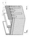
- a plurality of transistors 184may be formed on the substrate 110 .
- Each of the fin rows 170may include a plurality of transistors 184 .
- the transistors 184 on a given fin row 170may be isolated from one another by the dielectric 146 .
- the transistors 184 in adjacent fin rows 170may be isolated from one another by the dielectric 180 .
- Each of the transistors 184may include one or both of the gates 176 and 178 disposed on either side of the fin rows 170 .
- the illustrated transistors 184may be referred to as multi-gate transistors or dual-gate transistors. Other embodiments may include transistors with more than two gates or fewer than two gates.
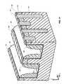
- FIG. 20illustrates the semiconductive portion of an example of a single transistor 184 .
- the transistor 184includes two legs 186 and 188 separated by a notch 189 (corresponding to trench 152 in FIG. 11 ).
- the distal portion of each of the legs 186 and 188may be formed by the upper doped region 112
- the lower portion of the legs 186 and 188may be formed by the lower doped region 114 .
- the transistor 184may generally define a fin with opposite faces 190 and 192 .
- the transistor 184may establish a conductive channel 194 extending between the legs 186 and 188 .
- This channel 194may be formed in response to electric fields emanating from the gates 176 and 178 ( FIG. 19 ). Both of the gates 176 and 178 may be held at generally the same voltage, or they may be controlled independently.
- the channel 194may extend between the upper doped region 112 of the leg 186 and the upper doped region 112 of the leg 188 , wrapping around the notch 189 .
- the channel 194may include a generally horizontal component under the notch 189 and generally vertical components along each of the legs 186 and 188 .
- the channel 194may be formed adjacent both of the faces 190 and 192 of the transistor 184 or one of the faces 190 or 192 .
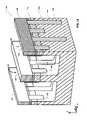
- FIGS. 21-52illustrate an example of a process for forming both connections to the transistors 184 and gates in a periphery area.
- the above-described processmay produce an array 196 and a periphery 198 on the substrate 110 .
- the array 196may include a plurality of the previously described transistors 184 arranged in a pattern, e.g., a rectangular or hexagon lattice.
- the periphery 198may generally surround the array 196 or be disposed near a portion of the array 196 , e.g., near one or more sides of the array 196 .
- FIG. 21illustrate an example of a process for forming both connections to the transistors 184 and gates in a periphery area.
- the above-described processmay produce an array 196 and a periphery 198 on the substrate 110 .
- the array 196may include a plurality of the previously described transistors 184 arranged in a pattern, e.g., a
- the periphery 198may include precursor structures for a variety of devices, such as sense amplifiers, address decoders, and drivers.
- the periphery 198may be doped differently from the array 196 .
- the periphery 198may be masked when the upper doped region 112 is formed, and separate doping steps may dope portions of the periphery 198 .
- the periphery 198may include isolation trenches 199 that may isolate subsequently-formed transistors in the periphery 198 .
- the isolation trenches 199may be patterned, etched, and filled generally simultaneously with the column isolation trenches 142 , or they may be formed partially or substantially entirely separately.
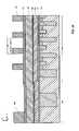
- a buffer material 200 and a stop material 202may be formed, as illustrated by FIG. 22 .
- the buffer material 200may be an oxide, e.g., an oxide formed with TEOS CVD, and the stop material 202 may be a nitride formed with CVD or other appropriate processes.
- the buffer material 200may have a thickness less than about 200 ⁇ , e.g., a thickness equal to or less than about 50 ⁇ , and the stop material 202 may have a thickness less than about 500 ⁇ , e.g., a thickness equal to or less than about 300 ⁇ .
- a mask 204may be formed on the stop material 202 , as illustrated by FIG. 23 .
- the mask 204may cover the array 196 and leave a portion or substantially all of the periphery 198 exposed.
- the mask 204may be a soft mask or a hard mask formed with photolithography or other patterning techniques.
- the mask 204may be formed with photolithography equipment that is older or less capable than the photolithography equipment used to form a certain other features on the substrate 110 , such as at the column mask 126 ( FIG. 3 ) or the row mask 160 ( FIG. 14 ).
- the mask 204may be formed with an I-line photolithography tool (e.g., a photolithography tool having a light-source with a wavelength generally equal to or greater than 365 nm) or a G-line photolithography tool (e.g., a photolithography tool having a light source with a wavelength equal to or greater than 436 nm).
- the masks 126 and 160may be formed with a deep-UV photolithography tool (e.g., a photolithography tool having a light source with a wavelength generally equal to or less than 300 nm, a 248 nm, 193 nm, or 157 nm).
- the present techniqueis not limited to masks formed with these photolithography tools.
- the masks 126 and 160may be formed with a deep-UV photolithography tool, and the mask 204 may be formed with a more advanced form of this tool, such as a deep-UV photolithography tool configured for immersion lithography or double patterning.
- the exposed portion of the stop material 202 and the mask 204may be removed, as illustrated by FIG. 24 .
- the stop material 202may be removed with a wet etch or a dry etch that is selective to the stop material 202 .
- the stop material 202may remain over the array 196 , and the buffer material 200 may be exposed in the periphery 198 .
- the lower conductive material 206may be made of or include a conductive material, e.g., p+ doped polysilicon.
- the lower conductive material 206may have a thickness less than about 1200 ⁇ , e.g., a thickness equal to or less than about 700 ⁇ . Making the lower conductive material 206 from doped polysilicon may facilitate certain subsequent higher temperature processing, as polysilicon is believed to be more resistant to oxidation than some other conductors.
- the lower conductive material 206may include a metal, such as tungsten, and liners such as titanium nitride and titanium.
- the upper stop material 208may include or be made of a material selected to function as an etch stop. That is, the choice of the upper stop material 208 may be made in view of the etch used to etch the sacrificial material 210 .
- the upper stop material 208may be selected to be relatively resistant to this etch, slowing this etch and increasing the margin for over etching the sacrificial material 210 .
- the upper stop material 208may be an oxide or a nitride, and the upper stop material 208 may have a thickness less than about 200 ⁇ , e.g., a thickness equal to or less than about 100 ⁇ .
- the upper stop material 208may facilitate relatively tight control of the vertical dimension of etches through the film stack illustrated by FIG. 25 .
- the sacrificial material 210may be a material selected to etch relatively anisotropically, e.g., a material that tends to form relatively vertical sidewalls when etched.
- the sacrificial material 210may include doped or undoped polysilicon.
- the sacrificial material 210may have a thickness less than about 2500 ⁇ , e.g., a thickness equal to or less than about 1500 ⁇ . Making the sacrificial material 210 from polysilicon is believed to facilitate formation of sidewalls that are relatively vertical as compared to sidewalls produces by etches through other materials, such as oxide. Relatively vertical sidewalls are believed to facilitate more precise control of device dimensions.
- film thickness variationsmay affect the width of the bottom of trenches.
- relatively vertical sidewallsmay cause the film thickness to have less of an effect on the width of features near the bottom of the film being etched.
- sidewall spacersmay be formed on the relatively vertical sidewalls with more margin for over etch in horizontal areas, thereby reducing the likelihood of undesirable stringers between sidewalls spacers.
- the sacrificial material 210may facilitate relatively precise control of the horizontal dimensions of the structures formed by etches through this film stack.
- the implant barrier 212may include an amorphous material, such as an oxide or amorphous carbon, and it may have a thickness equal to or less than about 1000 ⁇ , e.g., a thickness equal to or less than about 500 ⁇ .
- the implant barriermay impede implanted ions from penetrating the sacrificial material 210 , as some crystal grains in the sacrificial material 210 may align with the implant beam and may be relatively permeable to the implanted ions. It should be noted, though, that not all embodiments offer all of the advantages of the film stack illustrated by FIG. 25 , and some embodiments offer only some of its advantages or other advantages.
- the mask 214may be a soft mask or a hard mask formed with photolithography or other patterning techniques known in the art.
- the mask 214may include a pattern of lines that define a mask width 216 , an exposed width 218 , and a pitch 220 in the array 196 .
- the pitch 220may be generally equal to (or an integer multiple of) the pitch 132 of the column mask 126 described above with reference to FIG. 3 .
- the lines of the mask 214 that define the masked width 216may generally extend in the Y-direction and may generally be aligned with one of the legs 186 or 188 of each of the transistors 184 ( FIG. 20 ).
- the masked width 216may be less than the exposed width 218 and may be less than or generally equal to F, 3 ⁇ 4 F, or 1 ⁇ 2 F.
- the mask 214may also define a masked region 222 in the periphery 198 .
- the mask 214may be formed by more advanced photolithography equipment relative to the photolithography equipment used to form other structures on the substrate 110 .
- the mask 214may be formed by the photolithography equipment used to form the masks 126 ( FIG. 3) and 160 ( FIG. 14 ), equipment which may have a minimum feature size (F) that is smaller than the minimum feature size of the photolithography equipment used to form the mask 204 ( FIG. 23 ).
- Fmay be smaller than or generally equal to about 120 ⁇ , 100 ⁇ , 80 ⁇ , or 50 ⁇ .
- the masks 214 , 126 , and 160may be formed with deep-UV photolithograph equipment, and the mask 204 may be formed with I-line photolithography equipment.
- the masked region 222may define a gate of a subsequently formed transistor in the periphery 198 .
- the mask 214may serve dual purposes: defining the gates in the periphery 198 and, as explained below, data lines in the array 196 . Because the mask 214 may serve these dual purposes, the throughput of the more advanced photolithography equipment is economized, as dimensions of several structures may be defined simultaneously. It should be noted, though, that not all embodiments offer this advantage, and some embodiments offer other advantages.
- the substrate 110may be etched, as illustrated by FIG. 27 .
- the etchmay be generally anisotropic, and it may stop on or in the stop material 202 or the buffer material 200 .
- the etchmay form generally linear recesses 224 in the array 196 and the recess 226 in the periphery 198 .
- the recesses 224may be disposed over one of the legs 186 or 188 of the transistors 184 ( FIG. 20 ).
- the etchmay be performed in two or more stages. For example, the implant barrier 212 and the sacrificial material 210 may be etched first, using the upper stop material 208 as an etch stop.
- the portion of the etch that consumes the sacrificial material 210may be generally selective to polysilicon and selective against oxide.
- Using the upper stop material 208 as an etch stopis believed to form a relatively uniform etch front near this layer and produce relatively uniform vertical dimensions within the linear recesses 224 and the recess 226 .
- the upper stop material 208 and the lower conductive material 206may be etched, stopping on or in the stop material 202 or the buffer material 200 .
- forming the sacrificial material 210 and the lower conductive material 206 from polysiliconis believed to facilitate formation of the recesses 224 and 226 with relatively vertical sidewalls.
- the etch illustrated by FIG. 27may define a gate 227 in the periphery 198 .
- the gate 227may be made from the lower conductive material 206 , and it may be generally free of metal.
- the substrate 110may be annealed in a furnace, e.g., at a temperature greater than 400 degrees C., e.g., greater than or equal to 800 about degrees C.
- spacer materials 228 and 230may be formed, as illustrated by FIG. 28 .
- the spacer material 228may be a nitride deposited with CVD, and it may have a thickness less than about 300 ⁇ , e.g., a thickness equal to or less than about 100 ⁇ .
- the spacer material 230may be an oxide deposited with CVD, and it may have a thickness less than about 400 ⁇ , e.g., less than or equal to about 200 ⁇ .
- the spacer material 230may substantially fill the recesses 224 ( FIG. 27 ) in the array 196 .
- the spacer materials 228 and 230may form spacers (identified with the same reference numbers as the material from which they are formed), as illustrated by FIG. 29 .
- the spacers 228 and 230may be formed by generally anisotropically etching the substrate 110 . After forming the spacers 228 and 230 , a portion of the spacer material 230 may cover all or a portion of the spacer material 228 within the recesses 224 in the array 196 . The spacer etch may expose the top of the implant barrier 212 .
- the spacer material 230may be removed, as illustrated by FIG. 30 .
- the spacer material 230may be removed with a wet or dry etch that is selective to the spacer material 230 .
- a portion of the spacer material 228may remain along the bottom of the recesses 224 in the array, while a substantial portion of the periphery 198 may be not covered by the spacer material 228 .
- the spacer material 228may be patterned differently in the array 196 and the periphery 198 without using an additional photomask.
- a liner 232may be formed, as illustrated by FIG. 31 .
- the liner 232may be a nitride deposited with CVD or other appropriate processes.
- the liner 232may have a thickness less than about 300 ⁇ , e.g., a thickness equal to or less than about 150 ⁇ .
- a dielectric 234may be formed, as illustrated by FIG. 32 .
- the dielectric 234may be an oxide or other appropriate material deposited with CVD or it may be a spun-on dielectric, for example.
- the dielectric 234may be densified by heating the substrate 110 to drive volatile compounds from the dielectric 234 .
- the dielectric 234may be deposited to a thickness selected to generally planarize the substrate 110 , e.g., a thickness at least greater than the depth of the recesses 224 ( FIG. 31 ).
- the substrate 110may be planarized, as illustrated by FIG. 33 .
- Planarizingmay include polishing the substrate 110 with CMP or etching the substrate 110 with an etch that is generally nonselective to the exposed materials on the substrate 110 .
- Planarizationmay stop on or in the implant barrier 212 or on or in the upper conductor 210 , for example. In some embodiments, planarization may stop in the implant barrier 212 , and the exposed portion of the implant barrier 212 may be removed with a wet or dry etch.
- the upper conductor 210 and the upper stop material 208may be removed, as illustrated by FIG. 34 .
- the upper conductor 210may be removed with an etch, e.g. a wet etch, that is selective to the upper stop material 208 , and the upper stop material 208 may be removed with a different etch that is selective to the lower conductor 206 .
- etche.g. a wet etch
- the upper stop material 208may be removed with a different etch that is selective to the lower conductor 206 .
- One or both of these etchesmay remove a portion of the dielectric 234 as well.
- a mask 236may be formed on the substrate 110 , as illustrated by FIG. 35 .
- the mask 236may expose the array 196 and cover a portion or substantially all of the periphery 198 .
- the mask 236may be a hard mask or a soft mask formed with photolithography or other patterning techniques.
- the mask 236may be formed with photolithography equipment that is older or less capable than the photolithography equipment that was used to form certain other features on the substrate 110 , such as at the mask 214 .
- the mask 236may be formed with an I-line photolithography tool (e.g., a photolithography tool having a light-source with a wavelength generally equal to or greater than 365 nm) or a G-line photolithography tool (e.g., a photolithography tool having a light source with a wavelength equal to or greater than 436 nm), and the mask 214 ( FIG. 26 ) may be formed with a deep-UV photolithography tool (e.g., a photolithography tool having a light source with a wavelength generally equal to or less than 300 nm, a 248 nm, 193 nm, or 157 nm).
- I-line photolithography toole.g., a photolithography tool having a light-source with a wavelength generally equal to or greater than 365 nm
- a G-line photolithography toole.g., a photolithography tool having a light source with a wavelength equal to or greater than 436 nm
- the present techniqueis not limited to the present generation of photolithography tools.
- the mask 236may be formed with a deep-UV photolithography system, and the mask 214 may be formed with the more advanced system, e.g., a system with a smaller minimum feature size (F), such as a system configured for double-patterning, immersion lithography, or a smaller-wavelength light source.
- Fminimum feature size
- the portion of the lower conductor 206 that is not covered by the mask 236may be removed, as illustrated by FIG. 36 .
- This portion of the lower conductor 206may be removed with a dry or wet etch that is selective to the lower conductor 206 .
- the etchmay stop on or in the stop material 202 .
- the mask 236may be removed, and a liner material 238 may be formed on the substrate 110 , as illustrated by FIG. 37 .
- the mask 236like many of the other masks described herein, may be removed with an etch that is selective to the mask 236 or by combusting the mask 236 with oxygen in a furnace, for example.
- the liner material 238may be a nitride, an oxide, or other appropriate material, and it may be formed with CVD or other processes.
- the liner material 238may have a thickness less than about 500 ⁇ , e.g., a thickness equal to or less than about 300 ⁇ .
- the portion of the liner material 238 that is disposed on generally horizontal surfacesmay be removed to form spacers (identified with the same reference number 238 as the material from which they are formed), as illustrated by FIG. 38 .
- the liner material 238may be etched with a generally anisotropic dry etch that is selective to the liner material 238 , e.g., a dry etch that is selective to nitride.
- the resulting spacer formed by the liner material 238may narrow the recesses 242 to a width that is less than or generally equal to F, 3 ⁇ 4 F, or 1 ⁇ 2 F.
- Each recess 242may be a generally linear recess extending in the Y-direction and exposing the upper doped region 112 of one of the legs 186 or 188 ( FIG. 20 ) of the transistors 184 ( FIG. 20 ).
- the exposed portion of the upper doped region 112may be implanted, e.g., with phosphorus or other dopants, to reduce contact resistance with subsequently formed conductors.
- the recess 240may extend to the lower conductive material 206 in the periphery 198 .
- the recesses 240 and 242may extend to different structures 206 and 188 , the dimensions and position of the recesses 242 and 240 may be generally defined by a single mask 214 .
- the other masks 204 and 236 formed by less expensive lithography equipmentmay determine which structures defined by the mask 214 connect to the upper doped region 112 or the lower conductive material 206 , allowing the mask 214 to serve two purposes.
- a conductive material 244may be formed on the substrate 110 , as illustrated by FIG. 39 .
- the conductive material 244may be doped polysilicon or a metal, such as titanium, or other appropriate materials.
- the conductive material 244includes a titanium nitride liner (not shown) and a titanium liner deposited with collimated physical-vapor deposition.
- the conductive material 244may also include tungsten deposited on the titanium and titanium nitride liners. The tungsten may be less than about 400 ⁇ thick, e.g., less than or equal to about 200 ⁇ .
- Planarizingmay include polishing the substrate with CMP or etching the substrate 110 with an etch-back process (e.g., by forming a sacrificial planarizing material, such as a spun on glass or resist, on the substrate 110 and etching the sacrificial material and the conductive material 244 ). Planarization may stop on or in the dielectric 234 , forming a conductive plate 246 and data lines 248 that may be isolated from one another. The data lines 248 may extend in the Y-direction and connect to one of the legs 186 or 188 of a plurality of transistors 184 ( FIG. 20 ).
- each data line 248may connect to one leg 188 or 186 of one transistor 184 in each fin row 170 ( FIG. 19 ).
- the data lines 248may be isolated from one another by the dielectric 234 , the liner material 238 , the liner 232 , the spacer material 228 , the remaining buffer material 200 , and the remaining stop material 202 .
- the data lines 248may not extend generally straight in the Y-direction, e.g., they may undulate, vary in width, or be segmented.
- the dielectric material 250may be an oxide or other appropriate material deposited with CVD or other processes, such as a spun-on-dielectric process.
- the dielectric 250may have a thickness less than about 2000 ⁇ , e.g., a thickness equal to or less than about 1000 ⁇ or about 500 ⁇ .
- the stop material 252may be a nitride or other appropriate material selected to function as a stop layer for subsequent etches.
- the stop material 252may have a thickness less than about 2500 ⁇ , e.g., a thickness equal to or less than about 1500 ⁇ or about 1000 ⁇ .
- the sacrificial material 254may include amorphous carbon deposited with CVD, PVD, or other appropriate processes, and it may have a thickness less than or equal to about 4000 ⁇ .
- a mask 256may be formed on the sacrificial material 254 , as illustrated by FIG. 42 .
- the mask 256may generally cover the periphery 198 and define a plurality of openings 258 over the array 196 .
- the openings 258may have a generally right-circular-cylindrical shape, a generally right-elliptical-cylindrical shape, or other shape.
- the openings 258may have a diameter 260 that is generally equal to or less than F, and the openings 258 may be generally centered over one of the legs 186 or 188 of each of the transistors 184 ( FIG. 20 ).
- the mask 256may be a hard mask or a soft mask formed with photolithography or other patterning techniques.
- the portions of the conductive material 254 and the stop material 252 disposed under the openings 258may be removed to form recesses 259 , as illustrated by FIG. 43 .
- These materials 252 and 254may be removed with a wet etch or a dry etch that is generally anisotropic. The etch may stop on or in the dielectric material 250 .
- the mask 256may be removed, and a spacer 262 may be formed in the recesses 259 , as illustrated by FIG. 44 .
- the spacer 262may be formed by depositing a layer of spacer material and then generally anisotropically etching the spacer material to remove the spacer material from generally horizontal surfaces, leaving the spacers 262 in the recesses 259 .
- the spacers 262may be made of a conductive material, such as doped polysilicon or a metal, for example, or a non-conductive material.
- the spacer materialmay be deposited with a thickness less than about 800 ⁇ , e.g., a thickness equal to or less than about 400 ⁇ .
- the spacer 262may narrow the diameter of the openings 258 to a narrower diameter 264 that may be generally equal to or less than F, 3 ⁇ 4 F, or 1 ⁇ 2 F.
- the substrate 110may be etched, as illustrated by FIG. 45 .
- the substrate 110may be etched with a generally anisotropic dry etch.
- the sacrificial material 254 and the spacers 262may mask portions of the substrate 110 as the narrowed recesses 259 are extended into the substrate 110 to the buffer material 200 .
- the substrate 110may be etched to further remove the portion of the buffer material 200 disposed at the bottom of the recesses 259 , as illustrated by FIG. 46 .
- the buffer material 200may be removed with a hydrofluoric acid clean or other wet or dry etch.
- the etchmay attack portions of the side wall of the recesses 259 , such as the dielectric 250 and the dielectric 234 , and widen portions of the recesses 259 .
- the etchmay expose the surface of the upper doped region 112 ( FIG. 20 ) of one of the legs 186 or 188 of each of the transistors 184 ( FIG. 20 ).
- a conductive material 266may then be formed on the substrate 110 , as illustrated by FIG. 47 .
- the conductive material 266may be doped polysilicon (e.g., n+ doped polysilicon), a metal, or other appropriate materials, and it may have a thickness less than 700 ⁇ , e.g. a thickness less than or generally equal to 400 ⁇ .
- the conductive material 266may extend to the bottom of the recesses 259 ( FIG. 46 ).
- the conductive material 266may be generally free of metal, and the area where the conductive material 226 meets the upper doped region 112 may be generally free of silicides. Keeping this area generally free of silicides is believed to reduce current leakage. It should be noted, though, that not all embodiments offer this advantage, and some embodiments offer other advantages.
- Planarizingmay include polishing the substrate 110 with CMP or etching the substrate with an etch-back process. Planarization may stop on or in the stop material 252 , leaving a portion of the spacer material 262 and the conductive material 266 exposed.
- the spacer material 262 and the conductive material 266 togethermay form a contact 268 .
- the contacts 268may extend generally along the z-axis to one of the two legs 186 or 188 of each of the transistors 184 in the array 196 . In other embodiments, the contacts 268 may extend to transistors with other structures, e.g., a source or drain of a CMOS transistor with a generally horizontal channel between its source and drain.
- the contacts 268may be generally cylindrical structures with a generally horizontal flange formed by the spacer material 262 and having a diameter 270 . In some embodiments, the diameter 270 may be generally equal to or less than F.
- the diameter 270 and a diameter 271 of the lower portion of the contacts 268may be generally defined by a single photolithography step, and the difference between these dimensions may be generally defined by the thickness of the spacer 262 . Forming both of these dimensions 270 and 271 with a single photolithography step is believed to economize capacity of photolithography equipment. It should be noted, though, that not all embodiments offer this advantage, and some embodiments offer other advantages.
- the contacts 268generally have a T-shape.
- the spacer material 262may enlarge the target for subsequently-formed data elements, e.g., capacitor plates, ovonic devices, or imaging devices, thereby potentially increasing the alignment margin for these structures.
- the spacers 268may be generally electrically isolated from other spacers 268 on the same fin row 170 ( FIG. 19 ) and from spacers 268 on other fin rows 170 .
- a dielectric material 272may be formed, and a mask 274 may be formed on the dielectric material 272 , as illustrated by FIG. 49 .
- the dielectric material 272may be an oxide, such as an oxide deposited with CVD.
- the dielectric material 272may cover the contacts 268 .
- the dielectric material 272may have a thickness less than about 2000 ⁇ , e.g., a thickness equal to or less than about 500 ⁇ .
- the mask 274may be a soft mask or a hard mask formed with photolithography or other lithography processes.
- the mask 274may include exposed regions 276 and 278 in the periphery 198 , and it may generally mask the array 196 .
- the areas under the exposed regions 276 and 278may be etched, as illustrated by FIG. 50 .
- the etchmay be a generally anisotropic dry etch, and the etch may be generally selective against the conductive plate 246 .
- the etchmay produce an opening 280 that extends to the conductive plate 246 and an opening 282 that extends further into or to the lower doped region 214 or other portion of the substrate.
- a conductive material 284may include liners, such as titanium and titanium nitride liners (not shown) deposited with physical-vapor deposition (PVD), and tungsten or other conductive materials deposited with, for example, PVD or other processes.
- the hard-mask material 286may include carbon or other materials deposited with CVD or other processes.
- the mask 288may be formed with photolithography, and it 288 may generally leave the array 196 and portions of the periphery 198 exposed.
- the substrate 110may be etched to form contacts 290 and 292 , as illustrated by FIG. 52 .
- the substrate 110may be etched with an etch that is generally anisotropic, such as a dry etch. The etch may stop on or in the dielectric 272 .
- the contacts 292may connect to the gates 176 and 178 on either side of a fin row 170 ( FIG. 19 ).
- the contact 292may be referred to as a “word line contact.“The contact 292 may straddle one fin row 170 , and different contacts 292 may contact to other gates 176 and 178 on other fin rows 170 ( FIG. 19 ).
- the contact 290may connect to a gate stack 294 formed from the conductive plate 246 and the lower conductive material 206 .
Landscapes
- Engineering & Computer Science (AREA)
- Physics & Mathematics (AREA)
- Condensed Matter Physics & Semiconductors (AREA)
- General Physics & Mathematics (AREA)
- Manufacturing & Machinery (AREA)
- Computer Hardware Design (AREA)
- Microelectronics & Electronic Packaging (AREA)
- Power Engineering (AREA)
- Semiconductor Memories (AREA)
- Internal Circuitry In Semiconductor Integrated Circuit Devices (AREA)
- Element Separation (AREA)
Abstract
Description
- 1. Field of Invention
- Embodiments of the invention relate generally to electronic devices and, more specifically, in certain embodiments, to methods of forming connections to data cells.
- 2. Description of Related Art
- Many types of electronic devices have data cells. Typically, the data cells each include a data element (e.g., a memory element, an imaging element, or other device configured to output data, such as various kinds of sensors) and, in some instances, an access device, such as a transistor or diode. Generally, the access device controls access to the data element, and the data element outputs signals indicative of stored or sensed data.
- Often the data elements are arranged in an array, e.g., generally in rows and columns. Data cells within the array are accessed, e.g., written to or read from, through circuitry near the periphery of the array. For instance, sense amplifiers or other sensing circuitry are often positioned adjacent arrays of data cells for reading data. Similarly, address decoders, e.g., row and column address decoders, are often disposed adjacent the array for addressing particular data cells or groups of data cells.
- Devices in the array often are structured differently from structures in the periphery. Array transistors may be formed from materials that are different from the materials used to form transistors in the periphery, and the dimensions, e.g., thickness, of materials in these devices may be different. In some devices, differences between the array and periphery are accommodated with multiple lithography steps. For instance, a first photolithography tool may pattern a first material in the array, and a second, different photolithography tool, may pattern a second, different material in the periphery. In this way, different design tradeoffs, e.g., size versus signal quality, may be made between the array devices and the periphery devices.
- These differences, however, can increase the cost of electronic devices. Each lithography step adds costs, and certain lithography steps are particularly expensive. Typically, manufacturing lines use several different generations of lithography equipment, ranging from more advanced, newer equipment to less capable, older equipment. The newer equipment is typically much more expensive, so designers strive to reduce the number of manufacturing steps that use the newer lithography equipment. Patterning array and periphery devices, however, is often done with separate lithography steps on the newer equipment, adding to the cost of electronic devices.
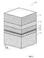
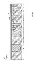
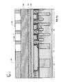
FIGS. 1-20 illustrate an example of a process for forming an array of transistors; andFIGS. 21-52 illustrate an example of a process for forming connections to the array ofFIGS. 1-20 and for forming a gate of periphery transistors.FIG. 1 illustrates a first step in an embodiment of a process for forming an array of transistors. The process may begin with providing asubstrate 110. Thesubstrate 110 may include semiconductive materials such as single-crystal or poly-crystalline silicon, gallium arsenide, indium phosphide, or other materials with semiconductor properties. Alternately, or additionally, thesubstrate 110 may include a non-semiconductor body on which an electronic device may be constructed, e.g., a body such as a plastic or ceramic work surface. The term “substrate” encompasses these structures in a variety of stages of manufacture, including an unprocessed whole wafer, a partially-processed whole wafer, a fully-processed whole wafer, a portion of a diced wafer, or a portion of a diced wafer in a packaged electronic device.- The
substrate 110 may include an upperdoped region 112 and a lowerdoped region 114. The depth of the upperdoped region 112 may be generally uniform over a substantial area of thesubstrate 110, and the upperdoped region 112 may be doped differently from the lowerdoped region 114. For example, the upper-dopedregion 112 may include an n+ material and the lower-dopedregion 114 may include a p− material or vise versa. - Next, several films may be formed on the
substrate 110, as illustrated byFIG. 2 . Apad oxide 116 may be formed on the upper dopedregion 112. Thepad oxide 116 may have a thickness less than 300 Å, e.g., less than or equal to about 80 Å may be useful. Thepad oxide 116 may be formed with a variety of techniques. For instance, it may be grown by exposing thesubstrate 110 to oxygen, e.g., in a diffusion furnace, or it may be deposited with atomic-layer deposition (ALD), chemical-vapor deposition (CVD), or other processes. A stop body (e.g., a layer)118 may be formed on thepad oxide 116 with, for example, CVD. Thestop body 118 may include a nitride, such as silicon nitride, and it may have a thickness less than 300 Å, e.g., about 95 Å may be useful, but like the other structures described herein, thestop body 118 is not limited to these dimensions or materials. Asacrificial body 120 may be formed on thestop body 118. Thesacrificial body 120 may be made of polysilicon and it may have a thickness between about 500 Å and about 2,000 Å, e.g., about 1000 Å may be useful. Thesacrificial body 120 may be formed with CVD or other appropriate processes. Alower masking body 122 may be formed on thesacrificial body 120. Thelower masking body 122 may be made of an oxide and it may have a thickness between about 500 Å and about 2,000 Å, e.g., about 1000 Å may be useful. Thelower masking body 122 may be formed with CVD, a spun-on-dielectric process, or other processes. Finally, anupper masking body 124 may be formed on thelower masking body 122. Theupper masking body 124 may be made of carbon or other materials formed with CVD or other processes, and it may have a thickness between about 1000 Å and abut 3000 Å, e.g., about 2000 Å may be useful. - Next, a
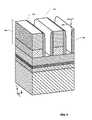
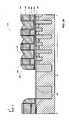
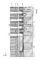
column mask 126 may be formed, as illustrated byFIG. 3 . (The term “column” does not refer to any particular horizontal direction on thesubstrate 110 other than a direction that is different from the direction that subsequently-introduced rows extend.) Thecolumn mask 126 may include a pattern of lines that define masked regions having awidth 128 and exposed regions having awidth 130. Thewidths column mask 126 may have a pitch132 (e.g., a distance over which a pattern repeats) that is generally equal to 2 F. The lines formed by thecolumn mask 126 may be generally straight, generally parallel to each other, and may generally extend in the Y-direction. These lines may be generally continuous and generally uniform in the Y-direction. In other embodiments, though, the lines formed by thecolumn mask 126 may have other shapes, e.g., they may undulate (e.g., up and down, left and right, or both), they may vary in width in the Y-direction, or they may be formed from a plurality of shorter segments. - After forming the
column mask 126, a columnhard mask 134 may be formed, as illustrated byFIG. 4 . The columnhard mask 134 may be formed by generally-anisotropically etching (e.g., with a directional plasma etch) the portion of theupper masking body 124 and the portion of thelower masking body 122 that are disposed under the region not covered by thecolumn mask 126. In some embodiments, the etch may stop on or in thesacrificial body 120. - Next, the
column mask 126 may be removed, and thecolumn spacers 136 may be formed on the sidewalls of the columnhard mask 134, as illustrated byFIG. 5 . Thecolumn spacers 136 may be formed by depositing a generally conformal film (e.g., a film that is of generally uniform thickness on both vertical and horizontal structures) and, then, anisotropically etching that film to remove it from horizontal surfaces, leaving material disposed against generally vertical surfaces on thesubstrate 110. Thecolumn spacers 136 may be made of an oxide, and they may have awidth 138 that is less than 100 nm, e.g., less than or equal to about 36 nm. Thecolumn spacers 136 may narrow the area exposed by the columnhard mask 134 to awidth 140 that is less than or equal to F, e.g., generally equal to or less than ¾ F, ½ F, or ¼ F. - Next, as illustrated by
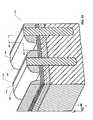
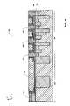
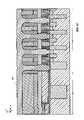
FIG. 6 ,column isolation trenches 142 may be formed. Thecolumn isolation trenches 142 may be formed by generally anisotropically etching the exposed regions between thecolumn spacers 136. Thecolumn isolation trenches 142 may have awidth 141 that corresponds to (e.g., is generally equal to or is proportional to) thewidth 140. Thecolumn isolation trenches 142 may generally extend in the Y-direction and may be generally parallel to each other and generally straight. The cross-sectional shape of thecolumn isolation trenches 142 may be generally uniform in the Y-direction. In some embodiments, thecolumn isolation trenches 142 may have adepth 144 that is between about 500 Å and about 5000 Å, e.g., about 2500 Å. - After forming the
column isolation trenches 142, they may be filled partially or entirely with a dielectric146, as illustrated byFIG. 7 . The dielectric146 may be made of a variety of materials, such as an oxide, and it may be lined with a variety of liner films (not shown), such as an oxide liner and a nitride liner. The dielectric146 may be formed with a variety of processes, such as a high-density plasma CVD process. In some embodiments, prior to forming the dielectric146, the bottom of thecolumn isolation trenches 142 may be implanted or diffused with a dopant (not shown) selected to further electrically isolate structures on opposing sides of thecolumn isolation trenches 142. - Next, the
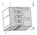
substrate 110 may be planarized, as illustrated byFIG. 8 . Planarizing thesubstrate 110 may include etching thesubstrate 110 or polishing the substrate with chemical-mechanical planarization (CMP). Planarization may include removing both theupper masking body 124 and thelower masking body 122, and planarization may stop on or in thesacrificial body 120. Additionally, an upper portion of the dielectric146 may be removed. - Next, the
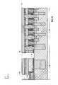
sacrificial body 120 may be partially or entirely removed, as illustrated byFIG. 9 . Removing thesacrificial body 120 may include wet etching or dry etching thesubstrate 110 with an etch that selectively etches thesacrificial body 120 without removing a substantial portion of the exposeddielectric 146, i.e., with an etch that is selective to thesacrificial body 120. An etch is said to be “selective to” a material if the etch removes that material without removing a substantial amount of other types of material exposed on the substrate. After removing thesacrificial body 120, generallyvertical projections 148 formed by the dielectric146 may extend from thesubstrate 110. - Next, a
second spacer 150 may be formed on the sidewalls of the generallyvertical projections 148 ofdielectric 146, as illustrated byFIG. 10 . As with the previously-describedcolumn spacers 136, thesecond column spacers 150 may be formed by depositing a generally conformal film on thesubstrate 110 and anisotropically etching the film until the film is generally removed from the horizontal surfaces, leaving the material on the vertical surfaces on thesubstrate 110. Thesecond column spacers 150 may be made of the same material as the dielectric146, e.g., an oxide, or they may be made of a different material. Thesecond column spacers 150 may have awidth 152 that is less than or generally equal to 100 nm, e.g., less than or generally equal to 36 nm. Thespacers 150 may define awidth 154 betweenadjacent spacers 150 that is generally less than or equal to 1 F,3/4 F, ½ F, or ¼ F. - After forming the second group of
column spaces 150, anintra-device trench 152 may be formed, as illustrated byFIG. 11 . Theintra-device trench 152 may be formed by generally anisotropically etching the exposed regions between thesecond column spacers 150. Theintra-device trenches 152 may be generally parallel to each other and thecolumn isolation trenches 142, and they may generally extend in the Y-direction. Theintra-device trenches 152 may have adepth 154 that is both less than the depth144 (FIG. 6 ) of thecolumn isolation trenches 142 and greater than the depth of the upperdoped region 112. - Next, a dielectric156 may be formed, as illustrated by
FIG. 12 . The dielectric156 may be formed with a thickness that produces anoverburden 158, increasing the likelihood that theintra-device trenches 152 are filled. For example, the dielectric156 may have a thickness less than about 800 Å, e.g., less than or equal to about 400 Å. The dielectric156 may include or be formed primarily with tetra-ethyl-ortho silane (TEOS), e.g., with TEOS CVD, or other appropriate dielectric materials. The dielectric156 may be densified after being formed by heating thesubstrate 110 to drive volatile compounds from the dielectric156. - After forming the dielectric156, the
substrate 110 may be planarized, as illustrated byFIG. 13 . Thesubstrate 110 may be planarized with CMP, an etch-back process (e.g., by depositing a sacrificial planarizing material and then etching through the sacrificial planarizing material and into underlying structures), or other appropriate processes. The stop body118 (FIG. 2 ) may function as a planarization stop, impeding removal of material from the upperdoped region 112 and thepad oxide 116. After planarization, the material from thestop body 118 remaining on thesubstrate 110 may be removed, e.g., with a wet etch that stops in thepad oxide 116 or the upperdoped region 112. - Next, a
row mask 160 may be formed, as illustrated byFIG. 14 . Therow mask 160 may be generally perpendicular to the column mask126 (FIG. 4 ). Therow mask 160 may be formed with photoresist or it may be a hard mask, for example, and it may be patterned with photolithography or other lithographic processes, e.g., nano-imprint lithography or electron-beam lithography. For example, therow mask 160 may be formed by patterning a body of amorphous carbon that is formed on thesubstrate 110. The amorphous carbon may be formed with a thickness less than about 3000 Å, e.g., a thickness less than or equal to about 2000 Å. Therow mask 160 may define masked regions having awidth 162 and exposed regions having a width164. In some embodiments, therow mask 160 may be formed with a sub-photolithographic process, e.g., a sidewall-spacer process, a resist-reflow process, or a line-width thinning process. Thewidths 162 or164 may be generally equal to or less than F, ¾ F, or ½ F. Therow mask 160 may define a repeating pattern of lines with a pitch166, or in some embodiments, the pattern may be interrupted by other structures. The masked regions of therow mask 160 may be generally straight, generally parallel to one another, and may generally extend in the X-direction. In other embodiments, the masked regions of therow mask 160 may undulate side to side or up and down, or they may be segmented. - Next,
row trenches 168 may be formed, as illustrated byFIG. 15 . Therow trenches 168 may definefin rows 170 disposed under the masked region of therow mask 160. Therow trenches 168 may be formed with a dry etch that etches the upperdoped region 112, the lower dopedregion 114, the dielectric146, and the dielectric156 at generally the same rate. Therow trenches 168 may have adepth 172 that is greater than the depth of the intra-device trenches152 (FIG. 11 ) and less than a depth of the column isolation trenches142 (FIG. 11 ). Thedepth 172 may be less than about 3000 Å, e.g., equal to or less than about 1400 Å. - A
gate dielectric 174 may be formed in therow trenches 168, as illustrated byFIG. 16 . Thegate dielectric 174 may be deposited, grown, or otherwise formed, and it may substantially or entirely cover the exposed portions of the upperdoped region 112 and the lower dopedregion 114. Thegate dielectric 174 may include a variety of dielectric materials, such as oxide (e.g., silicon dioxide), oxynitride, or high-dielectric constant materials like hafnium dioxide, zirconium dioxide, and titanium dioxide. Thegate dielectric 174 may have a thickness less than about 60 Å, e.g., a thickness equal to or less than about 40 Å. - Next,
gates fin rows 170, as illustrated byFIG. 17 . Thegates fin rows 170, or they may be electrically independent. Thegates doped region 112. Thegates substrate 110 and, then, anisotropically etching the conductive film until the conductive film is generally removed from horizontal surfaces, leaving conductive material disposed against generally vertical surfaces. For example, thegates protective body 118 may be removed with another etch that selectively removes the protective body, while leaving a substantial portion of the conductive material disposed against the sidewalls of thefin rows 170. - After forming the
gates substrate 110, as illustrated byFIG. 18 . The dielectric180 may be formed with anoverburden 182 to increase the likelihood of covering thegates substrate 110. The dielectric180 may include an oxide formed with TEOS CVD or other appropriate materials. In some embodiments, the dielectric180 is formed with a thickness of less than about 1500 Å, e.g., equal to or less than about 1000 Å. - Next, the
substrate 110 may be planarized, as illustrated byFIG. 19 . Planarization may include processing thesubstrate 110 with a CMP process, an etch-back process, or other processes that planarize. The planarization process may stop on or in the upperdoped region 112, removing theoverburden 182 of the dielectric180. - As illustrated by
FIG. 19 , a plurality oftransistors 184 may be formed on thesubstrate 110. Each of thefin rows 170 may include a plurality oftransistors 184. Thetransistors 184 on a givenfin row 170 may be isolated from one another by the dielectric146. Thetransistors 184 inadjacent fin rows 170 may be isolated from one another by the dielectric180. Each of thetransistors 184 may include one or both of thegates fin rows 170. The illustratedtransistors 184 may be referred to as multi-gate transistors or dual-gate transistors. Other embodiments may include transistors with more than two gates or fewer than two gates. FIG. 20 illustrates the semiconductive portion of an example of asingle transistor 184. Thetransistor 184 includes twolegs FIG. 11 ). The distal portion of each of thelegs doped region 112, and the lower portion of thelegs region 114. Thetransistor 184 may generally define a fin withopposite faces - In operation, the
transistor 184 may establish aconductive channel 194 extending between thelegs channel 194 may be formed in response to electric fields emanating from thegates 176 and178 (FIG. 19 ). Both of thegates channel 194 may extend between the upperdoped region 112 of theleg 186 and the upperdoped region 112 of theleg 188, wrapping around thenotch 189. Thechannel 194 may include a generally horizontal component under thenotch 189 and generally vertical components along each of thelegs gates channel 194 may be formed adjacent both of thefaces transistor 184 or one of thefaces FIGS. 21-52 illustrate an example of a process for forming both connections to thetransistors 184 and gates in a periphery area. As illustrated byFIG. 21 , the above-described process may produce anarray 196 and aperiphery 198 on thesubstrate 110. Thearray 196 may include a plurality of the previously describedtransistors 184 arranged in a pattern, e.g., a rectangular or hexagon lattice. Theperiphery 198 may generally surround thearray 196 or be disposed near a portion of thearray 196, e.g., near one or more sides of thearray 196. At the stage illustrated byFIG. 21 , theperiphery 198 may include precursor structures for a variety of devices, such as sense amplifiers, address decoders, and drivers. In some embodiments, theperiphery 198 may be doped differently from thearray 196. For example, theperiphery 198 may be masked when the upperdoped region 112 is formed, and separate doping steps may dope portions of theperiphery 198. Theperiphery 198 may includeisolation trenches 199 that may isolate subsequently-formed transistors in theperiphery 198. Theisolation trenches 199 may be patterned, etched, and filled generally simultaneously with thecolumn isolation trenches 142, or they may be formed partially or substantially entirely separately.- A
buffer material 200 and astop material 202 may be formed, as illustrated byFIG. 22 . Thebuffer material 200 may be an oxide, e.g., an oxide formed with TEOS CVD, and thestop material 202 may be a nitride formed with CVD or other appropriate processes. Thebuffer material 200 may have a thickness less than about 200 Å, e.g., a thickness equal to or less than about 50 Å, and thestop material 202 may have a thickness less than about 500 Å, e.g., a thickness equal to or less than about 300 Å. - A
mask 204 may be formed on thestop material 202, as illustrated byFIG. 23 . Themask 204 may cover thearray 196 and leave a portion or substantially all of theperiphery 198 exposed. Themask 204 may be a soft mask or a hard mask formed with photolithography or other patterning techniques. For example, themask 204 may be formed with photolithography equipment that is older or less capable than the photolithography equipment used to form a certain other features on thesubstrate 110, such as at the column mask126 (FIG. 3 ) or the row mask160 (FIG. 14 ). Themask 204 may be formed with an I-line photolithography tool (e.g., a photolithography tool having a light-source with a wavelength generally equal to or greater than 365 nm) or a G-line photolithography tool (e.g., a photolithography tool having a light source with a wavelength equal to or greater than 436 nm). In comparison, themasks masks mask 204 may be formed with a more advanced form of this tool, such as a deep-UV photolithography tool configured for immersion lithography or double patterning. - Next, the exposed portion of the
stop material 202 and themask 204 may be removed, as illustrated byFIG. 24 . Thestop material 202 may be removed with a wet etch or a dry etch that is selective to thestop material 202. Thestop material 202 may remain over thearray 196, and thebuffer material 200 may be exposed in theperiphery 198. - Next, a lower
conductive material 206, anupper stop material 208, asacrificial material 210, and animplant barrier 212 may be formed, as illustrated byFIG. 25 . The lowerconductive material 206 may be made of or include a conductive material, e.g., p+ doped polysilicon. The lowerconductive material 206 may have a thickness less than about 1200 Å, e.g., a thickness equal to or less than about 700 Å. Making the lowerconductive material 206 from doped polysilicon may facilitate certain subsequent higher temperature processing, as polysilicon is believed to be more resistant to oxidation than some other conductors. For instance, metals may oxidize at temperatures typically used to anneal thesubstrate 110 to heal etch damage to the crystal structure of thesubstrate 110. Indeed, the film stack illustrated byFIG. 25 , which as explained below, after etching, generally defines the dimensions of the gates in theperiphery 198, may be generally free of metal. In other embodiments, the lowerconductive material 206 may include a metal, such as tungsten, and liners such as titanium nitride and titanium. - The
upper stop material 208 may include or be made of a material selected to function as an etch stop. That is, the choice of theupper stop material 208 may be made in view of the etch used to etch thesacrificial material 210. Theupper stop material 208 may be selected to be relatively resistant to this etch, slowing this etch and increasing the margin for over etching thesacrificial material 210. For example, theupper stop material 208 may be an oxide or a nitride, and theupper stop material 208 may have a thickness less than about 200 Å, e.g., a thickness equal to or less than about 100 Å. Thus, theupper stop material 208 may facilitate relatively tight control of the vertical dimension of etches through the film stack illustrated byFIG. 25 . - The
sacrificial material 210 may be a material selected to etch relatively anisotropically, e.g., a material that tends to form relatively vertical sidewalls when etched. For example, thesacrificial material 210 may include doped or undoped polysilicon. Thesacrificial material 210 may have a thickness less than about 2500 Å, e.g., a thickness equal to or less than about 1500 Å. Making thesacrificial material 210 from polysilicon is believed to facilitate formation of sidewalls that are relatively vertical as compared to sidewalls produces by etches through other materials, such as oxide. Relatively vertical sidewalls are believed to facilitate more precise control of device dimensions. With highly sloped sidewalls, film thickness variations may affect the width of the bottom of trenches. In contrast, relatively vertical sidewalls may cause the film thickness to have less of an effect on the width of features near the bottom of the film being etched. Further, sidewall spacers may be formed on the relatively vertical sidewalls with more margin for over etch in horizontal areas, thereby reducing the likelihood of undesirable stringers between sidewalls spacers. Thus, thesacrificial material 210 may facilitate relatively precise control of the horizontal dimensions of the structures formed by etches through this film stack. - The
implant barrier 212 may include an amorphous material, such as an oxide or amorphous carbon, and it may have a thickness equal to or less than about 1000 Å, e.g., a thickness equal to or less than about 500 Å. The implant barrier may impede implanted ions from penetrating thesacrificial material 210, as some crystal grains in thesacrificial material 210 may align with the implant beam and may be relatively permeable to the implanted ions. It should be noted, though, that not all embodiments offer all of the advantages of the film stack illustrated byFIG. 25 , and some embodiments offer only some of its advantages or other advantages. - Next, a
mask 214 may be formed, as illustrated byFIG. 26 . Themask 214 may be a soft mask or a hard mask formed with photolithography or other patterning techniques known in the art. Themask 214 may include a pattern of lines that define amask width 216, an exposedwidth 218, and a pitch220 in thearray 196. The pitch220 may be generally equal to (or an integer multiple of) thepitch 132 of thecolumn mask 126 described above with reference toFIG. 3 . The lines of themask 214 that define themasked width 216 may generally extend in the Y-direction and may generally be aligned with one of thelegs FIG. 20 ). Themasked width 216 may be less than the exposedwidth 218 and may be less than or generally equal to F, ¾ F, or ½ F. Themask 214 may also define amasked region 222 in theperiphery 198. - The
mask 214 may be formed by more advanced photolithography equipment relative to the photolithography equipment used to form other structures on thesubstrate 110. For instance, themask 214 may be formed by the photolithography equipment used to form the masks126 (FIG. 3) and 160 (FIG. 14 ), equipment which may have a minimum feature size (F) that is smaller than the minimum feature size of the photolithography equipment used to form the mask204 (FIG. 23 ). F may be smaller than or generally equal to about 120 Å, 100 Å, 80 Å, or 50 Å. Themasks mask 204 may be formed with I-line photolithography equipment. - The
masked region 222 may define a gate of a subsequently formed transistor in theperiphery 198. Thus, in some embodiments, themask 214 may serve dual purposes: defining the gates in theperiphery 198 and, as explained below, data lines in thearray 196. Because themask 214 may serve these dual purposes, the throughput of the more advanced photolithography equipment is economized, as dimensions of several structures may be defined simultaneously. It should be noted, though, that not all embodiments offer this advantage, and some embodiments offer other advantages. - After forming the
mask 214, thesubstrate 110 may be etched, as illustrated byFIG. 27 . The etch may be generally anisotropic, and it may stop on or in thestop material 202 or thebuffer material 200. The etch may form generallylinear recesses 224 in thearray 196 and therecess 226 in theperiphery 198. Therecesses 224 may be disposed over one of thelegs FIG. 20 ). The etch may be performed in two or more stages. For example, theimplant barrier 212 and thesacrificial material 210 may be etched first, using theupper stop material 208 as an etch stop. The portion of the etch that consumes thesacrificial material 210 may be generally selective to polysilicon and selective against oxide. Using theupper stop material 208 as an etch stop is believed to form a relatively uniform etch front near this layer and produce relatively uniform vertical dimensions within thelinear recesses 224 and therecess 226. Next, theupper stop material 208 and the lowerconductive material 206 may be etched, stopping on or in thestop material 202 or thebuffer material 200. As mentioned above, forming thesacrificial material 210 and the lowerconductive material 206 from polysilicon is believed to facilitate formation of therecesses - The etch illustrated by
FIG. 27 may define agate 227 in theperiphery 198. Thegate 227 may be made from the lowerconductive material 206, and it may be generally free of metal. After this etch, thesubstrate 110 may be annealed in a furnace, e.g., at a temperature greater than 400 degrees C., e.g., greater than or equal to 800 about degrees C. - Next,
spacer materials FIG. 28 . Thespacer material 228 may be a nitride deposited with CVD, and it may have a thickness less than about 300 Å, e.g., a thickness equal to or less than about 100 Å. Thespacer material 230 may be an oxide deposited with CVD, and it may have a thickness less than about 400 Å, e.g., less than or equal to about 200 Å. Thespacer material 230 may substantially fill the recesses224 (FIG. 27 ) in thearray 196. - The
spacer materials FIG. 29 . Thespacers substrate 110. After forming thespacers spacer material 230 may cover all or a portion of thespacer material 228 within therecesses 224 in thearray 196. The spacer etch may expose the top of theimplant barrier 212. - Next, the
spacer material 230 may be removed, as illustrated byFIG. 30 . Thespacer material 230 may be removed with a wet or dry etch that is selective to thespacer material 230. A portion of thespacer material 228 may remain along the bottom of therecesses 224 in the array, while a substantial portion of theperiphery 198 may be not covered by thespacer material 228. Thus, thespacer material 228 may be patterned differently in thearray 196 and theperiphery 198 without using an additional photomask. - A
liner 232 may be formed, as illustrated byFIG. 31 . Theliner 232 may be a nitride deposited with CVD or other appropriate processes. Theliner 232 may have a thickness less than about 300 Å, e.g., a thickness equal to or less than about 150 Å. - Next, a dielectric234 may be formed, as illustrated by
FIG. 32 . The dielectric234 may be an oxide or other appropriate material deposited with CVD or it may be a spun-on dielectric, for example. The dielectric234 may be densified by heating thesubstrate 110 to drive volatile compounds from the dielectric234. The dielectric234 may be deposited to a thickness selected to generally planarize thesubstrate 110, e.g., a thickness at least greater than the depth of the recesses224 (FIG. 31 ). - The
substrate 110 may be planarized, as illustrated byFIG. 33 . Planarizing may include polishing thesubstrate 110 with CMP or etching thesubstrate 110 with an etch that is generally nonselective to the exposed materials on thesubstrate 110. Planarization may stop on or in theimplant barrier 212 or on or in theupper conductor 210, for example. In some embodiments, planarization may stop in theimplant barrier 212, and the exposed portion of theimplant barrier 212 may be removed with a wet or dry etch. - Next, the
upper conductor 210 and theupper stop material 208 may be removed, as illustrated byFIG. 34 . Theupper conductor 210 may be removed with an etch, e.g. a wet etch, that is selective to theupper stop material 208, and theupper stop material 208 may be removed with a different etch that is selective to thelower conductor 206. One or both of these etches may remove a portion of the dielectric234 as well. - A
mask 236 may be formed on thesubstrate 110, as illustrated byFIG. 35 . Themask 236 may expose thearray 196 and cover a portion or substantially all of theperiphery 198. Themask 236 may be a hard mask or a soft mask formed with photolithography or other patterning techniques. Themask 236 may be formed with photolithography equipment that is older or less capable than the photolithography equipment that was used to form certain other features on thesubstrate 110, such as at themask 214. In some embodiments, themask 236 may be formed with an I-line photolithography tool (e.g., a photolithography tool having a light-source with a wavelength generally equal to or greater than 365 nm) or a G-line photolithography tool (e.g., a photolithography tool having a light source with a wavelength equal to or greater than 436 nm), and the mask214 (FIG. 26 ) may be formed with a deep-UV photolithography tool (e.g., a photolithography tool having a light source with a wavelength generally equal to or less than 300 nm, a 248 nm, 193 nm, or 157 nm). The present technique, however, is not limited to the present generation of photolithography tools. As photolithography advances, and deep-UV tools are usurped with more capable systems, themask 236 may be formed with a deep-UV photolithography system, and themask 214 may be formed with the more advanced system, e.g., a system with a smaller minimum feature size (F), such as a system configured for double-patterning, immersion lithography, or a smaller-wavelength light source. - Next, the portion of the
lower conductor 206 that is not covered by themask 236 may be removed, as illustrated byFIG. 36 . This portion of thelower conductor 206 may be removed with a dry or wet etch that is selective to thelower conductor 206. The etch may stop on or in thestop material 202. - The
mask 236 may be removed, and aliner material 238 may be formed on thesubstrate 110, as illustrated byFIG. 37 . Themask 236, like many of the other masks described herein, may be removed with an etch that is selective to themask 236 or by combusting themask 236 with oxygen in a furnace, for example. Theliner material 238 may be a nitride, an oxide, or other appropriate material, and it may be formed with CVD or other processes. Theliner material 238 may have a thickness less than about 500 Å, e.g., a thickness equal to or less than about 300 Å. - Next, the portion of the
liner material 238 that is disposed on generally horizontal surfaces may be removed to form spacers (identified with thesame reference number 238 as the material from which they are formed), as illustrated byFIG. 38 . Theliner material 238 may be etched with a generally anisotropic dry etch that is selective to theliner material 238, e.g., a dry etch that is selective to nitride. The resulting spacer formed by theliner material 238 may narrow therecesses 242 to a width that is less than or generally equal to F, ¾ F, or ½ F. Eachrecess 242 may be a generally linear recess extending in the Y-direction and exposing the upperdoped region 112 of one of thelegs 186 or188 (FIG. 20 ) of the transistors184 (FIG. 20 ). The exposed portion of the upperdoped region 112 may be implanted, e.g., with phosphorus or other dopants, to reduce contact resistance with subsequently formed conductors. Therecess 240 may extend to the lowerconductive material 206 in theperiphery 198. Although therecesses different structures recesses single mask 214. Theother masks mask 214 connect to the upperdoped region 112 or the lowerconductive material 206, allowing themask 214 to serve two purposes. - A
conductive material 244 may be formed on thesubstrate 110, as illustrated byFIG. 39 . Theconductive material 244 may be doped polysilicon or a metal, such as titanium, or other appropriate materials. In some embodiments, theconductive material 244 includes a titanium nitride liner (not shown) and a titanium liner deposited with collimated physical-vapor deposition. Theconductive material 244 may also include tungsten deposited on the titanium and titanium nitride liners. The tungsten may be less than about 400 Å thick, e.g., less than or equal to about 200 Å. - Next, the
substrate 110 may be planarized, as illustrated byFIG. 40 . Planarizing may include polishing the substrate with CMP or etching thesubstrate 110 with an etch-back process (e.g., by forming a sacrificial planarizing material, such as a spun on glass or resist, on thesubstrate 110 and etching the sacrificial material and the conductive material244). Planarization may stop on or in the dielectric234, forming aconductive plate 246 anddata lines 248 that may be isolated from one another. The data lines248 may extend in the Y-direction and connect to one of thelegs FIG. 20 ). For instance, eachdata line 248 may connect to oneleg transistor 184 in each fin row170 (FIG. 19 ). The data lines248 may be isolated from one another by the dielectric234, theliner material 238, theliner 232, thespacer material 228, the remainingbuffer material 200, and the remainingstop material 202. In other embodiments, thedata lines 248 may not extend generally straight in the Y-direction, e.g., they may undulate, vary in width, or be segmented. - Next, a
dielectric material 250, astop material 252, and asacrificial material 254 may be formed, as illustrated byFIG. 41 . Thedielectric material 250 may be an oxide or other appropriate material deposited with CVD or other processes, such as a spun-on-dielectric process. The dielectric250 may have a thickness less than about 2000 Å, e.g., a thickness equal to or less than about 1000 Å or about 500 Å. Thestop material 252 may be a nitride or other appropriate material selected to function as a stop layer for subsequent etches. Thestop material 252 may have a thickness less than about 2500 Å, e.g., a thickness equal to or less than about 1500 Å or about 1000 Å. Thesacrificial material 254 may include amorphous carbon deposited with CVD, PVD, or other appropriate processes, and it may have a thickness less than or equal to about 4000 Å. - A
mask 256 may be formed on thesacrificial material 254, as illustrated byFIG. 42 . Themask 256 may generally cover theperiphery 198 and define a plurality ofopenings 258 over thearray 196. Theopenings 258 may have a generally right-circular-cylindrical shape, a generally right-elliptical-cylindrical shape, or other shape. Theopenings 258 may have a diameter260 that is generally equal to or less than F, and theopenings 258 may be generally centered over one of thelegs FIG. 20 ). Themask 256 may be a hard mask or a soft mask formed with photolithography or other patterning techniques. - Next, the portions of the
conductive material 254 and thestop material 252 disposed under theopenings 258 may be removed to formrecesses 259, as illustrated byFIG. 43 . Thesematerials dielectric material 250. - The
mask 256 may be removed, and aspacer 262 may be formed in therecesses 259, as illustrated byFIG. 44 . Thespacer 262 may be formed by depositing a layer of spacer material and then generally anisotropically etching the spacer material to remove the spacer material from generally horizontal surfaces, leaving thespacers 262 in therecesses 259. Thespacers 262 may be made of a conductive material, such as doped polysilicon or a metal, for example, or a non-conductive material. The spacer material may be deposited with a thickness less than about 800 Å, e.g., a thickness equal to or less than about 400 Å. Thespacer 262 may narrow the diameter of theopenings 258 to anarrower diameter 264 that may be generally equal to or less than F, ¾ F, or ½ F. - Next, the
substrate 110 may be etched, as illustrated byFIG. 45 . Thesubstrate 110 may be etched with a generally anisotropic dry etch. During the etch, thesacrificial material 254 and thespacers 262 may mask portions of thesubstrate 110 as the narrowed recesses259 are extended into thesubstrate 110 to thebuffer material 200. - The
substrate 110 may be etched to further remove the portion of thebuffer material 200 disposed at the bottom of therecesses 259, as illustrated byFIG. 46 . Thebuffer material 200 may be removed with a hydrofluoric acid clean or other wet or dry etch. The etch may attack portions of the side wall of therecesses 259, such as the dielectric250 and the dielectric234, and widen portions of therecesses 259. The etch may expose the surface of the upper doped region112 (FIG. 20 ) of one of thelegs FIG. 20 ). - A
conductive material 266 may then be formed on thesubstrate 110, as illustrated byFIG. 47 . Theconductive material 266 may be doped polysilicon (e.g., n+ doped polysilicon), a metal, or other appropriate materials, and it may have a thickness less than 700 Å, e.g. a thickness less than or generally equal to 400 Å. Theconductive material 266 may extend to the bottom of the recesses259 (FIG. 46 ). Theconductive material 266 may be generally free of metal, and the area where theconductive material 226 meets the upperdoped region 112 may be generally free of silicides. Keeping this area generally free of silicides is believed to reduce current leakage. It should be noted, though, that not all embodiments offer this advantage, and some embodiments offer other advantages. - Next, the
substrate 110 may be planarized, as illustrated byFIG. 48 . Planarizing may include polishing thesubstrate 110 with CMP or etching the substrate with an etch-back process. Planarization may stop on or in thestop material 252, leaving a portion of thespacer material 262 and theconductive material 266 exposed. - The
spacer material 262 and theconductive material 266 together may form acontact 268. Thecontacts 268 may extend generally along the z-axis to one of the twolegs transistors 184 in thearray 196. In other embodiments, thecontacts 268 may extend to transistors with other structures, e.g., a source or drain of a CMOS transistor with a generally horizontal channel between its source and drain. Thecontacts 268 may be generally cylindrical structures with a generally horizontal flange formed by thespacer material 262 and having a diameter270. In some embodiments, the diameter270 may be generally equal to or less than F. The diameter270 and a diameter271 of the lower portion of thecontacts 268 may be generally defined by a single photolithography step, and the difference between these dimensions may be generally defined by the thickness of thespacer 262. Forming both of these dimensions270 and271 with a single photolithography step is believed to economize capacity of photolithography equipment. It should be noted, though, that not all embodiments offer this advantage, and some embodiments offer other advantages. - In the cross-section of
FIG. 48 , thecontacts 268 generally have a T-shape. Thespacer material 262 may enlarge the target for subsequently-formed data elements, e.g., capacitor plates, ovonic devices, or imaging devices, thereby potentially increasing the alignment margin for these structures. Thespacers 268 may be generally electrically isolated fromother spacers 268 on the same fin row170 (FIG. 19 ) and fromspacers 268 onother fin rows 170. - Next, a
dielectric material 272 may be formed, and amask 274 may be formed on thedielectric material 272, as illustrated byFIG. 49 . Thedielectric material 272 may be an oxide, such as an oxide deposited with CVD. Thedielectric material 272 may cover thecontacts 268. Thedielectric material 272 may have a thickness less than about 2000 Å, e.g., a thickness equal to or less than about 500 Å. Themask 274 may be a soft mask or a hard mask formed with photolithography or other lithography processes. Themask 274 may include exposedregions periphery 198, and it may generally mask thearray 196. - The areas under the exposed
regions FIG. 50 . The etch may be a generally anisotropic dry etch, and the etch may be generally selective against theconductive plate 246. The etch may produce anopening 280 that extends to theconductive plate 246 and anopening 282 that extends further into or to the lower dopedregion 214 or other portion of the substrate. - Next, a
conductive material 284, a hard-mask material 286, and amask 288 may be formed, as illustrated byFIG. 51 . Theconductive material 284 may include liners, such as titanium and titanium nitride liners (not shown) deposited with physical-vapor deposition (PVD), and tungsten or other conductive materials deposited with, for example, PVD or other processes. The hard-mask material 286 may include carbon or other materials deposited with CVD or other processes. Themask 288 may be formed with photolithography, and it288 may generally leave thearray 196 and portions of theperiphery 198 exposed. - Next, the
substrate 110 may be etched to formcontacts FIG. 52 . Thesubstrate 110 may be etched with an etch that is generally anisotropic, such as a dry etch. The etch may stop on or in the dielectric272. Thecontacts 292 may connect to thegates FIG. 19 ). Thecontact 292 may be referred to as a “word line contact.“Thecontact 292 may straddle onefin row 170, anddifferent contacts 292 may contact toother gates FIG. 19 ). Thecontact 290 may connect to a gate stack294 formed from theconductive plate 246 and the lowerconductive material 206. - While the invention may be susceptible to various modifications and alternative forms, specific embodiments have been shown by way of example in the drawings and have been described in detail herein. However, it should be understood that the invention is not intended to be limited to the particular forms disclosed. Rather, the invention is to cover all modifications, equivalents, and alternatives falling within the spirit and scope of the invention as defined by the following appended claims.
Claims (25)
Priority Applications (4)
| Application Number | Priority Date | Filing Date | Title |
|---|---|---|---|
| US12/130,825US8076229B2 (en) | 2008-05-30 | 2008-05-30 | Methods of forming data cells and connections to data cells |
| PCT/US2009/042094WO2009146229A1 (en) | 2008-05-30 | 2009-04-29 | Methods of forming data cells and connections to data cells |
| TW098115745ATWI396276B (en) | 2008-05-30 | 2009-05-12 | Methods of forming data cells and connections to data cells |
| US13/323,525US8536631B2 (en) | 2008-05-30 | 2011-12-12 | Data cells and connections to data cells |
Applications Claiming Priority (1)
| Application Number | Priority Date | Filing Date | Title |
|---|---|---|---|
| US12/130,825US8076229B2 (en) | 2008-05-30 | 2008-05-30 | Methods of forming data cells and connections to data cells |
Related Child Applications (1)
| Application Number | Title | Priority Date | Filing Date |
|---|---|---|---|
| US13/323,525DivisionUS8536631B2 (en) | 2008-05-30 | 2011-12-12 | Data cells and connections to data cells |
Publications (2)
| Publication Number | Publication Date |
|---|---|
| US20090294842A1true US20090294842A1 (en) | 2009-12-03 |
| US8076229B2 US8076229B2 (en) | 2011-12-13 |
Family
ID=40834302
Family Applications (2)
| Application Number | Title | Priority Date | Filing Date |
|---|---|---|---|
| US12/130,825Active2029-09-06US8076229B2 (en) | 2008-05-30 | 2008-05-30 | Methods of forming data cells and connections to data cells |
| US13/323,525ActiveUS8536631B2 (en) | 2008-05-30 | 2011-12-12 | Data cells and connections to data cells |
Family Applications After (1)
| Application Number | Title | Priority Date | Filing Date |
|---|---|---|---|
| US13/323,525ActiveUS8536631B2 (en) | 2008-05-30 | 2011-12-12 | Data cells and connections to data cells |
Country Status (3)
| Country | Link |
|---|---|
| US (2) | US8076229B2 (en) |
| TW (1) | TWI396276B (en) |
| WO (1) | WO2009146229A1 (en) |
Cited By (19)
| Publication number | Priority date | Publication date | Assignee | Title |
|---|---|---|---|---|
| US20100233881A1 (en)* | 2009-03-16 | 2010-09-16 | Nanya Technology Corp. | Method of manufacturing supporting structures for stack capacitor in semiconductor device |
| US8149619B2 (en) | 2008-03-20 | 2012-04-03 | Micron Technology, Inc. | Memory structure having volatile and non-volatile memory portions |
| US8294511B2 (en) | 2010-11-19 | 2012-10-23 | Micron Technology, Inc. | Vertically stacked fin transistors and methods of fabricating and operating the same |
| US8293602B2 (en) | 2010-11-19 | 2012-10-23 | Micron Technology, Inc. | Method of fabricating a finFET having cross-hair cells |
| US8334196B2 (en) | 2010-11-01 | 2012-12-18 | Micron Technology, Inc. | Methods of forming conductive contacts in the fabrication of integrated circuitry |
| US8503228B2 (en) | 2008-04-03 | 2013-08-06 | Micron Technology, Inc. | Data cells with drivers and methods of making and operating the same |
| US8647981B1 (en)* | 2012-08-31 | 2014-02-11 | Micron Technology, Inc. | Methods of forming patterns, and methods of forming integrated circuitry |
| US8716094B1 (en)* | 2012-11-21 | 2014-05-06 | Global Foundries Inc. | FinFET formation using double patterning memorization |
| US20140147943A1 (en)* | 2012-11-29 | 2014-05-29 | Taiwan Semiconductor Manufacturing Company, Ltd. | Method for Determining Carrier Concentrations in Semiconductor Fins |
| US8921899B2 (en) | 2010-11-19 | 2014-12-30 | Micron Technology, Inc. | Double gated 4F2 dram CHC cell and methods of fabricating the same |
| US9449652B2 (en) | 2008-03-20 | 2016-09-20 | Micron Technology, Inc. | Systems and devices including multi-transistor cells and methods of using, making, and operating the same |
| US9553193B2 (en) | 2010-11-19 | 2017-01-24 | Micron Technology, Inc. | Double gated fin transistors and methods of fabricating and operating the same |
| US9711393B2 (en) | 2012-10-09 | 2017-07-18 | Infineon Technologies Dresden Gmbh | Silicon on nothing devices and methods of formation thereof |
| US20180182765A1 (en)* | 2016-12-27 | 2018-06-28 | Micron Technology, Inc. | Methods of Forming Memory Arrays |
| US10242907B2 (en)* | 2016-06-07 | 2019-03-26 | Imec Vzw | Method for interrupting a line in an interconnect |
| US20190189515A1 (en)* | 2017-12-15 | 2019-06-20 | Micron Technology, Inc. | Methods Of Forming A Transistor And Methods Of Forming An Array Of Memory Cells |
| US10692887B2 (en) | 2017-08-29 | 2020-06-23 | Micron Technology, Inc. | Methods used in forming an array of memory cells |
| US20220044933A1 (en)* | 2019-06-13 | 2022-02-10 | Nanya Technology Corporation | Semiconductor device with reduced critical dimensions |
| US20240411090A1 (en)* | 2012-08-31 | 2024-12-12 | Micron Technology, Inc. | Method of forming photonics structures |
Families Citing this family (3)
| Publication number | Priority date | Publication date | Assignee | Title |
|---|---|---|---|---|
| US7915659B2 (en) | 2008-03-06 | 2011-03-29 | Micron Technology, Inc. | Devices with cavity-defined gates and methods of making the same |
| US9805934B2 (en)* | 2013-11-15 | 2017-10-31 | Taiwan Semiconductor Manufacturing Co., Ltd. | Formation of contact/via hole with self-alignment |
| KR102323660B1 (en)* | 2015-10-13 | 2021-11-08 | 삼성전자주식회사 | Method for fabricating the semiconductor device |
Citations (88)
| Publication number | Priority date | Publication date | Assignee | Title |
|---|---|---|---|---|
| US33768A (en)* | 1861-11-19 | Improvement in army cooking-wagons | ||
| US33780A (en)* | 1861-11-26 | Improvement in cattle-fastenings | ||
| US43813A (en)* | 1864-08-09 | Improved process of hardening iron | ||
| US52300A (en)* | 1866-01-30 | Improvement in gas-stoves | ||
| US52317A (en)* | 1866-01-30 | Improvement in mowing-machines | ||
| US52537A (en)* | 1866-02-13 | Improvement in straw-cutters | ||
| US62354A (en)* | 1867-02-26 | moeschler | ||
| US130825A (en)* | 1872-08-27 | Improvement in balls for masts | ||
| US3885861A (en)* | 1972-10-02 | 1975-05-27 | Hughes Aircraft Co | Liquid crystal digital reticle |
| US5160987A (en)* | 1989-10-26 | 1992-11-03 | International Business Machines Corporation | Three-dimensional semiconductor structures formed from planar layers |
| US5196910A (en)* | 1987-04-24 | 1993-03-23 | Hitachi, Ltd. | Semiconductor memory device with recessed array region |
| US5661061A (en)* | 1994-03-25 | 1997-08-26 | Hitachi, Ltd. | Process for fabricating a semiconductor integrated circuit device having the multi-layered fin structure |
| US5821513A (en)* | 1996-06-26 | 1998-10-13 | Telxon Corporation | Shopping cart mounted portable data collection device with tethered dataform reader |
| US5858829A (en)* | 1998-06-29 | 1999-01-12 | Vanguard International Semiconductor Corporation | Method for fabricating dynamic random access memory (DRAM) cells with minimum active cell areas using sidewall-spacer bit lines |
| US5925918A (en)* | 1997-07-30 | 1999-07-20 | Micron, Technology, Inc. | Gate stack with improved sidewall integrity |
| US5949057A (en)* | 1996-03-29 | 1999-09-07 | Telxon Corporation | Portable data collection device with crosshair targeting illumination assembly |
| US5966600A (en)* | 1997-11-21 | 1999-10-12 | United Semiconductor Corp. | DRAM process with a multilayer stack structure |
| US6043562A (en)* | 1996-01-26 | 2000-03-28 | Micron Technology, Inc. | Digit line architecture for dynamic memory |
| US6080674A (en)* | 1998-08-31 | 2000-06-27 | United Microelectronics Corp. | Method for forming via holes |
| US6081008A (en)* | 1996-02-14 | 2000-06-27 | Lsi Logic Corporation | Composite trench-fin capacitors for DRAM |
| US6100129A (en)* | 1998-11-09 | 2000-08-08 | Worldwide Semiconductor Manufacturing Corporation | Method for making fin-trench structured DRAM capacitor |
| US6130551A (en)* | 1998-01-19 | 2000-10-10 | Vantis Corporation | Synthesis-friendly FPGA architecture with variable length and variable timing interconnect |
| US20010003034A1 (en)* | 1999-02-22 | 2001-06-07 | Toshiharu Furukawa | Fabrication of a high density long channel dram gate with or without a grooved gate |
| US6258656B1 (en)* | 1998-09-17 | 2001-07-10 | Siemens Aktiengesellschaft | Capacitor with high-ε dielectric or ferroelectric material based on the fin stack principle and production process using a negative mold |
| US6258659B1 (en)* | 2000-11-29 | 2001-07-10 | International Business Machines Corporation | Embedded vertical DRAM cells and dual workfunction logic gates |
| US6268243B1 (en)* | 1999-04-15 | 2001-07-31 | Hyundai Electronics Industries Co., Ltd. | Method for fabricating dynamic random access memory cells |
| US6282113B1 (en)* | 1999-09-29 | 2001-08-28 | International Business Machines Corporation | Four F-squared gapless dual layer bitline DRAM array architecture |
| US6316309B1 (en)* | 1998-06-09 | 2001-11-13 | Steven John Holmes | Method of forming self-isolated and self-aligned 4F-square vertical FET-trench DRAM cells |
| US6380759B1 (en)* | 1997-10-09 | 2002-04-30 | Vantis Corporation | Variable grain architecture for FPGA integrated circuits |
| US6432769B1 (en)* | 1995-10-27 | 2002-08-13 | Hitachi, Ltd. | Semiconductor integrated circuit device and process for manufacture the same |
| US6440792B1 (en)* | 1999-11-05 | 2002-08-27 | Promos Technology, Inc. | DRAM technology of storage node formation and no conduction/isolation process of bottle-shaped deep trench |
| US20020155656A1 (en)* | 2000-07-14 | 2002-10-24 | Katsuya Hayano | Manufacturing method of semiconductor integrated circuit device, and semiconductor integrated circuit device |
| US6548850B1 (en)* | 1999-09-29 | 2003-04-15 | Infineon Technologies Ag | Trench capacitor configuration and method of producing it |
| US20030168676A1 (en)* | 1996-07-10 | 2003-09-11 | Fujitsu Limited | Semiconductor device with self-aligned contact and its manufacture |
| US20030198073A1 (en)* | 1993-09-15 | 2003-10-23 | Brent Keeth | Bi-level digit line architecture for high density DRAMS |
| US20030230783A1 (en)* | 2002-06-14 | 2003-12-18 | Josef Willer | Integrated memory circuit and method of forming an integrated memory circuit |
| US6689660B1 (en)* | 1997-07-08 | 2004-02-10 | Micron Technology, Inc. | 4 F2 folded bit line DRAM cell structure having buried bit and word lines |
| US20040027848A1 (en)* | 2002-08-12 | 2004-02-12 | Micron Technology, Inc. | 6F2 architecture ROM embedded dram |
| US20040043592A1 (en)* | 2002-08-28 | 2004-03-04 | Infineon Technologies Richmond, Lp | Method of forming a gate contact in a semiconductor device |
| US20040125636A1 (en)* | 2001-03-14 | 2004-07-01 | Wlodek Kurjanowicz | Interleaved wordline architecture |
| US20040156247A1 (en)* | 2002-09-12 | 2004-08-12 | Samsung Electronics Co., Inc. | Method of fabricating non-volatile memory device |
| US20040198065A1 (en)* | 2003-04-04 | 2004-10-07 | Sung-Kwon Lee | Method for fabricating semiconductor device with fine patterns |
| US20040202027A1 (en)* | 2003-01-21 | 2004-10-14 | Maksim Kuzmenka | Buffer amplifier architecture for semiconductor memory circuits |
| US6845033B2 (en)* | 2003-03-05 | 2005-01-18 | International Business Machines Corporation | Structure and system-on-chip integration of a two-transistor and two-capacitor memory cell for trench technology |
| US20050056940A1 (en)* | 2003-09-12 | 2005-03-17 | Sandhu Gurtej S. | Masking structure having multiple layers including an amorphous carbon layer |
| US6897107B2 (en)* | 2001-04-11 | 2005-05-24 | International Business Machines Corporation | Method for forming TTO nitride liner for improved collar protection and TTO reliability |
| US6897514B2 (en)* | 2001-03-28 | 2005-05-24 | Matrix Semiconductor, Inc. | Two mask floating gate EEPROM and method of making |
| US20050133852A1 (en)* | 1996-05-24 | 2005-06-23 | Jeng-Jye Shau | High performance embedded semiconductor memory devices with multiple dimension first-level bit-lines |
| US20050151206A1 (en)* | 2003-12-30 | 2005-07-14 | Schwerin Ulrike G. | Transistor structure with a curved channel, memory cell and memory cell array for DRAMs, and methods for fabricating a DRAM |
| US20050196918A1 (en)* | 2004-02-10 | 2005-09-08 | Schwerin Ulrike G. | DRAM memory and method for fabricating a DRAM memory cell |
| US20050245024A1 (en)* | 2004-04-29 | 2005-11-03 | Von Schwerin Ulrike G | Method for production of trench DRAM cells and a trench DRAM cell array with fin field-effect transistors with a curved channel (CFET - curved fets) |
| US6967147B1 (en)* | 2000-11-16 | 2005-11-22 | Infineon Technologies Ag | Nitrogen implantation using a shadow effect to control gate oxide thickness in DRAM semiconductor |
| US20060006446A1 (en)* | 2004-06-29 | 2006-01-12 | Schwerin Ulrike G | Method for fabricating a DRAM memory cell arrangement having fin field effect transistors and DRAM memory cell |
| US6998666B2 (en)* | 2004-01-09 | 2006-02-14 | International Business Machines Corporation | Nitrided STI liner oxide for reduced corner device impact on vertical device performance |
| US20060057814A1 (en)* | 2004-09-10 | 2006-03-16 | Rolf Weis | Fabricating a memory cell arrangement |
| US20060063328A1 (en)* | 2004-09-17 | 2006-03-23 | Chindalore Gowrishankar L | Programming and erasing structure for a floating gate memory cell and method of making |
| US20060073662A1 (en)* | 2004-10-02 | 2006-04-06 | Se-Myeong Jang | Method of manufacturing multi-channel transistor device and multi-channel transistor device manufactured using the method |
| US20060076602A1 (en)* | 2004-09-10 | 2006-04-13 | Johann Harter | Dram cell pair and dram memory cell array |
| US20060131630A1 (en)* | 2004-12-20 | 2006-06-22 | Hynix Semiconductor Inc. | Method for forming storage node of capacitor in semiconductor device |
| US20060131651A1 (en)* | 1999-08-31 | 2006-06-22 | Kabushiki Kaisha Toshiba | Semiconductor substrate and its fabrication method |
| US7091543B2 (en)* | 2003-05-15 | 2006-08-15 | Taiwan Semiconductor Manufacturing Co., Ltd. | Embedded dual-port DRAM process |
| US7098105B2 (en)* | 2004-05-26 | 2006-08-29 | Micron Technology, Inc. | Methods for forming semiconductor structures |
| US7099216B2 (en)* | 2003-09-05 | 2006-08-29 | International Business Machines Corporation | Single cycle read/write/writeback pipeline, full-wordline I/O DRAM architecture with enhanced write and single ended sensing |
| US20060197086A1 (en)* | 2005-03-04 | 2006-09-07 | Samsung Electronics Co., Ltd. | Organic light emitting diode display and manufacturing method thereof |
| US20060244106A1 (en)* | 2003-03-17 | 2006-11-02 | Kabushiki Kaisha Toshiba | Fin semiconductor device and method for fabricating the same |
| US20060246607A1 (en)* | 1993-04-02 | 2006-11-02 | Micron Technology, Inc. | Method for forming a storage cell capacitor compatible with high dielectric constant materials |
| US7132333B2 (en)* | 2004-09-10 | 2006-11-07 | Infineon Technologies Ag | Transistor, memory cell array and method of manufacturing a transistor |
| US20060270151A1 (en)* | 2005-05-31 | 2006-11-30 | Nanya Technology Corporation | Method for forming a semiconductor device |
| US20060273415A1 (en)* | 2005-06-01 | 2006-12-07 | Hyun Jung Kim | Transistor for memory device and method for manufacturing the same |
| US20060281250A1 (en)* | 2004-12-15 | 2006-12-14 | Till Schloesser | 6F2 access transistor arrangement and semiconductor memory device |
| US7151023B1 (en)* | 2005-08-01 | 2006-12-19 | International Business Machines Corporation | Metal gate MOSFET by full semiconductor metal alloy conversion |
| US20070010058A1 (en)* | 2005-07-08 | 2007-01-11 | Micron Technology, Inc. | Method and apparatus for a self-aligned recessed access device (RAD) transistor gate |
| US20070023805A1 (en)* | 2005-07-26 | 2007-02-01 | Wells David H | Reverse construction memory cell |
| US7190060B1 (en)* | 2002-01-09 | 2007-03-13 | Bridge Semiconductor Corporation | Three-dimensional stacked semiconductor package device with bent and flat leads and method of making same |
| US7195995B2 (en)* | 2002-08-29 | 2007-03-27 | Micron Technology, Inc. | Method of manufacturing a multilayered doped conductor for a contact in an integrated circuit device |
| US7205606B2 (en)* | 2003-09-17 | 2007-04-17 | Micron Technology, Inc. | DRAM access transistor |
| US20070111455A1 (en)* | 2005-11-14 | 2007-05-17 | Samsung Electronics Co., Ltd. | Fabrication of local damascene finFETs using contact type nitride damascene mask |
| US20070121414A1 (en)* | 2005-09-12 | 2007-05-31 | Promos Technologies Pte.Ltd. | Shielded bitline architecture for dynamic random access memory (dram) arrays |
| US20070134878A1 (en)* | 2005-12-09 | 2007-06-14 | Intel Corporation | Non-planar microelectronic device having isolation element to mitigate fringe effects and method to fabricate same |
| US20070145450A1 (en)* | 2005-12-28 | 2007-06-28 | Fei Wang | DRAM cell design with folded digitline sense amplifier |
| US20070166933A1 (en)* | 2006-01-16 | 2007-07-19 | Samsung Electronics Co., Ltd. | Methods of Forming Field Effect Transistors and Capacitor-Free Dynamic Random Access Memory Cells |
| US20070170522A1 (en)* | 2006-01-23 | 2007-07-26 | Hynix Semiconductor Inc. | Semiconductor device and method for fabricating the same |
| US20070176222A1 (en)* | 1996-07-18 | 2007-08-02 | Fujitsu Limited | Highly integrated and reliable DRAM and its manufacture |
| US20070176253A1 (en)* | 2006-01-31 | 2007-08-02 | Peng-Fei Wang | Transistor, memory cell and method of manufacturing a transistor |
| US20070176221A1 (en)* | 1995-06-05 | 2007-08-02 | Fujitsu Limited | Semiconductor memory device and method for fabricating the same |
| US20070190736A1 (en)* | 2006-02-16 | 2007-08-16 | An-Hsiung Liu | Overlay alignment mark and alignment method for the fabrication of trench-capacitor dram devices |
| US20070262375A1 (en)* | 2006-05-12 | 2007-11-15 | Werner Juengling | Non-planar transistor and techniques for fabricating the same |
| US7345937B2 (en)* | 2005-03-07 | 2008-03-18 | Micron Technology, Inc | Open digit line array architecture for a memory array |
Family Cites Families (15)
| Publication number | Priority date | Publication date | Assignee | Title |
|---|---|---|---|---|
| US4824521A (en) | 1987-04-01 | 1989-04-25 | Fairchild Semiconductor Corporation | Planarization of metal pillars on uneven substrates |
| US5109256A (en) | 1990-08-17 | 1992-04-28 | National Semiconductor Corporation | Schottky barrier diodes and Schottky barrier diode-clamped transistors and method of fabrication |
| WO1997028532A1 (en) | 1996-02-01 | 1997-08-07 | Micron Technology, Inc. | Digit line architecture for dynamic memory |
| US6362027B1 (en)* | 1998-07-08 | 2002-03-26 | Semiconductor Energy Laboratory Co., Ltd. | Semiconductor device, active matrix substrate, method of manufacturing the semiconductor device and method of manufacturing the active matrix substrate |
| TW388125B (en) | 1998-08-19 | 2000-04-21 | Vanguard Int Semiconduct Corp | Method for fabricating dynamic random access memory (DRAM) cells with minimum active cell areas |
| TW380316B (en) | 1998-10-15 | 2000-01-21 | Worldwide Semiconductor Mfg | Manufacturing method for fin-trench-structure capacitor of DRAM |
| WO2001061738A1 (en) | 2000-02-15 | 2001-08-23 | Steag Cvd Systems Ltd. | Dram capacitor with ultra-thin nitride layer |
| US6333229B1 (en)* | 2000-03-13 | 2001-12-25 | International Business Machines Corporation | Method for manufacturing a field effect transitor (FET) having mis-aligned-gate structure |
| KR100466689B1 (en) | 2000-08-28 | 2005-01-24 | 인터내셔널 비지네스 머신즈 코포레이션 | Compact dual-port dram architecture system and method for making same |
| US6509226B1 (en) | 2000-09-27 | 2003-01-21 | International Business Machines Corporation | Process for protecting array top oxide |
| US6576944B2 (en) | 2000-12-14 | 2003-06-10 | Infineon Technologies Ag | Self-aligned nitride pattern for improved process window |
| DE10248722A1 (en) | 2002-10-18 | 2004-05-06 | Infineon Technologies Ag | Integrated circuit arrangement with capacitor and manufacturing process |
| JP2006054431A (en) | 2004-06-29 | 2006-02-23 | Infineon Technologies Ag | Transistor, memory cell array, and transistor manufacturing method |
| DE102004043856A1 (en)* | 2004-09-10 | 2006-03-30 | Infineon Technologies Ag | Method for producing a memory cell arrangement and memory cell arrangement |
| US7687395B2 (en)* | 2006-11-02 | 2010-03-30 | International Business Machines Corporation | Contact aperture and contact via with stepped sidewall and methods for fabrication thereof |
- 2008
- 2008-05-30USUS12/130,825patent/US8076229B2/enactiveActive
- 2009
- 2009-04-29WOPCT/US2009/042094patent/WO2009146229A1/enactiveApplication Filing
- 2009-05-12TWTW098115745Apatent/TWI396276B/enactive
- 2011
- 2011-12-12USUS13/323,525patent/US8536631B2/enactiveActive
Patent Citations (93)
| Publication number | Priority date | Publication date | Assignee | Title |
|---|---|---|---|---|
| US33768A (en)* | 1861-11-19 | Improvement in army cooking-wagons | ||
| US33780A (en)* | 1861-11-26 | Improvement in cattle-fastenings | ||
| US43813A (en)* | 1864-08-09 | Improved process of hardening iron | ||
| US52300A (en)* | 1866-01-30 | Improvement in gas-stoves | ||
| US52317A (en)* | 1866-01-30 | Improvement in mowing-machines | ||
| US52537A (en)* | 1866-02-13 | Improvement in straw-cutters | ||
| US62354A (en)* | 1867-02-26 | moeschler | ||
| US130825A (en)* | 1872-08-27 | Improvement in balls for masts | ||
| US3885861A (en)* | 1972-10-02 | 1975-05-27 | Hughes Aircraft Co | Liquid crystal digital reticle |
| US5196910A (en)* | 1987-04-24 | 1993-03-23 | Hitachi, Ltd. | Semiconductor memory device with recessed array region |
| US5160987A (en)* | 1989-10-26 | 1992-11-03 | International Business Machines Corporation | Three-dimensional semiconductor structures formed from planar layers |
| US20060246607A1 (en)* | 1993-04-02 | 2006-11-02 | Micron Technology, Inc. | Method for forming a storage cell capacitor compatible with high dielectric constant materials |
| US20030198073A1 (en)* | 1993-09-15 | 2003-10-23 | Brent Keeth | Bi-level digit line architecture for high density DRAMS |
| US5661061A (en)* | 1994-03-25 | 1997-08-26 | Hitachi, Ltd. | Process for fabricating a semiconductor integrated circuit device having the multi-layered fin structure |
| US20070176221A1 (en)* | 1995-06-05 | 2007-08-02 | Fujitsu Limited | Semiconductor memory device and method for fabricating the same |
| US6432769B1 (en)* | 1995-10-27 | 2002-08-13 | Hitachi, Ltd. | Semiconductor integrated circuit device and process for manufacture the same |
| US6043562A (en)* | 1996-01-26 | 2000-03-28 | Micron Technology, Inc. | Digit line architecture for dynamic memory |
| US20040062069A1 (en)* | 1996-01-26 | 2004-04-01 | Brent Keeth | Digit line architecture for dynamic memory |
| US6081008A (en)* | 1996-02-14 | 2000-06-27 | Lsi Logic Corporation | Composite trench-fin capacitors for DRAM |
| US5949057A (en)* | 1996-03-29 | 1999-09-07 | Telxon Corporation | Portable data collection device with crosshair targeting illumination assembly |
| US20050133852A1 (en)* | 1996-05-24 | 2005-06-23 | Jeng-Jye Shau | High performance embedded semiconductor memory devices with multiple dimension first-level bit-lines |
| US5821513A (en)* | 1996-06-26 | 1998-10-13 | Telxon Corporation | Shopping cart mounted portable data collection device with tethered dataform reader |
| US20030168676A1 (en)* | 1996-07-10 | 2003-09-11 | Fujitsu Limited | Semiconductor device with self-aligned contact and its manufacture |
| US20070176222A1 (en)* | 1996-07-18 | 2007-08-02 | Fujitsu Limited | Highly integrated and reliable DRAM and its manufacture |
| US6689660B1 (en)* | 1997-07-08 | 2004-02-10 | Micron Technology, Inc. | 4 F2 folded bit line DRAM cell structure having buried bit and word lines |
| US5925918A (en)* | 1997-07-30 | 1999-07-20 | Micron, Technology, Inc. | Gate stack with improved sidewall integrity |
| US6380759B1 (en)* | 1997-10-09 | 2002-04-30 | Vantis Corporation | Variable grain architecture for FPGA integrated circuits |
| US6216257B1 (en)* | 1997-10-09 | 2001-04-10 | Vantis Corporation | FPGA device and method that includes a variable grain function architecture for implementing configuration logic blocks and a complimentary variable length interconnect architecture for providing configurable routing between configuration logic blocks |
| US5966600A (en)* | 1997-11-21 | 1999-10-12 | United Semiconductor Corp. | DRAM process with a multilayer stack structure |
| US6130551A (en)* | 1998-01-19 | 2000-10-10 | Vantis Corporation | Synthesis-friendly FPGA architecture with variable length and variable timing interconnect |
| US6316309B1 (en)* | 1998-06-09 | 2001-11-13 | Steven John Holmes | Method of forming self-isolated and self-aligned 4F-square vertical FET-trench DRAM cells |
| US6008513A (en)* | 1998-06-29 | 1999-12-28 | Vanguard International Semiconductor Corporation | Dynamic random access memory (DRAM) cells with minimum active cell areas using sidewall-space bit lines |
| US5858829A (en)* | 1998-06-29 | 1999-01-12 | Vanguard International Semiconductor Corporation | Method for fabricating dynamic random access memory (DRAM) cells with minimum active cell areas using sidewall-spacer bit lines |
| US6080674A (en)* | 1998-08-31 | 2000-06-27 | United Microelectronics Corp. | Method for forming via holes |
| US6258656B1 (en)* | 1998-09-17 | 2001-07-10 | Siemens Aktiengesellschaft | Capacitor with high-ε dielectric or ferroelectric material based on the fin stack principle and production process using a negative mold |
| US6100129A (en)* | 1998-11-09 | 2000-08-08 | Worldwide Semiconductor Manufacturing Corporation | Method for making fin-trench structured DRAM capacitor |
| US20010003034A1 (en)* | 1999-02-22 | 2001-06-07 | Toshiharu Furukawa | Fabrication of a high density long channel dram gate with or without a grooved gate |
| US6268243B1 (en)* | 1999-04-15 | 2001-07-31 | Hyundai Electronics Industries Co., Ltd. | Method for fabricating dynamic random access memory cells |
| US20060131651A1 (en)* | 1999-08-31 | 2006-06-22 | Kabushiki Kaisha Toshiba | Semiconductor substrate and its fabrication method |
| US6548850B1 (en)* | 1999-09-29 | 2003-04-15 | Infineon Technologies Ag | Trench capacitor configuration and method of producing it |
| US6282113B1 (en)* | 1999-09-29 | 2001-08-28 | International Business Machines Corporation | Four F-squared gapless dual layer bitline DRAM array architecture |
| US6440792B1 (en)* | 1999-11-05 | 2002-08-27 | Promos Technology, Inc. | DRAM technology of storage node formation and no conduction/isolation process of bottle-shaped deep trench |
| US20020155656A1 (en)* | 2000-07-14 | 2002-10-24 | Katsuya Hayano | Manufacturing method of semiconductor integrated circuit device, and semiconductor integrated circuit device |
| US6967147B1 (en)* | 2000-11-16 | 2005-11-22 | Infineon Technologies Ag | Nitrogen implantation using a shadow effect to control gate oxide thickness in DRAM semiconductor |
| US6258659B1 (en)* | 2000-11-29 | 2001-07-10 | International Business Machines Corporation | Embedded vertical DRAM cells and dual workfunction logic gates |
| US20040125636A1 (en)* | 2001-03-14 | 2004-07-01 | Wlodek Kurjanowicz | Interleaved wordline architecture |
| US6897514B2 (en)* | 2001-03-28 | 2005-05-24 | Matrix Semiconductor, Inc. | Two mask floating gate EEPROM and method of making |
| US6897107B2 (en)* | 2001-04-11 | 2005-05-24 | International Business Machines Corporation | Method for forming TTO nitride liner for improved collar protection and TTO reliability |
| US7190060B1 (en)* | 2002-01-09 | 2007-03-13 | Bridge Semiconductor Corporation | Three-dimensional stacked semiconductor package device with bent and flat leads and method of making same |
| US20030230783A1 (en)* | 2002-06-14 | 2003-12-18 | Josef Willer | Integrated memory circuit and method of forming an integrated memory circuit |
| US20040027848A1 (en)* | 2002-08-12 | 2004-02-12 | Micron Technology, Inc. | 6F2 architecture ROM embedded dram |
| US20040043592A1 (en)* | 2002-08-28 | 2004-03-04 | Infineon Technologies Richmond, Lp | Method of forming a gate contact in a semiconductor device |
| US6927462B2 (en)* | 2002-08-28 | 2005-08-09 | Infineon Technologes Richmond, Lp | Method of forming a gate contact in a semiconductor device |
| US7195995B2 (en)* | 2002-08-29 | 2007-03-27 | Micron Technology, Inc. | Method of manufacturing a multilayered doped conductor for a contact in an integrated circuit device |
| US20040156247A1 (en)* | 2002-09-12 | 2004-08-12 | Samsung Electronics Co., Inc. | Method of fabricating non-volatile memory device |
| US20040202027A1 (en)* | 2003-01-21 | 2004-10-14 | Maksim Kuzmenka | Buffer amplifier architecture for semiconductor memory circuits |
| US6845033B2 (en)* | 2003-03-05 | 2005-01-18 | International Business Machines Corporation | Structure and system-on-chip integration of a two-transistor and two-capacitor memory cell for trench technology |
| US20060244106A1 (en)* | 2003-03-17 | 2006-11-02 | Kabushiki Kaisha Toshiba | Fin semiconductor device and method for fabricating the same |
| US20040198065A1 (en)* | 2003-04-04 | 2004-10-07 | Sung-Kwon Lee | Method for fabricating semiconductor device with fine patterns |
| US7091543B2 (en)* | 2003-05-15 | 2006-08-15 | Taiwan Semiconductor Manufacturing Co., Ltd. | Embedded dual-port DRAM process |
| US7099216B2 (en)* | 2003-09-05 | 2006-08-29 | International Business Machines Corporation | Single cycle read/write/writeback pipeline, full-wordline I/O DRAM architecture with enhanced write and single ended sensing |
| US20050056940A1 (en)* | 2003-09-12 | 2005-03-17 | Sandhu Gurtej S. | Masking structure having multiple layers including an amorphous carbon layer |
| US7205606B2 (en)* | 2003-09-17 | 2007-04-17 | Micron Technology, Inc. | DRAM access transistor |
| US20050151206A1 (en)* | 2003-12-30 | 2005-07-14 | Schwerin Ulrike G. | Transistor structure with a curved channel, memory cell and memory cell array for DRAMs, and methods for fabricating a DRAM |
| US20070052040A1 (en)* | 2003-12-30 | 2007-03-08 | Schwerin Ulrike G | Transistor with contoured channel and method for making the same |
| US6998666B2 (en)* | 2004-01-09 | 2006-02-14 | International Business Machines Corporation | Nitrided STI liner oxide for reduced corner device impact on vertical device performance |
| US20050196918A1 (en)* | 2004-02-10 | 2005-09-08 | Schwerin Ulrike G. | DRAM memory and method for fabricating a DRAM memory cell |
| US20050245024A1 (en)* | 2004-04-29 | 2005-11-03 | Von Schwerin Ulrike G | Method for production of trench DRAM cells and a trench DRAM cell array with fin field-effect transistors with a curved channel (CFET - curved fets) |
| US7098105B2 (en)* | 2004-05-26 | 2006-08-29 | Micron Technology, Inc. | Methods for forming semiconductor structures |
| US20060006446A1 (en)* | 2004-06-29 | 2006-01-12 | Schwerin Ulrike G | Method for fabricating a DRAM memory cell arrangement having fin field effect transistors and DRAM memory cell |
| US7132333B2 (en)* | 2004-09-10 | 2006-11-07 | Infineon Technologies Ag | Transistor, memory cell array and method of manufacturing a transistor |
| US20060057814A1 (en)* | 2004-09-10 | 2006-03-16 | Rolf Weis | Fabricating a memory cell arrangement |
| US20060076602A1 (en)* | 2004-09-10 | 2006-04-13 | Johann Harter | Dram cell pair and dram memory cell array |
| US20060063328A1 (en)* | 2004-09-17 | 2006-03-23 | Chindalore Gowrishankar L | Programming and erasing structure for a floating gate memory cell and method of making |
| US20060073662A1 (en)* | 2004-10-02 | 2006-04-06 | Se-Myeong Jang | Method of manufacturing multi-channel transistor device and multi-channel transistor device manufactured using the method |
| US20060281250A1 (en)* | 2004-12-15 | 2006-12-14 | Till Schloesser | 6F2 access transistor arrangement and semiconductor memory device |
| US20060131630A1 (en)* | 2004-12-20 | 2006-06-22 | Hynix Semiconductor Inc. | Method for forming storage node of capacitor in semiconductor device |
| US20060197086A1 (en)* | 2005-03-04 | 2006-09-07 | Samsung Electronics Co., Ltd. | Organic light emitting diode display and manufacturing method thereof |
| US7345937B2 (en)* | 2005-03-07 | 2008-03-18 | Micron Technology, Inc | Open digit line array architecture for a memory array |
| US20060270151A1 (en)* | 2005-05-31 | 2006-11-30 | Nanya Technology Corporation | Method for forming a semiconductor device |
| US20060273415A1 (en)* | 2005-06-01 | 2006-12-07 | Hyun Jung Kim | Transistor for memory device and method for manufacturing the same |
| US20070010058A1 (en)* | 2005-07-08 | 2007-01-11 | Micron Technology, Inc. | Method and apparatus for a self-aligned recessed access device (RAD) transistor gate |
| US20070023805A1 (en)* | 2005-07-26 | 2007-02-01 | Wells David H | Reverse construction memory cell |
| US7151023B1 (en)* | 2005-08-01 | 2006-12-19 | International Business Machines Corporation | Metal gate MOSFET by full semiconductor metal alloy conversion |
| US20070121414A1 (en)* | 2005-09-12 | 2007-05-31 | Promos Technologies Pte.Ltd. | Shielded bitline architecture for dynamic random access memory (dram) arrays |
| US20070111455A1 (en)* | 2005-11-14 | 2007-05-17 | Samsung Electronics Co., Ltd. | Fabrication of local damascene finFETs using contact type nitride damascene mask |
| US20070134878A1 (en)* | 2005-12-09 | 2007-06-14 | Intel Corporation | Non-planar microelectronic device having isolation element to mitigate fringe effects and method to fabricate same |
| US20070145450A1 (en)* | 2005-12-28 | 2007-06-28 | Fei Wang | DRAM cell design with folded digitline sense amplifier |
| US20070166933A1 (en)* | 2006-01-16 | 2007-07-19 | Samsung Electronics Co., Ltd. | Methods of Forming Field Effect Transistors and Capacitor-Free Dynamic Random Access Memory Cells |
| US20070170522A1 (en)* | 2006-01-23 | 2007-07-26 | Hynix Semiconductor Inc. | Semiconductor device and method for fabricating the same |
| US20070176253A1 (en)* | 2006-01-31 | 2007-08-02 | Peng-Fei Wang | Transistor, memory cell and method of manufacturing a transistor |
| US20070190736A1 (en)* | 2006-02-16 | 2007-08-16 | An-Hsiung Liu | Overlay alignment mark and alignment method for the fabrication of trench-capacitor dram devices |
| US20070262375A1 (en)* | 2006-05-12 | 2007-11-15 | Werner Juengling | Non-planar transistor and techniques for fabricating the same |
Cited By (33)
| Publication number | Priority date | Publication date | Assignee | Title |
|---|---|---|---|---|
| US8149619B2 (en) | 2008-03-20 | 2012-04-03 | Micron Technology, Inc. | Memory structure having volatile and non-volatile memory portions |
| US9449652B2 (en) | 2008-03-20 | 2016-09-20 | Micron Technology, Inc. | Systems and devices including multi-transistor cells and methods of using, making, and operating the same |
| US8750025B2 (en) | 2008-04-03 | 2014-06-10 | Micron Technology, Inc. | Data cells with drivers and methods of making and operating the same |
| US8503228B2 (en) | 2008-04-03 | 2013-08-06 | Micron Technology, Inc. | Data cells with drivers and methods of making and operating the same |
| US8537608B2 (en) | 2008-04-03 | 2013-09-17 | Micron Technology, Inc. | Data cells with drivers and methods of making and operating the same |
| US20100233881A1 (en)* | 2009-03-16 | 2010-09-16 | Nanya Technology Corp. | Method of manufacturing supporting structures for stack capacitor in semiconductor device |
| US8334196B2 (en) | 2010-11-01 | 2012-12-18 | Micron Technology, Inc. | Methods of forming conductive contacts in the fabrication of integrated circuitry |
| US8293602B2 (en) | 2010-11-19 | 2012-10-23 | Micron Technology, Inc. | Method of fabricating a finFET having cross-hair cells |
| US8598653B2 (en) | 2010-11-19 | 2013-12-03 | Micron Technology, Inc. | FinFET having cross-hair cells |
| US9553193B2 (en) | 2010-11-19 | 2017-01-24 | Micron Technology, Inc. | Double gated fin transistors and methods of fabricating and operating the same |
| US9472461B2 (en) | 2010-11-19 | 2016-10-18 | Micron Technology, Inc. | Double gated 4F2 dram CHC cell and methods of fabricating the same |
| US8294511B2 (en) | 2010-11-19 | 2012-10-23 | Micron Technology, Inc. | Vertically stacked fin transistors and methods of fabricating and operating the same |
| US8921899B2 (en) | 2010-11-19 | 2014-12-30 | Micron Technology, Inc. | Double gated 4F2 dram CHC cell and methods of fabricating the same |
| US8962401B2 (en) | 2010-11-19 | 2015-02-24 | Micron Technology, Inc. | Double gated 4F2 dram CHC cell and methods of fabricating the same |
| US8647981B1 (en)* | 2012-08-31 | 2014-02-11 | Micron Technology, Inc. | Methods of forming patterns, and methods of forming integrated circuitry |
| US12326599B2 (en)* | 2012-08-31 | 2025-06-10 | Micron Technology, Inc. | Method of forming photonics structures |
| US20240411090A1 (en)* | 2012-08-31 | 2024-12-12 | Micron Technology, Inc. | Method of forming photonics structures |
| US10354911B2 (en) | 2012-10-09 | 2019-07-16 | Infineon Technologies Dresden Gmbh | Silicon on nothing devices and methods of formation thereof |
| US9711393B2 (en) | 2012-10-09 | 2017-07-18 | Infineon Technologies Dresden Gmbh | Silicon on nothing devices and methods of formation thereof |
| US8716094B1 (en)* | 2012-11-21 | 2014-05-06 | Global Foundries Inc. | FinFET formation using double patterning memorization |
| US9093335B2 (en)* | 2012-11-29 | 2015-07-28 | Taiwan Semiconductor Manufacturing Company, Ltd. | Calculating carrier concentrations in semiconductor Fins using probed resistance |
| US20140147943A1 (en)* | 2012-11-29 | 2014-05-29 | Taiwan Semiconductor Manufacturing Company, Ltd. | Method for Determining Carrier Concentrations in Semiconductor Fins |
| US9627280B2 (en)* | 2012-11-29 | 2017-04-18 | Taiwan Semiconductor Manufacturing Company, Ltd. | Methods for probing semiconductor fins through four-point probe and determining carrier concentrations |
| US9349659B2 (en) | 2012-11-29 | 2016-05-24 | Taiwan Semiconductor Manufacturing Company, Ltd. | Methods for probing semiconductor fins and determining carrier concentrations therein |
| US10242907B2 (en)* | 2016-06-07 | 2019-03-26 | Imec Vzw | Method for interrupting a line in an interconnect |
| US10014302B1 (en)* | 2016-12-27 | 2018-07-03 | Micron Technology, Inc. | Methods of forming memory arrays |
| US20180182765A1 (en)* | 2016-12-27 | 2018-06-28 | Micron Technology, Inc. | Methods of Forming Memory Arrays |
| US10692887B2 (en) | 2017-08-29 | 2020-06-23 | Micron Technology, Inc. | Methods used in forming an array of memory cells |
| US10978484B2 (en) | 2017-08-29 | 2021-04-13 | Micron Technology, Inc. | Methods used in forming an array of memory cells |
| US20190189515A1 (en)* | 2017-12-15 | 2019-06-20 | Micron Technology, Inc. | Methods Of Forming A Transistor And Methods Of Forming An Array Of Memory Cells |
| US10643906B2 (en)* | 2017-12-15 | 2020-05-05 | Micron Technology, Inc. | Methods of forming a transistor and methods of forming an array of memory cells |
| US20220044933A1 (en)* | 2019-06-13 | 2022-02-10 | Nanya Technology Corporation | Semiconductor device with reduced critical dimensions |
| US12009212B2 (en)* | 2019-06-13 | 2024-06-11 | Nanya Technology Corporation | Semiconductor device with reduced critical dimensions |
Also Published As
| Publication number | Publication date |
|---|---|
| WO2009146229A1 (en) | 2009-12-03 |
| US8536631B2 (en) | 2013-09-17 |
| US8076229B2 (en) | 2011-12-13 |
| TWI396276B (en) | 2013-05-11 |
| TW201011895A (en) | 2010-03-16 |
| US20120104488A1 (en) | 2012-05-03 |
Similar Documents
| Publication | Publication Date | Title |
|---|---|---|
| US8076229B2 (en) | Methods of forming data cells and connections to data cells | |
| US8810310B2 (en) | Vertically stacked fin transistors and methods of fabricating and operating the same | |
| US8148776B2 (en) | Transistor with a passive gate | |
| US8598653B2 (en) | FinFET having cross-hair cells | |
| US8148775B2 (en) | Methods of providing electrical isolation and semiconductor structures including same | |
| US9385132B2 (en) | Arrays of recessed access devices, methods of forming recessed access gate constructions, and methods of forming isolation gate constructions in the fabrication of recessed access devices | |
| US8685859B2 (en) | Self-aligned semiconductor trench structures | |
| CN101952958B (en) | Systems and devices including fin transistors and methods of using, making, and operating the same | |
| TWI385734B (en) | A method of forming a field effect transistor, forming a field effect transistor gate, forming a method having an integrated circuit of a transistor gate array and a circuit around the gate array, and forming a first gate Method for integrating circuit of transistor gate array of second grounded insulated gate | |
| US12426243B2 (en) | Semiconductor memory device and method of fabricating the same | |
| US8278707B2 (en) | Field effect transistors having a double gate structure | |
| US11031467B2 (en) | Field effect transistor based on vertically integrated gate-all-round multiple nanowire channels | |
| US20150340368A1 (en) | Semiconductor device manufacturing method | |
| US20120238099A1 (en) | Method of manufacturing electronic part | |
| US6566187B1 (en) | DRAM cell system and method for producing same | |
| US6458646B1 (en) | Asymmetric gates for high density DRAM | |
| JP2014022656A (en) | Pattern formation method, and method of manufacturing semiconductor device by using the same | |
| US20130049074A1 (en) | Methods for forming connections to a memory array and periphery |
Legal Events
| Date | Code | Title | Description |
|---|---|---|---|
| AS | Assignment | Owner name:MICRON TECHNOLOGY, INC.,IDAHO Free format text:ASSIGNMENT OF ASSIGNORS INTEREST;ASSIGNOR:JUENGLING, WERNER;REEL/FRAME:021026/0152 Effective date:20080520 Owner name:MICRON TECHNOLOGY, INC., IDAHO Free format text:ASSIGNMENT OF ASSIGNORS INTEREST;ASSIGNOR:JUENGLING, WERNER;REEL/FRAME:021026/0152 Effective date:20080520 | |
| FEPP | Fee payment procedure | Free format text:PAYOR NUMBER ASSIGNED (ORIGINAL EVENT CODE: ASPN); ENTITY STATUS OF PATENT OWNER: LARGE ENTITY | |
| STCF | Information on status: patent grant | Free format text:PATENTED CASE | |
| FPAY | Fee payment | Year of fee payment:4 | |
| AS | Assignment | Owner name:U.S. BANK NATIONAL ASSOCIATION, AS COLLATERAL AGENT, CALIFORNIA Free format text:SECURITY INTEREST;ASSIGNOR:MICRON TECHNOLOGY, INC.;REEL/FRAME:038669/0001 Effective date:20160426 Owner name:U.S. BANK NATIONAL ASSOCIATION, AS COLLATERAL AGEN Free format text:SECURITY INTEREST;ASSIGNOR:MICRON TECHNOLOGY, INC.;REEL/FRAME:038669/0001 Effective date:20160426 | |
| AS | Assignment | Owner name:MORGAN STANLEY SENIOR FUNDING, INC., AS COLLATERAL AGENT, MARYLAND Free format text:PATENT SECURITY AGREEMENT;ASSIGNOR:MICRON TECHNOLOGY, INC.;REEL/FRAME:038954/0001 Effective date:20160426 Owner name:MORGAN STANLEY SENIOR FUNDING, INC., AS COLLATERAL Free format text:PATENT SECURITY AGREEMENT;ASSIGNOR:MICRON TECHNOLOGY, INC.;REEL/FRAME:038954/0001 Effective date:20160426 | |
| AS | Assignment | Owner name:U.S. BANK NATIONAL ASSOCIATION, AS COLLATERAL AGENT, CALIFORNIA Free format text:CORRECTIVE ASSIGNMENT TO CORRECT THE REPLACE ERRONEOUSLY FILED PATENT #7358718 WITH THE CORRECT PATENT #7358178 PREVIOUSLY RECORDED ON REEL 038669 FRAME 0001. ASSIGNOR(S) HEREBY CONFIRMS THE SECURITY INTEREST;ASSIGNOR:MICRON TECHNOLOGY, INC.;REEL/FRAME:043079/0001 Effective date:20160426 Owner name:U.S. BANK NATIONAL ASSOCIATION, AS COLLATERAL AGEN Free format text:CORRECTIVE ASSIGNMENT TO CORRECT THE REPLACE ERRONEOUSLY FILED PATENT #7358718 WITH THE CORRECT PATENT #7358178 PREVIOUSLY RECORDED ON REEL 038669 FRAME 0001. ASSIGNOR(S) HEREBY CONFIRMS THE SECURITY INTEREST;ASSIGNOR:MICRON TECHNOLOGY, INC.;REEL/FRAME:043079/0001 Effective date:20160426 | |
| AS | Assignment | Owner name:JPMORGAN CHASE BANK, N.A., AS COLLATERAL AGENT, ILLINOIS Free format text:SECURITY INTEREST;ASSIGNORS:MICRON TECHNOLOGY, INC.;MICRON SEMICONDUCTOR PRODUCTS, INC.;REEL/FRAME:047540/0001 Effective date:20180703 Owner name:JPMORGAN CHASE BANK, N.A., AS COLLATERAL AGENT, IL Free format text:SECURITY INTEREST;ASSIGNORS:MICRON TECHNOLOGY, INC.;MICRON SEMICONDUCTOR PRODUCTS, INC.;REEL/FRAME:047540/0001 Effective date:20180703 | |
| AS | Assignment | Owner name:MICRON TECHNOLOGY, INC., IDAHO Free format text:RELEASE BY SECURED PARTY;ASSIGNOR:U.S. BANK NATIONAL ASSOCIATION, AS COLLATERAL AGENT;REEL/FRAME:047243/0001 Effective date:20180629 | |
| MAFP | Maintenance fee payment | Free format text:PAYMENT OF MAINTENANCE FEE, 8TH YEAR, LARGE ENTITY (ORIGINAL EVENT CODE: M1552); ENTITY STATUS OF PATENT OWNER: LARGE ENTITY Year of fee payment:8 | |
| AS | Assignment | Owner name:MICRON TECHNOLOGY, INC., IDAHO Free format text:RELEASE BY SECURED PARTY;ASSIGNOR:MORGAN STANLEY SENIOR FUNDING, INC., AS COLLATERAL AGENT;REEL/FRAME:050937/0001 Effective date:20190731 | |
| AS | Assignment | Owner name:MICRON TECHNOLOGY, INC., IDAHO Free format text:RELEASE BY SECURED PARTY;ASSIGNOR:JPMORGAN CHASE BANK, N.A., AS COLLATERAL AGENT;REEL/FRAME:051028/0001 Effective date:20190731 Owner name:MICRON SEMICONDUCTOR PRODUCTS, INC., IDAHO Free format text:RELEASE BY SECURED PARTY;ASSIGNOR:JPMORGAN CHASE BANK, N.A., AS COLLATERAL AGENT;REEL/FRAME:051028/0001 Effective date:20190731 | |
| MAFP | Maintenance fee payment | Free format text:PAYMENT OF MAINTENANCE FEE, 12TH YEAR, LARGE ENTITY (ORIGINAL EVENT CODE: M1553); ENTITY STATUS OF PATENT OWNER: LARGE ENTITY Year of fee payment:12 |