US20090290135A1 - Lithographic apparatus and device manufacturing method - Google Patents
Lithographic apparatus and device manufacturing methodDownload PDFInfo
- Publication number
- US20090290135A1 US20090290135A1US12/512,754US51275409AUS2009290135A1US 20090290135 A1US20090290135 A1US 20090290135A1US 51275409 AUS51275409 AUS 51275409AUS 2009290135 A1US2009290135 A1US 2009290135A1
- Authority
- US
- United States
- Prior art keywords
- substrate
- seal member
- substrate table
- liquid
- edge seal
- Prior art date
- Legal status (The legal status is an assumption and is not a legal conclusion. Google has not performed a legal analysis and makes no representation as to the accuracy of the status listed.)
- Granted
Links
Images


Classifications
- G—PHYSICS
- G03—PHOTOGRAPHY; CINEMATOGRAPHY; ANALOGOUS TECHNIQUES USING WAVES OTHER THAN OPTICAL WAVES; ELECTROGRAPHY; HOLOGRAPHY
- G03F—PHOTOMECHANICAL PRODUCTION OF TEXTURED OR PATTERNED SURFACES, e.g. FOR PRINTING, FOR PROCESSING OF SEMICONDUCTOR DEVICES; MATERIALS THEREFOR; ORIGINALS THEREFOR; APPARATUS SPECIALLY ADAPTED THEREFOR
- G03F7/00—Photomechanical, e.g. photolithographic, production of textured or patterned surfaces, e.g. printing surfaces; Materials therefor, e.g. comprising photoresists; Apparatus specially adapted therefor
- G03F7/70—Microphotolithographic exposure; Apparatus therefor
- G03F7/70216—Mask projection systems
- G03F7/70341—Details of immersion lithography aspects, e.g. exposure media or control of immersion liquid supply
- G—PHYSICS
- G03—PHOTOGRAPHY; CINEMATOGRAPHY; ANALOGOUS TECHNIQUES USING WAVES OTHER THAN OPTICAL WAVES; ELECTROGRAPHY; HOLOGRAPHY
- G03F—PHOTOMECHANICAL PRODUCTION OF TEXTURED OR PATTERNED SURFACES, e.g. FOR PRINTING, FOR PROCESSING OF SEMICONDUCTOR DEVICES; MATERIALS THEREFOR; ORIGINALS THEREFOR; APPARATUS SPECIALLY ADAPTED THEREFOR
- G03F7/00—Photomechanical, e.g. photolithographic, production of textured or patterned surfaces, e.g. printing surfaces; Materials therefor, e.g. comprising photoresists; Apparatus specially adapted therefor
- G03F7/20—Exposure; Apparatus therefor
- G—PHYSICS
- G03—PHOTOGRAPHY; CINEMATOGRAPHY; ANALOGOUS TECHNIQUES USING WAVES OTHER THAN OPTICAL WAVES; ELECTROGRAPHY; HOLOGRAPHY
- G03F—PHOTOMECHANICAL PRODUCTION OF TEXTURED OR PATTERNED SURFACES, e.g. FOR PRINTING, FOR PROCESSING OF SEMICONDUCTOR DEVICES; MATERIALS THEREFOR; ORIGINALS THEREFOR; APPARATUS SPECIALLY ADAPTED THEREFOR
- G03F7/00—Photomechanical, e.g. photolithographic, production of textured or patterned surfaces, e.g. printing surfaces; Materials therefor, e.g. comprising photoresists; Apparatus specially adapted therefor
- G03F7/70—Microphotolithographic exposure; Apparatus therefor
- G03F7/70691—Handling of masks or workpieces
- G03F7/707—Chucks, e.g. chucking or un-chucking operations or structural details
- G—PHYSICS
- G03—PHOTOGRAPHY; CINEMATOGRAPHY; ANALOGOUS TECHNIQUES USING WAVES OTHER THAN OPTICAL WAVES; ELECTROGRAPHY; HOLOGRAPHY
- G03F—PHOTOMECHANICAL PRODUCTION OF TEXTURED OR PATTERNED SURFACES, e.g. FOR PRINTING, FOR PROCESSING OF SEMICONDUCTOR DEVICES; MATERIALS THEREFOR; ORIGINALS THEREFOR; APPARATUS SPECIALLY ADAPTED THEREFOR
- G03F7/00—Photomechanical, e.g. photolithographic, production of textured or patterned surfaces, e.g. printing surfaces; Materials therefor, e.g. comprising photoresists; Apparatus specially adapted therefor
- G03F7/70—Microphotolithographic exposure; Apparatus therefor
- G03F7/708—Construction of apparatus, e.g. environment aspects, hygiene aspects or materials
- G03F7/7085—Detection arrangement, e.g. detectors of apparatus alignment possibly mounted on wafers, exposure dose, photo-cleaning flux, stray light, thermal load
- G—PHYSICS
- G03—PHOTOGRAPHY; CINEMATOGRAPHY; ANALOGOUS TECHNIQUES USING WAVES OTHER THAN OPTICAL WAVES; ELECTROGRAPHY; HOLOGRAPHY
- G03F—PHOTOMECHANICAL PRODUCTION OF TEXTURED OR PATTERNED SURFACES, e.g. FOR PRINTING, FOR PROCESSING OF SEMICONDUCTOR DEVICES; MATERIALS THEREFOR; ORIGINALS THEREFOR; APPARATUS SPECIALLY ADAPTED THEREFOR
- G03F7/00—Photomechanical, e.g. photolithographic, production of textured or patterned surfaces, e.g. printing surfaces; Materials therefor, e.g. comprising photoresists; Apparatus specially adapted therefor
- G03F7/70—Microphotolithographic exposure; Apparatus therefor
- G03F7/708—Construction of apparatus, e.g. environment aspects, hygiene aspects or materials
- G03F7/70858—Environment aspects, e.g. pressure of beam-path gas, temperature
- G03F7/70866—Environment aspects, e.g. pressure of beam-path gas, temperature of mask or workpiece
Definitions
- the present inventionrelates to immersion lithography.
- patterning deviceas here employed should be broadly interpreted as referring to means that can be used to endow an incoming radiation beam with a patterned cross-section, corresponding to a pattern that is to be created in a target portion of the substrate; the term “light valve” can also be used in this context.
- the said patternwill correspond to a particular functional layer in a device being created in the target portion, such as an integrated circuit or other device (see below). Examples of such a patterning device include:
- Lithographic projection apparatuscan be used, for example, in the manufacture of integrated circuits (ICs).
- the patterning devicemay generate a circuit pattern corresponding to an individual layer of the IC, and this pattern can be imaged onto a target portion (e.g. comprising one or more dies) on a substrate (silicon wafer) that has been coated with a layer of radiation-sensitive material (resist).
- a target portione.g. comprising one or more dies
- a substratesilicon wafer
- a layer of radiation-sensitive materialresist
- a single waferwill contain a whole network of adjacent target portions that are successively irradiated via the projection system, one at a time.
- employing patterning by a mask on a mask tablea distinction can be made between two different types of machine.
- each target portionis irradiated by exposing the entire mask pattern onto the target portion at one time; such an apparatus is commonly referred to as a wafer stepper.
- a step-and-scan apparatuseach target portion is irradiated by progressively scanning the mask pattern under the projection beam in a given reference direction (the “scanning” direction) while synchronously scanning the substrate table parallel or anti-parallel to this direction; since, in general, the projection system will have a magnification factor M (generally ⁇ 1), the speed V at which the substrate table is scanned will be a factor M times that at which the mask table is scanned.
- Mmagnification factor
- a pattern(e.g. in a mask) is imaged onto a substrate that is at least partially covered by a layer of radiation-sensitive material (resist).
- the substratePrior to this imaging step, the substrate may undergo various procedures, such as priming, resist coating and a soft bake. After exposure, the substrate may be subjected to other procedures, such as a post-exposure bake (PEB), development, a hard bake and measurement/inspection of the imaged features.
- PEBpost-exposure bake
- This array of proceduresis used as a basis to pattern an individual layer of a device, e.g. an IC.
- Such a patterned layermay then undergo various processes such as etching, ion-implantation (doping), metallization, oxidation, chemo-mechanical polishing, etc., all intended to finish off an individual layer. If several layers are required, then the whole procedure, or a variant thereof, will have to be repeated for each new layer. Eventually, an array of devices will be present on the substrate (wafer). These devices are then separated from one another by a technique such as dicing or sawing, whence the individual devices can be mounted on a carrier, connected to pins, etc.
- the projection systemmay hereinafter be referred to as the “lens”; however, this term should be broadly interpreted as encompassing various types of projection system, including refractive optics, reflective optics, and catadioptric systems, for example.
- the radiation systemmay also include components operating according to any of these design types for directing, shaping or controlling the projection beam of radiation, and such components may also be referred to below, collectively or singularly, as a “lens”.
- the lithographic apparatusmay be of a type having two or more substrate tables (and/or two or more mask tables). In such “multiple stage” devices the additional tables may be used in parallel, or preparatory steps may be carried out on one or more tables while one or more other tables are being used for exposures. Dual stage lithographic apparatus are described, for example, in U.S. Pat. No. 5,969,441 and PCT patent application WO 98/40791, incorporated herein by reference.
- liquid supply systemto provide liquid on only a localized area of the substrate and in between the final element of the projection lens and the substrate (the substrate generally has a larger surface area than the final element of the projection system).
- the substrategenerally has a larger surface area than the final element of the projection system.
- liquidis supplied by at least one inlet IN onto the substrate, preferably along the direction of movement of the substrate relative to the final element, and is removed by at least one outlet OUT after having passed under the projection system. That is, as the substrate is scanned beneath the element in a ⁇ X direction, liquid is supplied at the +X side of the element and taken up at the ⁇ X side.
- FIG. 23shows the arrangement schematically in which liquid is supplied via inlet IN and is taken up on the other side of the element by outlet OUT which is connected to a low pressure source.
- the liquidis supplied along the direction of movement of the substrate relative to the final element, though this does not need to be the case.
- FIG. 23shows the arrangement schematically in which liquid is supplied via inlet IN and is taken up on the other side of the element by outlet OUT
- Difficulties in large loss of liquid from the liquid supply systemcan arise with the system described above and any other systems that provide liquid on only a localized area of the substrate and between the projection system and the substrate when the localized area crosses over an edge of the substrate or other object.
- lithographic projection apparatusin which liquid loss from the supply system is minimized during passage over an edge portion of the substrate or other object.
- a lithographic projection apparatuscomprising:
- the edge seal membersurrounds a position on the substrate table where, in use, the substrate is to be placed, e.g., surrounding the chuck or pimple table on which the substrate is held. In this way the substrate can be positioned closely adjacent to the edge of the edge seal member such that as an edge of the substrate moves under the projection system there is no sudden loss of liquid from the space because there is no large gap for the liquid to flow through.
- the edge seal membermay be an integral part of the substrate table or may be moveably mounted relative to the remainder of the substrate table.
- the gap between the edge seal member and the substratecan be varied and/or the height of the primary surface of the edge seal member can be varied to accommodate variations in substrate height or thickness, i.e., to ensure that the primary surface of the edge seal member is substantially coplanar with the primary surface of the substrate.
- a sensore.g., a projection beam sensor.
- the substrate tablecomprises a gap seal member configured to abut or at least partly overlap, in the direction of the optical axis, both the edge seal member and said at least one of said substrate and said object.
- a gap seal memberconfigured to abut or at least partly overlap, in the direction of the optical axis, both the edge seal member and said at least one of said substrate and said object.
- the gap seal memberhas inner and outer edges, at least one of the edges may be tapered such that the thickness of the gap seal member facing away from the edge seal member or said at least one of said substrate and said object decreases towards the edge of the gap seal member. This helps the liquid supply system move smoothly over the gap between the substrate or object and the edge seal member.
- a way to hold the gap seal member removably in placeis to provide the substrate table with a vacuum port in the primary surface of said edge seal member.
- Another way to minimise the amount of liquid which escapes into the gap between the edge seal member and the substrate or objectis to provide the substrate table with a hydrophobic layer facing edge portions of said edge seal member and the substrate or object on an opposite side of the edge seal member and the substrate or object to the projection system.
- a hydrophobic layermay be any material which exhibits hydrophobic properties, for example Teflon, silicon rubber or other plastics materials.
- Inorganic coatingsare generally desired because they have better radiation resistance than organic coatings.
- the liquidhas a contact angle of greater than 90° with the hydrophobic layer. This reduces the chances of liquid seeping into the gap.
- a lithographic projection apparatuscomprising:
- the gap between the edge seal member and the substrate or objectis closed off so that there is no gap between the edge seal member and the substrate or object through which liquid from the liquid supply system can pass.
- the further edge seal memberis flexible in which case a better seal between the further edge seal member and the substrate or object is achievable.
- the flexible further edge seal memberis attached to the edge seal member and has a port, connected to a vacuum source, adjacent its end distal from said edge seal member, such that on actuation of said vacuum source, said flexible further edge seal member is deflectable upwards to contact against the substrate or object to form a seal between said flexible further edge seal member and the substrate or object due to the force generated by the vacuum source acting on the substrate or object.
- Thisallows the flexible further edge seal member to be actuatable to contact with the substrate or object and to be deactuatable so that it falls away from the substrate or object.
- the application of the vacuumensures a good seal between the flexible further edge seal member and the substrate or object.
- the flexible further edge seal memberis disposed between the edge seal member and the substrate or object and with a surface substantially co-planar with the primary surfaces of the edge seal member and the substrate or object. In this way the gap between the edge seal member and the substrate or object can be sealed such that only small amounts of liquid can pass into the gap.
- the flexible further edge seal memberis shaped to contact the substrate or object on the surface opposite its primary surface and may be effective to apply a force to the substrate or the object away from the substrate table when the substrate or object is held on the substrate table. In the case of the substrate, the flexible further edge seal member in this way may help in the removal of the substrate from the substrate table after exposure of the substrate.
- a lithographic projection apparatuscomprising:
- a channelpositioned radially inwardly of the vacuum port, the channel being connected to a gas source such that on actuation of the vacuum a flow of gas radially outwardly from said channel toward said vacuum can be established.
- a flow of gascan be used to ensure that any liquid which does reach the non-immersed side of the substrate or object is caught in the gas flow and transported away towards the vacuum.
- a lithographic projection apparatuscomprising:
- an intermediary platecan be used which is of an overall size larger than the substrate or object so that, for example, during imaging of edge portions of the substrate or object, the liquid supply system is situated at a medial portion of the intermediary plate such that no or few problems with loss of liquid through gaps at edges exist.
- TIStransmission image sensor
- the intermediary plateis positionable between the sensor and said projection system.
- a lithographic apparatuscomprising:
- the inner coating of the capillaryis hydrophobic and the apparatus comprises an electric device configured to apply a potential difference between said liquid in said space and said capillaries. In this way, an even larger gap may be spanned for liquid loss.
- a device manufacturing methodcomprising:
- edge seal memberat least partly surrounding an edge of said at least one of said substrate and said object and a further edge seal member extending across the gap between the edge seal member and said at least one of said substrate and said object and in contact with said least one of said substrate and said object, or
- edge seal memberat least partly surrounding an edge of said least one of said substrate and said object and providing at least one of a vacuum or liquid to the gap between the edge seal member and said least one of said substrate and said object on a side of said least one of said substrate and said object opposite to said projection system, or
- radiationand “beam” are used to encompass all types of electromagnetic radiation, including ultraviolet radiation (e.g. with a wavelength of 365, 248, 193, 157 or 126 nm).
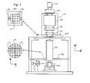
- FIG. 1depicts a lithographic projection apparatus according to an embodiment of the invention
- FIG. 2depicts the liquid reservoir of a first embodiment of the invention
- FIG. 3is similar to FIG. 2 showing an edge seal member on the substrate table according to an embodiment of the invention
- FIG. 4illustrates a second embodiment of the invention
- FIG. 5illustrates an alternative form of the second embodiment of the present invention
- FIG. 6illustrates a detail of the second embodiment of the present invention
- FIGS. 7 a - dillustrate four versions of a third embodiment of the present invention.
- FIG. 8 aillustrates a first version of a fourth embodiment of the present invention
- FIG. 8 billustrates a second version of the fourth embodiment
- FIG. 8 cillustrates a third version of the fourth embodiment
- FIG. 9illustrates in detail further aspects of the first version of the fourth embodiment of the present invention.
- FIG. 10illustrates a fifth embodiment of the present invention
- FIG. 11illustrates a sixth embodiment of the present invention
- FIG. 12illustrates in plan the substrate and edge seal member of a seventh embodiment of the present invention
- FIG. 13illustrates a cross section through the seventh embodiment of the present invention
- FIG. 14illustrates a detail of the seventh embodiment of the present invention
- FIG. 15illustrates in detail a further arrangement of the seventh embodiment
- FIG. 16illustrates an eighth embodiment of the present invention.
- FIG. 17illustrates a ninth embodiment of the present invention
- FIG. 18illustrates a tenth embodiment of the present invention
- FIG. 19illustrates an eleventh embodiment of the present invention
- FIG. 20illustrates a twelfth embodiment of the present invention
- FIG. 21illustrates a thirteenth embodiment of the present invention
- FIG. 22illustrates an alternative liquid supply system according to an embodiment of the invention.
- FIG. 23illustrates, in plan, the system of FIG. 22 .
- FIG. 1schematically depicts a lithographic projection apparatus according to a particular embodiment of the invention.
- the apparatuscomprises:
- the apparatusis of a transmissive type (e.g. has a transmissive mask). However, in general, it may also be of a reflective type, for example (e.g. with a reflective mask). Alternatively, the apparatus may employ another kind of patterning device, such as a programmable mirror array of a type as referred to above.
- the source LA(e.g. an excimer laser) produces a beam of radiation.
- This beamis fed into an illumination system (illuminator) IL, either directly or after having traversed conditioning means, such as a beam expander Ex, for example.
- the illuminator ILmay comprise adjusting means AM for setting the outer and/or inner radial extent (commonly referred to as ⁇ -outer and ⁇ -inner, respectively) of the intensity distribution in the beam.
- ⁇ -outer and ⁇ -innercommonly referred to as ⁇ -outer and ⁇ -inner, respectively
- itwill generally comprise various other components, such as an integrator IN and a condenser CO.
- the beam PB impinging on the mask MAhas a desired uniformity and intensity distribution in its cross-section.
- the source LAmay be within the housing of the lithographic projection apparatus (as is often the case when the source LA is a mercury lamp, for example), but that it may also be remote from the lithographic projection apparatus, the radiation beam which it produces being led into the apparatus (e.g. with the aid of suitable directing mirrors); this latter scenario is often the case when the source LA is an excimer laser.
- the current invention and claimsencompass both of these scenarios.
- the beam PBsubsequently intercepts the mask MA, which is held on a mask table MT. Having traversed the mask MA, the beam PB passes through the lens PL, which focuses the beam PB onto a target portion C of the substrate W. With the aid of the second positioning means (and interferometric measuring means IF), the substrate table WT can be moved accurately, e.g. so as to position different target portions C in the path of the beam PB. Similarly, the first positioning means can be used to accurately position the mask MA with respect to the path of the beam PB, e.g. after mechanical retrieval of the mask MA from a mask library, or during a scan.
- the object tables MT, WTwill be realized with the aid of a long-stroke module (course positioning) and a short-stroke module (fine positioning), which are not explicitly depicted in FIG. 1 .
- the mask table MTmay just be connected to a short stroke actuator, or may be fixed.
- the depicted apparatuscan be used in two different modes:
- step modethe mask table MT is kept essentially stationary, and an entire mask image is projected at one time (i.e. a single “flash”) onto a target portion C.
- the substrate table WTis then shifted in the x and/or y directions so that a different target portion C can be irradiated by the beam PB;
- a relatively large target portion Ccan be exposed, without having to compromise on resolution.
- FIG. 2shows a liquid reservoir 10 between the projection system PL and the substrate W which is positioned on the substrate stage WT.
- the liquid reservoir 10is filled with a liquid 11 having a relatively high refractive index, e.g. water, provided via inlet/outlet ducts 13 .
- the liquidhas the effect that the radiation of the projection beam is a shorter wavelength in the liquid than in air or in a vacuum, allowing smaller features to be resolved. It is well known that the resolution limit of a projection system is determined, inter alia, by the wavelength of the projection beam and the numerical aperture of the system. The presence of the liquid may also be regarded as increasing the effective numerical aperture. Furthermore, at fixed numerical aperture, the liquid is effective to increase the depth of field.
- the reservoir 10forms, in an embodiment, a contactless seal to the substrate W around the image field of the projection system PL so that the liquid is confined to fill the space between the substrate's primary surface, which faces the projection system PL, and the final optical element of the projection system PL.
- the reservoiris formed by a seal member 12 positioned below and surrounding the final element of the projection system PL.
- the liquid supply systemprovides liquid on only a localized area of the substrate.
- the seal member 12forms part of the liquid supply system for filling the space between the final element of the projection system PL and the substrate with a liquid. This liquid is brought into the space below the projection system PL and within the seal member 12 .
- the seal member 12in an embodiment extends a little above the bottom element of the projection system PL and the liquid rises above the final element so that a buffer of liquid is provided.
- the seal member 12has an inner periphery that at the upper end closely conforms to the shape of the projection system PL or the final element thereof and may, e.g. be round. At the bottom the inner periphery closely conforms to the shape of the image field, e.g. rectangular, though this is not necessarily so.
- the seal memberis substantially stationary in the XY plane relative to the projection system PL though there may be some relative movement in the Z direction (in the direction of the optical axis).
- a sealis formed between the seal member and the surface of the substrate. This seal is desired to be a contactless seal and may be a gas seal.
- the liquid 11is confined in the reservoir 10 by a seal device 16 .
- the seal deviceis a contactless seal i.e. a gas seal.
- the gas sealis formed by gas, e.g. air or synthetic air, provided under pressure via inlet 15 to the gap between seal member 12 and substrate W and extracted by first outlet 14 .
- the over pressure on the gas inlet 15 , vacuum level or under pressure on the first outlet 14 and the geometry of the gapare arranged so that there is a high-velocity gas flow inwards towards the optical axis of the apparatus that confines the liquid 11 .
- some liquidis likely to escape, for example up the first outlet 14 .
- FIGS. 22 and 23also depict a liquid reservoir defined by inlet(s) IN, outlet(s) OUT, the substrate W and the final element of projection system PL.
- the liquid supply system illustrated in FIGS. 22 and 23comprising inlet(s) IN and outlet(s) OUT, supplies liquid to the primary surface of the substrate in a localized area between the final element of the projection system and the substrate and can suffer from loss of liquid at the substrate edge.
- the liquid supply systemcan comprise that as described in relation to FIG. 2 and FIGS. 22 and 23 .
- a problem with the liquid supply arrangement illustrated in FIGS. 2 , 22 and 23occurs when imaging edge portions of the substrate W. This is because when the substrate W edge is positioned underneath the projection system PL one of the constraining walls (the substrate W) of the liquid supply system (the bottom one as illustrated) is removed thereby allowing immersion liquid to escape.
- the embodiments described hereincan be used with any other type of liquid supply system.
- FIG. 3illustrates how the edge portion of a substrate W may be imaged without catastrophic loss of immersion liquid from the liquid supply system.
- the edge seal member 17has an upper (as illustrated) primary surface substantially co-planar with the upper primary surface of substrate W and is closely adjacent to the edge of the substrate W so that there is no sudden loss of liquid as the edge of the substrate moves under the projection system PL. Some liquid loss into the gap may still occur.
- FIGS. 2 and 3there are arrangements in which the whole construction illustrated in FIGS. 2 and 3 is positioned upside down so that it is the lower surfaces of the edge seal member and the substrate which face the projection system and which are substantially co-planar. The surfaces are therefore referred to as the primary surfaces which face the projection system PL rather than upper surfaces. References herein to upper surfaces and lower surfaces may be also appropriately considered as references to lower and upper surfaces respectively in an upside-down configuration.
- the liquid supply systeme.g. reservoir 10
- the liquid supply systemcan be positioned over the edge of the substrate W and can even be moved completely off the substrate W. This enables edge portions of the substrate W to be imaged.
- the edge seal member 17may form an integral part of the substrate table WT (as illustrated in FIG. 4 as edge seal member 117 ) or may be temporarily mounted relative to the remainder of the substrate table by the use of, for example, vacuum suction or through use of electromagnetic forces.
- the edge seal member 17is moveable relative to the remainder of the substrate table (as illustrated in FIGS. 5 and 6 ) such that the height above the substrate table WT of the primary surface of the edge seal member 17 may be adjusted such that it is substantially co-planar with the primary surface of the substrate W. In this way the same edge seal member 17 may be used for different thicknesses of substrate W (thickness tolerance is about 25 ⁇ m though the embodiment can account for up to about 0.2 mm variation).
- the positioning mechanism for the edge seal member 17may be through use of piezoelectric elements or electromagnetism, worm gear, etc. A suitable mechanism is described in relation to the second embodiment described below.
- the edge seal member 17may be formed of several individual segments, each of which surrounds a portion of the edge of the substrate W.
- FIGS. 4 to 6A second embodiment is illustrated in FIGS. 4 to 6 and is the same or similar as the first embodiment except as described below.
- an edge liquid supply systemprovides liquid to a reservoir 30 via a port 40 .
- the liquid in the reservoir 30is optionally the same as the immersion liquid in the liquid supply system.
- the reservoir 30is positioned on the opposite side of the substrate W to the projection system PL and adjacent the edge of the substrate W and the edge of the edge seal member 17 , 117 .
- the edge seal member 17is comprised of an element which is separate to the substrate table WT whereas in FIG. 4 the edge seal member 117 is provided by an integral portion of the substrate table WT.
- the substrate Wis supported on the substrate table WT by a so-called pimple table 20 .
- the pimple table 20comprises a plurality of projections on which the substrate W rests.
- the substrate Wis held in place by, e.g., a vacuum source sucking the substrate onto the top surface of the substrate table WT.
- a vacuum sourcesucking the substrate onto the top surface of the substrate table WT.
- the mechanism 170 shown in FIG. 5 for moving the edge seal member 17 relative to the remainder of the substrate table WTis illustrated in detail in FIG. 6 .
- the reason for moving the edge seal member 17 in this wayis so that its primary surface can be made to be substantially co-planar with the primary surface of the substrate W. This allows a smooth movement of the liquid supply system over edge portions of the substrate W so that the bottom inner periphery of the liquid supply system can be moved to positions partly on the primary surface of substrate W and partly on the primary surface of the edge seal member 17 .
- a level sensor(not illustrated) is used to detect the relative heights of the primary surfaces of the substrate W and the edge seal member 17 . Based on the results of the level sensor, control signals are sent to the actuator 171 in order to adjust the height of the primary surface of the edge seal member 17 .
- a closed loop actuatorcould also be used for this purpose.
- the actuator 171is a rotating motor which rotates a shaft 176 .
- the shaft 176is connected to a circular disc at the end distal to the motor 171 .
- the shaft 176is connected away from the centre of the disc.
- the discis located in a circular recess in a wedge portion 172 .
- Ball bearingsmay be used to reduce the amount of friction between the circular disc and the sides of the recess in the wedge portion 172 .
- the motor 171is held in place by leaf springs 177 .
- On actuation of the motorthe wedge portion is driven to the left and right as illustrated (i.e. in the direction of the slope of the wedge portion) because of the excentre position of the shaft 176 in the disc.
- the motoris prevented from moving in the same direction as the direction of movement of the wedge portion 172 by the springs 177 .
- the wedge portion 172moves left and right as illustrated in FIG. 6 , its top surface 175 (which is the surface of the wedge which is sloped in relation to the primary surface of the edge seal member 17 ) contacts the bottom sloped surface of a further wedge member 173 which is fixed to the bottom of the edge seal member 17 .
- the edge seal member 17is prevented from moving in the direction of movement of the wedge member 172 so that when the wedge member 172 moves left and right the edge seal member 17 is lowered and raised respectively. Some biasing of the edge seal member 17 towards the substrate table WT may be necessary.
- the further wedge member 173could be replaced by an alternative shape, for example a rod positioned perpendicularly to the direction of movement of the wedge 172 . If the coefficient of friction between the wedge member 172 and the further wedge member 173 is greater than the tangent of the wedge angle then the actuator 170 is self-braking meaning that no force is required on the wedge member 172 to hold it in place. This is advantageous as the system will then be stable when the actuator 171 is not actuated. The accuracy of the mechanism 170 is of the order of a few ⁇ m.
- a mechanismmay be provided to adjust the height of the substrate W or the member supporting the substrate W so that the primary surfaces of the edge seal member 17 , 117 and the substrate can be made substantially co-planar.
- a third embodimentis illustrated in FIG. 7 and is the same or similar as the first embodiment except as described below.
- a vacuum port 46 connected to a vacuum sourceis provided underneath and adjacent edge portions of the edge seal member 117 and the substrate W on the opposite side of the substrate W to the projection system PL.
- the port 46is annular and formed by a continuous groove but may be discontinuous i.e. a discrete number of openings arranged in a circular pattern. In its simplest form the embodiment may work only with that vacuum supply via port 46 .
- the basic ideacan be improved by the provision of a substrate table WT as illustrated in detail in FIG. 7 a which illustrates a first version of the third embodiment.
- a portion 48 of the substrate table WTextends from the edge of the edge seal portion 117 radially inwardly so that it is positioned below the substrate table W on the other side of the substrate W to the projection system PL. Any immersion liquid which leaks through the gap between the portion 48 and the substrate W is attracted towards the vacuum source via port 46 .
- a channel 42is provided radially inwardly of the vacuum source also under the substrate W and is connected to a gas source. This may be a gas at a pressure greater than atmospheric pressure or it may be that the channel 42 is simply open to the atmosphere. This creates a flow of gas radially outwardly below the substrate W between the portion 48 of substrate table WT below the substrate W and the pimple table 20 .
- the pimple table 20has its own vacuum source to hold the substrate in place.
- any liquid escaping between edge seal member 117 and the substrate Wis pulled towards an annular compartment 44 (roughly 3 ⁇ 3 mm in cross section) in fluid connection with the vacuum source.
- the compartment 44is positioned between an annular port 47 open to the gap and the port 46 connected to the vacuum source.
- the compartmenthelps in establishing uniform flow around the periphery.
- the channel 42is connected to a continuous annular groove (shown as a widening of the duct).
- the compartment 44 , port 47 , and/or the groove of channel 42need not be annular and can be other appropriate shapes or configurations.
- the gap between the portion 48 of substrate table WT and the substrate Wis of the order of up to 100 ⁇ m (though the gap may not exist i.e. is zero), which prevents a high flow rate of liquid through the gap due to capillary action.
- the height of the portion 45 of the substrate table WT between the groove connected to channel 42 and compartment 44is such that the distance between the bottom of the substrate W and the top of that portion 45 (indicated as distance D 1 in FIG. 7 a ) is typically of the order of 100 ⁇ m and is chosen such that a uniform gas flow of in the region of at least 1 m/s is achievable with a pressure loss of less than 0.5 bar.
- Such an arrangementensures that only very little, if any, liquid passes through the gap D 1 and interferes with the pimple table 20 . Other values will also work.
- a first version of the third embodiment illustrated in FIG. 7 amay suffer from deflection of the outer 10 mm or so of the substrate W. As can be seen from FIG. 7 a this area is unsupported even though, as said above, portion 45 can be extended to underneath the substrate W where it supports the substrate W. However, at the very outer radius both the weight of the substrate W and the capillary force of liquid between the substrate W and portion 48 of the substrate table WT can still deflect the edge of the substrate W. This may be deleterious. Solutions to this problem are illustrated in FIGS. 7 b - d which illustrate second through fourth versions of the third embodiment.
- the portion 48has at least one set of burls 348 positioned around and near to the edge of the periphery of the substrate W (typically in a circular pattern). As the burls 348 are discrete, immersion liquid can still seep between the portion 48 and the substrate W but the weight of the substrate W is supported by the at least one set of burls 348 .
- the burls 348have a smaller height than the burls of the pimple table 20 which compensates for the difference in the force downwards on the substrate W caused by the vacuum 22 of the pimple table 20 compared to the force on the substrate W at the edge in the vicinity of burls 348 .
- the calculationmust take the stiffness of the burls into account and if the burls are manufactured from a low expansion material such as Zerodur, they should be about 80 nm less high than the burls of the pimple table 20 .
- the gap between the portion 48 and the bottom of the substrate Wis in an embodiment about 20 ⁇ m.
- portion 45is similar in shape to that of the first version.
- an alternativehas a ring or circular pattern of burls 345 positioned above portion 45 .
- the discrete nature of the burls 345allows gas from channel 42 to be sucked into the compartment 44 .
- These burls 345are also about 80 nm less high than the burls of the pimple table 20 .
- gap D 1 in between the burls 345is about 50 ⁇ m.
- the burls 345may be formed by the pimple table 20 and need not necessarily be part of the substrate table WT.
- FIGS. 7 c and 7 dillustrate two further versions of the third embodiment.
- FIG. 7 cillustrates a third version of the third embodiment in which the gas seal is formed by members of the pimple table 20 .
- the portion 45 of the first and second versionsis formed by a (annular) portion of the pimple table 2045 and portion 48 of the first and second versions is formed by (annular) portion 2048 of the pimple table 20 .
- Passages 2042 , 2047 equivalent to 42 and 47are formed between the portions 20 , 2045 and 2048 .
- a fourth version of the third embodiment illustrated in FIG. 7 dno inlet channel 42 is provided and gas flows from the pimple table 20 into (annular) port 47 .
- This versionhas an advantage that a more stable pressure is experienced between the substrate W and the pimple table 20 because the pimple table 20 does not need its own vacuum source.
- extra passage 2047 which is provided in the third versionis no longer necessary and only passage 2042 is used.
- a gas sourcemay be required under the pimple table 20 (perhaps the more usual vacuum port in the substrate table under the pimple table can be used for this purpose) so that a flow of gas outwards can be established.
- FIGS. 8 and 9A fourth embodiment is illustrated in FIGS. 8 and 9 and is the same or similar as the first embodiment except as described below.
- This embodimentis described in relation to an edge seal member 117 which is an integral part of the substrate table WT. However, this embodiment is equally applicable to an edge seal member 17 which is movable relative to the substrate table WT.
- a further edge seal member 500is used to bridge the gap between the edge seal member 117 and the substrate W.
- the further edge seal memberis affixed to the edge seal member 117 .
- the further edge seal member 500is removably attachable against the surface of the substrate W opposite the primary surface.
- the further edge seal member 500can be a flexible edge seal member which is actuatable to contact the under surface of the substrate W. When the flexible edge seal member 500 is deactivated it falls away from the substrate under gravity. The way this may be achieved is illustrated in FIG. 9 and is described below.
- a port 46 connected to a low pressure sourcemay be provided under the substrate W adjacent edges of the edge seal member 117 and the substrate W in some or all of the versions of this embodiment.
- the design of the area under the substratecould be the same as that of the third embodiment.
- the same systemcan be used for sensors such as a transmission image sensor (TIS) on the substrate table as opposed for the substrate W.
- TIStransmission image sensor
- the edge seal member 500can be permanently attached to the sensor, for example using glue.
- edge seal member 500can be arranged to engage with the top surface of the object (that surface closest to the projection system PL) rather than the bottom surface. Also, the further edge seal member 500 may be provided attached to or near the top surface of the edge seal member 117 as opposed to under the edge seal member 117 as is illustrated in FIG. 8 a.
- FIG. 8 bA second version of this embodiment is illustrated in FIG. 8 b .
- Two further edge seal members 500 a , 500 bare used.
- the first of these edge seal members 500 ais the same as in the first version.
- the second of these edge seal members 500 bis affixed to the substrate table 20 i.e. underneath the substrate W and extends with its free end radially outwardly from its attachment point.
- the second further edge seal member 500 bclamps the first further edge seal member 500 a against the substrate W.
- Compressed gascan be used to deform or move the second further edge seal member 500 b.
- FIG. 8 cA third version of this embodiment is shown in FIG. 8 c .
- the third versionis the same as the second version except the first further edge seal member 500 c clamps the second further edge seal member 500 d to the substrate W. This avoids, for example, the need for the compressed gas of the second version.
- a channel 510is formed in the elongate direction of a flexible further edge seal member 500 (which in an embodiment is an annular ring) and (a) discrete port(s) are provided in an upper surface of the flexible further edge seal member which faces the projection system PL and the underside of the substrate W.
- a vacuum source 515By connecting a vacuum source 515 to the duct 510 the flexible further edge seal member can be made to abut the substrate W by suction.
- the vacuum source 515is disconnected or switched off, the flexible further edge seal member 500 drops under gravity and/or pressure from port 46 to assume the position shown in dotted lines in FIG. 9 .
- a flexible further edge seal member 500is formed with a mechanical pre-load such that it contacts the substrate W when the substrate is placed on the pimple table 20 and the flexible further edge seal member 500 deforms elastically so that it applies a force upwards on the substrate W to thereby make a seal.
- a flexible further edge seal member 500may be forced against the substrate W by an overpressure generated by pressurised gas on port 46 .
- a flexible further edge seal member 500may be fashioned from any flexible, radiation and immersion liquid resistant, non-contaminating material, for example, steel, glass e.g. Al 2 O 3 , ceramic material e.g. SiC, silicon, Teflon, low expansion glasses (e.g. ZerodurTM or ULETM), carbon fibre epoxy or quartz and is typically between 10 and 500 ⁇ m thick, in an embodiment between 30 and 200 ⁇ m or 50 to 150 ⁇ m in the case of glass. With a flexible further edge seal member 500 of this material and these dimensions, the typical pressure to be applied to the duct 510 is approximately 0.1 to 0.6 bar.
- a fifth embodimentis illustrated in FIG. 10 and is the same or similar as the first embodiment except as described below.
- This embodimentis described in relation to an edge seal member 117 which is an integral part of the substrate table WT. However, this embodiment is equally applicable to an edge seal member 17 which is movable relative to the substrate table WT.
- the gap between the edge seal member 117 and the substrate Wis filled with a further edge seal member 50 .
- the further edge seal memberis a flexible further edge seal member 50 which has a top surface which is substantially co-planar with the primary surfaces of the substrate W and the edge seal member 117 .
- the flexible further edge seal member 50is made of a compliant material so that minor variations in the diameter/width of substrate W and in the thickness of the substrate W can be accommodated by deflections of the flexible further edge seal member 50 .
- the liquid supply system operationis not upset when it passes over the edge of the substrate W so that disturbance forces are not generated in the liquid supply system.
- the flexible further edge seal member 50is in contact with a surface of the substrate W opposite the primary surface of the substrate W, at an edge portion.
- This contacthas two functions. First the fluid seal between the flexible further edge seal member 50 and the substrate W may be improved. Second, the flexible further edge seal member 50 applies a force on the substrate W in a direction away from the pimple table 20 .
- the substrate Wis held on the substrate table WT by, e.g. vacuum suction, the substrate can be held securely on the substrate table.
- the force produced by the flexible further edge seal member 50 on the substrate Wis effective to push the substrate W off the substrate table WT thereby aiding loading and unloading of substrates W.
- the flexible further edge seal member 50is made of a radiation and immersion liquid resistant material such as PTFE.
- FIG. 11illustrates a sixth embodiment which is the same or similar as the first embodiment except as described below.
- This embodimentis described in relation to an edge seal member 117 which is an integral part of the substrate table WT. However, this embodiment is equally applicable to an edge seal member 17 which is movable relative to the substrate table WT.
- the sixth embodimentillustrates how the pimple table 20 can be decoupled from the liquid supply system between the substrate W and the edge seal member 117 . This is done by positioning an opening exposed to the atmosphere 65 between the edge of the substrate W and the vacuum holding the substrate W on the substrate table WT and associated with the pimple table 20 .
- a layer 60positioned on the opposite side of the substrate W to the projection system PL and under the substrate at its edge leaving a gap between the substrate W and the layer 60 of about 10 ⁇ m, comprises any material which is hydrophobic such as TeflonTM, silicon rubber, or other plastics material. Inorganic materials are desired because they have better radiation resistance. In this way, liquid which finds its way into the gap between the substrate W and the edge seal member 117 when the liquid supply system is positioned over the edge of the substrate W is repelled such that an effective seal is formed and liquid does not find its way to the pimple table 20 .
- the immersion liquidhas a contact angle of at least 90° with the hydrophobic layer 60 .
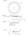
- a seventh embodimentwill be described with reference to FIGS. 12 to 15 .
- the seventh embodimentis the same or similar as the first embodiment except as described below.
- the edge seal member 17is annular with a central hole larger than the diameter of the circular substrate W.
- the shapes of the substrate W and edge seal member 17may be different than annular so long as the central hole of the edge seal member 17 is larger than the outer diameter/width of the substrate W. In this way, the edge seal member 17 may accommodate variations in the substrate W diameter/width.
- the edge seal member 17is movable on the substrate table WT such that when the liquid supply system moves towards an edge portion of the substrate W in order to expose it, the edge seal member 17 can be moved closely to abut that edge portion of the substrate W which is to be exposed. This is best illustrated in FIG. 13 where the left hand side of the substrate W is about to be exposed.
- the edge seal member 17is movable both in the plane of the primary surface of the substrate W and in an embodiment also in the Z direction (i.e. in the direction of the optical axis of the apparatus). In this way, the edge seal member 17 can be moved to the edge of the substrate W when required and can have the height of its top (primary) surface adjusted so that its primary surface is closely co-planar with the primary surface of the substrate W. This allows the liquid supply system to effectively contain the immersion liquid in its reservoir even when the edge of the substrate W is being imaged.
- a projection 175which has a top surface which is co-planar with the primary surface of the edge seal member 17 , i.e. the primary surface of the edge seal member 17 overhangs on an edge adjacent the substrate W so that the projection extends towards the optical axis of the apparatus.
- thisallows the gap between the primary surfaces of the substrate W and edge seal member 17 to be minimised even when the edge of the substrate W is slightly curved (i.e. the edge of the substrate W is not perpendicular to the primary surface).
- Another way of improving or reducing the gap between the edge seal member 17 and the substrate Wis to provide a further (flexible) edge seal member 177 between the edge of the edge seal member 17 closest to the substrate W and the substrate W. This is illustrated in FIG. 15 . This may be done with or without a projection 175 .
- a further flexible edge seal member 177can deform around the edge of the substrate W so as to form a tight seal with the substrate W.
- the further flexible edge seal member 177is attached to the edge seal member 17 .
- the further flexible edge seal member 177has an upper surface which is substantially co-planar with the primary surfaces of the substrate W and the edge seal member 17 .
- FIG. 16illustrates an eighth embodiment which is the same or similar as the first embodiment except as described below.
- This embodimentis described in relation to an edge seal member 117 which is an integral part of the substrate table WT. However, this embodiment is equally applicable to an edge seal member 17 which is movable relative to the substrate table WT.
- the eighth embodimentincludes a further edge seal member 100 for bridging the gap between the edge seal member 117 and the substrate W.
- the further edge seal member 100is a gap seal member which is positioned on the primary surfaces of the substrate W and the edge seal member 117 to span the gap between the substrate W and edge seal member 117 .
- the gap seal member 100will also be circular (annular).
- the gap seal member 100may be held in place by the application of a vacuum 105 to its underside (that is a vacuum source exposed through a vacuum port on the primary surface of the edge seal member 117 ).
- the liquid supply systemcan pass over the edge of the substrate W without the loss of liquid because the gap between the substrate W and the edge seal member 117 is covered over by the gap seal member 100 .
- the gap seal member 100can be put in place and removed by the substrate handler so that standard substrates and substrate handling can be used. Alternatively, the gap seal member 100 can be kept at the projection system PL and put in place and removed by appropriate mechanisms (e.g. a substrate handling robot).
- the gap seal member 100should be stiff enough to avoid deformation by the vacuum source.
- the gap seal member 100is less than 50, in an embodiment 30 or 20 or even 10 ⁇ m thick to avoid contact with the liquid supply system, but should be made as thin as possible.
- the gap seal member 100is advantageously provided with tapered edges 110 in which the thickness of the gap seal member 100 decreases towards the edges. This gradual transition to the full thickness of the gap seal member ensures that disturbance of the liquid supply system is reduced when it passes on top of the gap seal member 100 .
- the gap seal member 100can be glued in place (at either end) with a glue which does not dissolve in the immersion liquid.
- the gluecan alternatively be positioned at the junction of the edge seal member 117 , the object and the gap seal member 100 .
- the gap seal member 100can be positioned underneath the object and an overhang of the edge seal member 117 .
- the objectmay be shaped with an overhang also, if necessary.
- the gap seal member 100can have a passage provided through it, from one opening in a surface in contact with the edge seal member 117 to another opening in a surface in contact with the object. By positioning one opening in fluid communication with vacuum 105 , the gap seal member 100 can then be kept tightly in place.
- a ninth embodimentwill be described with reference to FIG. 17 .
- the solution shown in FIG. 17bypasses some of the problems associated with imaging edge portions of the substrate W as well as allows a transmission image sensor (TIS) 220 (or other sensor) to be illuminated by the projection system PL under the same conditions as the substrate W.
- TIStransmission image sensor
- the ninth embodimentuses the liquid supply system described with respect to the first embodiment. However, rather than confining the immersion liquid in the liquid supply system under the projection system PL on its lower side with the substrate W, the liquid is confined by an intermediary plate 210 which is positioned between the liquid supply system and the substrate W. The spaces 222 , 215 between the intermediary plate 210 and the TIS 220 and the substrate W are also filled with liquid 111 . This may either be done by two separate space liquid supply systems via respective ports 230 , 240 as illustrated or by the same space liquid supply system via ports 230 , 240 .
- the space 215 between the substrate W and the intermediary plate 210 and the space 222 between the transmission image sensor 220 and the intermediary plate 210are both filled with liquid and both the substrate W and the transmission image sensor can be illuminated under the same conditions.
- Portions 200provide a support surface or surfaces for the intermediary plate 210 which may be held in place by vacuum sources.
- the intermediary plate 210is made of such a size that it covers all of the substrate W as well as the transmission image sensor 220 . Therefore, no edges need to be traversed by the liquid supply system even when the edge of the substrate W is imaged or when the transmission image sensor is positioned under the projection system PL.
- the top surface of the transmission image sensor 220 and the substrate Ware substantially co-planar.
- the intermediate plate 210can be removable. It can, for example, be put in place and removed by a substrate handling robot or other appropriate mechanism.
- FIG. 18shows a modification of the liquid supply system which is applicable to any other embodiment described herein which is effective to increase the size of gap the immersion liquid can span before sudden liquid loss.
- a plurality of capillaries 600are provided between the liquid supply system (e.g. seal member 12 ) and the projection system PL. These capillaries extend generally upwardly, i.e. away from the substrate W. If the capillaries have a radius r, the liquid film thickness h, which can be supported by the capillary, is given by the formula:
- ⁇is the interfacial tension
- ⁇the contact angle between the liquid and the capillaries W and ⁇ the liquid density.
- the capillaries 600may be provided by substantially straight ducts with a substantially circular cross-section or by other shaped ducts.
- the capillariesmay be made up of voids in a porous material.
- FIG. 19shows an eleventh embodiment which is the same as the first embodiment except as described below.
- the object on the substrate table WTis a sensor 220 such as a transmission image sensor (TIS).
- a bead of glue 700which is undissolvable and unreactable with the immersion fluid is positioned between the edge seal member 117 and the sensor 220 .
- the glueis covered by immersion fluid in use.
- a twelfth embodimentis described with reference to FIGS. 20 and 21 .
- the twelfth embodimentit is a sensor 220 which is being sealed to the substrate table WT.
- a vacuum 46is provided adjacent the gap with an opening passage 47 and a chamber 44 for taking away any immersion liquid which should find its way through the gap between the edge seal member 117 and the edge of the sensor 220 .
- the vacuum 46is provided in the substrate table WT under an overhang portion of the object 220 .
- the passage 47is provided in an overhanging inwardly protruding portion of the substrate table WT.
- a bead of glue 700is positioned at the inner most edge of the protruding portion between the substrate table WT and the object 220 . If no bead of glue 700 is provided, a flow of gas from underneath the object 220 helps seal the gap between the sensor 220 and the substrate table WT.
- the vacuum 46 , compartment 44 and passage 47are provided in the object 220 itself under an inwardly protruding edge seal member 117 . Again there is the option of providing a bead of glue between the object 220 and the substrate table WT radially outwardly of the passage 47 .
- All of the above described embodimentsmay be used to seal around the edge of the substrate W.
- Other objects on the substrate table WTmay also need to be sealed in a similar way, such as sensors including sensors and/or marks which are illuminated with the projection beam through the liquid such as a transmission image sensor, an integrated lens interferometer and scanner (wavefront sensor) and spot sensor plates.
- sensorsincluding sensors and/or marks which are illuminated with the projection beam through the liquid
- Such objectsmay also include sensors and/or marks which are illuminated with non-projection radiation beams such as levelling and alignment sensors and/or marks.
- the liquid supply systemmay supply liquid to cover all of the object in such a case. Any of the above embodiments may be used for this purpose.
- the objectwill not need to be removed from the substrate table WT as, in contrast to the substrate W, the sensors do not need to be removed from the substrate table WT.
- the above embodimentsmay be modified as appropriate (e.g. the seals may not need to be moveable).
- each of the embodimentsmay be combined with one or more of the other embodiments as appropriate. Further, each of the embodiments (and any appropriate combination of embodiments) can be applied simply to the liquid supply system of FIG. 2 and FIGS. 19 and 20 without the edge seal member 17 , 117 as feasible and/or appropriate.
- edge seal member 117 and the top outer most edge of the sensor 220can be varied. For example, it may be advantageous to provide an overhanging edge seal member 117 or indeed an outer edge of the sensor 220 which is overhanging. Alternatively, an outer upper corner of the sensor 220 may be useful.
- seal member solutionit may be one in which a seal other than a gas seal is used. The description is not intended to limit the invention.
Landscapes
- Physics & Mathematics (AREA)
- General Physics & Mathematics (AREA)
- Health & Medical Sciences (AREA)
- Engineering & Computer Science (AREA)
- Environmental & Geological Engineering (AREA)
- Epidemiology (AREA)
- Public Health (AREA)
- Life Sciences & Earth Sciences (AREA)
- Atmospheric Sciences (AREA)
- Toxicology (AREA)
- Exposure And Positioning Against Photoresist Photosensitive Materials (AREA)
- Exposure Of Semiconductors, Excluding Electron Or Ion Beam Exposure (AREA)
Abstract
Description
- This application is a divisional application of U.S. patent application Ser. No. 11/710,408, entitled “Lithographic Apparatus And Device Manufacturing Method”, filed on Feb. 26, 2007, which is a divisional application of U.S. application Ser. No. 10/705,804, filed Nov. 12, 2003, which claims priority from European patent applications EP 02257822.3, filed Nov. 12, 2002, and EP 03253636.9, filed Jun. 9, 2003, each of which are incorporated herein in their entirety by reference.
- The present invention relates to immersion lithography.
- The term “patterning device” as here employed should be broadly interpreted as referring to means that can be used to endow an incoming radiation beam with a patterned cross-section, corresponding to a pattern that is to be created in a target portion of the substrate; the term “light valve” can also be used in this context. Generally, the said pattern will correspond to a particular functional layer in a device being created in the target portion, such as an integrated circuit or other device (see below). Examples of such a patterning device include:
- A mask. The concept of a mask is well known in lithography, and it includes mask types such as binary, alternating phase-shift, and attenuated phase-shift, as well as various hybrid mask types. Placement of such a mask in the radiation beam causes selective transmission (in the case of a transmissive mask) or reflection (in the case of a reflective mask) of the radiation impinging on the mask, according to the pattern on the mask. In the case of a mask, the support structure will generally be a mask table, which ensures that the mask can be held at a desired position in the incoming radiation beam, and that it can be moved relative to the beam if so desired.
- A programmable mirror array. One example of such a device is a matrix-addressable surface having a viscoelastic control layer and a reflective surface. The basic principle behind such an apparatus is that (for example) addressed areas of the reflective surface reflect incident light as diffracted light, whereas unaddressed areas reflect incident light as undiffracted light. Using an appropriate filter, the said undiffracted light can be filtered out of the reflected beam, leaving only the diffracted light behind; in this manner, the beam becomes patterned according to the addressing pattern of the matrix-addressable surface. An alternative embodiment of a programmable mirror array employs a matrix arrangement of tiny mirrors, each of which can be individually tilted about an axis by applying a suitable localized electric field, or by employing piezoelectric actuation means. Once again, the mirrors are matrix-addressable, such that addressed mirrors will reflect an incoming radiation beam in a different direction to unaddressed mirrors; in this manner, the reflected beam is patterned according to the addressing pattern of the matrix-addressable mirrors. The required matrix addressing can be performed using suitable electronic means. In both of the situations described hereabove, the patterning device can comprise one or more programmable mirror arrays. More information on mirror arrays as here referred to can be gleaned, for example, from U.S. Pat. No. 5,296,891 and U.S. Pat. No. 5,523,193, and PCT patent applications WO 98/38597 and WO 98/33096, which are incorporated herein by reference. In the case of a programmable mirror array, the said support structure may be embodied as a frame or table, for example, which may be fixed or movable as required.
- A programmable LCD array. An example of such a construction is given in U.S. Pat. No. 5,229,872, which is incorporated herein by reference. As above, the support structure in this case may be embodied as a frame or table, for example, which may be fixed or movable as required.
- For purposes of simplicity, the rest of this text may, at certain locations, specifically direct itself to examples involving a mask and mask table; however, the general principles discussed in such instances should be seen in the broader context of the patterning device as hereabove set forth.
- Lithographic projection apparatus can be used, for example, in the manufacture of integrated circuits (ICs). In such a case, the patterning device may generate a circuit pattern corresponding to an individual layer of the IC, and this pattern can be imaged onto a target portion (e.g. comprising one or more dies) on a substrate (silicon wafer) that has been coated with a layer of radiation-sensitive material (resist). In general, a single wafer will contain a whole network of adjacent target portions that are successively irradiated via the projection system, one at a time. In current apparatus, employing patterning by a mask on a mask table, a distinction can be made between two different types of machine. In one type of lithographic projection apparatus, each target portion is irradiated by exposing the entire mask pattern onto the target portion at one time; such an apparatus is commonly referred to as a wafer stepper. In an alternative apparatus—commonly referred to as a step-and-scan apparatus—each target portion is irradiated by progressively scanning the mask pattern under the projection beam in a given reference direction (the “scanning” direction) while synchronously scanning the substrate table parallel or anti-parallel to this direction; since, in general, the projection system will have a magnification factor M (generally <1), the speed V at which the substrate table is scanned will be a factor M times that at which the mask table is scanned. More information with regard to lithographic devices as here described can be gleaned, for example, from U.S. Pat. No. 6,046,792, incorporated herein by reference.
- In a manufacturing process using a lithographic projection apparatus, a pattern (e.g. in a mask) is imaged onto a substrate that is at least partially covered by a layer of radiation-sensitive material (resist). Prior to this imaging step, the substrate may undergo various procedures, such as priming, resist coating and a soft bake. After exposure, the substrate may be subjected to other procedures, such as a post-exposure bake (PEB), development, a hard bake and measurement/inspection of the imaged features. This array of procedures is used as a basis to pattern an individual layer of a device, e.g. an IC. Such a patterned layer may then undergo various processes such as etching, ion-implantation (doping), metallization, oxidation, chemo-mechanical polishing, etc., all intended to finish off an individual layer. If several layers are required, then the whole procedure, or a variant thereof, will have to be repeated for each new layer. Eventually, an array of devices will be present on the substrate (wafer). These devices are then separated from one another by a technique such as dicing or sawing, whence the individual devices can be mounted on a carrier, connected to pins, etc. Further information regarding such processes can be obtained, for example, from the book “Microchip Fabrication: A Practical Guide to Semiconductor Processing”, Third Edition, by Peter van Zant, McGraw Hill Publishing Co., 1997, ISBN 0-07-067250-4, incorporated herein by reference.
- For the sake of simplicity, the projection system may hereinafter be referred to as the “lens”; however, this term should be broadly interpreted as encompassing various types of projection system, including refractive optics, reflective optics, and catadioptric systems, for example. The radiation system may also include components operating according to any of these design types for directing, shaping or controlling the projection beam of radiation, and such components may also be referred to below, collectively or singularly, as a “lens”. Further, the lithographic apparatus may be of a type having two or more substrate tables (and/or two or more mask tables). In such “multiple stage” devices the additional tables may be used in parallel, or preparatory steps may be carried out on one or more tables while one or more other tables are being used for exposures. Dual stage lithographic apparatus are described, for example, in U.S. Pat. No. 5,969,441 and PCT patent application WO 98/40791, incorporated herein by reference.
- It has been proposed to immerse the substrate in a lithographic projection apparatus in a liquid having a relatively high refractive index, e.g. water, so as to fill a space between the final optical element of the projection lens and the substrate. The point of this is to enable imaging of smaller features because the exposure radiation will have a shorter wavelength in the liquid than in air or in a vacuum. (The effect of the liquid may also be regarded as increasing the effective NA of the system).
- However, submersing the substrate or substrate and substrate table in a bath of liquid (see, for example, U.S. Pat. No. 4,509,852, hereby incorporated in its entirety by reference) may mean that there is a large body of liquid that must be accelerated during a scanning exposure. This may require additional or more powerful motors and turbulence in the liquid may lead to undesirable and unpredictable effects.
- One of the solutions proposed is for a liquid supply system to provide liquid on only a localized area of the substrate and in between the final element of the projection lens and the substrate (the substrate generally has a larger surface area than the final element of the projection system). One way which has been proposed to arrange for this is disclosed in PCT patent application WO 99/49504, hereby incorporated in its entirety by reference. As illustrated in
FIGS. 22 and 23 , liquid is supplied by at least one inlet IN onto the substrate, preferably along the direction of movement of the substrate relative to the final element, and is removed by at least one outlet OUT after having passed under the projection system. That is, as the substrate is scanned beneath the element in a −X direction, liquid is supplied at the +X side of the element and taken up at the −X side.FIG. 23 shows the arrangement schematically in which liquid is supplied via inlet IN and is taken up on the other side of the element by outlet OUT which is connected to a low pressure source. In the illustration ofFIG. 22 the liquid is supplied along the direction of movement of the substrate relative to the final element, though this does not need to be the case. Various orientations and numbers of in- and out-lets positioned around the final element are possible, one example is illustrated inFIG. 23 in which four sets of an inlet with an outlet on either side are provided in a regular pattern around the final element. - Difficulties in large loss of liquid from the liquid supply system can arise with the system described above and any other systems that provide liquid on only a localized area of the substrate and between the projection system and the substrate when the localized area crosses over an edge of the substrate or other object.
- Accordingly, it may be advantageous to provide, for example, a lithographic projection apparatus in which liquid loss from the supply system is minimized during passage over an edge portion of the substrate or other object.
- According to an aspect, there is provided a lithographic projection apparatus comprising:
- a support structure configured to hold a patterning device, the patterning device configured to pattern a beam of radiation according to a desired pattern;
- a projection system configured to project the patterned beam onto a target portion of a substrate;
- a substrate table configured to hold the substrate, said substrate table comprising an edge seal member configured to at least partly surround an edge of at least one of said substrate and an object positioned on said substrate table and to provide a primary surface facing said projection system substantially co-planar with a primary surface of the said at least one of said substrate and said object; and
- a liquid supply system configured to provide a liquid, through which said beam is to be projected, in a space between said projection system and said at least one of said substrate and said object, wherein said liquid supply system provides liquid to a localized area of at least one of said object, said edge seal member and said substrate.
- Where applied to a substrate, the edge seal member surrounds a position on the substrate table where, in use, the substrate is to be placed, e.g., surrounding the chuck or pimple table on which the substrate is held. In this way the substrate can be positioned closely adjacent to the edge of the edge seal member such that as an edge of the substrate moves under the projection system there is no sudden loss of liquid from the space because there is no large gap for the liquid to flow through. The edge seal member may be an integral part of the substrate table or may be moveably mounted relative to the remainder of the substrate table. In the latter case, it can be arranged such that the gap between the edge seal member and the substrate can be varied and/or the height of the primary surface of the edge seal member can be varied to accommodate variations in substrate height or thickness, i.e., to ensure that the primary surface of the edge seal member is substantially coplanar with the primary surface of the substrate. The above may also be applied to an object on the substrate table such as a sensor, e.g., a projection beam sensor.
- In an embodiment, the substrate table comprises a gap seal member configured to abut or at least partly overlap, in the direction of the optical axis, both the edge seal member and said at least one of said substrate and said object. For example, in this way the gap between the edge seal member and a substrate (or an object), which is due to the size mismatch between the inner edge of the edge seal member and the outer edge of the substrate or object (which is necessary to accommodate slight variations in the diameter of the substrate or object), can be covered by the gap seal member. This further reduces the amount of liquid loss into the gap between the edge seal member and the substrate or object. In an embodiment, the gap seal member is configured to be in contact with the primary surfaces, thereby spanning the gap between the edge seal member and said at least one of said substrate and said object.
- If the gap seal member has inner and outer edges, at least one of the edges may be tapered such that the thickness of the gap seal member facing away from the edge seal member or said at least one of said substrate and said object decreases towards the edge of the gap seal member. This helps the liquid supply system move smoothly over the gap between the substrate or object and the edge seal member.
- A way to hold the gap seal member removably in place is to provide the substrate table with a vacuum port in the primary surface of said edge seal member.
- Another way to minimise the amount of liquid which escapes into the gap between the edge seal member and the substrate or object is to provide the substrate table with a hydrophobic layer facing edge portions of said edge seal member and the substrate or object on an opposite side of the edge seal member and the substrate or object to the projection system. Such a hydrophobic layer may be any material which exhibits hydrophobic properties, for example Teflon, silicon rubber or other plastics materials. Inorganic coatings are generally desired because they have better radiation resistance than organic coatings. In an embodiment, the liquid has a contact angle of greater than 90° with the hydrophobic layer. This reduces the chances of liquid seeping into the gap.
- According to an aspect, there is provided a lithographic projection apparatus comprising:
- a support structure configured to hold a patterning device, the patterning device configured to pattern a beam of radiation according to a desired pattern;
- a projection system configured to project the patterned beam onto a target portion of a substrate;
- a substrate table configured to hold the substrate, said substrate table comprising:
- an edge seal member configured to at least partly surround an edge of at least one of said substrate and an object positioned on said substrate table, and
- a further edge seal member configured to extend across the gap between said edge seal member and said at least one of said substrate and said object and to be in contact with said at least one of said substrate and said object; and
- a liquid supply system configured to provide a liquid, through which said beam is to be projected, in a space between said projection system and said at least one of said substrate and said object.
- In this way the gap between the edge seal member and the substrate or object is closed off so that there is no gap between the edge seal member and the substrate or object through which liquid from the liquid supply system can pass. This is particularly so if the further edge seal member is flexible in which case a better seal between the further edge seal member and the substrate or object is achievable.
- In an embodiment, the flexible further edge seal member is attached to the edge seal member and has a port, connected to a vacuum source, adjacent its end distal from said edge seal member, such that on actuation of said vacuum source, said flexible further edge seal member is deflectable upwards to contact against the substrate or object to form a seal between said flexible further edge seal member and the substrate or object due to the force generated by the vacuum source acting on the substrate or object. This allows the flexible further edge seal member to be actuatable to contact with the substrate or object and to be deactuatable so that it falls away from the substrate or object. The application of the vacuum ensures a good seal between the flexible further edge seal member and the substrate or object.
- In another embodiment, the flexible further edge seal member is disposed between the edge seal member and the substrate or object and with a surface substantially co-planar with the primary surfaces of the edge seal member and the substrate or object. In this way the gap between the edge seal member and the substrate or object can be sealed such that only small amounts of liquid can pass into the gap. In an embodiment, the flexible further edge seal member is shaped to contact the substrate or object on the surface opposite its primary surface and may be effective to apply a force to the substrate or the object away from the substrate table when the substrate or object is held on the substrate table. In the case of the substrate, the flexible further edge seal member in this way may help in the removal of the substrate from the substrate table after exposure of the substrate.
- According to an aspect, there is provided a lithographic projection apparatus comprising:
- a support structure configured to hold a patterning device, the patterning device configured to pattern a beam of radiation according to a desired pattern;
- a projection system configured to project the patterned beam onto a target portion of a substrate;
- a substrate table configured to hold the substrate, said substrate table comprising:
- an edge seal member configured to at least partly surround an edge of at least one of said substrate and an object positioned on said substrate table, and
- at least one of a vacuum port and a liquid supply port positioned to provide respectively a vacuum or liquid to the gap between said edge seal member and said at least one of said substrate and said object on a side opposite said projection system;
- a liquid supply system configured to provide a liquid, through which said beam is to be projected, in a space between said projection system and said at least one of said substrate and said object.
- In the case of a liquid supply port, no liquid can find its way into the gap between the edge seal member and the substrate or object from the space between the projection system and the substrate or object, because that gap is already filled with liquid. If the vacuum alternative is used, any liquid which does find its way into that gap will be removed and may be recycled. The provision of vacuum is advantageous when a gas seal member of a liquid supply system is used to keep the liquid in the space between the projection system and the substrate or object. This is because it can not only remove any liquid passing into the gap but also any gas from the gas seal member.
- Further, there may be provided a channel positioned radially inwardly of the vacuum port, the channel being connected to a gas source such that on actuation of the vacuum a flow of gas radially outwardly from said channel toward said vacuum can be established. Such a flow of gas can be used to ensure that any liquid which does reach the non-immersed side of the substrate or object is caught in the gas flow and transported away towards the vacuum.
- According to an aspect, there is provided a lithographic projection apparatus comprising:
- a support structure configured to hold a patterning device, the patterning device configured to pattern a beam of radiation according to a desired pattern;
- a projection system configured to project the patterned beam onto a target portion of a substrate;
- a substrate table configured to hold the substrate, said substrate table comprising a support surface configured to support an intermediary plate between said projection system and at least one of said substrate and an object positioned on said substrate table and not in contact with said at least one of said substrate and said object; and
- a liquid supply system configured to provide a liquid, through which said beam is to be projected, in a space between said projection system and said at least one of said substrate and said object.
- In this way an intermediary plate can be used which is of an overall size larger than the substrate or object so that, for example, during imaging of edge portions of the substrate or object, the liquid supply system is situated at a medial portion of the intermediary plate such that no or few problems with loss of liquid through gaps at edges exist. With such a system it is also possible to provide the substrate table with a transmission image sensor (TIS) configured to sense a beam and wherein the intermediary plate is positionable between the sensor and said projection system. Thus it is possible for the transmission image sensor to detect a beam under the same conditions that a substrate is to be imaged. It will therefore be possible to more accurately position the substrate table so that the projection beam is correctly focused on the substrate.
- According to an aspect, there is provided a lithographic apparatus comprising:
- a support structure configured to hold a patterning device, the patterning device configured to pattern a beam of radiation according to a desired pattern;
- a projection system configured to project the patterned beam onto a target portion of a substrate;
- a substrate table configured to hold the substrate; and
- a liquid supply system configured to provide a liquid, through which said beam is to be projected, in a space between said projection system and at least one of said substrate and an object positioned on said substrate table, wherein a structure of the liquid supply system extends along at least part of the boundary of said space between said projection system and said substrate table and capillaries extend away from said substrate table and are positioned between said structure and said projection system.
- In this way, a larger gap may be spanned over the edge of the substrate or object before catastrophic liquid loss occurs as capillary action aids in the liquid spanning gaps.
- In an embodiment, the inner coating of the capillary is hydrophobic and the apparatus comprises an electric device configured to apply a potential difference between said liquid in said space and said capillaries. In this way, an even larger gap may be spanned for liquid loss.
- According to an aspect, there is provided a device manufacturing method comprising:
- providing a liquid in a space between a projection system and at least one of a substrate and an object positioned on a substrate table;
- projecting a patterned beam of radiation, through said liquid, onto a target portion of the substrate using the projection system; and
- either: providing an edge seal member surrounding at least part of an edge of said at least one of said substrate and said object and with a primary surface substantially co-planar to a primary surface of said at least one of said substrate and said object, wherein said liquid is provided to a localized area of at least one of said substrate, said object, and said edge seal member, or
- providing an edge seal member at least partly surrounding an edge of said at least one of said substrate and said object and a further edge seal member extending across the gap between the edge seal member and said at least one of said substrate and said object and in contact with said least one of said substrate and said object, or
- providing an edge seal member at least partly surrounding an edge of said least one of said substrate and said object and providing at least one of a vacuum or liquid to the gap between the edge seal member and said least one of said substrate and said object on a side of said least one of said substrate and said object opposite to said projection system, or
- positioning an intermediary plate in the space between said least one of said substrate and said object and said projection system and not in contact with said least one of said substrate and said object, or
- providing a structure extending along at least part of the boundary of the space between said projection system and said substrate table and providing capillaries extending away from the substrate table between the structure and said projection system.
- Although specific reference may be made in this text to the use of the apparatus described herein in the manufacture of ICs, it should be explicitly understood that such an apparatus has many other possible applications. For example, it may be employed in the manufacture of integrated optical systems, guidance and detection patterns for magnetic domain memories, liquid-crystal display panels, thin-film magnetic heads, etc. The skilled artisan will appreciate that, in the context of such alternative applications, any use of the terms “reticle”, “wafer” or “die” in this text should be considered as being replaced by the more general terms “mask”, “substrate” and “target portion”, respectively.
- In the present document, the terms “radiation” and “beam” are used to encompass all types of electromagnetic radiation, including ultraviolet radiation (e.g. with a wavelength of 365, 248, 193, 157 or 126 nm).
- Embodiments of the invention will now be described, by way of example only, with reference to the accompanying schematic drawings in which:
FIG. 1 depicts a lithographic projection apparatus according to an embodiment of the invention;FIG. 2 depicts the liquid reservoir of a first embodiment of the invention;FIG. 3 is similar toFIG. 2 showing an edge seal member on the substrate table according to an embodiment of the invention;FIG. 4 illustrates a second embodiment of the invention;FIG. 5 illustrates an alternative form of the second embodiment of the present invention;FIG. 6 illustrates a detail of the second embodiment of the present invention;FIGS. 7 a-dillustrate four versions of a third embodiment of the present invention;FIG. 8 aillustrates a first version of a fourth embodiment of the present invention;FIG. 8 billustrates a second version of the fourth embodiment;FIG. 8 cillustrates a third version of the fourth embodiment;FIG. 9 illustrates in detail further aspects of the first version of the fourth embodiment of the present invention;FIG. 10 illustrates a fifth embodiment of the present invention;FIG. 11 illustrates a sixth embodiment of the present invention;FIG. 12 illustrates in plan the substrate and edge seal member of a seventh embodiment of the present invention;FIG. 13 illustrates a cross section through the seventh embodiment of the present invention;FIG. 14 illustrates a detail of the seventh embodiment of the present invention;FIG. 15 illustrates in detail a further arrangement of the seventh embodiment;FIG. 16 illustrates an eighth embodiment of the present invention;FIG. 17 illustrates a ninth embodiment of the present invention;FIG. 18 illustrates a tenth embodiment of the present invention;FIG. 19 illustrates an eleventh embodiment of the present invention;FIG. 20 illustrates a twelfth embodiment of the present invention;FIG. 21 illustrates a thirteenth embodiment of the present invention;FIG. 22 illustrates an alternative liquid supply system according to an embodiment of the invention; andFIG. 23 illustrates, in plan, the system ofFIG. 22 .- In the Figures, corresponding reference symbols indicate corresponding parts.
FIG. 1 schematically depicts a lithographic projection apparatus according to a particular embodiment of the invention. The apparatus comprises:- a radiation system Ex, IL, for supplying a projection beam PB of radiation (e.g. DUV radiation), which in this particular case also comprises a radiation source LA;
- a first object table (mask table) MT provided with a mask holder for holding a mask MA (e.g. a reticle), and connected to first positioning means for accurately positioning the mask with respect to item PL;
- a second object table (substrate table) WT provided with a substrate holder for holding a substrate W (e.g. a resist-coated silicon wafer), and connected to second positioning means for accurately positioning the substrate with respect to item PL;
- a projection system (“lens”) PL (e.g. a refractive system) for imaging an irradiated portion of the mask MA onto a target portion C (e.g. comprising one or more dies) of the substrate W.
- As here depicted, the apparatus is of a transmissive type (e.g. has a transmissive mask). However, in general, it may also be of a reflective type, for example (e.g. with a reflective mask). Alternatively, the apparatus may employ another kind of patterning device, such as a programmable mirror array of a type as referred to above.
- The source LA (e.g. an excimer laser) produces a beam of radiation. This beam is fed into an illumination system (illuminator) IL, either directly or after having traversed conditioning means, such as a beam expander Ex, for example. The illuminator IL may comprise adjusting means AM for setting the outer and/or inner radial extent (commonly referred to as σ-outer and σ-inner, respectively) of the intensity distribution in the beam. In addition, it will generally comprise various other components, such as an integrator IN and a condenser CO. In this way, the beam PB impinging on the mask MA has a desired uniformity and intensity distribution in its cross-section.
- It should be noted with regard to
FIG. 1 that the source LA may be within the housing of the lithographic projection apparatus (as is often the case when the source LA is a mercury lamp, for example), but that it may also be remote from the lithographic projection apparatus, the radiation beam which it produces being led into the apparatus (e.g. with the aid of suitable directing mirrors); this latter scenario is often the case when the source LA is an excimer laser. The current invention and claims encompass both of these scenarios. - The beam PB subsequently intercepts the mask MA, which is held on a mask table MT. Having traversed the mask MA, the beam PB passes through the lens PL, which focuses the beam PB onto a target portion C of the substrate W. With the aid of the second positioning means (and interferometric measuring means IF), the substrate table WT can be moved accurately, e.g. so as to position different target portions C in the path of the beam PB. Similarly, the first positioning means can be used to accurately position the mask MA with respect to the path of the beam PB, e.g. after mechanical retrieval of the mask MA from a mask library, or during a scan. In general, movement of the object tables MT, WT will be realized with the aid of a long-stroke module (course positioning) and a short-stroke module (fine positioning), which are not explicitly depicted in
FIG. 1 . However, in the case of a wafer stepper (as opposed to a step-and-scan apparatus) the mask table MT may just be connected to a short stroke actuator, or may be fixed. - The depicted apparatus can be used in two different modes:
- 1. In step mode, the mask table MT is kept essentially stationary, and an entire mask image is projected at one time (i.e. a single “flash”) onto a target portion C. The substrate table WT is then shifted in the x and/or y directions so that a different target portion C can be irradiated by the beam PB;
- 2. In scan mode, essentially the same scenario applies, except that a given target portion C is not exposed in a single “flash”. Instead, the mask table MT is movable in a given direction (the so-called “scan direction”, e.g. the y direction) with a speed v, so that the projection beam PB is caused to scan over a mask image; concurrently, the substrate table WT is simultaneously moved in the same or opposite direction at a speed V=Mv, in which M is the magnification of the lens PL (typically, M=¼ or ⅕). In this manner, a relatively large target portion C can be exposed, without having to compromise on resolution.
FIG. 2 shows aliquid reservoir 10 between the projection system PL and the substrate W which is positioned on the substrate stage WT. Theliquid reservoir 10 is filled with a liquid11 having a relatively high refractive index, e.g. water, provided via inlet/outlet ducts 13. The liquid has the effect that the radiation of the projection beam is a shorter wavelength in the liquid than in air or in a vacuum, allowing smaller features to be resolved. It is well known that the resolution limit of a projection system is determined, inter alia, by the wavelength of the projection beam and the numerical aperture of the system. The presence of the liquid may also be regarded as increasing the effective numerical aperture. Furthermore, at fixed numerical aperture, the liquid is effective to increase the depth of field.- The
reservoir 10 forms, in an embodiment, a contactless seal to the substrate W around the image field of the projection system PL so that the liquid is confined to fill the space between the substrate's primary surface, which faces the projection system PL, and the final optical element of the projection system PL. The reservoir is formed by aseal member 12 positioned below and surrounding the final element of the projection system PL. Thus, the liquid supply system provides liquid on only a localized area of the substrate. Theseal member 12 forms part of the liquid supply system for filling the space between the final element of the projection system PL and the substrate with a liquid. This liquid is brought into the space below the projection system PL and within theseal member 12. Theseal member 12 in an embodiment extends a little above the bottom element of the projection system PL and the liquid rises above the final element so that a buffer of liquid is provided. Theseal member 12 has an inner periphery that at the upper end closely conforms to the shape of the projection system PL or the final element thereof and may, e.g. be round. At the bottom the inner periphery closely conforms to the shape of the image field, e.g. rectangular, though this is not necessarily so. The seal member is substantially stationary in the XY plane relative to the projection system PL though there may be some relative movement in the Z direction (in the direction of the optical axis). A seal is formed between the seal member and the surface of the substrate. This seal is desired to be a contactless seal and may be a gas seal. - The liquid11 is confined in the
reservoir 10 by aseal device 16. As illustrated inFIG. 2 , the seal device is a contactless seal i.e. a gas seal. The gas seal is formed by gas, e.g. air or synthetic air, provided under pressure viainlet 15 to the gap betweenseal member 12 and substrate W and extracted byfirst outlet 14. The over pressure on thegas inlet 15, vacuum level or under pressure on thefirst outlet 14 and the geometry of the gap are arranged so that there is a high-velocity gas flow inwards towards the optical axis of the apparatus that confines the liquid11. As with any seal, some liquid is likely to escape, for example up thefirst outlet 14. FIGS. 22 and 23 also depict a liquid reservoir defined by inlet(s) IN, outlet(s) OUT, the substrate W and the final element of projection system PL. Like the liquid supply system ofFIG. 2 the liquid supply system illustrated inFIGS. 22 and 23 , comprising inlet(s) IN and outlet(s) OUT, supplies liquid to the primary surface of the substrate in a localized area between the final element of the projection system and the substrate and can suffer from loss of liquid at the substrate edge.- Thus, as used herein for the embodiments, the liquid supply system can comprise that as described in relation to
FIG. 2 andFIGS. 22 and 23 . - A problem with the liquid supply arrangement illustrated in
FIGS. 2 ,22 and23 occurs when imaging edge portions of the substrate W. This is because when the substrate W edge is positioned underneath the projection system PL one of the constraining walls (the substrate W) of the liquid supply system (the bottom one as illustrated) is removed thereby allowing immersion liquid to escape. However, the embodiments described herein can be used with any other type of liquid supply system. FIG. 3 illustrates how the edge portion of a substrate W may be imaged without catastrophic loss of immersion liquid from the liquid supply system. This is achieved by the provision of a cover plate oredge seal member 17 on the substrate table WT. Theedge seal member 17 has an upper (as illustrated) primary surface substantially co-planar with the upper primary surface of substrate W and is closely adjacent to the edge of the substrate W so that there is no sudden loss of liquid as the edge of the substrate moves under the projection system PL. Some liquid loss into the gap may still occur. Of course there are arrangements in which the whole construction illustrated inFIGS. 2 and 3 is positioned upside down so that it is the lower surfaces of the edge seal member and the substrate which face the projection system and which are substantially co-planar. The surfaces are therefore referred to as the primary surfaces which face the projection system PL rather than upper surfaces. References herein to upper surfaces and lower surfaces may be also appropriately considered as references to lower and upper surfaces respectively in an upside-down configuration.- With this system, the liquid supply system (e.g. reservoir10) can be positioned over the edge of the substrate W and can even be moved completely off the substrate W. This enables edge portions of the substrate W to be imaged.
- The
edge seal member 17 may form an integral part of the substrate table WT (as illustrated inFIG. 4 as edge seal member117) or may be temporarily mounted relative to the remainder of the substrate table by the use of, for example, vacuum suction or through use of electromagnetic forces. In an embodiment, theedge seal member 17 is moveable relative to the remainder of the substrate table (as illustrated inFIGS. 5 and 6 ) such that the height above the substrate table WT of the primary surface of theedge seal member 17 may be adjusted such that it is substantially co-planar with the primary surface of the substrate W. In this way the sameedge seal member 17 may be used for different thicknesses of substrate W (thickness tolerance is about 25 μm though the embodiment can account for up to about 0.2 mm variation). The positioning mechanism for theedge seal member 17 may be through use of piezoelectric elements or electromagnetism, worm gear, etc. A suitable mechanism is described in relation to the second embodiment described below. - The
edge seal member 17 may be formed of several individual segments, each of which surrounds a portion of the edge of the substrate W. - A second embodiment is illustrated in
FIGS. 4 to 6 and is the same or similar as the first embodiment except as described below. - In the embodiment of
FIGS. 4 and 5 an edge liquid supply system provides liquid to areservoir 30 via aport 40. The liquid in thereservoir 30 is optionally the same as the immersion liquid in the liquid supply system. Thereservoir 30 is positioned on the opposite side of the substrate W to the projection system PL and adjacent the edge of the substrate W and the edge of theedge seal member FIG. 5 , theedge seal member 17 is comprised of an element which is separate to the substrate table WT whereas inFIG. 4 theedge seal member 117 is provided by an integral portion of the substrate table WT. As can be seen most clearly fromFIG. 4 , the substrate W is supported on the substrate table WT by a so-called pimple table20. The pimple table20 comprises a plurality of projections on which the substrate W rests. The substrate W is held in place by, e.g., a vacuum source sucking the substrate onto the top surface of the substrate table WT. With the use of thereservoir 30, when the edge of the substrate W is being imaged, (i.e. when liquid in the liquid supply system between the projection system PL and the substrate W traverses across an edge of the substrate), liquid cannot escape from the liquid supply system into the gap between theedge seal member - The
mechanism 170 shown inFIG. 5 for moving theedge seal member 17 relative to the remainder of the substrate table WT is illustrated in detail inFIG. 6 . The reason for moving theedge seal member 17 in this way is so that its primary surface can be made to be substantially co-planar with the primary surface of the substrate W. This allows a smooth movement of the liquid supply system over edge portions of the substrate W so that the bottom inner periphery of the liquid supply system can be moved to positions partly on the primary surface of substrate W and partly on the primary surface of theedge seal member 17. - A level sensor (not illustrated) is used to detect the relative heights of the primary surfaces of the substrate W and the
edge seal member 17. Based on the results of the level sensor, control signals are sent to theactuator 171 in order to adjust the height of the primary surface of theedge seal member 17. A closed loop actuator could also be used for this purpose. - In an embodiment, the
actuator 171 is a rotating motor which rotates ashaft 176. Theshaft 176 is connected to a circular disc at the end distal to themotor 171. Theshaft 176 is connected away from the centre of the disc. The disc is located in a circular recess in awedge portion 172. Ball bearings may be used to reduce the amount of friction between the circular disc and the sides of the recess in thewedge portion 172. Themotor 171 is held in place byleaf springs 177. On actuation of the motor the wedge portion is driven to the left and right as illustrated (i.e. in the direction of the slope of the wedge portion) because of the excentre position of theshaft 176 in the disc. The motor is prevented from moving in the same direction as the direction of movement of thewedge portion 172 by thesprings 177. - As the
wedge portion 172 moves left and right as illustrated inFIG. 6 , its top surface175 (which is the surface of the wedge which is sloped in relation to the primary surface of the edge seal member17) contacts the bottom sloped surface of afurther wedge member 173 which is fixed to the bottom of theedge seal member 17. Theedge seal member 17 is prevented from moving in the direction of movement of thewedge member 172 so that when thewedge member 172 moves left and right theedge seal member 17 is lowered and raised respectively. Some biasing of theedge seal member 17 towards the substrate table WT may be necessary. - Obviously the
further wedge member 173 could be replaced by an alternative shape, for example a rod positioned perpendicularly to the direction of movement of thewedge 172. If the coefficient of friction between thewedge member 172 and thefurther wedge member 173 is greater than the tangent of the wedge angle then theactuator 170 is self-braking meaning that no force is required on thewedge member 172 to hold it in place. This is advantageous as the system will then be stable when theactuator 171 is not actuated. The accuracy of themechanism 170 is of the order of a few μm. - Especially in the case of the
edge seal member 117 being an integral part of the substrate table WT, a mechanism may be provided to adjust the height of the substrate W or the member supporting the substrate W so that the primary surfaces of theedge seal member - A third embodiment is illustrated in
FIG. 7 and is the same or similar as the first embodiment except as described below. - This embodiment is described in relation to an
edge seal member 117 which is an integral part of the substrate table WT. However, this embodiment is equally applicable to anedge seal member 17 which is movable relative to the substrate table WT. In this embodiment it is not vital however that theedge seal member 17 has an upper surface co-planar with the primary surface of the substrate, but this is desired. Avacuum port 46 connected to a vacuum source is provided underneath and adjacent edge portions of theedge seal member 117 and the substrate W on the opposite side of the substrate W to the projection system PL. In an embodiment, theport 46 is annular and formed by a continuous groove but may be discontinuous i.e. a discrete number of openings arranged in a circular pattern. In its simplest form the embodiment may work only with that vacuum supply viaport 46. However, the basic idea can be improved by the provision of a substrate table WT as illustrated in detail inFIG. 7 awhich illustrates a first version of the third embodiment. - A
portion 48 of the substrate table WT extends from the edge of theedge seal portion 117 radially inwardly so that it is positioned below the substrate table W on the other side of the substrate W to the projection system PL. Any immersion liquid which leaks through the gap between theportion 48 and the substrate W is attracted towards the vacuum source viaport 46. Achannel 42 is provided radially inwardly of the vacuum source also under the substrate W and is connected to a gas source. This may be a gas at a pressure greater than atmospheric pressure or it may be that thechannel 42 is simply open to the atmosphere. This creates a flow of gas radially outwardly below the substrate W between theportion 48 of substrate table WT below the substrate W and the pimple table20. (The pimple table20 has its own vacuum source to hold the substrate in place.) With this flow of gas any liquid escaping betweenedge seal member 117 and the substrate W is pulled towards an annular compartment44 (roughly 3×3 mm in cross section) in fluid connection with the vacuum source. Thecompartment 44 is positioned between anannular port 47 open to the gap and theport 46 connected to the vacuum source. The compartment helps in establishing uniform flow around the periphery. Thechannel 42 is connected to a continuous annular groove (shown as a widening of the duct). Thecompartment 44,port 47, and/or the groove ofchannel 42 need not be annular and can be other appropriate shapes or configurations. - In one working embodiment, the gap between the
portion 48 of substrate table WT and the substrate W is of the order of up to 100 μm (though the gap may not exist i.e. is zero), which prevents a high flow rate of liquid through the gap due to capillary action. The height of theportion 45 of the substrate table WT between the groove connected to channel42 andcompartment 44 is such that the distance between the bottom of the substrate W and the top of that portion45 (indicated as distance D1 inFIG. 7 a) is typically of the order of 100 μm and is chosen such that a uniform gas flow of in the region of at least 1 m/s is achievable with a pressure loss of less than 0.5 bar. Such an arrangement ensures that only very little, if any, liquid passes through the gap D1 and interferes with the pimple table20. Other values will also work. - A first version of the third embodiment illustrated in
FIG. 7 amay suffer from deflection of the outer 10 mm or so of the substrate W. As can be seen fromFIG. 7 athis area is unsupported even though, as said above,portion 45 can be extended to underneath the substrate W where it supports the substrate W. However, at the very outer radius both the weight of the substrate W and the capillary force of liquid between the substrate W andportion 48 of the substrate table WT can still deflect the edge of the substrate W. This may be deleterious. Solutions to this problem are illustrated inFIGS. 7 b-dwhich illustrate second through fourth versions of the third embodiment. - In the second version illustrated in
FIG. 7 b, theportion 48 has at least one set ofburls 348 positioned around and near to the edge of the periphery of the substrate W (typically in a circular pattern). As theburls 348 are discrete, immersion liquid can still seep between theportion 48 and the substrate W but the weight of the substrate W is supported by the at least one set ofburls 348. In an embodiment, theburls 348 have a smaller height than the burls of the pimple table20 which compensates for the difference in the force downwards on the substrate W caused by thevacuum 22 of the pimple table20 compared to the force on the substrate W at the edge in the vicinity ofburls 348. The calculation must take the stiffness of the burls into account and if the burls are manufactured from a low expansion material such as Zerodur, they should be about 80 nm less high than the burls of the pimple table20. The gap between theportion 48 and the bottom of the substrate W is in an embodiment about 20 μm. - In the version of
FIG. 7 b,portion 45 is similar in shape to that of the first version. However, an alternative has a ring or circular pattern ofburls 345 positioned aboveportion 45. The discrete nature of theburls 345 allows gas fromchannel 42 to be sucked into thecompartment 44. Theseburls 345 are also about 80 nm less high than the burls of the pimple table20. In an embodiment, gap D1 in between theburls 345 is about 50 μm. Theburls 345 may be formed by the pimple table20 and need not necessarily be part of the substrate table WT. - From the above two versions of the third embodiment it will be clear that the architecture of the gas seal formed by
passages FIGS. 7 cand7dillustrate two further versions of the third embodiment.FIG. 7 cillustrates a third version of the third embodiment in which the gas seal is formed by members of the pimple table20. Theportion 45 of the first and second versions is formed by a (annular) portion of the pimple table2045 andportion 48 of the first and second versions is formed by (annular)portion 2048 of the pimple table20.Passages portions passages - In a fourth version of the third embodiment illustrated in
FIG. 7 d, noinlet channel 42 is provided and gas flows from the pimple table20 into (annular)port 47. This version has an advantage that a more stable pressure is experienced between the substrate W and the pimple table20 because the pimple table20 does not need its own vacuum source. Furthermore,extra passage 2047 which is provided in the third version is no longer necessary andonly passage 2042 is used. Thus, a single vacuum source is effective both to clear away leaking immersion fluid as well as holding the substrate in place. A gas source may be required under the pimple table20 (perhaps the more usual vacuum port in the substrate table under the pimple table can be used for this purpose) so that a flow of gas outwards can be established. - It will be clear that various features of each of the versions of the third embodiment can be combined so long as a flow of gas radially outwardly from the centre of the pimple table towards the
vacuum 46 is achieved. - A fourth embodiment is illustrated in
FIGS. 8 and 9 and is the same or similar as the first embodiment except as described below. - This embodiment is described in relation to an
edge seal member 117 which is an integral part of the substrate table WT. However, this embodiment is equally applicable to anedge seal member 17 which is movable relative to the substrate table WT. - In a first version of this embodiment as illustrated in
FIG. 8 a, a furtheredge seal member 500 is used to bridge the gap between theedge seal member 117 and the substrate W. The further edge seal member is affixed to theedge seal member 117. The furtheredge seal member 500 is removably attachable against the surface of the substrate W opposite the primary surface. In this embodiment the furtheredge seal member 500 can be a flexible edge seal member which is actuatable to contact the under surface of the substrate W. When the flexibleedge seal member 500 is deactivated it falls away from the substrate under gravity. The way this may be achieved is illustrated inFIG. 9 and is described below. - It is likely that the further
edge seal member 500 will not prevent all of the immersion liquid from the liquid supply system from entering the space under the substrate W and for this reason aport 46 connected to a low pressure source may be provided under the substrate W adjacent edges of theedge seal member 117 and the substrate W in some or all of the versions of this embodiment. Of course the design of the area under the substrate could be the same as that of the third embodiment. - The same system can be used for sensors such as a transmission image sensor (TIS) on the substrate table as opposed for the substrate W. In the case of sensors, as the sensors do not move, the
edge seal member 500 can be permanently attached to the sensor, for example using glue. - Furthermore, the
edge seal member 500 can be arranged to engage with the top surface of the object (that surface closest to the projection system PL) rather than the bottom surface. Also, the furtheredge seal member 500 may be provided attached to or near the top surface of theedge seal member 117 as opposed to under theedge seal member 117 as is illustrated inFIG. 8 a. - A second version of this embodiment is illustrated in
FIG. 8 b. Two furtheredge seal members edge seal members 500ais the same as in the first version. The second of theseedge seal members 500bis affixed to the substrate table20 i.e. underneath the substrate W and extends with its free end radially outwardly from its attachment point. The second furtheredge seal member 500bclamps the first furtheredge seal member 500aagainst the substrate W. Compressed gas can be used to deform or move the second furtheredge seal member 500b. - A third version of this embodiment is shown in
FIG. 8 c. The third version is the same as the second version except the first furtheredge seal member 500cclamps the second furtheredge seal member 500dto the substrate W. This avoids, for example, the need for the compressed gas of the second version. - It will be appreciated that the embodiment will also work with only the second further
edge seal member - Various ways of deforming the further
edge seal members - As can be seen from
FIG. 9 , achannel 510 is formed in the elongate direction of a flexible further edge seal member500 (which in an embodiment is an annular ring) and (a) discrete port(s) are provided in an upper surface of the flexible further edge seal member which faces the projection system PL and the underside of the substrate W. By connecting avacuum source 515 to theduct 510 the flexible further edge seal member can be made to abut the substrate W by suction. When thevacuum source 515 is disconnected or switched off, the flexible furtheredge seal member 500 drops under gravity and/or pressure fromport 46 to assume the position shown in dotted lines inFIG. 9 . - In an alternative embodiment a flexible further
edge seal member 500 is formed with a mechanical pre-load such that it contacts the substrate W when the substrate is placed on the pimple table20 and the flexible furtheredge seal member 500 deforms elastically so that it applies a force upwards on the substrate W to thereby make a seal. - In a further alternative, a flexible further
edge seal member 500 may be forced against the substrate W by an overpressure generated by pressurised gas onport 46. - A flexible further
edge seal member 500 may be fashioned from any flexible, radiation and immersion liquid resistant, non-contaminating material, for example, steel, glass e.g. Al2O3, ceramic material e.g. SiC, silicon, Teflon, low expansion glasses (e.g. Zerodur™ or ULE™), carbon fibre epoxy or quartz and is typically between 10 and 500 μm thick, in an embodiment between 30 and 200 μm or 50 to 150 μm in the case of glass. With a flexible furtheredge seal member 500 of this material and these dimensions, the typical pressure to be applied to theduct 510 is approximately 0.1 to 0.6 bar. - A fifth embodiment is illustrated in
FIG. 10 and is the same or similar as the first embodiment except as described below. - This embodiment is described in relation to an
edge seal member 117 which is an integral part of the substrate table WT. However, this embodiment is equally applicable to anedge seal member 17 which is movable relative to the substrate table WT. - In the fifth embodiment, the gap between the
edge seal member 117 and the substrate W is filled with a furtheredge seal member 50. The further edge seal member is a flexible furtheredge seal member 50 which has a top surface which is substantially co-planar with the primary surfaces of the substrate W and theedge seal member 117. The flexible furtheredge seal member 50 is made of a compliant material so that minor variations in the diameter/width of substrate W and in the thickness of the substrate W can be accommodated by deflections of the flexible furtheredge seal member 50. When liquid in the liquid supply system under the projection system PL passes over the edge of the substrate, the liquid cannot escape between the substrate W, flexible furtheredge seal member 50 andedge seal member 117 because the edges of those elements are tight against one another. Furthermore, because the primary surfaces of the substrate W and theedge seal member 117 and the top surface of the flexible furtheredge seal member 50 are substantially co-planar, the liquid supply system operation is not upset when it passes over the edge of the substrate W so that disturbance forces are not generated in the liquid supply system. - As can be seen from
FIG. 10 , the flexible furtheredge seal member 50 is in contact with a surface of the substrate W opposite the primary surface of the substrate W, at an edge portion. This contact has two functions. First the fluid seal between the flexible furtheredge seal member 50 and the substrate W may be improved. Second, the flexible furtheredge seal member 50 applies a force on the substrate W in a direction away from the pimple table20. When the substrate W is held on the substrate table WT by, e.g. vacuum suction, the substrate can be held securely on the substrate table. However, when the vacuum source is switched off or disconnected, the force produced by the flexible furtheredge seal member 50 on the substrate W is effective to push the substrate W off the substrate table WT thereby aiding loading and unloading of substrates W. - The flexible further
edge seal member 50 is made of a radiation and immersion liquid resistant material such as PTFE. FIG. 11 illustrates a sixth embodiment which is the same or similar as the first embodiment except as described below.- This embodiment is described in relation to an
edge seal member 117 which is an integral part of the substrate table WT. However, this embodiment is equally applicable to anedge seal member 17 which is movable relative to the substrate table WT. - The sixth embodiment illustrates how the pimple table20 can be decoupled from the liquid supply system between the substrate W and the
edge seal member 117. This is done by positioning an opening exposed to theatmosphere 65 between the edge of the substrate W and the vacuum holding the substrate W on the substrate table WT and associated with the pimple table20. - A
layer 60, positioned on the opposite side of the substrate W to the projection system PL and under the substrate at its edge leaving a gap between the substrate W and thelayer 60 of about 10 μm, comprises any material which is hydrophobic such as Teflon™, silicon rubber, or other plastics material. Inorganic materials are desired because they have better radiation resistance. In this way, liquid which finds its way into the gap between the substrate W and theedge seal member 117 when the liquid supply system is positioned over the edge of the substrate W is repelled such that an effective seal is formed and liquid does not find its way to the pimple table20. In an embodiment, the immersion liquid has a contact angle of at least 90° with thehydrophobic layer 60. - A seventh embodiment will be described with reference to
FIGS. 12 to 15 . The seventh embodiment is the same or similar as the first embodiment except as described below. - In the seventh embodiment, as is illustrated in
FIG. 12 , theedge seal member 17 is annular with a central hole larger than the diameter of the circular substrate W. The shapes of the substrate W andedge seal member 17 may be different than annular so long as the central hole of theedge seal member 17 is larger than the outer diameter/width of the substrate W. In this way, theedge seal member 17 may accommodate variations in the substrate W diameter/width. - The
edge seal member 17 is movable on the substrate table WT such that when the liquid supply system moves towards an edge portion of the substrate W in order to expose it, theedge seal member 17 can be moved closely to abut that edge portion of the substrate W which is to be exposed. This is best illustrated inFIG. 13 where the left hand side of the substrate W is about to be exposed. - As is clearly illustrated in
FIG. 14 , theedge seal member 17 is movable both in the plane of the primary surface of the substrate W and in an embodiment also in the Z direction (i.e. in the direction of the optical axis of the apparatus). In this way, theedge seal member 17 can be moved to the edge of the substrate W when required and can have the height of its top (primary) surface adjusted so that its primary surface is closely co-planar with the primary surface of the substrate W. This allows the liquid supply system to effectively contain the immersion liquid in its reservoir even when the edge of the substrate W is being imaged. - Also illustrated in
FIG. 14 is aprojection 175 which has a top surface which is co-planar with the primary surface of theedge seal member 17, i.e. the primary surface of theedge seal member 17 overhangs on an edge adjacent the substrate W so that the projection extends towards the optical axis of the apparatus. As can be seen fromFIG. 14 , this allows the gap between the primary surfaces of the substrate W andedge seal member 17 to be minimised even when the edge of the substrate W is slightly curved (i.e. the edge of the substrate W is not perpendicular to the primary surface). - Another way of improving or reducing the gap between the
edge seal member 17 and the substrate W is to provide a further (flexible)edge seal member 177 between the edge of theedge seal member 17 closest to the substrate W and the substrate W. This is illustrated inFIG. 15 . This may be done with or without aprojection 175. A further flexibleedge seal member 177 can deform around the edge of the substrate W so as to form a tight seal with the substrate W. The further flexibleedge seal member 177 is attached to theedge seal member 17. The further flexibleedge seal member 177 has an upper surface which is substantially co-planar with the primary surfaces of the substrate W and theedge seal member 17. FIG. 16 illustrates an eighth embodiment which is the same or similar as the first embodiment except as described below.- This embodiment is described in relation to an
edge seal member 117 which is an integral part of the substrate table WT. However, this embodiment is equally applicable to anedge seal member 17 which is movable relative to the substrate table WT. - As can be seen from
FIG. 16 , the eighth embodiment includes a furtheredge seal member 100 for bridging the gap between theedge seal member 117 and the substrate W. In this case the furtheredge seal member 100 is a gap seal member which is positioned on the primary surfaces of the substrate W and theedge seal member 117 to span the gap between the substrate W andedge seal member 117. Thus, if the substrate W is circular, thegap seal member 100 will also be circular (annular). - The
gap seal member 100 may be held in place by the application of avacuum 105 to its underside (that is a vacuum source exposed through a vacuum port on the primary surface of the edge seal member117). The liquid supply system can pass over the edge of the substrate W without the loss of liquid because the gap between the substrate W and theedge seal member 117 is covered over by thegap seal member 100. Thegap seal member 100 can be put in place and removed by the substrate handler so that standard substrates and substrate handling can be used. Alternatively, thegap seal member 100 can be kept at the projection system PL and put in place and removed by appropriate mechanisms (e.g. a substrate handling robot). Thegap seal member 100 should be stiff enough to avoid deformation by the vacuum source. Advantageously thegap seal member 100 is less than 50, in anembodiment - The
gap seal member 100 is advantageously provided with taperededges 110 in which the thickness of thegap seal member 100 decreases towards the edges. This gradual transition to the full thickness of the gap seal member ensures that disturbance of the liquid supply system is reduced when it passes on top of thegap seal member 100. - The same way of sealing may be used for other objects such as sensors, for example transmission image sensors. In this case, as the object is not required to move, the
gap seal member 100 can be glued in place (at either end) with a glue which does not dissolve in the immersion liquid. The glue can alternatively be positioned at the junction of theedge seal member 117, the object and thegap seal member 100. - Furthermore, the
gap seal member 100 can be positioned underneath the object and an overhang of theedge seal member 117. The object may be shaped with an overhang also, if necessary. - The
gap seal member 100, whether above or below the object, can have a passage provided through it, from one opening in a surface in contact with theedge seal member 117 to another opening in a surface in contact with the object. By positioning one opening in fluid communication withvacuum 105, thegap seal member 100 can then be kept tightly in place. - A ninth embodiment will be described with reference to
FIG. 17 . The solution shown inFIG. 17 bypasses some of the problems associated with imaging edge portions of the substrate W as well as allows a transmission image sensor (TIS)220 (or other sensor) to be illuminated by the projection system PL under the same conditions as the substrate W. - The ninth embodiment uses the liquid supply system described with respect to the first embodiment. However, rather than confining the immersion liquid in the liquid supply system under the projection system PL on its lower side with the substrate W, the liquid is confined by an
intermediary plate 210 which is positioned between the liquid supply system and the substrate W. Thespaces intermediary plate 210 and theTIS 220 and the substrate W are also filled withliquid 111. This may either be done by two separate space liquid supply systems viarespective ports ports space 215 between the substrate W and theintermediary plate 210 and thespace 222 between thetransmission image sensor 220 and theintermediary plate 210 are both filled with liquid and both the substrate W and the transmission image sensor can be illuminated under the same conditions.Portions 200 provide a support surface or surfaces for theintermediary plate 210 which may be held in place by vacuum sources. - The
intermediary plate 210 is made of such a size that it covers all of the substrate W as well as thetransmission image sensor 220. Therefore, no edges need to be traversed by the liquid supply system even when the edge of the substrate W is imaged or when the transmission image sensor is positioned under the projection system PL. The top surface of thetransmission image sensor 220 and the substrate W are substantially co-planar. - The
intermediate plate 210 can be removable. It can, for example, be put in place and removed by a substrate handling robot or other appropriate mechanism. FIG. 18 shows a modification of the liquid supply system which is applicable to any other embodiment described herein which is effective to increase the size of gap the immersion liquid can span before sudden liquid loss.- A plurality of
capillaries 600 are provided between the liquid supply system (e.g. seal member12) and the projection system PL. These capillaries extend generally upwardly, i.e. away from the substrate W. If the capillaries have a radius r, the liquid film thickness h, which can be supported by the capillary, is given by the formula: - where σ is the interfacial tension, θ the contact angle between the liquid and the capillaries W and ρ the liquid density. Thus by making cos θ positive (i.e. making the inner surface of the capillaries hydrophobic, for example by a coating) the capillaries can support a portion of liquid with height h above the gap so that a larger gap can be spanned.
- By applying a voltage between the hydrophobic coated capillaries and the liquid, cos θ can be reduced to around zero and this allows free flow of liquid through the capillaries600 (according to equation 1 above) so that liquid can be removed from the liquid supply system under the projection system PL in little time by keeping the length of the capillaries low. This is advantageous for keeping the liquid clean. When the edge of the substrate W is imaged, the voltage can be removed so that the gap can be spanned. In order to lift the liquid film from the substrate W, it is proposed to coat the substrate W edges with a hydrophobic material (or the resist on the substrate W edges can be removed as the substrate material itself is hydrophobic).
- The
capillaries 600 may be provided by substantially straight ducts with a substantially circular cross-section or by other shaped ducts. For example, the capillaries may be made up of voids in a porous material. FIG. 19 shows an eleventh embodiment which is the same as the first embodiment except as described below.- In the eleventh embodiment the object on the substrate table WT is a
sensor 220 such as a transmission image sensor (TIS). In order to prevent immersion liquid seeping underneath thesensor 220, a bead ofglue 700 which is undissolvable and unreactable with the immersion fluid is positioned between theedge seal member 117 and thesensor 220. The glue is covered by immersion fluid in use. - A twelfth embodiment is described with reference to
FIGS. 20 and 21 . In the twelfth embodiment it is asensor 220 which is being sealed to the substrate table WT. In both versions illustrated inFIGS. 20 and 21 , avacuum 46 is provided adjacent the gap with anopening passage 47 and achamber 44 for taking away any immersion liquid which should find its way through the gap between theedge seal member 117 and the edge of thesensor 220. - In the
FIG. 20 version, thevacuum 46 is provided in the substrate table WT under an overhang portion of theobject 220. Thepassage 47 is provided in an overhanging inwardly protruding portion of the substrate table WT. Optionally a bead ofglue 700 is positioned at the inner most edge of the protruding portion between the substrate table WT and theobject 220. If no bead ofglue 700 is provided, a flow of gas from underneath theobject 220 helps seal the gap between thesensor 220 and the substrate table WT. - In the version of
FIG. 21 , thevacuum 46,compartment 44 andpassage 47 are provided in theobject 220 itself under an inwardly protrudingedge seal member 117. Again there is the option of providing a bead of glue between theobject 220 and the substrate table WT radially outwardly of thepassage 47. - All of the above described embodiments may be used to seal around the edge of the substrate W. Other objects on the substrate table WT may also need to be sealed in a similar way, such as sensors including sensors and/or marks which are illuminated with the projection beam through the liquid such as a transmission image sensor, an integrated lens interferometer and scanner (wavefront sensor) and spot sensor plates. Such objects may also include sensors and/or marks which are illuminated with non-projection radiation beams such as levelling and alignment sensors and/or marks. The liquid supply system may supply liquid to cover all of the object in such a case. Any of the above embodiments may be used for this purpose. In some instances, the object will not need to be removed from the substrate table WT as, in contrast to the substrate W, the sensors do not need to be removed from the substrate table WT. In such a case the above embodiments may be modified as appropriate (e.g. the seals may not need to be moveable).
- Each of the embodiments may be combined with one or more of the other embodiments as appropriate. Further, each of the embodiments (and any appropriate combination of embodiments) can be applied simply to the liquid supply system of
FIG. 2 andFIGS. 19 and 20 without theedge seal member - The shape of the
edge seal member 117 and the top outer most edge of thesensor 220 can be varied. For example, it may be advantageous to provide an overhangingedge seal member 117 or indeed an outer edge of thesensor 220 which is overhanging. Alternatively, an outer upper corner of thesensor 220 may be useful. - While specific embodiments of the invention have been described above, it will be appreciated that the invention may be practiced otherwise than as described. In particular, the invention is also applicable to other types of liquid supply systems, especially localized liquid area systems. If the seal member solution is used, it may be one in which a seal other than a gas seal is used. The description is not intended to limit the invention.
Claims (25)
Priority Applications (11)
| Application Number | Priority Date | Filing Date | Title |
|---|---|---|---|
| US12/512,754US9057967B2 (en) | 2002-11-12 | 2009-07-30 | Lithographic apparatus and device manufacturing method |
| US12/698,938US8472002B2 (en) | 2002-11-12 | 2010-02-02 | Lithographic apparatus and device manufacturing method |
| US12/850,472US8558989B2 (en) | 2002-11-12 | 2010-08-04 | Lithographic apparatus and device manufacturing method |
| US13/615,190US9482966B2 (en) | 2002-11-12 | 2012-09-13 | Lithographic apparatus and device manufacturing method |
| US14/701,236US9366972B2 (en) | 2002-11-12 | 2015-04-30 | Lithographic apparatus and device manufacturing method |
| US15/178,522US9740107B2 (en) | 2002-11-12 | 2016-06-09 | Lithographic apparatus and device manufacturing method |
| US15/185,626US10261428B2 (en) | 2002-11-12 | 2016-06-17 | Lithographic apparatus and device manufacturing method |
| US15/653,435US10191389B2 (en) | 2002-11-12 | 2017-07-18 | Lithographic apparatus and device manufacturing method |
| US16/229,102US10788755B2 (en) | 2002-11-12 | 2018-12-21 | Lithographic apparatus and device manufacturing method |
| US16/382,483US10503084B2 (en) | 2002-11-12 | 2019-04-12 | Lithographic apparatus and device manufacturing method |
| US16/707,525US10962891B2 (en) | 2002-11-12 | 2019-12-09 | Lithographic apparatus and device manufacturing method |
Applications Claiming Priority (9)
| Application Number | Priority Date | Filing Date | Title |
|---|---|---|---|
| EP02257822.3 | 2002-11-12 | ||
| EP02257822 | 2002-11-12 | ||
| EP02257822 | 2002-11-12 | ||
| EP03253636.9 | 2003-06-09 | ||
| EP03253636 | 2003-06-09 | ||
| EP03253636 | 2003-06-09 | ||
| US10/705,804US7199858B2 (en) | 2002-11-12 | 2003-11-12 | Lithographic apparatus and device manufacturing method |
| US11/710,408US7593093B2 (en) | 2002-11-12 | 2007-02-26 | Lithographic apparatus and device manufacturing method |
| US12/512,754US9057967B2 (en) | 2002-11-12 | 2009-07-30 | Lithographic apparatus and device manufacturing method |
Related Parent Applications (1)
| Application Number | Title | Priority Date | Filing Date |
|---|---|---|---|
| US11/710,408DivisionUS7593093B2 (en) | 2002-11-12 | 2007-02-26 | Lithographic apparatus and device manufacturing method |
Related Child Applications (3)
| Application Number | Title | Priority Date | Filing Date |
|---|---|---|---|
| US12/698,938ContinuationUS8472002B2 (en) | 2002-11-12 | 2010-02-02 | Lithographic apparatus and device manufacturing method |
| US12/850,472ContinuationUS8558989B2 (en) | 2002-11-12 | 2010-08-04 | Lithographic apparatus and device manufacturing method |
| US14/701,236DivisionUS9366972B2 (en) | 2002-11-12 | 2015-04-30 | Lithographic apparatus and device manufacturing method |
Publications (2)
| Publication Number | Publication Date |
|---|---|
| US20090290135A1true US20090290135A1 (en) | 2009-11-26 |
| US9057967B2 US9057967B2 (en) | 2015-06-16 |
Family
ID=32852221
Family Applications (10)
| Application Number | Title | Priority Date | Filing Date |
|---|---|---|---|
| US10/705,804Expired - LifetimeUS7199858B2 (en) | 2002-11-12 | 2003-11-12 | Lithographic apparatus and device manufacturing method |
| US11/448,990Expired - LifetimeUS7593092B2 (en) | 2002-11-12 | 2006-06-08 | Lithographic apparatus and device manufacturing method |
| US11/710,408Expired - LifetimeUS7593093B2 (en) | 2002-11-12 | 2007-02-26 | Lithographic apparatus and device manufacturing method |
| US12/512,754Expired - LifetimeUS9057967B2 (en) | 2002-11-12 | 2009-07-30 | Lithographic apparatus and device manufacturing method |
| US12/698,938Expired - Fee RelatedUS8472002B2 (en) | 2002-11-12 | 2010-02-02 | Lithographic apparatus and device manufacturing method |
| US12/850,472Expired - Fee RelatedUS8558989B2 (en) | 2002-11-12 | 2010-08-04 | Lithographic apparatus and device manufacturing method |
| US14/701,236Expired - Fee RelatedUS9366972B2 (en) | 2002-11-12 | 2015-04-30 | Lithographic apparatus and device manufacturing method |
| US15/178,522Expired - Fee RelatedUS9740107B2 (en) | 2002-11-12 | 2016-06-09 | Lithographic apparatus and device manufacturing method |
| US15/653,435Expired - Fee RelatedUS10191389B2 (en) | 2002-11-12 | 2017-07-18 | Lithographic apparatus and device manufacturing method |
| US16/229,102Expired - LifetimeUS10788755B2 (en) | 2002-11-12 | 2018-12-21 | Lithographic apparatus and device manufacturing method |
Family Applications Before (3)
| Application Number | Title | Priority Date | Filing Date |
|---|---|---|---|
| US10/705,804Expired - LifetimeUS7199858B2 (en) | 2002-11-12 | 2003-11-12 | Lithographic apparatus and device manufacturing method |
| US11/448,990Expired - LifetimeUS7593092B2 (en) | 2002-11-12 | 2006-06-08 | Lithographic apparatus and device manufacturing method |
| US11/710,408Expired - LifetimeUS7593093B2 (en) | 2002-11-12 | 2007-02-26 | Lithographic apparatus and device manufacturing method |
Family Applications After (6)
| Application Number | Title | Priority Date | Filing Date |
|---|---|---|---|
| US12/698,938Expired - Fee RelatedUS8472002B2 (en) | 2002-11-12 | 2010-02-02 | Lithographic apparatus and device manufacturing method |
| US12/850,472Expired - Fee RelatedUS8558989B2 (en) | 2002-11-12 | 2010-08-04 | Lithographic apparatus and device manufacturing method |
| US14/701,236Expired - Fee RelatedUS9366972B2 (en) | 2002-11-12 | 2015-04-30 | Lithographic apparatus and device manufacturing method |
| US15/178,522Expired - Fee RelatedUS9740107B2 (en) | 2002-11-12 | 2016-06-09 | Lithographic apparatus and device manufacturing method |
| US15/653,435Expired - Fee RelatedUS10191389B2 (en) | 2002-11-12 | 2017-07-18 | Lithographic apparatus and device manufacturing method |
| US16/229,102Expired - LifetimeUS10788755B2 (en) | 2002-11-12 | 2018-12-21 | Lithographic apparatus and device manufacturing method |
Country Status (6)
| Country | Link |
|---|---|
| US (10) | US7199858B2 (en) |
| JP (4) | JP3953460B2 (en) |
| KR (1) | KR100588124B1 (en) |
| CN (2) | CN100568101C (en) |
| SG (1) | SG121819A1 (en) |
| TW (1) | TWI251127B (en) |
Cited By (6)
| Publication number | Priority date | Publication date | Assignee | Title |
|---|---|---|---|---|
| US20060285093A1 (en)* | 2005-06-21 | 2006-12-21 | Canon Kabushiki Kaisha | Immersion exposure apparatus |
| US7812925B2 (en) | 2003-06-19 | 2010-10-12 | Nikon Corporation | Exposure apparatus, and device manufacturing method |
| US8035795B2 (en) | 2003-04-11 | 2011-10-11 | Nikon Corporation | Apparatus and method for maintaining immersion fluid in the gap under the protection lens during wafer exchange in an immersion lithography machine |
| US8045136B2 (en) | 2004-02-02 | 2011-10-25 | Nikon Corporation | Stage drive method and stage unit, exposure apparatus, and device manufacturing method |
| US9013683B2 (en) | 2010-12-21 | 2015-04-21 | Asml Netherlands B.V. | Substrate table, a lithographic apparatus and a device manufacturing method |
| US9507275B2 (en) | 2012-05-29 | 2016-11-29 | Asml Netherlands B.V. | Support apparatus, lithographic apparatus and device manufacturing method |
Families Citing this family (364)
| Publication number | Priority date | Publication date | Assignee | Title |
|---|---|---|---|---|
| US7198055B2 (en)* | 2002-09-30 | 2007-04-03 | Lam Research Corporation | Meniscus, vacuum, IPA vapor, drying manifold |
| SG121822A1 (en)* | 2002-11-12 | 2006-05-26 | Asml Netherlands Bv | Lithographic apparatus and device manufacturing method |
| US10503084B2 (en) | 2002-11-12 | 2019-12-10 | Asml Netherlands B.V. | Lithographic apparatus and device manufacturing method |
| KR100585476B1 (en) | 2002-11-12 | 2006-06-07 | 에이에스엠엘 네델란즈 비.브이. | Lithographic Apparatus and Device Manufacturing Method |
| DE60335595D1 (en)* | 2002-11-12 | 2011-02-17 | Asml Netherlands Bv | Immersion lithographic apparatus and method of making a device |
| US7372541B2 (en)* | 2002-11-12 | 2008-05-13 | Asml Netherlands B.V. | Lithographic apparatus and device manufacturing method |
| CN100568101C (en) | 2002-11-12 | 2009-12-09 | Asml荷兰有限公司 | Photolithography apparatus and device manufacturing method |
| US9482966B2 (en) | 2002-11-12 | 2016-11-01 | Asml Netherlands B.V. | Lithographic apparatus and device manufacturing method |
| US7110081B2 (en) | 2002-11-12 | 2006-09-19 | Asml Netherlands B.V. | Lithographic apparatus and device manufacturing method |
| US7242455B2 (en)* | 2002-12-10 | 2007-07-10 | Nikon Corporation | Exposure apparatus and method for producing device |
| EP1571694A4 (en)* | 2002-12-10 | 2008-10-15 | Nikon Corp | Exposure apparatus and method for manufacturing device |
| US7948604B2 (en)* | 2002-12-10 | 2011-05-24 | Nikon Corporation | Exposure apparatus and method for producing device |
| KR20120127755A (en)* | 2002-12-10 | 2012-11-23 | 가부시키가이샤 니콘 | Exposure apparatus and method for manufacturing device |
| WO2004053955A1 (en)* | 2002-12-10 | 2004-06-24 | Nikon Corporation | Exposure system and device producing method |
| KR101101737B1 (en)* | 2002-12-10 | 2012-01-05 | 가부시키가이샤 니콘 | Exposure apparatus, exposure method and method for manufacturing device |
| JP4352874B2 (en)* | 2002-12-10 | 2009-10-28 | 株式会社ニコン | Exposure apparatus and device manufacturing method |
| US7514699B2 (en)* | 2002-12-19 | 2009-04-07 | Koninklijke Philips Electronics N.V. | Method and device for irradiating spots on a layer |
| DE10261775A1 (en) | 2002-12-20 | 2004-07-01 | Carl Zeiss Smt Ag | Device for the optical measurement of an imaging system |
| EP2466623B1 (en) | 2003-02-26 | 2015-04-22 | Nikon Corporation | Exposure apparatus, exposure method, and method for producing device |
| KR20050110033A (en)* | 2003-03-25 | 2005-11-22 | 가부시키가이샤 니콘 | Exposure system and device production method |
| EP1612850B1 (en)* | 2003-04-07 | 2009-03-25 | Nikon Corporation | Exposure apparatus and method for manufacturing a device |
| WO2004093159A2 (en)* | 2003-04-09 | 2004-10-28 | Nikon Corporation | Immersion lithography fluid control system |
| KR101547077B1 (en) | 2003-04-09 | 2015-08-25 | 가부시키가이샤 니콘 | Exposure method and apparatus, and device manufacturing method |
| EP3352010A1 (en)* | 2003-04-10 | 2018-07-25 | Nikon Corporation | Run-off path to collect liquid for an immersion lithography apparatus |
| WO2004090633A2 (en)* | 2003-04-10 | 2004-10-21 | Nikon Corporation | An electro-osmotic element for an immersion lithography apparatus |
| EP3062152B1 (en) | 2003-04-10 | 2017-12-20 | Nikon Corporation | Environmental system including vaccum scavenge for an immersion lithography apparatus |
| EP2950147B1 (en) | 2003-04-10 | 2017-04-26 | Nikon Corporation | Environmental system including vaccum scavenge for an immersion lithography apparatus |
| JP4582089B2 (en) | 2003-04-11 | 2010-11-17 | 株式会社ニコン | Liquid jet recovery system for immersion lithography |
| CN101825847B (en) | 2003-04-11 | 2013-10-16 | 株式会社尼康 | Cleanup method for optics in immersion lithography |
| SG194246A1 (en) | 2003-04-17 | 2013-11-29 | Nikon Corp | Optical arrangement of autofocus elements for use with immersion lithography |
| TWI295414B (en) | 2003-05-13 | 2008-04-01 | Asml Netherlands Bv | Lithographic apparatus and device manufacturing method |
| KR20060009356A (en)* | 2003-05-15 | 2006-01-31 | 가부시키가이샤 니콘 | Exposure apparatus and device manufacturing method |
| TWI421906B (en)* | 2003-05-23 | 2014-01-01 | 尼康股份有限公司 | An exposure method, an exposure apparatus, and an element manufacturing method |
| TW201806001A (en) | 2003-05-23 | 2018-02-16 | 尼康股份有限公司 | Exposure device and device manufacturing method |
| KR101548832B1 (en)* | 2003-05-28 | 2015-09-01 | 가부시키가이샤 니콘 | Exposure method, exposure device, and device manufacturing method |
| TWI442694B (en)* | 2003-05-30 | 2014-06-21 | Asml Netherlands Bv | Lithographic apparatus and device manufacturing method |
| US7213963B2 (en) | 2003-06-09 | 2007-05-08 | Asml Netherlands B.V. | Lithographic apparatus and device manufacturing method |
| EP2261741A3 (en) | 2003-06-11 | 2011-05-25 | ASML Netherlands B.V. | Lithographic apparatus and device manufacturing method |
| US7317504B2 (en)* | 2004-04-08 | 2008-01-08 | Asml Netherlands B.V. | Lithographic apparatus and device manufacturing method |
| KR101242815B1 (en) | 2003-06-13 | 2013-03-12 | 가부시키가이샤 니콘 | Exposure method, substrate stage, exposure apparatus and method for manufacturing device |
| US6867844B2 (en)* | 2003-06-19 | 2005-03-15 | Asml Holding N.V. | Immersion photolithography system and method using microchannel nozzles |
| US6809794B1 (en)* | 2003-06-27 | 2004-10-26 | Asml Holding N.V. | Immersion photolithography system and method using inverted wafer-projection optics interface |
| EP1494075B1 (en)* | 2003-06-30 | 2008-06-25 | ASML Netherlands B.V. | Lithographic projection apparatus and device manufacturing method |
| KR20060027832A (en)* | 2003-07-01 | 2006-03-28 | 가부시키가이샤 니콘 | Method of Using Isotopically Specified Fluids as Optical Elements |
| EP3179309A1 (en)* | 2003-07-08 | 2017-06-14 | Nikon Corporation | Wafer table for immersion lithography |
| WO2005006418A1 (en)* | 2003-07-09 | 2005-01-20 | Nikon Corporation | Exposure apparatus and method for manufacturing device |
| EP1643543B1 (en)* | 2003-07-09 | 2010-11-24 | Nikon Corporation | Exposure apparatus and method for manufacturing device |
| WO2005006415A1 (en)* | 2003-07-09 | 2005-01-20 | Nikon Corporation | Exposure apparatus and method for manufacturing device |
| SG109000A1 (en)* | 2003-07-16 | 2005-02-28 | Asml Netherlands Bv | Lithographic apparatus and device manufacturing method |
| EP1500982A1 (en)* | 2003-07-24 | 2005-01-26 | ASML Netherlands B.V. | Lithographic apparatus and device manufacturing method |
| WO2005010960A1 (en)* | 2003-07-25 | 2005-02-03 | Nikon Corporation | Inspection method and inspection device for projection optical system, and production method for projection optical system |
| EP1503244A1 (en) | 2003-07-28 | 2005-02-02 | ASML Netherlands B.V. | Lithographic projection apparatus and device manufacturing method |
| US7326522B2 (en) | 2004-02-11 | 2008-02-05 | Asml Netherlands B.V. | Device manufacturing method and a substrate |
| KR101641011B1 (en)* | 2003-07-28 | 2016-07-19 | 가부시키가이샤 니콘 | Exposure apparatus, device producing method, and exposure apparatus controlling method |
| US7779781B2 (en) | 2003-07-31 | 2010-08-24 | Asml Netherlands B.V. | Lithographic apparatus and device manufacturing method |
| KR101475995B1 (en) | 2003-08-21 | 2014-12-23 | 가부시키가이샤 니콘 | Exposure apparatus, exposure method, and device producing method |
| JP4474652B2 (en)* | 2003-08-26 | 2010-06-09 | 株式会社ニコン | Optical element and exposure apparatus |
| US8149381B2 (en)* | 2003-08-26 | 2012-04-03 | Nikon Corporation | Optical element and exposure apparatus |
| KR101380989B1 (en)* | 2003-08-29 | 2014-04-04 | 가부시키가이샤 니콘 | Exposure apparatus and device producing method |
| EP2261740B1 (en) | 2003-08-29 | 2014-07-09 | ASML Netherlands BV | Lithographic apparatus |
| KR101477850B1 (en)* | 2003-08-29 | 2014-12-30 | 가부시키가이샤 니콘 | Liquid recovery apparatus, exposure apparatus, exposure method, and device production method |
| TWI245163B (en) | 2003-08-29 | 2005-12-11 | Asml Netherlands Bv | Lithographic apparatus and device manufacturing method |
| TWI263859B (en) | 2003-08-29 | 2006-10-11 | Asml Netherlands Bv | Lithographic apparatus and device manufacturing method |
| CN100394244C (en)* | 2003-09-03 | 2008-06-11 | 株式会社尼康 | Apparatus and method for providing fluid for immersion lithography |
| EP3223053A1 (en)* | 2003-09-03 | 2017-09-27 | Nikon Corporation | Apparatus and method for providing fluid for immersion lithography |
| JP4444920B2 (en)* | 2003-09-19 | 2010-03-31 | 株式会社ニコン | Exposure apparatus and device manufacturing method |
| EP2837969B1 (en) | 2003-09-29 | 2016-04-20 | Nikon Corporation | Exposure apparatus, exposure method, and method for producing device |
| US7158211B2 (en)* | 2003-09-29 | 2007-01-02 | Asml Netherlands B.V. | Lithographic apparatus and device manufacturing method |
| EP1519231B1 (en)* | 2003-09-29 | 2005-12-21 | ASML Netherlands B.V. | Lithographic apparatus and device manufacturing method |
| KR20060126949A (en) | 2003-10-08 | 2006-12-11 | 가부시키가이샤 니콘 | Substrate conveyance apparatus and substrate conveyance method, exposure apparatus, exposure method, and device manufacturing method |
| JP2005136364A (en)* | 2003-10-08 | 2005-05-26 | Zao Nikon Co Ltd | Substrate transport apparatus, exposure apparatus, and device manufacturing method |
| KR101203028B1 (en) | 2003-10-08 | 2012-11-21 | 가부시키가이샤 자오 니콘 | Substrate carrying apparatus, substrate carrying method, exposure apparatus, exposure method, and method for producing device |
| TWI553701B (en) | 2003-10-09 | 2016-10-11 | 尼康股份有限公司 | Exposure apparatus and exposure method, component manufacturing method |
| EP1524558A1 (en) | 2003-10-15 | 2005-04-20 | ASML Netherlands B.V. | Lithographic apparatus and device manufacturing method |
| EP1524557A1 (en) | 2003-10-15 | 2005-04-20 | ASML Netherlands B.V. | Lithographic apparatus and device manufacturing method |
| US7352433B2 (en) | 2003-10-28 | 2008-04-01 | Asml Netherlands B.V. | Lithographic apparatus and device manufacturing method |
| US7411653B2 (en)* | 2003-10-28 | 2008-08-12 | Asml Netherlands B.V. | Lithographic apparatus |
| TWI573175B (en) | 2003-10-28 | 2017-03-01 | 尼康股份有限公司 | Optical illumination device, exposure device, exposure method and device manufacturing method |
| CN100461336C (en)* | 2003-10-31 | 2009-02-11 | 株式会社尼康 | Exposure apparatus and device manufacturing method |
| JP2005159322A (en)* | 2003-10-31 | 2005-06-16 | Nikon Corp | Surface plate, stage apparatus, exposure apparatus and exposure method |
| US7528929B2 (en) | 2003-11-14 | 2009-05-05 | Asml Netherlands B.V. | Lithographic apparatus and device manufacturing method |
| TWI385414B (en) | 2003-11-20 | 2013-02-11 | 尼康股份有限公司 | Optical illuminating apparatus, illuminating method, exposure apparatus, exposure method and device fabricating method |
| US7545481B2 (en) | 2003-11-24 | 2009-06-09 | Asml Netherlands B.V. | Lithographic apparatus and device manufacturing method |
| US8854602B2 (en)* | 2003-11-24 | 2014-10-07 | Asml Netherlands B.V. | Holding device for an optical element in an objective |
| JP4513534B2 (en)* | 2003-12-03 | 2010-07-28 | 株式会社ニコン | Exposure apparatus, exposure method, and device manufacturing method |
| KR101394764B1 (en)* | 2003-12-03 | 2014-05-27 | 가부시키가이샤 니콘 | Exposure apparatus, exposure method, device producing method, and optical component |
| CN1890779B (en)* | 2003-12-03 | 2011-06-08 | 株式会社尼康 | Exposure apparatus, exposure method and device manufacturing method |
| JP2005175016A (en)* | 2003-12-08 | 2005-06-30 | Canon Inc | Substrate holding apparatus, exposure apparatus using the same, and device manufacturing method |
| JPWO2005057635A1 (en)* | 2003-12-15 | 2007-07-05 | 株式会社ニコン | Projection exposure apparatus, stage apparatus, and exposure method |
| JP4720506B2 (en) | 2003-12-15 | 2011-07-13 | 株式会社ニコン | Stage apparatus, exposure apparatus, and exposure method |
| US20070081133A1 (en)* | 2004-12-14 | 2007-04-12 | Niikon Corporation | Projection exposure apparatus and stage unit, and exposure method |
| JP4600286B2 (en)* | 2003-12-16 | 2010-12-15 | 株式会社ニコン | Stage apparatus, exposure apparatus, and exposure method |
| US7589818B2 (en)* | 2003-12-23 | 2009-09-15 | Asml Netherlands B.V. | Lithographic apparatus, alignment apparatus, device manufacturing method, and a method of converting an apparatus |
| US7394521B2 (en)* | 2003-12-23 | 2008-07-01 | Asml Netherlands B.V. | Lithographic apparatus and device manufacturing method |
| JP2005191394A (en)* | 2003-12-26 | 2005-07-14 | Canon Inc | Exposure method and apparatus |
| EP1703548B1 (en)* | 2004-01-05 | 2010-05-12 | Nikon Corporation | Exposure apparatus, exposure method, and device producing method |
| JP4572539B2 (en)* | 2004-01-19 | 2010-11-04 | 株式会社ニコン | Exposure apparatus, exposure method, and device manufacturing method |
| DE602005019689D1 (en)* | 2004-01-20 | 2010-04-15 | Zeiss Carl Smt Ag | EXPOSURE DEVICE AND MEASURING DEVICE FOR A PROJECTION SECTOR |
| WO2005076321A1 (en) | 2004-02-03 | 2005-08-18 | Nikon Corporation | Exposure apparatus and method of producing device |
| KR101309428B1 (en)* | 2004-02-04 | 2013-09-23 | 가부시키가이샤 니콘 | Exposure apparatus, exposure method, and device producing method |
| TWI389174B (en) | 2004-02-06 | 2013-03-11 | 尼康股份有限公司 | Polarization changing device, optical illumination apparatus, light-exposure apparatus and light-exposure method |
| US7050146B2 (en) | 2004-02-09 | 2006-05-23 | Asml Netherlands B.V. | Lithographic apparatus and device manufacturing method |
| US20070030467A1 (en)* | 2004-02-19 | 2007-02-08 | Nikon Corporation | Exposure apparatus, exposure method, and device fabricating method |
| JP4797984B2 (en)* | 2004-02-19 | 2011-10-19 | 株式会社ニコン | Exposure apparatus and device manufacturing method |
| WO2005081063A1 (en)* | 2004-02-20 | 2005-09-01 | Daikin Industries, Ltd. | Resist laminate used for immersion lithography |
| JP4622340B2 (en)* | 2004-03-04 | 2011-02-02 | 株式会社ニコン | Exposure apparatus and device manufacturing method |
| JP4973754B2 (en)* | 2004-03-04 | 2012-07-11 | 株式会社ニコン | Exposure method, exposure apparatus, and device manufacturing method |
| JP2005259870A (en)* | 2004-03-10 | 2005-09-22 | Nikon Corp | Substrate holding apparatus, stage apparatus, exposure apparatus, and exposure method |
| WO2005093792A1 (en)* | 2004-03-25 | 2005-10-06 | Nikon Corporation | Exposure equipment, exposure method and device manufacturing method |
| KR101851511B1 (en) | 2004-03-25 | 2018-04-23 | 가부시키가이샤 니콘 | Exposure apparatus and method for manufacturing device |
| US7034917B2 (en)* | 2004-04-01 | 2006-04-25 | Asml Netherlands B.V. | Lithographic apparatus, device manufacturing method and device manufactured thereby |
| JP2005302880A (en)* | 2004-04-08 | 2005-10-27 | Canon Inc | Immersion exposure equipment |
| US7898642B2 (en) | 2004-04-14 | 2011-03-01 | Asml Netherlands B.V. | Lithographic apparatus and device manufacturing method |
| US7379159B2 (en) | 2004-05-03 | 2008-05-27 | Asml Netherlands B.V. | Lithographic apparatus and device manufacturing method |
| US8054448B2 (en)* | 2004-05-04 | 2011-11-08 | Nikon Corporation | Apparatus and method for providing fluid for immersion lithography |
| US7616383B2 (en)* | 2004-05-18 | 2009-11-10 | Asml Netherlands B.V. | Lithographic apparatus and device manufacturing method |
| US7486381B2 (en)* | 2004-05-21 | 2009-02-03 | Asml Netherlands B.V. | Lithographic apparatus and device manufacturing method |
| JP4517341B2 (en)* | 2004-06-04 | 2010-08-04 | 株式会社ニコン | Exposure apparatus, nozzle member, and device manufacturing method |
| CN100594430C (en) | 2004-06-04 | 2010-03-17 | 卡尔蔡司Smt股份公司 | System for measuring image quality of optical imaging system |
| WO2005119742A1 (en)* | 2004-06-04 | 2005-12-15 | Nikon Corporation | Exposure apparatus, exposure method, and device producing method |
| KR101227290B1 (en)* | 2004-06-09 | 2013-01-29 | 가부시키가이샤 니콘 | Substrate holding device, exposure apparatus having same, exposure method, method for producing device, and liquid repellent plate |
| EP3203498A1 (en) | 2004-06-09 | 2017-08-09 | Nikon Corporation | Exposure apparatus and device manufacturing method |
| JP4826146B2 (en)* | 2004-06-09 | 2011-11-30 | 株式会社ニコン | Exposure apparatus and device manufacturing method |
| EP3067749B1 (en)* | 2004-06-10 | 2017-10-18 | Nikon Corporation | Exposure apparatus, exposure method, and method for producing device |
| US8717533B2 (en)* | 2004-06-10 | 2014-05-06 | Nikon Corporation | Exposure apparatus, exposure method, and method for producing device |
| CN101639631B (en)* | 2004-06-10 | 2012-07-18 | 尼康股份有限公司 | Exposure apparatus, exposure method, and method for producing elements |
| US8373843B2 (en) | 2004-06-10 | 2013-02-12 | Nikon Corporation | Exposure apparatus, exposure method, and method for producing device |
| JP5130609B2 (en)* | 2004-06-10 | 2013-01-30 | 株式会社ニコン | Exposure apparatus, exposure method, and device manufacturing method |
| US8508713B2 (en)* | 2004-06-10 | 2013-08-13 | Nikon Corporation | Exposure apparatus, exposure method, and method for producing device |
| US20070222959A1 (en)* | 2004-06-10 | 2007-09-27 | Nikon Corporation | Exposure apparatus, exposure method, and method for producing device |
| KR101178755B1 (en)* | 2004-06-10 | 2012-08-31 | 가부시키가이샤 니콘 엔지니어링 | Exposure equipment, exposure method and device manufacturing method |
| US7481867B2 (en) | 2004-06-16 | 2009-01-27 | Edwards Limited | Vacuum system for immersion photolithography |
| KR101330922B1 (en) | 2004-06-21 | 2013-11-18 | 가부시키가이샤 니콘 | Exposure equipment and device manufacturing method |
| WO2005124833A1 (en)* | 2004-06-21 | 2005-12-29 | Nikon Corporation | Exposure device, exposure device member cleaning method, exposure device maintenance method, maintenance device, and device manufacturing method |
| US8698998B2 (en)* | 2004-06-21 | 2014-04-15 | Nikon Corporation | Exposure apparatus, method for cleaning member thereof, maintenance method for exposure apparatus, maintenance device, and method for producing device |
| US7501226B2 (en)* | 2004-06-23 | 2009-03-10 | Taiwan Semiconductor Manufacturing Co., Ltd. | Immersion lithography system with wafer sealing mechanisms |
| US7517639B2 (en) | 2004-06-23 | 2009-04-14 | Taiwan Semiconductor Manufacturing Co., Ltd. | Seal ring arrangements for immersion lithography systems |
| US7463330B2 (en)* | 2004-07-07 | 2008-12-09 | Asml Netherlands B.V. | Lithographic apparatus and device manufacturing method |
| DE102004033208B4 (en)* | 2004-07-09 | 2010-04-01 | Vistec Semiconductor Systems Gmbh | Device for inspecting a microscopic component with an immersion objective |
| JP4894515B2 (en) | 2004-07-12 | 2012-03-14 | 株式会社ニコン | Exposure apparatus, device manufacturing method, and liquid detection method |
| US7161663B2 (en)* | 2004-07-22 | 2007-01-09 | Asml Netherlands B.V. | Lithographic apparatus |
| US8169591B2 (en)* | 2004-08-03 | 2012-05-01 | Nikon Corporation | Exposure apparatus, exposure method, and method for producing device |
| US7304715B2 (en) | 2004-08-13 | 2007-12-04 | Asml Netherlands B.V. | Lithographic apparatus and device manufacturing method |
| KR20070048164A (en)* | 2004-08-18 | 2007-05-08 | 가부시키가이샤 니콘 | Exposure apparatus and device manufacturing method |
| US7701550B2 (en) | 2004-08-19 | 2010-04-20 | Asml Netherlands B.V. | Lithographic apparatus and device manufacturing method |
| US20060044533A1 (en)* | 2004-08-27 | 2006-03-02 | Asmlholding N.V. | System and method for reducing disturbances caused by movement in an immersion lithography system |
| WO2006025341A1 (en)* | 2004-09-01 | 2006-03-09 | Nikon Corporation | Substrate holder, stage apparatus, and exposure apparatus |
| WO2006030910A1 (en)* | 2004-09-17 | 2006-03-23 | Nikon Corporation | Substrate for exposure, exposure method and device manufacturing method |
| SG10201801998TA (en) | 2004-09-17 | 2018-04-27 | Nikon Corp | Substrate holding device, exposure apparatus, and device manufacturing method |
| US7522261B2 (en)* | 2004-09-24 | 2009-04-21 | Asml Netherlands B.V. | Lithographic apparatus and device manufacturing method |
| US7355674B2 (en) | 2004-09-28 | 2008-04-08 | Asml Netherlands B.V. | Lithographic apparatus, device manufacturing method and computer program product |
| US7894040B2 (en)* | 2004-10-05 | 2011-02-22 | Asml Netherlands B.V. | Lithographic apparatus and device manufacturing method |
| US7209213B2 (en)* | 2004-10-07 | 2007-04-24 | Asml Netherlands B.V. | Lithographic apparatus and device manufacturing method |
| JP4625673B2 (en)* | 2004-10-15 | 2011-02-02 | 株式会社東芝 | Exposure method and exposure apparatus |
| KR101364347B1 (en)* | 2004-10-15 | 2014-02-18 | 가부시키가이샤 니콘 | Exposure apparatus and device manufacturing method |
| US7119876B2 (en)* | 2004-10-18 | 2006-10-10 | Asml Netherlands B.V. | Lithographic apparatus and device manufacturing method |
| US7379155B2 (en)* | 2004-10-18 | 2008-05-27 | Asml Netherlands B.V. | Lithographic apparatus and device manufacturing method |
| WO2006047127A1 (en)* | 2004-10-21 | 2006-05-04 | Saint-Gobain Ceramics & Plastics, Inc. | Optical lens elements, semiconductor lithographic patterning apparatus, and methods for processing semiconductor devices |
| CN101044594B (en)* | 2004-10-26 | 2010-05-12 | 株式会社尼康 | Substrate processing method, exposure apparatus, and device manufacturing method |
| CN101598903A (en) | 2004-11-01 | 2009-12-09 | 株式会社尼康 | Exposure device and exposure method |
| US7423720B2 (en) | 2004-11-12 | 2008-09-09 | Asml Netherlands B.V. | Lithographic apparatus and device manufacturing method |
| US7583357B2 (en) | 2004-11-12 | 2009-09-01 | Asml Netherlands B.V. | Lithographic apparatus and device manufacturing method |
| US7251013B2 (en) | 2004-11-12 | 2007-07-31 | Asml Netherlands B.V. | Lithographic apparatus and device manufacturing method |
| US7414699B2 (en)* | 2004-11-12 | 2008-08-19 | Asml Netherlands B.V. | Lithographic apparatus and device manufacturing method |
| US7411657B2 (en) | 2004-11-17 | 2008-08-12 | Asml Netherlands B.V. | Lithographic apparatus and device manufacturing method |
| US7230681B2 (en)* | 2004-11-18 | 2007-06-12 | International Business Machines Corporation | Method and apparatus for immersion lithography |
| TWI588872B (en)* | 2004-11-18 | 2017-06-21 | 尼康股份有限公司 | Position measurement method, position control method, measurement method, loading method, exposure method and exposure apparatus, and device manufacturing method |
| US7362412B2 (en)* | 2004-11-18 | 2008-04-22 | International Business Machines Corporation | Method and apparatus for cleaning a semiconductor substrate in an immersion lithography system |
| KR101166008B1 (en)* | 2004-11-19 | 2012-07-18 | 가부시키가이샤 니콘 | Maintenance method, exposure method, exposure apparatus, and device producing method |
| US7145630B2 (en)* | 2004-11-23 | 2006-12-05 | Asml Netherlands B.V. | Lithographic apparatus and device manufacturing method |
| US7161654B2 (en)* | 2004-12-02 | 2007-01-09 | Asml Netherlands B.V. | Lithographic apparatus and device manufacturing method |
| US7256121B2 (en)* | 2004-12-02 | 2007-08-14 | Texas Instruments Incorporated | Contact resistance reduction by new barrier stack process |
| US7446850B2 (en)* | 2004-12-03 | 2008-11-04 | Asml Netherlands B.V. | Lithographic apparatus and device manufacturing method |
| US7248334B2 (en)* | 2004-12-07 | 2007-07-24 | Asml Netherlands B.V. | Sensor shield |
| US7196770B2 (en)* | 2004-12-07 | 2007-03-27 | Asml Netherlands B.V. | Prewetting of substrate before immersion exposure |
| US7397533B2 (en)* | 2004-12-07 | 2008-07-08 | Asml Netherlands B.V. | Lithographic apparatus and device manufacturing method |
| US7365827B2 (en) | 2004-12-08 | 2008-04-29 | Asml Netherlands B.V. | Lithographic apparatus and device manufacturing method |
| US7352440B2 (en)* | 2004-12-10 | 2008-04-01 | Asml Netherlands B.V. | Substrate placement in immersion lithography |
| KR101411123B1 (en) | 2004-12-15 | 2014-06-25 | 가부시키가이샤 니콘 | Substrate holding apparatus, exposure apparatus and device manufacturing method |
| US7403261B2 (en)* | 2004-12-15 | 2008-07-22 | Asml Netherlands B.V. | Lithographic apparatus and device manufacturing method |
| US7880860B2 (en)* | 2004-12-20 | 2011-02-01 | Asml Netherlands B.V. | Lithographic apparatus and device manufacturing method |
| JP2006173527A (en)* | 2004-12-20 | 2006-06-29 | Sony Corp | Exposure equipment |
| US7528931B2 (en) | 2004-12-20 | 2009-05-05 | Asml Netherlands B.V. | Lithographic apparatus and device manufacturing method |
| US7405805B2 (en) | 2004-12-28 | 2008-07-29 | Asml Netherlands B.V. | Lithographic apparatus and device manufacturing method |
| US7491661B2 (en)* | 2004-12-28 | 2009-02-17 | Asml Netherlands B.V. | Device manufacturing method, top coat material and substrate |
| US20060147821A1 (en) | 2004-12-30 | 2006-07-06 | Asml Netherlands B.V. | Lithographic apparatus and device manufacturing method |
| US7450217B2 (en)* | 2005-01-12 | 2008-11-11 | Asml Netherlands B.V. | Exposure apparatus, coatings for exposure apparatus, lithographic apparatus, device manufacturing method, and device manufactured thereby |
| SG124351A1 (en)* | 2005-01-14 | 2006-08-30 | Asml Netherlands Bv | Lithographic apparatus and device manufacturing method |
| DE602006012746D1 (en)* | 2005-01-14 | 2010-04-22 | Asml Netherlands Bv | Lithographic apparatus and manufacturing method |
| JP2006202825A (en)* | 2005-01-18 | 2006-08-03 | Jsr Corp | Immersion exposure equipment |
| US7903233B2 (en)* | 2005-01-21 | 2011-03-08 | Nikon Corporation | Offset partial ring seal in immersion lithographic system |
| KR101513840B1 (en)* | 2005-01-31 | 2015-04-20 | 가부시키가이샤 니콘 | Exposure apparatus and method for manufacturing device |
| US8692973B2 (en)* | 2005-01-31 | 2014-04-08 | Nikon Corporation | Exposure apparatus and method for producing device |
| CN102360170B (en) | 2005-02-10 | 2014-03-12 | Asml荷兰有限公司 | Immersion liquid, exposure apparatus, and exposure process |
| US20070258068A1 (en)* | 2005-02-17 | 2007-11-08 | Hiroto Horikawa | Exposure Apparatus, Exposure Method, and Device Fabricating Method |
| US7378025B2 (en) | 2005-02-22 | 2008-05-27 | Asml Netherlands B.V. | Fluid filtration method, fluid filtered thereby, lithographic apparatus and device manufacturing method |
| US8018573B2 (en)* | 2005-02-22 | 2011-09-13 | Asml Netherlands B.V. | Lithographic apparatus and device manufacturing method |
| US7224431B2 (en)* | 2005-02-22 | 2007-05-29 | Asml Netherlands B.V. | Lithographic apparatus and device manufacturing method |
| JP2006270057A (en)* | 2005-02-28 | 2006-10-05 | Canon Inc | Exposure equipment |
| US7282701B2 (en)* | 2005-02-28 | 2007-10-16 | Asml Netherlands B.V. | Sensor for use in a lithographic apparatus |
| US7428038B2 (en) | 2005-02-28 | 2008-09-23 | Asml Netherlands B.V. | Lithographic apparatus, device manufacturing method and apparatus for de-gassing a liquid |
| US7324185B2 (en)* | 2005-03-04 | 2008-01-29 | Asml Netherlands B.V. | Lithographic apparatus and device manufacturing method |
| US7684010B2 (en)* | 2005-03-09 | 2010-03-23 | Asml Netherlands B.V. | Lithographic apparatus, device manufacturing method, seal structure, method of removing an object and a method of sealing |
| TWI424260B (en)* | 2005-03-18 | 2014-01-21 | 尼康股份有限公司 | A board member, a substrate holding device, an exposure apparatus and an exposure method, and a device manufacturing method |
| US7330238B2 (en)* | 2005-03-28 | 2008-02-12 | Asml Netherlands, B.V. | Lithographic apparatus, immersion projection apparatus and device manufacturing method |
| US7411654B2 (en) | 2005-04-05 | 2008-08-12 | Asml Netherlands B.V. | Lithographic apparatus and device manufacturing method |
| US7291850B2 (en)* | 2005-04-08 | 2007-11-06 | Asml Netherlands B.V. | Lithographic apparatus and device manufacturing method |
| USRE43576E1 (en) | 2005-04-08 | 2012-08-14 | Asml Netherlands B.V. | Dual stage lithographic apparatus and device manufacturing method |
| US20060232753A1 (en)* | 2005-04-19 | 2006-10-19 | Asml Holding N.V. | Liquid immersion lithography system with tilted liquid flow |
| KR101344142B1 (en)* | 2005-04-25 | 2013-12-23 | 가부시키가이샤 니콘 | Exposure method, exposure apparatus and device manufacturing method |
| EP2527921A3 (en) | 2005-04-28 | 2017-10-18 | Nikon Corporation | Exposure method and exposure apparatus |
| JP4752320B2 (en)* | 2005-04-28 | 2011-08-17 | 株式会社ニコン | Substrate holding apparatus and exposure apparatus, substrate holding method, exposure method, and device manufacturing method |
| US8248577B2 (en) | 2005-05-03 | 2012-08-21 | Asml Netherlands B.V. | Lithographic apparatus and device manufacturing method |
| US7433016B2 (en) | 2005-05-03 | 2008-10-07 | Asml Netherlands B.V. | Lithographic apparatus and device manufacturing method |
| US7317507B2 (en)* | 2005-05-03 | 2008-01-08 | Asml Netherlands B.V. | Lithographic apparatus and device manufacturing method |
| KR20180128526A (en) | 2005-05-12 | 2018-12-03 | 가부시키가이샤 니콘 | Projection optical system, exposure apparatus and device manufacturing method |
| JP2006339448A (en) | 2005-06-02 | 2006-12-14 | Canon Inc | Exposure apparatus having a light receiving unit |
| US7652746B2 (en)* | 2005-06-21 | 2010-01-26 | Asml Netherlands B.V. | Lithographic apparatus and device manufacturing method |
| US7751027B2 (en) | 2005-06-21 | 2010-07-06 | Asml Netherlands B.V. | Lithographic apparatus and device manufacturing method |
| US7834974B2 (en) | 2005-06-28 | 2010-11-16 | Asml Netherlands B.V. | Lithographic apparatus and device manufacturing method |
| US7474379B2 (en) | 2005-06-28 | 2009-01-06 | Asml Netherlands B.V. | Lithographic apparatus and device manufacturing method |
| US7468779B2 (en)* | 2005-06-28 | 2008-12-23 | Asml Netherlands B.V. | Lithographic apparatus and device manufacturing method |
| US7170583B2 (en)* | 2005-06-29 | 2007-01-30 | Asml Netherlands B.V. | Lithographic apparatus immersion damage control |
| US7535644B2 (en)* | 2005-08-12 | 2009-05-19 | Asml Netherlands B.V. | Lens element, lithographic apparatus, device manufacturing method, and device manufactured thereby |
| US8054445B2 (en)* | 2005-08-16 | 2011-11-08 | Asml Netherlands B.V. | Lithographic apparatus and device manufacturing method |
| US7751026B2 (en)* | 2005-08-25 | 2010-07-06 | Nikon Corporation | Apparatus and method for recovering fluid for immersion lithography |
| US8202460B2 (en)* | 2005-09-22 | 2012-06-19 | International Business Machines Corporation | Microelectronic substrate having removable edge extension element |
| US7357768B2 (en)* | 2005-09-22 | 2008-04-15 | William Marshall | Recliner exerciser |
| JP3997244B2 (en)* | 2005-10-04 | 2007-10-24 | キヤノン株式会社 | Exposure apparatus and device manufacturing method |
| JP3997245B2 (en)* | 2005-10-04 | 2007-10-24 | キヤノン株式会社 | Exposure apparatus and device manufacturing method |
| US7411658B2 (en)* | 2005-10-06 | 2008-08-12 | Asml Netherlands B.V. | Lithographic apparatus and device manufacturing method |
| JP4125315B2 (en)* | 2005-10-11 | 2008-07-30 | キヤノン株式会社 | Exposure apparatus and device manufacturing method |
| JP2007123525A (en)* | 2005-10-27 | 2007-05-17 | Toshiba Corp | Immersion exposure apparatus and semiconductor device manufacturing method |
| JPWO2007055237A1 (en)* | 2005-11-09 | 2009-04-30 | 株式会社ニコン | Exposure apparatus, exposure method, and device manufacturing method |
| US7804577B2 (en) | 2005-11-16 | 2010-09-28 | Asml Netherlands B.V. | Lithographic apparatus |
| US7656501B2 (en)* | 2005-11-16 | 2010-02-02 | Asml Netherlands B.V. | Lithographic apparatus |
| US7864292B2 (en)* | 2005-11-16 | 2011-01-04 | Asml Netherlands B.V. | Lithographic apparatus and device manufacturing method |
| US7633073B2 (en) | 2005-11-23 | 2009-12-15 | Asml Netherlands B.V. | Lithographic apparatus and device manufacturing method |
| US7773195B2 (en)* | 2005-11-29 | 2010-08-10 | Asml Holding N.V. | System and method to increase surface tension and contact angle in immersion lithography |
| US8125610B2 (en)* | 2005-12-02 | 2012-02-28 | ASML Metherlands B.V. | Method for preventing or reducing contamination of an immersion type projection apparatus and an immersion type lithographic apparatus |
| US20070124987A1 (en)* | 2005-12-05 | 2007-06-07 | Brown Jeffrey K | Electronic pest control apparatus |
| KR100768849B1 (en)* | 2005-12-06 | 2007-10-22 | 엘지전자 주식회사 | Power supply system and method for grid-connected fuel cell system |
| WO2007066758A1 (en) | 2005-12-08 | 2007-06-14 | Nikon Corporation | Substrate holding device, exposure device, exposure method, and device fabrication method |
| US7420194B2 (en)* | 2005-12-27 | 2008-09-02 | Asml Netherlands B.V. | Lithographic apparatus and substrate edge seal |
| US7839483B2 (en) | 2005-12-28 | 2010-11-23 | Asml Netherlands B.V. | Lithographic apparatus, device manufacturing method and a control system |
| US7649611B2 (en) | 2005-12-30 | 2010-01-19 | Asml Netherlands B.V. | Lithographic apparatus and device manufacturing method |
| WO2007083592A1 (en)* | 2006-01-17 | 2007-07-26 | Nikon Corporation | Substrate holding apparatus, exposure apparatus, and device production method |
| US7446859B2 (en)* | 2006-01-27 | 2008-11-04 | International Business Machines Corporation | Apparatus and method for reducing contamination in immersion lithography |
| JP2007201252A (en)* | 2006-01-27 | 2007-08-09 | Canon Inc | Exposure apparatus and device manufacturing method |
| US20070177119A1 (en)* | 2006-02-02 | 2007-08-02 | Keiko Chiba | Exposure apparatus and device manufacturing method |
| US20070182943A1 (en)* | 2006-02-06 | 2007-08-09 | Francis Goodwin | Debris apparatus, system, and method |
| US7787101B2 (en)* | 2006-02-16 | 2010-08-31 | International Business Machines Corporation | Apparatus and method for reducing contamination in immersion lithography |
| US7893047B2 (en)* | 2006-03-03 | 2011-02-22 | Arch Chemicals, Inc. | Biocide composition comprising pyrithione and pyrrole derivatives |
| US8045134B2 (en) | 2006-03-13 | 2011-10-25 | Asml Netherlands B.V. | Lithographic apparatus, control system and device manufacturing method |
| US7310132B2 (en)* | 2006-03-17 | 2007-12-18 | Asml Netherlands B.V. | Lithographic apparatus and device manufacturing method |
| US7760324B2 (en)* | 2006-03-20 | 2010-07-20 | Asml Netherlands B.V. | Lithographic apparatus and device manufacturing method |
| JP2007266074A (en)* | 2006-03-27 | 2007-10-11 | Toshiba Corp | Semiconductor device manufacturing method and immersion lithography system |
| US8027019B2 (en)* | 2006-03-28 | 2011-09-27 | Asml Netherlands B.V. | Lithographic apparatus and device manufacturing method |
| JP2007266504A (en) | 2006-03-29 | 2007-10-11 | Canon Inc | Exposure equipment |
| EP1843206B1 (en)* | 2006-04-06 | 2012-09-05 | ASML Netherlands B.V. | Lithographic apparatus and device manufacturing method |
| US9477158B2 (en)* | 2006-04-14 | 2016-10-25 | Asml Netherlands B.V. | Lithographic apparatus and device manufacturing method |
| DE102006021797A1 (en) | 2006-05-09 | 2007-11-15 | Carl Zeiss Smt Ag | Optical imaging device with thermal damping |
| US8144305B2 (en)* | 2006-05-18 | 2012-03-27 | Asml Netherlands B.V. | Lithographic apparatus and device manufacturing method |
| US7969548B2 (en)* | 2006-05-22 | 2011-06-28 | Asml Netherlands B.V. | Lithographic apparatus and lithographic apparatus cleaning method |
| CN102109773A (en)* | 2006-05-22 | 2011-06-29 | 株式会社尼康 | Exposure method, exposure apparatus, and maintenance method |
| US20070273856A1 (en) | 2006-05-25 | 2007-11-29 | Nikon Corporation | Apparatus and methods for inhibiting immersion liquid from flowing below a substrate |
| JP2008034801A (en)* | 2006-06-30 | 2008-02-14 | Canon Inc | Exposure apparatus and device manufacturing method |
| KR101523388B1 (en) | 2006-08-30 | 2015-05-27 | 가부시키가이샤 니콘 | Exposure apparatus, device manufacturing method, cleaning method and member for cleaning |
| WO2008029884A1 (en)* | 2006-09-08 | 2008-03-13 | Nikon Corporation | Cleaning member, cleaning method and device manufacturing method |
| US7946303B2 (en) | 2006-09-29 | 2011-05-24 | Lam Research Corporation | Carrier for reducing entrance and/or exit marks left by a substrate-processing meniscus |
| US20080100812A1 (en)* | 2006-10-26 | 2008-05-01 | Nikon Corporation | Immersion lithography system and method having a wafer chuck made of a porous material |
| US8253922B2 (en) | 2006-11-03 | 2012-08-28 | Taiwan Semiconductor Manufacturing Company, Ltd. | Immersion lithography system using a sealed wafer bath |
| US8208116B2 (en) | 2006-11-03 | 2012-06-26 | Taiwan Semiconductor Manufacturing Company, Ltd. | Immersion lithography system using a sealed wafer bath |
| US8237085B2 (en)* | 2006-11-17 | 2012-08-07 | Semiconductor Energy Laboratory Co., Ltd. | Beam homogenizer, laser irradiation apparatus, and laser irradiation method |
| US8045135B2 (en)* | 2006-11-22 | 2011-10-25 | Asml Netherlands B.V. | Lithographic apparatus with a fluid combining unit and related device manufacturing method |
| US8013975B2 (en)* | 2006-12-01 | 2011-09-06 | Nikon Corporation | Exposure apparatus, exposure method, and method for producing device |
| US20080156356A1 (en) | 2006-12-05 | 2008-07-03 | Nikon Corporation | Cleaning liquid, cleaning method, liquid generating apparatus, exposure apparatus, and device fabricating method |
| US8634053B2 (en) | 2006-12-07 | 2014-01-21 | Asml Netherlands B.V. | Lithographic apparatus and device manufacturing method |
| US9632425B2 (en)* | 2006-12-07 | 2017-04-25 | Asml Holding N.V. | Lithographic apparatus, a dryer and a method of removing liquid from a surface |
| US20080137055A1 (en)* | 2006-12-08 | 2008-06-12 | Asml Netherlands B.V. | Lithographic apparatus and device manufacturing method |
| US7791709B2 (en)* | 2006-12-08 | 2010-09-07 | Asml Netherlands B.V. | Substrate support and lithographic process |
| JP2008147577A (en)* | 2006-12-13 | 2008-06-26 | Canon Inc | Exposure apparatus and device manufacturing method |
| US8634052B2 (en)* | 2006-12-13 | 2014-01-21 | Asml Netherlands B.V. | Lithographic apparatus and method involving a ring to cover a gap between a substrate and a substrate table |
| US8416383B2 (en)* | 2006-12-13 | 2013-04-09 | Asml Netherlands B.V. | Lithographic apparatus and method |
| US7755740B2 (en)* | 2007-02-07 | 2010-07-13 | Canon Kabushiki Kaisha | Exposure apparatus |
| US8817226B2 (en) | 2007-02-15 | 2014-08-26 | Asml Holding N.V. | Systems and methods for insitu lens cleaning using ozone in immersion lithography |
| US8654305B2 (en) | 2007-02-15 | 2014-02-18 | Asml Holding N.V. | Systems and methods for insitu lens cleaning in immersion lithography |
| US20080198348A1 (en)* | 2007-02-20 | 2008-08-21 | Nikon Corporation | Apparatus and methods for minimizing force variation from immersion liquid in lithography systems |
| US7692765B2 (en)* | 2007-02-21 | 2010-04-06 | Asml Netherlands B.V. | Lithographic apparatus and method of removing liquid |
| US8760621B2 (en)* | 2007-03-12 | 2014-06-24 | Asml Netherlands B.V. | Lithographic apparatus and method |
| US8237911B2 (en) | 2007-03-15 | 2012-08-07 | Nikon Corporation | Apparatus and methods for keeping immersion fluid adjacent to an optical assembly during wafer exchange in an immersion lithography machine |
| US7866330B2 (en)* | 2007-05-04 | 2011-01-11 | Asml Netherlands B.V. | Cleaning device, a lithographic apparatus and a lithographic apparatus cleaning method |
| US7841352B2 (en)* | 2007-05-04 | 2010-11-30 | Asml Netherlands B.V. | Cleaning device, a lithographic apparatus and a lithographic apparatus cleaning method |
| US8011377B2 (en) | 2007-05-04 | 2011-09-06 | Asml Netherlands B.V. | Cleaning device and a lithographic apparatus cleaning method |
| US8947629B2 (en)* | 2007-05-04 | 2015-02-03 | Asml Netherlands B.V. | Cleaning device, a lithographic apparatus and a lithographic apparatus cleaning method |
| JP2009033111A (en) | 2007-05-28 | 2009-02-12 | Nikon Corp | Exposure apparatus, device manufacturing method, cleaning apparatus, cleaning method, and exposure method |
| US8514365B2 (en)* | 2007-06-01 | 2013-08-20 | Asml Netherlands B.V. | Lithographic apparatus and device manufacturing method |
| US20080304025A1 (en)* | 2007-06-08 | 2008-12-11 | Taiwan Semiconductor Manufacturing Company, Ltd. | Apparatus and method for immersion lithography |
| US8264662B2 (en)* | 2007-06-18 | 2012-09-11 | Taiwan Semiconductor Manufacturing Company, Ltd. | In-line particle detection for immersion lithography |
| US20090009733A1 (en)* | 2007-07-06 | 2009-01-08 | Canon Kabushiki Kaisha | Exposure apparatus |
| TWI450047B (en)* | 2007-07-13 | 2014-08-21 | Mapper Lithography Ip Bv | Lithography ststem, method of clamping and wafer table |
| US8705010B2 (en)* | 2007-07-13 | 2014-04-22 | Mapper Lithography Ip B.V. | Lithography system, method of clamping and wafer table |
| JP4961299B2 (en)* | 2007-08-08 | 2012-06-27 | キヤノン株式会社 | Exposure apparatus and device manufacturing method |
| US8144309B2 (en)* | 2007-09-05 | 2012-03-27 | Asml Netherlands B.V. | Imprint lithography |
| US8681308B2 (en)* | 2007-09-13 | 2014-03-25 | Asml Netherlands B.V. | Lithographic apparatus and device manufacturing method |
| US8451427B2 (en) | 2007-09-14 | 2013-05-28 | Nikon Corporation | Illumination optical system, exposure apparatus, optical element and manufacturing method thereof, and device manufacturing method |
| NL1035942A1 (en)* | 2007-09-27 | 2009-03-30 | Asml Netherlands Bv | Lithographic Apparatus and Method of Cleaning a Lithographic Apparatus. |
| JP5267029B2 (en) | 2007-10-12 | 2013-08-21 | 株式会社ニコン | Illumination optical apparatus, exposure apparatus, and device manufacturing method |
| CN101681123B (en) | 2007-10-16 | 2013-06-12 | 株式会社尼康 | Illumination optical system, exposure apparatus, and device manufacturing method |
| CN101681125B (en) | 2007-10-16 | 2013-08-21 | 株式会社尼康 | Illumination optical system, exposure apparatus, and device manufacturing method |
| US8379187B2 (en) | 2007-10-24 | 2013-02-19 | Nikon Corporation | Optical unit, illumination optical apparatus, exposure apparatus, and device manufacturing method |
| US9116346B2 (en) | 2007-11-06 | 2015-08-25 | Nikon Corporation | Illumination apparatus, illumination method, exposure apparatus, and device manufacturing method |
| NL1036187A1 (en)* | 2007-12-03 | 2009-06-04 | Asml Netherlands Bv | Lithographic apparatus and device manufacturing method. |
| NL1036194A1 (en)* | 2007-12-03 | 2009-06-04 | Asml Netherlands Bv | Lithographic apparatus and device manufacturing method. |
| NL1036211A1 (en) | 2007-12-03 | 2009-06-04 | Asml Netherlands Bv | Lithographic Apparatus and Device Manufacturing Method. |
| NL1036186A1 (en)* | 2007-12-03 | 2009-06-04 | Asml Netherlands Bv | Lithographic apparatus and device manufacturing method. |
| JP5369443B2 (en) | 2008-02-05 | 2013-12-18 | 株式会社ニコン | Stage apparatus, exposure apparatus, exposure method, and device manufacturing method |
| US20090218743A1 (en)* | 2008-02-29 | 2009-09-03 | Nikon Corporation | Substrate holding apparatus, exposure apparatus, exposing method, device fabricating method, plate member, and wall |
| KR101448152B1 (en)* | 2008-03-26 | 2014-10-07 | 삼성전자주식회사 | Distance measuring sensor having vertical photogate and three dimensional color image sensor having the same |
| NL1036709A1 (en)* | 2008-04-24 | 2009-10-27 | Asml Netherlands Bv | Lithographic apparatus and a method of operating the apparatus. |
| CN105606344B (en) | 2008-05-28 | 2019-07-30 | 株式会社尼康 | Lamp optical system, means of illumination, exposure device and exposure method |
| US9176393B2 (en)* | 2008-05-28 | 2015-11-03 | Asml Netherlands B.V. | Lithographic apparatus and a method of operating the apparatus |
| NL1036924A1 (en) | 2008-06-02 | 2009-12-03 | Asml Netherlands Bv | Substrate table, lithographic apparatus and device manufacturing method. |
| EP2131242A1 (en)* | 2008-06-02 | 2009-12-09 | ASML Netherlands B.V. | Substrate table, lithographic apparatus and device manufacturing method |
| NL2003363A (en)* | 2008-09-10 | 2010-03-15 | Asml Netherlands Bv | Lithographic apparatus, method of manufacturing an article for a lithographic apparatus and device manufacturing method. |
| NL2003470A (en)* | 2008-10-07 | 2010-04-08 | Asml Netherlands Bv | Lithographic apparatus and device manufacturing method. |
| US8477284B2 (en) | 2008-10-22 | 2013-07-02 | Nikon Corporation | Apparatus and method to control vacuum at porous material using multiple porous materials |
| US8634055B2 (en)* | 2008-10-22 | 2014-01-21 | Nikon Corporation | Apparatus and method to control vacuum at porous material using multiple porous materials |
| NL2003575A (en) | 2008-10-29 | 2010-05-03 | Asml Netherlands Bv | Lithographic apparatus and device manufacturing method. |
| NL2003638A (en)* | 2008-12-03 | 2010-06-07 | Asml Netherlands Bv | Lithographic apparatus and device manufacturing method. |
| JP2010140958A (en)* | 2008-12-09 | 2010-06-24 | Canon Inc | Exposure apparatus, and device manufacturing method |
| EP2196857A3 (en)* | 2008-12-09 | 2010-07-21 | ASML Netherlands BV | Lithographic apparatus and device manufacturing method |
| NL2004807A (en)* | 2009-06-30 | 2011-01-04 | Asml Netherlands Bv | Substrate table for a lithographic apparatus, litographic apparatus, method of using a substrate table and device manufacturing method. |
| US8913230B2 (en)* | 2009-07-02 | 2014-12-16 | Canon Nanotechnologies, Inc. | Chucking system with recessed support feature |
| CN102725673B (en)* | 2009-08-07 | 2016-03-09 | 卡尔蔡司Smt有限责任公司 | There is the manufacture method of the catoptron of at least two minute surfaces, for the catoptron of the projection exposure of micro-lithography and projection exposure |
| NL2005126A (en)* | 2009-09-21 | 2011-03-22 | Asml Netherlands Bv | Lithographic apparatus, coverplate and device manufacturing method. |
| NL2005207A (en)* | 2009-09-28 | 2011-03-29 | Asml Netherlands Bv | Heat pipe, lithographic apparatus and device manufacturing method. |
| NL1038213C2 (en)* | 2010-03-04 | 2012-10-08 | Mapper Lithography Ip Bv | Substrate support structure, clamp preparation unit, and lithography system. |
| NL2006203A (en)* | 2010-03-16 | 2011-09-19 | Asml Netherlands Bv | Cover for a substrate table, substrate table for a lithographic apparatus, lithographic apparatus, and device manufacturing method. |
| NL2006244A (en)* | 2010-03-16 | 2011-09-19 | Asml Netherlands Bv | Lithographic apparatus, cover for use in a lithographic apparatus and method for designing a cover for use in a lithographic apparatus. |
| EP2381310B1 (en) | 2010-04-22 | 2015-05-06 | ASML Netherlands BV | Fluid handling structure and lithographic apparatus |
| JP5313293B2 (en)* | 2010-05-19 | 2013-10-09 | エーエスエムエル ネザーランズ ビー.ブイ. | Lithographic apparatus, fluid handling structure used in lithographic apparatus, and device manufacturing method |
| NL2007768A (en) | 2010-12-14 | 2012-06-18 | Asml Netherlands Bv | Substrate holder, lithographic apparatus, device manufacturing method, and method of manufacturing a substrate holder. |
| JP2012134290A (en)* | 2010-12-21 | 2012-07-12 | Nikon Corp | Exposure equipment, stage manufacturing method of the same, and device manufacturing method |
| NL2008980A (en) | 2011-07-11 | 2013-01-14 | Asml Netherlands Bv | A fluid handling structure, a lithographic apparatus and a device manufacturing method. |
| NL2008979A (en) | 2011-07-11 | 2013-01-14 | Asml Netherlands Bv | A fluid handling structure, a lithographic apparatus and a device manufacturing method. |
| JP5778093B2 (en) | 2011-08-10 | 2015-09-16 | エーエスエムエル ネザーランズ ビー.ブイ. | Substrate table assembly, immersion lithographic apparatus and device manufacturing method |
| KR102054322B1 (en) | 2012-05-29 | 2019-12-10 | 에이에스엠엘 네델란즈 비.브이. | Object holder and lithographic apparatus |
| JP2014045090A (en)* | 2012-08-27 | 2014-03-13 | Toshiba Corp | Immersion exposure apparatus |
| JP6171293B2 (en)* | 2012-09-13 | 2017-08-02 | 株式会社ニコン | Exposure apparatus and device manufacturing method |
| US9177849B2 (en)* | 2012-12-18 | 2015-11-03 | Intermolecular, Inc. | Chuck for mounting a semiconductor wafer for liquid immersion processing |
| US9583363B2 (en)* | 2012-12-31 | 2017-02-28 | Sunedison Semiconductor Limited (Uen201334164H) | Processes and apparatus for preparing heterostructures with reduced strain by radial distension |
| KR102005649B1 (en)* | 2014-12-12 | 2019-10-01 | 캐논 가부시끼가이샤 | Substrate holding apparatus, lithography apparatus, and article manufacturing method |
| US10317804B2 (en) | 2015-12-08 | 2019-06-11 | Asml Netherlands B.V. | Substrate table, lithographic apparatus and method of operating a lithographic apparatus |
| NL2017698A (en) | 2015-12-15 | 2017-06-26 | Asml Netherlands Bv | A Substrate Holder, a Lithographic Apparatus and Method of Manufacturing Devices |
| JP6756850B2 (en)* | 2016-05-12 | 2020-09-16 | エーエスエムエル ネザーランズ ビー.ブイ. | Extract for lithographic equipment |
| US10978332B2 (en)* | 2016-10-05 | 2021-04-13 | Prilit Optronics, Inc. | Vacuum suction apparatus |
| JP6477793B2 (en)* | 2017-07-05 | 2019-03-06 | 株式会社ニコン | Exposure apparatus and device manufacturing method |
| CN120447305A (en)* | 2017-10-12 | 2025-08-08 | Asml荷兰有限公司 | Substrate support for use in a lithographic apparatus |
| US10907787B2 (en) | 2018-10-18 | 2021-02-02 | Marche International Llc | Light engine and method of simulating a flame |
| JP2019070861A (en)* | 2019-02-06 | 2019-05-09 | 株式会社ニコン | Exposure device, exposure method, and device manufacturing method |
| CN112304572B (en)* | 2019-07-30 | 2022-01-28 | 华为技术有限公司 | Wavefront calibration method and device |
| US20250068085A1 (en)* | 2022-01-31 | 2025-02-27 | Asml Netherlands B.V. | Substrate table, lithographic apparatus, sticker, cover ring and method of operating a lithographic apparatus |
| WO2024208491A1 (en)* | 2023-04-05 | 2024-10-10 | Asml Netherlands B.V. | Cover ring, substrate support and lithographic apparatus |
Citations (11)
| Publication number | Priority date | Publication date | Assignee | Title |
|---|---|---|---|---|
| US4999669A (en)* | 1988-07-18 | 1991-03-12 | Nikon Corporation | Levelling device in an exposure apparatus |
| US5517344A (en)* | 1994-05-20 | 1996-05-14 | Prime View Hk Limited | System for protection of drive circuits formed on a substrate of a liquid crystal display |
| US5997963A (en)* | 1998-05-05 | 1999-12-07 | Ultratech Stepper, Inc. | Microchamber |
| US20020163630A1 (en)* | 1999-04-19 | 2002-11-07 | Asm Lithography B.V. | Movable support in a vacuum chamber and its application in lithographic projection apparatuses |
| US20020167651A1 (en)* | 2001-02-08 | 2002-11-14 | Asml Netherlands B.V. | Lithographic apparatus, device manufacturing method, and device manufactured thereby |
| US20030095244A1 (en)* | 2001-11-20 | 2003-05-22 | Koji Komatsu | Wafer holder |
| US6710849B2 (en)* | 2000-09-07 | 2004-03-23 | Asml Netherlands B.V. | Method for calibrating a lithographic projection apparatus and apparatus capable of applying such a method |
| US6788477B2 (en)* | 2002-10-22 | 2004-09-07 | Taiwan Semiconductor Manufacturing Co., Ltd. | Apparatus for method for immersion lithography |
| US6867844B2 (en)* | 2003-06-19 | 2005-03-15 | Asml Holding N.V. | Immersion photolithography system and method using microchannel nozzles |
| US7199858B2 (en)* | 2002-11-12 | 2007-04-03 | Asml Netherlands B.V. | Lithographic apparatus and device manufacturing method |
| US7213963B2 (en)* | 2003-06-09 | 2007-05-08 | Asml Netherlands B.V. | Lithographic apparatus and device manufacturing method |
Family Cites Families (294)
| Publication number | Priority date | Publication date | Assignee | Title |
|---|---|---|---|---|
| DE224448C (en) | ||||
| DE221563C (en) | ||||
| DE206607C (en) | ||||
| DE242880C (en) | ||||
| GB1242527A (en)* | 1967-10-20 | 1971-08-11 | Kodak Ltd | Optical instruments |
| US3573975A (en)* | 1968-07-10 | 1971-04-06 | Ibm | Photochemical fabrication process |
| US4280054A (en) | 1979-04-30 | 1981-07-21 | Varian Associates, Inc. | X-Y Work table |
| ATE1462T1 (en) | 1979-07-27 | 1982-08-15 | Werner W. Dr. Tabarelli | OPTICAL LITHOGRAPHY PROCESS AND DEVICE FOR COPYING A PATTERN ONTO A SEMICONDUCTOR DISC. |
| JPS5645021A (en) | 1979-09-19 | 1981-04-24 | Hitachi Ltd | Moving apparatus |
| FR2474708B1 (en) | 1980-01-24 | 1987-02-20 | Dme | HIGH-RESOLUTION MICROPHOTOLITHOGRAPHY PROCESS |
| US4396164A (en)* | 1980-04-11 | 1983-08-02 | Minolta Camera Kabushiki Kaisha | Easy loading mechanism for cameras |
| JPS5754317A (en)* | 1980-09-19 | 1982-03-31 | Hitachi Ltd | Method and device for forming pattern |
| US4346164A (en)* | 1980-10-06 | 1982-08-24 | Werner Tabarelli | Photolithographic method for the manufacture of integrated circuits |
| US4509852A (en)* | 1980-10-06 | 1985-04-09 | Werner Tabarelli | Apparatus for the photolithographic manufacture of integrated circuit elements |
| JPS57117238A (en) | 1981-01-14 | 1982-07-21 | Nippon Kogaku Kk <Nikon> | Exposing and baking device for manufacturing integrated circuit with illuminometer |
| US4390273A (en)* | 1981-02-17 | 1983-06-28 | Censor Patent-Und Versuchsanstalt | Projection mask as well as a method and apparatus for the embedding thereof and projection printing system |
| JPS57153433A (en)* | 1981-03-18 | 1982-09-22 | Hitachi Ltd | Manufacturing device for semiconductor |
| JPS58202448A (en) | 1982-05-21 | 1983-11-25 | Hitachi Ltd | exposure equipment |
| DD206607A1 (en) | 1982-06-16 | 1984-02-01 | Mikroelektronik Zt Forsch Tech | METHOD AND DEVICE FOR ELIMINATING INTERFERENCE EFFECTS |
| JPS5919912A (en) | 1982-07-26 | 1984-02-01 | Hitachi Ltd | Immersion distance holding device |
| DD242880A1 (en) | 1983-01-31 | 1987-02-11 | Kuch Karl Heinz | DEVICE FOR PHOTOLITHOGRAPHIC STRUCTURAL TRANSMISSION |
| DD221563A1 (en) | 1983-09-14 | 1985-04-24 | Mikroelektronik Zt Forsch Tech | IMMERSIONS OBJECTIVE FOR THE STEP-BY-STEP PROJECTION IMAGING OF A MASK STRUCTURE |
| DD224448A1 (en) | 1984-03-01 | 1985-07-03 | Zeiss Jena Veb Carl | DEVICE FOR PHOTOLITHOGRAPHIC STRUCTURAL TRANSMISSION |
| JPS6265326A (en) | 1985-09-18 | 1987-03-24 | Hitachi Ltd | Exposure device |
| JPS6265326U (en) | 1985-10-16 | 1987-04-23 | ||
| JPS62121417A (en) | 1985-11-22 | 1987-06-02 | Hitachi Ltd | Immersion objective lens device |
| JPS62121417U (en) | 1986-01-24 | 1987-08-01 | ||
| JPS63157419A (en) | 1986-12-22 | 1988-06-30 | Toshiba Corp | Fine pattern transfer apparatus |
| JPS63157419U (en) | 1987-03-31 | 1988-10-14 | ||
| US5040020A (en)* | 1988-03-31 | 1991-08-13 | Cornell Research Foundation, Inc. | Self-aligned, high resolution resonant dielectric lithography |
| US5523193A (en)* | 1988-05-31 | 1996-06-04 | Texas Instruments Incorporated | Method and apparatus for patterning and imaging member |
| JPH03209479A (en) | 1989-09-06 | 1991-09-12 | Sanee Giken Kk | Exposure method |
| ATE123885T1 (en)* | 1990-05-02 | 1995-06-15 | Fraunhofer Ges Forschung | EXPOSURE DEVICE. |
| US5121256A (en)* | 1991-03-14 | 1992-06-09 | The Board Of Trustees Of The Leland Stanford Junior University | Lithography system employing a solid immersion lens |
| JPH04305917A (en) | 1991-04-02 | 1992-10-28 | Nikon Corp | Close-contact exposure equipment |
| JPH04305915A (en) | 1991-04-02 | 1992-10-28 | Nikon Corp | Adhesion type exposure device |
| US5243195A (en) | 1991-04-25 | 1993-09-07 | Nikon Corporation | Projection exposure apparatus having an off-axis alignment system and method of alignment therefor |
| JP3218478B2 (en) | 1992-09-04 | 2001-10-15 | 株式会社ニコン | Projection exposure apparatus and method |
| JPH0562877A (en) | 1991-09-02 | 1993-03-12 | Yasuko Shinohara | Optical system for lsi manufacturing contraction projection aligner by light |
| US6078380A (en) | 1991-10-08 | 2000-06-20 | Nikon Corporation | Projection exposure apparatus and method involving variation and correction of light intensity distributions, detection and control of imaging characteristics, and control of exposure |
| US5229872A (en)* | 1992-01-21 | 1993-07-20 | Hughes Aircraft Company | Exposure device including an electrically aligned electronic mask for micropatterning |
| JPH05251544A (en) | 1992-03-05 | 1993-09-28 | Fujitsu Ltd | Carrier |
| JPH05304072A (en) | 1992-04-08 | 1993-11-16 | Nec Corp | Manufacture of semiconductor device |
| JPH06124873A (en) | 1992-10-09 | 1994-05-06 | Canon Inc | Immersion projection exposure system |
| JP2753930B2 (en) | 1992-11-27 | 1998-05-20 | キヤノン株式会社 | Immersion type projection exposure equipment |
| JP2520833B2 (en)* | 1992-12-21 | 1996-07-31 | 東京エレクトロン株式会社 | Immersion type liquid treatment device |
| JP3747958B2 (en) | 1995-04-07 | 2006-02-22 | 株式会社ニコン | Catadioptric optics |
| JPH07220990A (en) | 1994-01-28 | 1995-08-18 | Hitachi Ltd | Pattern forming method and exposure apparatus thereof |
| US5528118A (en) | 1994-04-01 | 1996-06-18 | Nikon Precision, Inc. | Guideless stage with isolated reaction stage |
| US5874820A (en) | 1995-04-04 | 1999-02-23 | Nikon Corporation | Window frame-guided stage mechanism |
| US5633968A (en) | 1994-07-18 | 1997-05-27 | Sheem; Sang K. | Face-lock interconnection means for optical fibers and other optical components and manufacturing methods of the same |
| US5623853A (en) | 1994-10-19 | 1997-04-29 | Nikon Precision Inc. | Precision motion stage with single guide beam and follower stage |
| JPH08171054A (en) | 1994-12-16 | 1996-07-02 | Nikon Corp | Catadioptric system |
| JPH08316124A (en)* | 1995-05-19 | 1996-11-29 | Hitachi Ltd | Projection exposure method and exposure apparatus |
| JPH08316125A (en) | 1995-05-19 | 1996-11-29 | Hitachi Ltd | Projection exposure method and exposure apparatus |
| JP3287761B2 (en) | 1995-06-19 | 2002-06-04 | 日本電信電話株式会社 | Vacuum suction equipment and processing equipment |
| US5883704A (en) | 1995-08-07 | 1999-03-16 | Nikon Corporation | Projection exposure apparatus wherein focusing of the apparatus is changed by controlling the temperature of a lens element of the projection optical system |
| JPH09184787A (en) | 1995-12-28 | 1997-07-15 | Olympus Optical Co Ltd | Analysis/evaluation device for optical lens |
| WO1997033205A1 (en)* | 1996-03-06 | 1997-09-12 | Philips Electronics N.V. | Differential interferometer system and lithographic step-and-scan apparatus provided with such a system |
| KR970067585A (en) | 1996-03-25 | 1997-10-13 | 오노 시게오 | Measurement method of projection characteristics and projection exposure method |
| JPH1020195A (en) | 1996-06-28 | 1998-01-23 | Nikon Corp | Catoptric system |
| US6104687A (en)* | 1996-08-26 | 2000-08-15 | Digital Papyrus Corporation | Method and apparatus for coupling an optical lens to a disk through a coupling medium having a relatively high index of refraction |
| JPH1092728A (en) | 1996-09-11 | 1998-04-10 | Canon Inc | Device for holding substrate and aligner using the same |
| US5825043A (en)* | 1996-10-07 | 1998-10-20 | Nikon Precision Inc. | Focusing and tilting adjustment system for lithography aligner, manufacturing apparatus or inspection apparatus |
| JPH10135316A (en) | 1996-10-28 | 1998-05-22 | Sony Corp | Vacuum chucking method for thin substrate and vacuum chuck table apparatus therefor |
| JPH10160582A (en) | 1996-12-02 | 1998-06-19 | Nikon Corp | Interferometer for transmitted wavefront measurement |
| DE69735016T2 (en)* | 1996-12-24 | 2006-08-17 | Asml Netherlands B.V. | Lithographic device with two object holders |
| WO1998033096A1 (en) | 1997-01-29 | 1998-07-30 | Micronic Laser Systems Ab | Method and apparatus for the production of a structure by focused laser radiation on a photosensitively coated substrate |
| JP3612920B2 (en) | 1997-02-14 | 2005-01-26 | ソニー株式会社 | Exposure apparatus for producing an optical recording medium master |
| SE509062C2 (en) | 1997-02-28 | 1998-11-30 | Micronic Laser Systems Ab | Data conversion method for a multi-beam laser printer for very complex microcolytographic designs |
| JP3626504B2 (en) | 1997-03-10 | 2005-03-09 | アーエスエム リソグラフィ ベスローテン フェンノートシャップ | Positioning device having two article holders |
| JPH10255319A (en) | 1997-03-12 | 1998-09-25 | Hitachi Maxell Ltd | Master exposure apparatus and method |
| JP3747566B2 (en) | 1997-04-23 | 2006-02-22 | 株式会社ニコン | Immersion exposure equipment |
| JP3817836B2 (en) | 1997-06-10 | 2006-09-06 | 株式会社ニコン | EXPOSURE APPARATUS, ITS MANUFACTURING METHOD, EXPOSURE METHOD, AND DEVICE MANUFACTURING METHOD |
| JPH1116816A (en) | 1997-06-25 | 1999-01-22 | Nikon Corp | Projection exposure apparatus, exposure method using the apparatus, and method for manufacturing circuit device using the apparatus |
| US5900354A (en)* | 1997-07-03 | 1999-05-04 | Batchelder; John Samuel | Method for optical inspection and lithography |
| JP3495891B2 (en) | 1997-10-22 | 2004-02-09 | 株式会社湯山製作所 | Pharmaceutical division packaging device |
| JPH11176727A (en) | 1997-12-11 | 1999-07-02 | Nikon Corp | Projection exposure equipment |
| EP1039511A4 (en) | 1997-12-12 | 2005-03-02 | Nikon Corp | Projection exposure method and projection aligner |
| KR20010034274A (en) | 1998-01-29 | 2001-04-25 | 오노 시게오 | Illumination meter and exposure system |
| JPH11239758A (en) | 1998-02-26 | 1999-09-07 | Dainippon Screen Mfg Co Ltd | Substrate treatment apparatus |
| WO1999049504A1 (en)* | 1998-03-26 | 1999-09-30 | Nikon Corporation | Projection exposure method and system |
| JP4505989B2 (en) | 1998-05-19 | 2010-07-21 | 株式会社ニコン | Aberration measurement apparatus, measurement method, projection exposure apparatus including the apparatus, device manufacturing method using the method, and exposure method |
| JP2000058436A (en) | 1998-08-11 | 2000-02-25 | Nikon Corp | Projection exposure apparatus and exposure method |
| JP2000097616A (en) | 1998-09-22 | 2000-04-07 | Nikon Corp | Interferometer |
| US6333775B1 (en) | 1999-01-13 | 2001-12-25 | Euv Llc | Extreme-UV lithography vacuum chamber zone seal |
| JP3796369B2 (en) | 1999-03-24 | 2006-07-12 | キヤノン株式会社 | Projection exposure system with interferometer |
| TWI242111B (en)* | 1999-04-19 | 2005-10-21 | Asml Netherlands Bv | Gas bearings for use in vacuum chambers and their application in lithographic projection apparatus |
| EP1077393A2 (en) | 1999-08-19 | 2001-02-21 | Canon Kabushiki Kaisha | Substrate attracting and holding system for use in exposure apparatus |
| WO2001022480A1 (en) | 1999-09-20 | 2001-03-29 | Nikon Corporation | Parallel link mechanism, exposure system and method of manufacturing the same, and method of manufacturing devices |
| JP4504479B2 (en) | 1999-09-21 | 2010-07-14 | オリンパス株式会社 | Immersion objective lens for microscope |
| JP2001118773A (en) | 1999-10-18 | 2001-04-27 | Nikon Corp | Stage device and exposure device |
| KR100773165B1 (en) | 1999-12-24 | 2007-11-02 | 가부시키가이샤 에바라 세이사꾸쇼 | Semiconductor Substrate Processing Equipment and Processing Method |
| US6995930B2 (en) | 1999-12-29 | 2006-02-07 | Carl Zeiss Smt Ag | Catadioptric projection objective with geometric beam splitting |
| US7187503B2 (en) | 1999-12-29 | 2007-03-06 | Carl Zeiss Smt Ag | Refractive projection objective for immersion lithography |
| US6494955B1 (en) | 2000-02-15 | 2002-12-17 | Applied Materials, Inc. | Ceramic substrate support |
| JP2001242300A (en)* | 2000-03-02 | 2001-09-07 | Sony Corp | Electron beam irradiation device |
| JP2001272604A (en)* | 2000-03-27 | 2001-10-05 | Olympus Optical Co Ltd | Immersion objective lens and optical device using the same |
| US20020041377A1 (en) | 2000-04-25 | 2002-04-11 | Nikon Corporation | Aerial image measurement method and unit, optical properties measurement method and unit, adjustment method of projection optical system, exposure method and apparatus, making method of exposure apparatus, and device manufacturing method |
| DE60130754T2 (en) | 2000-05-03 | 2008-01-24 | Asml Holding, N.V. | Apparatus for generating a purged optical path in a photolithographic projection system and a corresponding method |
| JP2001358056A (en) | 2000-06-15 | 2001-12-26 | Canon Inc | Exposure equipment |
| TW591653B (en)* | 2000-08-08 | 2004-06-11 | Koninkl Philips Electronics Nv | Method of manufacturing an optically scannable information carrier |
| JP4692862B2 (en) | 2000-08-28 | 2011-06-01 | 株式会社ニコン | Inspection apparatus, exposure apparatus provided with the inspection apparatus, and method for manufacturing microdevice |
| JP2002071513A (en) | 2000-08-28 | 2002-03-08 | Nikon Corp | Interferometer for immersion microscope objective lens and method of evaluating immersion microscope objective lens |
| JP4112790B2 (en) | 2000-09-25 | 2008-07-02 | 英二 安田 | Forming means for forming futon ridges and construction method using the same |
| JP2002170754A (en) | 2000-11-30 | 2002-06-14 | Nikon Corp | Exposure apparatus, optical property detection method and exposure method |
| JP2002170765A (en) | 2000-12-04 | 2002-06-14 | Nikon Corp | Stage device and exposure device |
| KR100866818B1 (en)* | 2000-12-11 | 2008-11-04 | 가부시키가이샤 니콘 | Projection optical system and exposure apparatus comprising the same |
| WO2002063613A2 (en) | 2001-02-07 | 2002-08-15 | University Of Rochester | A system and method for high resolution optical imaging, data storage, lithography, and inspection |
| EP1231514A1 (en) | 2001-02-13 | 2002-08-14 | Asm Lithography B.V. | Measurement of wavefront aberrations in a lithographic projection apparatus |
| US20060285100A1 (en) | 2001-02-13 | 2006-12-21 | Nikon Corporation | Exposure apparatus and exposure method, and device manufacturing method |
| JP4921644B2 (en) | 2001-02-27 | 2012-04-25 | オリンパス株式会社 | Wavefront measuring apparatus and wavefront measuring method |
| US20020123040A1 (en)* | 2001-03-01 | 2002-09-05 | Feldman Sanford H. | Novel guinea pig adenovirus antigen |
| JP2002296005A (en) | 2001-03-29 | 2002-10-09 | Nikon Corp | Alignment method, point diffraction interference measurement apparatus, and method for manufacturing high-precision projection lens using the apparatus |
| US20020163629A1 (en) | 2001-05-07 | 2002-11-07 | Michael Switkes | Methods and apparatus employing an index matching medium |
| US6598974B2 (en) | 2001-05-08 | 2003-07-29 | Johnson & Johnson Vision Care, Inc. | Method and apparatus for measuring wavefront aberrations |
| JP2002358556A (en) | 2001-05-31 | 2002-12-13 | Omron Corp | Medium counter and paper sheet processor |
| US6600547B2 (en)* | 2001-09-24 | 2003-07-29 | Nikon Corporation | Sliding seal |
| US6801301B2 (en) | 2001-10-12 | 2004-10-05 | Canon Kabushiki Kaisha | Exposure apparatus |
| US6897941B2 (en) | 2001-11-07 | 2005-05-24 | Applied Materials, Inc. | Optical spot grid array printer |
| US6842256B2 (en) | 2001-11-15 | 2005-01-11 | Zygo Corporation | Compensating for effects of variations in gas refractivity in interferometers |
| US6730175B2 (en) | 2002-01-22 | 2004-05-04 | Applied Materials, Inc. | Ceramic substrate support |
| US7092069B2 (en) | 2002-03-08 | 2006-08-15 | Carl Zeiss Smt Ag | Projection exposure method and projection exposure system |
| DE10210899A1 (en) | 2002-03-08 | 2003-09-18 | Zeiss Carl Smt Ag | Refractive projection lens for immersion lithography |
| DE10229818A1 (en)* | 2002-06-28 | 2004-01-15 | Carl Zeiss Smt Ag | Focus detection method and imaging system with focus detection system |
| EP1494267A4 (en) | 2002-04-09 | 2008-01-30 | Nikon Corp | Exposure method, exposure device, and device manufacturing method |
| JP3958993B2 (en) | 2002-05-14 | 2007-08-15 | 東京エレクトロン株式会社 | Liquid processing apparatus and liquid processing method |
| US20040011780A1 (en) | 2002-07-22 | 2004-01-22 | Applied Materials, Inc. | Method for achieving a desired process uniformity by modifying surface topography of substrate heater |
| US7092231B2 (en) | 2002-08-23 | 2006-08-15 | Asml Netherlands B.V. | Chuck, lithographic apparatus and device manufacturing method |
| TWI249082B (en) | 2002-08-23 | 2006-02-11 | Nikon Corp | Projection optical system and method for photolithography and exposure apparatus and method using same |
| US7093375B2 (en) | 2002-09-30 | 2006-08-22 | Lam Research Corporation | Apparatus and method for utilizing a meniscus in substrate processing |
| US7383843B2 (en) | 2002-09-30 | 2008-06-10 | Lam Research Corporation | Method and apparatus for processing wafer surfaces using thin, high velocity fluid layer |
| US6954993B1 (en) | 2002-09-30 | 2005-10-18 | Lam Research Corporation | Concentric proximity processing head |
| US7367345B1 (en) | 2002-09-30 | 2008-05-06 | Lam Research Corporation | Apparatus and method for providing a confined liquid for immersion lithography |
| US6988326B2 (en) | 2002-09-30 | 2006-01-24 | Lam Research Corporation | Phobic barrier meniscus separation and containment |
| CN101470360B (en) | 2002-11-12 | 2013-07-24 | Asml荷兰有限公司 | Immersion lithographic apparatus and device manufacturing method |
| KR100585476B1 (en) | 2002-11-12 | 2006-06-07 | 에이에스엠엘 네델란즈 비.브이. | Lithographic Apparatus and Device Manufacturing Method |
| US9482966B2 (en)* | 2002-11-12 | 2016-11-01 | Asml Netherlands B.V. | Lithographic apparatus and device manufacturing method |
| DE60335595D1 (en) | 2002-11-12 | 2011-02-17 | Asml Netherlands Bv | Immersion lithographic apparatus and method of making a device |
| SG121822A1 (en) | 2002-11-12 | 2006-05-26 | Asml Netherlands Bv | Lithographic apparatus and device manufacturing method |
| US7110081B2 (en)* | 2002-11-12 | 2006-09-19 | Asml Netherlands B.V. | Lithographic apparatus and device manufacturing method |
| SG131766A1 (en) | 2002-11-18 | 2007-05-28 | Asml Netherlands Bv | Lithographic apparatus and device manufacturing method |
| DE10253679A1 (en) | 2002-11-18 | 2004-06-03 | Infineon Technologies Ag | Optical arrangement used in the production of semiconductor components comprises a lens system arranged behind a mask, and a medium having a specified refractive index lying between the mask and the lens system |
| SG121829A1 (en) | 2002-11-29 | 2006-05-26 | Asml Netherlands Bv | Lithographic apparatus and device manufacturing method |
| DE10258718A1 (en)* | 2002-12-09 | 2004-06-24 | Carl Zeiss Smt Ag | Projection lens, in particular for microlithography, and method for tuning a projection lens |
| JP4232449B2 (en) | 2002-12-10 | 2009-03-04 | 株式会社ニコン | Exposure method, exposure apparatus, and device manufacturing method |
| JP4529433B2 (en) | 2002-12-10 | 2010-08-25 | 株式会社ニコン | Exposure apparatus, exposure method, and device manufacturing method |
| KR20050085026A (en) | 2002-12-10 | 2005-08-29 | 가부시키가이샤 니콘 | Optical device and projection exposure apparatus using such optical device |
| DE10257766A1 (en) | 2002-12-10 | 2004-07-15 | Carl Zeiss Smt Ag | Method for setting a desired optical property of a projection lens and microlithographic projection exposure system |
| JP4352874B2 (en) | 2002-12-10 | 2009-10-28 | 株式会社ニコン | Exposure apparatus and device manufacturing method |
| EP1571694A4 (en) | 2002-12-10 | 2008-10-15 | Nikon Corp | Exposure apparatus and method for manufacturing device |
| KR101101737B1 (en) | 2002-12-10 | 2012-01-05 | 가부시키가이샤 니콘 | Exposure apparatus, exposure method and method for manufacturing device |
| KR20120127755A (en) | 2002-12-10 | 2012-11-23 | 가부시키가이샤 니콘 | Exposure apparatus and method for manufacturing device |
| AU2003289272A1 (en) | 2002-12-10 | 2004-06-30 | Nikon Corporation | Surface position detection apparatus, exposure method, and device porducing method |
| EP1429190B1 (en)* | 2002-12-10 | 2012-05-09 | Canon Kabushiki Kaisha | Exposure apparatus and method |
| WO2004053955A1 (en) | 2002-12-10 | 2004-06-24 | Nikon Corporation | Exposure system and device producing method |
| AU2003289237A1 (en) | 2002-12-10 | 2004-06-30 | Nikon Corporation | Exposure apparatus and method for manufacturing device |
| WO2004053951A1 (en) | 2002-12-10 | 2004-06-24 | Nikon Corporation | Exposure method, exposure apparatus and method for manufacturing device |
| WO2004053950A1 (en) | 2002-12-10 | 2004-06-24 | Nikon Corporation | Exposure apparatus and method for manufacturing device |
| EP1573730B1 (en) | 2002-12-13 | 2009-02-25 | Koninklijke Philips Electronics N.V. | Liquid removal in a method and device for irradiating spots on a layer |
| US7010958B2 (en) | 2002-12-19 | 2006-03-14 | Asml Holding N.V. | High-resolution gas gauge proximity sensor |
| EP1584089B1 (en) | 2002-12-19 | 2006-08-02 | Koninklijke Philips Electronics N.V. | Method and device for irradiating spots on a layer |
| US7514699B2 (en) | 2002-12-19 | 2009-04-07 | Koninklijke Philips Electronics N.V. | Method and device for irradiating spots on a layer |
| US7112727B2 (en)* | 2002-12-20 | 2006-09-26 | Peotec Seeds S.R.L. | Mutant allele of tomato |
| US6781670B2 (en) | 2002-12-30 | 2004-08-24 | Intel Corporation | Immersion lithography |
| US7090964B2 (en) | 2003-02-21 | 2006-08-15 | Asml Holding N.V. | Lithographic printing with polarized light |
| US7206059B2 (en) | 2003-02-27 | 2007-04-17 | Asml Netherlands B.V. | Stationary and dynamic radial transverse electric polarizer for high numerical aperture systems |
| US6943941B2 (en) | 2003-02-27 | 2005-09-13 | Asml Netherlands B.V. | Stationary and dynamic radial transverse electric polarizer for high numerical aperture systems |
| US7029832B2 (en) | 2003-03-11 | 2006-04-18 | Samsung Electronics Co., Ltd. | Immersion lithography methods using carbon dioxide |
| US20050164522A1 (en) | 2003-03-24 | 2005-07-28 | Kunz Roderick R. | Optical fluids, and systems and methods of making and using the same |
| WO2004093159A2 (en) | 2003-04-09 | 2004-10-28 | Nikon Corporation | Immersion lithography fluid control system |
| EP3352010A1 (en) | 2003-04-10 | 2018-07-25 | Nikon Corporation | Run-off path to collect liquid for an immersion lithography apparatus |
| WO2004090633A2 (en) | 2003-04-10 | 2004-10-21 | Nikon Corporation | An electro-osmotic element for an immersion lithography apparatus |
| EP3062152B1 (en) | 2003-04-10 | 2017-12-20 | Nikon Corporation | Environmental system including vaccum scavenge for an immersion lithography apparatus |
| EP2950147B1 (en) | 2003-04-10 | 2017-04-26 | Nikon Corporation | Environmental system including vaccum scavenge for an immersion lithography apparatus |
| JP4582089B2 (en) | 2003-04-11 | 2010-11-17 | 株式会社ニコン | Liquid jet recovery system for immersion lithography |
| CN101825847B (en) | 2003-04-11 | 2013-10-16 | 株式会社尼康 | Cleanup method for optics in immersion lithography |
| KR101225884B1 (en) | 2003-04-11 | 2013-01-28 | 가부시키가이샤 니콘 | Apparatus and method for maintaining immersion fluid in the gap under the projection lens during wafer exchange in an immersion lithography machine |
| SG194246A1 (en) | 2003-04-17 | 2013-11-29 | Nikon Corp | Optical arrangement of autofocus elements for use with immersion lithography |
| JP4025683B2 (en) | 2003-05-09 | 2007-12-26 | 松下電器産業株式会社 | Pattern forming method and exposure apparatus |
| JP4146755B2 (en) | 2003-05-09 | 2008-09-10 | 松下電器産業株式会社 | Pattern formation method |
| TWI295414B (en) | 2003-05-13 | 2008-04-01 | Asml Netherlands Bv | Lithographic apparatus and device manufacturing method |
| EP2282233A1 (en) | 2003-05-13 | 2011-02-09 | ASML Netherlands BV | Lithographic apparatus |
| JP2005277363A (en) | 2003-05-23 | 2005-10-06 | Nikon Corp | Exposure apparatus and device manufacturing method |
| EP1480065A3 (en) | 2003-05-23 | 2006-05-10 | Canon Kabushiki Kaisha | Projection optical system, exposure apparatus, and device manufacturing method |
| TW201806001A (en) | 2003-05-23 | 2018-02-16 | 尼康股份有限公司 | Exposure device and device manufacturing method |
| KR101548832B1 (en) | 2003-05-28 | 2015-09-01 | 가부시키가이샤 니콘 | Exposure method, exposure device, and device manufacturing method |
| JP5143331B2 (en) | 2003-05-28 | 2013-02-13 | 株式会社ニコン | Exposure method, exposure apparatus, and device manufacturing method |
| TWI442694B (en) | 2003-05-30 | 2014-06-21 | Asml Netherlands Bv | Lithographic apparatus and device manufacturing method |
| US7317504B2 (en) | 2004-04-08 | 2008-01-08 | Asml Netherlands B.V. | Lithographic apparatus and device manufacturing method |
| EP2261741A3 (en) | 2003-06-11 | 2011-05-25 | ASML Netherlands B.V. | Lithographic apparatus and device manufacturing method |
| JP4054285B2 (en) | 2003-06-12 | 2008-02-27 | 松下電器産業株式会社 | Pattern formation method |
| JP4084710B2 (en) | 2003-06-12 | 2008-04-30 | 松下電器産業株式会社 | Pattern formation method |
| KR101242815B1 (en)* | 2003-06-13 | 2013-03-12 | 가부시키가이샤 니콘 | Exposure method, substrate stage, exposure apparatus and method for manufacturing device |
| TW201721717A (en) | 2003-06-19 | 2017-06-16 | 尼康股份有限公司 | Exposure apparatus, exposure method, and device manufacturing method |
| JP4029064B2 (en) | 2003-06-23 | 2008-01-09 | 松下電器産業株式会社 | Pattern formation method |
| JP4084712B2 (en) | 2003-06-23 | 2008-04-30 | 松下電器産業株式会社 | Pattern formation method |
| JP2005019616A (en) | 2003-06-25 | 2005-01-20 | Canon Inc | Immersion exposure equipment |
| JP4343597B2 (en) | 2003-06-25 | 2009-10-14 | キヤノン株式会社 | Exposure apparatus and device manufacturing method |
| US6809794B1 (en) | 2003-06-27 | 2004-10-26 | Asml Holding N.V. | Immersion photolithography system and method using inverted wafer-projection optics interface |
| EP1498778A1 (en) | 2003-06-27 | 2005-01-19 | ASML Netherlands B.V. | Lithographic apparatus and device manufacturing method |
| EP1491956B1 (en) | 2003-06-27 | 2006-09-06 | ASML Netherlands B.V. | Lithographic apparatus and device manufacturing method |
| JP3862678B2 (en) | 2003-06-27 | 2006-12-27 | キヤノン株式会社 | Exposure apparatus and device manufacturing method |
| EP1494074A1 (en) | 2003-06-30 | 2005-01-05 | ASML Netherlands B.V. | Lithographic apparatus and device manufacturing method |
| KR20060027832A (en) | 2003-07-01 | 2006-03-28 | 가부시키가이샤 니콘 | Method of Using Isotopically Specified Fluids as Optical Elements |
| EP3179309A1 (en) | 2003-07-08 | 2017-06-14 | Nikon Corporation | Wafer table for immersion lithography |
| SG109000A1 (en) | 2003-07-16 | 2005-02-28 | Asml Netherlands Bv | Lithographic apparatus and device manufacturing method |
| US7384149B2 (en) | 2003-07-21 | 2008-06-10 | Asml Netherlands B.V. | Lithographic projection apparatus, gas purging method and device manufacturing method and purge gas supply system |
| EP1500982A1 (en) | 2003-07-24 | 2005-01-26 | ASML Netherlands B.V. | Lithographic apparatus and device manufacturing method |
| WO2005010960A1 (en) | 2003-07-25 | 2005-02-03 | Nikon Corporation | Inspection method and inspection device for projection optical system, and production method for projection optical system |
| US7006209B2 (en) | 2003-07-25 | 2006-02-28 | Advanced Micro Devices, Inc. | Method and apparatus for monitoring and controlling imaging in immersion lithography systems |
| US7326522B2 (en) | 2004-02-11 | 2008-02-05 | Asml Netherlands B.V. | Device manufacturing method and a substrate |
| US7175968B2 (en) | 2003-07-28 | 2007-02-13 | Asml Netherlands B.V. | Lithographic apparatus, device manufacturing method and a substrate |
| EP1503244A1 (en) | 2003-07-28 | 2005-02-02 | ASML Netherlands B.V. | Lithographic projection apparatus and device manufacturing method |
| US7884964B2 (en)* | 2003-08-05 | 2011-02-08 | Xerox Corporation | Methods and systems for controlling out-of-gamut memory and index colors |
| US7061578B2 (en) | 2003-08-11 | 2006-06-13 | Advanced Micro Devices, Inc. | Method and apparatus for monitoring and controlling imaging in immersion lithography systems |
| US7700267B2 (en) | 2003-08-11 | 2010-04-20 | Taiwan Semiconductor Manufacturing Company, Ltd. | Immersion fluid for immersion lithography, and method of performing immersion lithography |
| US7579135B2 (en) | 2003-08-11 | 2009-08-25 | Taiwan Semiconductor Manufacturing Company, Ltd. | Lithography apparatus for manufacture of integrated circuits |
| US7085075B2 (en) | 2003-08-12 | 2006-08-01 | Carl Zeiss Smt Ag | Projection objectives including a plurality of mirrors with lenses ahead of mirror M3 |
| US6844206B1 (en) | 2003-08-21 | 2005-01-18 | Advanced Micro Devices, Llp | Refractive index system monitor and control for immersion lithography |
| US7070915B2 (en) | 2003-08-29 | 2006-07-04 | Tokyo Electron Limited | Method and system for drying a substrate |
| KR101380989B1 (en) | 2003-08-29 | 2014-04-04 | 가부시키가이샤 니콘 | Exposure apparatus and device producing method |
| US6954256B2 (en) | 2003-08-29 | 2005-10-11 | Asml Netherlands B.V. | Gradient immersion lithography |
| US7014966B2 (en) | 2003-09-02 | 2006-03-21 | Advanced Micro Devices, Inc. | Method and apparatus for elimination of bubbles in immersion medium in immersion lithography systems |
| EP3223053A1 (en) | 2003-09-03 | 2017-09-27 | Nikon Corporation | Apparatus and method for providing fluid for immersion lithography |
| JP3870182B2 (en) | 2003-09-09 | 2007-01-17 | キヤノン株式会社 | Exposure apparatus and device manufacturing method |
| US6961186B2 (en) | 2003-09-26 | 2005-11-01 | Takumi Technology Corp. | Contact printing using a magnified mask image |
| EP2837969B1 (en) | 2003-09-29 | 2016-04-20 | Nikon Corporation | Exposure apparatus, exposure method, and method for producing device |
| US7369217B2 (en) | 2003-10-03 | 2008-05-06 | Micronic Laser Systems Ab | Method and device for immersion lithography |
| US7678527B2 (en) | 2003-10-16 | 2010-03-16 | Intel Corporation | Methods and compositions for providing photoresist with improved properties for contacting liquids |
| WO2005050324A2 (en) | 2003-11-05 | 2005-06-02 | Dsm Ip Assets B.V. | A method and apparatus for producing microchips |
| US7924397B2 (en) | 2003-11-06 | 2011-04-12 | Taiwan Semiconductor Manufacturing Company, Ltd. | Anti-corrosion layer on objective lens for liquid immersion lithography applications |
| US7545481B2 (en) | 2003-11-24 | 2009-06-09 | Asml Netherlands B.V. | Lithographic apparatus and device manufacturing method |
| US8854602B2 (en) | 2003-11-24 | 2014-10-07 | Asml Netherlands B.V. | Holding device for an optical element in an objective |
| JP4188810B2 (en)* | 2003-11-26 | 2008-12-03 | 富士フイルム株式会社 | Mobile device with camera |
| US7125652B2 (en) | 2003-12-03 | 2006-10-24 | Advanced Micro Devices, Inc. | Immersion lithographic process using a conforming immersion medium |
| JP2005175016A (en)* | 2003-12-08 | 2005-06-30 | Canon Inc | Substrate holding apparatus, exposure apparatus using the same, and device manufacturing method |
| EP1697798A2 (en) | 2003-12-15 | 2006-09-06 | Carl Zeiss SMT AG | Projection objective having a high aperture and a planar end surface |
| EP1700163A1 (en) | 2003-12-15 | 2006-09-13 | Carl Zeiss SMT AG | Objective as a microlithography projection objective with at least one liquid lens |
| US20050185269A1 (en) | 2003-12-19 | 2005-08-25 | Carl Zeiss Smt Ag | Catadioptric projection objective with geometric beam splitting |
| US7460206B2 (en) | 2003-12-19 | 2008-12-02 | Carl Zeiss Smt Ag | Projection objective for immersion lithography |
| WO2005059645A2 (en) | 2003-12-19 | 2005-06-30 | Carl Zeiss Smt Ag | Microlithography projection objective with crystal elements |
| US7394521B2 (en) | 2003-12-23 | 2008-07-01 | Asml Netherlands B.V. | Lithographic apparatus and device manufacturing method |
| US7589818B2 (en) | 2003-12-23 | 2009-09-15 | Asml Netherlands B.V. | Lithographic apparatus, alignment apparatus, device manufacturing method, and a method of converting an apparatus |
| US7119884B2 (en) | 2003-12-24 | 2006-10-10 | Asml Netherlands B.V. | Lithographic apparatus and device manufacturing method |
| US20050147920A1 (en) | 2003-12-30 | 2005-07-07 | Chia-Hui Lin | Method and system for immersion lithography |
| US7088422B2 (en) | 2003-12-31 | 2006-08-08 | International Business Machines Corporation | Moving lens for immersion optical lithography |
| JP4371822B2 (en) | 2004-01-06 | 2009-11-25 | キヤノン株式会社 | Exposure equipment |
| JP4429023B2 (en) | 2004-01-07 | 2010-03-10 | キヤノン株式会社 | Exposure apparatus and device manufacturing method |
| US20050153424A1 (en) | 2004-01-08 | 2005-07-14 | Derek Coon | Fluid barrier with transparent areas for immersion lithography |
| KR101204114B1 (en) | 2004-01-14 | 2012-11-23 | 칼 짜이스 에스엠티 게엠베하 | Catadioptric projection objective |
| KR101165862B1 (en) | 2004-01-16 | 2012-07-17 | 칼 짜이스 에스엠티 게엠베하 | Polarization-modulating optical element |
| WO2005069078A1 (en) | 2004-01-19 | 2005-07-28 | Carl Zeiss Smt Ag | Microlithographic projection exposure apparatus with immersion projection lens |
| DE602005019689D1 (en) | 2004-01-20 | 2010-04-15 | Zeiss Carl Smt Ag | EXPOSURE DEVICE AND MEASURING DEVICE FOR A PROJECTION SECTOR |
| US7026259B2 (en) | 2004-01-21 | 2006-04-11 | International Business Machines Corporation | Liquid-filled balloons for immersion lithography |
| US7391501B2 (en) | 2004-01-22 | 2008-06-24 | Intel Corporation | Immersion liquids with siloxane polymer for immersion lithography |
| KR20070039869A (en) | 2004-02-03 | 2007-04-13 | 브루스 더블유. 스미스 | Photolithography Method Using Solution and Related Systems |
| JP4018647B2 (en) | 2004-02-09 | 2007-12-05 | キヤノン株式会社 | Projection exposure apparatus and device manufacturing method |
| US7050146B2 (en) | 2004-02-09 | 2006-05-23 | Asml Netherlands B.V. | Lithographic apparatus and device manufacturing method |
| WO2005076084A1 (en) | 2004-02-09 | 2005-08-18 | Carl Zeiss Smt Ag | Projection objective for a microlithographic projection exposure apparatus |
| CN101727021A (en) | 2004-02-13 | 2010-06-09 | 卡尔蔡司Smt股份公司 | Projection objective for a microlithographic projection exposure apparatus |
| EP1721201A1 (en) | 2004-02-18 | 2006-11-15 | Corning Incorporated | Catadioptric imaging system for high numerical aperture imaging with deep ultraviolet light |
| US20050205108A1 (en) | 2004-03-16 | 2005-09-22 | Taiwan Semiconductor Manufacturing Co., Ltd. | Method and system for immersion lithography lens cleaning |
| US7027125B2 (en) | 2004-03-25 | 2006-04-11 | International Business Machines Corporation | System and apparatus for photolithography |
| US7084960B2 (en) | 2004-03-29 | 2006-08-01 | Intel Corporation | Lithography using controlled polarization |
| US7227619B2 (en) | 2004-04-01 | 2007-06-05 | Asml Netherlands B.V. | Lithographic apparatus and device manufacturing method |
| US7034917B2 (en) | 2004-04-01 | 2006-04-25 | Asml Netherlands B.V. | Lithographic apparatus, device manufacturing method and device manufactured thereby |
| US7295283B2 (en) | 2004-04-02 | 2007-11-13 | Asml Netherlands B.V. | Lithographic apparatus and device manufacturing method |
| US7712905B2 (en) | 2004-04-08 | 2010-05-11 | Carl Zeiss Smt Ag | Imaging system with mirror group |
| US7898642B2 (en) | 2004-04-14 | 2011-03-01 | Asml Netherlands B.V. | Lithographic apparatus and device manufacturing method |
| US7271878B2 (en) | 2004-04-22 | 2007-09-18 | International Business Machines Corporation | Wafer cell for immersion lithography |
| US7244665B2 (en) | 2004-04-29 | 2007-07-17 | Micron Technology, Inc. | Wafer edge ring structures and methods of formation |
| US7379159B2 (en) | 2004-05-03 | 2008-05-27 | Asml Netherlands B.V. | Lithographic apparatus and device manufacturing method |
| US20060244938A1 (en) | 2004-05-04 | 2006-11-02 | Karl-Heinz Schuster | Microlitographic projection exposure apparatus and immersion liquid therefore |
| US8054448B2 (en) | 2004-05-04 | 2011-11-08 | Nikon Corporation | Apparatus and method for providing fluid for immersion lithography |
| US7091502B2 (en) | 2004-05-12 | 2006-08-15 | Taiwan Semiconductor Manufacturing, Co., Ltd. | Apparatus and method for immersion lithography |
| CN100483174C (en) | 2004-05-17 | 2009-04-29 | 卡尔蔡司Smt股份公司 | Catadioptric projection objective with intermediate images |
| US7616383B2 (en) | 2004-05-18 | 2009-11-10 | Asml Netherlands B.V. | Lithographic apparatus and device manufacturing method |
| US7486381B2 (en) | 2004-05-21 | 2009-02-03 | Asml Netherlands B.V. | Lithographic apparatus and device manufacturing method |
| CN100594430C (en) | 2004-06-04 | 2010-03-17 | 卡尔蔡司Smt股份公司 | System for measuring image quality of optical imaging system |
| KR101199076B1 (en) | 2004-06-04 | 2012-11-07 | 칼 짜이스 에스엠티 게엠베하 | Projection system with compensation of intensity variations and compensation element therefor |
| KR101227290B1 (en) | 2004-06-09 | 2013-01-29 | 가부시키가이샤 니콘 | Substrate holding device, exposure apparatus having same, exposure method, method for producing device, and liquid repellent plate |
| US7532310B2 (en)* | 2004-10-22 | 2009-05-12 | Asml Netherlands B.V. | Apparatus, method for supporting and/or thermally conditioning a substrate, a support table, and a chuck |
| US7411657B2 (en) | 2004-11-17 | 2008-08-12 | Asml Netherlands B.V. | Lithographic apparatus and device manufacturing method |
| US7420194B2 (en)* | 2005-12-27 | 2008-09-02 | Asml Netherlands B.V. | Lithographic apparatus and substrate edge seal |
| WO2007083592A1 (en) | 2006-01-17 | 2007-07-26 | Nikon Corporation | Substrate holding apparatus, exposure apparatus, and device production method |
| US7760324B2 (en) | 2006-03-20 | 2010-07-20 | Asml Netherlands B.V. | Lithographic apparatus and device manufacturing method |
| US20100282170A1 (en) | 2007-12-06 | 2010-11-11 | Tsuyoshi Nishizawa | Vapor phase growth susceptor and vapor phase growth apparatus |
| NL1036835A1 (en) | 2008-05-08 | 2009-11-11 | Asml Netherlands Bv | Lithographic Apparatus and Method. |
| JP5251544B2 (en) | 2009-01-27 | 2013-07-31 | 日本電気株式会社 | Image processing apparatus, image processing method, and image processing program |
| US20120196242A1 (en) | 2011-01-27 | 2012-08-02 | Applied Materials, Inc. | Substrate support with heater and rapid temperature change |
| US10242890B2 (en) | 2011-08-08 | 2019-03-26 | Applied Materials, Inc. | Substrate support with heater |
| US20130087309A1 (en) | 2011-10-11 | 2013-04-11 | Applied Materials, Inc. | Substrate support with temperature control |
| CN105917459A (en) | 2014-02-07 | 2016-08-31 | 应用材料公司 | Chucking capability for bowed wafers on DSA |
- 2003
- 2003-11-11CNCNB2003101233284Apatent/CN100568101C/ennot_activeExpired - Lifetime
- 2003-11-11TWTW092131520Apatent/TWI251127B/ennot_activeIP Right Cessation
- 2003-11-11KRKR1020030079619Apatent/KR100588124B1/ennot_activeExpired - Lifetime
- 2003-11-11JPJP2003417260Apatent/JP3953460B2/ennot_activeExpired - Fee Related
- 2003-11-11SGSG200306759Apatent/SG121819A1/enunknown
- 2003-11-11CNCN2009102060966Apatent/CN101713932B/ennot_activeExpired - Lifetime
- 2003-11-12USUS10/705,804patent/US7199858B2/ennot_activeExpired - Lifetime
- 2006
- 2006-06-08USUS11/448,990patent/US7593092B2/ennot_activeExpired - Lifetime
- 2007
- 2007-02-26USUS11/710,408patent/US7593093B2/ennot_activeExpired - Lifetime
- 2007-03-14JPJP2007065471Apatent/JP4553913B2/ennot_activeExpired - Fee Related
- 2009
- 2009-07-30USUS12/512,754patent/US9057967B2/ennot_activeExpired - Lifetime
- 2010
- 2010-02-02USUS12/698,938patent/US8472002B2/ennot_activeExpired - Fee Related
- 2010-04-27JPJP2010102149Apatent/JP5005793B2/ennot_activeExpired - Fee Related
- 2010-08-04USUS12/850,472patent/US8558989B2/ennot_activeExpired - Fee Related
- 2012
- 2012-02-10JPJP2012027270Apatent/JP5400910B2/ennot_activeExpired - Fee Related
- 2015
- 2015-04-30USUS14/701,236patent/US9366972B2/ennot_activeExpired - Fee Related
- 2016
- 2016-06-09USUS15/178,522patent/US9740107B2/ennot_activeExpired - Fee Related
- 2017
- 2017-07-18USUS15/653,435patent/US10191389B2/ennot_activeExpired - Fee Related
- 2018
- 2018-12-21USUS16/229,102patent/US10788755B2/ennot_activeExpired - Lifetime
Patent Citations (15)
| Publication number | Priority date | Publication date | Assignee | Title |
|---|---|---|---|---|
| US4999669A (en)* | 1988-07-18 | 1991-03-12 | Nikon Corporation | Levelling device in an exposure apparatus |
| US5517344A (en)* | 1994-05-20 | 1996-05-14 | Prime View Hk Limited | System for protection of drive circuits formed on a substrate of a liquid crystal display |
| US5997963A (en)* | 1998-05-05 | 1999-12-07 | Ultratech Stepper, Inc. | Microchamber |
| US6618122B2 (en)* | 1999-04-19 | 2003-09-09 | Asml Netherlands B.V. | Movable support in a vacuum chamber and its application in lithographic projection apparatuses |
| US20020163630A1 (en)* | 1999-04-19 | 2002-11-07 | Asm Lithography B.V. | Movable support in a vacuum chamber and its application in lithographic projection apparatuses |
| US6710849B2 (en)* | 2000-09-07 | 2004-03-23 | Asml Netherlands B.V. | Method for calibrating a lithographic projection apparatus and apparatus capable of applying such a method |
| US20020167651A1 (en)* | 2001-02-08 | 2002-11-14 | Asml Netherlands B.V. | Lithographic apparatus, device manufacturing method, and device manufactured thereby |
| US6741331B2 (en)* | 2001-02-08 | 2004-05-25 | Asml Netherlands B.V. | Lithographic apparatus with improved exposure area focus, device manufacturing method, and device manufactured thereby |
| US20030095244A1 (en)* | 2001-11-20 | 2003-05-22 | Koji Komatsu | Wafer holder |
| US6788477B2 (en)* | 2002-10-22 | 2004-09-07 | Taiwan Semiconductor Manufacturing Co., Ltd. | Apparatus for method for immersion lithography |
| US7199858B2 (en)* | 2002-11-12 | 2007-04-03 | Asml Netherlands B.V. | Lithographic apparatus and device manufacturing method |
| US7213963B2 (en)* | 2003-06-09 | 2007-05-08 | Asml Netherlands B.V. | Lithographic apparatus and device manufacturing method |
| US8154708B2 (en)* | 2003-06-09 | 2012-04-10 | Asml Netherlands B.V. | Lithographic apparatus and device manufacturing method |
| US8482845B2 (en)* | 2003-06-09 | 2013-07-09 | Asml Netherlands B.V. | Lithographic apparatus and device manufacturing method |
| US6867844B2 (en)* | 2003-06-19 | 2005-03-15 | Asml Holding N.V. | Immersion photolithography system and method using microchannel nozzles |
Cited By (56)
| Publication number | Priority date | Publication date | Assignee | Title |
|---|---|---|---|---|
| US8634057B2 (en) | 2003-04-11 | 2014-01-21 | Nikon Corporation | Apparatus and method for maintaining immersion fluid in the gap under the projection lens during wafer exchange in an immersion lithography machine |
| US9946163B2 (en) | 2003-04-11 | 2018-04-17 | Nikon Corporation | Apparatus and method for maintaining immersion fluid in the gap under the projection lens during wafer exchange in an immersion lithography machine |
| US8879047B2 (en) | 2003-04-11 | 2014-11-04 | Nikon Corporation | Apparatus and method for maintaining immersion fluid in the gap under the projection lens using a pad member or second stage during wafer exchange in an immersion lithography machine |
| US8848166B2 (en) | 2003-04-11 | 2014-09-30 | Nikon Corporation | Apparatus and method for maintaining immersion fluid in the gap under the projection lens during wafer exchange in an immersion lithography machine |
| US8035795B2 (en) | 2003-04-11 | 2011-10-11 | Nikon Corporation | Apparatus and method for maintaining immersion fluid in the gap under the protection lens during wafer exchange in an immersion lithography machine |
| US8848168B2 (en) | 2003-04-11 | 2014-09-30 | Nikon Corporation | Apparatus and method for maintaining immersion fluid in the gap under the projection lens during wafer exchange in an immersion lithography machine |
| US8269944B2 (en) | 2003-04-11 | 2012-09-18 | Nikon Corporation | Apparatus and method for maintaining immersion fluid in the gap under the projection lens during wafer exchange in an immersion lithography machine |
| US9329493B2 (en) | 2003-04-11 | 2016-05-03 | Nikon Corporation | Apparatus and method for maintaining immersion fluid in the gap under the projection lens during wafer exchange in an immersion lithography machine |
| US8351019B2 (en) | 2003-04-11 | 2013-01-08 | Nikon Corporation | Apparatus and method for maintaining immersion fluid in the gap under the projection lens during wafer exchange in an immersion lithography machine |
| US9500960B2 (en) | 2003-04-11 | 2016-11-22 | Nikon Corporation | Apparatus and method for maintaining immersion fluid in the gap under the projection lens during wafer exchange in an immersion lithography machine |
| US9081298B2 (en) | 2003-04-11 | 2015-07-14 | Nikon Corporation | Apparatus for maintaining immersion fluid in the gap under the projection lens during wafer exchange using a co-planar member in an immersion lithography machine |
| US8488100B2 (en) | 2003-04-11 | 2013-07-16 | Nikon Corporation | Apparatus and method for maintaining immersion fluid in the gap under the projection lens during wafer exchange in an immersion lithography machine |
| US8514367B2 (en) | 2003-04-11 | 2013-08-20 | Nikon Corporation | Apparatus and method for maintaining immersion fluid in the gap under the projection lens during wafer exchange in an immersion lithography machine |
| US8610875B2 (en) | 2003-04-11 | 2013-12-17 | Nikon Corporation | Apparatus and method for maintaining immersion fluid in the gap under the projection lens during wafer exchange in an immersion lithography machine |
| US8692976B2 (en) | 2003-06-19 | 2014-04-08 | Nikon Corporation | Exposure apparatus, and device manufacturing method |
| US8436978B2 (en) | 2003-06-19 | 2013-05-07 | Nikon Corporation | Exposure apparatus, and device manufacturing method |
| US7812925B2 (en) | 2003-06-19 | 2010-10-12 | Nikon Corporation | Exposure apparatus, and device manufacturing method |
| US9810995B2 (en) | 2003-06-19 | 2017-11-07 | Nikon Corporation | Exposure apparatus and device manufacturing method |
| US8436979B2 (en) | 2003-06-19 | 2013-05-07 | Nikon Corporation | Exposure apparatus, and device manufacturing method |
| US8705001B2 (en) | 2003-06-19 | 2014-04-22 | Nikon Corporation | Exposure apparatus, and device manufacturing method |
| US9551943B2 (en) | 2003-06-19 | 2017-01-24 | Nikon Corporation | Exposure apparatus and device manufacturing method |
| US8717537B2 (en) | 2003-06-19 | 2014-05-06 | Nikon Corporation | Exposure apparatus, and device manufacturing method |
| US8724085B2 (en) | 2003-06-19 | 2014-05-13 | Nikon Corporation | Exposure apparatus, and device manufacturing method |
| US10007188B2 (en) | 2003-06-19 | 2018-06-26 | Nikon Corporation | Exposure apparatus and device manufacturing method |
| US8319941B2 (en) | 2003-06-19 | 2012-11-27 | Nikon Corporation | Exposure apparatus, and device manufacturing method |
| US8767177B2 (en) | 2003-06-19 | 2014-07-01 | Nikon Corporation | Exposure apparatus, and device manufacturing method |
| US8830445B2 (en) | 2003-06-19 | 2014-09-09 | Nikon Corporation | Exposure apparatus, and device manufacturing method |
| US10191388B2 (en) | 2003-06-19 | 2019-01-29 | Nikon Corporation | Exposure apparatus, and device manufacturing method |
| US8027027B2 (en) | 2003-06-19 | 2011-09-27 | Nikon Corporation | Exposure apparatus, and device manufacturing method |
| US8018575B2 (en) | 2003-06-19 | 2011-09-13 | Nikon Corporation | Exposure apparatus, and device manufacturing method |
| US9001307B2 (en) | 2003-06-19 | 2015-04-07 | Nikon Corporation | Exposure apparatus and device manufacturing method |
| US9274437B2 (en) | 2003-06-19 | 2016-03-01 | Nikon Corporation | Exposure apparatus and device manufacturing method |
| US9019473B2 (en) | 2003-06-19 | 2015-04-28 | Nikon Corporation | Exposure apparatus and device manufacturing method |
| US9025129B2 (en) | 2003-06-19 | 2015-05-05 | Nikon Corporation | Exposure apparatus, and device manufacturing method |
| US8547528B2 (en) | 2004-02-02 | 2013-10-01 | Nikon Corporation | Stage drive method and stage unit, exposure apparatus, and device manufacturing method |
| US9665016B2 (en) | 2004-02-02 | 2017-05-30 | Nikon Corporation | Lithographic apparatus and method having substrate table and sensor table to hold immersion liquid |
| US8045136B2 (en) | 2004-02-02 | 2011-10-25 | Nikon Corporation | Stage drive method and stage unit, exposure apparatus, and device manufacturing method |
| US8736808B2 (en) | 2004-02-02 | 2014-05-27 | Nikon Corporation | Stage drive method and stage unit, exposure apparatus, and device manufacturing method |
| US10139737B2 (en) | 2004-02-02 | 2018-11-27 | Nikon Corporation | Lithographic apparatus and method having substrate and sensor tables |
| US8724079B2 (en) | 2004-02-02 | 2014-05-13 | Nikon Corporation | Stage drive method and stage unit, exposure apparatus, and device manufacturing method |
| US10007196B2 (en) | 2004-02-02 | 2018-06-26 | Nikon Corporation | Lithographic apparatus and method having substrate and sensor tables |
| US8711328B2 (en) | 2004-02-02 | 2014-04-29 | Nikon Corporation | Stage drive method and stage unit, exposure apparatus, and device manufacturing method |
| US9632431B2 (en) | 2004-02-02 | 2017-04-25 | Nikon Corporation | Lithographic apparatus and method having substrate and sensor tables |
| US8553203B2 (en) | 2004-02-02 | 2013-10-08 | Nikon Corporation | Stage drive method and stage unit, exposure apparatus, and device manufacturing method |
| US9684248B2 (en) | 2004-02-02 | 2017-06-20 | Nikon Corporation | Lithographic apparatus having substrate table and sensor table to measure a patterned beam |
| US8705002B2 (en) | 2004-02-02 | 2014-04-22 | Nikon Corporation | Stage drive method and stage unit, exposure apparatus, and device manufacturing method |
| US20060285093A1 (en)* | 2005-06-21 | 2006-12-21 | Canon Kabushiki Kaisha | Immersion exposure apparatus |
| US9857696B2 (en) | 2010-12-21 | 2018-01-02 | Asml Netherlands B.V. | Substrate table, a lithographic apparatus and a device manufacturing method |
| US10372044B2 (en) | 2010-12-21 | 2019-08-06 | Asml Netherlands B.V. | Substrate table, a lithographic apparatus and a device manufacturing method |
| US9268238B2 (en) | 2010-12-21 | 2016-02-23 | Asml Netherlands B.V. | Substrate table, a lithographic apparatus and a device manufacturing method |
| US10955757B2 (en) | 2010-12-21 | 2021-03-23 | Asml Netherlands B.V. | Substrate table, a lithographic apparatus and a device manufacturing method |
| US9454089B2 (en) | 2010-12-21 | 2016-09-27 | Asml Netherlands B.V. | Substrate table, a lithographic apparatus and a device manufacturing method |
| US9013683B2 (en) | 2010-12-21 | 2015-04-21 | Asml Netherlands B.V. | Substrate table, a lithographic apparatus and a device manufacturing method |
| US9507275B2 (en) | 2012-05-29 | 2016-11-29 | Asml Netherlands B.V. | Support apparatus, lithographic apparatus and device manufacturing method |
| US10747125B2 (en) | 2012-05-29 | 2020-08-18 | Asml Netherlands B.V. | Support apparatus, lithographic apparatus and device manufacturing method |
| US10120292B2 (en) | 2012-05-29 | 2018-11-06 | Asml Netherlands, B.V. | Support apparatus, lithographic apparatus and device manufacturing method |
Also Published As
Similar Documents
| Publication | Publication Date | Title |
|---|---|---|
| US10788755B2 (en) | Lithographic apparatus and device manufacturing method | |
| EP1429188B1 (en) | Lithographic projection apparatus | |
| US10678139B2 (en) | Lithographic apparatus and device manufacturing method | |
| US7224436B2 (en) | Lithographic apparatus and device manufacturing method | |
| EP1420299A2 (en) | Immersion lithographic apparatus and device manufacturing method | |
| US10261428B2 (en) | Lithographic apparatus and device manufacturing method | |
| US10962891B2 (en) | Lithographic apparatus and device manufacturing method |
Legal Events
| Date | Code | Title | Description |
|---|---|---|---|
| AS | Assignment | Owner name:ASML NETHERLANDS B.V., NETHERLANDS Free format text:ASSIGNMENT OF ASSIGNORS INTEREST;ASSIGNORS:LOF, JOERI;BUTLER, HANS;DONDERS, SJOERD NICOLAAS LAMBERTUS;AND OTHERS;REEL/FRAME:023030/0583;SIGNING DATES FROM 20051028 TO 20090122 Owner name:ASML NETHERLANDS B.V., NETHERLANDS Free format text:ASSIGNMENT OF ASSIGNORS INTEREST;ASSIGNORS:LOF, JOERI;BUTLER, HANS;DONDERS, SJOERD NICOLAAS LAMBERTUS;AND OTHERS;SIGNING DATES FROM 20051028 TO 20090122;REEL/FRAME:023030/0583 | |
| FEPP | Fee payment procedure | Free format text:PAYOR NUMBER ASSIGNED (ORIGINAL EVENT CODE: ASPN); ENTITY STATUS OF PATENT OWNER: LARGE ENTITY | |
| STCF | Information on status: patent grant | Free format text:PATENTED CASE | |
| MAFP | Maintenance fee payment | Free format text:PAYMENT OF MAINTENANCE FEE, 4TH YEAR, LARGE ENTITY (ORIGINAL EVENT CODE: M1551); ENTITY STATUS OF PATENT OWNER: LARGE ENTITY Year of fee payment:4 | |
| MAFP | Maintenance fee payment | Free format text:PAYMENT OF MAINTENANCE FEE, 8TH YEAR, LARGE ENTITY (ORIGINAL EVENT CODE: M1552); ENTITY STATUS OF PATENT OWNER: LARGE ENTITY Year of fee payment:8 |