US20090289701A1 - Self-Identifying Stacked Die Semiconductor Components - Google Patents
Self-Identifying Stacked Die Semiconductor ComponentsDownload PDFInfo
- Publication number
- US20090289701A1 US20090289701A1US12/535,092US53509209AUS2009289701A1US 20090289701 A1US20090289701 A1US 20090289701A1US 53509209 AUS53509209 AUS 53509209AUS 2009289701 A1US2009289701 A1US 2009289701A1
- Authority
- US
- United States
- Prior art keywords
- integrated circuit
- control signals
- die
- signals
- external control
- Prior art date
- Legal status (The legal status is an assumption and is not a legal conclusion. Google has not performed a legal analysis and makes no representation as to the accuracy of the status listed.)
- Granted
Links
- 239000004065semiconductorSubstances0.000titleabstractdescription15
- 239000000758substrateSubstances0.000claimsdescription8
- 238000000034methodMethods0.000claimsdescription7
- 239000011324beadSubstances0.000claimsdescription2
- 229910000679solderInorganic materials0.000claimsdescription2
- 238000004519manufacturing processMethods0.000abstractdescription12
- 230000004044responseEffects0.000abstractdescription2
- 235000012431wafersNutrition0.000description5
- 238000010586diagramMethods0.000description4
- 238000012545processingMethods0.000description4
- 239000004793PolystyreneSubstances0.000description2
- 230000015572biosynthetic processEffects0.000description2
- 238000013461designMethods0.000description2
- 238000005516engineering processMethods0.000description2
- 239000000463materialSubstances0.000description2
- 229920002223polystyrenePolymers0.000description2
- 230000008569processEffects0.000description2
- JBRZTFJDHDCESZ-UHFFFAOYSA-NAsGaChemical compound[As]#[Ga]JBRZTFJDHDCESZ-UHFFFAOYSA-N0.000description1
- 239000004593EpoxySubstances0.000description1
- 229910001218Gallium arsenideInorganic materials0.000description1
- 239000004642PolyimideSubstances0.000description1
- 229920006362Teflon®Polymers0.000description1
- 230000004913activationEffects0.000description1
- 238000013459approachMethods0.000description1
- 230000009286beneficial effectEffects0.000description1
- 239000000470constituentSubstances0.000description1
- 230000008021depositionEffects0.000description1
- 238000009792diffusion processMethods0.000description1
- 230000008030eliminationEffects0.000description1
- 238000003379elimination reactionMethods0.000description1
- 238000005530etchingMethods0.000description1
- 230000006870functionEffects0.000description1
- 230000000873masking effectEffects0.000description1
- 239000011806microballSubstances0.000description1
- 238000000465mouldingMethods0.000description1
- 239000004033plasticSubstances0.000description1
- 229920003023plasticPolymers0.000description1
- 229920001721polyimidePolymers0.000description1
- 238000012805post-processingMethods0.000description1
- 229910052710siliconInorganic materials0.000description1
- 239000010703siliconSubstances0.000description1
- 125000006850spacer groupChemical group0.000description1
- 230000003068static effectEffects0.000description1
- 230000001360synchronised effectEffects0.000description1
- 238000012360testing methodMethods0.000description1
Images


Classifications
- G—PHYSICS
- G11—INFORMATION STORAGE
- G11C—STATIC STORES
- G11C5/00—Details of stores covered by group G11C11/00
- G11C5/06—Arrangements for interconnecting storage elements electrically, e.g. by wiring
- G—PHYSICS
- G11—INFORMATION STORAGE
- G11C—STATIC STORES
- G11C8/00—Arrangements for selecting an address in a digital store
- G11C8/10—Decoders
- G—PHYSICS
- G11—INFORMATION STORAGE
- G11C—STATIC STORES
- G11C5/00—Details of stores covered by group G11C11/00
- G11C5/02—Disposition of storage elements, e.g. in the form of a matrix array
- G—PHYSICS
- G11—INFORMATION STORAGE
- G11C—STATIC STORES
- G11C5/00—Details of stores covered by group G11C11/00
- G11C5/06—Arrangements for interconnecting storage elements electrically, e.g. by wiring
- G11C5/063—Voltage and signal distribution in integrated semi-conductor memory access lines, e.g. word-line, bit-line, cross-over resistance, propagation delay
- H—ELECTRICITY
- H01—ELECTRIC ELEMENTS
- H01L—SEMICONDUCTOR DEVICES NOT COVERED BY CLASS H10
- H01L2224/00—Indexing scheme for arrangements for connecting or disconnecting semiconductor or solid-state bodies and methods related thereto as covered by H01L24/00
- H01L2224/01—Means for bonding being attached to, or being formed on, the surface to be connected, e.g. chip-to-package, die-attach, "first-level" interconnects; Manufacturing methods related thereto
- H01L2224/10—Bump connectors; Manufacturing methods related thereto
- H01L2224/15—Structure, shape, material or disposition of the bump connectors after the connecting process
- H01L2224/16—Structure, shape, material or disposition of the bump connectors after the connecting process of an individual bump connector
- H01L2224/161—Disposition
- H01L2224/16135—Disposition the bump connector connecting between different semiconductor or solid-state bodies, i.e. chip-to-chip
- H01L2224/16145—Disposition the bump connector connecting between different semiconductor or solid-state bodies, i.e. chip-to-chip the bodies being stacked
Definitions
- the inventionrelates generally to semiconductor devices and, more particularly, to stacked die semiconductor devices and to methods for uniquely identifying individual die within a stacked die structure.
- Semiconductor devicesare generally constructed from silicon or gallium arsenide wafers through a fabrication process that involves a number of deposition, masking, diffusion, etching, and implanting steps. Each fabrication run results in a wafer with a number of identical integrated circuit (“IC”) devices formed therein. After fabrication, the wafer is separated into individual units or die, where each die includes one IC device. Traditionally, individual die are encased in a molding and electrically connected to leads that protrude therefrom. More recently, multiple die have been arranged within a single enclosure. In one such arrangement, two or more die are aligned vertically and electrically interconnected to form a single component. Components formed in this manner are said to employ stacked die or a stacked die structure.
- Stacked die structurespermit design engineers to increase a system's circuit density - the amount of circuitry per unit area of printed circuit board.
- RDLredistribution layers
- the inventionprovides a semiconductor die having a functional circuit and a decode circuit suitable for use in a stacked die semiconductor component.
- the decode circuitpermits individual die in a stacked die structure to determine their location or position in the stack and, in response, selectively pass one or more external control signals to the decode circuit's associated functional circuit based on inter-die connection patterns. Accordingly, stacked semiconductor die components may be assembled using consistently processed or fabricated semiconductor dies in accordance with the invention.
- a semiconductor die in accordance with the inventioncomprises a functional circuit having an enable input connection, a plurality of external control signal connections for receipt of control signals external to the die's package, a plurality of internal control signal input connections and a decode circuit.
- the decode circuitcomprises a first set of inputs coupled to the external control signal input connections, a second set of inputs coupled to the internal control signal input connections and an output coupled to the functional circuit's enable input connection.
- the decode circuitis configured to selectively route a signal coupled to the external control signal input connections to the decoder's output (and, therefore, the functional circuit's enable input connection) based on signals provided by the internal control signal input connections—the state of which is determined by the pattern of inter-die connections.
- a plurality of known good die in accordance with the inventionare vertically stacked and electrically coupled to provide a component having a specified functionality.
- An illustrative functional circuitcomprises a memory array
- an illustrative stacked die componentcomprises a random access memory component
- illustrative external control signalscomprise chip select and clock enable signals.
- FIG. 1shows, in block diagram form, a semiconductor die in accordance with one embodiment of the invention.
- FIG. 2shows, in block diagram form, the decode circuit of FIG. 1 in accordance with one embodiment of the invention.
- FIG. 3shows, in block diagram form, the decode circuit of FIG. 1 in accordance with another embodiment of the invention.
- FIG. 4shows, in block diagram form, a stacked die component in accordance with one embodiment of the invention.
- Stacked die structurescomprised of consistently fabricated die that automatically sense their position in the structure and are uniquely selectable through specified control signals are described.
- the following descriptionsare presented to enable any person skilled in the art of semiconductor device design and fabrication to make and use the invention as claimed and are provided in the context of the particular examples discussed below, variations of which will be readily apparent to those skilled in the art. Accordingly, the claims appended hereto are not intended to be limited by the disclosed embodiments, but are to be accorded their widest scope consistent with the principles and features disclosed herein.
- a plurality of known good dieare stacked and electrically coupled to provide a component having a specified functionality, wherein a plurality of external control pins are provided that permit the unique selection/activation of individual die within the stacked die structure.
- four functionally identical and consistently manufactured memory dieare stacked and interconnected.
- One type of exemplary memory deviceis a Synchronous Dynamic Random Access Memory (“SDRAM”) device, such as SDRAM devices designed and manufactured by the Assignee of this document. It is to be understood, however, that this constitutes but one exemplary type of integrated circuit component that can be used in accordance with the inventive concept. Other types of integrated circuit devices (and not necessarily memory devices) can be provided without departing from the spirit and scope of the claimed subject matter.
- SDRAMSynchronous Dynamic Random Access Memory
- die 100in accordance with one embodiment of the invention comprises functional circuit 105 having external control connections 110 and die connections 115 .
- functional circuit 105could implement a static, dynamic or flash memory array
- external control connections 110could include chip select and/or clock enable inputs
- die connections 115could include power, ground, address and data signals as well as other control signals and die testing connections.
- Internal control signals 120represent signal paths that are used in accordance with the invention to supply decode circuit 125 .
- “internal control signals”are signals that arise from, and are used by, circuitry inside the target component—that is, from individual die within the component.
- Decode circuit 125controls which one(s) of external control signals 110 are supplied to die control connections 130 (e.g., chip select and/or clock enable connections) for functional circuit 105 .
- each diee.g., die 100 for use in a specified stacked die structure component (e.g., a memory component) in accordance with the invention can be manufactured having the same internal control signal paths 120 , decode circuitry 125 and connections between external control signals 110 , decode circuit 125 and die control connections 130 .
- the pattern of connections between internal control signals 120 on a first die in a stack and its adjacent die(s)determine the input to decode circuit 125 on each die.
- decode circuit 125uniquely conveys one or more signals input via external control connections 110 to functional circuit 105 depending upon the die's position in the stack structure.
- decode circuit 125comprises decoder 200 and selector 205 .
- decoder 200“decodes” the pattern of its input signals (internal control signals 120 ) so as to cause selector 205 to pass one of its input signals (provided via external control connections 110 ) to its functional circuit (e.g., circuit 105 ) via die control connection 130 .
- external control connections 110could convey one CHIP SELECT signal for each die in the stacked die structure.
- die control connection 130would provide a single CHIP SELECT signal.
- external control connections 110could convey a first group of CHIP SELECT signals 300 and a second group of CLOCK ENABLE signals 305 .
- Each group of external control signalscan drive its own selector, 310 and 315 respectively.
- Each selectorin turn, supplies a single output signal (CHIP SELECT signal 320 and CLOCK ENABLE signal 325 ), the collection of which are carried to functional circuit 105 via die control connections 130 .
- selectors 205 , 310 and 315act as N-to-1 multiplexers and that the number of internal control signals depends upon the number of die to be stacked. For example, if a stacked die component in accordance with the invention comprises eight (8) die, there can be as few as three (3) or as many as eight (8) internal control signals.
- each dieshould have its internal control signals coupled during the die fabrication process in such a manner as to provide an initial value to the die's decoder circuit 125 when incorporated into a stacked die structure.
- each internal control signal on a die manufactured in accordance with the inventionmay be individually coupled to a weak ground potential.
- each die's decoder 200can be set, determined or specified by the manner in which the die are interconnected at component fabrication time (see discussion below). This, in turn, permits each die's decode circuit 125 to uniquely select or enable its functional circuit 105 regardless of its position in the stacked die structure. That is, die in accordance with the invention automatically determine their location within a stacked die structure and activate, enable or select their functional circuitry based upon that location. Accordingly, stacked die components in accordance with the invention do not require that their constituent die be processed to include unique signal remapping features through, for example, extra semiconductor processing steps or post-processing operations such as the formation of redistribution layers.
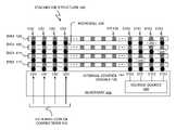
- a memory component employing stacked die structure 400 in accordance with one embodiment of the inventionincludes printed circuit board (“PCB”) substrate 405 , first die (DIE0) 410 , second die (DIE1) 415 , third die (DIE2) 420 and fourth die (DIE3) 425 .
- structure 400utilizes microballs 430 (small solder beads) to interconnect the different die, each of which includes through wafer interconnect vias 435 .
- substrate 405acts to provide structural support and electrical connectivity between the stacked die and the physical package within which stacked die structure 400 is placed.
- Illustrative PCB substrate materialsinclude, but are not limited to, FR2, FR4 and plastics such as Rogers® 4000, Rogers® Duroid, DuPont® Teflon® (types GT and GX), polyimide, polystyrene and cross-linked polystyrene. It will further be recognized that inter-die connections may be made using technologies other than through wafer interconnects and microballs—e.g., wire bonds, flip-chips or combinations of these and other technologies. In addition, it may be desirable or necessary (depending upon the types of die and substrate used) to include a spacer or bonding layer (e.g., epoxy) between each die.
- a spacer or bonding layere.g., epoxy
- external control connections 110convey CHIP SELECT 0 (CS 0 ), CHIP SELECT 1 (CS 1 ), CHIP SELECT 2 (CS 2 ) and CHIP SELECT 3 (CS 3 ) signals.
- internal control signals 120comprise STACK ENABLE 0 (STE 0 ), STACK ENABLE 1 (STE 1 ), STACK ENABLE 2 (STE 2 ) and STACK ENABLE 3 (STE 3 ) signals.
- each of the stack enable connections STEO-STE 3 on PCB substrate 405are electrically coupled to voltage source 440 .
- each die's internal control signal's connection padso that it is biased to a weak ground potential, permits internal control signal inter-die connection patterns (e.g., mircroballs and non-connections 445 , 450 and 455 ) to provide a unique collection of input signals to each decode circuit on each die and, as a consequence, permits the unique selection of die in accordance with external control connections 110 .
- internal control signal inter-die connection patternse.g., mircroballs and non-connections 445 , 450 and 455
- Table 1describes the functional operation of decode circuit 125 .
- the “logic” expressed in Table 1is sufficient to define the operation of decode circuit 125 in accordance with the invention. Having said this, it will also be readily apparent to one of ordinary skill in the art that the illustrated logic is not the only logic possible.
- any pattern of inter-die connectivity that provides a unique set of internal control inputs 120 to each die's decode circuit 125can be used—Table 1 represents but one possible pattern.
- Benefits of the inventioninclude the ability to use any die manufactured in accordance with the invention in any position in a stacked die structure.
- each die's decode circuitcan uniquely select, activate or enable its associated functional circuit.
- stacked die structure components in accordance with the inventioncan be assembled from die manufactured in a consistent manner—since all die for use in a specified stacked die component are the same, no special processing (e.g., formation of redistribution layers) or additional tracking of unique parts are needed during manufacture time. This, in turn, reduces the cost to manufacture such components and improves the overall yield through the elimination of processing steps. (It will be recognized that the amount of circuitry needed to implement decode circuit 125 is de minimus compared to the amount of circuitry (e.g., number of transistors) required to implement functional circuitry 105 .
- stacked die structures in accordance with the inventionare not limited to the illustrative four die component of FIG. 4 .
- components employing a stacked die in accordance with the inventionare not limited to utilizing a single group of external control signals as illustrated in FIG. 4 .
- each die in an SDRAM stacked die component in accordance with the inventionmay selectively pass both CHIP SELECT and CLOCK ENABLE signals to their respective functional circuit (e.g., see FIG. 3 ).
- Other combinations of control signals for die embodying different functional circuitswill be readily apparent to those of ordinary skill in the art.
- stacked die structures in accordance with the inventionare not limited to memory components or, even, the use of die having the same functional circuits (e.g., element 105 in FIG. 1 ).
- die having different functional circuitsare fabricated to include decode circuit and internal control signals in the manner described herein, die with different functional circuits may be used to assemble stacked die components in accordance with the invention.
Landscapes
- Engineering & Computer Science (AREA)
- Microelectronics & Electronic Packaging (AREA)
- Semiconductor Integrated Circuits (AREA)
- Design And Manufacture Of Integrated Circuits (AREA)
Abstract
Description
- This application is a continuation of U.S. patent application Ser. No. 12/013,205, filed Jan. 11, 2008, which was in turn a continuation of U.S. patent application Ser. No. 11/215,648, filed Aug. 30, 2005 (now U.S. Pat No. 7,327,592). Priority is claimed to both of these applications, and both are incorporated herein by reference.
- The invention relates generally to semiconductor devices and, more particularly, to stacked die semiconductor devices and to methods for uniquely identifying individual die within a stacked die structure.
- Semiconductor devices are generally constructed from silicon or gallium arsenide wafers through a fabrication process that involves a number of deposition, masking, diffusion, etching, and implanting steps. Each fabrication run results in a wafer with a number of identical integrated circuit (“IC”) devices formed therein. After fabrication, the wafer is separated into individual units or die, where each die includes one IC device. Traditionally, individual die are encased in a molding and electrically connected to leads that protrude therefrom. More recently, multiple die have been arranged within a single enclosure. In one such arrangement, two or more die are aligned vertically and electrically interconnected to form a single component. Components formed in this manner are said to employ stacked die or a stacked die structure.
- Stacked die structures permit design engineers to increase a system's circuit density - the amount of circuitry per unit area of printed circuit board. Within a stacked die structure, however, it can be important that die are individually selectable. For example, when multiple memory circuit die are stacked to form a single memory component, it can be important that each die be individually activated or selected. In the past, this capability has been provided by remapping various control pins such as chip select and/or clock enable pins from each die within a stack through the use of fuses, anti-fuses and redistribution layers (“RDL”). While these approaches have proven successful, they require that die destined for a first position (e.g., the bottom-most die in a stack) be processed differently from a die destined for a second position (e.g., the top-most die in a stack). In addition to the added cost of processing die in this manner, each die that is different from another die must be segregated and tracked uniquely via a manufacturing parts tracking system, further adding to the cost of conventional stacked die devices. Thus, it would be beneficial to provide improved stacked die structures that utilize dies fabricated in a consistent manner and wherein such die would be capable of automatically sensing their position in a stacked die structure such that they are individually and uniquely selectable.
- The invention provides a semiconductor die having a functional circuit and a decode circuit suitable for use in a stacked die semiconductor component. The decode circuit permits individual die in a stacked die structure to determine their location or position in the stack and, in response, selectively pass one or more external control signals to the decode circuit's associated functional circuit based on inter-die connection patterns. Accordingly, stacked semiconductor die components may be assembled using consistently processed or fabricated semiconductor dies in accordance with the invention.
- In one embodiment, a semiconductor die in accordance with the invention comprises a functional circuit having an enable input connection, a plurality of external control signal connections for receipt of control signals external to the die's package, a plurality of internal control signal input connections and a decode circuit. The decode circuit, in turn, comprises a first set of inputs coupled to the external control signal input connections, a second set of inputs coupled to the internal control signal input connections and an output coupled to the functional circuit's enable input connection. The decode circuit is configured to selectively route a signal coupled to the external control signal input connections to the decoder's output (and, therefore, the functional circuit's enable input connection) based on signals provided by the internal control signal input connections—the state of which is determined by the pattern of inter-die connections.
- In another embodiment, a plurality of known good die in accordance with the invention are vertically stacked and electrically coupled to provide a component having a specified functionality. An illustrative functional circuit comprises a memory array, an illustrative stacked die component comprises a random access memory component and illustrative external control signals comprise chip select and clock enable signals.
FIG. 1 shows, in block diagram form, a semiconductor die in accordance with one embodiment of the invention.FIG. 2 shows, in block diagram form, the decode circuit ofFIG. 1 in accordance with one embodiment of the invention.FIG. 3 shows, in block diagram form, the decode circuit ofFIG. 1 in accordance with another embodiment of the invention.FIG. 4 shows, in block diagram form, a stacked die component in accordance with one embodiment of the invention.- Stacked die structures comprised of consistently fabricated die that automatically sense their position in the structure and are uniquely selectable through specified control signals are described. The following descriptions are presented to enable any person skilled in the art of semiconductor device design and fabrication to make and use the invention as claimed and are provided in the context of the particular examples discussed below, variations of which will be readily apparent to those skilled in the art. Accordingly, the claims appended hereto are not intended to be limited by the disclosed embodiments, but are to be accorded their widest scope consistent with the principles and features disclosed herein.
- In accordance with the invention, a plurality of known good die are stacked and electrically coupled to provide a component having a specified functionality, wherein a plurality of external control pins are provided that permit the unique selection/activation of individual die within the stacked die structure. In a preferred implementation, four functionally identical and consistently manufactured memory die are stacked and interconnected. One type of exemplary memory device is a Synchronous Dynamic Random Access Memory (“SDRAM”) device, such as SDRAM devices designed and manufactured by the Assignee of this document. It is to be understood, however, that this constitutes but one exemplary type of integrated circuit component that can be used in accordance with the inventive concept. Other types of integrated circuit devices (and not necessarily memory devices) can be provided without departing from the spirit and scope of the claimed subject matter.
- Referring to
FIG. 1 , die100 in accordance with one embodiment of the invention comprisesfunctional circuit 105 havingexternal control connections 110 and dieconnections 115. For example,functional circuit 105 could implement a static, dynamic or flash memory array,external control connections 110 could include chip select and/or clock enable inputs and dieconnections 115 could include power, ground, address and data signals as well as other control signals and die testing connections.Internal control signals 120 represent signal paths that are used in accordance with the invention to supplydecode circuit 125. As used herein, “internal control signals” are signals that arise from, and are used by, circuitry inside the target component—that is, from individual die within the component.Decode circuit 125, in turn, controls which one(s) ofexternal control signals 110 are supplied to die control connections130 (e.g., chip select and/or clock enable connections) forfunctional circuit 105. - In general, each die (e.g., die100) for use in a specified stacked die structure component (e.g., a memory component) in accordance with the invention can be manufactured having the same internal
control signal paths 120,decode circuitry 125 and connections betweenexternal control signals 110,decode circuit 125 and diecontrol connections 130. During component fabrication, the pattern of connections betweeninternal control signals 120 on a first die in a stack and its adjacent die(s) determine the input to decodecircuit 125 on each die. In this way, and as well be described in detail below, decodecircuit 125 uniquely conveys one or more signals input viaexternal control connections 110 tofunctional circuit 105 depending upon the die's position in the stack structure. - Referring to
FIG. 2 ,decode circuit 125 comprisesdecoder 200 andselector 205. In practice,decoder 200 “decodes” the pattern of its input signals (internal control signals120) so as to causeselector 205 to pass one of its input signals (provided via external control connections110) to its functional circuit (e.g., circuit105) via diecontrol connection 130. In one embodiment, there are as many external control signals as there are die in the stacked die structure. In a stacked die memory component, for example,external control connections 110 could convey one CHIP SELECT signal for each die in the stacked die structure. In this embodiment, diecontrol connection 130 would provide a single CHIP SELECT signal. In another embodiment, there is a group of external control connections for each unique control signal that is to be provided tofunctional circuit 105. Referring toFIG. 3 , for example, in a stacked die memory componentexternal control connections 110 could convey a first group of CHIP SELECTsignals 300 and a second group of CLOCKENABLE signals 305. Each group of external control signals can drive its own selector,310 and315 respectively. Each selector, in turn, supplies a single output signal (CHIPSELECT signal 320 and CLOCK ENABLE signal325), the collection of which are carried tofunctional circuit 105 viadie control connections 130. - With respect to the described embodiments, it will be recognized that
selectors - To facilitate the use of consistently processed die in accordance with the invention, it will be recognized that each die should have its internal control signals coupled during the die fabrication process in such a manner as to provide an initial value to the die's
decoder circuit 125 when incorporated into a stacked die structure. In many semiconductor device environments, it is common to bias a die's connection pads to a weak ground potential. (By “weak,” it is meant that the value may be readily over-ridden by a voltage level above the die's ground potential.) Using this feature, each internal control signal on a die manufactured in accordance with the invention may be individually coupled to a weak ground potential. When this is done, the final input to each die'sdecoder 200 can be set, determined or specified by the manner in which the die are interconnected at component fabrication time (see discussion below). This, in turn, permits each die'sdecode circuit 125 to uniquely select or enable itsfunctional circuit 105 regardless of its position in the stacked die structure. That is, die in accordance with the invention automatically determine their location within a stacked die structure and activate, enable or select their functional circuitry based upon that location. Accordingly, stacked die components in accordance with the invention do not require that their constituent die be processed to include unique signal remapping features through, for example, extra semiconductor processing steps or post-processing operations such as the formation of redistribution layers. - Consider, by way of example,
FIG. 4 in which a memory component employing stackeddie structure 400 in accordance with one embodiment of the invention includes printed circuit board (“PCB”)substrate 405, first die (DIE0)410, second die (DIE1)415, third die (DIE2)420 and fourth die (DIE3)425. In this embodiment,structure 400 utilizes microballs430 (small solder beads) to interconnect the different die, each of which includes throughwafer interconnect vias 435. It will be recognized thatsubstrate 405 acts to provide structural support and electrical connectivity between the stacked die and the physical package within which stackeddie structure 400 is placed. Illustrative PCB substrate materials include, but are not limited to, FR2, FR4 and plastics such as Rogers® 4000, Rogers® Duroid, DuPont® Teflon® (types GT and GX), polyimide, polystyrene and cross-linked polystyrene. It will further be recognized that inter-die connections may be made using technologies other than through wafer interconnects and microballs—e.g., wire bonds, flip-chips or combinations of these and other technologies. In addition, it may be desirable or necessary (depending upon the types of die and substrate used) to include a spacer or bonding layer (e.g., epoxy) between each die. - As illustrated,
external control connections 110 convey CHIP SELECT0 (CS0), CHIP SELECT1 (CS1), CHIP SELECT2 (CS2) and CHIP SELECT3 (CS3) signals. Similarly, internal control signals120 comprise STACK ENABLE0 (STE0), STACK ENABLE1 (STE1), STACK ENABLE2 (STE2) and STACK ENABLE3 (STE3) signals. As shown, each of the stack enable connections STEO-STE3 onPCB substrate 405 are electrically coupled tovoltage source 440. When this is done in conjunction with connecting (during the die manufacturing process) each die's internal control signal's connection pad so that it is biased to a weak ground potential, permits internal control signal inter-die connection patterns (e.g., mircroballs andnon-connections external control connections 110. - Given the illustrative inter-die connection pattern of
FIG. 4 , Table 1 describes the functional operation ofdecode circuit 125. One of ordinary skill in the art will understand that the “logic” expressed in Table 1 is sufficient to define the operation ofdecode circuit 125 in accordance with the invention. Having said this, it will also be readily apparent to one of ordinary skill in the art that the illustrated logic is not the only logic possible. In accordance with the invention, any pattern of inter-die connectivity that provides a unique set ofinternal control inputs 120 to each die'sdecode circuit 125 can be used—Table 1 represents but one possible pattern. TABLE 1 Illustrative Decode Circuit Function STE0 STE1 STE2 STE3 Die Selected 1 1 1 1 DIE0 1 0 1 1 DIE1 1 0 1 0 DIE2 1 0 0 0 DIE3 - Benefits of the invention include the ability to use any die manufactured in accordance with the invention in any position in a stacked die structure. By selectively interconnecting internal control signal paths between the die in a stack, each die's decode circuit can uniquely select, activate or enable its associated functional circuit. Accordingly, stacked die structure components in accordance with the invention can be assembled from die manufactured in a consistent manner—since all die for use in a specified stacked die component are the same, no special processing (e.g., formation of redistribution layers) or additional tracking of unique parts are needed during manufacture time. This, in turn, reduces the cost to manufacture such components and improves the overall yield through the elimination of processing steps. (It will be recognized that the amount of circuitry needed to implement
decode circuit 125 is de minimus compared to the amount of circuitry (e.g., number of transistors) required to implementfunctional circuitry 105. - Various changes in the materials, components and circuit elements of the illustrated embodiments are possible without departing from the scope of the following claims. For instance, stacked die structures in accordance with the invention are not limited to the illustrative four die component of
FIG. 4 . Similarly, components employing a stacked die in accordance with the invention are not limited to utilizing a single group of external control signals as illustrated inFIG. 4 . For example, each die in an SDRAM stacked die component in accordance with the invention may selectively pass both CHIP SELECT and CLOCK ENABLE signals to their respective functional circuit (e.g., seeFIG. 3 ). Other combinations of control signals for die embodying different functional circuits will be readily apparent to those of ordinary skill in the art. In addition, stacked die structures in accordance with the invention are not limited to memory components or, even, the use of die having the same functional circuits (e.g.,element 105 inFIG. 1 ). As long as die having different functional circuits are fabricated to include decode circuit and internal control signals in the manner described herein, die with different functional circuits may be used to assemble stacked die components in accordance with the invention.
Claims (28)
Priority Applications (2)
| Application Number | Priority Date | Filing Date | Title |
|---|---|---|---|
| US12/535,092US8144497B2 (en) | 2005-08-30 | 2009-08-04 | Self-identifying stacked die semiconductor components |
| US13/419,171US8472232B2 (en) | 2005-08-30 | 2012-03-13 | Self-identifying stacked die semiconductor components |
Applications Claiming Priority (3)
| Application Number | Priority Date | Filing Date | Title |
|---|---|---|---|
| US11/215,648US7327592B2 (en) | 2005-08-30 | 2005-08-30 | Self-identifying stacked die semiconductor components |
| US12/013,205US7573733B2 (en) | 2005-08-30 | 2008-01-11 | Self-identifying stacked die semiconductor components |
| US12/535,092US8144497B2 (en) | 2005-08-30 | 2009-08-04 | Self-identifying stacked die semiconductor components |
Related Parent Applications (1)
| Application Number | Title | Priority Date | Filing Date |
|---|---|---|---|
| US12/013,205ContinuationUS7573733B2 (en) | 2005-08-30 | 2008-01-11 | Self-identifying stacked die semiconductor components |
Related Child Applications (1)
| Application Number | Title | Priority Date | Filing Date |
|---|---|---|---|
| US13/419,171ContinuationUS8472232B2 (en) | 2005-08-30 | 2012-03-13 | Self-identifying stacked die semiconductor components |
Publications (2)
| Publication Number | Publication Date |
|---|---|
| US20090289701A1true US20090289701A1 (en) | 2009-11-26 |
| US8144497B2 US8144497B2 (en) | 2012-03-27 |
Family
ID=37803827
Family Applications (4)
| Application Number | Title | Priority Date | Filing Date |
|---|---|---|---|
| US11/215,648Active2025-10-20US7327592B2 (en) | 2005-08-30 | 2005-08-30 | Self-identifying stacked die semiconductor components |
| US12/013,205Expired - LifetimeUS7573733B2 (en) | 2005-08-30 | 2008-01-11 | Self-identifying stacked die semiconductor components |
| US12/535,092Active2026-02-25US8144497B2 (en) | 2005-08-30 | 2009-08-04 | Self-identifying stacked die semiconductor components |
| US13/419,171Expired - LifetimeUS8472232B2 (en) | 2005-08-30 | 2012-03-13 | Self-identifying stacked die semiconductor components |
Family Applications Before (2)
| Application Number | Title | Priority Date | Filing Date |
|---|---|---|---|
| US11/215,648Active2025-10-20US7327592B2 (en) | 2005-08-30 | 2005-08-30 | Self-identifying stacked die semiconductor components |
| US12/013,205Expired - LifetimeUS7573733B2 (en) | 2005-08-30 | 2008-01-11 | Self-identifying stacked die semiconductor components |
Family Applications After (1)
| Application Number | Title | Priority Date | Filing Date |
|---|---|---|---|
| US13/419,171Expired - LifetimeUS8472232B2 (en) | 2005-08-30 | 2012-03-13 | Self-identifying stacked die semiconductor components |
Country Status (7)
| Country | Link |
|---|---|
| US (4) | US7327592B2 (en) |
| EP (1) | EP1932156B1 (en) |
| JP (1) | JP2009506476A (en) |
| KR (1) | KR100931760B1 (en) |
| CN (1) | CN101253568B (en) |
| TW (1) | TWI309420B (en) |
| WO (1) | WO2007027376A1 (en) |
Cited By (3)
| Publication number | Priority date | Publication date | Assignee | Title |
|---|---|---|---|---|
| US20120049361A1 (en)* | 2010-08-27 | 2012-03-01 | Byoung-Kwon Park | Semiconductor integrated circuit |
| KR101179268B1 (en) | 2010-08-05 | 2012-09-03 | 에스케이하이닉스 주식회사 | Semiconductor package with chip selection by through-vias |
| WO2014018772A1 (en)* | 2012-07-26 | 2014-01-30 | Micron Technology, Inc. | Device identification assignment and total device number detection |
Families Citing this family (41)
| Publication number | Priority date | Publication date | Assignee | Title |
|---|---|---|---|---|
| KR101377305B1 (en)* | 2005-06-24 | 2014-03-25 | 구글 인코포레이티드 | An integrated memory core and memory interface circuit |
| US7327592B2 (en)* | 2005-08-30 | 2008-02-05 | Micron Technology, Inc. | Self-identifying stacked die semiconductor components |
| US7352602B2 (en)* | 2005-12-30 | 2008-04-01 | Micron Technology, Inc. | Configurable inputs and outputs for memory stacking system and method |
| KR100832845B1 (en)* | 2006-10-03 | 2008-05-28 | 삼성전자주식회사 | Semiconductor package structure and manufacturing method thereof |
| JP5616636B2 (en) | 2006-12-14 | 2014-10-29 | ラムバス・インコーポレーテッド | Multi-die memory device |
| US20090043917A1 (en)* | 2007-08-06 | 2009-02-12 | Thilo Wagner | Electronic Circuit and Method for Selecting an Electronic Circuit |
| CN101803237B (en)* | 2007-09-13 | 2013-07-10 | Lg电子株式会社 | Method for allocating wireless resources in wireless communication system |
| US7760533B2 (en)* | 2007-10-02 | 2010-07-20 | Micron Technology, Inc. | Systems, methods and devices for arbitrating die stack position in a multi-bit stack device |
| JP2009129498A (en)* | 2007-11-22 | 2009-06-11 | Toshiba Corp | Semiconductor memory device |
| US8130527B2 (en) | 2008-09-11 | 2012-03-06 | Micron Technology, Inc. | Stacked device identification assignment |
| US20100121994A1 (en)* | 2008-11-10 | 2010-05-13 | International Business Machines Corporation | Stacked memory array |
| US8032804B2 (en)* | 2009-01-12 | 2011-10-04 | Micron Technology, Inc. | Systems and methods for monitoring a memory system |
| JP5632584B2 (en) | 2009-02-05 | 2014-11-26 | ピーエスフォー ルクスコ エスエイアールエルPS4 Luxco S.a.r.l. | Semiconductor device |
| US8018752B2 (en) | 2009-03-23 | 2011-09-13 | Micron Technology, Inc. | Configurable bandwidth memory devices and methods |
| TWI474331B (en)* | 2009-06-30 | 2015-02-21 | Hitachi Ltd | Semiconductor device |
| US8328218B2 (en)* | 2009-07-13 | 2012-12-11 | Columbia Cycle Works, LLC | Commuter vehicle |
| US8063654B2 (en)* | 2009-07-17 | 2011-11-22 | Xilinx, Inc. | Apparatus and method for testing of stacked die structure |
| CN102598255A (en) | 2009-10-23 | 2012-07-18 | 拉姆伯斯公司 | Stacked semiconductor device |
| TWI442401B (en)* | 2009-12-30 | 2014-06-21 | Macronix Int Co Ltd | 3d chip select for sheard input packages |
| US8612809B2 (en)* | 2009-12-31 | 2013-12-17 | Intel Corporation | Systems, methods, and apparatuses for stacked memory |
| US8327225B2 (en)* | 2010-01-04 | 2012-12-04 | Micron Technology, Inc. | Error correction in a stacked memory |
| WO2011115648A1 (en) | 2010-03-15 | 2011-09-22 | Rambus Inc. | Chip selection in a symmetric interconnection topology |
| WO2013006187A1 (en)* | 2011-07-05 | 2013-01-10 | Intel Corporation | Self-disabling chip enable input |
| US8476771B2 (en) | 2011-08-25 | 2013-07-02 | International Business Machines Corporation | Configuration of connections in a 3D stack of integrated circuits |
| US8516426B2 (en) | 2011-08-25 | 2013-08-20 | International Business Machines Corporation | Vertical power budgeting and shifting for three-dimensional integration |
| US8381156B1 (en) | 2011-08-25 | 2013-02-19 | International Business Machines Corporation | 3D inter-stratum connectivity robustness |
| US8519735B2 (en) | 2011-08-25 | 2013-08-27 | International Business Machines Corporation | Programming the behavior of individual chips or strata in a 3D stack of integrated circuits |
| US8525569B2 (en) | 2011-08-25 | 2013-09-03 | International Business Machines Corporation | Synchronizing global clocks in 3D stacks of integrated circuits by shorting the clock network |
| US8476953B2 (en) | 2011-08-25 | 2013-07-02 | International Business Machines Corporation | 3D integrated circuit stack-wide synchronization circuit |
| US8587357B2 (en) | 2011-08-25 | 2013-11-19 | International Business Machines Corporation | AC supply noise reduction in a 3D stack with voltage sensing and clock shifting |
| US8576000B2 (en) | 2011-08-25 | 2013-11-05 | International Business Machines Corporation | 3D chip stack skew reduction with resonant clock and inductive coupling |
| CN103426452B (en)* | 2012-05-16 | 2016-03-02 | 北京兆易创新科技股份有限公司 | A kind of storer cascade and method for packing and device thereof |
| CN103678164B (en)* | 2012-09-25 | 2016-12-21 | 北京兆易创新科技股份有限公司 | A kind of storage level linked method and device |
| US9194912B2 (en) | 2012-11-29 | 2015-11-24 | International Business Machines Corporation | Circuits for self-reconfiguration or intrinsic functional changes of chips before vs. after stacking |
| KR102092745B1 (en)* | 2013-10-24 | 2020-03-24 | 에스케이하이닉스 주식회사 | Semiconductor appratus and testing method thereof |
| US9559113B2 (en) | 2014-05-01 | 2017-01-31 | Macronix International Co., Ltd. | SSL/GSL gate oxide in 3D vertical channel NAND |
| US10002653B2 (en) | 2014-10-28 | 2018-06-19 | Nxp Usa, Inc. | Die stack address bus having a programmable width |
| US10283171B2 (en)* | 2015-03-30 | 2019-05-07 | Taiwan Semicondutor Manufacturing Company, Ltd. | Stacked die semiconductor device with separate bit line and bit line bar interconnect structures |
| CN112599528B (en)* | 2020-12-14 | 2022-07-12 | 武汉新芯集成电路制造有限公司 | Semiconductor device and method for manufacturing the same |
| US12112792B2 (en)* | 2021-08-10 | 2024-10-08 | Micron Technology, Inc. | Memory device for wafer-on-wafer formed memory and logic |
| CN114822635A (en)* | 2022-06-28 | 2022-07-29 | 浙江力积存储科技有限公司 | Chip position identification method and chip time sequence setting method based on same |
Citations (14)
| Publication number | Priority date | Publication date | Assignee | Title |
|---|---|---|---|---|
| US5173766A (en)* | 1990-06-25 | 1992-12-22 | Lsi Logic Corporation | Semiconductor device package and method of making such a package |
| US5291061A (en)* | 1993-04-06 | 1994-03-01 | Micron Semiconductor, Inc. | Multi-chip stacked devices |
| US6168973B1 (en)* | 1998-08-28 | 2001-01-02 | Medtronic, Inc. | Semiconductor stacked device for implantable medical apparatus and method for making same |
| US6218895B1 (en)* | 1997-06-20 | 2001-04-17 | Intel Corporation | Multiple well transistor circuits having forward body bias |
| US6400008B1 (en)* | 1996-02-16 | 2002-06-04 | Micron Technology, Inc. | Surface mount ic using silicon vias in an area array format or same size as die array |
| US6417695B1 (en)* | 2001-03-15 | 2002-07-09 | Micron Technology, Inc. | Antifuse reroute of dies |
| US6696318B2 (en)* | 2000-12-11 | 2004-02-24 | Medtronic, Inc. | Methods for forming a die package |
| US6706557B2 (en)* | 2001-09-21 | 2004-03-16 | Micron Technology, Inc. | Method of fabricating stacked die configurations utilizing redistribution bond pads |
| US6713193B2 (en)* | 2002-05-14 | 2004-03-30 | Lightronik Technology Inc. | Organic EL device |
| US20050041453A1 (en)* | 2003-08-22 | 2005-02-24 | Brazis Paul W. | Method and apparatus for reading and writing to solid-state memory |
| US20050162946A1 (en)* | 2004-01-21 | 2005-07-28 | Seiko Epson Corporation | Stacked layered type semiconductor memory device |
| US7046538B2 (en)* | 2004-09-01 | 2006-05-16 | Micron Technology, Inc. | Memory stacking system and method |
| US7200021B2 (en)* | 2004-12-10 | 2007-04-03 | Infineon Technologies Ag | Stacked DRAM memory chip for a dual inline memory module (DIMM) |
| US7379316B2 (en)* | 2005-09-02 | 2008-05-27 | Metaram, Inc. | Methods and apparatus of stacking DRAMs |
Family Cites Families (15)
| Publication number | Priority date | Publication date | Assignee | Title |
|---|---|---|---|---|
| JPS6313497A (en)* | 1986-07-02 | 1988-01-20 | Nec Corp | Underwater wide band frequency transmitter/receiver |
| JPH03295266A (en)* | 1990-04-12 | 1991-12-26 | Hitachi Ltd | Highly integrated semiconductor device |
| JP2799788B2 (en) | 1991-08-28 | 1998-09-21 | 富士写真フイルム株式会社 | Winding core and winding body for rolled photo film |
| JP3563604B2 (en)* | 1998-07-29 | 2004-09-08 | 株式会社東芝 | Multi-chip semiconductor device and memory card |
| US6487102B1 (en)* | 2000-09-18 | 2002-11-26 | Intel Corporation | Memory module having buffer for isolating stacked memory devices |
| JP2003060053A (en)* | 2001-08-10 | 2003-02-28 | Fujitsu Ltd | Semiconductor chip, semiconductor integrated circuit device using the same, and semiconductor chip selection method |
| US6813193B2 (en)* | 2003-04-02 | 2004-11-02 | Infineon Technologies, Ag | Memory device and method of outputting data from a memory device |
| JP4272968B2 (en)* | 2003-10-16 | 2009-06-03 | エルピーダメモリ株式会社 | Semiconductor device and semiconductor chip control method |
| JP4309368B2 (en)* | 2005-03-30 | 2009-08-05 | エルピーダメモリ株式会社 | Semiconductor memory device |
| JP4577688B2 (en)* | 2005-05-09 | 2010-11-10 | エルピーダメモリ株式会社 | Semiconductor chip selection method, semiconductor chip, and semiconductor integrated circuit device |
| US7327592B2 (en)* | 2005-08-30 | 2008-02-05 | Micron Technology, Inc. | Self-identifying stacked die semiconductor components |
| US8120958B2 (en)* | 2007-12-24 | 2012-02-21 | Qimonda Ag | Multi-die memory, apparatus and multi-die memory stack |
| US7701251B1 (en)* | 2008-03-06 | 2010-04-20 | Xilinx, Inc. | Methods and apparatus for implementing a stacked memory programmable integrated circuit system in package |
| US7973555B1 (en)* | 2008-05-28 | 2011-07-05 | Xilinx, Inc. | Configuration interface to stacked FPGA |
| US9160349B2 (en)* | 2009-08-27 | 2015-10-13 | Micron Technology, Inc. | Die location compensation |
- 2005
- 2005-08-30USUS11/215,648patent/US7327592B2/enactiveActive
- 2006
- 2006-08-07KRKR1020087004987Apatent/KR100931760B1/enactiveActive
- 2006-08-07JPJP2008529054Apatent/JP2009506476A/enactivePending
- 2006-08-07WOPCT/US2006/030692patent/WO2007027376A1/enactiveApplication Filing
- 2006-08-07CNCN2006800318361Apatent/CN101253568B/enactiveActive
- 2006-08-07EPEP06800871.3Apatent/EP1932156B1/enactiveActive
- 2006-08-16TWTW095130018Apatent/TWI309420B/enactive
- 2008
- 2008-01-11USUS12/013,205patent/US7573733B2/ennot_activeExpired - Lifetime
- 2009
- 2009-08-04USUS12/535,092patent/US8144497B2/enactiveActive
- 2012
- 2012-03-13USUS13/419,171patent/US8472232B2/ennot_activeExpired - Lifetime
Patent Citations (14)
| Publication number | Priority date | Publication date | Assignee | Title |
|---|---|---|---|---|
| US5173766A (en)* | 1990-06-25 | 1992-12-22 | Lsi Logic Corporation | Semiconductor device package and method of making such a package |
| US5291061A (en)* | 1993-04-06 | 1994-03-01 | Micron Semiconductor, Inc. | Multi-chip stacked devices |
| US6400008B1 (en)* | 1996-02-16 | 2002-06-04 | Micron Technology, Inc. | Surface mount ic using silicon vias in an area array format or same size as die array |
| US6218895B1 (en)* | 1997-06-20 | 2001-04-17 | Intel Corporation | Multiple well transistor circuits having forward body bias |
| US6168973B1 (en)* | 1998-08-28 | 2001-01-02 | Medtronic, Inc. | Semiconductor stacked device for implantable medical apparatus and method for making same |
| US6696318B2 (en)* | 2000-12-11 | 2004-02-24 | Medtronic, Inc. | Methods for forming a die package |
| US6417695B1 (en)* | 2001-03-15 | 2002-07-09 | Micron Technology, Inc. | Antifuse reroute of dies |
| US6706557B2 (en)* | 2001-09-21 | 2004-03-16 | Micron Technology, Inc. | Method of fabricating stacked die configurations utilizing redistribution bond pads |
| US6713193B2 (en)* | 2002-05-14 | 2004-03-30 | Lightronik Technology Inc. | Organic EL device |
| US20050041453A1 (en)* | 2003-08-22 | 2005-02-24 | Brazis Paul W. | Method and apparatus for reading and writing to solid-state memory |
| US20050162946A1 (en)* | 2004-01-21 | 2005-07-28 | Seiko Epson Corporation | Stacked layered type semiconductor memory device |
| US7046538B2 (en)* | 2004-09-01 | 2006-05-16 | Micron Technology, Inc. | Memory stacking system and method |
| US7200021B2 (en)* | 2004-12-10 | 2007-04-03 | Infineon Technologies Ag | Stacked DRAM memory chip for a dual inline memory module (DIMM) |
| US7379316B2 (en)* | 2005-09-02 | 2008-05-27 | Metaram, Inc. | Methods and apparatus of stacking DRAMs |
Cited By (5)
| Publication number | Priority date | Publication date | Assignee | Title |
|---|---|---|---|---|
| KR101179268B1 (en) | 2010-08-05 | 2012-09-03 | 에스케이하이닉스 주식회사 | Semiconductor package with chip selection by through-vias |
| US8624375B2 (en) | 2010-08-05 | 2014-01-07 | SK Hynix Inc. | Semiconductor package for selecting semiconductor chip from a chip stack |
| US20120049361A1 (en)* | 2010-08-27 | 2012-03-01 | Byoung-Kwon Park | Semiconductor integrated circuit |
| WO2014018772A1 (en)* | 2012-07-26 | 2014-01-30 | Micron Technology, Inc. | Device identification assignment and total device number detection |
| US9478502B2 (en) | 2012-07-26 | 2016-10-25 | Micron Technology, Inc. | Device identification assignment and total device number detection |
Also Published As
| Publication number | Publication date |
|---|---|
| WO2007027376A1 (en) | 2007-03-08 |
| US20070047284A1 (en) | 2007-03-01 |
| US8144497B2 (en) | 2012-03-27 |
| JP2009506476A (en) | 2009-02-12 |
| KR20080033478A (en) | 2008-04-16 |
| US7327592B2 (en) | 2008-02-05 |
| EP1932156A4 (en) | 2010-10-27 |
| US7573733B2 (en) | 2009-08-11 |
| EP1932156A1 (en) | 2008-06-18 |
| US20120176192A1 (en) | 2012-07-12 |
| US20080130395A1 (en) | 2008-06-05 |
| KR100931760B1 (en) | 2009-12-14 |
| US8472232B2 (en) | 2013-06-25 |
| CN101253568B (en) | 2010-10-13 |
| CN101253568A (en) | 2008-08-27 |
| EP1932156B1 (en) | 2016-09-21 |
| TWI309420B (en) | 2009-05-01 |
| TW200725636A (en) | 2007-07-01 |
Similar Documents
| Publication | Publication Date | Title |
|---|---|---|
| US8144497B2 (en) | Self-identifying stacked die semiconductor components | |
| US6356958B1 (en) | Integrated circuit module has common function known good integrated circuit die with multiple selectable functions | |
| US8315068B2 (en) | Integrated circuit die stacks having initially identical dies personalized with fuses and methods of manufacturing the same | |
| JP5209927B2 (en) | Manufacturing method of semiconductor structure | |
| KR100438883B1 (en) | Multi chip semiconductor device and memory card | |
| US7046522B2 (en) | Method for scalable architectures in stackable three-dimensional integrated circuits and electronics | |
| US6864122B1 (en) | Multi-chip module having content addressable memory | |
| US20110309518A1 (en) | Semiconductor device with configurable through-silicon vias | |
| JPH0754829B2 (en) | Input circuit for an integrated circuit chip and method for providing multifunction to an input pin of an integrated circuit chip | |
| KR20070056110A (en) | Memory Stacking Systems and Methods | |
| KR20030036028A (en) | 3-d-memory device for large storage capacity | |
| US8625381B2 (en) | Stacked semiconductor device | |
| US6718432B1 (en) | Method and apparatus for transparent cascading of multiple content addressable memory devices | |
| US7131033B1 (en) | Substrate configurable JTAG ID scheme | |
| US6339559B1 (en) | Decode scheme for programming antifuses arranged in banks | |
| CN119855164B (en) | Memory chip, logic chip, chip stacking structure and memory | |
| US7539034B2 (en) | Memory configured on a common substrate | |
| TW201442196A (en) | A stacked chip system | |
| JPH05274866A (en) | Semiconductor device |
Legal Events
| Date | Code | Title | Description |
|---|---|---|---|
| AS | Assignment | Owner name:MICRON TECHNOLOGY, INC., IDAHO Free format text:ASSIGNMENT OF ASSIGNORS INTEREST;ASSIGNOR:SILVESTRI, PAUL;REEL/FRAME:023048/0793 Effective date:20050829 | |
| FEPP | Fee payment procedure | Free format text:PAYOR NUMBER ASSIGNED (ORIGINAL EVENT CODE: ASPN); ENTITY STATUS OF PATENT OWNER: LARGE ENTITY | |
| FEPP | Fee payment procedure | Free format text:PAYER NUMBER DE-ASSIGNED (ORIGINAL EVENT CODE: RMPN); ENTITY STATUS OF PATENT OWNER: LARGE ENTITY Free format text:PAYOR NUMBER ASSIGNED (ORIGINAL EVENT CODE: ASPN); ENTITY STATUS OF PATENT OWNER: LARGE ENTITY | |
| STCF | Information on status: patent grant | Free format text:PATENTED CASE | |
| FPAY | Fee payment | Year of fee payment:4 | |
| AS | Assignment | Owner name:U.S. BANK NATIONAL ASSOCIATION, AS COLLATERAL AGENT, CALIFORNIA Free format text:SECURITY INTEREST;ASSIGNOR:MICRON TECHNOLOGY, INC.;REEL/FRAME:038669/0001 Effective date:20160426 Owner name:U.S. BANK NATIONAL ASSOCIATION, AS COLLATERAL AGEN Free format text:SECURITY INTEREST;ASSIGNOR:MICRON TECHNOLOGY, INC.;REEL/FRAME:038669/0001 Effective date:20160426 | |
| AS | Assignment | Owner name:MORGAN STANLEY SENIOR FUNDING, INC., AS COLLATERAL AGENT, MARYLAND Free format text:PATENT SECURITY AGREEMENT;ASSIGNOR:MICRON TECHNOLOGY, INC.;REEL/FRAME:038954/0001 Effective date:20160426 Owner name:MORGAN STANLEY SENIOR FUNDING, INC., AS COLLATERAL Free format text:PATENT SECURITY AGREEMENT;ASSIGNOR:MICRON TECHNOLOGY, INC.;REEL/FRAME:038954/0001 Effective date:20160426 | |
| AS | Assignment | Owner name:U.S. BANK NATIONAL ASSOCIATION, AS COLLATERAL AGENT, CALIFORNIA Free format text:CORRECTIVE ASSIGNMENT TO CORRECT THE REPLACE ERRONEOUSLY FILED PATENT #7358718 WITH THE CORRECT PATENT #7358178 PREVIOUSLY RECORDED ON REEL 038669 FRAME 0001. ASSIGNOR(S) HEREBY CONFIRMS THE SECURITY INTEREST;ASSIGNOR:MICRON TECHNOLOGY, INC.;REEL/FRAME:043079/0001 Effective date:20160426 Owner name:U.S. BANK NATIONAL ASSOCIATION, AS COLLATERAL AGEN Free format text:CORRECTIVE ASSIGNMENT TO CORRECT THE REPLACE ERRONEOUSLY FILED PATENT #7358718 WITH THE CORRECT PATENT #7358178 PREVIOUSLY RECORDED ON REEL 038669 FRAME 0001. ASSIGNOR(S) HEREBY CONFIRMS THE SECURITY INTEREST;ASSIGNOR:MICRON TECHNOLOGY, INC.;REEL/FRAME:043079/0001 Effective date:20160426 | |
| AS | Assignment | Owner name:JPMORGAN CHASE BANK, N.A., AS COLLATERAL AGENT, ILLINOIS Free format text:SECURITY INTEREST;ASSIGNORS:MICRON TECHNOLOGY, INC.;MICRON SEMICONDUCTOR PRODUCTS, INC.;REEL/FRAME:047540/0001 Effective date:20180703 Owner name:JPMORGAN CHASE BANK, N.A., AS COLLATERAL AGENT, IL Free format text:SECURITY INTEREST;ASSIGNORS:MICRON TECHNOLOGY, INC.;MICRON SEMICONDUCTOR PRODUCTS, INC.;REEL/FRAME:047540/0001 Effective date:20180703 | |
| AS | Assignment | Owner name:MICRON TECHNOLOGY, INC., IDAHO Free format text:RELEASE BY SECURED PARTY;ASSIGNOR:U.S. BANK NATIONAL ASSOCIATION, AS COLLATERAL AGENT;REEL/FRAME:047243/0001 Effective date:20180629 | |
| MAFP | Maintenance fee payment | Free format text:PAYMENT OF MAINTENANCE FEE, 8TH YEAR, LARGE ENTITY (ORIGINAL EVENT CODE: M1552); ENTITY STATUS OF PATENT OWNER: LARGE ENTITY Year of fee payment:8 | |
| AS | Assignment | Owner name:MICRON TECHNOLOGY, INC., IDAHO Free format text:RELEASE BY SECURED PARTY;ASSIGNOR:MORGAN STANLEY SENIOR FUNDING, INC., AS COLLATERAL AGENT;REEL/FRAME:050937/0001 Effective date:20190731 | |
| AS | Assignment | Owner name:MICRON SEMICONDUCTOR PRODUCTS, INC., IDAHO Free format text:RELEASE BY SECURED PARTY;ASSIGNOR:JPMORGAN CHASE BANK, N.A., AS COLLATERAL AGENT;REEL/FRAME:051028/0001 Effective date:20190731 Owner name:MICRON TECHNOLOGY, INC., IDAHO Free format text:RELEASE BY SECURED PARTY;ASSIGNOR:JPMORGAN CHASE BANK, N.A., AS COLLATERAL AGENT;REEL/FRAME:051028/0001 Effective date:20190731 | |
| MAFP | Maintenance fee payment | Free format text:PAYMENT OF MAINTENANCE FEE, 12TH YEAR, LARGE ENTITY (ORIGINAL EVENT CODE: M1553); ENTITY STATUS OF PATENT OWNER: LARGE ENTITY Year of fee payment:12 |