US20090280650A1 - Flowable dielectric equipment and processes - Google Patents
Flowable dielectric equipment and processesDownload PDFInfo
- Publication number
- US20090280650A1 US20090280650A1US12/210,982US21098208AUS2009280650A1US 20090280650 A1US20090280650 A1US 20090280650A1US 21098208 AUS21098208 AUS 21098208AUS 2009280650 A1US2009280650 A1US 2009280650A1
- Authority
- US
- United States
- Prior art keywords
- plasma
- plasma region
- substrate
- region
- gas
- Prior art date
- Legal status (The legal status is an assumption and is not a legal conclusion. Google has not performed a legal analysis and makes no representation as to the accuracy of the status listed.)
- Granted
Links
Images


Classifications
- B—PERFORMING OPERATIONS; TRANSPORTING
- B08—CLEANING
- B08B—CLEANING IN GENERAL; PREVENTION OF FOULING IN GENERAL
- B08B7/00—Cleaning by methods not provided for in a single other subclass or a single group in this subclass
- C—CHEMISTRY; METALLURGY
- C23—COATING METALLIC MATERIAL; COATING MATERIAL WITH METALLIC MATERIAL; CHEMICAL SURFACE TREATMENT; DIFFUSION TREATMENT OF METALLIC MATERIAL; COATING BY VACUUM EVAPORATION, BY SPUTTERING, BY ION IMPLANTATION OR BY CHEMICAL VAPOUR DEPOSITION, IN GENERAL; INHIBITING CORROSION OF METALLIC MATERIAL OR INCRUSTATION IN GENERAL
- C23C—COATING METALLIC MATERIAL; COATING MATERIAL WITH METALLIC MATERIAL; SURFACE TREATMENT OF METALLIC MATERIAL BY DIFFUSION INTO THE SURFACE, BY CHEMICAL CONVERSION OR SUBSTITUTION; COATING BY VACUUM EVAPORATION, BY SPUTTERING, BY ION IMPLANTATION OR BY CHEMICAL VAPOUR DEPOSITION, IN GENERAL
- C23C16/00—Chemical coating by decomposition of gaseous compounds, without leaving reaction products of surface material in the coating, i.e. chemical vapour deposition [CVD] processes
- C23C16/44—Chemical coating by decomposition of gaseous compounds, without leaving reaction products of surface material in the coating, i.e. chemical vapour deposition [CVD] processes characterised by the method of coating
- C23C16/4401—Means for minimising impurities, e.g. dust, moisture or residual gas, in the reaction chamber
- C23C16/4405—Cleaning of reactor or parts inside the reactor by using reactive gases
- C—CHEMISTRY; METALLURGY
- C23—COATING METALLIC MATERIAL; COATING MATERIAL WITH METALLIC MATERIAL; CHEMICAL SURFACE TREATMENT; DIFFUSION TREATMENT OF METALLIC MATERIAL; COATING BY VACUUM EVAPORATION, BY SPUTTERING, BY ION IMPLANTATION OR BY CHEMICAL VAPOUR DEPOSITION, IN GENERAL; INHIBITING CORROSION OF METALLIC MATERIAL OR INCRUSTATION IN GENERAL
- C23C—COATING METALLIC MATERIAL; COATING MATERIAL WITH METALLIC MATERIAL; SURFACE TREATMENT OF METALLIC MATERIAL BY DIFFUSION INTO THE SURFACE, BY CHEMICAL CONVERSION OR SUBSTITUTION; COATING BY VACUUM EVAPORATION, BY SPUTTERING, BY ION IMPLANTATION OR BY CHEMICAL VAPOUR DEPOSITION, IN GENERAL
- C23C16/00—Chemical coating by decomposition of gaseous compounds, without leaving reaction products of surface material in the coating, i.e. chemical vapour deposition [CVD] processes
- C23C16/44—Chemical coating by decomposition of gaseous compounds, without leaving reaction products of surface material in the coating, i.e. chemical vapour deposition [CVD] processes characterised by the method of coating
- C23C16/448—Chemical coating by decomposition of gaseous compounds, without leaving reaction products of surface material in the coating, i.e. chemical vapour deposition [CVD] processes characterised by the method of coating characterised by the method used for generating reactive gas streams, e.g. by evaporation or sublimation of precursor materials
- C23C16/452—Chemical coating by decomposition of gaseous compounds, without leaving reaction products of surface material in the coating, i.e. chemical vapour deposition [CVD] processes characterised by the method of coating characterised by the method used for generating reactive gas streams, e.g. by evaporation or sublimation of precursor materials by activating reactive gas streams before their introduction into the reaction chamber, e.g. by ionisation or addition of reactive species
- C—CHEMISTRY; METALLURGY
- C23—COATING METALLIC MATERIAL; COATING MATERIAL WITH METALLIC MATERIAL; CHEMICAL SURFACE TREATMENT; DIFFUSION TREATMENT OF METALLIC MATERIAL; COATING BY VACUUM EVAPORATION, BY SPUTTERING, BY ION IMPLANTATION OR BY CHEMICAL VAPOUR DEPOSITION, IN GENERAL; INHIBITING CORROSION OF METALLIC MATERIAL OR INCRUSTATION IN GENERAL
- C23C—COATING METALLIC MATERIAL; COATING MATERIAL WITH METALLIC MATERIAL; SURFACE TREATMENT OF METALLIC MATERIAL BY DIFFUSION INTO THE SURFACE, BY CHEMICAL CONVERSION OR SUBSTITUTION; COATING BY VACUUM EVAPORATION, BY SPUTTERING, BY ION IMPLANTATION OR BY CHEMICAL VAPOUR DEPOSITION, IN GENERAL
- C23C16/00—Chemical coating by decomposition of gaseous compounds, without leaving reaction products of surface material in the coating, i.e. chemical vapour deposition [CVD] processes
- C23C16/44—Chemical coating by decomposition of gaseous compounds, without leaving reaction products of surface material in the coating, i.e. chemical vapour deposition [CVD] processes characterised by the method of coating
- C23C16/455—Chemical coating by decomposition of gaseous compounds, without leaving reaction products of surface material in the coating, i.e. chemical vapour deposition [CVD] processes characterised by the method of coating characterised by the method used for introducing gases into reaction chamber or for modifying gas flows in reaction chamber
- C23C16/45514—Mixing in close vicinity to the substrate
- C—CHEMISTRY; METALLURGY
- C23—COATING METALLIC MATERIAL; COATING MATERIAL WITH METALLIC MATERIAL; CHEMICAL SURFACE TREATMENT; DIFFUSION TREATMENT OF METALLIC MATERIAL; COATING BY VACUUM EVAPORATION, BY SPUTTERING, BY ION IMPLANTATION OR BY CHEMICAL VAPOUR DEPOSITION, IN GENERAL; INHIBITING CORROSION OF METALLIC MATERIAL OR INCRUSTATION IN GENERAL
- C23C—COATING METALLIC MATERIAL; COATING MATERIAL WITH METALLIC MATERIAL; SURFACE TREATMENT OF METALLIC MATERIAL BY DIFFUSION INTO THE SURFACE, BY CHEMICAL CONVERSION OR SUBSTITUTION; COATING BY VACUUM EVAPORATION, BY SPUTTERING, BY ION IMPLANTATION OR BY CHEMICAL VAPOUR DEPOSITION, IN GENERAL
- C23C16/00—Chemical coating by decomposition of gaseous compounds, without leaving reaction products of surface material in the coating, i.e. chemical vapour deposition [CVD] processes
- C23C16/44—Chemical coating by decomposition of gaseous compounds, without leaving reaction products of surface material in the coating, i.e. chemical vapour deposition [CVD] processes characterised by the method of coating
- C23C16/50—Chemical coating by decomposition of gaseous compounds, without leaving reaction products of surface material in the coating, i.e. chemical vapour deposition [CVD] processes characterised by the method of coating using electric discharges
- C23C16/505—Chemical coating by decomposition of gaseous compounds, without leaving reaction products of surface material in the coating, i.e. chemical vapour deposition [CVD] processes characterised by the method of coating using electric discharges using radio frequency discharges
- C23C16/509—Chemical coating by decomposition of gaseous compounds, without leaving reaction products of surface material in the coating, i.e. chemical vapour deposition [CVD] processes characterised by the method of coating using electric discharges using radio frequency discharges using internal electrodes
- H—ELECTRICITY
- H01—ELECTRIC ELEMENTS
- H01J—ELECTRIC DISCHARGE TUBES OR DISCHARGE LAMPS
- H01J37/00—Discharge tubes with provision for introducing objects or material to be exposed to the discharge, e.g. for the purpose of examination or processing thereof
- H01J37/32—Gas-filled discharge tubes
- H01J37/32431—Constructional details of the reactor
- H01J37/3244—Gas supply means
- H01J37/32449—Gas control, e.g. control of the gas flow
Definitions
- This applicationrelates to manufacturing technology solutions involving equipment, processes, and materials used in the deposition, patterning, and treatment of thin-films and coatings, with representative examples including (but not limited to) applications involving: semiconductor and dielectric materials and devices, silicon-based wafers and flat panel displays (such as TFTs).
- a conventional semiconductor processing systemcontains one or more processing chambers and a means for moving a substrate between them.
- a substratemay be transferred between chambers by a robotic arm which can extend to pick up the substrate, retract and then extend again to position the substrate in a different destination chamber.
- FIG. 1shows a schematic of a substrate processing chamber.
- Each chamberhas a pedestal shaft 105 and pedestal 110 or some equivalent way of supporting the substrate 115 for processing.
- a pedestalcan be a heater plate in a processing chamber configured to heat the substrate.
- the substratemay be held by a mechanical, pressure differential or electrostatic means to the pedestal between when a robot arm drops off the substrate and when an arm returns to pick up the substrate.
- Lift pinsare often used to elevate the wafer during robot operations.
- One or more semiconductor fabrication process stepsare performed in the chamber, such as annealing the substrate or depositing or etching films on the substrate.
- Dielectric filmsare deposited into complex topologies during some processing steps.
- Many techniqueshave been developed to deposit dielectrics into narrow gaps including variations of chemical vapor deposition techniques which sometimes employ plasma techniques.
- High-density plasma (HDP)-CVDhas been used to fill many geometries due to the perpendicular impingement trajectories of the incoming reactants and the simultaneous sputtering activity.
- Some very narrow gapshave continued to develop voids due, in part, to the lack of mobility following initial impact. Reflowing the material after deposition can fill the void but, if the dielectric has a high reflow temperature (like SiO 2 ), the reflow process may also consume a non-negligible portion of a wafer's thermal budget.
- flow-able materialssuch as spin-on glass (SOG) have been useful in filling some of the gaps which were incompletely filled by HDP-CVD.
- SOGis applied as a liquid and cured after application to remove solvents, thereby converting material to a solid glass film.
- the gap-filling (gapfill) and planarization capabilitiesare enhanced for SOG when the viscosity is low.
- low viscosity materialsmay shrink significantly during cure. Significant film shrinkage results in high film stress and delamination issues, especially for thick films.
- FIG. 1shows a schematic of a substrate processing system with separated delivery channels 125 and 135 .
- An organo-silane precursormay be delivered through one channel and an oxidizing precursor may be delivered through the other.
- the oxidizing precursormay be excited by a remote plasma 145 .
- the mixing region 120 of the two componentsoccurs closer to the substrate 115 than alternative processes utilizing a more common delivery path. Since the films are grown rather than poured onto the surface, the organic components needed to decrease viscosity are allowed to evaporate during the process which reduces the shrinkage affiliated with a cure step. Growing films this way limits the time available for adsorbed species to remain mobile, a constraint which may result in deposition of nonuniform films.
- a baffle 140may be used to more evenly distribute the precursors in the reaction region.
- Gapfill capabilities and deposition uniformity benefit from high surface mobility which correlates with high organic contentSome of the organic content may remain after deposition and a cure step may be used.
- the curemay be conducted by raising the temperature of the pedestal 110 and substrate 115 with a resistive heater embedded in the pedestal.
- Embodiments of the inventionalso include methods of depositing a film on a substrate disposed in a processing chamber.
- the methodsmay include the steps of flowing a first process gas mixture into a substrate processing region to form a film on the substrate.
- the methodsmay also include flowing a treatment gas through a plasma, through a showerhead, and into the substrate processing region to remove undesirable components from the film during growth.
- Embodiments of the inventionstill further include methods of cleaning interior surfaces of a processing chamber partitioned by a showerhead into a first plasma region and a second plasma region.
- the methodsmay include the steps of flowing a treatment gas into the first plasma region, igniting a plasma in the first plasma region, and igniting a plasma in the second plasma region.
- Embodiments of the inventionmay also include substrate processing systems that have a processing chamber and a substrate support assembly at least partially disposed within the chamber. Two gases (or two combinations of gases) are delivered to the substrate processing chamber by different paths. A process gas can be delivered into the processing chamber, excited in a plasma in a first plasma region, and pass through a showerhead into a second plasma region where it interacts with a silicon-containing gas and forms a film on the surface of a substrate. A plasma may be ignited in either the first plasma region or the second plasma region.
- the process gascan be introduced through a top of the processing chamber which forms a top plasma electrode.
- the showerheadforms a middle plasma electrode and the bottom of the processing chamber and/or the pedestal form the bottom electrode.
- the middle electrodecan be chosen to substantially match the top or the bottom electrodes thereby determining the location of the plasma.
- a plasmais ignited with the top and middle electrodes to form a plasma in the first plasma region.
- the potential of the middle electrodemay be chosen to substantially match the top electrode, thereby creating a plasma in the second plasma region.
- a plasma in the second plasma regionmay help cure a deposited film but can also be used to clean the chamber.
- the gas present in the second plasma regionmay contain fluorine.
- the process gasmay contain oxygen, hydrogen and/or nitrogen (e.g. oxygen (O 2 ), ozone (O 3 ), N 2 O, NO, NO 2 , NH 3 , N x H y including N 2 H 4 , silane, disilane, TSA, DSA, etc.), and after it passes the showerhead, it is combined with a silicon-containing precursor (e.g. silane, disilane, TSA, DSA, TEOS, OMCTS, TMDSO, etc.) and introduced into the second plasma region.
- a silicon-containing precursore.g. silane, disilane, TSA, DSA, TEOS, OMCTS, TMDSO, etc.
- the combination of reactantsforms a film of film on a substrate.
- the filmmay be silicon oxide, silicon nitride, silicon oxycarbide or silicon oxynitride.
- Embodimentsmay also include introducing a treatment gas such as oxygen (O 2 ), ozone (O 3 ), N 2 O, NO, NO 2 , N x H y including N 2 H 4 , H 2 , N 2 , NH 3 , and water vapor.
- the treatment gasmay be introduced from the top of the processing chamber and excited in the first plasma region. Alternatively, the gas may be excited by a remote plasma before entering the first plasma region.
- This gasdoes not contribute appreciably to the film growth, but may be used to reduce hydrogen, carbon and fluorine content of the film while it is being grown or following growth. Hydrogen and nitrogen radicals induce a reduction in undesirable components of the growing film. Excited derivatives of the treatment gas assist the film by scavenging carbon and other atoms from the growing lattice, thereby reducing the contraction exhibited during the cure and the film stress present afterward.
- the two plasmascan be a variety of frequencies but will generally be in the radio frequency (RF) range.
- the plasmascan be inductively or capacitively coupled. All parts of the chamber including the showerhead may be cooled by flowing water or another coolant through channels made in the parts.
- FIG. 1is a schematic of a prior art processing region within a deposition chamber for growing films with separate oxidizing and organo-silane precursors.
- FIG. 2is a perspective view of a process chamber with partitioned plasma generation regions according to disclosed embodiments.
- FIG. 3Ais a schematic of an electrical switch box according to disclosed embodiments.
- FIG. 3Bis a schematic of an electrical switch box according to disclosed embodiments.
- FIG. 4Ais a cross-sectional view of a process chamber with partitioned plasma generation regions according to disclosed embodiments.
- FIG. 4Bis a cross-sectional view of a process chamber with partitioned plasma generation regions according to disclosed embodiments.
- FIG. 5is a close-up perspective view of a gas inlet and first plasma region according to disclosed embodiments.
- FIG. 6Ais a perspective view of a dual-source lid for use with a processing chamber according to disclosed embodiments.
- FIG. 6Bis a cross-sectional view of a dual-source lid for use with a processing chamber according to disclosed embodiments.
- FIG. 7Ais a cross-sectional view of a dual-source lid for use with a processing chamber according to disclosed embodiments.
- FIG. 7Bis a bottom view of a showerhead for use with a processing chamber according to disclosed embodiments.
- FIG. 8is a substrate processing system according to disclosed embodiments.
- FIG. 9is a substrate processing chamber according to disclosed embodiments.
- FIG. 10is a flow chart of a deposition process according to disclosed embodiments.
- FIG. 11is a flow chart of a film curing process according to disclosed embodiments.
- Disclosed embodimentsinclude substrate processing systems that have a processing chamber and a substrate support assembly at least partially disposed within the chamber. At least two gases (or two combinations of gases) are delivered to the substrate processing chamber by different paths.
- a process gascan be delivered into the processing chamber, excited in a plasma, and pass through a showerhead into a second plasma region where it interacts with a silicon-containing gas and forms a film on the surface of a substrate.
- a plasmacan be ignited in either the first plasma region or the second plasma region.
- FIG. 2is a perspective view of a process chamber with partitioned plasma generation regions which maintain a separation between multiple gas precursors.
- a process gas containing oxygen, hydrogen and/or nitrogene.g. oxygen (O 2 ), ozone (O 3 ), N 2 O, NO, NO 2 , NH 3 , N x H y including N 2 H 4 , silane, disilane, TSA, DSA, . . .
- the first plasma region 215may contain a plasma formed from the process gas.
- the process gasmay also be excited prior to entering the first plasma region 215 in a remote plasma system (RPS) 220 .
- RPSremote plasma system
- a showerhead 210which is a perforated partition (referred to herein as a showerhead) between the first plasma region 215 and a second plasma region 242 .
- a plasma in the first plasma region 215is created by applying AC power, possibly RF power, between a lid 204 and the showerhead 210 , which may also be conducting.
- Processing the substrate 255may include forming a film on the surface of the substrate 255 while the substrate is supported by a pedestal 265 positioned within the second plasma region 242 .
- the side 235 of the processing chamber 200may contain a gas distribution channel which distributes the gas to the tubes 230 .
- silicon-containing precursorsare delivered from the gas distribution channel through the tubes 230 and through an aperture at the end of each tube 230 and/or apertures along the length of the tubes 230 .
- the path of the gas entering the first plasma region 215 from the gas inlet 225can be interrupted by a baffle (not shown, but analogous to the baffle 140 of FIG. 1 ) whose purpose here is to more evenly distribute the gas in the first plasma region 215 .
- the process gasis an oxidizing precursor (which may containing oxygen (O 2 ), ozone (O 3 ), . . . ) and after flowing through the holes in the showerhead, the process gas may be combined with a silicon-containing precursor (e.g. silane, disilane, TSA, DSA, TEOS, OMCTS, TMDSO, . . . ) introduced more directly into the second plasma region.
- a silicon-containing precursore.g. silane, disilane, TSA, DSA, TEOS, OMCTS, TMDSO, . . .
- the combination of reactantsmay be used to form a film of silicon oxide (SiO 2 ) on a substrate 255 .
- the process gascontains nitrogen (NH 3 , N x H y including N 2 H 4 , TSA, DSA, N 2 O, NO, NO 2 , . . . ) which, when combined with a silicon-containing precursor may be used to form silicon nitride, silicon oxynitride or a low-K dielectric.
- a substrate processing systemis also configured so a plasma may be ignited in the second plasma region 242 by applying an RF power between the showerhead 210 and the pedestal 265 .
- the RF powermay be applied between the showerhead 210 and the substrate 255 .
- An insulating spacer 240is installed between the showerhead 210 and the chamber body 280 to allow the showerhead 210 to be held at a different potential from the substrate 255 .
- the pedestal 265is supported by a pedestal shaft 270 .
- a substrate 255may be delivered to the process chamber 200 through a slit valve 275 and may be supported by lift pins 260 before being lowered onto the pedestal 265 .
- plasmas in the first plasma region 215 and the second plasma region 242are created by applying an RF power between parallel plates.
- either or both plasmasmay be created inductively in which case the two plates may not be conducting.
- Conducting coilsmay be embedded within two electrically insulating plates and/or within electrically insulating walls of the processing chamber surrounding the region.
- the portions of the chamber exposed to the plasmamay be cooled by flowing water through a cooling fluid channel within the portion.
- the shower head 210 , the lid 204 and the walls 205are water-cooled in disclosed embodiments.
- the chambermay (more easily) be operated with plasmas in both the first plasma region and the second plasma region at the same time. This capability may be useful to expedite chamber cleaning.
- FIGS. 3A-Bare electrical schematics of an electrical switch 300 which may result in a plasma in either the first plasma region or the second plasma region.
- the electrical switch 300is a modified double-pole double-throw (DPDT).
- the electrical switch 300can be in one of two positions. The first position is shown in FIG. 3A and the second position in FIG. 3B .
- the two connections on the leftare electrical inputs to the processing chamber and the two connections on the right are output connections to components on the processing chamber.
- the electrical switch 300may be located physically near or on the processing chamber but may also be distal to the processing chamber.
- the electrical switch 300may be manually and/or automatically operated.
- Automatic operationmay involve the use of one or more relays to change the status of the two contacts 306 , 308 .
- the electrical switch 300 in this disclosed embodimentis modified from a standard DPDT switch in that exactly one output 312 can be contacted by each of the two contacts 306 , 308 and the remaining output can only be contacted by one contact 306 .
- the first position( FIG. 3A ) enables a plasma to be created in the first plasma region and results in little or no plasma in the second plasma region.
- the chamber body, pedestal and substrate(if present) are typically at ground potential in most substrate processing systems. In disclosed embodiments, the pedestal is grounded regardless of the electrical switch 300 position.
- FIG. 3Ashows a switch position which applies an RF power to the lid 370 and grounds (in other words applies 0 volts to) the showerhead 375 . This switch position may correspond to the deposition of a film on the substrate surface.
- FIG. 3Bshows a switch position which applies an RF power to the showerhead 375 and allows the lid 370 to float.
- An electrically floating lid 370results in little or no plasma present in the first plasma region.
- This switch positionmay correspond to the treatment of a film after deposition or to a chamber cleaning procedure in disclosed embodiments.
- the impedance matching circuits 360 , 365may reduce the power requirements of the RF source by reducing the reflected power returning to the RF source. Again, the frequencies may be outside the radio frequency spectrum in some disclosed embodiments.
- FIGS. 4A-Bare cross-sectional views of a process chamber with partitioned plasma generation regions according to disclosed embodiments.
- a process gasmay be flowed into the first plasma region 415 through a gas inlet assembly 405 .
- the process gasmay be excited prior to entering the first plasma region 415 within a remote plasma system (RPS) 400 .
- RPSremote plasma system
- a lid 412 and showerhead 425are shown according to disclosed embodiments.
- the lid 412is depicted ( FIG. 4A ) with an applied AC voltage source and the showerhead is grounded, consistent with the first position of the electrical switch in FIG. 3A .
- An insulating ring 420is positioned between the lid 412 and the showerhead 425 enabling a capacitively coupled plasma (CCP) to be formed in the first plasma region.
- CCPcapacitively coupled plasma
- a silicon-containing precursormay be flowed into the second plasma region 433 through tubes 430 extending from the sides 435 of the processing chamber. Excited species derived from the process gas travel through holes in the showerhead 425 and react with the silicon-containing precursor flowing through the second plasma region 433 .
- the diameter of holes in the showerhead 425may be below 12 mm, may be between 0.25 mm and 8 mm, and may be between 0.5 mm and 6 mm in different embodiments.
- the thickness of the showerheadcan vary quite a bit but the length of the diameter of the holes may be about the diameter of the holes or less, increasing the density of the excited species derived from the process gas within the second plasma region 433 . Little or no plasma is present in the second plasma region 433 due to the position of the switch ( FIG.
- Excited derivatives of the process gas and the silicon-containing precursorcombine in the region above the substrate and, on occasion, on the substrate to form a flowable film on the substrate.
- a flowable filmon the substrate.
- Mobilitydecreases as organic content is reduced by evaporation. Gaps may be filled by the flowable film using this technique without leaving traditional densities of organic content within the film after deposition is completed.
- a curing stepmay still be used to further reduce or remove the organic content from a deposited film.
- the concentration of the excited species derived from the process gasmay be increased within the second plasma region 433 due to the plasma in the first plasma region 415 . This increase may result from the location of the plasma in the first plasma region 415 .
- the second plasma region 433is located closer to the first plasma region 415 than the remote plasma system (RPS) 400 , leaving less time for the excited species to leave excited states through collisions with other gas molecules, walls of the chamber and surfaces of the showerhead.
- the uniformity of the concentration of the excited species derived from the process gasmay also be increased within the second plasma region 433 . This may result from the shape of the first plasma region 415 , which is more similar to the shape of the second plasma region 433 .
- Excited species created in the remote plasma system (RPS) 400travel greater distances in order to pass through holes near the edges of the showerhead 425 relative to species that pass through holes near the center of the showerhead 425 . The greater distance results in a reduced excitation of the excited species and, for example, may result in a slower growth rate near the edge of a substrate. Exciting the process gas in the first plasma region 415 mitigates this variation.
- a treatment gasmay be introduced to remove unwanted species from the chamber walls, the substrate, the deposited film and/or the film during deposition.
- the treatment gasmay comprise at least one of the gases from the group: H 2 , an H 2 /N 2 mixture, NH 3 , NH 4 OH, O 3 , O 2 , H 2 O 2 and water vapor.
- a treatment gasmay be excited in a plasma and then used to reduce or remove a residual organic content from the deposited film. In other disclosed embodiments the treatment gas may be used without a plasma.
- the deliverymay be achieved using a mass flow meter (MFM) and injection valve or by commercially available water vapor generators.
- MFMmass flow meter
- FIG. 4Bis a cross-sectional view of a process chamber with a plasma in the second plasma region 433 consistent with the switch position shown in FIG. 3B .
- a plasmamay be used in the second plasma region 433 to excite a treatment gas delivered through the tubes 430 extending from the sides 435 of the processing chamber. Little or no plasma is present in the first plasma region 415 due to the position of the switch ( FIG. 3B ).
- Excited species derived from the treatment gasreact with the film on the substrate 455 and remove organic compounds from the deposited film. Herein this process may be referred to as treating or curing the film.
- the tubes 430 in the second plasma region 433comprise insulating material, such as aluminum nitride or aluminum oxide, in some disclosed embodiments.
- insulating materialreduces the risk of sparking for some substrate processing chamber architectures.
- the treatment gasmay also be introduced through the gas inlet assembly 405 into the first plasma region 415 .
- the treatment gasmay be introduced through the gas inlet assembly 405 alone or in combination with a flow of treatment gas through the tubes 430 extending from the walls 435 of the second plasma region 433 .
- a treatment gas flowing through the first plasma region 415 and then through the showerhead 430 to treat a deposited filmmay be excited in a plasma in the first plasma region 415 or alternatively in a plasma in the second plasma region 433 .
- a treatment gasmay be flowed into the second plasma region 433 with a plasma present to clean the interior surfaces (e.g. walls 435 , showerhead 425 , pedestal 465 and tubes 430 ) of the second plasma region 433 .
- a treatment gasmay be flowed into the first plasma region 415 with a plasma present to clean the interior of the surfaces (e.g. lid 412 , walls 420 and showerhead 425 ) of the first plasma region 415 .
- a treatment gasis flowed into the second plasma region 433 (with a plasma present) after a second plasma region maintenance procedure (clean and/or season) to remove residual fluorine from the interior surfaces of the second plasma region 433 .
- the treatment gasis flowed into the first plasma region 415 (with a plasma present) after a first plasma region maintenance procedure (clean and/or season) to remove residual fluorine from the interior surfaces of the first plasma region 415 .
- both regionswill be in need of cleaning or seasoning at the same time and the treatment gas may treat each region sequentially before substrate processing resumes.
- FIG. 5shows a close-up perspective view of the gas inlet assembly 503 and the first plasma region 515 .
- the gas inlet assembly 503is shown in finer detail revealing two distinct gas flow channels 505 , 510 .
- the process gasis flowed into the first plasma region 515 through an exterior channel 505 .
- the process gasmay or may not be excited by the RPS 500 .
- a treatment gasmay flow into the first plasma region 515 from an interior channel 510 , without being excited by the RPS 500 .
- the locations of the exterior channel 505 and the interior channel 510may be arranged in a variety of physical configurations (e.g. the RPS excited gas may flow through the interior channel in disclosed embodiments) such that only one of the two channels flows through the RPS 500 .
- Both the process gas and the treatment gasmay be excited in a plasma in the first plasma region 515 and subsequently flow into the second plasma region through holes in the showerhead 520 .
- the purpose of the treatment gasis to remove unwanted components (generally organic content) from the film during deposition.
- the gas from the interior channel 510may not contribute appreciably to the film growth, but may be used to scavenge fluorine, hydrogen and/or carbon from the growing film.
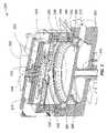
- FIG. 6Ais a perspective view and FIG. 6B is a cross-sectional view, both of a chamber-top assembly for use with a processing chamber according to disclosed embodiments.
- a gas inlet assembly 601introduces gas into the first plasma region 611 .
- Two distinct gas supply channelsare visible within the gas inlet assembly 601 .
- a first channel 602carries a gas that passes through the remote plasma system RPS 600 , while a second channel 603 bypasses the RPS 600 .
- the first channel 602may be used for the process gas and the second channel 603 may be used for a treatment gas in disclosed embodiments.
- the lid 605 and showerhead 615are shown with an insulating ring 610 in between, which allows an AC potential to be applied to the lid 605 relative to the showerhead 615 .
- the side of the substrate processing chamber 625is shown with a gas distribution channel from which tubes may be mounted pointing radially inward. Tubes are not shown in the views of FIGS. 6A-B .
- the showerhead 615 of FIGS. 6A-Bis thicker than the length of the smallest diameter 617 of the holes in this disclosed embodiment.
- the length 618 of the smallest diameter 617 of the holesmay be restricted by forming larger holes 619 part way through the showerhead 615 .
- the length of the smallest diameter 617 of the holesmay be the same order of magnitude as the smallest diameter 617 of the holes or less in disclosed embodiments.
- FIG. 7Ais another cross-sectional view of a dual-source lid for use with a processing chamber according to disclosed embodiments.
- a gas inlet assembly 701introduces gas into the first plasma region 711 .
- Two distinct gas supply channelsare visible within the gas inlet assembly 701 .
- a first channel 702carries a gas that passes through the remote plasma system RPS 700 , while a second channel 703 bypasses the RPS 700 .
- the first channel 702may be used for the process gas and the second channel 703 may be used for a treatment gas in disclosed embodiments.
- the lid 705 and showerhead 715are shown with an insulating ring 710 in between, which allows an AC potential to be applied to the lid 705 relative to the showerhead 715 .
- the showerhead 715 of FIG. 7Ahas through-holes similar to those in FIGS. 6A-B to allow excited derivatives of gases (such as a process gas) to travel from first plasma region 711 into second plasma region 730 .
- the showerhead 715also has one or more hollow volumes 751 which can be filled with a vapor or gas (such as a silicon-containing precursor) and pass through small holes 755 into second plasma region 730 but not into first plasma region 711 . Hollow volumes 751 and small holes 755 may be used in place of tubes for introducing silicon-containing precursors into second plasma region 730 .
- showerhead 715is thicker than the length of the smallest diameter 717 of the through-holes in this disclosed embodiment.
- the length 718 of the smallest diameter 717 of the through-holesmay be restricted by forming larger holes 719 part way through the showerhead 715 .
- the length of the smallest diameter 717 of the through-holesmay be the same order of magnitude as the smallest diameter 617 of the through-holes or less in disclosed embodiments.
- the number of through-holesmay be between about 60 and about 2000.
- Through-holesmay have a variety of shapes but are most easily made round.
- the smallest diameter of through holesmay be between about 0.5 mm and about 20 mm or between about 1 mm and about 6 mm in disclosed embodiments.
- the number of small holes 755 used to introduce a gas into second plasma region 730may be between about 100 and about 5000 or between about 500 and about 2000 in different embodiments.
- the diameter of the small holesmay be between about 0.1 mm and about 2 mm.
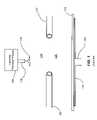
- FIG. 7Bis a bottom view of a showerhead 715 for use with a processing chamber according to disclosed embodiments.
- showerhead 715corresponds with the showerhead shown in FIG. 7A .
- Through-holes 719have a larger inner-diameter (ID) on the bottom of showerhead 715 and a smaller ID at the top.
- Small holes 755are distributed substantially evenly over the surface of the showerhead, even amongst the through-holes 719 which helps to provide more even mixing than other embodiments described herein.
- IDinner-diameter
- FIG. 8shows one such system 800 of deposition, baking and curing chambers according to disclosed embodiments.
- a pair of FOUPs (front opening unified pods) 802supply substrate substrates (e.g., 300 mm diameter wafers) that are received by robotic arms 804 and placed into a low pressure holding area 806 before being placed into one of the wafer processing chambers 808 a - f.
- a second robotic arm 810may be used to transport the substrate wafers from the holding area 806 to the processing chambers 808 a - f and back.
- the processing chambers 808 a - fmay include one or more system components for depositing, annealing, curing and/or etching a flowable dielectric film on the substrate wafer.
- two pairs of the processing chambere.g., 808 c - d and 808 e - f
- the third pair of processing chamberse.g., 808 a - b
- the same two pairs of processing chambersmay be configured to both deposit and anneal a flowable dielectric film on the substrate, while the third pair of chambers (e.g., 808 a - b ) may be used for UV or E-beam curing of the deposited film.
- all three pairs of chamberse.g., 808 a - f ) may be configured to deposit an cure a flowable dielectric film on the substrate.
- two pairs of processing chambersmay be used for both deposition and UV or E-beam curing of the flowable dielectric, while a third pair of processing chambers (e.g. 808 a - b ) may be used for annealing the dielectric film.
- a third pair of processing chamberse.g. 808 a - b
- additional configurations of deposition, annealing and curing chambers for flowable dielectric filmsare contemplated by system 800 .
- one or more of the process chambers 808 a - fmay be configured as a wet treatment chamber. These process chambers include heating the flowable dielectric film in an atmosphere that include moisture.
- embodiments of system 800may include wet treatment chambers 808 a - b and anneal processing chambers 808 c - d to perform both wet and dry anneals on the deposited dielectric film.
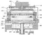
- FIG. 9is a substrate processing chamber 950 according to disclosed embodiments.
- a remote plasma system (RPS) 948may process a gas which then travels through a gas inlet assembly 954 . More specifically, the gas travels through channel 956 into a first plasma region 983 .
- a perforated partition (a showerhead) 952below the first plasma region 983 is a perforated partition (a showerhead) 952 to maintain some physical separation between the first plasma region 983 and a second plasma region 985 beneath the showerhead 952 .
- the showerheadallows a plasma present in the first plasma region 983 to avoid directly exciting gases in the second plasma region 985 , while still allowing excited species to travel from the first plasma region 983 into the second plasma region 985 .
- the showerhead 952is positioned above side nozzles (or tubes) 953 protruding radially into the interior of the second plasma region 985 of the substrate processing chamber 950 .
- the showerhead 952distributes the precursors through a plurality of holes that traverse the thickness of the plate.
- the showerhead 952may have, for example from about 10 to 10000 holes (e.g., 200 holes).
- the showerhead 952may distribute a process gas which contains oxygen, hydrogen and/or nitrogen or derivatives of such process gases upon excitation by a plasma in the first plasma region 983 .
- the process gasmay contain one or more of oxygen (O 2 ), ozone (O 3 ), N 2 O, NO, NO 2 , NH 3 , N x H y including N 2 H 4 , silane, disilane, TSA and DSA.
- the tubes 953may have holes in the end (closest to the center of the second plasma region 985 ) and/or holes distributed around or along the length of the tubes 953 .
- the holesmay be used to introduce a silicon-containing precursor into the second plasma region.
- a filmis created on a substrate supported by a pedestal 986 in the second plasma region 985 when the process gas and its excited derivatives arriving through the holes in the showerhead 952 combine with the silicon-containing precursor arriving through the tubes 953 .
- the top inlet 954may have two or more independent precursor (e.g., gas) flow channels 956 and 958 that keep two or more precursors from mixing and reaction until they enter the first plasma region 983 above the showerhead 952 .
- the first flow channel 956may have an annular shape that surrounds the center of inlet 954 .
- This channelmay be coupled to the remote plasma system (RPS) 948 that generates a reactive species precursor which flows down the channel 956 and into the first plasma region 983 above the showerhead 952 .
- the second flow channel 958may be cylindrically shaped and may be used to flow a second precursor to the first plasma region 983 .
- This flow channelmay start with a precursor and/or carrier gas source that bypasses a reactive species generating unit. The first and second precursors are then mixed and flow through the holes in the plate 952 to the second plasma region.
- first flow channel 956may deliver a process gas that includes one or more of atomic oxygen (in either a ground or electronically excited state), oxygen (O 2 ), ozone (O 3 ), N 2 O, NO, NO 2 , NH 3 , N x H y including N 2 H 4 , silane, disilane, TSA and DSA.
- the process gasmay also include a carrier gas such as helium, argon, nitrogen (N 2 ), etc.
- the second channel 958may also deliver a process gas, a carrier gas, and/or a treatment gas used to remove an unwanted component from the growing or as-deposited film.
- an electrical insulator 976e.g. a ceramic ring is placed between the showerhead and the conducting top portion 982 of the processing chamber to enable an voltage difference to be asserted.
- the presence of the electrical insulator 976ensures that a plasma may be created by the RF power source inside the first plasma region 983 .
- a ceramic ringmay also be placed between the showerhead 952 and the pedestal 986 (not shown in FIG. 9 ) to allow a plasma to be created in the second plasma region 985 . This may be placed above or below the tubes 953 depending on the vertical location of the tubes 953 and whether they have metal content which could result in sparking.
- a plasmamay be ignited either in the first plasma region 983 above the showerhead or the second plasma region 985 below the showerhead and the side nozzles 953 .
- An AC voltage typically in the radio frequency (RF) rangeis applied between the conducting top portion 982 of the processing chamber and the showerhead 952 to ignite the a plasma in the first plasma region 983 during deposition.
- the top plasmais left at low or no power when the bottom plasma 985 is turned on to either cure a film or clean the interior surfaces bordering the second plasma region 985 .
- a plasma in the second plasma region 985is ignited by applying an AC voltage between the showerhead 952 and the pedestal 986 (or bottom of the chamber).
- a gas in an “excited state” as used hereindescribes a gas wherein at least some of the gas molecules are in vibrationally-excited, dissociated and/or ionized states.
- a gasmay be a combination of two or more gases.
- FIG. 10is a flow chart of a deposition process according to disclosed embodiments.
- a substrate processing chamberthat is divided into at least two compartments is used to carry out the methods described herein.
- the substrate processing chambermay have a first plasma region and a second plasma region. Both the first plasma region and the second plasma region may have plasmas ignited within the regions.
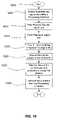
- the process shown in FIG. 10begins with the delivery of a substrate into a substrate processing chamber (Step 1005 ).
- the substrateis placed in the second plasma region after which a process gas may be flowed (Step 1010 ) into the first plasma region.
- a treatment gasmay also be introduced into either the first plasma region or the second plasma region (step not shown).
- a plasmamay then initiated (Step 1015 ) in the first plasma region but not in the second plasma region.
- a silicon-containing precursoris flowed into the second plasma region 1020 .
- the timing and order of steps 1010 , 1015 and 1020may be adjusted without deviating from the spirit of the invention.
- the plasmas and gas flowsare stopped 1030 and the substrate may be removed 1035 from the substrate processing chamber. Before the substrate is removed, the film may be cured in the process described next.
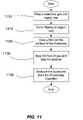
- FIG. 11is a flow chart of a film curing process according to disclosed embodiments.
- the start 1100 of this processmay be just before the substrate is removed 1035 in the method shown in FIG. 10 .
- This processmay also start 1100 by a substrate into the second plasma region of the processing chamber. In this case the substrate may have been processed in another processing chamber.
- a treatment gaspossibly gases described earlier
- Undesirable content in the filmis then removed 1125 .
- this undesirable contentis organic and the process involves curing or hardening 1125 the film on the substrate. The film may shrink during this process.
- the flow of the gas and the plasmaare stopped 1130 and the substrate may be removed 1135 from the substrate processing chamber.
- FIG. 12is a flow chart of a chamber cleaning process according to disclosed embodiments.
- the start 1200 of this processmay occur after a chamber is cleaned or seasoned which often occur after a preventative maintenance (PM) procedure or an unplanned event.
- PMpreventative maintenance
- the substrate processing chamberhas two compartments which may not be able to support plasmas in the first plasma region and the second plasma region simultaneously, a sequential process may be needed to clean both regions.
- a treatment gas(possible gases described earlier) is flowed 1210 into the first plasma region and a plasma is initiated 1215 in the first plasma region (again the timing/order may be adjusted).
- the interior surfaces within the first plasma regionare cleaned 1225 before the flow of the treatment gas and the plasma are stopped 1230 .
- the processis repeated for the second plasma region.
- the treatment gasis flowed 1235 into the second plasma region and a plasma is initiated 1240 therein.
- the interior surfaces of the second plasma regionare cleaned 1245 and the treatment gas flow and plasma are stopped 1250 .
- Interior surface cleaning proceduresmay be conducted to clean fluorine from the interior surfaces of the substrate processing chamber as well as other leftover contaminants from troubleshooting and maintenance procedures.
Landscapes
- Chemical & Material Sciences (AREA)
- Engineering & Computer Science (AREA)
- General Chemical & Material Sciences (AREA)
- Chemical Kinetics & Catalysis (AREA)
- Materials Engineering (AREA)
- Mechanical Engineering (AREA)
- Metallurgy (AREA)
- Organic Chemistry (AREA)
- Physics & Mathematics (AREA)
- Plasma & Fusion (AREA)
- Analytical Chemistry (AREA)
- Chemical Vapour Deposition (AREA)
Abstract
Description
- This application claims the benefit of U.S. Provisional Patent Application No. 61/052,080 field May 9, 2008. This application is also related to U.S. patent application Ser. No. 11/754,858, filed May 29, 2007, and titled “PROCESS CHAMBER FOR DIELECTRIC GAPFILL.” The entire contents of both applications are herein incorporated by reference for all purposes.
- This application relates to manufacturing technology solutions involving equipment, processes, and materials used in the deposition, patterning, and treatment of thin-films and coatings, with representative examples including (but not limited to) applications involving: semiconductor and dielectric materials and devices, silicon-based wafers and flat panel displays (such as TFTs).
- A conventional semiconductor processing system contains one or more processing chambers and a means for moving a substrate between them. A substrate may be transferred between chambers by a robotic arm which can extend to pick up the substrate, retract and then extend again to position the substrate in a different destination chamber.
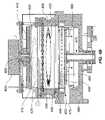
FIG. 1 shows a schematic of a substrate processing chamber. Each chamber has apedestal shaft 105 andpedestal 110 or some equivalent way of supporting thesubstrate 115 for processing. - A pedestal can be a heater plate in a processing chamber configured to heat the substrate. The substrate may be held by a mechanical, pressure differential or electrostatic means to the pedestal between when a robot arm drops off the substrate and when an arm returns to pick up the substrate. Lift pins are often used to elevate the wafer during robot operations.
- One or more semiconductor fabrication process steps are performed in the chamber, such as annealing the substrate or depositing or etching films on the substrate. Dielectric films are deposited into complex topologies during some processing steps. Many techniques have been developed to deposit dielectrics into narrow gaps including variations of chemical vapor deposition techniques which sometimes employ plasma techniques. High-density plasma (HDP)-CVD has been used to fill many geometries due to the perpendicular impingement trajectories of the incoming reactants and the simultaneous sputtering activity. Some very narrow gaps, however, have continued to develop voids due, in part, to the lack of mobility following initial impact. Reflowing the material after deposition can fill the void but, if the dielectric has a high reflow temperature (like SiO2), the reflow process may also consume a non-negligible portion of a wafer's thermal budget.
- By way of its high surface mobility, flow-able materials such as spin-on glass (SOG) have been useful in filling some of the gaps which were incompletely filled by HDP-CVD. SOG is applied as a liquid and cured after application to remove solvents, thereby converting material to a solid glass film. The gap-filling (gapfill) and planarization capabilities are enhanced for SOG when the viscosity is low. Unfortunately, low viscosity materials may shrink significantly during cure. Significant film shrinkage results in high film stress and delamination issues, especially for thick films.
- Separating the delivery paths of two components can produce a flowable film during deposition on a substrate surface.
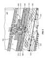
FIG. 1 shows a schematic of a substrate processing system withseparated delivery channels remote plasma 145. Themixing region 120 of the two components occurs closer to thesubstrate 115 than alternative processes utilizing a more common delivery path. Since the films are grown rather than poured onto the surface, the organic components needed to decrease viscosity are allowed to evaporate during the process which reduces the shrinkage affiliated with a cure step. Growing films this way limits the time available for adsorbed species to remain mobile, a constraint which may result in deposition of nonuniform films. Abaffle 140 may be used to more evenly distribute the precursors in the reaction region. - Gapfill capabilities and deposition uniformity benefit from high surface mobility which correlates with high organic content. Some of the organic content may remain after deposition and a cure step may be used. The cure may be conducted by raising the temperature of the
pedestal 110 andsubstrate 115 with a resistive heater embedded in the pedestal. - Embodiments of the invention include methods of depositing and curing a dielectric material on a substrate. The methods may include the steps of providing a processing chamber partitioned into a first plasma region and a second plasma region, and delivering the substrate to the processing chamber, where the substrate occupies a portion of the second plasma region. The methods may further include forming a first plasma in the first plasma region, where the first plasma does not directly contact with the substrate, and depositing the dielectric material on the substrate to form a dielectric layer. One or more reactants excited by the first plasma are used in the deposition of the dielectric material. The methods may additional include curing the dielectric layer by forming a second plasma in the second plasma region, wherein one or more carbon-containing species is removed from the dielectric layer.
- Embodiments of the invention also include methods of depositing a film on a substrate disposed in a processing chamber. The methods may include the steps of flowing a first process gas mixture into a substrate processing region to form a film on the substrate. The methods may also include flowing a treatment gas through a plasma, through a showerhead, and into the substrate processing region to remove undesirable components from the film during growth.
- Embodiments of the invention still further include methods of cleaning interior surfaces of a processing chamber partitioned by a showerhead into a first plasma region and a second plasma region. The methods may include the steps of flowing a treatment gas into the first plasma region, igniting a plasma in the first plasma region, and igniting a plasma in the second plasma region.
- Embodiments of the invention may also include substrate processing systems that have a processing chamber and a substrate support assembly at least partially disposed within the chamber. Two gases (or two combinations of gases) are delivered to the substrate processing chamber by different paths. A process gas can be delivered into the processing chamber, excited in a plasma in a first plasma region, and pass through a showerhead into a second plasma region where it interacts with a silicon-containing gas and forms a film on the surface of a substrate. A plasma may be ignited in either the first plasma region or the second plasma region.
- Choosing the orientation arbitrarily, the process gas can be introduced through a top of the processing chamber which forms a top plasma electrode. The showerhead forms a middle plasma electrode and the bottom of the processing chamber and/or the pedestal form the bottom electrode. The middle electrode can be chosen to substantially match the top or the bottom electrodes thereby determining the location of the plasma. During deposition, a plasma is ignited with the top and middle electrodes to form a plasma in the first plasma region. The potential of the middle electrode may be chosen to substantially match the top electrode, thereby creating a plasma in the second plasma region. A plasma in the second plasma region may help cure a deposited film but can also be used to clean the chamber. During a cleaning process, the gas present in the second plasma region may contain fluorine.
- The process gas may contain oxygen, hydrogen and/or nitrogen (e.g. oxygen (O2), ozone (O3), N2O, NO, NO2, NH3, NxHyincluding N2H4, silane, disilane, TSA, DSA, etc.), and after it passes the showerhead, it is combined with a silicon-containing precursor (e.g. silane, disilane, TSA, DSA, TEOS, OMCTS, TMDSO, etc.) and introduced into the second plasma region. The combination of reactants forms a film of film on a substrate. The film may be silicon oxide, silicon nitride, silicon oxycarbide or silicon oxynitride.
- Embodiments may also include introducing a treatment gas such as oxygen (O2), ozone (O3), N2O, NO, NO2, NxHyincluding N2H4, H2, N2, NH3, and water vapor. The treatment gas may be introduced from the top of the processing chamber and excited in the first plasma region. Alternatively, the gas may be excited by a remote plasma before entering the first plasma region. This gas does not contribute appreciably to the film growth, but may be used to reduce hydrogen, carbon and fluorine content of the film while it is being grown or following growth. Hydrogen and nitrogen radicals induce a reduction in undesirable components of the growing film. Excited derivatives of the treatment gas assist the film by scavenging carbon and other atoms from the growing lattice, thereby reducing the contraction exhibited during the cure and the film stress present afterward.
- In further embodiments, a treatment gas is delivered through showerhead, after being excited in a remote plasma or a plasma in the first plasma region, to the second plasma region after a chamber maintenance procedure (clean and/or season) to remove residual fluorine from the interior of the processing chamber.
- The two plasmas can be a variety of frequencies but will generally be in the radio frequency (RF) range. The plasmas can be inductively or capacitively coupled. All parts of the chamber including the showerhead may be cooled by flowing water or another coolant through channels made in the parts.
- Additional embodiments and features are set forth in part in the description that follows, and in part will become apparent to those skilled in the art upon examination of the specification or may be learned by the practice of the disclosed embodiments. The features and advantages of the disclosed embodiments may be realized and attained by means of the instrumentalities, combinations, and methods described in the specification.
- A further understanding of the nature and advantages of the disclosed embodiments may be realized by reference to the remaining portions of the specification and the drawings.
FIG. 1 is a schematic of a prior art processing region within a deposition chamber for growing films with separate oxidizing and organo-silane precursors.FIG. 2 is a perspective view of a process chamber with partitioned plasma generation regions according to disclosed embodiments.FIG. 3A is a schematic of an electrical switch box according to disclosed embodiments.FIG. 3B is a schematic of an electrical switch box according to disclosed embodiments.FIG. 4A is a cross-sectional view of a process chamber with partitioned plasma generation regions according to disclosed embodiments.FIG. 4B is a cross-sectional view of a process chamber with partitioned plasma generation regions according to disclosed embodiments.FIG. 5 is a close-up perspective view of a gas inlet and first plasma region according to disclosed embodiments.FIG. 6A is a perspective view of a dual-source lid for use with a processing chamber according to disclosed embodiments.FIG. 6B is a cross-sectional view of a dual-source lid for use with a processing chamber according to disclosed embodiments.FIG. 7A is a cross-sectional view of a dual-source lid for use with a processing chamber according to disclosed embodiments.FIG. 7B is a bottom view of a showerhead for use with a processing chamber according to disclosed embodiments.FIG. 8 is a substrate processing system according to disclosed embodiments.FIG. 9 is a substrate processing chamber according to disclosed embodiments.FIG. 10 is a flow chart of a deposition process according to disclosed embodiments.FIG. 11 is a flow chart of a film curing process according to disclosed embodiments.FIG. 12 is a flow chart of a chamber cleaning process according to disclosed embodiments.- In the appended figures, similar components and/or features may have the same reference label. Where the reference label is used in the specification, the description is applicable to any one of the similar components having the same reference label.
- Disclosed embodiments include substrate processing systems that have a processing chamber and a substrate support assembly at least partially disposed within the chamber. At least two gases (or two combinations of gases) are delivered to the substrate processing chamber by different paths. A process gas can be delivered into the processing chamber, excited in a plasma, and pass through a showerhead into a second plasma region where it interacts with a silicon-containing gas and forms a film on the surface of a substrate. A plasma can be ignited in either the first plasma region or the second plasma region.
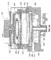
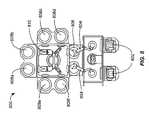
FIG. 2 is a perspective view of a process chamber with partitioned plasma generation regions which maintain a separation between multiple gas precursors. A process gas containing oxygen, hydrogen and/or nitrogen (e.g. oxygen (O2), ozone (O3), N2O, NO, NO2, NH3, NxHyincluding N2H4, silane, disilane, TSA, DSA, . . . ) may be introduced through thegas inlet assembly 225 into afirst plasma region 215. Thefirst plasma region 215 may contain a plasma formed from the process gas. The process gas may also be excited prior to entering thefirst plasma region 215 in a remote plasma system (RPS)220. Below thefirst plasma region 215 is ashowerhead 210, which is a perforated partition (referred to herein as a showerhead) between thefirst plasma region 215 and asecond plasma region 242. In embodiments, a plasma in thefirst plasma region 215 is created by applying AC power, possibly RF power, between alid 204 and theshowerhead 210, which may also be conducting.- In order to enable the formation of a plasma in the first plasma region, an electrically insulating
ring 205 may be positioned between thelid 204 and theshowerhead 210 to enable an RF power to be applied between thelid 204 and theshowerhead 210. The electrically insulatingring 205 may be made from a ceramic and may have a high breakdown voltage to avoid sparking. - The
second plasma region 242 may receive excited gas from thefirst plasma region 215 through holes in theshowerhead 210. Thesecond plasma region 242 may also receive gases and/or vapors fromtubes 230 extending from aside 235 of theprocessing chamber 200. The gas from thefirst plasma region 215 and the gas from thetubes 230 are mixed in thesecond plasma region 242 to process thesubstrate 255. Igniting a plasma in thefirst plasma region 215 to excite the process gas, may result in a more uniform distribution of excited species flowing into the substrate processing region (second plasma region242) than a method relying only on theRPS 145 and baffle140 ofFIG. 1 . In disclosed embodiments, there is no plasma in thesecond plasma region 242. - Processing the
substrate 255 may include forming a film on the surface of thesubstrate 255 while the substrate is supported by apedestal 265 positioned within thesecond plasma region 242. Theside 235 of theprocessing chamber 200 may contain a gas distribution channel which distributes the gas to thetubes 230. In embodiments, silicon-containing precursors are delivered from the gas distribution channel through thetubes 230 and through an aperture at the end of eachtube 230 and/or apertures along the length of thetubes 230. - Note that the path of the gas entering the
first plasma region 215 from thegas inlet 225 can be interrupted by a baffle (not shown, but analogous to thebaffle 140 ofFIG. 1 ) whose purpose here is to more evenly distribute the gas in thefirst plasma region 215. In some disclosed embodiments, the process gas is an oxidizing precursor (which may containing oxygen (O2), ozone (O3), . . . ) and after flowing through the holes in the showerhead, the process gas may be combined with a silicon-containing precursor (e.g. silane, disilane, TSA, DSA, TEOS, OMCTS, TMDSO, . . . ) introduced more directly into the second plasma region. The combination of reactants may be used to form a film of silicon oxide (SiO2) on asubstrate 255. In embodiments the process gas contains nitrogen (NH3, NxHyincluding N2H4, TSA, DSA, N2O, NO, NO2, . . . ) which, when combined with a silicon-containing precursor may be used to form silicon nitride, silicon oxynitride or a low-K dielectric. - In disclosed embodiments, a substrate processing system is also configured so a plasma may be ignited in the
second plasma region 242 by applying an RF power between theshowerhead 210 and thepedestal 265. When asubstrate 255 is present, the RF power may be applied between theshowerhead 210 and thesubstrate 255. An insulatingspacer 240 is installed between theshowerhead 210 and thechamber body 280 to allow theshowerhead 210 to be held at a different potential from thesubstrate 255. Thepedestal 265 is supported by apedestal shaft 270. Asubstrate 255 may be delivered to theprocess chamber 200 through aslit valve 275 and may be supported bylift pins 260 before being lowered onto thepedestal 265. - In the above description, plasmas in the
first plasma region 215 and thesecond plasma region 242 are created by applying an RF power between parallel plates. In an alternative embodiment, either or both plasmas may be created inductively in which case the two plates may not be conducting. Conducting coils may be embedded within two electrically insulating plates and/or within electrically insulating walls of the processing chamber surrounding the region. Regardless of whether a plasma is capacitively coupled (CCP) or inductively coupled (ICP), the portions of the chamber exposed to the plasma may be cooled by flowing water through a cooling fluid channel within the portion. Theshower head 210, thelid 204 and thewalls 205 are water-cooled in disclosed embodiments. In the event that an inductively coupled plasma is used, the chamber may (more easily) be operated with plasmas in both the first plasma region and the second plasma region at the same time. This capability may be useful to expedite chamber cleaning. FIGS. 3A-B are electrical schematics of anelectrical switch 300 which may result in a plasma in either the first plasma region or the second plasma region. In bothFIGS. 3A and 3B theelectrical switch 300 is a modified double-pole double-throw (DPDT). Theelectrical switch 300 can be in one of two positions. The first position is shown inFIG. 3A and the second position inFIG. 3B . The two connections on the left are electrical inputs to the processing chamber and the two connections on the right are output connections to components on the processing chamber. Theelectrical switch 300 may be located physically near or on the processing chamber but may also be distal to the processing chamber. Theelectrical switch 300 may be manually and/or automatically operated. Automatic operation may involve the use of one or more relays to change the status of the twocontacts electrical switch 300 in this disclosed embodiment is modified from a standard DPDT switch in that exactly oneoutput 312 can be contacted by each of the twocontacts contact 306.- The first position (
FIG. 3A ) enables a plasma to be created in the first plasma region and results in little or no plasma in the second plasma region. The chamber body, pedestal and substrate (if present) are typically at ground potential in most substrate processing systems. In disclosed embodiments, the pedestal is grounded regardless of theelectrical switch 300 position.FIG. 3A shows a switch position which applies an RF power to thelid 370 and grounds (in other words applies 0 volts to) theshowerhead 375. This switch position may correspond to the deposition of a film on the substrate surface. - The second position (
FIG. 3B ) enables a plasma to be created in the second plasma region.FIG. 3B shows a switch position which applies an RF power to theshowerhead 375 and allows thelid 370 to float. An electrically floatinglid 370 results in little or no plasma present in the first plasma region. This switch position may correspond to the treatment of a film after deposition or to a chamber cleaning procedure in disclosed embodiments. - Two
impedance matching circuits lid 370 andshowerhead 375 are depicted in bothFIGS. 3A and 3B . Theimpedance matching circuits FIGS. 4A-B are cross-sectional views of a process chamber with partitioned plasma generation regions according to disclosed embodiments. During film deposition (silicon oxide, silicon nitride, silicon oxynitride or silicon oxycarbide), a process gas may be flowed into thefirst plasma region 415 through agas inlet assembly 405. The process gas may be excited prior to entering thefirst plasma region 415 within a remote plasma system (RPS)400. Alid 412 andshowerhead 425 are shown according to disclosed embodiments. Thelid 412 is depicted (FIG. 4A ) with an applied AC voltage source and the showerhead is grounded, consistent with the first position of the electrical switch inFIG. 3A . An insulatingring 420 is positioned between thelid 412 and theshowerhead 425 enabling a capacitively coupled plasma (CCP) to be formed in the first plasma region.- A silicon-containing precursor may be flowed into the
second plasma region 433 throughtubes 430 extending from thesides 435 of the processing chamber. Excited species derived from the process gas travel through holes in theshowerhead 425 and react with the silicon-containing precursor flowing through thesecond plasma region 433. The diameter of holes in theshowerhead 425 may be below 12 mm, may be between 0.25 mm and 8 mm, and may be between 0.5 mm and 6 mm in different embodiments. The thickness of the showerhead can vary quite a bit but the length of the diameter of the holes may be about the diameter of the holes or less, increasing the density of the excited species derived from the process gas within thesecond plasma region 433. Little or no plasma is present in thesecond plasma region 433 due to the position of the switch (FIG. 3A ). Excited derivatives of the process gas and the silicon-containing precursor combine in the region above the substrate and, on occasion, on the substrate to form a flowable film on the substrate. As the film grows, more recently added material possesses a higher mobility than underlying material. Mobility decreases as organic content is reduced by evaporation. Gaps may be filled by the flowable film using this technique without leaving traditional densities of organic content within the film after deposition is completed. A curing step may still be used to further reduce or remove the organic content from a deposited film. - Exciting the process gas in the
first plasma region 415 alone or in combination with the remote plasma system (RPS) provides several benefits. The concentration of the excited species derived from the process gas may be increased within thesecond plasma region 433 due to the plasma in thefirst plasma region 415. This increase may result from the location of the plasma in thefirst plasma region 415. Thesecond plasma region 433 is located closer to thefirst plasma region 415 than the remote plasma system (RPS)400, leaving less time for the excited species to leave excited states through collisions with other gas molecules, walls of the chamber and surfaces of the showerhead. - The uniformity of the concentration of the excited species derived from the process gas may also be increased within the
second plasma region 433. This may result from the shape of thefirst plasma region 415, which is more similar to the shape of thesecond plasma region 433. Excited species created in the remote plasma system (RPS)400 travel greater distances in order to pass through holes near the edges of theshowerhead 425 relative to species that pass through holes near the center of theshowerhead 425. The greater distance results in a reduced excitation of the excited species and, for example, may result in a slower growth rate near the edge of a substrate. Exciting the process gas in thefirst plasma region 415 mitigates this variation. - In addition to the process gas and silicon-containing precursor there may be other gases introduced at varied times for varied purposes. A treatment gas may be introduced to remove unwanted species from the chamber walls, the substrate, the deposited film and/or the film during deposition. The treatment gas may comprise at least one of the gases from the group: H2, an H2/N2mixture, NH3, NH4OH, O3, O2, H2O2and water vapor. A treatment gas may be excited in a plasma and then used to reduce or remove a residual organic content from the deposited film. In other disclosed embodiments the treatment gas may be used without a plasma. When the treatment gas includes water vapor, the delivery may be achieved using a mass flow meter (MFM) and injection valve or by commercially available water vapor generators.
FIG. 4B is a cross-sectional view of a process chamber with a plasma in thesecond plasma region 433 consistent with the switch position shown inFIG. 3B . A plasma may be used in thesecond plasma region 433 to excite a treatment gas delivered through thetubes 430 extending from thesides 435 of the processing chamber. Little or no plasma is present in thefirst plasma region 415 due to the position of the switch (FIG. 3B ). Excited species derived from the treatment gas react with the film on thesubstrate 455 and remove organic compounds from the deposited film. Herein this process may be referred to as treating or curing the film.- The
tubes 430 in thesecond plasma region 433 comprise insulating material, such as aluminum nitride or aluminum oxide, in some disclosed embodiments. An insulating material reduces the risk of sparking for some substrate processing chamber architectures. - The treatment gas may also be introduced through the
gas inlet assembly 405 into thefirst plasma region 415. In disclosed embodiments the treatment gas may be introduced through thegas inlet assembly 405 alone or in combination with a flow of treatment gas through thetubes 430 extending from thewalls 435 of thesecond plasma region 433. A treatment gas flowing through thefirst plasma region 415 and then through theshowerhead 430 to treat a deposited film may be excited in a plasma in thefirst plasma region 415 or alternatively in a plasma in thesecond plasma region 433. - In addition to treating or curing the
substrate 455, a treatment gas may be flowed into thesecond plasma region 433 with a plasma present to clean the interior surfaces (e.g.walls 435,showerhead 425,pedestal 465 and tubes430) of thesecond plasma region 433. Similarly, a treatment gas may be flowed into thefirst plasma region 415 with a plasma present to clean the interior of the surfaces (e.g. lid 412,walls 420 and showerhead425) of thefirst plasma region 415. In disclosed embodiments, a treatment gas is flowed into the second plasma region433 (with a plasma present) after a second plasma region maintenance procedure (clean and/or season) to remove residual fluorine from the interior surfaces of thesecond plasma region 433. As part of a separate procedure or a separate step (possibly sequential) of the same procedure, the treatment gas is flowed into the first plasma region415 (with a plasma present) after a first plasma region maintenance procedure (clean and/or season) to remove residual fluorine from the interior surfaces of thefirst plasma region 415. Generally, both regions will be in need of cleaning or seasoning at the same time and the treatment gas may treat each region sequentially before substrate processing resumes. - The aforementioned treatment gas processes use a treatment gas in process steps distinct from the deposition step. A treatment gas may also be used during deposition to remove organic content from the growing film.
FIG. 5 shows a close-up perspective view of thegas inlet assembly 503 and thefirst plasma region 515. Thegas inlet assembly 503 is shown in finer detail revealing two distinctgas flow channels first plasma region 515 through anexterior channel 505. The process gas may or may not be excited by theRPS 500. A treatment gas may flow into thefirst plasma region 515 from aninterior channel 510, without being excited by theRPS 500. The locations of theexterior channel 505 and theinterior channel 510 may be arranged in a variety of physical configurations (e.g. the RPS excited gas may flow through the interior channel in disclosed embodiments) such that only one of the two channels flows through theRPS 500. - Both the process gas and the treatment gas may be excited in a plasma in the
first plasma region 515 and subsequently flow into the second plasma region through holes in theshowerhead 520. The purpose of the treatment gas is to remove unwanted components (generally organic content) from the film during deposition. In the physical configuration shown inFIG. 5 , the gas from theinterior channel 510 may not contribute appreciably to the film growth, but may be used to scavenge fluorine, hydrogen and/or carbon from the growing film. FIG. 6A is a perspective view andFIG. 6B is a cross-sectional view, both of a chamber-top assembly for use with a processing chamber according to disclosed embodiments. Agas inlet assembly 601 introduces gas into thefirst plasma region 611. Two distinct gas supply channels are visible within thegas inlet assembly 601. Afirst channel 602 carries a gas that passes through the remoteplasma system RPS 600, while asecond channel 603 bypasses theRPS 600. Thefirst channel 602 may be used for the process gas and thesecond channel 603 may be used for a treatment gas in disclosed embodiments. Thelid 605 andshowerhead 615 are shown with an insulatingring 610 in between, which allows an AC potential to be applied to thelid 605 relative to theshowerhead 615. The side of thesubstrate processing chamber 625 is shown with a gas distribution channel from which tubes may be mounted pointing radially inward. Tubes are not shown in the views ofFIGS. 6A-B .- The
showerhead 615 ofFIGS. 6A-B is thicker than the length of thesmallest diameter 617 of the holes in this disclosed embodiment. In order to maintain a significant concentration of excited species penetrating from thefirst plasma region 611 to thesecond plasma region 630, thelength 618 of thesmallest diameter 617 of the holes may be restricted by forminglarger holes 619 part way through theshowerhead 615. The length of thesmallest diameter 617 of the holes may be the same order of magnitude as thesmallest diameter 617 of the holes or less in disclosed embodiments. FIG. 7A is another cross-sectional view of a dual-source lid for use with a processing chamber according to disclosed embodiments. Agas inlet assembly 701 introduces gas into thefirst plasma region 711. Two distinct gas supply channels are visible within thegas inlet assembly 701. Afirst channel 702 carries a gas that passes through the remoteplasma system RPS 700, while asecond channel 703 bypasses theRPS 700. Thefirst channel 702 may be used for the process gas and thesecond channel 703 may be used for a treatment gas in disclosed embodiments. Thelid 705 andshowerhead 715 are shown with an insulatingring 710 in between, which allows an AC potential to be applied to thelid 705 relative to theshowerhead 715.- The
showerhead 715 ofFIG. 7A has through-holes similar to those inFIGS. 6A-B to allow excited derivatives of gases (such as a process gas) to travel fromfirst plasma region 711 intosecond plasma region 730. Theshowerhead 715 also has one or morehollow volumes 751 which can be filled with a vapor or gas (such as a silicon-containing precursor) and pass throughsmall holes 755 intosecond plasma region 730 but not intofirst plasma region 711.Hollow volumes 751 andsmall holes 755 may be used in place of tubes for introducing silicon-containing precursors intosecond plasma region 730.Showerhead 715 is thicker than the length of thesmallest diameter 717 of the through-holes in this disclosed embodiment. In order to maintain a significant concentration of excited species penetrating from thefirst plasma region 711 to thesecond plasma region 730, thelength 718 of thesmallest diameter 717 of the through-holes may be restricted by forminglarger holes 719 part way through theshowerhead 715. The length of thesmallest diameter 717 of the through-holes may be the same order of magnitude as thesmallest diameter 617 of the through-holes or less in disclosed embodiments. - In embodiments, the number of through-holes may be between about 60 and about 2000. Through-holes may have a variety of shapes but are most easily made round. The smallest diameter of through holes may be between about 0.5 mm and about 20 mm or between about 1 mm and about 6 mm in disclosed embodiments. There is also latitude in choosing the cross-sectional shape of through-holes, which may be made conical, cylindrical or a combination of the two shapes. The number of
small holes 755 used to introduce a gas intosecond plasma region 730 may be between about 100 and about 5000 or between about 500 and about 2000 in different embodiments. The diameter of the small holes may be between about 0.1 mm and about 2 mm. FIG. 7B is a bottom view of ashowerhead 715 for use with a processing chamber according to disclosed embodiments.Showerhead 715 corresponds with the showerhead shown inFIG. 7A . Through-holes 719 have a larger inner-diameter (ID) on the bottom ofshowerhead 715 and a smaller ID at the top.Small holes 755 are distributed substantially evenly over the surface of the showerhead, even amongst the through-holes 719 which helps to provide more even mixing than other embodiments described herein.- Embodiments of the deposition systems may be incorporated into larger fabrication systems for producing integrated circuit chips.
FIG. 8 shows onesuch system 800 of deposition, baking and curing chambers according to disclosed embodiments. In the figure, a pair of FOUPs (front opening unified pods)802 supply substrate substrates (e.g., 300 mm diameter wafers) that are received byrobotic arms 804 and placed into a lowpressure holding area 806 before being placed into one of the wafer processing chambers808a-f.A secondrobotic arm 810 may be used to transport the substrate wafers from the holdingarea 806 to the processing chambers808a-fand back. - The processing chambers808a-fmay include one or more system components for depositing, annealing, curing and/or etching a flowable dielectric film on the substrate wafer. In one configuration, two pairs of the processing chamber (e.g.,808c-dand808e-f) may be used to deposit the flowable dielectric material on the substrate, and the third pair of processing chambers (e.g.,808a-b) may be used to anneal the deposited dialectic. In another configuration, the same two pairs of processing chambers (e.g.,808c-dand808e-f) may be configured to both deposit and anneal a flowable dielectric film on the substrate, while the third pair of chambers (e.g.,808a-b) may be used for UV or E-beam curing of the deposited film. In still another configuration, all three pairs of chambers (e.g.,808a-f) may be configured to deposit an cure a flowable dielectric film on the substrate. In yet another configuration, two pairs of processing chambers (e.g.,808c-dand808e-f) may be used for both deposition and UV or E-beam curing of the flowable dielectric, while a third pair of processing chambers (e.g.808a-b) may be used for annealing the dielectric film. It will be appreciated, that additional configurations of deposition, annealing and curing chambers for flowable dielectric films are contemplated by
system 800. - In addition, one or more of the process chambers808a-fmay be configured as a wet treatment chamber. These process chambers include heating the flowable dielectric film in an atmosphere that include moisture. Thus, embodiments of
system 800 may include wet treatment chambers808a-bandanneal processing chambers 808c-dto perform both wet and dry anneals on the deposited dielectric film. FIG. 9 is asubstrate processing chamber 950 according to disclosed embodiments. A remote plasma system (RPS)948 may process a gas which then travels through agas inlet assembly 954. More specifically, the gas travels throughchannel 956 into afirst plasma region 983. Below thefirst plasma region 983 is a perforated partition (a showerhead)952 to maintain some physical separation between thefirst plasma region 983 and asecond plasma region 985 beneath theshowerhead 952. The showerhead allows a plasma present in thefirst plasma region 983 to avoid directly exciting gases in thesecond plasma region 985, while still allowing excited species to travel from thefirst plasma region 983 into thesecond plasma region 985.- The
showerhead 952 is positioned above side nozzles (or tubes)953 protruding radially into the interior of thesecond plasma region 985 of thesubstrate processing chamber 950. Theshowerhead 952 distributes the precursors through a plurality of holes that traverse the thickness of the plate. Theshowerhead 952 may have, for example from about 10 to 10000 holes (e.g., 200 holes). In the embodiment shown, theshowerhead 952 may distribute a process gas which contains oxygen, hydrogen and/or nitrogen or derivatives of such process gases upon excitation by a plasma in thefirst plasma region 983. In embodiments, the process gas may contain one or more of oxygen (O2), ozone (O3), N2O, NO, NO2, NH3, NxHyincluding N2H4, silane, disilane, TSA and DSA. - The
tubes 953 may have holes in the end (closest to the center of the second plasma region985) and/or holes distributed around or along the length of thetubes 953. The holes may be used to introduce a silicon-containing precursor into the second plasma region. A film is created on a substrate supported by apedestal 986 in thesecond plasma region 985 when the process gas and its excited derivatives arriving through the holes in theshowerhead 952 combine with the silicon-containing precursor arriving through thetubes 953. - The
top inlet 954 may have two or more independent precursor (e.g., gas)flow channels first plasma region 983 above theshowerhead 952. Thefirst flow channel 956 may have an annular shape that surrounds the center ofinlet 954. This channel may be coupled to the remote plasma system (RPS)948 that generates a reactive species precursor which flows down thechannel 956 and into thefirst plasma region 983 above theshowerhead 952. Thesecond flow channel 958 may be cylindrically shaped and may be used to flow a second precursor to thefirst plasma region 983. This flow channel may start with a precursor and/or carrier gas source that bypasses a reactive species generating unit. The first and second precursors are then mixed and flow through the holes in theplate 952 to the second plasma region. - The
showerhead 952 andtop inlet 954 may be used to deliver the process gas to thesecond plasma region 985 in thesubstrate processing chamber 950. For example,first flow channel 956 may deliver a process gas that includes one or more of atomic oxygen (in either a ground or electronically excited state), oxygen (O2), ozone (O3), N2O, NO, NO2, NH3, NxHyincluding N2H4, silane, disilane, TSA and DSA. The process gas may also include a carrier gas such as helium, argon, nitrogen (N2), etc. Thesecond channel 958 may also deliver a process gas, a carrier gas, and/or a treatment gas used to remove an unwanted component from the growing or as-deposited film. - For a capacitively coupled plasma (CCP), an electrical insulator976 (e.g. a ceramic ring) is placed between the showerhead and the conducting
top portion 982 of the processing chamber to enable an voltage difference to be asserted. The presence of theelectrical insulator 976 ensures that a plasma may be created by the RF power source inside thefirst plasma region 983. Similarly, a ceramic ring may also be placed between theshowerhead 952 and the pedestal986 (not shown inFIG. 9 ) to allow a plasma to be created in thesecond plasma region 985. This may be placed above or below thetubes 953 depending on the vertical location of thetubes 953 and whether they have metal content which could result in sparking. - A plasma may be ignited either in the
first plasma region 983 above the showerhead or thesecond plasma region 985 below the showerhead and theside nozzles 953. An AC voltage typically in the radio frequency (RF) range is applied between the conductingtop portion 982 of the processing chamber and theshowerhead 952 to ignite the a plasma in thefirst plasma region 983 during deposition. The top plasma is left at low or no power when thebottom plasma 985 is turned on to either cure a film or clean the interior surfaces bordering thesecond plasma region 985. A plasma in thesecond plasma region 985 is ignited by applying an AC voltage between theshowerhead 952 and the pedestal986 (or bottom of the chamber). - A gas in an “excited state” as used herein describes a gas wherein at least some of the gas molecules are in vibrationally-excited, dissociated and/or ionized states. A gas may be a combination of two or more gases.
- Disclosed embodiments include methods which may pertain to deposition, etching, curing, and/or cleaning processes.
FIG. 10 is a flow chart of a deposition process according to disclosed embodiments. A substrate processing chamber that is divided into at least two compartments is used to carry out the methods described herein. The substrate processing chamber may have a first plasma region and a second plasma region. Both the first plasma region and the second plasma region may have plasmas ignited within the regions. - The process shown in
FIG. 10 begins with the delivery of a substrate into a substrate processing chamber (Step1005). The substrate is placed in the second plasma region after which a process gas may be flowed (Step1010) into the first plasma region. A treatment gas may also be introduced into either the first plasma region or the second plasma region (step not shown). A plasma may then initiated (Step1015) in the first plasma region but not in the second plasma region. A silicon-containing precursor is flowed into thesecond plasma region 1020. The timing and order ofsteps FIG. 11 is a flow chart of a film curing process according to disclosed embodiments. The start1100 of this process may be just before the substrate is removed1035 in the method shown inFIG. 10 . This process may also start1100 by a substrate into the second plasma region of the processing chamber. In this case the substrate may have been processed in another processing chamber. A treatment gas (possible gases described earlier) is flowed1110 into the first plasma region and a plasma is initiated1115 in the first plasma region (again the timing/order may be adjusted). Undesirable content in the film is then removed1125. In some disclosed embodiments, this undesirable content is organic and the process involves curing or hardening1125 the film on the substrate. The film may shrink during this process. The flow of the gas and the plasma are stopped1130 and the substrate may be removed1135 from the substrate processing chamber.FIG. 12 is a flow chart of a chamber cleaning process according to disclosed embodiments. The start1200 of this process may occur after a chamber is cleaned or seasoned which often occur after a preventative maintenance (PM) procedure or an unplanned event. Because the substrate processing chamber has two compartments which may not be able to support plasmas in the first plasma region and the second plasma region simultaneously, a sequential process may be needed to clean both regions. A treatment gas (possible gases described earlier) is flowed1210 into the first plasma region and a plasma is initiated1215 in the first plasma region (again the timing/order may be adjusted). The interior surfaces within the first plasma region are cleaned1225 before the flow of the treatment gas and the plasma are stopped1230. The process is repeated for the second plasma region. The treatment gas is flowed1235 into the second plasma region and a plasma is initiated1240 therein. The interior surfaces of the second plasma region are cleaned1245 and the treatment gas flow and plasma are stopped1250. Interior surface cleaning procedures may be conducted to clean fluorine from the interior surfaces of the substrate processing chamber as well as other leftover contaminants from troubleshooting and maintenance procedures.- Having disclosed several embodiments, it will be recognized by those of skill in the art that various modifications, alternative constructions, and equivalents may be used without departing from the spirit of the disclosed embodiments. Additionally, a number of well known processes and elements have not been described in order to avoid unnecessarily obscuring the present invention. Accordingly, the above description should not be taken as limiting the scope of the invention.
- Where a range of values is provided, it is understood that each intervening value, to the tenth of the unit of the lower limit unless the context clearly dictates otherwise, between the upper and lower limits of that range is also specifically disclosed. Each smaller range between any stated value or intervening value in a stated range and any other stated or intervening value in that stated range is encompassed. The upper and lower limits of these smaller ranges may independently be included or excluded in the range, and each range where either, neither or both limits are included in the smaller ranges is also encompassed within the invention, subject to any specifically excluded limit in the stated range. Where the stated range includes one or both of the limits, ranges excluding either or both of those included limits are also included.
- As used herein and in the appended claims, the singular forms “a”, “an”, and “the” include plural referents unless the context clearly dictates otherwise. Thus, for example, reference to “a process” includes a plurality of such processes and reference to “the dielectric material” includes reference to one or more dielectric materials and equivalents thereof known to those skilled in the art, and so forth.
- Also, the words “comprise,” “comprising,” “include,” “including,” and “includes” when used in this specification and in the following claims are intended to specify the presence of stated features, integers, components, or steps, but they do not preclude the presence or addition of one or more other features, integers, components, steps, acts, or groups.
Claims (13)
1. A method of depositing and curing a dielectric material on a substrate, the method comprising the steps of:
providing a processing chamber partitioned into a first plasma region and a second plasma region;
delivering the substrate to the processing chamber, wherein the substrate occupies a portion of the second plasma region;
forming a first plasma in the first plasma region, wherein the first plasma does not directly contact with the substrate;
depositing the dielectric material on the substrate to form a dielectric layer, wherein one or more reactants excited by the first plasma are used in the deposition of the dielectric material; and
curing the dielectric layer by forming a second plasma in the second plasma region, wherein one or more carbon-containing species is removed from the dielectric layer.
2. The method ofclaim 1 , wherein the first plasma is formed from a process gas comprising at least one gas selected from the group consisting of O2, O3, N2O, NO, NO2, NH3, NH4OH, silane, disilane, TSA, DSA, H2, N2, H2O2and water vapor.
3. The method ofclaim 1 , wherein the one or more reactants excited from the first plasma are reacted with a silicon-containing precursor during the deposition of the dielectric material on the substrate.
4. The method ofclaim 3 , wherein the silicon-containing precursor is supplied to the second plasma region, where the silicon-containing precursor reacts with the one or more reactants excited from the first plasma.
5. The method ofclaim 1 , wherein the method further comprises etching the dielectric layer with a halogen-containing etchant.
6. The method ofclaim 5 , wherein the halogen-containing etchant comprise fluorine.
7. The method ofclaim 1 , wherein the second plasma is formed from a process gas comprising at least one gas selected from the group consisting of O2, O3, N2O, NO, NO2, NH3, NH4OH, NxHy, silane, disilane, TSA, DSA, H2, N2, H2O2and water vapor.
8. A method of depositing a film on a substrate disposed in a processing chamber comprising:
flowing a first process gas mixture into a substrate processing region to form a film on the substrate; and
flowing a treatment gas through a plasma, through a showerhead and into the substrate processing region to remove undesirable components from the film during growth.
9. The method ofclaim 8 , wherein the treatment gas comprises at least one of the group consisting of O2, O3, N2O, NO, NO2, NH3, NH4OH, NxHy, H2, N2, H2O2and water vapor.
10. A method of cleaning an interior surface of a processing chamber comprising:
flowing a treatment gas through a plasma, through a showerhead and into a substrate processing region to remove undesirable components from the interior surface of the processing chamber.
11. The method ofclaim 10 , wherein the treatment gas comprises at least one of the group consisting of O2, O3, N2O, NO, NO2, NH3, NH4OH, H2, N2, H2O2and water vapor.
12. A method of cleaning interior surfaces of a processing chamber partitioned by a showerhead into a first plasma region and a second plasma region, the method comprising:
flowing a treatment gas into the first plasma region;
igniting a plasma in the first plasma region; and
igniting a plasma in the second plasma region.
13. The method ofclaim 12 , wherein the treatment gas comprises at least one of the group consisting of O2, O3, N2O, NO, NO2, NH3, NH4OH, H2, N2, H2O2and water vapor.
Priority Applications (1)
| Application Number | Priority Date | Filing Date | Title |
|---|---|---|---|
| US12/210,982US8357435B2 (en) | 2008-05-09 | 2008-09-15 | Flowable dielectric equipment and processes |
Applications Claiming Priority (2)
| Application Number | Priority Date | Filing Date | Title |
|---|---|---|---|
| US5208008P | 2008-05-09 | 2008-05-09 | |
| US12/210,982US8357435B2 (en) | 2008-05-09 | 2008-09-15 | Flowable dielectric equipment and processes |
Publications (2)
| Publication Number | Publication Date |
|---|---|
| US20090280650A1true US20090280650A1 (en) | 2009-11-12 |
| US8357435B2 US8357435B2 (en) | 2013-01-22 |
Family
ID=41267203
Family Applications (1)
| Application Number | Title | Priority Date | Filing Date |
|---|---|---|---|
| US12/210,982Active2031-07-26US8357435B2 (en) | 2008-05-09 | 2008-09-15 | Flowable dielectric equipment and processes |
Country Status (1)
| Country | Link |
|---|---|
| US (1) | US8357435B2 (en) |
Cited By (186)
| Publication number | Priority date | Publication date | Assignee | Title |
|---|---|---|---|---|
| US20110014798A1 (en)* | 2007-10-22 | 2011-01-20 | Applied Materials, Inc. | High quality silicon oxide films by remote plasma cvd from disilane precursors |
| WO2011009002A3 (en)* | 2009-07-15 | 2011-04-14 | Applied Materials, Inc. | Flow control features of cvd chambers |
| US20110151677A1 (en)* | 2009-12-21 | 2011-06-23 | Applied Materials, Inc. | Wet oxidation process performed on a dielectric material formed from a flowable cvd process |
| WO2011090626A3 (en)* | 2009-12-30 | 2011-10-27 | Applied Materials, Inc. | Dielectric film growth with radicals produced using flexible nitrogen/hydrogen ratio |
| WO2011084752A3 (en)* | 2010-01-07 | 2011-10-27 | Applied Materials, Inc. | In-situ ozone cure for radical-component cvd |
| US20110272592A1 (en)* | 2009-12-30 | 2011-11-10 | Fei Company | Encapsulation of Electrodes in Solid Media for use in conjunction with Fluid High Voltage Isolation |
| US20120177846A1 (en)* | 2011-01-07 | 2012-07-12 | Applied Materials, Inc. | Radical steam cvd |
| US8232176B2 (en) | 2006-06-22 | 2012-07-31 | Applied Materials, Inc. | Dielectric deposition and etch back processes for bottom up gapfill |
| US20120208371A1 (en)* | 2011-02-15 | 2012-08-16 | Applied Materials, Inc. | Method and apparatus for multizone plasma generation |
| US20120238108A1 (en)* | 2011-03-14 | 2012-09-20 | Applied Materials, Inc. | Two-stage ozone cure for dielectric films |
| US8329262B2 (en) | 2010-01-05 | 2012-12-11 | Applied Materials, Inc. | Dielectric film formation using inert gas excitation |
| US20120329208A1 (en)* | 2009-10-26 | 2012-12-27 | Asm International N.V. | Synthesis and use of precursors for ald of group va element containing thin films |
| US8357435B2 (en) | 2008-05-09 | 2013-01-22 | Applied Materials, Inc. | Flowable dielectric equipment and processes |
| US8445078B2 (en) | 2011-04-20 | 2013-05-21 | Applied Materials, Inc. | Low temperature silicon oxide conversion |
| US8450191B2 (en) | 2011-01-24 | 2013-05-28 | Applied Materials, Inc. | Polysilicon films by HDP-CVD |
| US8449942B2 (en) | 2009-11-12 | 2013-05-28 | Applied Materials, Inc. | Methods of curing non-carbon flowable CVD films |
| US8466073B2 (en) | 2011-06-03 | 2013-06-18 | Applied Materials, Inc. | Capping layer for reduced outgassing |
| WO2013133942A1 (en)* | 2012-03-05 | 2013-09-12 | Applied Materials, Inc. | Flowable films using alternative silicon precursors |
| US20130260564A1 (en)* | 2011-09-26 | 2013-10-03 | Applied Materials, Inc. | Insensitive dry removal process for semiconductor integration |
| US8551891B2 (en) | 2011-10-04 | 2013-10-08 | Applied Materials, Inc. | Remote plasma burn-in |
| US8563445B2 (en) | 2010-03-05 | 2013-10-22 | Applied Materials, Inc. | Conformal layers by radical-component CVD |
| US8617989B2 (en) | 2011-09-26 | 2013-12-31 | Applied Materials, Inc. | Liner property improvement |
| US8647992B2 (en) | 2010-01-06 | 2014-02-11 | Applied Materials, Inc. | Flowable dielectric using oxide liner |
| US20140057447A1 (en)* | 2012-08-02 | 2014-02-27 | Applied Materials, Inc. | Semiconductor processing with dc assisted rf power for improved control |
| US8664127B2 (en) | 2010-10-15 | 2014-03-04 | Applied Materials, Inc. | Two silicon-containing precursors for gapfill enhancing dielectric liner |
| US20140099794A1 (en)* | 2012-09-21 | 2014-04-10 | Applied Materials, Inc. | Radical chemistry modulation and control using multiple flow pathways |
| US8716154B2 (en) | 2011-03-04 | 2014-05-06 | Applied Materials, Inc. | Reduced pattern loading using silicon oxide multi-layers |
| US8741788B2 (en) | 2009-08-06 | 2014-06-03 | Applied Materials, Inc. | Formation of silicon oxide using non-carbon flowable CVD processes |
| WO2014116376A1 (en)* | 2013-01-25 | 2014-07-31 | Applied Materials, Inc. | Low shrinkage dielectric films |
| US8801952B1 (en) | 2013-03-07 | 2014-08-12 | Applied Materials, Inc. | Conformal oxide dry etch |
| US20140227881A1 (en)* | 2013-02-08 | 2014-08-14 | Applied Materials, Inc. | Semiconductor processing systems having multiple plasma configurations |
| US8808563B2 (en) | 2011-10-07 | 2014-08-19 | Applied Materials, Inc. | Selective etch of silicon by way of metastable hydrogen termination |
| US8889566B2 (en) | 2012-09-11 | 2014-11-18 | Applied Materials, Inc. | Low cost flowable dielectric films |
| US8895449B1 (en) | 2013-05-16 | 2014-11-25 | Applied Materials, Inc. | Delicate dry clean |
| US8921234B2 (en) | 2012-12-21 | 2014-12-30 | Applied Materials, Inc. | Selective titanium nitride etching |
| US8927390B2 (en) | 2011-09-26 | 2015-01-06 | Applied Materials, Inc. | Intrench profile |
| US8951429B1 (en) | 2013-10-29 | 2015-02-10 | Applied Materials, Inc. | Tungsten oxide processing |
| US8956980B1 (en) | 2013-09-16 | 2015-02-17 | Applied Materials, Inc. | Selective etch of silicon nitride |
| US8969212B2 (en) | 2012-11-20 | 2015-03-03 | Applied Materials, Inc. | Dry-etch selectivity |
| US20150060265A1 (en)* | 2013-08-30 | 2015-03-05 | Applied Materials, Inc. | Dual discharge modes operation for remote plasma |
| US8980382B2 (en) | 2009-12-02 | 2015-03-17 | Applied Materials, Inc. | Oxygen-doping for non-carbon radical-component CVD films |
| US8999856B2 (en) | 2011-03-14 | 2015-04-07 | Applied Materials, Inc. | Methods for etch of sin films |
| US9023734B2 (en) | 2012-09-18 | 2015-05-05 | Applied Materials, Inc. | Radical-component oxide etch |
| US9023732B2 (en) | 2013-03-15 | 2015-05-05 | Applied Materials, Inc. | Processing systems and methods for halide scavenging |
| US9034770B2 (en) | 2012-09-17 | 2015-05-19 | Applied Materials, Inc. | Differential silicon oxide etch |
| US9040422B2 (en) | 2013-03-05 | 2015-05-26 | Applied Materials, Inc. | Selective titanium nitride removal |
| US9064816B2 (en) | 2012-11-30 | 2015-06-23 | Applied Materials, Inc. | Dry-etch for selective oxidation removal |
| US9064815B2 (en) | 2011-03-14 | 2015-06-23 | Applied Materials, Inc. | Methods for etch of metal and metal-oxide films |
| WO2015094664A1 (en)* | 2013-12-16 | 2015-06-25 | Applied Materials, Inc. | Deposition of dielectric films |
| US9117855B2 (en) | 2013-12-04 | 2015-08-25 | Applied Materials, Inc. | Polarity control for remote plasma |
| US9114438B2 (en) | 2013-05-21 | 2015-08-25 | Applied Materials, Inc. | Copper residue chamber clean |
| US9132436B2 (en) | 2012-09-21 | 2015-09-15 | Applied Materials, Inc. | Chemical control features in wafer process equipment |
| US9136273B1 (en) | 2014-03-21 | 2015-09-15 | Applied Materials, Inc. | Flash gate air gap |
| US9159606B1 (en) | 2014-07-31 | 2015-10-13 | Applied Materials, Inc. | Metal air gap |
| US9165786B1 (en) | 2014-08-05 | 2015-10-20 | Applied Materials, Inc. | Integrated oxide and nitride recess for better channel contact in 3D architectures |
| US9190293B2 (en) | 2013-12-18 | 2015-11-17 | Applied Materials, Inc. | Even tungsten etch for high aspect ratio trenches |
| US9236266B2 (en) | 2011-08-01 | 2016-01-12 | Applied Materials, Inc. | Dry-etch for silicon-and-carbon-containing films |
| US9236265B2 (en) | 2013-11-04 | 2016-01-12 | Applied Materials, Inc. | Silicon germanium processing |
| US20160017495A1 (en)* | 2014-07-18 | 2016-01-21 | Applied Materials, Inc. | Plasma-enhanced and radical-based cvd of porous carbon-doped oxide films assisted by radical curing |
| US9245762B2 (en) | 2013-12-02 | 2016-01-26 | Applied Materials, Inc. | Procedure for etch rate consistency |
| US9263278B2 (en) | 2013-12-17 | 2016-02-16 | Applied Materials, Inc. | Dopant etch selectivity control |
| US9269590B2 (en) | 2014-04-07 | 2016-02-23 | Applied Materials, Inc. | Spacer formation |
| US9287134B2 (en) | 2014-01-17 | 2016-03-15 | Applied Materials, Inc. | Titanium oxide etch |
| US9285168B2 (en) | 2010-10-05 | 2016-03-15 | Applied Materials, Inc. | Module for ozone cure and post-cure moisture treatment |
| US9287095B2 (en) | 2013-12-17 | 2016-03-15 | Applied Materials, Inc. | Semiconductor system assemblies and methods of operation |
| US9293568B2 (en) | 2014-01-27 | 2016-03-22 | Applied Materials, Inc. | Method of fin patterning |
| US9299575B2 (en) | 2014-03-17 | 2016-03-29 | Applied Materials, Inc. | Gas-phase tungsten etch |
| US9299583B1 (en) | 2014-12-05 | 2016-03-29 | Applied Materials, Inc. | Aluminum oxide selective etch |
| US9299538B2 (en) | 2014-03-20 | 2016-03-29 | Applied Materials, Inc. | Radial waveguide systems and methods for post-match control of microwaves |
| US9299537B2 (en) | 2014-03-20 | 2016-03-29 | Applied Materials, Inc. | Radial waveguide systems and methods for post-match control of microwaves |
| US9309598B2 (en) | 2014-05-28 | 2016-04-12 | Applied Materials, Inc. | Oxide and metal removal |
| US9324576B2 (en) | 2010-05-27 | 2016-04-26 | Applied Materials, Inc. | Selective etch for silicon films |
| US9343272B1 (en) | 2015-01-08 | 2016-05-17 | Applied Materials, Inc. | Self-aligned process |
| US9349605B1 (en) | 2015-08-07 | 2016-05-24 | Applied Materials, Inc. | Oxide etch selectivity systems and methods |
| US20160148786A1 (en)* | 2010-08-04 | 2016-05-26 | Lam Research Corporation | Pulsed plasma chamber in dual chamber configuration |
| US9355863B2 (en) | 2012-12-18 | 2016-05-31 | Applied Materials, Inc. | Non-local plasma oxide etch |
| US9355856B2 (en) | 2014-09-12 | 2016-05-31 | Applied Materials, Inc. | V trench dry etch |
| US9355862B2 (en) | 2014-09-24 | 2016-05-31 | Applied Materials, Inc. | Fluorine-based hardmask removal |
| US9355922B2 (en) | 2014-10-14 | 2016-05-31 | Applied Materials, Inc. | Systems and methods for internal surface conditioning in plasma processing equipment |
| US9362130B2 (en) | 2013-03-01 | 2016-06-07 | Applied Materials, Inc. | Enhanced etching processes using remote plasma sources |
| US9368364B2 (en) | 2014-09-24 | 2016-06-14 | Applied Materials, Inc. | Silicon etch process with tunable selectivity to SiO2 and other materials |
| US9373522B1 (en) | 2015-01-22 | 2016-06-21 | Applied Mateials, Inc. | Titanium nitride removal |
| US9378969B2 (en) | 2014-06-19 | 2016-06-28 | Applied Materials, Inc. | Low temperature gas-phase carbon removal |
| US9378978B2 (en) | 2014-07-31 | 2016-06-28 | Applied Materials, Inc. | Integrated oxide recess and floating gate fin trimming |
| US9385028B2 (en) | 2014-02-03 | 2016-07-05 | Applied Materials, Inc. | Air gap process |
| US9390937B2 (en) | 2012-09-20 | 2016-07-12 | Applied Materials, Inc. | Silicon-carbon-nitride selective etch |
| US9396989B2 (en) | 2014-01-27 | 2016-07-19 | Applied Materials, Inc. | Air gaps between copper lines |
| US9404178B2 (en) | 2011-07-15 | 2016-08-02 | Applied Materials, Inc. | Surface treatment and deposition for reduced outgassing |
| US9406523B2 (en) | 2014-06-19 | 2016-08-02 | Applied Materials, Inc. | Highly selective doped oxide removal method |
| US9412581B2 (en) | 2014-07-16 | 2016-08-09 | Applied Materials, Inc. | Low-K dielectric gapfill by flowable deposition |
| US9412608B2 (en) | 2012-11-30 | 2016-08-09 | Applied Materials, Inc. | Dry-etch for selective tungsten removal |
| US9425058B2 (en) | 2014-07-24 | 2016-08-23 | Applied Materials, Inc. | Simplified litho-etch-litho-etch process |
| US9449846B2 (en) | 2015-01-28 | 2016-09-20 | Applied Materials, Inc. | Vertical gate separation |
| US9472417B2 (en) | 2013-11-12 | 2016-10-18 | Applied Materials, Inc. | Plasma-free metal etch |
| US9478432B2 (en) | 2014-09-25 | 2016-10-25 | Applied Materials, Inc. | Silicon oxide selective removal |
| US9493879B2 (en) | 2013-07-12 | 2016-11-15 | Applied Materials, Inc. | Selective sputtering for pattern transfer |
| US9496167B2 (en) | 2014-07-31 | 2016-11-15 | Applied Materials, Inc. | Integrated bit-line airgap formation and gate stack post clean |
| US9499898B2 (en) | 2014-03-03 | 2016-11-22 | Applied Materials, Inc. | Layered thin film heater and method of fabrication |
| US9502258B2 (en) | 2014-12-23 | 2016-11-22 | Applied Materials, Inc. | Anisotropic gap etch |
| US20160362782A1 (en)* | 2015-06-15 | 2016-12-15 | Taiwan Semiconductor Manufacturing Co., Ltd. | Gas dispenser and deposition apparatus using the same |
| US9553102B2 (en) | 2014-08-19 | 2017-01-24 | Applied Materials, Inc. | Tungsten separation |
| US9576809B2 (en) | 2013-11-04 | 2017-02-21 | Applied Materials, Inc. | Etch suppression with germanium |
| US9659753B2 (en) | 2014-08-07 | 2017-05-23 | Applied Materials, Inc. | Grooved insulator to reduce leakage current |
| US9691645B2 (en) | 2015-08-06 | 2017-06-27 | Applied Materials, Inc. | Bolted wafer chuck thermal management systems and methods for wafer processing systems |
| US9721789B1 (en) | 2016-10-04 | 2017-08-01 | Applied Materials, Inc. | Saving ion-damaged spacers |
| US9728437B2 (en) | 2015-02-03 | 2017-08-08 | Applied Materials, Inc. | High temperature chuck for plasma processing systems |
| US9741593B2 (en) | 2015-08-06 | 2017-08-22 | Applied Materials, Inc. | Thermal management systems and methods for wafer processing systems |
| US9768034B1 (en) | 2016-11-11 | 2017-09-19 | Applied Materials, Inc. | Removal methods for high aspect ratio structures |
| US9847289B2 (en) | 2014-05-30 | 2017-12-19 | Applied Materials, Inc. | Protective via cap for improved interconnect performance |
| US9865484B1 (en) | 2016-06-29 | 2018-01-09 | Applied Materials, Inc. | Selective etch using material modification and RF pulsing |
| US9881805B2 (en) | 2015-03-02 | 2018-01-30 | Applied Materials, Inc. | Silicon selective removal |
| US9885117B2 (en) | 2014-03-31 | 2018-02-06 | Applied Materials, Inc. | Conditioned semiconductor system parts |
| US9934942B1 (en)* | 2016-10-04 | 2018-04-03 | Applied Materials, Inc. | Chamber with flow-through source |
| US9947549B1 (en) | 2016-10-10 | 2018-04-17 | Applied Materials, Inc. | Cobalt-containing material removal |
| US9966240B2 (en) | 2014-10-14 | 2018-05-08 | Applied Materials, Inc. | Systems and methods for internal surface conditioning assessment in plasma processing equipment |
| US10026621B2 (en) | 2016-11-14 | 2018-07-17 | Applied Materials, Inc. | SiN spacer profile patterning |
| US10043684B1 (en) | 2017-02-06 | 2018-08-07 | Applied Materials, Inc. | Self-limiting atomic thermal etching systems and methods |
| US10043674B1 (en) | 2017-08-04 | 2018-08-07 | Applied Materials, Inc. | Germanium etching systems and methods |
| US10049891B1 (en) | 2017-05-31 | 2018-08-14 | Applied Materials, Inc. | Selective in situ cobalt residue removal |
| US10062575B2 (en) | 2016-09-09 | 2018-08-28 | Applied Materials, Inc. | Poly directional etch by oxidation |
| US10062585B2 (en) | 2016-10-04 | 2018-08-28 | Applied Materials, Inc. | Oxygen compatible plasma source |
| US10062579B2 (en) | 2016-10-07 | 2018-08-28 | Applied Materials, Inc. | Selective SiN lateral recess |
| US10062587B2 (en) | 2012-07-18 | 2018-08-28 | Applied Materials, Inc. | Pedestal with multi-zone temperature control and multiple purge capabilities |
| US10128086B1 (en) | 2017-10-24 | 2018-11-13 | Applied Materials, Inc. | Silicon pretreatment for nitride removal |
| US10163696B2 (en) | 2016-11-11 | 2018-12-25 | Applied Materials, Inc. | Selective cobalt removal for bottom up gapfill |
| US10170282B2 (en) | 2013-03-08 | 2019-01-01 | Applied Materials, Inc. | Insulated semiconductor faceplate designs |
| US10170336B1 (en) | 2017-08-04 | 2019-01-01 | Applied Materials, Inc. | Methods for anisotropic control of selective silicon removal |
| US10199234B2 (en) | 2015-10-02 | 2019-02-05 | Asm Ip Holding B.V. | Methods of forming metal silicides |
| US10224210B2 (en) | 2014-12-09 | 2019-03-05 | Applied Materials, Inc. | Plasma processing system with direct outlet toroidal plasma source |
| US10242908B2 (en) | 2016-11-14 | 2019-03-26 | Applied Materials, Inc. | Airgap formation with damage-free copper |
| US10256112B1 (en) | 2017-12-08 | 2019-04-09 | Applied Materials, Inc. | Selective tungsten removal |
| US10269593B2 (en)* | 2013-03-14 | 2019-04-23 | Applied Materials, Inc. | Apparatus for coupling a hot wire source to a process chamber |
| US10283324B1 (en) | 2017-10-24 | 2019-05-07 | Applied Materials, Inc. | Oxygen treatment for nitride etching |
| US10283321B2 (en) | 2011-01-18 | 2019-05-07 | Applied Materials, Inc. | Semiconductor processing system and methods using capacitively coupled plasma |
| US10297458B2 (en) | 2017-08-07 | 2019-05-21 | Applied Materials, Inc. | Process window widening using coated parts in plasma etch processes |
| US10308673B2 (en) | 2008-04-25 | 2019-06-04 | Asm International N.V. | Synthesis and use of precursors for ALD of tellurium and selenium thin films |
| US10319739B2 (en) | 2017-02-08 | 2019-06-11 | Applied Materials, Inc. | Accommodating imperfectly aligned memory holes |
| US10319600B1 (en) | 2018-03-12 | 2019-06-11 | Applied Materials, Inc. | Thermal silicon etch |
| US10319649B2 (en) | 2017-04-11 | 2019-06-11 | Applied Materials, Inc. | Optical emission spectroscopy (OES) for remote plasma monitoring |
| US10354889B2 (en) | 2017-07-17 | 2019-07-16 | Applied Materials, Inc. | Non-halogen etching of silicon-containing materials |
| US10403507B2 (en) | 2017-02-03 | 2019-09-03 | Applied Materials, Inc. | Shaped etch profile with oxidation |
| US10431429B2 (en) | 2017-02-03 | 2019-10-01 | Applied Materials, Inc. | Systems and methods for radial and azimuthal control of plasma uniformity |
| US10468267B2 (en) | 2017-05-31 | 2019-11-05 | Applied Materials, Inc. | Water-free etching methods |
| US10490406B2 (en) | 2018-04-10 | 2019-11-26 | Appled Materials, Inc. | Systems and methods for material breakthrough |
| US10497573B2 (en) | 2018-03-13 | 2019-12-03 | Applied Materials, Inc. | Selective atomic layer etching of semiconductor materials |
| US10504754B2 (en) | 2016-05-19 | 2019-12-10 | Applied Materials, Inc. | Systems and methods for improved semiconductor etching and component protection |
| US10504700B2 (en) | 2015-08-27 | 2019-12-10 | Applied Materials, Inc. | Plasma etching systems and methods with secondary plasma injection |
| US10522371B2 (en) | 2016-05-19 | 2019-12-31 | Applied Materials, Inc. | Systems and methods for improved semiconductor etching and component protection |
| US10541184B2 (en) | 2017-07-11 | 2020-01-21 | Applied Materials, Inc. | Optical emission spectroscopic techniques for monitoring etching |
| US10541246B2 (en) | 2017-06-26 | 2020-01-21 | Applied Materials, Inc. | 3D flash memory cells which discourage cross-cell electrical tunneling |
| US10546729B2 (en) | 2016-10-04 | 2020-01-28 | Applied Materials, Inc. | Dual-channel showerhead with improved profile |
| US10566206B2 (en) | 2016-12-27 | 2020-02-18 | Applied Materials, Inc. | Systems and methods for anisotropic material breakthrough |
| US10573496B2 (en) | 2014-12-09 | 2020-02-25 | Applied Materials, Inc. | Direct outlet toroidal plasma source |
| US10573527B2 (en) | 2018-04-06 | 2020-02-25 | Applied Materials, Inc. | Gas-phase selective etching systems and methods |
| US10593560B2 (en) | 2018-03-01 | 2020-03-17 | Applied Materials, Inc. | Magnetic induction plasma source for semiconductor processes and equipment |
| US10615047B2 (en) | 2018-02-28 | 2020-04-07 | Applied Materials, Inc. | Systems and methods to form airgaps |
| US10629473B2 (en) | 2016-09-09 | 2020-04-21 | Applied Materials, Inc. | Footing removal for nitride spacer |
| US10672642B2 (en) | 2018-07-24 | 2020-06-02 | Applied Materials, Inc. | Systems and methods for pedestal configuration |
| US10679870B2 (en) | 2018-02-15 | 2020-06-09 | Applied Materials, Inc. | Semiconductor processing chamber multistage mixing apparatus |
| US10699879B2 (en) | 2018-04-17 | 2020-06-30 | Applied Materials, Inc. | Two piece electrode assembly with gap for plasma control |
| US10727080B2 (en) | 2017-07-07 | 2020-07-28 | Applied Materials, Inc. | Tantalum-containing material removal |
| US10755941B2 (en) | 2018-07-06 | 2020-08-25 | Applied Materials, Inc. | Self-limiting selective etching systems and methods |
| US10854426B2 (en) | 2018-01-08 | 2020-12-01 | Applied Materials, Inc. | Metal recess for semiconductor structures |
| US10872778B2 (en) | 2018-07-06 | 2020-12-22 | Applied Materials, Inc. | Systems and methods utilizing solid-phase etchants |
| US10886137B2 (en) | 2018-04-30 | 2021-01-05 | Applied Materials, Inc. | Selective nitride removal |
| US10892198B2 (en) | 2018-09-14 | 2021-01-12 | Applied Materials, Inc. | Systems and methods for improved performance in semiconductor processing |
| US10903054B2 (en) | 2017-12-19 | 2021-01-26 | Applied Materials, Inc. | Multi-zone gas distribution systems and methods |
| US10920320B2 (en) | 2017-06-16 | 2021-02-16 | Applied Materials, Inc. | Plasma health determination in semiconductor substrate processing reactors |
| US10920319B2 (en) | 2019-01-11 | 2021-02-16 | Applied Materials, Inc. | Ceramic showerheads with conductive electrodes |
| US10943834B2 (en) | 2017-03-13 | 2021-03-09 | Applied Materials, Inc. | Replacement contact process |
| US10964512B2 (en) | 2018-02-15 | 2021-03-30 | Applied Materials, Inc. | Semiconductor processing chamber multistage mixing apparatus and methods |
| US11011384B2 (en) | 2017-04-07 | 2021-05-18 | Applied Materials, Inc. | Gapfill using reactive anneal |
| US11049755B2 (en) | 2018-09-14 | 2021-06-29 | Applied Materials, Inc. | Semiconductor substrate supports with embedded RF shield |
| US11062887B2 (en) | 2018-09-17 | 2021-07-13 | Applied Materials, Inc. | High temperature RF heater pedestals |
| US11121002B2 (en) | 2018-10-24 | 2021-09-14 | Applied Materials, Inc. | Systems and methods for etching metals and metal derivatives |
| US11239061B2 (en) | 2014-11-26 | 2022-02-01 | Applied Materials, Inc. | Methods and systems to enhance process uniformity |
| US11257693B2 (en) | 2015-01-09 | 2022-02-22 | Applied Materials, Inc. | Methods and systems to improve pedestal temperature control |
| US11276590B2 (en) | 2017-05-17 | 2022-03-15 | Applied Materials, Inc. | Multi-zone semiconductor substrate supports |
| US11276559B2 (en) | 2017-05-17 | 2022-03-15 | Applied Materials, Inc. | Semiconductor processing chamber for multiple precursor flow |
| US11328909B2 (en) | 2017-12-22 | 2022-05-10 | Applied Materials, Inc. | Chamber conditioning and removal processes |
| US11417534B2 (en) | 2018-09-21 | 2022-08-16 | Applied Materials, Inc. | Selective material removal |
| US11437242B2 (en) | 2018-11-27 | 2022-09-06 | Applied Materials, Inc. | Selective removal of silicon-containing materials |
| US11594428B2 (en) | 2015-02-03 | 2023-02-28 | Applied Materials, Inc. | Low temperature chuck for plasma processing systems |
| US11682560B2 (en) | 2018-10-11 | 2023-06-20 | Applied Materials, Inc. | Systems and methods for hafnium-containing film removal |
| US11721527B2 (en) | 2019-01-07 | 2023-08-08 | Applied Materials, Inc. | Processing chamber mixing systems |
| US12340979B2 (en) | 2017-05-17 | 2025-06-24 | Applied Materials, Inc. | Semiconductor processing chamber for improved precursor flow |
Families Citing this family (5)
| Publication number | Priority date | Publication date | Assignee | Title |
|---|---|---|---|---|
| TWI473903B (en)* | 2013-02-23 | 2015-02-21 | Hermes Epitek Corp | Gas Injector and Cover Plate Assembly for Semiconductor Equipment |
| US10808317B2 (en) | 2013-07-03 | 2020-10-20 | Lam Research Corporation | Deposition apparatus including an isothermal processing zone |
| US9698015B2 (en) | 2013-10-21 | 2017-07-04 | Applied Materials, Inc. | Method for patterning a semiconductor substrate |
| US9355882B2 (en) | 2013-12-04 | 2016-05-31 | Taiwan Semiconductor Manufacturing Co., Ltd. | Transfer module for bowed wafers |
| TWI887454B (en)* | 2020-08-02 | 2025-06-21 | 美商應用材料股份有限公司 | Integrated flowable low-k gap-fill and plasma treatment |
Citations (100)
| Publication number | Priority date | Publication date | Assignee | Title |
|---|---|---|---|---|
| US4147571A (en)* | 1977-07-11 | 1979-04-03 | Hewlett-Packard Company | Method for vapor epitaxial deposition of III/V materials utilizing organometallic compounds and a halogen or halide in a hot wall system |
| US4200666A (en)* | 1978-08-02 | 1980-04-29 | Texas Instruments Incorporated | Single component monomer for silicon nitride deposition |
| US4816098A (en)* | 1987-07-16 | 1989-03-28 | Texas Instruments Incorporated | Apparatus for transferring workpieces |
| US4818326A (en)* | 1987-07-16 | 1989-04-04 | Texas Instruments Incorporated | Processing apparatus |
| US5279784A (en)* | 1992-05-05 | 1994-01-18 | Bandag Licensing Corporation | Method of fabrication of composite tire thread |
| US5393708A (en)* | 1992-10-08 | 1995-02-28 | Industrial Technology Research Institute | Inter-metal-dielectric planarization process |
| US5485420A (en)* | 1992-12-11 | 1996-01-16 | Motorola, Inc. | Static-random-access memory cell and an integrated circuit having a static-random-access memory cell |
| US5593741A (en)* | 1992-11-30 | 1997-01-14 | Nec Corporation | Method and apparatus for forming silicon oxide film by chemical vapor deposition |
| US5620525A (en)* | 1990-07-16 | 1997-04-15 | Novellus Systems, Inc. | Apparatus for supporting a substrate and introducing gas flow doximate to an edge of the substrate |
| US5622784A (en)* | 1986-01-21 | 1997-04-22 | Seiko Epson Corporation | Synthetic resin ophthalmic lens having an inorganic coating |
| US5882417A (en)* | 1990-07-16 | 1999-03-16 | Novellus Systems, Inc. | Apparatus for preventing deposition on frontside peripheral region and edge of wafer in chemical vapor deposition apparatus |
| US6009830A (en)* | 1997-11-21 | 2000-01-04 | Applied Materials Inc. | Independent gas feeds in a plasma reactor |
| US6014979A (en)* | 1998-06-22 | 2000-01-18 | Applied Materials, Inc. | Localizing cleaning plasma for semiconductor processing |
| US6017791A (en)* | 1997-11-10 | 2000-01-25 | Taiwan Semiconductor Manufacturing Company | Multi-layer silicon nitride deposition method for forming low oxidation temperature thermally oxidized silicon nitride/silicon oxide (no) layer |
| US6024044A (en)* | 1997-10-09 | 2000-02-15 | Applied Komatsu Technology, Inc. | Dual frequency excitation of plasma for film deposition |
| US6180490B1 (en)* | 1999-05-25 | 2001-01-30 | Chartered Semiconductor Manufacturing Ltd. | Method of filling shallow trenches |
| US6187682B1 (en)* | 1998-05-26 | 2001-02-13 | Motorola Inc. | Inert plasma gas surface cleaning process performed insitu with physical vapor deposition (PVD) of a layer of material |
| US6207587B1 (en)* | 1997-06-24 | 2001-03-27 | Micron Technology, Inc. | Method for forming a dielectric |
| US20010055889A1 (en)* | 1997-04-17 | 2001-12-27 | Ravi Iyer | Method for improving thickness uniformity of deposited ozone-TEOS silicate glass layers |
| US20020016489A1 (en)* | 1997-06-20 | 2002-02-07 | Commonwealth Scientific And Industrial Research Organisation | Alkene borates and a process for covalently coupling organic compounds |
| US20030001201A1 (en)* | 2001-06-29 | 2003-01-02 | Mitsubishi Denki Kabushiki Kaisha | Semiconductor device and manufacturing method thereof |
| US6503557B1 (en)* | 1997-02-10 | 2003-01-07 | Saint-Gobain Vitrage | Process for depositing at least one thin layer based on silicon nitride or oxynitride on a transparent substrate |
| US6506253B2 (en)* | 2000-09-22 | 2003-01-14 | Tokyo Electron Limited | Photo-excited gas processing apparatus for semiconductor process |
| US6509283B1 (en)* | 1998-05-13 | 2003-01-21 | National Semiconductor Corporation | Thermal oxidation method utilizing atomic oxygen to reduce dangling bonds in silicon dioxide grown on silicon |
| US6508879B1 (en)* | 1999-11-12 | 2003-01-21 | Sony Corporation | Method of fabricating group III-V nitride compound semiconductor and method of fabricating semiconductor device |
| US20030023113A1 (en)* | 2001-04-26 | 2003-01-30 | Atofina | Process for the manufacture of aqueous solutions of unsaturated quaternary ammonium salts |
| US6524931B1 (en)* | 1999-07-20 | 2003-02-25 | Motorola, Inc. | Method for forming a trench isolation structure in an integrated circuit |
| US20030040199A1 (en)* | 2000-12-07 | 2003-02-27 | Agarwal Vishnu K. | Photo-assisted remote plasma apparatus and method |
| US6528332B2 (en)* | 2001-04-27 | 2003-03-04 | Advanced Micro Devices, Inc. | Method and system for reducing polymer build up during plasma etch of an intermetal dielectric |
| US20030064154A1 (en)* | 2001-08-06 | 2003-04-03 | Laxman Ravi K. | Low-K dielectric thin films and chemical vapor deposition method of making same |
| US6544900B2 (en)* | 1999-12-23 | 2003-04-08 | Asm America, Inc. | In situ dielectric stacks |
| US6548899B2 (en)* | 1999-06-11 | 2003-04-15 | Electron Vision Corporation | Method of processing films prior to chemical vapor deposition using electron beam processing |
| US6548416B2 (en)* | 2001-07-24 | 2003-04-15 | Axcelis Technolgoies, Inc. | Plasma ashing process |
| US20030077918A1 (en)* | 2000-05-05 | 2003-04-24 | Hui-Jung Wu | Simplified method to produce nanoporous silicon-based films |
| US6599839B1 (en)* | 2001-02-02 | 2003-07-29 | Advanced Micro Devices, Inc. | Plasma etch process for nonhomogenous film |
| US6676751B2 (en)* | 1999-05-07 | 2004-01-13 | Cbl Technologies, Inc | Epitaxial film produced by sequential hydride vapor phase epitaxy |
| US20040008334A1 (en)* | 2002-07-11 | 2004-01-15 | Sreenivasan Sidlgata V. | Step and repeat imprint lithography systems |
| US6683364B2 (en)* | 2001-07-13 | 2004-01-27 | Samsung Electronics Co., Ltd. | Integrated circuit devices including an isolation region defining an active region area and methods for manufacturing the same |
| US6682659B1 (en)* | 1999-11-08 | 2004-01-27 | Taiwan Semiconductor Manufacturing Company | Method for forming corrosion inhibited conductor layer |
| US20040020601A1 (en)* | 2000-02-10 | 2004-02-05 | Applied Materials, Inc. | Process and an integrated tool for low k dielectric deposition including a pecvd capping module |
| US20040029352A1 (en)* | 2002-08-07 | 2004-02-12 | International Business Machines Corporation | Triple oxide fill for trench isolation |
| US20040029353A1 (en)* | 2002-08-06 | 2004-02-12 | Chartered Semiconductor Manufacturing Ltd. | Method of forming a shallow trench isolation structure featuring a group of insulator liner layers located on the surfaces of a shallow trench shape |
| US20040048492A1 (en)* | 2001-01-26 | 2004-03-11 | Applied Materials, Inc. | Apparatus for reducing plasma charge damage for plasma processes |
| US6706634B1 (en)* | 2000-09-19 | 2004-03-16 | Infineon Technologies Ag | Control of separation between transfer gate and storage node in vertical DRAM |
| US6716770B2 (en)* | 2001-05-23 | 2004-04-06 | Air Products And Chemicals, Inc. | Low dielectric constant material and method of processing by CVD |
| US20040065253A1 (en)* | 1999-12-03 | 2004-04-08 | Eva Tois | Method of growing oxide thin films |
| US20040079118A1 (en)* | 2002-10-23 | 2004-04-29 | Applied Materials Inc | Method of forming a phosphorus doped optical core using a PECVD process |
| US20050001556A1 (en)* | 2002-07-09 | 2005-01-06 | Applied Materials, Inc. | Capacitively coupled plasma reactor with magnetic plasma control |
| US20050019494A1 (en)* | 2003-07-25 | 2005-01-27 | Applied Materials, Inc., A Delaware Corporation | Sequential gas flow oxide deposition technique |
| US6849520B2 (en)* | 2001-08-29 | 2005-02-01 | Samsung Electronics Co., Ltd. | Method and device for forming an STI type isolation in a semiconductor device |
| US20050026443A1 (en)* | 2003-08-01 | 2005-02-03 | Goo Ju-Seon | Method for forming a silicon oxide layer using spin-on glass |
| US6858533B2 (en)* | 2002-09-11 | 2005-02-22 | Samsung Electronics Co., Ltd. | Semiconductor device having an etch stopper formed of a sin layer by low temperature ALD and method of fabricating the same |
| US6858523B2 (en)* | 2000-01-18 | 2005-02-22 | Micron Technology, Inc. | Semiconductor processing methods of transferring patterns from patterned photoresists to materials, and structures comprising silicon nitride |
| US6867086B1 (en)* | 2003-03-13 | 2005-03-15 | Novellus Systems, Inc. | Multi-step deposition and etch back gap fill process |
| US20050062165A1 (en)* | 2003-09-19 | 2005-03-24 | International Business Machines Corporation | Method of forming closed air gap interconnects and structures formed thereby |
| US6872323B1 (en)* | 2001-11-01 | 2005-03-29 | Novellus Systems, Inc. | In situ plasma process to remove fluorine residues from the interior surfaces of a CVD reactor |
| US6883052B2 (en)* | 2000-02-03 | 2005-04-19 | Tele Atlas N.V. | System for securing data on a data carrier |
| US20050087140A1 (en)* | 2000-06-29 | 2005-04-28 | Katsuhisa Yuda | Remote plasma apparatus for processing substrate with two types of gases |
| US20060011984A1 (en)* | 2002-06-07 | 2006-01-19 | Amberwave Systems Corporation | Control of strain in device layers by selective relaxation |
| US20060014399A1 (en)* | 2004-07-14 | 2006-01-19 | Tokyo Electron Limited | Low-temperature plasma-enhanced chemical vapor deposition of silicon-nitrogen-containing films |
| US20060030151A1 (en)* | 2004-08-09 | 2006-02-09 | Applied Materials, Inc. | Sputter deposition and etching of metallization seed layer for overhang and sidewall improvement |
| US20060030165A1 (en)* | 2004-08-04 | 2006-02-09 | Applied Materials, Inc. A Delaware Corporation | Multi-step anneal of thin films for film densification and improved gap-fill |
| US20060046506A1 (en)* | 2004-09-01 | 2006-03-02 | Tokyo Electron Limited | Soft de-chucking sequence |
| US20060046427A1 (en)* | 2004-08-27 | 2006-03-02 | Applied Materials, Inc., A Delaware Corporation | Gap-fill depositions introducing hydroxyl-containing precursors in the formation of silicon containing dielectric materials |
| US20060055004A1 (en)* | 2004-01-16 | 2006-03-16 | International Business Machines Corporation | Low K and ultra low K SiCOH dielectric films and methods to form the same |
| US7018902B2 (en)* | 2001-11-30 | 2006-03-28 | Texas Instruments Incorporated | Gate dielectric and method |
| US20060068599A1 (en)* | 2004-09-07 | 2006-03-30 | Samsung Electronics Co., Ltd. | Methods of forming a thin layer for a semiconductor device and apparatus for performing the same |
| US20060075966A1 (en)* | 2002-01-26 | 2006-04-13 | Applied Materials, Inc. | Apparatus and method for plasma assisted deposition |
| US20060088985A1 (en)* | 2002-07-19 | 2006-04-27 | Ruben Haverkort | Low temperature silicon compound deposition |
| US20070004170A1 (en)* | 2005-06-14 | 2007-01-04 | Atsuko Kawasaki | Method of manufacturing semiconductor device |
| US20070020392A1 (en)* | 2004-06-04 | 2007-01-25 | Applied Microstructures, Inc. | Functional organic based vapor deposited coatings adhered by an oxide layer |
| US20070026689A1 (en)* | 2005-07-08 | 2007-02-01 | Fujitsu Limited | Silica film forming material, silica film and method of manufacturing the same, multilayer wiring structure and method of manufacturing the same, and semiconductor device and method of manufacturing the same |
| US20070032054A1 (en)* | 2005-08-08 | 2007-02-08 | Applied Materials, Inc. | Semiconductor substrate process using a low temperature deposited carbon-containing hard mask |
| US20070031598A1 (en)* | 2005-07-08 | 2007-02-08 | Yoshikazu Okuyama | Method for depositing silicon-containing films |
| US20070031609A1 (en)* | 2005-07-29 | 2007-02-08 | Ajay Kumar | Chemical vapor deposition chamber with dual frequency bias and method for manufacturing a photomask using the same |
| US7176144B1 (en)* | 2003-03-31 | 2007-02-13 | Novellus Systems, Inc. | Plasma detemplating and silanol capping of porous dielectric films |
| US7183177B2 (en)* | 2000-08-11 | 2007-02-27 | Applied Materials, Inc. | Silicon-on-insulator wafer transfer method using surface activation plasma immersion ion implantation for wafer-to-wafer adhesion enhancement |
| US20070049044A1 (en)* | 2005-09-01 | 2007-03-01 | Micron Technology, Inc. | Porous organosilicate layers, and vapor deposition systems and methods for preparing same |
| US7192626B2 (en)* | 2002-09-25 | 2007-03-20 | L'Air Liquide, Société Anonyme á Directoire et Conseil de Surveillance pour l'Etude et l'Exploitation des Procédés Georges Claude | Methods for producing silicon nitride films and silicon oxynitride films by thermal chemical vapor deposition |
| US20070077777A1 (en)* | 2005-09-30 | 2007-04-05 | Tokyo Electron Limited | Method of forming a silicon oxynitride film with tensile stress |
| US7205248B2 (en)* | 2003-02-04 | 2007-04-17 | Micron Technology, Inc. | Method of eliminating residual carbon from flowable oxide fill |
| US20070092661A1 (en)* | 2005-10-21 | 2007-04-26 | Daisuke Ryuzaki | Liquid crystal display device and dielectric film usable in the liquid crystal display device |
| US20080000423A1 (en)* | 2004-03-30 | 2008-01-03 | Tokyo Electron Limited | System for improving the wafer to wafer uniformity and defectivity of a deposited dielectric film |
| US20080036597A1 (en)* | 2003-08-01 | 2008-02-14 | Senstar-Stellar Corporation | Cable Guided Intrusion Detection Sensor, System and Method |
| US20080063809A1 (en)* | 2006-09-08 | 2008-03-13 | Tokyo Electron Limited | Thermal processing system for curing dielectric films |
| US20080081104A1 (en)* | 2006-09-28 | 2008-04-03 | Kazuhide Hasebe | Film formation method and apparatus for forming silicon oxide film |
| US20090031953A1 (en)* | 2006-05-30 | 2009-02-05 | Applied Materials, Inc. | Chemical vapor deposition of high quality flow-like silicon dioxide using a silicon containing precursor and atomic oxygen |
| US20090035917A1 (en)* | 2007-08-03 | 2009-02-05 | Sang Tae Ahn | Method for forming device isolation structure of semiconductor device using annealing steps to anneal flowable insulation layer |
| US20090053901A1 (en)* | 2004-12-13 | 2009-02-26 | Novellus Systems Inc. | High dose implantation strip (hdis) in h2 base chemistry |
| US7498273B2 (en)* | 2006-05-30 | 2009-03-03 | Applied Materials, Inc. | Formation of high quality dielectric films of silicon dioxide for STI: usage of different siloxane-based precursors for harp II—remote plasma enhanced deposition processes |
| US20090061647A1 (en)* | 2007-08-27 | 2009-03-05 | Applied Materials, Inc. | Curing methods for silicon dioxide thin films deposited from alkoxysilane precursor with harp ii process |
| US20090075490A1 (en)* | 2007-09-18 | 2009-03-19 | L'air Liquite Societe Anonyme Pour L'etude Et L'exploitation Des Procedes Georges Claude | Method of forming silicon-containing films |
| US20090095714A1 (en)* | 2007-10-12 | 2009-04-16 | Tokyo Electron Limited | Method and system for low pressure plasma processing |
| US7867923B2 (en)* | 2007-10-22 | 2011-01-11 | Applied Materials, Inc. | High quality silicon oxide films by remote plasma CVD from disilane precursors |
| US20110034035A1 (en)* | 2009-08-06 | 2011-02-10 | Applied Materials, Inc. | Stress management for tensile films |
| US20110034039A1 (en)* | 2009-08-06 | 2011-02-10 | Applied Materials, Inc. | Formation of silicon oxide using non-carbon flowable cvd processes |
| US20110045676A1 (en)* | 2009-08-18 | 2011-02-24 | Applied Materials, Inc. | Remote plasma source seasoning |
| US7902080B2 (en)* | 2006-05-30 | 2011-03-08 | Applied Materials, Inc. | Deposition-plasma cure cycle process to enhance film quality of silicon dioxide |
| US20120009802A1 (en)* | 2010-04-15 | 2012-01-12 | Adrien Lavoie | Plasma activated conformal dielectric film deposition |
| US8129555B2 (en)* | 2008-08-12 | 2012-03-06 | Air Products And Chemicals, Inc. | Precursors for depositing silicon-containing films and methods for making and using same |
Family Cites Families (206)
| Publication number | Priority date | Publication date | Assignee | Title |
|---|---|---|---|---|
| US4946593A (en) | 1987-03-31 | 1990-08-07 | Acushnet Company | Rubber composition for use with potable water |
| US4931354A (en) | 1987-11-02 | 1990-06-05 | Murata Manufacturing Co., Ltd. | Multilayer printed circuit board |
| JPH03257182A (en) | 1990-03-07 | 1991-11-15 | Hitachi Ltd | surface processing equipment |
| US5016332A (en) | 1990-04-13 | 1991-05-21 | Branson International Plasma Corporation | Plasma reactor and process with wafer temperature control |
| US5578532A (en) | 1990-07-16 | 1996-11-26 | Novellus Systems, Inc. | Wafer surface protection in a gas deposition process |
| US5436172A (en) | 1991-05-20 | 1995-07-25 | Texas Instruments Incorporated | Real-time multi-zone semiconductor wafer temperature and process uniformity control system |
| US5426076A (en) | 1991-07-16 | 1995-06-20 | Intel Corporation | Dielectric deposition and cleaning process for improved gap filling and device planarization |
| US5271972A (en) | 1992-08-17 | 1993-12-21 | Applied Materials, Inc. | Method for depositing ozone/TEOS silicon oxide films of reduced surface sensitivity |
| US5587014A (en) | 1993-12-22 | 1996-12-24 | Sumitomo Chemical Company, Limited | Method for manufacturing group III-V compound semiconductor crystals |
| US5679152A (en) | 1994-01-27 | 1997-10-21 | Advanced Technology Materials, Inc. | Method of making a single crystals Ga*N article |
| US5547703A (en) | 1994-04-11 | 1996-08-20 | Dow Corning Corporation | Method of forming si-o containing coatings |
| US5468687A (en) | 1994-07-27 | 1995-11-21 | International Business Machines Corporation | Method of making TA2 O5 thin film by low temperature ozone plasma annealing (oxidation) |
| US5576071A (en) | 1994-11-08 | 1996-11-19 | Micron Technology, Inc. | Method of reducing carbon incorporation into films produced by chemical vapor deposition involving organic precursor compounds |
| JPH08148559A (en) | 1994-11-15 | 1996-06-07 | Fujitsu Ltd | Method for manufacturing semiconductor device having insulating film |
| US5530293A (en) | 1994-11-28 | 1996-06-25 | International Business Machines Corporation | Carbon-free hydrogen silsesquioxane with dielectric constant less than 3.2 annealed in hydrogen for integrated circuits |
| US5558717A (en) | 1994-11-30 | 1996-09-24 | Applied Materials | CVD Processing chamber |
| US5786263A (en) | 1995-04-04 | 1998-07-28 | Motorola, Inc. | Method for forming a trench isolation structure in an integrated circuit |
| JPH09237785A (en) | 1995-12-28 | 1997-09-09 | Toshiba Corp | Semiconductor device and manufacturing method thereof |
| US6070551A (en) | 1996-05-13 | 2000-06-06 | Applied Materials, Inc. | Deposition chamber and method for depositing low dielectric constant films |
| US5827783A (en) | 1996-08-23 | 1998-10-27 | Mosel Vitelic, Inc. | Stacked capacitor having improved charge storage capacity |
| US5935340A (en) | 1996-11-13 | 1999-08-10 | Applied Materials, Inc. | Method and apparatus for gettering fluorine from chamber material surfaces |
| US5873781A (en) | 1996-11-14 | 1999-02-23 | Bally Gaming International, Inc. | Gaming machine having truly random results |
| US5811325A (en) | 1996-12-31 | 1998-09-22 | Industrial Technology Research Institute | Method of making a polysilicon carbon source/drain heterojunction thin-film transistor |
| US6090723A (en) | 1997-02-10 | 2000-07-18 | Micron Technology, Inc. | Conditioning of dielectric materials |
| US5937308A (en) | 1997-03-26 | 1999-08-10 | Advanced Micro Devices, Inc. | Semiconductor trench isolation structure formed substantially within a single chamber |
| US6090442A (en) | 1997-04-14 | 2000-07-18 | University Technology Corporation | Method of growing films on substrates at room temperatures using catalyzed binary reaction sequence chemistry |
| US5937323A (en) | 1997-06-03 | 1999-08-10 | Applied Materials, Inc. | Sequencing of the recipe steps for the optimal low-k HDP-CVD processing |
| TW416100B (en) | 1997-07-02 | 2000-12-21 | Applied Materials Inc | Control of oxygen to silane ratio in a seasoning process to improve particle performance in an HDP-CVD system |
| US6114219A (en) | 1997-09-15 | 2000-09-05 | Advanced Micro Devices, Inc. | Method of manufacturing an isolation region in a semiconductor device using a flowable oxide-generating material |
| US6624064B1 (en) | 1997-10-10 | 2003-09-23 | Applied Materials, Inc. | Chamber seasoning method to improve adhesion of F-containing dielectric film to metal for VLSI application |
| US6087243A (en) | 1997-10-21 | 2000-07-11 | Advanced Micro Devices, Inc. | Method of forming trench isolation with high integrity, ultra thin gate oxide |
| JP3141827B2 (en) | 1997-11-20 | 2001-03-07 | 日本電気株式会社 | Method for manufacturing semiconductor device |
| KR100253079B1 (en) | 1997-12-01 | 2000-04-15 | 윤종용 | Semiconductor element trench isolation method |
| US6413583B1 (en) | 1998-02-11 | 2002-07-02 | Applied Materials, Inc. | Formation of a liquid-like silica layer by reaction of an organosilicon compound and a hydroxyl forming compound |
| US6054379A (en) | 1998-02-11 | 2000-04-25 | Applied Materials, Inc. | Method of depositing a low k dielectric with organo silane |
| US6156394A (en) | 1998-04-17 | 2000-12-05 | Optical Coating Laboratory, Inc. | Polymeric optical substrate method of treatment |
| US6068884A (en) | 1998-04-28 | 2000-05-30 | Silcon Valley Group Thermal Systems, Llc | Method of making low κ dielectric inorganic/organic hybrid films |
| US6165834A (en) | 1998-05-07 | 2000-12-26 | Micron Technology, Inc. | Method of forming capacitors, method of processing dielectric layers, method of forming a DRAM cell |
| US6146970A (en) | 1998-05-26 | 2000-11-14 | Motorola Inc. | Capped shallow trench isolation and method of formation |
| US6667553B2 (en) | 1998-05-29 | 2003-12-23 | Dow Corning Corporation | H:SiOC coated substrates |
| US6461970B1 (en) | 1998-06-10 | 2002-10-08 | Micron Technology, Inc. | Method of reducing defects in anti-reflective coatings and semiconductor structures fabricated thereby |
| US6302964B1 (en) | 1998-06-16 | 2001-10-16 | Applied Materials, Inc. | One-piece dual gas faceplate for a showerhead in a semiconductor wafer processing system |
| US6406677B1 (en) | 1998-07-22 | 2002-06-18 | Eltron Research, Inc. | Methods for low and ambient temperature preparation of precursors of compounds of group III metals and group V elements |
| US6410149B1 (en) | 1998-08-27 | 2002-06-25 | Alliedsignal Inc. | Silane-based nanoporous silica thin films and precursors for making same |
| US6800571B2 (en) | 1998-09-29 | 2004-10-05 | Applied Materials Inc. | CVD plasma assisted low dielectric constant films |
| US6197658B1 (en) | 1998-10-30 | 2001-03-06 | Taiwan Semiconductor Manufacturing Company | Sub-atmospheric pressure thermal chemical vapor deposition (SACVD) trench isolation method with attenuated surface sensitivity |
| US6245690B1 (en) | 1998-11-04 | 2001-06-12 | Applied Materials, Inc. | Method of improving moisture resistance of low dielectric constant films |
| US6121130A (en) | 1998-11-16 | 2000-09-19 | Chartered Semiconductor Manufacturing Ltd. | Laser curing of spin-on dielectric thin films |
| US6583063B1 (en) | 1998-12-03 | 2003-06-24 | Applied Materials, Inc. | Plasma etching of silicon using fluorinated gas mixtures |
| US6469283B1 (en) | 1999-03-04 | 2002-10-22 | Applied Materials, Inc. | Method and apparatus for reducing thermal gradients within a substrate support |
| US7091605B2 (en) | 2001-09-21 | 2006-08-15 | Eastman Kodak Company | Highly moisture-sensitive electronic device element and method for fabrication |
| US6383954B1 (en) | 1999-07-27 | 2002-05-07 | Applied Materials, Inc. | Process gas distribution for forming stable fluorine-doped silicate glass and other films |
| US6602806B1 (en) | 1999-08-17 | 2003-08-05 | Applied Materials, Inc. | Thermal CVD process for depositing a low dielectric constant carbon-doped silicon oxide film |
| DE60025872T2 (en) | 1999-10-25 | 2006-08-17 | Dow Corning Corp., Midland | Soluble silicone resin compositions |
| US6541367B1 (en) | 2000-01-18 | 2003-04-01 | Applied Materials, Inc. | Very low dielectric constant plasma-enhanced CVD films |
| US6461980B1 (en) | 2000-01-28 | 2002-10-08 | Applied Materials, Inc. | Apparatus and process for controlling the temperature of a substrate in a plasma reactor chamber |
| EP1130633A1 (en) | 2000-02-29 | 2001-09-05 | STMicroelectronics S.r.l. | A method of depositing silicon oxynitride polimer layers |
| US7419903B2 (en) | 2000-03-07 | 2008-09-02 | Asm International N.V. | Thin films |
| US6558755B2 (en) | 2000-03-20 | 2003-05-06 | Dow Corning Corporation | Plasma curing process for porous silica thin film |
| TWI250968B (en) | 2000-04-04 | 2006-03-11 | Asahi Kasei Corp | Coating composition for use in producing a silica insulating thin film and method for producing a silica insulating thin film |
| US6630413B2 (en) | 2000-04-28 | 2003-10-07 | Asm Japan K.K. | CVD syntheses of silicon nitride materials |
| US6387207B1 (en) | 2000-04-28 | 2002-05-14 | Applied Materials, Inc. | Integration of remote plasma generator with semiconductor processing chamber |
| US6553932B2 (en) | 2000-05-12 | 2003-04-29 | Applied Materials, Inc. | Reduction of plasma edge effect on plasma enhanced CVD processes |
| US6559026B1 (en) | 2000-05-25 | 2003-05-06 | Applied Materials, Inc | Trench fill with HDP-CVD process including coupled high power density plasma deposition |
| US6835278B2 (en) | 2000-07-07 | 2004-12-28 | Mattson Technology Inc. | Systems and methods for remote plasma clean |
| US6614181B1 (en) | 2000-08-23 | 2003-09-02 | Applied Materials, Inc. | UV radiation source for densification of CVD carbon-doped silicon oxide films |
| US6566278B1 (en) | 2000-08-24 | 2003-05-20 | Applied Materials Inc. | Method for densification of CVD carbon-doped silicon oxide films through UV irradiation |
| JP3712356B2 (en) | 2000-10-23 | 2005-11-02 | アプライド マテリアルズ インコーポレイテッド | Film-forming method and semiconductor device manufacturing method |
| US20020060322A1 (en) | 2000-11-20 | 2002-05-23 | Hiroshi Tanabe | Thin film transistor having high mobility and high on-current and method for manufacturing the same |
| US6287962B1 (en) | 2000-11-30 | 2001-09-11 | Taiwan Semiconductor Manufacturing Company | Method for making a novel graded silicon nitride/silicon oxide (SNO) hard mask for improved deep sub-micrometer semiconductor processing |
| US6531413B2 (en) | 2000-12-05 | 2003-03-11 | United Microelectronics Corp. | Method for depositing an undoped silicate glass layer |
| KR100385947B1 (en) | 2000-12-06 | 2003-06-02 | 삼성전자주식회사 | Method of forming thin film by atomic layer deposition |
| US6930041B2 (en) | 2000-12-07 | 2005-08-16 | Micron Technology, Inc. | Photo-assisted method for semiconductor fabrication |
| US6538274B2 (en) | 2000-12-20 | 2003-03-25 | Micron Technology, Inc. | Reduction of damage in semiconductor container capacitors |
| US20020081817A1 (en) | 2000-12-22 | 2002-06-27 | Jayendra Bhakta | Void reduction and increased throughput in trench fill processes |
| US6589868B2 (en) | 2001-02-08 | 2003-07-08 | Applied Materials, Inc. | Si seasoning to reduce particles, extend clean frequency, block mobile ions and increase chamber throughput |
| US6632478B2 (en) | 2001-02-22 | 2003-10-14 | Applied Materials, Inc. | Process for forming a low dielectric constant carbon-containing film |
| KR100364026B1 (en) | 2001-02-22 | 2002-12-11 | 삼성전자 주식회사 | Method for forming inter layer dielectric film |
| US6447651B1 (en) | 2001-03-07 | 2002-09-10 | Applied Materials, Inc. | High-permeability magnetic shield for improved process uniformity in nonmagnetized plasma process chambers |
| KR100897771B1 (en) | 2001-03-13 | 2009-05-15 | 도쿄엘렉트론가부시키가이샤 | Film forming method and film forming apparatus |
| JP3990920B2 (en) | 2001-03-13 | 2007-10-17 | 東京エレクトロン株式会社 | Film forming method and film forming apparatus |
| JP3924483B2 (en) | 2001-03-19 | 2007-06-06 | アイピーエス リミテッド | Chemical vapor deposition equipment |
| US6593248B2 (en) | 2001-03-23 | 2003-07-15 | Dow Corning Corporation | Method for producing hydrogenated silicon oxycarbide films having low dielectric constant |
| US6596576B2 (en) | 2001-04-10 | 2003-07-22 | Applied Materials, Inc. | Limiting hydrogen ion diffusion using multiple layers of SiO2 and Si3N4 |
| US6780499B2 (en) | 2001-05-03 | 2004-08-24 | International Business Machines Corporation | Ordered two-phase dielectric film, and semiconductor device containing the same |
| US6596653B2 (en) | 2001-05-11 | 2003-07-22 | Applied Materials, Inc. | Hydrogen assisted undoped silicon oxide deposition process for HDP-CVD |
| US20020182893A1 (en) | 2001-06-05 | 2002-12-05 | International Business Machines Corporation | Oxidation of silicon nitride films in semiconductor devices |
| US6596654B1 (en) | 2001-08-24 | 2003-07-22 | Novellus Systems, Inc. | Gap fill for high aspect ratio structures |
| US6531412B2 (en) | 2001-08-10 | 2003-03-11 | International Business Machines Corporation | Method for low temperature chemical vapor deposition of low-k films using selected cyclosiloxane and ozone gases for semiconductor applications |
| US6756085B2 (en) | 2001-09-14 | 2004-06-29 | Axcelis Technologies, Inc. | Ultraviolet curing processes for advanced low-k materials |
| US6794290B1 (en) | 2001-12-03 | 2004-09-21 | Novellus Systems, Inc. | Method of chemical modification of structure topography |
| JP3891267B2 (en) | 2001-12-25 | 2007-03-14 | キヤノンアネルバ株式会社 | Silicon oxide film manufacturing method |
| US20030124873A1 (en) | 2001-12-28 | 2003-07-03 | Guangcai Xing | Method of annealing an oxide film |
| JP2003204063A (en) | 2002-01-10 | 2003-07-18 | Toshiba Corp | Semiconductor device and manufacturing method thereof |
| AU2003238853A1 (en) | 2002-01-25 | 2003-09-02 | Applied Materials, Inc. | Apparatus for cyclical deposition of thin films |
| US6911391B2 (en) | 2002-01-26 | 2005-06-28 | Applied Materials, Inc. | Integration of titanium and titanium nitride layers |
| TW536775B (en) | 2002-04-18 | 2003-06-11 | Nanya Technology Corp | Manufacturing method of shallow trench isolation structure |
| AU2003235305A1 (en) | 2002-04-19 | 2003-11-03 | Tokyo Electron Limited | Method of treating substrate and process for producing semiconductor device |
| KR100468729B1 (en) | 2002-04-25 | 2005-01-29 | 삼성전자주식회사 | Method for Atomic Layer Deposition of silicon oxide film using HCD source |
| US6936551B2 (en) | 2002-05-08 | 2005-08-30 | Applied Materials Inc. | Methods and apparatus for E-beam treatment used to fabricate integrated circuit devices |
| US7456116B2 (en) | 2002-09-19 | 2008-11-25 | Applied Materials, Inc. | Gap-fill depositions in the formation of silicon containing dielectric materials |
| US6828211B2 (en) | 2002-10-01 | 2004-12-07 | Taiwan Semiconductor Manufacturing Co., Ltd. | Shallow trench filled with two or more dielectrics for isolation and coupling or for stress control |
| US6833322B2 (en) | 2002-10-17 | 2004-12-21 | Applied Materials, Inc. | Apparatuses and methods for depositing an oxide film |
| US6819886B2 (en) | 2002-10-23 | 2004-11-16 | Nex Press Solutions Llc | Gloss/density measurement device with feedback to control gloss and density of images produced by an electrographic reproduction apparatus |
| JP4142941B2 (en) | 2002-12-06 | 2008-09-03 | 株式会社東芝 | Manufacturing method of semiconductor device |
| US6858532B2 (en) | 2002-12-10 | 2005-02-22 | International Business Machines Corporation | Low defect pre-emitter and pre-base oxide etch for bipolar transistors and related tooling |
| US6900067B2 (en) | 2002-12-11 | 2005-05-31 | Lumileds Lighting U.S., Llc | Growth of III-nitride films on mismatched substrates without conventional low temperature nucleation layers |
| US7972663B2 (en) | 2002-12-20 | 2011-07-05 | Applied Materials, Inc. | Method and apparatus for forming a high quality low temperature silicon nitride layer |
| US6923189B2 (en) | 2003-01-16 | 2005-08-02 | Applied Materials, Inc. | Cleaning of CVD chambers using remote source with cxfyoz based chemistry |
| US7122222B2 (en) | 2003-01-23 | 2006-10-17 | Air Products And Chemicals, Inc. | Precursors for depositing silicon containing films and processes thereof |
| US6808748B2 (en) | 2003-01-23 | 2004-10-26 | Applied Materials, Inc. | Hydrogen assisted HDP-CVD deposition process for aggressive gap-fill technology |
| US7723242B2 (en) | 2004-03-15 | 2010-05-25 | Sharp Laboratories Of America, Inc. | Enhanced thin-film oxidation process |
| US6884685B2 (en) | 2003-02-14 | 2005-04-26 | Freescale Semiconductors, Inc. | Radical oxidation and/or nitridation during metal oxide layer deposition process |
| US7084076B2 (en) | 2003-02-27 | 2006-08-01 | Samsung Electronics, Co., Ltd. | Method for forming silicon dioxide film using siloxane |
| US7098149B2 (en) | 2003-03-04 | 2006-08-29 | Air Products And Chemicals, Inc. | Mechanical enhancement of dense and porous organosilicate materials by UV exposure |
| US7429540B2 (en) | 2003-03-07 | 2008-09-30 | Applied Materials, Inc. | Silicon oxynitride gate dielectric formation using multiple annealing steps |
| JP2004283065A (en) | 2003-03-20 | 2004-10-14 | Ushio Inc | Method for producing chemotactic function-controlling film, artificial material, and method for producing artificial material |
| JP4140768B2 (en) | 2003-04-24 | 2008-08-27 | 株式会社日立国際電気 | Semiconductor raw materials |
| JP3976703B2 (en) | 2003-04-30 | 2007-09-19 | エルピーダメモリ株式会社 | Manufacturing method of semiconductor device |
| US6830624B2 (en) | 2003-05-02 | 2004-12-14 | Applied Materials, Inc. | Blocker plate by-pass for remote plasma clean |
| US20040231590A1 (en) | 2003-05-19 | 2004-11-25 | Ovshinsky Stanford R. | Deposition apparatus for the formation of polycrystalline materials on mobile substrates |
| US6958112B2 (en) | 2003-05-27 | 2005-10-25 | Applied Materials, Inc. | Methods and systems for high-aspect-ratio gapfill using atomic-oxygen generation |
| JP2005033173A (en) | 2003-06-16 | 2005-02-03 | Renesas Technology Corp | Manufacturing method of semiconductor integrated circuit device |
| US6818517B1 (en) | 2003-08-29 | 2004-11-16 | Asm International N.V. | Methods of depositing two or more layers on a substrate in situ |
| JP4285184B2 (en) | 2003-10-14 | 2009-06-24 | 東京エレクトロン株式会社 | Film forming method and film forming apparatus |
| DE10350752A1 (en) | 2003-10-30 | 2005-06-09 | Infineon Technologies Ag | A method of forming a dielectric on a copper-containing metallization and capacitor assembly |
| US20050227017A1 (en) | 2003-10-31 | 2005-10-13 | Yoshihide Senzaki | Low temperature deposition of silicon nitride |
| CA2540039A1 (en) | 2003-12-17 | 2005-07-28 | Cedraeus Inc. | Method for a random-based decision-making process |
| US7067438B2 (en) | 2004-02-19 | 2006-06-27 | Micron Technology, Inc. | Atomic layer deposition method of forming an oxide comprising layer on a substrate |
| US20050230350A1 (en) | 2004-02-26 | 2005-10-20 | Applied Materials, Inc. | In-situ dry clean chamber for front end of line fabrication |
| JP4279176B2 (en) | 2004-03-02 | 2009-06-17 | 株式会社アルバック | Method for forming silicon nitride film |
| US7087497B2 (en) | 2004-03-04 | 2006-08-08 | Applied Materials | Low-thermal-budget gapfill process |
| US7524735B1 (en) | 2004-03-25 | 2009-04-28 | Novellus Systems, Inc | Flowable film dielectric gap fill process |
| US7115508B2 (en) | 2004-04-02 | 2006-10-03 | Applied-Materials, Inc. | Oxide-like seasoning for dielectric low k films |
| US7109114B2 (en) | 2004-05-07 | 2006-09-19 | Applied Materials, Inc. | HDP-CVD seasoning process for high power HDP-CVD gapfil to improve particle performance |
| KR100580584B1 (en) | 2004-05-21 | 2006-05-16 | 삼성전자주식회사 | Surface cleaning method of remote plasma generating tube, substrate processing method and substrate processing apparatus using same |
| US8119210B2 (en) | 2004-05-21 | 2012-02-21 | Applied Materials, Inc. | Formation of a silicon oxynitride layer on a high-k dielectric material |
| US7297608B1 (en) | 2004-06-22 | 2007-11-20 | Novellus Systems, Inc. | Method for controlling properties of conformal silica nanolaminates formed by rapid vapor deposition |
| US7521378B2 (en) | 2004-07-01 | 2009-04-21 | Micron Technology, Inc. | Low temperature process for polysilazane oxidation/densification |
| JP4470023B2 (en) | 2004-08-20 | 2010-06-02 | レール・リキード−ソシエテ・アノニム・プール・レテュード・エ・レクスプロワタシオン・デ・プロセデ・ジョルジュ・クロード | Method for manufacturing silicon nitride film |
| US7629270B2 (en) | 2004-08-27 | 2009-12-08 | Asm America, Inc. | Remote plasma activated nitridation |
| US7148155B1 (en) | 2004-10-26 | 2006-12-12 | Novellus Systems, Inc. | Sequential deposition/anneal film densification method |
| US7226869B2 (en) | 2004-10-29 | 2007-06-05 | Lam Research Corporation | Methods for protecting silicon or silicon carbide electrode surfaces from morphological modification during plasma etch processing |
| KR100782369B1 (en) | 2004-11-11 | 2007-12-07 | 삼성전자주식회사 | Semiconductor manufacturing device |
| US20060162661A1 (en) | 2005-01-22 | 2006-07-27 | Applied Materials, Inc. | Mixing energized and non-energized gases for silicon nitride deposition |
| JP2006261434A (en) | 2005-03-17 | 2006-09-28 | L'air Liquide Sa Pour L'etude & L'exploitation Des Procede S Georges Claude | Method for forming silicon oxide film |
| US20060228903A1 (en) | 2005-03-30 | 2006-10-12 | Mcswiney Michael L | Precursors for the deposition of carbon-doped silicon nitride or silicon oxynitride films |
| US7972441B2 (en) | 2005-04-05 | 2011-07-05 | Applied Materials, Inc. | Thermal oxidation of silicon using ozone |
| US7651955B2 (en) | 2005-06-21 | 2010-01-26 | Applied Materials, Inc. | Method for forming silicon-containing materials during a photoexcitation deposition process |
| US7901743B2 (en) | 2005-09-30 | 2011-03-08 | Tokyo Electron Limited | Plasma-assisted vapor phase treatment of low dielectric constant films using a batch processing system |
| US20070099806A1 (en) | 2005-10-28 | 2007-05-03 | Stewart Michael P | Composition and method for selectively removing native oxide from silicon-containing surfaces |
| US7884032B2 (en) | 2005-10-28 | 2011-02-08 | Applied Materials, Inc. | Thin film deposition |
| TWI332532B (en) | 2005-11-04 | 2010-11-01 | Applied Materials Inc | Apparatus and process for plasma-enhanced atomic layer deposition |
| US7521377B2 (en) | 2006-01-11 | 2009-04-21 | International Business Machines Corporation | SiCOH film preparation using precursors with built-in porogen functionality |
| JP5070702B2 (en) | 2006-01-19 | 2012-11-14 | 富士通セミコンダクター株式会社 | Semiconductor device manufacturing method and manufacturing apparatus |
| US7972954B2 (en) | 2006-01-24 | 2011-07-05 | Infineon Technologies Ag | Porous silicon dielectric |
| US7435661B2 (en) | 2006-01-27 | 2008-10-14 | Atmel Corporation | Polish stop and sealing layer for manufacture of semiconductor devices with deep trench isolation |
| JP4984558B2 (en) | 2006-02-08 | 2012-07-25 | 富士通セミコンダクター株式会社 | Manufacturing method of semiconductor device |
| US7780865B2 (en) | 2006-03-31 | 2010-08-24 | Applied Materials, Inc. | Method to improve the step coverage and pattern loading for dielectric films |
| US7601651B2 (en) | 2006-03-31 | 2009-10-13 | Applied Materials, Inc. | Method to improve the step coverage and pattern loading for dielectric films |
| WO2007112780A1 (en) | 2006-04-03 | 2007-10-11 | L'air Liquide Societe Anonyme A Directoire Et Conseil De Surveillance Pour L'etude Et L'exploitation Des Procedes Georges Claude | Method for depositing silicon nitride films and/or silicon oxynitride films by chemical vapor deposition |
| US7524750B2 (en) | 2006-04-17 | 2009-04-28 | Applied Materials, Inc. | Integrated process modulation (IPM) a novel solution for gapfill with HDP-CVD |
| US7790634B2 (en) | 2006-05-30 | 2010-09-07 | Applied Materials, Inc | Method for depositing and curing low-k films for gapfill and conformal film applications |
| US20070281106A1 (en) | 2006-05-30 | 2007-12-06 | Applied Materials, Inc. | Process chamber for dielectric gapfill |
| US7629273B2 (en) | 2006-09-19 | 2009-12-08 | Taiwan Semiconductor Manufacturing Company, Ltd. | Method for modulating stresses of a contact etch stop layer |
| US7737050B2 (en) | 2006-10-30 | 2010-06-15 | International Business Machines Corporation | Method of fabricating a nitrided silicon oxide gate dielectric layer |
| US20080102223A1 (en) | 2006-11-01 | 2008-05-01 | Sigurd Wagner | Hybrid layers for use in coatings on electronic devices or other articles |
| US7749574B2 (en) | 2006-11-14 | 2010-07-06 | Applied Materials, Inc. | Low temperature ALD SiO2 |
| US7939422B2 (en) | 2006-12-07 | 2011-05-10 | Applied Materials, Inc. | Methods of thin film process |
| JP5177617B2 (en) | 2006-12-25 | 2013-04-03 | 独立行政法人産業技術総合研究所 | Silicon oxide thin film forming equipment |
| US8017522B2 (en) | 2007-01-24 | 2011-09-13 | International Business Machines Corporation | Mechanically robust metal/low-κ interconnects |
| US7572647B2 (en) | 2007-02-02 | 2009-08-11 | Applied Materials, Inc. | Internal balanced coil for inductively coupled high density plasma processing chamber |
| KR100800495B1 (en) | 2007-02-27 | 2008-02-04 | 삼성전자주식회사 | Manufacturing Method of Semiconductor Device |
| JP2008218684A (en) | 2007-03-05 | 2008-09-18 | Sony Corp | Method of fabricating semiconductor device |
| US7964441B2 (en) | 2007-03-30 | 2011-06-21 | Tokyo Electron Limited | Catalyst-assisted atomic layer deposition of silicon-containing films with integrated in-situ reactive treatment |
| US7781352B2 (en) | 2007-06-06 | 2010-08-24 | Asm Japan K.K. | Method for forming inorganic silazane-based dielectric film |
| US7943531B2 (en) | 2007-10-22 | 2011-05-17 | Applied Materials, Inc. | Methods for forming a silicon oxide layer over a substrate |
| US7803722B2 (en) | 2007-10-22 | 2010-09-28 | Applied Materials, Inc | Methods for forming a dielectric layer within trenches |
| US7541297B2 (en) | 2007-10-22 | 2009-06-02 | Applied Materials, Inc. | Method and system for improving dielectric film quality for void free gap fill |
| US8501637B2 (en) | 2007-12-21 | 2013-08-06 | Asm International N.V. | Silicon dioxide thin films by ALD |
| US7659184B2 (en) | 2008-02-25 | 2010-02-09 | Applied Materials, Inc. | Plasma immersion ion implantation process with chamber seasoning and seasoning layer plasma discharging for wafer dechucking |
| US7737052B2 (en) | 2008-03-05 | 2010-06-15 | International Business Machines Corporation | Advanced multilayer dielectric cap with improved mechanical and electrical properties |
| US7659158B2 (en) | 2008-03-31 | 2010-02-09 | Applied Materials, Inc. | Atomic layer deposition processes for non-volatile memory devices |
| JP2009267366A (en) | 2008-04-02 | 2009-11-12 | Nec Electronics Corp | Semiconductor memory and method of manufacturing the same |
| US8357435B2 (en) | 2008-05-09 | 2013-01-22 | Applied Materials, Inc. | Flowable dielectric equipment and processes |
| US20090277587A1 (en) | 2008-05-09 | 2009-11-12 | Applied Materials, Inc. | Flowable dielectric equipment and processes |
| US7622369B1 (en) | 2008-05-30 | 2009-11-24 | Asm Japan K.K. | Device isolation technology on semiconductor substrate |
| US20090325391A1 (en) | 2008-06-30 | 2009-12-31 | Asm International Nv | Ozone and teos process for silicon oxide deposition |
| US20100081293A1 (en) | 2008-10-01 | 2010-04-01 | Applied Materials, Inc. | Methods for forming silicon nitride based film or silicon carbon based film |
| US7972980B2 (en) | 2009-01-21 | 2011-07-05 | Asm Japan K.K. | Method of forming conformal dielectric film having Si-N bonds by PECVD |
| US8980382B2 (en) | 2009-12-02 | 2015-03-17 | Applied Materials, Inc. | Oxygen-doping for non-carbon radical-component CVD films |
| US20110136347A1 (en) | 2009-10-21 | 2011-06-09 | Applied Materials, Inc. | Point-of-use silylamine generation |
| US8449942B2 (en) | 2009-11-12 | 2013-05-28 | Applied Materials, Inc. | Methods of curing non-carbon flowable CVD films |
| US20110159213A1 (en) | 2009-12-30 | 2011-06-30 | Applied Materials, Inc. | Chemical vapor deposition improvements through radical-component modification |
| JP2013516763A (en) | 2009-12-30 | 2013-05-13 | アプライド マテリアルズ インコーポレイテッド | Dielectric film growth using radicals generated using a flexible nitrogen / hydrogen ratio |
| US8329262B2 (en) | 2010-01-05 | 2012-12-11 | Applied Materials, Inc. | Dielectric film formation using inert gas excitation |
| SG182336A1 (en) | 2010-01-06 | 2012-08-30 | Applied Materials Inc | Flowable dielectric using oxide liner |
| JP2013521650A (en) | 2010-03-05 | 2013-06-10 | アプライド マテリアルズ インコーポレイテッド | Conformal layer by radical component CVD |
| US8236708B2 (en) | 2010-03-09 | 2012-08-07 | Applied Materials, Inc. | Reduced pattern loading using bis(diethylamino)silane (C8H22N2Si) as silicon precursor |
| US7994019B1 (en) | 2010-04-01 | 2011-08-09 | Applied Materials, Inc. | Silicon-ozone CVD with reduced pattern loading using incubation period deposition |
| US8318584B2 (en) | 2010-07-30 | 2012-11-27 | Applied Materials, Inc. | Oxide-rich liner layer for flowable CVD gapfill |
| US20120213940A1 (en) | 2010-10-04 | 2012-08-23 | Applied Materials, Inc. | Atomic layer deposition of silicon nitride using dual-source precursor and interleaved plasma |
| US20120083133A1 (en) | 2010-10-05 | 2012-04-05 | Applied Materials, Inc. | Amine curing silicon-nitride-hydride films |
| US8664127B2 (en) | 2010-10-15 | 2014-03-04 | Applied Materials, Inc. | Two silicon-containing precursors for gapfill enhancing dielectric liner |
| US8470187B2 (en) | 2010-11-05 | 2013-06-25 | Asm Japan K.K. | Method of depositing film with tailored comformality |
| US8450191B2 (en) | 2011-01-24 | 2013-05-28 | Applied Materials, Inc. | Polysilicon films by HDP-CVD |
- 2008
- 2008-09-15USUS12/210,982patent/US8357435B2/enactiveActive
Patent Citations (102)
| Publication number | Priority date | Publication date | Assignee | Title |
|---|---|---|---|---|
| US4147571A (en)* | 1977-07-11 | 1979-04-03 | Hewlett-Packard Company | Method for vapor epitaxial deposition of III/V materials utilizing organometallic compounds and a halogen or halide in a hot wall system |
| US4200666A (en)* | 1978-08-02 | 1980-04-29 | Texas Instruments Incorporated | Single component monomer for silicon nitride deposition |
| US5622784A (en)* | 1986-01-21 | 1997-04-22 | Seiko Epson Corporation | Synthetic resin ophthalmic lens having an inorganic coating |
| US4816098A (en)* | 1987-07-16 | 1989-03-28 | Texas Instruments Incorporated | Apparatus for transferring workpieces |
| US4818326A (en)* | 1987-07-16 | 1989-04-04 | Texas Instruments Incorporated | Processing apparatus |
| US5620525A (en)* | 1990-07-16 | 1997-04-15 | Novellus Systems, Inc. | Apparatus for supporting a substrate and introducing gas flow doximate to an edge of the substrate |
| US5882417A (en)* | 1990-07-16 | 1999-03-16 | Novellus Systems, Inc. | Apparatus for preventing deposition on frontside peripheral region and edge of wafer in chemical vapor deposition apparatus |
| US5279784A (en)* | 1992-05-05 | 1994-01-18 | Bandag Licensing Corporation | Method of fabrication of composite tire thread |
| US5393708A (en)* | 1992-10-08 | 1995-02-28 | Industrial Technology Research Institute | Inter-metal-dielectric planarization process |
| US5593741A (en)* | 1992-11-30 | 1997-01-14 | Nec Corporation | Method and apparatus for forming silicon oxide film by chemical vapor deposition |
| US5485420A (en)* | 1992-12-11 | 1996-01-16 | Motorola, Inc. | Static-random-access memory cell and an integrated circuit having a static-random-access memory cell |
| US6503557B1 (en)* | 1997-02-10 | 2003-01-07 | Saint-Gobain Vitrage | Process for depositing at least one thin layer based on silicon nitride or oxynitride on a transparent substrate |
| US20010055889A1 (en)* | 1997-04-17 | 2001-12-27 | Ravi Iyer | Method for improving thickness uniformity of deposited ozone-TEOS silicate glass layers |
| US20020016489A1 (en)* | 1997-06-20 | 2002-02-07 | Commonwealth Scientific And Industrial Research Organisation | Alkene borates and a process for covalently coupling organic compounds |
| US6207587B1 (en)* | 1997-06-24 | 2001-03-27 | Micron Technology, Inc. | Method for forming a dielectric |
| US6024044A (en)* | 1997-10-09 | 2000-02-15 | Applied Komatsu Technology, Inc. | Dual frequency excitation of plasma for film deposition |
| US6017791A (en)* | 1997-11-10 | 2000-01-25 | Taiwan Semiconductor Manufacturing Company | Multi-layer silicon nitride deposition method for forming low oxidation temperature thermally oxidized silicon nitride/silicon oxide (no) layer |
| US6009830A (en)* | 1997-11-21 | 2000-01-04 | Applied Materials Inc. | Independent gas feeds in a plasma reactor |
| US6509283B1 (en)* | 1998-05-13 | 2003-01-21 | National Semiconductor Corporation | Thermal oxidation method utilizing atomic oxygen to reduce dangling bonds in silicon dioxide grown on silicon |
| US6187682B1 (en)* | 1998-05-26 | 2001-02-13 | Motorola Inc. | Inert plasma gas surface cleaning process performed insitu with physical vapor deposition (PVD) of a layer of material |
| US6014979A (en)* | 1998-06-22 | 2000-01-18 | Applied Materials, Inc. | Localizing cleaning plasma for semiconductor processing |
| US6676751B2 (en)* | 1999-05-07 | 2004-01-13 | Cbl Technologies, Inc | Epitaxial film produced by sequential hydride vapor phase epitaxy |
| US6180490B1 (en)* | 1999-05-25 | 2001-01-30 | Chartered Semiconductor Manufacturing Ltd. | Method of filling shallow trenches |
| US6548899B2 (en)* | 1999-06-11 | 2003-04-15 | Electron Vision Corporation | Method of processing films prior to chemical vapor deposition using electron beam processing |
| US6524931B1 (en)* | 1999-07-20 | 2003-02-25 | Motorola, Inc. | Method for forming a trench isolation structure in an integrated circuit |
| US6682659B1 (en)* | 1999-11-08 | 2004-01-27 | Taiwan Semiconductor Manufacturing Company | Method for forming corrosion inhibited conductor layer |
| US6508879B1 (en)* | 1999-11-12 | 2003-01-21 | Sony Corporation | Method of fabricating group III-V nitride compound semiconductor and method of fabricating semiconductor device |
| US20040065253A1 (en)* | 1999-12-03 | 2004-04-08 | Eva Tois | Method of growing oxide thin films |
| US6544900B2 (en)* | 1999-12-23 | 2003-04-08 | Asm America, Inc. | In situ dielectric stacks |
| US6858523B2 (en)* | 2000-01-18 | 2005-02-22 | Micron Technology, Inc. | Semiconductor processing methods of transferring patterns from patterned photoresists to materials, and structures comprising silicon nitride |
| US6883052B2 (en)* | 2000-02-03 | 2005-04-19 | Tele Atlas N.V. | System for securing data on a data carrier |
| US20040020601A1 (en)* | 2000-02-10 | 2004-02-05 | Applied Materials, Inc. | Process and an integrated tool for low k dielectric deposition including a pecvd capping module |
| US20030077918A1 (en)* | 2000-05-05 | 2003-04-24 | Hui-Jung Wu | Simplified method to produce nanoporous silicon-based films |
| US20050087140A1 (en)* | 2000-06-29 | 2005-04-28 | Katsuhisa Yuda | Remote plasma apparatus for processing substrate with two types of gases |
| US7183177B2 (en)* | 2000-08-11 | 2007-02-27 | Applied Materials, Inc. | Silicon-on-insulator wafer transfer method using surface activation plasma immersion ion implantation for wafer-to-wafer adhesion enhancement |
| US6706634B1 (en)* | 2000-09-19 | 2004-03-16 | Infineon Technologies Ag | Control of separation between transfer gate and storage node in vertical DRAM |
| US6506253B2 (en)* | 2000-09-22 | 2003-01-14 | Tokyo Electron Limited | Photo-excited gas processing apparatus for semiconductor process |
| US20030040199A1 (en)* | 2000-12-07 | 2003-02-27 | Agarwal Vishnu K. | Photo-assisted remote plasma apparatus and method |
| US20040048492A1 (en)* | 2001-01-26 | 2004-03-11 | Applied Materials, Inc. | Apparatus for reducing plasma charge damage for plasma processes |
| US6599839B1 (en)* | 2001-02-02 | 2003-07-29 | Advanced Micro Devices, Inc. | Plasma etch process for nonhomogenous film |
| US20030023113A1 (en)* | 2001-04-26 | 2003-01-30 | Atofina | Process for the manufacture of aqueous solutions of unsaturated quaternary ammonium salts |
| US6528332B2 (en)* | 2001-04-27 | 2003-03-04 | Advanced Micro Devices, Inc. | Method and system for reducing polymer build up during plasma etch of an intermetal dielectric |
| US6716770B2 (en)* | 2001-05-23 | 2004-04-06 | Air Products And Chemicals, Inc. | Low dielectric constant material and method of processing by CVD |
| US20030001201A1 (en)* | 2001-06-29 | 2003-01-02 | Mitsubishi Denki Kabushiki Kaisha | Semiconductor device and manufacturing method thereof |
| US6683364B2 (en)* | 2001-07-13 | 2004-01-27 | Samsung Electronics Co., Ltd. | Integrated circuit devices including an isolation region defining an active region area and methods for manufacturing the same |
| US6548416B2 (en)* | 2001-07-24 | 2003-04-15 | Axcelis Technolgoies, Inc. | Plasma ashing process |
| US20030064154A1 (en)* | 2001-08-06 | 2003-04-03 | Laxman Ravi K. | Low-K dielectric thin films and chemical vapor deposition method of making same |
| US6849520B2 (en)* | 2001-08-29 | 2005-02-01 | Samsung Electronics Co., Ltd. | Method and device for forming an STI type isolation in a semiconductor device |
| US6872323B1 (en)* | 2001-11-01 | 2005-03-29 | Novellus Systems, Inc. | In situ plasma process to remove fluorine residues from the interior surfaces of a CVD reactor |
| US7018902B2 (en)* | 2001-11-30 | 2006-03-28 | Texas Instruments Incorporated | Gate dielectric and method |
| US20060075966A1 (en)* | 2002-01-26 | 2006-04-13 | Applied Materials, Inc. | Apparatus and method for plasma assisted deposition |
| US20060011984A1 (en)* | 2002-06-07 | 2006-01-19 | Amberwave Systems Corporation | Control of strain in device layers by selective relaxation |
| US20050001556A1 (en)* | 2002-07-09 | 2005-01-06 | Applied Materials, Inc. | Capacitively coupled plasma reactor with magnetic plasma control |
| US20040008334A1 (en)* | 2002-07-11 | 2004-01-15 | Sreenivasan Sidlgata V. | Step and repeat imprint lithography systems |
| US20060088985A1 (en)* | 2002-07-19 | 2006-04-27 | Ruben Haverkort | Low temperature silicon compound deposition |
| US20040029353A1 (en)* | 2002-08-06 | 2004-02-12 | Chartered Semiconductor Manufacturing Ltd. | Method of forming a shallow trench isolation structure featuring a group of insulator liner layers located on the surfaces of a shallow trench shape |
| US20040029352A1 (en)* | 2002-08-07 | 2004-02-12 | International Business Machines Corporation | Triple oxide fill for trench isolation |
| US6858533B2 (en)* | 2002-09-11 | 2005-02-22 | Samsung Electronics Co., Ltd. | Semiconductor device having an etch stopper formed of a sin layer by low temperature ALD and method of fabricating the same |
| US7192626B2 (en)* | 2002-09-25 | 2007-03-20 | L'Air Liquide, Société Anonyme á Directoire et Conseil de Surveillance pour l'Etude et l'Exploitation des Procédés Georges Claude | Methods for producing silicon nitride films and silicon oxynitride films by thermal chemical vapor deposition |
| US20040079118A1 (en)* | 2002-10-23 | 2004-04-29 | Applied Materials Inc | Method of forming a phosphorus doped optical core using a PECVD process |
| US7205248B2 (en)* | 2003-02-04 | 2007-04-17 | Micron Technology, Inc. | Method of eliminating residual carbon from flowable oxide fill |
| US6867086B1 (en)* | 2003-03-13 | 2005-03-15 | Novellus Systems, Inc. | Multi-step deposition and etch back gap fill process |
| US7176144B1 (en)* | 2003-03-31 | 2007-02-13 | Novellus Systems, Inc. | Plasma detemplating and silanol capping of porous dielectric films |
| US20050019494A1 (en)* | 2003-07-25 | 2005-01-27 | Applied Materials, Inc., A Delaware Corporation | Sequential gas flow oxide deposition technique |
| US20080036597A1 (en)* | 2003-08-01 | 2008-02-14 | Senstar-Stellar Corporation | Cable Guided Intrusion Detection Sensor, System and Method |
| US20050026443A1 (en)* | 2003-08-01 | 2005-02-03 | Goo Ju-Seon | Method for forming a silicon oxide layer using spin-on glass |
| US20050062165A1 (en)* | 2003-09-19 | 2005-03-24 | International Business Machines Corporation | Method of forming closed air gap interconnects and structures formed thereby |
| US20060055004A1 (en)* | 2004-01-16 | 2006-03-16 | International Business Machines Corporation | Low K and ultra low K SiCOH dielectric films and methods to form the same |
| US20080000423A1 (en)* | 2004-03-30 | 2008-01-03 | Tokyo Electron Limited | System for improving the wafer to wafer uniformity and defectivity of a deposited dielectric film |
| US20070020392A1 (en)* | 2004-06-04 | 2007-01-25 | Applied Microstructures, Inc. | Functional organic based vapor deposited coatings adhered by an oxide layer |
| US20060014399A1 (en)* | 2004-07-14 | 2006-01-19 | Tokyo Electron Limited | Low-temperature plasma-enhanced chemical vapor deposition of silicon-nitrogen-containing films |
| US20060030165A1 (en)* | 2004-08-04 | 2006-02-09 | Applied Materials, Inc. A Delaware Corporation | Multi-step anneal of thin films for film densification and improved gap-fill |
| US20060030151A1 (en)* | 2004-08-09 | 2006-02-09 | Applied Materials, Inc. | Sputter deposition and etching of metallization seed layer for overhang and sidewall improvement |
| US20060046427A1 (en)* | 2004-08-27 | 2006-03-02 | Applied Materials, Inc., A Delaware Corporation | Gap-fill depositions introducing hydroxyl-containing precursors in the formation of silicon containing dielectric materials |
| US7335609B2 (en)* | 2004-08-27 | 2008-02-26 | Applied Materials, Inc. | Gap-fill depositions introducing hydroxyl-containing precursors in the formation of silicon containing dielectric materials |
| US20060046506A1 (en)* | 2004-09-01 | 2006-03-02 | Tokyo Electron Limited | Soft de-chucking sequence |
| US20060068599A1 (en)* | 2004-09-07 | 2006-03-30 | Samsung Electronics Co., Ltd. | Methods of forming a thin layer for a semiconductor device and apparatus for performing the same |
| US20090053901A1 (en)* | 2004-12-13 | 2009-02-26 | Novellus Systems Inc. | High dose implantation strip (hdis) in h2 base chemistry |
| US20070004170A1 (en)* | 2005-06-14 | 2007-01-04 | Atsuko Kawasaki | Method of manufacturing semiconductor device |
| US20070026689A1 (en)* | 2005-07-08 | 2007-02-01 | Fujitsu Limited | Silica film forming material, silica film and method of manufacturing the same, multilayer wiring structure and method of manufacturing the same, and semiconductor device and method of manufacturing the same |
| US20070031598A1 (en)* | 2005-07-08 | 2007-02-08 | Yoshikazu Okuyama | Method for depositing silicon-containing films |
| US20070031609A1 (en)* | 2005-07-29 | 2007-02-08 | Ajay Kumar | Chemical vapor deposition chamber with dual frequency bias and method for manufacturing a photomask using the same |
| US20070032054A1 (en)* | 2005-08-08 | 2007-02-08 | Applied Materials, Inc. | Semiconductor substrate process using a low temperature deposited carbon-containing hard mask |
| US20070049044A1 (en)* | 2005-09-01 | 2007-03-01 | Micron Technology, Inc. | Porous organosilicate layers, and vapor deposition systems and methods for preparing same |
| US20070077777A1 (en)* | 2005-09-30 | 2007-04-05 | Tokyo Electron Limited | Method of forming a silicon oxynitride film with tensile stress |
| US20070092661A1 (en)* | 2005-10-21 | 2007-04-26 | Daisuke Ryuzaki | Liquid crystal display device and dielectric film usable in the liquid crystal display device |
| US7902080B2 (en)* | 2006-05-30 | 2011-03-08 | Applied Materials, Inc. | Deposition-plasma cure cycle process to enhance film quality of silicon dioxide |
| US20090031953A1 (en)* | 2006-05-30 | 2009-02-05 | Applied Materials, Inc. | Chemical vapor deposition of high quality flow-like silicon dioxide using a silicon containing precursor and atomic oxygen |
| US7498273B2 (en)* | 2006-05-30 | 2009-03-03 | Applied Materials, Inc. | Formation of high quality dielectric films of silicon dioxide for STI: usage of different siloxane-based precursors for harp II—remote plasma enhanced deposition processes |
| US20080063809A1 (en)* | 2006-09-08 | 2008-03-13 | Tokyo Electron Limited | Thermal processing system for curing dielectric films |
| US20080081104A1 (en)* | 2006-09-28 | 2008-04-03 | Kazuhide Hasebe | Film formation method and apparatus for forming silicon oxide film |
| US20090035917A1 (en)* | 2007-08-03 | 2009-02-05 | Sang Tae Ahn | Method for forming device isolation structure of semiconductor device using annealing steps to anneal flowable insulation layer |
| US20090061647A1 (en)* | 2007-08-27 | 2009-03-05 | Applied Materials, Inc. | Curing methods for silicon dioxide thin films deposited from alkoxysilane precursor with harp ii process |
| US20090075490A1 (en)* | 2007-09-18 | 2009-03-19 | L'air Liquite Societe Anonyme Pour L'etude Et L'exploitation Des Procedes Georges Claude | Method of forming silicon-containing films |
| US20090095714A1 (en)* | 2007-10-12 | 2009-04-16 | Tokyo Electron Limited | Method and system for low pressure plasma processing |
| US7867923B2 (en)* | 2007-10-22 | 2011-01-11 | Applied Materials, Inc. | High quality silicon oxide films by remote plasma CVD from disilane precursors |
| US20110014798A1 (en)* | 2007-10-22 | 2011-01-20 | Applied Materials, Inc. | High quality silicon oxide films by remote plasma cvd from disilane precursors |
| US8129555B2 (en)* | 2008-08-12 | 2012-03-06 | Air Products And Chemicals, Inc. | Precursors for depositing silicon-containing films and methods for making and using same |
| US20110034035A1 (en)* | 2009-08-06 | 2011-02-10 | Applied Materials, Inc. | Stress management for tensile films |
| US20110034039A1 (en)* | 2009-08-06 | 2011-02-10 | Applied Materials, Inc. | Formation of silicon oxide using non-carbon flowable cvd processes |
| US20110045676A1 (en)* | 2009-08-18 | 2011-02-24 | Applied Materials, Inc. | Remote plasma source seasoning |
| US20120009802A1 (en)* | 2010-04-15 | 2012-01-12 | Adrien Lavoie | Plasma activated conformal dielectric film deposition |
Cited By (282)
| Publication number | Priority date | Publication date | Assignee | Title |
|---|---|---|---|---|
| US8232176B2 (en) | 2006-06-22 | 2012-07-31 | Applied Materials, Inc. | Dielectric deposition and etch back processes for bottom up gapfill |
| US20110014798A1 (en)* | 2007-10-22 | 2011-01-20 | Applied Materials, Inc. | High quality silicon oxide films by remote plasma cvd from disilane precursors |
| US8242031B2 (en) | 2007-10-22 | 2012-08-14 | Applied Materials, Inc. | High quality silicon oxide films by remote plasma CVD from disilane precursors |
| US10308673B2 (en) | 2008-04-25 | 2019-06-04 | Asm International N.V. | Synthesis and use of precursors for ALD of tellurium and selenium thin films |
| US11814400B2 (en) | 2008-04-25 | 2023-11-14 | Asm International N.V. | Synthesis and use of precursors for ALD of tellurium and selenium thin films |
| US11072622B2 (en) | 2008-04-25 | 2021-07-27 | Asm International N.V. | Synthesis and use of precursors for ALD of tellurium and selenium thin films |
| US8357435B2 (en) | 2008-05-09 | 2013-01-22 | Applied Materials, Inc. | Flowable dielectric equipment and processes |
| WO2011009002A3 (en)* | 2009-07-15 | 2011-04-14 | Applied Materials, Inc. | Flow control features of cvd chambers |
| US12146219B2 (en) | 2009-07-15 | 2024-11-19 | Applied Materials, Inc. | Flow control features of CVD chambers |
| US8894767B2 (en) | 2009-07-15 | 2014-11-25 | Applied Materials, Inc. | Flow control features of CVD chambers |
| US10550472B2 (en) | 2009-07-15 | 2020-02-04 | Applied Materials, Inc. | Flow control features of CVD chambers |
| US8741788B2 (en) | 2009-08-06 | 2014-06-03 | Applied Materials, Inc. | Formation of silicon oxide using non-carbon flowable CVD processes |
| US9828674B2 (en) | 2009-10-26 | 2017-11-28 | Asm Ip Holding B.V. | Synthesis and use of precursors for ALD of group VA element containing thin films |
| US20120329208A1 (en)* | 2009-10-26 | 2012-12-27 | Asm International N.V. | Synthesis and use of precursors for ald of group va element containing thin films |
| US11542600B2 (en) | 2009-10-26 | 2023-01-03 | Asm Ip Holding B.V. | Synthesis and use of precursors for ALD of group VA element containing thin films |
| US10941487B2 (en) | 2009-10-26 | 2021-03-09 | Asm Ip Holding B.V. | Synthesis and use of precursors for ALD of group VA element containing thin films |
| US10619244B2 (en) | 2009-10-26 | 2020-04-14 | Asm Ip Holding B.V. | Synthesis and use of precursors for ALD of group VA element containing thin films |
| US9315896B2 (en)* | 2009-10-26 | 2016-04-19 | Asm Ip Holding B.V. | Synthesis and use of precursors for ALD of group VA element containing thin films |
| US10208379B2 (en) | 2009-10-26 | 2019-02-19 | Asm Ip Holding B.V. | Synthesis and use of precursors for ALD of group VA element containing thin films |
| US8449942B2 (en) | 2009-11-12 | 2013-05-28 | Applied Materials, Inc. | Methods of curing non-carbon flowable CVD films |
| US8980382B2 (en) | 2009-12-02 | 2015-03-17 | Applied Materials, Inc. | Oxygen-doping for non-carbon radical-component CVD films |
| US9390914B2 (en) | 2009-12-21 | 2016-07-12 | Applied Materials, Inc. | Wet oxidation process performed on a dielectric material formed from a flowable CVD process |
| US20110151677A1 (en)* | 2009-12-21 | 2011-06-23 | Applied Materials, Inc. | Wet oxidation process performed on a dielectric material formed from a flowable cvd process |
| WO2011090626A3 (en)* | 2009-12-30 | 2011-10-27 | Applied Materials, Inc. | Dielectric film growth with radicals produced using flexible nitrogen/hydrogen ratio |
| US8629067B2 (en) | 2009-12-30 | 2014-01-14 | Applied Materials, Inc. | Dielectric film growth with radicals produced using flexible nitrogen/hydrogen ratio |
| US8642974B2 (en)* | 2009-12-30 | 2014-02-04 | Fei Company | Encapsulation of electrodes in solid media for use in conjunction with fluid high voltage isolation |
| US20110272592A1 (en)* | 2009-12-30 | 2011-11-10 | Fei Company | Encapsulation of Electrodes in Solid Media for use in conjunction with Fluid High Voltage Isolation |
| US8329262B2 (en) | 2010-01-05 | 2012-12-11 | Applied Materials, Inc. | Dielectric film formation using inert gas excitation |
| US8647992B2 (en) | 2010-01-06 | 2014-02-11 | Applied Materials, Inc. | Flowable dielectric using oxide liner |
| US8304351B2 (en) | 2010-01-07 | 2012-11-06 | Applied Materials, Inc. | In-situ ozone cure for radical-component CVD |
| WO2011084752A3 (en)* | 2010-01-07 | 2011-10-27 | Applied Materials, Inc. | In-situ ozone cure for radical-component cvd |
| US8563445B2 (en) | 2010-03-05 | 2013-10-22 | Applied Materials, Inc. | Conformal layers by radical-component CVD |
| US9754800B2 (en) | 2010-05-27 | 2017-09-05 | Applied Materials, Inc. | Selective etch for silicon films |
| US9324576B2 (en) | 2010-05-27 | 2016-04-26 | Applied Materials, Inc. | Selective etch for silicon films |
| US20160148786A1 (en)* | 2010-08-04 | 2016-05-26 | Lam Research Corporation | Pulsed plasma chamber in dual chamber configuration |
| US10553399B2 (en)* | 2010-08-04 | 2020-02-04 | Lam Research Corporation | Pulsed plasma chamber in dual chamber configuration |
| US9285168B2 (en) | 2010-10-05 | 2016-03-15 | Applied Materials, Inc. | Module for ozone cure and post-cure moisture treatment |
| US8664127B2 (en) | 2010-10-15 | 2014-03-04 | Applied Materials, Inc. | Two silicon-containing precursors for gapfill enhancing dielectric liner |
| WO2012094149A3 (en)* | 2011-01-07 | 2013-01-31 | Applied Materials, Inc. | Radical steam cvd |
| US20120177846A1 (en)* | 2011-01-07 | 2012-07-12 | Applied Materials, Inc. | Radical steam cvd |
| US10283321B2 (en) | 2011-01-18 | 2019-05-07 | Applied Materials, Inc. | Semiconductor processing system and methods using capacitively coupled plasma |
| US8450191B2 (en) | 2011-01-24 | 2013-05-28 | Applied Materials, Inc. | Polysilicon films by HDP-CVD |
| US9809881B2 (en)* | 2011-02-15 | 2017-11-07 | Applied Materials, Inc. | Method and apparatus for multizone plasma generation |
| US20120208371A1 (en)* | 2011-02-15 | 2012-08-16 | Applied Materials, Inc. | Method and apparatus for multizone plasma generation |
| US8716154B2 (en) | 2011-03-04 | 2014-05-06 | Applied Materials, Inc. | Reduced pattern loading using silicon oxide multi-layers |
| US20120238108A1 (en)* | 2011-03-14 | 2012-09-20 | Applied Materials, Inc. | Two-stage ozone cure for dielectric films |
| US9842744B2 (en) | 2011-03-14 | 2017-12-12 | Applied Materials, Inc. | Methods for etch of SiN films |
| US8999856B2 (en) | 2011-03-14 | 2015-04-07 | Applied Materials, Inc. | Methods for etch of sin films |
| US9064815B2 (en) | 2011-03-14 | 2015-06-23 | Applied Materials, Inc. | Methods for etch of metal and metal-oxide films |
| US10062578B2 (en) | 2011-03-14 | 2018-08-28 | Applied Materials, Inc. | Methods for etch of metal and metal-oxide films |
| US8445078B2 (en) | 2011-04-20 | 2013-05-21 | Applied Materials, Inc. | Low temperature silicon oxide conversion |
| US8466073B2 (en) | 2011-06-03 | 2013-06-18 | Applied Materials, Inc. | Capping layer for reduced outgassing |
| US9404178B2 (en) | 2011-07-15 | 2016-08-02 | Applied Materials, Inc. | Surface treatment and deposition for reduced outgassing |
| US9236266B2 (en) | 2011-08-01 | 2016-01-12 | Applied Materials, Inc. | Dry-etch for silicon-and-carbon-containing films |
| US9012302B2 (en) | 2011-09-26 | 2015-04-21 | Applied Materials, Inc. | Intrench profile |
| US20130260564A1 (en)* | 2011-09-26 | 2013-10-03 | Applied Materials, Inc. | Insensitive dry removal process for semiconductor integration |
| US8927390B2 (en) | 2011-09-26 | 2015-01-06 | Applied Materials, Inc. | Intrench profile |
| US8617989B2 (en) | 2011-09-26 | 2013-12-31 | Applied Materials, Inc. | Liner property improvement |
| US8551891B2 (en) | 2011-10-04 | 2013-10-08 | Applied Materials, Inc. | Remote plasma burn-in |
| US8808563B2 (en) | 2011-10-07 | 2014-08-19 | Applied Materials, Inc. | Selective etch of silicon by way of metastable hydrogen termination |
| US9418858B2 (en) | 2011-10-07 | 2016-08-16 | Applied Materials, Inc. | Selective etch of silicon by way of metastable hydrogen termination |
| WO2013133942A1 (en)* | 2012-03-05 | 2013-09-12 | Applied Materials, Inc. | Flowable films using alternative silicon precursors |
| US10062587B2 (en) | 2012-07-18 | 2018-08-28 | Applied Materials, Inc. | Pedestal with multi-zone temperature control and multiple purge capabilities |
| US10032606B2 (en)* | 2012-08-02 | 2018-07-24 | Applied Materials, Inc. | Semiconductor processing with DC assisted RF power for improved control |
| US20140057447A1 (en)* | 2012-08-02 | 2014-02-27 | Applied Materials, Inc. | Semiconductor processing with dc assisted rf power for improved control |
| US9373517B2 (en)* | 2012-08-02 | 2016-06-21 | Applied Materials, Inc. | Semiconductor processing with DC assisted RF power for improved control |
| US8889566B2 (en) | 2012-09-11 | 2014-11-18 | Applied Materials, Inc. | Low cost flowable dielectric films |
| US9034770B2 (en) | 2012-09-17 | 2015-05-19 | Applied Materials, Inc. | Differential silicon oxide etch |
| US9887096B2 (en) | 2012-09-17 | 2018-02-06 | Applied Materials, Inc. | Differential silicon oxide etch |
| US9023734B2 (en) | 2012-09-18 | 2015-05-05 | Applied Materials, Inc. | Radical-component oxide etch |
| US9437451B2 (en) | 2012-09-18 | 2016-09-06 | Applied Materials, Inc. | Radical-component oxide etch |
| US9390937B2 (en) | 2012-09-20 | 2016-07-12 | Applied Materials, Inc. | Silicon-carbon-nitride selective etch |
| US10354843B2 (en) | 2012-09-21 | 2019-07-16 | Applied Materials, Inc. | Chemical control features in wafer process equipment |
| US9978564B2 (en) | 2012-09-21 | 2018-05-22 | Applied Materials, Inc. | Chemical control features in wafer process equipment |
| US11264213B2 (en) | 2012-09-21 | 2022-03-01 | Applied Materials, Inc. | Chemical control features in wafer process equipment |
| US9132436B2 (en) | 2012-09-21 | 2015-09-15 | Applied Materials, Inc. | Chemical control features in wafer process equipment |
| US20140099794A1 (en)* | 2012-09-21 | 2014-04-10 | Applied Materials, Inc. | Radical chemistry modulation and control using multiple flow pathways |
| US8969212B2 (en) | 2012-11-20 | 2015-03-03 | Applied Materials, Inc. | Dry-etch selectivity |
| US9384997B2 (en) | 2012-11-20 | 2016-07-05 | Applied Materials, Inc. | Dry-etch selectivity |
| US9064816B2 (en) | 2012-11-30 | 2015-06-23 | Applied Materials, Inc. | Dry-etch for selective oxidation removal |
| US9412608B2 (en) | 2012-11-30 | 2016-08-09 | Applied Materials, Inc. | Dry-etch for selective tungsten removal |
| US9355863B2 (en) | 2012-12-18 | 2016-05-31 | Applied Materials, Inc. | Non-local plasma oxide etch |
| US8921234B2 (en) | 2012-12-21 | 2014-12-30 | Applied Materials, Inc. | Selective titanium nitride etching |
| US9449845B2 (en) | 2012-12-21 | 2016-09-20 | Applied Materials, Inc. | Selective titanium nitride etching |
| US9018108B2 (en) | 2013-01-25 | 2015-04-28 | Applied Materials, Inc. | Low shrinkage dielectric films |
| WO2014116376A1 (en)* | 2013-01-25 | 2014-07-31 | Applied Materials, Inc. | Low shrinkage dielectric films |
| US20140227881A1 (en)* | 2013-02-08 | 2014-08-14 | Applied Materials, Inc. | Semiconductor processing systems having multiple plasma configurations |
| US10256079B2 (en)* | 2013-02-08 | 2019-04-09 | Applied Materials, Inc. | Semiconductor processing systems having multiple plasma configurations |
| US11024486B2 (en) | 2013-02-08 | 2021-06-01 | Applied Materials, Inc. | Semiconductor processing systems having multiple plasma configurations |
| US9362130B2 (en) | 2013-03-01 | 2016-06-07 | Applied Materials, Inc. | Enhanced etching processes using remote plasma sources |
| US10424485B2 (en) | 2013-03-01 | 2019-09-24 | Applied Materials, Inc. | Enhanced etching processes using remote plasma sources |
| US9607856B2 (en) | 2013-03-05 | 2017-03-28 | Applied Materials, Inc. | Selective titanium nitride removal |
| US9040422B2 (en) | 2013-03-05 | 2015-05-26 | Applied Materials, Inc. | Selective titanium nitride removal |
| US8801952B1 (en) | 2013-03-07 | 2014-08-12 | Applied Materials, Inc. | Conformal oxide dry etch |
| US9093390B2 (en) | 2013-03-07 | 2015-07-28 | Applied Materials, Inc. | Conformal oxide dry etch |
| US10170282B2 (en) | 2013-03-08 | 2019-01-01 | Applied Materials, Inc. | Insulated semiconductor faceplate designs |
| US10269593B2 (en)* | 2013-03-14 | 2019-04-23 | Applied Materials, Inc. | Apparatus for coupling a hot wire source to a process chamber |
| US9659792B2 (en) | 2013-03-15 | 2017-05-23 | Applied Materials, Inc. | Processing systems and methods for halide scavenging |
| US9023732B2 (en) | 2013-03-15 | 2015-05-05 | Applied Materials, Inc. | Processing systems and methods for halide scavenging |
| US9153442B2 (en) | 2013-03-15 | 2015-10-06 | Applied Materials, Inc. | Processing systems and methods for halide scavenging |
| US9449850B2 (en) | 2013-03-15 | 2016-09-20 | Applied Materials, Inc. | Processing systems and methods for halide scavenging |
| US9093371B2 (en) | 2013-03-15 | 2015-07-28 | Applied Materials, Inc. | Processing systems and methods for halide scavenging |
| US9184055B2 (en) | 2013-03-15 | 2015-11-10 | Applied Materials, Inc. | Processing systems and methods for halide scavenging |
| US9991134B2 (en) | 2013-03-15 | 2018-06-05 | Applied Materials, Inc. | Processing systems and methods for halide scavenging |
| US9704723B2 (en) | 2013-03-15 | 2017-07-11 | Applied Materials, Inc. | Processing systems and methods for halide scavenging |
| US8895449B1 (en) | 2013-05-16 | 2014-11-25 | Applied Materials, Inc. | Delicate dry clean |
| US9114438B2 (en) | 2013-05-21 | 2015-08-25 | Applied Materials, Inc. | Copper residue chamber clean |
| US9493879B2 (en) | 2013-07-12 | 2016-11-15 | Applied Materials, Inc. | Selective sputtering for pattern transfer |
| US20150060265A1 (en)* | 2013-08-30 | 2015-03-05 | Applied Materials, Inc. | Dual discharge modes operation for remote plasma |
| US9773648B2 (en)* | 2013-08-30 | 2017-09-26 | Applied Materials, Inc. | Dual discharge modes operation for remote plasma |
| US9209012B2 (en) | 2013-09-16 | 2015-12-08 | Applied Materials, Inc. | Selective etch of silicon nitride |
| US8956980B1 (en) | 2013-09-16 | 2015-02-17 | Applied Materials, Inc. | Selective etch of silicon nitride |
| US8951429B1 (en) | 2013-10-29 | 2015-02-10 | Applied Materials, Inc. | Tungsten oxide processing |
| US9236265B2 (en) | 2013-11-04 | 2016-01-12 | Applied Materials, Inc. | Silicon germanium processing |
| US9576809B2 (en) | 2013-11-04 | 2017-02-21 | Applied Materials, Inc. | Etch suppression with germanium |
| US9520303B2 (en) | 2013-11-12 | 2016-12-13 | Applied Materials, Inc. | Aluminum selective etch |
| US9472417B2 (en) | 2013-11-12 | 2016-10-18 | Applied Materials, Inc. | Plasma-free metal etch |
| US9711366B2 (en) | 2013-11-12 | 2017-07-18 | Applied Materials, Inc. | Selective etch for metal-containing materials |
| US9245762B2 (en) | 2013-12-02 | 2016-01-26 | Applied Materials, Inc. | Procedure for etch rate consistency |
| US9472412B2 (en) | 2013-12-02 | 2016-10-18 | Applied Materials, Inc. | Procedure for etch rate consistency |
| US9117855B2 (en) | 2013-12-04 | 2015-08-25 | Applied Materials, Inc. | Polarity control for remote plasma |
| WO2015094664A1 (en)* | 2013-12-16 | 2015-06-25 | Applied Materials, Inc. | Deposition of dielectric films |
| US9263278B2 (en) | 2013-12-17 | 2016-02-16 | Applied Materials, Inc. | Dopant etch selectivity control |
| US9287095B2 (en) | 2013-12-17 | 2016-03-15 | Applied Materials, Inc. | Semiconductor system assemblies and methods of operation |
| US9190293B2 (en) | 2013-12-18 | 2015-11-17 | Applied Materials, Inc. | Even tungsten etch for high aspect ratio trenches |
| US9287134B2 (en) | 2014-01-17 | 2016-03-15 | Applied Materials, Inc. | Titanium oxide etch |
| US9396989B2 (en) | 2014-01-27 | 2016-07-19 | Applied Materials, Inc. | Air gaps between copper lines |
| US9293568B2 (en) | 2014-01-27 | 2016-03-22 | Applied Materials, Inc. | Method of fin patterning |
| US9385028B2 (en) | 2014-02-03 | 2016-07-05 | Applied Materials, Inc. | Air gap process |
| US9499898B2 (en) | 2014-03-03 | 2016-11-22 | Applied Materials, Inc. | Layered thin film heater and method of fabrication |
| US9299575B2 (en) | 2014-03-17 | 2016-03-29 | Applied Materials, Inc. | Gas-phase tungsten etch |
| US9564296B2 (en) | 2014-03-20 | 2017-02-07 | Applied Materials, Inc. | Radial waveguide systems and methods for post-match control of microwaves |
| US9299537B2 (en) | 2014-03-20 | 2016-03-29 | Applied Materials, Inc. | Radial waveguide systems and methods for post-match control of microwaves |
| US9837249B2 (en) | 2014-03-20 | 2017-12-05 | Applied Materials, Inc. | Radial waveguide systems and methods for post-match control of microwaves |
| US9299538B2 (en) | 2014-03-20 | 2016-03-29 | Applied Materials, Inc. | Radial waveguide systems and methods for post-match control of microwaves |
| US9136273B1 (en) | 2014-03-21 | 2015-09-15 | Applied Materials, Inc. | Flash gate air gap |
| US9903020B2 (en) | 2014-03-31 | 2018-02-27 | Applied Materials, Inc. | Generation of compact alumina passivation layers on aluminum plasma equipment components |
| US9885117B2 (en) | 2014-03-31 | 2018-02-06 | Applied Materials, Inc. | Conditioned semiconductor system parts |
| US9269590B2 (en) | 2014-04-07 | 2016-02-23 | Applied Materials, Inc. | Spacer formation |
| US9309598B2 (en) | 2014-05-28 | 2016-04-12 | Applied Materials, Inc. | Oxide and metal removal |
| US10465294B2 (en) | 2014-05-28 | 2019-11-05 | Applied Materials, Inc. | Oxide and metal removal |
| US9847289B2 (en) | 2014-05-30 | 2017-12-19 | Applied Materials, Inc. | Protective via cap for improved interconnect performance |
| US9406523B2 (en) | 2014-06-19 | 2016-08-02 | Applied Materials, Inc. | Highly selective doped oxide removal method |
| US9378969B2 (en) | 2014-06-19 | 2016-06-28 | Applied Materials, Inc. | Low temperature gas-phase carbon removal |
| US9412581B2 (en) | 2014-07-16 | 2016-08-09 | Applied Materials, Inc. | Low-K dielectric gapfill by flowable deposition |
| US20160017495A1 (en)* | 2014-07-18 | 2016-01-21 | Applied Materials, Inc. | Plasma-enhanced and radical-based cvd of porous carbon-doped oxide films assisted by radical curing |
| US9425058B2 (en) | 2014-07-24 | 2016-08-23 | Applied Materials, Inc. | Simplified litho-etch-litho-etch process |
| US9773695B2 (en) | 2014-07-31 | 2017-09-26 | Applied Materials, Inc. | Integrated bit-line airgap formation and gate stack post clean |
| US9378978B2 (en) | 2014-07-31 | 2016-06-28 | Applied Materials, Inc. | Integrated oxide recess and floating gate fin trimming |
| US9159606B1 (en) | 2014-07-31 | 2015-10-13 | Applied Materials, Inc. | Metal air gap |
| US9496167B2 (en) | 2014-07-31 | 2016-11-15 | Applied Materials, Inc. | Integrated bit-line airgap formation and gate stack post clean |
| US9165786B1 (en) | 2014-08-05 | 2015-10-20 | Applied Materials, Inc. | Integrated oxide and nitride recess for better channel contact in 3D architectures |
| US9659753B2 (en) | 2014-08-07 | 2017-05-23 | Applied Materials, Inc. | Grooved insulator to reduce leakage current |
| US9553102B2 (en) | 2014-08-19 | 2017-01-24 | Applied Materials, Inc. | Tungsten separation |
| US9355856B2 (en) | 2014-09-12 | 2016-05-31 | Applied Materials, Inc. | V trench dry etch |
| US9478434B2 (en) | 2014-09-24 | 2016-10-25 | Applied Materials, Inc. | Chlorine-based hardmask removal |
| US9355862B2 (en) | 2014-09-24 | 2016-05-31 | Applied Materials, Inc. | Fluorine-based hardmask removal |
| US9368364B2 (en) | 2014-09-24 | 2016-06-14 | Applied Materials, Inc. | Silicon etch process with tunable selectivity to SiO2 and other materials |
| US9837284B2 (en) | 2014-09-25 | 2017-12-05 | Applied Materials, Inc. | Oxide etch selectivity enhancement |
| US9478432B2 (en) | 2014-09-25 | 2016-10-25 | Applied Materials, Inc. | Silicon oxide selective removal |
| US9613822B2 (en) | 2014-09-25 | 2017-04-04 | Applied Materials, Inc. | Oxide etch selectivity enhancement |
| US9966240B2 (en) | 2014-10-14 | 2018-05-08 | Applied Materials, Inc. | Systems and methods for internal surface conditioning assessment in plasma processing equipment |
| US9355922B2 (en) | 2014-10-14 | 2016-05-31 | Applied Materials, Inc. | Systems and methods for internal surface conditioning in plasma processing equipment |
| US10593523B2 (en) | 2014-10-14 | 2020-03-17 | Applied Materials, Inc. | Systems and methods for internal surface conditioning in plasma processing equipment |
| US10707061B2 (en) | 2014-10-14 | 2020-07-07 | Applied Materials, Inc. | Systems and methods for internal surface conditioning in plasma processing equipment |
| US10796922B2 (en) | 2014-10-14 | 2020-10-06 | Applied Materials, Inc. | Systems and methods for internal surface conditioning assessment in plasma processing equipment |
| US10490418B2 (en) | 2014-10-14 | 2019-11-26 | Applied Materials, Inc. | Systems and methods for internal surface conditioning assessment in plasma processing equipment |
| US11239061B2 (en) | 2014-11-26 | 2022-02-01 | Applied Materials, Inc. | Methods and systems to enhance process uniformity |
| US11637002B2 (en) | 2014-11-26 | 2023-04-25 | Applied Materials, Inc. | Methods and systems to enhance process uniformity |
| US9299583B1 (en) | 2014-12-05 | 2016-03-29 | Applied Materials, Inc. | Aluminum oxide selective etch |
| US10573496B2 (en) | 2014-12-09 | 2020-02-25 | Applied Materials, Inc. | Direct outlet toroidal plasma source |
| US10224210B2 (en) | 2014-12-09 | 2019-03-05 | Applied Materials, Inc. | Plasma processing system with direct outlet toroidal plasma source |
| US9502258B2 (en) | 2014-12-23 | 2016-11-22 | Applied Materials, Inc. | Anisotropic gap etch |
| US9343272B1 (en) | 2015-01-08 | 2016-05-17 | Applied Materials, Inc. | Self-aligned process |
| US11257693B2 (en) | 2015-01-09 | 2022-02-22 | Applied Materials, Inc. | Methods and systems to improve pedestal temperature control |
| US9373522B1 (en) | 2015-01-22 | 2016-06-21 | Applied Mateials, Inc. | Titanium nitride removal |
| US9449846B2 (en) | 2015-01-28 | 2016-09-20 | Applied Materials, Inc. | Vertical gate separation |
| US10468285B2 (en) | 2015-02-03 | 2019-11-05 | Applied Materials, Inc. | High temperature chuck for plasma processing systems |
| US9728437B2 (en) | 2015-02-03 | 2017-08-08 | Applied Materials, Inc. | High temperature chuck for plasma processing systems |
| US12009228B2 (en) | 2015-02-03 | 2024-06-11 | Applied Materials, Inc. | Low temperature chuck for plasma processing systems |
| US11594428B2 (en) | 2015-02-03 | 2023-02-28 | Applied Materials, Inc. | Low temperature chuck for plasma processing systems |
| US9881805B2 (en) | 2015-03-02 | 2018-01-30 | Applied Materials, Inc. | Silicon selective removal |
| US12281385B2 (en)* | 2015-06-15 | 2025-04-22 | Taiwan Semiconductor Manufacturing Co., Ltd. | Gas dispenser and deposition apparatus using the same |
| US20160362782A1 (en)* | 2015-06-15 | 2016-12-15 | Taiwan Semiconductor Manufacturing Co., Ltd. | Gas dispenser and deposition apparatus using the same |
| US10147620B2 (en) | 2015-08-06 | 2018-12-04 | Applied Materials, Inc. | Bolted wafer chuck thermal management systems and methods for wafer processing systems |
| US11158527B2 (en) | 2015-08-06 | 2021-10-26 | Applied Materials, Inc. | Thermal management systems and methods for wafer processing systems |
| US10468276B2 (en) | 2015-08-06 | 2019-11-05 | Applied Materials, Inc. | Thermal management systems and methods for wafer processing systems |
| US9741593B2 (en) | 2015-08-06 | 2017-08-22 | Applied Materials, Inc. | Thermal management systems and methods for wafer processing systems |
| US9691645B2 (en) | 2015-08-06 | 2017-06-27 | Applied Materials, Inc. | Bolted wafer chuck thermal management systems and methods for wafer processing systems |
| US10607867B2 (en) | 2015-08-06 | 2020-03-31 | Applied Materials, Inc. | Bolted wafer chuck thermal management systems and methods for wafer processing systems |
| US9349605B1 (en) | 2015-08-07 | 2016-05-24 | Applied Materials, Inc. | Oxide etch selectivity systems and methods |
| US10424464B2 (en) | 2015-08-07 | 2019-09-24 | Applied Materials, Inc. | Oxide etch selectivity systems and methods |
| US10424463B2 (en) | 2015-08-07 | 2019-09-24 | Applied Materials, Inc. | Oxide etch selectivity systems and methods |
| US11476093B2 (en) | 2015-08-27 | 2022-10-18 | Applied Materials, Inc. | Plasma etching systems and methods with secondary plasma injection |
| US10504700B2 (en) | 2015-08-27 | 2019-12-10 | Applied Materials, Inc. | Plasma etching systems and methods with secondary plasma injection |
| US10199234B2 (en) | 2015-10-02 | 2019-02-05 | Asm Ip Holding B.V. | Methods of forming metal silicides |
| US11735441B2 (en) | 2016-05-19 | 2023-08-22 | Applied Materials, Inc. | Systems and methods for improved semiconductor etching and component protection |
| US10504754B2 (en) | 2016-05-19 | 2019-12-10 | Applied Materials, Inc. | Systems and methods for improved semiconductor etching and component protection |
| US10522371B2 (en) | 2016-05-19 | 2019-12-31 | Applied Materials, Inc. | Systems and methods for improved semiconductor etching and component protection |
| US12057329B2 (en) | 2016-06-29 | 2024-08-06 | Applied Materials, Inc. | Selective etch using material modification and RF pulsing |
| US9865484B1 (en) | 2016-06-29 | 2018-01-09 | Applied Materials, Inc. | Selective etch using material modification and RF pulsing |
| US10629473B2 (en) | 2016-09-09 | 2020-04-21 | Applied Materials, Inc. | Footing removal for nitride spacer |
| US10062575B2 (en) | 2016-09-09 | 2018-08-28 | Applied Materials, Inc. | Poly directional etch by oxidation |
| US11049698B2 (en) | 2016-10-04 | 2021-06-29 | Applied Materials, Inc. | Dual-channel showerhead with improved profile |
| US10541113B2 (en)* | 2016-10-04 | 2020-01-21 | Applied Materials, Inc. | Chamber with flow-through source |
| US10224180B2 (en)* | 2016-10-04 | 2019-03-05 | Applied Materials, Inc. | Chamber with flow-through source |
| US10062585B2 (en) | 2016-10-04 | 2018-08-28 | Applied Materials, Inc. | Oxygen compatible plasma source |
| US20190198291A1 (en)* | 2016-10-04 | 2019-06-27 | Applied Materials, Inc. | Chamber with flow-through source |
| US9721789B1 (en) | 2016-10-04 | 2017-08-01 | Applied Materials, Inc. | Saving ion-damaged spacers |
| US10546729B2 (en) | 2016-10-04 | 2020-01-28 | Applied Materials, Inc. | Dual-channel showerhead with improved profile |
| US9934942B1 (en)* | 2016-10-04 | 2018-04-03 | Applied Materials, Inc. | Chamber with flow-through source |
| US10062579B2 (en) | 2016-10-07 | 2018-08-28 | Applied Materials, Inc. | Selective SiN lateral recess |
| US10319603B2 (en) | 2016-10-07 | 2019-06-11 | Applied Materials, Inc. | Selective SiN lateral recess |
| US9947549B1 (en) | 2016-10-10 | 2018-04-17 | Applied Materials, Inc. | Cobalt-containing material removal |
| US10770346B2 (en) | 2016-11-11 | 2020-09-08 | Applied Materials, Inc. | Selective cobalt removal for bottom up gapfill |
| US10163696B2 (en) | 2016-11-11 | 2018-12-25 | Applied Materials, Inc. | Selective cobalt removal for bottom up gapfill |
| US9768034B1 (en) | 2016-11-11 | 2017-09-19 | Applied Materials, Inc. | Removal methods for high aspect ratio structures |
| US10186428B2 (en) | 2016-11-11 | 2019-01-22 | Applied Materials, Inc. | Removal methods for high aspect ratio structures |
| US10600639B2 (en) | 2016-11-14 | 2020-03-24 | Applied Materials, Inc. | SiN spacer profile patterning |
| US10026621B2 (en) | 2016-11-14 | 2018-07-17 | Applied Materials, Inc. | SiN spacer profile patterning |
| US10242908B2 (en) | 2016-11-14 | 2019-03-26 | Applied Materials, Inc. | Airgap formation with damage-free copper |
| US10566206B2 (en) | 2016-12-27 | 2020-02-18 | Applied Materials, Inc. | Systems and methods for anisotropic material breakthrough |
| US10431429B2 (en) | 2017-02-03 | 2019-10-01 | Applied Materials, Inc. | Systems and methods for radial and azimuthal control of plasma uniformity |
| US10903052B2 (en) | 2017-02-03 | 2021-01-26 | Applied Materials, Inc. | Systems and methods for radial and azimuthal control of plasma uniformity |
| US10403507B2 (en) | 2017-02-03 | 2019-09-03 | Applied Materials, Inc. | Shaped etch profile with oxidation |
| US10043684B1 (en) | 2017-02-06 | 2018-08-07 | Applied Materials, Inc. | Self-limiting atomic thermal etching systems and methods |
| US10319739B2 (en) | 2017-02-08 | 2019-06-11 | Applied Materials, Inc. | Accommodating imperfectly aligned memory holes |
| US10325923B2 (en) | 2017-02-08 | 2019-06-18 | Applied Materials, Inc. | Accommodating imperfectly aligned memory holes |
| US10529737B2 (en) | 2017-02-08 | 2020-01-07 | Applied Materials, Inc. | Accommodating imperfectly aligned memory holes |
| US10943834B2 (en) | 2017-03-13 | 2021-03-09 | Applied Materials, Inc. | Replacement contact process |
| US11011384B2 (en) | 2017-04-07 | 2021-05-18 | Applied Materials, Inc. | Gapfill using reactive anneal |
| US10319649B2 (en) | 2017-04-11 | 2019-06-11 | Applied Materials, Inc. | Optical emission spectroscopy (OES) for remote plasma monitoring |
| US11276590B2 (en) | 2017-05-17 | 2022-03-15 | Applied Materials, Inc. | Multi-zone semiconductor substrate supports |
| US11915950B2 (en) | 2017-05-17 | 2024-02-27 | Applied Materials, Inc. | Multi-zone semiconductor substrate supports |
| US11361939B2 (en) | 2017-05-17 | 2022-06-14 | Applied Materials, Inc. | Semiconductor processing chamber for multiple precursor flow |
| US11276559B2 (en) | 2017-05-17 | 2022-03-15 | Applied Materials, Inc. | Semiconductor processing chamber for multiple precursor flow |
| US12340979B2 (en) | 2017-05-17 | 2025-06-24 | Applied Materials, Inc. | Semiconductor processing chamber for improved precursor flow |
| US10497579B2 (en) | 2017-05-31 | 2019-12-03 | Applied Materials, Inc. | Water-free etching methods |
| US10049891B1 (en) | 2017-05-31 | 2018-08-14 | Applied Materials, Inc. | Selective in situ cobalt residue removal |
| US10468267B2 (en) | 2017-05-31 | 2019-11-05 | Applied Materials, Inc. | Water-free etching methods |
| US10920320B2 (en) | 2017-06-16 | 2021-02-16 | Applied Materials, Inc. | Plasma health determination in semiconductor substrate processing reactors |
| US10541246B2 (en) | 2017-06-26 | 2020-01-21 | Applied Materials, Inc. | 3D flash memory cells which discourage cross-cell electrical tunneling |
| US10727080B2 (en) | 2017-07-07 | 2020-07-28 | Applied Materials, Inc. | Tantalum-containing material removal |
| US10541184B2 (en) | 2017-07-11 | 2020-01-21 | Applied Materials, Inc. | Optical emission spectroscopic techniques for monitoring etching |
| US10354889B2 (en) | 2017-07-17 | 2019-07-16 | Applied Materials, Inc. | Non-halogen etching of silicon-containing materials |
| US10043674B1 (en) | 2017-08-04 | 2018-08-07 | Applied Materials, Inc. | Germanium etching systems and methods |
| US10593553B2 (en) | 2017-08-04 | 2020-03-17 | Applied Materials, Inc. | Germanium etching systems and methods |
| US10170336B1 (en) | 2017-08-04 | 2019-01-01 | Applied Materials, Inc. | Methods for anisotropic control of selective silicon removal |
| US11101136B2 (en) | 2017-08-07 | 2021-08-24 | Applied Materials, Inc. | Process window widening using coated parts in plasma etch processes |
| US10297458B2 (en) | 2017-08-07 | 2019-05-21 | Applied Materials, Inc. | Process window widening using coated parts in plasma etch processes |
| US10283324B1 (en) | 2017-10-24 | 2019-05-07 | Applied Materials, Inc. | Oxygen treatment for nitride etching |
| US10128086B1 (en) | 2017-10-24 | 2018-11-13 | Applied Materials, Inc. | Silicon pretreatment for nitride removal |
| US10256112B1 (en) | 2017-12-08 | 2019-04-09 | Applied Materials, Inc. | Selective tungsten removal |
| US10903054B2 (en) | 2017-12-19 | 2021-01-26 | Applied Materials, Inc. | Multi-zone gas distribution systems and methods |
| US12148597B2 (en) | 2017-12-19 | 2024-11-19 | Applied Materials, Inc. | Multi-zone gas distribution systems and methods |
| US11328909B2 (en) | 2017-12-22 | 2022-05-10 | Applied Materials, Inc. | Chamber conditioning and removal processes |
| US10861676B2 (en) | 2018-01-08 | 2020-12-08 | Applied Materials, Inc. | Metal recess for semiconductor structures |
| US10854426B2 (en) | 2018-01-08 | 2020-12-01 | Applied Materials, Inc. | Metal recess for semiconductor structures |
| US10964512B2 (en) | 2018-02-15 | 2021-03-30 | Applied Materials, Inc. | Semiconductor processing chamber multistage mixing apparatus and methods |
| US10699921B2 (en) | 2018-02-15 | 2020-06-30 | Applied Materials, Inc. | Semiconductor processing chamber multistage mixing apparatus |
| US10679870B2 (en) | 2018-02-15 | 2020-06-09 | Applied Materials, Inc. | Semiconductor processing chamber multistage mixing apparatus |
| US10615047B2 (en) | 2018-02-28 | 2020-04-07 | Applied Materials, Inc. | Systems and methods to form airgaps |
| US10593560B2 (en) | 2018-03-01 | 2020-03-17 | Applied Materials, Inc. | Magnetic induction plasma source for semiconductor processes and equipment |
| US10319600B1 (en) | 2018-03-12 | 2019-06-11 | Applied Materials, Inc. | Thermal silicon etch |
| US11004689B2 (en) | 2018-03-12 | 2021-05-11 | Applied Materials, Inc. | Thermal silicon etch |
| US10497573B2 (en) | 2018-03-13 | 2019-12-03 | Applied Materials, Inc. | Selective atomic layer etching of semiconductor materials |
| US10573527B2 (en) | 2018-04-06 | 2020-02-25 | Applied Materials, Inc. | Gas-phase selective etching systems and methods |
| US10490406B2 (en) | 2018-04-10 | 2019-11-26 | Appled Materials, Inc. | Systems and methods for material breakthrough |
| US10699879B2 (en) | 2018-04-17 | 2020-06-30 | Applied Materials, Inc. | Two piece electrode assembly with gap for plasma control |
| US10886137B2 (en) | 2018-04-30 | 2021-01-05 | Applied Materials, Inc. | Selective nitride removal |
| US10755941B2 (en) | 2018-07-06 | 2020-08-25 | Applied Materials, Inc. | Self-limiting selective etching systems and methods |
| US10872778B2 (en) | 2018-07-06 | 2020-12-22 | Applied Materials, Inc. | Systems and methods utilizing solid-phase etchants |
| US10672642B2 (en) | 2018-07-24 | 2020-06-02 | Applied Materials, Inc. | Systems and methods for pedestal configuration |
| US11049755B2 (en) | 2018-09-14 | 2021-06-29 | Applied Materials, Inc. | Semiconductor substrate supports with embedded RF shield |
| US10892198B2 (en) | 2018-09-14 | 2021-01-12 | Applied Materials, Inc. | Systems and methods for improved performance in semiconductor processing |
| US11062887B2 (en) | 2018-09-17 | 2021-07-13 | Applied Materials, Inc. | High temperature RF heater pedestals |
| US11417534B2 (en) | 2018-09-21 | 2022-08-16 | Applied Materials, Inc. | Selective material removal |
| US11682560B2 (en) | 2018-10-11 | 2023-06-20 | Applied Materials, Inc. | Systems and methods for hafnium-containing film removal |
| US11121002B2 (en) | 2018-10-24 | 2021-09-14 | Applied Materials, Inc. | Systems and methods for etching metals and metal derivatives |
| US11437242B2 (en) | 2018-11-27 | 2022-09-06 | Applied Materials, Inc. | Selective removal of silicon-containing materials |
| US11721527B2 (en) | 2019-01-07 | 2023-08-08 | Applied Materials, Inc. | Processing chamber mixing systems |
| US10920319B2 (en) | 2019-01-11 | 2021-02-16 | Applied Materials, Inc. | Ceramic showerheads with conductive electrodes |
Also Published As
| Publication number | Publication date |
|---|---|
| US8357435B2 (en) | 2013-01-22 |
Similar Documents
| Publication | Publication Date | Title |
|---|---|---|
| US8357435B2 (en) | Flowable dielectric equipment and processes | |
| US20090277587A1 (en) | Flowable dielectric equipment and processes | |
| US20130034666A1 (en) | Inductive plasma sources for wafer processing and chamber cleaning | |
| US7989365B2 (en) | Remote plasma source seasoning | |
| US9378969B2 (en) | Low temperature gas-phase carbon removal | |
| US9406523B2 (en) | Highly selective doped oxide removal method | |
| US8889566B2 (en) | Low cost flowable dielectric films | |
| US9412608B2 (en) | Dry-etch for selective tungsten removal | |
| KR102407734B1 (en) | Batch curing chamber with gas distribution and individual pumping | |
| EP0953066B1 (en) | Method of filling gaps with INDUCTIVELY COUPLED PLASMA CVD | |
| CN100524641C (en) | Plasma processing device | |
| US20150371865A1 (en) | High selectivity gas phase silicon nitride removal | |
| US20160276150A1 (en) | Pulsed plasma for film deposition | |
| US20050255712A1 (en) | Method of cvd for forming silicon nitride film on substrate | |
| TW201411721A (en) | Improved densification for flowable films | |
| WO2014113177A1 (en) | Dry-etch for selective tungsten removal | |
| TW202502652A (en) | Method for forming graphene film | |
| WO2025165657A1 (en) | Plasma showerhead treatment methods | |
| TWI773910B (en) | Batch curing chamber with gas distribution and individual pumping |
Legal Events
| Date | Code | Title | Description |
|---|---|---|---|
| AS | Assignment | Owner name:APPLIED MATERIALS, INC., CALIFORNIA Free format text:ASSIGNMENT OF ASSIGNORS INTEREST;ASSIGNORS:LUBOMIRSKY, DMITRY;LIANG, QIWEI;YANG, JANG GYOO;REEL/FRAME:021762/0820 Effective date:20081008 | |
| STCF | Information on status: patent grant | Free format text:PATENTED CASE | |
| FPAY | Fee payment | Year of fee payment:4 | |
| MAFP | Maintenance fee payment | Free format text:PAYMENT OF MAINTENANCE FEE, 8TH YEAR, LARGE ENTITY (ORIGINAL EVENT CODE: M1552); ENTITY STATUS OF PATENT OWNER: LARGE ENTITY Year of fee payment:8 | |
| MAFP | Maintenance fee payment | Free format text:PAYMENT OF MAINTENANCE FEE, 12TH YEAR, LARGE ENTITY (ORIGINAL EVENT CODE: M1553); ENTITY STATUS OF PATENT OWNER: LARGE ENTITY Year of fee payment:12 |