US20090278165A1 - Light emitting device and fabrication method therefor - Google Patents
Light emitting device and fabrication method thereforDownload PDFInfo
- Publication number
- US20090278165A1 US20090278165A1US12/291,396US29139608AUS2009278165A1US 20090278165 A1US20090278165 A1US 20090278165A1US 29139608 AUS29139608 AUS 29139608AUS 2009278165 A1US2009278165 A1US 2009278165A1
- Authority
- US
- United States
- Prior art keywords
- layer
- light emitting
- emitting device
- dbr
- gan
- Prior art date
- Legal status (The legal status is an assumption and is not a legal conclusion. Google has not performed a legal analysis and makes no representation as to the accuracy of the status listed.)
- Granted
Links
- 238000000034methodMethods0.000titleclaimsdescription21
- 238000004519manufacturing processMethods0.000titleclaimsdescription10
- 239000000758substrateSubstances0.000claimsabstractdescription67
- 230000006911nucleationEffects0.000claimsabstractdescription17
- 238000010899nucleationMethods0.000claimsabstractdescription17
- 229910002704AlGaNInorganic materials0.000claimsdescription23
- 230000004888barrier functionEffects0.000claimsdescription13
- 150000004767nitridesChemical class0.000claimsdescription12
- 238000009792diffusion processMethods0.000claimsdescription10
- 239000004065semiconductorSubstances0.000abstractdescription11
- XUIMIQQOPSSXEZ-UHFFFAOYSA-NSiliconChemical compound[Si]XUIMIQQOPSSXEZ-UHFFFAOYSA-N0.000description14
- 229910052710siliconInorganic materials0.000description11
- 239000010703siliconSubstances0.000description11
- 230000015572biosynthetic processEffects0.000description7
- 238000010586diagramMethods0.000description7
- 238000005424photoluminescenceMethods0.000description5
- HBMJWWWQQXIZIP-UHFFFAOYSA-Nsilicon carbideChemical compound[Si+]#[C-]HBMJWWWQQXIZIP-UHFFFAOYSA-N0.000description5
- 238000000407epitaxyMethods0.000description4
- 229910010271silicon carbideInorganic materials0.000description4
- VYPSYNLAJGMNEJ-UHFFFAOYSA-NSilicium dioxideChemical compoundO=[Si]=OVYPSYNLAJGMNEJ-UHFFFAOYSA-N0.000description3
- 238000000605extractionMethods0.000description3
- 239000000463materialSubstances0.000description3
- 230000003287optical effectEffects0.000description3
- 229910052814silicon oxideInorganic materials0.000description3
- 229910000789Aluminium-silicon alloyInorganic materials0.000description2
- 229910052581Si3N4Inorganic materials0.000description2
- 229910045601alloyInorganic materials0.000description2
- 239000000956alloySubstances0.000description2
- 230000005496eutecticsEffects0.000description2
- 230000010354integrationEffects0.000description2
- 238000012986modificationMethods0.000description2
- 230000004048modificationEffects0.000description2
- HQVNEWCFYHHQES-UHFFFAOYSA-Nsilicon nitrideChemical compoundN12[Si]34N5[Si]62N3[Si]51N64HQVNEWCFYHHQES-UHFFFAOYSA-N0.000description2
- XAGFODPZIPBFFR-UHFFFAOYSA-NaluminiumChemical compound[Al]XAGFODPZIPBFFR-UHFFFAOYSA-N0.000description1
- 229910052782aluminiumInorganic materials0.000description1
- 230000007547defectEffects0.000description1
- 229910021480group 4 elementInorganic materials0.000description1
- 239000012212insulatorSubstances0.000description1
- 238000002488metal-organic chemical vapour depositionMethods0.000description1
- 238000000103photoluminescence spectrumMethods0.000description1
- 238000011160researchMethods0.000description1
- 229910052594sapphireInorganic materials0.000description1
- 239000010980sapphireSubstances0.000description1
- 238000004544sputter depositionMethods0.000description1
- 239000012808vapor phaseSubstances0.000description1
- 238000001039wet etchingMethods0.000description1
Images


Classifications
- H—ELECTRICITY
- H10—SEMICONDUCTOR DEVICES; ELECTRIC SOLID-STATE DEVICES NOT OTHERWISE PROVIDED FOR
- H10H—INORGANIC LIGHT-EMITTING SEMICONDUCTOR DEVICES HAVING POTENTIAL BARRIERS
- H10H20/00—Individual inorganic light-emitting semiconductor devices having potential barriers, e.g. light-emitting diodes [LED]
- H10H20/80—Constructional details
- H10H20/81—Bodies
- H10H20/814—Bodies having reflecting means, e.g. semiconductor Bragg reflectors
- H—ELECTRICITY
- H10—SEMICONDUCTOR DEVICES; ELECTRIC SOLID-STATE DEVICES NOT OTHERWISE PROVIDED FOR
- H10H—INORGANIC LIGHT-EMITTING SEMICONDUCTOR DEVICES HAVING POTENTIAL BARRIERS
- H10H20/00—Individual inorganic light-emitting semiconductor devices having potential barriers, e.g. light-emitting diodes [LED]
- H10H20/80—Constructional details
- H10H20/81—Bodies
- H10H20/815—Bodies having stress relaxation structures, e.g. buffer layers
- H—ELECTRICITY
- H10—SEMICONDUCTOR DEVICES; ELECTRIC SOLID-STATE DEVICES NOT OTHERWISE PROVIDED FOR
- H10H—INORGANIC LIGHT-EMITTING SEMICONDUCTOR DEVICES HAVING POTENTIAL BARRIERS
- H10H20/00—Individual inorganic light-emitting semiconductor devices having potential barriers, e.g. light-emitting diodes [LED]
- H10H20/80—Constructional details
- H10H20/81—Bodies
- H10H20/822—Materials of the light-emitting regions
- H10H20/824—Materials of the light-emitting regions comprising only Group III-V materials, e.g. GaP
- H10H20/825—Materials of the light-emitting regions comprising only Group III-V materials, e.g. GaP containing nitrogen, e.g. GaN
Definitions
- LEDlight emitting device
- Group IV-based semiconductor substrateis much cheaper than that of the typical LED substrates, such as sapphire substrate or the silicon carbide (SiC) substrate.
- the LED structure formed on the Group IV-based semiconductor substrateis also much easier to be integrated on the integration circuits formed on the Group IV-based semiconductor substrate, or could be easily compatible with the fabrication process of the integration circuits on the Group IV-based semiconductor substrate.
- the hetero-junction structure existing between the Group III-nitride based LED structure and the Group IV-based substrateusually brings some structural problems due to the mismatch of two different crystalline lattices and/or the difference of coefficient of thermal expansion (CTE) between these two materials in the hetero-junction structure.
- CTEcoefficient of thermal expansion
- the DBR multi-layer structureis made of a nitride including a Group III element.
- the LED active layerfurther includes an n-type AlGaN layer formed on the GaN buffer layer, an n-type GaN layer formed on the n-type AlGaN layer, a multiple quantum wells (MQWs) active layer formed on the n-type GaN layer, a p-type AlGaN layer formed on the MQWs active layer, and a p-type GaN layer formed on the p-type AlGaN layer;
- MQWsmultiple quantum wells
- FIG. 5is a Photoluminescence (PL) intensity diagram of the LED structure according to FIG. 3 at the temperature of 13 K.
Landscapes
- Led Devices (AREA)
Abstract
Description
- The present invention relates to a light emitting device, and in particular to a light emitting device formed on a Group IV-based semiconductor substrate.
- Recently, more and more researches are focus on forming a Group III-nitride based light emitting device (LED) structure on a Group IV-based semiconductor substrate. This is because the Group IV-based semiconductor substrate is much cheaper than that of the typical LED substrates, such as sapphire substrate or the silicon carbide (SiC) substrate. The LED structure formed on the Group IV-based semiconductor substrate is also much easier to be integrated on the integration circuits formed on the Group IV-based semiconductor substrate, or could be easily compatible with the fabrication process of the integration circuits on the Group IV-based semiconductor substrate. Nevertheless, the hetero-junction structure existing between the Group III-nitride based LED structure and the Group IV-based substrate usually brings some structural problems due to the mismatch of two different crystalline lattices and/or the difference of coefficient of thermal expansion (CTE) between these two materials in the hetero-junction structure. The mismatch of the hetero-junction structure always causes bad epitaxy quality of LED structure, which might greatly affect the optical property of the light emitting device.
- There are many references relating to the fabrication of the Group III-nitride based LED structure on the Group IV-based substrate. C. A. Tran disclosed in Applied Physics Letters (1999) a method for growing an InGaN/GaN multiple quantum well (MQW) blue light emitting diodes (435 nm) on a silicon (111) substrate by the metalorganic vapor phase epitaxiy (MOVPE) process, where the LED is operable in 4 volts. However, the epitaxial film of such LED would be cracked due to the stress existing between the epitaxial film and the silicon substrate.
- B. J. Zhang et al. also disclosed in Phys. Stat. Sol. (a) (2001) an InGaN multiple quantum well (MQW) light emitting diodes (LED) structure formed on a silicon (111) substrate. The MQW LED is fabricated by the steps of forming an n-type AlN/AlGaN (120/380 nm) buffer layer in the temperature of 1130° C. by the MOCVD, forming an n-type GaN layer of 0.2 μm, forming an In0.13Ga0.87N quantum well of 3 nm, forming an In0.01Ga0.99N barrier layer of 5 nm, forming a p-doped layer of Al0.15Ga0.85N of 20 nm and forming a p-type GaN cover layer of 0.2 μm. Although the crack does not occur in the LED structure disclosed by B. J. Zhang et al., it is clear that the formation of the n-type AlN/AlGaN buffer layer in the temperature of 1130° C. could likely result in the formation of the AlSi alloy since the eutectic point thereof is about 577° C. Thus, the epitaxy quality of the LED structure could be affected by the formation of the AlSi alloy.
- A. Dadgar et al. also disclosed in Phys. Stat. Sol. (a) (2001) a crack free InGaN/GaN LED structure on a silicon (111) substrate. Such LED structure is fabricated by the steps of forming a patterned silicon nitride on a silicon substrate by a sputtering process, and then forming a silicon-doped AlN layer, 15 pairs of AlGaN/GaN multiplayer structure, GaN:Si structure of 300 nm and three-layered InGaN/GaN quantum well on the pre-deposited aluminum layer. Although such LED structure is crack free, the formation of the patterned silicon nitride will occupy many areas of the silicon substrate, which results in the decrease of the effective area of the LED.
- In addition, please refer to
FIG. 1(A) andFIG. 1(B) , which respective show a conventional nitride LED structure formed on a SiC/Si substrate and on a SOI (silicon on insulator) substrate according to the U.S. Pat. No. 5,786,606 by Johji Nishio et al. The conventional LED structure is mainly focused on forming a silicon layer on a Si or SiC substrate having thereon a silicon oxide (SiO2) layer, and then forming the LED active layer on the silicon layer. After the formation of the LED active layer, the silicon oxide layer is removed by a wet etching process, so as to form the LED structure shown in the respectiveFIG. 1(A) andFIG. 1(B) . Nevertheless, it is clear that the fabrication processes for the LED structures in the respectiveFIG. 1(A) andFIG. 1(B) are much complicated, time consuming and costly. - In order to overcome the above-mentioned issues, a novel light emitting device (LED) structure on a Group IV-based semiconductor substrate and the fabrication method therefore are provided. In such a light emitting device (LED) structure and the fabrication method, the epitaxy quality and the optical property of the LED structure on a Group IV-based semiconductor substrate will be greatly improved.
- It is a first aspect of the present invention to provide a light emitting device (LED) structure formed on a Group IV-based semiconductor substrate. The LED structure includes a Group IV-based substrate, an AlN nucleation layer formed on the Group IV-based substrate, a GaN epitaxial layer formed on the AlN nucleation layer, a distributed Bragg reflector (DBR) multi-layer structure formed on the epitaxial layer, and an LED active layer formed on the DBR multi-layer structure.
- Preferably, the LED structure further includes a GaN buffer layer formed between the LED active layer and the DBR multi-layer structure.
- Preferably, the DBR multi-layer structure is made of a nitride including a Group III element.
- Preferably, the GaN epitaxial layer is a patterned epitaxial layer.
- Preferably, the DBR multi-layer structure is a patterned multi-layer structure.
- Preferably, LED active layer further includes an n-type AlGaN layer, an n-type GaN layer formed on the n-type AlGaN layer, a multiple quantum wells (MQWs) active layer formed on the n-type GaN layer, a p-type AlGaN layer formed on the MQWs active layer, and a p-type GaN layer formed on the p-type AlGaN layer.
- Preferably, the DBR multi-layer structure has a reflective surface having a tilt angle ranged from 5 to 75 degree with respect to a vertical line.
- Preferably, the reflective surface has a tilt angle of 64 degree with respect to a vertical line.
- It is a second aspect of the present invention to provide a light emitting device (LED) structure formed on a Group IV-based semiconductor substrate. The LED structure includes a substrate having a distributed Bragg reflector (DBR) multi-layer structure, a GaN buffer layer formed on the substrate, and an LED active layer formed on the GaN buffer layer.
- Preferably, the substrate further includes a Group IV-based substrate, a nucleation layer formed on the Group IV-based substrate, an epitaxial layer formed on the nucleation layer, and a patterned distributed Bragg reflector (DBR) multi-layer structure formed on the epitaxial layer.
- Preferably, the DBR multi-layer structure is made of a nitride including a Group III element.
- Preferably, the nucleation layer is an AlN diffusion barrier layer.
- Preferably, the epitaxial layer is a patterned GaN epitaxial layer.
- Preferably, the LED active layer further includes an n-type AlGaN layer formed on the GaN buffer layer, an n-type GaN layer formed on the n-type AlGaN layer, a multiple quantum wells (MQWs) active layer formed on the n-type GaN layer, a p-type AlGaN layer formed on the MQWs active layer, and a p-type GaN layer formed on the p-type AlGaN layer;
- Preferably, the DBR multi-layer structure has a reflective surface having a tilt angle ranged from 5 to 75 degree with respect to a vertical line.
- Preferably, the reflective surface has a tilt angle of 64 degree with respect to a vertical line.
- It is a third aspect of the present invention to provide a fabrication method for a light emitting device. The fabrication method includes the steps of providing a substrate having a distributed Bragg reflector (DBR) multi-layer structure, forming a GaN buffer layer on the substrate, and forming an LED active layer on the GaN buffer layer, wherein the GaN buffer layer is formed on the substrate by a lateral growth process.
- Preferably, the step for providing the substrate having a DBR multi-layer structure further includes the step of providing a Group IV-based substrate, forming an AlN diffusion barrier layer on the Group IV-based substrate by a relatively low temperature growth process, forming a patterned GaN epitaxial layer on the AlN diffusion barrier layer, and forming a patterned DBR multi-layer structure formed on the patterned GaN epitaxial layer.
- The above objects and advantages of the present invention will become more readily apparent to those ordinarily skilled in the art after reviewing the following detailed descriptions and accompanying drawings, in which:
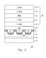
FIG. 1 (A) andFIG. 1(B) are diagrams schematically illustrating the conventional nitride LED structure formed on a SiC/Si substrate and on a SOI substrate according to the prior arts;FIG. 2 is a diagram schematically illustrating a group IV-based substrate having a patterned Group III nitride distributed Bragg reflector (DBR) multi-layer structure according to the present invention;FIG. 3 is a diagram schematically illustrating a Group III nitride LED structure formed on a group IV-based substrate according to an preferred embodiment of the present invention;FIG. 4 is an XRD diffraction diagram of the LED structure according toFIG. 3 ; andFIG. 5 is a Photoluminescence (PL) intensity diagram of the LED structure according toFIG. 3 at the temperature of 13 K.- The present invention will now be described more specifically with reference to the following embodiments. It is to be noted that the following descriptions of preferred embodiments of this invention are presented herein for purpose of illustration and description only; it is not intended to be exhaustive or to be limited to the precise form disclosed.
- Please refer to
FIG. 2 , which schematically shows a substrate structure having a patterned Group III nitride distributed Bragg reflector (DBR) multi-layer structure according to the present invention. As shown inFIG. 2 , thesubstrate structure 10 including a group IV-basedsubstrate 12, anucleation layer 14, anepitaxial layer 16 and a patterned distributed Bragg reflector (DBR)multi-layer structure 18. Typically, thenucleation layer 14 is an AlN diffusion barrier layer formed on the group IV-basedsubstrate 12 by a relatively low temperature growth process. Since the growth process is implemented in the relatively low temperature, the possible eutectic reaction between the Al element of the AlN diffusion barrier layer and the group IV element, such as silicon element, of the group IV-basedsubstrate 12 could be avoidable. Further, thenucleation layer 14 could also be used as a diffusion barrier layer barrier layer for preventing the silicon of the group IV-basedsubstrate 12 from further being diffused. After the formation of the AlN nucleation layer (or diffusion barrier layer)14, a patternedGaN epitaxial layer 16 is formed on thenucleation layer 14, and then a distributed Bragg reflector (DBR)multi-layer structure 18, which is made of the Group III nitride and has a pattern corresponding to the patterned GaN epitaxial layer, is formed on theepitaxial layer 16. - Please further refer to
FIG. 3 , after the formation of thesubstrate structure 10 having a patterned Group III nitride DBR multi-layer structure, as shown inFIG. 2 , anGaN buffer layer 20 is formed on thesubstrate structure 10 through a lateral growth process. Then, an LEDactive layer 30 is formed on theGaN buffer layer 20, so that a light emitting device (LED)structure 100 formed on the Group IV-basedsubstrate structure 10 having a distributed Bragg reflector (DBR) multi-layer structure is provided. - As mentioned above, the distributed Bragg reflector (DBR)
multi-layer structure 18 of the present invention is preferably made of a material including a nitride of Group III material. The DBRmulti-layer structure 18 is not only used for reflecting the light emitting from the LEDactive layer 30, but also used as a barrier layer preventing the defect ofepitaxial layer 16 from being diffused upwardly. Accordingly, the DBRmulti-layer structure 18 could not only improve the optical property of the LED structure but also increase the light extraction efficiency of the LED structure. In a preferred embodiment of the present invention, the DBRmulti-layer structure 18 further has a reflective surface181 (as shown inFIG. 2 ) having a tilt angle τ with respect to a vertical. Typically, the light extraction efficiency of the LED structure could be affected by the tilt angle τ. Preferably, the tilt angle τ of thereflective surface 181 is ranged from 5 to 75 degree. In a preferred embodiment of the present invention, the light extraction efficiency of theLED structure 100 is optimal in a tilt angle τ of 64 degree with respect to a vertical line. - On the other hand, in a preferred embodiment of the present invention, the LED
active layer 30 of theLED structure 100 according to the present invention could include an n-type AlGaN layer 31 formed on theGaN buffer layer 20, an n-type GaN layer 32 formed on the n-type AlGaN layer 31, a multiple quantum wells (MQWs)active layer 33 formed on the n-type GaN layer 32, a p-type AlGaN layer 34 formed on the MQWsactive layer 33, and a p-type GaN layer 35 formed on the p-type AlGaN layer 34. - On the other hand, since the
GaN buffer layer 20 disposed between the LEDactive layer 30 and the Group IV-basedsubstrate structure 10 having a distributed Bragg reflector (DBR)multi-layer structure 18 is formed by a lateral growth process, there could be few stress accumulated within theGaN buffer layer 20. Accordingly, a better epitaxiy quality for theLED structure 100 could be obtained. Please refer toFIG. 4 , which shows an XRD diffraction diagram of the LED structure according toFIG. 3 . As shown inFIG. 4 , the peak value of theGaN buffer layer 20 occur at 34.57°, which means the stress within theGaN buffer layer 20 is released. - Further, please refer to
FIG. 5 , which further shows a Photoluminescence (PL) intensity diagram of the LED structure according toFIG. 3 at the temperature of 13 K. As shown inFIG. 5 , both the high peak value of the PL intensity and the smaller width of the full-width-half-maximum (FWHM) of the PL spectrum imply that a better epitaxy quality of theLED structure 100 is obtained. - While the invention has been described in terms of what is presently considered to be the most practical and preferred embodiments, it is to be understood that the invention needs not be limited to the disclosed embodiments. On the contrary, it is intended to cover various modifications and similar arrangements included within the spirit and scope of the appended claims, which are to be accorded with the broadest interpretation so as to encompass all such modifications and similar structures.
Claims (18)
Applications Claiming Priority (3)
| Application Number | Priority Date | Filing Date | Title |
|---|---|---|---|
| TW97117321 | 2008-05-09 | ||
| TW97117321A | 2008-05-09 | ||
| TW097117321ATWI362769B (en) | 2008-05-09 | 2008-05-09 | Light emitting device and fabrication method therefor |
Publications (2)
| Publication Number | Publication Date |
|---|---|
| US20090278165A1true US20090278165A1 (en) | 2009-11-12 |
| US7977687B2 US7977687B2 (en) | 2011-07-12 |
Family
ID=41266154
Family Applications (1)
| Application Number | Title | Priority Date | Filing Date |
|---|---|---|---|
| US12/291,396Expired - Fee RelatedUS7977687B2 (en) | 2008-05-09 | 2008-11-07 | Light emitter device |
Country Status (2)
| Country | Link |
|---|---|
| US (1) | US7977687B2 (en) |
| TW (1) | TWI362769B (en) |
Cited By (7)
| Publication number | Priority date | Publication date | Assignee | Title |
|---|---|---|---|---|
| US20120080698A1 (en)* | 2010-10-05 | 2012-04-05 | Taiwan Semiconductor Manufacturing Company, Ltd. | High efficiency light emitting diodes |
| US20120138947A1 (en)* | 2010-12-03 | 2012-06-07 | Aqualite Co., Ltd. | Epitaxial Structure With An Epitaxial Defect Barrier Layer And Methods Making The Same |
| CN102738332A (en)* | 2011-04-13 | 2012-10-17 | 展晶科技(深圳)有限公司 | Light emitting diode epitaxial structure and manufacture method thereof |
| US20140131727A1 (en)* | 2012-11-12 | 2014-05-15 | Advanced Optoelectronic Technology, Inc. | Light emitting diode chip and method for manufacturing the same |
| US9923050B2 (en) | 2013-09-24 | 2018-03-20 | Siltronic Ag | Semiconductor wafer and a method for producing the semiconductor wafer |
| US20180097137A1 (en)* | 2016-10-05 | 2018-04-05 | International Business Machines Corporation | High voltage photovoltaics |
| CN113809206A (en)* | 2020-06-11 | 2021-12-17 | 苏州晶湛半导体有限公司 | Semiconductor structure and method of making the same |
Families Citing this family (1)
| Publication number | Priority date | Publication date | Assignee | Title |
|---|---|---|---|---|
| US9705030B2 (en) | 2012-04-18 | 2017-07-11 | Technische Universität Berlin | UV LED with tunnel-injection layer |
Citations (97)
| Publication number | Priority date | Publication date | Assignee | Title |
|---|---|---|---|---|
| US3566215A (en)* | 1967-08-04 | 1971-02-23 | Siemens Ag | Tensioned semiconductor component |
| US3655439A (en)* | 1968-06-19 | 1972-04-11 | Siemens Ag | Method of producing thin layer components with at least one insulating intermediate layer |
| US3658585A (en)* | 1969-03-18 | 1972-04-25 | Siemens Ag | Method of precipitating layers of semiconducting or insulating material from a flowing reaction gas or from a flowing dopant gas upon heated semiconductor crystals |
| US3793984A (en)* | 1971-11-24 | 1974-02-26 | Siemens Ag | Apparatus for the production of closed end tubes of semiconductor material |
| US3941647A (en)* | 1973-03-08 | 1976-03-02 | Siemens Aktiengesellschaft | Method of producing epitaxially semiconductor layers |
| US3948693A (en)* | 1973-07-27 | 1976-04-06 | Siemens Aktiengesellschaft | Process for the production of yellow glowing gallium phosphide diodes |
| US4133702A (en)* | 1976-09-22 | 1979-01-09 | Siemens Aktiengesellschaft | Method of producing structured layers on a substrate being irradiated with two coherent particle beams |
| US4140546A (en)* | 1976-09-20 | 1979-02-20 | Siemens Aktiengesellschaft | Method of producing a monocrystalline layer on a substrate |
| US4261770A (en)* | 1979-03-19 | 1981-04-14 | Siemens Aktiengesellschaft | Process for producing epitaxial semiconductor material layers on monocrystalline substrates via liquid phase shift epitaxy |
| US4505765A (en)* | 1982-07-21 | 1985-03-19 | Siemens Aktiengesellschaft | Manufacturing method for a planar photodiode with hetero-structure |
| US4568206A (en)* | 1983-04-25 | 1986-02-04 | Nichia Seimitsu Kogyo Co., Ltd. | Retainer for ball bearing |
| US4656636A (en)* | 1984-10-03 | 1987-04-07 | Siemens Aktiengesellschaft | Method for manufacturing of integrated DFB laser with coupled strip waveguide on a substrate |
| US4661175A (en)* | 1984-06-07 | 1987-04-28 | Siemens Aktiengesellschaft | Method of making InGaAsP and InGaAs double hetero-structure lasers and LEDs |
| US4722088A (en)* | 1984-09-14 | 1988-01-26 | Siemens Aktiengesellschaft | Semiconductor laser for high optical output power with reduced mirror heating |
| US4740259A (en)* | 1985-09-13 | 1988-04-26 | Siemens Aktiengesellschaft | Method of making a light-emitting-diode (led) with spherical lens |
| US4818722A (en)* | 1986-09-29 | 1989-04-04 | Siemens Aktiengesellschaft | Method for generating a strip waveguide |
| US4904617A (en)* | 1987-09-17 | 1990-02-27 | Siemens Aktiengesellschaft | Method for separating monolithically produced laser diodes |
| US4904618A (en)* | 1988-08-22 | 1990-02-27 | Neumark Gertrude F | Process for doping crystals of wide band gap semiconductors |
| US4907044A (en)* | 1987-10-15 | 1990-03-06 | Siemens Aktiengesellschaft | Optical emission device |
| US4907534A (en)* | 1988-12-09 | 1990-03-13 | Siemens Aktiengesellschaft | Gas distributor for OMVPE Growth |
| US4911102A (en)* | 1987-01-31 | 1990-03-27 | Toyoda Gosei Co., Ltd. | Process of vapor growth of gallium nitride and its apparatus |
| US4918497A (en)* | 1988-12-14 | 1990-04-17 | Cree Research, Inc. | Blue light emitting diode formed in silicon carbide |
| US4982314A (en)* | 1988-12-09 | 1991-01-01 | Nichia Kagaku Kogyo K.K. | Power source circuit apparatus for electro-luminescence device |
| US4985742A (en)* | 1989-07-07 | 1991-01-15 | University Of Colorado Foundation, Inc. | High temperature semiconductor devices having at least one gallium nitride layer |
| US4987576A (en)* | 1988-11-30 | 1991-01-22 | Siemens Aktiengesellschaft | Electrically tunable semiconductor laser with ridge waveguide |
| US4990990A (en)* | 1987-04-07 | 1991-02-05 | Siemens Aktiengesellschaft | Monolithically integrated waveguide-photodiode-FET combination |
| US4990466A (en)* | 1988-11-01 | 1991-02-05 | Siemens Corporate Research, Inc. | Method for fabricating index-guided semiconductor laser |
| US5005057A (en)* | 1989-04-28 | 1991-04-02 | Kabushiki Kaisha Toshiba | Semiconductor light-emitting diode and method of manufacturing the same |
| US5006908A (en)* | 1989-02-13 | 1991-04-09 | Nippon Telegraph And Telephone Corporation | Epitaxial Wurtzite growth structure for semiconductor light-emitting device |
| US5008735A (en)* | 1989-12-07 | 1991-04-16 | General Instrument Corporation | Packaged diode for high temperature operation |
| US5008789A (en)* | 1989-02-22 | 1991-04-16 | Nichia Kagaku Kogyo K.K. | Fluorescent lamp having ultraviolet reflecting layer |
| US5093576A (en)* | 1991-03-15 | 1992-03-03 | Cree Research | High sensitivity ultraviolet radiation detector |
| US5182670A (en)* | 1991-08-30 | 1993-01-26 | Apa Optics, Inc. | Narrow band algan filter |
| US5184247A (en)* | 1989-07-17 | 1993-02-02 | Siemens Aktiengesellschaft | Optically stabilized feedback amplifier |
| US5185207A (en)* | 1990-08-12 | 1993-02-09 | Nichia Kagaku Kogyo K.K. | Phosphor for cathode ray tube and surface treatment method for the phosphor |
| US5200022A (en)* | 1990-10-03 | 1993-04-06 | Cree Research, Inc. | Method of improving mechanically prepared substrate surfaces of alpha silicon carbide for deposition of beta silicon carbide thereon and resulting product |
| US5202777A (en)* | 1991-05-31 | 1993-04-13 | Hughes Aircraft Company | Liquid crystal light value in combination with cathode ray tube containing a far-red emitting phosphor |
| US5205905A (en)* | 1990-05-30 | 1993-04-27 | Toyoda Gosei Co., Ltd. | Dry etching method for semiconductor |
| US5278433A (en)* | 1990-02-28 | 1994-01-11 | Toyoda Gosei Co., Ltd. | Light-emitting semiconductor device using gallium nitride group compound with double layer structures for the n-layer and/or the i-layer |
| US5281830A (en)* | 1990-10-27 | 1994-01-25 | Toyoda Gosei Co., Ltd. | Light-emitting semiconductor device using gallium nitride group compound |
| US5290393A (en)* | 1991-01-31 | 1994-03-01 | Nichia Kagaku Kogyo K.K. | Crystal growth method for gallium nitride-based compound semiconductor |
| US5306662A (en)* | 1991-11-08 | 1994-04-26 | Nichia Chemical Industries, Ltd. | Method of manufacturing P-type compound semiconductor |
| US5381103A (en)* | 1992-10-13 | 1995-01-10 | Cree Research, Inc. | System and method for accelerated degradation testing of semiconductor devices |
| US5382822A (en)* | 1992-09-25 | 1995-01-17 | Siemens Aktiengesellschaft | Metal-insulator semiconductor field-effect transistor |
| US5389571A (en)* | 1991-12-18 | 1995-02-14 | Hiroshi Amano | Method of fabricating a gallium nitride based semiconductor device with an aluminum and nitrogen containing intermediate layer |
| US5390210A (en)* | 1993-11-22 | 1995-02-14 | Hewlett-Packard Company | Semiconductor laser that generates second harmonic light with attached nonlinear crystal |
| US5394005A (en)* | 1992-05-05 | 1995-02-28 | General Electric Company | Silicon carbide photodiode with improved short wavelength response and very low leakage current |
| US5393993A (en)* | 1993-12-13 | 1995-02-28 | Cree Research, Inc. | Buffer structure between silicon carbide and gallium nitride and resulting semiconductor devices |
| US5404282A (en)* | 1993-09-17 | 1995-04-04 | Hewlett-Packard Company | Multiple light emitting diode module |
| US5408120A (en)* | 1992-07-23 | 1995-04-18 | Toyoda Gosei Co., Ltd. | Light-emitting device of gallium nitride compound semiconductor |
| US5409859A (en)* | 1992-09-10 | 1995-04-25 | Cree Research, Inc. | Method of forming platinum ohmic contact to p-type silicon carbide |
| US5497012A (en)* | 1994-06-15 | 1996-03-05 | Hewlett-Packard Company | Unipolar band minima devices |
| US5502316A (en)* | 1993-03-19 | 1996-03-26 | Hewlett-Packard Company | Wafer bonding of light emitting diode layers |
| US5506421A (en)* | 1992-11-24 | 1996-04-09 | Cree Research, Inc. | Power MOSFET in silicon carbide |
| US5511084A (en)* | 1994-01-19 | 1996-04-23 | Siemens Aktiengesellschaft | Tunable laser diode |
| US5592501A (en)* | 1994-09-20 | 1997-01-07 | Cree Research, Inc. | Low-strain laser structures with group III nitride active layers |
| US5592578A (en)* | 1995-11-01 | 1997-01-07 | Hewlett-Packard Company | Peripheral optical element for redirecting light from an LED |
| US5596595A (en)* | 1995-06-08 | 1997-01-21 | Hewlett-Packard Company | Current and heat spreading transparent layers for surface-emitting lasers |
| US5604135A (en)* | 1994-08-12 | 1997-02-18 | Cree Research, Inc. | Method of forming green light emitting diode in silicon carbide |
| US5604763A (en)* | 1994-04-20 | 1997-02-18 | Toyoda Gosei Co., Ltd. | Group III nitride compound semiconductor laser diode and method for producing same |
| US5612260A (en)* | 1992-06-05 | 1997-03-18 | Cree Research, Inc. | Method of obtaining high quality silicon dioxide passivation on silicon carbide and resulting passivated structures |
| US5614736A (en)* | 1992-08-28 | 1997-03-25 | Siemens Aktiengesellschaft | Gallium phosphate light emitting diode with zinc-doped contact |
| US5616177A (en)* | 1994-02-23 | 1997-04-01 | Hewlett-Packard Company | Group II-VI semiconductor laser and method for the manufacture thereof |
| US5621749A (en)* | 1995-09-06 | 1997-04-15 | Hewlett-Packard Company | Praseodymium-doped fluoride fiber upconversion laser for the generation of blue light |
| US5620557A (en)* | 1993-12-27 | 1997-04-15 | Toyoda Gosei Co., Ltd. | Sapphireless group III nitride semiconductor and method for making same |
| US5625202A (en)* | 1995-06-08 | 1997-04-29 | University Of Central Florida | Modified wurtzite structure oxide compounds as substrates for III-V nitride compound semiconductor epitaxial thin film growth |
| US5707139A (en)* | 1995-11-01 | 1998-01-13 | Hewlett-Packard Company | Vertical cavity surface emitting laser arrays for illumination |
| US5718760A (en)* | 1996-02-05 | 1998-02-17 | Cree Research, Inc. | Growth of colorless silicon carbide crystals |
| US5719409A (en)* | 1996-06-06 | 1998-02-17 | Cree Research, Inc. | Silicon carbide metal-insulator semiconductor field effect transistor |
| US5724373A (en)* | 1996-11-15 | 1998-03-03 | Hewlett-Packard Company | Microphotonic acousto-optic tunable laser |
| US5724062A (en)* | 1992-08-05 | 1998-03-03 | Cree Research, Inc. | High resolution, high brightness light emitting diode display and method and producing the same |
| US5724376A (en)* | 1995-11-30 | 1998-03-03 | Hewlett-Packard Company | Transparent substrate vertical cavity surface emitting lasers fabricated by semiconductor wafer bonding |
| US5727014A (en)* | 1995-10-31 | 1998-03-10 | Hewlett-Packard Company | Vertical-cavity surface-emitting laser generating light with a defined direction of polarization |
| US5729029A (en)* | 1996-09-06 | 1998-03-17 | Hewlett-Packard Company | Maximizing electrical doping while reducing material cracking in III-V nitride semiconductor devices |
| US5729567A (en)* | 1995-04-28 | 1998-03-17 | Hewlett-Packard Company | Multilayer film structure and vertical cavity surface emitting lasers |
| US5734182A (en)* | 1992-11-20 | 1998-03-31 | Nichia Chemical Industries Ltd. | Light-emitting gallium nitride-based compound semiconducor device |
| US5733796A (en)* | 1990-02-28 | 1998-03-31 | Toyoda Gosei Co., Ltd. | Light-emitting semiconductor device using gallium nitride group compound |
| US5739552A (en)* | 1994-10-24 | 1998-04-14 | Mitsubishi Denki Kabushiki Kaisha | Semiconductor light emitting diode producing visible light |
| US5739554A (en)* | 1995-05-08 | 1998-04-14 | Cree Research, Inc. | Double heterojunction light emitting diode with gallium nitride active layer |
| US5742133A (en)* | 1995-09-07 | 1998-04-21 | Siemens Aktiengesellschaft | Driver circuit for an led |
| US5741431A (en)* | 1997-05-15 | 1998-04-21 | Industrial Technology Research Institute | Laser assisted cryoetching |
| US5741724A (en)* | 1996-12-27 | 1998-04-21 | Motorola | Method of growing gallium nitride on a spinel substrate |
| US5855924A (en)* | 1995-12-27 | 1999-01-05 | Siemens Microelectronics, Inc. | Closed-mold for LED alphanumeric displays |
| US5859496A (en)* | 1995-05-29 | 1999-01-12 | Nichia Chemical Industries, Ltd. | Lamp containing long decay phosphor |
| US5858277A (en)* | 1992-12-23 | 1999-01-12 | Osram Sylvania Inc. | Aqueous phosphor coating suspension for lamps |
| US5862167A (en)* | 1994-07-19 | 1999-01-19 | Toyoda Gosei Co., Ltd. | Light-emitting semiconductor device using gallium nitride compound |
| US5861713A (en)* | 1996-06-26 | 1999-01-19 | Nec Corporation | Low voltage electron beam display apparatus having brightness increased by reducing an oxide inevitably formed on a surface of an oxisulfide phosphor on manufacture |
| US5861190A (en)* | 1996-03-25 | 1999-01-19 | Hewlett-Packard Co. | Arrangement for growing a thin dielectric layer on a semiconductor wafer at low temperatures |
| US5867516A (en)* | 1996-03-12 | 1999-02-02 | Hewlett-Packard Company | Vertical cavity surface emitting laser with reduced turn-on jitter and increased single-mode output |
| US5868837A (en)* | 1997-01-17 | 1999-02-09 | Cornell Research Foundation, Inc. | Low temperature method of preparing GaN single crystals |
| US5877558A (en)* | 1993-04-28 | 1999-03-02 | Nichia Chemical Industries, Ltd. | Gallium nitride-based III-V group compound semiconductor |
| US5879588A (en)* | 1997-09-24 | 1999-03-09 | Osram Sylvania Inc. | Terbium-activated gadolinium oxysulfide phosphor with reduced blue emission |
| US5879587A (en)* | 1997-09-24 | 1999-03-09 | Osram Sylvania Inc. | Terbium-activated rare earth oxysulfide phosphor with enhanced green:blue emission ratio |
| US5889806A (en)* | 1996-08-08 | 1999-03-30 | Toyoda Gosei Co., Ltd. | Group III nitride compound semiconductor laser diodes |
| US5889802A (en)* | 1994-10-22 | 1999-03-30 | Hewlett-Packard Company | Bias controller and method |
| US20050040413A1 (en)* | 2001-03-27 | 2005-02-24 | Takashi Takahashi | Semiconductor light-emitting device, surface-emission laser diode, and production apparatus thereof, production method, optical module and optical telecommunication system |
| US20050067625A1 (en)* | 2003-09-29 | 2005-03-31 | Sanyo Electric Co., Ltd. | Semiconductor light-emitting device |
Family Cites Families (227)
| Publication number | Priority date | Publication date | Assignee | Title |
|---|---|---|---|---|
| NL6405927A (en) | 1963-06-07 | 1964-12-08 | ||
| DE1789061A1 (en) | 1968-09-30 | 1971-12-23 | Siemens Ag | Laser diode |
| US4020791A (en) | 1969-06-30 | 1977-05-03 | Siemens Aktiengesellschaft | Apparatus for indiffusing dopants into semiconductor material |
| US4404265A (en) | 1969-10-01 | 1983-09-13 | Rockwell International Corporation | Epitaxial composite and method of making |
| US3853974A (en) | 1970-04-06 | 1974-12-10 | Siemens Ag | Method of producing a hollow body of semiconductor material |
| DE2033444C3 (en) | 1970-07-06 | 1979-02-15 | Siemens Ag | Device for diffusing dopants into wafers made of semiconductor material |
| FR2110317B1 (en) | 1970-10-09 | 1975-04-18 | Siemens Ag | |
| DE2125085C3 (en) | 1971-05-19 | 1979-02-22 | Siemens Ag, 1000 Berlin Und 8000 Muenchen | Device for manufacturing tubes closed on one side from semiconductor material |
| US3819974A (en) | 1973-03-12 | 1974-06-25 | D Stevenson | Gallium nitride metal-semiconductor junction light emitting diode |
| DE2340225A1 (en) | 1973-08-08 | 1975-02-20 | Siemens Ag | METHOD FOR MANUFACTURING DIRECT HEATABLE HOLLOW BODIES FROM SEMICONDUCTOR MATERIAL |
| IE39673B1 (en) | 1973-10-02 | 1978-12-06 | Siemens Ag | Improvements in or relating to semiconductor luminescence diodes |
| FR2251104B1 (en) | 1973-11-14 | 1978-08-18 | Siemens Ag | |
| US4062035A (en) | 1975-02-05 | 1977-12-06 | Siemens Aktiengesellschaft | Luminescent diode |
| DE2528192C3 (en) | 1975-06-24 | 1979-02-01 | Siemens Ag, 1000 Berlin Und 8000 Muenchen | Device for depositing elemental silicon on a rod-shaped support body made of elemental silicon |
| US4098223A (en) | 1976-05-03 | 1978-07-04 | Siemens Aktiengesellschaft | Apparatus for heat treating semiconductor wafers |
| US4108539A (en) | 1976-11-18 | 1978-08-22 | Hewlett-Packard Company | Reflecting lens system |
| US4113381A (en) | 1976-11-18 | 1978-09-12 | Hewlett-Packard Company | Surveying instrument and method |
| DE2716143A1 (en) | 1977-04-12 | 1978-10-19 | Siemens Ag | LIGHT-EMITTING SEMI-CONDUCTOR COMPONENT |
| US4154625A (en) | 1977-11-16 | 1979-05-15 | Bell Telephone Laboratories, Incorporated | Annealing of uncapped compound semiconductor materials by pulsed energy deposition |
| DE3003285A1 (en) | 1980-01-30 | 1981-08-06 | Siemens AG, 1000 Berlin und 8000 München | METHOD FOR PRODUCING LOW-RESISTANT, SINGLE-CRYSTAL METAL OR ALLOY LAYERS ON SUBSTRATES |
| DE3016778A1 (en) | 1980-04-30 | 1981-11-05 | Siemens AG, 1000 Berlin und 8000 München | LASER DIODE |
| US4423349A (en) | 1980-07-16 | 1983-12-27 | Nichia Denshi Kagaku Co., Ltd. | Green fluorescence-emitting material and a fluorescent lamp provided therewith |
| DE3208638A1 (en) | 1982-03-10 | 1983-09-22 | Siemens AG, 1000 Berlin und 8000 München | SILICON CARBIDE LUMINESCENCE DIODE |
| JPS58158972A (en) | 1982-03-16 | 1983-09-21 | Toshiba Corp | Manufacturing method of semiconductor device |
| DE3210086A1 (en) | 1982-03-19 | 1983-09-22 | Siemens AG, 1000 Berlin und 8000 München | LUMINESCENCE DIODE, SUITABLE AS PRESSURE SENSOR |
| DE3328902A1 (en) | 1983-08-10 | 1985-02-28 | Siemens AG, 1000 Berlin und 8000 München | DISPLAY WITH A NUMBER OF LIGHT-EMITTING SEMICONDUCTOR COMPONENTS |
| DE3338335A1 (en) | 1983-10-21 | 1985-05-09 | Siemens AG, 1000 Berlin und 8000 München | METHOD FOR PRODUCING LARGE-SIDED SILICON CRYSTAL BODIES FOR SOLAR CELLS |
| DE3413667A1 (en) | 1984-04-11 | 1985-10-17 | Siemens AG, 1000 Berlin und 8000 München | METHOD FOR ADJUSTING A COUPLING OPTICS PROVIDED AT THE END OF AN OPTICAL WAVE GUIDE TO A SEMICONDUCTOR LASER, AND DEVICE FOR CARRYING OUT THE METHOD |
| US4599244A (en) | 1984-07-11 | 1986-07-08 | Siemens Aktiengesellschaft | Method large-area silicon bodies |
| DE3434741A1 (en) | 1984-09-21 | 1986-04-03 | Siemens AG, 1000 Berlin und 8000 München | COUPLED LASER DIODE ARRANGEMENT |
| DE3435148A1 (en) | 1984-09-25 | 1986-04-03 | Siemens AG, 1000 Berlin und 8000 München | LASER DIODE WITH BURNED ACTIVE LAYER AND WITH LATERAL CURRENT LIMITATION BY SELF-ADJUSTED PN TRANSITION AND METHOD FOR PRODUCING SUCH A LASER DIODE |
| US4683574A (en) | 1984-09-26 | 1987-07-28 | Siemens Aktiengesellschaft | Semiconductor laser diode with buried hetero-structure |
| US4615766A (en) | 1985-02-27 | 1986-10-07 | International Business Machines Corporation | Silicon cap for annealing gallium arsenide |
| DE3610333A1 (en) | 1985-04-19 | 1986-11-27 | Siemens AG, 1000 Berlin und 8000 München | Method for producing a surface grating (lattice, grid) having a specific grating constant on a lower-lying surface region of a mesastructure |
| US5250366A (en) | 1985-05-18 | 1993-10-05 | Nichia Kagaku Kogyo K.K. | Phosphor which emits light by the excitation of X-ray, and a X-ray intensifying screen using the phosphor |
| JPS62246988A (en) | 1986-04-18 | 1987-10-28 | Nichia Chem Ind Ltd | X-ray phosphor and x-ray sensitized paper |
| US4959174A (en) | 1985-05-18 | 1990-09-25 | Nichia Kagaku Kogyo K.K. | Phosphor which emits light by the excitation of X-ray |
| DE3531734A1 (en) | 1985-09-05 | 1987-03-12 | Siemens Ag | DEVICE FOR POSITIONING A SEMICONDUCTOR LASER WITH SELF-ADJUSTING EFFECT FOR A FIBER TO BE COUPLED |
| DE3534017A1 (en) | 1985-09-24 | 1987-03-26 | Siemens Ag | METHOD FOR COUPLING A LASER DIODE TO A MONOMODE LIGHT WAVE GUIDE, AND AN ARRANGEMENT OF A LASER DIODE AND A LIGHT WAVE GUIDE COUPLED TO IT |
| EP0236713A3 (en) | 1986-02-10 | 1988-06-29 | Siemens Aktiengesellschaft | Laser diode |
| EP0237812A3 (en) | 1986-03-20 | 1988-06-29 | Siemens Aktiengesellschaft | Semiconductor laser array with a collimated beam |
| DE3611167A1 (en) | 1986-04-03 | 1987-10-08 | Siemens Ag | ARRAY WITH COUPLED OPTICAL WAVE GUIDES |
| JPH0662943B2 (en) | 1986-10-06 | 1994-08-17 | 日亜化学工業株式会社 | Fluorescent material for radiographic intensifying screen |
| US5218216A (en) | 1987-01-31 | 1993-06-08 | Toyoda Gosei Co., Ltd. | Gallium nitride group semiconductor and light emitting diode comprising it and the process of producing the same |
| JPS63224252A (en) | 1987-02-06 | 1988-09-19 | シーメンス、アクチエンゲゼルシヤフト | Waveguide-photodiode array |
| JPH01209776A (en) | 1987-02-20 | 1989-08-23 | Siemens Ag | Laser transmitting apparatus |
| JPH0630242B2 (en) | 1987-03-04 | 1994-04-20 | 陽一 峰松 | Ultraviolet fluorescent lamps for artificial accelerated exposure testing of polymeric materials |
| DE3810245A1 (en) | 1987-03-27 | 1988-10-06 | Japan Incubator Inc | LIGHT-EMITTING ELEMENT AND METHOD FOR THE PRODUCTION THEREOF |
| US4855118A (en) | 1987-04-15 | 1989-08-08 | Nichia Kagaku Kogyo K.K. | Method of producing fluorapatite |
| JPH0774333B2 (en) | 1987-06-29 | 1995-08-09 | 日亜化学工業株式会社 | Luminescent composition |
| DE3727546A1 (en) | 1987-08-18 | 1989-03-02 | Siemens Ag | LIGHT AMPLIFIER WITH RING-SHAPED RADIATION, IN PARTICULAR RING LASER DIODE |
| EP0309744A3 (en) | 1987-09-29 | 1989-06-28 | Siemens Aktiengesellschaft | Arrangement with a thin-film waveguide extending in a flat manner |
| US4960728A (en) | 1987-10-05 | 1990-10-02 | Texas Instruments Incorporated | Homogenization anneal of II-VI compounds |
| US4945394A (en) | 1987-10-26 | 1990-07-31 | North Carolina State University | Bipolar junction transistor on silicon carbide |
| US4947218A (en) | 1987-11-03 | 1990-08-07 | North Carolina State University | P-N junction diodes in silicon carbide |
| GB2212658B (en) | 1987-11-13 | 1992-02-12 | Plessey Co Plc | Solid state light source |
| JP2663483B2 (en) | 1988-02-29 | 1997-10-15 | 勝 西川 | Method of forming resist pattern |
| EP0331778B1 (en) | 1988-03-09 | 1992-01-15 | Hewlett-Packard GmbH | Output amplifier |
| US4864369A (en) | 1988-07-05 | 1989-09-05 | Hewlett-Packard Company | P-side up double heterojunction AlGaAs light-emitting diode |
| US5252499A (en) | 1988-08-15 | 1993-10-12 | Rothschild G F Neumark | Wide band-gap semiconductors having low bipolar resistivity and method of formation |
| EP0356059B1 (en) | 1988-08-15 | 2000-01-26 | Gertrude F. Neumark | Process for doping crystals of wide band gap semiconductors |
| DE3836802A1 (en) | 1988-10-28 | 1990-05-03 | Siemens Ag | SEMICONDUCTOR LASER ARRANGEMENT FOR HIGH OUTPUT PERFORMANCE IN LATERAL BASIC MODE |
| DE3838016A1 (en) | 1988-11-09 | 1990-05-10 | Siemens Ag | SEMICONDUCTOR LASER IN THE GAA1INAS SYSTEM |
| US5027168A (en) | 1988-12-14 | 1991-06-25 | Cree Research, Inc. | Blue light emitting diode formed in silicon carbide |
| US5061972A (en) | 1988-12-14 | 1991-10-29 | Cree Research, Inc. | Fast recovery high temperature rectifying diode formed in silicon carbide |
| CA2008176A1 (en) | 1989-01-25 | 1990-07-25 | John W. Palmour | Silicon carbide schottky diode and method of making same |
| JP3026087B2 (en) | 1989-03-01 | 2000-03-27 | 豊田合成株式会社 | Gas phase growth method of gallium nitride based compound semiconductor |
| DE59009909D1 (en) | 1989-04-19 | 1996-01-11 | Siemens Ag | Device with a crucible in an effusion cell of a molecular beam epitaxy system. |
| US5160492A (en) | 1989-04-24 | 1992-11-03 | Hewlett-Packard Company | Buried isolation using ion implantation and subsequent epitaxial growth |
| JP2809691B2 (en) | 1989-04-28 | 1998-10-15 | 株式会社東芝 | Semiconductor laser |
| US5049779A (en) | 1989-05-02 | 1991-09-17 | Nichia Kagaku Kogyo K.K. | Phosphor composition used for fluorescent lamp and fluorescent lamp using the same |
| EP0405214A3 (en) | 1989-06-27 | 1991-06-05 | Siemens Aktiengesellschaft | Pin-fet combination with buried p-type layer |
| US5119540A (en) | 1990-07-24 | 1992-06-09 | Cree Research, Inc. | Apparatus for eliminating residual nitrogen contamination in epitaxial layers of silicon carbide and resulting product |
| JPH07116429B2 (en) | 1989-08-25 | 1995-12-13 | 日亜化学工業株式会社 | Pigmented phosphor |
| US4966862A (en) | 1989-08-28 | 1990-10-30 | Cree Research, Inc. | Method of production of light emitting diodes |
| US4946547A (en) | 1989-10-13 | 1990-08-07 | Cree Research, Inc. | Method of preparing silicon carbide surfaces for crystal growth |
| US5366834A (en) | 1989-11-15 | 1994-11-22 | Nichia Kagaku Kogyo K.K. | Method of manufacturing a cathode ray tube phosphor screen |
| US5019746A (en) | 1989-12-04 | 1991-05-28 | Hewlett-Packard Company | Prefabricated wire leadframe for optoelectronic devices |
| US5077145A (en) | 1989-12-26 | 1991-12-31 | Nichia Kagaku Kogyo K.K. | Phosphor for x-ray intensifying screen and x-ray intensifying screen |
| US5210051A (en) | 1990-03-27 | 1993-05-11 | Cree Research, Inc. | High efficiency light emitting diodes from bipolar gallium nitride |
| JPH075883B2 (en) | 1990-04-21 | 1995-01-25 | 日亜化学工業株式会社 | Regeneration method of phosphor |
| DE59008666D1 (en) | 1990-05-28 | 1995-04-13 | Siemens Ag | Optoelectronic circuit. |
| JP2784255B2 (en) | 1990-10-02 | 1998-08-06 | 日亜化学工業株式会社 | Phosphor and discharge lamp using the same |
| EP0479298B1 (en) | 1990-10-02 | 1995-08-02 | Nichia Kagaku Kogyo K.K. | Phosphor composition, phosphor-coating composition, discharge lamp, and preparation method thereof |
| US5334277A (en) | 1990-10-25 | 1994-08-02 | Nichia Kagaky Kogyo K.K. | Method of vapor-growing semiconductor crystal and apparatus for vapor-growing the same |
| US5433169A (en) | 1990-10-25 | 1995-07-18 | Nichia Chemical Industries, Ltd. | Method of depositing a gallium nitride-based III-V group compound semiconductor crystal layer |
| US5208878A (en) | 1990-11-28 | 1993-05-04 | Siemens Aktiengesellschaft | Monolithically integrated laser-diode-waveguide combination |
| US5155062A (en) | 1990-12-20 | 1992-10-13 | Cree Research, Inc. | Method for silicon carbide chemical vapor deposition using levitated wafer system |
| JP3160914B2 (en) | 1990-12-26 | 2001-04-25 | 豊田合成株式会社 | Gallium nitride based compound semiconductor laser diode |
| US5146465A (en) | 1991-02-01 | 1992-09-08 | Apa Optics, Inc. | Aluminum gallium nitride laser |
| JP2786952B2 (en) | 1991-02-27 | 1998-08-13 | 株式会社豊田中央研究所 | Gallium nitride based compound semiconductor light emitting device and method of manufacturing the same |
| US5270554A (en) | 1991-06-14 | 1993-12-14 | Cree Research, Inc. | High power high frequency metal-semiconductor field-effect transistor formed in silicon carbide |
| US5264713A (en) | 1991-06-14 | 1993-11-23 | Cree Research, Inc. | Junction field-effect transistor formed in silicon carbide |
| US5164798A (en) | 1991-07-05 | 1992-11-17 | Hewlett-Packard Company | Diffusion control of P-N junction location in multilayer heterostructure light emitting devices |
| US5260960A (en) | 1991-07-26 | 1993-11-09 | Siemens Aktiengesellschaft | Tunable semiconductor laser on a semi-insulating substrate |
| US5467291A (en) | 1991-09-09 | 1995-11-14 | Hewlett-Packard Company | Measurement-based system for modeling and simulation of active semiconductor devices over an extended operating frequency range |
| JP2666228B2 (en) | 1991-10-30 | 1997-10-22 | 豊田合成株式会社 | Gallium nitride based compound semiconductor light emitting device |
| US5465249A (en) | 1991-11-26 | 1995-11-07 | Cree Research, Inc. | Nonvolatile random access memory device having transistor and capacitor made in silicon carbide substrate |
| JP2770629B2 (en) | 1991-12-26 | 1998-07-02 | 日亜化学工業株式会社 | Phosphor for cathode ray tube and surface treatment method thereof |
| US5233204A (en) | 1992-01-10 | 1993-08-03 | Hewlett-Packard Company | Light-emitting diode with a thick transparent layer |
| US5312560A (en) | 1992-03-19 | 1994-05-17 | Nichia Chemical Industries, Ltd. | Rare earth phosphor |
| EP0562143B1 (en) | 1992-03-27 | 1997-06-25 | Nichia Kagaku Kogyo K.K. | Solid-state image converting device |
| JP3244529B2 (en) | 1992-04-16 | 2002-01-07 | アジレント・テクノロジーズ・インク | Surface-emitting type second harmonic generation device |
| US5459107A (en) | 1992-06-05 | 1995-10-17 | Cree Research, Inc. | Method of obtaining high quality silicon dioxide passivation on silicon carbide and resulting passivated structures |
| US6344663B1 (en) | 1992-06-05 | 2002-02-05 | Cree, Inc. | Silicon carbide CMOS devices |
| US5252839A (en) | 1992-06-10 | 1993-10-12 | Hewlett-Packard Company | Superluminescent light-emitting diode with reverse biased absorber |
| US5343316A (en) | 1992-06-30 | 1994-08-30 | Nichia Chemical Industries, Ltd. | Phosphor for use in a cathode-ray tube and display device using one |
| US5359345A (en) | 1992-08-05 | 1994-10-25 | Cree Research, Inc. | Shuttered and cycled light emitting diode display and method of producing the same |
| US5265792A (en) | 1992-08-20 | 1993-11-30 | Hewlett-Packard Company | Light source and technique for mounting light emitting diodes |
| JP2657743B2 (en) | 1992-10-29 | 1997-09-24 | 豊田合成株式会社 | Nitrogen-3 group element compound semiconductor light emitting device |
| US5687391A (en) | 1992-12-11 | 1997-11-11 | Vibrametrics, Inc. | Fault tolerant multipoint control and data collection system |
| JPH06264054A (en) | 1993-03-11 | 1994-09-20 | Nichia Chem Ind Ltd | Production of phosphor for cathode ray tube |
| JPH06326350A (en) | 1993-05-12 | 1994-11-25 | Nichia Chem Ind Ltd | Infrared ray-visible ray converting element |
| US5416342A (en) | 1993-06-23 | 1995-05-16 | Cree Research, Inc. | Blue light-emitting diode with high external quantum efficiency |
| US5539217A (en) | 1993-08-09 | 1996-07-23 | Cree Research, Inc. | Silicon carbide thyristor |
| US5338944A (en) | 1993-09-22 | 1994-08-16 | Cree Research, Inc. | Blue light-emitting diode with degenerate junction structure |
| US5363390A (en) | 1993-11-22 | 1994-11-08 | Hewlett-Packard Company | Semiconductor laser that generates second harmonic light by means of a nonlinear crystal in the laser cavity |
| US5846844A (en) | 1993-11-29 | 1998-12-08 | Toyoda Gosei Co., Ltd. | Method for producing group III nitride compound semiconductor substrates using ZnO release layers |
| US5433533A (en) | 1993-12-20 | 1995-07-18 | Nichia Precision Industry Co., Ltd. | Shield plate for bearing |
| TW289837B (en) | 1994-01-18 | 1996-11-01 | Hwelett Packard Co | |
| US5514627A (en) | 1994-01-24 | 1996-05-07 | Hewlett-Packard Company | Method and apparatus for improving the performance of light emitting diodes |
| US5656832A (en) | 1994-03-09 | 1997-08-12 | Kabushiki Kaisha Toshiba | Semiconductor heterojunction device with ALN buffer layer of 3nm-10nm average film thickness |
| US5923118A (en) | 1997-03-07 | 1999-07-13 | Osram Sylvania Inc. | Neon gas discharge lamp providing white light with improved phospher |
| JPH07263748A (en) | 1994-03-22 | 1995-10-13 | Toyoda Gosei Co Ltd | Group III nitride semiconductor light emitting device and manufacturing method thereof |
| JP2698796B2 (en) | 1994-04-20 | 1998-01-19 | 豊田合成株式会社 | Group III nitride semiconductor light emitting device |
| EP0678945B1 (en) | 1994-04-20 | 1998-07-08 | Toyoda Gosei Co., Ltd. | Gallium nitride group compound semiconductor laser diode and method of manufacturing the same |
| JP3426699B2 (en) | 1994-04-27 | 2003-07-14 | 住友化学工業株式会社 | Process for producing polymer comprising unsaturated carboxylic acid and derivative thereof |
| US5808592A (en) | 1994-04-28 | 1998-09-15 | Toyoda Gosei Co., Ltd. | Integrated light-emitting diode lamp and method of producing the same |
| US5376303A (en) | 1994-06-10 | 1994-12-27 | Nichia Chemical Industries, Ltd. | Long Decay phoaphors |
| JPH0832112A (en) | 1994-07-20 | 1996-02-02 | Toyoda Gosei Co Ltd | Group III nitride semiconductor light emitting device |
| US5650641A (en) | 1994-09-01 | 1997-07-22 | Toyoda Gosei Co., Ltd. | Semiconductor device having group III nitride compound and enabling control of emission color, and flat display comprising such device |
| EP0703649B1 (en) | 1994-09-14 | 2003-01-15 | Matsushita Electric Industrial Co., Ltd. | Method for stabilizing output of higher harmonic waves and short wavelength laser beam source using the same |
| US5686737A (en) | 1994-09-16 | 1997-11-11 | Cree Research, Inc. | Self-aligned field-effect transistor for high frequency applications |
| US5523589A (en) | 1994-09-20 | 1996-06-04 | Cree Research, Inc. | Vertical geometry light emitting diode with group III nitride active layer and extended lifetime |
| JP2666237B2 (en) | 1994-09-20 | 1997-10-22 | 豊田合成株式会社 | Group III nitride semiconductor light emitting device |
| US5631190A (en) | 1994-10-07 | 1997-05-20 | Cree Research, Inc. | Method for producing high efficiency light-emitting diodes and resulting diode structures |
| US5892784A (en) | 1994-10-27 | 1999-04-06 | Hewlett-Packard Company | N-drive p-common surface emitting laser fabricated on n+ substrate |
| US5892787A (en) | 1994-10-27 | 1999-04-06 | Hewlett-Packard Company | N-drive, p-common light-emitting devices fabricated on an n-type substrate and method of making same |
| US5491712A (en) | 1994-10-31 | 1996-02-13 | Lin; Hong | Integration of surface emitting laser and photodiode for monitoring power output of surface emitting laser |
| US5679153A (en) | 1994-11-30 | 1997-10-21 | Cree Research, Inc. | Method for reducing micropipe formation in the epitaxial growth of silicon carbide and resulting silicon carbide structures |
| US5777350A (en) | 1994-12-02 | 1998-07-07 | Nichia Chemical Industries, Ltd. | Nitride semiconductor light-emitting device |
| EP0800592B1 (en) | 1994-12-27 | 1998-08-26 | Siemens Aktiengesellschaft | Method of producing boron-doped monocrystalline silicon carbide |
| US5585648A (en) | 1995-02-03 | 1996-12-17 | Tischler; Michael A. | High brightness electroluminescent device, emitting in the green to ultraviolet spectrum, and method of making the same |
| US5661074A (en) | 1995-02-03 | 1997-08-26 | Advanced Technology Materials, Inc. | High brightness electroluminescent device emitting in the green to ultraviolet spectrum and method of making the same |
| DE19508222C1 (en) | 1995-03-08 | 1996-06-05 | Siemens Ag | Opto-electronic converter |
| JPH08264833A (en) | 1995-03-10 | 1996-10-11 | Hewlett Packard Co <Hp> | Light emitting diode |
| US5850410A (en) | 1995-03-16 | 1998-12-15 | Fujitsu Limited | Semiconductor laser and method for fabricating the same |
| EP0732754B1 (en) | 1995-03-17 | 2007-10-31 | Toyoda Gosei Co., Ltd. | Light-emitting semiconductor device using group III nitride compound |
| JP3773282B2 (en) | 1995-03-27 | 2006-05-10 | 豊田合成株式会社 | Method for forming electrode of gallium nitride compound semiconductor |
| DE19511593C2 (en) | 1995-03-29 | 1997-02-13 | Siemens Ag | Micro-optical device |
| US5670798A (en) | 1995-03-29 | 1997-09-23 | North Carolina State University | Integrated heterostructures of Group III-V nitride semiconductor materials including epitaxial ohmic contact non-nitride buffer layer and methods of fabricating same |
| US5659568A (en) | 1995-05-23 | 1997-08-19 | Hewlett-Packard Company | Low noise surface emitting laser for multimode optical link applications |
| TW304310B (en) | 1995-05-31 | 1997-05-01 | Siemens Ag | |
| JP2839077B2 (en) | 1995-06-15 | 1998-12-16 | 日本電気株式会社 | Gallium nitride based compound semiconductor light emitting device |
| US5785404A (en) | 1995-06-29 | 1998-07-28 | Siemens Microelectronics, Inc. | Localized illumination device |
| US5903016A (en) | 1995-06-30 | 1999-05-11 | Siemens Components, Inc. | Monolithic linear optocoupler |
| DE19524655A1 (en) | 1995-07-06 | 1997-01-09 | Huang Kuo Hsin | LED structure - has p=type aluminium gallium indium phosphide top cover layer on potential well structure and p=type window structure of respective thin and thick films on top layer |
| US5999552A (en) | 1995-07-19 | 1999-12-07 | Siemens Aktiengesellschaft | Radiation emitter component |
| DE19527536A1 (en) | 1995-07-27 | 1997-01-30 | Siemens Ag | Process for the production of silicon carbide single crystals |
| US5919422A (en) | 1995-07-28 | 1999-07-06 | Toyoda Gosei Co., Ltd. | Titanium dioxide photo-catalyzer |
| DE19629920B4 (en) | 1995-08-10 | 2006-02-02 | LumiLeds Lighting, U.S., LLC, San Jose | Light-emitting diode with a non-absorbing distributed Bragg reflector |
| US5900650A (en) | 1995-08-31 | 1999-05-04 | Kabushiki Kaisha Toshiba | Semiconductor device and method of manufacturing the same |
| DE19536463C2 (en) | 1995-09-29 | 2002-02-07 | Infineon Technologies Ag | Method of manufacturing a plurality of laser diode devices |
| DE19536438A1 (en) | 1995-09-29 | 1997-04-03 | Siemens Ag | Semiconductor device and manufacturing process |
| US5986317A (en) | 1995-09-29 | 1999-11-16 | Infineon Technologies Corporation | Optical semiconductor device having plural encapsulating layers |
| US5642375A (en) | 1995-10-26 | 1997-06-24 | Hewlett-Packard Company | Passively-locked external optical cavity |
| US5972801A (en) | 1995-11-08 | 1999-10-26 | Cree Research, Inc. | Process for reducing defects in oxide layers on silicon carbide |
| TW425722B (en) | 1995-11-27 | 2001-03-11 | Sumitomo Chemical Co | Group III-V compound semiconductor and light-emitting device |
| US5635146A (en) | 1995-11-30 | 1997-06-03 | Osram Sylvania Inc. | Method for the dissolution and purification of tantalum pentoxide |
| EP0781619A1 (en) | 1995-12-15 | 1997-07-02 | Cree Research, Inc. | Method of making silicone carbide wafers from silicon carbide bulk crystals |
| JP3409958B2 (en) | 1995-12-15 | 2003-05-26 | 株式会社東芝 | Semiconductor light emitting device |
| US5917202A (en) | 1995-12-21 | 1999-06-29 | Hewlett-Packard Company | Highly reflective contacts for light emitting semiconductor devices |
| FR2742926B1 (en) | 1995-12-22 | 1998-02-06 | Alsthom Cge Alcatel | METHOD AND DEVICE FOR PREPARING LASER FACES |
| US5991160A (en) | 1995-12-27 | 1999-11-23 | Infineon Technologies Corporation | Surface mount LED alphanumeric display |
| US5812105A (en) | 1996-06-10 | 1998-09-22 | Cree Research, Inc. | Led dot matrix drive method and apparatus |
| US5828684A (en) | 1995-12-29 | 1998-10-27 | Xerox Corporation | Dual polarization quantum well laser in the 200 to 600 nanometers range |
| DE19600306C1 (en) | 1996-01-05 | 1997-04-10 | Siemens Ag | Semiconductor component with hermetically-sealed housing for opto-electronic component |
| WO1997027629A1 (en) | 1996-01-24 | 1997-07-31 | Cree Research, Inc. | Mesa schottky diode with guard ring |
| US5923690A (en) | 1996-01-25 | 1999-07-13 | Matsushita Electric Industrial Co., Ltd. | Semiconductor laser device |
| US5761229A (en) | 1996-01-25 | 1998-06-02 | Hewlett-Packard Company | Integrated controlled intensity laser-based light source |
| US5835514A (en) | 1996-01-25 | 1998-11-10 | Hewlett-Packard Company | Laser-based controlled-intensity light source using reflection from a convex surface and method of making same |
| US5771254A (en) | 1996-01-25 | 1998-06-23 | Hewlett-Packard Company | Integrated controlled intensity laser-based light source |
| US5809050A (en) | 1996-01-25 | 1998-09-15 | Hewlett-Packard Company | Integrated controlled intensity laser-based light source using diffraction, scattering and transmission |
| US5811931A (en) | 1996-03-04 | 1998-09-22 | Hewlett Packard Company | Capped edge emitter |
| US5684623A (en) | 1996-03-20 | 1997-11-04 | Hewlett Packard Company | Narrow-band tunable optical source |
| US5779924A (en) | 1996-03-22 | 1998-07-14 | Hewlett-Packard Company | Ordered interface texturing for a light emitting device |
| JP3727106B2 (en) | 1996-04-17 | 2005-12-14 | 豊田合成株式会社 | Method of manufacturing group III nitride semiconductor laser diode |
| JP3209096B2 (en) | 1996-05-21 | 2001-09-17 | 豊田合成株式会社 | Group III nitride compound semiconductor light emitting device |
| DE19621124A1 (en) | 1996-05-24 | 1997-11-27 | Siemens Ag | Optoelectronic converter and its manufacturing process |
| KR100537349B1 (en) | 1996-06-26 | 2006-02-28 | 오스람 게젤샤프트 미트 베쉬랭크터 하프퉁 | Light-emitting semiconductor component with luminescence conversion element |
| DE19638667C2 (en) | 1996-09-20 | 2001-05-17 | Osram Opto Semiconductors Gmbh | Mixed-color light-emitting semiconductor component with luminescence conversion element |
| US5777433A (en) | 1996-07-11 | 1998-07-07 | Hewlett-Packard Company | High refractive index package material and a light emitting device encapsulated with such material |
| US5925898A (en) | 1996-07-18 | 1999-07-20 | Siemens Aktiengesellschaft | Optoelectronic transducer and production methods |
| US5818861A (en) | 1996-07-19 | 1998-10-06 | Hewlett-Packard Company | Vertical cavity surface emitting laser with low band gap highly doped contact layer |
| TW383508B (en) | 1996-07-29 | 2000-03-01 | Nichia Kagaku Kogyo Kk | Light emitting device and display |
| US5805624A (en) | 1996-07-30 | 1998-09-08 | Hewlett-Packard Company | Long-wavelength infra-red vertical cavity surface-emitting laser on a gallium arsenide substrate |
| DE59712346D1 (en) | 1996-09-19 | 2005-07-21 | Infineon Technologies Ag | Optical waveguide and method for its production |
| DE19645035C1 (en) | 1996-10-31 | 1998-04-30 | Siemens Ag | Multi-color light emitting image display device |
| US5835522A (en) | 1996-11-19 | 1998-11-10 | Hewlett-Packard Co. | Robust passively-locked optical cavity system |
| DE19649650B4 (en) | 1996-11-29 | 2005-02-24 | Siemens Ag | Surface-mountable radiation-emitting semiconductor component |
| US5966393A (en) | 1996-12-13 | 1999-10-12 | The Regents Of The University Of California | Hybrid light-emitting sources for efficient and cost effective white lighting and for full-color applications |
| DE19652548C1 (en) | 1996-12-17 | 1998-03-12 | Siemens Ag | Continuous epitaxy of nitrogen-containing semiconductor layers |
| DE19652528A1 (en) | 1996-12-17 | 1998-06-18 | Siemens Ag | LED with all-round light decoupling |
| US5838707A (en) | 1996-12-27 | 1998-11-17 | Motorola, Inc. | Ultraviolet/visible light emitting vertical cavity surface emitting laser and method of fabrication |
| JPH10215031A (en) | 1997-01-30 | 1998-08-11 | Hewlett Packard Co <Hp> | Semiconductor laser device |
| JPH10242074A (en) | 1997-02-21 | 1998-09-11 | Hewlett Packard Co <Hp> | Method for manufacturing nitride semiconductor device |
| TW353202B (en) | 1997-02-28 | 1999-02-21 | Hewlett Packard Co | Scribe and break of hard-to-scribe materials |
| SG63757A1 (en) | 1997-03-12 | 1999-03-30 | Hewlett Packard Co | Adding impurities to improve the efficiency of allngan quantum well led's |
| US6284016B1 (en) | 1997-03-21 | 2001-09-04 | Nippon Steel Corporation | Pressure converter steelmaking method |
| US6217662B1 (en) | 1997-03-24 | 2001-04-17 | Cree, Inc. | Susceptor designs for silicon carbide thin films |
| US5927995A (en) | 1997-04-09 | 1999-07-27 | Hewlett-Packard Company | Reduction of threading dislocations by amorphization and recrystallization |
| US5923946A (en) | 1997-04-17 | 1999-07-13 | Cree Research, Inc. | Recovery of surface-ready silicon carbide substrates |
| US6011279A (en) | 1997-04-30 | 2000-01-04 | Cree Research, Inc. | Silicon carbide field controlled bipolar switch |
| US6100586A (en) | 1997-05-23 | 2000-08-08 | Agilent Technologies, Inc. | Low voltage-drop electrical contact for gallium (aluminum, indium) nitride |
| US5969378A (en) | 1997-06-12 | 1999-10-19 | Cree Research, Inc. | Latch-up free power UMOS-bipolar transistor |
| US6121633A (en) | 1997-06-12 | 2000-09-19 | Cree Research, Inc. | Latch-up free power MOS-bipolar transistor |
| US5847507A (en) | 1997-07-14 | 1998-12-08 | Hewlett-Packard Company | Fluorescent dye added to epoxy of light emitting diode lens |
| KR100413792B1 (en)* | 1997-07-24 | 2004-02-14 | 삼성전자주식회사 | Short wavelength surface emitting laser device including dbr having stacked structure of gan layer and air layer and fabricating method thereof |
| CN1129192C (en) | 1997-08-29 | 2003-11-26 | 克里公司 | Robust group III nitride light emitting diode for high reliability in standard applications |
| US5958295A (en) | 1997-09-24 | 1999-09-28 | Osram Sylvania Inc. | Terbium-activated rare earth oxysulfide phosphor with enhanced blue emission |
| JP3955367B2 (en) | 1997-09-30 | 2007-08-08 | フィリップス ルミレッズ ライティング カンパニー リミテッド ライアビリティ カンパニー | Optical semiconductor device and manufacturing method thereof |
| US5972781A (en) | 1997-09-30 | 1999-10-26 | Siemens Aktiengesellschaft | Method for producing semiconductor chips |
| US6201262B1 (en) | 1997-10-07 | 2001-03-13 | Cree, Inc. | Group III nitride photonic devices on silicon carbide substrates with conductive buffer interlay structure |
| US5935705A (en) | 1997-10-15 | 1999-08-10 | National Science Council Of Republic Of China | Crystalline Six Cy Nz with a direct optical band gap of 3.8 eV |
| US5920766A (en) | 1998-01-07 | 1999-07-06 | Xerox Corporation | Red and blue stacked laser diode array by wafer fusion |
| US5959316A (en) | 1998-09-01 | 1999-09-28 | Hewlett-Packard Company | Multiple encapsulation of phosphor-LED devices |
| US6943377B2 (en)* | 2002-11-21 | 2005-09-13 | Sensor Electronic Technology, Inc. | Light emitting heterostructure |
- 2008
- 2008-05-09TWTW097117321Apatent/TWI362769B/ennot_activeIP Right Cessation
- 2008-11-07USUS12/291,396patent/US7977687B2/ennot_activeExpired - Fee Related
Patent Citations (99)
| Publication number | Priority date | Publication date | Assignee | Title |
|---|---|---|---|---|
| US3566215A (en)* | 1967-08-04 | 1971-02-23 | Siemens Ag | Tensioned semiconductor component |
| US3655439A (en)* | 1968-06-19 | 1972-04-11 | Siemens Ag | Method of producing thin layer components with at least one insulating intermediate layer |
| US3658585A (en)* | 1969-03-18 | 1972-04-25 | Siemens Ag | Method of precipitating layers of semiconducting or insulating material from a flowing reaction gas or from a flowing dopant gas upon heated semiconductor crystals |
| US3793984A (en)* | 1971-11-24 | 1974-02-26 | Siemens Ag | Apparatus for the production of closed end tubes of semiconductor material |
| US3941647A (en)* | 1973-03-08 | 1976-03-02 | Siemens Aktiengesellschaft | Method of producing epitaxially semiconductor layers |
| US3948693A (en)* | 1973-07-27 | 1976-04-06 | Siemens Aktiengesellschaft | Process for the production of yellow glowing gallium phosphide diodes |
| US4140546A (en)* | 1976-09-20 | 1979-02-20 | Siemens Aktiengesellschaft | Method of producing a monocrystalline layer on a substrate |
| US4133702A (en)* | 1976-09-22 | 1979-01-09 | Siemens Aktiengesellschaft | Method of producing structured layers on a substrate being irradiated with two coherent particle beams |
| US4261770A (en)* | 1979-03-19 | 1981-04-14 | Siemens Aktiengesellschaft | Process for producing epitaxial semiconductor material layers on monocrystalline substrates via liquid phase shift epitaxy |
| US4505765A (en)* | 1982-07-21 | 1985-03-19 | Siemens Aktiengesellschaft | Manufacturing method for a planar photodiode with hetero-structure |
| US4568206A (en)* | 1983-04-25 | 1986-02-04 | Nichia Seimitsu Kogyo Co., Ltd. | Retainer for ball bearing |
| US4661175A (en)* | 1984-06-07 | 1987-04-28 | Siemens Aktiengesellschaft | Method of making InGaAsP and InGaAs double hetero-structure lasers and LEDs |
| US4722088A (en)* | 1984-09-14 | 1988-01-26 | Siemens Aktiengesellschaft | Semiconductor laser for high optical output power with reduced mirror heating |
| US4656636A (en)* | 1984-10-03 | 1987-04-07 | Siemens Aktiengesellschaft | Method for manufacturing of integrated DFB laser with coupled strip waveguide on a substrate |
| US4740259A (en)* | 1985-09-13 | 1988-04-26 | Siemens Aktiengesellschaft | Method of making a light-emitting-diode (led) with spherical lens |
| US4818722A (en)* | 1986-09-29 | 1989-04-04 | Siemens Aktiengesellschaft | Method for generating a strip waveguide |
| US4911102A (en)* | 1987-01-31 | 1990-03-27 | Toyoda Gosei Co., Ltd. | Process of vapor growth of gallium nitride and its apparatus |
| US4990990A (en)* | 1987-04-07 | 1991-02-05 | Siemens Aktiengesellschaft | Monolithically integrated waveguide-photodiode-FET combination |
| US4904617A (en)* | 1987-09-17 | 1990-02-27 | Siemens Aktiengesellschaft | Method for separating monolithically produced laser diodes |
| US4907044A (en)* | 1987-10-15 | 1990-03-06 | Siemens Aktiengesellschaft | Optical emission device |
| US4904618A (en)* | 1988-08-22 | 1990-02-27 | Neumark Gertrude F | Process for doping crystals of wide band gap semiconductors |
| US5403774A (en)* | 1988-11-01 | 1995-04-04 | Siemens Corporate Research, Inc. | Method for fabricating index-guided semiconductor laser |
| US4990466A (en)* | 1988-11-01 | 1991-02-05 | Siemens Corporate Research, Inc. | Method for fabricating index-guided semiconductor laser |
| US4987576A (en)* | 1988-11-30 | 1991-01-22 | Siemens Aktiengesellschaft | Electrically tunable semiconductor laser with ridge waveguide |
| US4982314A (en)* | 1988-12-09 | 1991-01-01 | Nichia Kagaku Kogyo K.K. | Power source circuit apparatus for electro-luminescence device |
| US4907534A (en)* | 1988-12-09 | 1990-03-13 | Siemens Aktiengesellschaft | Gas distributor for OMVPE Growth |
| US4918497A (en)* | 1988-12-14 | 1990-04-17 | Cree Research, Inc. | Blue light emitting diode formed in silicon carbide |
| US5006908A (en)* | 1989-02-13 | 1991-04-09 | Nippon Telegraph And Telephone Corporation | Epitaxial Wurtzite growth structure for semiconductor light-emitting device |
| US5008789A (en)* | 1989-02-22 | 1991-04-16 | Nichia Kagaku Kogyo K.K. | Fluorescent lamp having ultraviolet reflecting layer |
| US5005057A (en)* | 1989-04-28 | 1991-04-02 | Kabushiki Kaisha Toshiba | Semiconductor light-emitting diode and method of manufacturing the same |
| US4985742A (en)* | 1989-07-07 | 1991-01-15 | University Of Colorado Foundation, Inc. | High temperature semiconductor devices having at least one gallium nitride layer |
| US5184247A (en)* | 1989-07-17 | 1993-02-02 | Siemens Aktiengesellschaft | Optically stabilized feedback amplifier |
| US5008735A (en)* | 1989-12-07 | 1991-04-16 | General Instrument Corporation | Packaged diode for high temperature operation |
| US5278433A (en)* | 1990-02-28 | 1994-01-11 | Toyoda Gosei Co., Ltd. | Light-emitting semiconductor device using gallium nitride group compound with double layer structures for the n-layer and/or the i-layer |
| US5733796A (en)* | 1990-02-28 | 1998-03-31 | Toyoda Gosei Co., Ltd. | Light-emitting semiconductor device using gallium nitride group compound |
| US5205905A (en)* | 1990-05-30 | 1993-04-27 | Toyoda Gosei Co., Ltd. | Dry etching method for semiconductor |
| US5185207A (en)* | 1990-08-12 | 1993-02-09 | Nichia Kagaku Kogyo K.K. | Phosphor for cathode ray tube and surface treatment method for the phosphor |
| US5200022A (en)* | 1990-10-03 | 1993-04-06 | Cree Research, Inc. | Method of improving mechanically prepared substrate surfaces of alpha silicon carbide for deposition of beta silicon carbide thereon and resulting product |
| US5281830A (en)* | 1990-10-27 | 1994-01-25 | Toyoda Gosei Co., Ltd. | Light-emitting semiconductor device using gallium nitride group compound |
| US5290393A (en)* | 1991-01-31 | 1994-03-01 | Nichia Kagaku Kogyo K.K. | Crystal growth method for gallium nitride-based compound semiconductor |
| US5093576A (en)* | 1991-03-15 | 1992-03-03 | Cree Research | High sensitivity ultraviolet radiation detector |
| US5202777A (en)* | 1991-05-31 | 1993-04-13 | Hughes Aircraft Company | Liquid crystal light value in combination with cathode ray tube containing a far-red emitting phosphor |
| US5182670A (en)* | 1991-08-30 | 1993-01-26 | Apa Optics, Inc. | Narrow band algan filter |
| US5306662A (en)* | 1991-11-08 | 1994-04-26 | Nichia Chemical Industries, Ltd. | Method of manufacturing P-type compound semiconductor |
| US5389571A (en)* | 1991-12-18 | 1995-02-14 | Hiroshi Amano | Method of fabricating a gallium nitride based semiconductor device with an aluminum and nitrogen containing intermediate layer |
| US5394005A (en)* | 1992-05-05 | 1995-02-28 | General Electric Company | Silicon carbide photodiode with improved short wavelength response and very low leakage current |
| US5612260A (en)* | 1992-06-05 | 1997-03-18 | Cree Research, Inc. | Method of obtaining high quality silicon dioxide passivation on silicon carbide and resulting passivated structures |
| US5408120A (en)* | 1992-07-23 | 1995-04-18 | Toyoda Gosei Co., Ltd. | Light-emitting device of gallium nitride compound semiconductor |
| US5724062A (en)* | 1992-08-05 | 1998-03-03 | Cree Research, Inc. | High resolution, high brightness light emitting diode display and method and producing the same |
| US5614736A (en)* | 1992-08-28 | 1997-03-25 | Siemens Aktiengesellschaft | Gallium phosphate light emitting diode with zinc-doped contact |
| US5409859A (en)* | 1992-09-10 | 1995-04-25 | Cree Research, Inc. | Method of forming platinum ohmic contact to p-type silicon carbide |
| US5382822A (en)* | 1992-09-25 | 1995-01-17 | Siemens Aktiengesellschaft | Metal-insulator semiconductor field-effect transistor |
| US5381103A (en)* | 1992-10-13 | 1995-01-10 | Cree Research, Inc. | System and method for accelerated degradation testing of semiconductor devices |
| US5880486A (en)* | 1992-11-20 | 1999-03-09 | Nichia Chemical Industries, Ltd. | Light-emitting gallium nitride-based compound semiconductor device |
| US5734182A (en)* | 1992-11-20 | 1998-03-31 | Nichia Chemical Industries Ltd. | Light-emitting gallium nitride-based compound semiconducor device |
| US5506421A (en)* | 1992-11-24 | 1996-04-09 | Cree Research, Inc. | Power MOSFET in silicon carbide |
| US5858277A (en)* | 1992-12-23 | 1999-01-12 | Osram Sylvania Inc. | Aqueous phosphor coating suspension for lamps |
| US5502316A (en)* | 1993-03-19 | 1996-03-26 | Hewlett-Packard Company | Wafer bonding of light emitting diode layers |
| US5877558A (en)* | 1993-04-28 | 1999-03-02 | Nichia Chemical Industries, Ltd. | Gallium nitride-based III-V group compound semiconductor |
| US5404282A (en)* | 1993-09-17 | 1995-04-04 | Hewlett-Packard Company | Multiple light emitting diode module |
| US5390210A (en)* | 1993-11-22 | 1995-02-14 | Hewlett-Packard Company | Semiconductor laser that generates second harmonic light with attached nonlinear crystal |
| US5393993A (en)* | 1993-12-13 | 1995-02-28 | Cree Research, Inc. | Buffer structure between silicon carbide and gallium nitride and resulting semiconductor devices |
| US5620557A (en)* | 1993-12-27 | 1997-04-15 | Toyoda Gosei Co., Ltd. | Sapphireless group III nitride semiconductor and method for making same |
| US5511084A (en)* | 1994-01-19 | 1996-04-23 | Siemens Aktiengesellschaft | Tunable laser diode |
| US5616177A (en)* | 1994-02-23 | 1997-04-01 | Hewlett-Packard Company | Group II-VI semiconductor laser and method for the manufacture thereof |
| US5604763A (en)* | 1994-04-20 | 1997-02-18 | Toyoda Gosei Co., Ltd. | Group III nitride compound semiconductor laser diode and method for producing same |
| US5497012A (en)* | 1994-06-15 | 1996-03-05 | Hewlett-Packard Company | Unipolar band minima devices |
| US5862167A (en)* | 1994-07-19 | 1999-01-19 | Toyoda Gosei Co., Ltd. | Light-emitting semiconductor device using gallium nitride compound |
| US5604135A (en)* | 1994-08-12 | 1997-02-18 | Cree Research, Inc. | Method of forming green light emitting diode in silicon carbide |
| US5592501A (en)* | 1994-09-20 | 1997-01-07 | Cree Research, Inc. | Low-strain laser structures with group III nitride active layers |
| US5889802A (en)* | 1994-10-22 | 1999-03-30 | Hewlett-Packard Company | Bias controller and method |
| US5739552A (en)* | 1994-10-24 | 1998-04-14 | Mitsubishi Denki Kabushiki Kaisha | Semiconductor light emitting diode producing visible light |
| US5729567A (en)* | 1995-04-28 | 1998-03-17 | Hewlett-Packard Company | Multilayer film structure and vertical cavity surface emitting lasers |
| US5739554A (en)* | 1995-05-08 | 1998-04-14 | Cree Research, Inc. | Double heterojunction light emitting diode with gallium nitride active layer |
| US5859496A (en)* | 1995-05-29 | 1999-01-12 | Nichia Chemical Industries, Ltd. | Lamp containing long decay phosphor |
| US5625202A (en)* | 1995-06-08 | 1997-04-29 | University Of Central Florida | Modified wurtzite structure oxide compounds as substrates for III-V nitride compound semiconductor epitaxial thin film growth |
| US5596595A (en)* | 1995-06-08 | 1997-01-21 | Hewlett-Packard Company | Current and heat spreading transparent layers for surface-emitting lasers |
| US5621749A (en)* | 1995-09-06 | 1997-04-15 | Hewlett-Packard Company | Praseodymium-doped fluoride fiber upconversion laser for the generation of blue light |
| US5742133A (en)* | 1995-09-07 | 1998-04-21 | Siemens Aktiengesellschaft | Driver circuit for an led |
| US5727014A (en)* | 1995-10-31 | 1998-03-10 | Hewlett-Packard Company | Vertical-cavity surface-emitting laser generating light with a defined direction of polarization |
| US5592578A (en)* | 1995-11-01 | 1997-01-07 | Hewlett-Packard Company | Peripheral optical element for redirecting light from an LED |
| US5707139A (en)* | 1995-11-01 | 1998-01-13 | Hewlett-Packard Company | Vertical cavity surface emitting laser arrays for illumination |
| US5724376A (en)* | 1995-11-30 | 1998-03-03 | Hewlett-Packard Company | Transparent substrate vertical cavity surface emitting lasers fabricated by semiconductor wafer bonding |
| US5855924A (en)* | 1995-12-27 | 1999-01-05 | Siemens Microelectronics, Inc. | Closed-mold for LED alphanumeric displays |
| US5718760A (en)* | 1996-02-05 | 1998-02-17 | Cree Research, Inc. | Growth of colorless silicon carbide crystals |
| US5867516A (en)* | 1996-03-12 | 1999-02-02 | Hewlett-Packard Company | Vertical cavity surface emitting laser with reduced turn-on jitter and increased single-mode output |
| US5861190A (en)* | 1996-03-25 | 1999-01-19 | Hewlett-Packard Co. | Arrangement for growing a thin dielectric layer on a semiconductor wafer at low temperatures |
| US5719409A (en)* | 1996-06-06 | 1998-02-17 | Cree Research, Inc. | Silicon carbide metal-insulator semiconductor field effect transistor |
| US5861713A (en)* | 1996-06-26 | 1999-01-19 | Nec Corporation | Low voltage electron beam display apparatus having brightness increased by reducing an oxide inevitably formed on a surface of an oxisulfide phosphor on manufacture |
| US5889806A (en)* | 1996-08-08 | 1999-03-30 | Toyoda Gosei Co., Ltd. | Group III nitride compound semiconductor laser diodes |
| US5729029A (en)* | 1996-09-06 | 1998-03-17 | Hewlett-Packard Company | Maximizing electrical doping while reducing material cracking in III-V nitride semiconductor devices |
| US5724373A (en)* | 1996-11-15 | 1998-03-03 | Hewlett-Packard Company | Microphotonic acousto-optic tunable laser |
| US5741724A (en)* | 1996-12-27 | 1998-04-21 | Motorola | Method of growing gallium nitride on a spinel substrate |
| US5868837A (en)* | 1997-01-17 | 1999-02-09 | Cornell Research Foundation, Inc. | Low temperature method of preparing GaN single crystals |
| US5741431A (en)* | 1997-05-15 | 1998-04-21 | Industrial Technology Research Institute | Laser assisted cryoetching |
| US5879588A (en)* | 1997-09-24 | 1999-03-09 | Osram Sylvania Inc. | Terbium-activated gadolinium oxysulfide phosphor with reduced blue emission |
| US5879587A (en)* | 1997-09-24 | 1999-03-09 | Osram Sylvania Inc. | Terbium-activated rare earth oxysulfide phosphor with enhanced green:blue emission ratio |
| US20050040413A1 (en)* | 2001-03-27 | 2005-02-24 | Takashi Takahashi | Semiconductor light-emitting device, surface-emission laser diode, and production apparatus thereof, production method, optical module and optical telecommunication system |
| US20050067625A1 (en)* | 2003-09-29 | 2005-03-31 | Sanyo Electric Co., Ltd. | Semiconductor light-emitting device |
Cited By (11)
| Publication number | Priority date | Publication date | Assignee | Title |
|---|---|---|---|---|
| US20120080698A1 (en)* | 2010-10-05 | 2012-04-05 | Taiwan Semiconductor Manufacturing Company, Ltd. | High efficiency light emitting diodes |
| CN102447045A (en)* | 2010-10-05 | 2012-05-09 | 台湾积体电路制造股份有限公司 | Light-emitting diode and its manufacturing method |
| US8618564B2 (en)* | 2010-10-05 | 2013-12-31 | Tsmc Solid State Lighting Ltd. | High efficiency light emitting diodes |
| US20120138947A1 (en)* | 2010-12-03 | 2012-06-07 | Aqualite Co., Ltd. | Epitaxial Structure With An Epitaxial Defect Barrier Layer And Methods Making The Same |
| US8492745B2 (en)* | 2010-12-03 | 2013-07-23 | Aqualite Co., Ltd. | Epitaxial structure with an epitaxial defect barrier layer |
| CN102738332A (en)* | 2011-04-13 | 2012-10-17 | 展晶科技(深圳)有限公司 | Light emitting diode epitaxial structure and manufacture method thereof |
| US20140131727A1 (en)* | 2012-11-12 | 2014-05-15 | Advanced Optoelectronic Technology, Inc. | Light emitting diode chip and method for manufacturing the same |
| US9923050B2 (en) | 2013-09-24 | 2018-03-20 | Siltronic Ag | Semiconductor wafer and a method for producing the semiconductor wafer |
| US20180097137A1 (en)* | 2016-10-05 | 2018-04-05 | International Business Machines Corporation | High voltage photovoltaics |
| CN113809206A (en)* | 2020-06-11 | 2021-12-17 | 苏州晶湛半导体有限公司 | Semiconductor structure and method of making the same |
| TWI834041B (en)* | 2020-06-11 | 2024-03-01 | 大陸商蘇州晶湛半導體有限公司 | Semiconductor structures and preparation methods thereof |
Also Published As
| Publication number | Publication date |
|---|---|
| TWI362769B (en) | 2012-04-21 |
| TW200947750A (en) | 2009-11-16 |
| US7977687B2 (en) | 2011-07-12 |
Similar Documents
| Publication | Publication Date | Title |
|---|---|---|
| US7977687B2 (en) | Light emitter device | |
| US8878252B2 (en) | III-V compound semiconductor epitaxy from a non-III-V substrate | |
| KR101158072B1 (en) | Light emitting device | |
| US8803189B2 (en) | III-V compound semiconductor epitaxy using lateral overgrowth | |
| US20090261376A1 (en) | Nitride semiconductor light emitting diode and method of fabricating the same | |
| JP6307547B2 (en) | Semiconductor light emitting device and method including light extraction structure | |
| CN102696120A (en) | Method for forming composite substrate and growing III-V light-emitting device on composite substrate | |
| TWI523258B (en) | Three-five-group illuminating device with thin N-type zone | |
| CN102714256A (en) | Semiconductor light emitting device with layer compensating for the thermal expansion of the substrate | |
| CN102484178A (en) | Ill-nitride light emitting device with curvature control layer | |
| JP2008103665A (en) | Nitride semiconductor device and manufacturing method thereof | |
| KR101926609B1 (en) | Gallium nitride based semiconductor device and method of manufacturing the same | |
| CN102884643B (en) | The group III-nitride light-emitting device of growth on flabby sheaf | |
| CN104412395B (en) | Reduce or eliminate nanotube defects in III-nitride structures | |
| US11616164B2 (en) | Method for producing a nitride compound semiconductor component | |
| JP5848334B2 (en) | Composite growth substrate for growing semiconductor devices | |
| JP4230715B2 (en) | Light emitting semiconductor device | |
| JP2005302980A (en) | Nitride based semiconductor light emitting element and its fabrication process | |
| KR101850537B1 (en) | Semiconductor device |
Legal Events
| Date | Code | Title | Description |
|---|---|---|---|
| AS | Assignment | Owner name:NATIONAL CHIAO TUNG UNIVERSITY, TAIWAN Free format text:ASSIGNMENT OF ASSIGNORS INTEREST;ASSIGNORS:CHANG, CHUN-YEN;YANG, TSUNG HSI;REEL/FRAME:021880/0758 Effective date:20081001 | |
| STCF | Information on status: patent grant | Free format text:PATENTED CASE | |
| FPAY | Fee payment | Year of fee payment:4 | |
| MAFP | Maintenance fee payment | Free format text:PAYMENT OF MAINTENANCE FEE, 8TH YR, SMALL ENTITY (ORIGINAL EVENT CODE: M2552); ENTITY STATUS OF PATENT OWNER: SMALL ENTITY Year of fee payment:8 | |
| FEPP | Fee payment procedure | Free format text:MAINTENANCE FEE REMINDER MAILED (ORIGINAL EVENT CODE: REM.); ENTITY STATUS OF PATENT OWNER: SMALL ENTITY | |
| LAPS | Lapse for failure to pay maintenance fees | Free format text:PATENT EXPIRED FOR FAILURE TO PAY MAINTENANCE FEES (ORIGINAL EVENT CODE: EXP.); ENTITY STATUS OF PATENT OWNER: SMALL ENTITY | |
| STCH | Information on status: patent discontinuation | Free format text:PATENT EXPIRED DUE TO NONPAYMENT OF MAINTENANCE FEES UNDER 37 CFR 1.362 | |
| FP | Lapsed due to failure to pay maintenance fee | Effective date:20230712 |