US20090275205A1 - Methods of removing silicon oxide and gaseous mixtures for achieving same - Google Patents
Methods of removing silicon oxide and gaseous mixtures for achieving sameDownload PDFInfo
- Publication number
- US20090275205A1 US20090275205A1US12/114,380US11438008AUS2009275205A1US 20090275205 A1US20090275205 A1US 20090275205A1US 11438008 AUS11438008 AUS 11438008AUS 2009275205 A1US2009275205 A1US 2009275205A1
- Authority
- US
- United States
- Prior art keywords
- silicon oxide
- plasma
- reaction product
- solid reaction
- amine
- Prior art date
- Legal status (The legal status is an assumption and is not a legal conclusion. Google has not performed a legal analysis and makes no representation as to the accuracy of the status listed.)
- Granted
Links
- VYPSYNLAJGMNEJ-UHFFFAOYSA-NSilicium dioxideChemical compoundO=[Si]=OVYPSYNLAJGMNEJ-UHFFFAOYSA-N0.000titleclaimsabstractdescription213
- 229910052814silicon oxideInorganic materials0.000titleclaimsabstractdescription99
- 238000000034methodMethods0.000titleclaimsabstractdescription75
- 239000008246gaseous mixtureSubstances0.000titleclaimsdescription18
- 239000007795chemical reaction productSubstances0.000claimsabstractdescription87
- 239000007787solidSubstances0.000claimsabstractdescription87
- 239000004065semiconductorSubstances0.000claimsabstractdescription65
- DDFHBQSCUXNBSA-UHFFFAOYSA-N5-(5-carboxythiophen-2-yl)thiophene-2-carboxylic acidChemical compoundS1C(C(=O)O)=CC=C1C1=CC=C(C(O)=O)S1DDFHBQSCUXNBSA-UHFFFAOYSA-N0.000claimsabstractdescription56
- 239000000758substrateSubstances0.000claimsabstractdescription45
- QGZKDVFQNNGYKY-UHFFFAOYSA-NAmmoniaChemical classNQGZKDVFQNNGYKY-UHFFFAOYSA-N0.000claimsabstractdescription40
- 238000012545processingMethods0.000claimsabstractdescription24
- 238000010849ion bombardmentMethods0.000claimsabstractdescription14
- KRHYYFGTRYWZRS-UHFFFAOYSA-NFluoraneChemical compoundFKRHYYFGTRYWZRS-UHFFFAOYSA-N0.000claimsabstractdescription10
- 229910000040hydrogen fluorideInorganic materials0.000claimsabstractdescription10
- 229910052710siliconInorganic materials0.000claimsdescription26
- 239000010703siliconSubstances0.000claimsdescription26
- XKRFYHLGVUSROY-UHFFFAOYSA-NArgonChemical compound[Ar]XKRFYHLGVUSROY-UHFFFAOYSA-N0.000claimsdescription24
- XUIMIQQOPSSXEZ-UHFFFAOYSA-NSiliconChemical compound[Si]XUIMIQQOPSSXEZ-UHFFFAOYSA-N0.000claimsdescription24
- 150000001412aminesChemical class0.000claimsdescription19
- 239000011261inert gasSubstances0.000claimsdescription18
- 229910052786argonInorganic materials0.000claimsdescription12
- ZMANZCXQSJIPKH-UHFFFAOYSA-NTriethylamineChemical compoundCCN(CC)CCZMANZCXQSJIPKH-UHFFFAOYSA-N0.000claimsdescription9
- 239000001257hydrogenSubstances0.000claimsdescription9
- 229910052739hydrogenInorganic materials0.000claimsdescription9
- BAVYZALUXZFZLV-UHFFFAOYSA-NMethylamineChemical compoundNCBAVYZALUXZFZLV-UHFFFAOYSA-N0.000claimsdescription8
- 239000000203mixtureSubstances0.000claimsdescription8
- 229910001868waterInorganic materials0.000claimsdescription7
- ROSDSFDQCJNGOL-UHFFFAOYSA-NDimethylamineChemical compoundCNCROSDSFDQCJNGOL-UHFFFAOYSA-N0.000claimsdescription6
- QUSNBJAOOMFDIB-UHFFFAOYSA-NEthylamineChemical compoundCCNQUSNBJAOOMFDIB-UHFFFAOYSA-N0.000claimsdescription6
- 238000002955isolationMethods0.000claimsdescription6
- WGYKZJWCGVVSQN-UHFFFAOYSA-NpropylamineChemical compoundCCCNWGYKZJWCGVVSQN-UHFFFAOYSA-N0.000claimsdescription6
- ABTOQLMXBSRXSM-UHFFFAOYSA-Nsilicon tetrafluorideChemical compoundF[Si](F)(F)FABTOQLMXBSRXSM-UHFFFAOYSA-N0.000claimsdescription6
- GETQZCLCWQTVFV-UHFFFAOYSA-NtrimethylamineChemical compoundCN(C)CGETQZCLCWQTVFV-UHFFFAOYSA-N0.000claimsdescription6
- XLYOFNOQVPJJNP-UHFFFAOYSA-NwaterSubstancesOXLYOFNOQVPJJNP-UHFFFAOYSA-N0.000claimsdescription6
- UFHFLCQGNIYNRP-UHFFFAOYSA-NHydrogenChemical compound[H][H]UFHFLCQGNIYNRP-UHFFFAOYSA-N0.000claimsdescription5
- IJGRMHOSHXDMSA-UHFFFAOYSA-NAtomic nitrogenChemical compoundN#NIJGRMHOSHXDMSA-UHFFFAOYSA-N0.000claimsdescription4
- 150000002431hydrogenChemical class0.000claimsdescription4
- 229910021529ammoniaInorganic materials0.000claimsdescription3
- QVGXLLKOCUKJST-UHFFFAOYSA-Natomic oxygenChemical compound[O]QVGXLLKOCUKJST-UHFFFAOYSA-N0.000claimsdescription3
- GDTBXPJZTBHREO-UHFFFAOYSA-NbromineSubstancesBrBrGDTBXPJZTBHREO-UHFFFAOYSA-N0.000claimsdescription3
- HQABUPZFAYXKJW-UHFFFAOYSA-Nbutan-1-amineChemical compoundCCCCNHQABUPZFAYXKJW-UHFFFAOYSA-N0.000claimsdescription3
- HPNMFZURTQLUMO-UHFFFAOYSA-NdiethylamineChemical compoundCCNCCHPNMFZURTQLUMO-UHFFFAOYSA-N0.000claimsdescription3
- WEHWNAOGRSTTBQ-UHFFFAOYSA-NdipropylamineChemical compoundCCCNCCCWEHWNAOGRSTTBQ-UHFFFAOYSA-N0.000claimsdescription3
- 239000001307heliumSubstances0.000claimsdescription3
- 229910052734heliumInorganic materials0.000claimsdescription3
- SWQJXJOGLNCZEY-UHFFFAOYSA-Nhelium atomChemical compound[He]SWQJXJOGLNCZEY-UHFFFAOYSA-N0.000claimsdescription3
- JJWLVOIRVHMVIS-UHFFFAOYSA-NisopropylamineChemical compoundCC(C)NJJWLVOIRVHMVIS-UHFFFAOYSA-N0.000claimsdescription3
- 229910052754neonInorganic materials0.000claimsdescription3
- GKAOGPIIYCISHV-UHFFFAOYSA-Nneon atomChemical compound[Ne]GKAOGPIIYCISHV-UHFFFAOYSA-N0.000claimsdescription3
- 239000001301oxygenSubstances0.000claimsdescription3
- 229910052760oxygenInorganic materials0.000claimsdescription3
- BHRZNVHARXXAHW-UHFFFAOYSA-Nsec-butylamineChemical compoundCCC(C)NBHRZNVHARXXAHW-UHFFFAOYSA-N0.000claimsdescription3
- YBRBMKDOPFTVDT-UHFFFAOYSA-Ntert-butylamineChemical compoundCC(C)(C)NYBRBMKDOPFTVDT-UHFFFAOYSA-N0.000claimsdescription3
- 229940086542triethylamineDrugs0.000claimsdescription3
- 229910052724xenonInorganic materials0.000claimsdescription3
- FHNFHKCVQCLJFQ-UHFFFAOYSA-Nxenon atomChemical compound[Xe]FHNFHKCVQCLJFQ-UHFFFAOYSA-N0.000claimsdescription3
- WKBOTKDWSSQWDR-UHFFFAOYSA-NBromine atomChemical compound[Br]WKBOTKDWSSQWDR-UHFFFAOYSA-N0.000claimsdescription2
- ZAMOUSCENKQFHK-UHFFFAOYSA-NChlorine atomChemical compound[Cl]ZAMOUSCENKQFHK-UHFFFAOYSA-N0.000claimsdescription2
- 229910052794bromiumInorganic materials0.000claimsdescription2
- 239000000460chlorineSubstances0.000claimsdescription2
- 229910052801chlorineInorganic materials0.000claimsdescription2
- 150000001875compoundsChemical class0.000claimsdescription2
- 229910052757nitrogenInorganic materials0.000claimsdescription2
- LXPCOISGJFXEJE-UHFFFAOYSA-NoxifentorexChemical compoundC=1C=CC=CC=1C[N+](C)([O-])C(C)CC1=CC=CC=C1LXPCOISGJFXEJE-UHFFFAOYSA-N0.000claimsdescription2
- -1alkylated ammonium hexafluorosilicate derivativeChemical class0.000claims2
- 239000000126substanceSubstances0.000abstractdescription53
- 238000011282treatmentMethods0.000abstractdescription53
- 238000009832plasma treatmentMethods0.000abstractdescription41
- 239000000463materialSubstances0.000abstractdescription28
- 238000006243chemical reactionMethods0.000abstractdescription9
- 210000002381plasmaAnatomy0.000description47
- 230000008569processEffects0.000description42
- 239000007789gasSubstances0.000description40
- 229910000069nitrogen hydrideInorganic materials0.000description28
- 125000006850spacer groupChemical group0.000description26
- 229910019975(NH4)2SiF6Inorganic materials0.000description20
- 235000012431wafersNutrition0.000description19
- 238000004519manufacturing processMethods0.000description11
- 239000000377silicon dioxideSubstances0.000description8
- KZBUYRJDOAKODT-UHFFFAOYSA-NChlorineChemical compoundClClKZBUYRJDOAKODT-UHFFFAOYSA-N0.000description7
- 230000004913activationEffects0.000description7
- 229910052681coesiteInorganic materials0.000description7
- 229910052906cristobaliteInorganic materials0.000description7
- LIVNPJMFVYWSIS-UHFFFAOYSA-Nsilicon monoxideChemical class[Si-]#[O+]LIVNPJMFVYWSIS-UHFFFAOYSA-N0.000description7
- 229910052682stishoviteInorganic materials0.000description7
- 229910052905tridymiteInorganic materials0.000description7
- CURLTUGMZLYLDI-UHFFFAOYSA-NCarbon dioxideChemical compoundO=C=OCURLTUGMZLYLDI-UHFFFAOYSA-N0.000description5
- BOTDANWDWHJENH-UHFFFAOYSA-NTetraethyl orthosilicateChemical compoundCCO[Si](OCC)(OCC)OCCBOTDANWDWHJENH-UHFFFAOYSA-N0.000description5
- 238000000231atomic layer depositionMethods0.000description5
- 239000012159carrier gasSubstances0.000description5
- 239000004020conductorSubstances0.000description5
- 238000009792diffusion processMethods0.000description5
- 238000005530etchingMethods0.000description5
- 238000010438heat treatmentMethods0.000description5
- 238000002161passivationMethods0.000description5
- OKTJSMMVPCPJKN-UHFFFAOYSA-NCarbonChemical group[C]OKTJSMMVPCPJKN-UHFFFAOYSA-N0.000description4
- 229910004014SiF4Inorganic materials0.000description4
- 229910002092carbon dioxideInorganic materials0.000description4
- 238000007796conventional methodMethods0.000description4
- YCKRFDGAMUMZLT-UHFFFAOYSA-NFluorine atomChemical compound[F]YCKRFDGAMUMZLT-UHFFFAOYSA-N0.000description3
- 229910004074SiF6Inorganic materials0.000description3
- 229910052731fluorineInorganic materials0.000description3
- 239000011737fluorineSubstances0.000description3
- 230000015572biosynthetic processEffects0.000description2
- 238000004140cleaningMethods0.000description2
- 230000007423decreaseEffects0.000description2
- 239000003989dielectric materialSubstances0.000description2
- 230000006870functionEffects0.000description2
- 238000011065in-situ storageMethods0.000description2
- 239000012212insulatorSubstances0.000description2
- 238000012986modificationMethods0.000description2
- 230000004048modificationEffects0.000description2
- GVGCUCJTUSOZKP-UHFFFAOYSA-Nnitrogen trifluorideChemical compoundFN(F)FGVGCUCJTUSOZKP-UHFFFAOYSA-N0.000description2
- 229920002120photoresistant polymerPolymers0.000description2
- 229910021420polycrystalline siliconInorganic materials0.000description2
- 229920005591polysiliconPolymers0.000description2
- 235000012239silicon dioxideNutrition0.000description2
- JBRZTFJDHDCESZ-UHFFFAOYSA-NAsGaChemical compound[As]#[Ga]JBRZTFJDHDCESZ-UHFFFAOYSA-N0.000description1
- 229910002601GaNInorganic materials0.000description1
- 229910001218Gallium arsenideInorganic materials0.000description1
- JMASRVWKEDWRBT-UHFFFAOYSA-NGallium nitrideChemical compound[Ga]#NJMASRVWKEDWRBT-UHFFFAOYSA-N0.000description1
- GPXJNWSHGFTCBW-UHFFFAOYSA-NIndium phosphideChemical compound[In]#PGPXJNWSHGFTCBW-UHFFFAOYSA-N0.000description1
- 229910000577Silicon-germaniumInorganic materials0.000description1
- LEVVHYCKPQWKOP-UHFFFAOYSA-N[Si].[Ge]Chemical compound[Si].[Ge]LEVVHYCKPQWKOP-UHFFFAOYSA-N0.000description1
- 125000000217alkyl groupChemical group0.000description1
- 230000004888barrier functionEffects0.000description1
- 239000005380borophosphosilicate glassSubstances0.000description1
- 125000000484butyl groupChemical group[H]C([*])([H])C([H])([H])C([H])([H])C([H])([H])[H]0.000description1
- 239000001569carbon dioxideSubstances0.000description1
- 239000002826coolantSubstances0.000description1
- 238000001816coolingMethods0.000description1
- 238000000354decomposition reactionMethods0.000description1
- 230000007547defectEffects0.000description1
- 230000001419dependent effectEffects0.000description1
- 238000000151depositionMethods0.000description1
- 238000005137deposition processMethods0.000description1
- 238000009826distributionMethods0.000description1
- 238000005516engineering processMethods0.000description1
- 125000001495ethyl groupChemical group[H]C([H])([H])C([H])([H])*0.000description1
- 230000005669field effectEffects0.000description1
- 229910052732germaniumInorganic materials0.000description1
- GNPVGFCGXDBREM-UHFFFAOYSA-Ngermanium atomChemical compound[Ge]GNPVGFCGXDBREM-UHFFFAOYSA-N0.000description1
- 239000011521glassSubstances0.000description1
- 238000009616inductively coupled plasmaMethods0.000description1
- 150000002500ionsChemical class0.000description1
- 238000005259measurementMethods0.000description1
- 230000007246mechanismEffects0.000description1
- 229910052751metalInorganic materials0.000description1
- 239000002184metalSubstances0.000description1
- 229910044991metal oxideInorganic materials0.000description1
- 150000004706metal oxidesChemical class0.000description1
- 125000002496methyl groupChemical group[H]C([H])([H])*0.000description1
- QKCGXXHCELUCKW-UHFFFAOYSA-Nn-[4-[4-(dinaphthalen-2-ylamino)phenyl]phenyl]-n-naphthalen-2-ylnaphthalen-2-amineChemical compoundC1=CC=CC2=CC(N(C=3C=CC(=CC=3)C=3C=CC(=CC=3)N(C=3C=C4C=CC=CC4=CC=3)C=3C=C4C=CC=CC4=CC=3)C3=CC4=CC=CC=C4C=C3)=CC=C21QKCGXXHCELUCKW-UHFFFAOYSA-N0.000description1
- 230000005693optoelectronicsEffects0.000description1
- 230000003647oxidationEffects0.000description1
- 238000007254oxidation reactionMethods0.000description1
- 239000000047productSubstances0.000description1
- 125000001436propyl groupChemical group[H]C([*])([H])C([H])([H])C([H])([H])[H]0.000description1
- 238000010926purgeMethods0.000description1
- 239000010453quartzSubstances0.000description1
- 150000003254radicalsChemical class0.000description1
- 239000000376reactantSubstances0.000description1
- 238000007788rougheningMethods0.000description1
- 229910052594sapphireInorganic materials0.000description1
- 239000010980sapphireSubstances0.000description1
- 229910021332silicideInorganic materials0.000description1
- FVBUAEGBCNSCDD-UHFFFAOYSA-Nsilicide(4-)Chemical compound[Si-4]FVBUAEGBCNSCDD-UHFFFAOYSA-N0.000description1
- 238000004544sputter depositionMethods0.000description1
- 230000000638stimulationEffects0.000description1
- 238000012876topographyMethods0.000description1
- 238000012546transferMethods0.000description1
- 238000009966trimmingMethods0.000description1
Images


Classifications
- H—ELECTRICITY
- H01—ELECTRIC ELEMENTS
- H01L—SEMICONDUCTOR DEVICES NOT COVERED BY CLASS H10
- H01L21/00—Processes or apparatus adapted for the manufacture or treatment of semiconductor or solid state devices or of parts thereof
- H01L21/02—Manufacture or treatment of semiconductor devices or of parts thereof
- H01L21/04—Manufacture or treatment of semiconductor devices or of parts thereof the devices having potential barriers, e.g. a PN junction, depletion layer or carrier concentration layer
- H01L21/18—Manufacture or treatment of semiconductor devices or of parts thereof the devices having potential barriers, e.g. a PN junction, depletion layer or carrier concentration layer the devices having semiconductor bodies comprising elements of Group IV of the Periodic Table or AIIIBV compounds with or without impurities, e.g. doping materials
- H01L21/30—Treatment of semiconductor bodies using processes or apparatus not provided for in groups H01L21/20 - H01L21/26
- H01L21/31—Treatment of semiconductor bodies using processes or apparatus not provided for in groups H01L21/20 - H01L21/26 to form insulating layers thereon, e.g. for masking or by using photolithographic techniques; After treatment of these layers; Selection of materials for these layers
- H01L21/3105—After-treatment
- H01L21/311—Etching the insulating layers by chemical or physical means
- H01L21/31105—Etching inorganic layers
- H01L21/31111—Etching inorganic layers by chemical means
- H01L21/31116—Etching inorganic layers by chemical means by dry-etching
- H—ELECTRICITY
- H01—ELECTRIC ELEMENTS
- H01L—SEMICONDUCTOR DEVICES NOT COVERED BY CLASS H10
- H01L21/00—Processes or apparatus adapted for the manufacture or treatment of semiconductor or solid state devices or of parts thereof
- H01L21/02—Manufacture or treatment of semiconductor devices or of parts thereof
- H01L21/027—Making masks on semiconductor bodies for further photolithographic processing not provided for in group H01L21/18 or H01L21/34
- H01L21/033—Making masks on semiconductor bodies for further photolithographic processing not provided for in group H01L21/18 or H01L21/34 comprising inorganic layers
- H01L21/0334—Making masks on semiconductor bodies for further photolithographic processing not provided for in group H01L21/18 or H01L21/34 comprising inorganic layers characterised by their size, orientation, disposition, behaviour, shape, in horizontal or vertical plane
- H01L21/0337—Making masks on semiconductor bodies for further photolithographic processing not provided for in group H01L21/18 or H01L21/34 comprising inorganic layers characterised by their size, orientation, disposition, behaviour, shape, in horizontal or vertical plane characterised by the process involved to create the mask, e.g. lift-off masks, sidewalls, or to modify the mask, e.g. pre-treatment, post-treatment
Definitions
- Embodiments of the inventionrelate to fabricating semiconductor structures and, more specifically, to removing silicon oxide from semiconductor structures.
- Chemical Oxide Removalis a gaseous process known in the art to selectively remove silicon oxides (“SiO x ”) by reacting gaseous ammonia (“NH 3 ”) and hydrogen fluoride (“HF”) to produce NH 4 F x .
- NH 3 and HFreact with silicon oxide on a semiconductor wafer to form ammonium hexafluorosilicate (“(NH 4 ) 2 SiF 6 ”).
- This reactionis referred to herein as a “chemical treatment” and is typically conducted in a reaction chamber.
- the semiconductor waferis then transferred to a different chamber and heated, producing nitrogen (“N 2 ”), water (“H 2 O”), silicon tetrafluoride (“SiF 4 ”), and NH 3 , which are volatile and evaporate from the surface of the semiconductor wafer. Heating the semiconductor wafer is referred to herein as a “post heat treatment (“PHT”).” Alternatively, the (NH 4 ) 2 SiF 6 is removed using a deionized (“DI”) water rinse. The combination of the chemical treatment and the PHT is referred to herein as the “COR/PHT process.” The COR/PHT process is marketed under the tradename CERTAS® by Tokyo Electron Limited.
- etching oxidesare marketed by ULVAC Technologies, Inc. (Methuen, Mass.) and Applied Materials, Inc. (Santa Clara, Calif.).
- Systems for conducting the COR/PHT processare known in the art. These systems include two chambers, one for conducting the chemical treatment and one for conducting the PHT. Semiconductor wafers undergoing the COR/PHT process are transported from one chamber to the other, which adds time to the wafer fabrication process and decreases wafer throughput.
- U.S. Pat. No. 6,951,821discloses using the COR/PHT process to trim an oxide hard mask.
- the chemical treatmentincludes exposing the oxide hard mask to NH 3 and HF and the PHT includes heating the oxide hard mask to a temperature within a range of 20° C.-200° C.
- the COR/PHT processetches a thermal oxide at greater than 10 nm per 60 seconds of chemical treatment and tetraethyl orthosilicate (“TEOS”) at greater than 10 nm per 180 seconds of chemical treatment.
- TEOStetraethyl orthosilicate
- the COR/PHT processhas also been used to selectively remove small amounts (1 nm-30 nm) of silicon oxides, such as a native oxide or a thermal oxide, relative to polysilicon.
- 20060196527discloses using the COR/PHT process to remove SiO 2 in a pre-metal-silicon contact formation cleaning, to remove SiO 2 before a silicon epitaxial process, or to remove SiO 2 from a polysilicon wafer before depositing a silicide metal.
- U.S. Pat. No. 7,091,069discloses using a plasma or vapor of HF and NH 3 to remove a sacrificial oxide layer on a silicon-on-insulator (“SOI”) metal oxide semiconductor field effect transistor (“MOSFET”).
- SOIsilicon-on-insulator
- MOSFETmetal oxide semiconductor field effect transistor
- U.S. Pat. No. 6,656,824discloses using a plasma or vapor of HF and NH 3 to remove a sacrificial oxide layer in a MOSFET.
- the plasma or vapor of HF and NH 3produces undercuts beneath silicon spacers formed on sidewalls of a dielectric layer of the MOSFET.
- 6,838,347discloses etching concave portions of an oxide hardmask at a reduced rate relative to convex portions using a plasma or vapor of HF and NH 3 . Additionally, attempts have been made to reduce line defects on oxide-based mask lines by eliminating undesirable curves and protrusions, such as whiskers, using the COR/PHT process.
- United States Patent Application Publication No. 20060051966discloses a method of removing oxides from a substrate and cleaning a processing chamber used to remove the oxides.
- the oxidesare removed using a dry etchant that includes a mixture of NH 3 and nitrogen trifluoride (“NF 3 ”).
- NF 3nitrogen trifluoride
- a plasma of the NH 3 /NF 3 mixtureis generated and reacts with the oxides, forming (NH 4 ) 2 SiF 6 .
- the substrateis elevated in the processing chamber and annealed using a heated distribution plate, which provides thermal energy to dissociate the (NH 4 ) 2 SiF 6 into volatile species.
- the processing chamberis periodically cleaned using high heat conductivity gases and heat or using a plasma.
- FIGS. 1A-1Care cross-sectional views of a semiconductor structure during various stages of fabrication in accordance with an embodiment of the invention
- FIG. 2Ais a side view of a semiconductor structure during fabrication in accordance with an embodiment of the invention and FIGS. 2B-2D are cross-sectional views of the semiconductor structure depicted in FIG. 2A , taken along line 2 B- 2 B;
- FIGS. 3A-3Care cross-sectional views of a semiconductor structure in accordance with an embodiment of the invention, during various stages of fabrication.
- FIGS. 4A-4Care cross-sectional views of a semiconductor structure in accordance with an embodiment of the invention, during various stages of fabrication.
- a method of removing at least a portion of a silicon oxide materialis disclosed.
- a semiconductor structure 2 including a substrate 12 and a silicon oxide 14 (“SiO x ”)is provided.
- a surface of the silicon oxide 14is exposed to an ammonium fluoride chemistry, forming a solid reaction product 40 on the surface of the silicon oxide 14 .
- the ammonium fluoride chemistryincludes a volatile amine and HF.
- the reaction of the volatile amine and HF with the silicon oxide 14is referred to herein as “ammonium fluoride chemical treatment” to distinguish this reaction from the chemical treatment of the conventional COR/PHT process.
- the solid reaction product 40 and silicon oxide 14are exposed to a plasma 4 , producing volatile species that are easily removed from a processing chamber (not shown) in which the plasma 4 is produced.
- Subjecting the silicon oxide 14 and the solid reaction product 40 to the plasma 4is referred to herein as the “plasma treatment.”
- the plasma treatmentBy converting a portion of the silicon oxide 14 to the solid reaction product 40 and volatilizing the solid reaction product 40 , that portion of the silicon oxide 14 may be removed.
- the ion bombardment energy of the plasma 4may be adjusted such that the solid reaction product 40 is removed without removing the unreacted silicon oxide 14 .
- the formeris referred to herein as the “ammonium fluoride chemical treatment/plasma treatment” process.
- silicon oxidemeans and includes silicon dioxide (“SiO 2 ”), silicon oxide (“SiO”), TEOS, a silicon-rich silicon oxynitride, atomic layer deposition (“ALD”) SiO or SiO 2 , or other silicon oxide-based material.
- the silicon oxide 14may be present on a surface of a substrate 12 or in a trench or other opening formed in a surface of a substrate 12 .
- FIGS. 1A-1C , 3 A- 3 C, and 4 A- 4 Cillustrate the silicon oxide 14 present in an opening in a substrate 12
- FIGS. 2A-2Dillustrate the silicon oxide 14 present on the surface of a substrate 12 .
- the openingmay have an aspect ratio (ratio of depth of the feature to width thereof) of less than or equal to approximately 20:1.
- the term “substrate”means and includes a conventional silicon substrate or other bulk substrate comprising a layer of semiconductive material.
- the term “bulk substrate”means and includes not only silicon wafers, but also silicon-on-insulator (“SOI”) substrates, such as silicon-on-sapphire (“SOS”) substrates and silicon-on-glass (“SOG”) substrates, epitaxial layers of silicon on a base semiconductor foundation, and other semiconductor or optoelectronic materials, such as silicon-germanium, germanium, gallium arsenide, gallium nitride, or indium phosphide.
- SOIsilicon-on-insulator
- SOSsilicon-on-sapphire
- SOOGsilicon-on-glass
- the semiconductor structure 2 including the substrate 12 and the silicon oxide 14may be exposed to the ammonium fluoride chemical treatment under appropriate conditions for the silicon oxide and the ammonium fluoride chemistry to react and form the solid reaction product 40 , as shown in FIG. 1B .
- the ammonium fluoride chemistrymay include a gaseous mixture of at least one volatile amine and HF, which react with each other and with the silicon oxide 14 to form the solid reaction product 40 .
- the volatile aminemay be NH 3 or an alkylated derivative or alkylated analog of NH 3 , such as methyl amine, dimethyl amine, trimethyl amine, ethyl amine, diethyl amine, triethyl amine, isopropyl amine, dipropyl amine, n-propyl amine, n-butyl amine, sec-butyl amine, t-butyl amine, or combinations thereof.
- the gaseous mixturemay, optionally, include an inert carrier gas, such as argon, xenon, neon, helium, or combinations thereof.
- the ammonium fluoride chemical treatmentmay be conducted in a processing chamber under appropriate process conditions for the reaction between the volatile amine, the HF, and the silicon oxide 14 to occur.
- the semiconductor structure 2may be placed in a processing apparatus and subjected to the ammonium fluoride chemical treatment, during which a portion of the silicon oxide 14 on the substrate 12 is converted to the solid reaction product 40 .
- the processing apparatusmay be configured to conduct both the ammonium fluoride chemical treatment and the plasma treatment in situ.
- the processing apparatusmay be a conventional plasma chamber, such as an inductively coupled plasma chamber, modified to include gas supply lines for supplying the gases of the ammonium fluoride chemical treatment.
- the processing apparatusmay include a vacuum chamber, a mounting table with a support (e.g., wafer chuck) for the semiconductor structure 2 comprising substrate 12 , gas supply lines for the volatile amine and HF, gas supply lines for plasma-generating gases, a gas dispenser (e.g., a shower head) with a heating element to control the temperature of plasma-generating gas or gases, multiple openings leading from the gas dispenser for introducing the plasma-generating gas or gases into the vacuum chamber, at least one gas discharge port for removing gas from the vacuum chamber, a cooling channel for circulating a coolant into the mounting table to maintain the semiconductor structure 2 comprising substrate 12 at a desired temperature, a power source, and electrodes.
- a gas dispensere.g., a shower head
- the power source and electrodesmay be used to convert the supplied gas or gases into a plasma including reactive species and to maintain the gas or gases as reactive species.
- Plasma chambersare known in the art and, therefore, are not described in additional detail herein. Processing apparatuses useful in practicing embodiments of the invention are commercially available from various sources, such as from Applied Materials, Inc. (Santa Clara, Calif.).
- the volatile amine and HF for effecting an ammonium fluoride chemical treatmentmay be flowed into the processing apparatus through the gas supply lines and through the openings. Without being bound by any theory, it is believed that the volatile amine and HF react with one another and with the silicon oxide 14 to form the solid reaction product 40 .
- the ammonium fluoride chemistryincludes a gaseous mixture of NH 3 and HF, (NH 4 ) 2 SiF 6 is produced as the solid reaction product 40 .
- the NH 3 and HFare believed to react with one another to form NH 4 F x , which reacts with the silicon oxide 14 to form (NH 4 ) 2 SiF 6 .
- the mechanism for removing the silicon oxide 14is effected by diffusion of the ammonium fluoride chemistry into the silicon oxide 14 .
- the removal of the silicon oxide 14is diffusion limited (self-limiting) and controllable.
- the solid reaction product 40functions as a barrier to gradually block and reduce diffusion of the NH 4 F x , NH 3 , and/or HF into the silicon oxide 14 , which slows the rate of reaction and eventually terminates the ammonium fluoride chemical treatment.
- the NH 3 and HFmay diffuse through the previously-formed (NH 4 ) 2 SiF 6 to the underlying silicon oxide 14 and react to form additional (NH 4 ) 2 SiF 6 .
- the ammonium fluoride chemistryincludes a gaseous mixture of an alkylated NH 3 derivative (R x NH 3-x , where x is an integer greater than or equal to 1) and HF
- an alkylated derivative of (NH 4 ) 2 SiF 6 , ((NR x H 4-x ) 2 SiF 6 , where x is an integer greater than or equal to 1)is produced as the solid reaction product 40 , where R is an alkyl group, such as methyl, ethyl, propyl, or butyl.
- the ammonium fluoride chemistryincludes methyl amine and HF
- the alkylated derivative (CH 3 —NH 3 ) 2 SiF 6may be formed as the solid reaction product 40 .
- the vacuum chambermay be maintained under appropriate conditions for the silicon oxide 14 to be converted to the solid reaction product 40 .
- the amount of silicon oxide 14 that is converted during the ammonium fluoride chemical treatmentmay depend on at least one of the flow rate of the volatile amine and HF, the pressure in the vacuum chamber, the temperature within the vacuum chamber, and the exposure time.
- the gaseous mixturemay include an equal volume of HF and the volatile amine, or a greater volume of the HF relative to the volatile amine.
- a volumetric flow rate ratio of the HF to the volatile amine in the gaseous mixturemay be within a range of from approximately 1/1 to approximately 1/2.
- the flow range of NH 3 and HFmay be in the range of approximately 20 sccm to approximately 50 sccm. If an inert carrier gas is present, the gaseous mixture of the HF and the volatile amine may account for from approximately 0.05% by volume to approximately 20% by volume of the total volume of the gaseous mixture and the inert carrier gas.
- the pressure within the vacuum chamber during the ammonium fluoride chemical treatmentmay be maintained within a range of from approximately 6.7 ⁇ 10 ⁇ 2 Pa to approximately 4.0 Pa (from approximately 0.5 mTorr to approximately 30 mTorr).
- the temperature within the vacuum chambermay be maintained within a range of from approximately 10° C. to approximately 30° C., such as at approximately room temperature (approximately 25° C.).
- the silicon oxide 14may be exposed to the ammonium fluoride chemical treatment for an amount of time sufficient to enable conversion of the silicon oxide 14 to the solid reaction product 40 .
- the exposure timemay be within a range of from approximately 30 seconds to approximately 300 seconds, such as from approximately 90 seconds to approximately 120 seconds.
- the substrate 12may be subjected to the plasma treatment in the vacuum chamber.
- the vacuum chambermay be purged, such as with the inert gas, to remove excess reactants from the ammonium fluoride chemistry.
- the plasma treatmentmay cause the solid reaction product 40 to decompose into volatile species, which are evacuated from the vacuum chamber.
- the plasma 4 generated by the plasma treatmentmay be a low energy plasma 4 produced from at least one gas supplied through one or more of gas supply lines and termed for convenience a “plasma-generating gas.”
- the plasma 4may be produced by conventional techniques, such as by striking a plasma 4 (see FIG. 1B ) in the vacuum chamber.
- the plasma 4may include reactive species of the plasma-generating gases.
- the plasma-generating gasmay be at least one inert gas, a mixture of the inert gas and a halogenated gas, hydrogen (“H 2 ”), a mixture of the inert gas and hydrogen, or oxygen (“O 2 ”).
- the inert gasmay include, but is not limited to, argon, xenon, neon, helium, or combinations thereof.
- the halogenated gasmay include at least one of chlorine (“Cl 2 ”) and bromine (“Br 2 ”).
- the plasma-generating gasesinclude argon and Cl 2 .
- the plasma-generating gasincludes O 2 . If an alkylated NH 3 derivative is used as the volatile amine, producing an alkylated derivative of (NH 4 ) 2 SiF 6 as the solid reaction product 40 , carbon residues from the alkylated derivative of (NH 4 ) 2 SiF 6 may be produced on the surface of the semiconductor structure 2 .
- the PHT process(conventional heat treatment) described above may be ineffective at removing the carbon residues.
- an O 2 plasmaenables the formation of volatile carbon dioxide (“CO 2 ”) from the carbon residues
- the O 2 plasmamay be used to remove the alkylated derivative of (NH 4 ) 2 SiF 6 and the carbon residues.
- the O 2 plasmamay also be used to remove (NH 4 ) 2 SiF 6 .
- the plasma-generating gasincludes H 2 .
- using the H 2 plasmamay provide improved surface passivation to a silicon substrate.
- using the H 2 plasmamay achieve, in situ, removal of the solid reaction product 40 and passivation of the silicon substrate.
- a single vacuum chambermay be used to both remove the solid reaction product 40 and provide the improved passivation of the silicon substrate.
- Using the H 2 plasma as the plasma treatmentmay increase the number of hydrogen-terminated surfaces on the silicon substrate, improving passivation, because hydrogen-terminated silicon surfaces are more resistant to oxidation than fluorine-terminated silicon surfaces.
- Hydrogen-terminated silicon surfacesare also more stable than fluorine-terminated silicon surfaces, which may form volatile SiF x compounds, where x is from 1 to 4.
- surface passivationis increased with use of the H 2 plasma via fluorine abstraction of the fluorine-terminated surfaces of the silicon substrate.
- using the H 2 plasmamay enable the solid reaction product 40 to be removed at a low energy and without use of aggressive etch chemistries that may incorporate into the silicon substrate.
- conventional HF vapor etch methodsare known to produce fluorine-terminated surfaces on the silicon substrate.
- the vacuum chambermay be maintained at appropriate conditions for the low energy plasma 4 to be generated and maintained from the plasma-generating gases. These conditions may include, but are not limited to, the temperature and pressure within the vacuum chamber.
- the temperature within the vacuum chambermay be maintained within a range of from approximately ⁇ 10° C. to approximately 80° C.
- the pressure within the vacuum chambermay be maintained within a range of from approximately 10 mTorr to approximately 500 mTorr, such as at approximately 200 mTorr.
- the flow rate of the plasma-generating gasesmay be adjusted.
- the flow rate of the inert gasmay be maintained within a range of from approximately 100 standard cubic centimeters per minute (“sccm”) to approximately 1000 sccm.
- the flow rate of the halogenated gasmay be maintained within a range of from approximately 10 sccm to approximately 200 sccm and the flow rate of the inert gas may be maintained within a range of from approximately 100 sccm to approximately 1000 sccm.
- the flow rate of the inert gasmay be maintained within a range of from approximately 100 sccm to approximately 1000 sccm and the flow rate of the hydrogen may be maintained within a range from approximately 10 sccm to approximately 200 sccm.
- the ion bombardment energy of the plasma 4may be maintained at less than or equal to approximately 20 eV, such as from approximately 1 eV to approximately 20 eV. Use of an ion bombardment energy within this range may help to reduce damage to the substrate and/or other exposed materials. Without being bound by any theory, it is believed that the energy used to decompose the solid reaction product 40 may be provided by the ion bombardment energy of the plasma 4 . The ion bombardment energy of the plasma 4 may be used to fluorinate the solid reaction product 40 .
- the solid reaction product 40is (NH 4 ) 2 SiF 6
- exposure to the plasma 4may form (NF y H 4-y ) 2 SiF 6 , where y is from 1 to 4.
- volatile products of the solid reaction product 40may form and desorb or may be sputtered by ion impact.
- removing the solid reaction product 40is not dependent on heat or a thermal act, but rather on a non-thermal act.
- the selectivity of the plasma treatment for the solid reaction product 40 over the silicon oxide 14is provided by maintaining the ion bombardment energy within a range of from approximately 1 eV to approximately 20 eV.
- the activation energy for decomposing the solid reaction product 40is greater than or equal to approximately 1 eV.
- the activation energy for removing silicon oxide 14 by physical sputteringis greater than approximately 20 eV. Therefore, by exposing the solid reaction product 40 to the plasma 4 having an ion bombardment within this range, the solid reaction product 40 may be removed without removing the silicon oxide 14 .
- plasmashave been used in other aspects of semiconductor fabrication processing, these plasmas typically have a higher ion bombardment energy, such as greater than approximately 20 eV. As such, the use of the plasma 4 having an ion bombardment energy in the range of from approximately 1 eV to approximately 20 eV is unexpectedly low for a semiconductor fabrication process.
- Exposing the solid reaction product 40 to the plasma 4may cause the solid reaction product 40 to decompose and form volatile species, such as N 2 , H 2 O, SiF 4 , CO 2 , NH 3 , or combinations thereof. These volatile species may be evacuated from the vacuum chamber under vacuum or by using a purge gas.
- exposing the semiconductor structure 2 to the plasma 4at least a portion of the silicon oxide 14 converted to the solid reaction product 40 may be anisotropically etched, as shown in FIG. 1C .
- the silicon oxide 14may be removed at a rate of from approximately 0.1 nm/second to approximately 20 nm/second.
- the vacuum chambermay be purged, such as with the inert carrier gas.
- the semiconductor structure 2may then be subjected to an additional ammonium fluoride chemical treatment, as previously described, forming another solid reaction product 40 on the silicon oxide 14 .
- the solid reaction product 40may be subjected to the plasma treatment, as previously described, to remove another portion of the silicon oxide 14 .
- the semiconductor structure 2By subjecting the semiconductor structure 2 to multiple cycles of the ammonium fluoride chemical treatment and plasma treatment, a desired amount of the silicon oxide 14 may be removed from the substrate 12 . However, for the sake of convenience and clarity, only one cycle of the ammonium fluoride chemical treatment and plasma treatment is illustrated in each of FIGS. 1A-1C and 3 A- 4 C.
- wafer throughputmay be increased.
- the wafer throughput enabled using processing according to embodiments of the inventionmay range from approximately 30 wafers/hour to approximately 50 wafers/hour.
- the throughput of wafers subjected to the conventional COR/PHT process described previouslyis limited to approximately 20 wafers/hour.
- the temperature within the vacuum chambermay be maintained at a lower level than is possible when using a conventional COR/PHT process. Since the activation energy for decomposing the solid reaction product 40 is provided by the ion bombardment energy of the plasma 4 , not thermal energy, the temperature of the semiconductor structure 2 during the ammonium fluoride chemical treatment/plasma treatment process may be maintained at a lower temperature than during the conventional COR/PHT process. In the conventional COR/PHT process, the activation energy used to decompose the solid reaction product 40 is produced from heat, or thermal energy. As such, the solid reaction product 40 is thermally decomposed. While the solid reaction product 40 is removed by the conventional COR/PHT process, another material having an activation energy greater than that of the solid reaction product 40 may inadvertently be removed from a substrate subjected to this conventional processing.
- ammonium fluoride chemical treatment/plasma treatment processmay prevent or eliminate inadvertent removal of other materials exposed to the plasma treatment. Since the activation energy is supplied by the ion bombardment energy of the plasma 4 , the vacuum chamber may be maintained at a lower temperature compared to the temperature used during the conventional COR/PHT process. Additionally, the radical species generated by the plasma 4 do not depend on external activation energy from a heat source. Therefore, the decomposition of the solid reaction product 40 may proceed without thermal stimulation.
- the ammonium fluoride chemical treatment/plasma treatment processmay be used to selectively remove at least a portion of the silicon oxide 14 from a semiconductor structure 2 .
- Specific embodiments in which the ammonium fluoride chemical treatment/plasma treatment process may be usedare described below.
- the ammonium fluoride chemical treatment/plasma treatment processis not limited to use in these embodiments. Rather, the ammonium fluoride chemical treatment/plasma treatment process may be used in any situation where selective removal of at least a portion of the silicon oxide is desired.
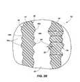
- the ammonium fluoride chemical treatment/plasma treatment processmay be used to reduce line width roughness (“LWR”) or line edge roughness (“LER”) of spacers formed from silicon oxide 14 , as illustrated in FIGS. 2A-2D .
- FIG. 2Aillustrates a semiconductor structure 10 including the substrate 12 having a hardmask composed of a pattern of oxide spacers 14 ′ thereon.
- the hardmaskis present in the form of free-standing lines or spacers (e.g., oxide spacers 14 ′) extending in a spaced, generally parallel relation to one another.
- the oxide spacers 14 ′may be formed from SiO, SiO 2 , ALD SiO, ALD SiO 2 , TEOS, or silicon-rich silicon oxynitride.
- the oxide spacers 14 ′may be formed as described in U.S. patent application Ser. No. 11/777,005, filed on Jul. 12, 2007, the entire disclosure of which is incorporated herein by reference.
- the oxide spacers 14 ′are formed to have a desired width or critical dimension (“CD”), such as, for example, from approximately 25 nm to approximately 50 nm, or from approximately 10 nm to approximately 20 nm. Since oxide spacers 14 ′ are formed on sidewalls of a patterned photoresist (not shown) or other material (not shown) by ALD, the conformal nature of the deposition process results in a transfer of the LWR that is present in the patterned photoresist to the oxide spacers 14 ′. As illustrated in FIG.
- CDcritical dimension
- the oxide spacers 14 ′exhibit a LWR or deviation of CD (width), denoted as CD 1-4 , along the length of the oxide spacer 14 ′ due to a profile of an edge 16 of the oxide spacers 14 ′ that is non-uniform and wavy with peaks 18 a (convex or elevated surface features) and valleys 18 b (concave or recessed surface features) along the vertical surfaces or sidewalls 20 and a variable peak-to-valley (or convex-to-concave) LWR amplitude 22 .
- the peaks 18 amay have a thickness or amplitude 22 of approximately 5 nm or less.
- the oxide spacers 14 ′may be subjected to the ammonium fluoride chemical treatment/plasma treatment process of an embodiment previously described.
- the ammonium fluoride chemical treatmentis described herein as using NH 3 , HF, and argon, and the plasma treatment is described as using argon and Cl 2 .
- each of these treatmentsmay include other gases, as previously described.
- the ammonium fluoride chemical treatment/plasma treatment processmay be conducted to achieve selective removal of small scale topography of the oxide spacers 14 ′ (versus trimming of the oxide spacers 14 ′ in bulk), for example, to reduce or eliminate the peaks 18 a of oxide spacers 14 ′, thus reshaping and straightening the profile of the edges 16 .
- the semiconductor structure 10may be placed in the vacuum chamber and NH 3 , HF, and argon introduced into the vacuum chamber.
- the ammonium fluoride chemical treatmentmay be used to convert the peaks 18 a to the solid reaction product 40 , as illustrated in FIG. 2C .
- the ammonium fluoride chemical treatmentmay be conducted under conditions that include a gas flow rate for each gas (NH 3 , HF) of from approximately 20 sccm to approximately 50 sccm; a gas flow rate for the inert carrier gas (argon) of from approximately 20 sccm to approximately 40 sccm; a NH 3 :HF flow rate (sccm) ratio of from approximately 2:1 to approximately 1:2; a partial pressure (pp) of HF of from approximately 5 mTorr to approximately 10 mTorr; an HF vapor temperature of from approximately 20° C.
- a gas flow rate for each gasNH 3 , HF
- argoninert carrier gas
- sccmNH 3 :HF flow rate
- pppartial pressure
- a gas pressure within the vacuum chamberof from approximately 10 mTorr to approximately 30 mTorr; a lid/wall chamber temperature of from approximately 60° C. to approximately 80° C.; a stage (substrate) temperature of from approximately 25° C. to approximately 45° C.; and an exposure time of from approximately 30 seconds to approximately 5 minutes.
- the solid reaction product 40may be removed by subjecting the oxide spacers 14 ′ to plasma treatment in an embodiment of the process. Since the ammonium fluoride chemical treatment included NH 3 and HF, the solid reaction product 40 is (NH 4 ) 2 SiF 6 . The argon and Cl 2 may be flowed into the vacuum chamber and an argon/Cl 2 plasma (not shown) generated. As the solid reaction product 40 is exposed to the argon/Cl 2 plasma, the (NH 4 ) 2 SiF 6 may be decomposed into N 2 , H 2 O, SiF 4 , NH 3 , or combinations thereof and evacuated from the vacuum chamber.
- the oxide spacers 14 ′may be subjected to additional cycles of the ammonium fluoride chemical treatment and the plasma treatment until a desired amount of the oxide spacers 14 ′ is removed.
- the peaks 18 a of the oxide spacers 14 ′may be removed, reducing the LWR/LER of the oxide spacers 14 ′.
- the oxide spacers 14 ′exhibit a deviation of CD, denoted as CD′ 1-4 , after removing the peaks 18 a.
- the semiconductor structure 10may be further processed as described in U.S. patent application Ser. No. 11/777,005. Because the ammonium fluoride chemical treatment/plasma treatment process is diffusion limited, there is generally faster (and greater) etching of more exposed convex areas (peaks 18 a ) than less exposed concave areas (valleys 18 b ) along the sidewalls 20 (edges 16 ) of the oxide spacers 14 ′ compared to a planar surface, resulting in a greater thickness of the solid reaction product 40 formed in the peaks 18 a over a fixed time period.
- Embodiments of the inventioncan thus be used to reduce or eliminate LWR and/or LER of the oxide spacers 14 ′ by laterally planarizing the sidewalls 20 of the oxide spacers 14 ′ to reduce the peak-to-valley LWR amplitude 22 to a desired edge profile for a more consistent CD measurement along the length of the oxide spacers 14 ′, and to achieve smoother edges 16 ′ and sidewall 20 ′ surfaces.
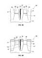
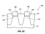
- the ammonium fluoride chemical treatment/plasma treatment processmay be used to remove silicon oxide 14 from a shallow trench isolation (“STI”) region 14 ′′, as illustrated in FIGS. 3A-3C .
- the STI region 14 ′′includes at least one cavity 114 therein. The presence of the cavity 114 affects substantially uniform removal of the silicon oxide.
- a memory array including the STI region 14 ′′may be formed by conventional techniques, which are not discussed in detail herein. FIG.
- the semiconductor structure 100may include a substrate 12 having a first dielectric material 104 thereon, a first conductive material 106 on the first dielectric material 104 , a hardmask 108 on the first conductive material 106 , the STI region 14 ′′, an active region 112 , and the at least one cavity 114 .
- the semiconductor structure 100is as described in U.S. patent application Ser. No. 11/652,218, filed on Jan. 11, 2007, the entire disclosure of which is incorporated herein by reference.
- the hardmask layer 108may be removed by conventional techniques, exposing an upper surface of the first conductive material 106 of each of the active regions 112 , as shown in FIG. 3B .
- a portion of the STI regions 14 ′′ of the semiconductor structure 100may be removed, even though the cavity 114 is present, so that the upper surface of the STI regions 14 ′′ lies below the upper surface of the first conductive material 106 .
- the STI regions 14 ′′may be anisotropically etched without substantially removing other exposed layers, such as first conductive material 106 .
- the portion of the STI regions 14 ′′may be removed by exposing the silicon oxide 14 of the STI regions 14 ′′ to the ammonium fluoride chemical treatment and forming the solid reaction product 40 .
- the chemical treatmentmay include NH 3 and HF, but is not limited thereto.
- the semiconductor structure 100may be subjected to the plasma treatment to remove the solid reaction product 40 .
- the plasma 4may be an argon/Cl 2 plasma, but is not limited thereto.
- the plasma 4may cause the solid reaction product 40 to decompose into N 2 , H 2 O, SiF 4 , CO 2 , NH 3 , or combinations thereof, which are exhausted from the vacuum chamber (not shown).
- FIG. 3Cillustrates the semiconductor structure 100 after removal of the solid reaction product 40 .
- the exposed portion of the STI regions 14 ′′may be exposed to multiple cycles of the ammonium fluoride chemical treatment and the plasma treatment to remove the desired amount of the silicon oxide 14 from the STI regions 14 ′′.
- additional materialmay be formed or disposed on the semiconductor structure 100 , as known in the art and as described and illustrated, for example, in U.S. patent application Ser. No. 11/652,218, the entire disclosure of which is incorporated herein by reference, to produce a memory device, such as a NAND FLASH memory device.
- FIG. 4Ashows semiconductor structure 3 in a reverse flow process for fabricating a memory device, such as a NAND FLASH memory device.
- the semiconductor structure 300may include an exposed sacrificial material 14 ′′′, at least one exposed STI region 14 ′′, and a semiconductor substrate 12 .
- the sacrificial material 14 ′′′may be formed from silicon oxide, such as a sacrificial oxide.
- the STI region 14 ′′may be formed from silicon oxide, such as an isolation oxide.
- the sacrificial material 14 ′′′may be in contact with the STI regions 14 ′′ and may function as a mask to protect the underlying semiconductor substrate 12 .
- the sacrificial material 14 ′′′may be substantially removed without substantially removing the STI region 14 ′′.
- the sacrificial material 14 ′′′may be removed without forming divots or “J-hooks” in the STI region 14 ′′.
- sidewalls 306 of the STI region 14 ′′may remain substantially vertical, with no etching occurring at interfaces of the sacrificial material 14 ′′′ with the STI region 14 ′′.
- the sacrificial material 14 ′′′may be subjected to the ammonium fluoride chemical treatment, as previously described, converting a portion of the sacrificial material 14 ′′′ to the solid reaction product 40 .
- FIG. 4Billustrates a semiconductor structure 300 having the solid reaction product 40 on the sacrificial material 14 ′′′.
- the solid reaction product 40prevents or inhibits etching of the sidewalls 306 of the STI region 14 ′′.
- the solid reaction product 40may be removed by subjecting the semiconductor structure 300 to the plasma treatment, as previously described.
- substantially all of the sacrificial material 14 ′′′may be removed by a single cycle of the ammonium fluoride chemical treatment and the plasma treatment. Alternatively, multiple cycles of the ammonium fluoride chemical treatment and the plasma treatment may be performed.
- a gate oxide layer 308may be formed over the substrate 12 by techniques known in the art to form semiconductor structure 300 , as illustrated in FIG. 4C .
- the semiconductor structure 300may be subjected to additional processing, as known in the art, to form an active area over the gate oxide layer 308 on the substrate 12 .
- the semiconductor structure 300may be exposed to the ammonium fluoride chemical treatment/plasma treatment process, as described above, to remove the sacrificial material 14 ′′′ without removing these other silicon oxide materials.
- these other silicon oxide materialsmay include, but are not limited to, TEOS, PSG, or BPSG.
- the semiconductor structures 2 , 10 , 100 , and 300 described abovemay be further processed by conventional techniques to produce memory devices including, but not limited to, a NAND FLASH device, a dynamic random access memory (“DRAM”) device, or other semiconductors devices.
- the memory or other semiconductor devicemay be used in wireless devices, personal computers, or other electronic devices, without limitation.
Landscapes
- Engineering & Computer Science (AREA)
- Chemical & Material Sciences (AREA)
- Manufacturing & Machinery (AREA)
- Physics & Mathematics (AREA)
- Condensed Matter Physics & Semiconductors (AREA)
- General Physics & Mathematics (AREA)
- Inorganic Chemistry (AREA)
- Computer Hardware Design (AREA)
- Microelectronics & Electronic Packaging (AREA)
- Power Engineering (AREA)
- Chemical Kinetics & Catalysis (AREA)
- General Chemical & Material Sciences (AREA)
- Drying Of Semiconductors (AREA)
Abstract
Description
- Embodiments of the invention relate to fabricating semiconductor structures and, more specifically, to removing silicon oxide from semiconductor structures.
- Chemical Oxide Removal (“COR”) is a gaseous process known in the art to selectively remove silicon oxides (“SiOx”) by reacting gaseous ammonia (“NH3”) and hydrogen fluoride (“HF”) to produce NH4Fx. The NH3and HF react with silicon oxide on a semiconductor wafer to form ammonium hexafluorosilicate (“(NH4)2SiF6”). This reaction is referred to herein as a “chemical treatment” and is typically conducted in a reaction chamber. The semiconductor wafer is then transferred to a different chamber and heated, producing nitrogen (“N2”), water (“H2O”), silicon tetrafluoride (“SiF4”), and NH3, which are volatile and evaporate from the surface of the semiconductor wafer. Heating the semiconductor wafer is referred to herein as a “post heat treatment (“PHT”).” Alternatively, the (NH4)2SiF6is removed using a deionized (“DI”) water rinse. The combination of the chemical treatment and the PHT is referred to herein as the “COR/PHT process.” The COR/PHT process is marketed under the tradename CERTAS® by Tokyo Electron Limited. Additional NH3/HF-based chemistries for etching oxides are marketed by ULVAC Technologies, Inc. (Methuen, Mass.) and Applied Materials, Inc. (Santa Clara, Calif.). Systems for conducting the COR/PHT process are known in the art. These systems include two chambers, one for conducting the chemical treatment and one for conducting the PHT. Semiconductor wafers undergoing the COR/PHT process are transported from one chamber to the other, which adds time to the wafer fabrication process and decreases wafer throughput.
- U.S. Pat. No. 6,951,821 discloses using the COR/PHT process to trim an oxide hard mask. The chemical treatment includes exposing the oxide hard mask to NH3and HF and the PHT includes heating the oxide hard mask to a temperature within a range of 20° C.-200° C. The COR/PHT process etches a thermal oxide at greater than 10 nm per 60 seconds of chemical treatment and tetraethyl orthosilicate (“TEOS”) at greater than 10 nm per 180 seconds of chemical treatment. The COR/PHT process has also been used to selectively remove small amounts (1 nm-30 nm) of silicon oxides, such as a native oxide or a thermal oxide, relative to polysilicon. United States Patent Application Publication No. 20060196527 discloses using the COR/PHT process to remove SiO2in a pre-metal-silicon contact formation cleaning, to remove SiO2before a silicon epitaxial process, or to remove SiO2from a polysilicon wafer before depositing a silicide metal.
- Furthermore, U.S. Pat. No. 7,091,069 discloses using a plasma or vapor of HF and NH3to remove a sacrificial oxide layer on a silicon-on-insulator (“SOI”) metal oxide semiconductor field effect transistor (“MOSFET”). U.S. Pat. No. 6,656,824 discloses using a plasma or vapor of HF and NH3to remove a sacrificial oxide layer in a MOSFET. The plasma or vapor of HF and NH3produces undercuts beneath silicon spacers formed on sidewalls of a dielectric layer of the MOSFET. U.S. Pat. No. 6,838,347 discloses etching concave portions of an oxide hardmask at a reduced rate relative to convex portions using a plasma or vapor of HF and NH3. Additionally, attempts have been made to reduce line defects on oxide-based mask lines by eliminating undesirable curves and protrusions, such as whiskers, using the COR/PHT process.
- United States Patent Application Publication No. 20060051966 discloses a method of removing oxides from a substrate and cleaning a processing chamber used to remove the oxides. The oxides are removed using a dry etchant that includes a mixture of NH3and nitrogen trifluoride (“NF3”). A plasma of the NH3/NF3mixture is generated and reacts with the oxides, forming (NH4)2SiF6. To remove the (NH4)2SiF6, the substrate is elevated in the processing chamber and annealed using a heated distribution plate, which provides thermal energy to dissociate the (NH4)2SiF6into volatile species. The processing chamber is periodically cleaned using high heat conductivity gases and heat or using a plasma.
- Accordingly, what is needed in the art are methods of removing silicon oxides from semiconductor wafers enabling improved wafer throughput.
FIGS. 1A-1C are cross-sectional views of a semiconductor structure during various stages of fabrication in accordance with an embodiment of the invention;FIG. 2A is a side view of a semiconductor structure during fabrication in accordance with an embodiment of the invention andFIGS. 2B-2D are cross-sectional views of the semiconductor structure depicted inFIG. 2A , taken alongline 2B-2B;FIGS. 3A-3C are cross-sectional views of a semiconductor structure in accordance with an embodiment of the invention, during various stages of fabrication; andFIGS. 4A-4C are cross-sectional views of a semiconductor structure in accordance with an embodiment of the invention, during various stages of fabrication.- A method of removing at least a portion of a silicon oxide material is disclosed. As shown in
FIGS. 1A-1C , asemiconductor structure 2 including asubstrate 12 and a silicon oxide14 (“SiOx”) is provided. A surface of thesilicon oxide 14 is exposed to an ammonium fluoride chemistry, forming asolid reaction product 40 on the surface of thesilicon oxide 14. As described in more detail below, the ammonium fluoride chemistry includes a volatile amine and HF. The reaction of the volatile amine and HF with thesilicon oxide 14 is referred to herein as “ammonium fluoride chemical treatment” to distinguish this reaction from the chemical treatment of the conventional COR/PHT process. Thesolid reaction product 40 andsilicon oxide 14 are exposed to aplasma 4, producing volatile species that are easily removed from a processing chamber (not shown) in which theplasma 4 is produced. Subjecting thesilicon oxide 14 and thesolid reaction product 40 to theplasma 4 is referred to herein as the “plasma treatment.” By converting a portion of thesilicon oxide 14 to thesolid reaction product 40 and volatilizing thesolid reaction product 40, that portion of thesilicon oxide 14 may be removed. The ion bombardment energy of theplasma 4 may be adjusted such that thesolid reaction product 40 is removed without removing theunreacted silicon oxide 14. To distinguish the process including the ammonium fluoride chemical treatment and the plasma treatment according to various embodiments of the invention from the conventional COR/PHT process, the former is referred to herein as the “ammonium fluoride chemical treatment/plasma treatment” process. - The following description provides specific details, such as material types and processing conditions in order to provide a thorough description of embodiments of the invention. However, a person of ordinary skill in the art will understand that these and other embodiments of the invention may be practiced without employing these specific details. Indeed, embodiments of the invention may be practiced in conjunction with conventional fabrication techniques employed in the industry. In addition, the semiconductor structures described below do not form a complete semiconductor device and the description provided below does not form a complete process flow for manufacturing the semiconductor device. Only those process acts and semiconductor structures necessary or desirable to understanding the embodiments of the invention are described in detail below. Additional acts to form the semiconductor device from the semiconductor structures may be performed by conventional fabrication techniques, which are, therefore, not described herein.
- As used herein, the term “silicon oxide” means and includes silicon dioxide (“SiO2”), silicon oxide (“SiO”), TEOS, a silicon-rich silicon oxynitride, atomic layer deposition (“ALD”) SiO or SiO2, or other silicon oxide-based material. The
silicon oxide 14 may be present on a surface of asubstrate 12 or in a trench or other opening formed in a surface of asubstrate 12.FIGS. 1A-1C ,3A-3C, and4A-4C illustrate thesilicon oxide 14 present in an opening in asubstrate 12 andFIGS. 2A-2D illustrate thesilicon oxide 14 present on the surface of asubstrate 12. If thesilicon oxide 14 is present in the opening in a substrate, the opening may have an aspect ratio (ratio of depth of the feature to width thereof) of less than or equal to approximately 20:1. - As used herein, the term “substrate” means and includes a conventional silicon substrate or other bulk substrate comprising a layer of semiconductive material. As used herein, the term “bulk substrate” means and includes not only silicon wafers, but also silicon-on-insulator (“SOI”) substrates, such as silicon-on-sapphire (“SOS”) substrates and silicon-on-glass (“SOG”) substrates, epitaxial layers of silicon on a base semiconductor foundation, and other semiconductor or optoelectronic materials, such as silicon-germanium, germanium, gallium arsenide, gallium nitride, or indium phosphide.
- To remove the
silicon oxide 14, thesemiconductor structure 2 including thesubstrate 12 and thesilicon oxide 14 may be exposed to the ammonium fluoride chemical treatment under appropriate conditions for the silicon oxide and the ammonium fluoride chemistry to react and form thesolid reaction product 40, as shown inFIG. 1B . The ammonium fluoride chemistry may include a gaseous mixture of at least one volatile amine and HF, which react with each other and with thesilicon oxide 14 to form thesolid reaction product 40. The volatile amine may be NH3or an alkylated derivative or alkylated analog of NH3, such as methyl amine, dimethyl amine, trimethyl amine, ethyl amine, diethyl amine, triethyl amine, isopropyl amine, dipropyl amine, n-propyl amine, n-butyl amine, sec-butyl amine, t-butyl amine, or combinations thereof. The gaseous mixture may, optionally, include an inert carrier gas, such as argon, xenon, neon, helium, or combinations thereof. The ammonium fluoride chemical treatment may be conducted in a processing chamber under appropriate process conditions for the reaction between the volatile amine, the HF, and thesilicon oxide 14 to occur. - The
semiconductor structure 2 may be placed in a processing apparatus and subjected to the ammonium fluoride chemical treatment, during which a portion of thesilicon oxide 14 on thesubstrate 12 is converted to thesolid reaction product 40. The processing apparatus may be configured to conduct both the ammonium fluoride chemical treatment and the plasma treatment in situ. The processing apparatus may be a conventional plasma chamber, such as an inductively coupled plasma chamber, modified to include gas supply lines for supplying the gases of the ammonium fluoride chemical treatment. The processing apparatus may include a vacuum chamber, a mounting table with a support (e.g., wafer chuck) for thesemiconductor structure 2 comprisingsubstrate 12, gas supply lines for the volatile amine and HF, gas supply lines for plasma-generating gases, a gas dispenser (e.g., a shower head) with a heating element to control the temperature of plasma-generating gas or gases, multiple openings leading from the gas dispenser for introducing the plasma-generating gas or gases into the vacuum chamber, at least one gas discharge port for removing gas from the vacuum chamber, a cooling channel for circulating a coolant into the mounting table to maintain thesemiconductor structure 2 comprisingsubstrate 12 at a desired temperature, a power source, and electrodes. The power source and electrodes may be used to convert the supplied gas or gases into a plasma including reactive species and to maintain the gas or gases as reactive species. Plasma chambers are known in the art and, therefore, are not described in additional detail herein. Processing apparatuses useful in practicing embodiments of the invention are commercially available from various sources, such as from Applied Materials, Inc. (Santa Clara, Calif.). - The volatile amine and HF for effecting an ammonium fluoride chemical treatment may be flowed into the processing apparatus through the gas supply lines and through the openings. Without being bound by any theory, it is believed that the volatile amine and HF react with one another and with the
silicon oxide 14 to form thesolid reaction product 40. By way of non-limiting example, if the ammonium fluoride chemistry includes a gaseous mixture of NH3and HF, (NH4)2SiF6is produced as thesolid reaction product 40. The NH3and HF are believed to react with one another to form NH4Fx, which reacts with thesilicon oxide 14 to form (NH4)2SiF6. Without being bound by any theory, it is believed that the mechanism for removing thesilicon oxide 14 is effected by diffusion of the ammonium fluoride chemistry into thesilicon oxide 14. As such, the removal of thesilicon oxide 14 is diffusion limited (self-limiting) and controllable. As a thickness of thesolid reaction product 40 on thesilicon oxide 14 increases, thesolid reaction product 40 functions as a barrier to gradually block and reduce diffusion of the NH4Fx, NH3, and/or HF into thesilicon oxide 14, which slows the rate of reaction and eventually terminates the ammonium fluoride chemical treatment. If (NH4)2SiF6is already present on thesilicon oxide 14, the NH3and HF may diffuse through the previously-formed (NH4)2SiF6to theunderlying silicon oxide 14 and react to form additional (NH4)2SiF6. By way of non-limiting example, if the ammonium fluoride chemistry includes a gaseous mixture of an alkylated NH3derivative (RxNH3-x, where x is an integer greater than or equal to 1) and HF, an alkylated derivative of (NH4)2SiF6, ((NRxH4-x)2SiF6, where x is an integer greater than or equal to 1), is produced as thesolid reaction product 40, where R is an alkyl group, such as methyl, ethyl, propyl, or butyl. For example, if the ammonium fluoride chemistry includes methyl amine and HF, the alkylated derivative (CH3—NH3)2SiF6may be formed as thesolid reaction product 40. - During the ammonium fluoride chemical treatment, the vacuum chamber may be maintained under appropriate conditions for the
silicon oxide 14 to be converted to thesolid reaction product 40. The amount ofsilicon oxide 14 that is converted during the ammonium fluoride chemical treatment may depend on at least one of the flow rate of the volatile amine and HF, the pressure in the vacuum chamber, the temperature within the vacuum chamber, and the exposure time. The gaseous mixture may include an equal volume of HF and the volatile amine, or a greater volume of the HF relative to the volatile amine. By way of non-limiting example, a volumetric flow rate ratio of the HF to the volatile amine in the gaseous mixture may be within a range of from approximately 1/1 to approximately 1/2. The flow range of NH3and HF may be in the range of approximately 20 sccm to approximately 50 sccm. If an inert carrier gas is present, the gaseous mixture of the HF and the volatile amine may account for from approximately 0.05% by volume to approximately 20% by volume of the total volume of the gaseous mixture and the inert carrier gas. - By way of non-limiting example, the pressure within the vacuum chamber during the ammonium fluoride chemical treatment may be maintained within a range of from approximately 6.7×10⁻²Pa to approximately 4.0 Pa (from approximately 0.5 mTorr to approximately 30 mTorr). By way of non-limiting example, the temperature within the vacuum chamber may be maintained within a range of from approximately 10° C. to approximately 30° C., such as at approximately room temperature (approximately 25° C.). The
silicon oxide 14 may be exposed to the ammonium fluoride chemical treatment for an amount of time sufficient to enable conversion of thesilicon oxide 14 to thesolid reaction product 40. By way of non-limiting example, the exposure time may be within a range of from approximately 30 seconds to approximately 300 seconds, such as from approximately 90 seconds to approximately 120 seconds. - To remove the
solid reaction product 40, thesubstrate 12 may be subjected to the plasma treatment in the vacuum chamber. Before conducting the plasma treatment, the vacuum chamber may be purged, such as with the inert gas, to remove excess reactants from the ammonium fluoride chemistry. The plasma treatment may cause thesolid reaction product 40 to decompose into volatile species, which are evacuated from the vacuum chamber. Theplasma 4 generated by the plasma treatment may be alow energy plasma 4 produced from at least one gas supplied through one or more of gas supply lines and termed for convenience a “plasma-generating gas.” Theplasma 4 may be produced by conventional techniques, such as by striking a plasma4 (seeFIG. 1B ) in the vacuum chamber. Theplasma 4 may include reactive species of the plasma-generating gases. By way of non-limiting example, the plasma-generating gas may be at least one inert gas, a mixture of the inert gas and a halogenated gas, hydrogen (“H2”), a mixture of the inert gas and hydrogen, or oxygen (“O2”). The inert gas may include, but is not limited to, argon, xenon, neon, helium, or combinations thereof. The halogenated gas may include at least one of chlorine (“Cl2”) and bromine (“Br2”). - In one embodiment, the plasma-generating gases include argon and Cl2. In another embodiment, the plasma-generating gas includes O2. If an alkylated NH3derivative is used as the volatile amine, producing an alkylated derivative of (NH4)2SiF6as the
solid reaction product 40, carbon residues from the alkylated derivative of (NH4)2SiF6may be produced on the surface of thesemiconductor structure 2. The PHT process (conventional heat treatment) described above may be ineffective at removing the carbon residues. However, since an O2plasma enables the formation of volatile carbon dioxide (“CO2”) from the carbon residues, the O2plasma may be used to remove the alkylated derivative of (NH4)2SiF6and the carbon residues. The O2plasma may also be used to remove (NH4)2SiF6. - In an additional embodiment, the plasma-generating gas includes H2. In addition to removing the
solid reaction product 40, using the H2plasma may provide improved surface passivation to a silicon substrate. In other words, using the H2plasma may achieve, in situ, removal of thesolid reaction product 40 and passivation of the silicon substrate. As such, a single vacuum chamber may be used to both remove thesolid reaction product 40 and provide the improved passivation of the silicon substrate. Using the H2plasma as the plasma treatment may increase the number of hydrogen-terminated surfaces on the silicon substrate, improving passivation, because hydrogen-terminated silicon surfaces are more resistant to oxidation than fluorine-terminated silicon surfaces. Hydrogen-terminated silicon surfaces are also more stable than fluorine-terminated silicon surfaces, which may form volatile SiFxcompounds, where x is from 1 to 4. Without being bound by any particular theory, it is believed that surface passivation is increased with use of the H2plasma via fluorine abstraction of the fluorine-terminated surfaces of the silicon substrate. Additionally, using the H2plasma may enable thesolid reaction product 40 to be removed at a low energy and without use of aggressive etch chemistries that may incorporate into the silicon substrate. In contrast, conventional HF vapor etch methods are known to produce fluorine-terminated surfaces on the silicon substrate. In addition, conventional, fluorine-based, dry etch methods for removing oxides are known to produce roughening of the silicon surface, diffusion of fluorine into the silicon substrate, residues on the surface of the silicon substrate, and liberation of O2from quartz components in the vacuum chamber. - The vacuum chamber may be maintained at appropriate conditions for the
low energy plasma 4 to be generated and maintained from the plasma-generating gases. These conditions may include, but are not limited to, the temperature and pressure within the vacuum chamber. By way of non-limiting example, the temperature within the vacuum chamber may be maintained within a range of from approximately −10° C. to approximately 80° C. The pressure within the vacuum chamber may be maintained within a range of from approximately 10 mTorr to approximately 500 mTorr, such as at approximately 200 mTorr. In addition, the flow rate of the plasma-generating gases may be adjusted. By way of non-limiting example, if the inert gas is used as the plasma-generating gas, the flow rate of the inert gas may be maintained within a range of from approximately 100 standard cubic centimeters per minute (“sccm”) to approximately 1000 sccm. If theplasma 4 is generated from the mixture of the inert gas and the halogenated gas, the flow rate of the halogenated gas may be maintained within a range of from approximately 10 sccm to approximately 200 sccm and the flow rate of the inert gas may be maintained within a range of from approximately 100 sccm to approximately 1000 sccm. If theplasma 4 is generated from the mixture of the inert gas and hydrogen, the flow rate of the inert gas may be maintained within a range of from approximately 100 sccm to approximately 1000 sccm and the flow rate of the hydrogen may be maintained within a range from approximately 10 sccm to approximately 200 sccm. - During the plasma treatment, the ion bombardment energy of the
plasma 4 may be maintained at less than or equal to approximately 20 eV, such as from approximately 1 eV to approximately 20 eV. Use of an ion bombardment energy within this range may help to reduce damage to the substrate and/or other exposed materials. Without being bound by any theory, it is believed that the energy used to decompose thesolid reaction product 40 may be provided by the ion bombardment energy of theplasma 4. The ion bombardment energy of theplasma 4 may be used to fluorinate thesolid reaction product 40. By way of non-limiting example, if thesolid reaction product 40 is (NH4)2SiF6, exposure to theplasma 4 may form (NFyH4-y)2SiF6, where y is from 1 to 4. As the value of y increases, volatile products of thesolid reaction product 40 may form and desorb or may be sputtered by ion impact. As such, removing thesolid reaction product 40 is not dependent on heat or a thermal act, but rather on a non-thermal act. In addition, without being bound by any theory, it is believed that the selectivity of the plasma treatment for thesolid reaction product 40 over thesilicon oxide 14 is provided by maintaining the ion bombardment energy within a range of from approximately 1 eV to approximately 20 eV. The activation energy for decomposing thesolid reaction product 40 is greater than or equal to approximately 1 eV. However, the activation energy for removingsilicon oxide 14 by physical sputtering is greater than approximately 20 eV. Therefore, by exposing thesolid reaction product 40 to theplasma 4 having an ion bombardment within this range, thesolid reaction product 40 may be removed without removing thesilicon oxide 14. While plasmas have been used in other aspects of semiconductor fabrication processing, these plasmas typically have a higher ion bombardment energy, such as greater than approximately 20 eV. As such, the use of theplasma 4 having an ion bombardment energy in the range of from approximately 1 eV to approximately 20 eV is unexpectedly low for a semiconductor fabrication process. - Exposing the
solid reaction product 40 to theplasma 4 may cause thesolid reaction product 40 to decompose and form volatile species, such as N2, H2O, SiF4, CO2, NH3, or combinations thereof. These volatile species may be evacuated from the vacuum chamber under vacuum or by using a purge gas. By exposing thesemiconductor structure 2 to theplasma 4, at least a portion of thesilicon oxide 14 converted to thesolid reaction product 40 may be anisotropically etched, as shown inFIG. 1C . By way of non-limiting example, thesilicon oxide 14 may be removed at a rate of from approximately 0.1 nm/second to approximately 20 nm/second. - After volatilization of the
solid reaction product 40, the vacuum chamber may be purged, such as with the inert carrier gas. Thesemiconductor structure 2 may then be subjected to an additional ammonium fluoride chemical treatment, as previously described, forming anothersolid reaction product 40 on thesilicon oxide 14. Thesolid reaction product 40 may be subjected to the plasma treatment, as previously described, to remove another portion of thesilicon oxide 14. By subjecting thesemiconductor structure 2 to multiple cycles of the ammonium fluoride chemical treatment and plasma treatment, a desired amount of thesilicon oxide 14 may be removed from thesubstrate 12. However, for the sake of convenience and clarity, only one cycle of the ammonium fluoride chemical treatment and plasma treatment is illustrated in each ofFIGS. 1A-1C and3A-4C. - Since the chemical treatment and the plasma treatment are conducted in a single processing apparatus, a wafer transport act is eliminated during fabrication of a semiconductor device formed from the
semiconductor structure 2. As such, wafer throughput may be increased. By way of non-limiting example, the wafer throughput enabled using processing according to embodiments of the invention may range from approximately 30 wafers/hour to approximately 50 wafers/hour. In contrast, the throughput of wafers subjected to the conventional COR/PHT process described previously is limited to approximately 20 wafers/hour. - To further increase the selectivity of the plasma treatment for the
solid reaction product 40 versus thesilicon oxide 14, the temperature within the vacuum chamber may be maintained at a lower level than is possible when using a conventional COR/PHT process. Since the activation energy for decomposing thesolid reaction product 40 is provided by the ion bombardment energy of theplasma 4, not thermal energy, the temperature of thesemiconductor structure 2 during the ammonium fluoride chemical treatment/plasma treatment process may be maintained at a lower temperature than during the conventional COR/PHT process. In the conventional COR/PHT process, the activation energy used to decompose thesolid reaction product 40 is produced from heat, or thermal energy. As such, thesolid reaction product 40 is thermally decomposed. While thesolid reaction product 40 is removed by the conventional COR/PHT process, another material having an activation energy greater than that of thesolid reaction product 40 may inadvertently be removed from a substrate subjected to this conventional processing. - Therefore, use of the ammonium fluoride chemical treatment/plasma treatment process may prevent or eliminate inadvertent removal of other materials exposed to the plasma treatment. Since the activation energy is supplied by the ion bombardment energy of the
plasma 4, the vacuum chamber may be maintained at a lower temperature compared to the temperature used during the conventional COR/PHT process. Additionally, the radical species generated by theplasma 4 do not depend on external activation energy from a heat source. Therefore, the decomposition of thesolid reaction product 40 may proceed without thermal stimulation. - As previously described, the ammonium fluoride chemical treatment/plasma treatment process may be used to selectively remove at least a portion of the
silicon oxide 14 from asemiconductor structure 2. Specific embodiments in which the ammonium fluoride chemical treatment/plasma treatment process may be used are described below. However, the ammonium fluoride chemical treatment/plasma treatment process is not limited to use in these embodiments. Rather, the ammonium fluoride chemical treatment/plasma treatment process may be used in any situation where selective removal of at least a portion of the silicon oxide is desired. - In one embodiment, the ammonium fluoride chemical treatment/plasma treatment process may be used to reduce line width roughness (“LWR”) or line edge roughness (“LER”) of spacers formed from
silicon oxide 14, as illustrated inFIGS. 2A-2D .FIG. 2A illustrates asemiconductor structure 10 including thesubstrate 12 having a hardmask composed of a pattern ofoxide spacers 14′ thereon. The hardmask is present in the form of free-standing lines or spacers (e.g.,oxide spacers 14′) extending in a spaced, generally parallel relation to one another. Theoxide spacers 14′ may be formed from SiO, SiO2, ALD SiO, ALD SiO2, TEOS, or silicon-rich silicon oxynitride. Theoxide spacers 14′ may be formed as described in U.S. patent application Ser. No. 11/777,005, filed on Jul. 12, 2007, the entire disclosure of which is incorporated herein by reference. - The
oxide spacers 14′ are formed to have a desired width or critical dimension (“CD”), such as, for example, from approximately 25 nm to approximately 50 nm, or from approximately 10 nm to approximately 20 nm. Sinceoxide spacers 14′ are formed on sidewalls of a patterned photoresist (not shown) or other material (not shown) by ALD, the conformal nature of the deposition process results in a transfer of the LWR that is present in the patterned photoresist to theoxide spacers 14′. As illustrated inFIG. 2B , theoxide spacers 14′ exhibit a LWR or deviation of CD (width), denoted as CD1-4, along the length of theoxide spacer 14′ due to a profile of anedge 16 of theoxide spacers 14′ that is non-uniform and wavy withpeaks 18a(convex or elevated surface features) andvalleys 18b(concave or recessed surface features) along the vertical surfaces orsidewalls 20 and a variable peak-to-valley (or convex-to-concave)LWR amplitude 22. By way of non-limiting example, thepeaks 18amay have a thickness oramplitude 22 of approximately 5 nm or less. - To decrease the LWR/LER, the
oxide spacers 14′ may be subjected to the ammonium fluoride chemical treatment/plasma treatment process of an embodiment previously described. By way of non-limiting example, the ammonium fluoride chemical treatment is described herein as using NH3, HF, and argon, and the plasma treatment is described as using argon and Cl2. However, each of these treatments may include other gases, as previously described. The ammonium fluoride chemical treatment/plasma treatment process may be conducted to achieve selective removal of small scale topography of theoxide spacers 14′ (versus trimming of theoxide spacers 14′ in bulk), for example, to reduce or eliminate thepeaks 18aofoxide spacers 14′, thus reshaping and straightening the profile of theedges 16. - The
semiconductor structure 10 may be placed in the vacuum chamber and NH3, HF, and argon introduced into the vacuum chamber. The ammonium fluoride chemical treatment may be used to convert thepeaks 18ato thesolid reaction product 40, as illustrated inFIG. 2C . The ammonium fluoride chemical treatment may be conducted under conditions that include a gas flow rate for each gas (NH3, HF) of from approximately 20 sccm to approximately 50 sccm; a gas flow rate for the inert carrier gas (argon) of from approximately 20 sccm to approximately 40 sccm; a NH3:HF flow rate (sccm) ratio of from approximately 2:1 to approximately 1:2; a partial pressure (pp) of HF of from approximately 5 mTorr to approximately 10 mTorr; an HF vapor temperature of from approximately 20° C. to approximately 70° C.; a gas pressure within the vacuum chamber of from approximately 10 mTorr to approximately 30 mTorr; a lid/wall chamber temperature of from approximately 60° C. to approximately 80° C.; a stage (substrate) temperature of from approximately 25° C. to approximately 45° C.; and an exposure time of from approximately 30 seconds to approximately 5 minutes. - As illustrated by the dashed line in
FIG. 2D , thesolid reaction product 40 may be removed by subjecting theoxide spacers 14′ to plasma treatment in an embodiment of the process. Since the ammonium fluoride chemical treatment included NH3and HF, thesolid reaction product 40 is (NH4)2SiF6. The argon and Cl2may be flowed into the vacuum chamber and an argon/Cl2plasma (not shown) generated. As thesolid reaction product 40 is exposed to the argon/Cl2plasma, the (NH4)2SiF6may be decomposed into N2, H2O, SiF4, NH3, or combinations thereof and evacuated from the vacuum chamber. Theoxide spacers 14′ may be subjected to additional cycles of the ammonium fluoride chemical treatment and the plasma treatment until a desired amount of theoxide spacers 14′ is removed. By converting thepeaks 18aof theoxide spacers 14′ to (NH4)2SiF6and decomposing the (NH4)2SiF6to form volatile species, thepeaks 18amay be removed, reducing the LWR/LER of theoxide spacers 14′. Theoxide spacers 14′ exhibit a deviation of CD, denoted as CD′1-4, after removing thepeaks 18a. - After removing the
peaks 18a,thesemiconductor structure 10 may be further processed as described in U.S. patent application Ser. No. 11/777,005. Because the ammonium fluoride chemical treatment/plasma treatment process is diffusion limited, there is generally faster (and greater) etching of more exposed convex areas (peaks18a) than less exposed concave areas (valleys 18b) along the sidewalls20 (edges16) of theoxide spacers 14′ compared to a planar surface, resulting in a greater thickness of thesolid reaction product 40 formed in thepeaks 18aover a fixed time period. The higher or accelerated etch rate of higher surface areas (peaks18a) thanvalleys 18bresults in effective removal of convex or protruding thepeaks 18a.Embodiments of the invention can thus be used to reduce or eliminate LWR and/or LER of theoxide spacers 14′ by laterally planarizing thesidewalls 20 of theoxide spacers 14′ to reduce the peak-to-valley LWR amplitude 22 to a desired edge profile for a more consistent CD measurement along the length of theoxide spacers 14′, and to achievesmoother edges 16′ andsidewall 20′ surfaces. - In another embodiment, the ammonium fluoride chemical treatment/plasma treatment process may be used to remove
silicon oxide 14 from a shallow trench isolation (“STI”)region 14″, as illustrated inFIGS. 3A-3C . TheSTI region 14″ includes at least onecavity 114 therein. The presence of thecavity 114 affects substantially uniform removal of the silicon oxide. A memory array including theSTI region 14″ may be formed by conventional techniques, which are not discussed in detail herein.FIG. 3A illustrates asemiconductor structure 100 after several processing acts have already been conducted Thesemiconductor structure 100 may include asubstrate 12 having a firstdielectric material 104 thereon, a firstconductive material 106 on the firstdielectric material 104, ahardmask 108 on the firstconductive material 106, theSTI region 14″, anactive region 112, and the at least onecavity 114. Thesemiconductor structure 100 is as described in U.S. patent application Ser. No. 11/652,218, filed on Jan. 11, 2007, the entire disclosure of which is incorporated herein by reference. - The
hardmask layer 108 may be removed by conventional techniques, exposing an upper surface of the firstconductive material 106 of each of theactive regions 112, as shown inFIG. 3B . A portion of theSTI regions 14″ of thesemiconductor structure 100 may be removed, even though thecavity 114 is present, so that the upper surface of theSTI regions 14″ lies below the upper surface of the firstconductive material 106. TheSTI regions 14″ may be anisotropically etched without substantially removing other exposed layers, such as firstconductive material 106. The portion of theSTI regions 14″ may be removed by exposing thesilicon oxide 14 of theSTI regions 14″ to the ammonium fluoride chemical treatment and forming thesolid reaction product 40. The chemical treatment may include NH3and HF, but is not limited thereto. After the reaction is complete, thesemiconductor structure 100 may be subjected to the plasma treatment to remove thesolid reaction product 40. Theplasma 4 may be an argon/Cl2plasma, but is not limited thereto. Theplasma 4 may cause thesolid reaction product 40 to decompose into N2, H2O, SiF4, CO2, NH3, or combinations thereof, which are exhausted from the vacuum chamber (not shown).FIG. 3C illustrates thesemiconductor structure 100 after removal of thesolid reaction product 40. The exposed portion of theSTI regions 14″ may be exposed to multiple cycles of the ammonium fluoride chemical treatment and the plasma treatment to remove the desired amount of thesilicon oxide 14 from theSTI regions 14″. - After the desired amount of the
STI regions 14″ is removed, additional material may be formed or disposed on thesemiconductor structure 100, as known in the art and as described and illustrated, for example, in U.S. patent application Ser. No. 11/652,218, the entire disclosure of which is incorporated herein by reference, to produce a memory device, such as a NAND FLASH memory device. - In another embodiment, the ammonium fluoride chemical treatment/plasma treatment process may be used to remove a sacrificial oxide without substantially removing an isolation oxide, as shown in
FIGS. 4A-4C .FIG. 4A showssemiconductor structure 3 in a reverse flow process for fabricating a memory device, such as a NAND FLASH memory device. Thesemiconductor structure 300 may include an exposedsacrificial material 14′″, at least oneexposed STI region 14″, and asemiconductor substrate 12. Thesacrificial material 14′″ may be formed from silicon oxide, such as a sacrificial oxide. TheSTI region 14″ may be formed from silicon oxide, such as an isolation oxide. Thesacrificial material 14′″ may be in contact with theSTI regions 14″ and may function as a mask to protect theunderlying semiconductor substrate 12. - The
sacrificial material 14′″ may be substantially removed without substantially removing theSTI region 14″. For instance, thesacrificial material 14′″ may be removed without forming divots or “J-hooks” in theSTI region 14″. In other words, sidewalls306 of theSTI region 14″ may remain substantially vertical, with no etching occurring at interfaces of thesacrificial material 14′″ with theSTI region 14″. Thesacrificial material 14′″ may be subjected to the ammonium fluoride chemical treatment, as previously described, converting a portion of thesacrificial material 14′″ to thesolid reaction product 40.FIG. 4B illustrates asemiconductor structure 300 having thesolid reaction product 40 on thesacrificial material 14′″. Without being bound by a particular theory, it is believed that thesolid reaction product 40 prevents or inhibits etching of thesidewalls 306 of theSTI region 14″. Thesolid reaction product 40 may be removed by subjecting thesemiconductor structure 300 to the plasma treatment, as previously described. Depending on the thickness of thesacrificial material 14′″, substantially all of thesacrificial material 14′″ may be removed by a single cycle of the ammonium fluoride chemical treatment and the plasma treatment. Alternatively, multiple cycles of the ammonium fluoride chemical treatment and the plasma treatment may be performed. Agate oxide layer 308 may be formed over thesubstrate 12 by techniques known in the art to formsemiconductor structure 300, as illustrated inFIG. 4C . Thesemiconductor structure 300 may be subjected to additional processing, as known in the art, to form an active area over thegate oxide layer 308 on thesubstrate 12. - If the
semiconductor structure 300 includes exposed layers (not shown) formed from other silicon oxide materials, thesemiconductor structure 300 may be exposed to the ammonium fluoride chemical treatment/plasma treatment process, as described above, to remove thesacrificial material 14′″ without removing these other silicon oxide materials. By way of non-limiting examples, these other silicon oxide materials may include, but are not limited to, TEOS, PSG, or BPSG. - The
semiconductor structures - While the invention is susceptible to various modifications as well as alternative forms and implementations, specific embodiments have been shown in the drawings and have been described in detail herein. However, the scope of the invention is not limited to the particular embodiments disclosed. Rather, the invention, in various embodiments, encompasses all modifications, equivalents, and alternatives falling within the scope of the invention as defined by the following appended claims and their legal equivalents.
Claims (25)
Priority Applications (2)
| Application Number | Priority Date | Filing Date | Title |
|---|---|---|---|
| US12/114,380US8252194B2 (en) | 2008-05-02 | 2008-05-02 | Methods of removing silicon oxide |
| US13/570,866US9005473B2 (en) | 2008-05-02 | 2012-08-09 | Gaseous compositions comprising hydrogen fluoride and an alkylated ammonia derivative |
Applications Claiming Priority (1)
| Application Number | Priority Date | Filing Date | Title |
|---|---|---|---|
| US12/114,380US8252194B2 (en) | 2008-05-02 | 2008-05-02 | Methods of removing silicon oxide |
Related Child Applications (1)
| Application Number | Title | Priority Date | Filing Date |
|---|---|---|---|
| US13/570,866DivisionUS9005473B2 (en) | 2008-05-02 | 2012-08-09 | Gaseous compositions comprising hydrogen fluoride and an alkylated ammonia derivative |
Publications (2)
| Publication Number | Publication Date |
|---|---|
| US20090275205A1true US20090275205A1 (en) | 2009-11-05 |
| US8252194B2 US8252194B2 (en) | 2012-08-28 |
Family
ID=41257388
Family Applications (2)
| Application Number | Title | Priority Date | Filing Date |
|---|---|---|---|
| US12/114,380Active2031-05-27US8252194B2 (en) | 2008-05-02 | 2008-05-02 | Methods of removing silicon oxide |
| US13/570,866Active2028-05-18US9005473B2 (en) | 2008-05-02 | 2012-08-09 | Gaseous compositions comprising hydrogen fluoride and an alkylated ammonia derivative |
Family Applications After (1)
| Application Number | Title | Priority Date | Filing Date |
|---|---|---|---|
| US13/570,866Active2028-05-18US9005473B2 (en) | 2008-05-02 | 2012-08-09 | Gaseous compositions comprising hydrogen fluoride and an alkylated ammonia derivative |
Country Status (1)
| Country | Link |
|---|---|
| US (2) | US8252194B2 (en) |
Cited By (563)
| Publication number | Priority date | Publication date | Assignee | Title |
|---|---|---|---|---|
| US20100255218A1 (en)* | 2009-04-01 | 2010-10-07 | Asm Japan K.K. | Method of Depositing Silicon Oxide Film by Plasma Enhanced Atomic Layer Deposition at Low Temperature |
| US20100255654A1 (en)* | 2009-04-07 | 2010-10-07 | Taiwan Semiconductor Manufacturing Company, Ltd. | Method for fabricating an isolation structure |
| US20100295148A1 (en)* | 2007-01-11 | 2010-11-25 | Micron Technology, Inc. | Methods of uniformly removing silicon oxide and an intermediate semiconductor device |
| US20120009796A1 (en)* | 2010-07-09 | 2012-01-12 | Applied Materials, Inc. | Post-ash sidewall healing |
| US20120055401A1 (en)* | 2007-12-27 | 2012-03-08 | Tokyo Electron Limited | Substrate processing method and system |
| US20130137240A1 (en)* | 2011-11-28 | 2013-05-30 | Samsung Electronics Co., Ltd. | Methods for fabricating semiconductor devices |
| US8679982B2 (en) | 2011-08-26 | 2014-03-25 | Applied Materials, Inc. | Selective suppression of dry-etch rate of materials containing both silicon and oxygen |
| US8679983B2 (en) | 2011-09-01 | 2014-03-25 | Applied Materials, Inc. | Selective suppression of dry-etch rate of materials containing both silicon and nitrogen |
| WO2014055235A1 (en)* | 2012-10-02 | 2014-04-10 | Applied Materials, Inc. | Directional sio2 etch using plasma pre-treatment and high-temperature etchant deposition |
| WO2014055236A1 (en)* | 2012-10-03 | 2014-04-10 | Applied Materials, Inc. | Directional sio2 etch using low-temperature etchant deposition and plasma post-treatment |
| US8741778B2 (en) | 2010-12-14 | 2014-06-03 | Applied Materials, Inc. | Uniform dry etch in two stages |
| US8765574B2 (en) | 2012-11-09 | 2014-07-01 | Applied Materials, Inc. | Dry etch process |
| US8771539B2 (en) | 2011-02-22 | 2014-07-08 | Applied Materials, Inc. | Remotely-excited fluorine and water vapor etch |
| US8771536B2 (en) | 2011-08-01 | 2014-07-08 | Applied Materials, Inc. | Dry-etch for silicon-and-carbon-containing films |
| US8801952B1 (en) | 2013-03-07 | 2014-08-12 | Applied Materials, Inc. | Conformal oxide dry etch |
| US8808563B2 (en) | 2011-10-07 | 2014-08-19 | Applied Materials, Inc. | Selective etch of silicon by way of metastable hydrogen termination |
| US8895449B1 (en) | 2013-05-16 | 2014-11-25 | Applied Materials, Inc. | Delicate dry clean |
| US8921234B2 (en) | 2012-12-21 | 2014-12-30 | Applied Materials, Inc. | Selective titanium nitride etching |
| US8927390B2 (en) | 2011-09-26 | 2015-01-06 | Applied Materials, Inc. | Intrench profile |
| US20150024600A1 (en)* | 2013-07-16 | 2015-01-22 | Taiwan Semiconductor Manufacturing Co., Ltd. | Systems and methods to mitigate nitride precipitates |
| US8951429B1 (en) | 2013-10-29 | 2015-02-10 | Applied Materials, Inc. | Tungsten oxide processing |
| US8956980B1 (en) | 2013-09-16 | 2015-02-17 | Applied Materials, Inc. | Selective etch of silicon nitride |
| US8969212B2 (en) | 2012-11-20 | 2015-03-03 | Applied Materials, Inc. | Dry-etch selectivity |
| US8975152B2 (en) | 2011-11-08 | 2015-03-10 | Applied Materials, Inc. | Methods of reducing substrate dislocation during gapfill processing |
| US8980761B2 (en) | 2012-10-03 | 2015-03-17 | Applied Materials, Inc. | Directional SIO2 etch using low-temperature etchant deposition and plasma post-treatment |
| US8980763B2 (en) | 2012-11-30 | 2015-03-17 | Applied Materials, Inc. | Dry-etch for selective tungsten removal |
| US8999856B2 (en) | 2011-03-14 | 2015-04-07 | Applied Materials, Inc. | Methods for etch of sin films |
| US20150111389A1 (en)* | 2013-10-21 | 2015-04-23 | Applied Materials, Inc. | Methods of surface interface engineering |
| US9023732B2 (en) | 2013-03-15 | 2015-05-05 | Applied Materials, Inc. | Processing systems and methods for halide scavenging |
| US9023734B2 (en) | 2012-09-18 | 2015-05-05 | Applied Materials, Inc. | Radical-component oxide etch |
| US9034770B2 (en) | 2012-09-17 | 2015-05-19 | Applied Materials, Inc. | Differential silicon oxide etch |
| US9040422B2 (en) | 2013-03-05 | 2015-05-26 | Applied Materials, Inc. | Selective titanium nitride removal |
| US9064815B2 (en) | 2011-03-14 | 2015-06-23 | Applied Materials, Inc. | Methods for etch of metal and metal-oxide films |
| US9064816B2 (en) | 2012-11-30 | 2015-06-23 | Applied Materials, Inc. | Dry-etch for selective oxidation removal |
| US9111877B2 (en) | 2012-12-18 | 2015-08-18 | Applied Materials, Inc. | Non-local plasma oxide etch |
| US9117855B2 (en) | 2013-12-04 | 2015-08-25 | Applied Materials, Inc. | Polarity control for remote plasma |
| US9114438B2 (en) | 2013-05-21 | 2015-08-25 | Applied Materials, Inc. | Copper residue chamber clean |
| US9132436B2 (en) | 2012-09-21 | 2015-09-15 | Applied Materials, Inc. | Chemical control features in wafer process equipment |
| US9136273B1 (en) | 2014-03-21 | 2015-09-15 | Applied Materials, Inc. | Flash gate air gap |
| US9159606B1 (en) | 2014-07-31 | 2015-10-13 | Applied Materials, Inc. | Metal air gap |
| US9165786B1 (en) | 2014-08-05 | 2015-10-20 | Applied Materials, Inc. | Integrated oxide and nitride recess for better channel contact in 3D architectures |
| US9177780B2 (en) | 2012-10-02 | 2015-11-03 | Applied Materials, Inc. | Directional SiO2 etch using plasma pre-treatment and high-temperature etchant deposition |
| US9190293B2 (en) | 2013-12-18 | 2015-11-17 | Applied Materials, Inc. | Even tungsten etch for high aspect ratio trenches |
| US9236265B2 (en) | 2013-11-04 | 2016-01-12 | Applied Materials, Inc. | Silicon germanium processing |
| US9245762B2 (en) | 2013-12-02 | 2016-01-26 | Applied Materials, Inc. | Procedure for etch rate consistency |
| US9263278B2 (en) | 2013-12-17 | 2016-02-16 | Applied Materials, Inc. | Dopant etch selectivity control |
| US9269590B2 (en) | 2014-04-07 | 2016-02-23 | Applied Materials, Inc. | Spacer formation |
| US9287095B2 (en) | 2013-12-17 | 2016-03-15 | Applied Materials, Inc. | Semiconductor system assemblies and methods of operation |
| US9287134B2 (en) | 2014-01-17 | 2016-03-15 | Applied Materials, Inc. | Titanium oxide etch |
| US9293568B2 (en) | 2014-01-27 | 2016-03-22 | Applied Materials, Inc. | Method of fin patterning |
| US9299575B2 (en) | 2014-03-17 | 2016-03-29 | Applied Materials, Inc. | Gas-phase tungsten etch |
| US9299538B2 (en) | 2014-03-20 | 2016-03-29 | Applied Materials, Inc. | Radial waveguide systems and methods for post-match control of microwaves |
| US9299583B1 (en) | 2014-12-05 | 2016-03-29 | Applied Materials, Inc. | Aluminum oxide selective etch |
| US9299537B2 (en) | 2014-03-20 | 2016-03-29 | Applied Materials, Inc. | Radial waveguide systems and methods for post-match control of microwaves |
| US9309598B2 (en) | 2014-05-28 | 2016-04-12 | Applied Materials, Inc. | Oxide and metal removal |
| US9324576B2 (en) | 2010-05-27 | 2016-04-26 | Applied Materials, Inc. | Selective etch for silicon films |
| US9324811B2 (en) | 2012-09-26 | 2016-04-26 | Asm Ip Holding B.V. | Structures and devices including a tensile-stressed silicon arsenic layer and methods of forming same |
| US9343272B1 (en) | 2015-01-08 | 2016-05-17 | Applied Materials, Inc. | Self-aligned process |
| US9349605B1 (en) | 2015-08-07 | 2016-05-24 | Applied Materials, Inc. | Oxide etch selectivity systems and methods |
| US9355862B2 (en) | 2014-09-24 | 2016-05-31 | Applied Materials, Inc. | Fluorine-based hardmask removal |
| US9355856B2 (en) | 2014-09-12 | 2016-05-31 | Applied Materials, Inc. | V trench dry etch |
| US9362130B2 (en) | 2013-03-01 | 2016-06-07 | Applied Materials, Inc. | Enhanced etching processes using remote plasma sources |
| US9368364B2 (en) | 2014-09-24 | 2016-06-14 | Applied Materials, Inc. | Silicon etch process with tunable selectivity to SiO2 and other materials |
| US9373517B2 (en) | 2012-08-02 | 2016-06-21 | Applied Materials, Inc. | Semiconductor processing with DC assisted RF power for improved control |
| US9373522B1 (en) | 2015-01-22 | 2016-06-21 | Applied Mateials, Inc. | Titanium nitride removal |
| US9378969B2 (en) | 2014-06-19 | 2016-06-28 | Applied Materials, Inc. | Low temperature gas-phase carbon removal |
| US9378978B2 (en) | 2014-07-31 | 2016-06-28 | Applied Materials, Inc. | Integrated oxide recess and floating gate fin trimming |
| US9384987B2 (en) | 2012-04-04 | 2016-07-05 | Asm Ip Holding B.V. | Metal oxide protective layer for a semiconductor device |
| US9385028B2 (en) | 2014-02-03 | 2016-07-05 | Applied Materials, Inc. | Air gap process |
| CN105742177A (en)* | 2016-03-11 | 2016-07-06 | 上海华力微电子有限公司 | Method for removing virtual gate electrode dielectric layer |
| US9390937B2 (en) | 2012-09-20 | 2016-07-12 | Applied Materials, Inc. | Silicon-carbon-nitride selective etch |
| US9396989B2 (en) | 2014-01-27 | 2016-07-19 | Applied Materials, Inc. | Air gaps between copper lines |
| US9394608B2 (en) | 2009-04-06 | 2016-07-19 | Asm America, Inc. | Semiconductor processing reactor and components thereof |
| US9404587B2 (en) | 2014-04-24 | 2016-08-02 | ASM IP Holding B.V | Lockout tagout for semiconductor vacuum valve |
| US9406523B2 (en) | 2014-06-19 | 2016-08-02 | Applied Materials, Inc. | Highly selective doped oxide removal method |
| US9412564B2 (en) | 2013-07-22 | 2016-08-09 | Asm Ip Holding B.V. | Semiconductor reaction chamber with plasma capabilities |
| US9425058B2 (en) | 2014-07-24 | 2016-08-23 | Applied Materials, Inc. | Simplified litho-etch-litho-etch process |
| US9449846B2 (en) | 2015-01-28 | 2016-09-20 | Applied Materials, Inc. | Vertical gate separation |
| US9447498B2 (en) | 2014-03-18 | 2016-09-20 | Asm Ip Holding B.V. | Method for performing uniform processing in gas system-sharing multiple reaction chambers |
| US9455138B1 (en) | 2015-11-10 | 2016-09-27 | Asm Ip Holding B.V. | Method for forming dielectric film in trenches by PEALD using H-containing gas |
| US9472417B2 (en) | 2013-11-12 | 2016-10-18 | Applied Materials, Inc. | Plasma-free metal etch |
| US9478415B2 (en) | 2015-02-13 | 2016-10-25 | Asm Ip Holding B.V. | Method for forming film having low resistance and shallow junction depth |
| US9478432B2 (en) | 2014-09-25 | 2016-10-25 | Applied Materials, Inc. | Silicon oxide selective removal |
| US9484191B2 (en) | 2013-03-08 | 2016-11-01 | Asm Ip Holding B.V. | Pulsed remote plasma method and system |
| US9496167B2 (en) | 2014-07-31 | 2016-11-15 | Applied Materials, Inc. | Integrated bit-line airgap formation and gate stack post clean |
| US9493879B2 (en) | 2013-07-12 | 2016-11-15 | Applied Materials, Inc. | Selective sputtering for pattern transfer |
| US9499898B2 (en) | 2014-03-03 | 2016-11-22 | Applied Materials, Inc. | Layered thin film heater and method of fabrication |
| US9502258B2 (en) | 2014-12-23 | 2016-11-22 | Applied Materials, Inc. | Anisotropic gap etch |
| CN106158640A (en)* | 2015-04-03 | 2016-11-23 | 中芯国际集成电路制造(上海)有限公司 | A kind of semiconductor device and preparation method thereof, electronic installation |
| US9543180B2 (en) | 2014-08-01 | 2017-01-10 | Asm Ip Holding B.V. | Apparatus and method for transporting wafers between wafer carrier and process tool under vacuum |
| US9553102B2 (en) | 2014-08-19 | 2017-01-24 | Applied Materials, Inc. | Tungsten separation |
| US9556516B2 (en) | 2013-10-09 | 2017-01-31 | ASM IP Holding B.V | Method for forming Ti-containing film by PEALD using TDMAT or TDEAT |
| US9558931B2 (en) | 2012-07-27 | 2017-01-31 | Asm Ip Holding B.V. | System and method for gas-phase sulfur passivation of a semiconductor surface |
| US9576809B2 (en) | 2013-11-04 | 2017-02-21 | Applied Materials, Inc. | Etch suppression with germanium |
| US9589770B2 (en) | 2013-03-08 | 2017-03-07 | Asm Ip Holding B.V. | Method and systems for in-situ formation of intermediate reactive species |
| US9605342B2 (en) | 2012-09-12 | 2017-03-28 | Asm Ip Holding B.V. | Process gas management for an inductively-coupled plasma deposition reactor |
| US9607837B1 (en) | 2015-12-21 | 2017-03-28 | Asm Ip Holding B.V. | Method for forming silicon oxide cap layer for solid state diffusion process |
| US9627221B1 (en) | 2015-12-28 | 2017-04-18 | Asm Ip Holding B.V. | Continuous process incorporating atomic layer etching |
| US9640416B2 (en) | 2012-12-26 | 2017-05-02 | Asm Ip Holding B.V. | Single-and dual-chamber module-attachable wafer-handling chamber |
| US9647114B2 (en) | 2015-08-14 | 2017-05-09 | Asm Ip Holding B.V. | Methods of forming highly p-type doped germanium tin films and structures and devices including the films |
| US9659753B2 (en) | 2014-08-07 | 2017-05-23 | Applied Materials, Inc. | Grooved insulator to reduce leakage current |
| US9659799B2 (en) | 2012-08-28 | 2017-05-23 | Asm Ip Holding B.V. | Systems and methods for dynamic semiconductor process scheduling |
| US9657845B2 (en) | 2014-10-07 | 2017-05-23 | Asm Ip Holding B.V. | Variable conductance gas distribution apparatus and method |
| US9691645B2 (en) | 2015-08-06 | 2017-06-27 | Applied Materials, Inc. | Bolted wafer chuck thermal management systems and methods for wafer processing systems |
| US9711345B2 (en) | 2015-08-25 | 2017-07-18 | Asm Ip Holding B.V. | Method for forming aluminum nitride-based film by PEALD |
| US9721789B1 (en) | 2016-10-04 | 2017-08-01 | Applied Materials, Inc. | Saving ion-damaged spacers |
| US9728437B2 (en) | 2015-02-03 | 2017-08-08 | Applied Materials, Inc. | High temperature chuck for plasma processing systems |
| US9735024B2 (en) | 2015-12-28 | 2017-08-15 | Asm Ip Holding B.V. | Method of atomic layer etching using functional group-containing fluorocarbon |
| US9741593B2 (en) | 2015-08-06 | 2017-08-22 | Applied Materials, Inc. | Thermal management systems and methods for wafer processing systems |
| US9754779B1 (en) | 2016-02-19 | 2017-09-05 | Asm Ip Holding B.V. | Method for forming silicon nitride film selectively on sidewalls or flat surfaces of trenches |
| US9768034B1 (en) | 2016-11-11 | 2017-09-19 | Applied Materials, Inc. | Removal methods for high aspect ratio structures |
| US9773648B2 (en) | 2013-08-30 | 2017-09-26 | Applied Materials, Inc. | Dual discharge modes operation for remote plasma |
| US9793148B2 (en) | 2011-06-22 | 2017-10-17 | Asm Japan K.K. | Method for positioning wafers in multiple wafer transport |
| US9793115B2 (en) | 2013-08-14 | 2017-10-17 | Asm Ip Holding B.V. | Structures and devices including germanium-tin films and methods of forming same |
| US9790595B2 (en) | 2013-07-12 | 2017-10-17 | Asm Ip Holding B.V. | Method and system to reduce outgassing in a reaction chamber |
| US9793135B1 (en) | 2016-07-14 | 2017-10-17 | ASM IP Holding B.V | Method of cyclic dry etching using etchant film |
| WO2017189482A1 (en)* | 2016-04-29 | 2017-11-02 | Applied Materials, Inc. | Methods for chemical etching of silicon |
| US9812320B1 (en) | 2016-07-28 | 2017-11-07 | Asm Ip Holding B.V. | Method and apparatus for filling a gap |
| US9847289B2 (en) | 2014-05-30 | 2017-12-19 | Applied Materials, Inc. | Protective via cap for improved interconnect performance |
| US9859151B1 (en) | 2016-07-08 | 2018-01-02 | Asm Ip Holding B.V. | Selective film deposition method to form air gaps |
| US9865484B1 (en) | 2016-06-29 | 2018-01-09 | Applied Materials, Inc. | Selective etch using material modification and RF pulsing |
| US9881805B2 (en) | 2015-03-02 | 2018-01-30 | Applied Materials, Inc. | Silicon selective removal |
| US9887082B1 (en) | 2016-07-28 | 2018-02-06 | Asm Ip Holding B.V. | Method and apparatus for filling a gap |
| US9885117B2 (en) | 2014-03-31 | 2018-02-06 | Applied Materials, Inc. | Conditioned semiconductor system parts |
| US9892908B2 (en) | 2011-10-28 | 2018-02-13 | Asm America, Inc. | Process feed management for semiconductor substrate processing |
| US9891521B2 (en) | 2014-11-19 | 2018-02-13 | Asm Ip Holding B.V. | Method for depositing thin film |
| US9890456B2 (en) | 2014-08-21 | 2018-02-13 | Asm Ip Holding B.V. | Method and system for in situ formation of gas-phase compounds |
| US9899291B2 (en) | 2015-07-13 | 2018-02-20 | Asm Ip Holding B.V. | Method for protecting layer by forming hydrocarbon-based extremely thin film |
| US9899405B2 (en) | 2014-12-22 | 2018-02-20 | Asm Ip Holding B.V. | Semiconductor device and manufacturing method thereof |
| US9905420B2 (en) | 2015-12-01 | 2018-02-27 | Asm Ip Holding B.V. | Methods of forming silicon germanium tin films and structures and devices including the films |
| US9909214B2 (en) | 2015-10-15 | 2018-03-06 | Asm Ip Holding B.V. | Method for depositing dielectric film in trenches by PEALD |
| US9916980B1 (en) | 2016-12-15 | 2018-03-13 | Asm Ip Holding B.V. | Method of forming a structure on a substrate |
| US9934942B1 (en) | 2016-10-04 | 2018-04-03 | Applied Materials, Inc. | Chamber with flow-through source |
| US9947549B1 (en) | 2016-10-10 | 2018-04-17 | Applied Materials, Inc. | Cobalt-containing material removal |
| US9960072B2 (en) | 2015-09-29 | 2018-05-01 | Asm Ip Holding B.V. | Variable adjustment for precise matching of multiple chamber cavity housings |
| US10026621B2 (en) | 2016-11-14 | 2018-07-17 | Applied Materials, Inc. | SiN spacer profile patterning |
| US10032628B2 (en) | 2016-05-02 | 2018-07-24 | Asm Ip Holding B.V. | Source/drain performance through conformal solid state doping |
| US10043684B1 (en) | 2017-02-06 | 2018-08-07 | Applied Materials, Inc. | Self-limiting atomic thermal etching systems and methods |
| US10043674B1 (en) | 2017-08-04 | 2018-08-07 | Applied Materials, Inc. | Germanium etching systems and methods |
| US10043661B2 (en) | 2015-07-13 | 2018-08-07 | Asm Ip Holding B.V. | Method for protecting layer by forming hydrocarbon-based extremely thin film |
| US10049891B1 (en) | 2017-05-31 | 2018-08-14 | Applied Materials, Inc. | Selective in situ cobalt residue removal |
| US10062587B2 (en) | 2012-07-18 | 2018-08-28 | Applied Materials, Inc. | Pedestal with multi-zone temperature control and multiple purge capabilities |
| US10062579B2 (en) | 2016-10-07 | 2018-08-28 | Applied Materials, Inc. | Selective SiN lateral recess |
| US10062575B2 (en) | 2016-09-09 | 2018-08-28 | Applied Materials, Inc. | Poly directional etch by oxidation |
| US10062585B2 (en) | 2016-10-04 | 2018-08-28 | Applied Materials, Inc. | Oxygen compatible plasma source |
| US10083836B2 (en) | 2015-07-24 | 2018-09-25 | Asm Ip Holding B.V. | Formation of boron-doped titanium metal films with high work function |
| US10087522B2 (en) | 2016-04-21 | 2018-10-02 | Asm Ip Holding B.V. | Deposition of metal borides |
| US10087525B2 (en) | 2015-08-04 | 2018-10-02 | Asm Ip Holding B.V. | Variable gap hard stop design |
| US10090316B2 (en) | 2016-09-01 | 2018-10-02 | Asm Ip Holding B.V. | 3D stacked multilayer semiconductor memory using doped select transistor channel |
| USD830981S1 (en) | 2017-04-07 | 2018-10-16 | Asm Ip Holding B.V. | Susceptor for semiconductor substrate processing apparatus |
| US10103040B1 (en) | 2017-03-31 | 2018-10-16 | Asm Ip Holding B.V. | Apparatus and method for manufacturing a semiconductor device |
| US10128086B1 (en) | 2017-10-24 | 2018-11-13 | Applied Materials, Inc. | Silicon pretreatment for nitride removal |
| US10134757B2 (en) | 2016-11-07 | 2018-11-20 | Asm Ip Holding B.V. | Method of processing a substrate and a device manufactured by using the method |
| US10163696B2 (en) | 2016-11-11 | 2018-12-25 | Applied Materials, Inc. | Selective cobalt removal for bottom up gapfill |
| US10170336B1 (en) | 2017-08-04 | 2019-01-01 | Applied Materials, Inc. | Methods for anisotropic control of selective silicon removal |
| US10167557B2 (en) | 2014-03-18 | 2019-01-01 | Asm Ip Holding B.V. | Gas distribution system, reactor including the system, and methods of using the same |
| US10170282B2 (en) | 2013-03-08 | 2019-01-01 | Applied Materials, Inc. | Insulated semiconductor faceplate designs |
| US10177025B2 (en) | 2016-07-28 | 2019-01-08 | Asm Ip Holding B.V. | Method and apparatus for filling a gap |
| US10179947B2 (en) | 2013-11-26 | 2019-01-15 | Asm Ip Holding B.V. | Method for forming conformal nitrided, oxidized, or carbonized dielectric film by atomic layer deposition |
| US10190213B2 (en) | 2016-04-21 | 2019-01-29 | Asm Ip Holding B.V. | Deposition of metal borides |
| US10211308B2 (en) | 2015-10-21 | 2019-02-19 | Asm Ip Holding B.V. | NbMC layers |
| US10224210B2 (en) | 2014-12-09 | 2019-03-05 | Applied Materials, Inc. | Plasma processing system with direct outlet toroidal plasma source |
| US10229833B2 (en) | 2016-11-01 | 2019-03-12 | Asm Ip Holding B.V. | Methods for forming a transition metal nitride film on a substrate by atomic layer deposition and related semiconductor device structures |
| US10236177B1 (en) | 2017-08-22 | 2019-03-19 | ASM IP Holding B.V.. | Methods for depositing a doped germanium tin semiconductor and related semiconductor device structures |
| US10242908B2 (en) | 2016-11-14 | 2019-03-26 | Applied Materials, Inc. | Airgap formation with damage-free copper |
| US10249524B2 (en) | 2017-08-09 | 2019-04-02 | Asm Ip Holding B.V. | Cassette holder assembly for a substrate cassette and holding member for use in such assembly |
| US10249577B2 (en) | 2016-05-17 | 2019-04-02 | Asm Ip Holding B.V. | Method of forming metal interconnection and method of fabricating semiconductor apparatus using the method |
| US10256079B2 (en) | 2013-02-08 | 2019-04-09 | Applied Materials, Inc. | Semiconductor processing systems having multiple plasma configurations |
| US10256112B1 (en) | 2017-12-08 | 2019-04-09 | Applied Materials, Inc. | Selective tungsten removal |
| US10262859B2 (en) | 2016-03-24 | 2019-04-16 | Asm Ip Holding B.V. | Process for forming a film on a substrate using multi-port injection assemblies |
| US10269558B2 (en) | 2016-12-22 | 2019-04-23 | Asm Ip Holding B.V. | Method of forming a structure on a substrate |
| US10276355B2 (en) | 2015-03-12 | 2019-04-30 | Asm Ip Holding B.V. | Multi-zone reactor, system including the reactor, and method of using the same |
| US10283321B2 (en) | 2011-01-18 | 2019-05-07 | Applied Materials, Inc. | Semiconductor processing system and methods using capacitively coupled plasma |
| US10283324B1 (en) | 2017-10-24 | 2019-05-07 | Applied Materials, Inc. | Oxygen treatment for nitride etching |
| US10283353B2 (en) | 2017-03-29 | 2019-05-07 | Asm Ip Holding B.V. | Method of reforming insulating film deposited on substrate with recess pattern |
| US10290508B1 (en) | 2017-12-05 | 2019-05-14 | Asm Ip Holding B.V. | Method for forming vertical spacers for spacer-defined patterning |
| US10297458B2 (en) | 2017-08-07 | 2019-05-21 | Applied Materials, Inc. | Process window widening using coated parts in plasma etch processes |
| US10312055B2 (en) | 2017-07-26 | 2019-06-04 | Asm Ip Holding B.V. | Method of depositing film by PEALD using negative bias |
| US10319588B2 (en) | 2017-10-10 | 2019-06-11 | Asm Ip Holding B.V. | Method for depositing a metal chalcogenide on a substrate by cyclical deposition |
| US10319600B1 (en) | 2018-03-12 | 2019-06-11 | Applied Materials, Inc. | Thermal silicon etch |
| US10319649B2 (en) | 2017-04-11 | 2019-06-11 | Applied Materials, Inc. | Optical emission spectroscopy (OES) for remote plasma monitoring |
| US10319739B2 (en) | 2017-02-08 | 2019-06-11 | Applied Materials, Inc. | Accommodating imperfectly aligned memory holes |
| US10322384B2 (en) | 2015-11-09 | 2019-06-18 | Asm Ip Holding B.V. | Counter flow mixer for process chamber |
| US10340135B2 (en) | 2016-11-28 | 2019-07-02 | Asm Ip Holding B.V. | Method of topologically restricted plasma-enhanced cyclic deposition of silicon or metal nitride |
| US10343920B2 (en) | 2016-03-18 | 2019-07-09 | Asm Ip Holding B.V. | Aligned carbon nanotubes |
| US10354889B2 (en) | 2017-07-17 | 2019-07-16 | Applied Materials, Inc. | Non-halogen etching of silicon-containing materials |
| US10361201B2 (en) | 2013-09-27 | 2019-07-23 | Asm Ip Holding B.V. | Semiconductor structure and device formed using selective epitaxial process |
| US10364496B2 (en) | 2011-06-27 | 2019-07-30 | Asm Ip Holding B.V. | Dual section module having shared and unshared mass flow controllers |
| US10367080B2 (en) | 2016-05-02 | 2019-07-30 | Asm Ip Holding B.V. | Method of forming a germanium oxynitride film |
| WO2019147583A1 (en)* | 2018-01-26 | 2019-08-01 | Lam Research Corporation | Spacer profile control using atomic layer deposition in a multiple patterning process |
| US10381219B1 (en) | 2018-10-25 | 2019-08-13 | Asm Ip Holding B.V. | Methods for forming a silicon nitride film |
| US10381226B2 (en) | 2016-07-27 | 2019-08-13 | Asm Ip Holding B.V. | Method of processing substrate |
| US10378106B2 (en) | 2008-11-14 | 2019-08-13 | Asm Ip Holding B.V. | Method of forming insulation film by modified PEALD |
| US10388513B1 (en) | 2018-07-03 | 2019-08-20 | Asm Ip Holding B.V. | Method for depositing silicon-free carbon-containing film as gap-fill layer by pulse plasma-assisted deposition |
| US10388509B2 (en) | 2016-06-28 | 2019-08-20 | Asm Ip Holding B.V. | Formation of epitaxial layers via dislocation filtering |
| US10395919B2 (en) | 2016-07-28 | 2019-08-27 | Asm Ip Holding B.V. | Method and apparatus for filling a gap |
| US10403507B2 (en) | 2017-02-03 | 2019-09-03 | Applied Materials, Inc. | Shaped etch profile with oxidation |
| US10403504B2 (en) | 2017-10-05 | 2019-09-03 | Asm Ip Holding B.V. | Method for selectively depositing a metallic film on a substrate |
| US10410943B2 (en) | 2016-10-13 | 2019-09-10 | Asm Ip Holding B.V. | Method for passivating a surface of a semiconductor and related systems |
| US10431429B2 (en) | 2017-02-03 | 2019-10-01 | Applied Materials, Inc. | Systems and methods for radial and azimuthal control of plasma uniformity |
| US10435790B2 (en) | 2016-11-01 | 2019-10-08 | Asm Ip Holding B.V. | Method of subatmospheric plasma-enhanced ALD using capacitively coupled electrodes with narrow gap |
| US10446393B2 (en) | 2017-05-08 | 2019-10-15 | Asm Ip Holding B.V. | Methods for forming silicon-containing epitaxial layers and related semiconductor device structures |
| US10458018B2 (en) | 2015-06-26 | 2019-10-29 | Asm Ip Holding B.V. | Structures including metal carbide material, devices including the structures, and methods of forming same |
| US10468251B2 (en) | 2016-02-19 | 2019-11-05 | Asm Ip Holding B.V. | Method for forming spacers using silicon nitride film for spacer-defined multiple patterning |
| US10468262B2 (en) | 2017-02-15 | 2019-11-05 | Asm Ip Holding B.V. | Methods for forming a metallic film on a substrate by a cyclical deposition and related semiconductor device structures |
| US10468267B2 (en) | 2017-05-31 | 2019-11-05 | Applied Materials, Inc. | Water-free etching methods |
| US10483099B1 (en) | 2018-07-26 | 2019-11-19 | Asm Ip Holding B.V. | Method for forming thermally stable organosilicon polymer film |
| US10490418B2 (en) | 2014-10-14 | 2019-11-26 | Applied Materials, Inc. | Systems and methods for internal surface conditioning assessment in plasma processing equipment |
| US10490406B2 (en) | 2018-04-10 | 2019-11-26 | Appled Materials, Inc. | Systems and methods for material breakthrough |
| US10497573B2 (en) | 2018-03-13 | 2019-12-03 | Applied Materials, Inc. | Selective atomic layer etching of semiconductor materials |
| US10504754B2 (en) | 2016-05-19 | 2019-12-10 | Applied Materials, Inc. | Systems and methods for improved semiconductor etching and component protection |
| US10501866B2 (en) | 2016-03-09 | 2019-12-10 | Asm Ip Holding B.V. | Gas distribution apparatus for improved film uniformity in an epitaxial system |
| US10504742B2 (en) | 2017-05-31 | 2019-12-10 | Asm Ip Holding B.V. | Method of atomic layer etching using hydrogen plasma |
| US10504700B2 (en) | 2015-08-27 | 2019-12-10 | Applied Materials, Inc. | Plasma etching systems and methods with secondary plasma injection |
| WO2019236509A1 (en)* | 2018-06-08 | 2019-12-12 | The Government Of The United States Of America, As Represented By The Secretary Of The Navy | Plasma-based process for production of f and hf from benign precursors and use of the same in room-temperature plasma processing |
| US10510536B2 (en) | 2018-03-29 | 2019-12-17 | Asm Ip Holding B.V. | Method of depositing a co-doped polysilicon film on a surface of a substrate within a reaction chamber |
| US10515815B2 (en) | 2017-11-21 | 2019-12-24 | Lam Research Corporation | Atomic layer deposition and etch in a single plasma chamber for fin field effect transistor formation |
| US10522371B2 (en) | 2016-05-19 | 2019-12-31 | Applied Materials, Inc. | Systems and methods for improved semiconductor etching and component protection |
| US10529542B2 (en) | 2015-03-11 | 2020-01-07 | Asm Ip Holdings B.V. | Cross-flow reactor and method |
| US10529554B2 (en) | 2016-02-19 | 2020-01-07 | Asm Ip Holding B.V. | Method for forming silicon nitride film selectively on sidewalls or flat surfaces of trenches |
| US10529563B2 (en) | 2017-03-29 | 2020-01-07 | Asm Ip Holdings B.V. | Method for forming doped metal oxide films on a substrate by cyclical deposition and related semiconductor device structures |
| US10535516B2 (en) | 2018-02-01 | 2020-01-14 | Asm Ip Holdings B.V. | Method for depositing a semiconductor structure on a surface of a substrate and related semiconductor structures |
| US10541184B2 (en) | 2017-07-11 | 2020-01-21 | Applied Materials, Inc. | Optical emission spectroscopic techniques for monitoring etching |
| US10541333B2 (en) | 2017-07-19 | 2020-01-21 | Asm Ip Holding B.V. | Method for depositing a group IV semiconductor and related semiconductor device structures |
| US10541246B2 (en) | 2017-06-26 | 2020-01-21 | Applied Materials, Inc. | 3D flash memory cells which discourage cross-cell electrical tunneling |
| US10546729B2 (en) | 2016-10-04 | 2020-01-28 | Applied Materials, Inc. | Dual-channel showerhead with improved profile |
| US10559458B1 (en) | 2018-11-26 | 2020-02-11 | Asm Ip Holding B.V. | Method of forming oxynitride film |
| US10566206B2 (en) | 2016-12-27 | 2020-02-18 | Applied Materials, Inc. | Systems and methods for anisotropic material breakthrough |
| US10573496B2 (en) | 2014-12-09 | 2020-02-25 | Applied Materials, Inc. | Direct outlet toroidal plasma source |
| US10573527B2 (en) | 2018-04-06 | 2020-02-25 | Applied Materials, Inc. | Gas-phase selective etching systems and methods |
| US10590535B2 (en) | 2017-07-26 | 2020-03-17 | Asm Ip Holdings B.V. | Chemical treatment, deposition and/or infiltration apparatus and method for using the same |
| US10593560B2 (en) | 2018-03-01 | 2020-03-17 | Applied Materials, Inc. | Magnetic induction plasma source for semiconductor processes and equipment |
| US10593523B2 (en) | 2014-10-14 | 2020-03-17 | Applied Materials, Inc. | Systems and methods for internal surface conditioning in plasma processing equipment |
| WO2020054476A1 (en)* | 2018-09-13 | 2020-03-19 | セントラル硝子株式会社 | Method and device for etching silicon oxide |
| US10600673B2 (en) | 2015-07-07 | 2020-03-24 | Asm Ip Holding B.V. | Magnetic susceptor to baseplate seal |
| US10607851B2 (en) | 2017-08-25 | 2020-03-31 | Micron Technology, Inc. | Vapor-etch cyclic process |
| US10605530B2 (en) | 2017-07-26 | 2020-03-31 | Asm Ip Holding B.V. | Assembly of a liner and a flange for a vertical furnace as well as the liner and the vertical furnace |
| US10607895B2 (en) | 2017-09-18 | 2020-03-31 | Asm Ip Holdings B.V. | Method for forming a semiconductor device structure comprising a gate fill metal |
| US10615047B2 (en) | 2018-02-28 | 2020-04-07 | Applied Materials, Inc. | Systems and methods to form airgaps |
| US10612137B2 (en) | 2016-07-08 | 2020-04-07 | Asm Ip Holdings B.V. | Organic reactants for atomic layer deposition |
| US10612136B2 (en) | 2018-06-29 | 2020-04-07 | ASM IP Holding, B.V. | Temperature-controlled flange and reactor system including same |
| USD880437S1 (en) | 2018-02-01 | 2020-04-07 | Asm Ip Holding B.V. | Gas supply plate for semiconductor manufacturing apparatus |
| US10629473B2 (en) | 2016-09-09 | 2020-04-21 | Applied Materials, Inc. | Footing removal for nitride spacer |
| US10643826B2 (en) | 2016-10-26 | 2020-05-05 | Asm Ip Holdings B.V. | Methods for thermally calibrating reaction chambers |
| US10643904B2 (en) | 2016-11-01 | 2020-05-05 | Asm Ip Holdings B.V. | Methods for forming a semiconductor device and related semiconductor device structures |
| US10655221B2 (en) | 2017-02-09 | 2020-05-19 | Asm Ip Holding B.V. | Method for depositing oxide film by thermal ALD and PEALD |
| US10658181B2 (en) | 2018-02-20 | 2020-05-19 | Asm Ip Holding B.V. | Method of spacer-defined direct patterning in semiconductor fabrication |
| US10658174B2 (en) | 2017-11-21 | 2020-05-19 | Lam Research Corporation | Atomic layer deposition and etch for reducing roughness |
| US10658205B2 (en) | 2017-09-28 | 2020-05-19 | Asm Ip Holdings B.V. | Chemical dispensing apparatus and methods for dispensing a chemical to a reaction chamber |
| US10672642B2 (en) | 2018-07-24 | 2020-06-02 | Applied Materials, Inc. | Systems and methods for pedestal configuration |
| US10679870B2 (en) | 2018-02-15 | 2020-06-09 | Applied Materials, Inc. | Semiconductor processing chamber multistage mixing apparatus |
| US10683571B2 (en) | 2014-02-25 | 2020-06-16 | Asm Ip Holding B.V. | Gas supply manifold and method of supplying gases to chamber using same |
| US10685834B2 (en) | 2017-07-05 | 2020-06-16 | Asm Ip Holdings B.V. | Methods for forming a silicon germanium tin layer and related semiconductor device structures |
| US10692741B2 (en) | 2017-08-08 | 2020-06-23 | Asm Ip Holdings B.V. | Radiation shield |
| US10699879B2 (en) | 2018-04-17 | 2020-06-30 | Applied Materials, Inc. | Two piece electrode assembly with gap for plasma control |
| US10707106B2 (en) | 2011-06-06 | 2020-07-07 | Asm Ip Holding B.V. | High-throughput semiconductor-processing apparatus equipped with multiple dual-chamber modules |
| US10714350B2 (en) | 2016-11-01 | 2020-07-14 | ASM IP Holdings, B.V. | Methods for forming a transition metal niobium nitride film on a substrate by atomic layer deposition and related semiconductor device structures |
| US10714335B2 (en) | 2017-04-25 | 2020-07-14 | Asm Ip Holding B.V. | Method of depositing thin film and method of manufacturing semiconductor device |
| US10714385B2 (en) | 2016-07-19 | 2020-07-14 | Asm Ip Holding B.V. | Selective deposition of tungsten |
| US10714315B2 (en) | 2012-10-12 | 2020-07-14 | Asm Ip Holdings B.V. | Semiconductor reaction chamber showerhead |
| US10727080B2 (en) | 2017-07-07 | 2020-07-28 | Applied Materials, Inc. | Tantalum-containing material removal |
| US10734238B2 (en) | 2017-11-21 | 2020-08-04 | Lam Research Corporation | Atomic layer deposition and etch in a single plasma chamber for critical dimension control |
| US10731249B2 (en) | 2018-02-15 | 2020-08-04 | Asm Ip Holding B.V. | Method of forming a transition metal containing film on a substrate by a cyclical deposition process, a method for supplying a transition metal halide compound to a reaction chamber, and related vapor deposition apparatus |
| US10734497B2 (en) | 2017-07-18 | 2020-08-04 | Asm Ip Holding B.V. | Methods for forming a semiconductor device structure and related semiconductor device structures |
| US10734244B2 (en) | 2017-11-16 | 2020-08-04 | Asm Ip Holding B.V. | Method of processing a substrate and a device manufactured by the same |
| US10755922B2 (en) | 2018-07-03 | 2020-08-25 | Asm Ip Holding B.V. | Method for depositing silicon-free carbon-containing film as gap-fill layer by pulse plasma-assisted deposition |
| US10755941B2 (en) | 2018-07-06 | 2020-08-25 | Applied Materials, Inc. | Self-limiting selective etching systems and methods |
| US10767789B2 (en) | 2018-07-16 | 2020-09-08 | Asm Ip Holding B.V. | Diaphragm valves, valve components, and methods for forming valve components |
| US10770286B2 (en) | 2017-05-08 | 2020-09-08 | Asm Ip Holdings B.V. | Methods for selectively forming a silicon nitride film on a substrate and related semiconductor device structures |
| US10770336B2 (en) | 2017-08-08 | 2020-09-08 | Asm Ip Holding B.V. | Substrate lift mechanism and reactor including same |
| US10797133B2 (en) | 2018-06-21 | 2020-10-06 | Asm Ip Holding B.V. | Method for depositing a phosphorus doped silicon arsenide film and related semiconductor device structures |
| US10804098B2 (en) | 2009-08-14 | 2020-10-13 | Asm Ip Holding B.V. | Systems and methods for thin-film deposition of metal oxides using excited nitrogen-oxygen species |
| US10811256B2 (en) | 2018-10-16 | 2020-10-20 | Asm Ip Holding B.V. | Method for etching a carbon-containing feature |
| US10818758B2 (en) | 2018-11-16 | 2020-10-27 | Asm Ip Holding B.V. | Methods for forming a metal silicate film on a substrate in a reaction chamber and related semiconductor device structures |
| USD900036S1 (en) | 2017-08-24 | 2020-10-27 | Asm Ip Holding B.V. | Heater electrical connector and adapter |
| US10829852B2 (en) | 2018-08-16 | 2020-11-10 | Asm Ip Holding B.V. | Gas distribution device for a wafer processing apparatus |
| US10847365B2 (en) | 2018-10-11 | 2020-11-24 | Asm Ip Holding B.V. | Method of forming conformal silicon carbide film by cyclic CVD |
| US10844484B2 (en) | 2017-09-22 | 2020-11-24 | Asm Ip Holding B.V. | Apparatus for dispensing a vapor phase reactant to a reaction chamber and related methods |
| US10847366B2 (en) | 2018-11-16 | 2020-11-24 | Asm Ip Holding B.V. | Methods for depositing a transition metal chalcogenide film on a substrate by a cyclical deposition process |
| US10847371B2 (en) | 2018-03-27 | 2020-11-24 | Asm Ip Holding B.V. | Method of forming an electrode on a substrate and a semiconductor device structure including an electrode |
| US10854426B2 (en) | 2018-01-08 | 2020-12-01 | Applied Materials, Inc. | Metal recess for semiconductor structures |
| US10854498B2 (en) | 2011-07-15 | 2020-12-01 | Asm Ip Holding B.V. | Wafer-supporting device and method for producing same |
| USD903477S1 (en) | 2018-01-24 | 2020-12-01 | Asm Ip Holdings B.V. | Metal clamp |
| US10858737B2 (en) | 2014-07-28 | 2020-12-08 | Asm Ip Holding B.V. | Showerhead assembly and components thereof |
| US10865475B2 (en) | 2016-04-21 | 2020-12-15 | Asm Ip Holding B.V. | Deposition of metal borides and silicides |
| US10867788B2 (en) | 2016-12-28 | 2020-12-15 | Asm Ip Holding B.V. | Method of forming a structure on a substrate |
| US10867786B2 (en) | 2018-03-30 | 2020-12-15 | Asm Ip Holding B.V. | Substrate processing method |
| US10872778B2 (en) | 2018-07-06 | 2020-12-22 | Applied Materials, Inc. | Systems and methods utilizing solid-phase etchants |
| US10872771B2 (en) | 2018-01-16 | 2020-12-22 | Asm Ip Holding B. V. | Method for depositing a material film on a substrate within a reaction chamber by a cyclical deposition process and related device structures |
| US10883175B2 (en) | 2018-08-09 | 2021-01-05 | Asm Ip Holding B.V. | Vertical furnace for processing substrates and a liner for use therein |
| US10886137B2 (en) | 2018-04-30 | 2021-01-05 | Applied Materials, Inc. | Selective nitride removal |
| US10886123B2 (en) | 2017-06-02 | 2021-01-05 | Asm Ip Holding B.V. | Methods for forming low temperature semiconductor layers and related semiconductor device structures |
| US10892198B2 (en) | 2018-09-14 | 2021-01-12 | Applied Materials, Inc. | Systems and methods for improved performance in semiconductor processing |
| US10892156B2 (en) | 2017-05-08 | 2021-01-12 | Asm Ip Holding B.V. | Methods for forming a silicon nitride film on a substrate and related semiconductor device structures |
| US10896820B2 (en) | 2018-02-14 | 2021-01-19 | Asm Ip Holding B.V. | Method for depositing a ruthenium-containing film on a substrate by a cyclical deposition process |
| US10903054B2 (en) | 2017-12-19 | 2021-01-26 | Applied Materials, Inc. | Multi-zone gas distribution systems and methods |
| US10910262B2 (en) | 2017-11-16 | 2021-02-02 | Asm Ip Holding B.V. | Method of selectively depositing a capping layer structure on a semiconductor device structure |
| US10914004B2 (en) | 2018-06-29 | 2021-02-09 | Asm Ip Holding B.V. | Thin-film deposition method and manufacturing method of semiconductor device |
| US10920320B2 (en) | 2017-06-16 | 2021-02-16 | Applied Materials, Inc. | Plasma health determination in semiconductor substrate processing reactors |
| US10923344B2 (en) | 2017-10-30 | 2021-02-16 | Asm Ip Holding B.V. | Methods for forming a semiconductor structure and related semiconductor structures |
| US10920319B2 (en) | 2019-01-11 | 2021-02-16 | Applied Materials, Inc. | Ceramic showerheads with conductive electrodes |
| US10928731B2 (en) | 2017-09-21 | 2021-02-23 | Asm Ip Holding B.V. | Method of sequential infiltration synthesis treatment of infiltrateable material and structures and devices formed using same |
| US10934619B2 (en) | 2016-11-15 | 2021-03-02 | Asm Ip Holding B.V. | Gas supply unit and substrate processing apparatus including the gas supply unit |
| US10941490B2 (en) | 2014-10-07 | 2021-03-09 | Asm Ip Holding B.V. | Multiple temperature range susceptor, assembly, reactor and system including the susceptor, and methods of using the same |
| US10943834B2 (en) | 2017-03-13 | 2021-03-09 | Applied Materials, Inc. | Replacement contact process |
| US10964512B2 (en) | 2018-02-15 | 2021-03-30 | Applied Materials, Inc. | Semiconductor processing chamber multistage mixing apparatus and methods |
| US10975470B2 (en) | 2018-02-23 | 2021-04-13 | Asm Ip Holding B.V. | Apparatus for detecting or monitoring for a chemical precursor in a high temperature environment |
| US11001925B2 (en) | 2016-12-19 | 2021-05-11 | Asm Ip Holding B.V. | Substrate processing apparatus |
| US11018047B2 (en) | 2018-01-25 | 2021-05-25 | Asm Ip Holding B.V. | Hybrid lift pin |
| US11015245B2 (en) | 2014-03-19 | 2021-05-25 | Asm Ip Holding B.V. | Gas-phase reactor and system having exhaust plenum and components thereof |
| US11018002B2 (en) | 2017-07-19 | 2021-05-25 | Asm Ip Holding B.V. | Method for selectively depositing a Group IV semiconductor and related semiconductor device structures |
| US11024523B2 (en) | 2018-09-11 | 2021-06-01 | Asm Ip Holding B.V. | Substrate processing apparatus and method |
| US11022879B2 (en) | 2017-11-24 | 2021-06-01 | Asm Ip Holding B.V. | Method of forming an enhanced unexposed photoresist layer |
| US11031242B2 (en) | 2018-11-07 | 2021-06-08 | Asm Ip Holding B.V. | Methods for depositing a boron doped silicon germanium film |
| USD922229S1 (en) | 2019-06-05 | 2021-06-15 | Asm Ip Holding B.V. | Device for controlling a temperature of a gas supply unit |
| US11049751B2 (en) | 2018-09-14 | 2021-06-29 | Asm Ip Holding B.V. | Cassette supply system to store and handle cassettes and processing apparatus equipped therewith |
| US11049755B2 (en) | 2018-09-14 | 2021-06-29 | Applied Materials, Inc. | Semiconductor substrate supports with embedded RF shield |
| US11056567B2 (en) | 2018-05-11 | 2021-07-06 | Asm Ip Holding B.V. | Method of forming a doped metal carbide film on a substrate and related semiconductor device structures |
| US11053591B2 (en) | 2018-08-06 | 2021-07-06 | Asm Ip Holding B.V. | Multi-port gas injection system and reactor system including same |
| US11056344B2 (en) | 2017-08-30 | 2021-07-06 | Asm Ip Holding B.V. | Layer forming method |
| US11062887B2 (en) | 2018-09-17 | 2021-07-13 | Applied Materials, Inc. | High temperature RF heater pedestals |
| US11069510B2 (en) | 2017-08-30 | 2021-07-20 | Asm Ip Holding B.V. | Substrate processing apparatus |
| US11081345B2 (en) | 2018-02-06 | 2021-08-03 | Asm Ip Holding B.V. | Method of post-deposition treatment for silicon oxide film |
| US11087997B2 (en) | 2018-10-31 | 2021-08-10 | Asm Ip Holding B.V. | Substrate processing apparatus for processing substrates |
| US11088002B2 (en) | 2018-03-29 | 2021-08-10 | Asm Ip Holding B.V. | Substrate rack and a substrate processing system and method |
| US11114283B2 (en) | 2018-03-16 | 2021-09-07 | Asm Ip Holding B.V. | Reactor, system including the reactor, and methods of manufacturing and using same |
| US11114294B2 (en) | 2019-03-08 | 2021-09-07 | Asm Ip Holding B.V. | Structure including SiOC layer and method of forming same |
| USD930782S1 (en) | 2019-08-22 | 2021-09-14 | Asm Ip Holding B.V. | Gas distributor |
| US11121002B2 (en) | 2018-10-24 | 2021-09-14 | Applied Materials, Inc. | Systems and methods for etching metals and metal derivatives |
| WO2021182311A1 (en)* | 2020-03-13 | 2021-09-16 | セントラル硝子株式会社 | Dry etching method, method for producing semiconductor device, and dry etching gas composition |
| US11127589B2 (en) | 2019-02-01 | 2021-09-21 | Asm Ip Holding B.V. | Method of topology-selective film formation of silicon oxide |
| US11127617B2 (en) | 2017-11-27 | 2021-09-21 | Asm Ip Holding B.V. | Storage device for storing wafer cassettes for use with a batch furnace |
| USD931978S1 (en) | 2019-06-27 | 2021-09-28 | Asm Ip Holding B.V. | Showerhead vacuum transport |
| US11139308B2 (en) | 2015-12-29 | 2021-10-05 | Asm Ip Holding B.V. | Atomic layer deposition of III-V compounds to form V-NAND devices |
| US11139191B2 (en) | 2017-08-09 | 2021-10-05 | Asm Ip Holding B.V. | Storage apparatus for storing cassettes for substrates and processing apparatus equipped therewith |
| US11158513B2 (en) | 2018-12-13 | 2021-10-26 | Asm Ip Holding B.V. | Methods for forming a rhenium-containing film on a substrate by a cyclical deposition process and related semiconductor device structures |
| USD935572S1 (en) | 2019-05-24 | 2021-11-09 | Asm Ip Holding B.V. | Gas channel plate |
| US11171025B2 (en) | 2019-01-22 | 2021-11-09 | Asm Ip Holding B.V. | Substrate processing device |
| US11205585B2 (en) | 2016-07-28 | 2021-12-21 | Asm Ip Holding B.V. | Substrate processing apparatus and method of operating the same |
| US11217444B2 (en) | 2018-11-30 | 2022-01-04 | Asm Ip Holding B.V. | Method for forming an ultraviolet radiation responsive metal oxide-containing film |
| USD940837S1 (en) | 2019-08-22 | 2022-01-11 | Asm Ip Holding B.V. | Electrode |
| US11222772B2 (en) | 2016-12-14 | 2022-01-11 | Asm Ip Holding B.V. | Substrate processing apparatus |
| US11227782B2 (en) | 2019-07-31 | 2022-01-18 | Asm Ip Holding B.V. | Vertical batch furnace assembly |
| US11227789B2 (en) | 2019-02-20 | 2022-01-18 | Asm Ip Holding B.V. | Method and apparatus for filling a recess formed within a substrate surface |
| US11230766B2 (en) | 2018-03-29 | 2022-01-25 | Asm Ip Holding B.V. | Substrate processing apparatus and method |
| US11232963B2 (en) | 2018-10-03 | 2022-01-25 | Asm Ip Holding B.V. | Substrate processing apparatus and method |
| US11239061B2 (en) | 2014-11-26 | 2022-02-01 | Applied Materials, Inc. | Methods and systems to enhance process uniformity |
| US11251068B2 (en) | 2018-10-19 | 2022-02-15 | Asm Ip Holding B.V. | Substrate processing apparatus and substrate processing method |
| US11251040B2 (en) | 2019-02-20 | 2022-02-15 | Asm Ip Holding B.V. | Cyclical deposition method including treatment step and apparatus for same |
| US11257693B2 (en) | 2015-01-09 | 2022-02-22 | Applied Materials, Inc. | Methods and systems to improve pedestal temperature control |
| USD944946S1 (en) | 2019-06-14 | 2022-03-01 | Asm Ip Holding B.V. | Shower plate |
| US11270899B2 (en) | 2018-06-04 | 2022-03-08 | Asm Ip Holding B.V. | Wafer handling chamber with moisture reduction |
| US11276559B2 (en) | 2017-05-17 | 2022-03-15 | Applied Materials, Inc. | Semiconductor processing chamber for multiple precursor flow |
| US11276590B2 (en) | 2017-05-17 | 2022-03-15 | Applied Materials, Inc. | Multi-zone semiconductor substrate supports |
| US11274369B2 (en) | 2018-09-11 | 2022-03-15 | Asm Ip Holding B.V. | Thin film deposition method |
| US11282698B2 (en) | 2019-07-19 | 2022-03-22 | Asm Ip Holding B.V. | Method of forming topology-controlled amorphous carbon polymer film |
| US11286558B2 (en) | 2019-08-23 | 2022-03-29 | Asm Ip Holding B.V. | Methods for depositing a molybdenum nitride film on a surface of a substrate by a cyclical deposition process and related semiconductor device structures including a molybdenum nitride film |
| US11286562B2 (en) | 2018-06-08 | 2022-03-29 | Asm Ip Holding B.V. | Gas-phase chemical reactor and method of using same |
| US11289326B2 (en) | 2019-05-07 | 2022-03-29 | Asm Ip Holding B.V. | Method for reforming amorphous carbon polymer film |
| US11295980B2 (en) | 2017-08-30 | 2022-04-05 | Asm Ip Holding B.V. | Methods for depositing a molybdenum metal film over a dielectric surface of a substrate by a cyclical deposition process and related semiconductor device structures |
| USD947913S1 (en) | 2019-05-17 | 2022-04-05 | Asm Ip Holding B.V. | Susceptor shaft |
| USD948463S1 (en) | 2018-10-24 | 2022-04-12 | Asm Ip Holding B.V. | Susceptor for semiconductor substrate supporting apparatus |
| US11306395B2 (en) | 2017-06-28 | 2022-04-19 | Asm Ip Holding B.V. | Methods for depositing a transition metal nitride film on a substrate by atomic layer deposition and related deposition apparatus |
| USD949319S1 (en) | 2019-08-22 | 2022-04-19 | Asm Ip Holding B.V. | Exhaust duct |
| US11315794B2 (en) | 2019-10-21 | 2022-04-26 | Asm Ip Holding B.V. | Apparatus and methods for selectively etching films |
| US11328909B2 (en) | 2017-12-22 | 2022-05-10 | Applied Materials, Inc. | Chamber conditioning and removal processes |
| US11342216B2 (en) | 2019-02-20 | 2022-05-24 | Asm Ip Holding B.V. | Cyclical deposition method and apparatus for filling a recess formed within a substrate surface |
| US11339476B2 (en) | 2019-10-08 | 2022-05-24 | Asm Ip Holding B.V. | Substrate processing device having connection plates, substrate processing method |
| US11345999B2 (en) | 2019-06-06 | 2022-05-31 | Asm Ip Holding B.V. | Method of using a gas-phase reactor system including analyzing exhausted gas |
| US11355338B2 (en) | 2019-05-10 | 2022-06-07 | Asm Ip Holding B.V. | Method of depositing material onto a surface and structure formed according to the method |
| US11361990B2 (en) | 2018-05-28 | 2022-06-14 | Asm Ip Holding B.V. | Substrate processing method and device manufactured by using the same |
| US11374112B2 (en) | 2017-07-19 | 2022-06-28 | Asm Ip Holding B.V. | Method for depositing a group IV semiconductor and related semiconductor device structures |
| US11378337B2 (en) | 2019-03-28 | 2022-07-05 | Asm Ip Holding B.V. | Door opener and substrate processing apparatus provided therewith |
| US11390946B2 (en) | 2019-01-17 | 2022-07-19 | Asm Ip Holding B.V. | Methods of forming a transition metal containing film on a substrate by a cyclical deposition process |
| US11393690B2 (en) | 2018-01-19 | 2022-07-19 | Asm Ip Holding B.V. | Deposition method |
| US11390950B2 (en) | 2017-01-10 | 2022-07-19 | Asm Ip Holding B.V. | Reactor system and method to reduce residue buildup during a film deposition process |
| US11390945B2 (en) | 2019-07-03 | 2022-07-19 | Asm Ip Holding B.V. | Temperature control assembly for substrate processing apparatus and method of using same |
| US11401605B2 (en) | 2019-11-26 | 2022-08-02 | Asm Ip Holding B.V. | Substrate processing apparatus |
| US11417534B2 (en) | 2018-09-21 | 2022-08-16 | Applied Materials, Inc. | Selective material removal |
| US11414760B2 (en) | 2018-10-08 | 2022-08-16 | Asm Ip Holding B.V. | Substrate support unit, thin film deposition apparatus including the same, and substrate processing apparatus including the same |
| US11424119B2 (en) | 2019-03-08 | 2022-08-23 | Asm Ip Holding B.V. | Method for selective deposition of silicon nitride layer and structure including selectively-deposited silicon nitride layer |
| US11430674B2 (en) | 2018-08-22 | 2022-08-30 | Asm Ip Holding B.V. | Sensor array, apparatus for dispensing a vapor phase reactant to a reaction chamber and related methods |
| US11430640B2 (en) | 2019-07-30 | 2022-08-30 | Asm Ip Holding B.V. | Substrate processing apparatus |
| US11437241B2 (en) | 2020-04-08 | 2022-09-06 | Asm Ip Holding B.V. | Apparatus and methods for selectively etching silicon oxide films |
| US11437242B2 (en) | 2018-11-27 | 2022-09-06 | Applied Materials, Inc. | Selective removal of silicon-containing materials |
| US11443926B2 (en) | 2019-07-30 | 2022-09-13 | Asm Ip Holding B.V. | Substrate processing apparatus |
| US11447864B2 (en) | 2019-04-19 | 2022-09-20 | Asm Ip Holding B.V. | Layer forming method and apparatus |
| US11447861B2 (en) | 2016-12-15 | 2022-09-20 | Asm Ip Holding B.V. | Sequential infiltration synthesis apparatus and a method of forming a patterned structure |
| USD965044S1 (en) | 2019-08-19 | 2022-09-27 | Asm Ip Holding B.V. | Susceptor shaft |
| US11453943B2 (en) | 2016-05-25 | 2022-09-27 | Asm Ip Holding B.V. | Method for forming carbon-containing silicon/metal oxide or nitride film by ALD using silicon precursor and hydrocarbon precursor |
| USD965524S1 (en) | 2019-08-19 | 2022-10-04 | Asm Ip Holding B.V. | Susceptor support |
| US11469098B2 (en) | 2018-05-08 | 2022-10-11 | Asm Ip Holding B.V. | Methods for depositing an oxide film on a substrate by a cyclical deposition process and related device structures |
| US11473195B2 (en) | 2018-03-01 | 2022-10-18 | Asm Ip Holding B.V. | Semiconductor processing apparatus and a method for processing a substrate |
| US11476109B2 (en) | 2019-06-11 | 2022-10-18 | Asm Ip Holding B.V. | Method of forming an electronic structure using reforming gas, system for performing the method, and structure formed using the method |
| US11482418B2 (en) | 2018-02-20 | 2022-10-25 | Asm Ip Holding B.V. | Substrate processing method and apparatus |
| US11482412B2 (en) | 2018-01-19 | 2022-10-25 | Asm Ip Holding B.V. | Method for depositing a gap-fill layer by plasma-assisted deposition |
| US11482533B2 (en) | 2019-02-20 | 2022-10-25 | Asm Ip Holding B.V. | Apparatus and methods for plug fill deposition in 3-D NAND applications |
| US11488819B2 (en) | 2018-12-04 | 2022-11-01 | Asm Ip Holding B.V. | Method of cleaning substrate processing apparatus |
| US11488854B2 (en) | 2020-03-11 | 2022-11-01 | Asm Ip Holding B.V. | Substrate handling device with adjustable joints |
| US11495459B2 (en) | 2019-09-04 | 2022-11-08 | Asm Ip Holding B.V. | Methods for selective deposition using a sacrificial capping layer |
| US11492703B2 (en) | 2018-06-27 | 2022-11-08 | Asm Ip Holding B.V. | Cyclic deposition methods for forming metal-containing material and films and structures including the metal-containing material |
| US11499222B2 (en) | 2018-06-27 | 2022-11-15 | Asm Ip Holding B.V. | Cyclic deposition methods for forming metal-containing material and films and structures including the metal-containing material |
| US11501968B2 (en) | 2019-11-15 | 2022-11-15 | Asm Ip Holding B.V. | Method for providing a semiconductor device with silicon filled gaps |
| US11499226B2 (en) | 2018-11-02 | 2022-11-15 | Asm Ip Holding B.V. | Substrate supporting unit and a substrate processing device including the same |
| US11515188B2 (en) | 2019-05-16 | 2022-11-29 | Asm Ip Holding B.V. | Wafer boat handling device, vertical batch furnace and method |
| US11515187B2 (en) | 2020-05-01 | 2022-11-29 | Asm Ip Holding B.V. | Fast FOUP swapping with a FOUP handler |
| US11521851B2 (en) | 2020-02-03 | 2022-12-06 | Asm Ip Holding B.V. | Method of forming structures including a vanadium or indium layer |
| US11527400B2 (en) | 2019-08-23 | 2022-12-13 | Asm Ip Holding B.V. | Method for depositing silicon oxide film having improved quality by peald using bis(diethylamino)silane |
| US11527403B2 (en) | 2019-12-19 | 2022-12-13 | Asm Ip Holding B.V. | Methods for filling a gap feature on a substrate surface and related semiconductor structures |
| US11530876B2 (en) | 2020-04-24 | 2022-12-20 | Asm Ip Holding B.V. | Vertical batch furnace assembly comprising a cooling gas supply |
| US11532757B2 (en) | 2016-10-27 | 2022-12-20 | Asm Ip Holding B.V. | Deposition of charge trapping layers |
| US11530483B2 (en) | 2018-06-21 | 2022-12-20 | Asm Ip Holding B.V. | Substrate processing system |
| US11551925B2 (en) | 2019-04-01 | 2023-01-10 | Asm Ip Holding B.V. | Method for manufacturing a semiconductor device |
| US11551912B2 (en) | 2020-01-20 | 2023-01-10 | Asm Ip Holding B.V. | Method of forming thin film and method of modifying surface of thin film |
| US11557474B2 (en) | 2019-07-29 | 2023-01-17 | Asm Ip Holding B.V. | Methods for selective deposition utilizing n-type dopants and/or alternative dopants to achieve high dopant incorporation |
| USD975665S1 (en) | 2019-05-17 | 2023-01-17 | Asm Ip Holding B.V. | Susceptor shaft |
| US11562901B2 (en) | 2019-09-25 | 2023-01-24 | Asm Ip Holding B.V. | Substrate processing method |
| US11572620B2 (en) | 2018-11-06 | 2023-02-07 | Asm Ip Holding B.V. | Methods for selectively depositing an amorphous silicon film on a substrate |
| US11581186B2 (en) | 2016-12-15 | 2023-02-14 | Asm Ip Holding B.V. | Sequential infiltration synthesis apparatus |
| US11587815B2 (en) | 2019-07-31 | 2023-02-21 | Asm Ip Holding B.V. | Vertical batch furnace assembly |
| US11587814B2 (en) | 2019-07-31 | 2023-02-21 | Asm Ip Holding B.V. | Vertical batch furnace assembly |
| US11594600B2 (en) | 2019-11-05 | 2023-02-28 | Asm Ip Holding B.V. | Structures with doped semiconductor layers and methods and systems for forming same |
| USD979506S1 (en) | 2019-08-22 | 2023-02-28 | Asm Ip Holding B.V. | Insulator |
| US11594428B2 (en) | 2015-02-03 | 2023-02-28 | Applied Materials, Inc. | Low temperature chuck for plasma processing systems |
| US11594450B2 (en) | 2019-08-22 | 2023-02-28 | Asm Ip Holding B.V. | Method for forming a structure with a hole |
| US11605528B2 (en) | 2019-07-09 | 2023-03-14 | Asm Ip Holding B.V. | Plasma device using coaxial waveguide, and substrate treatment method |
| USD980814S1 (en) | 2021-05-11 | 2023-03-14 | Asm Ip Holding B.V. | Gas distributor for substrate processing apparatus |
| USD980813S1 (en) | 2021-05-11 | 2023-03-14 | Asm Ip Holding B.V. | Gas flow control plate for substrate processing apparatus |
| US11610774B2 (en) | 2019-10-02 | 2023-03-21 | Asm Ip Holding B.V. | Methods for forming a topographically selective silicon oxide film by a cyclical plasma-enhanced deposition process |
| US11615970B2 (en) | 2019-07-17 | 2023-03-28 | Asm Ip Holding B.V. | Radical assist ignition plasma system and method |
| USD981973S1 (en) | 2021-05-11 | 2023-03-28 | Asm Ip Holding B.V. | Reactor wall for substrate processing apparatus |
| US11626316B2 (en) | 2019-11-20 | 2023-04-11 | Asm Ip Holding B.V. | Method of depositing carbon-containing material on a surface of a substrate, structure formed using the method, and system for forming the structure |
| US11626308B2 (en) | 2020-05-13 | 2023-04-11 | Asm Ip Holding B.V. | Laser alignment fixture for a reactor system |
| US11629407B2 (en) | 2019-02-22 | 2023-04-18 | Asm Ip Holding B.V. | Substrate processing apparatus and method for processing substrates |
| US11629406B2 (en) | 2018-03-09 | 2023-04-18 | Asm Ip Holding B.V. | Semiconductor processing apparatus comprising one or more pyrometers for measuring a temperature of a substrate during transfer of the substrate |
| US11637014B2 (en) | 2019-10-17 | 2023-04-25 | Asm Ip Holding B.V. | Methods for selective deposition of doped semiconductor material |
| US11637011B2 (en) | 2019-10-16 | 2023-04-25 | Asm Ip Holding B.V. | Method of topology-selective film formation of silicon oxide |
| US11639548B2 (en) | 2019-08-21 | 2023-05-02 | Asm Ip Holding B.V. | Film-forming material mixed-gas forming device and film forming device |
| US11639811B2 (en) | 2017-11-27 | 2023-05-02 | Asm Ip Holding B.V. | Apparatus including a clean mini environment |
| US11646205B2 (en) | 2019-10-29 | 2023-05-09 | Asm Ip Holding B.V. | Methods of selectively forming n-type doped material on a surface, systems for selectively forming n-type doped material, and structures formed using same |
| US11643724B2 (en) | 2019-07-18 | 2023-05-09 | Asm Ip Holding B.V. | Method of forming structures using a neutral beam |
| US11646184B2 (en) | 2019-11-29 | 2023-05-09 | Asm Ip Holding B.V. | Substrate processing apparatus |
| US11644758B2 (en) | 2020-07-17 | 2023-05-09 | Asm Ip Holding B.V. | Structures and methods for use in photolithography |
| US11646204B2 (en) | 2020-06-24 | 2023-05-09 | Asm Ip Holding B.V. | Method for forming a layer provided with silicon |
| US11658035B2 (en) | 2020-06-30 | 2023-05-23 | Asm Ip Holding B.V. | Substrate processing method |
| US11658029B2 (en) | 2018-12-14 | 2023-05-23 | Asm Ip Holding B.V. | Method of forming a device structure using selective deposition of gallium nitride and system for same |
| US11664245B2 (en) | 2019-07-16 | 2023-05-30 | Asm Ip Holding B.V. | Substrate processing device |
| US11664199B2 (en) | 2018-10-19 | 2023-05-30 | Asm Ip Holding B.V. | Substrate processing apparatus and substrate processing method |
| US11664267B2 (en) | 2019-07-10 | 2023-05-30 | Asm Ip Holding B.V. | Substrate support assembly and substrate processing device including the same |
| US11674220B2 (en) | 2020-07-20 | 2023-06-13 | Asm Ip Holding B.V. | Method for depositing molybdenum layers using an underlayer |
| US11680839B2 (en) | 2019-08-05 | 2023-06-20 | Asm Ip Holding B.V. | Liquid level sensor for a chemical source vessel |
| US11682560B2 (en) | 2018-10-11 | 2023-06-20 | Applied Materials, Inc. | Systems and methods for hafnium-containing film removal |
| USD990534S1 (en) | 2020-09-11 | 2023-06-27 | Asm Ip Holding B.V. | Weighted lift pin |
| US11688603B2 (en) | 2019-07-17 | 2023-06-27 | Asm Ip Holding B.V. | Methods of forming silicon germanium structures |
| US11685991B2 (en) | 2018-02-14 | 2023-06-27 | Asm Ip Holding B.V. | Method for depositing a ruthenium-containing film on a substrate by a cyclical deposition process |
| USD990441S1 (en) | 2021-09-07 | 2023-06-27 | Asm Ip Holding B.V. | Gas flow control plate |
| US11705333B2 (en) | 2020-05-21 | 2023-07-18 | Asm Ip Holding B.V. | Structures including multiple carbon layers and methods of forming and using same |
| US11718913B2 (en) | 2018-06-04 | 2023-08-08 | Asm Ip Holding B.V. | Gas distribution system and reactor system including same |
| US11721527B2 (en) | 2019-01-07 | 2023-08-08 | Applied Materials, Inc. | Processing chamber mixing systems |
| US11725280B2 (en) | 2020-08-26 | 2023-08-15 | Asm Ip Holding B.V. | Method for forming metal silicon oxide and metal silicon oxynitride layers |
| US11725277B2 (en) | 2011-07-20 | 2023-08-15 | Asm Ip Holding B.V. | Pressure transmitter for a semiconductor processing environment |
| US11735422B2 (en) | 2019-10-10 | 2023-08-22 | Asm Ip Holding B.V. | Method of forming a photoresist underlayer and structure including same |
| US11742198B2 (en) | 2019-03-08 | 2023-08-29 | Asm Ip Holding B.V. | Structure including SiOCN layer and method of forming same |
| US11769682B2 (en) | 2017-08-09 | 2023-09-26 | Asm Ip Holding B.V. | Storage apparatus for storing cassettes for substrates and processing apparatus equipped therewith |
| US11767589B2 (en) | 2020-05-29 | 2023-09-26 | Asm Ip Holding B.V. | Substrate processing device |
| US11776846B2 (en) | 2020-02-07 | 2023-10-03 | Asm Ip Holding B.V. | Methods for depositing gap filling fluids and related systems and devices |
| US11781243B2 (en) | 2020-02-17 | 2023-10-10 | Asm Ip Holding B.V. | Method for depositing low temperature phosphorous-doped silicon |
| US11781221B2 (en) | 2019-05-07 | 2023-10-10 | Asm Ip Holding B.V. | Chemical source vessel with dip tube |
| US11804364B2 (en) | 2020-05-19 | 2023-10-31 | Asm Ip Holding B.V. | Substrate processing apparatus |
| US11814747B2 (en) | 2019-04-24 | 2023-11-14 | Asm Ip Holding B.V. | Gas-phase reactor system-with a reaction chamber, a solid precursor source vessel, a gas distribution system, and a flange assembly |
| US11821078B2 (en) | 2020-04-15 | 2023-11-21 | Asm Ip Holding B.V. | Method for forming precoat film and method for forming silicon-containing film |
| US11823866B2 (en) | 2020-04-02 | 2023-11-21 | Asm Ip Holding B.V. | Thin film forming method |
| US11823876B2 (en) | 2019-09-05 | 2023-11-21 | Asm Ip Holding B.V. | Substrate processing apparatus |
| US11830738B2 (en) | 2020-04-03 | 2023-11-28 | Asm Ip Holding B.V. | Method for forming barrier layer and method for manufacturing semiconductor device |
| US11830730B2 (en) | 2017-08-29 | 2023-11-28 | Asm Ip Holding B.V. | Layer forming method and apparatus |
| US11828707B2 (en) | 2020-02-04 | 2023-11-28 | Asm Ip Holding B.V. | Method and apparatus for transmittance measurements of large articles |
| US11827981B2 (en) | 2020-10-14 | 2023-11-28 | Asm Ip Holding B.V. | Method of depositing material on stepped structure |
| US11840761B2 (en) | 2019-12-04 | 2023-12-12 | Asm Ip Holding B.V. | Substrate processing apparatus |
| US11876356B2 (en) | 2020-03-11 | 2024-01-16 | Asm Ip Holding B.V. | Lockout tagout assembly and system and method of using same |
| US11873557B2 (en) | 2020-10-22 | 2024-01-16 | Asm Ip Holding B.V. | Method of depositing vanadium metal |
| US11885023B2 (en) | 2018-10-01 | 2024-01-30 | Asm Ip Holding B.V. | Substrate retaining apparatus, system including the apparatus, and method of using same |
| USD1012873S1 (en) | 2020-09-24 | 2024-01-30 | Asm Ip Holding B.V. | Electrode for semiconductor processing apparatus |
| US11885013B2 (en) | 2019-12-17 | 2024-01-30 | Asm Ip Holding B.V. | Method of forming vanadium nitride layer and structure including the vanadium nitride layer |
| US11887857B2 (en) | 2020-04-24 | 2024-01-30 | Asm Ip Holding B.V. | Methods and systems for depositing a layer comprising vanadium, nitrogen, and a further element |
| US11885020B2 (en) | 2020-12-22 | 2024-01-30 | Asm Ip Holding B.V. | Transition metal deposition method |
| US20240038526A1 (en)* | 2018-10-03 | 2024-02-01 | Lam Research Ag | Gas mixture including hydrogen fluoride, alcohol and an additive for preventing stiction of and/or repairing high aspect ratio structures |
| US11891696B2 (en) | 2020-11-30 | 2024-02-06 | Asm Ip Holding B.V. | Injector configured for arrangement within a reaction chamber of a substrate processing apparatus |
| US11898243B2 (en) | 2020-04-24 | 2024-02-13 | Asm Ip Holding B.V. | Method of forming vanadium nitride-containing layer |
| US11901179B2 (en) | 2020-10-28 | 2024-02-13 | Asm Ip Holding B.V. | Method and device for depositing silicon onto substrates |
| US11915929B2 (en) | 2019-11-26 | 2024-02-27 | Asm Ip Holding B.V. | Methods for selectively forming a target film on a substrate comprising a first dielectric surface and a second metallic surface |
| US11923181B2 (en) | 2019-11-29 | 2024-03-05 | Asm Ip Holding B.V. | Substrate processing apparatus for minimizing the effect of a filling gas during substrate processing |
| US11929251B2 (en) | 2019-12-02 | 2024-03-12 | Asm Ip Holding B.V. | Substrate processing apparatus having electrostatic chuck and substrate processing method |
| WO2024058794A1 (en)* | 2022-09-14 | 2024-03-21 | Applied Materials, Inc. | Methods of highly selective silicon oxide removal |
| US11946137B2 (en) | 2020-12-16 | 2024-04-02 | Asm Ip Holding B.V. | Runout and wobble measurement fixtures |
| US11959168B2 (en) | 2020-04-29 | 2024-04-16 | Asm Ip Holding B.V. | Solid source precursor vessel |
| US11961741B2 (en) | 2020-03-12 | 2024-04-16 | Asm Ip Holding B.V. | Method for fabricating layer structure having target topological profile |
| USD1023959S1 (en) | 2021-05-11 | 2024-04-23 | Asm Ip Holding B.V. | Electrode for substrate processing apparatus |
| US11967488B2 (en) | 2013-02-01 | 2024-04-23 | Asm Ip Holding B.V. | Method for treatment of deposition reactor |
| US11976359B2 (en) | 2020-01-06 | 2024-05-07 | Asm Ip Holding B.V. | Gas supply assembly, components thereof, and reactor system including same |
| US11986868B2 (en) | 2020-02-28 | 2024-05-21 | Asm Ip Holding B.V. | System dedicated for parts cleaning |
| US11987881B2 (en) | 2020-05-22 | 2024-05-21 | Asm Ip Holding B.V. | Apparatus for depositing thin films using hydrogen peroxide |
| US11996309B2 (en) | 2019-05-16 | 2024-05-28 | Asm Ip Holding B.V. | Wafer boat handling device, vertical batch furnace and method |
| US11996292B2 (en) | 2019-10-25 | 2024-05-28 | Asm Ip Holding B.V. | Methods for filling a gap feature on a substrate surface and related semiconductor structures |
| US11993843B2 (en) | 2017-08-31 | 2024-05-28 | Asm Ip Holding B.V. | Substrate processing apparatus |
| US11993847B2 (en) | 2020-01-08 | 2024-05-28 | Asm Ip Holding B.V. | Injector |
| US11996289B2 (en) | 2020-04-16 | 2024-05-28 | Asm Ip Holding B.V. | Methods of forming structures including silicon germanium and silicon layers, devices formed using the methods, and systems for performing the methods |
| US12006572B2 (en) | 2019-10-08 | 2024-06-11 | Asm Ip Holding B.V. | Reactor system including a gas distribution assembly for use with activated species and method of using same |
| US12009224B2 (en) | 2020-09-29 | 2024-06-11 | Asm Ip Holding B.V. | Apparatus and method for etching metal nitrides |
| US12009241B2 (en) | 2019-10-14 | 2024-06-11 | Asm Ip Holding B.V. | Vertical batch furnace assembly with detector to detect cassette |
| US12020934B2 (en) | 2020-07-08 | 2024-06-25 | Asm Ip Holding B.V. | Substrate processing method |
| US12025484B2 (en) | 2018-05-08 | 2024-07-02 | Asm Ip Holding B.V. | Thin film forming method |
| US12027365B2 (en) | 2020-11-24 | 2024-07-02 | Asm Ip Holding B.V. | Methods for filling a gap and related systems and devices |
| US12033885B2 (en) | 2020-01-06 | 2024-07-09 | Asm Ip Holding B.V. | Channeled lift pin |
| US12040177B2 (en) | 2020-08-18 | 2024-07-16 | Asm Ip Holding B.V. | Methods for forming a laminate film by cyclical plasma-enhanced deposition processes |
| US12040200B2 (en) | 2017-06-20 | 2024-07-16 | Asm Ip Holding B.V. | Semiconductor processing apparatus and methods for calibrating a semiconductor processing apparatus |
| US12040199B2 (en) | 2018-11-28 | 2024-07-16 | Asm Ip Holding B.V. | Substrate processing apparatus for processing substrates |
| US12051602B2 (en) | 2020-05-04 | 2024-07-30 | Asm Ip Holding B.V. | Substrate processing system for processing substrates with an electronics module located behind a door in a front wall of the substrate processing system |
| US12051567B2 (en) | 2020-10-07 | 2024-07-30 | Asm Ip Holding B.V. | Gas supply unit and substrate processing apparatus including gas supply unit |
| US12057314B2 (en) | 2020-05-15 | 2024-08-06 | Asm Ip Holding B.V. | Methods for silicon germanium uniformity control using multiple precursors |
| US12074022B2 (en) | 2020-08-27 | 2024-08-27 | Asm Ip Holding B.V. | Method and system for forming patterned structures using multiple patterning process |
| US12087586B2 (en) | 2020-04-15 | 2024-09-10 | Asm Ip Holding B.V. | Method of forming chromium nitride layer and structure including the chromium nitride layer |
| US12106944B2 (en) | 2020-06-02 | 2024-10-01 | Asm Ip Holding B.V. | Rotating substrate support |
| US12107005B2 (en) | 2020-10-06 | 2024-10-01 | Asm Ip Holding B.V. | Deposition method and an apparatus for depositing a silicon-containing material |
| US12112940B2 (en) | 2019-07-19 | 2024-10-08 | Asm Ip Holding B.V. | Method of forming topology-controlled amorphous carbon polymer film |
| US12125700B2 (en) | 2020-01-16 | 2024-10-22 | Asm Ip Holding B.V. | Method of forming high aspect ratio features |
| US12131885B2 (en) | 2020-12-22 | 2024-10-29 | Asm Ip Holding B.V. | Plasma treatment device having matching box |
| US12129545B2 (en) | 2020-12-22 | 2024-10-29 | Asm Ip Holding B.V. | Precursor capsule, a vessel and a method |
| US12148609B2 (en) | 2020-09-16 | 2024-11-19 | Asm Ip Holding B.V. | Silicon oxide deposition method |
| US12154824B2 (en) | 2020-08-14 | 2024-11-26 | Asm Ip Holding B.V. | Substrate processing method |
| US12159788B2 (en) | 2020-12-14 | 2024-12-03 | Asm Ip Holding B.V. | Method of forming structures for threshold voltage control |
| US12169361B2 (en) | 2019-07-30 | 2024-12-17 | Asm Ip Holding B.V. | Substrate processing apparatus and method |
| US12173404B2 (en) | 2020-03-17 | 2024-12-24 | Asm Ip Holding B.V. | Method of depositing epitaxial material, structure formed using the method, and system for performing the method |
| US12195852B2 (en) | 2020-11-23 | 2025-01-14 | Asm Ip Holding B.V. | Substrate processing apparatus with an injector |
| US12209308B2 (en) | 2020-11-12 | 2025-01-28 | Asm Ip Holding B.V. | Reactor and related methods |
| US12211742B2 (en) | 2020-09-10 | 2025-01-28 | Asm Ip Holding B.V. | Methods for depositing gap filling fluid |
| US12218000B2 (en) | 2020-09-25 | 2025-02-04 | Asm Ip Holding B.V. | Semiconductor processing method |
| USD1060598S1 (en) | 2021-12-03 | 2025-02-04 | Asm Ip Holding B.V. | Split showerhead cover |
| US12217946B2 (en) | 2020-10-15 | 2025-02-04 | Asm Ip Holding B.V. | Method of manufacturing semiconductor device, and substrate treatment apparatus using ether-CAT |
| US12218269B2 (en) | 2020-02-13 | 2025-02-04 | Asm Ip Holding B.V. | Substrate processing apparatus including light receiving device and calibration method of light receiving device |
| US12217954B2 (en) | 2020-08-25 | 2025-02-04 | Asm Ip Holding B.V. | Method of cleaning a surface |
| US12221357B2 (en) | 2020-04-24 | 2025-02-11 | Asm Ip Holding B.V. | Methods and apparatus for stabilizing vanadium compounds |
| US12230531B2 (en) | 2018-04-09 | 2025-02-18 | Asm Ip Holding B.V. | Substrate supporting apparatus, substrate processing apparatus including the same, and substrate processing method |
| US12243757B2 (en) | 2020-05-21 | 2025-03-04 | Asm Ip Holding B.V. | Flange and apparatus for processing substrates |
| US12243747B2 (en) | 2020-04-24 | 2025-03-04 | Asm Ip Holding B.V. | Methods of forming structures including vanadium boride and vanadium phosphide layers |
| US12243742B2 (en) | 2020-04-21 | 2025-03-04 | Asm Ip Holding B.V. | Method for processing a substrate |
| US12241158B2 (en) | 2020-07-20 | 2025-03-04 | Asm Ip Holding B.V. | Method for forming structures including transition metal layers |
| US12247286B2 (en) | 2019-08-09 | 2025-03-11 | Asm Ip Holding B.V. | Heater assembly including cooling apparatus and method of using same |
| US12255053B2 (en) | 2020-12-10 | 2025-03-18 | Asm Ip Holding B.V. | Methods and systems for depositing a layer |
| US12252785B2 (en) | 2019-06-10 | 2025-03-18 | Asm Ip Holding B.V. | Method for cleaning quartz epitaxial chambers |
| US12266524B2 (en) | 2020-06-16 | 2025-04-01 | Asm Ip Holding B.V. | Method for depositing boron containing silicon germanium layers |
| US12272527B2 (en) | 2018-05-09 | 2025-04-08 | Asm Ip Holding B.V. | Apparatus for use with hydrogen radicals and method of using same |
| US12278129B2 (en) | 2020-03-04 | 2025-04-15 | Asm Ip Holding B.V. | Alignment fixture for a reactor system |
| US12276023B2 (en) | 2017-08-04 | 2025-04-15 | Asm Ip Holding B.V. | Showerhead assembly for distributing a gas within a reaction chamber |
| US12288710B2 (en) | 2020-12-18 | 2025-04-29 | Asm Ip Holding B.V. | Wafer processing apparatus with a rotatable table |
| US12322591B2 (en) | 2020-07-27 | 2025-06-03 | Asm Ip Holding B.V. | Thin film deposition process |
| US12340979B2 (en) | 2017-05-17 | 2025-06-24 | Applied Materials, Inc. | Semiconductor processing chamber for improved precursor flow |
| US12378665B2 (en) | 2018-10-26 | 2025-08-05 | Asm Ip Holding B.V. | High temperature coatings for a preclean and etch apparatus and related methods |
| US12406846B2 (en) | 2020-05-26 | 2025-09-02 | Asm Ip Holding B.V. | Method for depositing boron and gallium containing silicon germanium layers |
| US12410515B2 (en) | 2020-01-29 | 2025-09-09 | Asm Ip Holding B.V. | Contaminant trap system for a reactor system |
| US12428726B2 (en) | 2019-10-08 | 2025-09-30 | Asm Ip Holding B.V. | Gas injection system and reactor system including same |
| US12431334B2 (en) | 2020-02-13 | 2025-09-30 | Asm Ip Holding B.V. | Gas distribution assembly |
| US12431354B2 (en) | 2020-07-01 | 2025-09-30 | Asm Ip Holding B.V. | Silicon nitride and silicon oxide deposition methods using fluorine inhibitor |
| US12444599B2 (en) | 2021-12-08 | 2025-10-14 | Asm Ip Holding B.V. | Method for forming an ultraviolet radiation responsive metal oxide-containing film |
Families Citing this family (27)
| Publication number | Priority date | Publication date | Assignee | Title |
|---|---|---|---|---|
| JP5661523B2 (en)* | 2011-03-18 | 2015-01-28 | 東京エレクトロン株式会社 | Film forming method and film forming apparatus |
| JP5997555B2 (en)* | 2012-09-14 | 2016-09-28 | 東京エレクトロン株式会社 | Etching apparatus and etching method |
| US9105587B2 (en) | 2012-11-08 | 2015-08-11 | Micron Technology, Inc. | Methods of forming semiconductor structures with sulfur dioxide etch chemistries |
| US9472453B2 (en) | 2014-03-13 | 2016-10-18 | Qualcomm Incorporated | Systems and methods of forming a reduced capacitance device |
| US9461144B2 (en)* | 2014-06-13 | 2016-10-04 | Taiwan Semiconductor Manufacturing Company, Ltd. | Method for semiconductor device fabrication |
| KR20160018921A (en)* | 2014-08-07 | 2016-02-18 | 삼성전자주식회사 | Semiconductor Memory Device And Method of Fabricating The Same |
| US9240315B1 (en) | 2014-10-10 | 2016-01-19 | Applied Materials, Inc. | CVD oxide surface pre-conditioning by inductively coupled O2 plasma |
| US9576811B2 (en) | 2015-01-12 | 2017-02-21 | Lam Research Corporation | Integrating atomic scale processes: ALD (atomic layer deposition) and ALE (atomic layer etch) |
| US9806252B2 (en) | 2015-04-20 | 2017-10-31 | Lam Research Corporation | Dry plasma etch method to pattern MRAM stack |
| US9870899B2 (en) | 2015-04-24 | 2018-01-16 | Lam Research Corporation | Cobalt etch back |
| US9595452B2 (en)* | 2015-05-27 | 2017-03-14 | Lam Research Corporation | Residue free oxide etch |
| US9972504B2 (en)* | 2015-08-07 | 2018-05-15 | Lam Research Corporation | Atomic layer etching of tungsten for enhanced tungsten deposition fill |
| US10096487B2 (en) | 2015-08-19 | 2018-10-09 | Lam Research Corporation | Atomic layer etching of tungsten and other metals |
| US9984858B2 (en) | 2015-09-04 | 2018-05-29 | Lam Research Corporation | ALE smoothness: in and outside semiconductor industry |
| US9917017B2 (en) | 2015-12-29 | 2018-03-13 | Taiwan Semiconductor Manufacturing Company, Ltd. | Replacement gate process for semiconductor devices |
| US10903083B2 (en)* | 2016-01-13 | 2021-01-26 | Tokyo Electron Limited | Substrate processing method, substrate processing apparatus and substrate processing system |
| US10229837B2 (en) | 2016-02-04 | 2019-03-12 | Lam Research Corporation | Control of directionality in atomic layer etching |
| US10727073B2 (en) | 2016-02-04 | 2020-07-28 | Lam Research Corporation | Atomic layer etching 3D structures: Si and SiGe and Ge smoothness on horizontal and vertical surfaces |
| US9991128B2 (en) | 2016-02-05 | 2018-06-05 | Lam Research Corporation | Atomic layer etching in continuous plasma |
| US10269566B2 (en) | 2016-04-29 | 2019-04-23 | Lam Research Corporation | Etching substrates using ale and selective deposition |
| US9837312B1 (en) | 2016-07-22 | 2017-12-05 | Lam Research Corporation | Atomic layer etching for enhanced bottom-up feature fill |
| US10566212B2 (en) | 2016-12-19 | 2020-02-18 | Lam Research Corporation | Designer atomic layer etching |
| US10559461B2 (en) | 2017-04-19 | 2020-02-11 | Lam Research Corporation | Selective deposition with atomic layer etch reset |
| US10832909B2 (en) | 2017-04-24 | 2020-11-10 | Lam Research Corporation | Atomic layer etch, reactive precursors and energetic sources for patterning applications |
| US9997371B1 (en) | 2017-04-24 | 2018-06-12 | Lam Research Corporation | Atomic layer etch methods and hardware for patterning applications |
| US11450513B2 (en) | 2018-03-30 | 2022-09-20 | Lam Research Corporation | Atomic layer etching and smoothing of refractory metals and other high surface binding energy materials |
| JP7472634B2 (en)* | 2020-04-28 | 2024-04-23 | 東京エレクトロン株式会社 | Etching method and etching apparatus |
Citations (34)
| Publication number | Priority date | Publication date | Assignee | Title |
|---|---|---|---|---|
| US5282925A (en)* | 1992-11-09 | 1994-02-01 | International Business Machines Corporation | Device and method for accurate etching and removal of thin film |
| US5282295A (en)* | 1984-06-20 | 1994-02-01 | Hans Oetiker Ag Maschinen- Und Apparatefabrik | Deformable ear for clamps |
| US5505816A (en)* | 1993-12-16 | 1996-04-09 | International Business Machines Corporation | Etching of silicon dioxide selectively to silicon nitride and polysilicon |
| US5766971A (en)* | 1996-12-13 | 1998-06-16 | International Business Machines Corporation | Oxide strip that improves planarity |
| US6271136B1 (en)* | 2000-04-04 | 2001-08-07 | Taiwan Semiconductor Manufacturing Company | Multi-step plasma process for forming TiSiN barrier |
| US6291307B1 (en)* | 1999-08-06 | 2001-09-18 | Chartered Semiconductor Manufacturing Ltd. | Method and structure to make planar analog capacitor on the top of a STI structure |
| US20010053585A1 (en)* | 2000-05-09 | 2001-12-20 | M-Fsi Ltd. | Cleaning process for substrate surface |
| US6335261B1 (en)* | 2000-05-31 | 2002-01-01 | International Business Machines Corporation | Directional CVD process with optimized etchback |
| US6656824B1 (en)* | 2002-11-08 | 2003-12-02 | International Business Machines Corporation | Low resistance T-gate MOSFET device using a damascene gate process and an innovative oxide removal etch |
| US20040079085A1 (en)* | 2002-02-01 | 2004-04-29 | Mancini Alfred A. | Method and apparatus to decrease combustor emissions |
| US20040185583A1 (en)* | 2003-03-17 | 2004-09-23 | Tokyo Electron Limited | Method of operating a system for chemical oxide removal |
| US20040183100A1 (en)* | 2001-11-26 | 2004-09-23 | Yukihiro Kumagai | Semiconductor device and manufacturing method |
| US6838347B1 (en)* | 2003-09-23 | 2005-01-04 | International Business Machines Corporation | Method for reducing line edge roughness of oxide material using chemical oxide removal |
| US6858532B2 (en)* | 2002-12-10 | 2005-02-22 | International Business Machines Corporation | Low defect pre-emitter and pre-base oxide etch for bipolar transistors and related tooling |
| US20050124134A1 (en)* | 2003-12-08 | 2005-06-09 | Nanya Technology Corporation | STI forming method for improving STI step uniformity |
| US6926843B2 (en)* | 2000-11-30 | 2005-08-09 | International Business Machines Corporation | Etching of hard masks |
| US6951821B2 (en)* | 2003-03-17 | 2005-10-04 | Tokyo Electron Limited | Processing system and method for chemically treating a substrate |
| US6986914B2 (en)* | 2001-09-14 | 2006-01-17 | Asm International N.V. | Metal nitride deposition by ALD with reduction pulse |
| US20060043502A1 (en)* | 2003-11-26 | 2006-03-02 | International Business Machines Corporation | Structure and method to fabricate finfet devices |
| US20060051966A1 (en)* | 2004-02-26 | 2006-03-09 | Applied Materials, Inc. | In-situ chamber clean process to remove by-product deposits from chemical vapor etch chamber |
| US7091069B2 (en)* | 2004-06-30 | 2006-08-15 | International Business Machines Corporation | Ultra thin body fully-depleted SOI MOSFETs |
| US20060196527A1 (en)* | 2005-02-23 | 2006-09-07 | Tokyo Electron Limited | Method of surface processing substrate, method of cleaning substrate, and programs for implementing the methods |
| US7181306B2 (en)* | 2004-04-26 | 2007-02-20 | Intersil Americas, Inc. | Enhanced plasma etch process |
| US20070066005A1 (en)* | 2003-11-28 | 2007-03-22 | Kabushiki Kaisha Toshiba | Semiconductor device and method of fabricating the same |
| US20080142483A1 (en)* | 2006-12-07 | 2008-06-19 | Applied Materials, Inc. | Multi-step dep-etch-dep high density plasma chemical vapor deposition processes for dielectric gapfills |
| US20080160210A1 (en)* | 2004-02-26 | 2008-07-03 | Haichun Yang | Passivation layer formation by plasma clean process to reduce native oxide growth |
| US7416989B1 (en)* | 2006-06-30 | 2008-08-26 | Novellus Systems, Inc. | Adsorption based material removal process |
| US20080233709A1 (en)* | 2007-03-22 | 2008-09-25 | Infineon Technologies North America Corp. | Method for removing material from a semiconductor |
| US20080318392A1 (en)* | 2007-06-23 | 2008-12-25 | Promos Technologies Inc. | Shallow trench isolation structure and method for forming the same |
| US20090017627A1 (en)* | 2007-07-12 | 2009-01-15 | Joseph Neil Greeley | Methods of Modifying Oxide Spacers |
| US7585614B2 (en)* | 2004-09-20 | 2009-09-08 | International Business Machines Corporation | Sub-lithographic imaging techniques and processes |
| US7611995B2 (en)* | 2003-04-22 | 2009-11-03 | Tokyo Electron Limited | Method for removing silicon oxide film and processing apparatus |
| US7795148B2 (en)* | 2006-03-28 | 2010-09-14 | Tokyo Electron Limited | Method for removing damaged dielectric material |
| US20110287577A1 (en)* | 2009-12-07 | 2011-11-24 | Applied Materials, Inc. | Method of cleaning and forming a negatively charged passivation layer over a doped region |
Family Cites Families (22)
| Publication number | Priority date | Publication date | Assignee | Title |
|---|---|---|---|---|
| JPS551816A (en)* | 1978-06-15 | 1980-01-09 | Mitsubishi Rayon Co Ltd | Vapor-liquid contactor |
| US5030669A (en)* | 1988-05-27 | 1991-07-09 | Minnesota Mining And Manufacturing Company | Pigment dispersions |
| FR2682112B1 (en)* | 1991-10-08 | 1993-12-10 | Commissariat A Energie Atomique | PROCESS FOR THE SYNTHESIS OF RIBONUCLEIC ACID (RNA) USING A NOVEL DEPROTECTION REAGENT. |
| US5650872A (en)* | 1994-12-08 | 1997-07-22 | Research Frontiers Incorporated | Light valve containing ultrafine particles |
| US5753305A (en)* | 1995-11-16 | 1998-05-19 | Texas Instruments Incorporated | Rapid aging technique for aerogel thin films |
| US6896826B2 (en)* | 1997-01-09 | 2005-05-24 | Advanced Technology Materials, Inc. | Aqueous cleaning composition containing copper-specific corrosion inhibitor for cleaning inorganic residues on semiconductor substrate |
| JPH1167632A (en)* | 1997-08-18 | 1999-03-09 | Mitsubishi Gas Chem Co Inc | Cleaning agent for semiconductor devices |
| US6319794B1 (en) | 1998-10-14 | 2001-11-20 | International Business Machines Corporation | Structure and method for producing low leakage isolation devices |
| US6637212B2 (en)* | 2001-04-27 | 2003-10-28 | Matheson Tri-Gas | Method and apparatus for the delivery of liquefied gases having constant impurity levels |
| JP2004029346A (en)* | 2002-06-25 | 2004-01-29 | Mitsubishi Gas Chem Co Inc | Resist stripper composition |
| US6989358B2 (en)* | 2002-10-31 | 2006-01-24 | Advanced Technology Materials, Inc. | Supercritical carbon dioxide/chemical formulation for removal of photoresists |
| JP4390616B2 (en)* | 2004-04-27 | 2009-12-24 | Necエレクトロニクス株式会社 | Cleaning liquid and method for manufacturing semiconductor device |
| US7094653B2 (en) | 2004-10-14 | 2006-08-22 | Taiwan Semiconductor Manufacturing Co., Ltd. | Method for forming STI structures with controlled step height |
| US7402523B2 (en)* | 2005-03-31 | 2008-07-22 | Tokyo Electron Limited | Etching method |
| US20070251551A1 (en)* | 2005-04-15 | 2007-11-01 | Korzenski Michael B | Removal of high-dose ion-implanted photoresist using self-assembled monolayers in solvent systems |
| US7666494B2 (en)* | 2005-05-04 | 2010-02-23 | 3M Innovative Properties Company | Microporous article having metallic nanoparticle coating |
| CN101242914A (en)* | 2005-06-16 | 2008-08-13 | 高级技术材料公司 | Dense fluid composition for removing hardened photoresist, post etch residue and/or bottom antireflective coating |
| US20090301996A1 (en)* | 2005-11-08 | 2009-12-10 | Advanced Technology Materials, Inc. | Formulations for removing cooper-containing post-etch residue from microelectronic devices |
| US20080125342A1 (en)* | 2006-11-07 | 2008-05-29 | Advanced Technology Materials, Inc. | Formulations for cleaning memory device structures |
| US7786016B2 (en) | 2007-01-11 | 2010-08-31 | Micron Technology, Inc. | Methods of uniformly removing silicon oxide and a method of removing a sacrificial oxide |
| US20100112728A1 (en)* | 2007-03-31 | 2010-05-06 | Advanced Technology Materials, Inc. | Methods for stripping material for wafer reclamation |
| JP2011517328A (en)* | 2008-03-07 | 2011-06-02 | アドバンスド テクノロジー マテリアルズ,インコーポレイテッド | Non-selective oxide etching wet cleaning composition and method of use |
- 2008
- 2008-05-02USUS12/114,380patent/US8252194B2/enactiveActive
- 2012
- 2012-08-09USUS13/570,866patent/US9005473B2/enactiveActive
Patent Citations (34)
| Publication number | Priority date | Publication date | Assignee | Title |
|---|---|---|---|---|
| US5282295A (en)* | 1984-06-20 | 1994-02-01 | Hans Oetiker Ag Maschinen- Und Apparatefabrik | Deformable ear for clamps |
| US5282925A (en)* | 1992-11-09 | 1994-02-01 | International Business Machines Corporation | Device and method for accurate etching and removal of thin film |
| US5505816A (en)* | 1993-12-16 | 1996-04-09 | International Business Machines Corporation | Etching of silicon dioxide selectively to silicon nitride and polysilicon |
| US5766971A (en)* | 1996-12-13 | 1998-06-16 | International Business Machines Corporation | Oxide strip that improves planarity |
| US6291307B1 (en)* | 1999-08-06 | 2001-09-18 | Chartered Semiconductor Manufacturing Ltd. | Method and structure to make planar analog capacitor on the top of a STI structure |
| US6271136B1 (en)* | 2000-04-04 | 2001-08-07 | Taiwan Semiconductor Manufacturing Company | Multi-step plasma process for forming TiSiN barrier |
| US20010053585A1 (en)* | 2000-05-09 | 2001-12-20 | M-Fsi Ltd. | Cleaning process for substrate surface |
| US6335261B1 (en)* | 2000-05-31 | 2002-01-01 | International Business Machines Corporation | Directional CVD process with optimized etchback |
| US6926843B2 (en)* | 2000-11-30 | 2005-08-09 | International Business Machines Corporation | Etching of hard masks |
| US6986914B2 (en)* | 2001-09-14 | 2006-01-17 | Asm International N.V. | Metal nitride deposition by ALD with reduction pulse |
| US20040183100A1 (en)* | 2001-11-26 | 2004-09-23 | Yukihiro Kumagai | Semiconductor device and manufacturing method |
| US20040079085A1 (en)* | 2002-02-01 | 2004-04-29 | Mancini Alfred A. | Method and apparatus to decrease combustor emissions |
| US6656824B1 (en)* | 2002-11-08 | 2003-12-02 | International Business Machines Corporation | Low resistance T-gate MOSFET device using a damascene gate process and an innovative oxide removal etch |
| US6858532B2 (en)* | 2002-12-10 | 2005-02-22 | International Business Machines Corporation | Low defect pre-emitter and pre-base oxide etch for bipolar transistors and related tooling |
| US6951821B2 (en)* | 2003-03-17 | 2005-10-04 | Tokyo Electron Limited | Processing system and method for chemically treating a substrate |
| US20040185583A1 (en)* | 2003-03-17 | 2004-09-23 | Tokyo Electron Limited | Method of operating a system for chemical oxide removal |
| US7611995B2 (en)* | 2003-04-22 | 2009-11-03 | Tokyo Electron Limited | Method for removing silicon oxide film and processing apparatus |
| US6838347B1 (en)* | 2003-09-23 | 2005-01-04 | International Business Machines Corporation | Method for reducing line edge roughness of oxide material using chemical oxide removal |
| US20060043502A1 (en)* | 2003-11-26 | 2006-03-02 | International Business Machines Corporation | Structure and method to fabricate finfet devices |
| US20070066005A1 (en)* | 2003-11-28 | 2007-03-22 | Kabushiki Kaisha Toshiba | Semiconductor device and method of fabricating the same |
| US20050124134A1 (en)* | 2003-12-08 | 2005-06-09 | Nanya Technology Corporation | STI forming method for improving STI step uniformity |
| US20060051966A1 (en)* | 2004-02-26 | 2006-03-09 | Applied Materials, Inc. | In-situ chamber clean process to remove by-product deposits from chemical vapor etch chamber |
| US20080160210A1 (en)* | 2004-02-26 | 2008-07-03 | Haichun Yang | Passivation layer formation by plasma clean process to reduce native oxide growth |
| US7181306B2 (en)* | 2004-04-26 | 2007-02-20 | Intersil Americas, Inc. | Enhanced plasma etch process |
| US7091069B2 (en)* | 2004-06-30 | 2006-08-15 | International Business Machines Corporation | Ultra thin body fully-depleted SOI MOSFETs |
| US7585614B2 (en)* | 2004-09-20 | 2009-09-08 | International Business Machines Corporation | Sub-lithographic imaging techniques and processes |
| US20060196527A1 (en)* | 2005-02-23 | 2006-09-07 | Tokyo Electron Limited | Method of surface processing substrate, method of cleaning substrate, and programs for implementing the methods |
| US7795148B2 (en)* | 2006-03-28 | 2010-09-14 | Tokyo Electron Limited | Method for removing damaged dielectric material |
| US7416989B1 (en)* | 2006-06-30 | 2008-08-26 | Novellus Systems, Inc. | Adsorption based material removal process |
| US20080142483A1 (en)* | 2006-12-07 | 2008-06-19 | Applied Materials, Inc. | Multi-step dep-etch-dep high density plasma chemical vapor deposition processes for dielectric gapfills |
| US20080233709A1 (en)* | 2007-03-22 | 2008-09-25 | Infineon Technologies North America Corp. | Method for removing material from a semiconductor |
| US20080318392A1 (en)* | 2007-06-23 | 2008-12-25 | Promos Technologies Inc. | Shallow trench isolation structure and method for forming the same |
| US20090017627A1 (en)* | 2007-07-12 | 2009-01-15 | Joseph Neil Greeley | Methods of Modifying Oxide Spacers |
| US20110287577A1 (en)* | 2009-12-07 | 2011-11-24 | Applied Materials, Inc. | Method of cleaning and forming a negatively charged passivation layer over a doped region |
Cited By (798)
| Publication number | Priority date | Publication date | Assignee | Title |
|---|---|---|---|---|
| US20100295148A1 (en)* | 2007-01-11 | 2010-11-25 | Micron Technology, Inc. | Methods of uniformly removing silicon oxide and an intermediate semiconductor device |
| US8435904B2 (en) | 2007-01-11 | 2013-05-07 | Micron Technology, Inc. | Methods of uniformly removing silicon oxide and an intermediate semiconductor device |
| US8991333B2 (en)* | 2007-12-27 | 2015-03-31 | Tokyo Electron Limited | Substrate processing method and system |
| US20120055401A1 (en)* | 2007-12-27 | 2012-03-08 | Tokyo Electron Limited | Substrate processing method and system |
| US10378106B2 (en) | 2008-11-14 | 2019-08-13 | Asm Ip Holding B.V. | Method of forming insulation film by modified PEALD |
| US20100255218A1 (en)* | 2009-04-01 | 2010-10-07 | Asm Japan K.K. | Method of Depositing Silicon Oxide Film by Plasma Enhanced Atomic Layer Deposition at Low Temperature |
| US8197915B2 (en)* | 2009-04-01 | 2012-06-12 | Asm Japan K.K. | Method of depositing silicon oxide film by plasma enhanced atomic layer deposition at low temperature |
| US10844486B2 (en) | 2009-04-06 | 2020-11-24 | Asm Ip Holding B.V. | Semiconductor processing reactor and components thereof |
| US10480072B2 (en) | 2009-04-06 | 2019-11-19 | Asm Ip Holding B.V. | Semiconductor processing reactor and components thereof |
| US9394608B2 (en) | 2009-04-06 | 2016-07-19 | Asm America, Inc. | Semiconductor processing reactor and components thereof |
| US20100255654A1 (en)* | 2009-04-07 | 2010-10-07 | Taiwan Semiconductor Manufacturing Company, Ltd. | Method for fabricating an isolation structure |
| CN101980358B (en)* | 2009-04-07 | 2013-05-22 | 台湾积体电路制造股份有限公司 | How to make an isolation structure |
| CN101980358A (en)* | 2009-04-07 | 2011-02-23 | 台湾积体电路制造股份有限公司 | How to make an isolation structure |
| US8163625B2 (en)* | 2009-04-07 | 2012-04-24 | Taiwan Semiconductor Manufacturing Company, Ltd. | Method for fabricating an isolation structure |
| US10804098B2 (en) | 2009-08-14 | 2020-10-13 | Asm Ip Holding B.V. | Systems and methods for thin-film deposition of metal oxides using excited nitrogen-oxygen species |
| US9754800B2 (en) | 2010-05-27 | 2017-09-05 | Applied Materials, Inc. | Selective etch for silicon films |
| US9324576B2 (en) | 2010-05-27 | 2016-04-26 | Applied Materials, Inc. | Selective etch for silicon films |
| US20120009796A1 (en)* | 2010-07-09 | 2012-01-12 | Applied Materials, Inc. | Post-ash sidewall healing |
| US8741778B2 (en) | 2010-12-14 | 2014-06-03 | Applied Materials, Inc. | Uniform dry etch in two stages |
| US10283321B2 (en) | 2011-01-18 | 2019-05-07 | Applied Materials, Inc. | Semiconductor processing system and methods using capacitively coupled plasma |
| US8771539B2 (en) | 2011-02-22 | 2014-07-08 | Applied Materials, Inc. | Remotely-excited fluorine and water vapor etch |
| US8999856B2 (en) | 2011-03-14 | 2015-04-07 | Applied Materials, Inc. | Methods for etch of sin films |
| US9064815B2 (en) | 2011-03-14 | 2015-06-23 | Applied Materials, Inc. | Methods for etch of metal and metal-oxide films |
| US10062578B2 (en) | 2011-03-14 | 2018-08-28 | Applied Materials, Inc. | Methods for etch of metal and metal-oxide films |
| US9842744B2 (en) | 2011-03-14 | 2017-12-12 | Applied Materials, Inc. | Methods for etch of SiN films |
| US10707106B2 (en) | 2011-06-06 | 2020-07-07 | Asm Ip Holding B.V. | High-throughput semiconductor-processing apparatus equipped with multiple dual-chamber modules |
| US9793148B2 (en) | 2011-06-22 | 2017-10-17 | Asm Japan K.K. | Method for positioning wafers in multiple wafer transport |
| US10364496B2 (en) | 2011-06-27 | 2019-07-30 | Asm Ip Holding B.V. | Dual section module having shared and unshared mass flow controllers |
| US10854498B2 (en) | 2011-07-15 | 2020-12-01 | Asm Ip Holding B.V. | Wafer-supporting device and method for producing same |
| US11725277B2 (en) | 2011-07-20 | 2023-08-15 | Asm Ip Holding B.V. | Pressure transmitter for a semiconductor processing environment |
| US9236266B2 (en) | 2011-08-01 | 2016-01-12 | Applied Materials, Inc. | Dry-etch for silicon-and-carbon-containing films |
| US8771536B2 (en) | 2011-08-01 | 2014-07-08 | Applied Materials, Inc. | Dry-etch for silicon-and-carbon-containing films |
| US8679982B2 (en) | 2011-08-26 | 2014-03-25 | Applied Materials, Inc. | Selective suppression of dry-etch rate of materials containing both silicon and oxygen |
| US8679983B2 (en) | 2011-09-01 | 2014-03-25 | Applied Materials, Inc. | Selective suppression of dry-etch rate of materials containing both silicon and nitrogen |
| US8927390B2 (en) | 2011-09-26 | 2015-01-06 | Applied Materials, Inc. | Intrench profile |
| US9012302B2 (en) | 2011-09-26 | 2015-04-21 | Applied Materials, Inc. | Intrench profile |
| US8808563B2 (en) | 2011-10-07 | 2014-08-19 | Applied Materials, Inc. | Selective etch of silicon by way of metastable hydrogen termination |
| US9418858B2 (en) | 2011-10-07 | 2016-08-16 | Applied Materials, Inc. | Selective etch of silicon by way of metastable hydrogen termination |
| US9892908B2 (en) | 2011-10-28 | 2018-02-13 | Asm America, Inc. | Process feed management for semiconductor substrate processing |
| US10832903B2 (en) | 2011-10-28 | 2020-11-10 | Asm Ip Holding B.V. | Process feed management for semiconductor substrate processing |
| US8975152B2 (en) | 2011-11-08 | 2015-03-10 | Applied Materials, Inc. | Methods of reducing substrate dislocation during gapfill processing |
| KR101946296B1 (en) | 2011-11-28 | 2019-04-26 | 삼성전자 주식회사 | Method for fabricating semi conductor device |
| US8796107B2 (en)* | 2011-11-28 | 2014-08-05 | Samsung Electronics Co., Ltd. | Methods for fabricating semiconductor devices |
| KR20130059028A (en)* | 2011-11-28 | 2013-06-05 | 삼성전자주식회사 | Method for fabricating semi conductor device |
| US20130137240A1 (en)* | 2011-11-28 | 2013-05-30 | Samsung Electronics Co., Ltd. | Methods for fabricating semiconductor devices |
| US9384987B2 (en) | 2012-04-04 | 2016-07-05 | Asm Ip Holding B.V. | Metal oxide protective layer for a semiconductor device |
| US10062587B2 (en) | 2012-07-18 | 2018-08-28 | Applied Materials, Inc. | Pedestal with multi-zone temperature control and multiple purge capabilities |
| US9558931B2 (en) | 2012-07-27 | 2017-01-31 | Asm Ip Holding B.V. | System and method for gas-phase sulfur passivation of a semiconductor surface |
| US9373517B2 (en) | 2012-08-02 | 2016-06-21 | Applied Materials, Inc. | Semiconductor processing with DC assisted RF power for improved control |
| US10032606B2 (en) | 2012-08-02 | 2018-07-24 | Applied Materials, Inc. | Semiconductor processing with DC assisted RF power for improved control |
| US10566223B2 (en) | 2012-08-28 | 2020-02-18 | Asm Ip Holdings B.V. | Systems and methods for dynamic semiconductor process scheduling |
| US9659799B2 (en) | 2012-08-28 | 2017-05-23 | Asm Ip Holding B.V. | Systems and methods for dynamic semiconductor process scheduling |
| US10023960B2 (en) | 2012-09-12 | 2018-07-17 | Asm Ip Holdings B.V. | Process gas management for an inductively-coupled plasma deposition reactor |
| US9605342B2 (en) | 2012-09-12 | 2017-03-28 | Asm Ip Holding B.V. | Process gas management for an inductively-coupled plasma deposition reactor |
| US9034770B2 (en) | 2012-09-17 | 2015-05-19 | Applied Materials, Inc. | Differential silicon oxide etch |
| US9887096B2 (en) | 2012-09-17 | 2018-02-06 | Applied Materials, Inc. | Differential silicon oxide etch |
| US9023734B2 (en) | 2012-09-18 | 2015-05-05 | Applied Materials, Inc. | Radical-component oxide etch |
| US9437451B2 (en) | 2012-09-18 | 2016-09-06 | Applied Materials, Inc. | Radical-component oxide etch |
| US9390937B2 (en) | 2012-09-20 | 2016-07-12 | Applied Materials, Inc. | Silicon-carbon-nitride selective etch |
| US9978564B2 (en) | 2012-09-21 | 2018-05-22 | Applied Materials, Inc. | Chemical control features in wafer process equipment |
| US11264213B2 (en) | 2012-09-21 | 2022-03-01 | Applied Materials, Inc. | Chemical control features in wafer process equipment |
| US10354843B2 (en) | 2012-09-21 | 2019-07-16 | Applied Materials, Inc. | Chemical control features in wafer process equipment |
| US9132436B2 (en) | 2012-09-21 | 2015-09-15 | Applied Materials, Inc. | Chemical control features in wafer process equipment |
| US9324811B2 (en) | 2012-09-26 | 2016-04-26 | Asm Ip Holding B.V. | Structures and devices including a tensile-stressed silicon arsenic layer and methods of forming same |
| US9177780B2 (en) | 2012-10-02 | 2015-11-03 | Applied Materials, Inc. | Directional SiO2 etch using plasma pre-treatment and high-temperature etchant deposition |
| US9653318B2 (en) | 2012-10-02 | 2017-05-16 | Applied Materials, Inc. | Directional SiO2 etch using plasma pre-treatment and high-temperature etchant deposition |
| KR102140955B1 (en) | 2012-10-02 | 2020-08-04 | 어플라이드 머티어리얼스, 인코포레이티드 | Directional sio₂etch using plasma pre-treatment and high-temperature etchant deposition |
| KR20150060920A (en)* | 2012-10-02 | 2015-06-03 | 어플라이드 머티어리얼스, 인코포레이티드 | Directional SiO2 etching using plasma pre-treatment and high temperature etchant deposition |
| US9245769B2 (en) | 2012-10-02 | 2016-01-26 | Applied Materials, Inc. | Directional SiO2 etch using plasma pre-treatment and high-temperature etchant deposition |
| WO2014055235A1 (en)* | 2012-10-02 | 2014-04-10 | Applied Materials, Inc. | Directional sio2 etch using plasma pre-treatment and high-temperature etchant deposition |
| US8980761B2 (en) | 2012-10-03 | 2015-03-17 | Applied Materials, Inc. | Directional SIO2 etch using low-temperature etchant deposition and plasma post-treatment |
| CN104685610A (en)* | 2012-10-03 | 2015-06-03 | 应用材料公司 | Directional SiO2 Etching Using Low Temperature Etchant Deposition and Plasma Post-Treatment |
| US9202745B2 (en) | 2012-10-03 | 2015-12-01 | Applied Materials, Inc. | Directional SiO2 etch using low-temperature etchant deposition and plasma post-treatment |
| WO2014055236A1 (en)* | 2012-10-03 | 2014-04-10 | Applied Materials, Inc. | Directional sio2 etch using low-temperature etchant deposition and plasma post-treatment |
| US11501956B2 (en) | 2012-10-12 | 2022-11-15 | Asm Ip Holding B.V. | Semiconductor reaction chamber showerhead |
| US10714315B2 (en) | 2012-10-12 | 2020-07-14 | Asm Ip Holdings B.V. | Semiconductor reaction chamber showerhead |
| US8765574B2 (en) | 2012-11-09 | 2014-07-01 | Applied Materials, Inc. | Dry etch process |
| US8969212B2 (en) | 2012-11-20 | 2015-03-03 | Applied Materials, Inc. | Dry-etch selectivity |
| US9384997B2 (en) | 2012-11-20 | 2016-07-05 | Applied Materials, Inc. | Dry-etch selectivity |
| US8980763B2 (en) | 2012-11-30 | 2015-03-17 | Applied Materials, Inc. | Dry-etch for selective tungsten removal |
| US9412608B2 (en) | 2012-11-30 | 2016-08-09 | Applied Materials, Inc. | Dry-etch for selective tungsten removal |
| US9064816B2 (en) | 2012-11-30 | 2015-06-23 | Applied Materials, Inc. | Dry-etch for selective oxidation removal |
| US9111877B2 (en) | 2012-12-18 | 2015-08-18 | Applied Materials, Inc. | Non-local plasma oxide etch |
| US9355863B2 (en) | 2012-12-18 | 2016-05-31 | Applied Materials, Inc. | Non-local plasma oxide etch |
| US9449845B2 (en) | 2012-12-21 | 2016-09-20 | Applied Materials, Inc. | Selective titanium nitride etching |
| US8921234B2 (en) | 2012-12-21 | 2014-12-30 | Applied Materials, Inc. | Selective titanium nitride etching |
| US9640416B2 (en) | 2012-12-26 | 2017-05-02 | Asm Ip Holding B.V. | Single-and dual-chamber module-attachable wafer-handling chamber |
| US11967488B2 (en) | 2013-02-01 | 2024-04-23 | Asm Ip Holding B.V. | Method for treatment of deposition reactor |
| US10256079B2 (en) | 2013-02-08 | 2019-04-09 | Applied Materials, Inc. | Semiconductor processing systems having multiple plasma configurations |
| US11024486B2 (en) | 2013-02-08 | 2021-06-01 | Applied Materials, Inc. | Semiconductor processing systems having multiple plasma configurations |
| US9362130B2 (en) | 2013-03-01 | 2016-06-07 | Applied Materials, Inc. | Enhanced etching processes using remote plasma sources |
| US10424485B2 (en) | 2013-03-01 | 2019-09-24 | Applied Materials, Inc. | Enhanced etching processes using remote plasma sources |
| US9040422B2 (en) | 2013-03-05 | 2015-05-26 | Applied Materials, Inc. | Selective titanium nitride removal |
| US9607856B2 (en) | 2013-03-05 | 2017-03-28 | Applied Materials, Inc. | Selective titanium nitride removal |
| US9093390B2 (en) | 2013-03-07 | 2015-07-28 | Applied Materials, Inc. | Conformal oxide dry etch |
| US8801952B1 (en) | 2013-03-07 | 2014-08-12 | Applied Materials, Inc. | Conformal oxide dry etch |
| US10366864B2 (en) | 2013-03-08 | 2019-07-30 | Asm Ip Holding B.V. | Method and system for in-situ formation of intermediate reactive species |
| US10340125B2 (en) | 2013-03-08 | 2019-07-02 | Asm Ip Holding B.V. | Pulsed remote plasma method and system |
| US9589770B2 (en) | 2013-03-08 | 2017-03-07 | Asm Ip Holding B.V. | Method and systems for in-situ formation of intermediate reactive species |
| US9484191B2 (en) | 2013-03-08 | 2016-11-01 | Asm Ip Holding B.V. | Pulsed remote plasma method and system |
| US10170282B2 (en) | 2013-03-08 | 2019-01-01 | Applied Materials, Inc. | Insulated semiconductor faceplate designs |
| US9449850B2 (en) | 2013-03-15 | 2016-09-20 | Applied Materials, Inc. | Processing systems and methods for halide scavenging |
| US9093371B2 (en) | 2013-03-15 | 2015-07-28 | Applied Materials, Inc. | Processing systems and methods for halide scavenging |
| US9184055B2 (en) | 2013-03-15 | 2015-11-10 | Applied Materials, Inc. | Processing systems and methods for halide scavenging |
| US9659792B2 (en) | 2013-03-15 | 2017-05-23 | Applied Materials, Inc. | Processing systems and methods for halide scavenging |
| US9023732B2 (en) | 2013-03-15 | 2015-05-05 | Applied Materials, Inc. | Processing systems and methods for halide scavenging |
| US9991134B2 (en) | 2013-03-15 | 2018-06-05 | Applied Materials, Inc. | Processing systems and methods for halide scavenging |
| US9153442B2 (en) | 2013-03-15 | 2015-10-06 | Applied Materials, Inc. | Processing systems and methods for halide scavenging |
| US9704723B2 (en) | 2013-03-15 | 2017-07-11 | Applied Materials, Inc. | Processing systems and methods for halide scavenging |
| US8895449B1 (en) | 2013-05-16 | 2014-11-25 | Applied Materials, Inc. | Delicate dry clean |
| US9114438B2 (en) | 2013-05-21 | 2015-08-25 | Applied Materials, Inc. | Copper residue chamber clean |
| US9493879B2 (en) | 2013-07-12 | 2016-11-15 | Applied Materials, Inc. | Selective sputtering for pattern transfer |
| US9790595B2 (en) | 2013-07-12 | 2017-10-17 | Asm Ip Holding B.V. | Method and system to reduce outgassing in a reaction chamber |
| US9704719B2 (en)* | 2013-07-16 | 2017-07-11 | Taiwan Semiconductor Manufacturing Co., Ltd. | Systems and methods to mitigate nitride precipitates |
| US20150024600A1 (en)* | 2013-07-16 | 2015-01-22 | Taiwan Semiconductor Manufacturing Co., Ltd. | Systems and methods to mitigate nitride precipitates |
| US9412564B2 (en) | 2013-07-22 | 2016-08-09 | Asm Ip Holding B.V. | Semiconductor reaction chamber with plasma capabilities |
| US9793115B2 (en) | 2013-08-14 | 2017-10-17 | Asm Ip Holding B.V. | Structures and devices including germanium-tin films and methods of forming same |
| US9773648B2 (en) | 2013-08-30 | 2017-09-26 | Applied Materials, Inc. | Dual discharge modes operation for remote plasma |
| US9209012B2 (en) | 2013-09-16 | 2015-12-08 | Applied Materials, Inc. | Selective etch of silicon nitride |
| US8956980B1 (en) | 2013-09-16 | 2015-02-17 | Applied Materials, Inc. | Selective etch of silicon nitride |
| US10361201B2 (en) | 2013-09-27 | 2019-07-23 | Asm Ip Holding B.V. | Semiconductor structure and device formed using selective epitaxial process |
| US9556516B2 (en) | 2013-10-09 | 2017-01-31 | ASM IP Holding B.V | Method for forming Ti-containing film by PEALD using TDMAT or TDEAT |
| US20150111389A1 (en)* | 2013-10-21 | 2015-04-23 | Applied Materials, Inc. | Methods of surface interface engineering |
| TWI610362B (en)* | 2013-10-21 | 2018-01-01 | 應用材料股份有限公司 | Methods of surface interface engineering |
| US9472416B2 (en)* | 2013-10-21 | 2016-10-18 | Applied Materials, Inc. | Methods of surface interface engineering |
| US8951429B1 (en) | 2013-10-29 | 2015-02-10 | Applied Materials, Inc. | Tungsten oxide processing |
| US9236265B2 (en) | 2013-11-04 | 2016-01-12 | Applied Materials, Inc. | Silicon germanium processing |
| US9576809B2 (en) | 2013-11-04 | 2017-02-21 | Applied Materials, Inc. | Etch suppression with germanium |
| US9520303B2 (en) | 2013-11-12 | 2016-12-13 | Applied Materials, Inc. | Aluminum selective etch |
| US9711366B2 (en) | 2013-11-12 | 2017-07-18 | Applied Materials, Inc. | Selective etch for metal-containing materials |
| US9472417B2 (en) | 2013-11-12 | 2016-10-18 | Applied Materials, Inc. | Plasma-free metal etch |
| US10179947B2 (en) | 2013-11-26 | 2019-01-15 | Asm Ip Holding B.V. | Method for forming conformal nitrided, oxidized, or carbonized dielectric film by atomic layer deposition |
| US9245762B2 (en) | 2013-12-02 | 2016-01-26 | Applied Materials, Inc. | Procedure for etch rate consistency |
| US9472412B2 (en) | 2013-12-02 | 2016-10-18 | Applied Materials, Inc. | Procedure for etch rate consistency |
| US9117855B2 (en) | 2013-12-04 | 2015-08-25 | Applied Materials, Inc. | Polarity control for remote plasma |
| US9287095B2 (en) | 2013-12-17 | 2016-03-15 | Applied Materials, Inc. | Semiconductor system assemblies and methods of operation |
| US9263278B2 (en) | 2013-12-17 | 2016-02-16 | Applied Materials, Inc. | Dopant etch selectivity control |
| US9190293B2 (en) | 2013-12-18 | 2015-11-17 | Applied Materials, Inc. | Even tungsten etch for high aspect ratio trenches |
| US9287134B2 (en) | 2014-01-17 | 2016-03-15 | Applied Materials, Inc. | Titanium oxide etch |
| US9293568B2 (en) | 2014-01-27 | 2016-03-22 | Applied Materials, Inc. | Method of fin patterning |
| US9396989B2 (en) | 2014-01-27 | 2016-07-19 | Applied Materials, Inc. | Air gaps between copper lines |
| US9385028B2 (en) | 2014-02-03 | 2016-07-05 | Applied Materials, Inc. | Air gap process |
| US10683571B2 (en) | 2014-02-25 | 2020-06-16 | Asm Ip Holding B.V. | Gas supply manifold and method of supplying gases to chamber using same |
| US9499898B2 (en) | 2014-03-03 | 2016-11-22 | Applied Materials, Inc. | Layered thin film heater and method of fabrication |
| US9299575B2 (en) | 2014-03-17 | 2016-03-29 | Applied Materials, Inc. | Gas-phase tungsten etch |
| US10167557B2 (en) | 2014-03-18 | 2019-01-01 | Asm Ip Holding B.V. | Gas distribution system, reactor including the system, and methods of using the same |
| US9447498B2 (en) | 2014-03-18 | 2016-09-20 | Asm Ip Holding B.V. | Method for performing uniform processing in gas system-sharing multiple reaction chambers |
| US10604847B2 (en) | 2014-03-18 | 2020-03-31 | Asm Ip Holding B.V. | Gas distribution system, reactor including the system, and methods of using the same |
| US11015245B2 (en) | 2014-03-19 | 2021-05-25 | Asm Ip Holding B.V. | Gas-phase reactor and system having exhaust plenum and components thereof |
| US9299538B2 (en) | 2014-03-20 | 2016-03-29 | Applied Materials, Inc. | Radial waveguide systems and methods for post-match control of microwaves |
| US9837249B2 (en) | 2014-03-20 | 2017-12-05 | Applied Materials, Inc. | Radial waveguide systems and methods for post-match control of microwaves |
| US9299537B2 (en) | 2014-03-20 | 2016-03-29 | Applied Materials, Inc. | Radial waveguide systems and methods for post-match control of microwaves |
| US9564296B2 (en) | 2014-03-20 | 2017-02-07 | Applied Materials, Inc. | Radial waveguide systems and methods for post-match control of microwaves |
| US9136273B1 (en) | 2014-03-21 | 2015-09-15 | Applied Materials, Inc. | Flash gate air gap |
| US9885117B2 (en) | 2014-03-31 | 2018-02-06 | Applied Materials, Inc. | Conditioned semiconductor system parts |
| US9903020B2 (en) | 2014-03-31 | 2018-02-27 | Applied Materials, Inc. | Generation of compact alumina passivation layers on aluminum plasma equipment components |
| US9269590B2 (en) | 2014-04-07 | 2016-02-23 | Applied Materials, Inc. | Spacer formation |
| US9404587B2 (en) | 2014-04-24 | 2016-08-02 | ASM IP Holding B.V | Lockout tagout for semiconductor vacuum valve |
| US10465294B2 (en) | 2014-05-28 | 2019-11-05 | Applied Materials, Inc. | Oxide and metal removal |
| US9309598B2 (en) | 2014-05-28 | 2016-04-12 | Applied Materials, Inc. | Oxide and metal removal |
| US9847289B2 (en) | 2014-05-30 | 2017-12-19 | Applied Materials, Inc. | Protective via cap for improved interconnect performance |
| US9378969B2 (en) | 2014-06-19 | 2016-06-28 | Applied Materials, Inc. | Low temperature gas-phase carbon removal |
| US9406523B2 (en) | 2014-06-19 | 2016-08-02 | Applied Materials, Inc. | Highly selective doped oxide removal method |
| US9425058B2 (en) | 2014-07-24 | 2016-08-23 | Applied Materials, Inc. | Simplified litho-etch-litho-etch process |
| US10858737B2 (en) | 2014-07-28 | 2020-12-08 | Asm Ip Holding B.V. | Showerhead assembly and components thereof |
| US9159606B1 (en) | 2014-07-31 | 2015-10-13 | Applied Materials, Inc. | Metal air gap |
| US9773695B2 (en) | 2014-07-31 | 2017-09-26 | Applied Materials, Inc. | Integrated bit-line airgap formation and gate stack post clean |
| US9378978B2 (en) | 2014-07-31 | 2016-06-28 | Applied Materials, Inc. | Integrated oxide recess and floating gate fin trimming |
| US9496167B2 (en) | 2014-07-31 | 2016-11-15 | Applied Materials, Inc. | Integrated bit-line airgap formation and gate stack post clean |
| US9543180B2 (en) | 2014-08-01 | 2017-01-10 | Asm Ip Holding B.V. | Apparatus and method for transporting wafers between wafer carrier and process tool under vacuum |
| US9165786B1 (en) | 2014-08-05 | 2015-10-20 | Applied Materials, Inc. | Integrated oxide and nitride recess for better channel contact in 3D architectures |
| US9659753B2 (en) | 2014-08-07 | 2017-05-23 | Applied Materials, Inc. | Grooved insulator to reduce leakage current |
| US9553102B2 (en) | 2014-08-19 | 2017-01-24 | Applied Materials, Inc. | Tungsten separation |
| US9890456B2 (en) | 2014-08-21 | 2018-02-13 | Asm Ip Holding B.V. | Method and system for in situ formation of gas-phase compounds |
| US10787741B2 (en) | 2014-08-21 | 2020-09-29 | Asm Ip Holding B.V. | Method and system for in situ formation of gas-phase compounds |
| US9355856B2 (en) | 2014-09-12 | 2016-05-31 | Applied Materials, Inc. | V trench dry etch |
| US9355862B2 (en) | 2014-09-24 | 2016-05-31 | Applied Materials, Inc. | Fluorine-based hardmask removal |
| US9368364B2 (en) | 2014-09-24 | 2016-06-14 | Applied Materials, Inc. | Silicon etch process with tunable selectivity to SiO2 and other materials |
| US9478434B2 (en) | 2014-09-24 | 2016-10-25 | Applied Materials, Inc. | Chlorine-based hardmask removal |
| US9613822B2 (en) | 2014-09-25 | 2017-04-04 | Applied Materials, Inc. | Oxide etch selectivity enhancement |
| US9478432B2 (en) | 2014-09-25 | 2016-10-25 | Applied Materials, Inc. | Silicon oxide selective removal |
| US9837284B2 (en) | 2014-09-25 | 2017-12-05 | Applied Materials, Inc. | Oxide etch selectivity enhancement |
| US9657845B2 (en) | 2014-10-07 | 2017-05-23 | Asm Ip Holding B.V. | Variable conductance gas distribution apparatus and method |
| US10561975B2 (en) | 2014-10-07 | 2020-02-18 | Asm Ip Holdings B.V. | Variable conductance gas distribution apparatus and method |
| US10941490B2 (en) | 2014-10-07 | 2021-03-09 | Asm Ip Holding B.V. | Multiple temperature range susceptor, assembly, reactor and system including the susceptor, and methods of using the same |
| US11795545B2 (en) | 2014-10-07 | 2023-10-24 | Asm Ip Holding B.V. | Multiple temperature range susceptor, assembly, reactor and system including the susceptor, and methods of using the same |
| US10796922B2 (en) | 2014-10-14 | 2020-10-06 | Applied Materials, Inc. | Systems and methods for internal surface conditioning assessment in plasma processing equipment |
| US10707061B2 (en) | 2014-10-14 | 2020-07-07 | Applied Materials, Inc. | Systems and methods for internal surface conditioning in plasma processing equipment |
| US10490418B2 (en) | 2014-10-14 | 2019-11-26 | Applied Materials, Inc. | Systems and methods for internal surface conditioning assessment in plasma processing equipment |
| US10593523B2 (en) | 2014-10-14 | 2020-03-17 | Applied Materials, Inc. | Systems and methods for internal surface conditioning in plasma processing equipment |
| US9891521B2 (en) | 2014-11-19 | 2018-02-13 | Asm Ip Holding B.V. | Method for depositing thin film |
| US11239061B2 (en) | 2014-11-26 | 2022-02-01 | Applied Materials, Inc. | Methods and systems to enhance process uniformity |
| US11637002B2 (en) | 2014-11-26 | 2023-04-25 | Applied Materials, Inc. | Methods and systems to enhance process uniformity |
| US9299583B1 (en) | 2014-12-05 | 2016-03-29 | Applied Materials, Inc. | Aluminum oxide selective etch |
| US10224210B2 (en) | 2014-12-09 | 2019-03-05 | Applied Materials, Inc. | Plasma processing system with direct outlet toroidal plasma source |
| US10573496B2 (en) | 2014-12-09 | 2020-02-25 | Applied Materials, Inc. | Direct outlet toroidal plasma source |
| US9899405B2 (en) | 2014-12-22 | 2018-02-20 | Asm Ip Holding B.V. | Semiconductor device and manufacturing method thereof |
| US10438965B2 (en) | 2014-12-22 | 2019-10-08 | Asm Ip Holding B.V. | Semiconductor device and manufacturing method thereof |
| US9502258B2 (en) | 2014-12-23 | 2016-11-22 | Applied Materials, Inc. | Anisotropic gap etch |
| US9343272B1 (en) | 2015-01-08 | 2016-05-17 | Applied Materials, Inc. | Self-aligned process |
| US11257693B2 (en) | 2015-01-09 | 2022-02-22 | Applied Materials, Inc. | Methods and systems to improve pedestal temperature control |
| US9373522B1 (en) | 2015-01-22 | 2016-06-21 | Applied Mateials, Inc. | Titanium nitride removal |
| US9449846B2 (en) | 2015-01-28 | 2016-09-20 | Applied Materials, Inc. | Vertical gate separation |
| US11594428B2 (en) | 2015-02-03 | 2023-02-28 | Applied Materials, Inc. | Low temperature chuck for plasma processing systems |
| US12009228B2 (en) | 2015-02-03 | 2024-06-11 | Applied Materials, Inc. | Low temperature chuck for plasma processing systems |
| US9728437B2 (en) | 2015-02-03 | 2017-08-08 | Applied Materials, Inc. | High temperature chuck for plasma processing systems |
| US10468285B2 (en) | 2015-02-03 | 2019-11-05 | Applied Materials, Inc. | High temperature chuck for plasma processing systems |
| US9478415B2 (en) | 2015-02-13 | 2016-10-25 | Asm Ip Holding B.V. | Method for forming film having low resistance and shallow junction depth |
| US9881805B2 (en) | 2015-03-02 | 2018-01-30 | Applied Materials, Inc. | Silicon selective removal |
| US10529542B2 (en) | 2015-03-11 | 2020-01-07 | Asm Ip Holdings B.V. | Cross-flow reactor and method |
| US10276355B2 (en) | 2015-03-12 | 2019-04-30 | Asm Ip Holding B.V. | Multi-zone reactor, system including the reactor, and method of using the same |
| US11742189B2 (en) | 2015-03-12 | 2023-08-29 | Asm Ip Holding B.V. | Multi-zone reactor, system including the reactor, and method of using the same |
| CN106158640A (en)* | 2015-04-03 | 2016-11-23 | 中芯国际集成电路制造(上海)有限公司 | A kind of semiconductor device and preparation method thereof, electronic installation |
| US10458018B2 (en) | 2015-06-26 | 2019-10-29 | Asm Ip Holding B.V. | Structures including metal carbide material, devices including the structures, and methods of forming same |
| US11242598B2 (en) | 2015-06-26 | 2022-02-08 | Asm Ip Holding B.V. | Structures including metal carbide material, devices including the structures, and methods of forming same |
| US10600673B2 (en) | 2015-07-07 | 2020-03-24 | Asm Ip Holding B.V. | Magnetic susceptor to baseplate seal |
| US10043661B2 (en) | 2015-07-13 | 2018-08-07 | Asm Ip Holding B.V. | Method for protecting layer by forming hydrocarbon-based extremely thin film |
| US9899291B2 (en) | 2015-07-13 | 2018-02-20 | Asm Ip Holding B.V. | Method for protecting layer by forming hydrocarbon-based extremely thin film |
| US10083836B2 (en) | 2015-07-24 | 2018-09-25 | Asm Ip Holding B.V. | Formation of boron-doped titanium metal films with high work function |
| US10087525B2 (en) | 2015-08-04 | 2018-10-02 | Asm Ip Holding B.V. | Variable gap hard stop design |
| US10468276B2 (en) | 2015-08-06 | 2019-11-05 | Applied Materials, Inc. | Thermal management systems and methods for wafer processing systems |
| US10147620B2 (en) | 2015-08-06 | 2018-12-04 | Applied Materials, Inc. | Bolted wafer chuck thermal management systems and methods for wafer processing systems |
| US10607867B2 (en) | 2015-08-06 | 2020-03-31 | Applied Materials, Inc. | Bolted wafer chuck thermal management systems and methods for wafer processing systems |
| US9741593B2 (en) | 2015-08-06 | 2017-08-22 | Applied Materials, Inc. | Thermal management systems and methods for wafer processing systems |
| US9691645B2 (en) | 2015-08-06 | 2017-06-27 | Applied Materials, Inc. | Bolted wafer chuck thermal management systems and methods for wafer processing systems |
| US11158527B2 (en) | 2015-08-06 | 2021-10-26 | Applied Materials, Inc. | Thermal management systems and methods for wafer processing systems |
| US9349605B1 (en) | 2015-08-07 | 2016-05-24 | Applied Materials, Inc. | Oxide etch selectivity systems and methods |
| US10424464B2 (en) | 2015-08-07 | 2019-09-24 | Applied Materials, Inc. | Oxide etch selectivity systems and methods |
| US10424463B2 (en) | 2015-08-07 | 2019-09-24 | Applied Materials, Inc. | Oxide etch selectivity systems and methods |
| US9647114B2 (en) | 2015-08-14 | 2017-05-09 | Asm Ip Holding B.V. | Methods of forming highly p-type doped germanium tin films and structures and devices including the films |
| US9711345B2 (en) | 2015-08-25 | 2017-07-18 | Asm Ip Holding B.V. | Method for forming aluminum nitride-based film by PEALD |
| US10504700B2 (en) | 2015-08-27 | 2019-12-10 | Applied Materials, Inc. | Plasma etching systems and methods with secondary plasma injection |
| US11476093B2 (en) | 2015-08-27 | 2022-10-18 | Applied Materials, Inc. | Plasma etching systems and methods with secondary plasma injection |
| US9960072B2 (en) | 2015-09-29 | 2018-05-01 | Asm Ip Holding B.V. | Variable adjustment for precise matching of multiple chamber cavity housings |
| US10312129B2 (en) | 2015-09-29 | 2019-06-04 | Asm Ip Holding B.V. | Variable adjustment for precise matching of multiple chamber cavity housings |
| US9909214B2 (en) | 2015-10-15 | 2018-03-06 | Asm Ip Holding B.V. | Method for depositing dielectric film in trenches by PEALD |
| US11233133B2 (en) | 2015-10-21 | 2022-01-25 | Asm Ip Holding B.V. | NbMC layers |
| US10211308B2 (en) | 2015-10-21 | 2019-02-19 | Asm Ip Holding B.V. | NbMC layers |
| US10322384B2 (en) | 2015-11-09 | 2019-06-18 | Asm Ip Holding B.V. | Counter flow mixer for process chamber |
| US9455138B1 (en) | 2015-11-10 | 2016-09-27 | Asm Ip Holding B.V. | Method for forming dielectric film in trenches by PEALD using H-containing gas |
| US9905420B2 (en) | 2015-12-01 | 2018-02-27 | Asm Ip Holding B.V. | Methods of forming silicon germanium tin films and structures and devices including the films |
| US9607837B1 (en) | 2015-12-21 | 2017-03-28 | Asm Ip Holding B.V. | Method for forming silicon oxide cap layer for solid state diffusion process |
| US9735024B2 (en) | 2015-12-28 | 2017-08-15 | Asm Ip Holding B.V. | Method of atomic layer etching using functional group-containing fluorocarbon |
| US9627221B1 (en) | 2015-12-28 | 2017-04-18 | Asm Ip Holding B.V. | Continuous process incorporating atomic layer etching |
| US11139308B2 (en) | 2015-12-29 | 2021-10-05 | Asm Ip Holding B.V. | Atomic layer deposition of III-V compounds to form V-NAND devices |
| US11956977B2 (en) | 2015-12-29 | 2024-04-09 | Asm Ip Holding B.V. | Atomic layer deposition of III-V compounds to form V-NAND devices |
| US10468251B2 (en) | 2016-02-19 | 2019-11-05 | Asm Ip Holding B.V. | Method for forming spacers using silicon nitride film for spacer-defined multiple patterning |
| US9754779B1 (en) | 2016-02-19 | 2017-09-05 | Asm Ip Holding B.V. | Method for forming silicon nitride film selectively on sidewalls or flat surfaces of trenches |
| US10720322B2 (en) | 2016-02-19 | 2020-07-21 | Asm Ip Holding B.V. | Method for forming silicon nitride film selectively on top surface |
| US11676812B2 (en) | 2016-02-19 | 2023-06-13 | Asm Ip Holding B.V. | Method for forming silicon nitride film selectively on top/bottom portions |
| US10529554B2 (en) | 2016-02-19 | 2020-01-07 | Asm Ip Holding B.V. | Method for forming silicon nitride film selectively on sidewalls or flat surfaces of trenches |
| US10501866B2 (en) | 2016-03-09 | 2019-12-10 | Asm Ip Holding B.V. | Gas distribution apparatus for improved film uniformity in an epitaxial system |
| CN105742177A (en)* | 2016-03-11 | 2016-07-06 | 上海华力微电子有限公司 | Method for removing virtual gate electrode dielectric layer |
| US10343920B2 (en) | 2016-03-18 | 2019-07-09 | Asm Ip Holding B.V. | Aligned carbon nanotubes |
| US12240760B2 (en) | 2016-03-18 | 2025-03-04 | Asm Ip Holding B.V. | Aligned carbon nanotubes |
| US10262859B2 (en) | 2016-03-24 | 2019-04-16 | Asm Ip Holding B.V. | Process for forming a film on a substrate using multi-port injection assemblies |
| US10190213B2 (en) | 2016-04-21 | 2019-01-29 | Asm Ip Holding B.V. | Deposition of metal borides |
| US10865475B2 (en) | 2016-04-21 | 2020-12-15 | Asm Ip Holding B.V. | Deposition of metal borides and silicides |
| US10851456B2 (en) | 2016-04-21 | 2020-12-01 | Asm Ip Holding B.V. | Deposition of metal borides |
| US10087522B2 (en) | 2016-04-21 | 2018-10-02 | Asm Ip Holding B.V. | Deposition of metal borides |
| WO2017189482A1 (en)* | 2016-04-29 | 2017-11-02 | Applied Materials, Inc. | Methods for chemical etching of silicon |
| KR20190003979A (en)* | 2016-04-29 | 2019-01-10 | 어플라이드 머티어리얼스, 인코포레이티드 | Methods for chemical etching of silicon |
| KR102534100B1 (en)* | 2016-04-29 | 2023-05-19 | 어플라이드 머티어리얼스, 인코포레이티드 | Methods for Chemical Etching of Silicon |
| US10177002B2 (en) | 2016-04-29 | 2019-01-08 | Applied Materials, Inc. | Methods for chemical etching of silicon |
| US10665452B2 (en) | 2016-05-02 | 2020-05-26 | Asm Ip Holdings B.V. | Source/drain performance through conformal solid state doping |
| US10367080B2 (en) | 2016-05-02 | 2019-07-30 | Asm Ip Holding B.V. | Method of forming a germanium oxynitride film |
| US11101370B2 (en) | 2016-05-02 | 2021-08-24 | Asm Ip Holding B.V. | Method of forming a germanium oxynitride film |
| US10032628B2 (en) | 2016-05-02 | 2018-07-24 | Asm Ip Holding B.V. | Source/drain performance through conformal solid state doping |
| US10249577B2 (en) | 2016-05-17 | 2019-04-02 | Asm Ip Holding B.V. | Method of forming metal interconnection and method of fabricating semiconductor apparatus using the method |
| US10522371B2 (en) | 2016-05-19 | 2019-12-31 | Applied Materials, Inc. | Systems and methods for improved semiconductor etching and component protection |
| US11735441B2 (en) | 2016-05-19 | 2023-08-22 | Applied Materials, Inc. | Systems and methods for improved semiconductor etching and component protection |
| US10504754B2 (en) | 2016-05-19 | 2019-12-10 | Applied Materials, Inc. | Systems and methods for improved semiconductor etching and component protection |
| US11453943B2 (en) | 2016-05-25 | 2022-09-27 | Asm Ip Holding B.V. | Method for forming carbon-containing silicon/metal oxide or nitride film by ALD using silicon precursor and hydrocarbon precursor |
| US10388509B2 (en) | 2016-06-28 | 2019-08-20 | Asm Ip Holding B.V. | Formation of epitaxial layers via dislocation filtering |
| US12057329B2 (en) | 2016-06-29 | 2024-08-06 | Applied Materials, Inc. | Selective etch using material modification and RF pulsing |
| US9865484B1 (en) | 2016-06-29 | 2018-01-09 | Applied Materials, Inc. | Selective etch using material modification and RF pulsing |
| US11749562B2 (en) | 2016-07-08 | 2023-09-05 | Asm Ip Holding B.V. | Selective deposition method to form air gaps |
| US10612137B2 (en) | 2016-07-08 | 2020-04-07 | Asm Ip Holdings B.V. | Organic reactants for atomic layer deposition |
| US9859151B1 (en) | 2016-07-08 | 2018-01-02 | Asm Ip Holding B.V. | Selective film deposition method to form air gaps |
| US10541173B2 (en) | 2016-07-08 | 2020-01-21 | Asm Ip Holding B.V. | Selective deposition method to form air gaps |
| US11094582B2 (en) | 2016-07-08 | 2021-08-17 | Asm Ip Holding B.V. | Selective deposition method to form air gaps |
| US11649546B2 (en) | 2016-07-08 | 2023-05-16 | Asm Ip Holding B.V. | Organic reactants for atomic layer deposition |
| US9793135B1 (en) | 2016-07-14 | 2017-10-17 | ASM IP Holding B.V | Method of cyclic dry etching using etchant film |
| US10714385B2 (en) | 2016-07-19 | 2020-07-14 | Asm Ip Holding B.V. | Selective deposition of tungsten |
| US10381226B2 (en) | 2016-07-27 | 2019-08-13 | Asm Ip Holding B.V. | Method of processing substrate |
| US11205585B2 (en) | 2016-07-28 | 2021-12-21 | Asm Ip Holding B.V. | Substrate processing apparatus and method of operating the same |
| US11107676B2 (en) | 2016-07-28 | 2021-08-31 | Asm Ip Holding B.V. | Method and apparatus for filling a gap |
| US10177025B2 (en) | 2016-07-28 | 2019-01-08 | Asm Ip Holding B.V. | Method and apparatus for filling a gap |
| US9887082B1 (en) | 2016-07-28 | 2018-02-06 | Asm Ip Holding B.V. | Method and apparatus for filling a gap |
| US10395919B2 (en) | 2016-07-28 | 2019-08-27 | Asm Ip Holding B.V. | Method and apparatus for filling a gap |
| US10741385B2 (en) | 2016-07-28 | 2020-08-11 | Asm Ip Holding B.V. | Method and apparatus for filling a gap |
| US11610775B2 (en) | 2016-07-28 | 2023-03-21 | Asm Ip Holding B.V. | Method and apparatus for filling a gap |
| US9812320B1 (en) | 2016-07-28 | 2017-11-07 | Asm Ip Holding B.V. | Method and apparatus for filling a gap |
| US11694892B2 (en) | 2016-07-28 | 2023-07-04 | Asm Ip Holding B.V. | Method and apparatus for filling a gap |
| US10090316B2 (en) | 2016-09-01 | 2018-10-02 | Asm Ip Holding B.V. | 3D stacked multilayer semiconductor memory using doped select transistor channel |
| US10062575B2 (en) | 2016-09-09 | 2018-08-28 | Applied Materials, Inc. | Poly directional etch by oxidation |
| US10629473B2 (en) | 2016-09-09 | 2020-04-21 | Applied Materials, Inc. | Footing removal for nitride spacer |
| US10546729B2 (en) | 2016-10-04 | 2020-01-28 | Applied Materials, Inc. | Dual-channel showerhead with improved profile |
| US10224180B2 (en) | 2016-10-04 | 2019-03-05 | Applied Materials, Inc. | Chamber with flow-through source |
| US10062585B2 (en) | 2016-10-04 | 2018-08-28 | Applied Materials, Inc. | Oxygen compatible plasma source |
| US11049698B2 (en) | 2016-10-04 | 2021-06-29 | Applied Materials, Inc. | Dual-channel showerhead with improved profile |
| US9934942B1 (en) | 2016-10-04 | 2018-04-03 | Applied Materials, Inc. | Chamber with flow-through source |
| US10541113B2 (en) | 2016-10-04 | 2020-01-21 | Applied Materials, Inc. | Chamber with flow-through source |
| US9721789B1 (en) | 2016-10-04 | 2017-08-01 | Applied Materials, Inc. | Saving ion-damaged spacers |
| US10319603B2 (en) | 2016-10-07 | 2019-06-11 | Applied Materials, Inc. | Selective SiN lateral recess |
| US10062579B2 (en) | 2016-10-07 | 2018-08-28 | Applied Materials, Inc. | Selective SiN lateral recess |
| US9947549B1 (en) | 2016-10-10 | 2018-04-17 | Applied Materials, Inc. | Cobalt-containing material removal |
| US10410943B2 (en) | 2016-10-13 | 2019-09-10 | Asm Ip Holding B.V. | Method for passivating a surface of a semiconductor and related systems |
| US10943771B2 (en) | 2016-10-26 | 2021-03-09 | Asm Ip Holding B.V. | Methods for thermally calibrating reaction chambers |
| US10643826B2 (en) | 2016-10-26 | 2020-05-05 | Asm Ip Holdings B.V. | Methods for thermally calibrating reaction chambers |
| US11532757B2 (en) | 2016-10-27 | 2022-12-20 | Asm Ip Holding B.V. | Deposition of charge trapping layers |
| US11810788B2 (en) | 2016-11-01 | 2023-11-07 | Asm Ip Holding B.V. | Methods for forming a transition metal niobium nitride film on a substrate by atomic layer deposition and related semiconductor device structures |
| US10714350B2 (en) | 2016-11-01 | 2020-07-14 | ASM IP Holdings, B.V. | Methods for forming a transition metal niobium nitride film on a substrate by atomic layer deposition and related semiconductor device structures |
| US10643904B2 (en) | 2016-11-01 | 2020-05-05 | Asm Ip Holdings B.V. | Methods for forming a semiconductor device and related semiconductor device structures |
| US10229833B2 (en) | 2016-11-01 | 2019-03-12 | Asm Ip Holding B.V. | Methods for forming a transition metal nitride film on a substrate by atomic layer deposition and related semiconductor device structures |
| US10720331B2 (en) | 2016-11-01 | 2020-07-21 | ASM IP Holdings, B.V. | Methods for forming a transition metal nitride film on a substrate by atomic layer deposition and related semiconductor device structures |
| US10435790B2 (en) | 2016-11-01 | 2019-10-08 | Asm Ip Holding B.V. | Method of subatmospheric plasma-enhanced ALD using capacitively coupled electrodes with narrow gap |
| US10644025B2 (en) | 2016-11-07 | 2020-05-05 | Asm Ip Holding B.V. | Method of processing a substrate and a device manufactured by using the method |
| US10134757B2 (en) | 2016-11-07 | 2018-11-20 | Asm Ip Holding B.V. | Method of processing a substrate and a device manufactured by using the method |
| US10622375B2 (en) | 2016-11-07 | 2020-04-14 | Asm Ip Holding B.V. | Method of processing a substrate and a device manufactured by using the method |
| US9768034B1 (en) | 2016-11-11 | 2017-09-19 | Applied Materials, Inc. | Removal methods for high aspect ratio structures |
| US10770346B2 (en) | 2016-11-11 | 2020-09-08 | Applied Materials, Inc. | Selective cobalt removal for bottom up gapfill |
| US10163696B2 (en) | 2016-11-11 | 2018-12-25 | Applied Materials, Inc. | Selective cobalt removal for bottom up gapfill |
| US10186428B2 (en) | 2016-11-11 | 2019-01-22 | Applied Materials, Inc. | Removal methods for high aspect ratio structures |
| US10026621B2 (en) | 2016-11-14 | 2018-07-17 | Applied Materials, Inc. | SiN spacer profile patterning |
| US10242908B2 (en) | 2016-11-14 | 2019-03-26 | Applied Materials, Inc. | Airgap formation with damage-free copper |
| US10600639B2 (en) | 2016-11-14 | 2020-03-24 | Applied Materials, Inc. | SiN spacer profile patterning |
| US11396702B2 (en) | 2016-11-15 | 2022-07-26 | Asm Ip Holding B.V. | Gas supply unit and substrate processing apparatus including the gas supply unit |
| US10934619B2 (en) | 2016-11-15 | 2021-03-02 | Asm Ip Holding B.V. | Gas supply unit and substrate processing apparatus including the gas supply unit |
| US10340135B2 (en) | 2016-11-28 | 2019-07-02 | Asm Ip Holding B.V. | Method of topologically restricted plasma-enhanced cyclic deposition of silicon or metal nitride |
| US11222772B2 (en) | 2016-12-14 | 2022-01-11 | Asm Ip Holding B.V. | Substrate processing apparatus |
| US11851755B2 (en) | 2016-12-15 | 2023-12-26 | Asm Ip Holding B.V. | Sequential infiltration synthesis apparatus and a method of forming a patterned structure |
| US9916980B1 (en) | 2016-12-15 | 2018-03-13 | Asm Ip Holding B.V. | Method of forming a structure on a substrate |
| US11447861B2 (en) | 2016-12-15 | 2022-09-20 | Asm Ip Holding B.V. | Sequential infiltration synthesis apparatus and a method of forming a patterned structure |
| US11970766B2 (en) | 2016-12-15 | 2024-04-30 | Asm Ip Holding B.V. | Sequential infiltration synthesis apparatus |
| US12000042B2 (en) | 2016-12-15 | 2024-06-04 | Asm Ip Holding B.V. | Sequential infiltration synthesis apparatus and a method of forming a patterned structure |
| US11581186B2 (en) | 2016-12-15 | 2023-02-14 | Asm Ip Holding B.V. | Sequential infiltration synthesis apparatus |
| US11001925B2 (en) | 2016-12-19 | 2021-05-11 | Asm Ip Holding B.V. | Substrate processing apparatus |
| US11251035B2 (en) | 2016-12-22 | 2022-02-15 | Asm Ip Holding B.V. | Method of forming a structure on a substrate |
| US10269558B2 (en) | 2016-12-22 | 2019-04-23 | Asm Ip Holding B.V. | Method of forming a structure on a substrate |
| US10784102B2 (en) | 2016-12-22 | 2020-09-22 | Asm Ip Holding B.V. | Method of forming a structure on a substrate |
| US10566206B2 (en) | 2016-12-27 | 2020-02-18 | Applied Materials, Inc. | Systems and methods for anisotropic material breakthrough |
| US10867788B2 (en) | 2016-12-28 | 2020-12-15 | Asm Ip Holding B.V. | Method of forming a structure on a substrate |
| US12043899B2 (en) | 2017-01-10 | 2024-07-23 | Asm Ip Holding B.V. | Reactor system and method to reduce residue buildup during a film deposition process |
| US11390950B2 (en) | 2017-01-10 | 2022-07-19 | Asm Ip Holding B.V. | Reactor system and method to reduce residue buildup during a film deposition process |
| US10903052B2 (en) | 2017-02-03 | 2021-01-26 | Applied Materials, Inc. | Systems and methods for radial and azimuthal control of plasma uniformity |
| US10431429B2 (en) | 2017-02-03 | 2019-10-01 | Applied Materials, Inc. | Systems and methods for radial and azimuthal control of plasma uniformity |
| US10403507B2 (en) | 2017-02-03 | 2019-09-03 | Applied Materials, Inc. | Shaped etch profile with oxidation |
| US10043684B1 (en) | 2017-02-06 | 2018-08-07 | Applied Materials, Inc. | Self-limiting atomic thermal etching systems and methods |
| US10325923B2 (en) | 2017-02-08 | 2019-06-18 | Applied Materials, Inc. | Accommodating imperfectly aligned memory holes |
| US10529737B2 (en) | 2017-02-08 | 2020-01-07 | Applied Materials, Inc. | Accommodating imperfectly aligned memory holes |
| US10319739B2 (en) | 2017-02-08 | 2019-06-11 | Applied Materials, Inc. | Accommodating imperfectly aligned memory holes |
| US10655221B2 (en) | 2017-02-09 | 2020-05-19 | Asm Ip Holding B.V. | Method for depositing oxide film by thermal ALD and PEALD |
| US12106965B2 (en) | 2017-02-15 | 2024-10-01 | Asm Ip Holding B.V. | Methods for forming a metallic film on a substrate by cyclical deposition and related semiconductor device structures |
| US10468262B2 (en) | 2017-02-15 | 2019-11-05 | Asm Ip Holding B.V. | Methods for forming a metallic film on a substrate by a cyclical deposition and related semiconductor device structures |
| US10468261B2 (en) | 2017-02-15 | 2019-11-05 | Asm Ip Holding B.V. | Methods for forming a metallic film on a substrate by cyclical deposition and related semiconductor device structures |
| US11410851B2 (en) | 2017-02-15 | 2022-08-09 | Asm Ip Holding B.V. | Methods for forming a metallic film on a substrate by cyclical deposition and related semiconductor device structures |
| US10943834B2 (en) | 2017-03-13 | 2021-03-09 | Applied Materials, Inc. | Replacement contact process |
| US10283353B2 (en) | 2017-03-29 | 2019-05-07 | Asm Ip Holding B.V. | Method of reforming insulating film deposited on substrate with recess pattern |
| US11658030B2 (en) | 2017-03-29 | 2023-05-23 | Asm Ip Holding B.V. | Method for forming doped metal oxide films on a substrate by cyclical deposition and related semiconductor device structures |
| US10529563B2 (en) | 2017-03-29 | 2020-01-07 | Asm Ip Holdings B.V. | Method for forming doped metal oxide films on a substrate by cyclical deposition and related semiconductor device structures |
| US10103040B1 (en) | 2017-03-31 | 2018-10-16 | Asm Ip Holding B.V. | Apparatus and method for manufacturing a semiconductor device |
| USD830981S1 (en) | 2017-04-07 | 2018-10-16 | Asm Ip Holding B.V. | Susceptor for semiconductor substrate processing apparatus |
| US10319649B2 (en) | 2017-04-11 | 2019-06-11 | Applied Materials, Inc. | Optical emission spectroscopy (OES) for remote plasma monitoring |
| US10950432B2 (en) | 2017-04-25 | 2021-03-16 | Asm Ip Holding B.V. | Method of depositing thin film and method of manufacturing semiconductor device |
| US10714335B2 (en) | 2017-04-25 | 2020-07-14 | Asm Ip Holding B.V. | Method of depositing thin film and method of manufacturing semiconductor device |
| US11848200B2 (en) | 2017-05-08 | 2023-12-19 | Asm Ip Holding B.V. | Methods for selectively forming a silicon nitride film on a substrate and related semiconductor device structures |
| US10770286B2 (en) | 2017-05-08 | 2020-09-08 | Asm Ip Holdings B.V. | Methods for selectively forming a silicon nitride film on a substrate and related semiconductor device structures |
| US10446393B2 (en) | 2017-05-08 | 2019-10-15 | Asm Ip Holding B.V. | Methods for forming silicon-containing epitaxial layers and related semiconductor device structures |
| US10892156B2 (en) | 2017-05-08 | 2021-01-12 | Asm Ip Holding B.V. | Methods for forming a silicon nitride film on a substrate and related semiconductor device structures |
| US11276590B2 (en) | 2017-05-17 | 2022-03-15 | Applied Materials, Inc. | Multi-zone semiconductor substrate supports |
| US11276559B2 (en) | 2017-05-17 | 2022-03-15 | Applied Materials, Inc. | Semiconductor processing chamber for multiple precursor flow |
| US12340979B2 (en) | 2017-05-17 | 2025-06-24 | Applied Materials, Inc. | Semiconductor processing chamber for improved precursor flow |
| US11361939B2 (en) | 2017-05-17 | 2022-06-14 | Applied Materials, Inc. | Semiconductor processing chamber for multiple precursor flow |
| US11915950B2 (en) | 2017-05-17 | 2024-02-27 | Applied Materials, Inc. | Multi-zone semiconductor substrate supports |
| US10497579B2 (en) | 2017-05-31 | 2019-12-03 | Applied Materials, Inc. | Water-free etching methods |
| US10504742B2 (en) | 2017-05-31 | 2019-12-10 | Asm Ip Holding B.V. | Method of atomic layer etching using hydrogen plasma |
| US10049891B1 (en) | 2017-05-31 | 2018-08-14 | Applied Materials, Inc. | Selective in situ cobalt residue removal |
| US10468267B2 (en) | 2017-05-31 | 2019-11-05 | Applied Materials, Inc. | Water-free etching methods |
| US10886123B2 (en) | 2017-06-02 | 2021-01-05 | Asm Ip Holding B.V. | Methods for forming low temperature semiconductor layers and related semiconductor device structures |
| US10920320B2 (en) | 2017-06-16 | 2021-02-16 | Applied Materials, Inc. | Plasma health determination in semiconductor substrate processing reactors |
| US12040200B2 (en) | 2017-06-20 | 2024-07-16 | Asm Ip Holding B.V. | Semiconductor processing apparatus and methods for calibrating a semiconductor processing apparatus |
| US10541246B2 (en) | 2017-06-26 | 2020-01-21 | Applied Materials, Inc. | 3D flash memory cells which discourage cross-cell electrical tunneling |
| US11976361B2 (en) | 2017-06-28 | 2024-05-07 | Asm Ip Holding B.V. | Methods for depositing a transition metal nitride film on a substrate by atomic layer deposition and related deposition apparatus |
| US11306395B2 (en) | 2017-06-28 | 2022-04-19 | Asm Ip Holding B.V. | Methods for depositing a transition metal nitride film on a substrate by atomic layer deposition and related deposition apparatus |
| US10685834B2 (en) | 2017-07-05 | 2020-06-16 | Asm Ip Holdings B.V. | Methods for forming a silicon germanium tin layer and related semiconductor device structures |
| US10727080B2 (en) | 2017-07-07 | 2020-07-28 | Applied Materials, Inc. | Tantalum-containing material removal |
| US10541184B2 (en) | 2017-07-11 | 2020-01-21 | Applied Materials, Inc. | Optical emission spectroscopic techniques for monitoring etching |
| US10354889B2 (en) | 2017-07-17 | 2019-07-16 | Applied Materials, Inc. | Non-halogen etching of silicon-containing materials |
| US11695054B2 (en) | 2017-07-18 | 2023-07-04 | Asm Ip Holding B.V. | Methods for forming a semiconductor device structure and related semiconductor device structures |
| US10734497B2 (en) | 2017-07-18 | 2020-08-04 | Asm Ip Holding B.V. | Methods for forming a semiconductor device structure and related semiconductor device structures |
| US11164955B2 (en) | 2017-07-18 | 2021-11-02 | Asm Ip Holding B.V. | Methods for forming a semiconductor device structure and related semiconductor device structures |
| US11004977B2 (en) | 2017-07-19 | 2021-05-11 | Asm Ip Holding B.V. | Method for depositing a group IV semiconductor and related semiconductor device structures |
| US11374112B2 (en) | 2017-07-19 | 2022-06-28 | Asm Ip Holding B.V. | Method for depositing a group IV semiconductor and related semiconductor device structures |
| US12363960B2 (en) | 2017-07-19 | 2025-07-15 | Asm Ip Holding B.V. | Method for depositing a Group IV semiconductor and related semiconductor device structures |
| US11018002B2 (en) | 2017-07-19 | 2021-05-25 | Asm Ip Holding B.V. | Method for selectively depositing a Group IV semiconductor and related semiconductor device structures |
| US10541333B2 (en) | 2017-07-19 | 2020-01-21 | Asm Ip Holding B.V. | Method for depositing a group IV semiconductor and related semiconductor device structures |
| US11802338B2 (en) | 2017-07-26 | 2023-10-31 | Asm Ip Holding B.V. | Chemical treatment, deposition and/or infiltration apparatus and method for using the same |
| US10590535B2 (en) | 2017-07-26 | 2020-03-17 | Asm Ip Holdings B.V. | Chemical treatment, deposition and/or infiltration apparatus and method for using the same |
| US10312055B2 (en) | 2017-07-26 | 2019-06-04 | Asm Ip Holding B.V. | Method of depositing film by PEALD using negative bias |
| US10605530B2 (en) | 2017-07-26 | 2020-03-31 | Asm Ip Holding B.V. | Assembly of a liner and a flange for a vertical furnace as well as the liner and the vertical furnace |
| US10593553B2 (en) | 2017-08-04 | 2020-03-17 | Applied Materials, Inc. | Germanium etching systems and methods |
| US10043674B1 (en) | 2017-08-04 | 2018-08-07 | Applied Materials, Inc. | Germanium etching systems and methods |
| US12276023B2 (en) | 2017-08-04 | 2025-04-15 | Asm Ip Holding B.V. | Showerhead assembly for distributing a gas within a reaction chamber |
| US10170336B1 (en) | 2017-08-04 | 2019-01-01 | Applied Materials, Inc. | Methods for anisotropic control of selective silicon removal |
| US10297458B2 (en) | 2017-08-07 | 2019-05-21 | Applied Materials, Inc. | Process window widening using coated parts in plasma etch processes |
| US11101136B2 (en) | 2017-08-07 | 2021-08-24 | Applied Materials, Inc. | Process window widening using coated parts in plasma etch processes |
| US11417545B2 (en) | 2017-08-08 | 2022-08-16 | Asm Ip Holding B.V. | Radiation shield |
| US10692741B2 (en) | 2017-08-08 | 2020-06-23 | Asm Ip Holdings B.V. | Radiation shield |
| US10770336B2 (en) | 2017-08-08 | 2020-09-08 | Asm Ip Holding B.V. | Substrate lift mechanism and reactor including same |
| US11587821B2 (en) | 2017-08-08 | 2023-02-21 | Asm Ip Holding B.V. | Substrate lift mechanism and reactor including same |
| US10672636B2 (en) | 2017-08-09 | 2020-06-02 | Asm Ip Holding B.V. | Cassette holder assembly for a substrate cassette and holding member for use in such assembly |
| US10249524B2 (en) | 2017-08-09 | 2019-04-02 | Asm Ip Holding B.V. | Cassette holder assembly for a substrate cassette and holding member for use in such assembly |
| US11769682B2 (en) | 2017-08-09 | 2023-09-26 | Asm Ip Holding B.V. | Storage apparatus for storing cassettes for substrates and processing apparatus equipped therewith |
| US11139191B2 (en) | 2017-08-09 | 2021-10-05 | Asm Ip Holding B.V. | Storage apparatus for storing cassettes for substrates and processing apparatus equipped therewith |
| US10236177B1 (en) | 2017-08-22 | 2019-03-19 | ASM IP Holding B.V.. | Methods for depositing a doped germanium tin semiconductor and related semiconductor device structures |
| USD900036S1 (en) | 2017-08-24 | 2020-10-27 | Asm Ip Holding B.V. | Heater electrical connector and adapter |
| US10607851B2 (en) | 2017-08-25 | 2020-03-31 | Micron Technology, Inc. | Vapor-etch cyclic process |
| US11830730B2 (en) | 2017-08-29 | 2023-11-28 | Asm Ip Holding B.V. | Layer forming method and apparatus |
| US11069510B2 (en) | 2017-08-30 | 2021-07-20 | Asm Ip Holding B.V. | Substrate processing apparatus |
| US11056344B2 (en) | 2017-08-30 | 2021-07-06 | Asm Ip Holding B.V. | Layer forming method |
| US11581220B2 (en) | 2017-08-30 | 2023-02-14 | Asm Ip Holding B.V. | Methods for depositing a molybdenum metal film over a dielectric surface of a substrate by a cyclical deposition process and related semiconductor device structures |
| US11295980B2 (en) | 2017-08-30 | 2022-04-05 | Asm Ip Holding B.V. | Methods for depositing a molybdenum metal film over a dielectric surface of a substrate by a cyclical deposition process and related semiconductor device structures |
| US11993843B2 (en) | 2017-08-31 | 2024-05-28 | Asm Ip Holding B.V. | Substrate processing apparatus |
| US10607895B2 (en) | 2017-09-18 | 2020-03-31 | Asm Ip Holdings B.V. | Method for forming a semiconductor device structure comprising a gate fill metal |
| US10928731B2 (en) | 2017-09-21 | 2021-02-23 | Asm Ip Holding B.V. | Method of sequential infiltration synthesis treatment of infiltrateable material and structures and devices formed using same |
| US10844484B2 (en) | 2017-09-22 | 2020-11-24 | Asm Ip Holding B.V. | Apparatus for dispensing a vapor phase reactant to a reaction chamber and related methods |
| US11387120B2 (en) | 2017-09-28 | 2022-07-12 | Asm Ip Holding B.V. | Chemical dispensing apparatus and methods for dispensing a chemical to a reaction chamber |
| US10658205B2 (en) | 2017-09-28 | 2020-05-19 | Asm Ip Holdings B.V. | Chemical dispensing apparatus and methods for dispensing a chemical to a reaction chamber |
| US10403504B2 (en) | 2017-10-05 | 2019-09-03 | Asm Ip Holding B.V. | Method for selectively depositing a metallic film on a substrate |
| US11094546B2 (en) | 2017-10-05 | 2021-08-17 | Asm Ip Holding B.V. | Method for selectively depositing a metallic film on a substrate |
| US12033861B2 (en) | 2017-10-05 | 2024-07-09 | Asm Ip Holding B.V. | Method for selectively depositing a metallic film on a substrate |
| US10319588B2 (en) | 2017-10-10 | 2019-06-11 | Asm Ip Holding B.V. | Method for depositing a metal chalcogenide on a substrate by cyclical deposition |
| US10734223B2 (en) | 2017-10-10 | 2020-08-04 | Asm Ip Holding B.V. | Method for depositing a metal chalcogenide on a substrate by cyclical deposition |
| US10283324B1 (en) | 2017-10-24 | 2019-05-07 | Applied Materials, Inc. | Oxygen treatment for nitride etching |
| US10128086B1 (en) | 2017-10-24 | 2018-11-13 | Applied Materials, Inc. | Silicon pretreatment for nitride removal |
| US12040184B2 (en) | 2017-10-30 | 2024-07-16 | Asm Ip Holding B.V. | Methods for forming a semiconductor structure and related semiconductor structures |
| US10923344B2 (en) | 2017-10-30 | 2021-02-16 | Asm Ip Holding B.V. | Methods for forming a semiconductor structure and related semiconductor structures |
| US10910262B2 (en) | 2017-11-16 | 2021-02-02 | Asm Ip Holding B.V. | Method of selectively depositing a capping layer structure on a semiconductor device structure |
| US10734244B2 (en) | 2017-11-16 | 2020-08-04 | Asm Ip Holding B.V. | Method of processing a substrate and a device manufactured by the same |
| US11170997B2 (en) | 2017-11-21 | 2021-11-09 | Lam Research Corporation | Atomic layer deposition and etch for reducing roughness |
| US10658174B2 (en) | 2017-11-21 | 2020-05-19 | Lam Research Corporation | Atomic layer deposition and etch for reducing roughness |
| US10515815B2 (en) | 2017-11-21 | 2019-12-24 | Lam Research Corporation | Atomic layer deposition and etch in a single plasma chamber for fin field effect transistor formation |
| US11211253B2 (en) | 2017-11-21 | 2021-12-28 | Lam Research Corportation | Atomic layer deposition and etch in a single plasma chamber for critical dimension control |
| US10734238B2 (en) | 2017-11-21 | 2020-08-04 | Lam Research Corporation | Atomic layer deposition and etch in a single plasma chamber for critical dimension control |
| US11022879B2 (en) | 2017-11-24 | 2021-06-01 | Asm Ip Holding B.V. | Method of forming an enhanced unexposed photoresist layer |
| US11639811B2 (en) | 2017-11-27 | 2023-05-02 | Asm Ip Holding B.V. | Apparatus including a clean mini environment |
| US11682572B2 (en) | 2017-11-27 | 2023-06-20 | Asm Ip Holdings B.V. | Storage device for storing wafer cassettes for use with a batch furnace |
| US11127617B2 (en) | 2017-11-27 | 2021-09-21 | Asm Ip Holding B.V. | Storage device for storing wafer cassettes for use with a batch furnace |
| US10290508B1 (en) | 2017-12-05 | 2019-05-14 | Asm Ip Holding B.V. | Method for forming vertical spacers for spacer-defined patterning |
| US10256112B1 (en) | 2017-12-08 | 2019-04-09 | Applied Materials, Inc. | Selective tungsten removal |
| US10903054B2 (en) | 2017-12-19 | 2021-01-26 | Applied Materials, Inc. | Multi-zone gas distribution systems and methods |
| US12148597B2 (en) | 2017-12-19 | 2024-11-19 | Applied Materials, Inc. | Multi-zone gas distribution systems and methods |
| US11328909B2 (en) | 2017-12-22 | 2022-05-10 | Applied Materials, Inc. | Chamber conditioning and removal processes |
| US10854426B2 (en) | 2018-01-08 | 2020-12-01 | Applied Materials, Inc. | Metal recess for semiconductor structures |
| US10861676B2 (en) | 2018-01-08 | 2020-12-08 | Applied Materials, Inc. | Metal recess for semiconductor structures |
| US11501973B2 (en) | 2018-01-16 | 2022-11-15 | Asm Ip Holding B.V. | Method for depositing a material film on a substrate within a reaction chamber by a cyclical deposition process and related device structures |
| US10872771B2 (en) | 2018-01-16 | 2020-12-22 | Asm Ip Holding B. V. | Method for depositing a material film on a substrate within a reaction chamber by a cyclical deposition process and related device structures |
| US12119228B2 (en) | 2018-01-19 | 2024-10-15 | Asm Ip Holding B.V. | Deposition method |
| US11393690B2 (en) | 2018-01-19 | 2022-07-19 | Asm Ip Holding B.V. | Deposition method |
| US11972944B2 (en) | 2018-01-19 | 2024-04-30 | Asm Ip Holding B.V. | Method for depositing a gap-fill layer by plasma-assisted deposition |
| US11482412B2 (en) | 2018-01-19 | 2022-10-25 | Asm Ip Holding B.V. | Method for depositing a gap-fill layer by plasma-assisted deposition |
| USD903477S1 (en) | 2018-01-24 | 2020-12-01 | Asm Ip Holdings B.V. | Metal clamp |
| US11018047B2 (en) | 2018-01-25 | 2021-05-25 | Asm Ip Holding B.V. | Hybrid lift pin |
| WO2019147583A1 (en)* | 2018-01-26 | 2019-08-01 | Lam Research Corporation | Spacer profile control using atomic layer deposition in a multiple patterning process |
| US10446394B2 (en) | 2018-01-26 | 2019-10-15 | Lam Research Corporation | Spacer profile control using atomic layer deposition in a multiple patterning process |
| USD880437S1 (en) | 2018-02-01 | 2020-04-07 | Asm Ip Holding B.V. | Gas supply plate for semiconductor manufacturing apparatus |
| US10535516B2 (en) | 2018-02-01 | 2020-01-14 | Asm Ip Holdings B.V. | Method for depositing a semiconductor structure on a surface of a substrate and related semiconductor structures |
| USD913980S1 (en) | 2018-02-01 | 2021-03-23 | Asm Ip Holding B.V. | Gas supply plate for semiconductor manufacturing apparatus |
| US11081345B2 (en) | 2018-02-06 | 2021-08-03 | Asm Ip Holding B.V. | Method of post-deposition treatment for silicon oxide film |
| US11735414B2 (en) | 2018-02-06 | 2023-08-22 | Asm Ip Holding B.V. | Method of post-deposition treatment for silicon oxide film |
| US11685991B2 (en) | 2018-02-14 | 2023-06-27 | Asm Ip Holding B.V. | Method for depositing a ruthenium-containing film on a substrate by a cyclical deposition process |
| US10896820B2 (en) | 2018-02-14 | 2021-01-19 | Asm Ip Holding B.V. | Method for depositing a ruthenium-containing film on a substrate by a cyclical deposition process |
| US11387106B2 (en) | 2018-02-14 | 2022-07-12 | Asm Ip Holding B.V. | Method for depositing a ruthenium-containing film on a substrate by a cyclical deposition process |
| US12173402B2 (en) | 2018-02-15 | 2024-12-24 | Asm Ip Holding B.V. | Method of forming a transition metal containing film on a substrate by a cyclical deposition process, a method for supplying a transition metal halide compound to a reaction chamber, and related vapor deposition apparatus |
| US10731249B2 (en) | 2018-02-15 | 2020-08-04 | Asm Ip Holding B.V. | Method of forming a transition metal containing film on a substrate by a cyclical deposition process, a method for supplying a transition metal halide compound to a reaction chamber, and related vapor deposition apparatus |
| US10699921B2 (en) | 2018-02-15 | 2020-06-30 | Applied Materials, Inc. | Semiconductor processing chamber multistage mixing apparatus |
| US10679870B2 (en) | 2018-02-15 | 2020-06-09 | Applied Materials, Inc. | Semiconductor processing chamber multistage mixing apparatus |
| US10964512B2 (en) | 2018-02-15 | 2021-03-30 | Applied Materials, Inc. | Semiconductor processing chamber multistage mixing apparatus and methods |
| US11482418B2 (en) | 2018-02-20 | 2022-10-25 | Asm Ip Holding B.V. | Substrate processing method and apparatus |
| US10658181B2 (en) | 2018-02-20 | 2020-05-19 | Asm Ip Holding B.V. | Method of spacer-defined direct patterning in semiconductor fabrication |
| US10975470B2 (en) | 2018-02-23 | 2021-04-13 | Asm Ip Holding B.V. | Apparatus for detecting or monitoring for a chemical precursor in a high temperature environment |
| US11939673B2 (en) | 2018-02-23 | 2024-03-26 | Asm Ip Holding B.V. | Apparatus for detecting or monitoring for a chemical precursor in a high temperature environment |
| US10615047B2 (en) | 2018-02-28 | 2020-04-07 | Applied Materials, Inc. | Systems and methods to form airgaps |
| US11473195B2 (en) | 2018-03-01 | 2022-10-18 | Asm Ip Holding B.V. | Semiconductor processing apparatus and a method for processing a substrate |
| US10593560B2 (en) | 2018-03-01 | 2020-03-17 | Applied Materials, Inc. | Magnetic induction plasma source for semiconductor processes and equipment |
| US11629406B2 (en) | 2018-03-09 | 2023-04-18 | Asm Ip Holding B.V. | Semiconductor processing apparatus comprising one or more pyrometers for measuring a temperature of a substrate during transfer of the substrate |
| US11004689B2 (en) | 2018-03-12 | 2021-05-11 | Applied Materials, Inc. | Thermal silicon etch |
| US10319600B1 (en) | 2018-03-12 | 2019-06-11 | Applied Materials, Inc. | Thermal silicon etch |
| US10497573B2 (en) | 2018-03-13 | 2019-12-03 | Applied Materials, Inc. | Selective atomic layer etching of semiconductor materials |
| US11114283B2 (en) | 2018-03-16 | 2021-09-07 | Asm Ip Holding B.V. | Reactor, system including the reactor, and methods of manufacturing and using same |
| US12020938B2 (en) | 2018-03-27 | 2024-06-25 | Asm Ip Holding B.V. | Method of forming an electrode on a substrate and a semiconductor device structure including an electrode |
| US10847371B2 (en) | 2018-03-27 | 2020-11-24 | Asm Ip Holding B.V. | Method of forming an electrode on a substrate and a semiconductor device structure including an electrode |
| US11398382B2 (en) | 2018-03-27 | 2022-07-26 | Asm Ip Holding B.V. | Method of forming an electrode on a substrate and a semiconductor device structure including an electrode |
| US10510536B2 (en) | 2018-03-29 | 2019-12-17 | Asm Ip Holding B.V. | Method of depositing a co-doped polysilicon film on a surface of a substrate within a reaction chamber |
| US11088002B2 (en) | 2018-03-29 | 2021-08-10 | Asm Ip Holding B.V. | Substrate rack and a substrate processing system and method |
| US11230766B2 (en) | 2018-03-29 | 2022-01-25 | Asm Ip Holding B.V. | Substrate processing apparatus and method |
| US10867786B2 (en) | 2018-03-30 | 2020-12-15 | Asm Ip Holding B.V. | Substrate processing method |
| US10573527B2 (en) | 2018-04-06 | 2020-02-25 | Applied Materials, Inc. | Gas-phase selective etching systems and methods |
| US12230531B2 (en) | 2018-04-09 | 2025-02-18 | Asm Ip Holding B.V. | Substrate supporting apparatus, substrate processing apparatus including the same, and substrate processing method |
| US10490406B2 (en) | 2018-04-10 | 2019-11-26 | Appled Materials, Inc. | Systems and methods for material breakthrough |
| US10699879B2 (en) | 2018-04-17 | 2020-06-30 | Applied Materials, Inc. | Two piece electrode assembly with gap for plasma control |
| US10886137B2 (en) | 2018-04-30 | 2021-01-05 | Applied Materials, Inc. | Selective nitride removal |
| US12025484B2 (en) | 2018-05-08 | 2024-07-02 | Asm Ip Holding B.V. | Thin film forming method |
| US11469098B2 (en) | 2018-05-08 | 2022-10-11 | Asm Ip Holding B.V. | Methods for depositing an oxide film on a substrate by a cyclical deposition process and related device structures |
| US12272527B2 (en) | 2018-05-09 | 2025-04-08 | Asm Ip Holding B.V. | Apparatus for use with hydrogen radicals and method of using same |
| US11056567B2 (en) | 2018-05-11 | 2021-07-06 | Asm Ip Holding B.V. | Method of forming a doped metal carbide film on a substrate and related semiconductor device structures |
| US11908733B2 (en) | 2018-05-28 | 2024-02-20 | Asm Ip Holding B.V. | Substrate processing method and device manufactured by using the same |
| US11361990B2 (en) | 2018-05-28 | 2022-06-14 | Asm Ip Holding B.V. | Substrate processing method and device manufactured by using the same |
| US11837483B2 (en) | 2018-06-04 | 2023-12-05 | Asm Ip Holding B.V. | Wafer handling chamber with moisture reduction |
| US11718913B2 (en) | 2018-06-04 | 2023-08-08 | Asm Ip Holding B.V. | Gas distribution system and reactor system including same |
| US11270899B2 (en) | 2018-06-04 | 2022-03-08 | Asm Ip Holding B.V. | Wafer handling chamber with moisture reduction |
| US11404280B2 (en) | 2018-06-08 | 2022-08-02 | The Government Of The United States Of America, As Represented By The Secretary Of The Navy | Plasma-based process for production of F and HF from benign precursors and use of the same in room-temperature plasma processing |
| US11626291B2 (en) | 2018-06-08 | 2023-04-11 | The Government Of The United States Of America, As Represented By The Secretary Of The Navy | Plasma-based process for production of F and HF from benign precursors and use of the same in room-temperature plasma processing |
| US11286562B2 (en) | 2018-06-08 | 2022-03-29 | Asm Ip Holding B.V. | Gas-phase chemical reactor and method of using same |
| WO2019236509A1 (en)* | 2018-06-08 | 2019-12-12 | The Government Of The United States Of America, As Represented By The Secretary Of The Navy | Plasma-based process for production of f and hf from benign precursors and use of the same in room-temperature plasma processing |
| US10854441B2 (en) | 2018-06-08 | 2020-12-01 | The Government Of The United States Of America, As Represented By The Secretary Of The Navy | Plasma-based process for production of F and HF from benign precursors and use of the same in room-temperature plasma processing |
| US11296189B2 (en) | 2018-06-21 | 2022-04-05 | Asm Ip Holding B.V. | Method for depositing a phosphorus doped silicon arsenide film and related semiconductor device structures |
| US11530483B2 (en) | 2018-06-21 | 2022-12-20 | Asm Ip Holding B.V. | Substrate processing system |
| US10797133B2 (en) | 2018-06-21 | 2020-10-06 | Asm Ip Holding B.V. | Method for depositing a phosphorus doped silicon arsenide film and related semiconductor device structures |
| US11499222B2 (en) | 2018-06-27 | 2022-11-15 | Asm Ip Holding B.V. | Cyclic deposition methods for forming metal-containing material and films and structures including the metal-containing material |
| US11952658B2 (en) | 2018-06-27 | 2024-04-09 | Asm Ip Holding B.V. | Cyclic deposition methods for forming metal-containing material and films and structures including the metal-containing material |
| US11492703B2 (en) | 2018-06-27 | 2022-11-08 | Asm Ip Holding B.V. | Cyclic deposition methods for forming metal-containing material and films and structures including the metal-containing material |
| US11814715B2 (en) | 2018-06-27 | 2023-11-14 | Asm Ip Holding B.V. | Cyclic deposition methods for forming metal-containing material and films and structures including the metal-containing material |
| US10612136B2 (en) | 2018-06-29 | 2020-04-07 | ASM IP Holding, B.V. | Temperature-controlled flange and reactor system including same |
| US11168395B2 (en) | 2018-06-29 | 2021-11-09 | Asm Ip Holding B.V. | Temperature-controlled flange and reactor system including same |
| US10914004B2 (en) | 2018-06-29 | 2021-02-09 | Asm Ip Holding B.V. | Thin-film deposition method and manufacturing method of semiconductor device |
| US10755923B2 (en) | 2018-07-03 | 2020-08-25 | Asm Ip Holding B.V. | Method for depositing silicon-free carbon-containing film as gap-fill layer by pulse plasma-assisted deposition |
| US11923190B2 (en) | 2018-07-03 | 2024-03-05 | Asm Ip Holding B.V. | Method for depositing silicon-free carbon-containing film as gap-fill layer by pulse plasma-assisted deposition |
| US10388513B1 (en) | 2018-07-03 | 2019-08-20 | Asm Ip Holding B.V. | Method for depositing silicon-free carbon-containing film as gap-fill layer by pulse plasma-assisted deposition |
| US11646197B2 (en) | 2018-07-03 | 2023-05-09 | Asm Ip Holding B.V. | Method for depositing silicon-free carbon-containing film as gap-fill layer by pulse plasma-assisted deposition |
| US10755922B2 (en) | 2018-07-03 | 2020-08-25 | Asm Ip Holding B.V. | Method for depositing silicon-free carbon-containing film as gap-fill layer by pulse plasma-assisted deposition |
| US10755941B2 (en) | 2018-07-06 | 2020-08-25 | Applied Materials, Inc. | Self-limiting selective etching systems and methods |
| US10872778B2 (en) | 2018-07-06 | 2020-12-22 | Applied Materials, Inc. | Systems and methods utilizing solid-phase etchants |
| US10767789B2 (en) | 2018-07-16 | 2020-09-08 | Asm Ip Holding B.V. | Diaphragm valves, valve components, and methods for forming valve components |
| US10672642B2 (en) | 2018-07-24 | 2020-06-02 | Applied Materials, Inc. | Systems and methods for pedestal configuration |
| US10483099B1 (en) | 2018-07-26 | 2019-11-19 | Asm Ip Holding B.V. | Method for forming thermally stable organosilicon polymer film |
| US11053591B2 (en) | 2018-08-06 | 2021-07-06 | Asm Ip Holding B.V. | Multi-port gas injection system and reactor system including same |
| US10883175B2 (en) | 2018-08-09 | 2021-01-05 | Asm Ip Holding B.V. | Vertical furnace for processing substrates and a liner for use therein |
| US10829852B2 (en) | 2018-08-16 | 2020-11-10 | Asm Ip Holding B.V. | Gas distribution device for a wafer processing apparatus |
| US11430674B2 (en) | 2018-08-22 | 2022-08-30 | Asm Ip Holding B.V. | Sensor array, apparatus for dispensing a vapor phase reactant to a reaction chamber and related methods |
| US11804388B2 (en) | 2018-09-11 | 2023-10-31 | Asm Ip Holding B.V. | Substrate processing apparatus and method |
| US11274369B2 (en) | 2018-09-11 | 2022-03-15 | Asm Ip Holding B.V. | Thin film deposition method |
| US11024523B2 (en) | 2018-09-11 | 2021-06-01 | Asm Ip Holding B.V. | Substrate processing apparatus and method |
| JP2021005699A (en)* | 2018-09-13 | 2021-01-14 | セントラル硝子株式会社 | Etching method and etching device of silicon oxide |
| JP7352809B2 (en) | 2018-09-13 | 2023-09-29 | セントラル硝子株式会社 | Silicon oxide etching method and etching device |
| CN112534550A (en)* | 2018-09-13 | 2021-03-19 | 中央硝子株式会社 | Method and apparatus for etching silicon oxide |
| JP6700571B1 (en)* | 2018-09-13 | 2020-05-27 | セントラル硝子株式会社 | Silicon oxide etching method and etching apparatus |
| US11715641B2 (en)* | 2018-09-13 | 2023-08-01 | Central Glass Company, Limited | Method and device for etching silicon oxide |
| WO2020054476A1 (en)* | 2018-09-13 | 2020-03-19 | セントラル硝子株式会社 | Method and device for etching silicon oxide |
| KR20210055078A (en)* | 2018-09-13 | 2021-05-14 | 샌트랄 글래스 컴퍼니 리미티드 | Silicon oxide etching method and etching apparatus |
| KR102352038B1 (en) | 2018-09-13 | 2022-01-17 | 샌트랄 글래스 컴퍼니 리미티드 | Silicon oxide etching method and etching apparatus |
| TWI881595B (en)* | 2018-09-13 | 2025-04-21 | 日商中央硝子股份有限公司 | Silicon oxide etching method and etching device |
| JP7545088B2 (en) | 2018-09-13 | 2024-09-04 | セントラル硝子株式会社 | Silicon oxide etching method and etching apparatus |
| JP2023158220A (en)* | 2018-09-13 | 2023-10-26 | セントラル硝子株式会社 | Silicon oxide etching method and etching device |
| TWI736966B (en)* | 2018-09-13 | 2021-08-21 | 日商中央硝子股份有限公司 | Silicon oxide etching method and etching device |
| TWI828998B (en)* | 2018-09-13 | 2024-01-11 | 日商中央硝子股份有限公司 | Silicon oxide etching method and etching device |
| US12125709B2 (en) | 2018-09-13 | 2024-10-22 | Central Glass Company, Limited | Method and device for etching silicon oxide |
| US11049755B2 (en) | 2018-09-14 | 2021-06-29 | Applied Materials, Inc. | Semiconductor substrate supports with embedded RF shield |
| US10892198B2 (en) | 2018-09-14 | 2021-01-12 | Applied Materials, Inc. | Systems and methods for improved performance in semiconductor processing |
| US11049751B2 (en) | 2018-09-14 | 2021-06-29 | Asm Ip Holding B.V. | Cassette supply system to store and handle cassettes and processing apparatus equipped therewith |
| US11062887B2 (en) | 2018-09-17 | 2021-07-13 | Applied Materials, Inc. | High temperature RF heater pedestals |
| US11417534B2 (en) | 2018-09-21 | 2022-08-16 | Applied Materials, Inc. | Selective material removal |
| US11885023B2 (en) | 2018-10-01 | 2024-01-30 | Asm Ip Holding B.V. | Substrate retaining apparatus, system including the apparatus, and method of using same |
| US11232963B2 (en) | 2018-10-03 | 2022-01-25 | Asm Ip Holding B.V. | Substrate processing apparatus and method |
| TWI873102B (en)* | 2018-10-03 | 2025-02-21 | 奧地利商蘭姆研究股份公司 | Gas mixture including hydrogen fluoride, alcohol and an additive for preventing stiction of and/or repairing high aspect ratio structures |
| US20240038526A1 (en)* | 2018-10-03 | 2024-02-01 | Lam Research Ag | Gas mixture including hydrogen fluoride, alcohol and an additive for preventing stiction of and/or repairing high aspect ratio structures |
| US11414760B2 (en) | 2018-10-08 | 2022-08-16 | Asm Ip Holding B.V. | Substrate support unit, thin film deposition apparatus including the same, and substrate processing apparatus including the same |
| US11682560B2 (en) | 2018-10-11 | 2023-06-20 | Applied Materials, Inc. | Systems and methods for hafnium-containing film removal |
| US10847365B2 (en) | 2018-10-11 | 2020-11-24 | Asm Ip Holding B.V. | Method of forming conformal silicon carbide film by cyclic CVD |
| US10811256B2 (en) | 2018-10-16 | 2020-10-20 | Asm Ip Holding B.V. | Method for etching a carbon-containing feature |
| US11251068B2 (en) | 2018-10-19 | 2022-02-15 | Asm Ip Holding B.V. | Substrate processing apparatus and substrate processing method |
| US11664199B2 (en) | 2018-10-19 | 2023-05-30 | Asm Ip Holding B.V. | Substrate processing apparatus and substrate processing method |
| US11121002B2 (en) | 2018-10-24 | 2021-09-14 | Applied Materials, Inc. | Systems and methods for etching metals and metal derivatives |
| USD948463S1 (en) | 2018-10-24 | 2022-04-12 | Asm Ip Holding B.V. | Susceptor for semiconductor substrate supporting apparatus |
| US10381219B1 (en) | 2018-10-25 | 2019-08-13 | Asm Ip Holding B.V. | Methods for forming a silicon nitride film |
| US12378665B2 (en) | 2018-10-26 | 2025-08-05 | Asm Ip Holding B.V. | High temperature coatings for a preclean and etch apparatus and related methods |
| US11087997B2 (en) | 2018-10-31 | 2021-08-10 | Asm Ip Holding B.V. | Substrate processing apparatus for processing substrates |
| US11735445B2 (en) | 2018-10-31 | 2023-08-22 | Asm Ip Holding B.V. | Substrate processing apparatus for processing substrates |
| US11499226B2 (en) | 2018-11-02 | 2022-11-15 | Asm Ip Holding B.V. | Substrate supporting unit and a substrate processing device including the same |
| US11866823B2 (en) | 2018-11-02 | 2024-01-09 | Asm Ip Holding B.V. | Substrate supporting unit and a substrate processing device including the same |
| US11572620B2 (en) | 2018-11-06 | 2023-02-07 | Asm Ip Holding B.V. | Methods for selectively depositing an amorphous silicon film on a substrate |
| US11031242B2 (en) | 2018-11-07 | 2021-06-08 | Asm Ip Holding B.V. | Methods for depositing a boron doped silicon germanium film |
| US11798999B2 (en) | 2018-11-16 | 2023-10-24 | Asm Ip Holding B.V. | Methods for forming a metal silicate film on a substrate in a reaction chamber and related semiconductor device structures |
| US11244825B2 (en) | 2018-11-16 | 2022-02-08 | Asm Ip Holding B.V. | Methods for depositing a transition metal chalcogenide film on a substrate by a cyclical deposition process |
| US11411088B2 (en) | 2018-11-16 | 2022-08-09 | Asm Ip Holding B.V. | Methods for forming a metal silicate film on a substrate in a reaction chamber and related semiconductor device structures |
| US10847366B2 (en) | 2018-11-16 | 2020-11-24 | Asm Ip Holding B.V. | Methods for depositing a transition metal chalcogenide film on a substrate by a cyclical deposition process |
| US10818758B2 (en) | 2018-11-16 | 2020-10-27 | Asm Ip Holding B.V. | Methods for forming a metal silicate film on a substrate in a reaction chamber and related semiconductor device structures |
| US10559458B1 (en) | 2018-11-26 | 2020-02-11 | Asm Ip Holding B.V. | Method of forming oxynitride film |
| US11437242B2 (en) | 2018-11-27 | 2022-09-06 | Applied Materials, Inc. | Selective removal of silicon-containing materials |
| US12040199B2 (en) | 2018-11-28 | 2024-07-16 | Asm Ip Holding B.V. | Substrate processing apparatus for processing substrates |
| US11217444B2 (en) | 2018-11-30 | 2022-01-04 | Asm Ip Holding B.V. | Method for forming an ultraviolet radiation responsive metal oxide-containing film |
| US11488819B2 (en) | 2018-12-04 | 2022-11-01 | Asm Ip Holding B.V. | Method of cleaning substrate processing apparatus |
| US11158513B2 (en) | 2018-12-13 | 2021-10-26 | Asm Ip Holding B.V. | Methods for forming a rhenium-containing film on a substrate by a cyclical deposition process and related semiconductor device structures |
| US11769670B2 (en) | 2018-12-13 | 2023-09-26 | Asm Ip Holding B.V. | Methods for forming a rhenium-containing film on a substrate by a cyclical deposition process and related semiconductor device structures |
| US11658029B2 (en) | 2018-12-14 | 2023-05-23 | Asm Ip Holding B.V. | Method of forming a device structure using selective deposition of gallium nitride and system for same |
| US11721527B2 (en) | 2019-01-07 | 2023-08-08 | Applied Materials, Inc. | Processing chamber mixing systems |
| US10920319B2 (en) | 2019-01-11 | 2021-02-16 | Applied Materials, Inc. | Ceramic showerheads with conductive electrodes |
| US11959171B2 (en) | 2019-01-17 | 2024-04-16 | Asm Ip Holding B.V. | Methods of forming a transition metal containing film on a substrate by a cyclical deposition process |
| US11390946B2 (en) | 2019-01-17 | 2022-07-19 | Asm Ip Holding B.V. | Methods of forming a transition metal containing film on a substrate by a cyclical deposition process |
| US11171025B2 (en) | 2019-01-22 | 2021-11-09 | Asm Ip Holding B.V. | Substrate processing device |
| US11127589B2 (en) | 2019-02-01 | 2021-09-21 | Asm Ip Holding B.V. | Method of topology-selective film formation of silicon oxide |
| US11798834B2 (en) | 2019-02-20 | 2023-10-24 | Asm Ip Holding B.V. | Cyclical deposition method and apparatus for filling a recess formed within a substrate surface |
| US11251040B2 (en) | 2019-02-20 | 2022-02-15 | Asm Ip Holding B.V. | Cyclical deposition method including treatment step and apparatus for same |
| US12176243B2 (en) | 2019-02-20 | 2024-12-24 | Asm Ip Holding B.V. | Method and apparatus for filling a recess formed within a substrate surface |
| US11342216B2 (en) | 2019-02-20 | 2022-05-24 | Asm Ip Holding B.V. | Cyclical deposition method and apparatus for filling a recess formed within a substrate surface |
| US11482533B2 (en) | 2019-02-20 | 2022-10-25 | Asm Ip Holding B.V. | Apparatus and methods for plug fill deposition in 3-D NAND applications |
| US11615980B2 (en) | 2019-02-20 | 2023-03-28 | Asm Ip Holding B.V. | Method and apparatus for filling a recess formed within a substrate surface |
| US11227789B2 (en) | 2019-02-20 | 2022-01-18 | Asm Ip Holding B.V. | Method and apparatus for filling a recess formed within a substrate surface |
| US11629407B2 (en) | 2019-02-22 | 2023-04-18 | Asm Ip Holding B.V. | Substrate processing apparatus and method for processing substrates |
| US12410522B2 (en) | 2019-02-22 | 2025-09-09 | Asm Ip Holding B.V. | Substrate processing apparatus and method for processing substrates |
| US11424119B2 (en) | 2019-03-08 | 2022-08-23 | Asm Ip Holding B.V. | Method for selective deposition of silicon nitride layer and structure including selectively-deposited silicon nitride layer |
| US11114294B2 (en) | 2019-03-08 | 2021-09-07 | Asm Ip Holding B.V. | Structure including SiOC layer and method of forming same |
| US11742198B2 (en) | 2019-03-08 | 2023-08-29 | Asm Ip Holding B.V. | Structure including SiOCN layer and method of forming same |
| US11901175B2 (en) | 2019-03-08 | 2024-02-13 | Asm Ip Holding B.V. | Method for selective deposition of silicon nitride layer and structure including selectively-deposited silicon nitride layer |
| US11378337B2 (en) | 2019-03-28 | 2022-07-05 | Asm Ip Holding B.V. | Door opener and substrate processing apparatus provided therewith |
| US11551925B2 (en) | 2019-04-01 | 2023-01-10 | Asm Ip Holding B.V. | Method for manufacturing a semiconductor device |
| US11447864B2 (en) | 2019-04-19 | 2022-09-20 | Asm Ip Holding B.V. | Layer forming method and apparatus |
| US11814747B2 (en) | 2019-04-24 | 2023-11-14 | Asm Ip Holding B.V. | Gas-phase reactor system-with a reaction chamber, a solid precursor source vessel, a gas distribution system, and a flange assembly |
| US11289326B2 (en) | 2019-05-07 | 2022-03-29 | Asm Ip Holding B.V. | Method for reforming amorphous carbon polymer film |
| US11781221B2 (en) | 2019-05-07 | 2023-10-10 | Asm Ip Holding B.V. | Chemical source vessel with dip tube |
| US11355338B2 (en) | 2019-05-10 | 2022-06-07 | Asm Ip Holding B.V. | Method of depositing material onto a surface and structure formed according to the method |
| US11515188B2 (en) | 2019-05-16 | 2022-11-29 | Asm Ip Holding B.V. | Wafer boat handling device, vertical batch furnace and method |
| US11996309B2 (en) | 2019-05-16 | 2024-05-28 | Asm Ip Holding B.V. | Wafer boat handling device, vertical batch furnace and method |
| USD947913S1 (en) | 2019-05-17 | 2022-04-05 | Asm Ip Holding B.V. | Susceptor shaft |
| USD975665S1 (en) | 2019-05-17 | 2023-01-17 | Asm Ip Holding B.V. | Susceptor shaft |
| USD935572S1 (en) | 2019-05-24 | 2021-11-09 | Asm Ip Holding B.V. | Gas channel plate |
| USD922229S1 (en) | 2019-06-05 | 2021-06-15 | Asm Ip Holding B.V. | Device for controlling a temperature of a gas supply unit |
| US12195855B2 (en) | 2019-06-06 | 2025-01-14 | Asm Ip Holding B.V. | Gas-phase reactor system including a gas detector |
| US11345999B2 (en) | 2019-06-06 | 2022-05-31 | Asm Ip Holding B.V. | Method of using a gas-phase reactor system including analyzing exhausted gas |
| US11453946B2 (en) | 2019-06-06 | 2022-09-27 | Asm Ip Holding B.V. | Gas-phase reactor system including a gas detector |
| US12252785B2 (en) | 2019-06-10 | 2025-03-18 | Asm Ip Holding B.V. | Method for cleaning quartz epitaxial chambers |
| US11908684B2 (en) | 2019-06-11 | 2024-02-20 | Asm Ip Holding B.V. | Method of forming an electronic structure using reforming gas, system for performing the method, and structure formed using the method |
| US11476109B2 (en) | 2019-06-11 | 2022-10-18 | Asm Ip Holding B.V. | Method of forming an electronic structure using reforming gas, system for performing the method, and structure formed using the method |
| USD944946S1 (en) | 2019-06-14 | 2022-03-01 | Asm Ip Holding B.V. | Shower plate |
| USD931978S1 (en) | 2019-06-27 | 2021-09-28 | Asm Ip Holding B.V. | Showerhead vacuum transport |
| US11746414B2 (en) | 2019-07-03 | 2023-09-05 | Asm Ip Holding B.V. | Temperature control assembly for substrate processing apparatus and method of using same |
| US11390945B2 (en) | 2019-07-03 | 2022-07-19 | Asm Ip Holding B.V. | Temperature control assembly for substrate processing apparatus and method of using same |
| US11605528B2 (en) | 2019-07-09 | 2023-03-14 | Asm Ip Holding B.V. | Plasma device using coaxial waveguide, and substrate treatment method |
| US12107000B2 (en) | 2019-07-10 | 2024-10-01 | Asm Ip Holding B.V. | Substrate support assembly and substrate processing device including the same |
| US11664267B2 (en) | 2019-07-10 | 2023-05-30 | Asm Ip Holding B.V. | Substrate support assembly and substrate processing device including the same |
| US11664245B2 (en) | 2019-07-16 | 2023-05-30 | Asm Ip Holding B.V. | Substrate processing device |
| US11996304B2 (en) | 2019-07-16 | 2024-05-28 | Asm Ip Holding B.V. | Substrate processing device |
| US11688603B2 (en) | 2019-07-17 | 2023-06-27 | Asm Ip Holding B.V. | Methods of forming silicon germanium structures |
| US11615970B2 (en) | 2019-07-17 | 2023-03-28 | Asm Ip Holding B.V. | Radical assist ignition plasma system and method |
| US12129548B2 (en) | 2019-07-18 | 2024-10-29 | Asm Ip Holding B.V. | Method of forming structures using a neutral beam |
| US11643724B2 (en) | 2019-07-18 | 2023-05-09 | Asm Ip Holding B.V. | Method of forming structures using a neutral beam |
| US11282698B2 (en) | 2019-07-19 | 2022-03-22 | Asm Ip Holding B.V. | Method of forming topology-controlled amorphous carbon polymer film |
| US12112940B2 (en) | 2019-07-19 | 2024-10-08 | Asm Ip Holding B.V. | Method of forming topology-controlled amorphous carbon polymer film |
| US11557474B2 (en) | 2019-07-29 | 2023-01-17 | Asm Ip Holding B.V. | Methods for selective deposition utilizing n-type dopants and/or alternative dopants to achieve high dopant incorporation |
| US11430640B2 (en) | 2019-07-30 | 2022-08-30 | Asm Ip Holding B.V. | Substrate processing apparatus |
| US11443926B2 (en) | 2019-07-30 | 2022-09-13 | Asm Ip Holding B.V. | Substrate processing apparatus |
| US12169361B2 (en) | 2019-07-30 | 2024-12-17 | Asm Ip Holding B.V. | Substrate processing apparatus and method |
| US11227782B2 (en) | 2019-07-31 | 2022-01-18 | Asm Ip Holding B.V. | Vertical batch furnace assembly |
| US11587815B2 (en) | 2019-07-31 | 2023-02-21 | Asm Ip Holding B.V. | Vertical batch furnace assembly |
| US11587814B2 (en) | 2019-07-31 | 2023-02-21 | Asm Ip Holding B.V. | Vertical batch furnace assembly |
| US11876008B2 (en) | 2019-07-31 | 2024-01-16 | Asm Ip Holding B.V. | Vertical batch furnace assembly |
| US11680839B2 (en) | 2019-08-05 | 2023-06-20 | Asm Ip Holding B.V. | Liquid level sensor for a chemical source vessel |
| US12247286B2 (en) | 2019-08-09 | 2025-03-11 | Asm Ip Holding B.V. | Heater assembly including cooling apparatus and method of using same |
| USD965524S1 (en) | 2019-08-19 | 2022-10-04 | Asm Ip Holding B.V. | Susceptor support |
| USD965044S1 (en) | 2019-08-19 | 2022-09-27 | Asm Ip Holding B.V. | Susceptor shaft |
| US11639548B2 (en) | 2019-08-21 | 2023-05-02 | Asm Ip Holding B.V. | Film-forming material mixed-gas forming device and film forming device |
| USD979506S1 (en) | 2019-08-22 | 2023-02-28 | Asm Ip Holding B.V. | Insulator |
| USD940837S1 (en) | 2019-08-22 | 2022-01-11 | Asm Ip Holding B.V. | Electrode |
| US11594450B2 (en) | 2019-08-22 | 2023-02-28 | Asm Ip Holding B.V. | Method for forming a structure with a hole |
| USD930782S1 (en) | 2019-08-22 | 2021-09-14 | Asm Ip Holding B.V. | Gas distributor |
| USD949319S1 (en) | 2019-08-22 | 2022-04-19 | Asm Ip Holding B.V. | Exhaust duct |
| US12040229B2 (en) | 2019-08-22 | 2024-07-16 | Asm Ip Holding B.V. | Method for forming a structure with a hole |
| US11286558B2 (en) | 2019-08-23 | 2022-03-29 | Asm Ip Holding B.V. | Methods for depositing a molybdenum nitride film on a surface of a substrate by a cyclical deposition process and related semiconductor device structures including a molybdenum nitride film |
| US11527400B2 (en) | 2019-08-23 | 2022-12-13 | Asm Ip Holding B.V. | Method for depositing silicon oxide film having improved quality by peald using bis(diethylamino)silane |
| US12033849B2 (en) | 2019-08-23 | 2024-07-09 | Asm Ip Holding B.V. | Method for depositing silicon oxide film having improved quality by PEALD using bis(diethylamino)silane |
| US11898242B2 (en) | 2019-08-23 | 2024-02-13 | Asm Ip Holding B.V. | Methods for forming a polycrystalline molybdenum film over a surface of a substrate and related structures including a polycrystalline molybdenum film |
| US11827978B2 (en) | 2019-08-23 | 2023-11-28 | Asm Ip Holding B.V. | Methods for depositing a molybdenum nitride film on a surface of a substrate by a cyclical deposition process and related semiconductor device structures including a molybdenum nitride film |
| US11495459B2 (en) | 2019-09-04 | 2022-11-08 | Asm Ip Holding B.V. | Methods for selective deposition using a sacrificial capping layer |
| US11823876B2 (en) | 2019-09-05 | 2023-11-21 | Asm Ip Holding B.V. | Substrate processing apparatus |
| US11562901B2 (en) | 2019-09-25 | 2023-01-24 | Asm Ip Holding B.V. | Substrate processing method |
| US11610774B2 (en) | 2019-10-02 | 2023-03-21 | Asm Ip Holding B.V. | Methods for forming a topographically selective silicon oxide film by a cyclical plasma-enhanced deposition process |
| US12230497B2 (en) | 2019-10-02 | 2025-02-18 | Asm Ip Holding B.V. | Methods for forming a topographically selective silicon oxide film by a cyclical plasma-enhanced deposition process |
| US11339476B2 (en) | 2019-10-08 | 2022-05-24 | Asm Ip Holding B.V. | Substrate processing device having connection plates, substrate processing method |
| US12428726B2 (en) | 2019-10-08 | 2025-09-30 | Asm Ip Holding B.V. | Gas injection system and reactor system including same |
| US12006572B2 (en) | 2019-10-08 | 2024-06-11 | Asm Ip Holding B.V. | Reactor system including a gas distribution assembly for use with activated species and method of using same |
| US11735422B2 (en) | 2019-10-10 | 2023-08-22 | Asm Ip Holding B.V. | Method of forming a photoresist underlayer and structure including same |
| US12009241B2 (en) | 2019-10-14 | 2024-06-11 | Asm Ip Holding B.V. | Vertical batch furnace assembly with detector to detect cassette |
| US11637011B2 (en) | 2019-10-16 | 2023-04-25 | Asm Ip Holding B.V. | Method of topology-selective film formation of silicon oxide |
| US11637014B2 (en) | 2019-10-17 | 2023-04-25 | Asm Ip Holding B.V. | Methods for selective deposition of doped semiconductor material |
| US11315794B2 (en) | 2019-10-21 | 2022-04-26 | Asm Ip Holding B.V. | Apparatus and methods for selectively etching films |
| US11996292B2 (en) | 2019-10-25 | 2024-05-28 | Asm Ip Holding B.V. | Methods for filling a gap feature on a substrate surface and related semiconductor structures |
| US11646205B2 (en) | 2019-10-29 | 2023-05-09 | Asm Ip Holding B.V. | Methods of selectively forming n-type doped material on a surface, systems for selectively forming n-type doped material, and structures formed using same |
| US12266695B2 (en) | 2019-11-05 | 2025-04-01 | Asm Ip Holding B.V. | Structures with doped semiconductor layers and methods and systems for forming same |
| US11594600B2 (en) | 2019-11-05 | 2023-02-28 | Asm Ip Holding B.V. | Structures with doped semiconductor layers and methods and systems for forming same |
| US11501968B2 (en) | 2019-11-15 | 2022-11-15 | Asm Ip Holding B.V. | Method for providing a semiconductor device with silicon filled gaps |
| US11626316B2 (en) | 2019-11-20 | 2023-04-11 | Asm Ip Holding B.V. | Method of depositing carbon-containing material on a surface of a substrate, structure formed using the method, and system for forming the structure |
| US11401605B2 (en) | 2019-11-26 | 2022-08-02 | Asm Ip Holding B.V. | Substrate processing apparatus |
| US11915929B2 (en) | 2019-11-26 | 2024-02-27 | Asm Ip Holding B.V. | Methods for selectively forming a target film on a substrate comprising a first dielectric surface and a second metallic surface |
| US11646184B2 (en) | 2019-11-29 | 2023-05-09 | Asm Ip Holding B.V. | Substrate processing apparatus |
| US11923181B2 (en) | 2019-11-29 | 2024-03-05 | Asm Ip Holding B.V. | Substrate processing apparatus for minimizing the effect of a filling gas during substrate processing |
| US11929251B2 (en) | 2019-12-02 | 2024-03-12 | Asm Ip Holding B.V. | Substrate processing apparatus having electrostatic chuck and substrate processing method |
| US11840761B2 (en) | 2019-12-04 | 2023-12-12 | Asm Ip Holding B.V. | Substrate processing apparatus |
| US11885013B2 (en) | 2019-12-17 | 2024-01-30 | Asm Ip Holding B.V. | Method of forming vanadium nitride layer and structure including the vanadium nitride layer |
| US12119220B2 (en) | 2019-12-19 | 2024-10-15 | Asm Ip Holding B.V. | Methods for filling a gap feature on a substrate surface and related semiconductor structures |
| US11527403B2 (en) | 2019-12-19 | 2022-12-13 | Asm Ip Holding B.V. | Methods for filling a gap feature on a substrate surface and related semiconductor structures |
| US11976359B2 (en) | 2020-01-06 | 2024-05-07 | Asm Ip Holding B.V. | Gas supply assembly, components thereof, and reactor system including same |
| US12033885B2 (en) | 2020-01-06 | 2024-07-09 | Asm Ip Holding B.V. | Channeled lift pin |
| US11993847B2 (en) | 2020-01-08 | 2024-05-28 | Asm Ip Holding B.V. | Injector |
| US12125700B2 (en) | 2020-01-16 | 2024-10-22 | Asm Ip Holding B.V. | Method of forming high aspect ratio features |
| US11551912B2 (en) | 2020-01-20 | 2023-01-10 | Asm Ip Holding B.V. | Method of forming thin film and method of modifying surface of thin film |
| US12410515B2 (en) | 2020-01-29 | 2025-09-09 | Asm Ip Holding B.V. | Contaminant trap system for a reactor system |
| US11521851B2 (en) | 2020-02-03 | 2022-12-06 | Asm Ip Holding B.V. | Method of forming structures including a vanadium or indium layer |
| US11828707B2 (en) | 2020-02-04 | 2023-11-28 | Asm Ip Holding B.V. | Method and apparatus for transmittance measurements of large articles |
| US11776846B2 (en) | 2020-02-07 | 2023-10-03 | Asm Ip Holding B.V. | Methods for depositing gap filling fluids and related systems and devices |
| US12218269B2 (en) | 2020-02-13 | 2025-02-04 | Asm Ip Holding B.V. | Substrate processing apparatus including light receiving device and calibration method of light receiving device |
| US12431334B2 (en) | 2020-02-13 | 2025-09-30 | Asm Ip Holding B.V. | Gas distribution assembly |
| US11781243B2 (en) | 2020-02-17 | 2023-10-10 | Asm Ip Holding B.V. | Method for depositing low temperature phosphorous-doped silicon |
| US11986868B2 (en) | 2020-02-28 | 2024-05-21 | Asm Ip Holding B.V. | System dedicated for parts cleaning |
| US12278129B2 (en) | 2020-03-04 | 2025-04-15 | Asm Ip Holding B.V. | Alignment fixture for a reactor system |
| US11876356B2 (en) | 2020-03-11 | 2024-01-16 | Asm Ip Holding B.V. | Lockout tagout assembly and system and method of using same |
| US11488854B2 (en) | 2020-03-11 | 2022-11-01 | Asm Ip Holding B.V. | Substrate handling device with adjustable joints |
| US11837494B2 (en) | 2020-03-11 | 2023-12-05 | Asm Ip Holding B.V. | Substrate handling device with adjustable joints |
| US11961741B2 (en) | 2020-03-12 | 2024-04-16 | Asm Ip Holding B.V. | Method for fabricating layer structure having target topological profile |
| JP7606109B2 (en) | 2020-03-13 | 2024-12-25 | セントラル硝子株式会社 | Dry etching method, manufacturing method for semiconductor device, and dry etching gas composition |
| CN115315786A (en)* | 2020-03-13 | 2022-11-08 | 中央硝子株式会社 | Dry etching method, manufacturing method of semiconductor device, and dry etching gas composition |
| WO2021182311A1 (en)* | 2020-03-13 | 2021-09-16 | セントラル硝子株式会社 | Dry etching method, method for producing semiconductor device, and dry etching gas composition |
| US12371618B2 (en) | 2020-03-13 | 2025-07-29 | Central Glass Company, Limited | Dry etching method, method for producing semiconductor device, and dry etching gas composition |
| US12173404B2 (en) | 2020-03-17 | 2024-12-24 | Asm Ip Holding B.V. | Method of depositing epitaxial material, structure formed using the method, and system for performing the method |
| US11823866B2 (en) | 2020-04-02 | 2023-11-21 | Asm Ip Holding B.V. | Thin film forming method |
| US11830738B2 (en) | 2020-04-03 | 2023-11-28 | Asm Ip Holding B.V. | Method for forming barrier layer and method for manufacturing semiconductor device |
| US11437241B2 (en) | 2020-04-08 | 2022-09-06 | Asm Ip Holding B.V. | Apparatus and methods for selectively etching silicon oxide films |
| US11821078B2 (en) | 2020-04-15 | 2023-11-21 | Asm Ip Holding B.V. | Method for forming precoat film and method for forming silicon-containing film |
| US12087586B2 (en) | 2020-04-15 | 2024-09-10 | Asm Ip Holding B.V. | Method of forming chromium nitride layer and structure including the chromium nitride layer |
| US11996289B2 (en) | 2020-04-16 | 2024-05-28 | Asm Ip Holding B.V. | Methods of forming structures including silicon germanium and silicon layers, devices formed using the methods, and systems for performing the methods |
| US12243742B2 (en) | 2020-04-21 | 2025-03-04 | Asm Ip Holding B.V. | Method for processing a substrate |
| US11887857B2 (en) | 2020-04-24 | 2024-01-30 | Asm Ip Holding B.V. | Methods and systems for depositing a layer comprising vanadium, nitrogen, and a further element |
| US11530876B2 (en) | 2020-04-24 | 2022-12-20 | Asm Ip Holding B.V. | Vertical batch furnace assembly comprising a cooling gas supply |
| US11898243B2 (en) | 2020-04-24 | 2024-02-13 | Asm Ip Holding B.V. | Method of forming vanadium nitride-containing layer |
| US12130084B2 (en) | 2020-04-24 | 2024-10-29 | Asm Ip Holding B.V. | Vertical batch furnace assembly comprising a cooling gas supply |
| US12221357B2 (en) | 2020-04-24 | 2025-02-11 | Asm Ip Holding B.V. | Methods and apparatus for stabilizing vanadium compounds |
| US12243747B2 (en) | 2020-04-24 | 2025-03-04 | Asm Ip Holding B.V. | Methods of forming structures including vanadium boride and vanadium phosphide layers |
| US11959168B2 (en) | 2020-04-29 | 2024-04-16 | Asm Ip Holding B.V. | Solid source precursor vessel |
| US11798830B2 (en) | 2020-05-01 | 2023-10-24 | Asm Ip Holding B.V. | Fast FOUP swapping with a FOUP handler |
| US11515187B2 (en) | 2020-05-01 | 2022-11-29 | Asm Ip Holding B.V. | Fast FOUP swapping with a FOUP handler |
| US12051602B2 (en) | 2020-05-04 | 2024-07-30 | Asm Ip Holding B.V. | Substrate processing system for processing substrates with an electronics module located behind a door in a front wall of the substrate processing system |
| US11626308B2 (en) | 2020-05-13 | 2023-04-11 | Asm Ip Holding B.V. | Laser alignment fixture for a reactor system |
| US12057314B2 (en) | 2020-05-15 | 2024-08-06 | Asm Ip Holding B.V. | Methods for silicon germanium uniformity control using multiple precursors |
| US11804364B2 (en) | 2020-05-19 | 2023-10-31 | Asm Ip Holding B.V. | Substrate processing apparatus |
| US12243757B2 (en) | 2020-05-21 | 2025-03-04 | Asm Ip Holding B.V. | Flange and apparatus for processing substrates |
| US11705333B2 (en) | 2020-05-21 | 2023-07-18 | Asm Ip Holding B.V. | Structures including multiple carbon layers and methods of forming and using same |
| US11987881B2 (en) | 2020-05-22 | 2024-05-21 | Asm Ip Holding B.V. | Apparatus for depositing thin films using hydrogen peroxide |
| US12406846B2 (en) | 2020-05-26 | 2025-09-02 | Asm Ip Holding B.V. | Method for depositing boron and gallium containing silicon germanium layers |
| US11767589B2 (en) | 2020-05-29 | 2023-09-26 | Asm Ip Holding B.V. | Substrate processing device |
| US12106944B2 (en) | 2020-06-02 | 2024-10-01 | Asm Ip Holding B.V. | Rotating substrate support |
| US12266524B2 (en) | 2020-06-16 | 2025-04-01 | Asm Ip Holding B.V. | Method for depositing boron containing silicon germanium layers |
| US11646204B2 (en) | 2020-06-24 | 2023-05-09 | Asm Ip Holding B.V. | Method for forming a layer provided with silicon |
| US11658035B2 (en) | 2020-06-30 | 2023-05-23 | Asm Ip Holding B.V. | Substrate processing method |
| US12431354B2 (en) | 2020-07-01 | 2025-09-30 | Asm Ip Holding B.V. | Silicon nitride and silicon oxide deposition methods using fluorine inhibitor |
| US12020934B2 (en) | 2020-07-08 | 2024-06-25 | Asm Ip Holding B.V. | Substrate processing method |
| US12055863B2 (en) | 2020-07-17 | 2024-08-06 | Asm Ip Holding B.V. | Structures and methods for use in photolithography |
| US11644758B2 (en) | 2020-07-17 | 2023-05-09 | Asm Ip Holding B.V. | Structures and methods for use in photolithography |
| US11674220B2 (en) | 2020-07-20 | 2023-06-13 | Asm Ip Holding B.V. | Method for depositing molybdenum layers using an underlayer |
| US12241158B2 (en) | 2020-07-20 | 2025-03-04 | Asm Ip Holding B.V. | Method for forming structures including transition metal layers |
| US12322591B2 (en) | 2020-07-27 | 2025-06-03 | Asm Ip Holding B.V. | Thin film deposition process |
| US12154824B2 (en) | 2020-08-14 | 2024-11-26 | Asm Ip Holding B.V. | Substrate processing method |
| US12040177B2 (en) | 2020-08-18 | 2024-07-16 | Asm Ip Holding B.V. | Methods for forming a laminate film by cyclical plasma-enhanced deposition processes |
| US12217954B2 (en) | 2020-08-25 | 2025-02-04 | Asm Ip Holding B.V. | Method of cleaning a surface |
| US11725280B2 (en) | 2020-08-26 | 2023-08-15 | Asm Ip Holding B.V. | Method for forming metal silicon oxide and metal silicon oxynitride layers |
| US12074022B2 (en) | 2020-08-27 | 2024-08-27 | Asm Ip Holding B.V. | Method and system for forming patterned structures using multiple patterning process |
| US12211742B2 (en) | 2020-09-10 | 2025-01-28 | Asm Ip Holding B.V. | Methods for depositing gap filling fluid |
| USD990534S1 (en) | 2020-09-11 | 2023-06-27 | Asm Ip Holding B.V. | Weighted lift pin |
| US12148609B2 (en) | 2020-09-16 | 2024-11-19 | Asm Ip Holding B.V. | Silicon oxide deposition method |
| USD1012873S1 (en) | 2020-09-24 | 2024-01-30 | Asm Ip Holding B.V. | Electrode for semiconductor processing apparatus |
| US12218000B2 (en) | 2020-09-25 | 2025-02-04 | Asm Ip Holding B.V. | Semiconductor processing method |
| US12009224B2 (en) | 2020-09-29 | 2024-06-11 | Asm Ip Holding B.V. | Apparatus and method for etching metal nitrides |
| US12107005B2 (en) | 2020-10-06 | 2024-10-01 | Asm Ip Holding B.V. | Deposition method and an apparatus for depositing a silicon-containing material |
| US12051567B2 (en) | 2020-10-07 | 2024-07-30 | Asm Ip Holding B.V. | Gas supply unit and substrate processing apparatus including gas supply unit |
| US11827981B2 (en) | 2020-10-14 | 2023-11-28 | Asm Ip Holding B.V. | Method of depositing material on stepped structure |
| US12217946B2 (en) | 2020-10-15 | 2025-02-04 | Asm Ip Holding B.V. | Method of manufacturing semiconductor device, and substrate treatment apparatus using ether-CAT |
| US11873557B2 (en) | 2020-10-22 | 2024-01-16 | Asm Ip Holding B.V. | Method of depositing vanadium metal |
| US11901179B2 (en) | 2020-10-28 | 2024-02-13 | Asm Ip Holding B.V. | Method and device for depositing silicon onto substrates |
| US12209308B2 (en) | 2020-11-12 | 2025-01-28 | Asm Ip Holding B.V. | Reactor and related methods |
| US12195852B2 (en) | 2020-11-23 | 2025-01-14 | Asm Ip Holding B.V. | Substrate processing apparatus with an injector |
| US12027365B2 (en) | 2020-11-24 | 2024-07-02 | Asm Ip Holding B.V. | Methods for filling a gap and related systems and devices |
| US11891696B2 (en) | 2020-11-30 | 2024-02-06 | Asm Ip Holding B.V. | Injector configured for arrangement within a reaction chamber of a substrate processing apparatus |
| US12255053B2 (en) | 2020-12-10 | 2025-03-18 | Asm Ip Holding B.V. | Methods and systems for depositing a layer |
| US12159788B2 (en) | 2020-12-14 | 2024-12-03 | Asm Ip Holding B.V. | Method of forming structures for threshold voltage control |
| US11946137B2 (en) | 2020-12-16 | 2024-04-02 | Asm Ip Holding B.V. | Runout and wobble measurement fixtures |
| US12288710B2 (en) | 2020-12-18 | 2025-04-29 | Asm Ip Holding B.V. | Wafer processing apparatus with a rotatable table |
| US11885020B2 (en) | 2020-12-22 | 2024-01-30 | Asm Ip Holding B.V. | Transition metal deposition method |
| US12129545B2 (en) | 2020-12-22 | 2024-10-29 | Asm Ip Holding B.V. | Precursor capsule, a vessel and a method |
| US12131885B2 (en) | 2020-12-22 | 2024-10-29 | Asm Ip Holding B.V. | Plasma treatment device having matching box |
| US12442082B2 (en) | 2021-05-04 | 2025-10-14 | Asm Ip Holding B.V. | Reactor system comprising a tuning circuit |
| USD1023959S1 (en) | 2021-05-11 | 2024-04-23 | Asm Ip Holding B.V. | Electrode for substrate processing apparatus |
| USD981973S1 (en) | 2021-05-11 | 2023-03-28 | Asm Ip Holding B.V. | Reactor wall for substrate processing apparatus |
| USD980813S1 (en) | 2021-05-11 | 2023-03-14 | Asm Ip Holding B.V. | Gas flow control plate for substrate processing apparatus |
| USD980814S1 (en) | 2021-05-11 | 2023-03-14 | Asm Ip Holding B.V. | Gas distributor for substrate processing apparatus |
| USD990441S1 (en) | 2021-09-07 | 2023-06-27 | Asm Ip Holding B.V. | Gas flow control plate |
| USD1060598S1 (en) | 2021-12-03 | 2025-02-04 | Asm Ip Holding B.V. | Split showerhead cover |
| US12444599B2 (en) | 2021-12-08 | 2025-10-14 | Asm Ip Holding B.V. | Method for forming an ultraviolet radiation responsive metal oxide-containing film |
| US12315736B2 (en) | 2022-09-14 | 2025-05-27 | Applied Materials, Inc. | Methods of highly selective silicon oxide removal |
| WO2024058794A1 (en)* | 2022-09-14 | 2024-03-21 | Applied Materials, Inc. | Methods of highly selective silicon oxide removal |
Also Published As
| Publication number | Publication date |
|---|---|
| US20120309999A1 (en) | 2012-12-06 |
| US8252194B2 (en) | 2012-08-28 |
| US9005473B2 (en) | 2015-04-14 |
Similar Documents
| Publication | Publication Date | Title |
|---|---|---|
| US8252194B2 (en) | Methods of removing silicon oxide | |
| US8658541B2 (en) | Method of controlling trench microloading using plasma pulsing | |
| US9214377B2 (en) | Methods for silicon recess structures in a substrate by utilizing a doping layer | |
| JP6810059B2 (en) | Equipment and methods for spacer deposition and selective removal in advanced patterning processes | |
| US7094613B2 (en) | Method for controlling accuracy and repeatability of an etch process | |
| CN103824746B (en) | The method and apparatus modified with interlayer hole profile for groove | |
| US20040072446A1 (en) | Method for fabricating an ultra shallow junction of a field effect transistor | |
| US20190221654A1 (en) | Ultrahigh selective polysilicon etch with high throughput | |
| KR20140004579A (en) | Removal of polysilicon and native oxide with high selectivity | |
| TW200305947A (en) | Self-aligned contact etch with high sensitivity to nitride shoulder | |
| KR20070089062A (en) | Etching Method to Form Anisotropic Features for High Aspect Ratio Applications | |
| US9947768B2 (en) | Method for forming spacers for a transistor gate | |
| JP2004336029A (en) | Method for manufacturing gate structure of field effect transistor | |
| US20090032888A1 (en) | Semiconductor device | |
| CN101604630B (en) | Plasma etching method and plasma etching apparatus | |
| US6372634B1 (en) | Plasma etch chemistry and method of improving etch control | |
| US8980761B2 (en) | Directional SIO2 etch using low-temperature etchant deposition and plasma post-treatment | |
| CN107591323B (en) | Method for forming isolation structure | |
| JP2025517645A (en) | Selective and isotropic etching of silicon over silicon-germanium alloys and dielectrics via novel chemistry and surface modifications | |
| US10283370B1 (en) | Silicon addition for silicon nitride etching selectivity | |
| US12237229B2 (en) | Shallow trench isolation structures having uniform step heights | |
| US12424447B2 (en) | Method to selectively etch silicon nitride to silicon oxide using water crystallization | |
| US20210375693A1 (en) | Shallow trench isolation structures having uniform step heights | |
| Khurana et al. | Selective Atomic Layer Etching for Silicon Device Fabrication | |
| JP2025534555A (en) | Method for selectively etching silicon nitride relative to silicon oxide using water crystallization |
Legal Events
| Date | Code | Title | Description |
|---|---|---|---|
| AS | Assignment | Owner name:MICRON TECHNOLOGY, INC., IDAHO Free format text:ASSIGNMENT OF ASSIGNORS INTEREST;ASSIGNORS:KIEHLBAUCH, MARK W.;GREELEY, J. NEIL;MORGAN, PAUL A.;REEL/FRAME:020894/0595;SIGNING DATES FROM 20080331 TO 20080423 Owner name:MICRON TECHNOLOGY, INC., IDAHO Free format text:ASSIGNMENT OF ASSIGNORS INTEREST;ASSIGNORS:KIEHLBAUCH, MARK W.;GREELEY, J. NEIL;MORGAN, PAUL A.;SIGNING DATES FROM 20080331 TO 20080423;REEL/FRAME:020894/0595 | |
| FEPP | Fee payment procedure | Free format text:PAYOR NUMBER ASSIGNED (ORIGINAL EVENT CODE: ASPN); ENTITY STATUS OF PATENT OWNER: LARGE ENTITY | |
| STCF | Information on status: patent grant | Free format text:PATENTED CASE | |
| FPAY | Fee payment | Year of fee payment:4 | |
| AS | Assignment | Owner name:U.S. BANK NATIONAL ASSOCIATION, AS COLLATERAL AGENT, CALIFORNIA Free format text:SECURITY INTEREST;ASSIGNOR:MICRON TECHNOLOGY, INC.;REEL/FRAME:038669/0001 Effective date:20160426 Owner name:U.S. BANK NATIONAL ASSOCIATION, AS COLLATERAL AGEN Free format text:SECURITY INTEREST;ASSIGNOR:MICRON TECHNOLOGY, INC.;REEL/FRAME:038669/0001 Effective date:20160426 | |
| AS | Assignment | Owner name:MORGAN STANLEY SENIOR FUNDING, INC., AS COLLATERAL AGENT, MARYLAND Free format text:PATENT SECURITY AGREEMENT;ASSIGNOR:MICRON TECHNOLOGY, INC.;REEL/FRAME:038954/0001 Effective date:20160426 Owner name:MORGAN STANLEY SENIOR FUNDING, INC., AS COLLATERAL Free format text:PATENT SECURITY AGREEMENT;ASSIGNOR:MICRON TECHNOLOGY, INC.;REEL/FRAME:038954/0001 Effective date:20160426 | |
| AS | Assignment | Owner name:U.S. BANK NATIONAL ASSOCIATION, AS COLLATERAL AGENT, CALIFORNIA Free format text:CORRECTIVE ASSIGNMENT TO CORRECT THE REPLACE ERRONEOUSLY FILED PATENT #7358718 WITH THE CORRECT PATENT #7358178 PREVIOUSLY RECORDED ON REEL 038669 FRAME 0001. ASSIGNOR(S) HEREBY CONFIRMS THE SECURITY INTEREST;ASSIGNOR:MICRON TECHNOLOGY, INC.;REEL/FRAME:043079/0001 Effective date:20160426 Owner name:U.S. BANK NATIONAL ASSOCIATION, AS COLLATERAL AGEN Free format text:CORRECTIVE ASSIGNMENT TO CORRECT THE REPLACE ERRONEOUSLY FILED PATENT #7358718 WITH THE CORRECT PATENT #7358178 PREVIOUSLY RECORDED ON REEL 038669 FRAME 0001. ASSIGNOR(S) HEREBY CONFIRMS THE SECURITY INTEREST;ASSIGNOR:MICRON TECHNOLOGY, INC.;REEL/FRAME:043079/0001 Effective date:20160426 | |
| AS | Assignment | Owner name:JPMORGAN CHASE BANK, N.A., AS COLLATERAL AGENT, ILLINOIS Free format text:SECURITY INTEREST;ASSIGNORS:MICRON TECHNOLOGY, INC.;MICRON SEMICONDUCTOR PRODUCTS, INC.;REEL/FRAME:047540/0001 Effective date:20180703 Owner name:JPMORGAN CHASE BANK, N.A., AS COLLATERAL AGENT, IL Free format text:SECURITY INTEREST;ASSIGNORS:MICRON TECHNOLOGY, INC.;MICRON SEMICONDUCTOR PRODUCTS, INC.;REEL/FRAME:047540/0001 Effective date:20180703 | |
| AS | Assignment | Owner name:MICRON TECHNOLOGY, INC., IDAHO Free format text:RELEASE BY SECURED PARTY;ASSIGNOR:U.S. BANK NATIONAL ASSOCIATION, AS COLLATERAL AGENT;REEL/FRAME:047243/0001 Effective date:20180629 | |
| AS | Assignment | Owner name:MICRON TECHNOLOGY, INC., IDAHO Free format text:RELEASE BY SECURED PARTY;ASSIGNOR:MORGAN STANLEY SENIOR FUNDING, INC., AS COLLATERAL AGENT;REEL/FRAME:050937/0001 Effective date:20190731 | |
| AS | Assignment | Owner name:MICRON TECHNOLOGY, INC., IDAHO Free format text:RELEASE BY SECURED PARTY;ASSIGNOR:JPMORGAN CHASE BANK, N.A., AS COLLATERAL AGENT;REEL/FRAME:051028/0001 Effective date:20190731 Owner name:MICRON SEMICONDUCTOR PRODUCTS, INC., IDAHO Free format text:RELEASE BY SECURED PARTY;ASSIGNOR:JPMORGAN CHASE BANK, N.A., AS COLLATERAL AGENT;REEL/FRAME:051028/0001 Effective date:20190731 | |
| MAFP | Maintenance fee payment | Free format text:PAYMENT OF MAINTENANCE FEE, 8TH YEAR, LARGE ENTITY (ORIGINAL EVENT CODE: M1552); ENTITY STATUS OF PATENT OWNER: LARGE ENTITY Year of fee payment:8 | |
| MAFP | Maintenance fee payment | Free format text:PAYMENT OF MAINTENANCE FEE, 12TH YEAR, LARGE ENTITY (ORIGINAL EVENT CODE: M1553); ENTITY STATUS OF PATENT OWNER: LARGE ENTITY Year of fee payment:12 |