US20090275185A1 - Methods of forming capacitors - Google Patents
Methods of forming capacitorsDownload PDFInfo
- Publication number
- US20090275185A1 US20090275185A1US12/114,124US11412408AUS2009275185A1US 20090275185 A1US20090275185 A1US 20090275185A1US 11412408 AUS11412408 AUS 11412408AUS 2009275185 A1US2009275185 A1US 2009275185A1
- Authority
- US
- United States
- Prior art keywords
- opening
- etching
- bridging
- nitride
- base material
- Prior art date
- Legal status (The legal status is an assumption and is not a legal conclusion. Google has not performed a legal analysis and makes no representation as to the accuracy of the status listed.)
- Granted
Links
- 239000003990capacitorSubstances0.000titleclaimsabstractdescription122
- 238000000034methodMethods0.000titleclaimsabstractdescription43
- 239000000463materialSubstances0.000claimsabstractdescription246
- 238000005530etchingMethods0.000claimsabstractdescription75
- 239000000758substrateSubstances0.000claimsabstractdescription46
- 239000011800void materialSubstances0.000claimsabstractdescription11
- 150000004767nitridesChemical class0.000claimsabstractdescription10
- VYPSYNLAJGMNEJ-UHFFFAOYSA-NSilicium dioxideChemical compoundO=[Si]=OVYPSYNLAJGMNEJ-UHFFFAOYSA-N0.000claimsdescription55
- 235000012239silicon dioxideNutrition0.000claimsdescription28
- 239000000377silicon dioxideSubstances0.000claimsdescription27
- 238000000151depositionMethods0.000claimsdescription14
- XUIMIQQOPSSXEZ-UHFFFAOYSA-NSiliconChemical compound[Si]XUIMIQQOPSSXEZ-UHFFFAOYSA-N0.000claimsdescription10
- 229910052710siliconInorganic materials0.000claimsdescription10
- 239000010703siliconSubstances0.000claimsdescription10
- 229910052581Si3N4Inorganic materials0.000claimsdescription9
- HQVNEWCFYHHQES-UHFFFAOYSA-Nsilicon nitrideChemical compoundN12[Si]34N5[Si]62N3[Si]51N64HQVNEWCFYHHQES-UHFFFAOYSA-N0.000claimsdescription9
- 229910052582BNInorganic materials0.000claimsdescription8
- ZOXJGFHDIHLPTG-UHFFFAOYSA-NBoronChemical compound[B]ZOXJGFHDIHLPTG-UHFFFAOYSA-N0.000claimsdescription8
- 229910052796boronInorganic materials0.000claimsdescription8
- OAICVXFJPJFONN-UHFFFAOYSA-NPhosphorusChemical compound[P]OAICVXFJPJFONN-UHFFFAOYSA-N0.000claimsdescription6
- 229910052698phosphorusInorganic materials0.000claimsdescription6
- 239000011574phosphorusSubstances0.000claimsdescription6
- PZNSFCLAULLKQX-UHFFFAOYSA-NBoron nitrideChemical compoundN#BPZNSFCLAULLKQX-UHFFFAOYSA-N0.000claimsdescription4
- CFOAUMXQOCBWNJ-UHFFFAOYSA-N[B].[Si]Chemical compound[B].[Si]CFOAUMXQOCBWNJ-UHFFFAOYSA-N0.000claimsdescription4
- HMDDXIMCDZRSNE-UHFFFAOYSA-N[C].[Si]Chemical compound[C].[Si]HMDDXIMCDZRSNE-UHFFFAOYSA-N0.000claimsdescription4
- 239000010410layerSubstances0.000description27
- 239000000203mixtureSubstances0.000description9
- 230000008021depositionEffects0.000description8
- 238000010276constructionMethods0.000description6
- 229910021420polycrystalline siliconInorganic materials0.000description6
- 229920005591polysiliconPolymers0.000description6
- 238000003860storageMethods0.000description6
- 239000012634fragmentSubstances0.000description5
- 239000002243precursorSubstances0.000description5
- 239000005380borophosphosilicate glassSubstances0.000description4
- 239000005360phosphosilicate glassSubstances0.000description4
- 239000007788liquidSubstances0.000description3
- 238000004519manufacturing processMethods0.000description3
- 230000000873masking effectEffects0.000description3
- 239000004065semiconductorSubstances0.000description3
- BOTDANWDWHJENH-UHFFFAOYSA-NTetraethyl orthosilicateChemical groupCCO[Si](OCC)(OCC)OCCBOTDANWDWHJENH-UHFFFAOYSA-N0.000description2
- 238000000429assemblyMethods0.000description2
- 230000000712assemblyEffects0.000description2
- 230000015572biosynthetic processEffects0.000description2
- 239000005388borosilicate glassSubstances0.000description2
- 230000006870functionEffects0.000description2
- 229910021332silicideInorganic materials0.000description2
- FVBUAEGBCNSCDD-UHFFFAOYSA-Nsilicide(4-)Chemical compound[Si-4]FVBUAEGBCNSCDD-UHFFFAOYSA-N0.000description2
- 125000006850spacer groupChemical group0.000description2
- XLYOFNOQVPJJNP-UHFFFAOYSA-NwaterSubstancesOXLYOFNOQVPJJNP-UHFFFAOYSA-N0.000description2
- 238000001039wet etchingMethods0.000description2
- OKTJSMMVPCPJKN-UHFFFAOYSA-NCarbonChemical compound[C]OKTJSMMVPCPJKN-UHFFFAOYSA-N0.000description1
- XPDWGBQVDMORPB-UHFFFAOYSA-NFluoroformChemical compoundFC(F)FXPDWGBQVDMORPB-UHFFFAOYSA-N0.000description1
- NBIIXXVUZAFLBC-UHFFFAOYSA-NPhosphoric acidChemical compoundOP(O)(O)=ONBIIXXVUZAFLBC-UHFFFAOYSA-N0.000description1
- 229910003915SiCl2H2Inorganic materials0.000description1
- 229910003910SiCl4Inorganic materials0.000description1
- 229910004014SiF4Inorganic materials0.000description1
- BLRPTPMANUNPDV-UHFFFAOYSA-NSilaneChemical compound[SiH4]BLRPTPMANUNPDV-UHFFFAOYSA-N0.000description1
- NRTOMJZYCJJWKI-UHFFFAOYSA-NTitanium nitrideChemical compound[Ti]#NNRTOMJZYCJJWKI-UHFFFAOYSA-N0.000description1
- 239000006117anti-reflective coatingSubstances0.000description1
- 238000000231atomic layer depositionMethods0.000description1
- 229910052454barium strontium titanateInorganic materials0.000description1
- 229910052799carbonInorganic materials0.000description1
- 238000005234chemical depositionMethods0.000description1
- 239000002131composite materialSubstances0.000description1
- 239000004020conductorSubstances0.000description1
- 238000000354decomposition reactionMethods0.000description1
- 230000003247decreasing effectEffects0.000description1
- 239000003989dielectric materialSubstances0.000description1
- RWRIWBAIICGTTQ-UHFFFAOYSA-NdifluoromethaneChemical compoundFCFRWRIWBAIICGTTQ-UHFFFAOYSA-N0.000description1
- NBVXSUQYWXRMNV-UHFFFAOYSA-NfluoromethaneChemical compoundFCNBVXSUQYWXRMNV-UHFFFAOYSA-N0.000description1
- 239000007789gasSubstances0.000description1
- BHEPBYXIRTUNPN-UHFFFAOYSA-Nhydridophosphorus(.) (triplet)Chemical compound[PH]BHEPBYXIRTUNPN-UHFFFAOYSA-N0.000description1
- 239000012212insulatorSubstances0.000description1
- VNWKTOKETHGBQD-UHFFFAOYSA-NmethaneChemical compoundCVNWKTOKETHGBQD-UHFFFAOYSA-N0.000description1
- QJGQUHMNIGDVPM-UHFFFAOYSA-Nnitrogen groupChemical group[N]QJGQUHMNIGDVPM-UHFFFAOYSA-N0.000description1
- 238000000059patterningMethods0.000description1
- 230000002093peripheral effectEffects0.000description1
- 238000004080punchingMethods0.000description1
- FDNAPBUWERUEDA-UHFFFAOYSA-Nsilicon tetrachlorideChemical compoundCl[Si](Cl)(Cl)ClFDNAPBUWERUEDA-UHFFFAOYSA-N0.000description1
- ABTOQLMXBSRXSM-UHFFFAOYSA-Nsilicon tetrafluorideChemical compoundF[Si](F)(F)FABTOQLMXBSRXSM-UHFFFAOYSA-N0.000description1
- 239000000126substanceSubstances0.000description1
- PBCFLUZVCVVTBY-UHFFFAOYSA-Ntantalum pentoxideInorganic materialsO=[Ta](=O)O[Ta](=O)=OPBCFLUZVCVVTBY-UHFFFAOYSA-N0.000description1
- TXEYQDLBPFQVAA-UHFFFAOYSA-NtetrafluoromethaneChemical compoundFC(F)(F)FTXEYQDLBPFQVAA-UHFFFAOYSA-N0.000description1
Images


Classifications
- H—ELECTRICITY
- H10—SEMICONDUCTOR DEVICES; ELECTRIC SOLID-STATE DEVICES NOT OTHERWISE PROVIDED FOR
- H10B—ELECTRONIC MEMORY DEVICES
- H10B12/00—Dynamic random access memory [DRAM] devices
- H10B12/01—Manufacture or treatment
- H10B12/02—Manufacture or treatment for one transistor one-capacitor [1T-1C] memory cells
- H10B12/03—Making the capacitor or connections thereto
- H10B12/033—Making the capacitor or connections thereto the capacitor extending over the transistor
- H—ELECTRICITY
- H10—SEMICONDUCTOR DEVICES; ELECTRIC SOLID-STATE DEVICES NOT OTHERWISE PROVIDED FOR
- H10B—ELECTRONIC MEMORY DEVICES
- H10B12/00—Dynamic random access memory [DRAM] devices
- H10B12/01—Manufacture or treatment
- H10B12/09—Manufacture or treatment with simultaneous manufacture of the peripheral circuit region and memory cells
- H—ELECTRICITY
- H10—SEMICONDUCTOR DEVICES; ELECTRIC SOLID-STATE DEVICES NOT OTHERWISE PROVIDED FOR
- H10D—INORGANIC ELECTRIC SEMICONDUCTOR DEVICES
- H10D1/00—Resistors, capacitors or inductors
- H10D1/01—Manufacture or treatment
- H10D1/041—Manufacture or treatment of capacitors having no potential barriers
- H10D1/042—Manufacture or treatment of capacitors having no potential barriers using deposition processes to form electrode extensions
- H—ELECTRICITY
- H10—SEMICONDUCTOR DEVICES; ELECTRIC SOLID-STATE DEVICES NOT OTHERWISE PROVIDED FOR
- H10D—INORGANIC ELECTRIC SEMICONDUCTOR DEVICES
- H10D1/00—Resistors, capacitors or inductors
- H10D1/60—Capacitors
- H10D1/68—Capacitors having no potential barriers
- H10D1/692—Electrodes
- H10D1/711—Electrodes having non-planar surfaces, e.g. formed by texturisation
- H10D1/716—Electrodes having non-planar surfaces, e.g. formed by texturisation having vertical extensions
- Y—GENERAL TAGGING OF NEW TECHNOLOGICAL DEVELOPMENTS; GENERAL TAGGING OF CROSS-SECTIONAL TECHNOLOGIES SPANNING OVER SEVERAL SECTIONS OF THE IPC; TECHNICAL SUBJECTS COVERED BY FORMER USPC CROSS-REFERENCE ART COLLECTIONS [XRACs] AND DIGESTS
- Y10—TECHNICAL SUBJECTS COVERED BY FORMER USPC
- Y10T—TECHNICAL SUBJECTS COVERED BY FORMER US CLASSIFICATION
- Y10T156/00—Adhesive bonding and miscellaneous chemical manufacture
- Y10T156/10—Methods of surface bonding and/or assembly therefor
Definitions
- Embodiments disclosed hereinpertain to methods of forming capacitors.
- Capacitorsare one type of component commonly used in the fabrication of integrated circuits, for example in DRAM circuitry.
- a capacitoris comprised of two conductive electrodes separated by a non-conducting dielectric region.
- the increase in density of integrated circuitryhas typically resulted in greater reduction in the horizontal dimension of capacitors as compared to the vertical dimension. In many instances, the vertical dimension of capacitors has increased.
- One manner of fabricating capacitorsis to initially form an insulative material within which a capacitor storage node electrode is formed.
- an array of capacitor electrode openings for individual capacitorsmay be fabricated in such insulative capacitor electrode-forming material, with an example insulative electrode-forming material being silicon dioxide doped with one or both of phosphorus and boron.
- the capacitor electrode openingsmay be formed by etching. It can be difficult to etch the capacitor electrode openings within the insulative material, particularly where the openings have high aspect ratio.
- One manner of reducing such difficultyis to split the deposition and etch of such openings into two or more combinations of deposition and etch steps.
- the material within which the capacitor electrode openings are to be formedcan be deposited to an initial deposition thickness which is one half or less of the desired ultimate deposition thickness. Shallower capacitor electrode openings can then be etched to the underlying node location. Such openings are subsequently completely filled/plugged, and another material within which capacitor electrode openings will be formed is deposited over the material in which the first openings were formed and filled. Individual capacitor electrode openings are then formed through the overlying layer to the plugging material. Such can be repeated if desired. Regardless, the plugging material is at some point etched from the capacitor electrode openings to enable contact to be made to a node location on the substrate.
- One common plugging material used in such instancesis polysilicon.
- a native oxidecan form on the outermost surfaces thereof that can be difficult to remove. Such oxide can be removed by etching prior to etching the polysilicon within the openings from the substrate.
- the native oxide etchis usually conducted using an HF wet etching solution.
- the material within which the capacitor electrode openings are usually formedis a doped silicon dioxide, such as borophosphosilicate glass or phosphosilicate glass.
- the HFwill etch such material, thereby undesirably widening the capacitor electrode openings above the plugging material while removing the native oxide received thereover. Further and regardless, it can be difficult to remove the polysilicon plugging material from the openings.
- Example techniques in accordance with the aboveare described in U.S. Pat. No. 6,365,453 and 6,204,143.
- Fabrication of capacitors in integrated circuitry such as memory circuitrymay form an array of capacitors within a capacitor array area. Control or other circuitry area is often displaced from the capacitor array area, with the substrate including an intervening area between the capacitor array area and the control or other circuitry area. In some instances, a trench is formed in the intervening area between the capacitor array area and the other circuitry area. Such trench can be formed commensurate with the fabrication of the openings within the capacitor array area within which the isolated capacitor electrodes will be received.
- FIG. 1is a diagrammatic cross section of a substrate fragment in process in accordance with an aspect of the invention.
- FIG. 2is a diagrammatic top plan view of a larger scale portion of the FIG. 1 substrate.
- FIG. 3is a view of the FIG. 1 substrate at a processing step subsequent to that shown by FIG. 1 , and taken through line 3 - 3 in FIG. 4 .
- FIG. 4is a diagrammatic top plan view of the FIG. 3 substrate fragment.
- FIG. 5is a view of the FIG. 3 substrate at a processing step subsequent to that shown by FIG. 3 .
- FIG. 6is a view of an alternate embodiment substrate to that shown by FIG. 5 .
- FIG. 7is a view of the FIG. 5 substrate at a processing step subsequent to that shown by FIG. 5 .
- FIG. 8is a view of the FIG. 7 substrate at a processing step subsequent to that shown by FIG. 7 .
- FIG. 9is a view of the FIG. 8 substrate at a processing step subsequent to that shown by FIG. 8 .
- FIG. 10is a view of the FIG. 9 substrate at a processing step subsequent to that shown by FIG. 9 .
- FIG. 11is a view of the FIG. 10 substrate at a processing step subsequent to that shown by FIG. 10 .
- FIG. 12is a view of the FIG. 11 substrate at a processing step subsequent to that shown by FIG. 11 , and taken through line 12 - 12 in FIG. 13 .
- FIG. 13is a diagrammatic top plan view of the FIG. 12 substrate fragment.
- FIG. 14is a view of the FIG. 12 substrate at a processing step subsequent to that shown by FIG. 12 .
- FIG. 15is a view of an alternate embodiment substrate to that shown by FIG. 14 .
- FIG. 16is a view of the FIG. 15 substrate at a processing step subsequent to that shown by FIG. 15 .
- FIG. 17is a diagrammatic representation of DRAM circuitry.
- a substratefor example a semiconductor substrate
- a substrateis indicated generally with reference numeral 10 .
- semiconductor substrateor “semiconductive substrate” is defined to mean any construction comprising semiconductive material, including, but not limited to, bulk semiconductive materials such as a semiconductive wafer (either alone or in assemblies comprising other materials thereon), and semiconductive material layers (either alone or in assemblies comprising other materials).
- substraterefers to any supporting structure, including, but not limited to, the semiconductive substrates described above. Accordingly, and by way of example only, FIG. 1 might comprise a bulk semiconductor material (not shown), for example bulk monocrystalline, and/or comprise semiconductor-on-insulator layers.
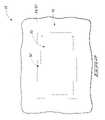
- Substrate 10can be considered as comprising a capacitor array area 25 , a circuitry area 75 other than capacitor array area 25 , and an intervening area 50 between capacitor array area 25 and circuitry area 75 .
- intervening area 50completely surrounds and encircles capacitor array area 25 ( FIG. 2 )
- circuitry area 75comprises a peripheral circuitry area to that of capacitor array area 25 .
- Alternate constructionsare contemplated, of course, for example whereby neither intervening area 50 nor circuitry area 75 completely or partially encircles a capacitor array area 25 .
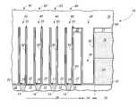
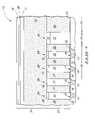
- FIG. 1depicts an insulative material 12 having electrically conductive storage node pillars 14 formed therethrough.
- Materials 12 and 14may be fabricated over some suitable underlying material, for example bulk monocrystalline and/or underlying circuitry.
- Example insulative materials 12include doped and undoped silicon dioxides, for example silicon dioxide deposited by the decomposition of tetraethylorthosilicate (TEOS) and/or borophosphosilicate glass (BPSG) and/or silicon nitride.
- TEOStetraethylorthosilicate
- BPSGborophosphosilicate glass
- silicon nitridesilicon nitride.
- doped silicon dioxideor “silicon dioxide doped” requires at least 0.5 atomic percent concentration of one or a combination of boron or phosphorus in silicon dioxide.
- an undoped silicon dioxiderequires less than 0.5 atomic percent of any of boron and phosphorous.
- material 12might comprise anisotropically etched insulative sidewall spacers, for example formed about transistor gate lines (not shown).
- An example material 14is conductively doped polysilicon. Conductive material 14 can be considered as comprising or defining a plurality of capacitor storage node locations 15 , 16 , 17 and 18 on substrate 10 . Storage node locations 15 , 16 , 17 and 18 are examples only, and regardless, may be conductive at this point in the process, or made conductive subsequently.
- a material 22has been formed over material 12 and capacitor storage node locations 15 , 16 , 17 and 18 .
- Examples for material 22comprise silicon nitride and/or undoped silicon dioxide deposited to an example thickness range of from about 100 Angstroms to about 2,000 Angstroms. Material 22 might be included to provide an etch stop, or other function.
- Some material 24is received over capacitor array area 25 and circuitry area 75 , and also in the depicted embodiment over intervening area 50 .
- Suchmight be homogeneous or comprise multiple different compositions and/or layers.
- An example materialis doped silicon dioxide, for example comprising at least one of phosphorus and boron, such as BPSG, borosilicate glass (BSG), and/or phosphosilicate glass (PSG).
- An example thickness range for material 24is from 5,000 Angstroms to 10 microns, with 2 microns being a specific example. Thinner and greater thicknesses are, of course, contemplated.
- layers 22 and 24comprise example base material 27 received over node locations 15 , 16 , 17 and 18 .
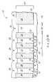
- a plurality of openings 28has been etched into base material 27 over individual node locations 15 , 16 , 17 and 18 . Further, a trench 30 has been formed in intervening area 50 within base material 27 . In one embodiment, trench 30 completely surrounds capacitor area 25 , an example technique for forming capacitor electrode openings 28 and trench 30 comprises photolithographic patterning and selective anisotropic dry etch to produce the example FIGS. 3 and 4 constructions.
- An example minimum width of trench opening 30is from about 200 Angstroms to about 5,000 Angstroms, while an example minimum width for capacitor electrode openings 28 is also from about 200 Angstroms to about 5,000 Angstroms. Trench 30 may or may not be formed at this point in the process, or at all.
- the processing depicted by FIGS. 1-4depicts but one example method of providing a material (i.e. material 27 ) having an opening therein (i.e. any of openings 28 ) over a node location (i.e. any of locations 15 , 16 , 17 and 18 ) on a substrate.
- the opening(s)may or may not extend completely to the node locations at this point in the process.
- the processing depicted by FIGS. 3 and 4can occur in a suitable processing tool which for convenience in description can be considered as a “first processing tool”.
- the first processing toolmay be a plasma etcher.
- a LAMTM ExelanTM oxide etch toolis an example such tool.
- bridging material 32has been formed across base material openings 28 , with such openings 28 comprising voids 33 therebeneath.
- suchoccurs by depositing bridging material 32 over base material 27 and across base material openings 28 , and in one embodiment to partially within base material openings 28 as shown.
- suchoccurs in the very same first processing tool within which the etching to produce openings 28 in FIGS. 3 and 4 occurred, and in one embodiment before removing substrate 10 from such processing tool after such etching to produce openings 28 .
- example bridging materialsinclude nitride-comprising material, for example one or more of silicon nitride, boron nitride, silicon oxynitride, silicon boron nitride, and silicon carbon nitride.
- the bridging materialmight comprise silicon dioxide, including doped and undoped silicon dioxide.
- the base materialcomprises doped silicon dioxide with a nitride received thereover, and silicon dioxide-comprising bridging material received over the nitride of the base material. Such is shown by way of example only with respect to a substrate fragment 10 a in FIG. 6 .
- substrate 10 acomprises a nitride layer 19 (for example any of the above stated nitrides) received over layer 24 as constituting part of base material 27 a .
- nitride layer 19is received “on” (with “on” meaning herein in at least some direct physical touching contact with) layer 24 .
- an outermost portion of material 24comprises doped silicon dioxide and an innermost portion of bridging material 32 comprises undoped silicon dioxide
- undoped silicon dioxide of bridging material 32is formed on doped silicon dioxide of base material 27 .
- Example silicon-containing precursors for chemical or atomic layer depositioninclude SiH 4 , SiCl 4 , SiCl 2 H 2 , and SiF 4 .
- Example nitrogen-containing precursorsinclude NH 3 , NO x , and N 2 .
- An example boron-containing precursoris B 2 H 6 .
- Example carbon-containing precursorsinclude CH 4 , CF 4 , CH 2 F 2 , CHF 3 , CH 3 F, C 4 F 6 , C 4 F 8 , C 2 F 4 , and C 6 .
- Example conditions during deposition within a plasma etcher or a plasma deposition toolinclude a chuck temperature of from 300° C.
- quantity of the atomic components of the composition of bridging material 32can be controlled by quantity of precursor gases depending on the ultimate desired composition of bridging material 32 .
- Bridging material 32might be homogenous or non-homogenous.
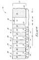
- covering material 34has been formed over those portions of bridging material 32 that are received over base material 27 and across base material openings 28 . Such might be homogenous or non-homogenous, and regardless may comprise multiple layers.
- FIG. 7depicts covering material 34 as comprising four layers 36 , 37 , 38 , and 39 . Any of such materials may be the same or different in composition as one or more components of base material 27 .
- An example material 36is doped silicon dioxide
- an example material 37comprises silicon nitride
- example materials for layers 38 and 39include one or more different organic and/or inorganic antireflective coating layers.
- openings 40have been etched through covering material 34 to bridging material 32 received across openings 28 .
- First capacitor electrodeswill ultimately be formed therein as is described below.
- a trench 42corresponding in general outline to trench 30 , is also shown as having been etched through covering material 34 to bridging material 32 .
- Openings 40 and trench 42are shown as being the same size, shape, and exactly aligned with the respective openings 28 and trench 30 over which such lie. However, such may be of different such size and shape, and regardless may not exactly align over the underlying openings and trench.
- bridging material 32has been etched through, through the covering material openings 40 and 42 .
- the depicted etching of covering material openings 40 in FIG. 8is conducted in a suitable processing tool which for convenience in description can be considered as a “second processing tool”.
- the second processing toolmay be a plasma etcher, for example and by way of example only the LAM Exelan etcher referred to above.
- the FIG. 9 etchingis conducted within the very same processing tool used to form covering material openings 40 in FIG. 8 , and in one embodiment before removing substrate 10 therefrom after etching such covering material openings 40 .
- the second processing toolmay be the very same first processing tool as described above in the one example embodiment where the FIGS. 3 , 4 , and 5 processing occurred in the same processing tool.
- the first and second processing toolsmight be different tools, and whether of the same make and model or of different makes and/or models.
- etching of openings 40 through covering material 34will comprise some suitable etching chemistry which extends the openings to bridging material 32 , for example as is shown in FIG. 8 .
- some suitable etching chemistrywill be used to extend openings 40 to bridging material 32 through the last portion of such covering material 34 , for example through depicted layer 36 .
- Different chemistries and/or etching conditionsmight be used for etching the materials received above layer 36 .
- an example etching chemistry to etch portion 36 and to produce the FIG. 8 constructionincludes a combination of C 4 F 8 , O 2 and Ar.
- the act of etching through bridging material 32 as depicted in FIG. 9comprises continuing, without ceasing, the processing of substrate 10 with the etching chemistry at the conclusion of the etching of openings 40 through covering material 34 as depicted in FIG. 8 effective to etch through bridging material 32 as shown by way of example in FIG. 9 .
- Suchmay can occur in one embodiment when bridging material 32 is of the same or similar composition to that of material 36 , and/or where bridging material 32 is sufficiently thin that punching therethrough can occur without necessarily changing etching chemistry.
- such etchingalso consists essentially of continuing the processing, without ceasing, (for example of the substrate of FIG. 8 ) to produce the example substrate of FIG.
- materials 36 and 32may be of different inherent compositions, but capable of being etched with the same etching chemistry.
- etching of bridging material 32can comprise changing one or more of etching chemistry and etching conditions from those used in etching covering material openings 40 .
- a conductive layer 52for example titanium nitride, has been deposited to within covering material openings 40 and within base material openings 28 in electrical connection with node locations 15 , 16 , 17 and 18 .
- first capacitor electrodes 55are shown as being container in shape, but could of course be of other configurations whether existing or yet-to-be developed, including for example completely plugging the depicted capacitor openings.
- etch access openings 45have been formed through masking layer 37 within capacitor array area 25 effective to expose material 36 of the covering material within capacitor array area 25 . Such leaves elevationally outermost surfaces of material 36 within circuitry area 75 completely covered by masking layer 37 . Etch openings 45 provide access for etchant to subsequently etch materials 36 and 34 within capacitor array area 25 , if such is desired. Alternately by way of example only, it might be decided/desired to not etch material 36 in which event openings 45 might not be formed and masking layer 37 might not be used.
- FIG. 14depicts but one embodiment wherein one of more etching chemistries has etched all of materials 36 , 32 and 24 from within capacitor array area 25 . Alternately, less than all or only some of one or more of materials 36 , 32 and 24 might be etched. Further and regardless, any etching thereof might be conducted dry or with liquid.
- An example liquid etchant solutionis aqueous, and regardless for example comprising HF, where one or more of materials 36 , 32 , and 24 is an oxide.
- One example solutioncomprises 5:1 to 20:1 water to HF by volume, wherein said HF is a 42 weight percent solution of HF in water.
- An example etching temperatureis room ambient, with an example etching pressure also being room ambient.
- An example wet etching chemistry that will etch nitride-comprising materialsincludes H 3 PO 4 .
- etching chemistrymight be changed one or more times to completely remove materials 36 , 32 , and 24 where such removal is desired.
- compositions of material 32 and material 37may be selected to be etchably different and/or of different thicknesses where it is desired that material 37 mask material 36 within periphery circuitry area 75 from being etched.
- FIG. 15illustrates an alternate embodiment to that of FIG. 14 with respect to a substrate fragment 10 b .
- Like numerals from the above described embodimentsare utilized where appropriate, with differences being indicated with different numerals or the suffix “b”.
- bridging material 32remains between adjacent capacitor electrodes 55 .
- Material 24is also shown as having been etched away within array area 25 , but alternately some or all of such may remain. Regardless, bridging material 32 might function as a supporting bracing or lattice structure if such remains in the finished circuitry construction.
- portions of bridging materialmay be etched through to provide etch access to material 24 , for example much like formation of etch openings 45 in layer 37 .
- a capacitor dielectric and a second capacitor electrodeare formed operatively adjacent the first capacitor electrode with respect to individual capacitors.
- FIG. 16depicts the deposition of a capacitor dielectric layer 60 .
- example materialsare silicon dioxide, silicon nitride, silicon dioxide and silicon nitride composite, or any suitable high-k dielectric, and whether existing or yet-to-be developed.
- high-k dielectricsinclude Ta 2 O 5 and barium strontium titanate.
- FIG. 17depicts an example DRAM cell incorporating capacitor 81 .
- Suchcomprises an example transistor gate word line 87 having insulative sidewall spacers, and insulative cap, and a conductive region under the cap such as silicide, a conductive polysilicon region under the silicide, and a gate dielectric region under the polysilicon.
- Source/drain regions 80are shown formed within semiconductive material operatively proximate word line 87 . One of such electrically connects with capacitor 81 , and another of such electrically connects with bitline 85 .
- covering material 34can be etched to expose the nitride-comprising bridging material, with capacitor dielectric 60 and second capacitor electrode 70 being formed thereover.
- capacitor dielectric 60is formed on nitride-comprising bridging material 32 .
- the base material 27may be etched, for example in whole or in part.
- a method of forming a capacitorcomprises providing material having an opening therein over a node location on a substrate.
- a shield comprising nitride-comprising materialis provided within and across the opening, with a void being received within the opening above the shield and a void being received within the opening below the shield.
- FIG. 8is an example such opening if considering a single of one of the covering material openings 40 in combination with a single of one of the base material openings 28 immediately therebelow, with material 32 being provided within and across such opening.
- the space depicted above material 32constitutes one example void received within the opening above a shield, and the space within the opening below shield material 32 constitutes another example void.
- Etchingis conducted within such opening through the shield, with FIG. 9 in but one example depicting an example such etching.
- a first capacitor electrodeis formed within the opening in electrical connection with the node location.
- a capacitor dielectric and a second capacitor electrodeare formed operatively adjacent the first capacitor electrode, for example as described above. Any of the above described processing might be utilized in the context of such a method of forming a capacitor.
Landscapes
- Engineering & Computer Science (AREA)
- Manufacturing & Machinery (AREA)
- Semiconductor Integrated Circuits (AREA)
- Semiconductor Memories (AREA)
Abstract
Description
- Embodiments disclosed herein pertain to methods of forming capacitors.
- Capacitors are one type of component commonly used in the fabrication of integrated circuits, for example in DRAM circuitry. A capacitor is comprised of two conductive electrodes separated by a non-conducting dielectric region. As integrated circuitry density has increased, there is a continuing challenge to maintain sufficiently high storage capacitance despite typical decreasing capacitor area. The increase in density of integrated circuitry has typically resulted in greater reduction in the horizontal dimension of capacitors as compared to the vertical dimension. In many instances, the vertical dimension of capacitors has increased.
- One manner of fabricating capacitors is to initially form an insulative material within which a capacitor storage node electrode is formed. For example, an array of capacitor electrode openings for individual capacitors may be fabricated in such insulative capacitor electrode-forming material, with an example insulative electrode-forming material being silicon dioxide doped with one or both of phosphorus and boron. The capacitor electrode openings may be formed by etching. It can be difficult to etch the capacitor electrode openings within the insulative material, particularly where the openings have high aspect ratio.
- One manner of reducing such difficulty is to split the deposition and etch of such openings into two or more combinations of deposition and etch steps. For example, the material within which the capacitor electrode openings are to be formed can be deposited to an initial deposition thickness which is one half or less of the desired ultimate deposition thickness. Shallower capacitor electrode openings can then be etched to the underlying node location. Such openings are subsequently completely filled/plugged, and another material within which capacitor electrode openings will be formed is deposited over the material in which the first openings were formed and filled. Individual capacitor electrode openings are then formed through the overlying layer to the plugging material. Such can be repeated if desired. Regardless, the plugging material is at some point etched from the capacitor electrode openings to enable contact to be made to a node location on the substrate.
- One common plugging material used in such instances is polysilicon. A native oxide can form on the outermost surfaces thereof that can be difficult to remove. Such oxide can be removed by etching prior to etching the polysilicon within the openings from the substrate. The native oxide etch is usually conducted using an HF wet etching solution. However, the material within which the capacitor electrode openings are usually formed is a doped silicon dioxide, such as borophosphosilicate glass or phosphosilicate glass. The HF will etch such material, thereby undesirably widening the capacitor electrode openings above the plugging material while removing the native oxide received thereover. Further and regardless, it can be difficult to remove the polysilicon plugging material from the openings. Example techniques in accordance with the above are described in U.S. Pat. No. 6,365,453 and 6,204,143.
- Further and regardless, it is often desirable to etch away most if not all of the capacitor electrode-forming material after individual capacitor electrodes have been formed within the openings. Such enables outer sidewall surfaces of the electrodes to provide increased area and thereby increased capacitance for the capacitors being formed. However, the capacitor electrodes formed in deep openings are often correspondingly much taller than they are wide. This can lead to toppling of the capacitor electrodes, either during the etching to expose the outer sidewalls surfaces, during transport of the substrate, and/or during deposition of the capacitor dielectric layer or outer capacitor electrode layer. U.S. Pat. No. 6,667,502 teaches the provision of a brace or retaining structure intended to alleviate such toppling. Other aspects associated in the formation of a plurality of capacitors, some of which include bracing structures, are also disclosed and are:
- U.S. Published Application No. 2005/0051822;
- U.S. Published Application No. 2005/0054159;
- U.S. Published Application No. 2005/0158949;
- U.S. Published Application No. 2005/0287780;
- U.S. Published Application No. 2006/0014344;
- U.S. Published Application No. 2006/0051918;
- U.S. Published Application No. 2006/0046420;
- U.S. Published Application No. 2006/0121672;
- U.S. Published Application No. 2006/0211211;
- U.S. Published Application No. 2006/0263968;
- U.S. Published Application No. 2006/0261440;
- U.S. Published Application No. 2007/0032014;
- U.S. Published Application No. 2006/0063344;
- U.S. Published Application No. 2006/0063345.
- Fabrication of capacitors in integrated circuitry such as memory circuitry may form an array of capacitors within a capacitor array area. Control or other circuitry area is often displaced from the capacitor array area, with the substrate including an intervening area between the capacitor array area and the control or other circuitry area. In some instances, a trench is formed in the intervening area between the capacitor array area and the other circuitry area. Such trench can be formed commensurate with the fabrication of the openings within the capacitor array area within which the isolated capacitor electrodes will be received.
- While the invention was motivated in addressing the above-identified issues, it is no way so limited. The invention is only limited by the accompanying claims as literally worded, and in accordance with the doctrine of equivalence.
FIG. 1 is a diagrammatic cross section of a substrate fragment in process in accordance with an aspect of the invention.FIG. 2 is a diagrammatic top plan view of a larger scale portion of theFIG. 1 substrate.FIG. 3 is a view of theFIG. 1 substrate at a processing step subsequent to that shown byFIG. 1 , and taken through line3-3 inFIG. 4 .FIG. 4 is a diagrammatic top plan view of theFIG. 3 substrate fragment.FIG. 5 is a view of theFIG. 3 substrate at a processing step subsequent to that shown byFIG. 3 .FIG. 6 is a view of an alternate embodiment substrate to that shown byFIG. 5 .FIG. 7 is a view of theFIG. 5 substrate at a processing step subsequent to that shown byFIG. 5 .FIG. 8 is a view of theFIG. 7 substrate at a processing step subsequent to that shown byFIG. 7 .FIG. 9 is a view of theFIG. 8 substrate at a processing step subsequent to that shown byFIG. 8 .FIG. 10 is a view of theFIG. 9 substrate at a processing step subsequent to that shown byFIG. 9 .FIG. 11 is a view of theFIG. 10 substrate at a processing step subsequent to that shown byFIG. 10 .FIG. 12 is a view of theFIG. 11 substrate at a processing step subsequent to that shown byFIG. 11 , and taken through line12-12 inFIG. 13 .FIG. 13 is a diagrammatic top plan view of theFIG. 12 substrate fragment.FIG. 14 is a view of theFIG. 12 substrate at a processing step subsequent to that shown byFIG. 12 .FIG. 15 is a view of an alternate embodiment substrate to that shown byFIG. 14 .FIG. 16 is a view of theFIG. 15 substrate at a processing step subsequent to that shown byFIG. 15 .FIG. 17 is a diagrammatic representation of DRAM circuitry.- Example methods of forming capacitors, including pluralities of capacitors, are described with reference to
FIGS. 1-17 . Referring initially toFIGS. 1 and 2 , a substrate, for example a semiconductor substrate, is indicated generally withreference numeral 10. In the context of this document, the term “semiconductor substrate” or “semiconductive substrate” is defined to mean any construction comprising semiconductive material, including, but not limited to, bulk semiconductive materials such as a semiconductive wafer (either alone or in assemblies comprising other materials thereon), and semiconductive material layers (either alone or in assemblies comprising other materials). The term “substrate” refers to any supporting structure, including, but not limited to, the semiconductive substrates described above. Accordingly, and by way of example only,FIG. 1 might comprise a bulk semiconductor material (not shown), for example bulk monocrystalline, and/or comprise semiconductor-on-insulator layers. Substrate 10 can be considered as comprising acapacitor array area 25, acircuitry area 75 other thancapacitor array area 25, and an interveningarea 50 betweencapacitor array area 25 andcircuitry area 75. In the depicted example embodiment, interveningarea 50 completely surrounds and encircles capacitor array area25 (FIG. 2 ), andcircuitry area 75 comprises a peripheral circuitry area to that ofcapacitor array area 25. Alternate constructions are contemplated, of course, for example whereby neither interveningarea 50 norcircuitry area 75 completely or partially encircles acapacitor array area 25.FIG. 1 depicts aninsulative material 12 having electrically conductivestorage node pillars 14 formed therethrough.Materials Example insulative materials 12 include doped and undoped silicon dioxides, for example silicon dioxide deposited by the decomposition of tetraethylorthosilicate (TEOS) and/or borophosphosilicate glass (BPSG) and/or silicon nitride. In the context of this document, “doped silicon dioxide” or “silicon dioxide doped” requires at least 0.5 atomic percent concentration of one or a combination of boron or phosphorus in silicon dioxide. Further, an undoped silicon dioxide requires less than 0.5 atomic percent of any of boron and phosphorous. Alternately by way of example only,material 12 might comprise anisotropically etched insulative sidewall spacers, for example formed about transistor gate lines (not shown). Anexample material 14 is conductively doped polysilicon.Conductive material 14 can be considered as comprising or defining a plurality of capacitorstorage node locations substrate 10.Storage node locations - A
material 22 has been formed overmaterial 12 and capacitorstorage node locations material 22 comprise silicon nitride and/or undoped silicon dioxide deposited to an example thickness range of from about 100 Angstroms to about 2,000 Angstroms.Material 22 might be included to provide an etch stop, or other function. - Some material24 is received over
capacitor array area 25 andcircuitry area 75, and also in the depicted embodiment over interveningarea 50. Such might be homogeneous or comprise multiple different compositions and/or layers. An example material is doped silicon dioxide, for example comprising at least one of phosphorus and boron, such as BPSG, borosilicate glass (BSG), and/or phosphosilicate glass (PSG). An example thickness range formaterial 24 is from 5,000 Angstroms to 10 microns, with 2 microns being a specific example. Thinner and greater thicknesses are, of course, contemplated. Regardless and in one embodiment, layers22 and24 compriseexample base material 27 received overnode locations - Referring to
FIGS. 3 and 4 , a plurality ofopenings 28 has been etched intobase material 27 overindividual node locations trench 30 has been formed in interveningarea 50 withinbase material 27. In one embodiment,trench 30 completely surroundscapacitor area 25, an example technique for formingcapacitor electrode openings 28 andtrench 30 comprises photolithographic patterning and selective anisotropic dry etch to produce the exampleFIGS. 3 and 4 constructions. An example minimum width oftrench opening 30 is from about 200 Angstroms to about 5,000 Angstroms, while an example minimum width forcapacitor electrode openings 28 is also from about 200 Angstroms to about 5,000 Angstroms.Trench 30 may or may not be formed at this point in the process, or at all. Regardless, the processing depicted byFIGS. 1-4 depicts but one example method of providing a material (i.e. material27) having an opening therein (i.e. any of openings28) over a node location (i.e. any oflocations FIGS. 3 and 4 can occur in a suitable processing tool which for convenience in description can be considered as a “first processing tool”. In one embodiment the first processing tool may be a plasma etcher. By way of example only, a LAM™ Exelan™ oxide etch tool is an example such tool. - Referring to
FIG. 5 , bridgingmaterial 32 has been formed acrossbase material openings 28, withsuch openings 28 comprisingvoids 33 therebeneath. In one embodiment, such occurs by depositing bridgingmaterial 32 overbase material 27 and acrossbase material openings 28, and in one embodiment to partially withinbase material openings 28 as shown. In one embodiment, such occurs in the very same first processing tool within which the etching to produceopenings 28 inFIGS. 3 and 4 occurred, and in one embodiment before removingsubstrate 10 from such processing tool after such etching to produceopenings 28. By way of examples only, example bridging materials include nitride-comprising material, for example one or more of silicon nitride, boron nitride, silicon oxynitride, silicon boron nitride, and silicon carbon nitride. Further additionally or alternately and by way of examples only, the bridging material might comprise silicon dioxide, including doped and undoped silicon dioxide. In one embodiment, the base material comprises doped silicon dioxide with a nitride received thereover, and silicon dioxide-comprising bridging material received over the nitride of the base material. Such is shown by way of example only with respect to a substrate fragment10ainFIG. 6 . Like numerals form the first described embodiment are utilized where appropriate, with differences being indicated with different numerals or the suffix “a”. InFIG. 6 , substrate10acomprises a nitride layer19 (for example any of the above stated nitrides) received overlayer 24 as constituting part of base material27a. In the depicted embodiment, nitride layer19 is received “on” (with “on” meaning herein in at least some direct physical touching contact with)layer 24. In one embodiment, such as shown inFIG. 5 and where an outermost portion ofmaterial 24 comprises doped silicon dioxide and an innermost portion of bridgingmaterial 32 comprises undoped silicon dioxide, undoped silicon dioxide of bridgingmaterial 32 is formed on doped silicon dioxide ofbase material 27. - Regardless, these and/or other materials can be deposited by any existing or yet-to-be developed techniques. Example silicon-containing precursors for chemical or atomic layer deposition include SiH4, SiCl4, SiCl2H2, and SiF4. Example nitrogen-containing precursors include NH3, NOx, and N2. An example boron-containing precursor is B2H6. Example carbon-containing precursors include CH4, CF4, CH2F2, CHF3, CH3F, C4F6, C4F8, C2F4, and C6. Example conditions during deposition within a plasma etcher or a plasma deposition tool include a chuck temperature of from 300° C. to 500° C., pressure from 10 mTorr to 10 Torr, total power of from 500 watts to 2,000 watts and frequencies at one or a combination of 2 MHz and 27 MHz. Regardless, quantity of the atomic components of the composition of bridging
material 32 can be controlled by quantity of precursor gases depending on the ultimate desired composition of bridgingmaterial 32. Bridgingmaterial 32 might be homogenous or non-homogenous. - Referring to
FIG. 7 and in one embodiment, coveringmaterial 34 has been formed over those portions of bridgingmaterial 32 that are received overbase material 27 and acrossbase material openings 28. Such might be homogenous or non-homogenous, and regardless may comprise multiple layers.FIG. 7 depicts coveringmaterial 34 as comprising fourlayers base material 27. Anexample material 36 is doped silicon dioxide, anexample material 37 comprises silicon nitride, and example materials forlayers - Referring to
FIG. 8 ,openings 40 have been etched through coveringmaterial 34 to bridgingmaterial 32 received acrossopenings 28. First capacitor electrodes will ultimately be formed therein as is described below. Atrench 42, corresponding in general outline to trench30, is also shown as having been etched through coveringmaterial 34 to bridgingmaterial 32.Openings 40 andtrench 42 are shown as being the same size, shape, and exactly aligned with therespective openings 28 andtrench 30 over which such lie. However, such may be of different such size and shape, and regardless may not exactly align over the underlying openings and trench. - Referring to
FIG. 9 , bridgingmaterial 32 has been etched through, through the coveringmaterial openings - In one embodiment, the depicted etching of covering
material openings 40 inFIG. 8 is conducted in a suitable processing tool which for convenience in description can be considered as a “second processing tool”. In one embodiment, the second processing tool may be a plasma etcher, for example and by way of example only the LAM Exelan etcher referred to above. Regardless in one embodiment, theFIG. 9 etching is conducted within the very same processing tool used to form coveringmaterial openings 40 inFIG. 8 , and in one embodiment before removingsubstrate 10 therefrom after etching suchcovering material openings 40. In one embodiment, the second processing tool may be the very same first processing tool as described above in the one example embodiment where theFIGS. 3 ,4, and5 processing occurred in the same processing tool. Alternately and by way of example only, the first and second processing tools might be different tools, and whether of the same make and model or of different makes and/or models. - In one embodiment, etching of
openings 40 through coveringmaterial 34 will comprise some suitable etching chemistry which extends the openings to bridgingmaterial 32, for example as is shown inFIG. 8 . Where, for example, coveringmaterial 34 comprises multiple different compositions, some suitable etching chemistry will be used to extendopenings 40 to bridgingmaterial 32 through the last portion ofsuch covering material 34, for example through depictedlayer 36. Different chemistries and/or etching conditions might be used for etching the materials received abovelayer 36. Regardless, whereportion 36 of coveringmaterial 34 comprises PSG, an example etching chemistry to etchportion 36 and to produce theFIG. 8 construction includes a combination of C4F8, O2and Ar. Regardless, in one embodiment, the act of etching through bridgingmaterial 32 as depicted inFIG. 9 comprises continuing, without ceasing, the processing ofsubstrate 10 with the etching chemistry at the conclusion of the etching ofopenings 40 through coveringmaterial 34 as depicted inFIG. 8 effective to etch through bridgingmaterial 32 as shown by way of example inFIG. 9 . Such may can occur in one embodiment when bridgingmaterial 32 is of the same or similar composition to that ofmaterial 36, and/or where bridgingmaterial 32 is sufficiently thin that punching therethrough can occur without necessarily changing etching chemistry. In one embodiment, such etching also consists essentially of continuing the processing, without ceasing, (for example of the substrate ofFIG. 8 ) to produce the example substrate ofFIG. 9 also using the very same etching conditions (meaning the combination of pressure, temperature, and any applied power) that were in use at the conclusion of the etching to produce the exampleFIG. 8 construction. Alternately,materials - Alternately and likely where bridging
material 32 comprises a material etchably different in composition from that ofmaterial 36, etching of bridgingmaterial 32 can comprise changing one or more of etching chemistry and etching conditions from those used in etching coveringmaterial openings 40. - Referring to
FIG. 10 , aconductive layer 52, for example titanium nitride, has been deposited to within coveringmaterial openings 40 and withinbase material openings 28 in electrical connection withnode locations - Referring to
FIG. 11 ,conductive layer 52 and layers38 and39 have been etched or polished back tolayer 37. Such provides, by way of example only, one manner of forming respectivefirst capacitor electrodes 55 within coveringmaterial openings 40 and within the base material openings in electrical connection withnode locations first capacitor electrodes 55 are shown as being container in shape, but could of course be of other configurations whether existing or yet-to-be developed, including for example completely plugging the depicted capacitor openings. - Referring to
FIGS. 12 and 13 ,etch access openings 45 have been formed throughmasking layer 37 withincapacitor array area 25 effective to exposematerial 36 of the covering material withincapacitor array area 25. Such leaves elevationally outermost surfaces ofmaterial 36 withincircuitry area 75 completely covered by maskinglayer 37.Etch openings 45 provide access for etchant to subsequently etchmaterials capacitor array area 25, if such is desired. Alternately by way of example only, it might be decided/desired to not etchmaterial 36 in whichevent openings 45 might not be formed andmasking layer 37 might not be used. - Referring to
FIG. 14 ,materials capacitor array area 25 have been etched, for example with a liquid etching solution.FIG. 14 depicts but one embodiment wherein one of more etching chemistries has etched all ofmaterials capacitor array area 25. Alternately, less than all or only some of one or more ofmaterials materials example materials material 32 is predominantly silicon nitride-comprising, etching chemistry might be changed one or more times to completely removematerials material 32 andmaterial 37 may be selected to be etchably different and/or of different thicknesses where it is desired thatmaterial 37mask material 36 withinperiphery circuitry area 75 from being etched. FIG. 15 illustrates an alternate embodiment to that ofFIG. 14 with respect to a substrate fragment10b. Like numerals from the above described embodiments are utilized where appropriate, with differences being indicated with different numerals or the suffix “b”. InFIG. 15 , at least some of bridgingmaterial 32 remains betweenadjacent capacitor electrodes 55.Material 24 is also shown as having been etched away withinarray area 25, but alternately some or all of such may remain. Regardless, bridgingmaterial 32 might function as a supporting bracing or lattice structure if such remains in the finished circuitry construction. Where it is desired to keep some or all of bridgingmaterial 32 and remove some or all ofmaterial 24 withinarray area 25, portions of bridging material may be etched through to provide etch access tomaterial 24, for example much like formation ofetch openings 45 inlayer 37.- Referring to
FIG. 16 , a capacitor dielectric and a second capacitor electrode are formed operatively adjacent the first capacitor electrode with respect to individual capacitors. For example and by way of example only,FIG. 16 depicts the deposition of acapacitor dielectric layer 60. By way of example only, example materials are silicon dioxide, silicon nitride, silicon dioxide and silicon nitride composite, or any suitable high-k dielectric, and whether existing or yet-to-be developed. By way of example only, high-k dielectrics include Ta2O5and barium strontium titanate. - An outer
capacitor electrode layer 70 has been deposited overcapacitor dielectric layer 60, thereby definingcapacitors FIG. 17 depicts an example DRAMcell incorporating capacitor 81. Such comprises an example transistorgate word line 87 having insulative sidewall spacers, and insulative cap, and a conductive region under the cap such as silicide, a conductive polysilicon region under the silicide, and a gate dielectric region under the polysilicon. Source/drain regions 80 are shown formed within semiconductive material operativelyproximate word line 87. One of such electrically connects withcapacitor 81, and another of such electrically connects withbitline 85. - Regardless and by way of example only, in one embodiment where bridging
material 32 comprises nitride, coveringmaterial 34 can be etched to expose the nitride-comprising bridging material, withcapacitor dielectric 60 andsecond capacitor electrode 70 being formed thereover. In one embodiment and as shown,capacitor dielectric 60 is formed on nitride-comprisingbridging material 32. Regardless in one embodiment, after etching coveringmaterial 34 to expose nitride-comprisingbridging material 32 received overbase material 27 and before formingcapacitor dielectric 60 andsecond capacitor electrode 70, thebase material 27 may be etched, for example in whole or in part. - In one embodiment, a method of forming a capacitor comprises providing material having an opening therein over a node location on a substrate. A shield comprising nitride-comprising material is provided within and across the opening, with a void being received within the opening above the shield and a void being received within the opening below the shield. By way of example only,
FIG. 8 is an example such opening if considering a single of one of the coveringmaterial openings 40 in combination with a single of one of thebase material openings 28 immediately therebelow, withmaterial 32 being provided within and across such opening. The space depicted abovematerial 32 constitutes one example void received within the opening above a shield, and the space within the opening belowshield material 32 constitutes another example void. - Etching is conducted within such opening through the shield, with
FIG. 9 in but one example depicting an example such etching. After such etching, a first capacitor electrode is formed within the opening in electrical connection with the node location. A capacitor dielectric and a second capacitor electrode are formed operatively adjacent the first capacitor electrode, for example as described above. Any of the above described processing might be utilized in the context of such a method of forming a capacitor. - In compliance with the statute, the subject matter disclosed herein has been described in language more or less specific as to structural and methodical features. It is to be understood, however, that the claims are not limited to the specific features shown and described, since the means herein disclosed comprise example embodiments. The claims are thus to be afforded full scope as literally worded, and to be appropriately interpreted in accordance with the doctrine of equivalents.
Claims (29)
Priority Applications (2)
| Application Number | Priority Date | Filing Date | Title |
|---|---|---|---|
| US12/114,124US7618874B1 (en) | 2008-05-02 | 2008-05-02 | Methods of forming capacitors |
| US12/575,263US8318578B2 (en) | 2008-05-02 | 2009-10-07 | Method of forming capacitors |
Applications Claiming Priority (1)
| Application Number | Priority Date | Filing Date | Title |
|---|---|---|---|
| US12/114,124US7618874B1 (en) | 2008-05-02 | 2008-05-02 | Methods of forming capacitors |
Related Child Applications (1)
| Application Number | Title | Priority Date | Filing Date |
|---|---|---|---|
| US12/575,263ContinuationUS8318578B2 (en) | 2008-05-02 | 2009-10-07 | Method of forming capacitors |
Publications (2)
| Publication Number | Publication Date |
|---|---|
| US20090275185A1true US20090275185A1 (en) | 2009-11-05 |
| US7618874B1 US7618874B1 (en) | 2009-11-17 |
Family
ID=41257382
Family Applications (2)
| Application Number | Title | Priority Date | Filing Date |
|---|---|---|---|
| US12/114,124ActiveUS7618874B1 (en) | 2008-05-02 | 2008-05-02 | Methods of forming capacitors |
| US12/575,263Active2029-09-14US8318578B2 (en) | 2008-05-02 | 2009-10-07 | Method of forming capacitors |
Family Applications After (1)
| Application Number | Title | Priority Date | Filing Date |
|---|---|---|---|
| US12/575,263Active2029-09-14US8318578B2 (en) | 2008-05-02 | 2009-10-07 | Method of forming capacitors |
Country Status (1)
| Country | Link |
|---|---|
| US (2) | US7618874B1 (en) |
Cited By (7)
| Publication number | Priority date | Publication date | Assignee | Title |
|---|---|---|---|---|
| US20100041204A1 (en)* | 2008-08-13 | 2010-02-18 | Mark Kiehlbauch | Methods Of Making Capacitors, DRAM Arrays and Electronic Systems |
| US20100159663A1 (en)* | 2008-12-23 | 2010-06-24 | Hynix Semiconductor Inc. | Method of fabricating high integrated semiconductor apparatus, and semiconductor apparatus fabricated thereby |
| CN102103984A (en)* | 2009-12-17 | 2011-06-22 | 南亚科技股份有限公司 | Stacked capacitor of memory element and manufacturing method thereof |
| US8274777B2 (en) | 2008-04-08 | 2012-09-25 | Micron Technology, Inc. | High aspect ratio openings |
| US10964475B2 (en)* | 2019-01-28 | 2021-03-30 | Micron Technology, Inc. | Formation of a capacitor using a sacrificial layer |
| US20220085151A1 (en)* | 2020-09-11 | 2022-03-17 | Changxin Memory Technologies, Inc. | Semiconductor structure and method for manufacturing semiconductor structure |
| US20220085152A1 (en)* | 2020-09-11 | 2022-03-17 | Changxin Memory Technologies, Inc. | Semiconductor structure and method for manufacturing semiconductor structure |
Families Citing this family (5)
| Publication number | Priority date | Publication date | Assignee | Title |
|---|---|---|---|---|
| US7666797B2 (en)* | 2006-08-17 | 2010-02-23 | Micron Technology, Inc. | Methods for forming semiconductor constructions, and methods for selectively etching silicon nitride relative to conductive material |
| US7618874B1 (en)* | 2008-05-02 | 2009-11-17 | Micron Technology, Inc. | Methods of forming capacitors |
| US7696056B2 (en)* | 2008-05-02 | 2010-04-13 | Micron Technology, Inc. | Methods of forming capacitors |
| WO2012047220A1 (en) | 2010-10-07 | 2012-04-12 | Empire Technology Development Llc | Data transmission through optical vias |
| US8921977B2 (en)* | 2011-12-21 | 2014-12-30 | Nan Ya Technology Corporation | Capacitor array and method of fabricating the same |
Citations (27)
| Publication number | Priority date | Publication date | Assignee | Title |
|---|---|---|---|---|
| US5874335A (en)* | 1997-12-12 | 1999-02-23 | United Microelectronics Corp. | Method of fabricating DRAM capacitors |
| US5998259A (en)* | 1998-03-20 | 1999-12-07 | United Semiconductor Corp. | Method of fabricating dual cylindrical capacitor |
| US6037216A (en)* | 1998-11-02 | 2000-03-14 | Vanguard International Semiconductor Corporation | Method for simultaneously fabricating capacitor structures, for giga-bit DRAM cells, and peripheral interconnect structures, using a dual damascene process |
| US6130102A (en)* | 1997-11-03 | 2000-10-10 | Motorola Inc. | Method for forming semiconductor device including a dual inlaid structure |
| US6146962A (en)* | 1998-03-17 | 2000-11-14 | National Semiconductor Corporation | Method for forming a DRAM cell with a stacked capacitor |
| US6174781B1 (en)* | 1999-04-26 | 2001-01-16 | Worldwide Semiconductor Manufacturing Corp. | Dual damascene process for capacitance fabrication of DRAM |
| US20010018124A1 (en)* | 1997-05-22 | 2001-08-30 | Kimio Yamakawa | Semiconductor devices |
| US6300235B1 (en)* | 1997-06-30 | 2001-10-09 | Siemens Aktiengesellschaft | Method of forming multi-level coplanar metal/insulator films using dual damascene with sacrificial flowable oxide |
| US20020149044A1 (en)* | 1997-10-14 | 2002-10-17 | Naruhiko Nakanishi | Semiconductor integrated circuit device and method of manufacturing the same |
| US6630380B1 (en)* | 2002-09-30 | 2003-10-07 | Chartered Semiconductor Manufacturing Ltd | Method for making three-dimensional metal-insulator-metal capacitors for dynamic random access memory (DRAM) and ferroelectric random access memory (FERAM) |
| US20040135182A1 (en)* | 2002-11-11 | 2004-07-15 | Hyeong-Geun An | Ferroelectric capacitors including a seed conductive film and methods for manufacturing the same |
| US20040147074A1 (en)* | 2001-02-26 | 2004-07-29 | Bernhard Sell | Method for fabricating a storage capacitor |
| US20050030697A1 (en)* | 1997-08-04 | 2005-02-10 | Micron Technology, Inc. | Capacitor structure |
| US20050088895A1 (en)* | 2003-07-25 | 2005-04-28 | Infineon Technologies Ag | DRAM cell array having vertical memory cells and methods for fabricating a DRAM cell array and a DRAM |
| US7009232B2 (en)* | 1995-09-20 | 2006-03-07 | Micron Technology, Inc. | Semiconductor memory circuitry including die sites sized for 256M to 275M memory cells in an 8-inch wafer |
| US20060138516A1 (en)* | 2004-12-27 | 2006-06-29 | Samsung Electronics Co., Ltd. | Method of forming DRAM device having capacitor and DRAM device so formed |
| US20060211178A1 (en)* | 2004-02-10 | 2006-09-21 | Kim Dae-Hwan | Fabrication of lean-free stacked capacitors |
| US20070001208A1 (en)* | 2005-06-30 | 2007-01-04 | Andrew Graham | DRAM having carbon stack capacitor |
| US20070026540A1 (en)* | 2005-03-15 | 2007-02-01 | Nooten Sebastian E V | Method of forming non-conformal layers |
| US20070111606A1 (en)* | 2004-09-03 | 2007-05-17 | Staktek Group L.P., A Texas Limited Partnership | Buffered Thin Module System and Method |
| US7229895B2 (en)* | 2005-01-14 | 2007-06-12 | Micron Technology, Inc | Memory array buried digit line |
| US20070173014A1 (en)* | 2005-05-05 | 2007-07-26 | Manning H M | Method for forming memory cell and device |
| US20070207622A1 (en)* | 2006-02-23 | 2007-09-06 | Micron Technology, Inc. | Highly selective doped oxide etchant |
| US20070238259A1 (en)* | 2006-04-10 | 2007-10-11 | Micron Technology, Inc. | Methods of forming a plurality of capacitors |
| US7285812B2 (en)* | 2004-09-02 | 2007-10-23 | Micron Technology, Inc. | Vertical transistors |
| US7326656B2 (en)* | 2004-09-30 | 2008-02-05 | Intel Corporation | Method of forming a metal oxide dielectric |
| US7465680B2 (en)* | 2005-09-07 | 2008-12-16 | Applied Materials, Inc. | Post deposition plasma treatment to increase tensile stress of HDP-CVD SIO2 |
Family Cites Families (12)
| Publication number | Priority date | Publication date | Assignee | Title |
|---|---|---|---|---|
| TW382772B (en) | 1996-10-03 | 2000-02-21 | Vanguard Int Semiconduct Corp | Method for making DRAM cell with dual-crown capacitor using polysilicon and nitride spacer |
| TW427002B (en) | 1999-01-28 | 2001-03-21 | United Microelectronics Corp | Manufacturing method of DRAM capacitor |
| TW417292B (en) | 1999-02-19 | 2001-01-01 | Taiwan Semiconductor Mfg | Method for forming HSG-polysilicon DRAM capacitor by using dual nitride layers |
| TW416140B (en) | 1999-03-09 | 2000-12-21 | Vanguard Int Semiconduct Corp | Using dual-damascene method to simultaneously produce the capacitor structure and its peripheral interconnect structure of dynamic random access memory unit |
| TW423148B (en) | 1999-05-13 | 2001-02-21 | Taiwan Semiconductor Mfg | Manufacturing method of dual crown-type rough poly-silicon DRAM capacitor |
| US6403442B1 (en)* | 1999-09-02 | 2002-06-11 | Micron Technology, Inc. | Methods of forming capacitors and resultant capacitor structures |
| US6967147B1 (en) | 2000-11-16 | 2005-11-22 | Infineon Technologies Ag | Nitrogen implantation using a shadow effect to control gate oxide thickness in DRAM semiconductor |
| KR100400246B1 (en) | 2000-12-29 | 2003-10-01 | 주식회사 하이닉스반도체 | Method for forming of capacitor the cell used high-integrated DRAM |
| DE10219123B4 (en)* | 2002-04-29 | 2004-06-03 | Infineon Technologies Ag | Process for structuring ceramic layers on semiconductor substances with uneven topography |
| KR100449256B1 (en) | 2002-11-28 | 2004-09-18 | 주식회사 하이닉스반도체 | Method for forming the DRAM memory cell |
| US7618874B1 (en)* | 2008-05-02 | 2009-11-17 | Micron Technology, Inc. | Methods of forming capacitors |
| US7696056B2 (en)* | 2008-05-02 | 2010-04-13 | Micron Technology, Inc. | Methods of forming capacitors |
- 2008
- 2008-05-02USUS12/114,124patent/US7618874B1/enactiveActive
- 2009
- 2009-10-07USUS12/575,263patent/US8318578B2/enactiveActive
Patent Citations (27)
| Publication number | Priority date | Publication date | Assignee | Title |
|---|---|---|---|---|
| US7009232B2 (en)* | 1995-09-20 | 2006-03-07 | Micron Technology, Inc. | Semiconductor memory circuitry including die sites sized for 256M to 275M memory cells in an 8-inch wafer |
| US20010018124A1 (en)* | 1997-05-22 | 2001-08-30 | Kimio Yamakawa | Semiconductor devices |
| US6300235B1 (en)* | 1997-06-30 | 2001-10-09 | Siemens Aktiengesellschaft | Method of forming multi-level coplanar metal/insulator films using dual damascene with sacrificial flowable oxide |
| US20050030697A1 (en)* | 1997-08-04 | 2005-02-10 | Micron Technology, Inc. | Capacitor structure |
| US20020149044A1 (en)* | 1997-10-14 | 2002-10-17 | Naruhiko Nakanishi | Semiconductor integrated circuit device and method of manufacturing the same |
| US6130102A (en)* | 1997-11-03 | 2000-10-10 | Motorola Inc. | Method for forming semiconductor device including a dual inlaid structure |
| US5874335A (en)* | 1997-12-12 | 1999-02-23 | United Microelectronics Corp. | Method of fabricating DRAM capacitors |
| US6146962A (en)* | 1998-03-17 | 2000-11-14 | National Semiconductor Corporation | Method for forming a DRAM cell with a stacked capacitor |
| US5998259A (en)* | 1998-03-20 | 1999-12-07 | United Semiconductor Corp. | Method of fabricating dual cylindrical capacitor |
| US6037216A (en)* | 1998-11-02 | 2000-03-14 | Vanguard International Semiconductor Corporation | Method for simultaneously fabricating capacitor structures, for giga-bit DRAM cells, and peripheral interconnect structures, using a dual damascene process |
| US6174781B1 (en)* | 1999-04-26 | 2001-01-16 | Worldwide Semiconductor Manufacturing Corp. | Dual damascene process for capacitance fabrication of DRAM |
| US20040147074A1 (en)* | 2001-02-26 | 2004-07-29 | Bernhard Sell | Method for fabricating a storage capacitor |
| US6630380B1 (en)* | 2002-09-30 | 2003-10-07 | Chartered Semiconductor Manufacturing Ltd | Method for making three-dimensional metal-insulator-metal capacitors for dynamic random access memory (DRAM) and ferroelectric random access memory (FERAM) |
| US20040135182A1 (en)* | 2002-11-11 | 2004-07-15 | Hyeong-Geun An | Ferroelectric capacitors including a seed conductive film and methods for manufacturing the same |
| US20050088895A1 (en)* | 2003-07-25 | 2005-04-28 | Infineon Technologies Ag | DRAM cell array having vertical memory cells and methods for fabricating a DRAM cell array and a DRAM |
| US20060211178A1 (en)* | 2004-02-10 | 2006-09-21 | Kim Dae-Hwan | Fabrication of lean-free stacked capacitors |
| US7285812B2 (en)* | 2004-09-02 | 2007-10-23 | Micron Technology, Inc. | Vertical transistors |
| US20070111606A1 (en)* | 2004-09-03 | 2007-05-17 | Staktek Group L.P., A Texas Limited Partnership | Buffered Thin Module System and Method |
| US7326656B2 (en)* | 2004-09-30 | 2008-02-05 | Intel Corporation | Method of forming a metal oxide dielectric |
| US20060138516A1 (en)* | 2004-12-27 | 2006-06-29 | Samsung Electronics Co., Ltd. | Method of forming DRAM device having capacitor and DRAM device so formed |
| US7229895B2 (en)* | 2005-01-14 | 2007-06-12 | Micron Technology, Inc | Memory array buried digit line |
| US20070026540A1 (en)* | 2005-03-15 | 2007-02-01 | Nooten Sebastian E V | Method of forming non-conformal layers |
| US20070173014A1 (en)* | 2005-05-05 | 2007-07-26 | Manning H M | Method for forming memory cell and device |
| US20070001208A1 (en)* | 2005-06-30 | 2007-01-04 | Andrew Graham | DRAM having carbon stack capacitor |
| US7465680B2 (en)* | 2005-09-07 | 2008-12-16 | Applied Materials, Inc. | Post deposition plasma treatment to increase tensile stress of HDP-CVD SIO2 |
| US20070207622A1 (en)* | 2006-02-23 | 2007-09-06 | Micron Technology, Inc. | Highly selective doped oxide etchant |
| US20070238259A1 (en)* | 2006-04-10 | 2007-10-11 | Micron Technology, Inc. | Methods of forming a plurality of capacitors |
Cited By (14)
| Publication number | Priority date | Publication date | Assignee | Title |
|---|---|---|---|---|
| US9595387B2 (en) | 2008-04-08 | 2017-03-14 | Micron Technology, Inc. | High aspect ratio openings |
| US8274777B2 (en) | 2008-04-08 | 2012-09-25 | Micron Technology, Inc. | High aspect ratio openings |
| US8760841B2 (en) | 2008-04-08 | 2014-06-24 | Micron Technology, Inc. | High aspect ratio openings |
| US20100041204A1 (en)* | 2008-08-13 | 2010-02-18 | Mark Kiehlbauch | Methods Of Making Capacitors, DRAM Arrays and Electronic Systems |
| US8268695B2 (en) | 2008-08-13 | 2012-09-18 | Micron Technology, Inc. | Methods of making capacitors |
| US8853050B2 (en) | 2008-08-13 | 2014-10-07 | Micron Technology | Methods of forming capacitors |
| US20100159663A1 (en)* | 2008-12-23 | 2010-06-24 | Hynix Semiconductor Inc. | Method of fabricating high integrated semiconductor apparatus, and semiconductor apparatus fabricated thereby |
| US7776702B2 (en)* | 2008-12-23 | 2010-08-17 | Hynix Semiconductor Inc | Method of fabricating high integrated semiconductor apparatus, and semiconductor apparatus fabricated thereby |
| CN102103984A (en)* | 2009-12-17 | 2011-06-22 | 南亚科技股份有限公司 | Stacked capacitor of memory element and manufacturing method thereof |
| US10964475B2 (en)* | 2019-01-28 | 2021-03-30 | Micron Technology, Inc. | Formation of a capacitor using a sacrificial layer |
| US20220085151A1 (en)* | 2020-09-11 | 2022-03-17 | Changxin Memory Technologies, Inc. | Semiconductor structure and method for manufacturing semiconductor structure |
| US20220085152A1 (en)* | 2020-09-11 | 2022-03-17 | Changxin Memory Technologies, Inc. | Semiconductor structure and method for manufacturing semiconductor structure |
| US11901405B2 (en)* | 2020-09-11 | 2024-02-13 | Changxin Memory Technologies, Inc. | Semiconductor structure and method for manufacturing semiconductor structure |
| US11955511B2 (en)* | 2020-09-11 | 2024-04-09 | Changxin Memory Technologies, Inc. | Semiconductor structure and method for manufacturing semiconductor structure |
Also Published As
| Publication number | Publication date |
|---|---|
| US8318578B2 (en) | 2012-11-27 |
| US20100025362A1 (en) | 2010-02-04 |
| US7618874B1 (en) | 2009-11-17 |
Similar Documents
| Publication | Publication Date | Title |
|---|---|---|
| US7618874B1 (en) | Methods of forming capacitors | |
| US7696056B2 (en) | Methods of forming capacitors | |
| US7682924B2 (en) | Methods of forming a plurality of capacitors | |
| US7759193B2 (en) | Methods of forming a plurality of capacitors | |
| US7557013B2 (en) | Methods of forming a plurality of capacitors | |
| US7544563B2 (en) | Methods of forming a plurality of capacitors | |
| US8129240B2 (en) | Methods of forming a plurality of capacitors | |
| KR100539268B1 (en) | Method of manufacturing semiconductor memory device | |
| US9076757B2 (en) | Methods of forming a plurality of capacitors | |
| US7396772B2 (en) | Method for fabricating semiconductor device having capacitor | |
| US20110294276A1 (en) | Method of manufacturing semiconductor device | |
| US5508223A (en) | Method for manufacturing DRAM cell with fork-shaped capacitor | |
| US6548349B2 (en) | Method for fabricating a cylinder-type capacitor for a semiconductor device | |
| US5909621A (en) | Single-side corrugated cylindrical capacitor structure of high density DRAMs | |
| US8728887B2 (en) | Method for fabricating capacitor of semiconductor device | |
| US20100155802A1 (en) | Semiconductor device and method of forming semiconductor device | |
| KR19990078288A (en) | Manufacturing method of cylindrical stacked electrode | |
| KR20130037519A (en) | Capacitor and method of manufacturing the same | |
| US20080132076A1 (en) | Method for avoiding polysilicon defect | |
| KR20040039592A (en) | Method of manufacturing a capacitor of a semiconductor device | |
| KR20020042192A (en) | Method for forming capacitor | |
| KR20050001189A (en) | Method for fabricating capacitor of semiconductor device | |
| KR20060075369A (en) | A method of manufacturing a semiconductor memory device having a capacitor of cylindrical structure |
Legal Events
| Date | Code | Title | Description |
|---|---|---|---|
| AS | Assignment | Owner name:MICRON TECHNOLOGY, INC., IDAHO Free format text:ASSIGNMENT OF ASSIGNORS INTEREST;ASSIGNORS:SHEA, KEVIN;BUSCH, BRETT;GOOD, FARRELL;AND OTHERS;REEL/FRAME:020892/0968;SIGNING DATES FROM 20080416 TO 20080418 | |
| FEPP | Fee payment procedure | Free format text:PAYOR NUMBER ASSIGNED (ORIGINAL EVENT CODE: ASPN); ENTITY STATUS OF PATENT OWNER: LARGE ENTITY | |
| STCF | Information on status: patent grant | Free format text:PATENTED CASE | |
| FPAY | Fee payment | Year of fee payment:4 | |
| AS | Assignment | Owner name:U.S. BANK NATIONAL ASSOCIATION, AS COLLATERAL AGENT, CALIFORNIA Free format text:SECURITY INTEREST;ASSIGNOR:MICRON TECHNOLOGY, INC.;REEL/FRAME:038669/0001 Effective date:20160426 Owner name:U.S. BANK NATIONAL ASSOCIATION, AS COLLATERAL AGEN Free format text:SECURITY INTEREST;ASSIGNOR:MICRON TECHNOLOGY, INC.;REEL/FRAME:038669/0001 Effective date:20160426 | |
| AS | Assignment | Owner name:MORGAN STANLEY SENIOR FUNDING, INC., AS COLLATERAL AGENT, MARYLAND Free format text:PATENT SECURITY AGREEMENT;ASSIGNOR:MICRON TECHNOLOGY, INC.;REEL/FRAME:038954/0001 Effective date:20160426 Owner name:MORGAN STANLEY SENIOR FUNDING, INC., AS COLLATERAL Free format text:PATENT SECURITY AGREEMENT;ASSIGNOR:MICRON TECHNOLOGY, INC.;REEL/FRAME:038954/0001 Effective date:20160426 | |
| FPAY | Fee payment | Year of fee payment:8 | |
| AS | Assignment | Owner name:U.S. BANK NATIONAL ASSOCIATION, AS COLLATERAL AGENT, CALIFORNIA Free format text:CORRECTIVE ASSIGNMENT TO CORRECT THE REPLACE ERRONEOUSLY FILED PATENT #7358718 WITH THE CORRECT PATENT #7358178 PREVIOUSLY RECORDED ON REEL 038669 FRAME 0001. ASSIGNOR(S) HEREBY CONFIRMS THE SECURITY INTEREST;ASSIGNOR:MICRON TECHNOLOGY, INC.;REEL/FRAME:043079/0001 Effective date:20160426 Owner name:U.S. BANK NATIONAL ASSOCIATION, AS COLLATERAL AGEN Free format text:CORRECTIVE ASSIGNMENT TO CORRECT THE REPLACE ERRONEOUSLY FILED PATENT #7358718 WITH THE CORRECT PATENT #7358178 PREVIOUSLY RECORDED ON REEL 038669 FRAME 0001. ASSIGNOR(S) HEREBY CONFIRMS THE SECURITY INTEREST;ASSIGNOR:MICRON TECHNOLOGY, INC.;REEL/FRAME:043079/0001 Effective date:20160426 | |
| AS | Assignment | Owner name:JPMORGAN CHASE BANK, N.A., AS COLLATERAL AGENT, ILLINOIS Free format text:SECURITY INTEREST;ASSIGNORS:MICRON TECHNOLOGY, INC.;MICRON SEMICONDUCTOR PRODUCTS, INC.;REEL/FRAME:047540/0001 Effective date:20180703 Owner name:JPMORGAN CHASE BANK, N.A., AS COLLATERAL AGENT, IL Free format text:SECURITY INTEREST;ASSIGNORS:MICRON TECHNOLOGY, INC.;MICRON SEMICONDUCTOR PRODUCTS, INC.;REEL/FRAME:047540/0001 Effective date:20180703 | |
| AS | Assignment | Owner name:MICRON TECHNOLOGY, INC., IDAHO Free format text:RELEASE BY SECURED PARTY;ASSIGNOR:U.S. BANK NATIONAL ASSOCIATION, AS COLLATERAL AGENT;REEL/FRAME:047243/0001 Effective date:20180629 | |
| AS | Assignment | Owner name:MICRON TECHNOLOGY, INC., IDAHO Free format text:RELEASE BY SECURED PARTY;ASSIGNOR:MORGAN STANLEY SENIOR FUNDING, INC., AS COLLATERAL AGENT;REEL/FRAME:050937/0001 Effective date:20190731 | |
| AS | Assignment | Owner name:MICRON SEMICONDUCTOR PRODUCTS, INC., IDAHO Free format text:RELEASE BY SECURED PARTY;ASSIGNOR:JPMORGAN CHASE BANK, N.A., AS COLLATERAL AGENT;REEL/FRAME:051028/0001 Effective date:20190731 Owner name:MICRON TECHNOLOGY, INC., IDAHO Free format text:RELEASE BY SECURED PARTY;ASSIGNOR:JPMORGAN CHASE BANK, N.A., AS COLLATERAL AGENT;REEL/FRAME:051028/0001 Effective date:20190731 | |
| MAFP | Maintenance fee payment | Free format text:PAYMENT OF MAINTENANCE FEE, 12TH YEAR, LARGE ENTITY (ORIGINAL EVENT CODE: M1553); ENTITY STATUS OF PATENT OWNER: LARGE ENTITY Year of fee payment:12 |