US20090271758A1 - Methods for forming arrays of small, closely spaced features - Google Patents
Methods for forming arrays of small, closely spaced featuresDownload PDFInfo
- Publication number
- US20090271758A1 US20090271758A1US12/498,951US49895109AUS2009271758A1US 20090271758 A1US20090271758 A1US 20090271758A1US 49895109 AUS49895109 AUS 49895109AUS 2009271758 A1US2009271758 A1US 2009271758A1
- Authority
- US
- United States
- Prior art keywords
- lines
- grid
- pillars
- sidewalls
- pattern
- Prior art date
- Legal status (The legal status is an assumption and is not a legal conclusion. Google has not performed a legal analysis and makes no representation as to the accuracy of the status listed.)
- Granted
Links
Images


Classifications
- H—ELECTRICITY
- H10—SEMICONDUCTOR DEVICES; ELECTRIC SOLID-STATE DEVICES NOT OTHERWISE PROVIDED FOR
- H10B—ELECTRONIC MEMORY DEVICES
- H10B20/00—Read-only memory [ROM] devices
- H10B20/20—Programmable ROM [PROM] devices comprising field-effect components
- H—ELECTRICITY
- H10—SEMICONDUCTOR DEVICES; ELECTRIC SOLID-STATE DEVICES NOT OTHERWISE PROVIDED FOR
- H10N—ELECTRIC SOLID-STATE DEVICES NOT OTHERWISE PROVIDED FOR
- H10N70/00—Solid-state devices having no potential barriers, and specially adapted for rectifying, amplifying, oscillating or switching
- H10N70/011—Manufacture or treatment of multistable switching devices
- H10N70/061—Shaping switching materials
- H10N70/068—Shaping switching materials by processes specially adapted for achieving sub-lithographic dimensions, e.g. using spacers
- H—ELECTRICITY
- H01—ELECTRIC ELEMENTS
- H01L—SEMICONDUCTOR DEVICES NOT COVERED BY CLASS H10
- H01L21/00—Processes or apparatus adapted for the manufacture or treatment of semiconductor or solid state devices or of parts thereof
- H01L21/02—Manufacture or treatment of semiconductor devices or of parts thereof
- H01L21/027—Making masks on semiconductor bodies for further photolithographic processing not provided for in group H01L21/18 or H01L21/34
- H01L21/033—Making masks on semiconductor bodies for further photolithographic processing not provided for in group H01L21/18 or H01L21/34 comprising inorganic layers
- H01L21/0334—Making masks on semiconductor bodies for further photolithographic processing not provided for in group H01L21/18 or H01L21/34 comprising inorganic layers characterised by their size, orientation, disposition, behaviour, shape, in horizontal or vertical plane
- H01L21/0337—Making masks on semiconductor bodies for further photolithographic processing not provided for in group H01L21/18 or H01L21/34 comprising inorganic layers characterised by their size, orientation, disposition, behaviour, shape, in horizontal or vertical plane characterised by the process involved to create the mask, e.g. lift-off masks, sidewalls, or to modify the mask, e.g. pre-treatment, post-treatment
- H—ELECTRICITY
- H01—ELECTRIC ELEMENTS
- H01L—SEMICONDUCTOR DEVICES NOT COVERED BY CLASS H10
- H01L21/00—Processes or apparatus adapted for the manufacture or treatment of semiconductor or solid state devices or of parts thereof
- H01L21/02—Manufacture or treatment of semiconductor devices or of parts thereof
- H01L21/04—Manufacture or treatment of semiconductor devices or of parts thereof the devices having potential barriers, e.g. a PN junction, depletion layer or carrier concentration layer
- H01L21/18—Manufacture or treatment of semiconductor devices or of parts thereof the devices having potential barriers, e.g. a PN junction, depletion layer or carrier concentration layer the devices having semiconductor bodies comprising elements of Group IV of the Periodic Table or AIIIBV compounds with or without impurities, e.g. doping materials
- H01L21/30—Treatment of semiconductor bodies using processes or apparatus not provided for in groups H01L21/20 - H01L21/26
- H01L21/31—Treatment of semiconductor bodies using processes or apparatus not provided for in groups H01L21/20 - H01L21/26 to form insulating layers thereon, e.g. for masking or by using photolithographic techniques; After treatment of these layers; Selection of materials for these layers
- H01L21/3105—After-treatment
- H01L21/311—Etching the insulating layers by chemical or physical means
- H01L21/31144—Etching the insulating layers by chemical or physical means using masks
- H—ELECTRICITY
- H01—ELECTRIC ELEMENTS
- H01L—SEMICONDUCTOR DEVICES NOT COVERED BY CLASS H10
- H01L21/00—Processes or apparatus adapted for the manufacture or treatment of semiconductor or solid state devices or of parts thereof
- H01L21/70—Manufacture or treatment of devices consisting of a plurality of solid state components formed in or on a common substrate or of parts thereof; Manufacture of integrated circuit devices or of parts thereof
- H01L21/71—Manufacture of specific parts of devices defined in group H01L21/70
- H01L21/768—Applying interconnections to be used for carrying current between separate components within a device comprising conductors and dielectrics
- H01L21/76801—Applying interconnections to be used for carrying current between separate components within a device comprising conductors and dielectrics characterised by the formation and the after-treatment of the dielectrics, e.g. smoothing
- H01L21/76802—Applying interconnections to be used for carrying current between separate components within a device comprising conductors and dielectrics characterised by the formation and the after-treatment of the dielectrics, e.g. smoothing by forming openings in dielectrics
- H01L21/76816—Aspects relating to the layout of the pattern or to the size of vias or trenches
- H—ELECTRICITY
- H01—ELECTRIC ELEMENTS
- H01L—SEMICONDUCTOR DEVICES NOT COVERED BY CLASS H10
- H01L21/00—Processes or apparatus adapted for the manufacture or treatment of semiconductor or solid state devices or of parts thereof
- H01L21/70—Manufacture or treatment of devices consisting of a plurality of solid state components formed in or on a common substrate or of parts thereof; Manufacture of integrated circuit devices or of parts thereof
- H01L21/71—Manufacture of specific parts of devices defined in group H01L21/70
- H01L21/768—Applying interconnections to be used for carrying current between separate components within a device comprising conductors and dielectrics
- H01L21/76838—Applying interconnections to be used for carrying current between separate components within a device comprising conductors and dielectrics characterised by the formation and the after-treatment of the conductors
- H01L21/76885—By forming conductive members before deposition of protective insulating material, e.g. pillars, studs
- H—ELECTRICITY
- H10—SEMICONDUCTOR DEVICES; ELECTRIC SOLID-STATE DEVICES NOT OTHERWISE PROVIDED FOR
- H10B—ELECTRONIC MEMORY DEVICES
- H10B20/00—Read-only memory [ROM] devices
- H—ELECTRICITY
- H10—SEMICONDUCTOR DEVICES; ELECTRIC SOLID-STATE DEVICES NOT OTHERWISE PROVIDED FOR
- H10N—ELECTRIC SOLID-STATE DEVICES NOT OTHERWISE PROVIDED FOR
- H10N70/00—Solid-state devices having no potential barriers, and specially adapted for rectifying, amplifying, oscillating or switching
- H10N70/011—Manufacture or treatment of multistable switching devices
- H10N70/021—Formation of switching materials, e.g. deposition of layers
- H—ELECTRICITY
- H10—SEMICONDUCTOR DEVICES; ELECTRIC SOLID-STATE DEVICES NOT OTHERWISE PROVIDED FOR
- H10N—ELECTRIC SOLID-STATE DEVICES NOT OTHERWISE PROVIDED FOR
- H10N70/00—Solid-state devices having no potential barriers, and specially adapted for rectifying, amplifying, oscillating or switching
- H10N70/011—Manufacture or treatment of multistable switching devices
- H10N70/061—Shaping switching materials
- H10N70/066—Shaping switching materials by filling of openings, e.g. damascene method
- H—ELECTRICITY
- H10—SEMICONDUCTOR DEVICES; ELECTRIC SOLID-STATE DEVICES NOT OTHERWISE PROVIDED FOR
- H10N—ELECTRIC SOLID-STATE DEVICES NOT OTHERWISE PROVIDED FOR
- H10N70/00—Solid-state devices having no potential barriers, and specially adapted for rectifying, amplifying, oscillating or switching
- H10N70/20—Multistable switching devices, e.g. memristors
- H10N70/231—Multistable switching devices, e.g. memristors based on solid-state phase change, e.g. between amorphous and crystalline phases, Ovshinsky effect
- H—ELECTRICITY
- H10—SEMICONDUCTOR DEVICES; ELECTRIC SOLID-STATE DEVICES NOT OTHERWISE PROVIDED FOR
- H10N—ELECTRIC SOLID-STATE DEVICES NOT OTHERWISE PROVIDED FOR
- H10N70/00—Solid-state devices having no potential barriers, and specially adapted for rectifying, amplifying, oscillating or switching
- H10N70/20—Multistable switching devices, e.g. memristors
- H10N70/24—Multistable switching devices, e.g. memristors based on migration or redistribution of ionic species, e.g. anions, vacancies
- H10N70/245—Multistable switching devices, e.g. memristors based on migration or redistribution of ionic species, e.g. anions, vacancies the species being metal cations, e.g. programmable metallization cells
- H—ELECTRICITY
- H10—SEMICONDUCTOR DEVICES; ELECTRIC SOLID-STATE DEVICES NOT OTHERWISE PROVIDED FOR
- H10N—ELECTRIC SOLID-STATE DEVICES NOT OTHERWISE PROVIDED FOR
- H10N70/00—Solid-state devices having no potential barriers, and specially adapted for rectifying, amplifying, oscillating or switching
- H10N70/801—Constructional details of multistable switching devices
- H10N70/821—Device geometry
- H10N70/826—Device geometry adapted for essentially vertical current flow, e.g. sandwich or pillar type devices
- H10N70/8265—Device geometry adapted for essentially vertical current flow, e.g. sandwich or pillar type devices on sidewalls of dielectric structures, e.g. mesa-shaped or cup-shaped devices
- H—ELECTRICITY
- H10—SEMICONDUCTOR DEVICES; ELECTRIC SOLID-STATE DEVICES NOT OTHERWISE PROVIDED FOR
- H10N—ELECTRIC SOLID-STATE DEVICES NOT OTHERWISE PROVIDED FOR
- H10N70/00—Solid-state devices having no potential barriers, and specially adapted for rectifying, amplifying, oscillating or switching
- H10N70/801—Constructional details of multistable switching devices
- H10N70/881—Switching materials
- H10N70/882—Compounds of sulfur, selenium or tellurium, e.g. chalcogenides
- H10N70/8828—Tellurides, e.g. GeSbTe
- H—ELECTRICITY
- H10—SEMICONDUCTOR DEVICES; ELECTRIC SOLID-STATE DEVICES NOT OTHERWISE PROVIDED FOR
- H10N—ELECTRIC SOLID-STATE DEVICES NOT OTHERWISE PROVIDED FOR
- H10N70/00—Solid-state devices having no potential barriers, and specially adapted for rectifying, amplifying, oscillating or switching
- H10N70/801—Constructional details of multistable switching devices
- H10N70/881—Switching materials
- H10N70/884—Switching materials based on at least one element of group IIIA, IVA or VA, e.g. elemental or compound semiconductors
- H10N70/8845—Carbon or carbides
- H—ELECTRICITY
- H01—ELECTRIC ELEMENTS
- H01L—SEMICONDUCTOR DEVICES NOT COVERED BY CLASS H10
- H01L21/00—Processes or apparatus adapted for the manufacture or treatment of semiconductor or solid state devices or of parts thereof
- H01L21/02—Manufacture or treatment of semiconductor devices or of parts thereof
- H01L21/04—Manufacture or treatment of semiconductor devices or of parts thereof the devices having potential barriers, e.g. a PN junction, depletion layer or carrier concentration layer
- H01L21/18—Manufacture or treatment of semiconductor devices or of parts thereof the devices having potential barriers, e.g. a PN junction, depletion layer or carrier concentration layer the devices having semiconductor bodies comprising elements of Group IV of the Periodic Table or AIIIBV compounds with or without impurities, e.g. doping materials
- H01L21/30—Treatment of semiconductor bodies using processes or apparatus not provided for in groups H01L21/20 - H01L21/26
- H01L21/31—Treatment of semiconductor bodies using processes or apparatus not provided for in groups H01L21/20 - H01L21/26 to form insulating layers thereon, e.g. for masking or by using photolithographic techniques; After treatment of these layers; Selection of materials for these layers
- H01L21/3105—After-treatment
- H01L21/311—Etching the insulating layers by chemical or physical means
- H01L21/31105—Etching inorganic layers
- H01L21/31111—Etching inorganic layers by chemical means
- H01L21/31116—Etching inorganic layers by chemical means by dry-etching
- H01L21/31122—Etching inorganic layers by chemical means by dry-etching of layers not containing Si, e.g. PZT, Al2O3
- H—ELECTRICITY
- H01—ELECTRIC ELEMENTS
- H01L—SEMICONDUCTOR DEVICES NOT COVERED BY CLASS H10
- H01L21/00—Processes or apparatus adapted for the manufacture or treatment of semiconductor or solid state devices or of parts thereof
- H01L21/02—Manufacture or treatment of semiconductor devices or of parts thereof
- H01L21/04—Manufacture or treatment of semiconductor devices or of parts thereof the devices having potential barriers, e.g. a PN junction, depletion layer or carrier concentration layer
- H01L21/18—Manufacture or treatment of semiconductor devices or of parts thereof the devices having potential barriers, e.g. a PN junction, depletion layer or carrier concentration layer the devices having semiconductor bodies comprising elements of Group IV of the Periodic Table or AIIIBV compounds with or without impurities, e.g. doping materials
- H01L21/30—Treatment of semiconductor bodies using processes or apparatus not provided for in groups H01L21/20 - H01L21/26
- H01L21/31—Treatment of semiconductor bodies using processes or apparatus not provided for in groups H01L21/20 - H01L21/26 to form insulating layers thereon, e.g. for masking or by using photolithographic techniques; After treatment of these layers; Selection of materials for these layers
- H01L21/3105—After-treatment
- H01L21/311—Etching the insulating layers by chemical or physical means
- H01L21/31127—Etching organic layers
- H01L21/31133—Etching organic layers by chemical means
- H01L21/31138—Etching organic layers by chemical means by dry-etching
- H—ELECTRICITY
- H10—SEMICONDUCTOR DEVICES; ELECTRIC SOLID-STATE DEVICES NOT OTHERWISE PROVIDED FOR
- H10B—ELECTRONIC MEMORY DEVICES
- H10B69/00—Erasable-and-programmable ROM [EPROM] devices not provided for in groups H10B41/00 - H10B63/00, e.g. ultraviolet erasable-and-programmable ROM [UVEPROM] devices
Definitions
- the disclosed inventionrelates generally to integrated circuit fabrication, techniques for fabrication of computer memory, and masking techniques.
- DRAMsdynamic random access memories
- SRAMsstatic random access memories
- FEferroelectric
- EEPROMselectronically-erasable programmable read-only memories
- Computer memorytypically comprises millions of identical circuit elements, known as memory cells, arranged in a plurality of arrays with associated logic circuitry. Each memory cell traditionally stores one bit of information, although multi-level cell devices can store more than one bit per cell.
- a conventional DRAM memory celltypically consists of two electrical devices: a storage capacitor and an access field effect transistor. Each memory cell is an addressable location that can store one bit (binary digit) of data. A bit can be written to a cell through the transistor and read by sensing charge on the storage electrode from the reference electrode side.
- DRAMOne common type of computer memory that can benefit from higher density components is DRAM.
- some memory arrangementscan combine the storage and switch functions in a single device (e.g., dendritic memories using silver-doped chalcogenide glass elements) and others can omit the access device (e.g., magnetic RAM). Storage capacities and circuit speed can be increased by fitting more memory cells into the memory devices.
- pitchis the distance between identical points in two neighboring features. These features are typically defined by spaces between adjacent features, which spaces may be filled by a material, such as an insulator. As a result, pitch can be viewed as the sum of the width of a feature and of the width of the space separating that feature from a neighboring feature. When the pitch is reduced, features are more dense—that is, more features can fit onto the same surface. Although it may seem counterintuitive, the term “pitch reduction” is synonymous with “pitch multiplication” in common usage. That is, conventionally “multiplication” of pitch by a certain factor actually involves reducing the pitch by that factor.
- Pitch multiplicationemphasizes that more features can fit in the same area
- Pitch reductionemphasizes that in order for more features to fit, those features are generally smaller.
- Pitchthus has at least two meanings: the linear spacing between identical features in a repeating pattern; and the density or number of features per linear distance. The conventional terminology is retained herein.
- photolithographyis commonly used to pattern features on a substrate.
- Certain photoresist materialsonly respond to certain wavelengths of light.
- One common range of wavelengths that can be usedlies in the ultraviolet (UV) range.
- UVultraviolet
- photolithography techniqueseach have a minimum pitch below which that particular photolithographic technique cannot reliably form features. This minimum pitch is often determined by the wavelength of light that can be used with that technique.
- the minimum pitch of a photolithographic techniquecan limit feature size reduction.
- Pitch multiplicationcan extend the capabilities of photolithographic techniques to allow creation of more densely arranged features. Such a method is described in U.S. Pat. No. 5,328,810, issued to Lowrey et al., the entire disclosure of which is incorporated herein by reference and made part of this specification.
- the critical dimension (CD) of a mask scheme or circuit designis the scheme's minimum feature dimension, or the measurement of the smallest width of the smallest feature that exists in that design or scheme. Due to factors such as geometric complexity and different requirements for critical dimensions in different parts of an integrated circuit, typically not all features of the integrated circuit will be pitch multiplied. Furthermore, pitch multiplication entails many additional steps relative to conventional lithography; the additional steps can involve considerable additional expense. Pitch multiplication often provides less control over the resulting features than that provided by direct patterning without pitch multiplication. Thus, pitch multiplication is typically thought useful for regularly spaced lines, such as conductive lines for a memory array.
- Some embodimentsprovide a method of forming features in an array. For example, a first masking grid of crossing lines can be provided, the first masking grid corresponding to a first grid pattern. Furthermore, the pitch of the crossing lines of the masking grid can be simultaneously reduced to form a second masking grid of spacer lines, and the second masking grid can correspond to a second grid pattern.
- a first feature arraycan be formed in a first mask layer, a plurality of first features of the first feature array being elongate with a first axis of elongation.
- the first feature arraycan have a first pattern.
- a second feature arraycan be formed in a second mask layer, a plurality of second features of the second feature array having elongate features with a second axis of elongation that is not parallel to the first axis.
- the second feature arraycan have a second pattern.
- the first and second patternscan be consolidated into a combined third pattern, the third pattern corresponding to an arrangement of features in two vertical levels of the integrated circuit.
- spacerscan be simultaneously formed on sidewalls of both the first features and the second features.
- Some embodimentsprovide a method of forming isolated features in an integrated circuit.
- a substratecan be provided that is overlaid by multiple layers of masking material.
- a first series of selectively definable linescan be created in a first layer of masking material, the first series of lines corresponding to a first pattern.
- a second series of selectively definable linescan be created in a second layer of masking material, the second series of lines not parallel to the first series of selectively definable lines, the second series of lines corresponding to a second pattern.
- the pitch of both the first series and the second series of selectively definable linescan be concurrently reduced using a spacer material to create a grid of masking features having a smaller pitch than either the first or second series of selectively definable lines, the grid corresponding to a third pattern derived by superimposing the first and second patterns.
- the third pattern into the substratecan also be extended to form isolated features.
- Some embodimentsprovide a method of forming features in an array. For example, a first masking grid of rows that cross columns can be provided, the first masking grid corresponding to a first grid pattern.
- a second masking grid of spacer linescan be formed by forming spacers or sidewalls of both the rows and columns, the second masking grid corresponding to a second grid pattern.
- a second grid patterncan be transferred to an underlying masking layer.
- the arraycan have a middle tier comprising a grid with crossing lines, holes, and intersections, the lines having side walls.
- the arraycan also have a lower tier comprising a surface upon which the grid is positioned, the lower tier being exposed in the holes between the crossing grid lines.
- the arraycan also have a higher tier comprising pillars positioned on the grid where the grid lines cross at the intersections, the pillars having side walls.
- Some embodimentshave a hard mask comprising a non pitch-multiplied grid of masking material having crossing lines forming intersections and holes between intersections.
- the hard maskcan also have pillars of masking material positioned on the grid at the intersections.
- Some embodimentshave a mask comprising a pitch-multiplied grid of masking material having pairs of crossing lines forming intersections.
- the maskcan also have deep holes formed between line pairs where line pairs bridge over underlying structure and shallow holes formed between crossing line pairs where the line pairs do not bridge over any underlying structure.
- Some embodimentsprovide a method of forming a hard mask. For example, a temporary layer can be provided and partially etched the temporary layer with a first pattern. The temporary layer can also be partially etched with a second pattern.
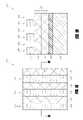
- FIG. 1Ashows a schematic top plan view of a masking stack on a substrate, including a first definable layer (e.g., photoresist) having a pattern of lines. Section hatching is employed in the plan views to illustrate correspondence with cross sections.
- a first definable layere.g., photoresist
- FIG. 1Bshows a schematic, cross-sectional side view taken along lines 1 B- 1 B of FIG. 1A .
- FIG. 2Ashows a schematic plan view of the structure of FIG. 1A after a selective etch has partially extended the first line pattern into an underlying first temporary layer (e.g., a sacrificial hard mask formed from transparent carbon).
- a first temporary layere.g., a sacrificial hard mask formed from transparent carbon.
- FIG. 2Bshows a schematic, cross-sectional side view taken along lines 2 B- 2 B of FIG. 2A .
- the A figure(e.g., FIG. 3A ) shows a schematic plan view of the surface.
- the B figure(e.g., FIG. 3B ) shows a schematic, cross-sectional side view taken along lines B-B (e.g., 3 B- 3 B) of the A figure (e.g., FIG. 3A ).
- the C figure(e.g., FIG. 3C ) shows a schematic, cross-sectional side view taken along lines C-C (e.g., 3 C- 3 C) of the A figure (e.g., FIG. 3A ).
- the D figure(e.g., FIG. 3D ) shows a schematic, cross-sectional side view taken along lines D-D (e.g., 3 D- 3 D) of the A figure (e.g., FIG. 3A ).
- FIGS. 3A-3Dshow the structure of FIGS. 2A-2D after removal of the first definable layer, deposition of a planarized filler material (e.g., BARC), and formation of a second line pattern of a second definable material (e.g., photoresist), where the second lines are formed cross-wise to the first pattern of lines.
- a planarized filler materiale.g., BARC
- a second line pattern of a second definable materiale.g., photoresist
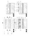
- FIGS. 4A-4Dshow the structure of FIGS. 3A-3D after extension of the second line pattern into the filler material (e.g., using a BARC etch).
- FIGS. 5A-5Dshow the structure of FIGS. 4A-4D after extension of the first line pattern into the lower portion of the temporary layer and extension of the second, crossing line pattern into the upper portion of the temporary layer (using a selective carbon etch, for example).
- FIGS. 6A-6Dshow the structure of FIGS. 5A-5D after removal of remaining portions of the second definable layer and the filler material.
- FIG. 6Eshows a perspective view of the structure of FIGS. 6A-6D .
- FIGS. 7A-7Dshow the structure of FIGS. 6A-6D after width reduction of the line structures of FIGS. 6A-6E (e.g., using an isotropic etch).
- FIGS. 8A-8Dshow the structure of FIGS. 7A-7D after blanket deposition and subsequent etching of a spacer material (e.g., using a directional etch).
- FIG. 8Eshows a perspective view of the structure of FIGS. 8A-8D .
- FIGS. 9A-9Dshow the structure of FIGS. 8A-8D after removal of remaining exposed portions of the first temporary layer and extension of the grid pattern in to a second temporary layer (e.g., DARC).
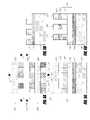
- a second temporary layere.g., DARC
- FIGS. 10A-10Dshow the structure of FIGS. 9A-9D after the remaining portions of the spacer material and remaining portions of the first temporary layer have been removed.
- FIGS. 11A-11Bshow the structure of FIGS. 10A-10B after the second temporary layer has been filled with a filler material (e.g., conductive material).
- a filler materiale.g., conductive material
- FIGS. 12A-12Bshow the structure of FIGS. 11A-11B after overflow filler material has been etched back to form isolated contacts in the substrate.
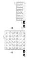
- FIG. 13is a scanning electron micrograph (SEM) illustrating a perspective view of a consolidated grid pattern formed according to the described embodiments.
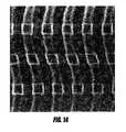
- FIG. 14is a scanning electron micrograph (SEM) illustrating a plan view of a consolidated grid pattern formed according to the described embodiments.
- a partially formed integrated circuit 100is provided.
- a substrate 150is provided below various masking layers 120 - 140 .
- the layers 120 - 140can be etched to form masks for patterning underlying layers or the substrate 150 .
- These maskscan be used to form various features, as discussed below.
- the featurescan comprise, for example, portions of any of the following: transistors, diodes, resistors, capacitors, conductive lines, gates, sources, drains, programmable fuse elements, programmable conductor RAM (PCRAM) elements, such as silver-doped chalcogenide glass, or contacts to any of the above.
- the featuresare formed from a substrate material that comprises a semi-conducting material.
- the semi-conducting materialcan be silicon, silicon-germanium compounds, or III-V materials.
- the preferred embodimentscan be used to form any integrated circuit, they are particularly advantageously applied to forming devices having arrays of electrical lines or devices, including memory cell arrays for volatile and non-volatile memory devices such as DRAM, phase change memory (PCM), programmable conductor RAM (PCRAM), ROM or flash memory, including NAND flash memory, or integrated circuits having logic or gate arrays.
- the logic arraycan be a field programmable gate array (FPGA) having a core array similar to a memory array and a periphery with supporting logics. Consequently, the integrated circuit 100 can be, e.g., a memory chip or a processor, which can include both a logic array and embedded memory, or any other integrated circuit having a logic or a gate array.
- FIG. 1AThe surfaces visible in FIG. 1A have been hatched for convenience to reveal the underlying materials of the structure depicted and to show which portions of the plan view correspond to structures depicted in cross-sectional views. Similar plan-view hatching is used throughout this description.
- the term “substrate”can refer not only to the substrate layer 150 , but also to the entire subassembly, including previously formed layers and the underlying substrate or workpiece (e.g., silicon wafer).
- substratecan also encompass a layer or layers that have features or structures formed within them as a result of a semiconductor process (e.g., etching, doping, depositing, etc.) controlled by overlying masking layers.
- the term “pattern”can refer to an array or series of shapes that would be visible on a surface if viewed from above.
- a patterncan refer to the ensemble of shapes that correspond to a cross-section or shadow of features formed in one or multiple layers. The pattern is generally not the features themselves, but rather the layout or design corresponding to the sizes and arrangement of the features.
- a patterncan be defined by a combination of patterns derived from multiple overlying or side-by-side layers.
- a patterncan originate in one layer, such as a photodefinable layer, and then be transferred to another layer, such as a temporary layer or a hard mask layer. The pattern is said to be transferred to lower layers even if feature sizes and spacings are altered (e.g., by a feature shrink step).
- a new patterncan be defined by pitch multiplication, whereby two or more features in the second pattern replace one feature of the first pattern.
- a pattern in one layercan be derived from one or more patterns in another previous or overlying layer.
- a patterncan be said to be derived from another pattern even if the features in the resulting layer do not exactly resemble those features which gave rise to the original pattern, but rather the underlying pattern generally follows the outline of the overlying pattern with minor deviations in dimensions.
- the term “to pattern”can also be used as a verb and means to create or form a pattern.
- An arrayis a collection of electrical components or features, formed in a repeating configuration, that can span multiple layers of an integrated circuit. As described above, multiple cells can form a memory array for a DRAM or NAND flash memory circuit, for example, or a logic array. An arrangement of features formed in a particular layer can have a corresponding pattern. An array can similarly have a corresponding pattern.
- the materials for the substrate 150 and the layers 120 - 140 overlying the substrate 150are preferably chosen based upon consideration of the chemistry and process conditions for the various pattern forming and pattern transferring steps discussed herein. Because the layers between a topmost selectively definable layer 120 —which preferably is definable by a lithographic process—and the substrate 150 will preferably function to transfer a pattern derived (at least in part) from the selectively definable layer 120 to the substrate 150 , the layers between the selectively definable layer 120 and the substrate 150 are preferably chosen so that they can be selectively etched relative to other exposed materials. A material is considered selectively, or preferentially, etched when the etch rate for that material is at least about five times greater, preferably about ten times greater and, most preferably, at least about forty times greater than that for surrounding materials.
- both the mask and the underlying substrateare exposed to an etchant, which preferentially etches away the substrate material.
- the etchantscan also wear away the mask materials, albeit at a slower rate.
- the maskcan be worn away by the etchant before the pattern transfer is complete.
- one or more of the layerscan be omitted in some embodiments.
- hard mask layersmay play a protective role, protecting underlying layers from unwanted degradation during etching of overlying layers.
- various other layersmay be omitted and overlying mask layers may be sufficient for the desired pattern transfer.
- Higher numbers of mask layersare advantageous for transferring patterns to difficult to etch substrates, such as a substrate comprising multiple materials or multiple layers of materials, or for forming small and high aspect ratio features.
- crossing striped patternsare formed, each having a pitch definable by photolithography, and consolidated into a grid pattern in a single layer.
- One example of a process sequence for this phaseis the following: 1) deposition of multiple layers; 2) photolithographic patterning of a first photosensitive layer; 3) extension of the first pattern into underlying layers; 4) blanket deposition of a filler material; 5) formation and photolithographic patterning of a second photosensitive layer; and 6) extension of the second pattern into the same underlying layers having the first pattern.
- Another example of a process sequence for the first phaseis the following: 1) deposition of multiple layers; 2) photolithographic patterning of a first photosensitive layer; 3) shrinking the features in the first pattern; 4) extension of the first pattern into underlying layers; 5) blanket deposition of a filler material; 6) formation and photolithographic patterning of a second photosensitive layer; 7) shrinking the features of the second pattern; and 8) extension of the second pattern into the same underlying layer(s) having the first pattern.
- FIGS. 6A-6Eshow how two patterns can operate together or be consolidated to effectively form a combined pattern or mask from two superimposed, crossing patterns. (Similarly, masks with different patterns at distinct layers can both shield the underlying layers or substrate).
- the term “level”is used to designate a portion of the integrated circuit that is generally located in a plane that is parallel to and equidistant from the plane of the surface of the substrate 150 .
- the term “layer”is generally used to refer to a portion of the integrated circuit formed from the same material and deposited in a single step.
- FIG. 1Ashows a schematic plan view of a first line pattern having lines 122 that have been patterned photolithographically in a first definable layer 120 .
- the first line patterncan be referred to as “vertical” or as “columns” herein because of the appearance of the lines 122 in the plan view of FIG. 1A .
- the same orientationis depicted consistently for FIGS. 1A , 2 A, 3 A, and so forth for all the figures labeled “A.” The same is true for the “B,” “C,” and “D” figures.
- FIG. 1Bshows a cross section through the structure of FIG. 1A .
- Underlying the first definable layer 120is a first temporary layer 130 with an upper portion 132 and a lower portion 134 .
- the upper portion 132is visible in FIG. 1A between the lines 122 formed in the first definable layer 120 .
- the first temporary layer 130serves as a sacrificial hard mask.
- the upper portion 132 and lower portion 134can be formed from different materials and form separate layers.
- Amorphous carbon and particularly transparent carbonis a preferred material for the first temporary layer 130 because so many other materials-silicon, silicon oxide, silicon nitride, etc.—can be selectively etched without significantly harming the carbon layer and because carbon is relatively resistant to high temperatures processing, compared to resists.
- a second temporary layer 140Underlying the lower portion 134 of the first temporary layer 130 is a second temporary layer 140 .
- the second temporary layer 140can be formed from a dielectric anti-reflective coating, or DARC.
- a substrate 150Underlying the second temporary layer 140 is a substrate 150 , which can be a silicon wafer, for example.
- the definable layer 120can be formed from photoresist.
- the photoresistcan be any photoresist compatible with 13.7 nanometer (nm), 157 nm, 193 nm, 248 nm or 365 nm wavelength systems, 193 nm wavelength immersion systems or electron beam lithographic systems.
- preferred photoresist materialsinclude argon fluoride (ArF) sensitive photoresist, e.g., photoresist suitable for use with an ArF light source, and krypton fluoride (KrF) sensitive photoresist, e.g., photoresist suitable for use with a KrF light source.
- ArFargon fluoride
- KrFkrypton fluoride
- ArF photoresistsare preferably used with photolithography systems utilizing relatively short wavelength light, e.g., 193 nm.
- KrF photoresistsare preferably used with longer wavelength photolithography systems, such as 248 nm systems.
- the definable layer 120 and any subsequent resist layerscan be formed of a resist that can be patterned by nano-imprint lithography, e.g., by using a mold or mechanical force to pattern the resist.
- Photoresistis typically patterned by being exposed to radiation through a reticle and then developed.
- radiatione.g., light
- the radiationactivates a photosensitive compound, e.g., a photo-induced acid generator (PAG), which decreases the solubility of the photoresist, e.g., by causing it to polymerize.
- PAGphoto-induced acid generator
- Preferred embodimentsmay be applied using any definable material, including positive or negative photoresist.
- Some preferred photoresist reticleshave a critical dimension of approximately 95 nm.
- the first temporary layer 130can be formed of amorphous carbon, which offers very high etch selectivity relative to the other preferred hard mask materials. More preferably, the amorphous carbon is a form of transparent carbon that is highly transparent to light and which offers further improvements for photo alignment by being transparent to wavelengths of light used for such alignment. Deposition techniques for forming a highly transparent carbon can be found in A. Helmbold, D. Meissner, Thin Solid Films, 283 (1996) 196-203, the entire disclosure of which is incorporated herein by reference and made part of this specification.
- the material for the second temporary layer 140preferably comprises an inorganic material, and exemplary materials include silicon dioxide (SiO 2 ), silicon, or a dielectric anti-reflective coating (DARC), such as a silicon-rich silicon oxynitride.
- the second temporary layer 140is a dielectric anti-reflective coating (DARC).
- DARCdielectric anti-reflective coating
- the second temporary layer 140can serve both as an intermediate hard mask and to reduce reflections during lithography.
- DARC material for the second temporary layer 140can be particularly advantageous for forming patterns having pitches near the resolution limits of a photolithographic technique.
- the DARCcan enhance resolution by minimizing light reflections, thus increasing the precision with which photolithography can define the edges of a pattern.
- the substrate 150can include a silicon wafer used for formation of integrated circuits with or without overlying materials. Various substrate materials can be used.
- the thicknesses of the layers 120 - 140are preferably chosen depending upon compatibility with the etch chemistries and process conditions described herein. For example, when transferring a pattern from an overlying layer to an underlying layer by selectively etching the underlying layer, materials from both layers are removed to some degree.
- the upper layeris preferably thick enough so that it is not worn away over the course of the pattern transfer. Thin hard mask layers can allow their transfer or removal to occur quickly, exposing surrounding materials to less wear.
- the selectively definable layer 120is a photodefinable layer preferably between about 100-500 nm thick and, more preferably, between about 150-280 nm thick.
- the first temporary layer 130e.g., amorphous carbon
- the second temporary layer 140is preferably between about 15-120 nm thick and, more preferably, between about 30-60 nm thick.
- various layers discussed hereincan be formed by various methods known to those of skill in the art.
- various vapor deposition processessuch as chemical vapor deposition
- a low temperature chemical vapor deposition processis used to deposit the hard mask layers or any other materials, e.g., spacer material, over carbon.
- Such low temperature deposition processesadvantageously prevent chemical or physical disruption of the underlying amorphous carbon layer.
- Spin-on-coating processescan be used to form photodefinable layers.
- amorphous carbon layerscan be formed by chemical vapor deposition using a hydrocarbon compound, or a mixture of such compounds, as a carbon precursor.
- Exemplary precursorsinclude propylene, propyne, propane, butane, butylene, butadiene and acetylene.
- a suitable method for forming amorphous carbon layersis described in U.S. Pat. No. 6,573,030 B1, issued to Fairbairn et al. on Jun. 3, 2003, the entire disclosure of which is incorporated herein by reference and made part of this specification.
- the amorphous carbonmay be doped.
- a suitable method for forming doped amorphous carbonis described in U.S. patent application Ser. No. 10/652,174 to Yin et al., the entire disclosure of which is incorporated herein by reference and made part of this specification.
- a pattern comprising gaps or spaces 123 delimited by the lines 122is formed in the definable layer 120 .
- the lines 122 and spaces 123can be formed by, e.g., photolithography, in which the selectively definable layer 120 is exposed to radiation through a reticle and then developed. After being developed, the remaining definable material, photoresist in the illustrated embodiment, forms mask features such as the illustrated lines 122 (shown in cross-section). In some embodiments, the widths of the features (e.g., lines 122 ) of the mask are in a range of approximately 50-200 nm.
- the pitch of the first line pattern of FIGS. 1A-1Bis equal to the sum of the width of a line 122 and the width of a neighboring space 123 .
- the pitchis preferably at or near the limits of the photolithographic technique used to pattern the definable layer 120 .
- the pitch of the lines 122can be about 200 nm.
- the pitchmay be at the minimum pitch of the photolithographic technique and the spacer pattern discussed below can advantageously have a pitch below the minimum pitch of the photolithographic technique.
- a preliminary stepcan comprise creating a series of photoresist lines 122 .
- photolithographycan be used to form a plurality of lines in a mask material.
- Conventional photolithographycan form lines having a pitch no smaller than that definable by photons.
- subsequent pitch multiplicationcan form lines having a pitch that is smaller than that definable by conventional photolithography.
- the features of a patternare prepared for pitch multiplication by a shrink step that reduces the widths of the protruding, positive features (such as lines or columns or blocks) and increases the widths of negative features (such as trenches or spaces or holes or voids).
- the shrink stepcan leave provide more room in between positive features for a spacer material to be deposited on and extend outwardly from the sidewalls of the positive features.
- the photoresist lines 122can undergo a shrink step after they are originally patterned.
- a shrink stepFor example, an isotropic etch can reduce the widths of the lines 122 and increase the widths of the spaces 123 .
- An SO 2 plasma-based vapor etchis an exemplary trim etch for photoresist. If a shrink step occurs at this stage before the first pattern is transferred into the first temporary layer 130 , a later shrink step (see FIGS. 7A-7D ) can be avoided or improved.
- FIGS. 2A-2Bshow the structure of FIGS. 1A-1B after a selective etch (e.g., a carbon etch) has extended or transferred the first line pattern into the underlying upper portion 132 of the first temporary layer 130 to form lines 222 .
- the first temporary layer 130is monolithic and the upper portion 132 is indistinguishable from the lower portion 134 before the selective etch.
- the selective etchdefines the relative thicknesses of the upper portion 132 and the lower portion 134 .
- the selective etchextends partially into (e.g., about halfway down into) the temporary layer 130 .
- FIG. 2Ashows a schematic plan view of the surface.
- FIG. 2Ashows a schematic plan view of the surface.
- FIG. 2Bshows a schematic, cross-sectional side view taken along lines 2 B- 2 B of FIG. 2A .
- This pattern extension or transfercan be accomplished by selectively etching the material that forms the first temporary layer 130 , while the lines 122 form a protective mask that prevents the etchant from removing the material located underneath the lines 122 .
- an additional layer(not shown) can be applied above the temporary layer 130 .
- the additional layercan be formed from DARC, for example, and can have sufficient thickness to have an upper portion and a lower portion, similar to the upper portion 132 and the lower portion 134 of the temporary layer 130 .
- the partial etch and other description herein relating to the temporary layer 130can apply to the overlying layer, and the structure and/or pattern thus created in the overlying layer can be transferred into the temporary layer 130 , which can be formed from carbon, for example.
- a patternis formed in an overlying layer and later transferred to an underlying layer.
- the illustrated walls of the features formed in layers 120 and 130are vertical, where these layers have been etched.
- directional or anisotropic etchescan be used.
- Variations in etching processescan alter the precision with which a pattern in an overlying layer corresponds to a pattern created in an underlying layer.
- pattern transfer from layer to layeris generally illustrated schematically to be a precise process, with features having vertical side walls, such precision may be difficult to achieve in practice.
- pattern transferis intended to encompass general correspondence between underlying and overlying patterns.
- pattern transferis meant to encompass modification of the features originally defining the pattern—for example by enlarging or shrinking those features—where such modification does not change the pitch.
- an SO 2 -containing plasmae.g., a plasma containing SO 2 , O 2 and Ar
- the SO 2 -containing plasmacan etch carbon of the preferred first temporary layer 130 at a rate greater than 20 times and, more preferably, greater than 40 times the rate that the definable layer 120 is etched.
- a suitable SO 2 -containing plasmais described in U.S. patent application Ser. No. 10/931,772 to Abatchev et al., filed Aug. 31, 2004, entitled Critical Dimension Control, (Atty. docket No. MICRON.286A; Micron Ref. No.
- FIGS. 2A-2Bshow lines 122 intact after the pattern has been extended into the first temporary layer 130 , the SO 2 -containing plasma can simultaneously etch the temporary layer 130 and also remove the remaining portion of definable layer 120 .
- FIGS. 3A-3Dshow the structure of FIGS. 2A-2B after any remaining portions of the first definable layer 120 are removed by a selective etch.
- One etch that can be usedhas a selectivity of approximately 8:1, and has the following low pressure recipe: O 2 flows at approximately 400 sccm, N 2 H 2 flows at approximately 400 sccm, CF 4 flows at approximately 40 sccm, the temperatures is approximately 150 degrees C., the pressure is approximately 150 mT, and the applied power is approximately 2000 W.
- a filler material 320(e.g., a bottom anti-reflective coating, or BARC material) has also been deposited between the lines 222 of the first temporary layer 132 to form alternating lines 322 of filler material 320 in between the lines 222 in the upper portion 132 of the first temporary layer 130 .
- the filler material 320has also been deposited over the top of the alternating stripes formed by the lines 222 and the lines 322 , but the borders between the hidden, underlying lines 222 and 322 are shown in phantom in FIG. 3A .
- the filler material 320(e.g., BARC) can be deposited using a spin-on process to provide for a smooth, self-planarizing layer.
- the filler material 320can be deposited by a more conformal process followed by planarization (e.g., a dry etch back or polishing process).
- a second selectively definable layer 330(formed, for example, from photoresist) has been deposited over the filler material 320 and patterned to form a second (horizontal or row) line pattern having lines 332 that are not parallel to the lines 122 of the first line pattern.
- the underlying first vertical line patternis perpendicular to the overlying second horizontal line pattern.
- the selectively defined lines 332can undergo a shrink step after they are originally patterned.
- an isotropic etchcan reduce the widths of the lines 332 and increase the widths of the spaces in between the lines 332 (e.g., SO 2 plasma based etch without bias).
- This shrink stepcan be substantially similar to the alternative described (but not illustrated) above with respect to the lines 122 .
- a later shrink stepsee FIGS. 7A-7D ) can be avoided and the resulting grid pattern can have good resolution and sharp corners where lines intersect.
- the holes and pillarscan have sidewalls that are more angular where sidewalls intersect, creating square rather than rounded holes and corners. (See FIGS. 6A-7E for schematic illustrations of holes and pillars).
- FIGS. 4A-4Dshow the structure of FIGS. 3A-3D after exposed portions of the filler layer 320 have been removed (using a selective BARC etch, for example).
- the lines 332 of the second definable layer 330form a protective mask that shields some portions (rows in the illustrated embodiment) of the filler material 320 such that the second line pattern has been extended into the filler material 320 .
- FIGS. 5A-5Dshow the structure of FIGS. 4A-4D after the exposed portions of the first temporary layer 130 have been partially removed (using a selective carbon etch, for the preferred temporary layer material), extending the first line pattern into the lower portion 134 of the first temporary layer 130 , and extending the second, crossing line pattern into the upper portion 132 of the temporary layer 130 .
- the extent of the etch that extends the second, crossing line pattern into the upper portion 132 of the temporary layer 130can be controlled or timed, allowing the etch to penetrate part-way (e.g., half-way) through the temporary layer 130 .
- both the temporary layer 130 and the filler material 320can be etched by the same etch process (e.g., if both layers contain carbon).
- FIGS. 6A-6Dshow the structure of FIGS. 5A-5D after any remaining portions of the second definable layer 330 and the remaining portions of the filler material 320 have been removed, leaving exposed a three-tiered structure.
- Thiscan be accomplished in the same etch process described above (e.g., carbon etch) if the definable layer 120 and the filler material 320 are both organic materials.
- a dry develop step or an SO 2 or O 2 -containing plasmacan be used.
- the lowest of the three exposed tierscomprises those parts of the second temporary layer 140 masked by neither the first (horizontal) nor the second (vertical) line patterns.
- the middle exposed tiercomprises exposed segments of the lower portion 134 of the first temporary layer 130 .
- the highest of the three exposed tierscomprises exposed segments of the upper portion 132 of the first temporary layer 130 .
- the highest of the three exposed tierscomprises the top surfaces of pillars 620 .
- FIG. 6Eshows a perspective view of the structure illustrated in FIGS. 6A-6D .
- the three-tiered structureis visible.
- the top (exposed) surface of the second temporary layer 140is the lower tier, representing twice-etched regions of the first temporary layer 130 .
- the generally square portions of the temporary layer 140 that are exposed in this figureare located in a generally vertical column of materials that has been subjected to multiple etch processes (two in the illustrated embodiment) without being protected by a mask. That is, the lower tier portions have not been protected from the carbon etches by either the first or second line patterns.
- the generally vertical column of materialshas been etched away through multiple etches until in the illustrated stage, nothing remains of that vertical column of materials above the exposed lower tier portions of the second temporary layer 140 .
- Top surfaces of the lower portion 134 of the temporary layer 130form the middle tier. As shown, what remains of the lower portion 134 of the temporary layer 130 forms a grid that overlies the second temporary layer 140 . Both the first (vertical or column) and second (horizontal or row) line patterns have been consolidated into the grid. The middle tier portions have been protected by one of the first and second line patterns, but not by both.
- the pillars 620have been protected from multiple etches because both the first and second (crossing) line patterns have protected the pillars 620 .
- FIGS. 6A-6Eschematically depict various features, including pillars 620 , a grid pattern, and holes in the grid pattern. These features are depicted as having relatively sharp corners; the pillars and grid holes have side walls that are generally flat, and intersect at right angels. In practice these corners may be somewhat more rounded due to the properties of the materials used, the chemistries employed to achieve the structure, etc. However, one way to provide for sharper corners on these features is to perform a shrink step on (reduce the width of) each of the first lines 122 and second lines 332 before those line patterns are transferred to underlying layers.
- the temporary layer 130may have another temporary layer (not shown) above it.
- the other temporary layercan have the two-tier structure depicted in FIGS. 6A-6E , and the two-tier structure can then be transferred into the temporary layer 130 .
- the two-tier structure created in the overlying layercan be created in the same way described here for the temporary layer 130 .
- the overlying temporary layercan be formed from DARC, and the temporary layer 130 can be formed from carbon.
- the two temporary layerscan both be relatively thick so that each can have an upper portion and a lower portion created through a half-etch or partial-etch process, as illustrated for the temporary layer 130 .
- a grid patternis pitch reduced and transferred to underlying layers.
- One example of an etch sequence for this phaseis the following: 1) shrink feature (mandrel) widths (to the extent not already shrunk); 2) blanket deposition of spacer material; 3) spacer etch; 4) removal of mandrels; and 5) extension of spacer pattern into underlying material.
- Another example of an etch sequence for this phaseis to skip step 1 because the feature widths have been reduced already in the first phase.
- FIGS. 7A-7Dshow the structure of FIGS. 6A-6D after an etch (e.g., an isotropic carbon etch) has reduced the widths of the remaining portions of the first temporary layer 130 .
- the width of the grid lines formed in the lower portion 134has been reduced.
- the width of the pillars 620 formed in the upper portion 132has been reduced, forming narrow pillars 720 .
- the masking lines in both the first (vertical) and second (horizontal) line patternshave been shrunk or reduced so that the spaces in between lines are wider and the lines' widths are diminished, but the pitch of neither the first (vertical) nor the second (horizontal) line pattern has changed.
- the grid lines and pillars 620are preferably reduced in size using an isotropic carbon etch, such as an etch containing SO 2 and O 2 plasma without bias.
- the extent of the etchis preferably selected so that the widths of the modified grid lines and narrow pillars 720 are substantially equal to the desired spacing between the later-formed spacers 820 , as will be appreciated from the discussion of FIGS. 8-9 .
- this etchallows the modified grid lines and narrow pillars 720 to be narrower than would otherwise be possible using the photolithographic technique used to pattern the photodefinable layers 120 and 330 . That is, if the lines 122 ( FIGS. 1A-2B ) and the lines 332 ( FIGS.
- this etchcan reduce their size even further, taking them below that resolution limit.
- the etchcan smooth the edges of the modified grid lines and narrow pillars 720 , thus improving their uniformity.
- the spaces between the grid lines and pillars 620can be narrowed by expanding the grid lines and pillars 620 to a desired size.
- additional material(not shown) can be deposited over the grid lines, or the grid lines can be chemically reacted to form a material (not shown) having a larger volume to increase their size.
- the modified grid lines and narrow pillars 720define the dimensions of placeholders or mandrels along which a pattern of spacers will be formed after blanket deposition of a spacer material 820 ( FIGS. 8A-9D ).
- the grid patterncan be first transferred to the second temporary layer 140 and the spacer material can be deposited directly on the second temporary layer 140 .
- the first temporary layer 130is preferably formed of a material that can withstand the process conditions for spacer material deposition and etch, discussed below.
- the material forming the temporary layer 130preferably has a higher heat resistance than photoresist and is preferably selected such that it can be selectively removed relative to the material for the spacers 820 ( FIG. 8 ) and the underlying second temporary layer 140 .
- the first temporary layer 130is preferably formed of transparent carbon.
- FIGS. 8A-8Eshow the structure of FIGS. 7A-7D after deposition and subsequent etching of a spacer material 820 .
- the spacer material 820(formed from an oxide material, for example) has first been blanket deposited over the narrow grid lines and narrow pillars 720 of FIG. 7 .
- the depositionis to a thickness of the desired spacer width, conformally deposited over the mandrels.
- the spacer material 820has then been anisotropically etched (using a reactive ion etch, for example) to create a grid of spacers—the spacers adhering to the side walls of the narrow grid lines and the narrow pillars 720 . Formation of these spacers has formed a pattern that is pitch multiplied in two dimensions when compared to the pitch of the grid pattern of FIGS. 6 and 7 .
- FIG. 8Eshows a perspective view of the general structure of the contours of spacer material 820 adhered to the side walls of the temporary layer 130 .
- the spacer material 820adheres to the sides of the columns 720 , which are located at the intersections of the rows and columns formed in the lower portion 134 of the temporary layer 130 . In this way, lines of spacer material 820 can bridge over each row or column and form a continuous hard-mask grid.
- FIG. 8Fshows a section taken through one of the continuous lines of spacer material 820 , showing how the spacer material bridging over successive lines in the lower portion 134 of the temporary layer 130 .
- a layer of spacer material 820is preferably blanket deposited so that it conforms to the exposed surfaces, including the walls of the narrow grid lines and the narrow pillars 720 .
- the spacer materialcan be any material that can act as a mask for transferring a pattern to underlying layers, or that otherwise can allow processing of underlying structures through the mask being formed.
- the spacer materialpreferably: 1) can be deposited with good step coverage; 2) can be deposited at a temperature compatible with the first temporary layer 130 and underlying layers; and 3) can be selectively etched relative to the first temporary layer 130 and any layer directly underlying the first temporary layer 130 .
- Preferred materialsinclude silicon, silicon oxides, and nitrides.
- High aspect ratio process (HARP) oxidescan also be used.
- HARP oxidescan be deposited at relatively low temperatures with high conformality.
- the spacer materialis preferably deposited by chemical vapor deposition or atomic layer deposition to a thickness corresponding to the desired width of the mask features, which in the illustrated embodiment is between about 20-60 nm and, more preferably, about 20-50 nm.
- the step coverageis about 80% or greater and, more preferably, about 90% or greater.
- the spacer etchcan comprise an anisotropic etch to remove spacer material from horizontal surfaces.
- the spacer etchcan be performed using a fluorocarbon plasma (e.g., CF 4 /CHF 3 , C 4 F 8 /CH 2 F 2 or CHF 3 /Ar). Fluorocarbon plasmas such as these can be used with an amorphous silicon hard mask, carbon mandrels, and silicon oxide spacers, for example.
- the spacer etchcan also be performed using HBr/Cl plasma for a silicon spacer material.
- some embodimentshave feature patterns with lines that have been reduced in width before the patterns are transferred to underlying layers.
- photoresist linescan undergo a direct shrink step.
- Such an approachcan provide for well-defined corners in a grid pattern and provide for features (e.g., square holes and square pillars) with flat surfaces. These surfaces can provide large surface areas. This good coverage can, in turn, allow for improved functionality in a final product. For example, a capacitor configured in a hole with flat sides and sharper corners can have a higher capacitance than a hole with more rounded corners.
- FIGS. 9A-9Dshow the structure of FIGS. 8A-8E after remaining exposed portions of the first temporary layer have been removed (using a selective carbon etch, for example), leaving a pitch-multiplied, masking grid pattern formed by spacer material.
- the grid patternhas been extended into the underlying second temporary layer 140 with a selective etch (e.g., a DARC etch) that does not attack the oxide of the spacers 820 (formed from HARP oxide, for example), thus creating holes that expose isolated portions of the underlying substrate layer 150 (which can be formed from silicon or silicon oxide, for example). In this way, features of one pattern are removed to leave behind another pattern formed by the spacers.
- a selective etche.g., a DARC etch
- pitch-reductionhas been performed using a spacer material to create masking features.
- the masking features formed in this waycan have a smaller pitch than the photoresist lines and can comprise pitch-reduced masking lines separated by pitch-reduced spaces; pitch multiplication has been accomplished.
- the pitch of the pattern formed by spacersis roughly half that of the pattern corresponding to definable lines 122 and 332 ( FIGS. 1A-5D ), where the pitch was originally determined by photolithography.
- a spacer pattern having a pitch of about 50-150 nmcan be formed (e.g., 100 nm pitch where original lithography defined a 200 nm pitch).
- a spacer etchAs illustrated, after a spacer etch is performed, it can leave behind a grid pattern of spacer material 820 having effectively reduced pitch relative to the grid pattern of spacer mandrels (the lines and pillars of the temporary layer 130 ).
- a mask patternformed from spacer material 820 .
- the mask patterncomprises a pitch-multiplied grid of spacer material 820 having pairs of crossing lines forming intersections. The pairs of crossing lines are the spacer lines that had adhered to each column or row of the grid and each pillar 720 . When the columns and rows of the grid are removed, the spacer line pairs remain.
- the spacer line pairsintersect where the pillars 720 had been at the intersections of the grid rows and columns. However, after removal of the pillars 720 as well as the directly underlying mandrel grid at the intersection upon which the pillars 720 had stood, the spacer line pairs form the tall side-walls of deep holes 920 and shallow holes 930 .
- the depth of the deep holes 920correspond to the height of the pillars 720 that have been removed. Holes of a similar depth are also formed in between the two members of each spacer line pair, in between the portions of spacer material 820 that had adhered to adjacent pillars 720 prior to removal of the temporary layer 130 .
- the line pairs of spacer materialalso form the side walls of shallower holes at other regions of the array.
- the depth of the shallow holes 930correspond to the height of the lines in the grid of spacer material, exposed portions of which have been removed.
- the lines of spacer materialform side-walls of shallow holes 930 where the underlying second temporary layer 140 was already exposed, even before removal of remaining exposed portions of the temporary layer 130 .
- These shallow holes 930are formed between separate pairs of spacer lines. Holes 930 of a similar depth are also formed in between the two members of each spacer line pair, where the row mandrel or column mandrel was located prior to removal of the temporary layer 130 .
- FIGS. 10A-10Dshow the structure of FIGS. 9A-9D after the remaining portions of the spacer material 820 and remaining portions of the first temporary layer 130 (up until now protected under the spacers 820 ) have been removed with one or multiple selective etches, leaving behind a pitch-multiplied mask grid formed from the second temporary layer 140 .
- the mask gridhas regularly-spaced holes 1012 that reveal isolated portions of the underlying substrate 150 .
- FIG. 10Ashows a schematic plan view of the surface. After this etch step, the second temporary layer 140 exhibits features that were present in two distinct overlying patterns: the first (vertical or column) line pattern and the second (horizontal or row) line pattern.
- One or multiple etch stepscan be used to remove the remaining portions of the overlying layers to achieve the structure illustrated in FIGS. 10A-10D .
- a single etch stepcan remove all of the overlying layers at once with a CMP process, a sputter etch, a dry etch, a reactive ion etch, or any chemistry or process that removes everything but the materials of the layers 140 and 150 .
- the spacer material 820 and the remaining portions of the layer 130have been completely removed in FIGS. 10A-10D , leaving a masking grid sitting atop the layer 150 .
- the masking gridhas small holes 1012 that can occur at regular intervals in two dimensions (see FIG. 10A ).
- the holes 1012have a slightly rectangular footprint.
- the footprints of the featuresare square—that is, the length and width of the features are approximately the same in overhead plan view.
- the featureshave a first width of less than approximately 50 nanometers and a first length of approximately 1.5 times the first width, for a width to length ratio of approximately 1:1.5. More generally, the width to length ratio is preferably between about 1:1 and 1:2.
- preferred embodimentsform features that are isolated, rather than continuous lines. Pitch multiplication of a pattern in one dimension can result in pitch multiplied lines, but pitch multiplication of crossing patterns can result in small, dense, isolated features.
- Pitch multiplication of crossing patternscan be particularly advantageous when the pitch multiplication occurs in a consolidated step after the crossing patterns have already been consolidated or combined in two levels (upper and lower portions 132 and 134 ) of a single layer ( 130 ), for example.
- the features having a length that is not many times longer than the feature's widthare thus different from lines, which may have a length thousands of times their width, for example.
- Preferred embodimentshave features with a less-elongate footprint, instead having a more square-shaped footprint.
- the featurespreferably are spaced apart at intervals of less than approximately 50 nm.
- the isolated featureseach have a rectangular footprint with dimensions of approximately 50 nm by approximately 75 nm.
- the isolated featureseach have a square footprint with dimensions of approximately 50 nm by approximately 50 nm.
- the processes and method described aboveprovide the advantage of a single shrink step and/or a single spacer process to produce a pitch-multiplied pattern in two dimensions.
- a single shrink step and/or a single spacer processto produce a pitch-multiplied pattern in two dimensions.
- two or more distinct line patternscan be shrunk in a single etch
- spacer materialcan be deposited on mandrels for the various patterns in a single deposition step
- the mandrels for the various patternscan be removed in a single etch.
- fewer stepscan be used to accomplish isolated features that have been pitch multiplied in two dimensions.
- the grid of mask materialin the illustrated embodiment the patterned second temporary layer 140 ) is used to create features in or on the substrate 150 .
- the hard mask 140can be omitted and the spacer patterns of FIG. 8 (after removal of the mandrels) can be used directly as the mask.
- FIGS. 11A-11Bshow the structure of FIGS. 10A-10B after the pattern of holes 1012 in the second temporary layer 140 has been extended into the substrate 150 , the second temporary layer 140 has been removed, and the corresponding holes in the substrate have been filled with a conductive material 1120 .
- the substrate 150comprises an upper insulating layer and the openings in the substrate expose lower circuit elements to which contact is desired (e.g., source/drain regions of transistors).
- the conductive material 1120preferably substantially fills the holes 1012 in the substrate 150 and overflows to form a continuous overflow layer, as illustrated.
- the conductive material 1120can be any electrically conducting or semi-conducting material. In a preferred embodiment, the conductive material 1120 is doped polysilicon.
- the conductive material 1120can be a conductive metal such as tungsten, copper, or aluminum.
- the conductive material 1120often includes multiple sublayers. For example, a titanium adhesion layer, a metal nitride barrier layer, and a metal filler layer can all be used in combination.
- FIGS. 12A-12Bshow the structure of FIGS. 11A-11B after the overflow conductive material has been etched back to the surface of the substrate 150 .
- the overflow materialis removed using a CMP process.
- a hard mask layer(not shown) can be deposited between the second temporary layer 140 and the substrate 150 to act as a CMP stop.
- Some embodimentscan use a reactive ion etch (RIE) or a sputter etch to remove the overflow material.
- RIEreactive ion etch
- portions of the conductive material 1120form isolated contacts that are densely and/or regularly spaced.
- Preferred contactshave a pitch width of less than 150 nm. More preferably, such contacts have a pitch width of approximately 100 nm or less.
- the holes 1012can be used to pattern or form other isolated features, such as conductive posts for stud capacitors, trenches for trench capacitors, and/or selective epitaxial posts for transistors.
- the mask holescan be used to pattern features formed from a semiconductor. These features can be formed by selective epitaxy in the mask holes, which can expose portions of a single-crystal silicon layer below the mask layer.
- the featurescan comprise vertical surround gate transistors that connect a source region (not shown) in an underlying level to a drain that is part of the isolated semiconductor pillar grown through the mask holes 1012 .
- the holecan have within it, or the feature can act as, a channel connecting a source region to a drain.
- the contactsare formed in the extension of the holes 1012 into the substrate 150 , as described above.
- the dimensions of each contactare advantageously determined by the resolution of a spacer pattern formed using the spacer material 820 .
- the contactshave a symmetrical, square footprint.
- the contactsare shaped to correspond to the features they are designed to contact.
- circuit elementscan be formed by filling the mask grid itself with material.
- the modified layer 140(the grid with holes that overlies the substrate 150 ) can be filled directly with conductive material instead of extending the holes 1012 into the underlying substrate layer 110 .
- the overflow conductive materialcan be removed and the second temporary layer 140 can be removed to leave freestanding conductive contacts on the substrate 150 .
- the spaces between contactscan then be filled with an insulating material such as oxide (not shown).
- the pattern of modified layer 140is first extended into the upper portion of the substrate 150 (such as an ILD), and contacts are formed at the lower level.
- the holes 1012are configured to receive an electrically conductive material such as metal. Furthermore, when used in formation of an integrated circuit, the holes 1012 are preferably positioned to allow formation of an electrically conductive contact that connects underlying features such as transistor source regions with other components (for example, bit lines) in an overlying level.
- the contactscan have different configurations.
- the featuresmay have corners that are less sharply-defined than those of the illustrated contacts in FIG. 12B .
- the proportions, shape, spacing, height, width, and contours of the contactsmay vary from the illustration in FIG. 12B .
- the contactsare polysilicon plugs.
- the contactsconnect elements of memory arrays; however, such contacts can connect portions of any electrical device or component to any other electrical device or component.
- the skilled artisanwill readily appreciate other applications for employing the mask with a dense pattern of holes.
- An alternative way to form a grid structure that can be used for making contactsis to fill the holes 1012 with a cap material (not shown) that can be selective etched with respect to the second temporary layer 140 , polish back any overflow cap material, selectively remove grid formed by the second temporary layer 140 , leaving islands of the cap material in place.
- This inverse mask patterncan then be used, for example, to form pillars of the substrate 150 by etching away the portions of the substrate 150 that are not protected by the islands of cap material.
- These pillarscan, in turn be used to create a grid if the space between the pillars is filled with another material and the pillars are removed.
- pillars or posts and gridscan be formed in adjacent portions of an array.
- pillars or postscan be formed from a semiconducting material.
- carbon islandscan be used as a mask to etch silicon pillars in an underlying semiconducting substrate.
- the second temporary layer 140can be omitted and the holes 1012 can be formed directly in the substrate 150 , which can be a silicon wafer or a blanket epitaxial layer.
- the holes 1012can be extended into or formed directly in the substrate 150 .
- the resulting holes in the substrate 150can thus be the features formed by methods described above.
- the resulting holes in the substrate 150can be lined with a dielectric material and can function as portions of capacitors, for example.
- the holes 1012 or corresponding holes in the substrate 150can be filled with phase change materials, which change conductivity with switchable changes in phase, in a process to form phase change memories; programmable conductor memories (PCRAM); or filled with fusable materials (e.g., positively or negatively doped polysilicon or metals) in a process to form programmable read only memories (PROMs); etc.
- Phase change memoriesare memories having a material which can be switched between relatively conductive and insulating states by the application of heat.
- Exemplary phase change materialsinclude germanium, antimony and tellurium alloys (also referred to as GeSbT or GST).
- PCRAMProgrammable conductor RAM
- a programmable conductore.g., chalcogenide glass doped with silver or other high mobility metal
- the conductorscan cause shorts in the glass when an electric field is applied in one direction and can dissolve back into an amorphous glass phase when an opposite electric field is applied.
- Fusable materialse.g., aluminum and polysilicon in PROMs can be used as fuses, which are retained or “blown” as desired to establish a desired conductive state in the memory.
- electrical devices and/or parts thereof, such as capacitorsmay be formed using the voids 310 .
- FIGS. 13 and 14are scanning electron micrographs (SEMs) illustrating a dense array of small holes formed according to the described embodiments. These SEMs show structure that can be used to make holes having a pitch of approximately 200 nm by 250 nm. The features shown have a width of approximately 95 nm in the critical dimension.
- FIGS. 1-6the process described in FIGS. 1-6 was generally followed, with the exception that an extra layer of DARC was used above the temporary layer 130 .
- the extra DARC layerwas approximately 1200 angstroms ( ⁇ ) thick.
- the half-etch process resulting in multiple exposed layerswas accomplished in the DARC layer and then transferred into the underlying temporary layer 130 (which was formed from transparent carbon (TC) in this example).
- TCtransparent carbon
- FIG. 13the DARC layer has been removed after the pattern was extended into the TC layer.
- the TCis approximately 3,000 ⁇ thick and overlies an oxide layer.
- the underlying oxide layer in this exampleis approximately 20,000 ⁇ thick and is PSG oxide.
- the first pattern(generally corresponding to the lines 122 in FIG. 1 above) was a serpentine (wavy line) pattern with a pitch of approximately 195 nm.
- the next crossing pattern(generally corresponding to the lines 332 of FIG. 3 ) had a pitch of approximately 293 nm.
- holes resulting from these two patternscan be approximately 98 nm by approximately 147 nm.
- the pitch doubling processcan thus produce features of approximately 50 nm by 75 nm with the structure shown here.
- Pillarshave been formed where the two line patterns cross. These pillars correspond to the narrow pillars 720 schematically illustrated above (see FIG. 7 ).
- the SEM of FIG. 13has features that do not line up directly, but are offset in a regular wavy pattern. Because of this wavy pattern, the grid pattern may not be precisely square or rectangular as illustrated schematically in the figures above. As this figure illustrates, there are many embodiments and configurations covered by the inventions disclosed herein.
- FIG. 14is an SEM illustrating a dense array of small holes formed according to the described embodiments.
- FIG. 14shows a plan view wherein the features have a pitch of approximately 200 nm by 250 nm.
Landscapes
- Engineering & Computer Science (AREA)
- Manufacturing & Machinery (AREA)
- Physics & Mathematics (AREA)
- Condensed Matter Physics & Semiconductors (AREA)
- General Physics & Mathematics (AREA)
- Computer Hardware Design (AREA)
- Microelectronics & Electronic Packaging (AREA)
- Power Engineering (AREA)
- Chemical & Material Sciences (AREA)
- Inorganic Chemistry (AREA)
- Semiconductor Memories (AREA)
- Internal Circuitry In Semiconductor Integrated Circuit Devices (AREA)
Abstract
Description
- This application is a divisional of U.S. patent application Ser. No. 11/217,270, filed Sep. 1, 2005.
- This application is related to the following: U.S. patent application Ser. No. 11/215,982 (MICRON.313A) filed Aug. 31, 2005; U.S. patent application Ser. No. 11/134,982 (MICRON.317A) filed May 23, 2005; and U.S. patent application Ser. No. 11/219,346 (MICRON.330A) filed Sep. 1, 2005. Each of the above-mentioned references is hereby incorporated by reference in its entirety and made part of this specification.
- 1. Field of the Inventions
- The disclosed invention relates generally to integrated circuit fabrication, techniques for fabrication of computer memory, and masking techniques.
- 2. Description of the Related Art
- As a consequence of many factors, including demand for increased portability, computing power, memory capacity and energy efficiency in modern electronics, integrated circuits are continuously being reduced in size. To facilitate this size reduction, research continues into ways of reducing the sizes of integrated circuits' constituent features. Examples of those constituent features include capacitors, electrical contacts, interconnecting lines, and other electrical devices. The trend of decreasing feature size is evident, for example, in memory circuits or devices such as dynamic random access memories (DRAMs), static random access memories (SRAMs), ferroelectric (FE) memories, electronically-erasable programmable read-only memories (EEPROMs), flash memories, etc.
- Computer memory typically comprises millions of identical circuit elements, known as memory cells, arranged in a plurality of arrays with associated logic circuitry. Each memory cell traditionally stores one bit of information, although multi-level cell devices can store more than one bit per cell. A conventional DRAM memory cell typically consists of two electrical devices: a storage capacitor and an access field effect transistor. Each memory cell is an addressable location that can store one bit (binary digit) of data. A bit can be written to a cell through the transistor and read by sensing charge on the storage electrode from the reference electrode side. One common type of computer memory that can benefit from higher density components is DRAM. By decreasing the sizes of constituent electrical devices, the conducting lines that connect them, and the conductive contacts carrying charge between them, the sizes of the memory devices incorporating these features can be decreased. Note that some memory arrangements can combine the storage and switch functions in a single device (e.g., dendritic memories using silver-doped chalcogenide glass elements) and others can omit the access device (e.g., magnetic RAM). Storage capacities and circuit speed can be increased by fitting more memory cells into the memory devices.
- The concept of pitch can be used to describe the size of integrated circuit features. Pitch is the distance between identical points in two neighboring features. These features are typically defined by spaces between adjacent features, which spaces may be filled by a material, such as an insulator. As a result, pitch can be viewed as the sum of the width of a feature and of the width of the space separating that feature from a neighboring feature. When the pitch is reduced, features are more dense—that is, more features can fit onto the same surface. Although it may seem counterintuitive, the term “pitch reduction” is synonymous with “pitch multiplication” in common usage. That is, conventionally “multiplication” of pitch by a certain factor actually involves reducing the pitch by that factor. The term “pitch multiplication” emphasizes that more features can fit in the same area, while the term “pitch reduction” emphasizes that in order for more features to fit, those features are generally smaller. Pitch thus has at least two meanings: the linear spacing between identical features in a repeating pattern; and the density or number of features per linear distance. The conventional terminology is retained herein.
- The demand for continual reduction in feature sizes places ever greater demands on techniques used to form the features. For example, photolithography is commonly used to pattern features on a substrate. Certain photoresist materials only respond to certain wavelengths of light. One common range of wavelengths that can be used lies in the ultraviolet (UV) range. Because many photoresist materials respond selectively to particular wavelengths, photolithography techniques each have a minimum pitch below which that particular photolithographic technique cannot reliably form features. This minimum pitch is often determined by the wavelength of light that can be used with that technique. Thus, the minimum pitch of a photolithographic technique can limit feature size reduction.
- Pitch multiplication can extend the capabilities of photolithographic techniques to allow creation of more densely arranged features. Such a method is described in U.S. Pat. No. 5,328,810, issued to Lowrey et al., the entire disclosure of which is incorporated herein by reference and made part of this specification.
- The critical dimension (CD) of a mask scheme or circuit design is the scheme's minimum feature dimension, or the measurement of the smallest width of the smallest feature that exists in that design or scheme. Due to factors such as geometric complexity and different requirements for critical dimensions in different parts of an integrated circuit, typically not all features of the integrated circuit will be pitch multiplied. Furthermore, pitch multiplication entails many additional steps relative to conventional lithography; the additional steps can involve considerable additional expense. Pitch multiplication often provides less control over the resulting features than that provided by direct patterning without pitch multiplication. Thus, pitch multiplication is typically thought useful for regularly spaced lines, such as conductive lines for a memory array. On the other hand, typical micromasking techniques, such as isotropic shrink steps, can result in a reduction in feature size but no corresponding increase in feature density. There have also been challenges in transferring very fine patterns to underlying layers because existing techniques do not adequately maintain resolution and fidelity through the transfer. There is a need for methods that can allow for smaller and more efficient operative units on an integrated circuit; such methods will advantageously increase feature density and decrease chip size.
- Thus, there is a need for a reduction in the size of integrated circuits and an increased operable density of the arrays of electrical devices on computer chips.
- Some embodiments provide a method of forming features in an array. For example, a first masking grid of crossing lines can be provided, the first masking grid corresponding to a first grid pattern. Furthermore, the pitch of the crossing lines of the masking grid can be simultaneously reduced to form a second masking grid of spacer lines, and the second masking grid can correspond to a second grid pattern.
- Some embodiments provide a method of forming a feature array for an integrated circuit. For example, a first feature array can be formed in a first mask layer, a plurality of first features of the first feature array being elongate with a first axis of elongation. The first feature array can have a first pattern. A second feature array can be formed in a second mask layer, a plurality of second features of the second feature array having elongate features with a second axis of elongation that is not parallel to the first axis. The second feature array can have a second pattern. The first and second patterns can be consolidated into a combined third pattern, the third pattern corresponding to an arrangement of features in two vertical levels of the integrated circuit. Moreover, spacers can be simultaneously formed on sidewalls of both the first features and the second features.
- Some embodiments provide a method of forming isolated features in an integrated circuit. For example, a substrate can be provided that is overlaid by multiple layers of masking material. A first series of selectively definable lines can be created in a first layer of masking material, the first series of lines corresponding to a first pattern. A second series of selectively definable lines can be created in a second layer of masking material, the second series of lines not parallel to the first series of selectively definable lines, the second series of lines corresponding to a second pattern. The pitch of both the first series and the second series of selectively definable lines can be concurrently reduced using a spacer material to create a grid of masking features having a smaller pitch than either the first or second series of selectively definable lines, the grid corresponding to a third pattern derived by superimposing the first and second patterns. The third pattern into the substrate can also be extended to form isolated features.
- Some embodiments provide a method of forming features in an array. For example, a first masking grid of rows that cross columns can be provided, the first masking grid corresponding to a first grid pattern. A second masking grid of spacer lines can be formed by forming spacers or sidewalls of both the rows and columns, the second masking grid corresponding to a second grid pattern. A second grid pattern can be transferred to an underlying masking layer.
- Some embodiments provide an array of features for computer memory fabrication. The array can have a middle tier comprising a grid with crossing lines, holes, and intersections, the lines having side walls. The array can also have a lower tier comprising a surface upon which the grid is positioned, the lower tier being exposed in the holes between the crossing grid lines. The array can also have a higher tier comprising pillars positioned on the grid where the grid lines cross at the intersections, the pillars having side walls.
- Some embodiments have a hard mask comprising a non pitch-multiplied grid of masking material having crossing lines forming intersections and holes between intersections. The hard mask can also have pillars of masking material positioned on the grid at the intersections.
- Some embodiments have a mask comprising a pitch-multiplied grid of masking material having pairs of crossing lines forming intersections. The mask can also have deep holes formed between line pairs where line pairs bridge over underlying structure and shallow holes formed between crossing line pairs where the line pairs do not bridge over any underlying structure.
- Some embodiments provide a method of forming a hard mask. For example, a temporary layer can be provided and partially etched the temporary layer with a first pattern. The temporary layer can also be partially etched with a second pattern.
- The inventions will be further understood from the Detailed Description of the Preferred Embodiments and from the appended drawings, which illustrate and do not limit the inventions. The Figures show various masking, temporary, and substrate layers used in an integrated circuit. In particular:
FIG. 1A shows a schematic top plan view of a masking stack on a substrate, including a first definable layer (e.g., photoresist) having a pattern of lines. Section hatching is employed in the plan views to illustrate correspondence with cross sections.FIG. 1B shows a schematic, cross-sectional side view taken alonglines 1B-1B ofFIG. 1A .FIG. 2A shows a schematic plan view of the structure ofFIG. 1A after a selective etch has partially extended the first line pattern into an underlying first temporary layer (e.g., a sacrificial hard mask formed from transparent carbon).FIG. 2B shows a schematic, cross-sectional side view taken alonglines 2B-2B ofFIG. 2A .- In
FIGS. 3-10 , the A figure (e.g.,FIG. 3A ) shows a schematic plan view of the surface. The B figure (e.g.,FIG. 3B ) shows a schematic, cross-sectional side view taken along lines B-B (e.g.,3B-3B) of the A figure (e.g.,FIG. 3A ). The C figure (e.g.,FIG. 3C ) shows a schematic, cross-sectional side view taken along lines C-C (e.g.,3C-3C) of the A figure (e.g.,FIG. 3A ). The D figure (e.g.,FIG. 3D ) shows a schematic, cross-sectional side view taken along lines D-D (e.g.,3D-3D) of the A figure (e.g.,FIG. 3A ). FIGS. 3A-3D show the structure ofFIGS. 2A-2D after removal of the first definable layer, deposition of a planarized filler material (e.g., BARC), and formation of a second line pattern of a second definable material (e.g., photoresist), where the second lines are formed cross-wise to the first pattern of lines.FIGS. 4A-4D show the structure ofFIGS. 3A-3D after extension of the second line pattern into the filler material (e.g., using a BARC etch).FIGS. 5A-5D show the structure ofFIGS. 4A-4D after extension of the first line pattern into the lower portion of the temporary layer and extension of the second, crossing line pattern into the upper portion of the temporary layer (using a selective carbon etch, for example).FIGS. 6A-6D show the structure ofFIGS. 5A-5D after removal of remaining portions of the second definable layer and the filler material.FIG. 6E shows a perspective view of the structure ofFIGS. 6A-6D .FIGS. 7A-7D show the structure ofFIGS. 6A-6D after width reduction of the line structures ofFIGS. 6A-6E (e.g., using an isotropic etch).FIGS. 8A-8D show the structure ofFIGS. 7A-7D after blanket deposition and subsequent etching of a spacer material (e.g., using a directional etch).FIG. 8E shows a perspective view of the structure ofFIGS. 8A-8D .FIGS. 9A-9D show the structure ofFIGS. 8A-8D after removal of remaining exposed portions of the first temporary layer and extension of the grid pattern in to a second temporary layer (e.g., DARC).FIGS. 10A-10D show the structure ofFIGS. 9A-9D after the remaining portions of the spacer material and remaining portions of the first temporary layer have been removed.FIGS. 11A-11B show the structure ofFIGS. 10A-10B after the second temporary layer has been filled with a filler material (e.g., conductive material).FIGS. 12A-12B show the structure ofFIGS. 11A-11B after overflow filler material has been etched back to form isolated contacts in the substrate.FIG. 13 is a scanning electron micrograph (SEM) illustrating a perspective view of a consolidated grid pattern formed according to the described embodiments.FIG. 14 is a scanning electron micrograph (SEM) illustrating a plan view of a consolidated grid pattern formed according to the described embodiments.- With reference to
FIGS. 1A-1B , a partially formedintegrated circuit 100 is provided. Asubstrate 150 is provided below various masking layers120-140. The layers120-140 can be etched to form masks for patterning underlying layers or thesubstrate 150. These masks can be used to form various features, as discussed below. The features can comprise, for example, portions of any of the following: transistors, diodes, resistors, capacitors, conductive lines, gates, sources, drains, programmable fuse elements, programmable conductor RAM (PCRAM) elements, such as silver-doped chalcogenide glass, or contacts to any of the above. In some embodiments, the features are formed from a substrate material that comprises a semi-conducting material. For example, the semi-conducting material can be silicon, silicon-germanium compounds, or III-V materials. - While the preferred embodiments can be used to form any integrated circuit, they are particularly advantageously applied to forming devices having arrays of electrical lines or devices, including memory cell arrays for volatile and non-volatile memory devices such as DRAM, phase change memory (PCM), programmable conductor RAM (PCRAM), ROM or flash memory, including NAND flash memory, or integrated circuits having logic or gate arrays. For example, the logic array can be a field programmable gate array (FPGA) having a core array similar to a memory array and a periphery with supporting logics. Consequently, the
integrated circuit 100 can be, e.g., a memory chip or a processor, which can include both a logic array and embedded memory, or any other integrated circuit having a logic or a gate array. - The surfaces visible in
FIG. 1A have been hatched for convenience to reveal the underlying materials of the structure depicted and to show which portions of the plan view correspond to structures depicted in cross-sectional views. Similar plan-view hatching is used throughout this description. - As used in this specification, the term “substrate” can refer not only to the
substrate layer 150, but also to the entire subassembly, including previously formed layers and the underlying substrate or workpiece (e.g., silicon wafer). The term “substrate” can also encompass a layer or layers that have features or structures formed within them as a result of a semiconductor process (e.g., etching, doping, depositing, etc.) controlled by overlying masking layers. - As used in this specification, the term “pattern” can refer to an array or series of shapes that would be visible on a surface if viewed from above. A pattern can refer to the ensemble of shapes that correspond to a cross-section or shadow of features formed in one or multiple layers. The pattern is generally not the features themselves, but rather the layout or design corresponding to the sizes and arrangement of the features. A pattern can be defined by a combination of patterns derived from multiple overlying or side-by-side layers. A pattern can originate in one layer, such as a photodefinable layer, and then be transferred to another layer, such as a temporary layer or a hard mask layer. The pattern is said to be transferred to lower layers even if feature sizes and spacings are altered (e.g., by a feature shrink step). In contrast, a new pattern can be defined by pitch multiplication, whereby two or more features in the second pattern replace one feature of the first pattern.
- A pattern in one layer can be derived from one or more patterns in another previous or overlying layer. A pattern can be said to be derived from another pattern even if the features in the resulting layer do not exactly resemble those features which gave rise to the original pattern, but rather the underlying pattern generally follows the outline of the overlying pattern with minor deviations in dimensions. The term “to pattern” can also be used as a verb and means to create or form a pattern.
- An array is a collection of electrical components or features, formed in a repeating configuration, that can span multiple layers of an integrated circuit. As described above, multiple cells can form a memory array for a DRAM or NAND flash memory circuit, for example, or a logic array. An arrangement of features formed in a particular layer can have a corresponding pattern. An array can similarly have a corresponding pattern.
- The materials for the
substrate 150 and the layers120-140 overlying thesubstrate 150 are preferably chosen based upon consideration of the chemistry and process conditions for the various pattern forming and pattern transferring steps discussed herein. Because the layers between a topmost selectivelydefinable layer 120—which preferably is definable by a lithographic process—and thesubstrate 150 will preferably function to transfer a pattern derived (at least in part) from the selectivelydefinable layer 120 to thesubstrate 150, the layers between the selectivelydefinable layer 120 and thesubstrate 150 are preferably chosen so that they can be selectively etched relative to other exposed materials. A material is considered selectively, or preferentially, etched when the etch rate for that material is at least about five times greater, preferably about ten times greater and, most preferably, at least about forty times greater than that for surrounding materials. - In common methods of transferring patterns, both the mask and the underlying substrate are exposed to an etchant, which preferentially etches away the substrate material. The etchants, however, can also wear away the mask materials, albeit at a slower rate. Thus, over the course of transferring a pattern, the mask can be worn away by the etchant before the pattern transfer is complete. These difficulties are exacerbated where the
substrate 150 comprises multiple different materials to be etched. In such cases, additional mask layers may be used to prevent the mask pattern from being worn away before the pattern transfer is complete. - Because the various layers are chosen based upon the requirements of chemistry and process conditions, one or more of the layers can be omitted in some embodiments. In some embodiments, hard mask layers may play a protective role, protecting underlying layers from unwanted degradation during etching of overlying layers. Similarly, for a particularly simple substrate, various other layers may be omitted and overlying mask layers may be sufficient for the desired pattern transfer. Higher numbers of mask layers are advantageous for transferring patterns to difficult to etch substrates, such as a substrate comprising multiple materials or multiple layers of materials, or for forming small and high aspect ratio features.
- In a first phase of methods in accordance with the preferred embodiments and with reference to
FIGS. 1A-6E , crossing striped patterns are formed, each having a pitch definable by photolithography, and consolidated into a grid pattern in a single layer. One example of a process sequence for this phase is the following: 1) deposition of multiple layers; 2) photolithographic patterning of a first photosensitive layer; 3) extension of the first pattern into underlying layers; 4) blanket deposition of a filler material; 5) formation and photolithographic patterning of a second photosensitive layer; and 6) extension of the second pattern into the same underlying layers having the first pattern. - Another example of a process sequence for the first phase is the following: 1) deposition of multiple layers; 2) photolithographic patterning of a first photosensitive layer; 3) shrinking the features in the first pattern; 4) extension of the first pattern into underlying layers; 5) blanket deposition of a filler material; 6) formation and photolithographic patterning of a second photosensitive layer; 7) shrinking the features of the second pattern; and 8) extension of the second pattern into the same underlying layer(s) having the first pattern.
- As discussed herein, masks with different patterns at distinct levels can both shield the underlying layers or substrate.
FIGS. 6A-6E , for example, show how two patterns can operate together or be consolidated to effectively form a combined pattern or mask from two superimposed, crossing patterns. (Similarly, masks with different patterns at distinct layers can both shield the underlying layers or substrate). - For convenience in this application, the term “level” is used to designate a portion of the integrated circuit that is generally located in a plane that is parallel to and equidistant from the plane of the surface of the
substrate 150. In contrast, the term “layer” is generally used to refer to a portion of the integrated circuit formed from the same material and deposited in a single step. FIG. 1A shows a schematic plan view of a first linepattern having lines 122 that have been patterned photolithographically in a firstdefinable layer 120. The first line pattern can be referred to as “vertical” or as “columns” herein because of the appearance of thelines 122 in the plan view ofFIG. 1A . In the figures, the same orientation is depicted consistently forFIGS. 1A ,2A,3A, and so forth for all the figures labeled “A.” The same is true for the “B,” “C,” and “D” figures.FIG. 1B shows a cross section through the structure ofFIG. 1A . Underlying the firstdefinable layer 120 is a firsttemporary layer 130 with anupper portion 132 and alower portion 134. Theupper portion 132 is visible inFIG. 1A between thelines 122 formed in the firstdefinable layer 120. The firsttemporary layer 130 serves as a sacrificial hard mask. In some embodiments, theupper portion 132 andlower portion 134 can be formed from different materials and form separate layers. Amorphous carbon and particularly transparent carbon is a preferred material for the firsttemporary layer 130 because so many other materials-silicon, silicon oxide, silicon nitride, etc.—can be selectively etched without significantly harming the carbon layer and because carbon is relatively resistant to high temperatures processing, compared to resists. Underlying thelower portion 134 of the firsttemporary layer 130 is a secondtemporary layer 140. The secondtemporary layer 140 can be formed from a dielectric anti-reflective coating, or DARC. Underlying the secondtemporary layer 140 is asubstrate 150, which can be a silicon wafer, for example.- The
definable layer 120 can be formed from photoresist. For example, the photoresist can be any photoresist compatible with 13.7 nanometer (nm), 157 nm, 193 nm, 248 nm or 365 nm wavelength systems, 193 nm wavelength immersion systems or electron beam lithographic systems. Examples of preferred photoresist materials include argon fluoride (ArF) sensitive photoresist, e.g., photoresist suitable for use with an ArF light source, and krypton fluoride (KrF) sensitive photoresist, e.g., photoresist suitable for use with a KrF light source. ArF photoresists are preferably used with photolithography systems utilizing relatively short wavelength light, e.g., 193 nm. KrF photoresists are preferably used with longer wavelength photolithography systems, such as 248 nm systems. In other embodiments, thedefinable layer 120 and any subsequent resist layers can be formed of a resist that can be patterned by nano-imprint lithography, e.g., by using a mold or mechanical force to pattern the resist. - Photoresist is typically patterned by being exposed to radiation through a reticle and then developed. In the case of negative photoresist, radiation, e.g., light, is focused on parts of the photoresist that are to be retained, e.g., on the areas where the lines—such as lines124 (see FIG.3)—are to be formed. Typically, the radiation activates a photosensitive compound, e.g., a photo-induced acid generator (PAG), which decreases the solubility of the photoresist, e.g., by causing it to polymerize. Preferred embodiments may be applied using any definable material, including positive or negative photoresist. Some preferred photoresist reticles have a critical dimension of approximately 95 nm.
- The first
temporary layer 130 can be formed of amorphous carbon, which offers very high etch selectivity relative to the other preferred hard mask materials. More preferably, the amorphous carbon is a form of transparent carbon that is highly transparent to light and which offers further improvements for photo alignment by being transparent to wavelengths of light used for such alignment. Deposition techniques for forming a highly transparent carbon can be found in A. Helmbold, D. Meissner,Thin Solid Films,283 (1996) 196-203, the entire disclosure of which is incorporated herein by reference and made part of this specification. - The material for the second
temporary layer 140 preferably comprises an inorganic material, and exemplary materials include silicon dioxide (SiO2), silicon, or a dielectric anti-reflective coating (DARC), such as a silicon-rich silicon oxynitride. In the illustrated embodiment, the secondtemporary layer 140 is a dielectric anti-reflective coating (DARC). Thus, the secondtemporary layer 140 can serve both as an intermediate hard mask and to reduce reflections during lithography. Using DARC material for the secondtemporary layer 140 can be particularly advantageous for forming patterns having pitches near the resolution limits of a photolithographic technique. The DARC can enhance resolution by minimizing light reflections, thus increasing the precision with which photolithography can define the edges of a pattern. - The
substrate 150 can include a silicon wafer used for formation of integrated circuits with or without overlying materials. Various substrate materials can be used. - In addition to selecting appropriate materials for the various layers, the thicknesses of the layers120-140 are preferably chosen depending upon compatibility with the etch chemistries and process conditions described herein. For example, when transferring a pattern from an overlying layer to an underlying layer by selectively etching the underlying layer, materials from both layers are removed to some degree. Thus, in some embodiments, the upper layer is preferably thick enough so that it is not worn away over the course of the pattern transfer. Thin hard mask layers can allow their transfer or removal to occur quickly, exposing surrounding materials to less wear.
- In the illustrated embodiment, the selectively definable layer120 (e.g., photoresist) is a photodefinable layer preferably between about 100-500 nm thick and, more preferably, between about 150-280 nm thick. The first temporary layer130 (e.g., amorphous carbon) is preferably between about 100-500 nm thick and, more preferably, between about 150-300 nm thick. The second temporary layer140 (e.g., DARC) is preferably between about 15-120 nm thick and, more preferably, between about 30-60 nm thick.
- The various layers discussed herein can be formed by various methods known to those of skill in the art. For example, various vapor deposition processes, such as chemical vapor deposition, can be used to form the various hard mask layers under the resist. Preferably, a low temperature chemical vapor deposition process is used to deposit the hard mask layers or any other materials, e.g., spacer material, over carbon. Such low temperature deposition processes advantageously prevent chemical or physical disruption of the underlying amorphous carbon layer. Spin-on-coating processes can be used to form photodefinable layers. In addition, amorphous carbon layers can be formed by chemical vapor deposition using a hydrocarbon compound, or a mixture of such compounds, as a carbon precursor. Exemplary precursors include propylene, propyne, propane, butane, butylene, butadiene and acetylene. A suitable method for forming amorphous carbon layers is described in U.S. Pat. No. 6,573,030 B1, issued to Fairbairn et al. on Jun. 3, 2003, the entire disclosure of which is incorporated herein by reference and made part of this specification. In addition, the amorphous carbon may be doped. A suitable method for forming doped amorphous carbon is described in U.S. patent application Ser. No. 10/652,174 to Yin et al., the entire disclosure of which is incorporated herein by reference and made part of this specification.
- With further reference to
FIG. 1B , a pattern comprising gaps orspaces 123 delimited by thelines 122 is formed in thedefinable layer 120. Thelines 122 andspaces 123 can be formed by, e.g., photolithography, in which the selectivelydefinable layer 120 is exposed to radiation through a reticle and then developed. After being developed, the remaining definable material, photoresist in the illustrated embodiment, forms mask features such as the illustrated lines122 (shown in cross-section). In some embodiments, the widths of the features (e.g., lines122) of the mask are in a range of approximately 50-200 nm. - The pitch of the first line pattern of
FIGS. 1A-1B is equal to the sum of the width of aline 122 and the width of a neighboringspace 123. To minimize the critical dimensions of features formed using this pattern oflines 122 andspaces 123, the pitch is preferably at or near the limits of the photolithographic technique used to pattern thedefinable layer 120. For example, for photolithography utilizing 248 nm light, the pitch of thelines 122 can be about 200 nm. Thus, the pitch may be at the minimum pitch of the photolithographic technique and the spacer pattern discussed below can advantageously have a pitch below the minimum pitch of the photolithographic technique. - As illustrated by
FIGS. 1A-1B , a preliminary step can comprise creating a series of photoresist lines122. Thus, photolithography can be used to form a plurality of lines in a mask material. Conventional photolithography can form lines having a pitch no smaller than that definable by photons. However, subsequent pitch multiplication can form lines having a pitch that is smaller than that definable by conventional photolithography. Often the features of a pattern are prepared for pitch multiplication by a shrink step that reduces the widths of the protruding, positive features (such as lines or columns or blocks) and increases the widths of negative features (such as trenches or spaces or holes or voids). The shrink step can leave provide more room in between positive features for a spacer material to be deposited on and extend outwardly from the sidewalls of the positive features. - Although not illustrated in
FIGS. 1A and 1B , thephotoresist lines 122 can undergo a shrink step after they are originally patterned. For example, an isotropic etch can reduce the widths of thelines 122 and increase the widths of thespaces 123. An SO2plasma-based vapor etch is an exemplary trim etch for photoresist. If a shrink step occurs at this stage before the first pattern is transferred into the firsttemporary layer 130, a later shrink step (seeFIGS. 7A-7D ) can be avoided or improved. FIGS. 2A-2B show the structure ofFIGS. 1A-1B after a selective etch (e.g., a carbon etch) has extended or transferred the first line pattern into the underlyingupper portion 132 of the firsttemporary layer 130 to formlines 222. In some embodiments, the firsttemporary layer 130 is monolithic and theupper portion 132 is indistinguishable from thelower portion 134 before the selective etch. Thus, the selective etch defines the relative thicknesses of theupper portion 132 and thelower portion 134. In some embodiments, the selective etch extends partially into (e.g., about halfway down into) thetemporary layer 130.FIG. 2A shows a schematic plan view of the surface.FIG. 2B shows a schematic, cross-sectional side view taken alonglines 2B-2B ofFIG. 2A . This pattern extension or transfer can be accomplished by selectively etching the material that forms the firsttemporary layer 130, while thelines 122 form a protective mask that prevents the etchant from removing the material located underneath thelines 122.- In some embodiments, an additional layer (not shown) can be applied above the
temporary layer 130. The additional layer can be formed from DARC, for example, and can have sufficient thickness to have an upper portion and a lower portion, similar to theupper portion 132 and thelower portion 134 of thetemporary layer 130. In this case, the partial etch and other description herein relating to thetemporary layer 130 can apply to the overlying layer, and the structure and/or pattern thus created in the overlying layer can be transferred into thetemporary layer 130, which can be formed from carbon, for example. - In the illustrated embodiment, a pattern is formed in an overlying layer and later transferred to an underlying layer. In
FIG. 2B , the illustrated walls of the features formed inlayers - Variations in etching processes can alter the precision with which a pattern in an overlying layer corresponds to a pattern created in an underlying layer. Although pattern transfer from layer to layer is generally illustrated schematically to be a precise process, with features having vertical side walls, such precision may be difficult to achieve in practice. Thus, pattern transfer is intended to encompass general correspondence between underlying and overlying patterns. Similarly, pattern transfer is meant to encompass modification of the features originally defining the pattern—for example by enlarging or shrinking those features—where such modification does not change the pitch.
- To transfer the first line pattern into the
upper portion 132 of the firsttemporary layer 130, an SO2-containing plasma, e.g., a plasma containing SO2, O2and Ar, is preferably used. Advantageously, the SO2-containing plasma can etch carbon of the preferred firsttemporary layer 130 at a rate greater than 20 times and, more preferably, greater than 40 times the rate that thedefinable layer 120 is etched. A suitable SO2-containing plasma is described in U.S. patent application Ser. No. 10/931,772 to Abatchev et al., filed Aug. 31, 2004, entitled Critical Dimension Control, (Atty. docket No. MICRON.286A; Micron Ref. No. 2003-1348), the entire disclosure of which is incorporated herein by reference and made part of this specification. AlthoughFIGS. 2A- 2B show lines 122 intact after the pattern has been extended into the firsttemporary layer 130, the SO2-containing plasma can simultaneously etch thetemporary layer 130 and also remove the remaining portion ofdefinable layer 120. FIGS. 3A-3D show the structure ofFIGS. 2A-2B after any remaining portions of the firstdefinable layer 120 are removed by a selective etch. One etch that can be used has a selectivity of approximately 8:1, and has the following low pressure recipe: O2flows at approximately 400 sccm, N2H2flows at approximately 400 sccm, CF4flows at approximately 40 sccm, the temperatures is approximately 150 degrees C., the pressure is approximately 150 mT, and the applied power is approximately 2000 W.- A filler material320 (e.g., a bottom anti-reflective coating, or BARC material) has also been deposited between the
lines 222 of the firsttemporary layer 132 to form alternatinglines 322 offiller material 320 in between thelines 222 in theupper portion 132 of the firsttemporary layer 130. Thefiller material 320 has also been deposited over the top of the alternating stripes formed by thelines 222 and thelines 322, but the borders between the hidden,underlying lines FIG. 3A . The filler material320 (e.g., BARC) can be deposited using a spin-on process to provide for a smooth, self-planarizing layer. Alternatively, thefiller material 320 can be deposited by a more conformal process followed by planarization (e.g., a dry etch back or polishing process). A second selectively definable layer330 (formed, for example, from photoresist) has been deposited over thefiller material 320 and patterned to form a second (horizontal or row) linepattern having lines 332 that are not parallel to thelines 122 of the first line pattern. InFIG. 3A , the underlying first vertical line pattern is perpendicular to the overlying second horizontal line pattern. - Although not illustrated in
FIGS. 3A-3D , the selectively definedlines 332 can undergo a shrink step after they are originally patterned. For example, an isotropic etch can reduce the widths of thelines 332 and increase the widths of the spaces in between the lines332 (e.g., SO2plasma based etch without bias). This shrink step can be substantially similar to the alternative described (but not illustrated) above with respect to thelines 122. If thefirst lines 122 and thesecond lines 332 are both shrunk (or reduced in width) before each respective line pattern is transferred to underlying layers, a later shrink step (seeFIGS. 7A-7D ) can be avoided and the resulting grid pattern can have good resolution and sharp corners where lines intersect. For example, the holes and pillars can have sidewalls that are more angular where sidewalls intersect, creating square rather than rounded holes and corners. (SeeFIGS. 6A-7E for schematic illustrations of holes and pillars). FIGS. 4A-4D show the structure ofFIGS. 3A-3D after exposed portions of thefiller layer 320 have been removed (using a selective BARC etch, for example). Thelines 332 of the seconddefinable layer 330 form a protective mask that shields some portions (rows in the illustrated embodiment) of thefiller material 320 such that the second line pattern has been extended into thefiller material 320.FIGS. 5A-5D show the structure ofFIGS. 4A-4D after the exposed portions of the firsttemporary layer 130 have been partially removed (using a selective carbon etch, for the preferred temporary layer material), extending the first line pattern into thelower portion 134 of the firsttemporary layer 130, and extending the second, crossing line pattern into theupper portion 132 of thetemporary layer 130. Preferably, the extent of the etch that extends the second, crossing line pattern into theupper portion 132 of thetemporary layer 130 can be controlled or timed, allowing the etch to penetrate part-way (e.g., half-way) through thetemporary layer 130. An underlying second temporary layer140 (formed from a dielectric anti-reflective coating, or DARC, for example) has been partially exposed in the areas unmasked by either the first or second line patterns. In some embodiments, both thetemporary layer 130 and thefiller material 320 can be etched by the same etch process (e.g., if both layers contain carbon).FIGS. 6A-6D show the structure ofFIGS. 5A-5D after any remaining portions of the seconddefinable layer 330 and the remaining portions of thefiller material 320 have been removed, leaving exposed a three-tiered structure. This can be accomplished in the same etch process described above (e.g., carbon etch) if thedefinable layer 120 and thefiller material 320 are both organic materials. For example, a dry develop step or an SO2or O2-containing plasma can be used. The lowest of the three exposed tiers comprises those parts of the secondtemporary layer 140 masked by neither the first (horizontal) nor the second (vertical) line patterns. The middle exposed tier comprises exposed segments of thelower portion 134 of the firsttemporary layer 130. The highest of the three exposed tiers comprises exposed segments of theupper portion 132 of the firsttemporary layer 130. The highest of the three exposed tiers comprises the top surfaces ofpillars 620.FIG. 6E shows a perspective view of the structure illustrated inFIGS. 6A-6D . The three-tiered structure is visible. The top (exposed) surface of the secondtemporary layer 140 is the lower tier, representing twice-etched regions of the firsttemporary layer 130. The generally square portions of thetemporary layer 140 that are exposed in this figure are located in a generally vertical column of materials that has been subjected to multiple etch processes (two in the illustrated embodiment) without being protected by a mask. That is, the lower tier portions have not been protected from the carbon etches by either the first or second line patterns. Thus, the generally vertical column of materials has been etched away through multiple etches until in the illustrated stage, nothing remains of that vertical column of materials above the exposed lower tier portions of the secondtemporary layer 140.- Top surfaces of the
lower portion 134 of thetemporary layer 130 form the middle tier. As shown, what remains of thelower portion 134 of thetemporary layer 130 forms a grid that overlies the secondtemporary layer 140. Both the first (vertical or column) and second (horizontal or row) line patterns have been consolidated into the grid. The middle tier portions have been protected by one of the first and second line patterns, but not by both. - The top surfaces of the
upper portion 132 of thetemporary layer 132, the tops of thepillars 620, form the higher tier. What remains of theupper portion 132 of the firsttemporary layer 130forms pillars 620 positioned on top of the grid at the intersection of the vertical and horizontal grid lines. Thepillars 620 have been protected from multiple etches because both the first and second (crossing) line patterns have protected thepillars 620. FIGS. 6A-6E schematically depict various features, includingpillars 620, a grid pattern, and holes in the grid pattern. These features are depicted as having relatively sharp corners; the pillars and grid holes have side walls that are generally flat, and intersect at right angels. In practice these corners may be somewhat more rounded due to the properties of the materials used, the chemistries employed to achieve the structure, etc. However, one way to provide for sharper corners on these features is to perform a shrink step on (reduce the width of) each of thefirst lines 122 andsecond lines 332 before those line patterns are transferred to underlying layers.- As described above, the
temporary layer 130 may have another temporary layer (not shown) above it. The other temporary layer can have the two-tier structure depicted inFIGS. 6A-6E , and the two-tier structure can then be transferred into thetemporary layer 130. The two-tier structure created in the overlying layer can be created in the same way described here for thetemporary layer 130. For example, the overlying temporary layer can be formed from DARC, and thetemporary layer 130 can be formed from carbon. The two temporary layers can both be relatively thick so that each can have an upper portion and a lower portion created through a half-etch or partial-etch process, as illustrated for thetemporary layer 130. - In a second phase of methods in accordance with the preferred embodiments and with reference to
FIGS. 7A-10D , a grid pattern is pitch reduced and transferred to underlying layers. One example of an etch sequence for this phase is the following: 1) shrink feature (mandrel) widths (to the extent not already shrunk); 2) blanket deposition of spacer material; 3) spacer etch; 4) removal of mandrels; and 5) extension of spacer pattern into underlying material. Another example of an etch sequence for this phase is to skipstep 1 because the feature widths have been reduced already in the first phase. FIGS. 7A-7D show the structure ofFIGS. 6A-6D after an etch (e.g., an isotropic carbon etch) has reduced the widths of the remaining portions of the firsttemporary layer 130. The width of the grid lines formed in thelower portion 134 has been reduced. Furthermore, the width of thepillars 620 formed in theupper portion 132 has been reduced, formingnarrow pillars 720. Thus, the masking lines in both the first (vertical) and second (horizontal) line patterns have been shrunk or reduced so that the spaces in between lines are wider and the lines' widths are diminished, but the pitch of neither the first (vertical) nor the second (horizontal) line pattern has changed.- The grid lines and
pillars 620 are preferably reduced in size using an isotropic carbon etch, such as an etch containing SO2and O2plasma without bias. The extent of the etch is preferably selected so that the widths of the modified grid lines andnarrow pillars 720 are substantially equal to the desired spacing between the later-formedspacers 820, as will be appreciated from the discussion ofFIGS. 8-9 . Advantageously, this etch allows the modified grid lines andnarrow pillars 720 to be narrower than would otherwise be possible using the photolithographic technique used to pattern the photodefinable layers120 and330. That is, if the lines122 (FIGS. 1A-2B ) and the lines332 (FIGS. 3A-5D ) and other underlying lines derived from these lines are at or near the resolution limit of the photolithographic technique, this etch can reduce their size even further, taking them below that resolution limit. In addition, the etch can smooth the edges of the modified grid lines andnarrow pillars 720, thus improving their uniformity. - In some embodiments, the spaces between the grid lines and
pillars 620 can be narrowed by expanding the grid lines andpillars 620 to a desired size. For example, additional material (not shown) can be deposited over the grid lines, or the grid lines can be chemically reacted to form a material (not shown) having a larger volume to increase their size. - In the illustrated embodiment, the modified grid lines and
narrow pillars 720 define the dimensions of placeholders or mandrels along which a pattern of spacers will be formed after blanket deposition of a spacer material820 (FIGS. 8A-9D ). In alternative embodiments, if the deposition and etch of spacer material is incompatible with thetemporary layer 130, the grid pattern can be first transferred to the secondtemporary layer 140 and the spacer material can be deposited directly on the secondtemporary layer 140. - The first
temporary layer 130 is preferably formed of a material that can withstand the process conditions for spacer material deposition and etch, discussed below. In particular, the material forming thetemporary layer 130 preferably has a higher heat resistance than photoresist and is preferably selected such that it can be selectively removed relative to the material for the spacers820 (FIG. 8 ) and the underlying secondtemporary layer 140. As noted above, the firsttemporary layer 130 is preferably formed of transparent carbon. - As described above, the width reduction of the features can happen in an earlier stage of the process. In this case, the width reduction (or shrink step) illustrated here may be skipped. For example, the widths may already be reduced relative to the spaces in between the crossing lines, leaving larger openings between features.
FIGS. 8A-8E show the structure ofFIGS. 7A-7D after deposition and subsequent etching of aspacer material 820. The spacer material820 (formed from an oxide material, for example) has first been blanket deposited over the narrow grid lines andnarrow pillars 720 ofFIG. 7 . Preferably, the deposition is to a thickness of the desired spacer width, conformally deposited over the mandrels. Thespacer material 820 has then been anisotropically etched (using a reactive ion etch, for example) to create a grid of spacers—the spacers adhering to the side walls of the narrow grid lines and thenarrow pillars 720. Formation of these spacers has formed a pattern that is pitch multiplied in two dimensions when compared to the pitch of the grid pattern ofFIGS. 6 and 7 . FIG. 8E shows a perspective view of the general structure of the contours ofspacer material 820 adhered to the side walls of thetemporary layer 130. Thespacer material 820 adheres to the sides of thecolumns 720, which are located at the intersections of the rows and columns formed in thelower portion 134 of thetemporary layer 130. In this way, lines ofspacer material 820 can bridge over each row or column and form a continuous hard-mask grid.FIG. 8F shows a section taken through one of the continuous lines ofspacer material 820, showing how the spacer material bridging over successive lines in thelower portion 134 of thetemporary layer 130.- As shown in
FIGS. 8A-8F , a layer ofspacer material 820 is preferably blanket deposited so that it conforms to the exposed surfaces, including the walls of the narrow grid lines and thenarrow pillars 720. The spacer material can be any material that can act as a mask for transferring a pattern to underlying layers, or that otherwise can allow processing of underlying structures through the mask being formed. The spacer material preferably: 1) can be deposited with good step coverage; 2) can be deposited at a temperature compatible with the firsttemporary layer 130 and underlying layers; and 3) can be selectively etched relative to the firsttemporary layer 130 and any layer directly underlying the firsttemporary layer 130. Preferred materials include silicon, silicon oxides, and nitrides. High aspect ratio process (HARP) oxides can also be used. HARP oxides can be deposited at relatively low temperatures with high conformality. The spacer material is preferably deposited by chemical vapor deposition or atomic layer deposition to a thickness corresponding to the desired width of the mask features, which in the illustrated embodiment is between about 20-60 nm and, more preferably, about 20-50 nm. Preferably, the step coverage is about 80% or greater and, more preferably, about 90% or greater. The spacer etch can comprise an anisotropic etch to remove spacer material from horizontal surfaces. The spacer etch can be performed using a fluorocarbon plasma (e.g., CF4/CHF3, C4F8/CH2F2or CHF3/Ar). Fluorocarbon plasmas such as these can be used with an amorphous silicon hard mask, carbon mandrels, and silicon oxide spacers, for example. The spacer etch can also be performed using HBr/Cl plasma for a silicon spacer material. - As described above, some embodiments have feature patterns with lines that have been reduced in width before the patterns are transferred to underlying layers. Thus, photoresist lines can undergo a direct shrink step. Such an approach can provide for well-defined corners in a grid pattern and provide for features (e.g., square holes and square pillars) with flat surfaces. These surfaces can provide large surface areas. This good coverage can, in turn, allow for improved functionality in a final product. For example, a capacitor configured in a hole with flat sides and sharper corners can have a higher capacitance than a hole with more rounded corners.
FIGS. 9A-9D show the structure ofFIGS. 8A-8E after remaining exposed portions of the first temporary layer have been removed (using a selective carbon etch, for example), leaving a pitch-multiplied, masking grid pattern formed by spacer material. The grid pattern has been extended into the underlying secondtemporary layer 140 with a selective etch (e.g., a DARC etch) that does not attack the oxide of the spacers820 (formed from HARP oxide, for example), thus creating holes that expose isolated portions of the underlying substrate layer150 (which can be formed from silicon or silicon oxide, for example). In this way, features of one pattern are removed to leave behind another pattern formed by the spacers.- Thus, in some embodiments, pitch-reduction has been performed using a spacer material to create masking features. The masking features formed in this way can have a smaller pitch than the photoresist lines and can comprise pitch-reduced masking lines separated by pitch-reduced spaces; pitch multiplication has been accomplished. In the illustrated embodiment, the pitch of the pattern formed by spacers is roughly half that of the pattern corresponding to
definable lines 122 and332 (FIGS. 1A-5D ), where the pitch was originally determined by photolithography. Preferably, a spacer pattern having a pitch of about 50-150 nm can be formed (e.g., 100 nm pitch where original lithography defined a 200 nm pitch). - As illustrated, after a spacer etch is performed, it can leave behind a grid pattern of
spacer material 820 having effectively reduced pitch relative to the grid pattern of spacer mandrels (the lines and pillars of the temporary layer130). After thepillars 720 and the remaining exposed portions of thetemporary layer 130 have been removed, what remains is a mask pattern formed fromspacer material 820. The mask pattern comprises a pitch-multiplied grid ofspacer material 820 having pairs of crossing lines forming intersections. The pairs of crossing lines are the spacer lines that had adhered to each column or row of the grid and eachpillar 720. When the columns and rows of the grid are removed, the spacer line pairs remain. The spacer line pairs intersect where thepillars 720 had been at the intersections of the grid rows and columns. However, after removal of thepillars 720 as well as the directly underlying mandrel grid at the intersection upon which thepillars 720 had stood, the spacer line pairs form the tall side-walls ofdeep holes 920 andshallow holes 930. The depth of thedeep holes 920 correspond to the height of thepillars 720 that have been removed. Holes of a similar depth are also formed in between the two members of each spacer line pair, in between the portions ofspacer material 820 that had adhered toadjacent pillars 720 prior to removal of thetemporary layer 130. - The line pairs of spacer material also form the side walls of shallower holes at other regions of the array. The depth of the
shallow holes 930 correspond to the height of the lines in the grid of spacer material, exposed portions of which have been removed. For example, the lines of spacer material form side-walls ofshallow holes 930 where the underlying secondtemporary layer 140 was already exposed, even before removal of remaining exposed portions of thetemporary layer 130. Theseshallow holes 930 are formed between separate pairs of spacer lines.Holes 930 of a similar depth are also formed in between the two members of each spacer line pair, where the row mandrel or column mandrel was located prior to removal of thetemporary layer 130. FIGS. 10A-10D show the structure ofFIGS. 9A-9D after the remaining portions of thespacer material 820 and remaining portions of the first temporary layer130 (up until now protected under the spacers820) have been removed with one or multiple selective etches, leaving behind a pitch-multiplied mask grid formed from the secondtemporary layer 140. The mask grid has regularly-spacedholes 1012 that reveal isolated portions of theunderlying substrate 150.FIG. 10A shows a schematic plan view of the surface. After this etch step, the secondtemporary layer 140 exhibits features that were present in two distinct overlying patterns: the first (vertical or column) line pattern and the second (horizontal or row) line pattern.- One or multiple etch steps can be used to remove the remaining portions of the overlying layers to achieve the structure illustrated in
FIGS. 10A-10D . Alternatively, a single etch step can remove all of the overlying layers at once with a CMP process, a sputter etch, a dry etch, a reactive ion etch, or any chemistry or process that removes everything but the materials of thelayers spacer material 820 and the remaining portions of thelayer 130 have been completely removed inFIGS. 10A-10D , leaving a masking grid sitting atop thelayer 150. The masking grid hassmall holes 1012 that can occur at regular intervals in two dimensions (seeFIG. 10A ). - In some embodiments, the
holes 1012 have a slightly rectangular footprint. In some embodiments, the footprints of the features are square—that is, the length and width of the features are approximately the same in overhead plan view. In some embodiments, the features have a first width of less than approximately 50 nanometers and a first length of approximately 1.5 times the first width, for a width to length ratio of approximately 1:1.5. More generally, the width to length ratio is preferably between about 1:1 and 1:2. Thus, preferred embodiments form features that are isolated, rather than continuous lines. Pitch multiplication of a pattern in one dimension can result in pitch multiplied lines, but pitch multiplication of crossing patterns can result in small, dense, isolated features. Pitch multiplication of crossing patterns can be particularly advantageous when the pitch multiplication occurs in a consolidated step after the crossing patterns have already been consolidated or combined in two levels (upper andlower portions 132 and134) of a single layer (130), for example. The features having a length that is not many times longer than the feature's width are thus different from lines, which may have a length thousands of times their width, for example. Preferred embodiments have features with a less-elongate footprint, instead having a more square-shaped footprint. - The features preferably are spaced apart at intervals of less than approximately 50 nm. In one advantageous embodiment, the isolated features each have a rectangular footprint with dimensions of approximately 50 nm by approximately 75 nm. In another advantageous embodiment, the isolated features each have a square footprint with dimensions of approximately 50 nm by approximately 50 nm.
- In some embodiments, the processes and method described above provide the advantage of a single shrink step and/or a single spacer process to produce a pitch-multiplied pattern in two dimensions. For example, rather than shrinking a first line pattern, depositing spacer material on the mandrels, removing the mandrels, and then repeating the process on a separate pattern, two or more distinct line patterns can be shrunk in a single etch, spacer material can be deposited on mandrels for the various patterns in a single deposition step, and the mandrels for the various patterns can be removed in a single etch. Thus, fewer steps can be used to accomplish isolated features that have been pitch multiplied in two dimensions.
- In a third phase of methods in accordance with preferred embodiments and with reference to
FIGS. 11-12 , the grid of mask material (in the illustrated embodiment the patterned second temporary layer140) is used to create features in or on thesubstrate 150. In other arrangements, thehard mask 140 can be omitted and the spacer patterns ofFIG. 8 (after removal of the mandrels) can be used directly as the mask. FIGS. 11A-11B show the structure ofFIGS. 10A-10B after the pattern ofholes 1012 in the secondtemporary layer 140 has been extended into thesubstrate 150, the secondtemporary layer 140 has been removed, and the corresponding holes in the substrate have been filled with aconductive material 1120. In this example, thesubstrate 150 comprises an upper insulating layer and the openings in the substrate expose lower circuit elements to which contact is desired (e.g., source/drain regions of transistors). Theconductive material 1120 preferably substantially fills theholes 1012 in thesubstrate 150 and overflows to form a continuous overflow layer, as illustrated. Theconductive material 1120 can be any electrically conducting or semi-conducting material. In a preferred embodiment, theconductive material 1120 is doped polysilicon. In some embodiments, theconductive material 1120 can be a conductive metal such as tungsten, copper, or aluminum. Theconductive material 1120 often includes multiple sublayers. For example, a titanium adhesion layer, a metal nitride barrier layer, and a metal filler layer can all be used in combination.FIGS. 12A-12B show the structure ofFIGS. 11A-11B after the overflow conductive material has been etched back to the surface of thesubstrate 150. Preferably, the overflow material is removed using a CMP process. In some embodiments, a hard mask layer (not shown) can be deposited between the secondtemporary layer 140 and thesubstrate 150 to act as a CMP stop. Some embodiments can use a reactive ion etch (RIE) or a sputter etch to remove the overflow material.- After the continuous overflow layer of
conductive material 1120 has been removed, portions of theconductive material 1120 form isolated contacts that are densely and/or regularly spaced. Preferred contacts have a pitch width of less than 150 nm. More preferably, such contacts have a pitch width of approximately 100 nm or less. In preferred embodiments, the illustrated substrate grid—that has been patterned from the grid of the secondtemporary layer 140—provides insulation that separates the contacts from each other. In some embodiments, theholes 1012 can be used to pattern or form other isolated features, such as conductive posts for stud capacitors, trenches for trench capacitors, and/or selective epitaxial posts for transistors. - In some embodiments, the mask holes can be used to pattern features formed from a semiconductor. These features can be formed by selective epitaxy in the mask holes, which can expose portions of a single-crystal silicon layer below the mask layer. The features can comprise vertical surround gate transistors that connect a source region (not shown) in an underlying level to a drain that is part of the isolated semiconductor pillar grown through the mask holes1012. Thus, the hole can have within it, or the feature can act as, a channel connecting a source region to a drain.
- In the illustrated embodiment, the contacts are formed in the extension of the
holes 1012 into thesubstrate 150, as described above. As is apparent from the details set forth above, the dimensions of each contact are advantageously determined by the resolution of a spacer pattern formed using thespacer material 820. In some embodiments, the contacts have a symmetrical, square footprint. In some embodiments, the contacts are shaped to correspond to the features they are designed to contact. - In some alternative embodiments, circuit elements can be formed by filling the mask grid itself with material. For example, the modified layer140 (the grid with holes that overlies the substrate150) can be filled directly with conductive material instead of extending the
holes 1012 into the underlying substrate layer110. Once the modified secondtemporary layer 140 has been filled with conductive material, the overflow conductive material can be removed and the secondtemporary layer 140 can be removed to leave freestanding conductive contacts on thesubstrate 150. The spaces between contacts can then be filled with an insulating material such as oxide (not shown). However, as described above, in some embodiments, the pattern of modifiedlayer 140 is first extended into the upper portion of the substrate150 (such as an ILD), and contacts are formed at the lower level. - In some embodiments, the
holes 1012—whether extended into thesubstrate 150 or in an overlying layer—are configured to receive an electrically conductive material such as metal. Furthermore, when used in formation of an integrated circuit, theholes 1012 are preferably positioned to allow formation of an electrically conductive contact that connects underlying features such as transistor source regions with other components (for example, bit lines) in an overlying level. - In some embodiments, the contacts can have different configurations. For example, the features may have corners that are less sharply-defined than those of the illustrated contacts in
FIG. 12B . Furthermore, the proportions, shape, spacing, height, width, and contours of the contacts may vary from the illustration inFIG. 12B . - In certain embodiments, the contacts are polysilicon plugs. In advantageous embodiments, the contacts connect elements of memory arrays; however, such contacts can connect portions of any electrical device or component to any other electrical device or component. The skilled artisan will readily appreciate other applications for employing the mask with a dense pattern of holes.
- An alternative way to form a grid structure that can be used for making contacts is to fill the
holes 1012 with a cap material (not shown) that can be selective etched with respect to the secondtemporary layer 140, polish back any overflow cap material, selectively remove grid formed by the secondtemporary layer 140, leaving islands of the cap material in place. This inverse mask pattern can then be used, for example, to form pillars of thesubstrate 150 by etching away the portions of thesubstrate 150 that are not protected by the islands of cap material. These pillars can, in turn be used to create a grid if the space between the pillars is filled with another material and the pillars are removed. Using these positive and negative approaches in turn, while masking off adjacent portions of the array, pillars or posts and grids can be formed in adjacent portions of an array. - In some embodiments, pillars or posts can be formed from a semiconducting material. For example, carbon islands can be used as a mask to etch silicon pillars in an underlying semiconducting substrate. In an alternative embodiment, the second
temporary layer 140 can be omitted and theholes 1012 can be formed directly in thesubstrate 150, which can be a silicon wafer or a blanket epitaxial layer. - In some embodiments, the
holes 1012 can be extended into or formed directly in thesubstrate 150. The resulting holes in thesubstrate 150 can thus be the features formed by methods described above. In some advantageous embodiments, the resulting holes in thesubstrate 150 can be lined with a dielectric material and can function as portions of capacitors, for example. - In other non-limiting examples of applications, the
holes 1012 or corresponding holes in thesubstrate 150 can be filled with phase change materials, which change conductivity with switchable changes in phase, in a process to form phase change memories; programmable conductor memories (PCRAM); or filled with fusable materials (e.g., positively or negatively doped polysilicon or metals) in a process to form programmable read only memories (PROMs); etc. Phase change memories are memories having a material which can be switched between relatively conductive and insulating states by the application of heat. Exemplary phase change materials include germanium, antimony and tellurium alloys (also referred to as GeSbT or GST). Programmable conductor RAM (PCRAM) are dendritic memories having a programmable conductor, e.g., chalcogenide glass doped with silver or other high mobility metal, which can be switched between a conductive and nonconductive state by the application of an electric field. For example, the conductors can cause shorts in the glass when an electric field is applied in one direction and can dissolve back into an amorphous glass phase when an opposite electric field is applied. Fusable materials, e.g., aluminum and polysilicon in PROMs can be used as fuses, which are retained or “blown” as desired to establish a desired conductive state in the memory. In other embodiments, electrical devices and/or parts thereof, such as capacitors, may be formed using the voids310. FIGS. 13 and 14 are scanning electron micrographs (SEMs) illustrating a dense array of small holes formed according to the described embodiments. These SEMs show structure that can be used to make holes having a pitch of approximately 200 nm by 250 nm. The features shown have a width of approximately 95 nm in the critical dimension.- To achieve the structure shown, the process described in
FIGS. 1-6 was generally followed, with the exception that an extra layer of DARC was used above thetemporary layer 130. The extra DARC layer was approximately 1200 angstroms (Á) thick. The half-etch process resulting in multiple exposed layers (depicted inFIG. 6E , for example) was accomplished in the DARC layer and then transferred into the underlying temporary layer130 (which was formed from transparent carbon (TC) in this example). InFIG. 13 , the DARC layer has been removed after the pattern was extended into the TC layer. In this example, the TC is approximately 3,000 Á thick and overlies an oxide layer. The underlying oxide layer in this example is approximately 20,000 Á thick and is PSG oxide. - In this example, the first pattern (generally corresponding to the
lines 122 inFIG. 1 above) was a serpentine (wavy line) pattern with a pitch of approximately 195 nm. The next crossing pattern (generally corresponding to thelines 332 ofFIG. 3 ) had a pitch of approximately 293 nm. Thus, in some embodiments, holes resulting from these two patterns can be approximately 98 nm by approximately 147 nm. The pitch doubling process can thus produce features of approximately 50 nm by 75 nm with the structure shown here. - The SEM of
FIG. 13 was taken while the subject surface was tilted at 45 degrees and rotated 45 degrees. Pillars have been formed where the two line patterns cross. These pillars correspond to thenarrow pillars 720 schematically illustrated above (seeFIG. 7 ). - The SEM of
FIG. 13 has features that do not line up directly, but are offset in a regular wavy pattern. Because of this wavy pattern, the grid pattern may not be precisely square or rectangular as illustrated schematically in the figures above. As this figure illustrates, there are many embodiments and configurations covered by the inventions disclosed herein. FIG. 14 is an SEM illustrating a dense array of small holes formed according to the described embodiments.FIG. 14 shows a plan view wherein the features have a pitch of approximately 200 nm by 250 nm.- The principles and advantages discussed herein are applicable to a variety of contexts in which two or more mask patterns are juxtaposed or consolidated in a crossing configuration and combined to form circuit features such holes or pillars.
- Accordingly, it will be appreciated by those skilled in the art that various other omissions, additions and/or modifications may be made to the methods and structures described above without departing from the scope of the invention. All such modifications and changes are intended to fall within the scope of the invention, as defined by the appended claims.
Claims (18)
Priority Applications (4)
| Application Number | Priority Date | Filing Date | Title |
|---|---|---|---|
| US12/498,951US8266558B2 (en) | 2005-09-01 | 2009-07-07 | Methods for forming arrays of small, closely spaced features |
| US13/548,077US8601410B2 (en) | 2005-09-01 | 2012-07-12 | Methods for forming arrays of small, closely spaced features |
| US14/094,482US9082829B2 (en) | 2005-09-01 | 2013-12-02 | Methods for forming arrays of small, closely spaced features |
| US14/754,172US10396281B2 (en) | 2005-09-01 | 2015-06-29 | Methods for forming arrays of small, closely spaced features |
Applications Claiming Priority (2)
| Application Number | Priority Date | Filing Date | Title |
|---|---|---|---|
| US11/217,270US7572572B2 (en) | 2005-09-01 | 2005-09-01 | Methods for forming arrays of small, closely spaced features |
| US12/498,951US8266558B2 (en) | 2005-09-01 | 2009-07-07 | Methods for forming arrays of small, closely spaced features |
Related Parent Applications (1)
| Application Number | Title | Priority Date | Filing Date |
|---|---|---|---|
| US11/217,270DivisionUS7572572B2 (en) | 2005-09-01 | 2005-09-01 | Methods for forming arrays of small, closely spaced features |
Related Child Applications (1)
| Application Number | Title | Priority Date | Filing Date |
|---|---|---|---|
| US13/548,077DivisionUS8601410B2 (en) | 2005-09-01 | 2012-07-12 | Methods for forming arrays of small, closely spaced features |
Publications (2)
| Publication Number | Publication Date |
|---|---|
| US20090271758A1true US20090271758A1 (en) | 2009-10-29 |
| US8266558B2 US8266558B2 (en) | 2012-09-11 |
Family
ID=37804639
Family Applications (5)
| Application Number | Title | Priority Date | Filing Date |
|---|---|---|---|
| US11/217,270Active2028-05-03US7572572B2 (en) | 2005-09-01 | 2005-09-01 | Methods for forming arrays of small, closely spaced features |
| US12/498,951Active2027-01-16US8266558B2 (en) | 2005-09-01 | 2009-07-07 | Methods for forming arrays of small, closely spaced features |
| US13/548,077Expired - LifetimeUS8601410B2 (en) | 2005-09-01 | 2012-07-12 | Methods for forming arrays of small, closely spaced features |
| US14/094,482Expired - LifetimeUS9082829B2 (en) | 2005-09-01 | 2013-12-02 | Methods for forming arrays of small, closely spaced features |
| US14/754,172Expired - LifetimeUS10396281B2 (en) | 2005-09-01 | 2015-06-29 | Methods for forming arrays of small, closely spaced features |
Family Applications Before (1)
| Application Number | Title | Priority Date | Filing Date |
|---|---|---|---|
| US11/217,270Active2028-05-03US7572572B2 (en) | 2005-09-01 | 2005-09-01 | Methods for forming arrays of small, closely spaced features |
Family Applications After (3)
| Application Number | Title | Priority Date | Filing Date |
|---|---|---|---|
| US13/548,077Expired - LifetimeUS8601410B2 (en) | 2005-09-01 | 2012-07-12 | Methods for forming arrays of small, closely spaced features |
| US14/094,482Expired - LifetimeUS9082829B2 (en) | 2005-09-01 | 2013-12-02 | Methods for forming arrays of small, closely spaced features |
| US14/754,172Expired - LifetimeUS10396281B2 (en) | 2005-09-01 | 2015-06-29 | Methods for forming arrays of small, closely spaced features |
Country Status (1)
| Country | Link |
|---|---|
| US (5) | US7572572B2 (en) |
Cited By (7)
| Publication number | Priority date | Publication date | Assignee | Title |
|---|---|---|---|---|
| US20090140398A1 (en)* | 2007-11-29 | 2009-06-04 | Hynix Semiconductor Inc. | Hard mask patterns of a semiconductor device and a method for forming the same |
| US20110177691A1 (en)* | 2010-01-15 | 2011-07-21 | Sang-Kil Kang | Method for forming hole pattern |
| US20110300685A1 (en)* | 2010-06-06 | 2011-12-08 | Hideki Horii | Methods for fabricating phase change memory devices |
| US8283198B2 (en) | 2010-05-10 | 2012-10-09 | Micron Technology, Inc. | Resistive memory and methods of processing resistive memory |
| US20120280354A1 (en)* | 2011-05-05 | 2012-11-08 | Synopsys, Inc. | Methods for fabricating high-density integrated circuit devices |
| US20130280894A1 (en)* | 2012-04-23 | 2013-10-24 | Nanocrystal Asia Inc. | Method for production of selective growth masks using underfill dispensing and sintering |
| US20210326507A1 (en)* | 2018-08-14 | 2021-10-21 | Taiwan Semiconductor Manufacturing Co., Ltd. | Critical Dimension Uniformity |
Families Citing this family (142)
| Publication number | Priority date | Publication date | Assignee | Title |
|---|---|---|---|---|
| US8486287B2 (en)* | 2004-03-19 | 2013-07-16 | The Regents Of The University Of California | Methods for fabrication of positional and compositionally controlled nanostructures on substrate |
| US7151040B2 (en)* | 2004-08-31 | 2006-12-19 | Micron Technology, Inc. | Methods for increasing photo alignment margins |
| US7910288B2 (en)* | 2004-09-01 | 2011-03-22 | Micron Technology, Inc. | Mask material conversion |
| US7115525B2 (en)* | 2004-09-02 | 2006-10-03 | Micron Technology, Inc. | Method for integrated circuit fabrication using pitch multiplication |
| US7655387B2 (en)* | 2004-09-02 | 2010-02-02 | Micron Technology, Inc. | Method to align mask patterns |
| US7253118B2 (en)* | 2005-03-15 | 2007-08-07 | Micron Technology, Inc. | Pitch reduced patterns relative to photolithography features |
| US7390746B2 (en) | 2005-03-15 | 2008-06-24 | Micron Technology, Inc. | Multiple deposition for integration of spacers in pitch multiplication process |
| US7611944B2 (en) | 2005-03-28 | 2009-11-03 | Micron Technology, Inc. | Integrated circuit fabrication |
| US7429536B2 (en) | 2005-05-23 | 2008-09-30 | Micron Technology, Inc. | Methods for forming arrays of small, closely spaced features |
| US7560390B2 (en)* | 2005-06-02 | 2009-07-14 | Micron Technology, Inc. | Multiple spacer steps for pitch multiplication |
| US7396781B2 (en)* | 2005-06-09 | 2008-07-08 | Micron Technology, Inc. | Method and apparatus for adjusting feature size and position |
| US7629259B2 (en)* | 2005-06-21 | 2009-12-08 | Lam Research Corporation | Method of aligning a reticle for formation of semiconductor devices |
| US7888721B2 (en) | 2005-07-06 | 2011-02-15 | Micron Technology, Inc. | Surround gate access transistors with grown ultra-thin bodies |
| US7768051B2 (en) | 2005-07-25 | 2010-08-03 | Micron Technology, Inc. | DRAM including a vertical surround gate transistor |
| US7413981B2 (en) | 2005-07-29 | 2008-08-19 | Micron Technology, Inc. | Pitch doubled circuit layout |
| US8123968B2 (en)* | 2005-08-25 | 2012-02-28 | Round Rock Research, Llc | Multiple deposition for integration of spacers in pitch multiplication process |
| US7816262B2 (en) | 2005-08-30 | 2010-10-19 | Micron Technology, Inc. | Method and algorithm for random half pitched interconnect layout with constant spacing |
| US7696567B2 (en) | 2005-08-31 | 2010-04-13 | Micron Technology, Inc | Semiconductor memory device |
| US7829262B2 (en)* | 2005-08-31 | 2010-11-09 | Micron Technology, Inc. | Method of forming pitch multipled contacts |
| US7557032B2 (en)* | 2005-09-01 | 2009-07-07 | Micron Technology, Inc. | Silicided recessed silicon |
| US7572572B2 (en) | 2005-09-01 | 2009-08-11 | Micron Technology, Inc. | Methods for forming arrays of small, closely spaced features |
| US7687342B2 (en)* | 2005-09-01 | 2010-03-30 | Micron Technology, Inc. | Method of manufacturing a memory device |
| US7416943B2 (en)* | 2005-09-01 | 2008-08-26 | Micron Technology, Inc. | Peripheral gate stacks and recessed array gates |
| US7759197B2 (en)* | 2005-09-01 | 2010-07-20 | Micron Technology, Inc. | Method of forming isolated features using pitch multiplication |
| US7776744B2 (en)* | 2005-09-01 | 2010-08-17 | Micron Technology, Inc. | Pitch multiplication spacers and methods of forming the same |
| US7393789B2 (en)* | 2005-09-01 | 2008-07-01 | Micron Technology, Inc. | Protective coating for planarization |
| US8664124B2 (en) | 2005-10-31 | 2014-03-04 | Novellus Systems, Inc. | Method for etching organic hardmasks |
| US8110493B1 (en) | 2005-12-23 | 2012-02-07 | Novellus Systems, Inc. | Pulsed PECVD method for modulating hydrogen content in hard mask |
| US7476933B2 (en) | 2006-03-02 | 2009-01-13 | Micron Technology, Inc. | Vertical gated access transistor |
| US7842558B2 (en)* | 2006-03-02 | 2010-11-30 | Micron Technology, Inc. | Masking process for simultaneously patterning separate regions |
| US7902074B2 (en) | 2006-04-07 | 2011-03-08 | Micron Technology, Inc. | Simplified pitch doubling process flow |
| US8003310B2 (en)* | 2006-04-24 | 2011-08-23 | Micron Technology, Inc. | Masking techniques and templates for dense semiconductor fabrication |
| US7488685B2 (en) | 2006-04-25 | 2009-02-10 | Micron Technology, Inc. | Process for improving critical dimension uniformity of integrated circuit arrays |
| US7795149B2 (en) | 2006-06-01 | 2010-09-14 | Micron Technology, Inc. | Masking techniques and contact imprint reticles for dense semiconductor fabrication |
| US7723009B2 (en) | 2006-06-02 | 2010-05-25 | Micron Technology, Inc. | Topography based patterning |
| US7981810B1 (en) | 2006-06-08 | 2011-07-19 | Novellus Systems, Inc. | Methods of depositing highly selective transparent ashable hardmask films |
| US8852851B2 (en) | 2006-07-10 | 2014-10-07 | Micron Technology, Inc. | Pitch reduction technology using alternating spacer depositions during the formation of a semiconductor device and systems including same |
| US7557002B2 (en)* | 2006-08-18 | 2009-07-07 | Micron Technology, Inc. | Methods of forming transistor devices |
| US7611980B2 (en) | 2006-08-30 | 2009-11-03 | Micron Technology, Inc. | Single spacer process for multiplying pitch by a factor greater than two and related intermediate IC structures |
| US7666578B2 (en)* | 2006-09-14 | 2010-02-23 | Micron Technology, Inc. | Efficient pitch multiplication process |
| US8129289B2 (en) | 2006-10-05 | 2012-03-06 | Micron Technology, Inc. | Method to deposit conformal low temperature SiO2 |
| US7989322B2 (en)* | 2007-02-07 | 2011-08-02 | Micron Technology, Inc. | Methods of forming transistors |
| US7981777B1 (en) | 2007-02-22 | 2011-07-19 | Novellus Systems, Inc. | Methods of depositing stable and hermetic ashable hardmask films |
| US7915166B1 (en) | 2007-02-22 | 2011-03-29 | Novellus Systems, Inc. | Diffusion barrier and etch stop films |
| US7790360B2 (en)* | 2007-03-05 | 2010-09-07 | Micron Technology, Inc. | Methods of forming multiple lines |
| US7923373B2 (en)* | 2007-06-04 | 2011-04-12 | Micron Technology, Inc. | Pitch multiplication using self-assembling materials |
| US8980756B2 (en) | 2007-07-30 | 2015-03-17 | Micron Technology, Inc. | Methods for device fabrication using pitch reduction |
| US8563229B2 (en)* | 2007-07-31 | 2013-10-22 | Micron Technology, Inc. | Process of semiconductor fabrication with mask overlay on pitch multiplied features and associated structures |
| US8283258B2 (en)* | 2007-08-16 | 2012-10-09 | Micron Technology, Inc. | Selective wet etching of hafnium aluminum oxide films |
| US8962101B2 (en) | 2007-08-31 | 2015-02-24 | Novellus Systems, Inc. | Methods and apparatus for plasma-based deposition |
| US7737039B2 (en) | 2007-11-01 | 2010-06-15 | Micron Technology, Inc. | Spacer process for on pitch contacts and related structures |
| US7659208B2 (en) | 2007-12-06 | 2010-02-09 | Micron Technology, Inc | Method for forming high density patterns |
| US7790531B2 (en) | 2007-12-18 | 2010-09-07 | Micron Technology, Inc. | Methods for isolating portions of a loop of pitch-multiplied material and related structures |
| JP5315689B2 (en)* | 2007-12-28 | 2013-10-16 | 東京エレクトロン株式会社 | Pattern forming method, semiconductor manufacturing apparatus, and storage medium |
| US8030215B1 (en) | 2008-02-19 | 2011-10-04 | Marvell International Ltd. | Method for creating ultra-high-density holes and metallization |
| US8030218B2 (en) | 2008-03-21 | 2011-10-04 | Micron Technology, Inc. | Method for selectively modifying spacing between pitch multiplied structures |
| US7981592B2 (en)* | 2008-04-11 | 2011-07-19 | Sandisk 3D Llc | Double patterning method |
| US7989307B2 (en) | 2008-05-05 | 2011-08-02 | Micron Technology, Inc. | Methods of forming isolated active areas, trenches, and conductive lines in semiconductor structures and semiconductor structures including the same |
| US10151981B2 (en)* | 2008-05-22 | 2018-12-11 | Micron Technology, Inc. | Methods of forming structures supported by semiconductor substrates |
| US7825397B2 (en)* | 2008-05-23 | 2010-11-02 | Seagate Technology Llc | Short bridge phase change memory cells |
| US7820556B2 (en)* | 2008-06-04 | 2010-10-26 | Novellus Systems, Inc. | Method for purifying acetylene gas for use in semiconductor processes |
| JP2009295785A (en)* | 2008-06-05 | 2009-12-17 | Toshiba Corp | Method of manufacturing semiconductor device |
| US8435608B1 (en) | 2008-06-27 | 2013-05-07 | Novellus Systems, Inc. | Methods of depositing smooth and conformal ashable hard mask films |
| US8076208B2 (en) | 2008-07-03 | 2011-12-13 | Micron Technology, Inc. | Method for forming transistor with high breakdown voltage using pitch multiplication technique |
| US7883829B2 (en)* | 2008-08-01 | 2011-02-08 | International Business Machines Corporation | Lithography for pitch reduction |
| US8222159B2 (en)* | 2008-08-25 | 2012-07-17 | Elpida Memory, Inc. | Manufacturing method of semiconductor device |
| US8101497B2 (en)* | 2008-09-11 | 2012-01-24 | Micron Technology, Inc. | Self-aligned trench formation |
| DE102008049727A1 (en)* | 2008-09-30 | 2010-07-01 | Advanced Micro Devices, Inc., Sunnyvale | Contact elements and contact bushings of a semiconductor device, which are produced by a hard mask and double exposure |
| US8492282B2 (en)* | 2008-11-24 | 2013-07-23 | Micron Technology, Inc. | Methods of forming a masking pattern for integrated circuits |
| US8796155B2 (en) | 2008-12-04 | 2014-08-05 | Micron Technology, Inc. | Methods of fabricating substrates |
| US8247302B2 (en) | 2008-12-04 | 2012-08-21 | Micron Technology, Inc. | Methods of fabricating substrates |
| US8273634B2 (en)* | 2008-12-04 | 2012-09-25 | Micron Technology, Inc. | Methods of fabricating substrates |
| US7955990B2 (en)* | 2008-12-12 | 2011-06-07 | Novellus Systems, Inc. | Method for improved thickness repeatability of PECVD deposited carbon films |
| KR20100075015A (en)* | 2008-12-24 | 2010-07-02 | 삼성전자주식회사 | Fabrication method of nonvolatile memory device |
| KR20100075070A (en)* | 2008-12-24 | 2010-07-02 | 삼성전자주식회사 | Fabrication method of nonvolatile memory device |
| WO2010076825A1 (en)* | 2008-12-30 | 2010-07-08 | Fabio Pellizer | Double patterning method for creating a regular array of pillars with dual shallow trench isolation |
| US8692310B2 (en) | 2009-02-09 | 2014-04-08 | Spansion Llc | Gate fringing effect based channel formation for semiconductor device |
| US8268543B2 (en) | 2009-03-23 | 2012-09-18 | Micron Technology, Inc. | Methods of forming patterns on substrates |
| CN101877377B (en)* | 2009-04-30 | 2011-12-14 | 比亚迪股份有限公司 | Epitaxial wafer of discrete light-emitting diode and manufacturing method thereof |
| US8399183B2 (en)* | 2009-05-13 | 2013-03-19 | Synopsys, Inc. | Patterning a single integrated circuit layer using automatically-generated masks and multiple masking layers |
| US9330934B2 (en)* | 2009-05-18 | 2016-05-03 | Micron Technology, Inc. | Methods of forming patterns on substrates |
| US20110129991A1 (en)* | 2009-12-02 | 2011-06-02 | Kyle Armstrong | Methods Of Patterning Materials, And Methods Of Forming Memory Cells |
| US8026178B2 (en)* | 2010-01-12 | 2011-09-27 | Sandisk 3D Llc | Patterning method for high density pillar structures |
| KR101105431B1 (en)* | 2010-03-29 | 2012-01-17 | 주식회사 하이닉스반도체 | Fine pattern manufacturing method |
| US8563414B1 (en) | 2010-04-23 | 2013-10-22 | Novellus Systems, Inc. | Methods for forming conductive carbon films by PECVD |
| US9449822B2 (en) | 2010-07-29 | 2016-09-20 | GlobalFoundries, Inc. | Method of forming semiconductor structures with contact holes |
| US8518788B2 (en) | 2010-08-11 | 2013-08-27 | Micron Technology, Inc. | Methods of forming a plurality of capacitors |
| US8728859B2 (en)* | 2010-08-12 | 2014-05-20 | International Business Machines Corporation | Small footprint phase change memory cell |
| US8455341B2 (en) | 2010-09-02 | 2013-06-04 | Micron Technology, Inc. | Methods of forming features of integrated circuitry |
| KR101866448B1 (en)* | 2011-02-10 | 2018-06-11 | 삼성전자주식회사 | Method of manufacturing photomask using the same, computer readable media including a sequence of programmed instructions stored thereon for implementing the same and mask imaging system |
| US8575032B2 (en) | 2011-05-05 | 2013-11-05 | Micron Technology, Inc. | Methods of forming a pattern on a substrate |
| JP2013004669A (en)* | 2011-06-15 | 2013-01-07 | Toshiba Corp | Pattern formation method, electronic device manufacturing method and electronic device |
| US9076680B2 (en) | 2011-10-18 | 2015-07-07 | Micron Technology, Inc. | Integrated circuitry, methods of forming capacitors, and methods of forming integrated circuitry comprising an array of capacitors and circuitry peripheral to the array |
| US9177794B2 (en) | 2012-01-13 | 2015-11-03 | Micron Technology, Inc. | Methods of patterning substrates |
| US8551690B2 (en) | 2012-01-20 | 2013-10-08 | Micron Technology, Inc. | Methods of forming patterns |
| SG195494A1 (en) | 2012-05-18 | 2013-12-30 | Novellus Systems Inc | Carbon deposition-etch-ash gap fill process |
| US8629048B1 (en) | 2012-07-06 | 2014-01-14 | Micron Technology, Inc. | Methods of forming a pattern on a substrate |
| US8647981B1 (en)* | 2012-08-31 | 2014-02-11 | Micron Technology, Inc. | Methods of forming patterns, and methods of forming integrated circuitry |
| US9105587B2 (en) | 2012-11-08 | 2015-08-11 | Micron Technology, Inc. | Methods of forming semiconductor structures with sulfur dioxide etch chemistries |
| US8980532B2 (en)* | 2012-11-13 | 2015-03-17 | Contour Semiconductor, Inc. | Solid state devices having fine pitch structures |
| KR102065481B1 (en)* | 2012-12-06 | 2020-01-13 | 삼성전자주식회사 | Method for forming fine patterns of semiconductor device |
| US8889559B2 (en) | 2012-12-12 | 2014-11-18 | Micron Technology, Inc. | Methods of forming a pattern on a substrate |
| US8889558B2 (en) | 2012-12-12 | 2014-11-18 | Micron Technology, Inc. | Methods of forming a pattern on a substrate |
| US8999852B2 (en) | 2012-12-12 | 2015-04-07 | Micron Technology, Inc. | Substrate mask patterns, methods of forming a structure on a substrate, methods of forming a square lattice pattern from an oblique lattice pattern, and methods of forming a pattern on a substrate |
| US9362133B2 (en) | 2012-12-14 | 2016-06-07 | Lam Research Corporation | Method for forming a mask by etching conformal film on patterned ashable hardmask |
| US8966409B2 (en)* | 2012-12-20 | 2015-02-24 | Micron Technology, Inc. | Methods of forming a mask and methods of correcting intra-field variation across a mask design used in photolithographic processing |
| US9304396B2 (en) | 2013-02-25 | 2016-04-05 | Lam Research Corporation | PECVD films for EUV lithography |
| US8937018B2 (en) | 2013-03-06 | 2015-01-20 | Micron Technology, Inc. | Methods of forming a pattern on a substrate |
| US8962483B2 (en)* | 2013-03-13 | 2015-02-24 | Globalfoundries Inc. | Interconnection designs using sidewall image transfer (SIT) |
| US9240346B2 (en)* | 2013-03-14 | 2016-01-19 | Taiwan Semiconductor Manufacturing Co., Ltd. | Double patterning method |
| US9466486B2 (en)* | 2013-08-30 | 2016-10-11 | Taiwan Semiconductor Manufacturing Company, Ltd. | Method for integrated circuit patterning |
| US9320387B2 (en) | 2013-09-30 | 2016-04-26 | Lam Research Corporation | Sulfur doped carbon hard masks |
| US9589799B2 (en) | 2013-09-30 | 2017-03-07 | Lam Research Corporation | High selectivity and low stress carbon hardmask by pulsed low frequency RF power |
| US9698015B2 (en)* | 2013-10-21 | 2017-07-04 | Applied Materials, Inc. | Method for patterning a semiconductor substrate |
| US9177797B2 (en)* | 2013-12-04 | 2015-11-03 | Taiwan Semiconductor Manufacturing Company, Ltd. | Lithography using high selectivity spacers for pitch reduction |
| US9514955B2 (en)* | 2014-06-13 | 2016-12-06 | Lam Research Corporation | Patterning of a hard mask material |
| US9941139B2 (en)* | 2014-09-10 | 2018-04-10 | Taiwan Semiconductor Manufacturing Company, Ltd. | Method of semiconductor integrated circuit fabrication |
| US9478461B2 (en)* | 2014-09-24 | 2016-10-25 | Sandisk Technologies Llc | Conductive line structure with openings |
| US9543165B2 (en)* | 2015-02-13 | 2017-01-10 | Taiwan Semiconductor Manufacturing Company, Ltd. | Method of fabricating semiconductor device |
| KR20170050056A (en) | 2015-10-29 | 2017-05-11 | 삼성전자주식회사 | Method of forming patterns for semiconductor device |
| US10211051B2 (en) | 2015-11-13 | 2019-02-19 | Canon Kabushiki Kaisha | Method of reverse tone patterning |
| TWI721125B (en)* | 2016-03-11 | 2021-03-11 | 美商因普利亞公司 | Pre-patterned lithography templates, processes based on radiation patterning using the templates and processes to form the templates |
| CN107104063B (en)* | 2017-03-09 | 2019-07-16 | 江苏邦融微电子有限公司 | A kind of arrangement method improving semiconductor transistor elements piece rate |
| US20180323061A1 (en)* | 2017-05-03 | 2018-11-08 | Tokyo Electron Limited | Self-Aligned Triple Patterning Process Utilizing Organic Spacers |
| CN109148269B (en) | 2017-06-27 | 2021-05-04 | 联华电子股份有限公司 | Method of forming semiconductor device |
| US10510540B2 (en)* | 2017-07-15 | 2019-12-17 | Micromaterials Llc | Mask scheme for cut pattern flow with enlarged EPE window |
| CN109309091A (en) | 2017-07-28 | 2019-02-05 | 联华电子股份有限公司 | patterning method |
| CN109755107B (en) | 2017-11-07 | 2020-09-29 | 联华电子股份有限公司 | Self-aligned double patterning method |
| US10347487B2 (en)* | 2017-11-14 | 2019-07-09 | Micron Technology, Inc. | Cell contact |
| US10340364B2 (en)* | 2017-11-14 | 2019-07-02 | International Business Machines Corporation | H-shaped VFET with increased current drivability |
| CN109872946B (en) | 2017-12-04 | 2020-12-01 | 联华电子股份有限公司 | Method of forming semiconductor device |
| KR102609924B1 (en) | 2018-01-10 | 2023-12-07 | 삼성전자주식회사 | Method of fabricating a semiconductor device |
| CN110634733B (en)* | 2018-06-22 | 2024-10-25 | 长鑫存储技术有限公司 | Method for preparing capacitor hole of semiconductor memory |
| US10692727B2 (en) | 2018-07-24 | 2020-06-23 | Micron Technology, Inc. | Integrated circuit, construction of integrated circuitry, and method of forming an array |
| KR102799928B1 (en)* | 2018-11-01 | 2025-04-25 | 에스케이하이닉스 주식회사 | Method for manufacturing semiconductor device |
| CN113891954B (en) | 2019-05-29 | 2025-09-19 | 朗姆研究公司 | High selectivity, low stress, and low hydrogen diamond-like carbon hard mask produced by high power pulsed low frequency RF |
| CN113939897A (en)* | 2019-06-05 | 2022-01-14 | 维耶尔公司 | Patterning techniques for vertical solid-state devices |
| KR20220051009A (en) | 2019-08-30 | 2022-04-25 | 램 리써치 코포레이션 | High Density, High Modulus, and High Hardness Amorphous Carbon Films at Low Pressure |
| US11177160B2 (en)* | 2020-03-24 | 2021-11-16 | International Business Machines Corporation | Double patterned lithography using spacer assisted cuts for patterning steps |
| EP4147269A4 (en) | 2020-05-06 | 2024-06-05 | Inpria Corporation | MULTIPLE STRUCTURING WITH ORGANOMETALLIC PHOTOSTRUCTURABLE LAYERS WITH INTERMEDIATE FREEZING STEPS |
| CN116157896A (en)* | 2020-09-02 | 2023-05-23 | 维耶尔公司 | Flip chip micro device structure |
| US12232312B2 (en)* | 2022-03-03 | 2025-02-18 | Nanya Technology Corporation | Method of manufacturing semiconductor device having active area in strip |
Citations (98)
| Publication number | Priority date | Publication date | Assignee | Title |
|---|---|---|---|---|
| US4432132A (en)* | 1981-12-07 | 1984-02-21 | Bell Telephone Laboratories, Incorporated | Formation of sidewall oxide layers by reactive oxygen ion etching to define submicron features |
| US4502914A (en)* | 1982-11-13 | 1985-03-05 | International Business Machines Corporation | Method of making structures with dimensions in the sub-micrometer range |
| US4508579A (en)* | 1981-03-30 | 1985-04-02 | International Business Machines Corporation | Lateral device structures using self-aligned fabrication techniques |
| US4648937A (en)* | 1985-10-30 | 1987-03-10 | International Business Machines Corporation | Method of preventing asymmetric etching of lines in sub-micrometer range sidewall images transfer |
| US4838991A (en)* | 1987-10-30 | 1989-06-13 | International Business Machines Corporation | Process for defining organic sidewall structures |
| US5013680A (en)* | 1990-07-18 | 1991-05-07 | Micron Technology, Inc. | Process for fabricating a DRAM array having feature widths that transcend the resolution limit of available photolithography |
| US5117027A (en)* | 1990-10-31 | 1992-05-26 | Huls Aktiengesellschaft | Process for the preparation of organosilanes containing methacryloyloxy or acryloyloxy groups |
| US5328810A (en)* | 1990-05-07 | 1994-07-12 | Micron Technology, Inc. | Method for reducing, by a factor or 2-N, the minimum masking pitch of a photolithographic process |
| US5330879A (en)* | 1992-07-16 | 1994-07-19 | Micron Technology, Inc. | Method for fabrication of close-tolerance lines and sharp emission tips on a semiconductor wafer |
| US5514885A (en)* | 1986-10-09 | 1996-05-07 | Myrick; James J. | SOI methods and apparatus |
| US5593813A (en)* | 1994-07-14 | 1997-01-14 | Hyundai Electronics Industries Co. Ltd. | Method for forming submicroscopic patterns |
| US5753546A (en)* | 1995-06-30 | 1998-05-19 | Hyundai Electronics Industries Co., Ltd. | Method for fabricating metal oxide field effect transistors |
| US5899746A (en)* | 1995-09-08 | 1999-05-04 | Sony Corporation | Method of forming pattern |
| US6010946A (en)* | 1996-08-21 | 2000-01-04 | Nec Corporation | Semiconductor device with isolation insulating film tapered and method of manufacturing the same |
| US6020255A (en)* | 1998-07-13 | 2000-02-01 | Taiwan Semiconductor Manufacturing Company | Dual damascene interconnect process with borderless contact |
| US6042998A (en)* | 1993-09-30 | 2000-03-28 | The University Of New Mexico | Method and apparatus for extending spatial frequencies in photolithography images |
| US6057573A (en)* | 1998-05-27 | 2000-05-02 | Vanguard International Semiconductor Corporation | Design for high density memory with relaxed metal pitch |
| US6060383A (en)* | 1998-08-10 | 2000-05-09 | Nogami; Takeshi | Method for making multilayered coaxial interconnect structure |
| US6063688A (en)* | 1997-09-29 | 2000-05-16 | Intel Corporation | Fabrication of deep submicron structures and quantum wire transistors using hard-mask transistor width definition |
| US6071789A (en)* | 1998-11-10 | 2000-06-06 | Vanguard International Semiconductor Corporation | Method for simultaneously fabricating a DRAM capacitor and metal interconnections |
| US6207490B1 (en)* | 1997-12-11 | 2001-03-27 | Samsung Electronics Co., Ltd. | Semiconductor device and method for fabricating the same |
| US6211044B1 (en)* | 1999-04-12 | 2001-04-03 | Advanced Micro Devices | Process for fabricating a semiconductor device component using a selective silicidation reaction |
| US6335257B1 (en)* | 2000-09-29 | 2002-01-01 | Vanguard International Semiconductor Corporation | Method of making pillar-type structure on semiconductor substrate |
| US6348380B1 (en)* | 2000-08-25 | 2002-02-19 | Micron Technology, Inc. | Use of dilute steam ambient for improvement of flash devices |
| US6362057B1 (en)* | 1999-10-26 | 2002-03-26 | Motorola, Inc. | Method for forming a semiconductor device |
| US20020042198A1 (en)* | 2000-09-20 | 2002-04-11 | Bjarni Bjarnason | Method in etching of a substrate |
| US6372649B1 (en)* | 1999-06-24 | 2002-04-16 | Hyundai Electronics Industries Co., Ltd. | Method for forming multi-level metal interconnection |
| US20020045308A1 (en)* | 1996-11-01 | 2002-04-18 | Werner Juengling | Semiconductor processing methods of forming a plurality of capacitors on a substrate, bit line contacts and method of forming bit line contacts |
| US6383907B1 (en)* | 1999-09-08 | 2002-05-07 | Sony Corporation | Process for fabricating a semiconductor device |
| US20020063110A1 (en)* | 2000-11-30 | 2002-05-30 | Cantell Marc W. | Etching of hard masks |
| US20020068243A1 (en)* | 2000-12-04 | 2002-06-06 | Jiunn-Ren Hwang | Method of forming opening in wafer layer |
| US20020094688A1 (en)* | 2001-01-16 | 2002-07-18 | Semiconductor Leading Edge Technologies, Inc. | Method of forming fine patterns |
| US6423474B1 (en)* | 2000-03-21 | 2002-07-23 | Micron Technology, Inc. | Use of DARC and BARC in flash memory processing |
| US20030006410A1 (en)* | 2000-03-01 | 2003-01-09 | Brian Doyle | Quantum wire gate device and method of making same |
| US6514884B2 (en)* | 1998-02-06 | 2003-02-04 | Semiconductor Process Laboratory Co., Ltd. | Method for reforming base surface, method for manufacturing semiconductor device and equipment for manufacturing the same |
| US6522584B1 (en)* | 2001-08-02 | 2003-02-18 | Micron Technology, Inc. | Programming methods for multi-level flash EEPROMs |
| US20030044722A1 (en)* | 2001-08-28 | 2003-03-06 | Yi-Yu Hsu | Process for improving critical dimension uniformity |
| US6531067B1 (en)* | 1998-12-28 | 2003-03-11 | Asahi Kasei Microsystems Co., Ltd. | Method for forming contact hole |
| US6534243B1 (en)* | 2000-10-23 | 2003-03-18 | Advanced Micro Devices, Inc. | Chemical feature doubling process |
| US6548396B2 (en)* | 1998-07-23 | 2003-04-15 | Applied Materials, Inc. | Method of producing an interconnect structure for an integrated circuit |
| US6559017B1 (en)* | 2002-06-13 | 2003-05-06 | Advanced Micro Devices, Inc. | Method of using amorphous carbon as spacer material in a disposable spacer process |
| US20030090002A1 (en)* | 2001-09-20 | 2003-05-15 | Akira Sugawara | Semiconductor device and method of manufacturing the same |
| US6566280B1 (en)* | 2002-08-26 | 2003-05-20 | Intel Corporation | Forming polymer features on a substrate |
| US6573030B1 (en)* | 2000-02-17 | 2003-06-03 | Applied Materials, Inc. | Method for depositing an amorphous carbon layer |
| US20030109102A1 (en)* | 2001-10-24 | 2003-06-12 | Hiroshi Kujirai | Method of manufacturing semiconductor device and semiconductor device |
| US20030119307A1 (en)* | 2001-12-26 | 2003-06-26 | Applied Materials, Inc. | Method of forming a dual damascene structure |
| US20030127426A1 (en)* | 2002-01-07 | 2003-07-10 | Macronix International Co., Ltd. | Method for pitch reduction |
| US20040000534A1 (en)* | 2002-06-28 | 2004-01-01 | Infineon Technologies North America Corp. | Hardmask of amorphous carbon-hydrogen (a-C:H) layers with tunable etch resistivity |
| US6673684B1 (en)* | 2002-07-31 | 2004-01-06 | Advanced Micro Devices, Inc. | Use of diamond as a hard mask material |
| US20040018738A1 (en)* | 2002-07-22 | 2004-01-29 | Wei Liu | Method for fabricating a notch gate structure of a field effect transistor |
| US20040017989A1 (en)* | 2002-07-23 | 2004-01-29 | So Daniel W. | Fabricating sub-resolution structures in planar lightwave devices |
| US6686245B1 (en)* | 2002-12-20 | 2004-02-03 | Motorola, Inc. | Vertical MOSFET with asymmetric gate structure |
| US20040023502A1 (en)* | 2002-08-02 | 2004-02-05 | Applied Materials Inc. | Undoped and fluorinated amorphous carbon film as pattern mask for metal etch |
| US20040023475A1 (en)* | 2002-07-31 | 2004-02-05 | Advanced Micro Devices, Inc. | Method for reducing pattern deformation and photoresist poisoning in semiconductor device fabrication |
| US6689695B1 (en)* | 2002-06-28 | 2004-02-10 | Taiwan Semiconductor Manufacturing Company | Multi-purpose composite mask for dual damascene patterning |
| US20040043623A1 (en)* | 2002-06-20 | 2004-03-04 | Wei Liu | Method for fabricating a gate structure of a field effect transistor |
| US20040041189A1 (en)* | 2002-08-29 | 2004-03-04 | Voshell Thomas W. | Random access memory device utilizing a vertically oriented select transistor |
| US6706571B1 (en)* | 2002-10-22 | 2004-03-16 | Advanced Micro Devices, Inc. | Method for forming multiple structures in a semiconductor device |
| US20040053475A1 (en)* | 2002-09-18 | 2004-03-18 | Gian Sharma | Method for forming a sublithographic opening in a semiconductor process |
| US6709807B2 (en)* | 1999-12-02 | 2004-03-23 | Axcelis Technologies, Inc. | Process for reducing edge roughness in patterned photoresist |
| US20040079988A1 (en)* | 2002-10-28 | 2004-04-29 | Sandisk Corporation | Flash memory cell arrays having dual control gates per memory cell charge storage element |
| US6730571B1 (en)* | 1999-10-14 | 2004-05-04 | Chartered Semiconductor Manufacturing Ltd. | Method to form a cross network of air gaps within IMD layer |
| US6734107B2 (en)* | 2002-06-12 | 2004-05-11 | Macronix International Co., Ltd. | Pitch reduction in semiconductor fabrication |
| US6744094B2 (en)* | 2001-08-24 | 2004-06-01 | Micron Technology Inc. | Floating gate transistor with horizontal gate layers stacked next to vertical body |
| US20040106257A1 (en)* | 2002-04-12 | 2004-06-03 | Matsushita Electric Industrial Co., Ltd. | Method for fabricating semiconductor device |
| US6762449B2 (en)* | 1999-04-23 | 2004-07-13 | Hitachi, Ltd. | Semiconductor integrated circuit device and the process of manufacturing the same having poly-silicon plug, wiring trenches and bit lines formed in the wiring trenches having a width finer than a predetermined size |
| US6867116B1 (en)* | 2003-11-10 | 2005-03-15 | Macronix International Co., Ltd. | Fabrication method of sub-resolution pitch for integrated circuits |
| US6875703B1 (en)* | 2004-01-20 | 2005-04-05 | International Business Machines Corporation | Method for forming quadruple density sidewall image transfer (SIT) structures |
| US20050074949A1 (en)* | 2003-10-01 | 2005-04-07 | Dongbu Electronics Co., Ltd. | Semiconductor device and a method for fabricating the semiconductor device |
| US20050087892A1 (en)* | 2003-10-27 | 2005-04-28 | Cheng-Yuan Hsu | [nand flash memory cell row, nand flash memory cell array, operation and fabrication method thereof] |
| US6893972B2 (en)* | 2001-08-31 | 2005-05-17 | Infineon Technologies Ag | Process for sidewall amplification of resist structures and for the production of structures having reduced structure size |
| US20050112886A1 (en)* | 2001-12-28 | 2005-05-26 | Kabushiki Kaisha Toshiba | Light-emitting device and method for manufacturing the same |
| US20050142497A1 (en)* | 2003-12-26 | 2005-06-30 | Samsung Electronics Co., Ltd. | Method of forming a pattern in a semiconductor device and method of forming a gate using the same |
| US20050153562A1 (en)* | 2004-01-08 | 2005-07-14 | Toshiharu Furukawa | Method of independent P and N gate length control of FET device made by sidewall image transfer technique |
| US20060003182A1 (en)* | 2004-07-01 | 2006-01-05 | Lane Richard H | Method for forming controlled geometry hardmasks including subresolution elements and resulting structures |
| US20060024945A1 (en)* | 2004-07-29 | 2006-02-02 | Hynix Semiconductor, Inc. | Method for fabricating semiconductor device using amorphous carbon layer as sacrificial hard mask |
| US20060024940A1 (en)* | 2004-07-28 | 2006-02-02 | International Business Machines Corporation | Borderless contact structures |
| US20060046161A1 (en)* | 2004-08-31 | 2006-03-02 | Zhiping Yin | Prevention of photoresist scumming |
| US20060046201A1 (en)* | 2004-09-02 | 2006-03-02 | Sandhu Gurtej S | Method to align mask patterns |
| US20060046422A1 (en)* | 2004-08-31 | 2006-03-02 | Micron Technology, Inc. | Methods for increasing photo alignment margins |
| US20060046484A1 (en)* | 2004-09-02 | 2006-03-02 | Abatchev Mirzafer K | Method for integrated circuit fabrication using pitch multiplication |
| US20060046200A1 (en)* | 2004-09-01 | 2006-03-02 | Abatchev Mirzafer K | Mask material conversion |
| US7015124B1 (en)* | 2003-04-28 | 2006-03-21 | Advanced Micro Devices, Inc. | Use of amorphous carbon for gate patterning |
| US20060083996A1 (en)* | 2004-10-11 | 2006-04-20 | Ho-Chul Kim | Apparatus for exposing a substrate, photomask and modified illuminating system of the apparatus, and method of forming a pattern on a substrate using the apparatus |
| US20060115978A1 (en)* | 2004-11-30 | 2006-06-01 | Michael Specht | Charge-trapping memory cell and method for production |
| US20070026672A1 (en)* | 2005-07-29 | 2007-02-01 | Micron Technology, Inc. | Pitch doubled circuit layout |
| US7183205B2 (en)* | 2004-06-08 | 2007-02-27 | Macronix International Co., Ltd. | Method of pitch dimension shrinkage |
| US20070049011A1 (en)* | 2005-09-01 | 2007-03-01 | Micron Technology, Inc., A Corporation | Method of forming isolated features using pitch multiplication |
| US20070049035A1 (en)* | 2005-08-31 | 2007-03-01 | Tran Luan C | Method of forming pitch multipled contacts |
| US20070049030A1 (en)* | 2005-09-01 | 2007-03-01 | Sandhu Gurtej S | Pitch multiplication spacers and methods of forming the same |
| US20070049040A1 (en)* | 2005-03-15 | 2007-03-01 | Micron Technology, Inc., A Corporation | Multiple deposition for integration of spacers in pitch multiplication process |
| US20070050748A1 (en)* | 2005-08-30 | 2007-03-01 | Micron Technology, Inc., A Corporation | Method and algorithm for random half pitched interconnect layout with constant spacing |
| US20070048674A1 (en)* | 2005-09-01 | 2007-03-01 | Wells David H | Methods for forming arrays of small, closely spaced features |
| US20070045712A1 (en)* | 2005-09-01 | 2007-03-01 | Haller Gordon A | Memory cell layout and process flow |
| US7208379B2 (en)* | 2004-11-29 | 2007-04-24 | Texas Instruments Incorporated | Pitch multiplication process |
| US20080054350A1 (en)* | 2006-09-06 | 2008-03-06 | International Business Machines Corporation | Vertical field effect transistor arrays and methods for fabrication thereof |
| US7429536B2 (en)* | 2005-05-23 | 2008-09-30 | Micron Technology, Inc. | Methods for forming arrays of small, closely spaced features |
| US7537866B2 (en)* | 2006-05-24 | 2009-05-26 | Synopsys, Inc. | Patterning a single integrated circuit layer using multiple masks and multiple masking layers |
Family Cites Families (120)
| Publication number | Priority date | Publication date | Assignee | Title |
|---|---|---|---|---|
| JPS5229344A (en) | 1975-08-30 | 1977-03-05 | Brother Ind Ltd | Machine with automatic thread cutter |
| US4234362A (en)* | 1978-11-03 | 1980-11-18 | International Business Machines Corporation | Method for forming an insulator between layers of conductive material |
| JPS5748237A (en) | 1980-09-05 | 1982-03-19 | Nec Corp | Manufacture of 2n doubling pattern |
| US4419809A (en)* | 1981-12-30 | 1983-12-13 | International Business Machines Corporation | Fabrication process of sub-micrometer channel length MOSFETs |
| US4716131A (en)* | 1983-11-28 | 1987-12-29 | Nec Corporation | Method of manufacturing semiconductor device having polycrystalline silicon layer with metal silicide film |
| GB8528967D0 (en) | 1985-11-25 | 1986-01-02 | Plessey Co Plc | Semiconductor device manufacture |
| EP0238690B1 (en) | 1986-03-27 | 1991-11-06 | International Business Machines Corporation | Process for forming sidewalls |
| JPS6435916A (en) | 1987-07-31 | 1989-02-07 | Hitachi Ltd | Formation of fine pattern |
| US4776922A (en)* | 1987-10-30 | 1988-10-11 | International Business Machines Corporation | Formation of variable-width sidewall structures |
| US5053105A (en) | 1990-07-19 | 1991-10-01 | Micron Technology, Inc. | Process for creating an etch mask suitable for deep plasma etches employing self-aligned silicidation of a metal layer masked with a silicon dioxide template |
| US5047117A (en) | 1990-09-26 | 1991-09-10 | Micron Technology, Inc. | Method of forming a narrow self-aligned, annular opening in a masking layer |
| IT1243919B (en) | 1990-11-20 | 1994-06-28 | Cons Ric Microelettronica | PROCEDURE FOR OBTAINING PLANARIZED SUBMICHROMETRIC GROOVES IN INTEGRATED CIRCUITS REALIZED WITH ULSI TECHNOLOGY |
| JPH05343370A (en) | 1992-06-10 | 1993-12-24 | Toshiba Corp | Method of forming fine pattern |
| DE4236609A1 (en) | 1992-10-29 | 1994-05-05 | Siemens Ag | Method for forming a structure in the surface of a substrate - with an auxiliary structure laterally bounding an initial masking structure, followed by selective removal of masking structure using the auxiliary structure as an etching mask |
| US5407785A (en) | 1992-12-18 | 1995-04-18 | Vlsi Technology, Inc. | Method for generating dense lines on a semiconductor wafer using phase-shifting and multiple exposures |
| US5470661A (en) | 1993-01-07 | 1995-11-28 | International Business Machines Corporation | Diamond-like carbon films from a hydrocarbon helium plasma |
| KR0122315B1 (en) | 1993-12-27 | 1997-11-26 | 김주용 | Micro-patterning method of semiconductor |
| KR950034748A (en) | 1994-05-30 | 1995-12-28 | 김주용 | Photoresist pattern formation method |
| JPH0855920A (en) | 1994-08-15 | 1996-02-27 | Toshiba Corp | Method for manufacturing semiconductor device |
| JPH0855908A (en) | 1994-08-17 | 1996-02-27 | Toshiba Corp | Semiconductor device |
| US5600153A (en)* | 1994-10-07 | 1997-02-04 | Micron Technology, Inc. | Conductive polysilicon lines and thin film transistors |
| TW366367B (en) | 1995-01-26 | 1999-08-11 | Ibm | Sputter deposition of hydrogenated amorphous carbon film |
| US5795830A (en)* | 1995-06-06 | 1998-08-18 | International Business Machines Corporation | Reducing pitch with continuously adjustable line and space dimensions |
| US5789320A (en) | 1996-04-23 | 1998-08-04 | International Business Machines Corporation | Plating of noble metal electrodes for DRAM and FRAM |
| TW329539B (en) | 1996-07-05 | 1998-04-11 | Mitsubishi Electric Corp | The semiconductor device and its manufacturing method |
| US5933742A (en) | 1996-09-06 | 1999-08-03 | Powerchip Semiconductor Corp. | Multi-crown capacitor for high density DRAMS |
| US5998256A (en) | 1996-11-01 | 1999-12-07 | Micron Technology, Inc. | Semiconductor processing methods of forming devices on a substrate, forming device arrays on a substrate, forming conductive lines on a substrate, and forming capacitor arrays on a substrate, and integrated circuitry |
| US5895740A (en) | 1996-11-13 | 1999-04-20 | Vanguard International Semiconductor Corp. | Method of forming contact holes of reduced dimensions by using in-situ formed polymeric sidewall spacers |
| KR100231134B1 (en) | 1997-06-14 | 1999-11-15 | 문정환 | Method for forming metal interconnector of semiconductor device |
| US5959325A (en)* | 1997-08-21 | 1999-09-28 | International Business Machines Corporation | Method for forming cornered images on a substrate and photomask formed thereby |
| KR19990027887A (en) | 1997-09-30 | 1999-04-15 | 윤종용 | Fine Pattern Forming Method of Semiconductor Device Using Spacer |
| US6143476A (en) | 1997-12-12 | 2000-11-07 | Applied Materials Inc | Method for high temperature etching of patterned layers using an organic mask stack |
| US6291334B1 (en)* | 1997-12-19 | 2001-09-18 | Applied Materials, Inc. | Etch stop layer for dual damascene process |
| US6004862A (en)* | 1998-01-20 | 1999-12-21 | Advanced Micro Devices, Inc. | Core array and periphery isolation technique |
| TW376582B (en) | 1998-06-26 | 1999-12-11 | Vanguard Int Semiconduct Corp | Method of forming COB DRAM with self-aligned pole and bitline contact plug |
| US6936484B2 (en)* | 1998-10-16 | 2005-08-30 | Kabushiki Kaisha Toyota Chuo Kenkyusho | Method of manufacturing semiconductor device and semiconductor device |
| US6204187B1 (en) | 1999-01-06 | 2001-03-20 | Infineon Technologies North America, Corp. | Contact and deep trench patterning |
| US6110837A (en) | 1999-04-28 | 2000-08-29 | Worldwide Semiconductor Manufacturing Corp. | Method for forming a hard mask of half critical dimension |
| US6136662A (en) | 1999-05-13 | 2000-10-24 | Lsi Logic Corporation | Semiconductor wafer having a layer-to-layer alignment mark and method for fabricating the same |
| JP2000357736A (en) | 1999-06-15 | 2000-12-26 | Toshiba Corp | Semiconductor device and manufacturing method thereof |
| US6882045B2 (en)* | 1999-10-28 | 2005-04-19 | Thomas J. Massingill | Multi-chip module and method for forming and method for deplating defective capacitors |
| US6297554B1 (en)* | 2000-03-10 | 2001-10-02 | United Microelectronics Corp. | Dual damascene interconnect structure with reduced parasitic capacitance |
| JP3805603B2 (en) | 2000-05-29 | 2006-08-02 | 富士通株式会社 | Semiconductor device and manufacturing method thereof |
| US6632741B1 (en)* | 2000-07-19 | 2003-10-14 | International Business Machines Corporation | Self-trimming method on looped patterns |
| US7294563B2 (en)* | 2000-08-10 | 2007-11-13 | Applied Materials, Inc. | Semiconductor on insulator vertical transistor fabrication and doping process |
| US6455372B1 (en)* | 2000-08-14 | 2002-09-24 | Micron Technology, Inc. | Nucleation for improved flash erase characteristics |
| US6403460B1 (en)* | 2000-08-22 | 2002-06-11 | Charles W. C. Lin | Method of making a semiconductor chip assembly |
| US6350386B1 (en)* | 2000-09-20 | 2002-02-26 | Charles W. C. Lin | Method of making a support circuit with a tapered through-hole for a semiconductor chip assembly |
| US6667237B1 (en) | 2000-10-12 | 2003-12-23 | Vram Technologies, Llc | Method and apparatus for patterning fine dimensions |
| KR100399436B1 (en) | 2001-03-28 | 2003-09-29 | 주식회사 하이닉스반도체 | A Magnetic random access memory and a method for manufacturing the same |
| US6740594B2 (en) | 2001-05-31 | 2004-05-25 | Infineon Technologies Ag | Method for removing carbon-containing polysilane from a semiconductor without stripping |
| US6960806B2 (en) | 2001-06-21 | 2005-11-01 | International Business Machines Corporation | Double gated vertical transistor with different first and second gate materials |
| JP2003031686A (en)* | 2001-07-16 | 2003-01-31 | Sony Corp | Semiconductor storage device and its manufacturing method |
| US7045383B2 (en) | 2001-09-19 | 2006-05-16 | BAE Systems Information and Ovonyx, Inc | Method for making tapered opening for programmable resistance memory element |
| DE10207131B4 (en)* | 2002-02-20 | 2007-12-20 | Infineon Technologies Ag | Process for forming a hardmask in a layer on a flat disk |
| US6620715B1 (en) | 2002-03-29 | 2003-09-16 | Cypress Semiconductor Corp. | Method for forming sub-critical dimension structures in an integrated circuit |
| US6759180B2 (en) | 2002-04-23 | 2004-07-06 | Hewlett-Packard Development Company, L.P. | Method of fabricating sub-lithographic sized line and space patterns for nano-imprinting lithography |
| US20030207584A1 (en) | 2002-05-01 | 2003-11-06 | Swaminathan Sivakumar | Patterning tighter and looser pitch geometries |
| US6951709B2 (en)* | 2002-05-03 | 2005-10-04 | Micron Technology, Inc. | Method of fabricating a semiconductor multilevel interconnect structure |
| US7135777B2 (en)* | 2002-05-03 | 2006-11-14 | Georgia Tech Research Corporation | Devices having compliant wafer-level input/output interconnections and packages using pillars and methods of fabrication thereof |
| US6602779B1 (en)* | 2002-05-13 | 2003-08-05 | Taiwan Semiconductor Manufacturing Co., Ltd | Method for forming low dielectric constant damascene structure while employing carbon doped silicon oxide planarizing stop layer |
| US6703312B2 (en) | 2002-05-17 | 2004-03-09 | International Business Machines Corporation | Method of forming active devices of different gatelengths using lithographic printed gate images of same length |
| US6818141B1 (en) | 2002-06-10 | 2004-11-16 | Advanced Micro Devices, Inc. | Application of the CVD bilayer ARC as a hard mask for definition of the subresolution trench features between polysilicon wordlines |
| US6548385B1 (en) | 2002-06-12 | 2003-04-15 | Jiun-Ren Lai | Method for reducing pitch between conductive features, and structure formed using the method |
| KR100476924B1 (en)* | 2002-06-14 | 2005-03-17 | 삼성전자주식회사 | Method Of Forming Fine Pattern Of Semiconductor Device |
| AU2003280498A1 (en) | 2002-06-27 | 2004-01-19 | Advanced Micro Devices, Inc. | Method of defining the dimensions of circuit elements by using spacer deposition techniques |
| US6500756B1 (en) | 2002-06-28 | 2002-12-31 | Advanced Micro Devices, Inc. | Method of forming sub-lithographic spaces between polysilicon lines |
| US6800930B2 (en) | 2002-07-31 | 2004-10-05 | Micron Technology, Inc. | Semiconductor dice having back side redistribution layer accessed using through-silicon vias, and assemblies |
| KR100480610B1 (en) | 2002-08-09 | 2005-03-31 | 삼성전자주식회사 | Forming method for fine patterns using silicon oxide layer |
| US6858521B2 (en)* | 2002-12-31 | 2005-02-22 | Samsung Electronics Co., Ltd. | Method for fabricating spaced-apart nanostructures |
| US6794699B2 (en) | 2002-08-29 | 2004-09-21 | Micron Technology Inc | Annular gate and technique for fabricating an annular gate |
| GB2393785B (en)* | 2002-10-03 | 2005-08-31 | Toshiba Res Europ Ltd | Method of making a free standing structure |
| JP4034164B2 (en) | 2002-10-28 | 2008-01-16 | 富士通株式会社 | Method for manufacturing fine pattern and method for manufacturing semiconductor device |
| US6916594B2 (en) | 2002-12-30 | 2005-07-12 | Hynix Semiconductor Inc. | Overcoating composition for photoresist and method for forming photoresist pattern using the same |
| US6773998B1 (en) | 2003-05-20 | 2004-08-10 | Advanced Micro Devices, Inc. | Modified film stack and patterning strategy for stress compensation and prevention of pattern distortion in amorphous carbon gate patterning |
| JP4578785B2 (en)* | 2003-05-21 | 2010-11-10 | ルネサスエレクトロニクス株式会社 | Manufacturing method of semiconductor device |
| US6835662B1 (en) | 2003-07-14 | 2004-12-28 | Advanced Micro Devices, Inc. | Partially de-coupled core and periphery gate module process |
| EP1517166B1 (en)* | 2003-09-15 | 2015-10-21 | Nuvotronics, LLC | Device package and methods for the fabrication and testing thereof |
| DE10345455A1 (en) | 2003-09-30 | 2005-05-04 | Infineon Technologies Ag | Method for producing a hard mask and hard mask arrangement |
| JP2005150333A (en) | 2003-11-14 | 2005-06-09 | Sony Corp | Method of manufacturing semiconductor device |
| TWI274397B (en) | 2003-11-20 | 2007-02-21 | Winbond Electronics Corp | Method for forming narrow trench structure and method for forming gate structure with narrow spacing |
| KR101002928B1 (en) | 2003-11-29 | 2010-12-27 | 주식회사 하이닉스반도체 | Fine line formation method of semiconductor device |
| US7372091B2 (en) | 2004-01-27 | 2008-05-13 | Micron Technology, Inc. | Selective epitaxy vertical integrated circuit components |
| US7064078B2 (en) | 2004-01-30 | 2006-06-20 | Applied Materials | Techniques for the use of amorphous carbon (APF) for various etch and litho integration scheme |
| US7129114B2 (en)* | 2004-03-10 | 2006-10-31 | Micron Technology, Inc. | Methods relating to singulating semiconductor wafers and wafer scale assemblies |
| US8486287B2 (en) | 2004-03-19 | 2013-07-16 | The Regents Of The University Of California | Methods for fabrication of positional and compositionally controlled nanostructures on substrate |
| US7098105B2 (en) | 2004-05-26 | 2006-08-29 | Micron Technology, Inc. | Methods for forming semiconductor structures |
| US6955961B1 (en) | 2004-05-27 | 2005-10-18 | Macronix International Co., Ltd. | Method for defining a minimum pitch in an integrated circuit beyond photolithographic resolution |
| DE102005026228B4 (en) | 2004-06-08 | 2010-04-15 | Samsung Electronics Co., Ltd., Suwon | GAA type transistor and method of making the same |
| JP4543767B2 (en) | 2004-06-10 | 2010-09-15 | 株式会社ニコン | Exposure apparatus and device manufacturing method |
| US7442976B2 (en) | 2004-09-01 | 2008-10-28 | Micron Technology, Inc. | DRAM cells with vertical transistors |
| KR100596795B1 (en) | 2004-12-16 | 2006-07-05 | 주식회사 하이닉스반도체 | Capacitors for Semiconductor Devices and Method of Forming Them |
| US7183142B2 (en) | 2005-01-13 | 2007-02-27 | International Business Machines Corporation | FinFETs with long gate length at high density |
| US7271107B2 (en) | 2005-02-03 | 2007-09-18 | Lam Research Corporation | Reduction of feature critical dimensions using multiple masks |
| US7253477B2 (en)* | 2005-02-15 | 2007-08-07 | Semiconductor Components Industries, L.L.C. | Semiconductor device edge termination structure |
| KR100787352B1 (en) | 2005-02-23 | 2007-12-18 | 주식회사 하이닉스반도체 | Composition for hard mask and pattern formation method of semiconductor device using same |
| US7253118B2 (en)* | 2005-03-15 | 2007-08-07 | Micron Technology, Inc. | Pitch reduced patterns relative to photolithography features |
| US7611944B2 (en)* | 2005-03-28 | 2009-11-03 | Micron Technology, Inc. | Integrated circuit fabrication |
| KR100640639B1 (en) | 2005-04-19 | 2006-10-31 | 삼성전자주식회사 | Semiconductor device including fine contact and manufacturing method thereof |
| KR100674970B1 (en) | 2005-04-21 | 2007-01-26 | 삼성전자주식회사 | Fine pitch pattern formation method using double spacers |
| US7547599B2 (en)* | 2005-05-26 | 2009-06-16 | Micron Technology, Inc. | Multi-state memory cell |
| US7560390B2 (en)* | 2005-06-02 | 2009-07-14 | Micron Technology, Inc. | Multiple spacer steps for pitch multiplication |
| US7396781B2 (en)* | 2005-06-09 | 2008-07-08 | Micron Technology, Inc. | Method and apparatus for adjusting feature size and position |
| JP2006351861A (en) | 2005-06-16 | 2006-12-28 | Toshiba Corp | Manufacturing method of semiconductor device |
| US7291560B2 (en) | 2005-08-01 | 2007-11-06 | Infineon Technologies Ag | Method of production pitch fractionizations in semiconductor technology |
| US7393789B2 (en)* | 2005-09-01 | 2008-07-01 | Micron Technology, Inc. | Protective coating for planarization |
| US7772116B2 (en)* | 2005-09-01 | 2010-08-10 | Micron Technology, Inc. | Methods of forming blind wafer interconnects |
| KR101200938B1 (en) | 2005-09-30 | 2012-11-13 | 삼성전자주식회사 | Method for forming patterns of semiconductor device |
| US7244638B2 (en) | 2005-09-30 | 2007-07-17 | Infineon Technologies Ag | Semiconductor memory device and method of production |
| KR100714305B1 (en) | 2005-12-26 | 2007-05-02 | 삼성전자주식회사 | Formation method of self-aligned double pattern |
| TWI293207B (en) | 2006-01-11 | 2008-02-01 | Promos Technologies Inc | Dynamic random access memory structure and method for preparing the smae |
| KR100672123B1 (en) | 2006-02-02 | 2007-01-19 | 주식회사 하이닉스반도체 | Method of forming fine pattern of semiconductor device |
| US20070190762A1 (en) | 2006-02-13 | 2007-08-16 | Asml Netherlands B.V. | Device manufacturing method and computer program product |
| US20070210449A1 (en) | 2006-03-07 | 2007-09-13 | Dirk Caspary | Memory device and an array of conductive lines and methods of making the same |
| US7351666B2 (en) | 2006-03-17 | 2008-04-01 | International Business Machines Corporation | Layout and process to contact sub-lithographic structures |
| KR100763538B1 (en) | 2006-08-29 | 2007-10-05 | 삼성전자주식회사 | Method of forming mask pattern and method of forming fine pattern using same |
| KR100790998B1 (en) | 2006-10-02 | 2008-01-03 | 삼성전자주식회사 | Pad pattern formation method using self-aligned double patterning method and contact hole formation method using self-aligned double patterning method |
| US20080292991A1 (en) | 2007-05-24 | 2008-11-27 | Advanced Micro Devices, Inc. | High fidelity multiple resist patterning |
| US7851135B2 (en) | 2007-11-30 | 2010-12-14 | Hynix Semiconductor Inc. | Method of forming an etching mask pattern from developed negative and positive photoresist layers |
| KR101093561B1 (en) | 2010-01-15 | 2011-12-14 | 주식회사 하이닉스반도체 | Method for fabricating hole pattern |
- 2005
- 2005-09-01USUS11/217,270patent/US7572572B2/enactiveActive
- 2009
- 2009-07-07USUS12/498,951patent/US8266558B2/enactiveActive
- 2012
- 2012-07-12USUS13/548,077patent/US8601410B2/ennot_activeExpired - Lifetime
- 2013
- 2013-12-02USUS14/094,482patent/US9082829B2/ennot_activeExpired - Lifetime
- 2015
- 2015-06-29USUS14/754,172patent/US10396281B2/ennot_activeExpired - Lifetime
Patent Citations (100)
| Publication number | Priority date | Publication date | Assignee | Title |
|---|---|---|---|---|
| US4508579A (en)* | 1981-03-30 | 1985-04-02 | International Business Machines Corporation | Lateral device structures using self-aligned fabrication techniques |
| US4432132A (en)* | 1981-12-07 | 1984-02-21 | Bell Telephone Laboratories, Incorporated | Formation of sidewall oxide layers by reactive oxygen ion etching to define submicron features |
| US4502914A (en)* | 1982-11-13 | 1985-03-05 | International Business Machines Corporation | Method of making structures with dimensions in the sub-micrometer range |
| US4648937A (en)* | 1985-10-30 | 1987-03-10 | International Business Machines Corporation | Method of preventing asymmetric etching of lines in sub-micrometer range sidewall images transfer |
| US5514885A (en)* | 1986-10-09 | 1996-05-07 | Myrick; James J. | SOI methods and apparatus |
| US4838991A (en)* | 1987-10-30 | 1989-06-13 | International Business Machines Corporation | Process for defining organic sidewall structures |
| US5328810A (en)* | 1990-05-07 | 1994-07-12 | Micron Technology, Inc. | Method for reducing, by a factor or 2-N, the minimum masking pitch of a photolithographic process |
| US5013680A (en)* | 1990-07-18 | 1991-05-07 | Micron Technology, Inc. | Process for fabricating a DRAM array having feature widths that transcend the resolution limit of available photolithography |
| US5117027A (en)* | 1990-10-31 | 1992-05-26 | Huls Aktiengesellschaft | Process for the preparation of organosilanes containing methacryloyloxy or acryloyloxy groups |
| US5330879A (en)* | 1992-07-16 | 1994-07-19 | Micron Technology, Inc. | Method for fabrication of close-tolerance lines and sharp emission tips on a semiconductor wafer |
| US6042998A (en)* | 1993-09-30 | 2000-03-28 | The University Of New Mexico | Method and apparatus for extending spatial frequencies in photolithography images |
| US5593813A (en)* | 1994-07-14 | 1997-01-14 | Hyundai Electronics Industries Co. Ltd. | Method for forming submicroscopic patterns |
| US5753546A (en)* | 1995-06-30 | 1998-05-19 | Hyundai Electronics Industries Co., Ltd. | Method for fabricating metal oxide field effect transistors |
| US5899746A (en)* | 1995-09-08 | 1999-05-04 | Sony Corporation | Method of forming pattern |
| US6010946A (en)* | 1996-08-21 | 2000-01-04 | Nec Corporation | Semiconductor device with isolation insulating film tapered and method of manufacturing the same |
| US20020045308A1 (en)* | 1996-11-01 | 2002-04-18 | Werner Juengling | Semiconductor processing methods of forming a plurality of capacitors on a substrate, bit line contacts and method of forming bit line contacts |
| US6063688A (en)* | 1997-09-29 | 2000-05-16 | Intel Corporation | Fabrication of deep submicron structures and quantum wire transistors using hard-mask transistor width definition |
| US6207490B1 (en)* | 1997-12-11 | 2001-03-27 | Samsung Electronics Co., Ltd. | Semiconductor device and method for fabricating the same |
| US6514884B2 (en)* | 1998-02-06 | 2003-02-04 | Semiconductor Process Laboratory Co., Ltd. | Method for reforming base surface, method for manufacturing semiconductor device and equipment for manufacturing the same |
| US6057573A (en)* | 1998-05-27 | 2000-05-02 | Vanguard International Semiconductor Corporation | Design for high density memory with relaxed metal pitch |
| US6020255A (en)* | 1998-07-13 | 2000-02-01 | Taiwan Semiconductor Manufacturing Company | Dual damascene interconnect process with borderless contact |
| US6548396B2 (en)* | 1998-07-23 | 2003-04-15 | Applied Materials, Inc. | Method of producing an interconnect structure for an integrated circuit |
| US6060383A (en)* | 1998-08-10 | 2000-05-09 | Nogami; Takeshi | Method for making multilayered coaxial interconnect structure |
| US6071789A (en)* | 1998-11-10 | 2000-06-06 | Vanguard International Semiconductor Corporation | Method for simultaneously fabricating a DRAM capacitor and metal interconnections |
| US6531067B1 (en)* | 1998-12-28 | 2003-03-11 | Asahi Kasei Microsystems Co., Ltd. | Method for forming contact hole |
| US6211044B1 (en)* | 1999-04-12 | 2001-04-03 | Advanced Micro Devices | Process for fabricating a semiconductor device component using a selective silicidation reaction |
| US6762449B2 (en)* | 1999-04-23 | 2004-07-13 | Hitachi, Ltd. | Semiconductor integrated circuit device and the process of manufacturing the same having poly-silicon plug, wiring trenches and bit lines formed in the wiring trenches having a width finer than a predetermined size |
| US6372649B1 (en)* | 1999-06-24 | 2002-04-16 | Hyundai Electronics Industries Co., Ltd. | Method for forming multi-level metal interconnection |
| US6383907B1 (en)* | 1999-09-08 | 2002-05-07 | Sony Corporation | Process for fabricating a semiconductor device |
| US6730571B1 (en)* | 1999-10-14 | 2004-05-04 | Chartered Semiconductor Manufacturing Ltd. | Method to form a cross network of air gaps within IMD layer |
| US6362057B1 (en)* | 1999-10-26 | 2002-03-26 | Motorola, Inc. | Method for forming a semiconductor device |
| US6709807B2 (en)* | 1999-12-02 | 2004-03-23 | Axcelis Technologies, Inc. | Process for reducing edge roughness in patterned photoresist |
| US6573030B1 (en)* | 2000-02-17 | 2003-06-03 | Applied Materials, Inc. | Method for depositing an amorphous carbon layer |
| US7183597B2 (en)* | 2000-03-01 | 2007-02-27 | Intel Corporation | Quantum wire gate device and method of making same |
| US20030006410A1 (en)* | 2000-03-01 | 2003-01-09 | Brian Doyle | Quantum wire gate device and method of making same |
| US6423474B1 (en)* | 2000-03-21 | 2002-07-23 | Micron Technology, Inc. | Use of DARC and BARC in flash memory processing |
| US6348380B1 (en)* | 2000-08-25 | 2002-02-19 | Micron Technology, Inc. | Use of dilute steam ambient for improvement of flash devices |
| US6395613B1 (en)* | 2000-08-30 | 2002-05-28 | Micron Technology, Inc. | Semiconductor processing methods of forming a plurality of capacitors on a substrate, bit line contacts and method of forming bit line contacts |
| US20020042198A1 (en)* | 2000-09-20 | 2002-04-11 | Bjarni Bjarnason | Method in etching of a substrate |
| US6335257B1 (en)* | 2000-09-29 | 2002-01-01 | Vanguard International Semiconductor Corporation | Method of making pillar-type structure on semiconductor substrate |
| US6534243B1 (en)* | 2000-10-23 | 2003-03-18 | Advanced Micro Devices, Inc. | Chemical feature doubling process |
| US20020063110A1 (en)* | 2000-11-30 | 2002-05-30 | Cantell Marc W. | Etching of hard masks |
| US20020068243A1 (en)* | 2000-12-04 | 2002-06-06 | Jiunn-Ren Hwang | Method of forming opening in wafer layer |
| US20020094688A1 (en)* | 2001-01-16 | 2002-07-18 | Semiconductor Leading Edge Technologies, Inc. | Method of forming fine patterns |
| US6522584B1 (en)* | 2001-08-02 | 2003-02-18 | Micron Technology, Inc. | Programming methods for multi-level flash EEPROMs |
| US6744094B2 (en)* | 2001-08-24 | 2004-06-01 | Micron Technology Inc. | Floating gate transistor with horizontal gate layers stacked next to vertical body |
| US20030044722A1 (en)* | 2001-08-28 | 2003-03-06 | Yi-Yu Hsu | Process for improving critical dimension uniformity |
| US6893972B2 (en)* | 2001-08-31 | 2005-05-17 | Infineon Technologies Ag | Process for sidewall amplification of resist structures and for the production of structures having reduced structure size |
| US20030090002A1 (en)* | 2001-09-20 | 2003-05-15 | Akira Sugawara | Semiconductor device and method of manufacturing the same |
| US20030109102A1 (en)* | 2001-10-24 | 2003-06-12 | Hiroshi Kujirai | Method of manufacturing semiconductor device and semiconductor device |
| US20030119307A1 (en)* | 2001-12-26 | 2003-06-26 | Applied Materials, Inc. | Method of forming a dual damascene structure |
| US20050112886A1 (en)* | 2001-12-28 | 2005-05-26 | Kabushiki Kaisha Toshiba | Light-emitting device and method for manufacturing the same |
| US20030127426A1 (en)* | 2002-01-07 | 2003-07-10 | Macronix International Co., Ltd. | Method for pitch reduction |
| US20040106257A1 (en)* | 2002-04-12 | 2004-06-03 | Matsushita Electric Industrial Co., Ltd. | Method for fabricating semiconductor device |
| US6734107B2 (en)* | 2002-06-12 | 2004-05-11 | Macronix International Co., Ltd. | Pitch reduction in semiconductor fabrication |
| US6559017B1 (en)* | 2002-06-13 | 2003-05-06 | Advanced Micro Devices, Inc. | Method of using amorphous carbon as spacer material in a disposable spacer process |
| US20040043623A1 (en)* | 2002-06-20 | 2004-03-04 | Wei Liu | Method for fabricating a gate structure of a field effect transistor |
| US6689695B1 (en)* | 2002-06-28 | 2004-02-10 | Taiwan Semiconductor Manufacturing Company | Multi-purpose composite mask for dual damascene patterning |
| US20040000534A1 (en)* | 2002-06-28 | 2004-01-01 | Infineon Technologies North America Corp. | Hardmask of amorphous carbon-hydrogen (a-C:H) layers with tunable etch resistivity |
| US20040018738A1 (en)* | 2002-07-22 | 2004-01-29 | Wei Liu | Method for fabricating a notch gate structure of a field effect transistor |
| US20040017989A1 (en)* | 2002-07-23 | 2004-01-29 | So Daniel W. | Fabricating sub-resolution structures in planar lightwave devices |
| US20040023475A1 (en)* | 2002-07-31 | 2004-02-05 | Advanced Micro Devices, Inc. | Method for reducing pattern deformation and photoresist poisoning in semiconductor device fabrication |
| US6673684B1 (en)* | 2002-07-31 | 2004-01-06 | Advanced Micro Devices, Inc. | Use of diamond as a hard mask material |
| US20040023502A1 (en)* | 2002-08-02 | 2004-02-05 | Applied Materials Inc. | Undoped and fluorinated amorphous carbon film as pattern mask for metal etch |
| US6566280B1 (en)* | 2002-08-26 | 2003-05-20 | Intel Corporation | Forming polymer features on a substrate |
| US20040041189A1 (en)* | 2002-08-29 | 2004-03-04 | Voshell Thomas W. | Random access memory device utilizing a vertically oriented select transistor |
| US20040053475A1 (en)* | 2002-09-18 | 2004-03-18 | Gian Sharma | Method for forming a sublithographic opening in a semiconductor process |
| US6706571B1 (en)* | 2002-10-22 | 2004-03-16 | Advanced Micro Devices, Inc. | Method for forming multiple structures in a semiconductor device |
| US20040079988A1 (en)* | 2002-10-28 | 2004-04-29 | Sandisk Corporation | Flash memory cell arrays having dual control gates per memory cell charge storage element |
| US6686245B1 (en)* | 2002-12-20 | 2004-02-03 | Motorola, Inc. | Vertical MOSFET with asymmetric gate structure |
| US7015124B1 (en)* | 2003-04-28 | 2006-03-21 | Advanced Micro Devices, Inc. | Use of amorphous carbon for gate patterning |
| US20050074949A1 (en)* | 2003-10-01 | 2005-04-07 | Dongbu Electronics Co., Ltd. | Semiconductor device and a method for fabricating the semiconductor device |
| US20050087892A1 (en)* | 2003-10-27 | 2005-04-28 | Cheng-Yuan Hsu | [nand flash memory cell row, nand flash memory cell array, operation and fabrication method thereof] |
| US6867116B1 (en)* | 2003-11-10 | 2005-03-15 | Macronix International Co., Ltd. | Fabrication method of sub-resolution pitch for integrated circuits |
| US20050142497A1 (en)* | 2003-12-26 | 2005-06-30 | Samsung Electronics Co., Ltd. | Method of forming a pattern in a semiconductor device and method of forming a gate using the same |
| US20050153562A1 (en)* | 2004-01-08 | 2005-07-14 | Toshiharu Furukawa | Method of independent P and N gate length control of FET device made by sidewall image transfer technique |
| US6875703B1 (en)* | 2004-01-20 | 2005-04-05 | International Business Machines Corporation | Method for forming quadruple density sidewall image transfer (SIT) structures |
| US7183205B2 (en)* | 2004-06-08 | 2007-02-27 | Macronix International Co., Ltd. | Method of pitch dimension shrinkage |
| US20060003182A1 (en)* | 2004-07-01 | 2006-01-05 | Lane Richard H | Method for forming controlled geometry hardmasks including subresolution elements and resulting structures |
| US20060024940A1 (en)* | 2004-07-28 | 2006-02-02 | International Business Machines Corporation | Borderless contact structures |
| US20060024945A1 (en)* | 2004-07-29 | 2006-02-02 | Hynix Semiconductor, Inc. | Method for fabricating semiconductor device using amorphous carbon layer as sacrificial hard mask |
| US20060046422A1 (en)* | 2004-08-31 | 2006-03-02 | Micron Technology, Inc. | Methods for increasing photo alignment margins |
| US20060046161A1 (en)* | 2004-08-31 | 2006-03-02 | Zhiping Yin | Prevention of photoresist scumming |
| US20060046200A1 (en)* | 2004-09-01 | 2006-03-02 | Abatchev Mirzafer K | Mask material conversion |
| US20060046484A1 (en)* | 2004-09-02 | 2006-03-02 | Abatchev Mirzafer K | Method for integrated circuit fabrication using pitch multiplication |
| US20060046201A1 (en)* | 2004-09-02 | 2006-03-02 | Sandhu Gurtej S | Method to align mask patterns |
| US20060083996A1 (en)* | 2004-10-11 | 2006-04-20 | Ho-Chul Kim | Apparatus for exposing a substrate, photomask and modified illuminating system of the apparatus, and method of forming a pattern on a substrate using the apparatus |
| US7208379B2 (en)* | 2004-11-29 | 2007-04-24 | Texas Instruments Incorporated | Pitch multiplication process |
| US20060115978A1 (en)* | 2004-11-30 | 2006-06-01 | Michael Specht | Charge-trapping memory cell and method for production |
| US20070049040A1 (en)* | 2005-03-15 | 2007-03-01 | Micron Technology, Inc., A Corporation | Multiple deposition for integration of spacers in pitch multiplication process |
| US7429536B2 (en)* | 2005-05-23 | 2008-09-30 | Micron Technology, Inc. | Methods for forming arrays of small, closely spaced features |
| US20070026672A1 (en)* | 2005-07-29 | 2007-02-01 | Micron Technology, Inc. | Pitch doubled circuit layout |
| US20070050748A1 (en)* | 2005-08-30 | 2007-03-01 | Micron Technology, Inc., A Corporation | Method and algorithm for random half pitched interconnect layout with constant spacing |
| US20070049035A1 (en)* | 2005-08-31 | 2007-03-01 | Tran Luan C | Method of forming pitch multipled contacts |
| US20070048674A1 (en)* | 2005-09-01 | 2007-03-01 | Wells David H | Methods for forming arrays of small, closely spaced features |
| US20070045712A1 (en)* | 2005-09-01 | 2007-03-01 | Haller Gordon A | Memory cell layout and process flow |
| US20070049011A1 (en)* | 2005-09-01 | 2007-03-01 | Micron Technology, Inc., A Corporation | Method of forming isolated features using pitch multiplication |
| US20070049030A1 (en)* | 2005-09-01 | 2007-03-01 | Sandhu Gurtej S | Pitch multiplication spacers and methods of forming the same |
| US7537866B2 (en)* | 2006-05-24 | 2009-05-26 | Synopsys, Inc. | Patterning a single integrated circuit layer using multiple masks and multiple masking layers |
| US20080054350A1 (en)* | 2006-09-06 | 2008-03-06 | International Business Machines Corporation | Vertical field effect transistor arrays and methods for fabrication thereof |
Cited By (17)
| Publication number | Priority date | Publication date | Assignee | Title |
|---|---|---|---|---|
| US7892977B2 (en)* | 2007-11-29 | 2011-02-22 | Hynix Semiconductor Inc. | Hard mask patterns of a semiconductor device and a method for forming the same |
| US20090140398A1 (en)* | 2007-11-29 | 2009-06-04 | Hynix Semiconductor Inc. | Hard mask patterns of a semiconductor device and a method for forming the same |
| US8278223B2 (en)* | 2010-01-15 | 2012-10-02 | Hynix Semiconductor Inc. | Method for forming hole pattern |
| US20110177691A1 (en)* | 2010-01-15 | 2011-07-21 | Sang-Kil Kang | Method for forming hole pattern |
| US8785900B2 (en) | 2010-05-10 | 2014-07-22 | Micron Technology, Inc. | Resistive memory and methods of processing resistive memory |
| US8283198B2 (en) | 2010-05-10 | 2012-10-09 | Micron Technology, Inc. | Resistive memory and methods of processing resistive memory |
| US9136472B2 (en) | 2010-05-10 | 2015-09-15 | Micron Technology, Inc. | Resistive memory and methods of processing resistive memory |
| US20110300685A1 (en)* | 2010-06-06 | 2011-12-08 | Hideki Horii | Methods for fabricating phase change memory devices |
| US8871559B2 (en)* | 2010-06-06 | 2014-10-28 | Samsung Electronics Co., Ltd. | Methods for fabricating phase change memory devices |
| US20120280354A1 (en)* | 2011-05-05 | 2012-11-08 | Synopsys, Inc. | Methods for fabricating high-density integrated circuit devices |
| US9547740B2 (en) | 2011-05-05 | 2017-01-17 | Synopsys, Inc. | Methods for fabricating high-density integrated circuit devices |
| US20130280894A1 (en)* | 2012-04-23 | 2013-10-24 | Nanocrystal Asia Inc. | Method for production of selective growth masks using underfill dispensing and sintering |
| US8853030B2 (en)* | 2012-04-23 | 2014-10-07 | Nanocrystal Asia Inc. | Method for production of selective growth masks using underfill dispensing and sintering |
| US20210326507A1 (en)* | 2018-08-14 | 2021-10-21 | Taiwan Semiconductor Manufacturing Co., Ltd. | Critical Dimension Uniformity |
| US11763057B2 (en)* | 2018-08-14 | 2023-09-19 | Taiwan Semiconductor Manufacturing Co., Ltd. | Critical dimension uniformity |
| US20230367943A1 (en)* | 2018-08-14 | 2023-11-16 | Taiwan Semiconductor Manufacturing Co., Ltd. | Critical dimension uniformity |
| US12254258B2 (en)* | 2018-08-14 | 2025-03-18 | Taiwan Semiconductor Manufacturing Co., Ltd. | Critical dimension uniformity |
Also Published As
| Publication number | Publication date |
|---|---|
| US9082829B2 (en) | 2015-07-14 |
| US10396281B2 (en) | 2019-08-27 |
| US20140087554A1 (en) | 2014-03-27 |
| US7572572B2 (en) | 2009-08-11 |
| US8266558B2 (en) | 2012-09-11 |
| US8601410B2 (en) | 2013-12-03 |
| US20120273131A1 (en) | 2012-11-01 |
| US20070048674A1 (en) | 2007-03-01 |
| US20150325791A1 (en) | 2015-11-12 |
Similar Documents
| Publication | Publication Date | Title |
|---|---|---|
| US10396281B2 (en) | Methods for forming arrays of small, closely spaced features | |
| US8431971B2 (en) | Pitch multiplied mask patterns for isolated features | |
| US9679781B2 (en) | Methods for integrated circuit fabrication with protective coating for planarization | |
| US7429536B2 (en) | Methods for forming arrays of small, closely spaced features | |
| US8450829B2 (en) | Efficient pitch multiplication process | |
| US8426118B2 (en) | Method of forming pitch multiplied contacts |
Legal Events
| Date | Code | Title | Description |
|---|---|---|---|
| FEPP | Fee payment procedure | Free format text:PAYOR NUMBER ASSIGNED (ORIGINAL EVENT CODE: ASPN); ENTITY STATUS OF PATENT OWNER: LARGE ENTITY | |
| STCF | Information on status: patent grant | Free format text:PATENTED CASE | |
| FPAY | Fee payment | Year of fee payment:4 | |
| AS | Assignment | Owner name:U.S. BANK NATIONAL ASSOCIATION, AS COLLATERAL AGENT, CALIFORNIA Free format text:SECURITY INTEREST;ASSIGNOR:MICRON TECHNOLOGY, INC.;REEL/FRAME:038669/0001 Effective date:20160426 Owner name:U.S. BANK NATIONAL ASSOCIATION, AS COLLATERAL AGEN Free format text:SECURITY INTEREST;ASSIGNOR:MICRON TECHNOLOGY, INC.;REEL/FRAME:038669/0001 Effective date:20160426 | |
| AS | Assignment | Owner name:MORGAN STANLEY SENIOR FUNDING, INC., AS COLLATERAL AGENT, MARYLAND Free format text:PATENT SECURITY AGREEMENT;ASSIGNOR:MICRON TECHNOLOGY, INC.;REEL/FRAME:038954/0001 Effective date:20160426 Owner name:MORGAN STANLEY SENIOR FUNDING, INC., AS COLLATERAL Free format text:PATENT SECURITY AGREEMENT;ASSIGNOR:MICRON TECHNOLOGY, INC.;REEL/FRAME:038954/0001 Effective date:20160426 | |
| AS | Assignment | Owner name:U.S. BANK NATIONAL ASSOCIATION, AS COLLATERAL AGENT, CALIFORNIA Free format text:CORRECTIVE ASSIGNMENT TO CORRECT THE REPLACE ERRONEOUSLY FILED PATENT #7358718 WITH THE CORRECT PATENT #7358178 PREVIOUSLY RECORDED ON REEL 038669 FRAME 0001. ASSIGNOR(S) HEREBY CONFIRMS THE SECURITY INTEREST;ASSIGNOR:MICRON TECHNOLOGY, INC.;REEL/FRAME:043079/0001 Effective date:20160426 Owner name:U.S. BANK NATIONAL ASSOCIATION, AS COLLATERAL AGEN Free format text:CORRECTIVE ASSIGNMENT TO CORRECT THE REPLACE ERRONEOUSLY FILED PATENT #7358718 WITH THE CORRECT PATENT #7358178 PREVIOUSLY RECORDED ON REEL 038669 FRAME 0001. ASSIGNOR(S) HEREBY CONFIRMS THE SECURITY INTEREST;ASSIGNOR:MICRON TECHNOLOGY, INC.;REEL/FRAME:043079/0001 Effective date:20160426 | |
| AS | Assignment | Owner name:JPMORGAN CHASE BANK, N.A., AS COLLATERAL AGENT, ILLINOIS Free format text:SECURITY INTEREST;ASSIGNORS:MICRON TECHNOLOGY, INC.;MICRON SEMICONDUCTOR PRODUCTS, INC.;REEL/FRAME:047540/0001 Effective date:20180703 Owner name:JPMORGAN CHASE BANK, N.A., AS COLLATERAL AGENT, IL Free format text:SECURITY INTEREST;ASSIGNORS:MICRON TECHNOLOGY, INC.;MICRON SEMICONDUCTOR PRODUCTS, INC.;REEL/FRAME:047540/0001 Effective date:20180703 | |
| AS | Assignment | Owner name:MICRON TECHNOLOGY, INC., IDAHO Free format text:RELEASE BY SECURED PARTY;ASSIGNOR:U.S. BANK NATIONAL ASSOCIATION, AS COLLATERAL AGENT;REEL/FRAME:047243/0001 Effective date:20180629 | |
| AS | Assignment | Owner name:MICRON TECHNOLOGY, INC., IDAHO Free format text:RELEASE BY SECURED PARTY;ASSIGNOR:MORGAN STANLEY SENIOR FUNDING, INC., AS COLLATERAL AGENT;REEL/FRAME:050937/0001 Effective date:20190731 | |
| AS | Assignment | Owner name:MICRON SEMICONDUCTOR PRODUCTS, INC., IDAHO Free format text:RELEASE BY SECURED PARTY;ASSIGNOR:JPMORGAN CHASE BANK, N.A., AS COLLATERAL AGENT;REEL/FRAME:051028/0001 Effective date:20190731 Owner name:MICRON TECHNOLOGY, INC., IDAHO Free format text:RELEASE BY SECURED PARTY;ASSIGNOR:JPMORGAN CHASE BANK, N.A., AS COLLATERAL AGENT;REEL/FRAME:051028/0001 Effective date:20190731 | |
| MAFP | Maintenance fee payment | Free format text:PAYMENT OF MAINTENANCE FEE, 8TH YEAR, LARGE ENTITY (ORIGINAL EVENT CODE: M1552); ENTITY STATUS OF PATENT OWNER: LARGE ENTITY Year of fee payment:8 | |
| MAFP | Maintenance fee payment | Free format text:PAYMENT OF MAINTENANCE FEE, 12TH YEAR, LARGE ENTITY (ORIGINAL EVENT CODE: M1553); ENTITY STATUS OF PATENT OWNER: LARGE ENTITY Year of fee payment:12 |