US20090262569A1 - Semiconductor memory device with stacked memory cell structure - Google Patents
Semiconductor memory device with stacked memory cell structureDownload PDFInfo
- Publication number
- US20090262569A1 US20090262569A1US12/253,619US25361908AUS2009262569A1US 20090262569 A1US20090262569 A1US 20090262569A1US 25361908 AUS25361908 AUS 25361908AUS 2009262569 A1US2009262569 A1US 2009262569A1
- Authority
- US
- United States
- Prior art keywords
- memory
- memory cell
- variable resistance
- resistance element
- layer
- Prior art date
- Legal status (The legal status is an assumption and is not a legal conclusion. Google has not performed a legal analysis and makes no representation as to the accuracy of the status listed.)
- Granted
Links
Images


Classifications
- H—ELECTRICITY
- H10—SEMICONDUCTOR DEVICES; ELECTRIC SOLID-STATE DEVICES NOT OTHERWISE PROVIDED FOR
- H10D—INORGANIC ELECTRIC SEMICONDUCTOR DEVICES
- H10D88/00—Three-dimensional [3D] integrated devices
- H—ELECTRICITY
- H10—SEMICONDUCTOR DEVICES; ELECTRIC SOLID-STATE DEVICES NOT OTHERWISE PROVIDED FOR
- H10B—ELECTRONIC MEMORY DEVICES
- H10B63/00—Resistance change memory devices, e.g. resistive RAM [ReRAM] devices
- H10B63/20—Resistance change memory devices, e.g. resistive RAM [ReRAM] devices comprising selection components having two electrodes, e.g. diodes
- H—ELECTRICITY
- H10—SEMICONDUCTOR DEVICES; ELECTRIC SOLID-STATE DEVICES NOT OTHERWISE PROVIDED FOR
- H10B—ELECTRONIC MEMORY DEVICES
- H10B63/00—Resistance change memory devices, e.g. resistive RAM [ReRAM] devices
- H10B63/30—Resistance change memory devices, e.g. resistive RAM [ReRAM] devices comprising selection components having three or more electrodes, e.g. transistors
- H—ELECTRICITY
- H10—SEMICONDUCTOR DEVICES; ELECTRIC SOLID-STATE DEVICES NOT OTHERWISE PROVIDED FOR
- H10B—ELECTRONIC MEMORY DEVICES
- H10B63/00—Resistance change memory devices, e.g. resistive RAM [ReRAM] devices
- H10B63/80—Arrangements comprising multiple bistable or multi-stable switching components of the same type on a plane parallel to the substrate, e.g. cross-point arrays
- H10B63/84—Arrangements comprising multiple bistable or multi-stable switching components of the same type on a plane parallel to the substrate, e.g. cross-point arrays arranged in a direction perpendicular to the substrate, e.g. 3D cell arrays
- H—ELECTRICITY
- H10—SEMICONDUCTOR DEVICES; ELECTRIC SOLID-STATE DEVICES NOT OTHERWISE PROVIDED FOR
- H10B—ELECTRONIC MEMORY DEVICES
- H10B63/00—Resistance change memory devices, e.g. resistive RAM [ReRAM] devices
- H10B63/10—Phase change RAM [PCRAM, PRAM] devices
Definitions
- the present inventionrelates to a semiconductor device including a non-volatile memory that is electrically erasable and writable.
- phase-change RAMphase-change RAM
- CMRcolossal magnetoresistive effect
- ReRAMresistive RAM
- Writing data to the above enumerated memory elementsis preformed by applying a voltage pulse of a predetermined condition to variable resistors in the memory elements, thereby varying resistance values of the variable resistors.
- Access control of the memory elementsis performed via memory selection elements coupled to the memory elements.
- JP-T-2007-511895discloses a conventional memory device that uses a transistor for a memory selection element.
- Published Japanese Translation of PCT Application No. JP-T-2005-522045discloses a conventional memory device that uses a diode for a memory selection element.
- Japanese Patent Application Publication No. JP-A-2005-159359discloses a conventional memory device that controls access to a memory element without using active elements such as a diode and a transistor.
- memory devices using diodes for memory selection elementsare suitable for increasing capacity since diodes can be formed in a smaller area compared to transistors and are also easier to stack vertically.
- access control to memory elementsis performed by controlling a voltage level of bit lines and source lines coupled to the memory elements.
- controlling the voltagecan be difficult and unreliable.
- such memory devicesare suitable for storing data with a large capacity such as moving image data or audio data, but unsuitable for storing important data on the other since their reliability is low and they are prone to cause problems such as disturbance and leakage.
- there is a problem that applicability thereofis limited depending on a characteristic of data to be stored.
- a semiconductor deviceincludes: a first memory cell including a non-volatile first variable resistance element that stores data by varying a resistance value and a selection transistor that selects the first variable resistance element; a first memory layer provided with a plurality of the first memory cells arranged in a plane; a second memory cell including a non-volatile second variable resistance element that stores data by varying a resistance value and a selection diode that selects the second variable resistance element; and a second memory layer provided with a plurality of second memory cells arranged in a plane. A plurality of second memory layers is stacked over the first memory layer.
- datacan be stored efficiently by selectively using the first memory layer and the second memory layer depending on a characteristic of data to be stored. Therefore, an increase in storage capacity and improvement of operation stability can be achieved at the same time. Further, by adopting a structure in which the plurality of second memory layers are stacked over the first memory layer, miniaturization and cost reduction of the semiconductor device can be achieved.
- the second memory cellmay have the second variable resistance element and the selection diode stacked in a stacking direction of the first memory layer and the second memory layer.
- the area of the second memory cellmay be smaller than that of the first memory cell when seen from a stacking direction of the first memory layer and the second memory layer. With this arrangement, high integration of the second memory layer can be further achieved.
- the second memory layermay include: a plurality of second bit lines; and a plurality of second word lines provided in a direction intersecting the plurality of second bit lines.
- the second memory cellmay be provided in an intersection region of the second bit lines and the second word lines, one end thereof being coupled to one of the second bit lines and the other end thereof being coupled to one of the second word lines.
- Two vertically adjacent second memory layers among the plurality of second memory layersmay share either the second bit line or the second word line. With this arrangement, the second memory layers can be formed thinner by sharing the second word line or the second bit line. Therefore, high integration of the second memory layer can be further achieved.
- the second memory cell included in an upper layer and the second memory cell included in a lower layermay be provided being shifted for a half of a minimum machining dimension.
- the first memory cellmay include: one such selection transistor; and one such first variable resistance element coupled to a drain terminal or a source terminal of the selection transistor.
- the semiconductor devicemay also include a semiconductor substrate supporting the first memory layer and the second memory layer. At least a part of the selection transistor is formed in the semiconductor substrate.
- the first memory layermay include: a selection transistor layer including the selection transistor; and a first variable resistance element layer including the first variable resistance element, the first variable resistance element layer being formed over the selection transistor layer.
- the first memory layermay include: a plurality of first bit lines; a plurality of first word lines provided in a direction intersecting the plurality of first bit lines; and a plurality of source lines provided in a direction along the plurality of first bit lines.
- the first memory cellis provided in an intersection region of the first bit lines and the first word lines, one end thereof being coupled to one of the first bit lines and the other end thereof being coupled to one of the source lines.
- Two adjacent first memory cells among the plurality of first memory cellsshare the source line. With this arrangement, since adjacent two first memory cells share the source line, high integration of the first memory layer can be further achieved.
- variable resistance elementmay be made of transition metal oxide.
- the selection diodemay be a Schottky diode made of the transition metal oxide and a metal electrode.
- the first memory cellmay store data including at least one of a boot program read when turning on the power and an operating system (OS) program.
- OSoperating system
- the above-mentioned semiconductor deviceincludes the first memory layer excellent in reliability of holding data and the second memory layer having large storage capacity. By selectively using these layers, data can be stored efficiently. Thereby, an increase in storage capacity and improvement of operation stability can be achieved at the same time. Further, by stacking the first memory layer and the second memory layer in a vertical direction, miniaturization and cost reduction of the semiconductor device can be achieved.
- FIG. 1is a block diagram showing a structure of a semiconductor device according to a first embodiment of the present invention
- FIG. 2is a circuit diagram showing a structure of a first memory layer
- FIG. 3is a top view showing the structure of the first memory layer
- FIG. 4is a cross-sectional view showing the structure of the first memory layer
- FIG. 5is a circuit diagram showing a structure of a second memory layer
- FIG. 6is a perspective view showing the structure of the second memory layer
- FIG. 7is a cross-sectional view showing the structure of the second memory layer
- FIG. 8is a top view showing the structure of the second memory layer.
- FIG. 9Ais a perspective view showing a structure of an alternative mode of the second memory layer.
- FIG. 9Bis a cross-sectional view showing a structure of an alternative mode of the second memory layer.
- FIG. 1is a block diagram showing a structure of a semiconductor device according to one embodiment of the present invention.
- a memory 10that is a region for storing data includes two storage regions of a first memory layer 12 and a second memory layer 14 .
- the memory 10has a three-dimensional structure, and a plurality of the second memory layers 14 is stacked over the first memory layer 12 .
- a controller 20controls, in accordance with a command input from the outside, an address decoder 22 , a booster circuit 24 , and an input/output section 26 , and controls writing and reading of data to/from the memory 10 .
- the address decoder 22selects a memory cell in the memory 10 in accordance with an address signal input from the outside.
- the booster circuit 24provides a high voltage to the memory 10 for writing data.
- the input/output section 26exchanges data between the outside and the memory 10 .
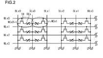
- FIG. 2is a circuit diagram showing a structure of the first memory layer 12 shown in FIG. 1 .
- the first memory layer 12includes a plurality of first bit lines BLx, a plurality of word lines WLx provided in a direction intersecting the first bit lines BLx, and a plurality of first source lines SLx provided in a direction along the first bit lines BLx.
- a first memory cell MCxis provided, and one end of the first memory cell MCx is coupled to one of the first bit lines BLx and the other end of the first memory cell MCx is coupled to one of the first source lines SLx.
- Two first memory cells MCx(for example, MCx0 and MCx1) adjacent to each other in the word lines WLx direction share a first source line SLx (for example, SLx0).
- a first source line SLxfor example, SLx0.
- the first memory cell MCxis composed of a first variable resistance element REx and a selection transistor TRx.
- a drain terminal of the selection transistor TRxis coupled to the first bit line BLx, a source terminal of the selection transistor is coupled to the first variable resistance element REx, and a gate terminal of the selection transistor is coupled to one of the word lines WLx.
- the other end of the first variable resistance element RExis coupled to the first source line SLx.
- the first memory cell MCxstores data by varying a resistance value of the first variable resistance element REx. For example, in a case where the first variable resistance element REx changes into either a high resistance state or a low resistance state, data of one bit can be stored per memory cell.
- the selection transistor TRselects the first variable resistance element REx by conducting the first variable resistance element REx and the first bit line BLx in accordance with a voltage applied to the gate terminal.
- FIG. 3is a top view schematically showing a structure of the first memory cell MCx of FIG. 2 .
- a P-type well and N-type diffusion regionsthat are both not shown are formed (see FIG. 4 ).
- a bit line contact 32is formed on the first bit line BLx
- a source line contact 34is formed on the first source line SLx, and they are respectively coupled to the diffusion regions formed below.
- the first variable resistance element RExis provided in the source line contact 34 .
- the selection transistor TRis provided in a region including the semiconductor substrate 30 corresponding to the bit line contact 32 and the source line contact 34 .
- a region between the first bit line BLx and the first source line SLx over the semiconductor substrate 30is provided with a gate electrode 36 of the selection transistor TR.
- the gate electrode 36is coupled to the word line WL by a word line contact 38 .
- the first memory cell MCxis formed in a region including the first variable resistance element REx and the selection transistor TR.
- the substantial size of the cellcorresponds to a region 39 in FIG. 3 .
- the cell area of the first memory cell MCxcan be 8F 2 to 9F 2 , for example.
- FIG. 4is a schematic cross-sectional view along the line A-A 1 in FIG. 3 .
- a p-type well 46is formed on the upper surface of the semiconductor substrate 30 made of, for example, silicon.
- N-type diffusion regions 40 and 41are formed in the P-type well 46 .
- the diffusion region 40is the drain terminal of the selection transistor TR, and is coupled to the first bit line BLx via the bit line contact 32 .
- the diffusion region 41is the source terminal of the selection transistor TR, and is coupled to the first source line SLx via the source line contact 34 .
- the first variable resistance element RExis provided in the source line contact 34 .
- the first variable resistance element RExis formed by using a resistance variation element made of transition metal oxide such as CuO 2 .
- phase-change materialssuch as ternary chalcogenide can be used. Either can arbitrarily vary the resistance value by applying a voltage pulse of a predetermined magnitude for a predetermined period of time.
- wirings of the first bit line BLx, the first source line SLx, and the word line WLxcan be formed with metals such as aluminum.
- the bit line contact 32 and the source line contact 34can be formed by using a conductive material 42 including metals such as tungsten. Note that the illustration of insulating materials such as a gate oxide film and an interlayer insulating film are omitted in FIG. 4 .
- the semiconductor deviceby using, for example, a diffusion process, a part of the selection transistor TR (drain terminal and source terminal) is formed in the semiconductor substrate. Accordingly, by effectively utilizing a region that normally serves as a bulk, the semiconductor device can be miniaturized. Also, since the first variable resistance element REx is formed in the source line contact 34 of the selection transistor TR, the first memory layer 12 has a structure in which a first variable resistance element layer 52 including the first variable resistance element REx is provided over a selection transistor layer 50 including the selection transistor TR. By adopting such a stacked structure, the area of the first memory cell MCx can be reduced.
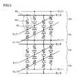
- FIG. 5is a circuit diagram showing a structure of the second memory layer 14 .
- FIG. 6is a perspective view showing a structure of a part of FIG. 5 .
- the second memory layer 14is provided with a plurality of second bit lines BLz and a plurality of second source lines SLz provided in a direction intersecting the second bit lines BLz.
- a second memory cell MCzis provided, and one end thereof is coupled to one of the second bit lines BLz and the other end thereof is coupled to one of the second source lines SLz.
- more than one such second memory cell MCzis arranged in a plane.
- a plurality of second memory layers 14 a to 14 dare stacked over the first memory layer 12 not shown.
- two vertically adjacent second memory layersshare either the second bit line BLz or the second source line SLz.
- the second memory layers 14 a and 14 bshare second source lines SLz10 and SLz11. Accordingly, high integration of the second memory layer can be further achieved.
- the second memory cell MCzis structured to consist of one second variable resistance element REz and one selection diode SD.
- a cathode side of the selection diode SDis coupled to the second source line SLz, and an anode side thereof is coupled in series with the second variable resistance element REz.
- the other end of the second variable resistance element REzis coupled to the second bit line BLz.
- the second memory cell MCzstores data by varying a resistance value of the second variable resistance element REz as in the case of the first memory cell MCx.
- the selection diode SDselects the second variable resistance element REz in accordance with a potential difference between the second bit line BLz and the second source line SLz.
- the second bit line BLzwhen not selected, the second bit line BLz is set to low level and the second source line SLz is set to high level, whereby the selection diode SD is applied with a reverse bias, and no electric current flows into the second variable resistance element REz.
- the second bit line BLzis set to high level and the second source line SLz is set to low level, whereby the selection diode SD is applied with a forward bias, and electric current flows into the second variable resistance element REz.
- FIG. 7is a cross-sectional view along the line B-B 1 in FIG. 6 .
- the second memory cell MCzis structured of the second variable resistance element REz and electrodes 60 provided on both ends thereof.
- the second variable resistance element REzcan be made of CuO 2 that is a transition metal oxide, and each electrode 60 can be made of Cu.
- a Schottky diode SD due to potential barrieris formed in a boundary of the second variable resistance element REz and the electrode 60 . This corresponds to the selection diode SD in FIG. 5 .
- the selection diode SDBy making the selection diode SD as a Schottky diode, the memory cell can be miniaturized relative to a case wherein a PN junction diode is used.
- the second memory cell MCzis structured by stacking the second variable resistance element REz and the selection diode SD in a stacking direction (vertical direction) of the first memory layer 12 and the second memory layer 14 .
- the second bit line BLz and the second source line SLzcan be formed of metal wirings such as aluminum.
- MIMmetal insulation metal
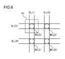
- FIG. 8is a top view of FIG. 6 .
- the second memory cell MCzIn the intersection region of the second bit lines BLz and the second source lines SLz, the second memory cell MCz is provided.
- the substantial size of the second memory cell MCzcorresponds to a region 62 , and is determined by the wiring width and the wiring spacing of the second bit lines BLz and the second source lines SLz.
- the second memory cell MCzuses a diode instead of a transistor for selecting a cell, whereby the area thereof is smaller than that of the first memory cell MCx when viewed in a stacking direction of the first memory layer 12 and the second memory layer 14 .
- the cell area of the second memory cell MCzis 4F 2 that is equal to or less than half of the area of the first memory cell MCx (8F 2 to 9F 2 ).
- the second memory cells MCzare arranged such that the upper and lower second memory cells MCz overlap with each other when viewed from a stacking direction of the first memory layer 12 and the second memory layer 14 .
- a stacking method of the second memory cells MCzis not limited to this.
- the second memory cellsfor example, MCz20 and MCz21
- the second memory cellsfor example, MCz10 and MCz11
- FIG. 9Ais a perspective view showing a structure of the second memory layer 14 having the second memory cells MCz arranged in such a manner.
- FIG. 9Bis a cross-sectional view along the line C-C 1 in FIG. 9A .
- the semiconductor deviceincludes the first memory cell MCx selected by the selection transistor TR and the second memory cell MCz selected by the selection diode SD.
- Selection by the selection transistor TRis performed by controlling a voltage applied to the gate terminal of the selection transistor TR, therefore controlling is easy and reliability is high. Accordingly, data-holding performance and reliability of the first memory cell MCx are excellent.
- the first memory cell MCxstores data of high importance (hereinafter, core data) such as a basic program such as an OS and a boot program read when turning on the power. Accordingly, operation stability of the semiconductor device according to the present embodiment and electronic equipment in which the semiconductor device according to the present embodiment is built-in can be improved.
- the selection of a memory cell by the selection diode SDis performed by controlling a voltage level of the bit line and the source line as explained with reference to FIG. 5 . Therefore, controlling is difficult compared to controlling by using the selection transistor TR, and the reliability is low. As a result, in the second memory cell MCz selected by the selection diode SD, disturbance and leakage or the like of data are liable to occur compared to the first memory cell MCx. On the other hand, since the second memory cells MCz can be stacked, and the cell area of each of the second memory cells MCz is smaller than the cell area of each of the first memory cells MCx, it is easy to increase the capacity of the second memory cell MCz. Accordingly, data which may be partially damaged (for example, text data or image data generated by a user) or a large amount of data (for example, audio data or moving image data) are stored in the second memory cell MCz.
- data which may be partially damagedfor example, text data or image data generated by a user
- datacan be stored efficiently by selectively using the first memory cell MCx and the second memory cell MCz (the first memory layer 12 and the second memory layer 14 ) in accordance with a characteristic of data. Consequently, the semiconductor device having a non-volatile memory can achieve an increase in storage capacity and improvement of operation reliability at the same time. Also, such semiconductor devices can easily be adapted to correspond to various applications.
- the semiconductor deviceadopts a structure in which the second memory layers 14 each including the second memory cell MCz are multiply stacked over the first memory layer 12 including the first memory cell MCx.
- the first memory layer 12includes the selection transistor TR
- the second memory layer 14includes the second variable resistance element REz and the selection diode SD formed in a vertical direction
- the second memory layer 14is suitable for stacking.
- the selection transistor TR included in the first memory layer 12can be formed in the semiconductor substrate, the second memory layer 14 cannot be formed directly on the semiconductor substrate.
- the first memory layer 12 having a capacity necessary for storing core datais formed in an area including the semiconductor substrate.
- the second memory layer 14 suitable to stackis formed thereon in accordance with a required memory storage capacity.
- adjacent first memory cells MCxshare the first source line SLx.
- vertically adjacent second memory cells MCzshare the second bit line BLz or the second source line SLz. Accordingly, by sharing a part of wirings between adjacent memory cells, the cell area can be reduced and the semiconductor device can be miniaturized.
- the selection transistor TRis coupled to the first bit line BLx, and the first variable resistance element REx is coupled to the first source line SLx.
- the arrangements of the twoare not limited thereto.
- the first variable resistance element RExcan be coupled to the first bit line BLx, and the selection transistor TR can be coupled to the first source line SLx.
- the selection diode SDis coupled to the second source line SLz, and the second variable resistance element REz is coupled to the second bit line BLz.
- the arrangement of the twois not limited thereto.
- the second variable resistance element REzcan be coupled to the second bit line BLz, and the selection diode SD can be coupled to the second source line SLz.
Landscapes
- Semiconductor Memories (AREA)
Abstract
Description
- This application claims priority from Japanese patent application 2007-270745 filed on Oct. 17, 2007
- The present invention relates to a semiconductor device including a non-volatile memory that is electrically erasable and writable.
- Recently, memory devices including non-volatile memory elements that store data by varying resistivity of variable resistors have been developed. Examples of such memory elements are a phase-change RAM (PRAM) that uses phase-change materials such as ternary chalcogenide, a colossal magnetoresistive effect (CMR) element that uses colossal magnetoresistance effects, and a resistive RAM (ReRAM) that uses variable resistance materials of transition metal oxide.
- Writing data to the above enumerated memory elements is preformed by applying a voltage pulse of a predetermined condition to variable resistors in the memory elements, thereby varying resistance values of the variable resistors. Access control of the memory elements is performed via memory selection elements coupled to the memory elements.
- Published Japanese Translation of PCT Application No. JP-T-2007-511895 discloses a conventional memory device that uses a transistor for a memory selection element. Published Japanese Translation of PCT Application No. JP-T-2005-522045 discloses a conventional memory device that uses a diode for a memory selection element. Japanese Patent Application Publication No. JP-A-2005-159359 discloses a conventional memory device that controls access to a memory element without using active elements such as a diode and a transistor.
- Conventional semiconductor devices typically use variable resistive memory transistors or diodes for memory selection elements. Memory devices using transistors for memory selection elements are easy to control, and also high in reliability. Therefore, such memory devices are superior in data-holding performance and rewiring resistance. However, there is a disadvantage that, since a relatively large area is necessary for forming transistors, high integration of memory elements is difficult. Therefore, such memory devices are suitable for storing data, such as a boot program read during start-up and an OS, which require high reliability, but not suitable for storing data of large capacity.
- Furthermore, memory devices using diodes for memory selection elements are suitable for increasing capacity since diodes can be formed in a smaller area compared to transistors and are also easier to stack vertically. However, access control to memory elements is performed by controlling a voltage level of bit lines and source lines coupled to the memory elements. Unfortunately, controlling the voltage can be difficult and unreliable. Accordingly, such memory devices are suitable for storing data with a large capacity such as moving image data or audio data, but unsuitable for storing important data on the other since their reliability is low and they are prone to cause problems such as disturbance and leakage. As such, in conventional memory devices, there is a problem that applicability thereof is limited depending on a characteristic of data to be stored.
- This Summary is provided to introduce a selection of concepts in a simplified form that are further described below in the Detailed Description. This Summary is not intended to identify key features or essential features of the claimed subject matter, nor is it intended to be used to limit the scope of the claimed subject matter.
- A semiconductor device according to an aspect of the present invention includes: a first memory cell including a non-volatile first variable resistance element that stores data by varying a resistance value and a selection transistor that selects the first variable resistance element; a first memory layer provided with a plurality of the first memory cells arranged in a plane; a second memory cell including a non-volatile second variable resistance element that stores data by varying a resistance value and a selection diode that selects the second variable resistance element; and a second memory layer provided with a plurality of second memory cells arranged in a plane. A plurality of second memory layers is stacked over the first memory layer. According to this aspect of the present invention, data can be stored efficiently by selectively using the first memory layer and the second memory layer depending on a characteristic of data to be stored. Therefore, an increase in storage capacity and improvement of operation stability can be achieved at the same time. Further, by adopting a structure in which the plurality of second memory layers are stacked over the first memory layer, miniaturization and cost reduction of the semiconductor device can be achieved.
- In this arrangement, the second memory cell may have the second variable resistance element and the selection diode stacked in a stacking direction of the first memory layer and the second memory layer. With this arrangement, high integration of the second memory layer can be further achieved.
- In this arrangement, the area of the second memory cell may be smaller than that of the first memory cell when seen from a stacking direction of the first memory layer and the second memory layer. With this arrangement, high integration of the second memory layer can be further achieved.
- In this arrangement, the second memory layer may include: a plurality of second bit lines; and a plurality of second word lines provided in a direction intersecting the plurality of second bit lines. The second memory cell may be provided in an intersection region of the second bit lines and the second word lines, one end thereof being coupled to one of the second bit lines and the other end thereof being coupled to one of the second word lines. Two vertically adjacent second memory layers among the plurality of second memory layers may share either the second bit line or the second word line. With this arrangement, the second memory layers can be formed thinner by sharing the second word line or the second bit line. Therefore, high integration of the second memory layer can be further achieved.
- In this arrangement, of the two vertically adjacent second memory layers among the plurality of second memory layers, the second memory cell included in an upper layer and the second memory cell included in a lower layer may be provided being shifted for a half of a minimum machining dimension.
- In this arrangement, the first memory cell may include: one such selection transistor; and one such first variable resistance element coupled to a drain terminal or a source terminal of the selection transistor. With this arrangement, since one such first variable resistance element is selected by one such selection transistor, operation reliability of the first memory cell can be improved.
- In this arrangement, the semiconductor device may also include a semiconductor substrate supporting the first memory layer and the second memory layer. At least a part of the selection transistor is formed in the semiconductor substrate. With this arrangement, by effectively using the space of the semiconductor substrate, high integration of the first memory layer can be further achieved.
- In this arrangement, the first memory layer may include: a selection transistor layer including the selection transistor; and a first variable resistance element layer including the first variable resistance element, the first variable resistance element layer being formed over the selection transistor layer. With this arrangement, since the first memory cells are formed vertically, high integration of the first memory layer can be further achieved.
- In this arrangement, the first memory layer may include: a plurality of first bit lines; a plurality of first word lines provided in a direction intersecting the plurality of first bit lines; and a plurality of source lines provided in a direction along the plurality of first bit lines. The first memory cell is provided in an intersection region of the first bit lines and the first word lines, one end thereof being coupled to one of the first bit lines and the other end thereof being coupled to one of the source lines. Two adjacent first memory cells among the plurality of first memory cells share the source line. With this arrangement, since adjacent two first memory cells share the source line, high integration of the first memory layer can be further achieved.
- In this arrangement, the variable resistance element may be made of transition metal oxide.
- In this arrangement, the selection diode may be a Schottky diode made of the transition metal oxide and a metal electrode. With this arrangement, compared to a case of using a PN junction diode, the second memory cell can be miniaturized.
- In this arrangement, the first memory cell may store data including at least one of a boot program read when turning on the power and an operating system (OS) program. With this arrangement, by storing the boot program or the OS program in the first memory cell having high operation reliability, operation stability of the semiconductor device can be improved.
- The above-mentioned semiconductor device includes the first memory layer excellent in reliability of holding data and the second memory layer having large storage capacity. By selectively using these layers, data can be stored efficiently. Thereby, an increase in storage capacity and improvement of operation stability can be achieved at the same time. Further, by stacking the first memory layer and the second memory layer in a vertical direction, miniaturization and cost reduction of the semiconductor device can be achieved.
- While the preferred embodiment of the present invention is described in details above, the present invention is not limited to the specific embodiment and, within the spirit and scope of the present invention as defined in the appended claims, various modifications and alterations may naturally be made.
- The accompanying drawings, which are incorporated in and form a part of this specification, illustrate embodiments of the invention and, together with the description, serve to explain the principles of the invention:
FIG. 1 is a block diagram showing a structure of a semiconductor device according to a first embodiment of the present invention;FIG. 2 is a circuit diagram showing a structure of a first memory layer;FIG. 3 is a top view showing the structure of the first memory layer;FIG. 4 is a cross-sectional view showing the structure of the first memory layer;FIG. 5 is a circuit diagram showing a structure of a second memory layer;FIG. 6 is a perspective view showing the structure of the second memory layer;FIG. 7 is a cross-sectional view showing the structure of the second memory layer;FIG. 8 is a top view showing the structure of the second memory layer; andFIG. 9A is a perspective view showing a structure of an alternative mode of the second memory layer, andFIG. 9B is a cross-sectional view showing a structure of an alternative mode of the second memory layer.- Reference will now be made in detail to the preferred embodiments of the claimed subject matter, a method and system for the use of a reputation service provider, examples of which are illustrated in the accompanying drawings. While the claimed subject matter will be described in conjunction with the preferred embodiments, it will be understood that they are not intended to be limit to these embodiments. On the contrary, the claimed subject matter is intended to cover alternatives, modifications and equivalents, which may be included within the spirit and scope as defined by the appended claims.
- Furthermore, in the following detailed descriptions of embodiments of the claimed subject matter, numerous specific details are set forth in order to provide a thorough understanding of the claimed subject matter. However, it will be recognized by one of ordinary skill in the art that the claimed subject matter may be practiced without these specific details. In other instances, well known methods, procedures, components, and circuits have not been described in detail as not to unnecessarily obscure aspects of the claimed subject matter.
FIG. 1 is a block diagram showing a structure of a semiconductor device according to one embodiment of the present invention. As depicted inFIG. 1 , amemory 10 that is a region for storing data includes two storage regions of afirst memory layer 12 and asecond memory layer 14. Thememory 10 has a three-dimensional structure, and a plurality of the second memory layers14 is stacked over thefirst memory layer 12. Acontroller 20 controls, in accordance with a command input from the outside, anaddress decoder 22, abooster circuit 24, and an input/output section 26, and controls writing and reading of data to/from thememory 10. Theaddress decoder 22 selects a memory cell in thememory 10 in accordance with an address signal input from the outside. Thebooster circuit 24 provides a high voltage to thememory 10 for writing data. The input/output section 26 exchanges data between the outside and thememory 10.FIG. 2 is a circuit diagram showing a structure of thefirst memory layer 12 shown inFIG. 1 . Thefirst memory layer 12 includes a plurality of first bit lines BLx, a plurality of word lines WLx provided in a direction intersecting the first bit lines BLx, and a plurality of first source lines SLx provided in a direction along the first bit lines BLx. In each intersection region of the first bit lines BLx and the word lines WLx, a first memory cell MCx is provided, and one end of the first memory cell MCx is coupled to one of the first bit lines BLx and the other end of the first memory cell MCx is coupled to one of the first source lines SLx. Two first memory cells MCx (for example, MCx0 and MCx1) adjacent to each other in the word lines WLx direction share a first source line SLx (for example, SLx0). As described above, in thefirst memory layer 12, more than one such first memory cell MCx is arranged in a plane. The number of the first memory cells MCx may be arbitrary depending on storage capacity.- The first memory cell MCx is composed of a first variable resistance element REx and a selection transistor TRx. A drain terminal of the selection transistor TRx is coupled to the first bit line BLx, a source terminal of the selection transistor is coupled to the first variable resistance element REx, and a gate terminal of the selection transistor is coupled to one of the word lines WLx. The other end of the first variable resistance element REx is coupled to the first source line SLx. The first memory cell MCx stores data by varying a resistance value of the first variable resistance element REx. For example, in a case where the first variable resistance element REx changes into either a high resistance state or a low resistance state, data of one bit can be stored per memory cell. The selection transistor TR selects the first variable resistance element REx by conducting the first variable resistance element REx and the first bit line BLx in accordance with a voltage applied to the gate terminal.
FIG. 3 is a top view schematically showing a structure of the first memory cell MCx ofFIG. 2 . On an upper surface of asemiconductor substrate 30 supporting thefirst memory layer 12 and thesecond memory layer 14, a P-type well and N-type diffusion regions that are both not shown are formed (seeFIG. 4 ). Abit line contact 32 is formed on the first bit line BLx, asource line contact 34 is formed on the first source line SLx, and they are respectively coupled to the diffusion regions formed below. The first variable resistance element REx is provided in thesource line contact 34. The selection transistor TR is provided in a region including thesemiconductor substrate 30 corresponding to thebit line contact 32 and thesource line contact 34. A region between the first bit line BLx and the first source line SLx over thesemiconductor substrate 30 is provided with agate electrode 36 of the selection transistor TR. Thegate electrode 36 is coupled to the word line WL by aword line contact 38.- The first memory cell MCx is formed in a region including the first variable resistance element REx and the selection transistor TR. The substantial size of the cell corresponds to a
region 39 inFIG. 3 . In a case where the minimum machining dimension is defined as F, the cell area of the first memory cell MCx can be 8F2to 9F2, for example. FIG. 4 is a schematic cross-sectional view along the line A-A1 inFIG. 3 . A p-type well 46 is formed on the upper surface of thesemiconductor substrate 30 made of, for example, silicon. N-type diffusion regions type well 46. Thediffusion region 40 is the drain terminal of the selection transistor TR, and is coupled to the first bit line BLx via thebit line contact 32. Thediffusion region 41 is the source terminal of the selection transistor TR, and is coupled to the first source line SLx via thesource line contact 34. In thesource line contact 34, the first variable resistance element REx is provided. The first variable resistance element REx is formed by using a resistance variation element made of transition metal oxide such as CuO2. Further, phase-change materials such as ternary chalcogenide can be used. Either can arbitrarily vary the resistance value by applying a voltage pulse of a predetermined magnitude for a predetermined period of time. Further, wirings of the first bit line BLx, the first source line SLx, and the word line WLx can be formed with metals such as aluminum. Thebit line contact 32 and thesource line contact 34 can be formed by using aconductive material 42 including metals such as tungsten. Note that the illustration of insulating materials such as a gate oxide film and an interlayer insulating film are omitted inFIG. 4 .- In this embodiment, by using, for example, a diffusion process, a part of the selection transistor TR (drain terminal and source terminal) is formed in the semiconductor substrate. Accordingly, by effectively utilizing a region that normally serves as a bulk, the semiconductor device can be miniaturized. Also, since the first variable resistance element REx is formed in the
source line contact 34 of the selection transistor TR, thefirst memory layer 12 has a structure in which a first variableresistance element layer 52 including the first variable resistance element REx is provided over aselection transistor layer 50 including the selection transistor TR. By adopting such a stacked structure, the area of the first memory cell MCx can be reduced. FIG. 5 is a circuit diagram showing a structure of thesecond memory layer 14.FIG. 6 is a perspective view showing a structure of a part ofFIG. 5 . Thesecond memory layer 14 is provided with a plurality of second bit lines BLz and a plurality of second source lines SLz provided in a direction intersecting the second bit lines BLz. In each intersection region of the second bit lines BLz and the second source lines SLz, a second memory cell MCz is provided, and one end thereof is coupled to one of the second bit lines BLz and the other end thereof is coupled to one of the second source lines SLz. As described above, more than one such second memory cell MCz is arranged in a plane. With reference toFIG. 5 , a plurality of second memory layers14ato14dare stacked over thefirst memory layer 12 not shown. Among the plurality of second memory layers14ato14d, two vertically adjacent second memory layers share either the second bit line BLz or the second source line SLz. For example, the second memory layers14aand14bshare second source lines SLz10 and SLz11. Accordingly, high integration of the second memory layer can be further achieved.- With reference to
FIG. 5 , the second memory cell MCz is structured to consist of one second variable resistance element REz and one selection diode SD. A cathode side of the selection diode SD is coupled to the second source line SLz, and an anode side thereof is coupled in series with the second variable resistance element REz. The other end of the second variable resistance element REz is coupled to the second bit line BLz. The second memory cell MCz stores data by varying a resistance value of the second variable resistance element REz as in the case of the first memory cell MCx. The selection diode SD selects the second variable resistance element REz in accordance with a potential difference between the second bit line BLz and the second source line SLz. In other words, when not selected, the second bit line BLz is set to low level and the second source line SLz is set to high level, whereby the selection diode SD is applied with a reverse bias, and no electric current flows into the second variable resistance element REz. When selected, the second bit line BLz is set to high level and the second source line SLz is set to low level, whereby the selection diode SD is applied with a forward bias, and electric current flows into the second variable resistance element REz. FIG. 7 is a cross-sectional view along the line B-B1 inFIG. 6 . The second memory cell MCz is structured of the second variable resistance element REz andelectrodes 60 provided on both ends thereof. By way of example, the second variable resistance element REz can be made of CuO2that is a transition metal oxide, and eachelectrode 60 can be made of Cu. Accordingly, a Schottky diode SD due to potential barrier is formed in a boundary of the second variable resistance element REz and theelectrode 60. This corresponds to the selection diode SD inFIG. 5 . By making the selection diode SD as a Schottky diode, the memory cell can be miniaturized relative to a case wherein a PN junction diode is used. Accordingly, the second memory cell MCz is structured by stacking the second variable resistance element REz and the selection diode SD in a stacking direction (vertical direction) of thefirst memory layer 12 and thesecond memory layer 14. Further, the second bit line BLz and the second source line SLz can be formed of metal wirings such as aluminum. As described above, by adopting a metal insulation metal (MIM) structure in which metals and insulators are stacked alternately, the memory cell can be easily stacked in the vertical direction.FIG. 8 is a top view ofFIG. 6 . In the intersection region of the second bit lines BLz and the second source lines SLz, the second memory cell MCz is provided. The substantial size of the second memory cell MCz corresponds to aregion 62, and is determined by the wiring width and the wiring spacing of the second bit lines BLz and the second source lines SLz. The second memory cell MCz uses a diode instead of a transistor for selecting a cell, whereby the area thereof is smaller than that of the first memory cell MCx when viewed in a stacking direction of thefirst memory layer 12 and thesecond memory layer 14. In a case where the minimum machining dimension is defined as F, the cell area of the second memory cell MCz is 4F2that is equal to or less than half of the area of the first memory cell MCx (8F2to 9F2).- In
FIG. 6 toFIG. 8 , the second memory cells MCz are arranged such that the upper and lower second memory cells MCz overlap with each other when viewed from a stacking direction of thefirst memory layer 12 and thesecond memory layer 14. However, a stacking method of the second memory cells MCz is not limited to this. For example, among vertically adjacent two second memory layers14, the second memory cells (for example, MCz20 and MCz21) included in an upper layer and the second memory cells (for example, MCz10 and MCz11) included in a lower layer can be provided being shifted for a half of the minimum machining dimension F.FIG. 9A is a perspective view showing a structure of thesecond memory layer 14 having the second memory cells MCz arranged in such a manner.FIG. 9B is a cross-sectional view along the line C-C1 inFIG. 9A . - The semiconductor device according to the present embodiment of the present invention includes the first memory cell MCx selected by the selection transistor TR and the second memory cell MCz selected by the selection diode SD. Selection by the selection transistor TR is performed by controlling a voltage applied to the gate terminal of the selection transistor TR, therefore controlling is easy and reliability is high. Accordingly, data-holding performance and reliability of the first memory cell MCx are excellent. The first memory cell MCx stores data of high importance (hereinafter, core data) such as a basic program such as an OS and a boot program read when turning on the power. Accordingly, operation stability of the semiconductor device according to the present embodiment and electronic equipment in which the semiconductor device according to the present embodiment is built-in can be improved.
- The selection of a memory cell by the selection diode SD is performed by controlling a voltage level of the bit line and the source line as explained with reference to
FIG. 5 . Therefore, controlling is difficult compared to controlling by using the selection transistor TR, and the reliability is low. As a result, in the second memory cell MCz selected by the selection diode SD, disturbance and leakage or the like of data are liable to occur compared to the first memory cell MCx. On the other hand, since the second memory cells MCz can be stacked, and the cell area of each of the second memory cells MCz is smaller than the cell area of each of the first memory cells MCx, it is easy to increase the capacity of the second memory cell MCz. Accordingly, data which may be partially damaged (for example, text data or image data generated by a user) or a large amount of data (for example, audio data or moving image data) are stored in the second memory cell MCz. - Accordingly, data can be stored efficiently by selectively using the first memory cell MCx and the second memory cell MCz (the
first memory layer 12 and the second memory layer14) in accordance with a characteristic of data. Consequently, the semiconductor device having a non-volatile memory can achieve an increase in storage capacity and improvement of operation reliability at the same time. Also, such semiconductor devices can easily be adapted to correspond to various applications. - The semiconductor device according to the present embodiment of the present invention adopts a structure in which the second memory layers14 each including the second memory cell MCz are multiply stacked over the
first memory layer 12 including the first memory cell MCx. As described above, since thefirst memory layer 12 includes the selection transistor TR, thefirst memory layer 12 may be unsuitable for stacking. On the other hand, since thesecond memory layer 14 includes the second variable resistance element REz and the selection diode SD formed in a vertical direction, thesecond memory layer 14 is suitable for stacking. Further, although a part of the selection transistor TR included in thefirst memory layer 12 can be formed in the semiconductor substrate, thesecond memory layer 14 cannot be formed directly on the semiconductor substrate. Therefore, at first, thefirst memory layer 12 having a capacity necessary for storing core data is formed in an area including the semiconductor substrate. Then, thesecond memory layer 14 suitable to stack is formed thereon in accordance with a required memory storage capacity. By adopting such three-dimensional structure, thememory area 10 can be structured in the most efficient manner. As a result, miniaturization and cost reduction of the semiconductor device can be achieved. - Further, with reference to
FIG. 2 , adjacent first memory cells MCx share the first source line SLx. With reference toFIG. 5 , vertically adjacent second memory cells MCz share the second bit line BLz or the second source line SLz. Accordingly, by sharing a part of wirings between adjacent memory cells, the cell area can be reduced and the semiconductor device can be miniaturized. - In
FIG. 2 , the selection transistor TR is coupled to the first bit line BLx, and the first variable resistance element REx is coupled to the first source line SLx. However, the arrangements of the two are not limited thereto. For example, the first variable resistance element REx can be coupled to the first bit line BLx, and the selection transistor TR can be coupled to the first source line SLx. Further, as shown inFIG. 5 , the selection diode SD is coupled to the second source line SLz, and the second variable resistance element REz is coupled to the second bit line BLz. However, the arrangement of the two is not limited thereto. For example, the second variable resistance element REz can be coupled to the second bit line BLz, and the selection diode SD can be coupled to the second source line SLz. - Although the subject matter has been described in language specific to structural features and/or methodological acts, it is to be understood that the subject matter defined in the appended claims is not necessarily limited to the specific features or acts described above. Rather, the specific features and acts described above are disclosed as example forms of implementing the claims.
Claims (10)
Priority Applications (2)
| Application Number | Priority Date | Filing Date | Title |
|---|---|---|---|
| US13/005,456US8289750B2 (en) | 2007-10-17 | 2011-01-12 | Semiconductor memory device featuring selective data storage in a stacked memory cell structure |
| US13/622,796US8773885B2 (en) | 2007-10-17 | 2012-09-19 | Semiconductor memory device featuring selective data storage in a stacked memory cell structure |
Applications Claiming Priority (2)
| Application Number | Priority Date | Filing Date | Title |
|---|---|---|---|
| JP2007270745AJP5557419B2 (en) | 2007-10-17 | 2007-10-17 | Semiconductor device |
| JP2007-270745 | 2007-10-17 |
Related Child Applications (1)
| Application Number | Title | Priority Date | Filing Date |
|---|---|---|---|
| US13/005,456ContinuationUS8289750B2 (en) | 2007-10-17 | 2011-01-12 | Semiconductor memory device featuring selective data storage in a stacked memory cell structure |
Publications (2)
| Publication Number | Publication Date |
|---|---|
| US20090262569A1true US20090262569A1 (en) | 2009-10-22 |
| US7894238B2 US7894238B2 (en) | 2011-02-22 |
Family
ID=40702527
Family Applications (3)
| Application Number | Title | Priority Date | Filing Date |
|---|---|---|---|
| US12/253,619Active2029-09-04US7894238B2 (en) | 2007-10-17 | 2008-10-17 | Semiconductor memory device with stacked memory cell structure |
| US13/005,456ActiveUS8289750B2 (en) | 2007-10-17 | 2011-01-12 | Semiconductor memory device featuring selective data storage in a stacked memory cell structure |
| US13/622,796ActiveUS8773885B2 (en) | 2007-10-17 | 2012-09-19 | Semiconductor memory device featuring selective data storage in a stacked memory cell structure |
Family Applications After (2)
| Application Number | Title | Priority Date | Filing Date |
|---|---|---|---|
| US13/005,456ActiveUS8289750B2 (en) | 2007-10-17 | 2011-01-12 | Semiconductor memory device featuring selective data storage in a stacked memory cell structure |
| US13/622,796ActiveUS8773885B2 (en) | 2007-10-17 | 2012-09-19 | Semiconductor memory device featuring selective data storage in a stacked memory cell structure |
Country Status (2)
| Country | Link |
|---|---|
| US (3) | US7894238B2 (en) |
| JP (1) | JP5557419B2 (en) |
Cited By (5)
| Publication number | Priority date | Publication date | Assignee | Title |
|---|---|---|---|---|
| US20090289251A1 (en)* | 2008-05-22 | 2009-11-26 | Masahiro Kiyotoshi | Nonvolatile memory device and method for manufacturing same |
| US20140183438A1 (en)* | 2010-02-09 | 2014-07-03 | Sony Corporation | Memory component, memory device, and method of operating memory device |
| US20150117088A1 (en)* | 2013-10-29 | 2015-04-30 | Kabushiki Kaisha Toshiba | Non-volatile memory device |
| US10861503B1 (en)* | 2019-06-27 | 2020-12-08 | SK Hynix Inc. | Electronic device |
| US11636895B2 (en)* | 2019-11-05 | 2023-04-25 | Samsung Electronics Co., Ltd. | Non-volatile resistive memory device including a plurality of write modes |
Families Citing this family (11)
| Publication number | Priority date | Publication date | Assignee | Title |
|---|---|---|---|---|
| US20070192132A1 (en) | 2006-02-10 | 2007-08-16 | Debra Thesman | System and method of prioritizing and administering healthcare to patients having multiple integral diagnoses |
| JP5557419B2 (en) | 2007-10-17 | 2014-07-23 | スパンション エルエルシー | Semiconductor device |
| US8223525B2 (en)* | 2009-12-15 | 2012-07-17 | Sandisk 3D Llc | Page register outside array and sense amplifier interface |
| US8477524B2 (en) | 2009-12-25 | 2013-07-02 | Samsung Electronics Co., Ltd. | Nonvolatile memory devices and related methods and systems |
| JP5295991B2 (en)* | 2010-02-15 | 2013-09-18 | 株式会社東芝 | Nonvolatile semiconductor memory device and control method of nonvolatile semiconductor memory device |
| KR20120114611A (en)* | 2011-04-07 | 2012-10-17 | 에스케이하이닉스 주식회사 | Semiconductor memory apparatus having magnetroresistive memory elements and method of manufacturing the same |
| US20120329015A1 (en) | 2011-06-24 | 2012-12-27 | Debra Thesman | Hierarchical condition categories program |
| US10424032B2 (en) | 2012-12-12 | 2019-09-24 | Quality Standards, Llc | Methods for administering preventative healthcare to a patient population |
| KR102001466B1 (en)* | 2013-09-25 | 2019-07-18 | 에스케이하이닉스 주식회사 | Electronic device |
| US9443590B2 (en) | 2014-10-13 | 2016-09-13 | Sandisk Technologies Llc | Content addressable memory cells, memory arrays and methods of forming the same |
| US9691475B2 (en)* | 2015-03-19 | 2017-06-27 | Micron Technology, Inc. | Constructions comprising stacked memory arrays |
Citations (53)
| Publication number | Priority date | Publication date | Assignee | Title |
|---|---|---|---|---|
| US5091966A (en)* | 1990-07-31 | 1992-02-25 | Xerox Corporation | Adaptive scaling for decoding spatially periodic self-clocking glyph shape codes |
| US5168147A (en)* | 1990-07-31 | 1992-12-01 | Xerox Corporation | Binary image processing for decoding self-clocking glyph shape codes |
| US5221833A (en)* | 1991-12-27 | 1993-06-22 | Xerox Corporation | Methods and means for reducing bit error rates in reading self-clocking glyph codes |
| US5245165A (en)* | 1991-12-27 | 1993-09-14 | Xerox Corporation | Self-clocking glyph code for encoding dual bit digital values robustly |
| US5315098A (en)* | 1990-12-27 | 1994-05-24 | Xerox Corporation | Methods and means for embedding machine readable digital data in halftone images |
| US5321773A (en)* | 1991-12-10 | 1994-06-14 | Xerox Corporation | Image recognition method using finite state networks |
| US5444779A (en)* | 1993-10-18 | 1995-08-22 | Xerox Corporation | Electronic copyright royalty accounting system using glyphs |
| US5449896A (en)* | 1993-12-22 | 1995-09-12 | Xerox Corporation | Random access techniques for use with self-clocking glyph codes |
| US5449895A (en)* | 1993-12-22 | 1995-09-12 | Xerox Corporation | Explicit synchronization for self-clocking glyph codes |
| US5453605A (en)* | 1993-12-22 | 1995-09-26 | Xerox Corporation | Global addressability for self-clocking glyph codes |
| US5486686A (en)* | 1990-05-30 | 1996-01-23 | Xerox Corporation | Hardcopy lossless data storage and communications for electronic document processing systems |
| US5526444A (en)* | 1991-12-10 | 1996-06-11 | Xerox Corporation | Document image decoding using modified branch-and-bound methods |
| US5572010A (en)* | 1995-01-03 | 1996-11-05 | Xerox Corporation | Distributed type labeling for embedded data blocks |
| US5576532A (en)* | 1995-01-03 | 1996-11-19 | Xerox Corporation | Interleaved and interlaced sync codes and address codes for self-clocking glyph codes |
| US5611575A (en)* | 1995-01-03 | 1997-03-18 | Xerox Corporation | Distributed state flags or other unordered information for embedded data blocks |
| US5825933A (en)* | 1996-12-20 | 1998-10-20 | Xerox Corporation | Parallel propagating embedded binary sequence for parameterizing two dimensional image domain code patterns in two dimensional address space |
| US5842191A (en)* | 1994-12-12 | 1998-11-24 | Xerox Corporation | Neural network that incorporates direct optical imaging |
| US5862255A (en)* | 1996-06-18 | 1999-01-19 | Xerox Corporation | Broad bandwidth image domain communication channel with symbol interference suppression |
| US5862271A (en)* | 1996-12-20 | 1999-01-19 | Xerox Corporation | Parallel propagating embedded binary sequences for characterizing and parameterizing two dimensional image domain code patterns in N-dimensional address space |
| US5864127A (en)* | 1996-10-10 | 1999-01-26 | Xerox Corporation | Analog glyph detector and detector arrays |
| US5870510A (en)* | 1996-12-20 | 1999-02-09 | Xerox Corporation | Parallel propagating embedded binary sequences for parameterizing two dimensional image domain code patterns in N-dimensional address space |
| US5883986A (en)* | 1995-06-02 | 1999-03-16 | Xerox Corporation | Method and system for automatic transcription correction |
| US5901224A (en)* | 1996-10-21 | 1999-05-04 | Xerox Corporation | Quasi-reprographics with variable embedded data with applications to copyright management, and distribution control |
| US5929429A (en)* | 1995-01-03 | 1999-07-27 | Xerox Corporation | Distributed dimensional labeling for dimensional characterization of border-type embedded data blocks |
| US5937110A (en)* | 1996-12-20 | 1999-08-10 | Xerox Corporation | Parallel propagating embedded binary sequences for characterizing objects in N-dimensional address space |
| US5939703A (en)* | 1995-01-03 | 1999-08-17 | Xerox Corporation | Distributed dimensional labeling for dimensional characterization of embedded data blocks |
| US5949055A (en)* | 1997-10-23 | 1999-09-07 | Xerox Corporation | Automatic geometric image transformations using embedded signals |
| US6000621A (en)* | 1995-12-21 | 1999-12-14 | Xerox Corporation | Tilings of mono-code and dual-code embedded data pattern strips for robust asynchronous capture |
| US6000613A (en)* | 1991-12-27 | 1999-12-14 | Xerox Corporation | Self-clocking glyph code having composite glyphs for distributively encoding multi-bit digital values |
| US6076738A (en)* | 1990-07-31 | 2000-06-20 | Xerox Corporation | Self-clocking glyph shape codes |
| US6182901B1 (en)* | 1993-12-22 | 2001-02-06 | Xerox Corporation | Orientational disambiguation for self-clocking glyph codes |
| US6296192B1 (en)* | 1999-12-16 | 2001-10-02 | Xerox Corporation | Machine-readable record with a two-dimensional lattice of synchronization code interleaved with data code |
| US20010045645A1 (en)* | 2000-04-20 | 2001-11-29 | Kabushiki Kaisha Toshiba | Multichip semiconductor device and memory card |
| US6327395B1 (en)* | 1996-12-20 | 2001-12-04 | Xerox Parc | Glyph address carpet methods and apparatus for providing location information in a multidimensional address space |
| US6340118B1 (en)* | 1999-12-16 | 2002-01-22 | Xerox Corporation | Exclusive or cross-coupled framing codes for self-clocking glyphs |
| US6360951B1 (en)* | 1999-12-16 | 2002-03-26 | Xerox Corporation | Hand-held scanning system for heuristically organizing scanned information |
| US6427920B1 (en)* | 1999-09-24 | 2002-08-06 | Xerox Corporation | High frequency masking of embedded digital data to improve appearance |
| US6439465B1 (en)* | 1999-09-24 | 2002-08-27 | Xerox Corporation | Encoding small amounts of embedded digital data at arbitrary locations within an image |
| US6448661B1 (en)* | 2001-02-09 | 2002-09-10 | Samsung Electornics Co., Ltd. | Three-dimensional multi-chip package having chip selection pads and manufacturing method thereof |
| US6594406B1 (en)* | 1996-12-20 | 2003-07-15 | Xerox Corporation | Multi-level selection methods and apparatus using context identification for embedded data graphical user interfaces |
| US6641051B1 (en)* | 1999-09-24 | 2003-11-04 | Xerox Corporation | System for embedded digital data that allows embedding of data around known obstructions |
| US6641053B1 (en)* | 2002-10-16 | 2003-11-04 | Xerox Corp. | Foreground/background document processing with dataglyphs |
| US6678425B1 (en)* | 1999-12-06 | 2004-01-13 | Xerox Corporation | Method and apparatus for decoding angular orientation of lattice codes |
| US6678415B1 (en)* | 2000-05-12 | 2004-01-13 | Xerox Corporation | Document image decoding using an integrated stochastic language model |
| US6714677B1 (en)* | 1999-12-17 | 2004-03-30 | Xerox Corporation | Use of correlation histograms for improved glyph decoding |
| US6738518B1 (en)* | 2000-05-12 | 2004-05-18 | Xerox Corporation | Document image decoding using text line column-based heuristic scoring |
| US6783069B1 (en)* | 1999-12-06 | 2004-08-31 | Xerox Corporation | Method and apparatus for implementing a camera mouse |
| US6839260B2 (en)* | 2000-01-18 | 2005-01-04 | Hitachi, Ltd. | Semiconductor device having different types of memory cell arrays stacked in a vertical direction |
| US6880755B2 (en)* | 1999-12-06 | 2005-04-19 | Xerox Coporation | Method and apparatus for display of spatially registered information using embedded data |
| USRE38758E1 (en)* | 1990-07-31 | 2005-07-19 | Xerox Corporation | Self-clocking glyph shape codes |
| US20060233012A1 (en)* | 2005-03-30 | 2006-10-19 | Elpida Memory, Inc. | Semiconductor storage device having a plurality of stacked memory chips |
| US20070132049A1 (en)* | 2005-12-12 | 2007-06-14 | Stipe Barry C | Unipolar resistance random access memory (RRAM) device and vertically stacked architecture |
| US20080110995A1 (en)* | 2006-10-31 | 2008-05-15 | Xerox Corporation | Method for embedding machine-readable information with fluorescent materials |
Family Cites Families (8)
| Publication number | Priority date | Publication date | Assignee | Title |
|---|---|---|---|---|
| JPH11134877A (en)* | 1997-10-28 | 1999-05-21 | Sharp Corp | Microcomputer with built-in nonvolatile storage |
| JP2003249578A (en)* | 2001-09-29 | 2003-09-05 | Toshiba Corp | Semiconductor integrated circuit device |
| AU2003201760A1 (en)* | 2002-04-04 | 2003-10-20 | Kabushiki Kaisha Toshiba | Phase-change memory device |
| JP4541651B2 (en)* | 2003-03-13 | 2010-09-08 | シャープ株式会社 | Resistance change function body, memory, manufacturing method thereof, semiconductor device, and electronic apparatus |
| US7408212B1 (en)* | 2003-07-18 | 2008-08-05 | Winbond Electronics Corporation | Stackable resistive cross-point memory with schottky diode isolation |
| WO2007046144A1 (en)* | 2005-10-19 | 2007-04-26 | Fujitsu Limited | Resistive memory element and its manufacturing method and nonvolatile semiconductor memory device |
| KR101176542B1 (en)* | 2006-03-02 | 2012-08-24 | 삼성전자주식회사 | Nonvolatile memory device and memory array |
| JP5557419B2 (en)* | 2007-10-17 | 2014-07-23 | スパンション エルエルシー | Semiconductor device |
- 2007
- 2007-10-17JPJP2007270745Apatent/JP5557419B2/enactiveActive
- 2008
- 2008-10-17USUS12/253,619patent/US7894238B2/enactiveActive
- 2011
- 2011-01-12USUS13/005,456patent/US8289750B2/enactiveActive
- 2012
- 2012-09-19USUS13/622,796patent/US8773885B2/enactiveActive
Patent Citations (55)
| Publication number | Priority date | Publication date | Assignee | Title |
|---|---|---|---|---|
| US5486686A (en)* | 1990-05-30 | 1996-01-23 | Xerox Corporation | Hardcopy lossless data storage and communications for electronic document processing systems |
| USRE38758E1 (en)* | 1990-07-31 | 2005-07-19 | Xerox Corporation | Self-clocking glyph shape codes |
| US5168147A (en)* | 1990-07-31 | 1992-12-01 | Xerox Corporation | Binary image processing for decoding self-clocking glyph shape codes |
| US5091966A (en)* | 1990-07-31 | 1992-02-25 | Xerox Corporation | Adaptive scaling for decoding spatially periodic self-clocking glyph shape codes |
| US6076738A (en)* | 1990-07-31 | 2000-06-20 | Xerox Corporation | Self-clocking glyph shape codes |
| US5315098A (en)* | 1990-12-27 | 1994-05-24 | Xerox Corporation | Methods and means for embedding machine readable digital data in halftone images |
| US5321773A (en)* | 1991-12-10 | 1994-06-14 | Xerox Corporation | Image recognition method using finite state networks |
| US5526444A (en)* | 1991-12-10 | 1996-06-11 | Xerox Corporation | Document image decoding using modified branch-and-bound methods |
| US5245165A (en)* | 1991-12-27 | 1993-09-14 | Xerox Corporation | Self-clocking glyph code for encoding dual bit digital values robustly |
| US6000613A (en)* | 1991-12-27 | 1999-12-14 | Xerox Corporation | Self-clocking glyph code having composite glyphs for distributively encoding multi-bit digital values |
| US5221833A (en)* | 1991-12-27 | 1993-06-22 | Xerox Corporation | Methods and means for reducing bit error rates in reading self-clocking glyph codes |
| US5444779A (en)* | 1993-10-18 | 1995-08-22 | Xerox Corporation | Electronic copyright royalty accounting system using glyphs |
| US6182901B1 (en)* | 1993-12-22 | 2001-02-06 | Xerox Corporation | Orientational disambiguation for self-clocking glyph codes |
| US5453605A (en)* | 1993-12-22 | 1995-09-26 | Xerox Corporation | Global addressability for self-clocking glyph codes |
| US5449895A (en)* | 1993-12-22 | 1995-09-12 | Xerox Corporation | Explicit synchronization for self-clocking glyph codes |
| US5449896A (en)* | 1993-12-22 | 1995-09-12 | Xerox Corporation | Random access techniques for use with self-clocking glyph codes |
| US5842191A (en)* | 1994-12-12 | 1998-11-24 | Xerox Corporation | Neural network that incorporates direct optical imaging |
| US5572010A (en)* | 1995-01-03 | 1996-11-05 | Xerox Corporation | Distributed type labeling for embedded data blocks |
| US5611575A (en)* | 1995-01-03 | 1997-03-18 | Xerox Corporation | Distributed state flags or other unordered information for embedded data blocks |
| US5929429A (en)* | 1995-01-03 | 1999-07-27 | Xerox Corporation | Distributed dimensional labeling for dimensional characterization of border-type embedded data blocks |
| US5576532A (en)* | 1995-01-03 | 1996-11-19 | Xerox Corporation | Interleaved and interlaced sync codes and address codes for self-clocking glyph codes |
| US5939703A (en)* | 1995-01-03 | 1999-08-17 | Xerox Corporation | Distributed dimensional labeling for dimensional characterization of embedded data blocks |
| US5883986A (en)* | 1995-06-02 | 1999-03-16 | Xerox Corporation | Method and system for automatic transcription correction |
| US6000621A (en)* | 1995-12-21 | 1999-12-14 | Xerox Corporation | Tilings of mono-code and dual-code embedded data pattern strips for robust asynchronous capture |
| US5862255A (en)* | 1996-06-18 | 1999-01-19 | Xerox Corporation | Broad bandwidth image domain communication channel with symbol interference suppression |
| US5864127A (en)* | 1996-10-10 | 1999-01-26 | Xerox Corporation | Analog glyph detector and detector arrays |
| US5901224A (en)* | 1996-10-21 | 1999-05-04 | Xerox Corporation | Quasi-reprographics with variable embedded data with applications to copyright management, and distribution control |
| US5937110A (en)* | 1996-12-20 | 1999-08-10 | Xerox Corporation | Parallel propagating embedded binary sequences for characterizing objects in N-dimensional address space |
| US5870510A (en)* | 1996-12-20 | 1999-02-09 | Xerox Corporation | Parallel propagating embedded binary sequences for parameterizing two dimensional image domain code patterns in N-dimensional address space |
| US5862271A (en)* | 1996-12-20 | 1999-01-19 | Xerox Corporation | Parallel propagating embedded binary sequences for characterizing and parameterizing two dimensional image domain code patterns in N-dimensional address space |
| US6208771B1 (en)* | 1996-12-20 | 2001-03-27 | Xerox Parc | Methods and apparatus for robust decoding of glyph address carpets |
| US5825933A (en)* | 1996-12-20 | 1998-10-20 | Xerox Corporation | Parallel propagating embedded binary sequence for parameterizing two dimensional image domain code patterns in two dimensional address space |
| US6310988B1 (en)* | 1996-12-20 | 2001-10-30 | Xerox Parc | Methods and apparatus for camera pen |
| US6594406B1 (en)* | 1996-12-20 | 2003-07-15 | Xerox Corporation | Multi-level selection methods and apparatus using context identification for embedded data graphical user interfaces |
| US6327395B1 (en)* | 1996-12-20 | 2001-12-04 | Xerox Parc | Glyph address carpet methods and apparatus for providing location information in a multidimensional address space |
| US5949055A (en)* | 1997-10-23 | 1999-09-07 | Xerox Corporation | Automatic geometric image transformations using embedded signals |
| US6427920B1 (en)* | 1999-09-24 | 2002-08-06 | Xerox Corporation | High frequency masking of embedded digital data to improve appearance |
| US6439465B1 (en)* | 1999-09-24 | 2002-08-27 | Xerox Corporation | Encoding small amounts of embedded digital data at arbitrary locations within an image |
| US6641051B1 (en)* | 1999-09-24 | 2003-11-04 | Xerox Corporation | System for embedded digital data that allows embedding of data around known obstructions |
| US6783069B1 (en)* | 1999-12-06 | 2004-08-31 | Xerox Corporation | Method and apparatus for implementing a camera mouse |
| US6880755B2 (en)* | 1999-12-06 | 2005-04-19 | Xerox Coporation | Method and apparatus for display of spatially registered information using embedded data |
| US6678425B1 (en)* | 1999-12-06 | 2004-01-13 | Xerox Corporation | Method and apparatus for decoding angular orientation of lattice codes |
| US6340118B1 (en)* | 1999-12-16 | 2002-01-22 | Xerox Corporation | Exclusive or cross-coupled framing codes for self-clocking glyphs |
| US6296192B1 (en)* | 1999-12-16 | 2001-10-02 | Xerox Corporation | Machine-readable record with a two-dimensional lattice of synchronization code interleaved with data code |
| US6360951B1 (en)* | 1999-12-16 | 2002-03-26 | Xerox Corporation | Hand-held scanning system for heuristically organizing scanned information |
| US6714677B1 (en)* | 1999-12-17 | 2004-03-30 | Xerox Corporation | Use of correlation histograms for improved glyph decoding |
| US6839260B2 (en)* | 2000-01-18 | 2005-01-04 | Hitachi, Ltd. | Semiconductor device having different types of memory cell arrays stacked in a vertical direction |
| US20010045645A1 (en)* | 2000-04-20 | 2001-11-29 | Kabushiki Kaisha Toshiba | Multichip semiconductor device and memory card |
| US6738518B1 (en)* | 2000-05-12 | 2004-05-18 | Xerox Corporation | Document image decoding using text line column-based heuristic scoring |
| US6678415B1 (en)* | 2000-05-12 | 2004-01-13 | Xerox Corporation | Document image decoding using an integrated stochastic language model |
| US6448661B1 (en)* | 2001-02-09 | 2002-09-10 | Samsung Electornics Co., Ltd. | Three-dimensional multi-chip package having chip selection pads and manufacturing method thereof |
| US6641053B1 (en)* | 2002-10-16 | 2003-11-04 | Xerox Corp. | Foreground/background document processing with dataglyphs |
| US20060233012A1 (en)* | 2005-03-30 | 2006-10-19 | Elpida Memory, Inc. | Semiconductor storage device having a plurality of stacked memory chips |
| US20070132049A1 (en)* | 2005-12-12 | 2007-06-14 | Stipe Barry C | Unipolar resistance random access memory (RRAM) device and vertically stacked architecture |
| US20080110995A1 (en)* | 2006-10-31 | 2008-05-15 | Xerox Corporation | Method for embedding machine-readable information with fluorescent materials |
Cited By (9)
| Publication number | Priority date | Publication date | Assignee | Title |
|---|---|---|---|---|
| US20090289251A1 (en)* | 2008-05-22 | 2009-11-26 | Masahiro Kiyotoshi | Nonvolatile memory device and method for manufacturing same |
| US8178875B2 (en)* | 2008-05-22 | 2012-05-15 | Kabushiki Kaisha Toshiba | Nonvolatile memory device and method for manufacturing same |
| US20140183438A1 (en)* | 2010-02-09 | 2014-07-03 | Sony Corporation | Memory component, memory device, and method of operating memory device |
| US9240549B2 (en)* | 2010-02-09 | 2016-01-19 | Sony Corporation | Memory component, memory device, and method of operating memory device |
| US9543514B2 (en) | 2010-02-09 | 2017-01-10 | Sony Semiconductor Solutions Corporation | Memory component, memory device, and method of operating memory device |
| US20150117088A1 (en)* | 2013-10-29 | 2015-04-30 | Kabushiki Kaisha Toshiba | Non-volatile memory device |
| US9472277B2 (en)* | 2013-10-29 | 2016-10-18 | Kabushiki Kaisha Toshiba | Non-volatile memory device |
| US10861503B1 (en)* | 2019-06-27 | 2020-12-08 | SK Hynix Inc. | Electronic device |
| US11636895B2 (en)* | 2019-11-05 | 2023-04-25 | Samsung Electronics Co., Ltd. | Non-volatile resistive memory device including a plurality of write modes |
Also Published As
| Publication number | Publication date |
|---|---|
| US20130016552A1 (en) | 2013-01-17 |
| JP2009099814A (en) | 2009-05-07 |
| US20120014162A1 (en) | 2012-01-19 |
| US7894238B2 (en) | 2011-02-22 |
| JP5557419B2 (en) | 2014-07-23 |
| US8773885B2 (en) | 2014-07-08 |
| US8289750B2 (en) | 2012-10-16 |
Similar Documents
| Publication | Publication Date | Title |
|---|---|---|
| US7894238B2 (en) | Semiconductor memory device with stacked memory cell structure | |
| US8022381B2 (en) | Phase change memory device | |
| US8036017B2 (en) | Semiconductor memory device | |
| US8649202B2 (en) | Resistance change memory including a resistive element | |
| US7742331B2 (en) | Nonvolatile semiconductor memory device and data erase/write method thereof | |
| US12213324B2 (en) | Nonvolatile semiconductor memory device with a plurality of memory cells arranged in a three-dimensional direction | |
| US9293704B2 (en) | Memory device and method of manufacturing memory device | |
| US10186554B2 (en) | Vertical random access memory with selectors | |
| US20070285964A1 (en) | Resistance change memory device | |
| US10355129B2 (en) | Vertical transistors with sidewall gate air gaps and methods therefor | |
| CN103311248B (en) | Comprise nonvolatile memory and the manufacture method thereof of multilayered memory unit | |
| JP2016167332A (en) | Storage device | |
| US20130094273A1 (en) | 3d memory and decoding technologies | |
| CN105393357A (en) | 3D non-volatile memory having low-current cells and fabrication thereof | |
| US7816722B2 (en) | Memory array | |
| US10541273B2 (en) | Vertical thin film transistors with isolation | |
| JP2006253679A (en) | NOR structure hybrid multi-bit non-volatile memory device and method of operating the same | |
| US9036399B2 (en) | Variable resistance memory device | |
| US9368553B2 (en) | Memory device | |
| US9825098B2 (en) | Semiconductor memory device | |
| US10741491B1 (en) | Electronic device and method of fabricating the same | |
| JP2011035202A (en) | Semiconductor memory device | |
| US9754999B1 (en) | Vertical thin film transistors with surround gates |
Legal Events
| Date | Code | Title | Description |
|---|---|---|---|
| AS | Assignment | Owner name:SPANSION LLC, CALIFORNIA Free format text:ASSIGNMENT OF ASSIGNORS INTEREST;ASSIGNOR:SHINOZAKI, NAOHARU;REEL/FRAME:022057/0912 Effective date:20081117 | |
| AS | Assignment | Owner name:BARCLAYS BANK PLC,NEW YORK Free format text:SECURITY AGREEMENT;ASSIGNORS:SPANSION LLC;SPANSION INC.;SPANSION TECHNOLOGY INC.;AND OTHERS;REEL/FRAME:024522/0338 Effective date:20100510 Owner name:BARCLAYS BANK PLC, NEW YORK Free format text:SECURITY AGREEMENT;ASSIGNORS:SPANSION LLC;SPANSION INC.;SPANSION TECHNOLOGY INC.;AND OTHERS;REEL/FRAME:024522/0338 Effective date:20100510 | |
| STCF | Information on status: patent grant | Free format text:PATENTED CASE | |
| FPAY | Fee payment | Year of fee payment:4 | |
| AS | Assignment | Owner name:SPANSION LLC, CALIFORNIA Free format text:RELEASE BY SECURED PARTY;ASSIGNOR:BARCLAYS BANK PLC;REEL/FRAME:035201/0159 Effective date:20150312 Owner name:SPANSION INC., CALIFORNIA Free format text:RELEASE BY SECURED PARTY;ASSIGNOR:BARCLAYS BANK PLC;REEL/FRAME:035201/0159 Effective date:20150312 Owner name:SPANSION TECHNOLOGY LLC, CALIFORNIA Free format text:RELEASE BY SECURED PARTY;ASSIGNOR:BARCLAYS BANK PLC;REEL/FRAME:035201/0159 Effective date:20150312 | |
| AS | Assignment | Owner name:MORGAN STANLEY SENIOR FUNDING, INC., NEW YORK Free format text:SECURITY INTEREST;ASSIGNORS:CYPRESS SEMICONDUCTOR CORPORATION;SPANSION LLC;REEL/FRAME:035240/0429 Effective date:20150312 | |
| AS | Assignment | Owner name:CYPRESS SEMICONDUCTOR CORPORATION, CALIFORNIA Free format text:ASSIGNMENT OF ASSIGNORS INTEREST;ASSIGNOR:SPANSION, LLC;REEL/FRAME:036050/0174 Effective date:20150601 | |
| AS | Assignment | Owner name:CYPRESS SEMICONDUCTOR CORPORATION, CALIFORNIA Free format text:PARTIAL RELEASE OF SECURITY INTEREST IN PATENTS;ASSIGNOR:MORGAN STANLEY SENIOR FUNDING, INC., AS COLLATERAL AGENT;REEL/FRAME:039708/0001 Effective date:20160811 Owner name:SPANSION LLC, CALIFORNIA Free format text:PARTIAL RELEASE OF SECURITY INTEREST IN PATENTS;ASSIGNOR:MORGAN STANLEY SENIOR FUNDING, INC., AS COLLATERAL AGENT;REEL/FRAME:039708/0001 Effective date:20160811 | |
| FEPP | Fee payment procedure | Free format text:PAYOR NUMBER ASSIGNED (ORIGINAL EVENT CODE: ASPN); ENTITY STATUS OF PATENT OWNER: LARGE ENTITY Free format text:PAYER NUMBER DE-ASSIGNED (ORIGINAL EVENT CODE: RMPN); ENTITY STATUS OF PATENT OWNER: LARGE ENTITY | |
| AS | Assignment | Owner name:MONTEREY RESEARCH, LLC, CALIFORNIA Free format text:ASSIGNMENT OF ASSIGNORS INTEREST;ASSIGNOR:CYPRESS SEMICONDUCTOR CORPORATION;REEL/FRAME:040911/0238 Effective date:20160811 | |
| MAFP | Maintenance fee payment | Free format text:PAYMENT OF MAINTENANCE FEE, 8TH YEAR, LARGE ENTITY (ORIGINAL EVENT CODE: M1552); ENTITY STATUS OF PATENT OWNER: LARGE ENTITY Year of fee payment:8 | |
| AS | Assignment | Owner name:MORGAN STANLEY SENIOR FUNDING, INC., NEW YORK Free format text:CORRECTIVE ASSIGNMENT TO CORRECT THE 8647899 PREVIOUSLY RECORDED ON REEL 035240 FRAME 0429. ASSIGNOR(S) HEREBY CONFIRMS THE SECURITY INTERST;ASSIGNORS:CYPRESS SEMICONDUCTOR CORPORATION;SPANSION LLC;REEL/FRAME:058002/0470 Effective date:20150312 | |
| MAFP | Maintenance fee payment | Free format text:PAYMENT OF MAINTENANCE FEE, 12TH YEAR, LARGE ENTITY (ORIGINAL EVENT CODE: M1553); ENTITY STATUS OF PATENT OWNER: LARGE ENTITY Year of fee payment:12 |