US20090262095A1 - Electrostatic Capacitance Type Touch Panel and Screen Input Display Device Including the Same - Google Patents
Electrostatic Capacitance Type Touch Panel and Screen Input Display Device Including the SameDownload PDFInfo
- Publication number
- US20090262095A1 US20090262095A1US12/423,858US42385809AUS2009262095A1US 20090262095 A1US20090262095 A1US 20090262095A1US 42385809 AUS42385809 AUS 42385809AUS 2009262095 A1US2009262095 A1US 2009262095A1
- Authority
- US
- United States
- Prior art keywords
- electrodes
- wiring lines
- drawing wiring
- touch panel
- lengths
- Prior art date
- Legal status (The legal status is an assumption and is not a legal conclusion. Google has not performed a legal analysis and makes no representation as to the accuracy of the status listed.)
- Granted
Links
Images


Classifications
- G—PHYSICS
- G06—COMPUTING OR CALCULATING; COUNTING
- G06F—ELECTRIC DIGITAL DATA PROCESSING
- G06F3/00—Input arrangements for transferring data to be processed into a form capable of being handled by the computer; Output arrangements for transferring data from processing unit to output unit, e.g. interface arrangements
- G06F3/01—Input arrangements or combined input and output arrangements for interaction between user and computer
- G06F3/03—Arrangements for converting the position or the displacement of a member into a coded form
- G06F3/041—Digitisers, e.g. for touch screens or touch pads, characterised by the transducing means
- G06F3/044—Digitisers, e.g. for touch screens or touch pads, characterised by the transducing means by capacitive means
- G06F3/0446—Digitisers, e.g. for touch screens or touch pads, characterised by the transducing means by capacitive means using a grid-like structure of electrodes in at least two directions, e.g. using row and column electrodes
Definitions
- the present inventionrelates to an electrostatic capacitance type touch panel and a screen input display device including the same.
- the electrostatic capacitance type touch panel stacked in a display area of the screen input display deviceincludes X electrodes disposed in parallel in a Y direction to extend in an X direction and Y electrodes disposed in parallel in the X direction to extend in the Y direction which are formed on a substrate via an insulating film.
- an external circuitcalculates X and Y coordinates of a contact point of the finger to reflect information thereof in the display device.
- the electrostatic capacitance type touch panelincludes a connection terminal disposed in a part of a periphery on the substrate, and the X and Y electrodes are drawn to the connection terminal by drawing wiring lines.
- the drawing wiring lines connected to the X and Y electrodesare different in length, causing a great difference in capacity between the drawing wiring lines themselves and other adjacent drawing wiring lines.
- the electrostatic capacitance type touch panelconfigured to obtain a detection output based on a capacity difference of the electrodes at the time of finger nontouching and touching, a difference occurs in detection sensitivities, blocking improvement of detection accuracy.
- a circuitmay be disposed to correct the capacity difference between the drawing wiring lines.
- the circuitis disadvantageously enlarged.
- an electrostatic capacitance type touch panelcomprising:
- each of the plurality of first electrodes and the plurality of second electrodesis formed so that pad portions and thin line portions thinner than the pad portions are alternately arrayed in an extending direction of the each of the plurality of first electrodes and the plurality of second electrodes, and in plan view, the pad portions of the plurality of first electrodes and the pad portions of the plurality of second electrodes are arranged so as not to overlap each other.
- the plurality of first electrodescomprise a transparent conductive layer
- the plurality of first drawing wiring linesare formed into a two-layer structure including a transparent conductive layer and a metal layer;
- the plurality of second electrodescomprise a transparent conductive layer
- the plurality of second drawing wiring linesare formed into a two-layer structure including a transparent conductive layer and a metal layer.
- an electrostatic capacitance type touch panelcomprising:
- the plurality of first drawing wiring lineshave different lengths, larger widths as the lengths are shorter, and larger intervals between adjacent two of the plurality of first drawing wiring lines as the lengths are longer;
- the plurality of second drawing wiring lineshave different lengths, larger widths as the lengths are shorter, and larger intervals between adjacent two of the plurality of second drawing wiring lines as the lengths are longer.
- the plurality of first electrodescomprise a transparent conductive layer
- the plurality of first drawing wiring linesare formed into a two-layer structure including a transparent conductive layer and a metal layer;
- the plurality of second electrodescomprise a transparent conductive layer
- a screen input display devicecomprising:
- an electrostatic capacitance type touch paneldisposed in at least a display area of the display device, wherein:
- each of the plurality of first electrodes and the plurality of second electrodesis formed so that pad portions and thin line portions thinner than the pad portions are alternately arrayed in an extending direction of the each of the plurality of first electrodes and the plurality of second electrodes, and in plan view, the pad portions of the plurality of first electrodes and the pad portions of the plurality of second electrodes are arranged so as not to overlap each other.
- the plurality of first electrodescomprise a transparent conductive layer
- the plurality of first drawing wiring linesare formed into a two-layer structure including a transparent conductive layer and a metal layer;
- the plurality of second electrodescomprise a transparent conductive layer
- the plurality of second drawing wiring linesare formed into a two-layer structure including a transparent conductive layer and a metal layer.
- a screen input display devicecomprising:
- an electrostatic capacitance type touch paneldisposed in at least a display area of the display device, wherein:
- the electrostatic capacitance type touch panelcomprises:
- the plurality of first drawing wiring lineshave different lengths, larger widths as the lengths are shorter, and larger intervals between adjacent two of the plurality of first drawing wiring lines as the lengths are longer;
- the plurality of second drawing wiring lineshave different lengths, larger widths as the lengths are shorter, and larger intervals between adjacent two of the plurality of second drawing wiring lines as the lengths are longer.
- each of the plurality of first electrodes and the plurality of second electrodesis formed so that pad portions and thin line portions thinner than the pad portions are alternately arrayed in an extending direction of the each of the plurality of first electrodes and the plurality of second electrodes, and in plan view, the pad portions of the plurality of first electrodes and the pad portions of the plurality of second electrodes are arranged so as not to overlap each other.
- the plurality of first electrodescomprise a transparent conductive layer
- the plurality of first drawing wiring linesare formed into a two-layer structure including a transparent conductive layer and a metal layer;
- the plurality of second electrodescomprise a transparent conductive layer
- the plurality of second drawing wiring linesare formed into a two-layer structure including a transparent conductive layer and a metal layer.
- the electrostatic capacitance type touch panel of the present inventionimproves detection accuracy by making detection sensitivities uniform.
- the screen input display device of the present inventionincludes the touch panel of high detection accuracy and achieves high speed.
- FIG. 1is a plan diagram illustrating an electrostatic capacitance type touch panel according to an embodiment of the present invention
- FIG. 2is an enlarged diagram of a portion in a broken-line frame of FIG. 1 ;
- FIG. 3Ais a sectional diagram cut on a line IIIA-IIIA of FIG. 1 ;
- FIG. 3Bis a sectional diagram cut on a line IIIB-IIIB of FIG. 1 ;
- FIG. 3Cis a sectional diagram cut on a line IIIC-IIIC of FIG. 1 ;
- FIG. 3Dis a sectional diagram cut on a line IIID-IIID of FIG. 1 ;
- FIG. 4is a circuit diagram illustrating a controller connected to the electrostatic capacitance type touch panel according to an embodiment of the present invention
- FIG. 5illustrates signal detection of the electrostatic capacitance type touch panel
- FIG. 6is a graph illustrating effects of the present invention.
- FIG. 7is a graph illustrating effects of the present invention.
- FIG. 8is a plan diagram illustrating an electrostatic capacitance type touch panel according to another embodiment of the present invention.
- FIG. 9is a plan diagram illustrating an electrostatic capacitance type touch panel according to still another embodiment of the present invention.
- FIG. 10is a plan diagram illustrating an electrostatic capacitance type touch panel according to a further embodiment of the present invention.
- FIG. 11is a plan diagram illustrating an electrostatic capacitance type touch panel according to a further embodiment of the present invention.
- FIG. 12is an exploded perspective diagram illustrating a display device including an electrostatic capacitance type touch panel according to an embodiment of the present invention
- FIG. 13is an exploded perspective diagram illustrating a display device including an electrostatic capacitance type touch panel according to another embodiment of the present invention.
- FIG. 14illustrates a system configuration of a screen input image display device including a touch panel
- FIG. 15illustrates an appearance of a mobile device to which the present invention is applied.
- FIG. 1is a schematic plan diagram illustrating an electrostatic capacitance type touch panel according to a first embodiment of the present invention.
- FIG. 3Ais a sectional diagram cut on a line IIIA-IIIA of FIG. 1
- FIG. 3Bis a sectional diagram cut on a line IIIB-IIIB
- FIG. 3Cis a sectional diagram cut on a line IIIC-IIIC
- FIG. 3Dis a sectional diagram cut on a line IIID-IIID
- FIG. 3Ais a sectional diagram cut on a line IIIA-IIIA of FIG. 1
- FIG. 3Bis a sectional diagram cut on a line IIIB-IIIB
- FIG. 3Cis a sectional diagram cut on a line IIIC-IIIC
- FIG. 3Dis a sectional diagram cut on a line IIID-IIID
- the electrostatic capacitance type touch panel(touch panel 100 hereinafter) is formed by sequentially laminating, for example, on a main surface of a transparent substrate SUB made of glass, (e.g., six) Y electrodes YP disposed in parallel in an Y direction to extend in a X direction of FIG. 1 , an insulating film IN (refer to FIGS. 3A to 3D ) formed to cover the Y electrodes YP, and (e.g., six) X electrodes XP disposed in parallel in the X direction to extend in the Y direction of FIG. 1 .
- the Y electrode YPis formed by a transparent conductive film of, for example, indium tin oxide (ITO).
- ITOindium tin oxide
- the Y electrode YPis formed into a pattern where wide portions (may be referred to as pad portions) and narrow portions (may be referred to as linear portions) are alternately arrayed in the extending direction.
- the other Y electrodes YP arranged in parallelhave similar patterns.
- the pad portion and the linear portionare arranged in the X direction of FIG. 1 .
- the pad portionis formed into a diamond shape connected to the linear portion at a pair of opposing corners.
- the X electrode XPis similarly formed by a transparent conductive film of, for example, indium tin oxide (ITO).
- ITOindium tin oxide
- the X electrode XPis formed into a pattern where wide portions (may be referred to as pad portions) and narrow portions (may be referred to as linear portions) are alternately arrayed in the extending direction.
- the other X electrodes XP arranged in parallelhave similar patterns.
- the pad portion and the linear portionare arranged in the Y direction of FIG. 1 .
- the pad portionis formed into a diamond shape connected to the linear portion at a pair of opposing corners.
- the X and Y electrodes XP and YPintersect each other at the linear portions, and the pad portions of the X and Y electrodes XP and YP are formed not to overlap each other.
- the Y electrode YPis formed to surround a diamond area by four adjacent pad portions.
- the pad portion of the X electrode XPis disposed to have spaces with the four pads of the Y electrode YP.
- the pad portions of the X and Y electrodes XP and YPare arranged in a staggered manner on a center of the transparent substrate SUB excluding its periphery.
- the area where the X and Y electrodes XP and YP are formed as described abovemay be referred to as an electrode forming area TT below.
- Each Y electrode YPis connected to a drawing wiring line YW extending in the X direction of FIG. 1 in, for example, an end of the right side of FIG. 1 .
- the drawing wiring line YWis bent in the Y direction of FIG. 1 , and then connected to a connection terminal CNT disposed on, for example, a lower right side of the transparent substrate SUB illustrated in FIG. 1 .
- Each X electrode XPis connected to a drawing wiring line XW extending in the Y direction of FIG. 1 in, for example, an end of the lower side of FIG. 1 .
- the drawing wiring line XWis bent in the X direction of FIG. 1 and then connected to the connection terminal CNT.
- the drawing wiring lines YW and XW respectively connected to the Y electrode YP and the X electrode XP, and the connection terminal CNTare formed in an area outside the electrode forming area TT.
- the area outside the electrode forming area TT on the transparent substrate SUBmay be referred to as a frame below.
- FIG. 2is an enlarged diagram illustrating a portion in a broken-line frame of FIG. 1 .
- FIG. 2illustrates a part of each drawing wiring line XW for guiding the X electrode XP to the connection terminal CNT. Because of positioning of the connection terminal CNT on the right side of FIG. 2 with respect to the electrode forming area TT, among the drawing wiring lines XW illustrated in FIG. 2 , the drawing wiring line XW (Line (A)) positioned on the right side is shortest, and the drawing wiring lines XW (Line (B)), XW (Line (C)), XW (Line (D)), . . . arranged on the left side are gradually longer in this order.
- Wa>Wb>Wc>Wd> . . .is established, where Wa to Wd respectively denote widths of the drawing wiring lines XW (Line (A)), XW (Line (B)), XW (Line (C)), and XW (Line (D)).
- Wa to Wdrespectively denote widths of the drawing wiring lines XW (Line (A)), XW (Line (B)), XW (Line (C)), and XW (Line (D)).
- Sa ⁇ Sb ⁇ Sc ⁇ . . .is established, where Sa to Sc respectively denote intervals between the drawing wiring lines XW (Line (A)) and XW (Line (B)), between the drawing wiring lines XW (Line (B)) and XW (Line (C)), and between the drawing wiring lines XW (Line (C)) and XW (Line (D)).
- the width of the drawing wiring line XWcan be reduced to a level which causes no problem with wiring line resistance in driving of the touch panel 100 , and the wiring line interval can be reduced to a level permitted by a frame space of the touch panel 100 .
- a wiring line width and a wiring line intervalcan be set according to design values of wiring line resistance and a frame space.
- Configuring the drawing wiring line XW in this mannerenables reductions of an inter-wiring line capacity CL and a ground capacity CG of long drawing wiring lines, and a capacity difference (difference in terminal capacity Cp) between the X electrode XP and the drawing wiring line XW (may be referred to as a detection electrode wiring line hereinafter) as described below.
- FIG. 2is the enlarged diagram of the portion in the broken-line frame of FIG. 1 , illustrating a configuration of the drawing wiring line XW connected to the X electrode XP.
- a similar configurationis employed for the drawing wiring line YW connected to the Y electrode YP.
- widths of the drawing wiring lines YWare sequentially smaller and intervals between adjacent drawing wiring lines YW are sequentially larger, as lengths thereof are longer.
- each drawing wiring line YWis formed into a two-layer structure including a transparent conductive layer ITO made of ITO and a metal layer MT made of aluminum or chrome.
- the transparent conductive layer ITOis formed as an extending portion of the Y electrode YP, and the metal layer MT is laminated on the extending portion. In this way, connection between the Y electrode YP and the drawing wiring line YW can be reliable, and electrical resistance can be reduced.
- FIG. 4is a circuit diagram illustrating an embodiment of a configuration of a controller 3 when the touch panel 100 is connected to the controller 3 .
- the controller 3includes an integration circuit 30 connected to the touch panel 100 , an AD converter 24 connected to the integration circuit 30 , and an arithmetic processing circuit 25 connected to the AD converter 24 .
- the integration circuit 30is configured by connecting an integration capacity (Cc) 33 and a reset switch 31 to an I/O terminal of an operational amplifier 32 in parallel.
- An input terminal of the operational amplifier 32is a node A connected to, for example, the X electrode XP of the touch panel 100 , and a current source I is connected to the node A.
- Charges generated at a terminal capacity Cp of the touch panel 100 and a finger touch capacity Cfare stored in the integration capacity (Cc) 33 .
- An output voltage of an output terminal (node B) of the operational amplifier 32is determined based on a ratio of the integration capacity (Cc) 33 to (Cp+Cf).
- the integration capacity (Cc) 33accordingly becomes a parameter to determine sensitivities.
- the reset switch 31is controlled based on a clock signal Vrst turned on/off at a predetermined period, and detection time is controlled.
- An output from the integration circuit 30is digitized via the AD converter 24 , and then the arithmetic processing circuit 25 calculates X and Y coordinates of a finger which has touched the touch panel 100 .
- a circuit for conversion into timemay be applied to an AD conversion unit in place of the AD converter 24 .
- the configuration of the controller 3is only exemplary. Any configuration can be employed as long as a change in capacity or charges can be detected.
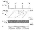
- FIG. 5is a timing chart illustrating an operation sequence of the integration circuit 30 .
- Section (a)illustrates the clock signal Vrst for turning on the reset switch 31
- Section (b)illustrates a voltage of the node B
- Section (c)illustrates an output from the AD converter 24
- Section (d)illustrates whether a finger is in touch with the touch panel 100 .
- the clock signals Vrstare output at times T 0 , T 1 , T 2 , and T 3 .
- a fingeris not in touch between the times T 0 and T 1 , in touch between the times T 1 and T 2 , and not in touch between the times T 2 and T 3 .
- a voltage of the node A( FIG. 4 ) is determined based on time when the current source I is charged to, for example, a terminal capacity Cp of the X electrode XP during nontouching of a finger, and based on time when the current source I is charged to a terminal capacity Cp of the X electrode XP and a capacity Cf during touching of a finger.
- a voltage of the node B( FIG. 4 ) becomes equal to a ground level when the reset switch 31 is turned on by the clock signal Vrst.
- a voltage of the node B at the time T 2 when the finger touchesis denoted by V(T 2 ), and a voltage of the node B at the time T 1 when the finger does not touch is denoted by V(T 1 ).
- a difference between the voltagesis indicated by a signal component, and represented by the following expression (1).
- Cpdenotes a terminal capacity
- Cfdenotes a capacity during touching of a finger
- Idenotes a current value of the current source I
- Ccdenotes an integration capacity of the integration circuit 30 .
- a signalis determined based on a ratio of the terminal capacity Cp of the touch panel 100 to the capacity Cf during touching of the finger.
- the capacity Cpis reduced, or the capacity Cf is increased.
- the increase of the capacity Cfnecessitates enlargement of an electrode, which is a trade-off with coordinate detection resolution.
- reduction of the terminal capacity Cpis preferable, and sensitivities and an S/N ratio can be improved. Reducing an inter-terminal difference of the terminal capacity Cp enables improvement of sensitivity uniformity in a panel surface.
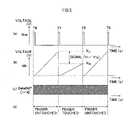
- FIG. 6is a graph illustrating a wiring line width as a parameter in a relationship between an inter-wiring line capacity CL and a wiring line interval S of the adjacent drawing wiring lines XW and YW.
- an abscissaindicates a wiring line interval S ( ⁇ m)
- an ordinateindicates an inter-wiring line capacity CL (pF/mm).
- the inter-wiring line capacity CLis reduced by increasing the wiring line interval S from 0 ⁇ m to 100 ⁇ m.
- the inter-wiring line capacity CLis increased by enlarging the wiring line widths to 1 ⁇ W, 2 ⁇ W, and 4 ⁇ W. From this graph, the inter-wiring line capacity CL is formulated, which is represented by the following expression (2).
- ⁇ 0denotes a vacuum dielectric constant
- ⁇ rdenotes a specific dielectric constant of the transparent substrate SUB.
- the inter-wiring line capacity CLdepends on a wiring line width W and a wiring line interval S. Presuming that a wiring line length L is constant, to reduce the inter-wiring line capacity CL, preferably, the wiring line interval S is set large, and the wiring line width W is set small.
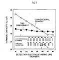
- FIG. 7is a graph illustrating terminal capacities Cp of adjacently arranged detection electrode wiring lines.
- an abscissaindicates detection electrode wiring lines (# 1 to # 8 ), and an ordinate indicates terminal capacities (pF) of the detection electrode wiring lines.
- the detection electrode wiring lines # 1 to # 8are larger in wiring line width W and wiring line intervals S with other adjacent detection electrode wiring lines are smaller in this order. In this case, though not illustrated in FIG. 7 , the detection electrode wiring lines # 1 to # 8 are shorter in length in this order. For comparison, corresponding to the detection electrode wiring lines, conventional detection electrode wiring lines are equal in wiring line width W and in wiring line interval S.
- the terminal capacity Cpis generated in the detection electrode wiring line, and a sum total of a detection electrode capacity C(PIX), an inter-wiring line capacity Cs, and a counter ground capacity Cg of a drawing wiring line.
- FIG. 7illustrates terminal capacities Cp of the conventional detection electrode wiring lines.
- the terminal capacities Cp of the conventional detection electrode wiring lines # 1 to # 8are smaller in this order. It is because the detection electrode wiring lines # 1 to # 8 are shorter in length in this order.
- the terminal capacities Cp of the detection electrode wiring lines # 1 to # 8are almost constant. In other words, a capacity difference among the detection electrode wiring lines can be reduced. It is because as described above, in each detection electrode wiring line, a wiring line width W and a wiring line interval S are optimally adjusted.
- FIG. 8is a schematic plan diagram illustrating an electrostatic capacitance type touch panel according to another embodiment of the present invention, and corresponding to FIG. 1 .
- a difference in configuration from FIG. 1is that the number of X electrodes XP is, for example, four which is smaller than that of Y electrodes YP.
- An FPC terminalis disposed almost directly below an electrode forming area TT.
- the present inventionis applied to the drawing wiring lines YW from the Y electrodes YP, but not applied to any drawing wiring lines XW from the X electrodes XP.
- the drawing wiring lines YW from the Y electrodes YPare drawing wiring lines YW (Line (A)), YW (Line (B)), YW (Line (C)), . . . in order of nearness to the FPC terminal.
- Line widthsare set smaller in order of the drawing wiring lines YW (Line (A)), YW (Line (B)), YW (Line (C)), . . . .
- Wiring line intervalsare larger between the drawing wiring lines YW (Line (A)) and YW (Line (B)), between the drawing wiring lines YW (Line (B)) and YW (Line (C)), between the drawing wiring lines YW (Line (C)) and YW (Line (D)), . . . in this order.
- FIG. 9is a schematic plan diagram illustrating an electrostatic capacitance type touch panel according to another embodiment of the present invention, and corresponding to FIG. 8 .
- a difference in configuration from FIG. 8is that drawing wiring lines YW from Y electrodes YP to an FPC terminal are drawn from both sides (left and right of FIG. 9 ) of an electrode forming area TT.
- FIG. 10is a schematic plan diagram illustrating an electrostatic capacitance type touch panel according to another embodiment of the present invention, and corresponding to FIG. 9 .
- drawing wiring lines YW from Y electrodes YP to an FPC terminalare all drawn from both sides (left and right of FIG. 10 ) of an electrode forming area TT.
- drawing wiring lines XW from X electrodes XP to the FPC terminalare all drawn from both sides (upper and lower sides of FIG. 10 ) of forming areas of the X and Y electrodes XP and YP.
- the present inventionis applied only to the drawing wiring lines YW from the Y electrodes YP. It is because the drawing wiring lines XW from the X electrodes XP are almost equal in length.
- FIG. 11is a schematic plan diagram illustrating an electrostatic capacitance type touch panel according to another embodiment of the present invention, and corresponding to FIG. 8 .
- an electrode forming area TTis long in an X direction but short in a Y direction.
- four Y electrodes YPare disposed in parallel, and six X electrodes XP are disposed in parallel.
- An FPC terminalis disposed in a lower right side of FIG. 11 with respect to forming areas of the X and Y electrodes XP and YP.
- drawing wiring lines XW from the X electrodes XP to the FPC terminalare different in length
- drawing wiring lines YW from the Y electrodes YP to the FPC terminalare different in length.
- the present inventionis applied to the drawing wiring lines XW from the X electrodes XP and the drawing wiring lines YW from the Y electrodes YP.
- FIG. 12is an exploded perspective diagram illustrating a display device which includes the touch panel 100 described above according to an embodiment of the present invention.
- a liquid crystal display deviceis used for the display device.
- a TFT substrate SUB 1 and a counter substrate SUB 2 sandwiching a liquid crystal LCconstitute a liquid crystal display panel PNL.
- a plurality of pixels arranged in matrixare formed, and independently driven by thin-film transistors (not shown) formed adjacently to the pixels.
- a flexible substrate FPCis connected to the TFT substrate SUB 1 , and a signal is supplied to each pixel via the flexible substrate FPC.
- a lower polarizing plate POL 1is disposed on a surface of the TFT substrate SUB 1 opposite to the liquid crystal LC
- an upper polarizing plate POL 2is disposed on a surface of the counter substrate SUB 2 opposite to the liquid crystal LC, whereby behavior of the liquid crystal LC of each pixel can be made visible.
- Each pixel of the liquid crystal display panel PNLincludes an element for controlling a light transmission amount, and a backlight BL is disposed on a surface of the liquid crystal display panel PNL opposite to an observer.
- the touch panel 100is disposed on a surface of the liquid crystal display panel PNL on the observer side, and a display area of the liquid crystal display panel PNL can be viewed through the touch panel 100 .
- X and Y electrodes XP and YPare formed on a main surface of the transparent substrate SUB, and an acrylic plate PB is disposed on the surface thereof to protect the X and Y electrodes XP and YP.
- the touch panel 100is bonded to the liquid crystal display panel via an adhesive layer ADL.
- FIG. 13is an exploded perspective diagram illustrating a display device which includes the touch panel 100 according to another embodiment of the present invention, and corresponding to FIG. 12 .
- a difference in configuration from FIG. 12is that X and Y electrodes XP and YP of the touch panel 100 are formed on a surface of a transparent substrate SUB on a liquid crystal display panel side.
- the touch panel 100is bonded to the liquid crystal display panel via an adhesive layer ADL on the surface where the X and Y electrodes XP and YP have been formed.
- This configurationenables the transparent substrate SUB also to protect the X and Y electrodes XP and YP.
- the touch panel 100itself can be thinned.
- FIG. 14illustrates a system configuration when a display device includes the touch panel 100 to be configured as a so-called screen input image display device.
- the screen input image display deviceincludes a liquid crystal display module LDM and a mobile device main body MM.
- the liquid crystal display module LDMincludes the touch panel 100 including a touch panel controller 100 A, and a liquid crystal display panel PNL including a liquid crystal display driver DR.
- the mobile device main body MMincludes a processor CPU. Communication between the processor CPU and the touch panel controller 100 A is carried out via SPI or I2C, and communication between the processor CPU and the liquid crystal display driver DR is carried out via an RGB interface or a CPU interface.
- initial setting datasuch as a start, a sampling frequency or detection resolution is transmitted from the mobile device main body MM to the liquid crystal display module LDM.
- Detection data(X and Y coordinate data or presence/absence of finger touching) is transmitted from the liquid crystal display module LDM to the mobile device main body MM, and processed by the processor CPU of the mobile device main body MM based on position information detected by the touch panel 100 to be added to display information of the liquid crystal display panel.
- FIG. 15illustrates, for example, an appearance of a mobile electronic device which includes the electrostatic capacitance type touch panel 100 of the present invention.
- the mobile electronic deviceincludes a display area AR of a liquid crystal display device, and the electrostatic capacitance type touch panel 100 stacked on this display area AR.
- the electrostatic capacitance type touch panel 100stacked on this display area AR.
- an iconis displayed in the display area AR visible through the electrostatic capacitance type touch panel 100 .
- liquid crystal display deviceas the exemplary display device.
- other display devicessuch as an organic EL display device may be used.
Landscapes
- Engineering & Computer Science (AREA)
- General Engineering & Computer Science (AREA)
- Theoretical Computer Science (AREA)
- Human Computer Interaction (AREA)
- Physics & Mathematics (AREA)
- General Physics & Mathematics (AREA)
- Position Input By Displaying (AREA)
- Switches That Are Operated By Magnetic Or Electric Fields (AREA)
- Push-Button Switches (AREA)
Abstract
Description
- The present application claims priority from Japanese application JP 2008-106350 filed on Apr. 16, 2008, the content of which is hereby incorporated by reference into this application.
- 1. Field of the Invention
- The present invention relates to an electrostatic capacitance type touch panel and a screen input display device including the same.
- 2. Description of the Related Art
- The electrostatic capacitance type touch panel stacked in a display area of the screen input display device includes X electrodes disposed in parallel in a Y direction to extend in an X direction and Y electrodes disposed in parallel in the X direction to extend in the Y direction which are formed on a substrate via an insulating film.
- When touching the electrostatic capacitance type touch panel by a finger, based on a capacity change of an electrode of this portion, for example, an external circuit calculates X and Y coordinates of a contact point of the finger to reflect information thereof in the display device.
- U.S. Pat. No. 5,844,506 discloses such a technology.
- The electrostatic capacitance type touch panel includes a connection terminal disposed in a part of a periphery on the substrate, and the X and Y electrodes are drawn to the connection terminal by drawing wiring lines.
- In this case, for example, the drawing wiring lines connected to the X and Y electrodes are different in length, causing a great difference in capacity between the drawing wiring lines themselves and other adjacent drawing wiring lines.
- Thus, in the electrostatic capacitance type touch panel configured to obtain a detection output based on a capacity difference of the electrodes at the time of finger nontouching and touching, a difference occurs in detection sensitivities, blocking improvement of detection accuracy.
- As countermeasures, a circuit may be disposed to correct the capacity difference between the drawing wiring lines. However, the circuit is disadvantageously enlarged.
- It is an object of the present invention to provide an electrostatic capacitance type touch panel capable of improving detection accuracy by making detection sensitivities uniform without increasing a circuit size.
- It is another object of the present invention to provide a screen input display device which includes a touch panel of high detection accuracy to achieve high speed without increasing a circuit size.
- Representative aspects of the present invention disclosed herein are briefly outlined below.
- (1) According to Item (1) of the present invention, there is provided an electrostatic capacitance type touch panel, comprising:
- a substrate;
- a plurality of first electrodes disposed in parallel on the substrate;
- an insulating film formed so as to cover the plurality of first electrodes;
- a plurality of second electrodes disposed in parallel to intersect the plurality of first electrodes on the insulating film;
- a plurality of first drawing wiring lines connected to the plurality of first electrodes to be drawn to a connection terminal; and
- a plurality of second drawing wiring lines connected to the plurality of second electrodes to be drawn to the connection terminal,
- wherein the plurality of first or second drawing wiring lines have different lengths, larger widths as the lengths are shorter, and larger intervals between adjacent two of the plurality of first or second drawing wiring lines as the lengths are longer.
- (2) According to Item (2) of the present invention, in the electrostatic capacitance type touch panel of the invention according to Item (1), each of the plurality of first electrodes and the plurality of second electrodes is formed so that pad portions and thin line portions thinner than the pad portions are alternately arrayed in an extending direction of the each of the plurality of first electrodes and the plurality of second electrodes, and in plan view, the pad portions of the plurality of first electrodes and the pad portions of the plurality of second electrodes are arranged so as not to overlap each other.
- (3) According to Item (3) of the present invention, in the electrostatic capacitance type touch panel of the invention according to Item (1), the plurality of first electrodes comprise a transparent conductive layer;
- the plurality of first drawing wiring lines are formed into a two-layer structure including a transparent conductive layer and a metal layer;
- the plurality of second electrodes comprise a transparent conductive layer; and
- the plurality of second drawing wiring lines are formed into a two-layer structure including a transparent conductive layer and a metal layer.
- (4) According to Item (4) of the present invention, there is provided an electrostatic capacitance type touch panel, comprising:
- a substrate;
- a plurality of first electrodes disposed in parallel on the substrate;
- an insulating film formed so as to cover the plurality of first electrodes;
- a plurality of second electrodes disposed in parallel to intersect the plurality of first electrodes on the insulating film;
- a plurality of first drawing wiring lines connected to the plurality of first electrodes to be drawn to a connection terminal; and
- a plurality of second drawing wiring lines connected to the plurality of second electrodes to be drawn to the connection terminal, wherein:
- the plurality of first drawing wiring lines have different lengths, larger widths as the lengths are shorter, and larger intervals between adjacent two of the plurality of first drawing wiring lines as the lengths are longer; and
- the plurality of second drawing wiring lines have different lengths, larger widths as the lengths are shorter, and larger intervals between adjacent two of the plurality of second drawing wiring lines as the lengths are longer.
- (5) According to Item (5) of the present invention, in the electrostatic capacitance type touch panel of the invention according to Item (4), each of the plurality of first electrodes and the plurality of second electrodes is formed so that pad portions and thin line portions thinner than the pad portions are alternately arrayed in an extending direction of the each of the plurality of first electrodes and the plurality of second electrodes, and in plan view, the pad portions of the plurality of first electrodes and the pad portions of the plurality of second electrodes are arranged so as not to overlap each other.
- (6) According to Item (6) of the present invention, in the electrostatic capacitance type touch panel of the invention according to Item (4), the plurality of first electrodes comprise a transparent conductive layer;
- the plurality of first drawing wiring lines are formed into a two-layer structure including a transparent conductive layer and a metal layer;
- the plurality of second electrodes comprise a transparent conductive layer; and
- the plurality of second drawing wiring lines are formed into a two-layer structure including a transparent conductive layer and a metal layer.
- (7) According item (7) of the present invention, there is provided a screen input display device, comprising:
- a display device; and
- an electrostatic capacitance type touch panel disposed in at least a display area of the display device, wherein:
- the electrostatic capacitance type touch panel comprises:
- a substrate;
- a plurality of first electrodes disposed in parallel on the substrate;
- an insulating film formed so as to cover the plurality of first electrodes;
- a plurality of second electrodes disposed in parallel to intersect the plurality of first electrodes on the insulating film;
- a plurality of first drawing wiring lines connected to the plurality of first electrodes to be drawn to a connection terminal; and
- a plurality of second drawing wiring lines connected to the plurality of second electrodes to be drawn to the connection terminal, wherein
- the plurality of first or second drawing wiring lines have different lengths, larger widths as the lengths are shorter, and larger intervals between adjacent two of the plurality of first or second drawing wiring lines as the lengths are longer.
- (8) According to Item (8) of the present invention, in the screen input display device of the invention according to Item (7), each of the plurality of first electrodes and the plurality of second electrodes is formed so that pad portions and thin line portions thinner than the pad portions are alternately arrayed in an extending direction of the each of the plurality of first electrodes and the plurality of second electrodes, and in plan view, the pad portions of the plurality of first electrodes and the pad portions of the plurality of second electrodes are arranged so as not to overlap each other.
- (9) According to Item (9) of the present invention, in the screen input display device of the invention according to Item (7), the plurality of first electrodes comprise a transparent conductive layer;
- the plurality of first drawing wiring lines are formed into a two-layer structure including a transparent conductive layer and a metal layer;
- the plurality of second electrodes comprise a transparent conductive layer; and
- the plurality of second drawing wiring lines are formed into a two-layer structure including a transparent conductive layer and a metal layer.
- (10) According to Item 10 of the present invention, there is provided a screen input display device, comprising:
- a display device; and
- an electrostatic capacitance type touch panel disposed in at least a display area of the display device, wherein:
- the electrostatic capacitance type touch panel comprises:
- a substrate;
- a plurality of first electrodes disposed in parallel on the substrate;
- an insulating film formed so as to cover the plurality of first electrodes;
- a plurality of second electrodes disposed in parallel to intersect the plurality of first electrodes on the insulating film;
- a plurality of first drawing wiring lines connected to the plurality of first electrodes to be drawn to a connection terminal; and
- a plurality of second drawing wiring lines connected to the plurality of second electrodes to be drawn to the connection terminal, wherein
- the plurality of first drawing wiring lines have different lengths, larger widths as the lengths are shorter, and larger intervals between adjacent two of the plurality of first drawing wiring lines as the lengths are longer; and
- the plurality of second drawing wiring lines have different lengths, larger widths as the lengths are shorter, and larger intervals between adjacent two of the plurality of second drawing wiring lines as the lengths are longer.
- (11) According to Item (11) of the present invention, in the screen input display device of the invention according to Item (10), each of the plurality of first electrodes and the plurality of second electrodes is formed so that pad portions and thin line portions thinner than the pad portions are alternately arrayed in an extending direction of the each of the plurality of first electrodes and the plurality of second electrodes, and in plan view, the pad portions of the plurality of first electrodes and the pad portions of the plurality of second electrodes are arranged so as not to overlap each other.
- (12) According to Item (12) of the present invention, in the screen input display device of the invention according to Item (10), the plurality of first electrodes comprise a transparent conductive layer;
- the plurality of first drawing wiring lines are formed into a two-layer structure including a transparent conductive layer and a metal layer;
- the plurality of second electrodes comprise a transparent conductive layer; and
- the plurality of second drawing wiring lines are formed into a two-layer structure including a transparent conductive layer and a metal layer.
- The present invention is not limited to those structures. Various changes can be made without departing from technical ideas of the present invention. Other components of the present invention become apparent upon reading the detailed description of the present invention in conjunction with the drawings.
- The electrostatic capacitance type touch panel of the present invention improves detection accuracy by making detection sensitivities uniform.
- The screen input display device of the present invention includes the touch panel of high detection accuracy and achieves high speed.
- Other effects of the present invention become apparent upon reading the detailed description of the present invention.
- In the accompanying drawings:
FIG. 1 is a plan diagram illustrating an electrostatic capacitance type touch panel according to an embodiment of the present invention;FIG. 2 is an enlarged diagram of a portion in a broken-line frame ofFIG. 1 ;FIG. 3A is a sectional diagram cut on a line IIIA-IIIA ofFIG. 1 ;FIG. 3B is a sectional diagram cut on a line IIIB-IIIB ofFIG. 1 ;FIG. 3C is a sectional diagram cut on a line IIIC-IIIC ofFIG. 1 ;FIG. 3D is a sectional diagram cut on a line IIID-IIID ofFIG. 1 ;FIG. 4 is a circuit diagram illustrating a controller connected to the electrostatic capacitance type touch panel according to an embodiment of the present invention;FIG. 5 illustrates signal detection of the electrostatic capacitance type touch panel;FIG. 6 is a graph illustrating effects of the present invention;FIG. 7 is a graph illustrating effects of the present invention;FIG. 8 is a plan diagram illustrating an electrostatic capacitance type touch panel according to another embodiment of the present invention;FIG. 9 is a plan diagram illustrating an electrostatic capacitance type touch panel according to still another embodiment of the present invention;FIG. 10 is a plan diagram illustrating an electrostatic capacitance type touch panel according to a further embodiment of the present invention;FIG. 11 is a plan diagram illustrating an electrostatic capacitance type touch panel according to a further embodiment of the present invention;FIG. 12 is an exploded perspective diagram illustrating a display device including an electrostatic capacitance type touch panel according to an embodiment of the present invention;FIG. 13 is an exploded perspective diagram illustrating a display device including an electrostatic capacitance type touch panel according to another embodiment of the present invention;FIG. 14 illustrates a system configuration of a screen input image display device including a touch panel; andFIG. 15 illustrates an appearance of a mobile device to which the present invention is applied.- Preferred embodiments of the present invention are described with reference to the drawings. In the drawings and the embodiments, identical or similar components are denoted by similar reference numerals, and description thereof is omitted.
FIG. 1 is a schematic plan diagram illustrating an electrostatic capacitance type touch panel according to a first embodiment of the present invention.FIG. 3A is a sectional diagram cut on a line IIIA-IIIA ofFIG. 1 ,FIG. 3B is a sectional diagram cut on a line IIIB-IIIB,FIG. 3C is a sectional diagram cut on a line IIIC-IIIC, andFIG. 3D is a sectional diagram cut on a line IIID-IIID,- The electrostatic capacitance type touch panel (
touch panel 100 hereinafter) is formed by sequentially laminating, for example, on a main surface of a transparent substrate SUB made of glass, (e.g., six) Y electrodes YP disposed in parallel in an Y direction to extend in a X direction ofFIG. 1 , an insulating film IN (refer toFIGS. 3A to 3D ) formed to cover the Y electrodes YP, and (e.g., six) X electrodes XP disposed in parallel in the X direction to extend in the Y direction ofFIG. 1 . - The Y electrode YP is formed by a transparent conductive film of, for example, indium tin oxide (ITO). The Y electrode YP is formed into a pattern where wide portions (may be referred to as pad portions) and narrow portions (may be referred to as linear portions) are alternately arrayed in the extending direction. The other Y electrodes YP arranged in parallel have similar patterns. In each Y electrode YP, the pad portion and the linear portion are arranged in the X direction of
FIG. 1 . For example, the pad portion is formed into a diamond shape connected to the linear portion at a pair of opposing corners. - The X electrode XP is similarly formed by a transparent conductive film of, for example, indium tin oxide (ITO). The X electrode XP is formed into a pattern where wide portions (may be referred to as pad portions) and narrow portions (may be referred to as linear portions) are alternately arrayed in the extending direction. The other X electrodes XP arranged in parallel have similar patterns. In each X electrode XP, the pad portion and the linear portion are arranged in the Y direction of
FIG. 1 . For example, the pad portion is formed into a diamond shape connected to the linear portion at a pair of opposing corners. - In plan view, for example, the X and Y electrodes XP and YP intersect each other at the linear portions, and the pad portions of the X and Y electrodes XP and YP are formed not to overlap each other. In other words, the Y electrode YP is formed to surround a diamond area by four adjacent pad portions. In the diamond area, the pad portion of the X electrode XP is disposed to have spaces with the four pads of the Y electrode YP. Thus, the pad portions of the X and Y electrodes XP and YP are arranged in a staggered manner on a center of the transparent substrate SUB excluding its periphery.
- The area where the X and Y electrodes XP and YP are formed as described above may be referred to as an electrode forming area TT below.
- Each Y electrode YP is connected to a drawing wiring line YW extending in the X direction of
FIG. 1 in, for example, an end of the right side ofFIG. 1 . The drawing wiring line YW is bent in the Y direction ofFIG. 1 , and then connected to a connection terminal CNT disposed on, for example, a lower right side of the transparent substrate SUB illustrated inFIG. 1 . Each X electrode XP is connected to a drawing wiring line XW extending in the Y direction ofFIG. 1 in, for example, an end of the lower side ofFIG. 1 . The drawing wiring line XW is bent in the X direction ofFIG. 1 and then connected to the connection terminal CNT. - On the transparent substrate SUB, the drawing wiring lines YW and XW respectively connected to the Y electrode YP and the X electrode XP, and the connection terminal CNT are formed in an area outside the electrode forming area TT. The area outside the electrode forming area TT on the transparent substrate SUB may be referred to as a frame below.
FIG. 2 is an enlarged diagram illustrating a portion in a broken-line frame ofFIG. 1 .FIG. 2 illustrates a part of each drawing wiring line XW for guiding the X electrode XP to the connection terminal CNT. Because of positioning of the connection terminal CNT on the right side ofFIG. 2 with respect to the electrode forming area TT, among the drawing wiring lines XW illustrated inFIG. 2 , the drawing wiring line XW (Line (A)) positioned on the right side is shortest, and the drawing wiring lines XW (Line (B)), XW (Line (C)), XW (Line (D)), . . . arranged on the left side are gradually longer in this order. In this case, a relationship of Wa>Wb>Wc>Wd> . . . is established, where Wa to Wd respectively denote widths of the drawing wiring lines XW (Line (A)), XW (Line (B)), XW (Line (C)), and XW (Line (D)). A relationship of Sa<Sb<Sc< . . . is established, where Sa to Sc respectively denote intervals between the drawing wiring lines XW (Line (A)) and XW (Line (B)), between the drawing wiring lines XW (Line (B)) and XW (Line (C)), and between the drawing wiring lines XW (Line (C)) and XW (Line (D)).- The width of the drawing wiring line XW can be reduced to a level which causes no problem with wiring line resistance in driving of the
touch panel 100, and the wiring line interval can be reduced to a level permitted by a frame space of thetouch panel 100. Thus, a wiring line width and a wiring line interval can be set according to design values of wiring line resistance and a frame space. - Configuring the drawing wiring line XW in this manner enables reductions of an inter-wiring line capacity CL and a ground capacity CG of long drawing wiring lines, and a capacity difference (difference in terminal capacity Cp) between the X electrode XP and the drawing wiring line XW (may be referred to as a detection electrode wiring line hereinafter) as described below.
FIG. 2 is the enlarged diagram of the portion in the broken-line frame ofFIG. 1 , illustrating a configuration of the drawing wiring line XW connected to the X electrode XP. As can be seen inFIG. 1 , a similar configuration is employed for the drawing wiring line YW connected to the Y electrode YP. In other words, widths of the drawing wiring lines YW are sequentially smaller and intervals between adjacent drawing wiring lines YW are sequentially larger, as lengths thereof are longer.- As illustrated in
FIG. 2 , each drawing wiring line YW is formed into a two-layer structure including a transparent conductive layer ITO made of ITO and a metal layer MT made of aluminum or chrome. In other words, the transparent conductive layer ITO is formed as an extending portion of the Y electrode YP, and the metal layer MT is laminated on the extending portion. In this way, connection between the Y electrode YP and the drawing wiring line YW can be reliable, and electrical resistance can be reduced. FIG. 4 is a circuit diagram illustrating an embodiment of a configuration of acontroller 3 when thetouch panel 100 is connected to thecontroller 3.- In
FIG. 4 , thecontroller 3 includes anintegration circuit 30 connected to thetouch panel 100, anAD converter 24 connected to theintegration circuit 30, and anarithmetic processing circuit 25 connected to theAD converter 24. - The
integration circuit 30 is configured by connecting an integration capacity (Cc)33 and areset switch 31 to an I/O terminal of anoperational amplifier 32 in parallel. An input terminal of theoperational amplifier 32 is a node A connected to, for example, the X electrode XP of thetouch panel 100, and a current source I is connected to the node A. Charges generated at a terminal capacity Cp of thetouch panel 100 and a finger touch capacity Cf are stored in the integration capacity (Cc)33. An output voltage of an output terminal (node B) of theoperational amplifier 32 is determined based on a ratio of the integration capacity (Cc)33 to (Cp+Cf). The integration capacity (Cc)33 accordingly becomes a parameter to determine sensitivities. - The
reset switch 31 is controlled based on a clock signal Vrst turned on/off at a predetermined period, and detection time is controlled. - An output from the
integration circuit 30 is digitized via theAD converter 24, and then thearithmetic processing circuit 25 calculates X and Y coordinates of a finger which has touched thetouch panel 100. - In this configuration, a circuit for conversion into time may be applied to an AD conversion unit in place of the
AD converter 24. The configuration of thecontroller 3 is only exemplary. Any configuration can be employed as long as a change in capacity or charges can be detected. FIG. 5 is a timing chart illustrating an operation sequence of theintegration circuit 30. Section (a) illustrates the clock signal Vrst for turning on thereset switch 31, Section (b) illustrates a voltage of the node B, Section (c) illustrates an output from theAD converter 24, and Section (d) illustrates whether a finger is in touch with thetouch panel 100. InFIG. 5 , the clock signals Vrst are output at times T0, T1, T2, and T3. A finger is not in touch between the times T0 and T1, in touch between the times T1 and T2, and not in touch between the times T2 and T3.- A voltage of the node A (
FIG. 4 ) is determined based on time when the current source I is charged to, for example, a terminal capacity Cp of the X electrode XP during nontouching of a finger, and based on time when the current source I is charged to a terminal capacity Cp of the X electrode XP and a capacity Cf during touching of a finger. A voltage of the node B (FIG. 4 ) becomes equal to a ground level when thereset switch 31 is turned on by the clock signal Vrst. - A voltage of the node B at the time T2 when the finger touches is denoted by V(T2), and a voltage of the node B at the time T1 when the finger does not touch is denoted by V(T1).
- A difference between the voltages is indicated by a signal component, and represented by the following expression (1).
V(T2)−V(T1)=ItCc/Cp−ItCc/(Cf+Cp)=Cf/Cp/(Cf+Cp)Cc (1)- where Cp denotes a terminal capacity, Cf denotes a capacity during touching of a finger, I denotes a current value of the current source I, and Cc denotes an integration capacity of the
integration circuit 30. - As apparent from the expression (1), a signal is determined based on a ratio of the terminal capacity Cp of the
touch panel 100 to the capacity Cf during touching of the finger. To improve sensitivities, the capacity Cp is reduced, or the capacity Cf is increased. The increase of the capacity Cf necessitates enlargement of an electrode, which is a trade-off with coordinate detection resolution. Thus, reduction of the terminal capacity Cp is preferable, and sensitivities and an S/N ratio can be improved. Reducing an inter-terminal difference of the terminal capacity Cp enables improvement of sensitivity uniformity in a panel surface. FIG. 6 is a graph illustrating a wiring line width as a parameter in a relationship between an inter-wiring line capacity CL and a wiring line interval S of the adjacent drawing wiring lines XW and YW. In the graph, an abscissa indicates a wiring line interval S (μm), and an ordinate indicates an inter-wiring line capacity CL (pF/mm). As apparent fromFIG. 6 , the inter-wiring line capacity CL is reduced by increasing the wiring line interval S from 0 μm to 100 μm. The inter-wiring line capacity CL is increased by enlarging the wiring line widths to 1×W, 2×W, and 4×W. From this graph, the inter-wiring line capacity CL is formulated, which is represented by the following expression (2).
CL=ε0εrW0.13S−0.13L (2)- where ε0denotes a vacuum dielectric constant, and εrdenotes a specific dielectric constant of the transparent substrate SUB.
- As can be understood from the expression (2), the inter-wiring line capacity CL depends on a wiring line width W and a wiring line interval S. Presuming that a wiring line length L is constant, to reduce the inter-wiring line capacity CL, preferably, the wiring line interval S is set large, and the wiring line width W is set small.
FIG. 7 is a graph illustrating terminal capacities Cp of adjacently arranged detection electrode wiring lines. In the graph, an abscissa indicates detection electrode wiring lines (#1 to #8), and an ordinate indicates terminal capacities (pF) of the detection electrode wiring lines.- As illustrated in a solid-line frame α of
FIG. 7 , the detection electrodewiring lines # 1 to #8 are larger in wiring line width W and wiring line intervals S with other adjacent detection electrode wiring lines are smaller in this order. In this case, though not illustrated inFIG. 7 , the detection electrodewiring lines # 1 to #8 are shorter in length in this order. For comparison, corresponding to the detection electrode wiring lines, conventional detection electrode wiring lines are equal in wiring line width W and in wiring line interval S. - The terminal capacity Cp is generated in the detection electrode wiring line, and a sum total of a detection electrode capacity C(PIX), an inter-wiring line capacity Cs, and a counter ground capacity Cg of a drawing wiring line.
FIG. 7 illustrates terminal capacities Cp of the conventional detection electrode wiring lines. The terminal capacities Cp of the conventional detection electrodewiring lines # 1 to #8 are smaller in this order. It is because the detection electrodewiring lines # 1 to #8 are shorter in length in this order.- On the other hand, in the configuration of the detection electrode wiring lines of this embodiment, the terminal capacities Cp of the detection electrode
wiring lines # 1 to #8 are almost constant. In other words, a capacity difference among the detection electrode wiring lines can be reduced. It is because as described above, in each detection electrode wiring line, a wiring line width W and a wiring line interval S are optimally adjusted. FIG. 8 is a schematic plan diagram illustrating an electrostatic capacitance type touch panel according to another embodiment of the present invention, and corresponding toFIG. 1 .- A difference in configuration from
FIG. 1 is that the number of X electrodes XP is, for example, four which is smaller than that of Y electrodes YP. An FPC terminal is disposed almost directly below an electrode forming area TT. Thus, there is no big difference in length among drawing wiring lines XW from the X electrodes XP to the FPC terminal while there is a big difference in length among drawing wiring lines YW from the Y electrodes YP to the FPC terminal. - Thus, the present invention is applied to the drawing wiring lines YW from the Y electrodes YP, but not applied to any drawing wiring lines XW from the X electrodes XP. In other words, as illustrated in
FIG. 8 , the drawing wiring lines YW from the Y electrodes YP are drawing wiring lines YW (Line (A)), YW (Line (B)), YW (Line (C)), . . . in order of nearness to the FPC terminal. Line widths are set smaller in order of the drawing wiring lines YW (Line (A)), YW (Line (B)), YW (Line (C)), . . . . Wiring line intervals are larger between the drawing wiring lines YW (Line (A)) and YW (Line (B)), between the drawing wiring lines YW (Line (B)) and YW (Line (C)), between the drawing wiring lines YW (Line (C)) and YW (Line (D)), . . . in this order. FIG. 9 is a schematic plan diagram illustrating an electrostatic capacitance type touch panel according to another embodiment of the present invention, and corresponding toFIG. 8 .- A difference in configuration from
FIG. 8 is that drawing wiring lines YW from Y electrodes YP to an FPC terminal are drawn from both sides (left and right ofFIG. 9 ) of an electrode forming area TT. - In other words, from the left side of the electrode forming area TT of
FIG. 9 , odd-number drawing wiring lines YW counted from the FPC terminal side are drawn to be guided to the FPC terminal. From the right side of the electrode forming area TT ofFIG. 9 , even-number drawing wiring lines YW counted from the FPC terminal side are drawn to be guided to the FPC terminal. - In this case, as described above, according to lengths of the drawing wiring lines YW, wiring line widths are set, and wiring line intervals with the other adjacent drawing wiring lines YW are set. Thus, when the drawing wiring lines are drawn from both sides of the forming areas of the X and Y electrodes XP and YP, the wiring line widths and the wiring line intervals of the drawing wiring lines can be increased by effectively utilizing a frame space. When there is a margin in the inter-wiring line capacity CL, the frame space can be reduced.
FIG. 10 is a schematic plan diagram illustrating an electrostatic capacitance type touch panel according to another embodiment of the present invention, and corresponding toFIG. 9 .- A difference in configuration from
FIG. 9 is that drawing wiring lines YW from Y electrodes YP to an FPC terminal are all drawn from both sides (left and right ofFIG. 10 ) of an electrode forming area TT. InFIG. 10 , drawing wiring lines XW from X electrodes XP to the FPC terminal are all drawn from both sides (upper and lower sides ofFIG. 10 ) of forming areas of the X and Y electrodes XP and YP. - In this case, for example, the present invention is applied only to the drawing wiring lines YW from the Y electrodes YP. It is because the drawing wiring lines XW from the X electrodes XP are almost equal in length.
- As described above, for each Y electrode YP, signals are supplied from both ends thereof via the drawing wiring line YW. Thus, a driving load of the
controller 3 can be ideally halved, preventing a problem of higher resistance caused by thinning of the X and Y electrodes XP and YP. Formation of the drawing wiring lines YW from both sides of the Y electrode YP inevitably leads to an increase of the inter-wiring line capacity CL. Thus, application of the present invention contributes to reduction of the inter-wiring line capacity CL. FIG. 11 is a schematic plan diagram illustrating an electrostatic capacitance type touch panel according to another embodiment of the present invention, and corresponding toFIG. 8 .- A difference in configuration from
FIG. 8 is that an electrode forming area TT is long in an X direction but short in a Y direction. For example, four Y electrodes YP are disposed in parallel, and six X electrodes XP are disposed in parallel. - An FPC terminal is disposed in a lower right side of
FIG. 11 with respect to forming areas of the X and Y electrodes XP and YP. - In this case, drawing wiring lines XW from the X electrodes XP to the FPC terminal are different in length, and drawing wiring lines YW from the Y electrodes YP to the FPC terminal are different in length. Thus, the present invention is applied to the drawing wiring lines XW from the X electrodes XP and the drawing wiring lines YW from the Y electrodes YP.
FIG. 12 is an exploded perspective diagram illustrating a display device which includes thetouch panel 100 described above according to an embodiment of the present invention.- For example, a liquid crystal display device is used for the display device. In the liquid crystal display device, a TFT substrate SUB1 and a counter substrate SUB2 sandwiching a liquid crystal LC constitute a liquid crystal display panel PNL. On a surface of the TFT substrate SUB1 on the liquid crystal LC side, a plurality of pixels arranged in matrix are formed, and independently driven by thin-film transistors (not shown) formed adjacently to the pixels. A flexible substrate FPC is connected to the TFT substrate SUB1, and a signal is supplied to each pixel via the flexible substrate FPC. A lower polarizing plate POL1 is disposed on a surface of the TFT substrate SUB1 opposite to the liquid crystal LC, and an upper polarizing plate POL2 is disposed on a surface of the counter substrate SUB2 opposite to the liquid crystal LC, whereby behavior of the liquid crystal LC of each pixel can be made visible.
- Each pixel of the liquid crystal display panel PNL includes an element for controlling a light transmission amount, and a backlight BL is disposed on a surface of the liquid crystal display panel PNL opposite to an observer.
- The
touch panel 100 is disposed on a surface of the liquid crystal display panel PNL on the observer side, and a display area of the liquid crystal display panel PNL can be viewed through thetouch panel 100. In thetouch panel 100, X and Y electrodes XP and YP are formed on a main surface of the transparent substrate SUB, and an acrylic plate PB is disposed on the surface thereof to protect the X and Y electrodes XP and YP. Thetouch panel 100 is bonded to the liquid crystal display panel via an adhesive layer ADL. FIG. 13 is an exploded perspective diagram illustrating a display device which includes thetouch panel 100 according to another embodiment of the present invention, and corresponding toFIG. 12 .- A difference in configuration from
FIG. 12 is that X and Y electrodes XP and YP of thetouch panel 100 are formed on a surface of a transparent substrate SUB on a liquid crystal display panel side. Thetouch panel 100 is bonded to the liquid crystal display panel via an adhesive layer ADL on the surface where the X and Y electrodes XP and YP have been formed. This configuration enables the transparent substrate SUB also to protect the X and Y electrodes XP and YP. Thus, thetouch panel 100 itself can be thinned. FIG. 14 illustrates a system configuration when a display device includes thetouch panel 100 to be configured as a so-called screen input image display device.- For example, the screen input image display device includes a liquid crystal display module LDM and a mobile device main body MM. The liquid crystal display module LDM includes the
touch panel 100 including atouch panel controller 100A, and a liquid crystal display panel PNL including a liquid crystal display driver DR. - The mobile device main body MM includes a processor CPU. Communication between the processor CPU and the
touch panel controller 100A is carried out via SPI or I2C, and communication between the processor CPU and the liquid crystal display driver DR is carried out via an RGB interface or a CPU interface. - Thus, initial setting data such as a start, a sampling frequency or detection resolution is transmitted from the mobile device main body MM to the liquid crystal display module LDM. Detection data (X and Y coordinate data or presence/absence of finger touching) is transmitted from the liquid crystal display module LDM to the mobile device main body MM, and processed by the processor CPU of the mobile device main body MM based on position information detected by the
touch panel 100 to be added to display information of the liquid crystal display panel. FIG. 15 illustrates, for example, an appearance of a mobile electronic device which includes the electrostatic capacitancetype touch panel 100 of the present invention.- For example, the mobile electronic device includes a display area AR of a liquid crystal display device, and the electrostatic capacitance
type touch panel 100 stacked on this display area AR. For example, an icon is displayed in the display area AR visible through the electrostatic capacitancetype touch panel 100. By finger-touching a portion of the electrostatic capacitancetype touch panel 100 on the icon, information can be reflected in the liquid crystal display device. - The embodiments described above have been directed to the liquid crystal display device as the exemplary display device. However, other display devices such as an organic EL display device may be used.
- The present invention has been described by way of the embodiments. However, the configurations of the embodiments described above are only examples, and various changes can appropriately be made without departing from the technical ideas of the present invention. The configurations of the embodiments described above may be combined as long as they are not contradictory to one another.
- While there have been described what are at present considered to be certain embodiments of the invention, it is understood that various modifications may be made thereto, and it is intended that the appended claims cover all such modifications as fall within the true spirit and scope of the invention.
Claims (12)
Applications Claiming Priority (2)
| Application Number | Priority Date | Filing Date | Title |
|---|---|---|---|
| JP2008106350AJP5103254B2 (en) | 2008-04-16 | 2008-04-16 | Capacitive touch panel and screen input type display device including the same |
| JP2008-106350 | 2008-04-16 |
Publications (2)
| Publication Number | Publication Date |
|---|---|
| US20090262095A1true US20090262095A1 (en) | 2009-10-22 |
| US8638313B2 US8638313B2 (en) | 2014-01-28 |
Family
ID=41200744
Family Applications (1)
| Application Number | Title | Priority Date | Filing Date |
|---|---|---|---|
| US12/423,858Active2032-03-29US8638313B2 (en) | 2008-04-16 | 2009-04-15 | Electrostatic capacitance type touch panel and screen input display device including the same |
Country Status (3)
| Country | Link |
|---|---|
| US (1) | US8638313B2 (en) |
| JP (1) | JP5103254B2 (en) |
| CN (1) | CN101561737B (en) |
Cited By (32)
| Publication number | Priority date | Publication date | Assignee | Title |
|---|---|---|---|---|
| US20110018826A1 (en)* | 2009-07-24 | 2011-01-27 | Sony Corporation | Electrostatic capacitance type input apparatus and display apparatus with input function including the same |
| US20110210937A1 (en)* | 2010-02-26 | 2011-09-01 | Samsung Electronics Co., Ltd. | Foldable touch screen display apparatus |
| US20110267286A1 (en)* | 2010-04-28 | 2011-11-03 | DerLead Investment Ltd. | Touch panel |
| CN102741790A (en)* | 2010-09-22 | 2012-10-17 | 日本写真印刷株式会社 | Multi-touch panel comprising equipotential line distortion compensator unit |
| US20120313871A1 (en)* | 2011-06-07 | 2012-12-13 | Novatek Microelectronics Corp. | Touch panel and display apparatus |
| CN102830863A (en)* | 2011-06-16 | 2012-12-19 | 联咏科技股份有限公司 | Touch panel and display device |
| CN102830845A (en)* | 2012-08-21 | 2012-12-19 | 深圳市立德通讯器材有限公司 | Production method of touch display screen |
| WO2012168548A3 (en)* | 2011-06-07 | 2013-01-31 | Nokia Corporation | Method and apparatus for touch panel |
| CN103076913A (en)* | 2010-07-22 | 2013-05-01 | 阿尔卑斯电气株式会社 | Input device and method of manufacturing the same |
| US20130278538A1 (en)* | 2012-04-19 | 2013-10-24 | Samuel Brunet | Self-Capacitance Measurement |
| US20140335350A1 (en)* | 2011-12-05 | 2014-11-13 | Hitachi Chemical Company, Ltd. | Method for forming protective film on electrode for touch panel, photosensitive resin composition and photosensitive element, and method for manufacturing touch panel |
| US20150227235A1 (en)* | 2014-02-10 | 2015-08-13 | Samsung Display Co., Ltd. | Touch panels and methods of manufacturing touch panels |
| US9189033B2 (en) | 2010-09-29 | 2015-11-17 | Dai Nippon Printing Co., Ltd. | Touchscreen panel sensor film and manufacturing method thereof |
| US9207273B2 (en) | 2013-01-14 | 2015-12-08 | Samsung Display Co., Ltd. | Apparatus for inspecting touch panel and method thereof |
| US20160147335A1 (en)* | 2013-04-12 | 2016-05-26 | Shin-Etsu Polymer Co., Ltd. | Sheet for manufacturing sensor sheet, method for manufacturing sheet for manufacturing sensor sheet, sensor sheet for touch pad, and method for manufacturing sensor sheet for touch pad |
| US20160328036A1 (en)* | 2015-05-06 | 2016-11-10 | Lg Electronics Inc. | Touch panel and display device including the same |
| US9513749B2 (en) | 2013-03-11 | 2016-12-06 | Japan Display Inc. | Touch-sensor device, display device, and electronic device |
| EP3073358A4 (en)* | 2013-11-22 | 2017-06-21 | Toppan Printing Co., Ltd. | Transparent conductive layered product, touch panel, and display device |
| US9882561B2 (en) | 2012-06-12 | 2018-01-30 | Fujikura Ltd. | Input device |
| US20180136760A1 (en)* | 2015-10-05 | 2018-05-17 | G2Touch Co., Ltd | Touch screen panel |
| US20180182822A1 (en)* | 2016-12-26 | 2018-06-28 | Samsung Display Co., Ltd. | Touch sensor and display device including the same |
| EP3410271A1 (en)* | 2017-06-01 | 2018-12-05 | LG Display Co., Ltd. | Touch display device |
| US10191587B2 (en)* | 2008-07-31 | 2019-01-29 | Japan Display Inc. | Touch panel |
| US10386719B2 (en) | 2011-12-05 | 2019-08-20 | Hitachi Chemical Company, Ltd. | Method for forming resin cured film pattern, photosensitive resin composition, photosensitive element, method for producing touch panel, and resin cured film |
| TWI685783B (en)* | 2018-05-03 | 2020-02-21 | 奕力科技股份有限公司 | Touch panel with narrow border |
| US10782838B2 (en) | 2018-05-03 | 2020-09-22 | Ili Technology Corp. | Mutual capacitive touch panel with narrow border having transparent winding segments |
| US10818698B2 (en)* | 2016-06-09 | 2020-10-27 | Sharp Kabushiki Kaisha | Active matrix substrate and display device and touch panel display device including same |
| US10886340B2 (en)* | 2019-05-28 | 2021-01-05 | Wuhan Tianma Micro-Electronics Co., Ltd. | Display panel and display device with reduced frame width |
| US11054951B2 (en) | 2019-09-30 | 2021-07-06 | Seiko Epson Corporation | Display device with electrostatic capacitive touch panel |
| US11182016B2 (en) | 2017-10-03 | 2021-11-23 | Wacom Co., Ltd. | Sensor panel for detecting stylus signal sent from stylus |
| US11301092B2 (en) | 2019-09-30 | 2022-04-12 | Seiko Epson Corporation | Display device with electrostatic capacitive touch panel |
| US20250053272A1 (en)* | 2022-05-31 | 2025-02-13 | Boe Technology Group Co., Ltd. | Touch display panel, method for manufacturing the same, and display apparatus |
Families Citing this family (44)
| Publication number | Priority date | Publication date | Assignee | Title |
|---|---|---|---|---|
| US9069418B2 (en)* | 2008-06-06 | 2015-06-30 | Apple Inc. | High resistivity metal fan out |
| JP2010108222A (en)* | 2008-10-30 | 2010-05-13 | Kyocera Corp | Touch panel and touch panel type display device |
| JP4958020B2 (en)* | 2009-03-31 | 2012-06-20 | 大日本印刷株式会社 | Touch panel sensor, laminate for manufacturing touch panel sensor, and method for manufacturing touch panel sensor |
| KR200457891Y1 (en)* | 2009-08-25 | 2012-01-06 | 민리드 엘티디. | Matrix touch panel |
| JP2011100357A (en)* | 2009-11-06 | 2011-05-19 | Hosiden Corp | Touch panel and manufacturing method therefor |
| JP2012014669A (en)* | 2009-11-20 | 2012-01-19 | Fujifilm Corp | Conductive sheet, method of using conductive sheet and electrostatic capacitive touch panel |
| JP2011128674A (en)* | 2009-12-15 | 2011-06-30 | Sony Corp | Electrostatic capacitance-type input device and method for manufacturing the same |
| KR101474897B1 (en)* | 2009-12-28 | 2014-12-19 | 쿄세라 코포레이션 | Input device and display device provided with same |
| JP5121814B2 (en)* | 2009-12-28 | 2013-01-16 | 三菱電機株式会社 | Touch panel and display device |
| WO2011102168A1 (en)* | 2010-02-17 | 2011-08-25 | 日本写真印刷株式会社 | Transparent electrode film |
| TWI471798B (en)* | 2010-03-12 | 2015-02-01 | Alps Electric Co Ltd | Input device |
| CN102200867B (en)* | 2010-03-24 | 2016-03-30 | 上海天马微电子有限公司 | capacitive touch sensing device |
| CN102200866B (en)* | 2010-03-24 | 2015-11-25 | 上海天马微电子有限公司 | Mutual capacitance touch sensing device, detection method thereof and touch display device |
| JP5637492B2 (en)* | 2010-03-26 | 2014-12-10 | 株式会社デンソー | Capacitive touch panel device |
| CN101882021A (en)* | 2010-06-08 | 2010-11-10 | 苏州瀚瑞微电子有限公司 | Touch pad layout method |
| KR101113524B1 (en)* | 2010-07-27 | 2012-02-29 | 삼성모바일디스플레이주식회사 | Touch Screen Panel Device |
| CN103392198B (en)* | 2011-02-28 | 2015-11-25 | 夏普株式会社 | Electrode substrate and display device and touch panel having same |
| TW201237720A (en)* | 2011-03-11 | 2012-09-16 | Cando Corp | Thin type flexible capacitive touch device |
| KR101812606B1 (en) | 2011-04-26 | 2017-12-27 | 니폰 메크트론 가부시키가이샤 | Method for manufacturing transparent printed circuit and method for manufacturing transparent touch panel |
| JP5822395B2 (en)* | 2012-01-25 | 2015-11-24 | 富士フイルム株式会社 | Conductive sheet, inspection method and manufacturing method thereof |
| JP2013225266A (en)* | 2012-04-23 | 2013-10-31 | Fujitsu Component Ltd | Touch panel |
| CN103425307A (en)* | 2012-05-18 | 2013-12-04 | 榕增光电科技有限公司 | Sensing circuit structure of touch panel |
| US20140043278A1 (en)* | 2012-08-09 | 2014-02-13 | 3M Innovative Properties Company | Electrode configuration for large touch screen |
| JP2014102747A (en)* | 2012-11-21 | 2014-06-05 | Panasonic Liquid Crystal Display Co Ltd | Touch panel device and control method of touch panel device |
| CN103677414B (en)* | 2013-12-09 | 2016-10-05 | 合肥京东方光电科技有限公司 | A kind of touch display unit |
| KR102199613B1 (en)* | 2014-01-08 | 2021-01-07 | 삼성전자주식회사 | Touch panel and manufacturing method thereof |
| JP2015141555A (en)* | 2014-01-29 | 2015-08-03 | シナプティクス・ディスプレイ・デバイス合同会社 | Detection circuit and semiconductor integrated circuit including the same |
| US20160139708A1 (en)* | 2014-11-13 | 2016-05-19 | Industrial Technology Research Institute | Touch panel |
| KR101931897B1 (en)* | 2015-01-16 | 2018-12-21 | 알프스 덴키 가부시키가이샤 | Capacitive sensor |
| JP6562706B2 (en)* | 2015-05-13 | 2019-08-21 | 三菱電機株式会社 | Surface device, touch screen and liquid crystal display device |
| TWI611328B (en)* | 2015-06-22 | 2018-01-11 | 友達光電股份有限公司 | Touch display panel |
| JP6498578B2 (en)* | 2015-09-28 | 2019-04-10 | 日本航空電子工業株式会社 | Touch panel |
| JP6539190B2 (en)* | 2015-11-20 | 2019-07-03 | 株式会社ジャパンディスプレイ | Touch detection device and display device with touch detection function |
| CN106066740B (en) | 2016-08-02 | 2019-02-12 | 厦门天马微电子有限公司 | Touch-control display panel and touch control display apparatus |
| CN106055171B (en)* | 2016-08-08 | 2019-02-12 | 京东方科技集团股份有限公司 | An array substrate and its manufacturing method and display device |
| CN110554811A (en)* | 2018-05-30 | 2019-12-10 | 奕力科技股份有限公司 | Touch panel with narrow frame |
| CN110557887B (en)* | 2018-05-31 | 2021-10-12 | 京东方科技集团股份有限公司 | Circuit alignment assembly and display device |
| JP6613512B1 (en) | 2018-08-31 | 2019-12-04 | レノボ・シンガポール・プライベート・リミテッド | Electronics |
| KR102427303B1 (en) | 2018-09-10 | 2022-08-01 | 삼성디스플레이 주식회사 | Display device |
| KR102611671B1 (en) | 2018-09-19 | 2023-12-08 | 삼성디스플레이 주식회사 | Touch sensing unit and display apparatus having the same |
| CN110032302B (en)* | 2019-03-21 | 2022-09-13 | 深圳曦华科技有限公司 | Touch detection method |
| JPWO2021024735A1 (en)* | 2019-08-07 | 2021-02-11 | ||
| JP7331160B2 (en)* | 2020-09-02 | 2023-08-22 | 株式会社ジャパンディスプレイ | Display device |
| CN112612375B (en)* | 2020-12-30 | 2023-08-08 | 安徽鸿程光电有限公司 | Touch panel, touch display and manufacturing method of touch display |
Citations (9)
| Publication number | Priority date | Publication date | Assignee | Title |
|---|---|---|---|---|
| US5473195A (en)* | 1993-04-13 | 1995-12-05 | Nec Corporation | Semiconductor integrated circuit device having parallel signal wirings variable in either width or interval |
| US5650597A (en)* | 1995-01-20 | 1997-07-22 | Dynapro Systems, Inc. | Capacitive touch sensor |
| US5844506A (en)* | 1994-04-05 | 1998-12-01 | Binstead; Ronald Peter | Multiple input proximity detector and touchpad system |
| US6549193B1 (en)* | 1998-10-09 | 2003-04-15 | 3M Innovative Properties Company | Touch panel with improved linear response and minimal border width electrode pattern |
| US20040174356A1 (en)* | 2003-03-06 | 2004-09-09 | Pioneer Corporation | Apparatus for driving display panel |
| US7030860B1 (en)* | 1999-10-08 | 2006-04-18 | Synaptics Incorporated | Flexible transparent touch sensing system for electronic devices |
| US20090002338A1 (en)* | 2007-06-27 | 2009-01-01 | Masayoshi Kinoshita | Screen input type image display |
| US20090244021A1 (en)* | 2008-03-26 | 2009-10-01 | Epson Imaging Devices Corporation | Electrical capacitance input device, display apparatus with input function and electronic apparatus |
| US8040321B2 (en)* | 2006-07-10 | 2011-10-18 | Cypress Semiconductor Corporation | Touch-sensor with shared capacitive sensors |
- 2008
- 2008-04-16JPJP2008106350Apatent/JP5103254B2/ennot_activeExpired - Fee Related
- 2009
- 2009-04-15USUS12/423,858patent/US8638313B2/enactiveActive
- 2009-04-16CNCN2009101335938Apatent/CN101561737B/enactiveActive
Patent Citations (9)
| Publication number | Priority date | Publication date | Assignee | Title |
|---|---|---|---|---|
| US5473195A (en)* | 1993-04-13 | 1995-12-05 | Nec Corporation | Semiconductor integrated circuit device having parallel signal wirings variable in either width or interval |
| US5844506A (en)* | 1994-04-05 | 1998-12-01 | Binstead; Ronald Peter | Multiple input proximity detector and touchpad system |
| US5650597A (en)* | 1995-01-20 | 1997-07-22 | Dynapro Systems, Inc. | Capacitive touch sensor |
| US6549193B1 (en)* | 1998-10-09 | 2003-04-15 | 3M Innovative Properties Company | Touch panel with improved linear response and minimal border width electrode pattern |
| US7030860B1 (en)* | 1999-10-08 | 2006-04-18 | Synaptics Incorporated | Flexible transparent touch sensing system for electronic devices |
| US20040174356A1 (en)* | 2003-03-06 | 2004-09-09 | Pioneer Corporation | Apparatus for driving display panel |
| US8040321B2 (en)* | 2006-07-10 | 2011-10-18 | Cypress Semiconductor Corporation | Touch-sensor with shared capacitive sensors |
| US20090002338A1 (en)* | 2007-06-27 | 2009-01-01 | Masayoshi Kinoshita | Screen input type image display |
| US20090244021A1 (en)* | 2008-03-26 | 2009-10-01 | Epson Imaging Devices Corporation | Electrical capacitance input device, display apparatus with input function and electronic apparatus |
Cited By (54)
| Publication number | Priority date | Publication date | Assignee | Title |
|---|---|---|---|---|
| US10191587B2 (en)* | 2008-07-31 | 2019-01-29 | Japan Display Inc. | Touch panel |
| US10423275B2 (en) | 2008-07-31 | 2019-09-24 | Japan Display Inc. | Touch panel |
| US10599262B2 (en) | 2008-07-31 | 2020-03-24 | Japan Display Inc. | Touch panel |
| US10908730B2 (en)* | 2008-07-31 | 2021-02-02 | Japan Display Inc. | Touch panel |
| US20110018826A1 (en)* | 2009-07-24 | 2011-01-27 | Sony Corporation | Electrostatic capacitance type input apparatus and display apparatus with input function including the same |
| US20110210937A1 (en)* | 2010-02-26 | 2011-09-01 | Samsung Electronics Co., Ltd. | Foldable touch screen display apparatus |
| US20110267286A1 (en)* | 2010-04-28 | 2011-11-03 | DerLead Investment Ltd. | Touch panel |
| CN103076913A (en)* | 2010-07-22 | 2013-05-01 | 阿尔卑斯电气株式会社 | Input device and method of manufacturing the same |
| US8658919B2 (en) | 2010-09-22 | 2014-02-25 | Nissha Printing Co., Ltd. | Multi-touch panel including equipotential line distortion corrector |
| CN102741790A (en)* | 2010-09-22 | 2012-10-17 | 日本写真印刷株式会社 | Multi-touch panel comprising equipotential line distortion compensator unit |
| US9189033B2 (en) | 2010-09-29 | 2015-11-17 | Dai Nippon Printing Co., Ltd. | Touchscreen panel sensor film and manufacturing method thereof |
| US9335842B2 (en)* | 2011-06-07 | 2016-05-10 | Novatek Microelectronics Corp. | Touch panel and display apparatus |
| WO2012168548A3 (en)* | 2011-06-07 | 2013-01-31 | Nokia Corporation | Method and apparatus for touch panel |
| US8823659B2 (en) | 2011-06-07 | 2014-09-02 | Nokia Corporation | Method and apparatus for touch panel |
| US20120313871A1 (en)* | 2011-06-07 | 2012-12-13 | Novatek Microelectronics Corp. | Touch panel and display apparatus |
| CN102830863A (en)* | 2011-06-16 | 2012-12-19 | 联咏科技股份有限公司 | Touch panel and display device |
| US20140335350A1 (en)* | 2011-12-05 | 2014-11-13 | Hitachi Chemical Company, Ltd. | Method for forming protective film on electrode for touch panel, photosensitive resin composition and photosensitive element, and method for manufacturing touch panel |
| US10663861B2 (en)* | 2011-12-05 | 2020-05-26 | Hitachi Chemical Company, Ltd. | Method for forming resin cured film pattern, photosensitive resin composition, photosensitive element, method for producing touch panel, and resin cured film |
| US10386719B2 (en) | 2011-12-05 | 2019-08-20 | Hitachi Chemical Company, Ltd. | Method for forming resin cured film pattern, photosensitive resin composition, photosensitive element, method for producing touch panel, and resin cured film |
| US9372582B2 (en)* | 2012-04-19 | 2016-06-21 | Atmel Corporation | Self-capacitance measurement |
| US20130278538A1 (en)* | 2012-04-19 | 2013-10-24 | Samuel Brunet | Self-Capacitance Measurement |
| US9882561B2 (en) | 2012-06-12 | 2018-01-30 | Fujikura Ltd. | Input device |
| CN102830845A (en)* | 2012-08-21 | 2012-12-19 | 深圳市立德通讯器材有限公司 | Production method of touch display screen |
| US9207273B2 (en) | 2013-01-14 | 2015-12-08 | Samsung Display Co., Ltd. | Apparatus for inspecting touch panel and method thereof |
| US9513749B2 (en) | 2013-03-11 | 2016-12-06 | Japan Display Inc. | Touch-sensor device, display device, and electronic device |
| US10185434B2 (en) | 2013-03-11 | 2019-01-22 | Japan Display Inc. | Display device |
| US20160147335A1 (en)* | 2013-04-12 | 2016-05-26 | Shin-Etsu Polymer Co., Ltd. | Sheet for manufacturing sensor sheet, method for manufacturing sheet for manufacturing sensor sheet, sensor sheet for touch pad, and method for manufacturing sensor sheet for touch pad |
| US10133399B2 (en) | 2013-11-22 | 2018-11-20 | VTS-Touchsensor Co. Ltd. | Transparent conductive laminate, touch panel and display device |
| EP3073358A4 (en)* | 2013-11-22 | 2017-06-21 | Toppan Printing Co., Ltd. | Transparent conductive layered product, touch panel, and display device |
| US10042487B2 (en)* | 2014-02-10 | 2018-08-07 | Samsung Display Co., Ltd. | Touch panels and methods of manufacturing touch panels |
| KR20150094808A (en)* | 2014-02-10 | 2015-08-20 | 삼성디스플레이 주식회사 | Touch panels and method of manufacturing a touch panel |
| KR102188985B1 (en)* | 2014-02-10 | 2020-12-10 | 삼성디스플레이 주식회사 | Touch panels and method of manufacturing a touch panel |
| US20150227235A1 (en)* | 2014-02-10 | 2015-08-13 | Samsung Display Co., Ltd. | Touch panels and methods of manufacturing touch panels |
| EP3091425B1 (en)* | 2015-05-06 | 2023-11-29 | Lg Chem, Ltd. | Touch panel and display device including the same |
| US9971432B2 (en)* | 2015-05-06 | 2018-05-15 | Lg Electronics Inc. | Touch panel having electrodes with different resistance and display device including the same |
| US20160328036A1 (en)* | 2015-05-06 | 2016-11-10 | Lg Electronics Inc. | Touch panel and display device including the same |
| US20180136760A1 (en)* | 2015-10-05 | 2018-05-17 | G2Touch Co., Ltd | Touch screen panel |
| US10818698B2 (en)* | 2016-06-09 | 2020-10-27 | Sharp Kabushiki Kaisha | Active matrix substrate and display device and touch panel display device including same |
| US11861123B2 (en) | 2016-12-26 | 2024-01-02 | Samsung Display Co., Ltd. | Touch sensor and display device including the same |
| US11243647B2 (en)* | 2016-12-26 | 2022-02-08 | Samsung Display Co., Ltd. | Touch sensor and display device including the same |
| US12386470B2 (en) | 2016-12-26 | 2025-08-12 | Samsung Display Co., Ltd. | Touch sensor and display device including the same |
| US20180182822A1 (en)* | 2016-12-26 | 2018-06-28 | Samsung Display Co., Ltd. | Touch sensor and display device including the same |
| EP3410271A1 (en)* | 2017-06-01 | 2018-12-05 | LG Display Co., Ltd. | Touch display device |
| US10551979B2 (en) | 2017-06-01 | 2020-02-04 | Lg Display Co., Ltd. | Touch display device |
| US11507223B2 (en) | 2017-10-03 | 2022-11-22 | Wacom Co., Ltd. | Sensor panel for detecting stylus signal sent from stylus |
| US11182016B2 (en) | 2017-10-03 | 2021-11-23 | Wacom Co., Ltd. | Sensor panel for detecting stylus signal sent from stylus |
| US11977701B2 (en) | 2017-10-03 | 2024-05-07 | Wacom Co., Ltd. | Sensor panel for detecting stylus signal sent from stylus |
| US12393299B2 (en) | 2017-10-03 | 2025-08-19 | Wacom Co., Ltd. | Sensor panel for detecting stylus signal sent from stylus |
| US10782838B2 (en) | 2018-05-03 | 2020-09-22 | Ili Technology Corp. | Mutual capacitive touch panel with narrow border having transparent winding segments |
| TWI685783B (en)* | 2018-05-03 | 2020-02-21 | 奕力科技股份有限公司 | Touch panel with narrow border |
| US10886340B2 (en)* | 2019-05-28 | 2021-01-05 | Wuhan Tianma Micro-Electronics Co., Ltd. | Display panel and display device with reduced frame width |
| US11054951B2 (en) | 2019-09-30 | 2021-07-06 | Seiko Epson Corporation | Display device with electrostatic capacitive touch panel |
| US11301092B2 (en) | 2019-09-30 | 2022-04-12 | Seiko Epson Corporation | Display device with electrostatic capacitive touch panel |
| US20250053272A1 (en)* | 2022-05-31 | 2025-02-13 | Boe Technology Group Co., Ltd. | Touch display panel, method for manufacturing the same, and display apparatus |
Also Published As
| Publication number | Publication date |
|---|---|
| US8638313B2 (en) | 2014-01-28 |
| JP5103254B2 (en) | 2012-12-19 |
| JP2009258935A (en) | 2009-11-05 |
| CN101561737B (en) | 2011-05-25 |
| CN101561737A (en) | 2009-10-21 |
Similar Documents
| Publication | Publication Date | Title |
|---|---|---|
| US8638313B2 (en) | Electrostatic capacitance type touch panel and screen input display device including the same | |
| US10474287B2 (en) | Double-sided touch-sensitive panel with shield and drive combined layer | |
| US7924350B2 (en) | Capacitance type touch panel | |
| TWI390283B (en) | Touch panel | |
| US8284169B2 (en) | Display device | |
| KR101542043B1 (en) | Touch screen panel | |
| US20180275809A1 (en) | In-cell touch screen and display device | |
| CN1326031C (en) | Signal line of touch panel display device and forming method thereof | |
| US20150029148A1 (en) | Capacitive in-cell touch screen panel and display device | |
| EP2818992A2 (en) | Touch-control display device with integration of capacitive and electromagnetic touch units | |
| US20150268762A1 (en) | In-cell touch panel and display device | |
| US20190243493A1 (en) | Touch panel, method of driving touch panel, and touch device | |
| CN100590581C (en) | Touch panel and portable electronic device with same | |
| KR20110137988A (en) | Display with touch sensing | |
| US20110096019A1 (en) | Touch panel and touch display device | |
| CN102890379B (en) | Pixel unit and thin film transistor liquid crystal display (TFT-LCD) | |
| US10120502B2 (en) | Array substrate, touch display panel and display apparatus containing the same, and method for driving the touch display panel | |
| US20180046295A1 (en) | Touch display device | |
| CN101819494B (en) | Image display system | |
| US11829540B2 (en) | Array substrate and touch display device | |
| KR20140093445A (en) | Self capacitor type in-cell touch liquid crystal display device | |
| US11099693B2 (en) | Touch-sensing display substrate, touch-sensing display apparatus, method of operating touch-sensing display apparatus, and method of fabricating touch-sensing display substrate | |
| WO2013179598A1 (en) | Embedded touch screen | |
| CN114564127B (en) | Touch panel and display device | |
| KR20130024328A (en) | Electrostatic capacity type touch screen panel |
Legal Events
| Date | Code | Title | Description |
|---|---|---|---|
| AS | Assignment | Owner name:HITACHI DISPLAYS, LTD., JAPAN Free format text:ASSIGNMENT OF ASSIGNORS INTEREST;ASSIGNORS:KINOSHITA, MASAYOSHI;MAMBA, NORIO;HATANO, MUTSUKO;REEL/FRAME:022848/0245;SIGNING DATES FROM 20090421 TO 20090424 Owner name:HITACHI DISPLAYS, LTD., JAPAN Free format text:ASSIGNMENT OF ASSIGNORS INTEREST;ASSIGNORS:KINOSHITA, MASAYOSHI;MAMBA, NORIO;HATANO, MUTSUKO;SIGNING DATES FROM 20090421 TO 20090424;REEL/FRAME:022848/0245 | |
| AS | Assignment | Owner name:PANASONIC LIQUID CRYSTAL DISPLAY CO., LTD., JAPAN Free format text:MERGER;ASSIGNOR:IPS ALPHA SUPPORT CO., LTD.;REEL/FRAME:027093/0937 Effective date:20101001 Owner name:IPS ALPHA SUPPORT CO., LTD., JAPAN Free format text:COMPANY SPLIT PLAN TRANSFERRING FIFTY (50) PERCENT SHARE IN PATENT APPLICATIONS;ASSIGNOR:HITACHI DISPLAYS, LTD.;REEL/FRAME:027092/0684 Effective date:20100630 | |
| AS | Assignment | Owner name:JAPAN DISPLAY EAST, INC., JAPAN Free format text:CHANGE OF NAME;ASSIGNOR:HITACHI DISPLAYS, LTD.;REEL/FRAME:031765/0633 Effective date:20120401 | |
| AS | Assignment | Owner name:JAPAN DISPLAY INC., JAPAN Free format text:CHANGE OF NAME;ASSIGNOR:JAPAN DISPLAY EAST, INC.;REEL/FRAME:031806/0071 Effective date:20130401 | |
| STCF | Information on status: patent grant | Free format text:PATENTED CASE | |
| FPAY | Fee payment | Year of fee payment:4 | |
| MAFP | Maintenance fee payment | Free format text:PAYMENT OF MAINTENANCE FEE, 8TH YEAR, LARGE ENTITY (ORIGINAL EVENT CODE: M1552); ENTITY STATUS OF PATENT OWNER: LARGE ENTITY Year of fee payment:8 | |
| AS | Assignment | Owner name:PANASONIC INTELLECTUAL PROPERTY CORPORATION OF AMERICA, CALIFORNIA Free format text:NUNC PRO TUNC ASSIGNMENT;ASSIGNOR:PANASONIC LIQUID CRYSTAL DISPLAY CO., LTD.;REEL/FRAME:065615/0327 Effective date:20230828 | |
| AS | Assignment | Owner name:PANELTOUCH TECHNOLOGIES LLC, TEXAS Free format text:ASSIGNMENT OF ASSIGNORS INTEREST;ASSIGNORS:PANASONIC INTELLECTUAL PROPERTY CORPORATION OF AMERICA;JAPAN DISPLAY INC.;REEL/FRAME:067245/0560 Effective date:20240322 | |
| FEPP | Fee payment procedure | Free format text:MAINTENANCE FEE REMINDER MAILED (ORIGINAL EVENT CODE: REM.); ENTITY STATUS OF PATENT OWNER: LARGE ENTITY |