US20090261473A1 - Low fabrication cost, fine pitch and high reliability solder bump - Google Patents
Low fabrication cost, fine pitch and high reliability solder bumpDownload PDFInfo
- Publication number
- US20090261473A1 US20090261473A1US12/493,258US49325809AUS2009261473A1US 20090261473 A1US20090261473 A1US 20090261473A1US 49325809 AUS49325809 AUS 49325809AUS 2009261473 A1US2009261473 A1US 2009261473A1
- Authority
- US
- United States
- Prior art keywords
- layer
- chip
- over
- metal
- top surface
- Prior art date
- Legal status (The legal status is an assumption and is not a legal conclusion. Google has not performed a legal analysis and makes no representation as to the accuracy of the status listed.)
- Granted
Links
Images


Classifications
- H—ELECTRICITY
- H01—ELECTRIC ELEMENTS
- H01L—SEMICONDUCTOR DEVICES NOT COVERED BY CLASS H10
- H01L24/00—Arrangements for connecting or disconnecting semiconductor or solid-state bodies; Methods or apparatus related thereto
- H01L24/01—Means for bonding being attached to, or being formed on, the surface to be connected, e.g. chip-to-package, die-attach, "first-level" interconnects; Manufacturing methods related thereto
- H01L24/10—Bump connectors ; Manufacturing methods related thereto
- H01L24/11—Manufacturing methods
- H—ELECTRICITY
- H01—ELECTRIC ELEMENTS
- H01L—SEMICONDUCTOR DEVICES NOT COVERED BY CLASS H10
- H01L24/00—Arrangements for connecting or disconnecting semiconductor or solid-state bodies; Methods or apparatus related thereto
- H01L24/01—Means for bonding being attached to, or being formed on, the surface to be connected, e.g. chip-to-package, die-attach, "first-level" interconnects; Manufacturing methods related thereto
- H01L24/10—Bump connectors ; Manufacturing methods related thereto
- H01L24/12—Structure, shape, material or disposition of the bump connectors prior to the connecting process
- H01L24/13—Structure, shape, material or disposition of the bump connectors prior to the connecting process of an individual bump connector
- H—ELECTRICITY
- H01—ELECTRIC ELEMENTS
- H01L—SEMICONDUCTOR DEVICES NOT COVERED BY CLASS H10
- H01L25/00—Assemblies consisting of a plurality of semiconductor or other solid state devices
- H01L25/03—Assemblies consisting of a plurality of semiconductor or other solid state devices all the devices being of a type provided for in a single subclass of subclasses H10B, H10D, H10F, H10H, H10K or H10N, e.g. assemblies of rectifier diodes
- H01L25/04—Assemblies consisting of a plurality of semiconductor or other solid state devices all the devices being of a type provided for in a single subclass of subclasses H10B, H10D, H10F, H10H, H10K or H10N, e.g. assemblies of rectifier diodes the devices not having separate containers
- H01L25/065—Assemblies consisting of a plurality of semiconductor or other solid state devices all the devices being of a type provided for in a single subclass of subclasses H10B, H10D, H10F, H10H, H10K or H10N, e.g. assemblies of rectifier diodes the devices not having separate containers the devices being of a type provided for in group H10D89/00
- H01L25/0657—Stacked arrangements of devices
- H—ELECTRICITY
- H01—ELECTRIC ELEMENTS
- H01L—SEMICONDUCTOR DEVICES NOT COVERED BY CLASS H10
- H01L25/00—Assemblies consisting of a plurality of semiconductor or other solid state devices
- H01L25/50—Multistep manufacturing processes of assemblies consisting of devices, the devices being individual devices of subclass H10D or integrated devices of class H10
- H—ELECTRICITY
- H01—ELECTRIC ELEMENTS
- H01L—SEMICONDUCTOR DEVICES NOT COVERED BY CLASS H10
- H01L2224/00—Indexing scheme for arrangements for connecting or disconnecting semiconductor or solid-state bodies and methods related thereto as covered by H01L24/00
- H01L2224/01—Means for bonding being attached to, or being formed on, the surface to be connected, e.g. chip-to-package, die-attach, "first-level" interconnects; Manufacturing methods related thereto
- H01L2224/02—Bonding areas; Manufacturing methods related thereto
- H01L2224/03—Manufacturing methods
- H01L2224/036—Manufacturing methods by patterning a pre-deposited material
- H01L2224/0361—Physical or chemical etching
- H—ELECTRICITY
- H01—ELECTRIC ELEMENTS
- H01L—SEMICONDUCTOR DEVICES NOT COVERED BY CLASS H10
- H01L2224/00—Indexing scheme for arrangements for connecting or disconnecting semiconductor or solid-state bodies and methods related thereto as covered by H01L24/00
- H01L2224/01—Means for bonding being attached to, or being formed on, the surface to be connected, e.g. chip-to-package, die-attach, "first-level" interconnects; Manufacturing methods related thereto
- H01L2224/02—Bonding areas; Manufacturing methods related thereto
- H01L2224/03—Manufacturing methods
- H01L2224/039—Methods of manufacturing bonding areas involving a specific sequence of method steps
- H01L2224/03912—Methods of manufacturing bonding areas involving a specific sequence of method steps the bump being used as a mask for patterning the bonding area
- H—ELECTRICITY
- H01—ELECTRIC ELEMENTS
- H01L—SEMICONDUCTOR DEVICES NOT COVERED BY CLASS H10
- H01L2224/00—Indexing scheme for arrangements for connecting or disconnecting semiconductor or solid-state bodies and methods related thereto as covered by H01L24/00
- H01L2224/01—Means for bonding being attached to, or being formed on, the surface to be connected, e.g. chip-to-package, die-attach, "first-level" interconnects; Manufacturing methods related thereto
- H01L2224/02—Bonding areas; Manufacturing methods related thereto
- H01L2224/04—Structure, shape, material or disposition of the bonding areas prior to the connecting process
- H01L2224/0401—Bonding areas specifically adapted for bump connectors, e.g. under bump metallisation [UBM]
- H—ELECTRICITY
- H01—ELECTRIC ELEMENTS
- H01L—SEMICONDUCTOR DEVICES NOT COVERED BY CLASS H10
- H01L2224/00—Indexing scheme for arrangements for connecting or disconnecting semiconductor or solid-state bodies and methods related thereto as covered by H01L24/00
- H01L2224/01—Means for bonding being attached to, or being formed on, the surface to be connected, e.g. chip-to-package, die-attach, "first-level" interconnects; Manufacturing methods related thereto
- H01L2224/02—Bonding areas; Manufacturing methods related thereto
- H01L2224/04—Structure, shape, material or disposition of the bonding areas prior to the connecting process
- H01L2224/05—Structure, shape, material or disposition of the bonding areas prior to the connecting process of an individual bonding area
- H01L2224/05001—Internal layers
- H01L2224/0501—Shape
- H01L2224/05016—Shape in side view
- H01L2224/05018—Shape in side view being a conformal layer on a patterned surface
- H—ELECTRICITY
- H01—ELECTRIC ELEMENTS
- H01L—SEMICONDUCTOR DEVICES NOT COVERED BY CLASS H10
- H01L2224/00—Indexing scheme for arrangements for connecting or disconnecting semiconductor or solid-state bodies and methods related thereto as covered by H01L24/00
- H01L2224/01—Means for bonding being attached to, or being formed on, the surface to be connected, e.g. chip-to-package, die-attach, "first-level" interconnects; Manufacturing methods related thereto
- H01L2224/02—Bonding areas; Manufacturing methods related thereto
- H01L2224/04—Structure, shape, material or disposition of the bonding areas prior to the connecting process
- H01L2224/05—Structure, shape, material or disposition of the bonding areas prior to the connecting process of an individual bonding area
- H01L2224/0554—External layer
- H01L2224/0555—Shape
- H01L2224/05556—Shape in side view
- H01L2224/05558—Shape in side view conformal layer on a patterned surface
- H—ELECTRICITY
- H01—ELECTRIC ELEMENTS
- H01L—SEMICONDUCTOR DEVICES NOT COVERED BY CLASS H10
- H01L2224/00—Indexing scheme for arrangements for connecting or disconnecting semiconductor or solid-state bodies and methods related thereto as covered by H01L24/00
- H01L2224/01—Means for bonding being attached to, or being formed on, the surface to be connected, e.g. chip-to-package, die-attach, "first-level" interconnects; Manufacturing methods related thereto
- H01L2224/02—Bonding areas; Manufacturing methods related thereto
- H01L2224/04—Structure, shape, material or disposition of the bonding areas prior to the connecting process
- H01L2224/05—Structure, shape, material or disposition of the bonding areas prior to the connecting process of an individual bonding area
- H01L2224/0554—External layer
- H01L2224/0556—Disposition
- H01L2224/05571—Disposition the external layer being disposed in a recess of the surface
- H01L2224/05572—Disposition the external layer being disposed in a recess of the surface the external layer extending out of an opening
- H—ELECTRICITY
- H01—ELECTRIC ELEMENTS
- H01L—SEMICONDUCTOR DEVICES NOT COVERED BY CLASS H10
- H01L2224/00—Indexing scheme for arrangements for connecting or disconnecting semiconductor or solid-state bodies and methods related thereto as covered by H01L24/00
- H01L2224/01—Means for bonding being attached to, or being formed on, the surface to be connected, e.g. chip-to-package, die-attach, "first-level" interconnects; Manufacturing methods related thereto
- H01L2224/02—Bonding areas; Manufacturing methods related thereto
- H01L2224/04—Structure, shape, material or disposition of the bonding areas prior to the connecting process
- H01L2224/05—Structure, shape, material or disposition of the bonding areas prior to the connecting process of an individual bonding area
- H01L2224/0554—External layer
- H01L2224/05599—Material
- H01L2224/056—Material with a principal constituent of the material being a metal or a metalloid, e.g. boron [B], silicon [Si], germanium [Ge], arsenic [As], antimony [Sb], tellurium [Te] and polonium [Po], and alloys thereof
- H01L2224/05617—Material with a principal constituent of the material being a metal or a metalloid, e.g. boron [B], silicon [Si], germanium [Ge], arsenic [As], antimony [Sb], tellurium [Te] and polonium [Po], and alloys thereof the principal constituent melting at a temperature of greater than or equal to 400°C and less than 950°C
- H01L2224/05624—Aluminium [Al] as principal constituent
- H—ELECTRICITY
- H01—ELECTRIC ELEMENTS
- H01L—SEMICONDUCTOR DEVICES NOT COVERED BY CLASS H10
- H01L2224/00—Indexing scheme for arrangements for connecting or disconnecting semiconductor or solid-state bodies and methods related thereto as covered by H01L24/00
- H01L2224/01—Means for bonding being attached to, or being formed on, the surface to be connected, e.g. chip-to-package, die-attach, "first-level" interconnects; Manufacturing methods related thereto
- H01L2224/10—Bump connectors; Manufacturing methods related thereto
- H01L2224/11—Manufacturing methods
- H01L2224/114—Manufacturing methods by blanket deposition of the material of the bump connector
- H01L2224/1146—Plating
- H01L2224/11462—Electroplating
- H—ELECTRICITY
- H01—ELECTRIC ELEMENTS
- H01L—SEMICONDUCTOR DEVICES NOT COVERED BY CLASS H10
- H01L2224/00—Indexing scheme for arrangements for connecting or disconnecting semiconductor or solid-state bodies and methods related thereto as covered by H01L24/00
- H01L2224/01—Means for bonding being attached to, or being formed on, the surface to be connected, e.g. chip-to-package, die-attach, "first-level" interconnects; Manufacturing methods related thereto
- H01L2224/10—Bump connectors; Manufacturing methods related thereto
- H01L2224/11—Manufacturing methods
- H01L2224/1147—Manufacturing methods using a lift-off mask
- H—ELECTRICITY
- H01—ELECTRIC ELEMENTS
- H01L—SEMICONDUCTOR DEVICES NOT COVERED BY CLASS H10
- H01L2224/00—Indexing scheme for arrangements for connecting or disconnecting semiconductor or solid-state bodies and methods related thereto as covered by H01L24/00
- H01L2224/01—Means for bonding being attached to, or being formed on, the surface to be connected, e.g. chip-to-package, die-attach, "first-level" interconnects; Manufacturing methods related thereto
- H01L2224/10—Bump connectors; Manufacturing methods related thereto
- H01L2224/11—Manufacturing methods
- H01L2224/118—Post-treatment of the bump connector
- H01L2224/1183—Reworking, e.g. shaping
- H01L2224/11831—Reworking, e.g. shaping involving a chemical process, e.g. etching the bump connector
- H—ELECTRICITY
- H01—ELECTRIC ELEMENTS
- H01L—SEMICONDUCTOR DEVICES NOT COVERED BY CLASS H10
- H01L2224/00—Indexing scheme for arrangements for connecting or disconnecting semiconductor or solid-state bodies and methods related thereto as covered by H01L24/00
- H01L2224/01—Means for bonding being attached to, or being formed on, the surface to be connected, e.g. chip-to-package, die-attach, "first-level" interconnects; Manufacturing methods related thereto
- H01L2224/10—Bump connectors; Manufacturing methods related thereto
- H01L2224/11—Manufacturing methods
- H01L2224/118—Post-treatment of the bump connector
- H01L2224/11848—Thermal treatments, e.g. annealing, controlled cooling
- H01L2224/11849—Reflowing
- H—ELECTRICITY
- H01—ELECTRIC ELEMENTS
- H01L—SEMICONDUCTOR DEVICES NOT COVERED BY CLASS H10
- H01L2224/00—Indexing scheme for arrangements for connecting or disconnecting semiconductor or solid-state bodies and methods related thereto as covered by H01L24/00
- H01L2224/01—Means for bonding being attached to, or being formed on, the surface to be connected, e.g. chip-to-package, die-attach, "first-level" interconnects; Manufacturing methods related thereto
- H01L2224/10—Bump connectors; Manufacturing methods related thereto
- H01L2224/11—Manufacturing methods
- H01L2224/119—Methods of manufacturing bump connectors involving a specific sequence of method steps
- H01L2224/11901—Methods of manufacturing bump connectors involving a specific sequence of method steps with repetition of the same manufacturing step
- H—ELECTRICITY
- H01—ELECTRIC ELEMENTS
- H01L—SEMICONDUCTOR DEVICES NOT COVERED BY CLASS H10
- H01L2224/00—Indexing scheme for arrangements for connecting or disconnecting semiconductor or solid-state bodies and methods related thereto as covered by H01L24/00
- H01L2224/01—Means for bonding being attached to, or being formed on, the surface to be connected, e.g. chip-to-package, die-attach, "first-level" interconnects; Manufacturing methods related thereto
- H01L2224/10—Bump connectors; Manufacturing methods related thereto
- H01L2224/12—Structure, shape, material or disposition of the bump connectors prior to the connecting process
- H01L2224/13—Structure, shape, material or disposition of the bump connectors prior to the connecting process of an individual bump connector
- H01L2224/13001—Core members of the bump connector
- H01L2224/13005—Structure
- H01L2224/13007—Bump connector smaller than the underlying bonding area, e.g. than the under bump metallisation [UBM]
- H—ELECTRICITY
- H01—ELECTRIC ELEMENTS
- H01L—SEMICONDUCTOR DEVICES NOT COVERED BY CLASS H10
- H01L2224/00—Indexing scheme for arrangements for connecting or disconnecting semiconductor or solid-state bodies and methods related thereto as covered by H01L24/00
- H01L2224/01—Means for bonding being attached to, or being formed on, the surface to be connected, e.g. chip-to-package, die-attach, "first-level" interconnects; Manufacturing methods related thereto
- H01L2224/10—Bump connectors; Manufacturing methods related thereto
- H01L2224/12—Structure, shape, material or disposition of the bump connectors prior to the connecting process
- H01L2224/13—Structure, shape, material or disposition of the bump connectors prior to the connecting process of an individual bump connector
- H01L2224/13001—Core members of the bump connector
- H01L2224/1301—Shape
- H01L2224/13016—Shape in side view
- H01L2224/13017—Shape in side view being non uniform along the bump connector
- H—ELECTRICITY
- H01—ELECTRIC ELEMENTS
- H01L—SEMICONDUCTOR DEVICES NOT COVERED BY CLASS H10
- H01L2224/00—Indexing scheme for arrangements for connecting or disconnecting semiconductor or solid-state bodies and methods related thereto as covered by H01L24/00
- H01L2224/01—Means for bonding being attached to, or being formed on, the surface to be connected, e.g. chip-to-package, die-attach, "first-level" interconnects; Manufacturing methods related thereto
- H01L2224/10—Bump connectors; Manufacturing methods related thereto
- H01L2224/12—Structure, shape, material or disposition of the bump connectors prior to the connecting process
- H01L2224/13—Structure, shape, material or disposition of the bump connectors prior to the connecting process of an individual bump connector
- H01L2224/13001—Core members of the bump connector
- H01L2224/13075—Plural core members
- H01L2224/1308—Plural core members being stacked
- H01L2224/13083—Three-layer arrangements
- H—ELECTRICITY
- H01—ELECTRIC ELEMENTS
- H01L—SEMICONDUCTOR DEVICES NOT COVERED BY CLASS H10
- H01L2224/00—Indexing scheme for arrangements for connecting or disconnecting semiconductor or solid-state bodies and methods related thereto as covered by H01L24/00
- H01L2224/01—Means for bonding being attached to, or being formed on, the surface to be connected, e.g. chip-to-package, die-attach, "first-level" interconnects; Manufacturing methods related thereto
- H01L2224/10—Bump connectors; Manufacturing methods related thereto
- H01L2224/12—Structure, shape, material or disposition of the bump connectors prior to the connecting process
- H01L2224/13—Structure, shape, material or disposition of the bump connectors prior to the connecting process of an individual bump connector
- H01L2224/13001—Core members of the bump connector
- H01L2224/13099—Material
- H01L2224/131—Material with a principal constituent of the material being a metal or a metalloid, e.g. boron [B], silicon [Si], germanium [Ge], arsenic [As], antimony [Sb], tellurium [Te] and polonium [Po], and alloys thereof
- H01L2224/13138—Material with a principal constituent of the material being a metal or a metalloid, e.g. boron [B], silicon [Si], germanium [Ge], arsenic [As], antimony [Sb], tellurium [Te] and polonium [Po], and alloys thereof the principal constituent melting at a temperature of greater than or equal to 950°C and less than 1550°C
- H01L2224/13144—Gold [Au] as principal constituent
- H—ELECTRICITY
- H01—ELECTRIC ELEMENTS
- H01L—SEMICONDUCTOR DEVICES NOT COVERED BY CLASS H10
- H01L2224/00—Indexing scheme for arrangements for connecting or disconnecting semiconductor or solid-state bodies and methods related thereto as covered by H01L24/00
- H01L2224/01—Means for bonding being attached to, or being formed on, the surface to be connected, e.g. chip-to-package, die-attach, "first-level" interconnects; Manufacturing methods related thereto
- H01L2224/10—Bump connectors; Manufacturing methods related thereto
- H01L2224/12—Structure, shape, material or disposition of the bump connectors prior to the connecting process
- H01L2224/13—Structure, shape, material or disposition of the bump connectors prior to the connecting process of an individual bump connector
- H01L2224/13001—Core members of the bump connector
- H01L2224/13099—Material
- H01L2224/131—Material with a principal constituent of the material being a metal or a metalloid, e.g. boron [B], silicon [Si], germanium [Ge], arsenic [As], antimony [Sb], tellurium [Te] and polonium [Po], and alloys thereof
- H01L2224/13138—Material with a principal constituent of the material being a metal or a metalloid, e.g. boron [B], silicon [Si], germanium [Ge], arsenic [As], antimony [Sb], tellurium [Te] and polonium [Po], and alloys thereof the principal constituent melting at a temperature of greater than or equal to 950°C and less than 1550°C
- H01L2224/13147—Copper [Cu] as principal constituent
- H—ELECTRICITY
- H01—ELECTRIC ELEMENTS
- H01L—SEMICONDUCTOR DEVICES NOT COVERED BY CLASS H10
- H01L2224/00—Indexing scheme for arrangements for connecting or disconnecting semiconductor or solid-state bodies and methods related thereto as covered by H01L24/00
- H01L2224/01—Means for bonding being attached to, or being formed on, the surface to be connected, e.g. chip-to-package, die-attach, "first-level" interconnects; Manufacturing methods related thereto
- H01L2224/10—Bump connectors; Manufacturing methods related thereto
- H01L2224/12—Structure, shape, material or disposition of the bump connectors prior to the connecting process
- H01L2224/13—Structure, shape, material or disposition of the bump connectors prior to the connecting process of an individual bump connector
- H01L2224/13001—Core members of the bump connector
- H01L2224/13099—Material
- H01L2224/131—Material with a principal constituent of the material being a metal or a metalloid, e.g. boron [B], silicon [Si], germanium [Ge], arsenic [As], antimony [Sb], tellurium [Te] and polonium [Po], and alloys thereof
- H01L2224/13138—Material with a principal constituent of the material being a metal or a metalloid, e.g. boron [B], silicon [Si], germanium [Ge], arsenic [As], antimony [Sb], tellurium [Te] and polonium [Po], and alloys thereof the principal constituent melting at a temperature of greater than or equal to 950°C and less than 1550°C
- H01L2224/13155—Nickel [Ni] as principal constituent
- H—ELECTRICITY
- H01—ELECTRIC ELEMENTS
- H01L—SEMICONDUCTOR DEVICES NOT COVERED BY CLASS H10
- H01L2224/00—Indexing scheme for arrangements for connecting or disconnecting semiconductor or solid-state bodies and methods related thereto as covered by H01L24/00
- H01L2224/01—Means for bonding being attached to, or being formed on, the surface to be connected, e.g. chip-to-package, die-attach, "first-level" interconnects; Manufacturing methods related thereto
- H01L2224/10—Bump connectors; Manufacturing methods related thereto
- H01L2224/15—Structure, shape, material or disposition of the bump connectors after the connecting process
- H01L2224/16—Structure, shape, material or disposition of the bump connectors after the connecting process of an individual bump connector
- H01L2224/161—Disposition
- H01L2224/16135—Disposition the bump connector connecting between different semiconductor or solid-state bodies, i.e. chip-to-chip
- H01L2224/16145—Disposition the bump connector connecting between different semiconductor or solid-state bodies, i.e. chip-to-chip the bodies being stacked
- H—ELECTRICITY
- H01—ELECTRIC ELEMENTS
- H01L—SEMICONDUCTOR DEVICES NOT COVERED BY CLASS H10
- H01L2225/00—Details relating to assemblies covered by the group H01L25/00 but not provided for in its subgroups
- H01L2225/03—All the devices being of a type provided for in the same main group of the same subclass of class H10, e.g. assemblies of rectifier diodes
- H01L2225/04—All the devices being of a type provided for in the same main group of the same subclass of class H10, e.g. assemblies of rectifier diodes the devices not having separate containers
- H01L2225/065—All the devices being of a type provided for in the same main group of the same subclass of class H10
- H01L2225/06503—Stacked arrangements of devices
- H01L2225/06513—Bump or bump-like direct electrical connections between devices, e.g. flip-chip connection, solder bumps
- H—ELECTRICITY
- H01—ELECTRIC ELEMENTS
- H01L—SEMICONDUCTOR DEVICES NOT COVERED BY CLASS H10
- H01L24/00—Arrangements for connecting or disconnecting semiconductor or solid-state bodies; Methods or apparatus related thereto
- H01L24/01—Means for bonding being attached to, or being formed on, the surface to be connected, e.g. chip-to-package, die-attach, "first-level" interconnects; Manufacturing methods related thereto
- H01L24/02—Bonding areas ; Manufacturing methods related thereto
- H01L24/03—Manufacturing methods
- H—ELECTRICITY
- H01—ELECTRIC ELEMENTS
- H01L—SEMICONDUCTOR DEVICES NOT COVERED BY CLASS H10
- H01L24/00—Arrangements for connecting or disconnecting semiconductor or solid-state bodies; Methods or apparatus related thereto
- H01L24/01—Means for bonding being attached to, or being formed on, the surface to be connected, e.g. chip-to-package, die-attach, "first-level" interconnects; Manufacturing methods related thereto
- H01L24/02—Bonding areas ; Manufacturing methods related thereto
- H01L24/04—Structure, shape, material or disposition of the bonding areas prior to the connecting process
- H01L24/05—Structure, shape, material or disposition of the bonding areas prior to the connecting process of an individual bonding area
- H—ELECTRICITY
- H01—ELECTRIC ELEMENTS
- H01L—SEMICONDUCTOR DEVICES NOT COVERED BY CLASS H10
- H01L2924/00—Indexing scheme for arrangements or methods for connecting or disconnecting semiconductor or solid-state bodies as covered by H01L24/00
- H01L2924/0001—Technical content checked by a classifier
- H01L2924/00013—Fully indexed content
- H—ELECTRICITY
- H01—ELECTRIC ELEMENTS
- H01L—SEMICONDUCTOR DEVICES NOT COVERED BY CLASS H10
- H01L2924/00—Indexing scheme for arrangements or methods for connecting or disconnecting semiconductor or solid-state bodies as covered by H01L24/00
- H01L2924/01—Chemical elements
- H01L2924/01005—Boron [B]
- H—ELECTRICITY
- H01—ELECTRIC ELEMENTS
- H01L—SEMICONDUCTOR DEVICES NOT COVERED BY CLASS H10
- H01L2924/00—Indexing scheme for arrangements or methods for connecting or disconnecting semiconductor or solid-state bodies as covered by H01L24/00
- H01L2924/01—Chemical elements
- H01L2924/01006—Carbon [C]
- H—ELECTRICITY
- H01—ELECTRIC ELEMENTS
- H01L—SEMICONDUCTOR DEVICES NOT COVERED BY CLASS H10
- H01L2924/00—Indexing scheme for arrangements or methods for connecting or disconnecting semiconductor or solid-state bodies as covered by H01L24/00
- H01L2924/01—Chemical elements
- H01L2924/01013—Aluminum [Al]
- H—ELECTRICITY
- H01—ELECTRIC ELEMENTS
- H01L—SEMICONDUCTOR DEVICES NOT COVERED BY CLASS H10
- H01L2924/00—Indexing scheme for arrangements or methods for connecting or disconnecting semiconductor or solid-state bodies as covered by H01L24/00
- H01L2924/01—Chemical elements
- H01L2924/01014—Silicon [Si]
- H—ELECTRICITY
- H01—ELECTRIC ELEMENTS
- H01L—SEMICONDUCTOR DEVICES NOT COVERED BY CLASS H10
- H01L2924/00—Indexing scheme for arrangements or methods for connecting or disconnecting semiconductor or solid-state bodies as covered by H01L24/00
- H01L2924/01—Chemical elements
- H01L2924/01015—Phosphorus [P]
- H—ELECTRICITY
- H01—ELECTRIC ELEMENTS
- H01L—SEMICONDUCTOR DEVICES NOT COVERED BY CLASS H10
- H01L2924/00—Indexing scheme for arrangements or methods for connecting or disconnecting semiconductor or solid-state bodies as covered by H01L24/00
- H01L2924/01—Chemical elements
- H01L2924/01018—Argon [Ar]
- H—ELECTRICITY
- H01—ELECTRIC ELEMENTS
- H01L—SEMICONDUCTOR DEVICES NOT COVERED BY CLASS H10
- H01L2924/00—Indexing scheme for arrangements or methods for connecting or disconnecting semiconductor or solid-state bodies as covered by H01L24/00
- H01L2924/01—Chemical elements
- H01L2924/01022—Titanium [Ti]
- H—ELECTRICITY
- H01—ELECTRIC ELEMENTS
- H01L—SEMICONDUCTOR DEVICES NOT COVERED BY CLASS H10
- H01L2924/00—Indexing scheme for arrangements or methods for connecting or disconnecting semiconductor or solid-state bodies as covered by H01L24/00
- H01L2924/01—Chemical elements
- H01L2924/01029—Copper [Cu]
- H—ELECTRICITY
- H01—ELECTRIC ELEMENTS
- H01L—SEMICONDUCTOR DEVICES NOT COVERED BY CLASS H10
- H01L2924/00—Indexing scheme for arrangements or methods for connecting or disconnecting semiconductor or solid-state bodies as covered by H01L24/00
- H01L2924/01—Chemical elements
- H01L2924/01033—Arsenic [As]
- H—ELECTRICITY
- H01—ELECTRIC ELEMENTS
- H01L—SEMICONDUCTOR DEVICES NOT COVERED BY CLASS H10
- H01L2924/00—Indexing scheme for arrangements or methods for connecting or disconnecting semiconductor or solid-state bodies as covered by H01L24/00
- H01L2924/01—Chemical elements
- H01L2924/01042—Molybdenum [Mo]
- H—ELECTRICITY
- H01—ELECTRIC ELEMENTS
- H01L—SEMICONDUCTOR DEVICES NOT COVERED BY CLASS H10
- H01L2924/00—Indexing scheme for arrangements or methods for connecting or disconnecting semiconductor or solid-state bodies as covered by H01L24/00
- H01L2924/01—Chemical elements
- H01L2924/0105—Tin [Sn]
- H—ELECTRICITY
- H01—ELECTRIC ELEMENTS
- H01L—SEMICONDUCTOR DEVICES NOT COVERED BY CLASS H10
- H01L2924/00—Indexing scheme for arrangements or methods for connecting or disconnecting semiconductor or solid-state bodies as covered by H01L24/00
- H01L2924/01—Chemical elements
- H01L2924/01073—Tantalum [Ta]
- H—ELECTRICITY
- H01—ELECTRIC ELEMENTS
- H01L—SEMICONDUCTOR DEVICES NOT COVERED BY CLASS H10
- H01L2924/00—Indexing scheme for arrangements or methods for connecting or disconnecting semiconductor or solid-state bodies as covered by H01L24/00
- H01L2924/01—Chemical elements
- H01L2924/01074—Tungsten [W]
- H—ELECTRICITY
- H01—ELECTRIC ELEMENTS
- H01L—SEMICONDUCTOR DEVICES NOT COVERED BY CLASS H10
- H01L2924/00—Indexing scheme for arrangements or methods for connecting or disconnecting semiconductor or solid-state bodies as covered by H01L24/00
- H01L2924/01—Chemical elements
- H01L2924/01078—Platinum [Pt]
- H—ELECTRICITY
- H01—ELECTRIC ELEMENTS
- H01L—SEMICONDUCTOR DEVICES NOT COVERED BY CLASS H10
- H01L2924/00—Indexing scheme for arrangements or methods for connecting or disconnecting semiconductor or solid-state bodies as covered by H01L24/00
- H01L2924/01—Chemical elements
- H01L2924/01079—Gold [Au]
- H—ELECTRICITY
- H01—ELECTRIC ELEMENTS
- H01L—SEMICONDUCTOR DEVICES NOT COVERED BY CLASS H10
- H01L2924/00—Indexing scheme for arrangements or methods for connecting or disconnecting semiconductor or solid-state bodies as covered by H01L24/00
- H01L2924/01—Chemical elements
- H01L2924/01082—Lead [Pb]
- H—ELECTRICITY
- H01—ELECTRIC ELEMENTS
- H01L—SEMICONDUCTOR DEVICES NOT COVERED BY CLASS H10
- H01L2924/00—Indexing scheme for arrangements or methods for connecting or disconnecting semiconductor or solid-state bodies as covered by H01L24/00
- H01L2924/013—Alloys
- H01L2924/014—Solder alloys
- H—ELECTRICITY
- H01—ELECTRIC ELEMENTS
- H01L—SEMICONDUCTOR DEVICES NOT COVERED BY CLASS H10
- H01L2924/00—Indexing scheme for arrangements or methods for connecting or disconnecting semiconductor or solid-state bodies as covered by H01L24/00
- H01L2924/049—Nitrides composed of metals from groups of the periodic table
- H01L2924/0494—4th Group
- H01L2924/04941—TiN
- H—ELECTRICITY
- H01—ELECTRIC ELEMENTS
- H01L—SEMICONDUCTOR DEVICES NOT COVERED BY CLASS H10
- H01L2924/00—Indexing scheme for arrangements or methods for connecting or disconnecting semiconductor or solid-state bodies as covered by H01L24/00
- H01L2924/095—Indexing scheme for arrangements or methods for connecting or disconnecting semiconductor or solid-state bodies as covered by H01L24/00 with a principal constituent of the material being a combination of two or more materials provided in the groups H01L2924/013 - H01L2924/0715
- H01L2924/097—Glass-ceramics, e.g. devitrified glass
- H01L2924/09701—Low temperature co-fired ceramic [LTCC]
- H—ELECTRICITY
- H01—ELECTRIC ELEMENTS
- H01L—SEMICONDUCTOR DEVICES NOT COVERED BY CLASS H10
- H01L2924/00—Indexing scheme for arrangements or methods for connecting or disconnecting semiconductor or solid-state bodies as covered by H01L24/00
- H01L2924/10—Details of semiconductor or other solid state devices to be connected
- H01L2924/11—Device type
- H01L2924/14—Integrated circuits
- H—ELECTRICITY
- H01—ELECTRIC ELEMENTS
- H01L—SEMICONDUCTOR DEVICES NOT COVERED BY CLASS H10
- H01L2924/00—Indexing scheme for arrangements or methods for connecting or disconnecting semiconductor or solid-state bodies as covered by H01L24/00
- H01L2924/15—Details of package parts other than the semiconductor or other solid state devices to be connected
- H01L2924/151—Die mounting substrate
- H01L2924/156—Material
- H01L2924/15786—Material with a principal constituent of the material being a non metallic, non metalloid inorganic material
- H01L2924/15787—Ceramics, e.g. crystalline carbides, nitrides or oxides
- H—ELECTRICITY
- H01—ELECTRIC ELEMENTS
- H01L—SEMICONDUCTOR DEVICES NOT COVERED BY CLASS H10
- H01L2924/00—Indexing scheme for arrangements or methods for connecting or disconnecting semiconductor or solid-state bodies as covered by H01L24/00
- H01L2924/30—Technical effects
- H01L2924/301—Electrical effects
- H01L2924/30105—Capacitance
- H—ELECTRICITY
- H01—ELECTRIC ELEMENTS
- H01L—SEMICONDUCTOR DEVICES NOT COVERED BY CLASS H10
- H01L2924/00—Indexing scheme for arrangements or methods for connecting or disconnecting semiconductor or solid-state bodies as covered by H01L24/00
- H01L2924/30—Technical effects
- H01L2924/301—Electrical effects
- H01L2924/30107—Inductance
- H—ELECTRICITY
- H01—ELECTRIC ELEMENTS
- H01L—SEMICONDUCTOR DEVICES NOT COVERED BY CLASS H10
- H01L2924/00—Indexing scheme for arrangements or methods for connecting or disconnecting semiconductor or solid-state bodies as covered by H01L24/00
- H01L2924/30—Technical effects
- H01L2924/301—Electrical effects
- H01L2924/3025—Electromagnetic shielding
- H—ELECTRICITY
- H01—ELECTRIC ELEMENTS
- H01L—SEMICONDUCTOR DEVICES NOT COVERED BY CLASS H10
- H01L2924/00—Indexing scheme for arrangements or methods for connecting or disconnecting semiconductor or solid-state bodies as covered by H01L24/00
- H01L2924/30—Technical effects
- H01L2924/35—Mechanical effects
- H01L2924/351—Thermal stress
Definitions
- the inventionrelates to the fabrication of integrated circuit devices, and more particularly, to a method of creating a reliable, fine pitch solder bump at low cost.
- Semiconductor device packaginghas over the years received increased emphasis due to a continued decrease in semiconductor device feature size, a decrease that is driven by the dual requirements of improved device performance and reduced device manufacturing cost. This trend has led to a significant increase in semiconductor device density, which places increased emphasis on device or package I/O capabilities.
- the metal connectionswhich connect the Integrated Circuit to other circuits or to system components, have therefore become more important and can, with further miniaturization of the semiconductor device, have an increasingly negative impact on circuit performance.
- Increasing parasitic capacitance and resistance of the metal interconnectionscan significantly degrade chip performance. Of most concern in this respect is the voltage drop along the power and ground buses and the RC delay of the critical signal paths. Attempts to reduce the resistance by using wider metal lines result in higher capacitance of these wires.
- Flip-chip technologyfabricates bumps (typically Pb/Sn solders) on Al pads on the chips and interconnects the bumps directly to the package media, which are usually ceramic or plastic based.
- the flip-chipis bonded face down to the package medium through the shortest paths.
- the flip-chip techniqueusing an array of I/O interconnects has the advantage of achieving the highest density of interconnection to the device combined with a very low inductance interconnection to the package.
- pre-testability, post-bonding visual inspection, and Coefficient of Thermal Expansion (CTE) matching to avoid solder bump fatigueare still challenges.
- CTECoefficient of Thermal Expansion
- Prior Art substrate packaginguses ceramic and plastic flip chip packaging. Ceramic substrate packaging is expensive and has proven to limit the performance of the overall package. Recent years has seen the emergence of plastic substrate flip chip packaging, this type of packaging has become the main stream design and is frequently used in high volume flip chip package fabrication.
- the plastic substrate flip chip packageperforms satisfactorily when used for low-density flip chip Integrated Circuits (IC's). If the number of pins emanating from the IC is high, that is in excess of 350 pins, or if the number of pins coming from the IC is less than 350 but the required overall package size is small, the plastic flip chip structure becomes complicated and expensive. This can be traced to the multi-layer structure used to create the plastic flip chip package.
- This multi-layer structureresults in a line density within the package of typically 2-3 mil range. This line density is not sufficiently high for realizing the fan out from the chip I/O to the solder balls on the package within a single layer, leading to the multi-layer approach.
- the multi-layer approachbrings with it the use of relatively thick (50 to 75 micrometers) dielectric layers, these layers have a Coefficient of Thermal Expansion (CTE) that is considerably higher than the CTE of the laminate board on which the plastic flip chip package is mounted. To counteract this difference in CTE's the overall package must be (thermally and mechanically) balanced resulting in the use of additional material and processing steps to apply these materials, increasing the cost of the Ball Grid Array (BGA) package and creating a yield detractor.
- CTECoefficient of Thermal Expansion
- Bond padsare generally used to wire device elements and to provide exposed contact regions of the die. These contact regions are suitable for wiring the die to components that are external to the die.
- An exampleis where a bond wire is attached to a bond pad of a semiconductor die at one end and to a portion of a Printed Circuit Board at the other end of the wire.
- the artis constantly striving to achieve improvements in the creation of bond pads that simplify the manufacturing process while enhancing bond pad reliability.
- bonds padsMaterials that are typically used for bond pads include metallic materials, such as tungsten and aluminum, while heavily doped polysilicon can also be used for contacting material.
- the bond padis formed on the top surface of the semiconductor device whereby the electrically conducting material is frequently embedded in an insulating layer of dielectric.
- polysiliconcan be doped with an n-type dopant for contacting N-regions while it can be doped with p-type dopant for contacting P-regions. This approach of doping avoids inter-diffusion of the dopants and dopant migration. It is clear that low contact resistance for the bond pad area is required while concerns of avoidance of moisture or chemical solvent absorption, thin film adhesion characteristics, delamination and cracking play an important part in the creation of bond pads.
- the conventional processing sequence that is used to create an aluminum bond padstarts with a semiconductor surface, typically the surface of a silicon single crystalline substrate.
- a layer of Intra Metal Dielectric (IMD)is deposited over the surface, a layer of metal, typically aluminum, is deposited over the surface of the layer of IMD.
- the layer of metalis patterned and etched typically using a layer of photoresist and conventional methods of photolithography and etching.
- a layer of passivationis deposited over the layer of IMD.
- An opening that aligns with the bond padis created in the layer of passivation, again using methods of photolithography and etching.
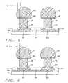
- FIGS. 1 through 4show an example of one of the methods that is used to create an interconnect bump.
- a semiconductor surface 10has been provided with a metal contact pad 14 , the semiconductor surface 10 is protected with a layer 12 of passivation.
- An opening 19has been created in the layer 12 of passivation, the surface of the metal contact pad 14 is exposed through this opening 19 .
- a dielectric layer 16is deposited over the surface of the layer 12 of passivation.
- the layer 16 of dielectricis patterned and etched, creating an opening 21 in the layer 16 of dielectric that aligns with the metal pad 14 and that partially exposes the surface of the metal pad 14 .
- a layer 18 of metalis created over the layer 16 of dielectric, layer 18 of metal is in contact with the surface of the metal pad 14 inside opening 21 .
- the region of layer 18 of metal that is above the metal pad 14will, at a later point in the processing, form a pedestal over which the interconnect bump will be formed.
- This pedestalcan be further extended in a vertical direction by the deposition and patterning of one or more additional layers that may contain a photoresist or a dielectric material, these additional layers are not shown in FIG. 2 .
- These layersessentially have the shape of layer 16 and are removed during one of the final processing steps that is applied for the formation of the interconnect bump.
- a layer of photoresist(not shown) is deposited, patterned and etched, creating an opening that aligns with the contact pad 14 .
- a layer 20 of metalsuch as copper or nickel, FIG. 3 , that forms an integral part of the pedestal of the to be created interconnect bump, is next electroplated in the opening created in the layer of photoresist and on the surface of the layer 18 of metal, whereby the layer 18 serves as the lower electrode during the plating process.
- Layer 20 in prior art applicationshas a thickness of between about 1 and 10 micrometers with a typical value of about 5 micrometers.
- the final layer 22 of solderis electroplated on the surface of layer 20 .
- the patterned layer of photoresistis then removed.
- the layer 18 of metalis next etched, FIG. 4 , leaving in place only the pedestal for the interconnect bump. During this etch process the deposited layers 20 and 22 serve as a mask. If, as indicated above, additional layers of dielectric or photoresist have been deposited for the further shaping of pedestal 18 in FIG. 2 , these layers are also removed at this time.
- solder paste or flux(not shown) is now applied to the layer 22 of solder, the solder 22 is melted in a reflow surface typically under a nitrogen atmosphere, creating the spherically shaped interconnect bump 22 that is shown in FIG. 4 .
- BLM layersare successive and overlying layers of chrome, copper and gold, whereby the chrome is used to enhance adhesion with an underlying aluminum contact pad, the copper layer serves to prevent diffusion of solder materials into underlying layers while the gold layer serves to prevent oxidation of the surface of the copper layer.
- the BLM layeris layer 18 of FIGS. 2 through 4 .
- Increased device densitybrings with it increased closeness of components and elements that are part of the created semiconductor devices. This increased closeness is expressed as a reduction in the spacing or “pitch” between elements of a semiconductor device.
- State-of-the-art technologyuses solder bumps having a pitch of about 200 micrometers, which imposes a limitation on further increasing device density.
- the limitation in further reducing the pitch of solder bumpsis imposed by concerns of reliability, which impose a relatively large ball size for the solder bump. This relatively large solder ball restricts further reducing the solder ball pitch.
- solder bumpsare used as interconnections between I/O bond pads and a substrate or printed circuit board.
- Large solder ballsbring with it high standoff since a solder ball with high standoff has better thermal performance (CTE mismatching is easier to avoid resulting in reduced thermal stress on the solder balls).
- Large solder ballsare therefore required in order to maintain interconnect reliability.
- Low-alpha solderis applied to avoid soft error (electrical or functional errors) from occurring, thereby eliminating the potential for inadvertent memory discharge and incorrect setting of the voltage (1 or 0).
- U.S. Pat. No. 6,162,652(Dass et al.) provides for the testing of an integrated circuit device including depositing a solder bump on a surface of a bond pad.
- U.S. Pat. No. 5,756,370(Farnworth et al.) provides a compliant contact system for making temporary connection with a semiconductor die for testing and a method for fabricating the pliable contact system.
- U.S. Pat. No. 5,554,940(Hubacker) addresses the probing of semiconductor devices that have been provided with contact bumps and the formation of peripheral test pads.
- a principal objective of the inventionis to provide a method of creating a fine-pitch solder bump.
- Another objective of the inventionis to provide a method of creating smaller solder bumps, further allowing for the creation of fine-pitched solder bumps.
- Another objective of the inventionis to provide a cost-effective method to create a fine-pitch solder bump of high reliability, due to the increased height of the solder bump. This objective is based on the believe that solder bump reliability improves proportionally to the square of the distance between the solder ball and the underlying substrate.
- Another objective of the inventionis to provide a cost-effective way of creating a solder bump. This cost-effective way is realized by using standard solder material and therewith eliminating the need for expensive “low-.alpha. solder”.
- Another objective of the inventionis to provide a cost-effective method of creating a fine-pitch solder bump by reducing the alpha-effect on memory products.
- Another objective of the inventionis to provide a method of creating solder bumps which allows an easy method of cleaning flux after the process of creating the solder bump has been completed.
- Another objective of the inventionis to provide a method of creating solder bumps which allows easy application of underfill.
- a contact padis formed on a semiconductor surface, overlying a layer of dielectric.
- a layer of passivationis deposited over the layer of dielectric for the protection of the contact pad, an opening is created in the layer of passivation that partially exposes the surface of the contact pad.
- a barrier layeris deposited over the layer of passivation including the opening created in the layer of passivation.
- a column of three layers of metalis formed overlying the barrier layer and aligned with the contact pad and having a diameter that is about equal to the surface of the contact pad.
- the three metal layers of the columncomprise, in succession when proceeding from the layer that is in contact with the barrier layer, a layer of pillar metal, a layer of under bump metal and a layer of solder metal.
- the layer of pillar metalis reduced in diameter, the barrier layer is selectively removed from the surface of the layer of passivation after which reflowing of the solder metal completes the solder bump of the invention.
- FIGS. 1 through 4show a prior art method of creating a solder bump overlying a point of electrical contact, as follows:
- FIG. 1shows a cross section of a semiconductor surface on the surface of which a contact pad has been created, the semiconductor surface is covered with a patterned layer of passivation.
- FIG. 2shows the cross section of FIG. 1 after a patterned layer of dielectric and a layer of metal have been created on the semiconductor surface.
- FIG. 3shows a cross section of FIG. 2 after a layer of bump metal and solder compound have been selectively deposited.
- FIG. 4show a cross section after excessive layers have been removed from the semiconductor surface and after the solder has been reflowed, forming the interconnect bump.
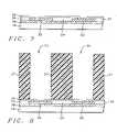
- FIGS. 5 through 16address the invention, as follows:
- FIGS. 5 and 6show a cross section of completed solder bumps of the invention.
- FIG. 7shows a cross section of a semiconductor surface, a layer of dielectric has been deposited, metal pads have been created, a layer of passivation has been deposited and patterned, a layer of barrier material has been deposited.
- FIG. 8shows a cross section after a patterned layer of photoresist has been created over the structure of FIG. 7 .
- FIG. 9shows a cross section after pillar metal has been created aligned with the metal pads, under bump metal has been deposited over the surface of the pillar metal.
- FIG. 10shows a cross section after solder metal has been plated over the under bump metal.
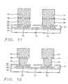
- FIG. 11shows a cross section after the patterned layer of photoresist has been removed from the surface.
- FIG. 12shows a cross section after the diameter of the pillar metal has been reduced.
- FIG. 13shows a cross section after the barrier layer has been etched using isotropic etching, creating a first profile.
- FIG. 14shows a cross section after the barrier layer has been etched using anisotropic etching or RIE, creating a second profile.
- FIG. 15shows a cross-section after the solder metal of the first profile has been reflowed.
- FIG. 16shows a cross-section after the solder metal of the second profile has been reflowed.
- FIG. 5there is shown a cross section of completed solder bumps of the invention having a first profile.
- profilerefers to the difference in which, during one of the final steps of the creation of the solder bumps, the layer of barrier metal is etched.
- an isotropic etch of the exposed barrier metalis performed, removing the exposed barrier metal except for where this barrier metal underlies the pillar metal of the invention.
- an anisotropic etch of the exposed barrier metalis performed, removing the exposed barrier metal except where the barrier metal is shielded from the anisotropic etch by the solder bump, prior to reflow of the solder bump.
- solder bump of the inventionShown in cross section in FIG. 5 is the first profile of the solder bump of the invention, the elements of this solder bump are:
- the semiconductor surface over which the solder bump is createdtypically the surface of a silicon semiconductor substrate
- barrier metalan isotropically etched layer of barrier metal; because this layer of barrier metal has been isotropically etched, the barrier metal has been completely removed from the surface of the layer 34 of passivation except where the barrier metal is covered by the overlying pillar metal ( 38 ) of the solder bump
- the elements of this solder bumpare the same as the elements that have been described above for the first profile of the solder bump of the invention with the exception of layer 35 which is an anisotropically etched layer of barrier metal which, due to the nature of the anisotropic etch, protrudes for the pillar metal 38 as shown in the cross section of FIG. 6 .
- FIGS. 7 through 16provide detail of the process of the invention which leads to the solder bumps that have been shown in cross section in FIGS. 5 and 6 .
- FIG. 7shows a cross section of substrate 10 on the surface, the following elements are highlighted:
- the metal contact padstypically comprising aluminum, created over the surface of the layer 30 of dielectric
- dielectric material for layer 30can be used any of the typically applied dielectrics such as silicon dioxide (doped or undoped), silicon oxynitride, parylene or polyimide, spin-on-glass, plasma oxide or LPCVD oxide.
- the material that is used for the deposition of layer 30 of dielectric of the inventionis not limited to the materials indicated above but can include any of the commonly used dielectrics in the art.
- metal contact pads 32can use conventional methods of metal rf sputtering at a temperature between about 100 and 400 degrees C. and a pressure between about 1 and 100 mTorr using as source for instance aluminum-copper material (for the creation of aluminum contact pads) at a flow rate of between about 10 and 400 sccm to a thickness between about 4000 and 11000 Angstrom. After a layer of metal has been deposited, the layer must be patterned and etched to create the aluminum contact pads 32 . This patterning and etching uses conventional methods of photolithography and patterning and etching.
- a deposited layer of AlCucan be etched using Cl 2 /Ar as an etchant at a temperature between 50 and 200 degrees C., an etchant flow rate of about 20 sccm for the Cl 2 and 1000 sccm for the Ar, a pressure between about 50 mTorr and 10 Torr, a time of the etch between 30 and 200 seconds.
- insulating layerssuch as silicon oxide and oxygen-containing polymers, are deposited using Chemical Vapor Deposition (CVD) technique over the surface of various layers of conducting lines in a semiconductor device or substrate to separate the conductive interconnect lines from each other.
- the insulating layerscan also deposited over patterned layers of interconnecting lines, electrical contact between successive layers of interconnecting lines is established with metal vias created in the insulating layers.
- Electrical contact to the chipis typically established by means of bonding pads or contact pads that form electrical interfaces with patterned levels of interconnecting metal lines. Signal lines and power/ground lines can be connected to the bonding pads or contact pads.
- the bonding pads or contact padsare passivated and electrically insulated by the deposition of a passivation layer over the surface of the bonding pads.
- a passivation layercan contain silicon oxide/silicon nitride (SiO 2 /Si 3 N 4 ) deposited by CVD.
- the passivation layeris patterned and etched to create openings in the passivation layer for the bonding pads or contact pads after which a second and relatively thick passivation layer can be deposited for further insulation and protection of the surface of the chips from moisture and other contaminants and from mechanical damage during assembling of the chips.
- Passivation layercan contain silicon oxide/silicon nitride (SiO 2 /Si 3 N 4 ) deposited by CVD, a passivation layer can be a layer of photosensitive polyimide or can comprise titanium nitride. Another material often used for a passivation layer is phosphorous doped silicon dioxide that is typically deposited over a final layer of aluminum interconnect using a Low Temperature CVD process.
- photosensitive polyimidehas frequently been used for the creation of passivation layers.
- Conventional polyimideshave a number of attractive characteristics for their application in a semiconductor device structure, which have been highlighted above.
- Photosensitive polyimideshave these same characteristics but can, in addition, be patterned like a photoresist mask and can, after patterning and etching, remain on the surface on which it has been deposited to serve as a passivation layer.
- a precursor layeris first deposited by, for example, conventional photoresist spin coating.
- the precursoris, after a low temperature pre-bake, exposed using, for example, a step and repeat projection aligner and Ultra Violet (UV) light as a light source.
- UVUltra Violet
- the portions of the precursor that have been exposed in this mannerare cross-linked, thereby leaving unexposed regions (that are not cross-linked) over the bonding pads.
- the unexposed polyimide precursor layeris dissolved, thereby providing openings over the bonding pads.
- a final step of thermal curingleaves a permanent high quality passivation layer of polyimide over the substrate.
- the preferred material of the invention for the deposition of layer 34 of passivationis Plasma Enhanced silicon nitride (PE Si 3 N 4 ), deposited using PECVD technology at a temperature between about 350 and 450 degrees C. with a pressure of between about 2.0 and 2.8 Torr for the duration between about 8 and 12 seconds.
- Layer 32 of PE Si 3 N 4can be deposited to a thickness between about 200 and 800 Angstrom.
- Layer 34 of PE Si 3 N 4is next patterned and etched to create openings in the layer 34 that overlay and align with the underlying contact pads 32 .
- the etching of layer 34 of passivationcan use Ar/CF 4 as an etchant at a temperature of between about 120 and 160 degrees C. and a pressure of between about 0.30 and 0.40 Torr for a time of between about 33 and 39 seconds using a dry etch process.
- the etching of layer 34 of passivationcan also use He/NF 3 as an etchant at a temperature of between about 80 and 100 degrees C. and a pressure of between about 1.20 and 1.30 Torr for a time of between about 20 and 30 seconds using a dry etch process.
- Barrier layerssuch as layer 36 are typically used to prevent diffusion of an interconnect metal into surrounding layers of dielectric and silicon.
- Some of the considerations that apply in selecting a material for the barrier layerbecome apparent by using copper for interconnect metal as an example. Although copper has a relatively low cost and low resistivity, it has a relatively large diffusion coefficient into silicon dioxide and silicon and is therefore not typically used as an interconnect metal. Copper from an interconnect may diffuse into the silicon dioxide layer causing the dielectric to be conductive and decreasing the dielectric strength of the silicon dioxide layer. Copper interconnects should be encapsulated by at least one diffusion barrier to prevent diffusion into the silicon dioxide layer.
- Silicon nitrideis a diffusion barrier to copper, but the prior art teaches that the interconnects should not lie on a silicon nitride layer because it has a high dielectric constant compared with silicon dioxide. The high dielectric constant causes a desired increase in capacitance between the interconnect and the substrate.
- a typical diffusion barrier layermay contain silicon nitride, phosphosilicate glass (PSG), silicon oxynitride, aluminum, aluminum oxide (Al x O y ), tantalum, Ti/TiN or Ti/W, nionbium, or molybdenum and is more preferably formed from TiN.
- the barrier layercan also be used to improve the adhesion of the subsequent overlying tungsten layer.
- a barrier layeris preferably about 500 and 2000 angstrom thick and more preferably about 300 angstrom thick and can be deposited using rf sputtering.
- a seed layer(not shown in FIG. 7 ) can be blanket deposited over the surface of the wafer.
- any of the conventional metallic seed materialscan be used.
- the metallic seed layercan be deposited using a sputter chamber or an Ion Metal Plasma (IMP) chamber at a temperature of between about 0 and 300 degrees C. and a pressure of between about 1 and 100 mTorr, using (for instance) copper or a copper alloy as the source (as highlighted above) at a flow rate of between about 10 and 400 sccm and using argon as an ambient gas.
- IMPIon Metal Plasma
- FIG. 8shows a cross section of the substrate after a layer 37 of photoresist has been deposited over the surface of the barrier layer 36 .
- the layer 37 of photoresisthas been patterned and etched, creating openings 31 in the layer 37 of photoresist. Openings 31 partially expose the surface of the barrier layer 36 .
- Layer 37 of photoresistis typically applied to a thickness of between about 100 and 200 micrometers but more preferably to a thickness of about 150 micrometers.
- Layer 37 of photoresist Layer 37is typically applied to a thickness of between about 100 and 200 micrometers but more preferably to a thickness of about 150 micrometers.
- the methods used for the deposition and development of the layer 37 of photoresistuses conventional methods of photolithography. Photolithography is a common approach wherein patterned layers are formed by spinning on a layer of photoresist, projecting light through a photomask with the desired pattern onto the photoresist to expose the photoresist to the pattern, developing the photoresist, washing off the undeveloped photoresist, and plasma etching to clean out the areas where the photoresist has been washed away.
- the exposed resistmay be rendered soluble (positive working) and washed away, or insoluble (negative working) and form the pattern.
- the deposited layer 37 of photoresistcan, prior to patterning and etching, be cured or pre-baked further hardening the surface of the layer 37 of photoresist.
- Layer 37 of photoresistcan be etched by applying O 2 plasma and then wet stripping by using H 2 SO 4 , H 2 O 2 and NH 4 OH solution.
- Sulfuric acid (H 2 SO 4 ) and mixtures of H 2 SO 4 with other oxidizing agents such as hydrogen peroxide (H 2 O 2 )are widely used in stripping photoresist after the photoresist has been stripped by other means.
- Wafers to be strippedcan be immersed in the mixture at a temperature between about 100 degrees C. and about 150 degrees C. for 5 to 10 minutes and then subjected to a thorough cleaning with deionized water and dried by dry nitrogen.
- Inorganic resist strippers, such as the sulfuric acid mixturesare very effective in the residual free removal of highly postbaked resist. They are more effective than organic strippers and the longer the immersion time, the cleaner and more residue free wafer surface can be obtained.
- the photoresist layer 37can also be partially removed using plasma oxygen ashing and careful wet clean.
- the oxygen plasma ashingis heating the photoresist in a highly oxidized environment, such as an oxygen plasma, thereby converting the photoresist to an easily removed ash.
- the oxygen plasma ashingcan be followed by a native oxide dip for 90 seconds in a 200:1 diluted solution of hydrofluoric acid.
- FIG. 9shows a cross section of the substrate 10 after a layer 38 of pillar metal has been deposited (electroplated) over the surface of the layer 36 of barrier material and bounded by openings 31 that have been created in the layer 37 of photoresist.
- layers 40 of under bump metalhave been deposited using deposition methods such as electroplating.
- Layer 36preferably comprises titanium or copper and is preferably deposited to a thickness of between about 500 and 2000 angstrom and more preferably to a thickness of about 1000 Angstrom.
- Layer 38preferably comprise copper and is preferred to be applied to a thickness of between about 10 and 100 micrometers but more preferably to a thickness of about 50 micrometers.
- Layer 40preferably comprises nickel and is preferred to be applied to a thickness of between about 1 and 10 micrometers but more preferably to a thickness of about 4 micrometers.
- FIG. 10shows a cross section where the process of the invention has further electroplated layers 42 of solder metal over the surface of layers 40 of under bump metal (UBM) and bounded by the openings 31 that have been created in the layer 37 of photoresist.
- UBMunder bump metal
- Layer 40 of UBMtypically of nickel and of a thickness between about 1 and 10 micrometers, is electroplated over the layer 38 of pillar metal.
- the layer 42 of bump metal(typically solder) is electroplated in contact with the layer 40 of UBM to a thickness of between about 30 and 100 micrometers but more preferably to a thickness of about 50 micrometers.
- the layers 38 , 40 and 42 of electroplated metalare centered in the opening 31 that has been created in the layer 37 of photoresist.
- the patterned layer 37 of photoresisthas been removed from above the surface of the barrier layer 36 .
- the previously highlighted methods and processing conditions for the removal of a layer of photoresistcan be applied for the purpose of the removal of layer 37 that is shown in cross section in FIG. 11 .
- the inventionfurther proceeds with the partial etching of the pillar metal 38 , as shown in cross section in FIG. 12 , using methods of wet chemical etching or an isotropic dry etch, selective to the pillar metal material. It is clear that, by adjusting the etching parameters, of which the time of etch is most beneficial, the diameter of the pillar metal 38 can be reduced by almost any desired amount.
- the limitation that is imposed on the extent to which the diameter of the pillar metal 38 is reducedis not imposed by the wet etching process but by concerns of metal bump reliability and functionality. Too small a remaining diameter of the pillar metal 38 will affect the robustness of the solder bumps while this may also have the affect of increasing the resistance of the metal bump.
- FIGS. 13 and 14The final two processing steps of the invention, before the solder metal is reflowed, are shown in the cross section of FIGS. 13 and 14 and affect the etching of the exposed surface of the barrier layer 36 .
- isotropic etchingFIG. 13
- anisotropic etchingFIG. 14
- the etching of the barrier layeris partially impeded by the presence of the columns 42 of solder metal.
- the undercut shape of pillar 38will prevent wetting of pillar 38 and the UBM layer 40 during subsequent solder reflow. It is also believed that exposure to air will oxidize the sidewalls of pillar 38 and UBM layer 40 and therefore prevent wetting of these surfaces during subsequent solder reflow.
- the sidewalls of pillar 38 and UBM layer 40may be further oxidized by, for example, a thermal oxidation below reflow temperature of about 240 degrees C. such as heating in oxygen ambient at about 125 degrees C.
- FIGS. 15 and 16show the final cross section of the solder bump of the invention after the solder metal has been reflowed.
- FIG. 15corresponds to FIG. 13 while FIG. 16 corresponds to FIG. 14 , this relating to the etch in the barrier layer 36 that has been explained using FIGS. 13 and 14 .
- the etched layer 36 of barrier material that is shown in cross section in FIG. 15corresponds to the etched layer of barrier material that is shown in FIG. 13 .
- FIGS. 16 and 14show the same correspondence exists between FIGS. 16 and 14 .
- a semiconductor surfaceis provided, a layer of dielectric has been deposited over the semiconductor surface, a contact pad has been provided on the layer of dielectric, the contact pad has an exposed surface, a layer of passivation has been deposited over a semiconductor surface including the surface of said contact pad, the layer of passivation has been patterned and etched, creating an opening in the layer of passivation, partially exposing the surface of the contact pad, the opening in the layer of passivation is centered with respect to the contact pad
- the inventionstarts with a barrier layer deposited over the surface of the layer of passivation, making contact with the contact pad through the opening created in the layer of passivation
- a layer of photoresistis deposited over the surface of the barrier layer
- the layer of photoresistis patterned and etched, creating an opening through the layer of photoresist, the opening in the layer of photoresist aligns with and is centered with respect to the contact pad
- the patterned layer of photoresistis removed from the surface of the barrier layer
- the layer of pillar metalis etched, reducing the diameter of the pillar metal
- the barrier layeris etched, using either isotropic or anisotropic etching
- the solder metalis reflowed.
- ball heightis a very important reliability concern; in order to prevent thermal mismatch between overlying layers of a package (such as a semiconductor device and an underlying printed circuit board and the like) it is important to increase the distance between overlying elements; the invention provides this ability
- the solderis, using the invention, relatively far removed from the semiconductor device which means that the application of low-alpha solder is not required (alpha-particles create soft errors in memory products, lead is known to emit alpha-particles when lead decays)
- pillar metala metal needs to be selected that has good conductivity and good ductility, such as copper. This is in order to provide improved thermal performance by counteracting thermal stress
- the height of the pillar of the solder bump of the inventionis important and should be between about 10 to 100 micrometers in order to achieve objectives of high stand-off
- the metal that is used for the under bump metal layeris important in that this metal must have good adhesion with the overlying solder during solder reflow while this metal must not solve too fast and in so doing form a barrier to the solder; in addition, the UBM metal when exposed to air can form a layer of protective oxide thus preventing solder wetting to the pillar metal around the perimeter of the UBM metal during the reflow process; nickel is therefore preferred for the UBM metal
Landscapes
- Engineering & Computer Science (AREA)
- Microelectronics & Electronic Packaging (AREA)
- Power Engineering (AREA)
- Computer Hardware Design (AREA)
- Physics & Mathematics (AREA)
- Condensed Matter Physics & Semiconductors (AREA)
- General Physics & Mathematics (AREA)
- Manufacturing & Machinery (AREA)
- Internal Circuitry In Semiconductor Integrated Circuit Devices (AREA)
- Electric Connection Of Electric Components To Printed Circuits (AREA)
Abstract
Description
- This application is a continuation of application Ser. No. 11/930,998, filed on Oct. 31, 2007, now pending, which is a continuation of application Ser. No. 10/935,451, filed on Sep. 7, 2004, now pending, which is a division of application Ser. No. 09/798,654, filed on Mar. 5, 2001, now Pat. 6,818,545.
- (1) Field of the Invention
- The invention relates to the fabrication of integrated circuit devices, and more particularly, to a method of creating a reliable, fine pitch solder bump at low cost.
- (2) Description of the Prior Art
- Semiconductor device packaging has over the years received increased emphasis due to a continued decrease in semiconductor device feature size, a decrease that is driven by the dual requirements of improved device performance and reduced device manufacturing cost. This trend has led to a significant increase in semiconductor device density, which places increased emphasis on device or package I/O capabilities. The metal connections, which connect the Integrated Circuit to other circuits or to system components, have therefore become more important and can, with further miniaturization of the semiconductor device, have an increasingly negative impact on circuit performance. Increasing parasitic capacitance and resistance of the metal interconnections can significantly degrade chip performance. Of most concern in this respect is the voltage drop along the power and ground buses and the RC delay of the critical signal paths. Attempts to reduce the resistance by using wider metal lines result in higher capacitance of these wires.
- One of the approaches that has been taken to solve these packaging problems is to develop low resistance metals (such as copper) for the interconnect wires, while low dielectric constant materials are being used in between signal lines. Another approach to solve problems of I/O capability has been to design chips and chip packaging techniques that offer dependable methods of increased interconnecting of chips at a reasonable manufacturing cost. This has led to the development of Flip Chip Packages.
- Flip-chip technology fabricates bumps (typically Pb/Sn solders) on Al pads on the chips and interconnects the bumps directly to the package media, which are usually ceramic or plastic based. The flip-chip is bonded face down to the package medium through the shortest paths. These technologies can be applied not only to single-chip packaging, but also to higher or integrated levels of packaging in which the packages are larger, and to more sophisticated substrates that accommodate several chips to form larger functional units.
- The flip-chip technique, using an array of I/O interconnects has the advantage of achieving the highest density of interconnection to the device combined with a very low inductance interconnection to the package. However, pre-testability, post-bonding visual inspection, and Coefficient of Thermal Expansion (CTE) matching to avoid solder bump fatigue are still challenges. In mounting several packages together, such as surface mounting a ceramic package to a plastic board, the TCE mismatch can cause a large thermal stress on the solder-lead joints that can lead to joint breakage caused by solder fatigue from temperature cycling operations.
- Prior Art substrate packaging uses ceramic and plastic flip chip packaging. Ceramic substrate packaging is expensive and has proven to limit the performance of the overall package. Recent years has seen the emergence of plastic substrate flip chip packaging, this type of packaging has become the main stream design and is frequently used in high volume flip chip package fabrication. The plastic substrate flip chip package performs satisfactorily when used for low-density flip chip Integrated Circuits (IC's). If the number of pins emanating from the IC is high, that is in excess of 350 pins, or if the number of pins coming from the IC is less than 350 but the required overall package size is small, the plastic flip chip structure becomes complicated and expensive. This can be traced to the multi-layer structure used to create the plastic flip chip package. This multi-layer structure results in a line density within the package of typically 2-3 mil range. This line density is not sufficiently high for realizing the fan out from the chip I/O to the solder balls on the package within a single layer, leading to the multi-layer approach. The multi-layer approach brings with it the use of relatively thick (50 to 75 micrometers) dielectric layers, these layers have a Coefficient of Thermal Expansion (CTE) that is considerably higher than the CTE of the laminate board on which the plastic flip chip package is mounted. To counteract this difference in CTE's the overall package must be (thermally and mechanically) balanced resulting in the use of additional material and processing steps to apply these materials, increasing the cost of the Ball Grid Array (BGA) package and creating a yield detractor.
- In creating semiconductor devices, the technology of interconnecting devices and device features is a continuing challenge in the era of sub-micron devices. Bond pads and solder bumps are frequently used for this purpose, whereby continuous effort is dedicated to creating bond pads and solder bumps that are simple, reliable and inexpensive.
- Bond pads are generally used to wire device elements and to provide exposed contact regions of the die. These contact regions are suitable for wiring the die to components that are external to the die. An example is where a bond wire is attached to a bond pad of a semiconductor die at one end and to a portion of a Printed Circuit Board at the other end of the wire. The art is constantly striving to achieve improvements in the creation of bond pads that simplify the manufacturing process while enhancing bond pad reliability.
- Materials that are typically used for bond pads include metallic materials, such as tungsten and aluminum, while heavily doped polysilicon can also be used for contacting material. The bond pad is formed on the top surface of the semiconductor device whereby the electrically conducting material is frequently embedded in an insulating layer of dielectric. In using polysilicon as the bond pad material, polysilicon can be doped with an n-type dopant for contacting N-regions while it can be doped with p-type dopant for contacting P-regions. This approach of doping avoids inter-diffusion of the dopants and dopant migration. It is clear that low contact resistance for the bond pad area is required while concerns of avoidance of moisture or chemical solvent absorption, thin film adhesion characteristics, delamination and cracking play an important part in the creation of bond pads.
- The conventional processing sequence that is used to create an aluminum bond pad starts with a semiconductor surface, typically the surface of a silicon single crystalline substrate. A layer of Intra Metal Dielectric (IMD) is deposited over the surface, a layer of metal, typically aluminum, is deposited over the surface of the layer of IMD. The layer of metal is patterned and etched typically using a layer of photoresist and conventional methods of photolithography and etching. After a bond pad has been created in this manner, a layer of passivation is deposited over the layer of IMD. An opening that aligns with the bond pad is created in the layer of passivation, again using methods of photolithography and etching.
- A conventional method that is used to create a solder bump over a contact pad is next highlighted.
FIGS. 1 through 4 show an example of one of the methods that is used to create an interconnect bump. Asemiconductor surface 10 has been provided with ametal contact pad 14, thesemiconductor surface 10 is protected with alayer 12 of passivation. Anopening 19 has been created in thelayer 12 of passivation, the surface of themetal contact pad 14 is exposed through thisopening 19. Next,FIG. 2 , adielectric layer 16 is deposited over the surface of thelayer 12 of passivation. Thelayer 16 of dielectric is patterned and etched, creating anopening 21 in thelayer 16 of dielectric that aligns with themetal pad 14 and that partially exposes the surface of themetal pad 14. Alayer 18 of metal, typically using Under-Bump-Metallurgy (UBM), is created over thelayer 16 of dielectric,layer 18 of metal is in contact with the surface of themetal pad 14 inside opening21. The region oflayer 18 of metal that is above themetal pad 14 will, at a later point in the processing, form a pedestal over which the interconnect bump will be formed. This pedestal can be further extended in a vertical direction by the deposition and patterning of one or more additional layers that may contain a photoresist or a dielectric material, these additional layers are not shown inFIG. 2 . These layers essentially have the shape oflayer 16 and are removed during one of the final processing steps that is applied for the formation of the interconnect bump. - A layer of photoresist (not shown) is deposited, patterned and etched, creating an opening that aligns with the
contact pad 14. Alayer 20 of metal, such as copper or nickel,FIG. 3 , that forms an integral part of the pedestal of the to be created interconnect bump, is next electroplated in the opening created in the layer of photoresist and on the surface of thelayer 18 of metal, whereby thelayer 18 serves as the lower electrode during the plating process.Layer 20 in prior art applications has a thickness of between about 1 and 10 micrometers with a typical value of about 5 micrometers. Thefinal layer 22 of solder is electroplated on the surface oflayer 20. The patterned layer of photoresist is then removed. - The
layer 18 of metal is next etched,FIG. 4 , leaving in place only the pedestal for the interconnect bump. During this etch process the deposited layers20 and22 serve as a mask. If, as indicated above, additional layers of dielectric or photoresist have been deposited for the further shaping ofpedestal 18 inFIG. 2 , these layers are also removed at this time. - A solder paste or flux (not shown) is now applied to the
layer 22 of solder, thesolder 22 is melted in a reflow surface typically under a nitrogen atmosphere, creating the spherically shapedinterconnect bump 22 that is shown inFIG. 4 . - In addition to the above indicated additional layers of dielectric or photoresist that can be used to further shape the pedestal of the interconnect bump, many of the applications that are aimed at creating interconnect bumps make use of layers of metal that serve as barrier layers or that have other specific purposes, such as the improvement of adhesion of the various overlying layers or the prevention of diffusion of materials between adjacent layers. These layers collectively form
layer 18 ofFIG. 4 and have, as is clear from the above, an effect on the shape of the completed bump and are therefore frequently referred to as Ball Limiting Metal (BLM) layer. Frequently used BLM layers are successive and overlying layers of chrome, copper and gold, whereby the chrome is used to enhance adhesion with an underlying aluminum contact pad, the copper layer serves to prevent diffusion of solder materials into underlying layers while the gold layer serves to prevent oxidation of the surface of the copper layer. The BLM layer islayer 18 ofFIGS. 2 through 4 . - Increased device density brings with it increased closeness of components and elements that are part of the created semiconductor devices. This increased closeness is expressed as a reduction in the spacing or “pitch” between elements of a semiconductor device. State-of-the-art technology uses solder bumps having a pitch of about 200 micrometers, which imposes a limitation on further increasing device density. The limitation in further reducing the pitch of solder bumps is imposed by concerns of reliability, which impose a relatively large ball size for the solder bump. This relatively large solder ball restricts further reducing the solder ball pitch.
- In the majority of applications, solder bumps are used as interconnections between I/O bond pads and a substrate or printed circuit board. Large solder balls bring with it high standoff since a solder ball with high standoff has better thermal performance (CTE mismatching is easier to avoid resulting in reduced thermal stress on the solder balls). Large solder balls are therefore required in order to maintain interconnect reliability. Low-alpha solder is applied to avoid soft error (electrical or functional errors) from occurring, thereby eliminating the potential for inadvertent memory discharge and incorrect setting of the voltage (1 or 0).
- U.S. Pat. No. 6,162,652 (Dass et al.) provides for the testing of an integrated circuit device including depositing a solder bump on a surface of a bond pad.
- U.S. Pat. No. 5,756,370 (Farnworth et al.) provides a compliant contact system for making temporary connection with a semiconductor die for testing and a method for fabricating the pliable contact system.
- U.S. Pat. No. 5,554,940 (Hubacker) addresses the probing of semiconductor devices that have been provided with contact bumps and the formation of peripheral test pads.
- U.S. Pat. No. 5,665,639 (Seppala et al.), U.S. Pat. No. 6,051,450 (Ohsawa et al.) and U.S. Pat. No. 5,882,957 (Lin) show related bump processes.
- U.S. Pat. No. 5,633,535 (Chao et al.) shows a pedestal process using dry resist.
- U.S. Pat. No. 6,103,552 (Lin) provides a process and package for achieving wafer scale packaging, which includes formation of a solder bump.
- A principal objective of the invention is to provide a method of creating a fine-pitch solder bump.
- Another objective of the invention is to provide a method of creating smaller solder bumps, further allowing for the creation of fine-pitched solder bumps.
- Another objective of the invention is to provide a cost-effective method to create a fine-pitch solder bump of high reliability, due to the increased height of the solder bump. This objective is based on the believe that solder bump reliability improves proportionally to the square of the distance between the solder ball and the underlying substrate.
- Another objective of the invention is to provide a cost-effective way of creating a solder bump. This cost-effective way is realized by using standard solder material and therewith eliminating the need for expensive “low-.alpha. solder”.
- Another objective of the invention is to provide a cost-effective method of creating a fine-pitch solder bump by reducing the alpha-effect on memory products.
- Another objective of the invention is to provide a method of creating solder bumps which allows an easy method of cleaning flux after the process of creating the solder bump has been completed.
- Another objective of the invention is to provide a method of creating solder bumps which allows easy application of underfill.
- In accordance with the process of the invention, a contact pad is formed on a semiconductor surface, overlying a layer of dielectric. A layer of passivation is deposited over the layer of dielectric for the protection of the contact pad, an opening is created in the layer of passivation that partially exposes the surface of the contact pad. A barrier layer is deposited over the layer of passivation including the opening created in the layer of passivation. A column of three layers of metal is formed overlying the barrier layer and aligned with the contact pad and having a diameter that is about equal to the surface of the contact pad. The three metal layers of the column comprise, in succession when proceeding from the layer that is in contact with the barrier layer, a layer of pillar metal, a layer of under bump metal and a layer of solder metal. The layer of pillar metal is reduced in diameter, the barrier layer is selectively removed from the surface of the layer of passivation after which reflowing of the solder metal completes the solder bump of the invention.
FIGS. 1 through 4 show a prior art method of creating a solder bump overlying a point of electrical contact, as follows:FIG. 1 shows a cross section of a semiconductor surface on the surface of which a contact pad has been created, the semiconductor surface is covered with a patterned layer of passivation.FIG. 2 shows the cross section ofFIG. 1 after a patterned layer of dielectric and a layer of metal have been created on the semiconductor surface.FIG. 3 shows a cross section ofFIG. 2 after a layer of bump metal and solder compound have been selectively deposited.FIG. 4 show a cross section after excessive layers have been removed from the semiconductor surface and after the solder has been reflowed, forming the interconnect bump.FIGS. 5 through 16 address the invention, as follows:FIGS. 5 and 6 show a cross section of completed solder bumps of the invention.FIG. 7 shows a cross section of a semiconductor surface, a layer of dielectric has been deposited, metal pads have been created, a layer of passivation has been deposited and patterned, a layer of barrier material has been deposited.FIG. 8 shows a cross section after a patterned layer of photoresist has been created over the structure ofFIG. 7 .FIG. 9 shows a cross section after pillar metal has been created aligned with the metal pads, under bump metal has been deposited over the surface of the pillar metal.FIG. 10 shows a cross section after solder metal has been plated over the under bump metal.FIG. 11 shows a cross section after the patterned layer of photoresist has been removed from the surface.FIG. 12 shows a cross section after the diameter of the pillar metal has been reduced.FIG. 13 shows a cross section after the barrier layer has been etched using isotropic etching, creating a first profile.FIG. 14 shows a cross section after the barrier layer has been etched using anisotropic etching or RIE, creating a second profile.FIG. 15 shows a cross-section after the solder metal of the first profile has been reflowed.FIG. 16 shows a cross-section after the solder metal of the second profile has been reflowed.- Referring now specifically to
FIG. 5 , there is shown a cross section of completed solder bumps of the invention having a first profile. The term profile refers to the difference in which, during one of the final steps of the creation of the solder bumps, the layer of barrier metal is etched. - For the first profile of the solder bumps of the invention, an isotropic etch of the exposed barrier metal is performed, removing the exposed barrier metal except for where this barrier metal underlies the pillar metal of the invention.
- For the second profile of the solder bumps of the invention, an anisotropic etch of the exposed barrier metal is performed, removing the exposed barrier metal except where the barrier metal is shielded from the anisotropic etch by the solder bump, prior to reflow of the solder bump.
- Shown in cross section in
FIG. 5 is the first profile of the solder bump of the invention, the elements of this solder bump are: - 10, the semiconductor surface over which the solder bump is created, typically the surface of a silicon semiconductor substrate
- 30, a layer of dielectric that has been deposited over the
semiconductor surface 10 - 32, contact pads that have been created on the surface of the
layer 30 of dielectric - 34, a patterned layer of passivation that has been deposited over the surface of the
layer 30 of dielectric; openings have been created in thelayer 34 of passivation, partially exposing the surface ofcontact pads 32 - 36, an isotropically etched layer of barrier metal; because this layer of barrier metal has been isotropically etched, the barrier metal has been completely removed from the surface of the
layer 34 of passivation except where the barrier metal is covered by the overlying pillar metal (38) of the solder bump - 38, the pillar metal of the solder bump
- 40, a layer of under bump metal created overlying the
pillar metal 38 of the solder bump - 42, the solder metal.
- Shown in cross section in
FIG. 6 is the second profile of the solder bump of the invention, the elements of this solder bump are the same as the elements that have been described above for the first profile of the solder bump of the invention with the exception oflayer 35 which is an anisotropically etched layer of barrier metal which, due to the nature of the anisotropic etch, protrudes for thepillar metal 38 as shown in the cross section ofFIG. 6 . FIGS. 7 through 16 provide detail of the process of the invention which leads to the solder bumps that have been shown in cross section inFIGS. 5 and 6 .FIG. 7 shows a cross section ofsubstrate 10 on the surface, the following elements are highlighted:- 10, a silicon substrate over the surface of which
metal contact pads 32 have been created - 30, a layer of dielectric that has been deposited over the surface of
substrate 10 - 32, the metal contact pads, typically comprising aluminum, created over the surface of the
layer 30 of dielectric - 34, a layer of passivation that has been deposited over the surface of the
layer 30 of dielectric. Openings have been created in thelayer 34 of passivation that align with themetal contact pads 32, partially exposing the surface of thecontact pads 32 - 36, a layer of barrier metal that has been created over the surface of
layer 34 of passivation, including the openings that have been created in thelayer 34 of passivation, contacting theunderlying contact pads 32. - As dielectric material for
layer 30 can be used any of the typically applied dielectrics such as silicon dioxide (doped or undoped), silicon oxynitride, parylene or polyimide, spin-on-glass, plasma oxide or LPCVD oxide. The material that is used for the deposition oflayer 30 of dielectric of the invention is not limited to the materials indicated above but can include any of the commonly used dielectrics in the art. - The creation of
metal contact pads 32 can use conventional methods of metal rf sputtering at a temperature between about 100 and 400 degrees C. and a pressure between about 1 and 100 mTorr using as source for instance aluminum-copper material (for the creation of aluminum contact pads) at a flow rate of between about 10 and 400 sccm to a thickness between about 4000 and 11000 Angstrom. After a layer of metal has been deposited, the layer must be patterned and etched to create thealuminum contact pads 32. This patterning and etching uses conventional methods of photolithography and patterning and etching. A deposited layer of AlCu can be etched using Cl2/Ar as an etchant at a temperature between 50 and 200 degrees C., an etchant flow rate of about 20 sccm for the Cl2and 1000 sccm for the Ar, a pressure between about 50 mTorr and 10 Torr, a time of the etch between 30 and 200 seconds. - In a typical application insulating layers, such as silicon oxide and oxygen-containing polymers, are deposited using Chemical Vapor Deposition (CVD) technique over the surface of various layers of conducting lines in a semiconductor device or substrate to separate the conductive interconnect lines from each other. The insulating layers can also deposited over patterned layers of interconnecting lines, electrical contact between successive layers of interconnecting lines is established with metal vias created in the insulating layers. Electrical contact to the chip is typically established by means of bonding pads or contact pads that form electrical interfaces with patterned levels of interconnecting metal lines. Signal lines and power/ground lines can be connected to the bonding pads or contact pads. After the bonding pads or contact pads have been created on the surfaces of the chip, the bonding pads or contact pads are passivated and electrically insulated by the deposition of a passivation layer over the surface of the bonding pads. A passivation layer can contain silicon oxide/silicon nitride (SiO2/Si3N4) deposited by CVD. The passivation layer is patterned and etched to create openings in the passivation layer for the bonding pads or contact pads after which a second and relatively thick passivation layer can be deposited for further insulation and protection of the surface of the chips from moisture and other contaminants and from mechanical damage during assembling of the chips.
- Various materials have found application in the creation of passivation layers. Passivation layer can contain silicon oxide/silicon nitride (SiO2/Si3N4) deposited by CVD, a passivation layer can be a layer of photosensitive polyimide or can comprise titanium nitride. Another material often used for a passivation layer is phosphorous doped silicon dioxide that is typically deposited over a final layer of aluminum interconnect using a Low Temperature CVD process. In recent years, photosensitive polyimide has frequently been used for the creation of passivation layers. Conventional polyimides have a number of attractive characteristics for their application in a semiconductor device structure, which have been highlighted above. Photosensitive polyimides have these same characteristics but can, in addition, be patterned like a photoresist mask and can, after patterning and etching, remain on the surface on which it has been deposited to serve as a passivation layer. Typically and to improve surface adhesion and tension reduction, a precursor layer is first deposited by, for example, conventional photoresist spin coating. The precursor is, after a low temperature pre-bake, exposed using, for example, a step and repeat projection aligner and Ultra Violet (UV) light as a light source. The portions of the precursor that have been exposed in this manner are cross-linked, thereby leaving unexposed regions (that are not cross-linked) over the bonding pads. During subsequent development, the unexposed polyimide precursor layer (over the bonding pads) is dissolved, thereby providing openings over the bonding pads. A final step of thermal curing leaves a permanent high quality passivation layer of polyimide over the substrate.
- The preferred material of the invention for the deposition of
layer 34 of passivation is Plasma Enhanced silicon nitride (PE Si3N4), deposited using PECVD technology at a temperature between about 350 and 450 degrees C. with a pressure of between about 2.0 and 2.8 Torr for the duration between about 8 and 12 seconds.Layer 32 of PE Si3N4can be deposited to a thickness between about 200 and 800 Angstrom. Layer 34 of PE Si3N4is next patterned and etched to create openings in thelayer 34 that overlay and align with theunderlying contact pads 32.- The etching of
layer 34 of passivation can use Ar/CF4as an etchant at a temperature of between about 120 and 160 degrees C. and a pressure of between about 0.30 and 0.40 Torr for a time of between about 33 and 39 seconds using a dry etch process. - The etching of
layer 34 of passivation can also use He/NF3as an etchant at a temperature of between about 80 and 100 degrees C. and a pressure of between about 1.20 and 1.30 Torr for a time of between about 20 and 30 seconds using a dry etch process. - Barrier layers, such as
layer 36, are typically used to prevent diffusion of an interconnect metal into surrounding layers of dielectric and silicon. Some of the considerations that apply in selecting a material for the barrier layer become apparent by using copper for interconnect metal as an example. Although copper has a relatively low cost and low resistivity, it has a relatively large diffusion coefficient into silicon dioxide and silicon and is therefore not typically used as an interconnect metal. Copper from an interconnect may diffuse into the silicon dioxide layer causing the dielectric to be conductive and decreasing the dielectric strength of the silicon dioxide layer. Copper interconnects should be encapsulated by at least one diffusion barrier to prevent diffusion into the silicon dioxide layer. Silicon nitride is a diffusion barrier to copper, but the prior art teaches that the interconnects should not lie on a silicon nitride layer because it has a high dielectric constant compared with silicon dioxide. The high dielectric constant causes a desired increase in capacitance between the interconnect and the substrate. - A typical diffusion barrier layer may contain silicon nitride, phosphosilicate glass (PSG), silicon oxynitride, aluminum, aluminum oxide (AlxOy), tantalum, Ti/TiN or Ti/W, nionbium, or molybdenum and is more preferably formed from TiN. The barrier layer can also be used to improve the adhesion of the subsequent overlying tungsten layer.
- A barrier layer is preferably about 500 and 2000 angstrom thick and more preferably about 300 angstrom thick and can be deposited using rf sputtering.
- After the creation of
barrier layer 36, a seed layer (not shown inFIG. 7 ) can be blanket deposited over the surface of the wafer. For a seed layer that is blanket deposited over the surface of the wafer any of the conventional metallic seed materials can be used. The metallic seed layer can be deposited using a sputter chamber or an Ion Metal Plasma (IMP) chamber at a temperature of between about 0 and 300 degrees C. and a pressure of between about 1 and 100 mTorr, using (for instance) copper or a copper alloy as the source (as highlighted above) at a flow rate of between about 10 and 400 sccm and using argon as an ambient gas. FIG. 8 shows a cross section of the substrate after alayer 37 of photoresist has been deposited over the surface of thebarrier layer 36. Thelayer 37 of photoresist has been patterned and etched, creatingopenings 31 in thelayer 37 of photoresist.Openings 31 partially expose the surface of thebarrier layer 36.Layer 37 of photoresist is typically applied to a thickness of between about 100 and 200 micrometers but more preferably to a thickness of about 150 micrometers.Layer 37 ofphotoresist Layer 37 is typically applied to a thickness of between about 100 and 200 micrometers but more preferably to a thickness of about 150 micrometers. The methods used for the deposition and development of thelayer 37 of photoresist uses conventional methods of photolithography. Photolithography is a common approach wherein patterned layers are formed by spinning on a layer of photoresist, projecting light through a photomask with the desired pattern onto the photoresist to expose the photoresist to the pattern, developing the photoresist, washing off the undeveloped photoresist, and plasma etching to clean out the areas where the photoresist has been washed away. The exposed resist may be rendered soluble (positive working) and washed away, or insoluble (negative working) and form the pattern.- The deposited
layer 37 of photoresist can, prior to patterning and etching, be cured or pre-baked further hardening the surface of thelayer 37 of photoresist. Layer 37 of photoresist can be etched by applying O2plasma and then wet stripping by using H2SO4, H2O2and NH4OH solution. Sulfuric acid (H2SO4) and mixtures of H2SO4with other oxidizing agents such as hydrogen peroxide (H2O2) are widely used in stripping photoresist after the photoresist has been stripped by other means. Wafers to be stripped can be immersed in the mixture at a temperature between about 100 degrees C. and about 150 degrees C. for 5 to 10 minutes and then subjected to a thorough cleaning with deionized water and dried by dry nitrogen. Inorganic resist strippers, such as the sulfuric acid mixtures, are very effective in the residual free removal of highly postbaked resist. They are more effective than organic strippers and the longer the immersion time, the cleaner and more residue free wafer surface can be obtained.- The
photoresist layer 37 can also be partially removed using plasma oxygen ashing and careful wet clean. The oxygen plasma ashing is heating the photoresist in a highly oxidized environment, such as an oxygen plasma, thereby converting the photoresist to an easily removed ash. The oxygen plasma ashing can be followed by a native oxide dip for 90 seconds in a 200:1 diluted solution of hydrofluoric acid. FIG. 9 shows a cross section of thesubstrate 10 after alayer 38 of pillar metal has been deposited (electroplated) over the surface of thelayer 36 of barrier material and bounded byopenings 31 that have been created in thelayer 37 of photoresist. Over the surface of thelayers 38 of metal, which will be referred to as pillar metal in view of the role these layers play in the completed structure of the solder bumps of the invention, layers40 of under bump metal have been deposited using deposition methods such as electroplating.Layer 36 preferably comprises titanium or copper and is preferably deposited to a thickness of between about 500 and 2000 angstrom and more preferably to a thickness of about 1000 Angstrom.Layer 38 preferably comprise copper and is preferred to be applied to a thickness of between about 10 and 100 micrometers but more preferably to a thickness of about 50 micrometers.Layer 40 preferably comprises nickel and is preferred to be applied to a thickness of between about 1 and 10 micrometers but more preferably to a thickness of about 4 micrometers.FIG. 10 shows a cross section where the process of the invention has further electroplatedlayers 42 of solder metal over the surface oflayers 40 of under bump metal (UBM) and bounded by theopenings 31 that have been created in thelayer 37 of photoresist.Layer 40 of UBM, typically of nickel and of a thickness between about 1 and 10 micrometers, is electroplated over thelayer 38 of pillar metal. Thelayer 42 of bump metal (typically solder) is electroplated in contact with thelayer 40 of UBM to a thickness of between about 30 and 100 micrometers but more preferably to a thickness of about 50 micrometers. Thelayers opening 31 that has been created in thelayer 37 of photoresist.- In the cross section that is shown in
FIG. 11 , it is shown that the patternedlayer 37 of photoresist has been removed from above the surface of thebarrier layer 36. The previously highlighted methods and processing conditions for the removal of a layer of photoresist can be applied for the purpose of the removal oflayer 37 that is shown in cross section inFIG. 11 . The invention further proceeds with the partial etching of thepillar metal 38, as shown in cross section inFIG. 12 , using methods of wet chemical etching or an isotropic dry etch, selective to the pillar metal material. It is clear that, by adjusting the etching parameters, of which the time of etch is most beneficial, the diameter of thepillar metal 38 can be reduced by almost any desired amount. The limitation that is imposed on the extent to which the diameter of thepillar metal 38 is reduced is not imposed by the wet etching process but by concerns of metal bump reliability and functionality. Too small a remaining diameter of thepillar metal 38 will affect the robustness of the solder bumps while this may also have the affect of increasing the resistance of the metal bump. - The final two processing steps of the invention, before the solder metal is reflowed, are shown in the cross section of
FIGS. 13 and 14 and affect the etching of the exposed surface of thebarrier layer 36. Using isotropic etching,FIG. 13 , the exposed barrier layer is completely removed as is shown inFIG. 13 . Using anisotropic etching,FIG. 14 , the etching of the barrier layer is partially impeded by the presence of thecolumns 42 of solder metal. - It is believed that the undercut shape of
pillar 38 will prevent wetting ofpillar 38 and theUBM layer 40 during subsequent solder reflow. It is also believed that exposure to air will oxidize the sidewalls ofpillar 38 andUBM layer 40 and therefore prevent wetting of these surfaces during subsequent solder reflow. Optionally, the sidewalls ofpillar 38 andUBM layer 40 may be further oxidized by, for example, a thermal oxidation below reflow temperature of about 240 degrees C. such as heating in oxygen ambient at about 125 degrees C. FIGS. 15 and 16 show the final cross section of the solder bump of the invention after the solder metal has been reflowed.FIG. 15 corresponds toFIG. 13 whileFIG. 16 corresponds toFIG. 14 , this relating to the etch in thebarrier layer 36 that has been explained usingFIGS. 13 and 14 . It is noted that the etchedlayer 36 of barrier material that is shown in cross section inFIG. 15 corresponds to the etched layer of barrier material that is shown inFIG. 13 . The same correspondence exists betweenFIGS. 16 and 14 .- The above summarized processing steps of electroplating that are used for the creation of a metal bump can be supplemented by the step of curing or pre-baking of the layer of photoresist after this layer has been deposited.
- To review and summarize the invention:
- prior to and in preparation for the invention, a semiconductor surface is provided, a layer of dielectric has been deposited over the semiconductor surface, a contact pad has been provided on the layer of dielectric, the contact pad has an exposed surface, a layer of passivation has been deposited over a semiconductor surface including the surface of said contact pad, the layer of passivation has been patterned and etched, creating an opening in the layer of passivation, partially exposing the surface of the contact pad, the opening in the layer of passivation is centered with respect to the contact pad
- the invention starts with a barrier layer deposited over the surface of the layer of passivation, making contact with the contact pad through the opening created in the layer of passivation
- a layer of photoresist is deposited over the surface of the barrier layer
- the layer of photoresist is patterned and etched, creating an opening through the layer of photoresist, the opening in the layer of photoresist aligns with and is centered with respect to the contact pad
- in sequence are deposited, bounded by the opening created in the layer of photoresist, a layer of pillar metal, a layer of under bump metal and a layer of solder metal
- the patterned layer of photoresist is removed from the surface of the barrier layer
- the layer of pillar metal is etched, reducing the diameter of the pillar metal
- the barrier layer is etched, using either isotropic or anisotropic etching
- the solder metal is reflowed.
- The invention offers the following advantages:
- ball height is a very important reliability concern; in order to prevent thermal mismatch between overlying layers of a package (such as a semiconductor device and an underlying printed circuit board and the like) it is important to increase the distance between overlying elements; the invention provides this ability
- a larger solder ball (for better thermal or reliability performance) results in increased pitch, this is contrary to state of the art design requirements
- if small solder balls are used without providing height, it is very difficult to underfill the small gaps
- the solder is, using the invention, relatively far removed from the semiconductor device which means that the application of low-alpha solder is not required (alpha-particles create soft errors in memory products, lead is known to emit alpha-particles when lead decays)
- for the pillar metal a metal needs to be selected that has good conductivity and good ductility, such as copper. This is in order to provide improved thermal performance by counteracting thermal stress
- the height of the pillar of the solder bump of the invention is important and should be between about 10 to 100 micrometers in order to achieve objectives of high stand-off
- the metal that is used for the under bump metal layer is important in that this metal must have good adhesion with the overlying solder during solder reflow while this metal must not solve too fast and in so doing form a barrier to the solder; in addition, the UBM metal when exposed to air can form a layer of protective oxide thus preventing solder wetting to the pillar metal around the perimeter of the UBM metal during the reflow process; nickel is therefore preferred for the UBM metal
- Although the invention has been described and illustrated with reference to specific illustrative embodiments thereof, it is not intended that the invention be limited to those illustrative embodiments. Those skilled in the art will recognize that variations and modifications can be made without departing from the spirit of the invention. It is therefore intended to include within the invention all such variations and modifications which fall within the scope of the appended claims and equivalents thereof.
Claims (23)
Priority Applications (1)
| Application Number | Priority Date | Filing Date | Title |
|---|---|---|---|
| US12/493,258US8072070B2 (en) | 2001-03-05 | 2009-06-29 | Low fabrication cost, fine pitch and high reliability solder bump |
Applications Claiming Priority (4)
| Application Number | Priority Date | Filing Date | Title |
|---|---|---|---|
| US09/798,654US6818545B2 (en) | 2001-03-05 | 2001-03-05 | Low fabrication cost, fine pitch and high reliability solder bump |
| US10/935,451US8368213B2 (en) | 2001-03-05 | 2004-09-07 | Low fabrication cost, fine pitch and high reliability solder bump |
| US11/930,998US7863739B2 (en) | 2001-03-05 | 2007-10-31 | Low fabrication cost, fine pitch and high reliability solder bump |
| US12/493,258US8072070B2 (en) | 2001-03-05 | 2009-06-29 | Low fabrication cost, fine pitch and high reliability solder bump |
Related Parent Applications (1)
| Application Number | Title | Priority Date | Filing Date |
|---|---|---|---|
| US11/930,998ContinuationUS7863739B2 (en) | 2001-03-05 | 2007-10-31 | Low fabrication cost, fine pitch and high reliability solder bump |
Publications (2)
| Publication Number | Publication Date |
|---|---|
| US20090261473A1true US20090261473A1 (en) | 2009-10-22 |
| US8072070B2 US8072070B2 (en) | 2011-12-06 |
Family
ID=25173939
Family Applications (9)
| Application Number | Title | Priority Date | Filing Date |
|---|---|---|---|
| US09/798,654Expired - LifetimeUS6818545B2 (en) | 2001-03-05 | 2001-03-05 | Low fabrication cost, fine pitch and high reliability solder bump |
| US10/935,451Expired - Fee RelatedUS8368213B2 (en) | 2001-03-05 | 2004-09-07 | Low fabrication cost, fine pitch and high reliability solder bump |
| US11/930,163Expired - LifetimeUS7468316B2 (en) | 2001-03-05 | 2007-10-31 | Low fabrication cost, fine pitch and high reliability solder bump |
| US11/930,149AbandonedUS20080083985A1 (en) | 2001-03-05 | 2007-10-31 | Low fabrication cost, fine pitch and high reliability solder bump |
| US11/930,998Expired - Fee RelatedUS7863739B2 (en) | 2001-03-05 | 2007-10-31 | Low fabrication cost, fine pitch and high reliability solder bump |
| US11/930,156AbandonedUS20080054459A1 (en) | 2001-03-05 | 2007-10-31 | Low fabrication cost, fine pitch and high reliability solder bump |
| US12/098,469AbandonedUS20080188071A1 (en) | 2001-03-05 | 2008-04-07 | Low fabrication cost, fine pitch and high reliability solder bump |
| US12/098,468AbandonedUS20080258305A1 (en) | 2001-03-05 | 2008-04-07 | Low fabrication cost, fine pitch and high reliability solder bump |
| US12/493,258Expired - Fee RelatedUS8072070B2 (en) | 2001-03-05 | 2009-06-29 | Low fabrication cost, fine pitch and high reliability solder bump |
Family Applications Before (8)
| Application Number | Title | Priority Date | Filing Date |
|---|---|---|---|
| US09/798,654Expired - LifetimeUS6818545B2 (en) | 2001-03-05 | 2001-03-05 | Low fabrication cost, fine pitch and high reliability solder bump |
| US10/935,451Expired - Fee RelatedUS8368213B2 (en) | 2001-03-05 | 2004-09-07 | Low fabrication cost, fine pitch and high reliability solder bump |
| US11/930,163Expired - LifetimeUS7468316B2 (en) | 2001-03-05 | 2007-10-31 | Low fabrication cost, fine pitch and high reliability solder bump |
| US11/930,149AbandonedUS20080083985A1 (en) | 2001-03-05 | 2007-10-31 | Low fabrication cost, fine pitch and high reliability solder bump |
| US11/930,998Expired - Fee RelatedUS7863739B2 (en) | 2001-03-05 | 2007-10-31 | Low fabrication cost, fine pitch and high reliability solder bump |
| US11/930,156AbandonedUS20080054459A1 (en) | 2001-03-05 | 2007-10-31 | Low fabrication cost, fine pitch and high reliability solder bump |
| US12/098,469AbandonedUS20080188071A1 (en) | 2001-03-05 | 2008-04-07 | Low fabrication cost, fine pitch and high reliability solder bump |
| US12/098,468AbandonedUS20080258305A1 (en) | 2001-03-05 | 2008-04-07 | Low fabrication cost, fine pitch and high reliability solder bump |
Country Status (3)
| Country | Link |
|---|---|
| US (9) | US6818545B2 (en) |
| EP (1) | EP1239514A3 (en) |
| SG (1) | SG114532A1 (en) |
Cited By (4)
| Publication number | Priority date | Publication date | Assignee | Title |
|---|---|---|---|---|
| US20080235941A1 (en)* | 2007-03-30 | 2008-10-02 | Seng Guan Chow | Integrated circuit package system with mounting features |
| US20100314756A1 (en)* | 2009-06-16 | 2010-12-16 | Mirng-Ji Lii | Interconnect Structures Having Lead-Free Solder Bumps |
| CN102299115A (en)* | 2010-06-24 | 2011-12-28 | 美士美积体产品公司 | Wafer level package (WLP) device having bump assemblies including a barrier metal |
| US11152321B2 (en) | 2019-02-11 | 2021-10-19 | Infineon Technologies Ag | Semiconductor device having a copper pillar interconnect structure |
Families Citing this family (237)
| Publication number | Priority date | Publication date | Assignee | Title |
|---|---|---|---|---|
| US6869870B2 (en) | 1998-12-21 | 2005-03-22 | Megic Corporation | High performance system-on-chip discrete components using post passivation process |
| US8178435B2 (en) | 1998-12-21 | 2012-05-15 | Megica Corporation | High performance system-on-chip inductor using post passivation process |
| ATE459099T1 (en) | 2000-03-10 | 2010-03-15 | Chippac Inc | FLIPCHIP CONNECTION STRUCTURE AND PROCESS OF PRODUCTION THEREOF |
| US10388626B2 (en)* | 2000-03-10 | 2019-08-20 | STATS ChipPAC Pte. Ltd. | Semiconductor device and method of forming flipchip interconnect structure |
| JP2002134545A (en)* | 2000-10-26 | 2002-05-10 | Oki Electric Ind Co Ltd | Semiconductor integrated circuit chip, board and their manufacturing method |
| US7902679B2 (en)* | 2001-03-05 | 2011-03-08 | Megica Corporation | Structure and manufacturing method of a chip scale package with low fabrication cost, fine pitch and high reliability solder bump |
| TWI313507B (en)* | 2002-10-25 | 2009-08-11 | Megica Corporatio | Method for assembling chips |
| US6818545B2 (en) | 2001-03-05 | 2004-11-16 | Megic Corporation | Low fabrication cost, fine pitch and high reliability solder bump |
| US6869515B2 (en) | 2001-03-30 | 2005-03-22 | Uri Cohen | Enhanced electrochemical deposition (ECD) filling of high aspect ratio openings |
| US6732913B2 (en)* | 2001-04-26 | 2004-05-11 | Advanpack Solutions Pte Ltd. | Method for forming a wafer level chip scale package, and package formed thereby |
| US6856007B2 (en) | 2001-08-28 | 2005-02-15 | Tessera, Inc. | High-frequency chip packages |
| US20030116845A1 (en)* | 2001-12-21 | 2003-06-26 | Bojkov Christo P. | Waferlevel method for direct bumping on copper pads in integrated circuits |
| US6696356B2 (en)* | 2001-12-31 | 2004-02-24 | Taiwan Semiconductor Manufacturing Co., Ltd. | Method of making a bump on a substrate without ribbon residue |
| TWI245402B (en)* | 2002-01-07 | 2005-12-11 | Megic Corp | Rod soldering structure and manufacturing process thereof |
| JP3829325B2 (en)* | 2002-02-07 | 2006-10-04 | 日本電気株式会社 | Semiconductor element, manufacturing method thereof, and manufacturing method of semiconductor device |
| AU2003218085A1 (en)* | 2002-03-12 | 2003-09-29 | Fairchild Semiconductor Corporation | Wafer-level coated copper stud bumps |
| US6939789B2 (en)* | 2002-05-13 | 2005-09-06 | Taiwan Semiconductor Manufacturing Co., Ltd. | Method of wafer level chip scale packaging |
| US6774026B1 (en)* | 2002-06-20 | 2004-08-10 | Taiwan Semiconductor Manufacturing Co., Ltd. | Structure and method for low-stress concentration solder bumps |
| WO2004001837A2 (en)* | 2002-06-25 | 2003-12-31 | Unitive International Limited | Methods of forming electronic structures including conductive shunt layers and related structures |
| US20040007779A1 (en)* | 2002-07-15 | 2004-01-15 | Diane Arbuthnot | Wafer-level method for fine-pitch, high aspect ratio chip interconnect |
| US6861749B2 (en)* | 2002-09-20 | 2005-03-01 | Himax Technologies, Inc. | Semiconductor device with bump electrodes |
| US20070273025A1 (en)* | 2002-11-06 | 2007-11-29 | Koninklijke Philips Electronics N.V. | Device Comprising Circuit Elements Connected By Bonding Bump Structure |
| US20040099959A1 (en)* | 2002-11-22 | 2004-05-27 | Hannstar Display Corp. | Conductive bump structure |
| US7387827B2 (en)* | 2002-12-17 | 2008-06-17 | Intel Corporation | Interconnection designs and materials having improved strength and fatigue life |
| TW583759B (en)* | 2003-03-20 | 2004-04-11 | Advanced Semiconductor Eng | Under bump metallurgy and flip chip |
| JP4571781B2 (en)* | 2003-03-26 | 2010-10-27 | ルネサスエレクトロニクス株式会社 | Semiconductor device and manufacturing method thereof |
| US20070264421A1 (en)* | 2003-04-11 | 2007-11-15 | Dieter Meier | Method for Producing Multiple Layer Systems |
| DE10317596A1 (en)* | 2003-04-16 | 2004-11-11 | Epcos Ag | Method for producing solder balls on an electrical component |
| TWI236763B (en)* | 2003-05-27 | 2005-07-21 | Megic Corp | High performance system-on-chip inductor using post passivation process |
| US6972480B2 (en) | 2003-06-16 | 2005-12-06 | Shellcase Ltd. | Methods and apparatus for packaging integrated circuit devices |
| CN100587962C (en) | 2003-07-03 | 2010-02-03 | 泰塞拉技术匈牙利公司 | Method and apparatus for packaging integrated circuit devices |
| US6995475B2 (en)* | 2003-09-18 | 2006-02-07 | International Business Machines Corporation | I/C chip suitable for wire bonding |
| WO2005031861A1 (en) | 2003-09-26 | 2005-04-07 | Tessera, Inc. | Structure and method of making capped chips including a flowable conductive medium |
| US7462942B2 (en)* | 2003-10-09 | 2008-12-09 | Advanpack Solutions Pte Ltd | Die pillar structures and a method of their formation |
| KR100585104B1 (en)* | 2003-10-24 | 2006-05-30 | 삼성전자주식회사 | Manufacturing method of ultra thin flip chip package |
| US20050116344A1 (en)* | 2003-10-29 | 2005-06-02 | Tessera, Inc. | Microelectronic element having trace formed after bond layer |
| US8853001B2 (en)* | 2003-11-08 | 2014-10-07 | Stats Chippac, Ltd. | Semiconductor device and method of forming pad layout for flipchip semiconductor die |
| WO2005048307A2 (en)* | 2003-11-08 | 2005-05-26 | Chippac, Inc. | Flip chip interconnection pad layout |
| US7659633B2 (en) | 2004-11-10 | 2010-02-09 | Stats Chippac, Ltd. | Solder joint flip chip interconnection having relief structure |
| US9029196B2 (en) | 2003-11-10 | 2015-05-12 | Stats Chippac, Ltd. | Semiconductor device and method of self-confinement of conductive bump material during reflow without solder mask |
| US20070105277A1 (en) | 2004-11-10 | 2007-05-10 | Stats Chippac Ltd. | Solder joint flip chip interconnection |
| US8076232B2 (en) | 2008-04-03 | 2011-12-13 | Stats Chippac, Ltd. | Semiconductor device and method of forming composite bump-on-lead interconnection |
| US8350384B2 (en)* | 2009-11-24 | 2013-01-08 | Stats Chippac, Ltd. | Semiconductor device and method of forming electrical interconnect with stress relief void |
| US8574959B2 (en)* | 2003-11-10 | 2013-11-05 | Stats Chippac, Ltd. | Semiconductor device and method of forming bump-on-lead interconnection |
| US8216930B2 (en) | 2006-12-14 | 2012-07-10 | Stats Chippac, Ltd. | Solder joint flip chip interconnection having relief structure |
| TWI378516B (en) | 2003-11-10 | 2012-12-01 | Chippac Inc | Bump-on-lead flip chip interconnection |
| USRE44500E1 (en) | 2003-11-10 | 2013-09-17 | Stats Chippac, Ltd. | Semiconductor device and method of forming composite bump-on-lead interconnection |
| USRE47600E1 (en) | 2003-11-10 | 2019-09-10 | STATS ChipPAC Pte. Ltd. | Semiconductor device and method of forming electrical interconnect with stress relief void |
| US8026128B2 (en) | 2004-11-10 | 2011-09-27 | Stats Chippac, Ltd. | Semiconductor device and method of self-confinement of conductive bump material during reflow without solder mask |
| US8129841B2 (en)* | 2006-12-14 | 2012-03-06 | Stats Chippac, Ltd. | Solder joint flip chip interconnection |
| US7095116B1 (en)* | 2003-12-01 | 2006-08-22 | National Semiconductor Corporation | Aluminum-free under bump metallization structure |
| US7394161B2 (en) | 2003-12-08 | 2008-07-01 | Megica Corporation | Chip structure with pads having bumps or wirebonded wires formed thereover or used to be tested thereto |
| CN1635634A (en)* | 2003-12-30 | 2005-07-06 | 中芯国际集成电路制造(上海)有限公司 | Method and apparatus for producing welding pad for chip level packaging |
| KR100642746B1 (en)* | 2004-02-06 | 2006-11-10 | 삼성전자주식회사 | Manufacturing method of multi stack package |
| US7095105B2 (en)* | 2004-03-23 | 2006-08-22 | Texas Instruments Incorporated | Vertically stacked semiconductor device |
| US7541275B2 (en)* | 2004-04-21 | 2009-06-02 | Texas Instruments Incorporated | Method for manufacturing an interconnect |
| JP3976043B2 (en)* | 2004-10-25 | 2007-09-12 | セイコーエプソン株式会社 | Semiconductor device and manufacturing method thereof |
| CN100499087C (en)* | 2004-11-04 | 2009-06-10 | 千住金属工业株式会社 | Column adsorption head and column loading method |
| US7119002B2 (en)* | 2004-12-14 | 2006-10-10 | Taiwan Semiconductor Manufacturing Co., Ltd. | Solder bump composition for flip chip |
| JP2006173460A (en)* | 2004-12-17 | 2006-06-29 | Renesas Technology Corp | Manufacturing method of semiconductor device |
| US20060160346A1 (en)* | 2005-01-19 | 2006-07-20 | Intel Corporation | Substrate bump formation |
| US8294279B2 (en) | 2005-01-25 | 2012-10-23 | Megica Corporation | Chip package with dam bar restricting flow of underfill |
| US7323406B2 (en) | 2005-01-27 | 2008-01-29 | Chartered Semiconductor Manufacturing Ltd. | Elevated bond-pad structure for high-density flip-clip packaging and a method of fabricating the structures |
| US20060183270A1 (en)* | 2005-02-14 | 2006-08-17 | Tessera, Inc. | Tools and methods for forming conductive bumps on microelectronic elements |
| JP4843229B2 (en)* | 2005-02-23 | 2011-12-21 | 株式会社東芝 | Manufacturing method of semiconductor device |
| US8143095B2 (en) | 2005-03-22 | 2012-03-27 | Tessera, Inc. | Sequential fabrication of vertical conductive interconnects in capped chips |
| KR20070107154A (en) | 2005-03-25 | 2007-11-06 | 스태츠 칩팩, 엘티디. | Flip chip interconnects with narrow interconnect sites on the substrate |
| US8841779B2 (en) | 2005-03-25 | 2014-09-23 | Stats Chippac, Ltd. | Semiconductor device and method of forming high routing density BOL BONL and BONP interconnect sites on substrate |
| US20060223313A1 (en)* | 2005-04-01 | 2006-10-05 | Agency For Science, Technology And Research | Copper interconnect post for connecting a semiconductor chip to a substrate and method of fabricating the same |
| TWI246733B (en)* | 2005-05-04 | 2006-01-01 | Siliconware Precision Industries Co Ltd | Fabrication method of under bump metallurgy structure |
| US7468545B2 (en) | 2005-05-06 | 2008-12-23 | Megica Corporation | Post passivation structure for a semiconductor device and packaging process for same |
| US9258904B2 (en)* | 2005-05-16 | 2016-02-09 | Stats Chippac, Ltd. | Semiconductor device and method of forming narrow interconnect sites on substrate with elongated mask openings |
| US20060255473A1 (en)* | 2005-05-16 | 2006-11-16 | Stats Chippac Ltd. | Flip chip interconnect solder mask |
| WO2006129135A1 (en)* | 2005-06-02 | 2006-12-07 | Infineon Technologies Ag | An interconnection structure for electronic components, an electronic component and methods for producing the same |
| TWI275151B (en)* | 2005-06-03 | 2007-03-01 | Advanced Semiconductor Eng | Method for forming bumps |
| US7582556B2 (en)* | 2005-06-24 | 2009-09-01 | Megica Corporation | Circuitry component and method for forming the same |
| US7578966B2 (en)* | 2005-06-30 | 2009-08-25 | Intel Corporation | Solders with intermetallic phases, solder bumps made thereof, packages containing same, and methods of assembling packages therewith |
| US7314819B2 (en)* | 2005-06-30 | 2008-01-01 | Intel Corporation | Ball-limiting metallurgies, solder bump compositions used therewith, packages assembled thereby, and methods of assembling same |
| DE102005035772A1 (en)* | 2005-07-29 | 2007-02-01 | Advanced Micro Devices, Inc., Sunnyvale | Contact layer production with contact bumps, e.g. for manufacture of integrated circuits, involves dry-etching process for structuring bump bottom-face metallization layer stack |
| DE102005043914B4 (en)* | 2005-09-14 | 2009-08-13 | Infineon Technologies Ag | Semiconductor device for bond connection and method of manufacture |
| US7538435B2 (en)* | 2005-12-19 | 2009-05-26 | Chipmos Technologies Inc. | Wafer structure and bumping process |
| US7936062B2 (en) | 2006-01-23 | 2011-05-03 | Tessera Technologies Ireland Limited | Wafer level chip packaging |
| KR100762354B1 (en)* | 2006-09-11 | 2007-10-12 | 주식회사 네패스 | Flip Chip Semiconductor Package and Manufacturing Method Thereof |
| US9847309B2 (en) | 2006-09-22 | 2017-12-19 | STATS ChipPAC Pte. Ltd. | Semiconductor device and method of forming vertical interconnect structure between semiconductor die and substrate |
| DE102006044691B4 (en) | 2006-09-22 | 2012-06-21 | Infineon Technologies Ag | Method for producing a terminal conductive structure of a component |
| US7713782B2 (en)* | 2006-09-22 | 2010-05-11 | Stats Chippac, Inc. | Fusible I/O interconnection systems and methods for flip-chip packaging involving substrate-mounted stud-bumps |
| US8604605B2 (en) | 2007-01-05 | 2013-12-10 | Invensas Corp. | Microelectronic assembly with multi-layer support structure |
| CN101226889B (en)* | 2007-01-15 | 2010-05-19 | 百慕达南茂科技股份有限公司 | Reconfiguration line structure and manufacturing method thereof |
| US20090057909A1 (en)* | 2007-06-20 | 2009-03-05 | Flipchip International, Llc | Under bump metallization structure having a seed layer for electroless nickel deposition |
| US8779300B2 (en)* | 2007-07-19 | 2014-07-15 | Unimicron Technology Corp. | Packaging substrate with conductive structure |
| TWI378544B (en)* | 2007-07-19 | 2012-12-01 | Unimicron Technology Corp | Package substrate with electrically connecting structure |
| FR2920634A1 (en)* | 2007-08-29 | 2009-03-06 | St Microelectronics Grenoble | METHOD FOR MANUFACTURING PLATES FOR THE ELECTRICAL CONNECTION OF A PLATE. |
| SG152101A1 (en) | 2007-11-06 | 2009-05-29 | Agency Science Tech & Res | An interconnect structure and a method of fabricating the same |
| FR2924302B1 (en)* | 2007-11-23 | 2010-10-22 | St Microelectronics Grenoble | METHOD FOR MANUFACTURING PLATES FOR THE ELECTRICAL CONNECTION OF A PLATE |
| KR101406276B1 (en)* | 2007-11-29 | 2014-06-27 | 삼성전자주식회사 | METAL WIRING OF SEMICONDUCTOR DEVICE |
| US7952207B2 (en)* | 2007-12-05 | 2011-05-31 | International Business Machines Corporation | Flip-chip assembly with organic chip carrier having mushroom-plated solder resist opening |
| US8349721B2 (en) | 2008-03-19 | 2013-01-08 | Stats Chippac, Ltd. | Semiconductor device and method of forming insulating layer on conductive traces for electrical isolation in fine pitch bonding |
| US7759137B2 (en)* | 2008-03-25 | 2010-07-20 | Stats Chippac, Ltd. | Flip chip interconnection structure with bump on partial pad and method thereof |
| US9345148B2 (en) | 2008-03-25 | 2016-05-17 | Stats Chippac, Ltd. | Semiconductor device and method of forming flipchip interconnection structure with bump on partial pad |
| US8022543B2 (en)* | 2008-03-25 | 2011-09-20 | International Business Machines Corporation | Underbump metallurgy for enhanced electromigration resistance |
| US20090250814A1 (en)* | 2008-04-03 | 2009-10-08 | Stats Chippac, Ltd. | Flip Chip Interconnection Structure Having Void-Free Fine Pitch and Method Thereof |
| US7855137B2 (en)* | 2008-08-12 | 2010-12-21 | International Business Machines Corporation | Method of making a sidewall-protected metallic pillar on a semiconductor substrate |
| KR101036388B1 (en)* | 2008-08-19 | 2011-05-23 | 삼성전기주식회사 | Printed circuit board and manufacturing method thereof |
| US7897502B2 (en)* | 2008-09-10 | 2011-03-01 | Stats Chippac, Ltd. | Method of forming vertically offset bond on trace interconnects on recessed and raised bond fingers |
| US9524945B2 (en) | 2010-05-18 | 2016-12-20 | Taiwan Semiconductor Manufacturing Company, Ltd. | Cu pillar bump with L-shaped non-metal sidewall protection structure |
| US8617799B2 (en)* | 2008-09-22 | 2013-12-31 | Api Technologies Corp. | Post arrays and methods of making the same |
| JP5200837B2 (en)* | 2008-10-01 | 2013-06-05 | 富士通セミコンダクター株式会社 | Manufacturing method of semiconductor device |
| US7928534B2 (en) | 2008-10-09 | 2011-04-19 | Taiwan Semiconductor Manufacturing Company, Ltd. | Bond pad connection to redistribution lines having tapered profiles |
| USD853560S1 (en) | 2008-10-09 | 2019-07-09 | Nuvasive, Inc. | Spinal implant insertion device |
| US8368214B2 (en) | 2008-12-09 | 2013-02-05 | Marvell World Trade Ltd. | Alpha shielding techniques and configurations |
| US8736050B2 (en) | 2009-09-03 | 2014-05-27 | Taiwan Semiconductor Manufacturing Company, Ltd. | Front side copper post joint structure for temporary bond in TSV application |
| US8659172B2 (en)* | 2008-12-31 | 2014-02-25 | Stats Chippac, Ltd. | Semiconductor device and method of confining conductive bump material with solder mask patch |
| US8198186B2 (en) | 2008-12-31 | 2012-06-12 | Stats Chippac, Ltd. | Semiconductor device and method of confining conductive bump material during reflow with solder mask patch |
| DE102009010885B4 (en)* | 2009-02-27 | 2014-12-31 | Advanced Micro Devices, Inc. | Metallization system of a semiconductor device with metal columns with a smaller diameter at the bottom and manufacturing method thereof |
| US20100237500A1 (en)* | 2009-03-20 | 2010-09-23 | Stats Chippac, Ltd. | Semiconductor Substrate and Method of Forming Conformal Solder Wet-Enhancement Layer on Bump-on-Lead Site |
| US8759949B2 (en)* | 2009-04-30 | 2014-06-24 | Taiwan Semiconductor Manufacturing Company, Ltd. | Wafer backside structures having copper pillars |
| JP5517495B2 (en)* | 2009-06-04 | 2014-06-11 | 株式会社日立製作所 | Wiring member, method for manufacturing the same, and electronic component using the same |
| WO2011002778A2 (en)* | 2009-07-02 | 2011-01-06 | Flipchip International, Llc | Methods and structures for a vertical pillar interconnect |
| US9627254B2 (en) | 2009-07-02 | 2017-04-18 | Flipchip International, Llc | Method for building vertical pillar interconnect |
| US8377816B2 (en)* | 2009-07-30 | 2013-02-19 | Taiwan Semiconductor Manufacturing Company, Ltd. | Method of forming electrical connections |
| US8841766B2 (en) | 2009-07-30 | 2014-09-23 | Taiwan Semiconductor Manufacturing Company, Ltd. | Cu pillar bump with non-metal sidewall protection structure |
| US8324738B2 (en)* | 2009-09-01 | 2012-12-04 | Taiwan Semiconductor Manufacturing Company, Ltd. | Self-aligned protection layer for copper post structure |
| US8569897B2 (en)* | 2009-09-14 | 2013-10-29 | Taiwan Semiconductor Manufacturing Company, Ltd. | Protection layer for preventing UBM layer from chemical attack and oxidation |
| US8178970B2 (en)* | 2009-09-18 | 2012-05-15 | Taiwan Semiconductor Manufacturing Company, Ltd. | Strong interconnection post geometry |
| JP5378130B2 (en)* | 2009-09-25 | 2013-12-25 | 株式会社東芝 | Semiconductor light emitting device |
| TWI445147B (en)* | 2009-10-14 | 2014-07-11 | Advanced Semiconductor Eng | Semiconductor device |
| TW201113962A (en)* | 2009-10-14 | 2011-04-16 | Advanced Semiconductor Eng | Chip having metal pillar structure |
| US8609526B2 (en)* | 2009-10-20 | 2013-12-17 | Taiwan Semiconductor Manufacturing Company, Ltd. | Preventing UBM oxidation in bump formation processes |
| US9607936B2 (en)* | 2009-10-29 | 2017-03-28 | Taiwan Semiconductor Manufacturing Company, Ltd. | Copper bump joint structures with improved crack resistance |
| US8847387B2 (en)* | 2009-10-29 | 2014-09-30 | Taiwan Semiconductor Manufacturing Company, Ltd. | Robust joint structure for flip-chip bonding |
| US9024431B2 (en)* | 2009-10-29 | 2015-05-05 | Taiwan Semiconductor Manufacturing Company, Ltd. | Semiconductor die contact structure and method |
| US8569887B2 (en)* | 2009-11-05 | 2013-10-29 | Taiwan Semiconductor Manufacturing Company, Ltd. | Post passivation interconnect with oxidation prevention layer |
| US8659155B2 (en)* | 2009-11-05 | 2014-02-25 | Taiwan Semiconductor Manufacturing Company, Ltd. | Mechanisms for forming copper pillar bumps |
| CN102064112A (en)* | 2009-11-17 | 2011-05-18 | 北大方正集团有限公司 | Method for manufacturing copper cylinder through pattern transfer |
| KR101187977B1 (en)* | 2009-12-08 | 2012-10-05 | 삼성전기주식회사 | Package substrate and fabricating method of the same |
| US20110133327A1 (en)* | 2009-12-09 | 2011-06-09 | Hung-Hsin Hsu | Semiconductor package of metal post solder-chip connection |
| US8304290B2 (en)* | 2009-12-18 | 2012-11-06 | International Business Machines Corporation | Overcoming laminate warpage and misalignment in flip-chip packages |
| US20110169158A1 (en)* | 2010-01-14 | 2011-07-14 | Qualcomm Incorporated | Solder Pillars in Flip Chip Assembly |
| US20110186989A1 (en) | 2010-02-04 | 2011-08-04 | Taiwan Semiconductor Manufacturing Company, Ltd. | Semiconductor Device and Bump Formation Process |
| US8637392B2 (en)* | 2010-02-05 | 2014-01-28 | International Business Machines Corporation | Solder interconnect with non-wettable sidewall pillars and methods of manufacture |
| US8610270B2 (en) | 2010-02-09 | 2013-12-17 | Taiwan Semiconductor Manufacturing Company, Ltd. | Semiconductor device and semiconductor assembly with lead-free solder |
| JP5582811B2 (en)* | 2010-02-15 | 2014-09-03 | ラピスセミコンダクタ株式会社 | Semiconductor device and manufacturing method thereof |
| US8039384B2 (en) | 2010-03-09 | 2011-10-18 | Stats Chippac, Ltd. | Semiconductor device and method of forming vertically offset bond on trace interconnects on different height traces |
| US20110227216A1 (en)* | 2010-03-16 | 2011-09-22 | Taiwan Semiconductor Manufacturing Company, Ltd. | Under-Bump Metallization Structure for Semiconductor Devices |
| US8492891B2 (en) | 2010-04-22 | 2013-07-23 | Taiwan Semiconductor Manufacturing Company, Ltd. | Cu pillar bump with electrolytic metal sidewall protection |
| US8441124B2 (en) | 2010-04-29 | 2013-05-14 | Taiwan Semiconductor Manufacturing Company, Ltd. | Cu pillar bump with non-metal sidewall protection structure |
| US8703546B2 (en)* | 2010-05-20 | 2014-04-22 | Taiwan Semiconductor Manufacturing Company, Ltd. | Activation treatments in plating processes |
| US8901736B2 (en) | 2010-05-28 | 2014-12-02 | Taiwan Semiconductor Manufacturing Company, Ltd. | Strength of micro-bump joints |
| JP5310947B2 (en)* | 2010-06-02 | 2013-10-09 | 株式会社村田製作所 | ESD protection device |
| US9018758B2 (en) | 2010-06-02 | 2015-04-28 | Taiwan Semiconductor Manufacturing Company, Ltd. | Cu pillar bump with non-metal sidewall spacer and metal top cap |
| KR20130129165A (en)* | 2010-06-08 | 2013-11-27 | 모사이드 테크놀로지스 인코퍼레이티드 | Multi-chip package with pillar connection |
| US8922004B2 (en) | 2010-06-11 | 2014-12-30 | Taiwan Semiconductor Manufacturing Company, Ltd. | Copper bump structures having sidewall protection layers |
| US8409978B2 (en) | 2010-06-24 | 2013-04-02 | Stats Chippac, Ltd. | Semiconductor device and method of forming vertically offset bond on trace interconnect structure on leadframe |
| US8258055B2 (en)* | 2010-07-08 | 2012-09-04 | Taiwan Semiconductor Manufacturing Company, Ltd. | Method of forming semiconductor die |
| US8232193B2 (en) | 2010-07-08 | 2012-07-31 | Taiwan Semiconductor Manufacturing Company, Ltd. | Method of forming Cu pillar capped by barrier layer |
| US9029200B2 (en)* | 2010-07-15 | 2015-05-12 | Infineon Technologies Austria Ag | Method for manufacturing semiconductor devices having a metallisation layer |
| US8492197B2 (en) | 2010-08-17 | 2013-07-23 | Stats Chippac, Ltd. | Semiconductor device and method of forming vertically offset conductive pillars over first substrate aligned to vertically offset BOT interconnect sites formed over second substrate |
| US8546254B2 (en) | 2010-08-19 | 2013-10-01 | Taiwan Semiconductor Manufacturing Company, Ltd. | Mechanisms for forming copper pillar bumps using patterned anodes |
| JP5226047B2 (en)* | 2010-08-26 | 2013-07-03 | シャープ株式会社 | Mounting method of semiconductor light emitting device |
| US8283781B2 (en)* | 2010-09-10 | 2012-10-09 | Taiwan Semiconductor Manufacturing Company, Ltd. | Semiconductor device having pad structure with stress buffer layer |
| US8435834B2 (en) | 2010-09-13 | 2013-05-07 | Stats Chippac, Ltd. | Semiconductor device and method of forming bond-on-lead interconnection for mounting semiconductor die in FO-WLCSP |
| US9070851B2 (en) | 2010-09-24 | 2015-06-30 | Seoul Semiconductor Co., Ltd. | Wafer-level light emitting diode package and method of fabricating the same |
| TWI478303B (en) | 2010-09-27 | 2015-03-21 | Advanced Semiconductor Eng | Chip having metal pillar and package having the same |
| TWI451546B (en) | 2010-10-29 | 2014-09-01 | Advanced Semiconductor Eng | Stacked semiconductor package, semiconductor package thereof and method for making a semiconductor package |
| TWI512917B (en)* | 2011-01-03 | 2015-12-11 | Chipbond Technology Corp | Process of forming an anti-oxidant metal layer on an electronic device |
| US20120267779A1 (en)* | 2011-04-25 | 2012-10-25 | Mediatek Inc. | Semiconductor package |
| CN102779766B (en)* | 2011-05-13 | 2015-01-21 | 中国科学院上海微系统与信息技术研究所 | A method for improving the strength of conductive solder soldered electronic packages based on the principle of electrowetting |
| KR101782503B1 (en)* | 2011-05-18 | 2017-09-28 | 삼성전자 주식회사 | Solder collapse free bumping process of semiconductor device |
| US8610285B2 (en) | 2011-05-30 | 2013-12-17 | Taiwan Semiconductor Manufacturing Company, Ltd. | 3D IC packaging structures and methods with a metal pillar |
| US8664760B2 (en)* | 2011-05-30 | 2014-03-04 | Taiwan Semiconductor Manufacturing Company, Ltd. | Connector design for packaging integrated circuits |
| US8716858B2 (en) | 2011-06-24 | 2014-05-06 | Taiwan Semiconductor Manufacturing Company, Ltd. | Bump structure with barrier layer on post-passivation interconnect |
| US8450203B2 (en)* | 2011-07-20 | 2013-05-28 | Chipbond Technology Corporation | Bumping process and structure thereof |
| US8643196B2 (en) | 2011-07-27 | 2014-02-04 | Taiwan Semiconductor Manufacturing Company, Ltd. | Structure and method for bump to landing trace ratio |
| US8581400B2 (en) | 2011-10-13 | 2013-11-12 | Taiwan Semiconductor Manufacturing Company, Ltd. | Post-passivation interconnect structure |
| KR20130042937A (en)* | 2011-10-19 | 2013-04-29 | 에스케이하이닉스 주식회사 | Semiconductor package substrate and semiconductor package using the same |
| US9105552B2 (en) | 2011-10-31 | 2015-08-11 | Taiwan Semiconductor Manufacturing Company, Ltd. | Package on package devices and methods of packaging semiconductor dies |
| US9613914B2 (en) | 2011-12-07 | 2017-04-04 | Taiwan Semiconductor Manufacturing Company, Ltd. | Post-passivation interconnect structure |
| US9385076B2 (en) | 2011-12-07 | 2016-07-05 | Taiwan Semiconductor Manufacturing Company, Ltd. | Semiconductor device with bump structure on an interconncet structure |
| US20130188296A1 (en)* | 2012-01-19 | 2013-07-25 | Ford Global Technologies, Llc | Material And Coating For Interconnector Busbars |
| US9646942B2 (en) | 2012-02-23 | 2017-05-09 | Taiwan Semiconductor Manufacturing Company, Ltd. | Mechanisms for controlling bump height variation |
| US9646923B2 (en) | 2012-04-17 | 2017-05-09 | Taiwan Semiconductor Manufacturing Company, Ltd. | Semiconductor devices, methods of manufacture thereof, and packaged semiconductor devices |
| US9917035B2 (en)* | 2012-10-24 | 2018-03-13 | Taiwan Semiconductor Manufacturing Co., Ltd. | Bump-on-trace interconnection structure for flip-chip packages |
| TWI527170B (en) | 2012-05-11 | 2016-03-21 | 矽品精密工業股份有限公司 | Semiconductor package and method of forming same |
| US9190348B2 (en) | 2012-05-30 | 2015-11-17 | Taiwan Semiconductor Manufacturing Company, Ltd. | Scheme for connector site spacing and resulting structures |
| US9472521B2 (en)* | 2012-05-30 | 2016-10-18 | Taiwan Semiconductor Manufacturing Company, Ltd. | Scheme for connector site spacing and resulting structures |
| US9171790B2 (en)* | 2012-05-30 | 2015-10-27 | Taiwan Semiconductor Manufacturing Company, Ltd. | Package on package devices and methods of packaging semiconductor dies |
| US20130320451A1 (en) | 2012-06-01 | 2013-12-05 | Taiwan Semiconductor Manufacturing Company, Ltd., ("Tsmc") | Semiconductor device having non-orthogonal element |
| US8981559B2 (en) | 2012-06-25 | 2015-03-17 | Taiwan Semiconductor Manufacturing Company, Ltd. | Package on package devices and methods of packaging semiconductor dies |
| US8884443B2 (en) | 2012-07-05 | 2014-11-11 | Advanced Semiconductor Engineering, Inc. | Substrate for semiconductor package and process for manufacturing |
| KR102007780B1 (en) | 2012-07-31 | 2019-10-21 | 삼성전자주식회사 | Methods for fabricating semiconductor devices having multi-bump structural electrical interconnections |
| KR20140041975A (en)* | 2012-09-25 | 2014-04-07 | 삼성전자주식회사 | Bump structures and electrical connection structures having the bump structures |
| US8686568B2 (en) | 2012-09-27 | 2014-04-01 | Advanced Semiconductor Engineering, Inc. | Semiconductor package substrates having layered circuit segments, and related methods |
| CN103311131B (en)* | 2013-05-15 | 2016-03-16 | 华进半导体封装先导技术研发中心有限公司 | The method of micro convex point side direction undercutting is prevented in a kind of micro convex point manufacture process |
| US9355980B2 (en) | 2013-09-03 | 2016-05-31 | Taiwan Semiconductor Manufacturing Company, Ltd. | Three-dimensional chip stack and method of forming the same |
| TWI646639B (en)* | 2013-09-16 | 2019-01-01 | Lg伊諾特股份有限公司 | Semiconductor package |
| KR102091619B1 (en)* | 2013-09-27 | 2020-03-23 | 엘지이노텍 주식회사 | Semiconductor package |
| KR102093927B1 (en)* | 2013-09-27 | 2020-03-26 | 엘지이노텍 주식회사 | Semiconductor package |
| US20150122661A1 (en) | 2013-11-05 | 2015-05-07 | Rohm And Haas Electronic Materials Llc | Plating bath and method |
| US20150122662A1 (en) | 2013-11-05 | 2015-05-07 | Rohm And Haas Electronic Materials Llc | Plating bath and method |
| US9570342B1 (en) | 2014-01-17 | 2017-02-14 | Altera Corporation | Via structure and method for its fabrication |
| US9343420B2 (en) | 2014-02-14 | 2016-05-17 | Globalfoundries Inc. | Universal solder joints for 3D packaging |
| US9779969B2 (en)* | 2014-03-13 | 2017-10-03 | Taiwan Semiconductor Manufacturing Co., Ltd. | Package structure and manufacturing method |
| US9806046B2 (en)* | 2014-03-13 | 2017-10-31 | Taiwan Semiconductor Manufacturing Co., Ltd | Semiconductor device structure and manufacturing method |
| US20150276945A1 (en) | 2014-03-25 | 2015-10-01 | Oy Ajat Ltd. | Semiconductor bump-bonded x-ray imaging device |
| US9693455B1 (en)* | 2014-03-27 | 2017-06-27 | STATS ChipPAC Pte. Ltd. | Integrated circuit packaging system with plated copper posts and method of manufacture thereof |
| TWI548052B (en)* | 2014-04-22 | 2016-09-01 | 矽品精密工業股份有限公司 | Semiconductor interposer and package structure |
| US9177928B1 (en)* | 2014-04-24 | 2015-11-03 | Globalfoundries | Contact and solder ball interconnect |
| US9875980B2 (en)* | 2014-05-23 | 2018-01-23 | Amkor Technology, Inc. | Copper pillar sidewall protection |
| KR102270283B1 (en)* | 2014-11-11 | 2021-06-29 | 엘지이노텍 주식회사 | Semiconductor package |
| US9520375B2 (en) | 2015-04-30 | 2016-12-13 | International Business Machines Corporation | Method of forming a solder bump on a substrate |
| TWI563600B (en)* | 2015-06-17 | 2016-12-21 | Unimicron Technology Corp | Package structure and fabrication method thereof |
| US10074625B2 (en)* | 2015-09-20 | 2018-09-11 | Qualcomm Incorporated | Wafer level package (WLP) ball support using cavity structure |
| CN205944139U (en) | 2016-03-30 | 2017-02-08 | 首尔伟傲世有限公司 | Ultraviolet ray light -emitting diode spare and contain this emitting diode module |
| KR102663140B1 (en)* | 2016-06-24 | 2024-05-08 | 삼성디스플레이 주식회사 | display device |
| US9799618B1 (en)* | 2016-10-12 | 2017-10-24 | International Business Machines Corporation | Mixed UBM and mixed pitch on a single die |
| US10756040B2 (en)* | 2017-02-13 | 2020-08-25 | Mediatek Inc. | Semiconductor package with rigid under bump metallurgy (UBM) stack |
| KR102601784B1 (en) | 2017-06-01 | 2023-11-13 | 바스프 에스이 | Composition for tin alloy electroplating containing leveling agent |
| IT201700087318A1 (en) | 2017-07-28 | 2019-01-28 | St Microelectronics Srl | INTEGRATED ELECTRONIC DEVICE WITH REDISTRIBUTION AND HIGH RESISTANCE TO MECHANICAL STRESS AND ITS PREPARATION METHOD |
| US11244918B2 (en)* | 2017-08-17 | 2022-02-08 | Semiconductor Components Industries, Llc | Molded semiconductor package and related methods |
| US10636758B2 (en)* | 2017-10-05 | 2020-04-28 | Texas Instruments Incorporated | Expanded head pillar for bump bonds |
| US11459665B2 (en) | 2017-12-20 | 2022-10-04 | Basf Se | Composition for tin or tin alloy electroplating comprising suppressing agent |
| WO2019185468A1 (en) | 2018-03-29 | 2019-10-03 | Basf Se | Composition for tin-silver alloy electroplating comprising a complexing agent |
| CN112135929B (en) | 2018-04-20 | 2023-12-15 | 巴斯夫欧洲公司 | Composition for tin or tin alloy electroplating comprising inhibitors |
| US10453817B1 (en) | 2018-06-18 | 2019-10-22 | Texas Instruments Incorporated | Zinc-cobalt barrier for interface in solder bond applications |
| US10833034B2 (en)* | 2018-07-26 | 2020-11-10 | Taiwan Semiconductor Manufacturing Company Ltd. | Semiconductor package |
| KR102635832B1 (en) | 2018-09-28 | 2024-02-15 | 삼성전자주식회사 | Semiconductor device and method of fabricating the same |
| US11342291B2 (en)* | 2019-05-07 | 2022-05-24 | Taiwan Semiconductor Manufacturing Company Ltd. | Semiconductor packages with crack preventing structure |
| JP7255397B2 (en)* | 2019-07-10 | 2023-04-11 | 株式会社デンソー | electronic device |
| CN114402096A (en) | 2019-09-16 | 2022-04-26 | 巴斯夫欧洲公司 | Compositions containing complexing agents for tin-silver alloy electroplating |
| US11404375B2 (en)* | 2019-09-26 | 2022-08-02 | Rohm Co., Ltd. | Terminal configuration and semiconductor device |
| CN112885799A (en)* | 2019-11-29 | 2021-06-01 | 长鑫存储技术有限公司 | Semiconductor structure and manufacturing method thereof |
| CN111755572B (en)* | 2020-06-24 | 2022-06-28 | 中国电子科技集团公司第十一研究所 | Infrared detector readout circuit indium bump preparation method and prepared readout circuit |
| KR20230121745A (en) | 2020-12-18 | 2023-08-21 | 바스프 에스이 | Composition for tin or tin alloy electroplating containing leveling agent |
| US12230562B2 (en)* | 2021-04-07 | 2025-02-18 | Mediatek Inc. | Three-dimensional pad structure and interconnection structure for electronic devices |
| KR20230010297A (en)* | 2021-07-12 | 2023-01-19 | 주식회사 엘엑스세미콘 | Test Pad and Chip On Film Package Including the same |
| US20250011961A1 (en) | 2021-11-22 | 2025-01-09 | Basf Se | Composition for tin or tin alloy electroplating comprising a pyrazole-type antioxidant |
| EP4562230A1 (en) | 2022-07-26 | 2025-06-04 | Basf Se | Composition for tin or tin alloy electroplating comprising leveling agent |
Citations (96)
| Publication number | Priority date | Publication date | Assignee | Title |
|---|---|---|---|---|
| US4087314A (en)* | 1976-09-13 | 1978-05-02 | Motorola, Inc. | Bonding pedestals for semiconductor devices |
| US4179802A (en)* | 1978-03-27 | 1979-12-25 | International Business Machines Corporation | Studded chip attachment process |
| US4652336A (en)* | 1984-09-20 | 1987-03-24 | Siemens Aktiengesellschaft | Method of producing copper platforms for integrated circuits |
| US5046161A (en)* | 1988-02-23 | 1991-09-03 | Nec Corporation | Flip chip type semiconductor device |
| US5061985A (en)* | 1988-06-13 | 1991-10-29 | Hitachi, Ltd. | Semiconductor integrated circuit device and process for producing the same |
| US5071518A (en)* | 1989-10-24 | 1991-12-10 | Microelectronics And Computer Technology Corporation | Method of making an electrical multilayer interconnect |
| US5083187A (en)* | 1990-05-16 | 1992-01-21 | Texas Instruments Incorporated | Integrated circuit device having bumped power supply buses over active surface areas and method of manufacture thereof |
| US5108950A (en)* | 1987-11-18 | 1992-04-28 | Casio Computer Co., Ltd. | Method for forming a bump electrode for a semiconductor device |
| US5132775A (en)* | 1987-12-11 | 1992-07-21 | Texas Instruments Incorporated | Methods for and products having self-aligned conductive pillars on interconnects |
| US5226232A (en)* | 1990-05-18 | 1993-07-13 | Hewlett-Packard Company | Method for forming a conductive pattern on an integrated circuit |
| US5244833A (en)* | 1989-07-26 | 1993-09-14 | International Business Machines Corporation | Method for manufacturing an integrated circuit chip bump electrode using a polymer layer and a photoresist layer |
| US5261155A (en)* | 1991-08-12 | 1993-11-16 | International Business Machines Corporation | Method for bonding flexible circuit to circuitized substrate to provide electrical connection therebetween using different solders |
| US5418186A (en)* | 1993-07-15 | 1995-05-23 | Samsung Electronics Co., Ltd. | Method for manufacturing a bump on a semiconductor chip |
| US5541135A (en)* | 1995-05-30 | 1996-07-30 | Motorola, Inc. | Method of fabricating a flip chip semiconductor device having an inductor |
| US5565379A (en)* | 1993-01-29 | 1996-10-15 | Mitsubishi Denki Kabushiki Kaisha | Method of manufacturing a semiconductor device having a bump electrode by a proximity exposure method |
| US5631499A (en)* | 1994-04-28 | 1997-05-20 | Kabushiki Kaisha Toshiba | Semiconductor device comprising fine bump electrode having small side etch portion and stable characteristics |
| US5656863A (en)* | 1993-02-18 | 1997-08-12 | Mitsubishi Denki Kabushiki Kaisha | Resin seal semiconductor package |
| US5656858A (en)* | 1994-10-19 | 1997-08-12 | Nippondenso Co., Ltd. | Semiconductor device with bump structure |
| US5664642A (en)* | 1996-08-26 | 1997-09-09 | Williams; Bernard | Fire evacuation kit |
| US5767010A (en)* | 1995-03-20 | 1998-06-16 | Mcnc | Solder bump fabrication methods and structure including a titanium barrier layer |
| US5854513A (en)* | 1995-07-14 | 1998-12-29 | Lg Electronics Inc. | Semiconductor device having a bump structure and test electrode |
| US5883435A (en)* | 1996-07-25 | 1999-03-16 | International Business Machines Corporation | Personalization structure for semiconductor devices |
| US5892273A (en)* | 1994-10-03 | 1999-04-06 | Kabushiki Kaisha Toshiba | Semiconductor package integral with semiconductor chip |
| US5898222A (en)* | 1995-05-12 | 1999-04-27 | International Business Machines Corporation | Capped copper electrical interconnects |
| US5943597A (en)* | 1998-06-15 | 1999-08-24 | Motorola, Inc. | Bumped semiconductor device having a trench for stress relief |
| US5959357A (en)* | 1998-02-17 | 1999-09-28 | General Electric Company | Fet array for operation at different power levels |
| US5986339A (en)* | 1997-02-13 | 1999-11-16 | General Dynamics Information Systems, Inc. | Laminated multilayer substrates |
| US6013571A (en)* | 1997-06-16 | 2000-01-11 | Motorola, Inc. | Microelectronic assembly including columnar interconnections and method for forming same |
| US6075290A (en)* | 1998-02-26 | 2000-06-13 | National Semiconductor Corporation | Surface mount die: wafer level chip-scale package and process for making the same |
| US6093964A (en)* | 1996-06-27 | 2000-07-25 | International Business Machines Corporation | Connection structure utilizing a metal bump and metal bump manufacturing method |
| US6144100A (en)* | 1997-06-05 | 2000-11-07 | Texas Instruments Incorporated | Integrated circuit with bonding layer over active circuitry |
| US6181010B1 (en)* | 1998-03-27 | 2001-01-30 | Seiko Epson Corporation | Semiconductor device and method of manufacturing the same, circuit board and electronic instrument |
| US6180265B1 (en)* | 1997-06-27 | 2001-01-30 | Delco Electronics Corporation | Flip chip solder bump pad |
| US6184143B1 (en)* | 1997-09-08 | 2001-02-06 | Hitachi, Ltd. | Semiconductor integrated circuit device and fabrication process thereof |
| US6187680B1 (en)* | 1998-10-07 | 2001-02-13 | International Business Machines Corporation | Method/structure for creating aluminum wirebound pad on copper BEOL |
| US6198619B1 (en)* | 1998-04-24 | 2001-03-06 | Mitsubishi Denki Kabushiki Kaisha | Capacitor network |
| US6198169B1 (en)* | 1998-12-17 | 2001-03-06 | Shinko Electric Industries Co., Ltd. | Semiconductor device and process for producing same |
| US6218281B1 (en)* | 1997-12-26 | 2001-04-17 | Fujitsu Limited | Semiconductor device with flip chip bonding pads and manufacture thereof |
| US6250541B1 (en)* | 1997-06-23 | 2001-06-26 | Visteon Global Technologies, Inc. | Method of forming interconnections on electronic modules |
| US6300250B1 (en)* | 1999-08-09 | 2001-10-09 | Taiwan Semiconductor Manufacturing Company | Method of forming bumps for flip chip applications |
| US20010040290A1 (en)* | 2000-05-01 | 2001-11-15 | Seiko Epson Corporation | Method for forming bump, semiconductor device and method for making the same, circuit board, and electronic device |
| US6350705B1 (en)* | 1998-08-10 | 2002-02-26 | Mecic Corporation | Wafer scale packaging scheme |
| US6372622B1 (en)* | 1999-10-26 | 2002-04-16 | Motorola, Inc. | Fine pitch bumping with improved device standoff and bump volume |
| US20020043723A1 (en)* | 2000-10-16 | 2002-04-18 | Hironobu Shimizu | Semiconductor device and manufacturing method thereof |
| US6402953B1 (en)* | 1998-03-10 | 2002-06-11 | Rwe Nukem Gmbh | Adsorption means for radionuclides |
| US6429531B1 (en)* | 2000-04-18 | 2002-08-06 | Motorola, Inc. | Method and apparatus for manufacturing an interconnect structure |
| US6452270B1 (en)* | 2000-10-13 | 2002-09-17 | Advanced Semiconductor Engineering, Inc. | Semiconductor device having bump electrode |
| US6467674B1 (en)* | 1999-12-09 | 2002-10-22 | Casio Computer Co., Ltd. | Method of manufacturing semiconductor device having sealing film on its surface |
| US6492255B2 (en)* | 1998-09-30 | 2002-12-10 | Ibiden Co., Ltd | Semiconductor chip and method manufacturing the same |
| US6495397B2 (en)* | 2001-03-28 | 2002-12-17 | Intel Corporation | Fluxless flip chip interconnection |
| US6495916B1 (en)* | 1999-04-06 | 2002-12-17 | Oki Electric Industry Co., Ltd. | Resin-encapsulated semiconductor device |
| US6501169B1 (en)* | 1999-11-29 | 2002-12-31 | Casio Computer Co., Ltd. | Semiconductor device which prevents leakage of noise generated in a circuit element forming area and which shields against external electromagnetic noise |
| US20030006062A1 (en)* | 2001-07-06 | 2003-01-09 | Stone William M. | Interconnect system and method of fabrication |
| US6518092B2 (en)* | 2000-07-13 | 2003-02-11 | Oki Electric Industry Co., Ltd. | Semiconductor device and method for manufacturing |
| US6551861B1 (en)* | 2000-08-22 | 2003-04-22 | Charles W. C. Lin | Method of making a semiconductor chip assembly by joining the chip to a support circuit with an adhesive |
| US6555459B1 (en)* | 1999-01-25 | 2003-04-29 | Sanyo Electric Co., Ltd. | Method of manufacturing a semiconductor device |
| US6573598B2 (en)* | 1999-04-06 | 2003-06-03 | Oki Electric Industry Co, Ltd. | Semiconductor device and method of fabricating the same |
| US6578754B1 (en)* | 2000-04-27 | 2003-06-17 | Advanpack Solutions Pte. Ltd. | Pillar connections for semiconductor chips and method of manufacture |
| US6592019B2 (en)* | 2000-04-27 | 2003-07-15 | Advanpack Solutions Pte. Ltd | Pillar connections for semiconductor chips and method of manufacture |
| US6600234B2 (en)* | 1999-02-03 | 2003-07-29 | Casio Computer Co., Ltd. | Mounting structure having columnar electrodes and a sealing film |
| US6627988B2 (en)* | 2000-04-06 | 2003-09-30 | Oki Electric Industry Co, Ltd. | Semiconductor device and method for manufacturing the same |
| US6646286B1 (en)* | 1998-09-30 | 2003-11-11 | Micron Technology, Inc. | Semiconductor substrate-based BGA interconnection |
| US6653563B2 (en)* | 2001-03-30 | 2003-11-25 | Intel Corporation | Alternate bump metallurgy bars for power and ground routing |
| US20030218246A1 (en)* | 2002-05-22 | 2003-11-27 | Hirofumi Abe | Semiconductor device passing large electric current |
| US6656758B1 (en)* | 1999-10-13 | 2003-12-02 | Sanyo Electric Co., Ltd. | Method of manufacturing a chip size package |
| US6661100B1 (en)* | 2002-07-30 | 2003-12-09 | International Business Machines Corporation | Low impedance power distribution structure for a semiconductor chip package |
| US20040007779A1 (en)* | 2002-07-15 | 2004-01-15 | Diane Arbuthnot | Wafer-level method for fine-pitch, high aspect ratio chip interconnect |
| US6683380B2 (en)* | 2000-07-07 | 2004-01-27 | Texas Instruments Incorporated | Integrated circuit with bonding layer over active circuitry |
| US6707159B1 (en)* | 1999-02-18 | 2004-03-16 | Rohm Co., Ltd. | Semiconductor chip and production process therefor |
| US6731003B2 (en)* | 2002-03-12 | 2004-05-04 | Fairchild Semiconductor Corporation | Wafer-level coated copper stud bumps |
| US6732913B2 (en)* | 2001-04-26 | 2004-05-11 | Advanpack Solutions Pte Ltd. | Method for forming a wafer level chip scale package, and package formed thereby |
| US6750548B2 (en)* | 1996-03-07 | 2004-06-15 | Micron Technology, Inc. | Mask repattern process |
| US6762122B2 (en)* | 2001-09-27 | 2004-07-13 | Unitivie International Limited | Methods of forming metallurgy structures for wire and solder bonding |
| US6815324B2 (en)* | 2001-02-15 | 2004-11-09 | Megic Corporation | Reliable metal bumps on top of I/O pads after removal of test probe marks |
| US6853076B2 (en)* | 2001-09-21 | 2005-02-08 | Intel Corporation | Copper-containing C4 ball-limiting metallurgy stack for enhanced reliability of packaged structures and method of making same |
| US6861742B2 (en)* | 2001-01-18 | 2005-03-01 | Renesas Technology Corp. | Wafer level chip size package having rerouting layers |
| US6864165B1 (en)* | 2003-09-15 | 2005-03-08 | International Business Machines Corporation | Method of fabricating integrated electronic chip with an interconnect device |
| US6917106B2 (en)* | 2002-10-24 | 2005-07-12 | Intel Corporation | Selective ball-limiting metallurgy etching processes for fabrication of electroplated tin bumps |
| US6940169B2 (en)* | 2002-05-21 | 2005-09-06 | Stats Chippac Ltd. | Torch bump |
| US6963136B2 (en)* | 2000-12-18 | 2005-11-08 | Renesas Technology Corporation | Semiconductor integrated circuit device |
| US6977435B2 (en)* | 2003-09-09 | 2005-12-20 | Intel Corporation | Thick metal layer integrated process flow to improve power delivery and mechanical buffering |
| US6998710B2 (en)* | 2003-12-24 | 2006-02-14 | Fujitsu Limited | High-frequency device |
| US7008867B2 (en)* | 2003-02-21 | 2006-03-07 | Aptos Corporation | Method for forming copper bump antioxidation surface |
| US7094710B2 (en)* | 2000-01-18 | 2006-08-22 | Applied Materials | Very low dielectric constant plasma-enhanced CVD films |
| US7098127B2 (en)* | 2002-12-02 | 2006-08-29 | Seiko Epson Corporation | Semiconductor device, method for manufacturing the same, circuit substrate, electro-optical apparatus, and electronic equipment |
| US7112889B1 (en)* | 1999-11-11 | 2006-09-26 | Fujitsu Limited | Semiconductor device having an alignment mark formed by the same material with a metal post |
| US7135766B1 (en)* | 2004-11-30 | 2006-11-14 | Rf Micro Devices, Inc. | Integrated power devices and signal isolation structure |
| US7187015B2 (en)* | 2000-10-03 | 2007-03-06 | Broadcom Corporation | High-density metal capacitor using dual-damascene copper interconnect |
| US7205249B2 (en)* | 1998-09-29 | 2007-04-17 | Applied Materials, Inc. | CVD plasma assisted low dielectric constant films |
| US7214602B2 (en)* | 1999-03-01 | 2007-05-08 | Micron Technology, Inc. | Method of forming a conductive structure |
| US7220657B2 (en)* | 1999-01-27 | 2007-05-22 | Shinko Electric Industries, Co., Ltd. | Semiconductor wafer and semiconductor device provided with columnar electrodes and methods of producing the wafer and device |
| US7246432B2 (en)* | 2005-06-28 | 2007-07-24 | Seiko Epson Corporation | Method of manufacturing semiconductor device |
| US7335536B2 (en)* | 2005-09-01 | 2008-02-26 | Texas Instruments Incorporated | Method for fabricating low resistance, low inductance interconnections in high current semiconductor devices |
| US7456089B2 (en)* | 2004-05-12 | 2008-11-25 | Fujitsu Limited | Semiconductor device and method of manufacturing the semiconductor device |
| US7462942B2 (en)* | 2003-10-09 | 2008-12-09 | Advanpack Solutions Pte Ltd | Die pillar structures and a method of their formation |
| US7479690B2 (en)* | 2005-07-22 | 2009-01-20 | Oki Electric Industry Co., Ltd. | Semiconductor device |
Family Cites Families (151)
| Publication number | Priority date | Publication date | Assignee | Title |
|---|---|---|---|---|
| US3874072A (en)* | 1972-03-27 | 1975-04-01 | Signetics Corp | Semiconductor structure with bumps and method for making the same |
| US3821785A (en)* | 1972-03-27 | 1974-06-28 | Signetics Corp | Semiconductor structure with bumps |
| US5134460A (en) | 1986-08-11 | 1992-07-28 | International Business Machines Corporation | Aluminum bump, reworkable bump, and titanium nitride structure for tab bonding |
| US5223454A (en) | 1988-01-29 | 1993-06-29 | Hitachi, Ltd. | Method of manufacturing semiconductor integrated circuit device |
| US4950623A (en) | 1988-08-02 | 1990-08-21 | Microelectronics Center Of North Carolina | Method of building solder bumps |
| US5048181A (en) | 1988-09-19 | 1991-09-17 | Ford Motor Company | Method for making thick film circuit housing assembly design |
| US5225711A (en) | 1988-12-23 | 1993-07-06 | International Business Machines Corporation | Palladium enhanced soldering and bonding of semiconductor device contacts |
| US5106461A (en) | 1989-04-04 | 1992-04-21 | Massachusetts Institute Of Technology | High-density, multi-level interconnects, flex circuits, and tape for tab |
| JP2785338B2 (en) | 1989-06-19 | 1998-08-13 | 日本電気株式会社 | Method for manufacturing semiconductor device |
| US5349495A (en) | 1989-06-23 | 1994-09-20 | Vlsi Technology, Inc. | System for securing and electrically connecting a semiconductor chip to a substrate |
| US5011580A (en) | 1989-10-24 | 1991-04-30 | Microelectronics And Computer Technology Corporation | Method of reworking an electrical multilayer interconnect |
| US5251806A (en)* | 1990-06-19 | 1993-10-12 | International Business Machines Corporation | Method of forming dual height solder interconnections |
| EP0469216B1 (en) | 1990-07-31 | 1994-12-07 | International Business Machines Corporation | Method of forming metal contact pads and terminals on semiconductor chips |
| US5075965A (en) | 1990-11-05 | 1991-12-31 | International Business Machines | Low temperature controlled collapse chip attach process |
| JPH04354398A (en) | 1991-05-31 | 1992-12-08 | Internatl Business Mach Corp <Ibm> | Wiring board and manufacture thereof |
| US5172471A (en) | 1991-06-21 | 1992-12-22 | Vlsi Technology, Inc. | Method of providing power to an integrated circuit |
| US5326709A (en) | 1991-12-19 | 1994-07-05 | Samsung Electronics Co., Ltd. | Wafer testing process of a semiconductor device comprising a redundancy circuit |
| CA2075462C (en) | 1992-01-27 | 1999-05-04 | George Erdos | Bump structure and method for bonding to a semi-conductor device |
| JP3061923B2 (en)* | 1992-02-28 | 2000-07-10 | キヤノン株式会社 | Driver circuit for semiconductor light emitting device |
| US5268072A (en) | 1992-08-31 | 1993-12-07 | International Business Machines Corporation | Etching processes for avoiding edge stress in semiconductor chip solder bumps |
| US5334804A (en) | 1992-11-17 | 1994-08-02 | Fujitsu Limited | Wire interconnect structures for connecting an integrated circuit to a substrate |
| KR960016007B1 (en) | 1993-02-08 | 1996-11-25 | 삼성전자 주식회사 | Manufacturing method of semiconductor chip bump |
| JPH08507643A (en) | 1993-03-11 | 1996-08-13 | フェド.コーポレイション | Emitter tip structure, field emission device including the emitter tip structure, and method of manufacturing the same |
| US5567655A (en) | 1993-05-05 | 1996-10-22 | Lsi Logic Corporation | Method for forming interior bond pads having zig-zag linear arrangement |
| US5384487A (en) | 1993-05-05 | 1995-01-24 | Lsi Logic Corporation | Off-axis power branches for interior bond pad arrangements |
| JPH06333931A (en) | 1993-05-20 | 1994-12-02 | Nippondenso Co Ltd | Manufacture of fine electrode of semiconductor device |
| JP3258764B2 (en) | 1993-06-01 | 2002-02-18 | 三菱電機株式会社 | Method for manufacturing resin-encapsulated semiconductor device, external lead-out electrode and method for manufacturing the same |
| WO1995002900A1 (en) | 1993-07-15 | 1995-01-26 | Astarix, Inc. | Aluminum-palladium alloy for initiation of electroless plating |
| JP2867209B2 (en) | 1993-08-27 | 1999-03-08 | 日東電工株式会社 | Method of connecting flexible circuit board to contact object and structure thereof |
| US5545923A (en) | 1993-10-22 | 1996-08-13 | Lsi Logic Corporation | Semiconductor device assembly with minimized bond finger connections |
| US5508561A (en) | 1993-11-15 | 1996-04-16 | Nec Corporation | Apparatus for forming a double-bump structure used for flip-chip mounting |
| US5523920A (en) | 1994-01-03 | 1996-06-04 | Motorola, Inc. | Printed circuit board comprising elevated bond pads |
| US5665639A (en) | 1994-02-23 | 1997-09-09 | Cypress Semiconductor Corp. | Process for manufacturing a semiconductor device bump electrode using a rapid thermal anneal |
| US5466635A (en) | 1994-06-02 | 1995-11-14 | Lsi Logic Corporation | Process for making an interconnect bump for flip-chip integrated circuit including integral standoff and hourglass shaped solder coating |
| US5503286A (en) | 1994-06-28 | 1996-04-02 | International Business Machines Corporation | Electroplated solder terminal |
| US5554940A (en) | 1994-07-05 | 1996-09-10 | Motorola, Inc. | Bumped semiconductor device and method for probing the same |
| JPH0837190A (en) | 1994-07-22 | 1996-02-06 | Nec Corp | Semiconductor device |
| JP3353508B2 (en) | 1994-12-20 | 2002-12-03 | ソニー株式会社 | Printed wiring board and electronic device using the same |
| US5633535A (en) | 1995-01-27 | 1997-05-27 | Chao; Clinton C. | Spacing control in electronic device assemblies |
| JPH08213422A (en) | 1995-02-07 | 1996-08-20 | Mitsubishi Electric Corp | Semiconductor device and bonding pad structure thereof |
| JPH0997791A (en) | 1995-09-27 | 1997-04-08 | Internatl Business Mach Corp <Ibm> | Bump structure, formation of bump and installation connection body |
| JP3015712B2 (en) | 1995-06-30 | 2000-03-06 | 日東電工株式会社 | Film carrier and semiconductor device using the same |
| KR100192766B1 (en)* | 1995-07-05 | 1999-06-15 | 황인길 | Solder ball planarization method and substrate structure of ball grid array semiconductor package using solder ball as input / output terminals |
| US5756370A (en) | 1996-02-08 | 1998-05-26 | Micron Technology, Inc. | Compliant contact system with alignment structure for testing unpackaged semiconductor dice |
| US6042953A (en) | 1996-03-21 | 2000-03-28 | Matsushita Electric Industrial Co., Ltd. | Substrate on which bumps are formed and method of forming the same |
| KR100216839B1 (en) | 1996-04-01 | 1999-09-01 | 김규현 | Solder Ball Land Metal Structure in BGA Semiconductor Package |
| US6169329B1 (en) | 1996-04-02 | 2001-01-02 | Micron Technology, Inc. | Semiconductor devices having interconnections using standardized bonding locations and methods of designing |
| GB9610689D0 (en) | 1996-05-22 | 1996-07-31 | Int Computers Ltd | Flip chip attachment |
| US5903058A (en) | 1996-07-17 | 1999-05-11 | Micron Technology, Inc. | Conductive bumps on die for flip chip application |
| US5744843A (en) | 1996-08-28 | 1998-04-28 | Texas Instruments Incorporated | CMOS power device and method of construction and layout |
| US5790377A (en) | 1996-09-12 | 1998-08-04 | Packard Hughes Interconnect Company | Integral copper column with solder bump flip chip |
| US5796169A (en) | 1996-11-19 | 1998-08-18 | International Business Machines Corporation | Structurally reinforced ball grid array semiconductor package and systems |
| TW480636B (en)* | 1996-12-04 | 2002-03-21 | Seiko Epson Corp | Electronic component and semiconductor device, method for manufacturing and mounting thereof, and circuit board and electronic equipment |
| US5795818A (en) | 1996-12-06 | 1998-08-18 | Amkor Technology, Inc. | Integrated circuit chip to substrate interconnection and method |
| US5946590A (en) | 1996-12-10 | 1999-08-31 | Citizen Watch Co., Ltd. | Method for making bumps |
| US5931371A (en) | 1997-01-16 | 1999-08-03 | Ford Motor Company | Standoff controlled interconnection |
| TW448524B (en) | 1997-01-17 | 2001-08-01 | Seiko Epson Corp | Electronic component, semiconductor device, manufacturing method therefor, circuit board and electronic equipment |
| CN1300859C (en) | 1997-01-31 | 2007-02-14 | 松下电器产业株式会社 | Light emitting element |
| US5773897A (en) | 1997-02-21 | 1998-06-30 | Raytheon Company | Flip chip monolithic microwave integrated circuit with mushroom-shaped, solder-capped, plated metal bumps |
| JP3352352B2 (en)* | 1997-03-31 | 2002-12-03 | 新光電気工業株式会社 | Plating apparatus, plating method and bump forming method |
| JP3587019B2 (en) | 1997-04-08 | 2004-11-10 | ソニー株式会社 | Method for manufacturing semiconductor device |
| JP3611948B2 (en) | 1997-05-16 | 2005-01-19 | 日本テキサス・インスツルメンツ株式会社 | Semiconductor device and manufacturing method thereof |
| US6028363A (en) | 1997-06-04 | 2000-02-22 | Taiwan Semiconductor Manufacturing Company | Vertical via/contact |
| US5882957A (en) | 1997-06-09 | 1999-03-16 | Compeq Manufacturing Company Limited | Ball grid array packaging method for an integrated circuit and structure realized by the method |
| US5847936A (en) | 1997-06-20 | 1998-12-08 | Sun Microsystems, Inc. | Optimized routing scheme for an integrated circuit/printed circuit board |
| JPH1174413A (en) | 1997-07-01 | 1999-03-16 | Sony Corp | Lead frame and its manufacture, semiconductor device and its assembling method, and electronic equipment |
| US6025649A (en) | 1997-07-22 | 2000-02-15 | International Business Machines Corporation | Pb-In-Sn tall C-4 for fatigue enhancement |
| US6049122A (en) | 1997-10-16 | 2000-04-11 | Fujitsu Limited | Flip chip mounting substrate with resin filled between substrate and semiconductor chip |
| US6060648A (en) | 1997-10-27 | 2000-05-09 | Seminis Vegetable Seeds, Inc. | Seedless tomatoes and method for making the same |
| US6015505A (en)* | 1997-10-30 | 2000-01-18 | International Business Machines Corporation | Process improvements for titanium-tungsten etching in the presence of electroplated C4's |
| US6107109A (en) | 1997-12-18 | 2000-08-22 | Micron Technology, Inc. | Method for fabricating a semiconductor interconnect with laser machined electrical paths through substrate |
| US5903343A (en) | 1997-12-23 | 1999-05-11 | Siemens Aktiengesellschaft | Method for detecting under-etched vias |
| US6162652A (en) | 1997-12-31 | 2000-12-19 | Intel Corporation | Process for sort testing C4 bumped wafers |
| US6251528B1 (en)* | 1998-01-09 | 2001-06-26 | International Business Machines Corporation | Method to plate C4 to copper stud |
| US5977632A (en) | 1998-02-02 | 1999-11-02 | Motorola, Inc. | Flip chip bump structure and method of making |
| US6329605B1 (en) | 1998-03-26 | 2001-12-11 | Tessera, Inc. | Components with conductive solder mask layers |
| US6642136B1 (en) | 2001-09-17 | 2003-11-04 | Megic Corporation | Method of making a low fabrication cost, high performance, high reliability chip scale package |
| US5937320A (en)* | 1998-04-08 | 1999-08-10 | International Business Machines Corporation | Barrier layers for electroplated SnPb eutectic solder joints |
| US6181012B1 (en)* | 1998-04-27 | 2001-01-30 | International Business Machines Corporation | Copper interconnection structure incorporating a metal seed layer |
| US5985765A (en) | 1998-05-11 | 1999-11-16 | Taiwan Semiconductor Manufacturing Company, Ltd. | Method for reducing bonding pad loss using a capping layer when etching bonding pad passivation openings |
| JPH11354680A (en) | 1998-06-11 | 1999-12-24 | Sony Corp | Printed wiring board and semiconductor package using the same |
| JPH11354578A (en) | 1998-06-11 | 1999-12-24 | Casio Comput Co Ltd | Semiconductor device and manufacturing method thereof |
| US6077726A (en) | 1998-07-30 | 2000-06-20 | Motorola, Inc. | Method and apparatus for stress relief in solder bump formation on a semiconductor device |
| US6436300B2 (en) | 1998-07-30 | 2002-08-20 | Motorola, Inc. | Method of manufacturing electronic components |
| KR100268427B1 (en) | 1998-08-10 | 2000-10-16 | 윤종용 | Method for forming of contact of semiconductor device |
| TW405195B (en) | 1998-08-17 | 2000-09-11 | Lin Guang Lung | The cu/electroless nickel/solder flip chip solder bump and preparation thereof |
| JP3420076B2 (en) | 1998-08-31 | 2003-06-23 | 新光電気工業株式会社 | Method for manufacturing flip-chip mounting board, flip-chip mounting board, and flip-chip mounting structure |
| US6160715A (en) | 1998-09-08 | 2000-12-12 | Lucent Technologies Inc. | Translator for recessed flip-chip package |
| US6060683A (en) | 1998-09-22 | 2000-05-09 | Direct Radiography Corp. | Selective laser removal of dielectric coating |
| US6479900B1 (en) | 1998-12-22 | 2002-11-12 | Sanyo Electric Co., Ltd. | Semiconductor device and method of manufacturing the same |
| US6333931B1 (en) | 1998-12-28 | 2001-12-25 | Cisco Technology, Inc. | Method and apparatus for interconnecting a circuit-switched telephony network and a packet-switched data network, and applications thereof |
| JP2000260803A (en) | 1999-01-05 | 2000-09-22 | Citizen Watch Co Ltd | Semiconductor device and manufacturing method thereof |
| JP2000228423A (en) | 1999-02-05 | 2000-08-15 | Sanyo Electric Co Ltd | Semiconductor device and manufacture thereof |
| JP4131595B2 (en) | 1999-02-05 | 2008-08-13 | 三洋電機株式会社 | Manufacturing method of semiconductor device |
| JP3483490B2 (en) | 1999-02-16 | 2004-01-06 | シャープ株式会社 | Method for manufacturing semiconductor device |
| US6197613B1 (en) | 1999-03-23 | 2001-03-06 | Industrial Technology Research Institute | Wafer level packaging method and devices formed |
| US6251501B1 (en)* | 1999-03-29 | 2001-06-26 | Delphi Technologies, Inc. | Surface mount circuit device and solder bumping method therefor |
| TW418470B (en) | 1999-03-30 | 2001-01-11 | Ind Tech Res Inst | Method for forming solder bumps on flip chips and devices formed |
| US6271107B1 (en) | 1999-03-31 | 2001-08-07 | Fujitsu Limited | Semiconductor with polymeric layer |
| JP3423245B2 (en) | 1999-04-09 | 2003-07-07 | 沖電気工業株式会社 | Semiconductor device and mounting method thereof |
| US6332988B1 (en) | 1999-06-02 | 2001-12-25 | International Business Machines Corporation | Rework process |
| US6181569B1 (en) | 1999-06-07 | 2001-01-30 | Kishore K. Chakravorty | Low cost chip size package and method of fabricating the same |
| US6387734B1 (en) | 1999-06-11 | 2002-05-14 | Fujikura Ltd. | Semiconductor package, semiconductor device, electronic device and production method for semiconductor package |
| KR100301064B1 (en) | 1999-08-06 | 2001-11-01 | 윤종용 | method for manufacturing cylinder-type storage electrode of semiconductor device |
| US6709985B1 (en) | 1999-08-26 | 2004-03-23 | Advanced Micro Devices, Inc. | Arrangement and method for providing an imaging path using a silicon-crystal damaging laser |
| JP2001068836A (en) | 1999-08-27 | 2001-03-16 | Mitsubishi Electric Corp | Printed wiring board, semiconductor module, and method of manufacturing semiconductor module |
| JP2001085470A (en) | 1999-09-16 | 2001-03-30 | Fujitsu Ltd | Semiconductor device and manufacturing method thereof |
| JP3859403B2 (en) | 1999-09-22 | 2006-12-20 | 株式会社東芝 | Semiconductor device and manufacturing method thereof |
| TW419765B (en) | 1999-09-30 | 2001-01-21 | Taiwan Semiconductor Mfg | Manufacturing method of flip chip solder bumps |
| TW429492B (en) | 1999-10-21 | 2001-04-11 | Siliconware Precision Industries Co Ltd | Ball grid array package and its fabricating method |
| US20010007373A1 (en) | 2000-01-12 | 2001-07-12 | Yoshinori Kadota | Tape carrier for semiconductor device and method of producing same |
| US6348728B1 (en) | 2000-01-28 | 2002-02-19 | Fujitsu Limited | Semiconductor device having a plurality of semiconductor elements interconnected by a redistribution layer |
| JP2001257210A (en) | 2000-03-10 | 2001-09-21 | Hitachi Ltd | Semiconductor integrated circuit device |
| JP2001288249A (en) | 2000-04-05 | 2001-10-16 | Hitachi Ltd | Photocurable resin composition, process for preparation thereof, and product using it |
| US6362087B1 (en) | 2000-05-05 | 2002-03-26 | Aptos Corporation | Method for fabricating a microelectronic fabrication having formed therein a redistribution structure |
| US6492197B1 (en) | 2000-05-23 | 2002-12-10 | Unitive Electronics Inc. | Trilayer/bilayer solder bumps and fabrication methods therefor |
| US6201035B1 (en) | 2000-05-24 | 2001-03-13 | Basf Corporation | Use of low unsaturated polyether polyols in high resilience slabstock foam applications |
| JP2001338947A (en) | 2000-05-26 | 2001-12-07 | Nec Corp | Flip chip type semiconductor device and its manufacturing method |
| US6444576B1 (en) | 2000-06-16 | 2002-09-03 | Chartered Semiconductor Manufacturing, Ltd. | Three dimensional IC package module |
| JP4467721B2 (en) | 2000-06-26 | 2010-05-26 | 富士通マイクロエレクトロニクス株式会社 | Contactor and test method using contactor |
| JP2002016096A (en) | 2000-06-27 | 2002-01-18 | Citizen Watch Co Ltd | Semiconductor device and its manufacturing method |
| US7034402B1 (en) | 2000-06-28 | 2006-04-25 | Intel Corporation | Device with segmented ball limiting metallurgy |
| US6404064B1 (en) | 2000-07-17 | 2002-06-11 | Siliconware Precision Industries Co., Ltd. | Flip-chip bonding structure on substrate for flip-chip package application |
| US6379982B1 (en) | 2000-08-17 | 2002-04-30 | Micron Technology, Inc. | Wafer on wafer packaging and method of fabrication for full-wafer burn-in and testing |
| JP3700563B2 (en) | 2000-09-04 | 2005-09-28 | セイコーエプソン株式会社 | Bump forming method and semiconductor device manufacturing method |
| TW490821B (en) | 2000-11-16 | 2002-06-11 | Orient Semiconductor Elect Ltd | Application of wire bonding technique on manufacture of wafer bump and wafer level chip scale package |
| US6753605B2 (en) | 2000-12-04 | 2004-06-22 | Fairchild Semiconductor Corporation | Passivation scheme for bumped wafers |
| US6552436B2 (en) | 2000-12-08 | 2003-04-22 | Motorola, Inc. | Semiconductor device having a ball grid array and method therefor |
| JP3910363B2 (en) | 2000-12-28 | 2007-04-25 | 富士通株式会社 | External connection terminal |
| US6426556B1 (en) | 2001-01-16 | 2002-07-30 | Megic Corporation | Reliable metal bumps on top of I/O pads with test probe marks |
| US6426281B1 (en)* | 2001-01-16 | 2002-07-30 | Taiwan Semiconductor Manufacturing Company | Method to form bump in bumping technology |
| JP2002228420A (en) | 2001-01-31 | 2002-08-14 | Matsushita Electric Works Ltd | Method for measuring film thickness of silicon thin film as well as semiconductor element and semiconductor device with measured film thickness of silicon thin film by the same |
| US6818545B2 (en) | 2001-03-05 | 2004-11-16 | Megic Corporation | Low fabrication cost, fine pitch and high reliability solder bump |
| US6555296B2 (en) | 2001-04-04 | 2003-04-29 | Siliconware Precision Industries Co., Ltd. | Fine pitch wafer bumping process |
| US6372619B1 (en) | 2001-07-30 | 2002-04-16 | Taiwan Semiconductor Manufacturing Company, Ltd | Method for fabricating wafer level chip scale package with discrete package encapsulation |
| JP3850261B2 (en) | 2001-10-25 | 2006-11-29 | イビデン株式会社 | Semiconductor chip |
| TWI245402B (en) | 2002-01-07 | 2005-12-11 | Megic Corp | Rod soldering structure and manufacturing process thereof |
| JP3829325B2 (en) | 2002-02-07 | 2006-10-04 | 日本電気株式会社 | Semiconductor element, manufacturing method thereof, and manufacturing method of semiconductor device |
| JP2003258014A (en) | 2002-03-04 | 2003-09-12 | Megic Corp | Method for forming metal bump on semiconductor surface |
| JP3856304B2 (en) | 2002-03-25 | 2006-12-13 | 株式会社リコー | Resistance element in CSP and semiconductor device having CSP |
| JP2004055628A (en) | 2002-07-17 | 2004-02-19 | Dainippon Printing Co Ltd | Wafer-level semiconductor device and method of manufacturing the same |
| JP4318935B2 (en) | 2003-03-05 | 2009-08-26 | 綜研化学株式会社 | Manufacturing method of color display member and reflective color image display device using the manufacturing method |
| KR100523330B1 (en) | 2003-07-29 | 2005-10-24 | 삼성전자주식회사 | BGA semiconductor package with solder ball land structure mixed SMD and NSMD types |
| EP1536469A1 (en) | 2003-11-28 | 2005-06-01 | EM Microelectronic-Marin SA | Semiconductor device with connecting bumps |
| JP4278543B2 (en) | 2004-03-19 | 2009-06-17 | マルホン工業株式会社 | Game machine |
| TWI259572B (en) | 2004-09-07 | 2006-08-01 | Siliconware Precision Industries Co Ltd | Bump structure of semiconductor package and fabrication method thereof |
| JP2006128662A (en) | 2004-09-30 | 2006-05-18 | Taiyo Yuden Co Ltd | Semiconductor and its mounting body |
| JP2006147810A (en) | 2004-11-19 | 2006-06-08 | Casio Comput Co Ltd | Semiconductor device and manufacturing method thereof |
| JP2006200592A (en) | 2005-01-18 | 2006-08-03 | Ntn Corp | Rolling bearing for machine tool |
| JP2006202969A (en) | 2005-01-20 | 2006-08-03 | Taiyo Yuden Co Ltd | Semiconductor device and mounting body thereof |
| JP4856894B2 (en) | 2005-05-31 | 2012-01-18 | 株式会社三共 | Member service provision system |
- 2001
- 2001-03-05USUS09/798,654patent/US6818545B2/ennot_activeExpired - Lifetime
- 2002
- 2002-03-05EPEP02392002Apatent/EP1239514A3/ennot_activeWithdrawn
- 2002-03-05SGSG200201291Apatent/SG114532A1/enunknown
- 2004
- 2004-09-07USUS10/935,451patent/US8368213B2/ennot_activeExpired - Fee Related
- 2007
- 2007-10-31USUS11/930,163patent/US7468316B2/ennot_activeExpired - Lifetime
- 2007-10-31USUS11/930,149patent/US20080083985A1/ennot_activeAbandoned
- 2007-10-31USUS11/930,998patent/US7863739B2/ennot_activeExpired - Fee Related
- 2007-10-31USUS11/930,156patent/US20080054459A1/ennot_activeAbandoned
- 2008
- 2008-04-07USUS12/098,469patent/US20080188071A1/ennot_activeAbandoned
- 2008-04-07USUS12/098,468patent/US20080258305A1/ennot_activeAbandoned
- 2009
- 2009-06-29USUS12/493,258patent/US8072070B2/ennot_activeExpired - Fee Related
Patent Citations (99)
| Publication number | Priority date | Publication date | Assignee | Title |
|---|---|---|---|---|
| US4087314A (en)* | 1976-09-13 | 1978-05-02 | Motorola, Inc. | Bonding pedestals for semiconductor devices |
| US4179802A (en)* | 1978-03-27 | 1979-12-25 | International Business Machines Corporation | Studded chip attachment process |
| US4652336A (en)* | 1984-09-20 | 1987-03-24 | Siemens Aktiengesellschaft | Method of producing copper platforms for integrated circuits |
| US5108950A (en)* | 1987-11-18 | 1992-04-28 | Casio Computer Co., Ltd. | Method for forming a bump electrode for a semiconductor device |
| US5132775A (en)* | 1987-12-11 | 1992-07-21 | Texas Instruments Incorporated | Methods for and products having self-aligned conductive pillars on interconnects |
| US5046161A (en)* | 1988-02-23 | 1991-09-03 | Nec Corporation | Flip chip type semiconductor device |
| US5061985A (en)* | 1988-06-13 | 1991-10-29 | Hitachi, Ltd. | Semiconductor integrated circuit device and process for producing the same |
| US5244833A (en)* | 1989-07-26 | 1993-09-14 | International Business Machines Corporation | Method for manufacturing an integrated circuit chip bump electrode using a polymer layer and a photoresist layer |
| US5071518A (en)* | 1989-10-24 | 1991-12-10 | Microelectronics And Computer Technology Corporation | Method of making an electrical multilayer interconnect |
| US5083187A (en)* | 1990-05-16 | 1992-01-21 | Texas Instruments Incorporated | Integrated circuit device having bumped power supply buses over active surface areas and method of manufacture thereof |
| US5226232A (en)* | 1990-05-18 | 1993-07-13 | Hewlett-Packard Company | Method for forming a conductive pattern on an integrated circuit |
| US5261155A (en)* | 1991-08-12 | 1993-11-16 | International Business Machines Corporation | Method for bonding flexible circuit to circuitized substrate to provide electrical connection therebetween using different solders |
| US5565379A (en)* | 1993-01-29 | 1996-10-15 | Mitsubishi Denki Kabushiki Kaisha | Method of manufacturing a semiconductor device having a bump electrode by a proximity exposure method |
| US5656863A (en)* | 1993-02-18 | 1997-08-12 | Mitsubishi Denki Kabushiki Kaisha | Resin seal semiconductor package |
| US5418186A (en)* | 1993-07-15 | 1995-05-23 | Samsung Electronics Co., Ltd. | Method for manufacturing a bump on a semiconductor chip |
| US5631499A (en)* | 1994-04-28 | 1997-05-20 | Kabushiki Kaisha Toshiba | Semiconductor device comprising fine bump electrode having small side etch portion and stable characteristics |
| US5892273A (en)* | 1994-10-03 | 1999-04-06 | Kabushiki Kaisha Toshiba | Semiconductor package integral with semiconductor chip |
| US5656858A (en)* | 1994-10-19 | 1997-08-12 | Nippondenso Co., Ltd. | Semiconductor device with bump structure |
| US5767010A (en)* | 1995-03-20 | 1998-06-16 | Mcnc | Solder bump fabrication methods and structure including a titanium barrier layer |
| US5898222A (en)* | 1995-05-12 | 1999-04-27 | International Business Machines Corporation | Capped copper electrical interconnects |
| US5541135A (en)* | 1995-05-30 | 1996-07-30 | Motorola, Inc. | Method of fabricating a flip chip semiconductor device having an inductor |
| US5854513A (en)* | 1995-07-14 | 1998-12-29 | Lg Electronics Inc. | Semiconductor device having a bump structure and test electrode |
| US6750548B2 (en)* | 1996-03-07 | 2004-06-15 | Micron Technology, Inc. | Mask repattern process |
| US6093964A (en)* | 1996-06-27 | 2000-07-25 | International Business Machines Corporation | Connection structure utilizing a metal bump and metal bump manufacturing method |
| US5883435A (en)* | 1996-07-25 | 1999-03-16 | International Business Machines Corporation | Personalization structure for semiconductor devices |
| US5664642A (en)* | 1996-08-26 | 1997-09-09 | Williams; Bernard | Fire evacuation kit |
| US5986339A (en)* | 1997-02-13 | 1999-11-16 | General Dynamics Information Systems, Inc. | Laminated multilayer substrates |
| US6144100A (en)* | 1997-06-05 | 2000-11-07 | Texas Instruments Incorporated | Integrated circuit with bonding layer over active circuitry |
| US6013571A (en)* | 1997-06-16 | 2000-01-11 | Motorola, Inc. | Microelectronic assembly including columnar interconnections and method for forming same |
| US6250541B1 (en)* | 1997-06-23 | 2001-06-26 | Visteon Global Technologies, Inc. | Method of forming interconnections on electronic modules |
| US6180265B1 (en)* | 1997-06-27 | 2001-01-30 | Delco Electronics Corporation | Flip chip solder bump pad |
| US6184143B1 (en)* | 1997-09-08 | 2001-02-06 | Hitachi, Ltd. | Semiconductor integrated circuit device and fabrication process thereof |
| US6218281B1 (en)* | 1997-12-26 | 2001-04-17 | Fujitsu Limited | Semiconductor device with flip chip bonding pads and manufacture thereof |
| US5959357A (en)* | 1998-02-17 | 1999-09-28 | General Electric Company | Fet array for operation at different power levels |
| US6075290A (en)* | 1998-02-26 | 2000-06-13 | National Semiconductor Corporation | Surface mount die: wafer level chip-scale package and process for making the same |
| US6402953B1 (en)* | 1998-03-10 | 2002-06-11 | Rwe Nukem Gmbh | Adsorption means for radionuclides |
| US6181010B1 (en)* | 1998-03-27 | 2001-01-30 | Seiko Epson Corporation | Semiconductor device and method of manufacturing the same, circuit board and electronic instrument |
| US6198619B1 (en)* | 1998-04-24 | 2001-03-06 | Mitsubishi Denki Kabushiki Kaisha | Capacitor network |
| US5943597A (en)* | 1998-06-15 | 1999-08-24 | Motorola, Inc. | Bumped semiconductor device having a trench for stress relief |
| US6350705B1 (en)* | 1998-08-10 | 2002-02-26 | Mecic Corporation | Wafer scale packaging scheme |
| US7205249B2 (en)* | 1998-09-29 | 2007-04-17 | Applied Materials, Inc. | CVD plasma assisted low dielectric constant films |
| US6492255B2 (en)* | 1998-09-30 | 2002-12-10 | Ibiden Co., Ltd | Semiconductor chip and method manufacturing the same |
| US6646286B1 (en)* | 1998-09-30 | 2003-11-11 | Micron Technology, Inc. | Semiconductor substrate-based BGA interconnection |
| US6187680B1 (en)* | 1998-10-07 | 2001-02-13 | International Business Machines Corporation | Method/structure for creating aluminum wirebound pad on copper BEOL |
| US6198169B1 (en)* | 1998-12-17 | 2001-03-06 | Shinko Electric Industries Co., Ltd. | Semiconductor device and process for producing same |
| US6380061B1 (en)* | 1998-12-17 | 2002-04-30 | Shinko Electric Industries Co., Ltd. | Process for fabricating bump electrode |
| US6555459B1 (en)* | 1999-01-25 | 2003-04-29 | Sanyo Electric Co., Ltd. | Method of manufacturing a semiconductor device |
| US7220657B2 (en)* | 1999-01-27 | 2007-05-22 | Shinko Electric Industries, Co., Ltd. | Semiconductor wafer and semiconductor device provided with columnar electrodes and methods of producing the wafer and device |
| US6600234B2 (en)* | 1999-02-03 | 2003-07-29 | Casio Computer Co., Ltd. | Mounting structure having columnar electrodes and a sealing film |
| US6707159B1 (en)* | 1999-02-18 | 2004-03-16 | Rohm Co., Ltd. | Semiconductor chip and production process therefor |
| US7214602B2 (en)* | 1999-03-01 | 2007-05-08 | Micron Technology, Inc. | Method of forming a conductive structure |
| US6573598B2 (en)* | 1999-04-06 | 2003-06-03 | Oki Electric Industry Co, Ltd. | Semiconductor device and method of fabricating the same |
| US6495916B1 (en)* | 1999-04-06 | 2002-12-17 | Oki Electric Industry Co., Ltd. | Resin-encapsulated semiconductor device |
| US6300250B1 (en)* | 1999-08-09 | 2001-10-09 | Taiwan Semiconductor Manufacturing Company | Method of forming bumps for flip chip applications |
| US6656758B1 (en)* | 1999-10-13 | 2003-12-02 | Sanyo Electric Co., Ltd. | Method of manufacturing a chip size package |
| US6372622B1 (en)* | 1999-10-26 | 2002-04-16 | Motorola, Inc. | Fine pitch bumping with improved device standoff and bump volume |
| US7112889B1 (en)* | 1999-11-11 | 2006-09-26 | Fujitsu Limited | Semiconductor device having an alignment mark formed by the same material with a metal post |
| US6501169B1 (en)* | 1999-11-29 | 2002-12-31 | Casio Computer Co., Ltd. | Semiconductor device which prevents leakage of noise generated in a circuit element forming area and which shields against external electromagnetic noise |
| US6467674B1 (en)* | 1999-12-09 | 2002-10-22 | Casio Computer Co., Ltd. | Method of manufacturing semiconductor device having sealing film on its surface |
| US7094710B2 (en)* | 2000-01-18 | 2006-08-22 | Applied Materials | Very low dielectric constant plasma-enhanced CVD films |
| US6627988B2 (en)* | 2000-04-06 | 2003-09-30 | Oki Electric Industry Co, Ltd. | Semiconductor device and method for manufacturing the same |
| US6429531B1 (en)* | 2000-04-18 | 2002-08-06 | Motorola, Inc. | Method and apparatus for manufacturing an interconnect structure |
| US6578754B1 (en)* | 2000-04-27 | 2003-06-17 | Advanpack Solutions Pte. Ltd. | Pillar connections for semiconductor chips and method of manufacture |
| US6592019B2 (en)* | 2000-04-27 | 2003-07-15 | Advanpack Solutions Pte. Ltd | Pillar connections for semiconductor chips and method of manufacture |
| US6809020B2 (en)* | 2000-05-01 | 2004-10-26 | Seiko Epson Corporation | Method for forming bump, semiconductor device and method for making the same, circuit board, and electronic device |
| US20010040290A1 (en)* | 2000-05-01 | 2001-11-15 | Seiko Epson Corporation | Method for forming bump, semiconductor device and method for making the same, circuit board, and electronic device |
| US6683380B2 (en)* | 2000-07-07 | 2004-01-27 | Texas Instruments Incorporated | Integrated circuit with bonding layer over active circuitry |
| US6518092B2 (en)* | 2000-07-13 | 2003-02-11 | Oki Electric Industry Co., Ltd. | Semiconductor device and method for manufacturing |
| US6551861B1 (en)* | 2000-08-22 | 2003-04-22 | Charles W. C. Lin | Method of making a semiconductor chip assembly by joining the chip to a support circuit with an adhesive |
| US7187015B2 (en)* | 2000-10-03 | 2007-03-06 | Broadcom Corporation | High-density metal capacitor using dual-damascene copper interconnect |
| US6452270B1 (en)* | 2000-10-13 | 2002-09-17 | Advanced Semiconductor Engineering, Inc. | Semiconductor device having bump electrode |
| US20020043723A1 (en)* | 2000-10-16 | 2002-04-18 | Hironobu Shimizu | Semiconductor device and manufacturing method thereof |
| US6963136B2 (en)* | 2000-12-18 | 2005-11-08 | Renesas Technology Corporation | Semiconductor integrated circuit device |
| US6861742B2 (en)* | 2001-01-18 | 2005-03-01 | Renesas Technology Corp. | Wafer level chip size package having rerouting layers |
| US6815324B2 (en)* | 2001-02-15 | 2004-11-09 | Megic Corporation | Reliable metal bumps on top of I/O pads after removal of test probe marks |
| US6495397B2 (en)* | 2001-03-28 | 2002-12-17 | Intel Corporation | Fluxless flip chip interconnection |
| US6653563B2 (en)* | 2001-03-30 | 2003-11-25 | Intel Corporation | Alternate bump metallurgy bars for power and ground routing |
| US6732913B2 (en)* | 2001-04-26 | 2004-05-11 | Advanpack Solutions Pte Ltd. | Method for forming a wafer level chip scale package, and package formed thereby |
| US20030006062A1 (en)* | 2001-07-06 | 2003-01-09 | Stone William M. | Interconnect system and method of fabrication |
| US6853076B2 (en)* | 2001-09-21 | 2005-02-08 | Intel Corporation | Copper-containing C4 ball-limiting metallurgy stack for enhanced reliability of packaged structures and method of making same |
| US7196001B2 (en)* | 2001-09-21 | 2007-03-27 | Intel Corporation | Copper-containing C4 ball-limiting metallurgy stack for enhanced reliability of packaged structures and method of making same |
| US6762122B2 (en)* | 2001-09-27 | 2004-07-13 | Unitivie International Limited | Methods of forming metallurgy structures for wire and solder bonding |
| US6731003B2 (en)* | 2002-03-12 | 2004-05-04 | Fairchild Semiconductor Corporation | Wafer-level coated copper stud bumps |
| US6940169B2 (en)* | 2002-05-21 | 2005-09-06 | Stats Chippac Ltd. | Torch bump |
| US20030218246A1 (en)* | 2002-05-22 | 2003-11-27 | Hirofumi Abe | Semiconductor device passing large electric current |
| US20040007779A1 (en)* | 2002-07-15 | 2004-01-15 | Diane Arbuthnot | Wafer-level method for fine-pitch, high aspect ratio chip interconnect |
| US6661100B1 (en)* | 2002-07-30 | 2003-12-09 | International Business Machines Corporation | Low impedance power distribution structure for a semiconductor chip package |
| US6917106B2 (en)* | 2002-10-24 | 2005-07-12 | Intel Corporation | Selective ball-limiting metallurgy etching processes for fabrication of electroplated tin bumps |
| US7098127B2 (en)* | 2002-12-02 | 2006-08-29 | Seiko Epson Corporation | Semiconductor device, method for manufacturing the same, circuit substrate, electro-optical apparatus, and electronic equipment |
| US7008867B2 (en)* | 2003-02-21 | 2006-03-07 | Aptos Corporation | Method for forming copper bump antioxidation surface |
| US6977435B2 (en)* | 2003-09-09 | 2005-12-20 | Intel Corporation | Thick metal layer integrated process flow to improve power delivery and mechanical buffering |
| US6864165B1 (en)* | 2003-09-15 | 2005-03-08 | International Business Machines Corporation | Method of fabricating integrated electronic chip with an interconnect device |
| US7462942B2 (en)* | 2003-10-09 | 2008-12-09 | Advanpack Solutions Pte Ltd | Die pillar structures and a method of their formation |
| US6998710B2 (en)* | 2003-12-24 | 2006-02-14 | Fujitsu Limited | High-frequency device |
| US7456089B2 (en)* | 2004-05-12 | 2008-11-25 | Fujitsu Limited | Semiconductor device and method of manufacturing the semiconductor device |
| US7135766B1 (en)* | 2004-11-30 | 2006-11-14 | Rf Micro Devices, Inc. | Integrated power devices and signal isolation structure |
| US7246432B2 (en)* | 2005-06-28 | 2007-07-24 | Seiko Epson Corporation | Method of manufacturing semiconductor device |
| US7479690B2 (en)* | 2005-07-22 | 2009-01-20 | Oki Electric Industry Co., Ltd. | Semiconductor device |
| US7335536B2 (en)* | 2005-09-01 | 2008-02-26 | Texas Instruments Incorporated | Method for fabricating low resistance, low inductance interconnections in high current semiconductor devices |
Cited By (6)
| Publication number | Priority date | Publication date | Assignee | Title |
|---|---|---|---|---|
| US20080235941A1 (en)* | 2007-03-30 | 2008-10-02 | Seng Guan Chow | Integrated circuit package system with mounting features |
| US9084377B2 (en)* | 2007-03-30 | 2015-07-14 | Stats Chippac Ltd. | Integrated circuit package system with mounting features for clearance |
| US20100314756A1 (en)* | 2009-06-16 | 2010-12-16 | Mirng-Ji Lii | Interconnect Structures Having Lead-Free Solder Bumps |
| US8169076B2 (en)* | 2009-06-16 | 2012-05-01 | Taiwan Semiconductor Manufacturing Co., Ltd. | Interconnect structures having lead-free solder bumps |
| CN102299115A (en)* | 2010-06-24 | 2011-12-28 | 美士美积体产品公司 | Wafer level package (WLP) device having bump assemblies including a barrier metal |
| US11152321B2 (en) | 2019-02-11 | 2021-10-19 | Infineon Technologies Ag | Semiconductor device having a copper pillar interconnect structure |
Also Published As
| Publication number | Publication date |
|---|---|
| US8072070B2 (en) | 2011-12-06 |
| SG114532A1 (en) | 2005-09-28 |
| US20080050906A1 (en) | 2008-02-28 |
| US20080258305A1 (en) | 2008-10-23 |
| EP1239514A3 (en) | 2003-06-18 |
| US20080054459A1 (en) | 2008-03-06 |
| US20080083985A1 (en) | 2008-04-10 |
| US8368213B2 (en) | 2013-02-05 |
| US20080048320A1 (en) | 2008-02-28 |
| US20080188071A1 (en) | 2008-08-07 |
| US20050032349A1 (en) | 2005-02-10 |
| EP1239514A2 (en) | 2002-09-11 |
| US6818545B2 (en) | 2004-11-16 |
| US7468316B2 (en) | 2008-12-23 |
| US20020121692A1 (en) | 2002-09-05 |
| US7863739B2 (en) | 2011-01-04 |
Similar Documents
| Publication | Publication Date | Title |
|---|---|---|
| US7863739B2 (en) | Low fabrication cost, fine pitch and high reliability solder bump | |
| US20080050909A1 (en) | Top layers of metal for high performance IC's | |
| US7902679B2 (en) | Structure and manufacturing method of a chip scale package with low fabrication cost, fine pitch and high reliability solder bump | |
| US6426556B1 (en) | Reliable metal bumps on top of I/O pads with test probe marks | |
| US8497584B2 (en) | Method to improve bump reliability for flip chip device | |
| US7582966B2 (en) | Semiconductor chip and method for fabricating the same | |
| US8836146B2 (en) | Chip package and method for fabricating the same | |
| KR101106832B1 (en) | Semiconductor device with strain relieving bump design | |
| US6605524B1 (en) | Bumping process to increase bump height and to create a more robust bump structure | |
| US6958546B2 (en) | Method for dual-layer polyimide processing on bumping technology | |
| CN100550327C (en) | Be used for common ball-limiting metallurgy of input and output position and forming method thereof | |
| US7456090B2 (en) | Method to reduce UBM undercut | |
| TWI582930B (en) | Integrated circuit device and packaging assembly | |
| US20050017355A1 (en) | Water level processing method and structure to manufacture two kinds of bumps, gold and solder, on one wafer | |
| KR20070096016A (en) | Interconnect structures with bond-pads and methods of forming bump sites on bond-pads | |
| JP2004501504A (en) | Method and apparatus for forming an interconnect structure | |
| JP2006332694A (en) | Method for forming metal bumps on semiconductor surface | |
| US6479376B1 (en) | Process improvement for the creation of aluminum contact bumps | |
| JP2003258014A (en) | Method for forming metal bump on semiconductor surface | |
| US20040229474A1 (en) | [method for treating wafer surface] |
Legal Events
| Date | Code | Title | Description |
|---|---|---|---|
| FEPP | Fee payment procedure | Free format text:PAYOR NUMBER ASSIGNED (ORIGINAL EVENT CODE: ASPN); ENTITY STATUS OF PATENT OWNER: LARGE ENTITY | |
| ZAAA | Notice of allowance and fees due | Free format text:ORIGINAL CODE: NOA | |
| ZAAB | Notice of allowance mailed | Free format text:ORIGINAL CODE: MN/=. | |
| ZAAA | Notice of allowance and fees due | Free format text:ORIGINAL CODE: NOA | |
| ZAAB | Notice of allowance mailed | Free format text:ORIGINAL CODE: MN/=. | |
| STCF | Information on status: patent grant | Free format text:PATENTED CASE | |
| AS | Assignment | Owner name:MEGIC CORPORATION, TAIWAN Free format text:ASSIGNMENT OF ASSIGNORS INTEREST;ASSIGNORS:LEE, JIN-YUAN;LIN, MOU-SHIUNG;HUANG, CHING-CHENG;REEL/FRAME:030764/0284 Effective date:20010128 Owner name:MEGICA CORPORATION, TAIWAN Free format text:ASSIGNMENT OF ASSIGNORS INTEREST;ASSIGNOR:MEGICA CORPORATION;REEL/FRAME:030770/0876 Effective date:20060428 | |
| AS | Assignment | Owner name:MEGICA CORPORATION, TAIWAN Free format text:CORRECTIVE ASSIGNMENT TO CORRECT THE CONVEYING PARTY NAME NEEDS TO CHANGE FROM MEGICA TO MEGIC PREVIOUSLY RECORDED ON REEL 030770 FRAME 0876. ASSIGNOR(S) HEREBY CONFIRMS THE MEGIC CORPORATION TO MEGICA CORPORATION;ASSIGNOR:MEGIC CORPORATION;REEL/FRAME:030997/0336 Effective date:20060428 | |
| AS | Assignment | Owner name:MEGIT ACQUISITION CORP., CALIFORNIA Free format text:MERGER;ASSIGNOR:MEGICA CORPORATION;REEL/FRAME:031283/0198 Effective date:20130611 | |
| AS | Assignment | Owner name:QUALCOMM INCORPORATED, CALIFORNIA Free format text:ASSIGNMENT OF ASSIGNORS INTEREST;ASSIGNOR:MEGIT ACQUISITION CORP.;REEL/FRAME:033303/0124 Effective date:20140709 | |
| FPAY | Fee payment | Year of fee payment:4 | |
| MAFP | Maintenance fee payment | Free format text:PAYMENT OF MAINTENANCE FEE, 8TH YEAR, LARGE ENTITY (ORIGINAL EVENT CODE: M1552); ENTITY STATUS OF PATENT OWNER: LARGE ENTITY Year of fee payment:8 | |
| FEPP | Fee payment procedure | Free format text:MAINTENANCE FEE REMINDER MAILED (ORIGINAL EVENT CODE: REM.); ENTITY STATUS OF PATENT OWNER: LARGE ENTITY | |
| LAPS | Lapse for failure to pay maintenance fees | Free format text:PATENT EXPIRED FOR FAILURE TO PAY MAINTENANCE FEES (ORIGINAL EVENT CODE: EXP.); ENTITY STATUS OF PATENT OWNER: LARGE ENTITY | |
| STCH | Information on status: patent discontinuation | Free format text:PATENT EXPIRED DUE TO NONPAYMENT OF MAINTENANCE FEES UNDER 37 CFR 1.362 | |
| FP | Lapsed due to failure to pay maintenance fee | Effective date:20231206 |