US20090259819A1 - Method of wear leveling for non-volatile memory - Google Patents
Method of wear leveling for non-volatile memoryDownload PDFInfo
- Publication number
- US20090259819A1 US20090259819A1US12/100,136US10013608AUS2009259819A1US 20090259819 A1US20090259819 A1US 20090259819A1US 10013608 AUS10013608 AUS 10013608AUS 2009259819 A1US2009259819 A1US 2009259819A1
- Authority
- US
- United States
- Prior art keywords
- zone
- block
- physical block
- physical
- volatile memory
- Prior art date
- Legal status (The legal status is an assumption and is not a legal conclusion. Google has not performed a legal analysis and makes no representation as to the accuracy of the status listed.)
- Abandoned
Links
Images


Classifications
- G—PHYSICS
- G06—COMPUTING OR CALCULATING; COUNTING
- G06F—ELECTRIC DIGITAL DATA PROCESSING
- G06F13/00—Interconnection of, or transfer of information or other signals between, memories, input/output devices or central processing units
- G06F13/38—Information transfer, e.g. on bus
- G06F13/42—Bus transfer protocol, e.g. handshake; Synchronisation
- G06F13/4204—Bus transfer protocol, e.g. handshake; Synchronisation on a parallel bus
- G06F13/4234—Bus transfer protocol, e.g. handshake; Synchronisation on a parallel bus being a memory bus
- G06F13/4239—Bus transfer protocol, e.g. handshake; Synchronisation on a parallel bus being a memory bus with asynchronous protocol
Definitions
- the present inventionis related to a method of wear leveling for a non-volatile memory.
- Wear leveling technologyusually divides a non-volatile memory into a plurality of zones for recording in consideration of the limitation of RAM size, and every single zone usually contains a plurality of blocks. For wear leveling to blocks on the zone base, the blocks are worn uniformly in a zone, but normally the wear in different zones is not equal.
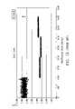
- FIG. 1A and FIG. 1Bshow an example of the wear for a non-volatile memory, e.g., a flash memory, in which every zone comprises 1,024 blocks (Block 0 to Block 1023 ), and Logical Block 0 of Zone 0 stores the File Allocation Table (FAT), which is updated whenever data is written to any zone.
- a non-volatile memorye.g., a flash memory
- every zonecomprises 1,024 blocks (Block 0 to Block 1023 )
- Logical Block 0 of Zone 0stores the File Allocation Table (FAT), which is updated whenever data is written to any zone.
- FATFile Allocation Table
- a physical blockis a fixed, physical address of a block of data on a non-volatile memory.
- a logical blockis the address that host or operating system uses it to read/write a block of data on a non-volatile memory.
- a logical blockis point to a physical block on a non-volatile memory which the operating system can use to read/write the data of the physical block.
- the File Allocation Table(FAT) is a partially patented file system developed by Microsoft for MS-DOS and was the primary file system for consumer versions of Microsoft Windows up to and including Windows Me.
- FATas it applies to flexible/floppy and optical disk cartridges (FAT12 and FAT16 without long file name support) has been standardized as ECMA-107 and ISO/IEC 9293.
- the FAT file systemis relatively uncomplicated, and is supported by virtually all existing operating systems for personal computers.
- the erase countis generally between 6,000 and 7,000.
- the erase countis around 3,300 to 3,500.
- the erase countis around 3,000 to 3,400.
- the erase countis around 3,600 to 3,800.
- Zone 0Because Logical Block 0 in Zone 0 usually stores the FAT, it can be seen that the erase (wear) occurs more often in Zone 0 than in other Zones. Therefore, although Zone 0 also performs wear leveling, the high wear rate caused by the FAT increases the average wear count in Zone 0 more rapidly than in other zones.
- the present inventionprovides a method of wear leveling for a non-volatile memory, by which the logical blocks of a zone having higher writing hit rates will change the pointer thereof to aim to some free physical blocks in other zones, so that the wear in all zones can be equalized and the endurance of the non-volatile memory can be increased.
- the non-volatile memoryis divided into a plurality of zones including at least a first zone, e.g., Zone 0 , and a second zone, e.g., Zone 1 .
- the first zoneis subjected to wear, i.e., written and/or erased, in which at least one first physical block mapped by an logical block having higher writing hit rate is written and/or erased more often and therefore resulting in higher writing and/or erasing count in the first zone.
- the logical block having higher writing hit ratemay store the file allocation table (FAT).
- the next sequential stepis to find a free second physical block in the second zone.
- the first physical block in the first zoneis replaced by the second physical block in the second zone when the write and/or erase count of the first zone exceeds a threshold number.
- the replacement of the first physical block by the second physical blockmay include the steps of copying the data of the first physical block in the first zone to the second physical block in the second zone, and changing the logical block originally pointing to the first physical block to point to the second physical block. As such, when writing or erasing again, the FAT in the second block will be updated.
- the present applicationis not limited to one block replacement; plural blocks in a zone can be replaced by other blocks in the same zone or different zones for flexibility consideration.
- FIG. 1Aillustrates the relation between physical block address and erase count of a prior art
- FIG. 1Billustrates the FAT location in a zone in accordance with the prior art
- FIG. 2Aillustrates an example of the relation between physical block address and erase count in accordance with the present invention
- FIG. 2Billustrates an example of block replacement of the method of wear leveling for a non-volatile memory in accordance with the present invention.
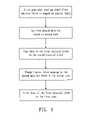
- FIG. 3illustrates a flow chart of the method of wear leveling for a non-volatile memory in accordance with the present invention.
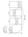
- a non-volatile memorysuch as a flash memory is divided into four zones including Zone 0 , Zone 1 , Zone 2 and Zone 3 .
- Each zoneincludes 1,024 physical blocks (Block 0 to Block 1023 ), and thus there are in total 4,096 blocks in the non-volatile memory.
- Zone 0e.g., table establishment between logical blocks and physical blocks
- Zone 1is scanned concurrently so as to find a free Physical Block A for later block replacement.
- Logical Block 0is selected but not limited to be exemplified below. If the Logical Block 0 directs to Physical Block X in Zone 0 when the number of write and/or erase in Zone 0 exceeds a threshold number, the data in Physical Block X of Zone 0 is copied to the selected Physical Block A in Zone 1 . Next, the data in Block X of Zone 0 is deleted, and the Logical Block 0 originally pointing to Block X is changed to point to Block A. In other words, Block X is replaced by Block A. The pointer of the logical block address Logical Block 0 pointing to Block A is recorded for later use.
- Block A's copy of Block X in Zone 1can be directed.
- the pointerwill switch from Zone 0 to Zone 1 . If the number of write to Zone 1 exceeds a threshold number, the data of Block A is copied to Block B in Zone 2 , and the data in Block A in Zone 1 is deleted. Next, the zone pointed to by Logical Block 0 is recorded. Likewise, a similar replacement can be implemented between Block B in Zone 2 and a free Block C in Zone 3 .
- the steps of finding a free block in another zone and the block replacement mentioned abovecan be repeated. As such, the wear count for Zone 0 can be significantly decreased, and the wear between zones can be equalized.
- the method of wear leveling for a non-volatile memorycan be illustrated in the flow chart shown in FIG. 3 .
- wear leveling for a first zonein which a first physical block is mapped by an logical block having higher writing hit rate, a free second physical block is obtained in a second zone.
- the first physical blockis replaced by the second physical block if the number of write and/or erase to the first zone exceeds a threshold number, in which the data in the first physical block is copied to the second physical block and the logical block is changed to be mapping to the second physical block.
- the data of the first physical block in the first zoneis erased.
- the present applicationis not limited to one block replacement; plural blocks in a zone can be replaced by other blocks in the same zone or different zones as well.
- three blocks in Zone 0can be replaced by three blocks in Zone 1 .
- the three blocks in Zone 1can be replaced by three blocks in Zone 2 , and the three blocks in Zone 2 can be replaced by three blocks in Zone 3 afterwards.
Landscapes
- Engineering & Computer Science (AREA)
- Theoretical Computer Science (AREA)
- Physics & Mathematics (AREA)
- General Engineering & Computer Science (AREA)
- General Physics & Mathematics (AREA)
- Techniques For Improving Reliability Of Storages (AREA)
- Information Retrieval, Db Structures And Fs Structures Therefor (AREA)
Abstract
Description
- (A) Field of the Invention
- The present invention is related to a method of wear leveling for a non-volatile memory.
- (B) Description of Related Art
- Wear leveling technology usually divides a non-volatile memory into a plurality of zones for recording in consideration of the limitation of RAM size, and every single zone usually contains a plurality of blocks. For wear leveling to blocks on the zone base, the blocks are worn uniformly in a zone, but normally the wear in different zones is not equal.
FIG. 1A andFIG. 1B show an example of the wear for a non-volatile memory, e.g., a flash memory, in which every zone comprises 1,024 blocks (Block 0 to Block1023), andLogical Block 0 ofZone 0 stores the File Allocation Table (FAT), which is updated whenever data is written to any zone.- A physical block is a fixed, physical address of a block of data on a non-volatile memory. A logical block is the address that host or operating system uses it to read/write a block of data on a non-volatile memory. A logical block is point to a physical block on a non-volatile memory which the operating system can use to read/write the data of the physical block.
- The File Allocation Table (FAT) is a partially patented file system developed by Microsoft for MS-DOS and was the primary file system for consumer versions of Microsoft Windows up to and including Windows Me. FAT as it applies to flexible/floppy and optical disk cartridges (FAT12 and FAT16 without long file name support) has been standardized as ECMA-107 and ISO/IEC 9293. The FAT file system is relatively uncomplicated, and is supported by virtually all existing operating systems for personal computers.
- For
Zone 0, i.e.,Physical Block 0 toPhysical Block 1023, the erase count is generally between 6,000 and 7,000. ForZone 1, i.e., Physical Block1024 to Physical Block2047, the erase count is around 3,300 to 3,500. ForZone 2, i.e., Physical Block2048 to Physical Block3071, the erase count is around 3,000 to 3,400. ForZone 3, i.e., Physical Block3071 to Physical Block4095, the erase count is around 3,600 to 3,800. - Because
Logical Block 0 inZone 0 usually stores the FAT, it can be seen that the erase (wear) occurs more often inZone 0 than in other Zones. Therefore, althoughZone 0 also performs wear leveling, the high wear rate caused by the FAT increases the average wear count inZone 0 more rapidly than in other zones. - Therefore, it is useful to decrease the wear counts in the first Zone (Zone0), so that the wear in all Zones can be equalized. As a result, the endurance of the non-volatile memory can be increased.
- The present invention provides a method of wear leveling for a non-volatile memory, by which the logical blocks of a zone having higher writing hit rates will change the pointer thereof to aim to some free physical blocks in other zones, so that the wear in all zones can be equalized and the endurance of the non-volatile memory can be increased.
- According to the method of wear leveling for a non-volatile memory of the present invention, the non-volatile memory is divided into a plurality of zones including at least a first zone, e.g.,
Zone 0, and a second zone, e.g.,Zone 1. The first zone is subjected to wear, i.e., written and/or erased, in which at least one first physical block mapped by an logical block having higher writing hit rate is written and/or erased more often and therefore resulting in higher writing and/or erasing count in the first zone. For example, the logical block having higher writing hit rate may store the file allocation table (FAT). - The next sequential step is to find a free second physical block in the second zone. The first physical block in the first zone is replaced by the second physical block in the second zone when the write and/or erase count of the first zone exceeds a threshold number. In an embodiment, the replacement of the first physical block by the second physical block may include the steps of copying the data of the first physical block in the first zone to the second physical block in the second zone, and changing the logical block originally pointing to the first physical block to point to the second physical block. As such, when writing or erasing again, the FAT in the second block will be updated.
- In practice, the present application is not limited to one block replacement; plural blocks in a zone can be replaced by other blocks in the same zone or different zones for flexibility consideration.
FIG. 1A illustrates the relation between physical block address and erase count of a prior art;FIG. 1B illustrates the FAT location in a zone in accordance with the prior art;FIG. 2A illustrates an example of the relation between physical block address and erase count in accordance with the present invention;FIG. 2B illustrates an example of block replacement of the method of wear leveling for a non-volatile memory in accordance with the present invention; andFIG. 3 illustrates a flow chart of the method of wear leveling for a non-volatile memory in accordance with the present invention.- Embodiments of the present invention will now be described with reference to the accompanying drawings.
- Referring to
FIG. 2A andFIG. 2B , a non-volatile memory such as a flash memory is divided into fourzones including Zone 0,Zone 1,Zone 2 andZone 3. Each zone includes 1,024 physical blocks (Block 0 to Block1023), and thus there are in total 4,096 blocks in the non-volatile memory. - If the number of write and/or erase in a zone exceeds a threshold number, wear leveling between the zones is started. While the procedural data is being built in
Zone 0, e.g., table establishment between logical blocks and physical blocks,Zone 1 is scanned concurrently so as to find a free Physical Block A for later block replacement. - Because
Logical Block 0 storing FAT may have higher writing hit rate,Logical Block 0 is selected but not limited to be exemplified below. If theLogical Block 0 directs to Physical Block X inZone 0 when the number of write and/or erase inZone 0 exceeds a threshold number, the data in Physical Block X ofZone 0 is copied to the selected Physical Block A inZone 1. Next, the data in Block X ofZone 0 is deleted, and theLogical Block 0 originally pointing to Block X is changed to point to Block A. In other words, Block X is replaced by Block A. The pointer of the logical block addressLogical Block 0 pointing to Block A is recorded for later use. - When the copy of Block X to Block A is completed, a preliminary scan on
Zone 2 is started, and a free Block B is selected for later block replacement. - For accessing
Logical Block 0, according to the pointer ofLogical Block 0, Block A's copy of Block X inZone 1 can be directed. In other words, for accessingLogical Block 0, the pointer will switch fromZone 0 toZone 1. If the number of write toZone 1 exceeds a threshold number, the data of Block A is copied to Block B inZone 2, and the data in Block A inZone 1 is deleted. Next, the zone pointed to byLogical Block 0 is recorded. Likewise, a similar replacement can be implemented between Block B inZone 2 and a free Block C inZone 3. - In the period between the block replacements, other wear leveling is still performed in each zone. That is, blocks with high wear counts are replaced with blocks having low wear counts.
- The steps of finding a free block in another zone and the block replacement mentioned above can be repeated. As such, the wear count for
Zone 0 can be significantly decreased, and the wear between zones can be equalized. - In summary, the method of wear leveling for a non-volatile memory can be illustrated in the flow chart shown in
FIG. 3 . When wear leveling for a first zone is started, in which a first physical block is mapped by an logical block having higher writing hit rate, a free second physical block is obtained in a second zone. Then the first physical block is replaced by the second physical block if the number of write and/or erase to the first zone exceeds a threshold number, in which the data in the first physical block is copied to the second physical block and the logical block is changed to be mapping to the second physical block. Finally, the data of the first physical block in the first zone is erased. - In practice, the present application is not limited to one block replacement; plural blocks in a zone can be replaced by other blocks in the same zone or different zones as well. For instance, three blocks in
Zone 0 can be replaced by three blocks inZone 1. Likewise, the three blocks inZone 1 can be replaced by three blocks inZone 2, and the three blocks inZone 2 can be replaced by three blocks inZone 3 afterwards. - The above-described embodiments of the present invention are intended to be illustrative only. Numerous alternative embodiments may be devised by those skilled in the art without departing from the scope of the following claims.
Claims (13)
1. A method of wear leveling for a non-volatile memory, comprising the steps of:
providing a logical block having higher writing frequency, and the logical block pointing to a first physical block in a first zone of the non-volatile memory;
finding a second physical block that is free in a second zone of the non-volatile memory;
copying data of the first physical block in the first zone to the second physical block in the second zone; and
changing a mapping of the logical block to point to the second physical block in the second zone.
2. The method ofclaim 1 , wherein the step of copying data from the first physical block in the first zone to the second physical block in the second zone is performed when the number of write and/or erase to the first zone exceeds a threshold number.
3. The method ofclaim 2 , wherein data of the first physical block is erased after copying data of the first physical block in the first zone to the second physical block in the second zone.
4. The method ofclaim 1 , wherein the step of finding a second physical block is performed when rebuilding a table mapping logical blocks to physical blocks in the first zone.
5. The method ofclaim 2 , wherein the first or other zone can performs other wear leveling algorithm.
6. The method ofclaim 1 , wherein the logical block comprises the File Allocation Table (FAT).
7. A method of wear leveling for a non-volatile memory, comprising the steps of:
dividing the non-volatile memory into zones including at least a first zone and a second zone;
writing or erasing the first zone in which a logical block has higher writing or erasing count, the logical block pointing to a first physical block in the first zone;
finding a second physical block that is free in the second zone; and
replacing the first physical block by the second physical block when the number of write and/or erase to the first zone exceeds a threshold number.
8. The method ofclaim 7 , wherein the step of replacing the first physical block by the second physical block comprises:
copying data of the first physical block in the first zone to the second physical block in the second zone; and
changing a mapping of the logical block to point to the second physical block in the second zone.
9. The method ofclaim 8 , further comprising the step of erasing data of the first block after changing the logical block to point to the second physical block in the second zone.
10. The method ofclaim 7 , wherein the logical block comprises the File Allocation Table (FAT).
11. The method ofclaim 7 , wherein finding a second physical block is performed when rebuilding a table mapping logical blocks to physical blocks in the first zone.
12. The method ofclaim 7 , wherein the step of writing or erasing the first zone undergoes other wear leveling algorithm.
13. The method ofclaim 7 , wherein the second zone is next to the first zone.
Priority Applications (2)
| Application Number | Priority Date | Filing Date | Title |
|---|---|---|---|
| US12/100,136US20090259819A1 (en) | 2008-04-09 | 2008-04-09 | Method of wear leveling for non-volatile memory |
| TW097123016ATWI368846B (en) | 2008-04-09 | 2008-06-20 | Method of wear leveling for non-volatile memory |
Applications Claiming Priority (1)
| Application Number | Priority Date | Filing Date | Title |
|---|---|---|---|
| US12/100,136US20090259819A1 (en) | 2008-04-09 | 2008-04-09 | Method of wear leveling for non-volatile memory |
Publications (1)
| Publication Number | Publication Date |
|---|---|
| US20090259819A1true US20090259819A1 (en) | 2009-10-15 |
Family
ID=41164938
Family Applications (1)
| Application Number | Title | Priority Date | Filing Date |
|---|---|---|---|
| US12/100,136AbandonedUS20090259819A1 (en) | 2008-04-09 | 2008-04-09 | Method of wear leveling for non-volatile memory |
Country Status (2)
| Country | Link |
|---|---|
| US (1) | US20090259819A1 (en) |
| TW (1) | TWI368846B (en) |
Cited By (42)
| Publication number | Priority date | Publication date | Assignee | Title |
|---|---|---|---|---|
| US20090271567A1 (en)* | 2007-01-17 | 2009-10-29 | Memoright Memoritech (Shenzhen) Co., Ltd. | Methods for managing blocks in flash memories |
| US20100268865A1 (en)* | 2009-04-20 | 2010-10-21 | Arunprasad Ramiya Mothilal | Static Wear Leveling |
| US20100268864A1 (en)* | 2009-04-20 | 2010-10-21 | Arunprasad Ramiya Mothilal | Logical-to-Physical Address Translation for a Removable Data Storage Device |
| US20120203993A1 (en)* | 2011-02-08 | 2012-08-09 | SMART Storage Systems, Inc. | Memory system with tiered queuing and method of operation thereof |
| US8539139B1 (en)* | 2010-12-17 | 2013-09-17 | Teradota Us, Inc. | Managing device wearout using I/O metering |
| US8601202B1 (en)* | 2009-08-26 | 2013-12-03 | Micron Technology, Inc. | Full chip wear leveling in memory device |
| US8699175B1 (en)* | 2012-07-20 | 2014-04-15 | Western Digital Technologies, Inc. | Disk drive mapping low frequency write addresses to circular buffer write zone |
| US20140173234A1 (en)* | 2012-12-13 | 2014-06-19 | Samsung Electronics Co., Ltd. | Semiconductor memory device and memory system |
| CN104156317A (en)* | 2014-08-08 | 2014-11-19 | 浪潮(北京)电子信息产业有限公司 | Wiping and writing management method and system for non-volatile flash memory |
| US8909851B2 (en) | 2011-02-08 | 2014-12-09 | SMART Storage Systems, Inc. | Storage control system with change logging mechanism and method of operation thereof |
| US8935466B2 (en) | 2011-03-28 | 2015-01-13 | SMART Storage Systems, Inc. | Data storage system with non-volatile memory and method of operation thereof |
| US8949689B2 (en) | 2012-06-11 | 2015-02-03 | SMART Storage Systems, Inc. | Storage control system with data management mechanism and method of operation thereof |
| US9021319B2 (en) | 2011-09-02 | 2015-04-28 | SMART Storage Systems, Inc. | Non-volatile memory management system with load leveling and method of operation thereof |
| US9021231B2 (en) | 2011-09-02 | 2015-04-28 | SMART Storage Systems, Inc. | Storage control system with write amplification control mechanism and method of operation thereof |
| US9043780B2 (en) | 2013-03-27 | 2015-05-26 | SMART Storage Systems, Inc. | Electronic system with system modification control mechanism and method of operation thereof |
| US9063844B2 (en) | 2011-09-02 | 2015-06-23 | SMART Storage Systems, Inc. | Non-volatile memory management system with time measure mechanism and method of operation thereof |
| US9098399B2 (en) | 2011-08-31 | 2015-08-04 | SMART Storage Systems, Inc. | Electronic system with storage management mechanism and method of operation thereof |
| US9123445B2 (en) | 2013-01-22 | 2015-09-01 | SMART Storage Systems, Inc. | Storage control system with data management mechanism and method of operation thereof |
| US9129628B1 (en) | 2014-10-23 | 2015-09-08 | Western Digital Technologies, Inc. | Data management for data storage device with different track density regions |
| US9146850B2 (en) | 2013-08-01 | 2015-09-29 | SMART Storage Systems, Inc. | Data storage system with dynamic read threshold mechanism and method of operation thereof |
| US9152555B2 (en) | 2013-11-15 | 2015-10-06 | Sandisk Enterprise IP LLC. | Data management with modular erase in a data storage system |
| US9170941B2 (en) | 2013-04-05 | 2015-10-27 | Sandisk Enterprises IP LLC | Data hardening in a storage system |
| US9183137B2 (en) | 2013-02-27 | 2015-11-10 | SMART Storage Systems, Inc. | Storage control system with data management mechanism and method of operation thereof |
| US9214965B2 (en) | 2013-02-20 | 2015-12-15 | Sandisk Enterprise Ip Llc | Method and system for improving data integrity in non-volatile storage |
| US9239781B2 (en) | 2012-02-07 | 2016-01-19 | SMART Storage Systems, Inc. | Storage control system with erase block mechanism and method of operation thereof |
| US9244519B1 (en) | 2013-06-25 | 2016-01-26 | Smart Storage Systems. Inc. | Storage system with data transfer rate adjustment for power throttling |
| US9313874B2 (en) | 2013-06-19 | 2016-04-12 | SMART Storage Systems, Inc. | Electronic system with heat extraction and method of manufacture thereof |
| US9329928B2 (en) | 2013-02-20 | 2016-05-03 | Sandisk Enterprise IP LLC. | Bandwidth optimization in a non-volatile memory system |
| US9361222B2 (en) | 2013-08-07 | 2016-06-07 | SMART Storage Systems, Inc. | Electronic system with storage drive life estimation mechanism and method of operation thereof |
| US9367353B1 (en) | 2013-06-25 | 2016-06-14 | Sandisk Technologies Inc. | Storage control system with power throttling mechanism and method of operation thereof |
| US9431113B2 (en) | 2013-08-07 | 2016-08-30 | Sandisk Technologies Llc | Data storage system with dynamic erase block grouping mechanism and method of operation thereof |
| US9448946B2 (en) | 2013-08-07 | 2016-09-20 | Sandisk Technologies Llc | Data storage system with stale data mechanism and method of operation thereof |
| US9470720B2 (en) | 2013-03-08 | 2016-10-18 | Sandisk Technologies Llc | Test system with localized heating and method of manufacture thereof |
| US9543025B2 (en) | 2013-04-11 | 2017-01-10 | Sandisk Technologies Llc | Storage control system with power-off time estimation mechanism and method of operation thereof |
| US9671962B2 (en) | 2012-11-30 | 2017-06-06 | Sandisk Technologies Llc | Storage control system with data management mechanism of parity and method of operation thereof |
| US9898056B2 (en) | 2013-06-19 | 2018-02-20 | Sandisk Technologies Llc | Electronic assembly with thermal channel and method of manufacture thereof |
| WO2018089084A1 (en)* | 2016-11-08 | 2018-05-17 | Micron Technology, Inc. | Memory operations on data |
| US10049037B2 (en) | 2013-04-05 | 2018-08-14 | Sandisk Enterprise Ip Llc | Data management in a storage system |
| US20180268913A1 (en)* | 2015-09-30 | 2018-09-20 | Hewlett Packard Enterprise Development Lp | Remapping operations |
| CN110175385A (en)* | 2019-05-20 | 2019-08-27 | 山东大学 | A kind of non-volatile FPGA layout optimization method and system based on performance abrasion equilibrium |
| US10546648B2 (en) | 2013-04-12 | 2020-01-28 | Sandisk Technologies Llc | Storage control system with data management mechanism and method of operation thereof |
| US10956290B2 (en) | 2016-11-08 | 2021-03-23 | Micron Technology, Inc. | Memory management |
Families Citing this family (1)
| Publication number | Priority date | Publication date | Assignee | Title |
|---|---|---|---|---|
| CN103645991B (en)* | 2013-11-22 | 2017-02-15 | 华为技术有限公司 | Data processing method and device |
Citations (6)
| Publication number | Priority date | Publication date | Assignee | Title |
|---|---|---|---|---|
| US5479638A (en)* | 1993-03-26 | 1995-12-26 | Cirrus Logic, Inc. | Flash memory mass storage architecture incorporation wear leveling technique |
| US20030227804A1 (en)* | 1991-09-13 | 2003-12-11 | Sandisk Corporation And Western Digital Corporation | Wear leveling techniques for flash EEPROM systems |
| US20040083335A1 (en)* | 2002-10-28 | 2004-04-29 | Gonzalez Carlos J. | Automated wear leveling in non-volatile storage systems |
| US6985992B1 (en)* | 2002-10-28 | 2006-01-10 | Sandisk Corporation | Wear-leveling in non-volatile storage systems |
| US20070050536A1 (en)* | 2005-09-01 | 2007-03-01 | Cypress Semiconductor Corporation | Flash drive fast wear leveling |
| US7224604B2 (en)* | 2005-03-14 | 2007-05-29 | Sandisk Il Ltd. | Method of achieving wear leveling in flash memory using relative grades |
- 2008
- 2008-04-09USUS12/100,136patent/US20090259819A1/ennot_activeAbandoned
- 2008-06-20TWTW097123016Apatent/TWI368846B/ennot_activeIP Right Cessation
Patent Citations (6)
| Publication number | Priority date | Publication date | Assignee | Title |
|---|---|---|---|---|
| US20030227804A1 (en)* | 1991-09-13 | 2003-12-11 | Sandisk Corporation And Western Digital Corporation | Wear leveling techniques for flash EEPROM systems |
| US5479638A (en)* | 1993-03-26 | 1995-12-26 | Cirrus Logic, Inc. | Flash memory mass storage architecture incorporation wear leveling technique |
| US20040083335A1 (en)* | 2002-10-28 | 2004-04-29 | Gonzalez Carlos J. | Automated wear leveling in non-volatile storage systems |
| US6985992B1 (en)* | 2002-10-28 | 2006-01-10 | Sandisk Corporation | Wear-leveling in non-volatile storage systems |
| US7224604B2 (en)* | 2005-03-14 | 2007-05-29 | Sandisk Il Ltd. | Method of achieving wear leveling in flash memory using relative grades |
| US20070050536A1 (en)* | 2005-09-01 | 2007-03-01 | Cypress Semiconductor Corporation | Flash drive fast wear leveling |
Non-Patent Citations (1)
| Title |
|---|
| Kim et al., A SPACE-EFFICIENT FLASH TRANSLATION LAYER FOR COMPACTFLASH SYSTEMS, IEEE Transactions on Consumer Electronics, Vol. 48, No. 2, MAY 2002* |
Cited By (58)
| Publication number | Priority date | Publication date | Assignee | Title |
|---|---|---|---|---|
| US8122184B2 (en)* | 2007-01-17 | 2012-02-21 | Memoright Memoritech (Wuhan) Co., Ltd. | Methods for managing blocks in flash memories |
| US20090271567A1 (en)* | 2007-01-17 | 2009-10-29 | Memoright Memoritech (Shenzhen) Co., Ltd. | Methods for managing blocks in flash memories |
| US8510532B2 (en) | 2009-04-20 | 2013-08-13 | Imation Corp. | Logical-to-physical address translation for a removable data storage device |
| US8725985B2 (en) | 2009-04-20 | 2014-05-13 | Imation Corp. | Logical-to-physical address translation for a removable data storage device |
| US20100268864A1 (en)* | 2009-04-20 | 2010-10-21 | Arunprasad Ramiya Mothilal | Logical-to-Physical Address Translation for a Removable Data Storage Device |
| US8176295B2 (en) | 2009-04-20 | 2012-05-08 | Imation Corp. | Logical-to-physical address translation for a removable data storage device |
| US9520992B2 (en) | 2009-04-20 | 2016-12-13 | Kingston Digital, Inc. | Logical-to-physical address translation for a removable data storage device |
| US8407408B2 (en) | 2009-04-20 | 2013-03-26 | Imation Corp. | Static wear leveling |
| US9286243B2 (en) | 2009-04-20 | 2016-03-15 | Imation Corp. | Logical-to-physical address translation for a removable data storage device |
| US8065469B2 (en)* | 2009-04-20 | 2011-11-22 | Imation Corp. | Static wear leveling |
| US20100268865A1 (en)* | 2009-04-20 | 2010-10-21 | Arunprasad Ramiya Mothilal | Static Wear Leveling |
| US8601202B1 (en)* | 2009-08-26 | 2013-12-03 | Micron Technology, Inc. | Full chip wear leveling in memory device |
| US8539139B1 (en)* | 2010-12-17 | 2013-09-17 | Teradota Us, Inc. | Managing device wearout using I/O metering |
| US20120203993A1 (en)* | 2011-02-08 | 2012-08-09 | SMART Storage Systems, Inc. | Memory system with tiered queuing and method of operation thereof |
| US8909851B2 (en) | 2011-02-08 | 2014-12-09 | SMART Storage Systems, Inc. | Storage control system with change logging mechanism and method of operation thereof |
| US8935466B2 (en) | 2011-03-28 | 2015-01-13 | SMART Storage Systems, Inc. | Data storage system with non-volatile memory and method of operation thereof |
| US9098399B2 (en) | 2011-08-31 | 2015-08-04 | SMART Storage Systems, Inc. | Electronic system with storage management mechanism and method of operation thereof |
| US9063844B2 (en) | 2011-09-02 | 2015-06-23 | SMART Storage Systems, Inc. | Non-volatile memory management system with time measure mechanism and method of operation thereof |
| US9021319B2 (en) | 2011-09-02 | 2015-04-28 | SMART Storage Systems, Inc. | Non-volatile memory management system with load leveling and method of operation thereof |
| US9021231B2 (en) | 2011-09-02 | 2015-04-28 | SMART Storage Systems, Inc. | Storage control system with write amplification control mechanism and method of operation thereof |
| US9239781B2 (en) | 2012-02-07 | 2016-01-19 | SMART Storage Systems, Inc. | Storage control system with erase block mechanism and method of operation thereof |
| US8949689B2 (en) | 2012-06-11 | 2015-02-03 | SMART Storage Systems, Inc. | Storage control system with data management mechanism and method of operation thereof |
| US8699175B1 (en)* | 2012-07-20 | 2014-04-15 | Western Digital Technologies, Inc. | Disk drive mapping low frequency write addresses to circular buffer write zone |
| US9671962B2 (en) | 2012-11-30 | 2017-06-06 | Sandisk Technologies Llc | Storage control system with data management mechanism of parity and method of operation thereof |
| US9772803B2 (en)* | 2012-12-13 | 2017-09-26 | Samsung Electronics Co., Ltd. | Semiconductor memory device and memory system |
| US20140173234A1 (en)* | 2012-12-13 | 2014-06-19 | Samsung Electronics Co., Ltd. | Semiconductor memory device and memory system |
| US9123445B2 (en) | 2013-01-22 | 2015-09-01 | SMART Storage Systems, Inc. | Storage control system with data management mechanism and method of operation thereof |
| US9214965B2 (en) | 2013-02-20 | 2015-12-15 | Sandisk Enterprise Ip Llc | Method and system for improving data integrity in non-volatile storage |
| US9329928B2 (en) | 2013-02-20 | 2016-05-03 | Sandisk Enterprise IP LLC. | Bandwidth optimization in a non-volatile memory system |
| US9183137B2 (en) | 2013-02-27 | 2015-11-10 | SMART Storage Systems, Inc. | Storage control system with data management mechanism and method of operation thereof |
| US9470720B2 (en) | 2013-03-08 | 2016-10-18 | Sandisk Technologies Llc | Test system with localized heating and method of manufacture thereof |
| US9043780B2 (en) | 2013-03-27 | 2015-05-26 | SMART Storage Systems, Inc. | Electronic system with system modification control mechanism and method of operation thereof |
| US9170941B2 (en) | 2013-04-05 | 2015-10-27 | Sandisk Enterprises IP LLC | Data hardening in a storage system |
| US10049037B2 (en) | 2013-04-05 | 2018-08-14 | Sandisk Enterprise Ip Llc | Data management in a storage system |
| US9543025B2 (en) | 2013-04-11 | 2017-01-10 | Sandisk Technologies Llc | Storage control system with power-off time estimation mechanism and method of operation thereof |
| US10546648B2 (en) | 2013-04-12 | 2020-01-28 | Sandisk Technologies Llc | Storage control system with data management mechanism and method of operation thereof |
| US9898056B2 (en) | 2013-06-19 | 2018-02-20 | Sandisk Technologies Llc | Electronic assembly with thermal channel and method of manufacture thereof |
| US9313874B2 (en) | 2013-06-19 | 2016-04-12 | SMART Storage Systems, Inc. | Electronic system with heat extraction and method of manufacture thereof |
| US9244519B1 (en) | 2013-06-25 | 2016-01-26 | Smart Storage Systems. Inc. | Storage system with data transfer rate adjustment for power throttling |
| US9367353B1 (en) | 2013-06-25 | 2016-06-14 | Sandisk Technologies Inc. | Storage control system with power throttling mechanism and method of operation thereof |
| US9146850B2 (en) | 2013-08-01 | 2015-09-29 | SMART Storage Systems, Inc. | Data storage system with dynamic read threshold mechanism and method of operation thereof |
| US9448946B2 (en) | 2013-08-07 | 2016-09-20 | Sandisk Technologies Llc | Data storage system with stale data mechanism and method of operation thereof |
| US9665295B2 (en) | 2013-08-07 | 2017-05-30 | Sandisk Technologies Llc | Data storage system with dynamic erase block grouping mechanism and method of operation thereof |
| US9431113B2 (en) | 2013-08-07 | 2016-08-30 | Sandisk Technologies Llc | Data storage system with dynamic erase block grouping mechanism and method of operation thereof |
| US9361222B2 (en) | 2013-08-07 | 2016-06-07 | SMART Storage Systems, Inc. | Electronic system with storage drive life estimation mechanism and method of operation thereof |
| US9152555B2 (en) | 2013-11-15 | 2015-10-06 | Sandisk Enterprise IP LLC. | Data management with modular erase in a data storage system |
| CN104156317A (en)* | 2014-08-08 | 2014-11-19 | 浪潮(北京)电子信息产业有限公司 | Wiping and writing management method and system for non-volatile flash memory |
| US9129628B1 (en) | 2014-10-23 | 2015-09-08 | Western Digital Technologies, Inc. | Data management for data storage device with different track density regions |
| US20180268913A1 (en)* | 2015-09-30 | 2018-09-20 | Hewlett Packard Enterprise Development Lp | Remapping operations |
| US10847235B2 (en)* | 2015-09-30 | 2020-11-24 | Hewlett Packard Enterprise Development Lp | Remapping operations |
| WO2018089084A1 (en)* | 2016-11-08 | 2018-05-17 | Micron Technology, Inc. | Memory operations on data |
| CN109923514A (en)* | 2016-11-08 | 2019-06-21 | 美光科技公司 | Memory operation on data |
| US10430085B2 (en) | 2016-11-08 | 2019-10-01 | Micron Technology, Inc. | Memory operations on data |
| US10956290B2 (en) | 2016-11-08 | 2021-03-23 | Micron Technology, Inc. | Memory management |
| US11209986B2 (en) | 2016-11-08 | 2021-12-28 | Micron Technology, Inc. | Memory operations on data |
| US11550678B2 (en) | 2016-11-08 | 2023-01-10 | Micron Technology, Inc. | Memory management |
| US11886710B2 (en) | 2016-11-08 | 2024-01-30 | Micron Technology, Inc. | Memory operations on data |
| CN110175385A (en)* | 2019-05-20 | 2019-08-27 | 山东大学 | A kind of non-volatile FPGA layout optimization method and system based on performance abrasion equilibrium |
Also Published As
| Publication number | Publication date |
|---|---|
| TWI368846B (en) | 2012-07-21 |
| TW200943059A (en) | 2009-10-16 |
Similar Documents
| Publication | Publication Date | Title |
|---|---|---|
| US20090259819A1 (en) | Method of wear leveling for non-volatile memory | |
| US20110238892A1 (en) | Wear leveling method of non-volatile memory | |
| US8832371B2 (en) | Storage system with multiple flash memory packages and data control method therefor | |
| US9753847B2 (en) | Non-volatile semiconductor memory segregating sequential, random, and system data to reduce garbage collection for page based mapping | |
| US7747813B2 (en) | Multi-memory device system and method for managing a lifetime thereof | |
| US9690695B2 (en) | Data storage device and flash memory control method thereof | |
| US7809900B2 (en) | System, method, and computer program product for delaying an operation that reduces a lifetime of memory | |
| CN109656486B (en) | Configuration method of solid state disk, data storage method, solid state disk and storage controller | |
| EP2319047B1 (en) | Multiple performance mode memory system | |
| EP2631916B1 (en) | Data deletion method and apparatus | |
| US8316176B1 (en) | Non-volatile semiconductor memory segregating sequential data during garbage collection to reduce write amplification | |
| US8671233B2 (en) | Techniques for reducing memory write operations using coalescing memory buffers and difference information | |
| US7634624B2 (en) | Memory system for data storage and retrieval | |
| US8392647B2 (en) | Solid state storage system for controlling reserved area flexibly and method for controlling the same | |
| US20080307164A1 (en) | Method And System For Memory Block Flushing | |
| US8370680B2 (en) | Solid state storage system for controlling reserved area and method of controlling the same | |
| US20080126891A1 (en) | Memory lifetime gauging system, method and computer program product | |
| US20100169556A1 (en) | Nonvolatile storage device, information recording system, and information recording method | |
| US20130326169A1 (en) | Method and Storage Device for Detection of Streaming Data Based on Logged Read/Write Transactions | |
| US8271721B2 (en) | Data writing method and data storage device | |
| US20100180072A1 (en) | Memory controller, nonvolatile memory device, file system, nonvolatile memory system, data writing method and data writing program | |
| CN104007939A (en) | Embedded FAT file system and method for frequently writing small files | |
| US11256432B2 (en) | Memory controller and memory system | |
| US8762623B2 (en) | Method for managing a plurality of blocks of a flash memory, and associated memory device and controller thereof | |
| US8209487B2 (en) | Block update for flash memory utilizing a cache page and cache block |
Legal Events
| Date | Code | Title | Description |
|---|---|---|---|
| AS | Assignment | Owner name:SKYMEDI CORPORATION, TAIWAN Free format text:ASSIGNMENT OF ASSIGNORS INTEREST;ASSIGNORS:CHEN, YEN MING;TAI, SHIH CHIEH;JI, YUNG LI;AND OTHERS;REEL/FRAME:020778/0574 Effective date:20080213 | |
| STCB | Information on status: application discontinuation | Free format text:ABANDONED -- FAILURE TO RESPOND TO AN OFFICE ACTION |