US20090257170A1 - Method for Forming a Ruthenium Film - Google Patents
Method for Forming a Ruthenium FilmDownload PDFInfo
- Publication number
- US20090257170A1 US20090257170A1US12/100,632US10063208AUS2009257170A1US 20090257170 A1US20090257170 A1US 20090257170A1US 10063208 AUS10063208 AUS 10063208AUS 2009257170 A1US2009257170 A1US 2009257170A1
- Authority
- US
- United States
- Prior art keywords
- ruthenium
- layer
- silicon
- forming
- substrate
- Prior art date
- Legal status (The legal status is an assumption and is not a legal conclusion. Google has not performed a legal analysis and makes no representation as to the accuracy of the status listed.)
- Granted
Links
- KJTLSVCANCCWHF-UHFFFAOYSA-NRutheniumChemical compound[Ru]KJTLSVCANCCWHF-UHFFFAOYSA-N0.000titleclaimsabstractdescription153
- 229910052707rutheniumInorganic materials0.000titleclaimsabstractdescription151
- 238000000034methodMethods0.000titleclaimsabstractdescription48
- 239000003990capacitorSubstances0.000claimsabstractdescription12
- 239000004065semiconductorSubstances0.000claimsabstractdescription10
- 239000010410layerSubstances0.000claimsdescription144
- 239000002243precursorSubstances0.000claimsdescription40
- 229910052710siliconInorganic materials0.000claimsdescription39
- 239000000758substrateSubstances0.000claimsdescription39
- XUIMIQQOPSSXEZ-UHFFFAOYSA-NSiliconChemical compound[Si]XUIMIQQOPSSXEZ-UHFFFAOYSA-N0.000claimsdescription38
- 229910052739hydrogenInorganic materials0.000claimsdescription38
- 239000010703siliconSubstances0.000claimsdescription38
- UFHFLCQGNIYNRP-UHFFFAOYSA-NHydrogenChemical compound[H][H]UFHFLCQGNIYNRP-UHFFFAOYSA-N0.000claimsdescription37
- 239000007789gasSubstances0.000claimsdescription36
- 239000001257hydrogenSubstances0.000claimsdescription36
- 239000000463materialSubstances0.000claimsdescription21
- 230000006911nucleationEffects0.000claimsdescription17
- 238000010899nucleationMethods0.000claimsdescription17
- 239000003989dielectric materialSubstances0.000claimsdescription16
- 239000012686silicon precursorSubstances0.000claimsdescription14
- 238000005229chemical vapour depositionMethods0.000claimsdescription13
- 238000000151depositionMethods0.000claimsdescription13
- BPUBBGLMJRNUCC-UHFFFAOYSA-Noxygen(2-);tantalum(5+)Chemical compound[O-2].[O-2].[O-2].[O-2].[O-2].[Ta+5].[Ta+5]BPUBBGLMJRNUCC-UHFFFAOYSA-N0.000claimsdescription11
- 229910001936tantalum oxideInorganic materials0.000claimsdescription11
- 238000012545processingMethods0.000claimsdescription9
- 230000015654memoryEffects0.000claimsdescription7
- 238000009792diffusion processMethods0.000claimsdescription6
- 238000004519manufacturing processMethods0.000claimsdescription5
- 229910021332silicideInorganic materials0.000claimsdescription5
- FVBUAEGBCNSCDD-UHFFFAOYSA-Nsilicide(4-)Chemical compound[Si-4]FVBUAEGBCNSCDD-UHFFFAOYSA-N0.000claimsdescription5
- 230000003247decreasing effectEffects0.000claimsdescription4
- 239000005380borophosphosilicate glassSubstances0.000claimsdescription3
- 238000004891communicationMethods0.000claimsdescription3
- 239000004020conductorSubstances0.000claimsdescription3
- 239000005360phosphosilicate glassSubstances0.000claimsdescription3
- 238000005240physical vapour depositionMethods0.000claimsdescription3
- 229910052581Si3N4Inorganic materials0.000claimsdescription2
- 239000002356single layerSubstances0.000claimsdescription2
- PNXKRHWROOZWSO-UHFFFAOYSA-N[Si].[Ru]Chemical compound[Si].[Ru]PNXKRHWROOZWSO-UHFFFAOYSA-N0.000claims1
- 230000004888barrier functionEffects0.000claims1
- HQVNEWCFYHHQES-UHFFFAOYSA-Nsilicon nitrideChemical compoundN12[Si]34N5[Si]62N3[Si]51N64HQVNEWCFYHHQES-UHFFFAOYSA-N0.000claims1
- 239000002210silicon-based materialSubstances0.000claims1
- 239000000126substanceSubstances0.000claims1
- 235000012431wafersNutrition0.000description9
- VYPSYNLAJGMNEJ-UHFFFAOYSA-NSilicium dioxideChemical compoundO=[Si]=OVYPSYNLAJGMNEJ-UHFFFAOYSA-N0.000description6
- 239000012159carrier gasSubstances0.000description6
- 238000006243chemical reactionMethods0.000description6
- 230000008021depositionEffects0.000description6
- QGZKDVFQNNGYKY-UHFFFAOYSA-NAmmoniaChemical compoundNQGZKDVFQNNGYKY-UHFFFAOYSA-N0.000description4
- XKRFYHLGVUSROY-UHFFFAOYSA-NArgonChemical compound[Ar]XKRFYHLGVUSROY-UHFFFAOYSA-N0.000description4
- IJGRMHOSHXDMSA-UHFFFAOYSA-NAtomic nitrogenChemical compoundN#NIJGRMHOSHXDMSA-UHFFFAOYSA-N0.000description4
- 229910052786argonInorganic materials0.000description4
- 230000006870functionEffects0.000description4
- 229910052734heliumInorganic materials0.000description4
- -1silane (SiH4)Chemical compound0.000description4
- 125000006527(C1-C5) alkyl groupChemical group0.000description3
- BLRPTPMANUNPDV-UHFFFAOYSA-NSilaneChemical compound[SiH4]BLRPTPMANUNPDV-UHFFFAOYSA-N0.000description3
- 238000004833X-ray photoelectron spectroscopyMethods0.000description3
- 230000015572biosynthetic processEffects0.000description3
- UOCJDOLVGGIYIQ-PBFPGSCMSA-NcefatrizineChemical groupS([C@@H]1[C@@H](C(N1C=1C(O)=O)=O)NC(=O)[C@H](N)C=2C=CC(O)=CC=2)CC=1CSC=1C=NNN=1UOCJDOLVGGIYIQ-PBFPGSCMSA-N0.000description3
- 150000001993dienesChemical class0.000description3
- 238000005755formation reactionMethods0.000description3
- 239000012634fragmentSubstances0.000description3
- 125000001449isopropyl groupChemical group[H]C([H])([H])C([H])(*)C([H])([H])[H]0.000description3
- 125000004108n-butyl groupChemical group[H]C([H])([H])C([H])([H])C([H])([H])C([H])([H])*0.000description3
- 125000004123n-propyl groupChemical group[H]C([H])([H])C([H])([H])C([H])([H])*0.000description3
- 229910052757nitrogenInorganic materials0.000description3
- 238000001004secondary ion mass spectrometryMethods0.000description3
- 239000000377silicon dioxideSubstances0.000description3
- 230000001360synchronised effectEffects0.000description3
- 125000000999tert-butyl groupChemical group[H]C([H])([H])C(*)(C([H])([H])[H])C([H])([H])[H]0.000description3
- 229910020294Pb(Zr,Ti)O3Inorganic materials0.000description2
- 0[1*]c1c([2*])c([3*])c([4*])c1[5*]Chemical compound[1*]c1c([2*])c([3*])c([4*])c1[5*]0.000description2
- 238000004458analytical methodMethods0.000description2
- 230000000712assemblyEffects0.000description2
- 238000000429assemblyMethods0.000description2
- 238000001505atmospheric-pressure chemical vapour depositionMethods0.000description2
- 238000000231atomic layer depositionMethods0.000description2
- 229910052454barium strontium titanateInorganic materials0.000description2
- NQZFAUXPNWSLBI-UHFFFAOYSA-Ncarbon monoxide;rutheniumChemical group[Ru].[Ru].[Ru].[O+]#[C-].[O+]#[C-].[O+]#[C-].[O+]#[C-].[O+]#[C-].[O+]#[C-].[O+]#[C-].[O+]#[C-].[O+]#[C-].[O+]#[C-].[O+]#[C-].[O+]#[C-]NQZFAUXPNWSLBI-UHFFFAOYSA-N0.000description2
- 238000010276constructionMethods0.000description2
- 238000007796conventional methodMethods0.000description2
- 238000010586diagramMethods0.000description2
- PZPGRFITIJYNEJ-UHFFFAOYSA-NdisilaneChemical compound[SiH3][SiH3]PZPGRFITIJYNEJ-UHFFFAOYSA-N0.000description2
- 238000005516engineering processMethods0.000description2
- 239000008246gaseous mixtureSubstances0.000description2
- 239000001307heliumSubstances0.000description2
- SWQJXJOGLNCZEY-UHFFFAOYSA-Nhelium atomChemical compound[He]SWQJXJOGLNCZEY-UHFFFAOYSA-N0.000description2
- 238000010348incorporationMethods0.000description2
- 239000011261inert gasSubstances0.000description2
- 229910052746lanthanumInorganic materials0.000description2
- 239000007788liquidSubstances0.000description2
- 238000004518low pressure chemical vapour depositionMethods0.000description2
- 229910044991metal oxideInorganic materials0.000description2
- 150000004706metal oxidesChemical class0.000description2
- 229910052754neonInorganic materials0.000description2
- GKAOGPIIYCISHV-UHFFFAOYSA-Nneon atomChemical compound[Ne]GKAOGPIIYCISHV-UHFFFAOYSA-N0.000description2
- 229910000069nitrogen hydrideInorganic materials0.000description2
- 238000000623plasma-assisted chemical vapour depositionMethods0.000description2
- BASFCYQUMIYNBI-UHFFFAOYSA-NplatinumChemical compound[Pt]BASFCYQUMIYNBI-UHFFFAOYSA-N0.000description2
- 229910021420polycrystalline siliconInorganic materials0.000description2
- 229920005591polysiliconPolymers0.000description2
- FGIUAXJPYTZDNR-UHFFFAOYSA-Npotassium nitrateChemical compound[K+].[O-][N+]([O-])=OFGIUAXJPYTZDNR-UHFFFAOYSA-N0.000description2
- FZHCFNGSGGGXEH-UHFFFAOYSA-NruthenoceneChemical compound[Ru+2].C=1C=C[CH-]C=1.C=1C=C[CH-]C=1FZHCFNGSGGGXEH-UHFFFAOYSA-N0.000description2
- 229910000077silaneInorganic materials0.000description2
- LXEXBJXDGVGRAR-UHFFFAOYSA-Ntrichloro(trichlorosilyl)silaneChemical compoundCl[Si](Cl)(Cl)[Si](Cl)(Cl)ClLXEXBJXDGVGRAR-UHFFFAOYSA-N0.000description2
- 229910052724xenonInorganic materials0.000description2
- FHNFHKCVQCLJFQ-UHFFFAOYSA-Nxenon atomChemical compound[Xe]FHNFHKCVQCLJFQ-UHFFFAOYSA-N0.000description2
- FASACKQUUCTDAW-UHFFFAOYSA-N1,2,3,4,5-pentamethylcyclopenta-1,3-diene;ruthenium(2+)Chemical compound[Ru+2].CC=1C(C)=C(C)[C-](C)C=1C.CC=1C(C)=C(C)[C-](C)C=1CFASACKQUUCTDAW-UHFFFAOYSA-N0.000description1
- OXJUCLBTTSNHOF-UHFFFAOYSA-N5-ethylcyclopenta-1,3-diene;ruthenium(2+)Chemical compound[Ru+2].CC[C-]1C=CC=C1.CC[C-]1C=CC=C1OXJUCLBTTSNHOF-UHFFFAOYSA-N0.000description1
- 229910015838BaxSr(1-x)TiO3Inorganic materials0.000description1
- 229910003327LiNbO3Inorganic materials0.000description1
- 229910014329N(SiH3)3Inorganic materials0.000description1
- 229910003781PbTiO3Inorganic materials0.000description1
- 229910003818SiH2Cl2Inorganic materials0.000description1
- 229910003822SiHCl3Inorganic materials0.000description1
- 229910002370SrTiO3Inorganic materials0.000description1
- BOTDANWDWHJENH-UHFFFAOYSA-NTetraethyl orthosilicateChemical compoundCCO[Si](OCC)(OCC)OCCBOTDANWDWHJENH-UHFFFAOYSA-N0.000description1
- 229910010252TiO3Inorganic materials0.000description1
- VOSJXMPCFODQAR-UHFFFAOYSA-Nac1l3fa4Chemical compound[SiH3]N([SiH3])[SiH3]VOSJXMPCFODQAR-UHFFFAOYSA-N0.000description1
- 230000006978adaptationEffects0.000description1
- 230000002411adverseEffects0.000description1
- PNEYBMLMFCGWSK-UHFFFAOYSA-Naluminium oxideInorganic materials[O-2].[O-2].[O-2].[Al+3].[Al+3]PNEYBMLMFCGWSK-UHFFFAOYSA-N0.000description1
- 229910021529ammoniaInorganic materials0.000description1
- 229910052785arsenicInorganic materials0.000description1
- 229910002113barium titanateInorganic materials0.000description1
- 230000002146bilateral effectEffects0.000description1
- SIGRRDAVQRKJGV-UHFFFAOYSA-Ncarbon monoxide;cyclopentane;ruthenium(1+)Chemical class[Ru+].[O+]#[C-].[O+]#[C-].[CH]1[CH][CH][CH][CH]1SIGRRDAVQRKJGV-UHFFFAOYSA-N0.000description1
- 230000015556catabolic processEffects0.000description1
- 239000002131composite materialSubstances0.000description1
- 229910052593corundumInorganic materials0.000description1
- 238000006731degradation reactionMethods0.000description1
- 238000000280densificationMethods0.000description1
- MROCJMGDEKINLD-UHFFFAOYSA-NdichlorosilaneChemical compoundCl[SiH2]ClMROCJMGDEKINLD-UHFFFAOYSA-N0.000description1
- 238000010790dilutionMethods0.000description1
- 239000012895dilutionSubstances0.000description1
- HTXDPTMKBJXEOW-UHFFFAOYSA-NdioxoiridiumChemical compoundO=[Ir]=OHTXDPTMKBJXEOW-UHFFFAOYSA-N0.000description1
- 125000003709fluoroalkyl groupChemical group0.000description1
- CJNBYAVZURUTKZ-UHFFFAOYSA-Nhafnium(IV) oxideInorganic materialsO=[Hf]=OCJNBYAVZURUTKZ-UHFFFAOYSA-N0.000description1
- 125000005843halogen groupChemical group0.000description1
- 125000005842heteroatomChemical group0.000description1
- 229910000457iridium oxideInorganic materials0.000description1
- 238000001755magnetron sputter depositionMethods0.000description1
- 229910052751metalInorganic materials0.000description1
- 239000002184metalSubstances0.000description1
- 238000005065miningMethods0.000description1
- 238000012986modificationMethods0.000description1
- 230000004048modificationEffects0.000description1
- 230000001590oxidative effectEffects0.000description1
- 229910052697platinumInorganic materials0.000description1
- 229910052703rhodiumInorganic materials0.000description1
- 239000010948rhodiumSubstances0.000description1
- MHOVAHRLVXNVSD-UHFFFAOYSA-Nrhodium atomChemical compound[Rh]MHOVAHRLVXNVSD-UHFFFAOYSA-N0.000description1
- 150000003303rutheniumChemical class0.000description1
- 229910001925ruthenium oxideInorganic materials0.000description1
- WOCIAKWEIIZHES-UHFFFAOYSA-Nruthenium(iv) oxideChemical compoundO=[Ru]=OWOCIAKWEIIZHES-UHFFFAOYSA-N0.000description1
- 150000004756silanesChemical class0.000description1
- 235000012239silicon dioxideNutrition0.000description1
- 229910052990silicon hydrideInorganic materials0.000description1
- 229910052814silicon oxideInorganic materials0.000description1
- 230000003068static effectEffects0.000description1
- 229910052717sulfurInorganic materials0.000description1
- ZDHXKXAHOVTTAH-UHFFFAOYSA-NtrichlorosilaneChemical compoundCl[SiH](Cl)ClZDHXKXAHOVTTAH-UHFFFAOYSA-N0.000description1
- 239000005052trichlorosilaneSubstances0.000description1
- VEDJZFSRVVQBIL-UHFFFAOYSA-NtrisilaneChemical compound[SiH3][SiH2][SiH3]VEDJZFSRVVQBIL-UHFFFAOYSA-N0.000description1
- 229910001845yogo sapphireInorganic materials0.000description1
Images


Classifications
- C—CHEMISTRY; METALLURGY
- C23—COATING METALLIC MATERIAL; COATING MATERIAL WITH METALLIC MATERIAL; CHEMICAL SURFACE TREATMENT; DIFFUSION TREATMENT OF METALLIC MATERIAL; COATING BY VACUUM EVAPORATION, BY SPUTTERING, BY ION IMPLANTATION OR BY CHEMICAL VAPOUR DEPOSITION, IN GENERAL; INHIBITING CORROSION OF METALLIC MATERIAL OR INCRUSTATION IN GENERAL
- C23C—COATING METALLIC MATERIAL; COATING MATERIAL WITH METALLIC MATERIAL; SURFACE TREATMENT OF METALLIC MATERIAL BY DIFFUSION INTO THE SURFACE, BY CHEMICAL CONVERSION OR SUBSTITUTION; COATING BY VACUUM EVAPORATION, BY SPUTTERING, BY ION IMPLANTATION OR BY CHEMICAL VAPOUR DEPOSITION, IN GENERAL
- C23C16/00—Chemical coating by decomposition of gaseous compounds, without leaving reaction products of surface material in the coating, i.e. chemical vapour deposition [CVD] processes
- C23C16/02—Pretreatment of the material to be coated
- C23C16/0272—Deposition of sub-layers, e.g. to promote the adhesion of the main coating
- C23C16/029—Graded interfaces
- H—ELECTRICITY
- H10—SEMICONDUCTOR DEVICES; ELECTRIC SOLID-STATE DEVICES NOT OTHERWISE PROVIDED FOR
- H10D—INORGANIC ELECTRIC SEMICONDUCTOR DEVICES
- H10D1/00—Resistors, capacitors or inductors
- H10D1/60—Capacitors
- H10D1/68—Capacitors having no potential barriers
- C—CHEMISTRY; METALLURGY
- C23—COATING METALLIC MATERIAL; COATING MATERIAL WITH METALLIC MATERIAL; CHEMICAL SURFACE TREATMENT; DIFFUSION TREATMENT OF METALLIC MATERIAL; COATING BY VACUUM EVAPORATION, BY SPUTTERING, BY ION IMPLANTATION OR BY CHEMICAL VAPOUR DEPOSITION, IN GENERAL; INHIBITING CORROSION OF METALLIC MATERIAL OR INCRUSTATION IN GENERAL
- C23C—COATING METALLIC MATERIAL; COATING MATERIAL WITH METALLIC MATERIAL; SURFACE TREATMENT OF METALLIC MATERIAL BY DIFFUSION INTO THE SURFACE, BY CHEMICAL CONVERSION OR SUBSTITUTION; COATING BY VACUUM EVAPORATION, BY SPUTTERING, BY ION IMPLANTATION OR BY CHEMICAL VAPOUR DEPOSITION, IN GENERAL
- C23C16/00—Chemical coating by decomposition of gaseous compounds, without leaving reaction products of surface material in the coating, i.e. chemical vapour deposition [CVD] processes
- C23C16/06—Chemical coating by decomposition of gaseous compounds, without leaving reaction products of surface material in the coating, i.e. chemical vapour deposition [CVD] processes characterised by the deposition of metallic material
- C23C16/18—Chemical coating by decomposition of gaseous compounds, without leaving reaction products of surface material in the coating, i.e. chemical vapour deposition [CVD] processes characterised by the deposition of metallic material from metallo-organic compounds
- H—ELECTRICITY
- H01—ELECTRIC ELEMENTS
- H01G—CAPACITORS; CAPACITORS, RECTIFIERS, DETECTORS, SWITCHING DEVICES, LIGHT-SENSITIVE OR TEMPERATURE-SENSITIVE DEVICES OF THE ELECTROLYTIC TYPE
- H01G4/00—Fixed capacitors; Processes of their manufacture
- H01G4/002—Details
- H01G4/018—Dielectrics
- H01G4/06—Solid dielectrics
- H01G4/08—Inorganic dielectrics
- H01G4/085—Vapour deposited
- H—ELECTRICITY
- H01—ELECTRIC ELEMENTS
- H01G—CAPACITORS; CAPACITORS, RECTIFIERS, DETECTORS, SWITCHING DEVICES, LIGHT-SENSITIVE OR TEMPERATURE-SENSITIVE DEVICES OF THE ELECTROLYTIC TYPE
- H01G4/00—Fixed capacitors; Processes of their manufacture
- H01G4/002—Details
- H01G4/018—Dielectrics
- H01G4/06—Solid dielectrics
- H01G4/08—Inorganic dielectrics
- H01G4/12—Ceramic dielectrics
- H01G4/1209—Ceramic dielectrics characterised by the ceramic dielectric material
- H—ELECTRICITY
- H10—SEMICONDUCTOR DEVICES; ELECTRIC SOLID-STATE DEVICES NOT OTHERWISE PROVIDED FOR
- H10B—ELECTRONIC MEMORY DEVICES
- H10B12/00—Dynamic random access memory [DRAM] devices
- H10B12/01—Manufacture or treatment
- H10B12/02—Manufacture or treatment for one transistor one-capacitor [1T-1C] memory cells
- H10B12/03—Making the capacitor or connections thereto
- H10B12/033—Making the capacitor or connections thereto the capacitor extending over the transistor
- H—ELECTRICITY
- H10—SEMICONDUCTOR DEVICES; ELECTRIC SOLID-STATE DEVICES NOT OTHERWISE PROVIDED FOR
- H10D—INORGANIC ELECTRIC SEMICONDUCTOR DEVICES
- H10D1/00—Resistors, capacitors or inductors
- H10D1/60—Capacitors
- H10D1/68—Capacitors having no potential barriers
- H10D1/692—Electrodes
- H10D1/694—Electrodes comprising noble metals or noble metal oxides
- H—ELECTRICITY
- H10—SEMICONDUCTOR DEVICES; ELECTRIC SOLID-STATE DEVICES NOT OTHERWISE PROVIDED FOR
- H10D—INORGANIC ELECTRIC SEMICONDUCTOR DEVICES
- H10D1/00—Resistors, capacitors or inductors
- H10D1/60—Capacitors
- H10D1/68—Capacitors having no potential barriers
- H10D1/692—Electrodes
- H10D1/696—Electrodes comprising multiple layers, e.g. comprising a barrier layer and a metal layer
Definitions
- Embodiments of the present disclosurerelate to the field of semiconductor manufacture and, more particularly, to methods of forming a ruthenium metal layer in the fabrication of a semiconductor device, and devices resulting from those methods.
- Crystallographically textured tantalum oxide(Ta 2 O 5 ) demonstrates approximately twice the dielectric permittivity of amorphous Ta 2 O 5 , making c-axis textured Ta 2 O 5 very attractive as a DRAM cell dielectric.
- Metallic rutheniumis the bottom cell plate of choice for crystallographically textured, high permittivity Ta 2 O 5 cell dielectrics because the Ta 2 O 5 orders on the hexagonal close-packed (hcp) ruthenium structure and provides the high permittivity texturing.
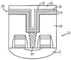
- FIG. 1is a diagrammatic cross-sectional view of a substrate at a preliminary step of a processing sequence.
- FIGS. 2-6are views of the substrate of FIG. 1 at subsequent processing steps according to according to an embodiment of the invention.
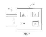
- FIG. 7is a block diagram of a circuit module according to an embodiment of the present invention.
- semiconductor substrateor “semiconductive substrate” or “semiconductive wafer fragment” or “wafer fragment” or “wafer” will be understood to mean any construction comprising semiconductor material, including but not limited to bulk semiconductive materials such as a semiconductor wafer (either alone or in assemblies comprising other materials thereon), and semiconductive material layers (either alone or in assemblies comprising other materials).
- substraterefers to any supporting structure including, but not limited to, the semiconductive substrates, wafer fragments or wafers described above.
- FIGS. 1-6An embodiment of a method according to the invention is described with reference to FIGS. 1-6 , in a method of forming an electrode in a capacitor construction.
- a substrate 10(e.g., a wafer) is shown at a preliminary processing step in the formation of a capacitor.
- the substrate in progresscan comprise, for example, a semiconductor wafer substrate or the wafer along with various process layers formed thereon, including one or more semiconductor layers or other formations, and active or operable portions of semiconductor devices.
- the substrate 10comprises a material layer 12 such as polysilicon, wordlines 14 , and a diffusion region (active area) 16 formed in the material layer 12 between the wordlines, the diffusion region 16 being in the form of a source/drain region.
- a dielectric (insulative) material 18such as borophosphosilicate glass (BPSG), phosphosilicate glass (PSG), or other oxide (e.g., SiOX, TEOS, etc.) or other suitable insulative material has been formed on the material layer 12 and over the wordlines 14 .
- a plug 20 comprising doped polycrystallinehas been deposited into an opening through the insulative layer 18 as an electrical contact with the diffusion region 16 .
- the foregoing structurescan be formed by conventional methods known and used in the art.
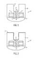
- a container or opening 22 with sidewalls 24 and a base portion or floor 26has been conventionally etched into the insulative layer 18 to expose the plug 20 .
- a lower electrode of rutheniumis then formed within the opening 22 within the insulative material layer 18 .
- an adhesion or nucleation (seed) layer 24is formed on the insulative material layer 18 within the opening to improve adherence of the subsequently deposited ruthenium electrode layer to the insulative material layer 18 .
- An adhesion layer 24 composed of ruthenium silicide (RuSi x )can be formed, for example, by sputter depositing from a deposition target of RuSi x , by physical vapor deposition (PVD) of RuSi x , by atomic layer deposition (ATD), or by chemical vapor deposition (e.g., CVD, LPCVD, APCVD, PECVD, etc.) using a silicon precursor gas and a ruthenium precursor gas.
- PVDphysical vapor deposition
- ATDatomic layer deposition
- CVDchemical vapor deposition
- the adhesion (seed) layer 24can be composed of RuSi x O y and formed, for example, by a process as described, for example, in U.S. Pat. No. 6,461,909 (Marsh et al., Micron Technology, Inc.).
- a RuSi x adhesion layer 24is formed by CVD, for example, by exposing the substrate 10 to a gaseous mixture of a silicon precursor gas and a ruthenium precursor gas at a ratio of about 50:1 to about 1:1 for a duration of about 0.5-20 seconds, or about 1-10 seconds to form the adhesion layer 24 to a thickness of about 1-20 angstroms, or about 1-10 angstroms.
- the flow rate of the silicon precursoris about 1-100 sccm (or about 20-80 sccm)
- the flow rate of the ruthenium precursoris about 1-20 sccm (or about 1-10 sccm)
- the flow rate of an optional carrier gasis about 50-1000 sccm (or about 200-500 sccm).
- General CVD processing parametersinclude a deposition pressure of about 0.1-20 torr, and a deposition temperature at the substrate surface of about 100-700° C., or about 200-500° C..
- the silicon precursoris initially deposited onto the insulative material layer 18 to form a thin seed layer ranging from a monolayer (e.g., about 2 angstroms to about 5 angstroms thick). Both the silicon and ruthenium precursors can then be flowed into the reaction chamber to deposit the RuSi x adhesion layer 24 .
- silicon precursor gasesinclude a silicon hydride or silane such as silane (SiH 4 ), disilane (Si 2 H 6 ), trisilane (Si 3 H 8 ), dichlorosilane (DCS, SiH 2 Cl 2 ), trichlorosilane (TCS, SiHCl 3 ), hexachlorodisilane (Si 2 Cl 6 ), trisilylamine (N(SiH 3 ) 3 ), methylated silanes, among others.
- silaneSiH 4
- disilaneSi 2 H 6
- trisilaneSi 3 H 8
- dichlorosilaneDCS, SiH 2 Cl 2
- trichlorosilaneTCS, SiHCl 3
- hexachlorodisilaneSi 2 Cl 6
- trisilylamineN(SiH 3 ) 3
- methylated silanesamong others.
- ruthenium containing precursorcan be used in accordance with the present disclosure.
- Typical ruthenium precursors for CVD depositioninclude liquid ruthenium metal-organic precursors.
- the ruthenium precursorcan be contained in a bubbler reservoir through which a carrier gas, such as helium or any other inert gas (e.g., nitrogen, argon, neon, and xenon), is bubbled through the reservoir containing the precursor to deliver the precursor to the reaction chamber.
- a carrier gas having a volumetric flow rate in the range of about 1-500 sccmcan be used in a bubbler having a pressure in the range of about 0.5-50 torr and a temperature in the range of about 30-70° C. to deliver a ruthenium precursor to the reaction chamber.
- Ruthenium precursorsinclude liquid ruthenium complexes of the following formula: (diene)Ru(CO) 3 , wherein “diene” refers to linear, branched, or cyclic dienes, bicyclic dienes, tricyclic dienes, fluorinated derivatives thereof, combinations thereof, and derivatives thereof additionally containing heteroatoms such as halide, Si, S, Se, P, As, or N, as described, for example, in U.S. Pat. Nos. 6,063,705 and 5,962,716.
- the ruthenium precursorcan be a ruthenocene having the formula (Cp′)Ru or (Cp′)Ru(Cp′′), where Cp′ and Cp′′ can be the same or different and have the following formula:
- R 1 -R 5can be independently selected from the group consisting of H, F, and straight-chained or branched C 1 -C 5 alkyl groups (e.g., Me, Et, i-Pr, n-Pr, t-Bu, n-Bu, sec-Bu, n-amyl, i-amyl, t-amyl, etc.).
- suitable ruthenocenesinclude bis(cyclopentadienyl)ruthenium, bis(ethylcyclopentadienyl)ruthenium, and bis(pentamethylcyclopentadienyl)ruthenium.
- the ruthenium precursorcan also be a ruthenium ⁇ -diketonate having the formula Ru( ⁇ -diketonate) 3 , wherein the ⁇ -diketonate has the formula:
- R 1 and R 2can be independently selected from the group consisting of H, F, straight-chained or branched C 1 -C 5 alkyl groups (e.g., Me, Et, i-Pr, n-Pr, t-Bu, n-Bu, sec-Bu, n-amyl, t-amyl, etc.), and fluorine-substituted straight-chained or branched C 1 -C 5 alkyl groups (e.g., Me, Et, i-Pr, n-Pr, t-Bu, n-Bu, sec-Bu, n-amyl, i-amyl, t-amyl, etc.).
- C 1 -C 5 alkyl groupse.g., Me, Et, i-Pr, n-Pr, t-Bu, n-Bu, sec-Bu, n-amyl, i-amyl, t-amyl, etc.
- Nonlimiting examples of ⁇ -diketonatesinclude 2,4-pentanedionate; 1,1,1-trifluoro-2,4-pentanedionate; 2,2,6,6-tetramethyl-3,5-heptanedionate; 1,1,1,5,5,5-hexafluoro-2,4-pentanedionate; 2,2,7-tetramethyl-3,5-octanedionato; 6,6,7,7,8,8,8-heptafluoro-2,2-dimethyl-3,5-octanedionato; and 2,4-octanedionato.
- R 1 and R 2are independently selected from the group consisting of C 1 -C 5 fluoroalkyl groups.
- the ruthenium precursorcan also be a ruthenium carbonyl such as Ru(CO) 5 , Ru 3 (CO) 12 , Ru(CO) 9 , (C 6 H 8 )Ru(CO) 3 , and (C 7 H 10 )Ru(CO) 3 , and cyclopentadienyl dicarbonyl ruthenium (II) dimer.
- a ruthenium carbonylsuch as Ru(CO) 5 , Ru 3 (CO) 12 , Ru(CO) 9 , (C 6 H 8 )Ru(CO) 3 , and (C 7 H 10 )Ru(CO) 3 , and cyclopentadienyl dicarbonyl ruthenium (II) dimer.
- a carrier gascan be used to deliver the precursor gas(es) to the reaction chamber, for example, an inert gas such as helium, nitrogen, neon, xenon, and/or argon.
- an inert gassuch as helium, nitrogen, neon, xenon, and/or argon.
- a carrier or dilution gase.g., He, Ar, etc.
- Oxidizing gasescan also be introduced into the reaction chamber when desired.
- a ruthenium layer or film 26is then formed on the adhesion or nucleation (seed) layer 24 by chemical vapor deposition processing (e.g., CVD, LPCVD, APCVD, PECVD, etc.).
- chemical vapor deposition processinge.g., CVD, LPCVD, APCVD, PECVD, etc.
- the flow of the silicon precursoris terminated and a hydrogen source gas is flowed with the ruthenium precursor gas to form a hydrogen-treated ruthenium layer 26 .
- the hydrogen source gasis hydrogen gas (H 2 ), and in other embodiments, ammonia (NH 3 ) is used.
- a carrier gase.g., He, Ar, etc.
- the ruthenium layer 26can by formed by CVD, for example, by exposing the substrate 10 to a gaseous mixture of a ruthenium precursor gas and a hydrogen source gas (e.g., H 2 or NH 3 ) at a ratio of about 0.001:1 to about 1:1 for a duration effective to deposit the desired thickness, generally at least about 100 angstroms, e.g., about 100-300 angstroms, or about 150-250 angstroms.
- a hydrogen source gase.g., H 2 or NH 3
- the flow rate of the ruthenium precursoris about 1-20 sccm (or about 1-10 sccm), and the flow rate of the hydrogen source gas is at least about 200 sccm, and in other embodiments at least about 400 sccm (e.g., about 400-600 sccm).
- the flow rate of an optional carrier gascan be about 50-1000 sccm (or about 200-600 sccm).
- the ruthenium precursor gasflows continuously during CVD processing as the flow of the silicon precursor gas is terminated and flow of the hydrogen source gas is commenced.
- the incorporation of hydrogen in the ruthenium layer 26functions to reduce or eliminate the diffusion of silicon into the bulk ruthenium layer to below detectable levels, particularly in the upper surface of the ruthenium layer 26 (e.g., to a depth of about 10-30 angstroms).
- the incorporation of hydrogencan further function to promote densification and reduce the porosity of the ruthenium layer 26 , increase the stability of the ruthenium layer in air, and improve the uniformity of the ruthenium layer.
- the flow of the hydrogen source gascan be terminated and the ruthenium precursor gas can be flowed to form an additional ruthenium layer 28 over the hydrogen-treated ruthenium layer 26 .
- the ruthenium layer 28can be formed to a desired thickness at about 0-300 angstroms, or about 0-100 angstroms.
- the combined layers 24 , 26 , 28form the lower electrode 30 , which typically has a total thickness of about 50-300 angstroms, or about 50-100 angstroms.
- the surface 32 of the ruthenium electrode 30is substantially or completely silicon-free, i.e., 0-0.01 at.-% silicon by x-ray photoelectron spectroscopy (XPS) and/or secondary ion mass spectroscopy (SIMS) analysis.
- XPSx-ray photoelectron spectroscopy
- SIMSsecondary ion mass spectroscopy
- the resulting ruthenium electrode 30is a graded layer with the content (at.-%) of ruthenium increasing and the silicon concentration decreasing from the adhesion layer (e.g., RuSi x ) 24 to the surface 32 of the ruthenium electrode 30 (e.g., the surface of the hydrogen-treated ruthenium layer 26 ).
- the adhesion layere.g., RuSi x
- the ruthenium electrode 30is a graded layer in which the adhesion layer 24 (e.g., RuSi x ) has a high silicon content of about 10-90 at.-% and ruthenium content of about 10-90 at.-%, with the silicon content decreasing progressively through the hydrogen-treated ruthenium layer 26 to a non-detectable level (ie., 0-0.01 at.-%) at the surface 32 of the ruthenium electrode 30 .
- the ruthenium electrode 30has a surface atomic concentration of ruthenium greater than about 50 at.-%, or about 50-80 at.-% with the resistivity of the film at about 100-1,000% of the bulk ruthenium.
- the resulting electrode 30has a lowered resistivity (Rs value), improved film uniformity, and higher film stability, e.g., in an ambient environment, with little or no degradation occurring upon exposure to air.
- a dielectric (insulating) layer 34is formed on the surface 32 of the ruthenium electrode 30 .
- the dielectric layer 34comprises a dielectric material having a high dielectric constant, for example, greater than about 7, or greater than about 50.
- the dielectric layer 34comprises tantalum oxide Ta 2 O 5 , and/or other metal oxide dielectric material, for example, barium strontium titanate (Ba x Sr (1-x) TiO 3 (BST) where 0 ⁇ x,1), BaTiO 3 , SrTiO 3 , PbTiO 3 , Pb(Zr,Ti)O 3 (PZT), (Pb,La)(Zr,Ti)O 3 (PLZT), (Pb,La)TiO 3 , (PLT), Ta 2 O 5 , KNO 3 , LiNbO 3 , HfO 2 , and/or Al 2 O 3 , among others.
- barium strontium titanateBa x Sr (1-x) TiO 3 (BST) where 0 ⁇ x,1)
- the dielectric layer 34can be formed by conventional methods, for example, RF-magnetron sputtering, chemical vapor deposition (CVD), or other suitable deposition method.
- the dielectric layer 34e.g., Ta 2 O 5
- the dielectric layer 34 formed on the ruthenium electrode 30is properly crystallized with a textured, hexagonal crystalline structure or phase, or will crystallize upon a moderate (about 400-650° C.) thermal anneal.
- the dielectric layercan also be formed from a low k dielectric material, for example, SiO 2 , Si 3 N 4 , or a composite thereof.
- a conductive materialis then deposited to form the upper electrode or plate 36 of the capacitor 38 .
- the top electrode 36can be formed of any conductive material, for example, a metal (e.g., ruthenium, platinum, rhodium, etc.), a conductive metal oxide (e.g., ruthenium oxide, iridium oxide, etc.), or doped polysilicon.
- a metale.g., ruthenium, platinum, rhodium, etc.
- a conductive metal oxidee.g., ruthenium oxide, iridium oxide, etc.
- doped polysilicondoped polysilicon
- FIG. 7is a block diagram of an embodiment of a circuit module 40 in which the present invention can be incorporated.
- modules, devices and systemse.g., processor systems
- incorporating the moduleare described and illustrated in U.S. Pat. No. 6,437,417 (Gilton) and U.S. Pat. No. 6,465,829 (Agarwal), the disclosures of which are incorporated by reference herein.
- two or more dies 42may be combined into a circuit module 40 to enhance or extend the functionality of an individual die 42 .
- Circuit module 40can be a combination of dies 42 representing a variety of functions, or a combination of dies containing the same functionality.
- One or more dies 42 of the circuit modulecan contain circuitry, or integrated circuit devices, that include at least one ruthenium layer 30 or capacitor 30 or other device incorporate the ruthenium layer 30 in accordance with the embodiments of the present invention.
- the integrated circuit devicescan include a memory cell that comprises a ruthenium layer as discussed in the various embodiments in accordance with the invention.
- Circuit module 40can be a subcomponent of a variety of electronic systems, such as a clock, a television, a cell phone, a personal computer, an automobile, an industrial control system, an aircraft, among others. Circuit module 40 will have a variety of leads 44 extending therefrom and coupled to the dies 42 providing unilateral or bilateral communication and control.
- the circuit modulecan be incorporated, for example, into an electronic system that comprises a user interface, for example, a keyboard, monitor, display, printer, speakers, etc.
- a user interfacefor example, a keyboard, monitor, display, printer, speakers, etc.
- One or more circuit modulescan comprise a microprocessor that provides information to the user interface, or is otherwise programmed to carry out particular functions as is known in the art.
- the electronic systemcan comprise, for example, a computer system including a processor and a memory system as a subcomponent, and optionally user interface components, and other associated components such as modems, device driver cards, etc.
- Examples of memory circuitsinclude but are not limited to DRAM (Dynamic Random Access Memory), SRAM (Static Random Access Memory), Flash memories, a synchronous DRAM such as SGRAM (Synchronous Graphics Random Access Memory), SDRAM (Synchronous Dynamic Random Access Memory), SDRAM II, and DDR SDRAM (Double Data Rate SDRAM), as well as Synchlink or Rambus DRAMs and other emerging memory technologies.
- DRAMDynamic Random Access Memory
- SRAMStatic Random Access Memory
- Flash memoriesa synchronous DRAM such as SGRAM (Synchronous Graphics Random Access Memory), SDRAM (Synchronous Dynamic Random Access Memory), SDRAM II, and DDR SDRAM (Double Data Rate SDRAM), as well as Synchlink or Rambus DRAMs and other emerging memory technologies.
Landscapes
- Chemical & Material Sciences (AREA)
- Engineering & Computer Science (AREA)
- Power Engineering (AREA)
- Manufacturing & Machinery (AREA)
- Microelectronics & Electronic Packaging (AREA)
- Inorganic Chemistry (AREA)
- Ceramic Engineering (AREA)
- General Chemical & Material Sciences (AREA)
- Chemical Kinetics & Catalysis (AREA)
- Materials Engineering (AREA)
- Mechanical Engineering (AREA)
- Metallurgy (AREA)
- Organic Chemistry (AREA)
- Electrodes Of Semiconductors (AREA)
- Semiconductor Memories (AREA)
Abstract
Description
- Embodiments of the present disclosure relate to the field of semiconductor manufacture and, more particularly, to methods of forming a ruthenium metal layer in the fabrication of a semiconductor device, and devices resulting from those methods.
- Crystallographically textured tantalum oxide (Ta2O5) demonstrates approximately twice the dielectric permittivity of amorphous Ta2O5, making c-axis textured Ta2O5very attractive as a DRAM cell dielectric. Metallic ruthenium is the bottom cell plate of choice for crystallographically textured, high permittivity Ta2O5cell dielectrics because the Ta2O5orders on the hexagonal close-packed (hcp) ruthenium structure and provides the high permittivity texturing.
- Historically, there have been adhesion issues when ruthenium is deposited on silicon dioxide (SiO2) and other dielectric films. This adhesion issue on oxide dielectrics has been addressed by adding disilane (Si2H6) to the initial stages of ruthenium deposition. However, XPS and SIMS analysis shows that about 20 at.-% silicon is present at the top surface of the deposited ruthenium film, which adversely affects the desired crystographically textured Ta2O5deposition.
- It would be desirable to provide a process for fabricating a ruthenium film that overcomes these problems.
- Embodiments of the invention are described below with reference to the following accompanying drawings, which are for illustrative purposes only.
FIG. 1 is a diagrammatic cross-sectional view of a substrate at a preliminary step of a processing sequence.FIGS. 2-6 are views of the substrate ofFIG. 1 at subsequent processing steps according to according to an embodiment of the invention.FIG. 7 is a block diagram of a circuit module according to an embodiment of the present invention.- The following description provides illustrative examples of devices and methods according to embodiments of the present disclosure. Such description is for illustrative purposes only and not for purposes of limiting the same.
- In the context of the current application, the term “semiconductor substrate” or “semiconductive substrate” or “semiconductive wafer fragment” or “wafer fragment” or “wafer” will be understood to mean any construction comprising semiconductor material, including but not limited to bulk semiconductive materials such as a semiconductor wafer (either alone or in assemblies comprising other materials thereon), and semiconductive material layers (either alone or in assemblies comprising other materials). The term “substrate” refers to any supporting structure including, but not limited to, the semiconductive substrates, wafer fragments or wafers described above.
- An embodiment of a method according to the invention is described with reference to
FIGS. 1-6 , in a method of forming an electrode in a capacitor construction. - Referring to
FIG. 1 , a substrate10 (e.g., a wafer) is shown at a preliminary processing step in the formation of a capacitor. The substrate in progress can comprise, for example, a semiconductor wafer substrate or the wafer along with various process layers formed thereon, including one or more semiconductor layers or other formations, and active or operable portions of semiconductor devices. - In the illustrated embodiment, the
substrate 10 comprises amaterial layer 12 such as polysilicon,wordlines 14, and a diffusion region (active area)16 formed in thematerial layer 12 between the wordlines, thediffusion region 16 being in the form of a source/drain region. A dielectric (insulative)material 18 such as borophosphosilicate glass (BPSG), phosphosilicate glass (PSG), or other oxide (e.g., SiOX, TEOS, etc.) or other suitable insulative material has been formed on thematerial layer 12 and over thewordlines 14. Aplug 20 comprising doped polycrystalline has been deposited into an opening through theinsulative layer 18 as an electrical contact with thediffusion region 16. The foregoing structures can be formed by conventional methods known and used in the art. A container or opening22 withsidewalls 24 and a base portion orfloor 26, has been conventionally etched into theinsulative layer 18 to expose theplug 20. - A lower electrode of ruthenium is then formed within the opening22 within the
insulative material layer 18. - Referring to
FIG. 2 , according to an embodiment of a method of the invention, an adhesion or nucleation (seed)layer 24 is formed on theinsulative material layer 18 within the opening to improve adherence of the subsequently deposited ruthenium electrode layer to theinsulative material layer 18. Anadhesion layer 24 composed of ruthenium silicide (RuSix) can be formed, for example, by sputter depositing from a deposition target of RuSix, by physical vapor deposition (PVD) of RuSix, by atomic layer deposition (ATD), or by chemical vapor deposition (e.g., CVD, LPCVD, APCVD, PECVD, etc.) using a silicon precursor gas and a ruthenium precursor gas. - In other embodiments, the adhesion (seed)
layer 24 can be composed of RuSixOyand formed, for example, by a process as described, for example, in U.S. Pat. No. 6,461,909 (Marsh et al., Micron Technology, Inc.). - In the illustrated embodiment, a RuSixadhesion layer24 is formed by CVD, for example, by exposing the
substrate 10 to a gaseous mixture of a silicon precursor gas and a ruthenium precursor gas at a ratio of about 50:1 to about 1:1 for a duration of about 0.5-20 seconds, or about 1-10 seconds to form theadhesion layer 24 to a thickness of about 1-20 angstroms, or about 1-10 angstroms. In embodiments of the method, the flow rate of the silicon precursor is about 1-100 sccm (or about 20-80 sccm), the flow rate of the ruthenium precursor is about 1-20 sccm (or about 1-10 sccm), and the flow rate of an optional carrier gas is about 50-1000 sccm (or about 200-500 sccm). General CVD processing parameters include a deposition pressure of about 0.1-20 torr, and a deposition temperature at the substrate surface of about 100-700° C., or about 200-500° C.. - In some embodiments, the silicon precursor is initially deposited onto the
insulative material layer 18 to form a thin seed layer ranging from a monolayer (e.g., about 2 angstroms to about 5 angstroms thick). Both the silicon and ruthenium precursors can then be flowed into the reaction chamber to deposit the RuSixadhesion layer24. - Examples of silicon precursor gases include a silicon hydride or silane such as silane (SiH4), disilane (Si2H6), trisilane (Si3H8), dichlorosilane (DCS, SiH2Cl2), trichlorosilane (TCS, SiHCl3), hexachlorodisilane (Si2Cl6), trisilylamine (N(SiH3)3), methylated silanes, among others.
- Any ruthenium containing precursor can be used in accordance with the present disclosure. Typical ruthenium precursors for CVD deposition include liquid ruthenium metal-organic precursors. The ruthenium precursor can be contained in a bubbler reservoir through which a carrier gas, such as helium or any other inert gas (e.g., nitrogen, argon, neon, and xenon), is bubbled through the reservoir containing the precursor to deliver the precursor to the reaction chamber. For example, a carrier gas having a volumetric flow rate in the range of about 1-500 sccm can be used in a bubbler having a pressure in the range of about 0.5-50 torr and a temperature in the range of about 30-70° C. to deliver a ruthenium precursor to the reaction chamber.
- Ruthenium precursors include liquid ruthenium complexes of the following formula: (diene)Ru(CO)3, wherein “diene” refers to linear, branched, or cyclic dienes, bicyclic dienes, tricyclic dienes, fluorinated derivatives thereof, combinations thereof, and derivatives thereof additionally containing heteroatoms such as halide, Si, S, Se, P, As, or N, as described, for example, in U.S. Pat. Nos. 6,063,705 and 5,962,716.
- For example, the ruthenium precursor can be a ruthenocene having the formula (Cp′)Ru or (Cp′)Ru(Cp″), where Cp′ and Cp″ can be the same or different and have the following formula:
- wherein R1-R5can be independently selected from the group consisting of H, F, and straight-chained or branched C1-C5alkyl groups (e.g., Me, Et, i-Pr, n-Pr, t-Bu, n-Bu, sec-Bu, n-amyl, i-amyl, t-amyl, etc.). Nonlimiting examples of suitable ruthenocenes include bis(cyclopentadienyl)ruthenium, bis(ethylcyclopentadienyl)ruthenium, and bis(pentamethylcyclopentadienyl)ruthenium.
- The ruthenium precursor can also be a ruthenium β-diketonate having the formula Ru(β-diketonate)3, wherein the β-diketonate has the formula:
- wherein R1and R2can be independently selected from the group consisting of H, F, straight-chained or branched C1-C5alkyl groups (e.g., Me, Et, i-Pr, n-Pr, t-Bu, n-Bu, sec-Bu, n-amyl, t-amyl, etc.), and fluorine-substituted straight-chained or branched C1-C5alkyl groups (e.g., Me, Et, i-Pr, n-Pr, t-Bu, n-Bu, sec-Bu, n-amyl, i-amyl, t-amyl, etc.). Nonlimiting examples of β-diketonates include 2,4-pentanedionate; 1,1,1-trifluoro-2,4-pentanedionate; 2,2,6,6-tetramethyl-3,5-heptanedionate; 1,1,1,5,5,5-hexafluoro-2,4-pentanedionate; 2,2,7-tetramethyl-3,5-octanedionato; 6,6,7,7,8,8,8-heptafluoro-2,2-dimethyl-3,5-octanedionato; and 2,4-octanedionato. In an embodiment, R1and R2are independently selected from the group consisting of C1-C5fluoroalkyl groups.
- The ruthenium precursor can also be a ruthenium carbonyl such as Ru(CO)5, Ru3(CO)12, Ru(CO)9, (C6H8)Ru(CO)3, and (C7H10)Ru(CO)3, and cyclopentadienyl dicarbonyl ruthenium (II) dimer.
- Additional precursors and methods of depositing ruthenium layers are generally discussed in U.S. Pat. No. 5,372,849 to McCormick et al. (Minnesota Mining and Manufacturing Company (St. Paul, Minn.)).
- A carrier gas can be used to deliver the precursor gas(es) to the reaction chamber, for example, an inert gas such as helium, nitrogen, neon, xenon, and/or argon. Optionally, a carrier or dilution gas (e.g., He, Ar, etc.) can be introduced into the reaction chamber to alter the concentrations of the gases therein, for example, at a varied flow rate. Oxidizing gases can also be introduced into the reaction chamber when desired.
- Referring now to
FIG. 3 , a ruthenium layer orfilm 26 is then formed on the adhesion or nucleation (seed)layer 24 by chemical vapor deposition processing (e.g., CVD, LPCVD, APCVD, PECVD, etc.). The flow of the silicon precursor is terminated and a hydrogen source gas is flowed with the ruthenium precursor gas to form a hydrogen-treatedruthenium layer 26. In embodiments of the method, the hydrogen source gas is hydrogen gas (H2), and in other embodiments, ammonia (NH3) is used. Optionally, a carrier gas (e.g., He, Ar, etc.) can be used. CVD processing conditions can be as described for forming the RuSixadhesion layer24. Theruthenium layer 26 can by formed by CVD, for example, by exposing thesubstrate 10 to a gaseous mixture of a ruthenium precursor gas and a hydrogen source gas (e.g., H2or NH3) at a ratio of about 0.001:1 to about 1:1 for a duration effective to deposit the desired thickness, generally at least about 100 angstroms, e.g., about 100-300 angstroms, or about 150-250 angstroms. In embodiments of the method, the flow rate of the ruthenium precursor is about 1-20 sccm (or about 1-10 sccm), and the flow rate of the hydrogen source gas is at least about 200 sccm, and in other embodiments at least about 400 sccm (e.g., about 400-600 sccm). The flow rate of an optional carrier gas can be about 50-1000 sccm (or about 200-600 sccm). In an embodiment, the ruthenium precursor gas flows continuously during CVD processing as the flow of the silicon precursor gas is terminated and flow of the hydrogen source gas is commenced. - The incorporation of hydrogen in the
ruthenium layer 26 functions to reduce or eliminate the diffusion of silicon into the bulk ruthenium layer to below detectable levels, particularly in the upper surface of the ruthenium layer26 (e.g., to a depth of about 10-30 angstroms). The incorporation of hydrogen can further function to promote densification and reduce the porosity of theruthenium layer 26, increase the stability of the ruthenium layer in air, and improve the uniformity of the ruthenium layer. - Optionally, as depicted in
FIG. 4 , in some embodiments, the flow of the hydrogen source gas can be terminated and the ruthenium precursor gas can be flowed to form anadditional ruthenium layer 28 over the hydrogen-treatedruthenium layer 26. Theruthenium layer 28 can be formed to a desired thickness at about 0-300 angstroms, or about 0-100 angstroms. The combined layers24,26,28 form thelower electrode 30, which typically has a total thickness of about 50-300 angstroms, or about 50-100 angstroms. - Due, at least in part, to the addition of the hydrogen source gas during the formation of the
ruthenium material layer 26, diffusion of silicon from the initial adhesion (seed)layer 24 into the upper portion of the hydrogen-treatedruthenium layer 26 is eliminated and thesurface 32 of theruthenium electrode 30 is substantially or completely silicon-free, i.e., 0-0.01 at.-% silicon by x-ray photoelectron spectroscopy (XPS) and/or secondary ion mass spectroscopy (SIMS) analysis. The resultingruthenium electrode 30 is a graded layer with the content (at.-%) of ruthenium increasing and the silicon concentration decreasing from the adhesion layer (e.g., RuSix)24 to thesurface 32 of the ruthenium electrode30 (e.g., the surface of the hydrogen-treated ruthenium layer26). In some embodiments, theruthenium electrode 30 is a graded layer in which the adhesion layer24 (e.g., RuSix) has a high silicon content of about 10-90 at.-% and ruthenium content of about 10-90 at.-%, with the silicon content decreasing progressively through the hydrogen-treatedruthenium layer 26 to a non-detectable level (ie., 0-0.01 at.-%) at thesurface 32 of theruthenium electrode 30. In some embodiments, theruthenium electrode 30 has a surface atomic concentration of ruthenium greater than about 50 at.-%, or about 50-80 at.-% with the resistivity of the film at about 100-1,000% of the bulk ruthenium. - The resulting
electrode 30 has a lowered resistivity (Rs value), improved film uniformity, and higher film stability, e.g., in an ambient environment, with little or no degradation occurring upon exposure to air. - Referring now to
FIG. 5 , a dielectric (insulating)layer 34 is formed on thesurface 32 of theruthenium electrode 30. In embodiments of the invention, thedielectric layer 34 comprises a dielectric material having a high dielectric constant, for example, greater than about 7, or greater than about 50. In some embodiments, thedielectric layer 34 comprises tantalum oxide Ta2O5, and/or other metal oxide dielectric material, for example, barium strontium titanate (BaxSr(1-x)TiO3(BST) where 0<x,1), BaTiO3, SrTiO3, PbTiO3, Pb(Zr,Ti)O3(PZT), (Pb,La)(Zr,Ti)O3(PLZT), (Pb,La)TiO3, (PLT), Ta2O5, KNO3, LiNbO3, HfO2, and/or Al2O3, among others. Thedielectric layer 34 can be formed by conventional methods, for example, RF-magnetron sputtering, chemical vapor deposition (CVD), or other suitable deposition method. The dielectric layer34 (e.g., Ta2O5) formed on theruthenium electrode 30 is properly crystallized with a textured, hexagonal crystalline structure or phase, or will crystallize upon a moderate (about 400-650° C.) thermal anneal. - The dielectric layer can also be formed from a low k dielectric material, for example, SiO2, Si3N4, or a composite thereof.
- As illustrated in
FIG. 6 , a conductive material is then deposited to form the upper electrode orplate 36 of thecapacitor 38. Thetop electrode 36 can be formed of any conductive material, for example, a metal (e.g., ruthenium, platinum, rhodium, etc.), a conductive metal oxide (e.g., ruthenium oxide, iridium oxide, etc.), or doped polysilicon. The layers can then be patterned by known techniques as conventional in the art, and the substrate further processed as desired. FIG. 7 is a block diagram of an embodiment of acircuit module 40 in which the present invention can be incorporated. Such modules, devices and systems (e.g., processor systems) incorporating the module are described and illustrated in U.S. Pat. No. 6,437,417 (Gilton) and U.S. Pat. No. 6,465,829 (Agarwal), the disclosures of which are incorporated by reference herein. In brief, two or more dies42 may be combined into acircuit module 40 to enhance or extend the functionality of anindividual die 42.Circuit module 40 can be a combination of dies42 representing a variety of functions, or a combination of dies containing the same functionality. One or more dies42 of the circuit module can contain circuitry, or integrated circuit devices, that include at least oneruthenium layer 30 orcapacitor 30 or other device incorporate theruthenium layer 30 in accordance with the embodiments of the present invention. The integrated circuit devices can include a memory cell that comprises a ruthenium layer as discussed in the various embodiments in accordance with the invention.- Some examples of a circuit module include memory modules, device drivers, power modules, communication modems, processor modules, and application-specific modules, and may include multilayer, multichip modules.
Circuit module 40 can be a subcomponent of a variety of electronic systems, such as a clock, a television, a cell phone, a personal computer, an automobile, an industrial control system, an aircraft, among others.Circuit module 40 will have a variety ofleads 44 extending therefrom and coupled to the dies42 providing unilateral or bilateral communication and control. - The circuit module can be incorporated, for example, into an electronic system that comprises a user interface, for example, a keyboard, monitor, display, printer, speakers, etc. One or more circuit modules can comprise a microprocessor that provides information to the user interface, or is otherwise programmed to carry out particular functions as is known in the art. The electronic system can comprise, for example, a computer system including a processor and a memory system as a subcomponent, and optionally user interface components, and other associated components such as modems, device driver cards, etc. Examples of memory circuits include but are not limited to DRAM (Dynamic Random Access Memory), SRAM (Static Random Access Memory), Flash memories, a synchronous DRAM such as SGRAM (Synchronous Graphics Random Access Memory), SDRAM (Synchronous Dynamic Random Access Memory), SDRAM II, and DDR SDRAM (Double Data Rate SDRAM), as well as Synchlink or Rambus DRAMs and other emerging memory technologies.
- Although specific embodiments have been illustrated and described herein, it will be appreciated by those of ordinary skill in the art that any arrangement which is calculated to achieve the same purpose can be substituted for the specific embodiments shown. This application is intended to cover any adaptations or variations that operate according to the principles of this disclosure as described herein. It is therefore intended that such changes and modifications be covered by the appended claims and the equivalents thereof. The disclosures of patents, references and publications cited in the application are incorporated by reference herein.


Claims (45)
Priority Applications (3)
| Application Number | Priority Date | Filing Date | Title |
|---|---|---|---|
| US12/100,632US8124528B2 (en) | 2008-04-10 | 2008-04-10 | Method for forming a ruthenium film |
| US13/407,185US8513807B2 (en) | 2008-04-10 | 2012-02-28 | Semiconductor devices including a ruthenium film |
| US13/950,583US8900992B2 (en) | 2008-04-10 | 2013-07-25 | Methods of forming a ruthenium material, methods of forming a capacitor, and related electronic systems |
Applications Claiming Priority (1)
| Application Number | Priority Date | Filing Date | Title |
|---|---|---|---|
| US12/100,632US8124528B2 (en) | 2008-04-10 | 2008-04-10 | Method for forming a ruthenium film |
Related Child Applications (1)
| Application Number | Title | Priority Date | Filing Date |
|---|---|---|---|
| US13/407,185DivisionUS8513807B2 (en) | 2008-04-10 | 2012-02-28 | Semiconductor devices including a ruthenium film |
Publications (2)
| Publication Number | Publication Date |
|---|---|
| US20090257170A1true US20090257170A1 (en) | 2009-10-15 |
| US8124528B2 US8124528B2 (en) | 2012-02-28 |
Family
ID=41163794
Family Applications (3)
| Application Number | Title | Priority Date | Filing Date |
|---|---|---|---|
| US12/100,632Active2028-04-15US8124528B2 (en) | 2008-04-10 | 2008-04-10 | Method for forming a ruthenium film |
| US13/407,185ActiveUS8513807B2 (en) | 2008-04-10 | 2012-02-28 | Semiconductor devices including a ruthenium film |
| US13/950,583Active2028-04-23US8900992B2 (en) | 2008-04-10 | 2013-07-25 | Methods of forming a ruthenium material, methods of forming a capacitor, and related electronic systems |
Family Applications After (2)
| Application Number | Title | Priority Date | Filing Date |
|---|---|---|---|
| US13/407,185ActiveUS8513807B2 (en) | 2008-04-10 | 2012-02-28 | Semiconductor devices including a ruthenium film |
| US13/950,583Active2028-04-23US8900992B2 (en) | 2008-04-10 | 2013-07-25 | Methods of forming a ruthenium material, methods of forming a capacitor, and related electronic systems |
Country Status (1)
| Country | Link |
|---|---|
| US (3) | US8124528B2 (en) |
Cited By (7)
| Publication number | Priority date | Publication date | Assignee | Title |
|---|---|---|---|---|
| US20130260529A1 (en)* | 2011-02-07 | 2013-10-03 | Micron Technology, Inc. | Methods of forming capacitors and semiconductor devices including a rutile titanium dioxide material |
| US8609553B2 (en) | 2011-02-07 | 2013-12-17 | Micron Technology, Inc. | Methods of forming rutile titanium dioxide and associated methods of forming semiconductor structures |
| US8900992B2 (en) | 2008-04-10 | 2014-12-02 | Micron Technology, Inc. | Methods of forming a ruthenium material, methods of forming a capacitor, and related electronic systems |
| US8940388B2 (en) | 2011-03-02 | 2015-01-27 | Micron Technology, Inc. | Insulative elements |
| US20200208260A1 (en)* | 2018-12-27 | 2020-07-02 | Tokyo Electron Limited | Method of Forming RuSi Film and Film and Film-Forming Apparatus |
| KR20210009278A (en)* | 2019-07-16 | 2021-01-26 | 도쿄엘렉트론가부시키가이샤 | METHOD FOR FORMING RuSi FILM AND SUBSTRATE PROCESSING SYSTEM |
| US11371138B2 (en)* | 2018-11-08 | 2022-06-28 | Entegris, Inc. | Chemical vapor deposition processes using ruthenium precursor and reducing gas |
Families Citing this family (2)
| Publication number | Priority date | Publication date | Assignee | Title |
|---|---|---|---|---|
| US20210252486A1 (en)* | 2018-06-22 | 2021-08-19 | The Curators Of The University Of Missouri | Novel method of manufacture of metal nanoparticles and metal single-atom materials on various substrates and novel compositions |
| KR20220009249A (en) | 2020-07-15 | 2022-01-24 | 엘지디스플레이 주식회사 | Display device and method of manufacturing the same |
Citations (37)
| Publication number | Priority date | Publication date | Assignee | Title |
|---|---|---|---|---|
| US5372849A (en)* | 1992-07-28 | 1994-12-13 | Minnesota Mining And Manufacturing Company | Chemical vapor deposition of iron, ruthenium, and osmium |
| US5962716A (en)* | 1998-08-27 | 1999-10-05 | Micron Technology, Inc. | Methods for preparing ruthenium and osmium compounds |
| US6063705A (en)* | 1998-08-27 | 2000-05-16 | Micron Technology, Inc. | Precursor chemistries for chemical vapor deposition of ruthenium and ruthenium oxide |
| US6197628B1 (en)* | 1998-08-27 | 2001-03-06 | Micron Technology, Inc. | Ruthenium silicide diffusion barrier layers and methods of forming same |
| US6281125B1 (en)* | 1998-08-27 | 2001-08-28 | Micron Technology, Inc. | Methods for preparing ruthenium oxide films |
| US20010020715A1 (en)* | 2000-03-02 | 2001-09-13 | Tokyo Electron Limited | Semiconductor device and manufacturing method therefor |
| US20020013052A1 (en)* | 2000-03-08 | 2002-01-31 | Visokay Mark R. | Methods for preparing ruthenium metal films |
| US6437417B1 (en)* | 2000-08-16 | 2002-08-20 | Micron Technology, Inc. | Method for making shallow trenches for isolation |
| US20020142538A1 (en)* | 2000-08-30 | 2002-10-03 | Marsh Eugene P. | Process for fabricating RuSixOy-containing adhesion layers |
| US6465828B2 (en)* | 1999-07-30 | 2002-10-15 | Micron Technology, Inc. | Semiconductor container structure with diffusion barrier |
| US20030015769A1 (en)* | 1998-02-26 | 2003-01-23 | Micron Technology, Inc. | Capacitor having tantalum oxynitride film and method for making same |
| US20030109110A1 (en)* | 2001-12-10 | 2003-06-12 | Kim Kyong Min | Method for forming capacitor of a semiconductor device |
| US20030213986A1 (en)* | 2001-04-25 | 2003-11-20 | Fujitsu Limited | Semiconductor device having a ferroelectric capacitor and fabrication process thereof |
| US6734100B2 (en)* | 2001-12-20 | 2004-05-11 | Jusung Engineering Co., Ltd. | Method of forming ruthenium thin film using plasma enhanced process |
| US6737313B1 (en)* | 2003-04-16 | 2004-05-18 | Micron Technology, Inc. | Surface treatment of an oxide layer to enhance adhesion of a ruthenium metal layer |
| US6824816B2 (en)* | 2002-01-29 | 2004-11-30 | Asm International N.V. | Process for producing metal thin films by ALD |
| US20050221002A1 (en)* | 2004-03-31 | 2005-10-06 | Tokyo Electron Limited | Method for processing a substrate |
| US20050238808A1 (en)* | 2004-04-27 | 2005-10-27 | L'Air Liquide, Société Anonyme à Directoire et Conseil de Surveillance pour I'Etude et I'Exploita | Methods for producing ruthenium film and ruthenium oxide film |
| US7002033B1 (en)* | 2004-07-27 | 2006-02-21 | Jsr Corporation | Chemical vapor deposition material and chemical vapor deposition |
| US20060145294A1 (en)* | 2003-08-06 | 2006-07-06 | Vishwanath Bhat | Methods of forming capacitors |
| US20060177601A1 (en)* | 2005-02-10 | 2006-08-10 | Hyung-Sang Park | Method of forming a ruthenium thin film using a plasma enhanced atomic layer deposition apparatus and the method thereof |
| US20060251813A1 (en)* | 2004-04-08 | 2006-11-09 | Carlson Chris M | Methods of forming material over substrates |
| US7148555B2 (en)* | 2002-01-16 | 2006-12-12 | Micron Technology, Inc. | Method for enhancing electrode surface area in DRAM cell capacitors |
| US20070037392A1 (en)* | 2005-08-08 | 2007-02-15 | Thompson Jeffery S | Atomic layer deposition of ruthenium-containing films using surface-activating agents and novel ruthenium complexes |
| US20070082132A1 (en)* | 2005-10-07 | 2007-04-12 | Asm Japan K.K. | Method for forming metal wiring structure |
| US20070111434A1 (en)* | 2005-11-14 | 2007-05-17 | Elpida Memory, Inc. | Method for manufacturing capacitor |
| US20070148896A1 (en)* | 2003-02-14 | 2007-06-28 | Elpida Memory, Inc | Memory with memory cells that include a mim type capacitor with a lower electrode made for reduced resistance at an interface with a metal film |
| US20070160756A1 (en)* | 2006-01-07 | 2007-07-12 | Helmuth Treichel | Apparatus and method for the deposition of ruthenium containing films |
| US20070190782A1 (en)* | 2006-02-15 | 2007-08-16 | Hyung-Sang Park | Method of depositing Ru films having high density |
| US20070190781A1 (en)* | 2002-03-29 | 2007-08-16 | Micron Technology, Inc. | Methods of forming metal-containing films over surfaces of semiconductor substrates |
| US20070207588A1 (en)* | 2000-06-21 | 2007-09-06 | Micron Technology, Inc. | Structures and methods for enhancing capacitors in integrated circuits |
| US20070218316A1 (en)* | 2006-03-20 | 2007-09-20 | Fujitsu Limited | Magnetic recording medium, method of producing same, and magnetic storage apparatus |
| US20070218205A1 (en)* | 2004-02-23 | 2007-09-20 | Advanced Technology Materials, Inc. | Chemical vapor deposition of high conductivity, adherent thin films of ruthenium |
| US20070231927A1 (en)* | 2006-04-03 | 2007-10-04 | Koji Yamakawa | Semiconductor device and manufacturing method thereof |
| US20070264838A1 (en)* | 2006-05-10 | 2007-11-15 | Micron Technology, Inc. | Electrical components for microelectronic devices and methods of forming the same |
| US20090022891A1 (en)* | 2006-02-08 | 2009-01-22 | Jsr Corporation | Method of forming metal film |
| US20090035466A1 (en)* | 2006-02-28 | 2009-02-05 | Tokyo Electron Limited | Ruthenium film formation method and computer readable storage medium |
Family Cites Families (10)
| Publication number | Priority date | Publication date | Assignee | Title |
|---|---|---|---|---|
| JP3905977B2 (en) | 1998-05-22 | 2007-04-18 | 株式会社東芝 | Manufacturing method of semiconductor device |
| JP4261021B2 (en) | 1999-05-14 | 2009-04-30 | パナソニック株式会社 | Semiconductor device and manufacturing method thereof |
| JP3624822B2 (en)* | 2000-11-22 | 2005-03-02 | 株式会社日立製作所 | Semiconductor device and manufacturing method thereof |
| KR100522762B1 (en) | 2001-12-19 | 2005-10-24 | 주식회사 하이닉스반도체 | Method for Chemical Vapor Deposition of metal film |
| US7098128B2 (en)* | 2004-09-01 | 2006-08-29 | Micron Technology, Inc. | Method for filling electrically different features |
| US7273814B2 (en)* | 2005-03-16 | 2007-09-25 | Tokyo Electron Limited | Method for forming a ruthenium metal layer on a patterned substrate |
| JP2006324363A (en)* | 2005-05-17 | 2006-11-30 | Elpida Memory Inc | Capacitor and manufacturing method thereof |
| JP5339397B2 (en) | 2005-08-29 | 2013-11-13 | 芝浦メカトロニクス株式会社 | Manufacturing method of electronic device |
| US8068315B2 (en)* | 2007-09-26 | 2011-11-29 | Hitachi Global Storage Technologies Netherlands B.V. | Current perpendicular to plane GMR and TMR sensors with improved magnetic properties using Ru/Si seed layers |
| US8124528B2 (en) | 2008-04-10 | 2012-02-28 | Micron Technology, Inc. | Method for forming a ruthenium film |
- 2008
- 2008-04-10USUS12/100,632patent/US8124528B2/enactiveActive
- 2012
- 2012-02-28USUS13/407,185patent/US8513807B2/enactiveActive
- 2013
- 2013-07-25USUS13/950,583patent/US8900992B2/enactiveActive
Patent Citations (43)
| Publication number | Priority date | Publication date | Assignee | Title |
|---|---|---|---|---|
| US5372849A (en)* | 1992-07-28 | 1994-12-13 | Minnesota Mining And Manufacturing Company | Chemical vapor deposition of iron, ruthenium, and osmium |
| US20030015769A1 (en)* | 1998-02-26 | 2003-01-23 | Micron Technology, Inc. | Capacitor having tantalum oxynitride film and method for making same |
| US20050161710A1 (en)* | 1998-02-26 | 2005-07-28 | Micron Technology, Inc. | Capacitor having tantalum oxynitride film and method for making same |
| US5962716A (en)* | 1998-08-27 | 1999-10-05 | Micron Technology, Inc. | Methods for preparing ruthenium and osmium compounds |
| US6063705A (en)* | 1998-08-27 | 2000-05-16 | Micron Technology, Inc. | Precursor chemistries for chemical vapor deposition of ruthenium and ruthenium oxide |
| US6197628B1 (en)* | 1998-08-27 | 2001-03-06 | Micron Technology, Inc. | Ruthenium silicide diffusion barrier layers and methods of forming same |
| US6281125B1 (en)* | 1998-08-27 | 2001-08-28 | Micron Technology, Inc. | Methods for preparing ruthenium oxide films |
| US6465828B2 (en)* | 1999-07-30 | 2002-10-15 | Micron Technology, Inc. | Semiconductor container structure with diffusion barrier |
| US6846711B2 (en)* | 2000-03-02 | 2005-01-25 | Tokyo Electron Limited | Method of making a metal oxide capacitor, including a barrier film |
| US20010020715A1 (en)* | 2000-03-02 | 2001-09-13 | Tokyo Electron Limited | Semiconductor device and manufacturing method therefor |
| US20020013052A1 (en)* | 2000-03-08 | 2002-01-31 | Visokay Mark R. | Methods for preparing ruthenium metal films |
| US20070207588A1 (en)* | 2000-06-21 | 2007-09-06 | Micron Technology, Inc. | Structures and methods for enhancing capacitors in integrated circuits |
| US6437417B1 (en)* | 2000-08-16 | 2002-08-20 | Micron Technology, Inc. | Method for making shallow trenches for isolation |
| US6461909B1 (en)* | 2000-08-30 | 2002-10-08 | Micron Technology, Inc. | Process for fabricating RuSixOy-containing adhesion layers |
| US6764895B2 (en)* | 2000-08-30 | 2004-07-20 | Micron Technology, Inc. | Process for fabricating RuSixOy-containing adhesion layers |
| US6462367B2 (en)* | 2000-08-30 | 2002-10-08 | Micron Technology, Inc. | RuSixOy-containing adhesion layers |
| US20020142538A1 (en)* | 2000-08-30 | 2002-10-03 | Marsh Eugene P. | Process for fabricating RuSixOy-containing adhesion layers |
| US20030213986A1 (en)* | 2001-04-25 | 2003-11-20 | Fujitsu Limited | Semiconductor device having a ferroelectric capacitor and fabrication process thereof |
| US20030109110A1 (en)* | 2001-12-10 | 2003-06-12 | Kim Kyong Min | Method for forming capacitor of a semiconductor device |
| US6734100B2 (en)* | 2001-12-20 | 2004-05-11 | Jusung Engineering Co., Ltd. | Method of forming ruthenium thin film using plasma enhanced process |
| US7148555B2 (en)* | 2002-01-16 | 2006-12-12 | Micron Technology, Inc. | Method for enhancing electrode surface area in DRAM cell capacitors |
| US20050020060A1 (en)* | 2002-01-29 | 2005-01-27 | Titta Aaltonen | Process for producing metal thin films by ALD |
| US6824816B2 (en)* | 2002-01-29 | 2004-11-30 | Asm International N.V. | Process for producing metal thin films by ALD |
| US20070190781A1 (en)* | 2002-03-29 | 2007-08-16 | Micron Technology, Inc. | Methods of forming metal-containing films over surfaces of semiconductor substrates |
| US20070148896A1 (en)* | 2003-02-14 | 2007-06-28 | Elpida Memory, Inc | Memory with memory cells that include a mim type capacitor with a lower electrode made for reduced resistance at an interface with a metal film |
| US6737313B1 (en)* | 2003-04-16 | 2004-05-18 | Micron Technology, Inc. | Surface treatment of an oxide layer to enhance adhesion of a ruthenium metal layer |
| US20060145294A1 (en)* | 2003-08-06 | 2006-07-06 | Vishwanath Bhat | Methods of forming capacitors |
| US20070218205A1 (en)* | 2004-02-23 | 2007-09-20 | Advanced Technology Materials, Inc. | Chemical vapor deposition of high conductivity, adherent thin films of ruthenium |
| US20050221002A1 (en)* | 2004-03-31 | 2005-10-06 | Tokyo Electron Limited | Method for processing a substrate |
| US20060251813A1 (en)* | 2004-04-08 | 2006-11-09 | Carlson Chris M | Methods of forming material over substrates |
| US20050238808A1 (en)* | 2004-04-27 | 2005-10-27 | L'Air Liquide, Société Anonyme à Directoire et Conseil de Surveillance pour I'Etude et I'Exploita | Methods for producing ruthenium film and ruthenium oxide film |
| US7002033B1 (en)* | 2004-07-27 | 2006-02-21 | Jsr Corporation | Chemical vapor deposition material and chemical vapor deposition |
| US20060177601A1 (en)* | 2005-02-10 | 2006-08-10 | Hyung-Sang Park | Method of forming a ruthenium thin film using a plasma enhanced atomic layer deposition apparatus and the method thereof |
| US20070037392A1 (en)* | 2005-08-08 | 2007-02-15 | Thompson Jeffery S | Atomic layer deposition of ruthenium-containing films using surface-activating agents and novel ruthenium complexes |
| US20070082132A1 (en)* | 2005-10-07 | 2007-04-12 | Asm Japan K.K. | Method for forming metal wiring structure |
| US20070111434A1 (en)* | 2005-11-14 | 2007-05-17 | Elpida Memory, Inc. | Method for manufacturing capacitor |
| US20070160756A1 (en)* | 2006-01-07 | 2007-07-12 | Helmuth Treichel | Apparatus and method for the deposition of ruthenium containing films |
| US20090022891A1 (en)* | 2006-02-08 | 2009-01-22 | Jsr Corporation | Method of forming metal film |
| US20070190782A1 (en)* | 2006-02-15 | 2007-08-16 | Hyung-Sang Park | Method of depositing Ru films having high density |
| US20090035466A1 (en)* | 2006-02-28 | 2009-02-05 | Tokyo Electron Limited | Ruthenium film formation method and computer readable storage medium |
| US20070218316A1 (en)* | 2006-03-20 | 2007-09-20 | Fujitsu Limited | Magnetic recording medium, method of producing same, and magnetic storage apparatus |
| US20070231927A1 (en)* | 2006-04-03 | 2007-10-04 | Koji Yamakawa | Semiconductor device and manufacturing method thereof |
| US20070264838A1 (en)* | 2006-05-10 | 2007-11-15 | Micron Technology, Inc. | Electrical components for microelectronic devices and methods of forming the same |
Cited By (20)
| Publication number | Priority date | Publication date | Assignee | Title |
|---|---|---|---|---|
| US8900992B2 (en) | 2008-04-10 | 2014-12-02 | Micron Technology, Inc. | Methods of forming a ruthenium material, methods of forming a capacitor, and related electronic systems |
| US9159731B2 (en)* | 2011-02-07 | 2015-10-13 | Micron Technology, Inc. | Methods of forming capacitors and semiconductor devices including a rutile titanium dioxide material |
| US8748283B2 (en)* | 2011-02-07 | 2014-06-10 | Micron Technology, Inc. | Methods of forming capacitors and semiconductor devices including a rutile titanium dioxide material |
| US20130260529A1 (en)* | 2011-02-07 | 2013-10-03 | Micron Technology, Inc. | Methods of forming capacitors and semiconductor devices including a rutile titanium dioxide material |
| US8564095B2 (en) | 2011-02-07 | 2013-10-22 | Micron Technology, Inc. | Capacitors including a rutile titanium dioxide material and semiconductor devices incorporating same |
| US8927441B2 (en) | 2011-02-07 | 2015-01-06 | Micron Technology, Inc. | Methods of forming rutile titanium dioxide |
| US8936991B2 (en)* | 2011-02-07 | 2015-01-20 | Micron Technology, Inc. | Methods of forming capacitors and semiconductor devices including a rutile titanium dioxide material |
| US8609553B2 (en) | 2011-02-07 | 2013-12-17 | Micron Technology, Inc. | Methods of forming rutile titanium dioxide and associated methods of forming semiconductor structures |
| US20150093874A1 (en)* | 2011-02-07 | 2015-04-02 | Micron Technology, Inc. | Methods of forming capacitors and semiconductor devices including a rutile titanium dioxide material |
| US20140210049A1 (en)* | 2011-02-07 | 2014-07-31 | Micron Technology, Inc. | Methods of forming capacitors and semiconductor devices including a rutile titanium dioxide material |
| US8940388B2 (en) | 2011-03-02 | 2015-01-27 | Micron Technology, Inc. | Insulative elements |
| US11371138B2 (en)* | 2018-11-08 | 2022-06-28 | Entegris, Inc. | Chemical vapor deposition processes using ruthenium precursor and reducing gas |
| US11987878B2 (en) | 2018-11-08 | 2024-05-21 | Entegris, Inc. | Chemical vapor deposition processes using ruthenium precursor and reducing gas |
| US20200208260A1 (en)* | 2018-12-27 | 2020-07-02 | Tokyo Electron Limited | Method of Forming RuSi Film and Film and Film-Forming Apparatus |
| KR102394115B1 (en) | 2019-07-16 | 2022-05-04 | 도쿄엘렉트론가부시키가이샤 | METHOD FOR FORMING RuSi FILM AND SUBSTRATE PROCESSING SYSTEM |
| JP2021015947A (en)* | 2019-07-16 | 2021-02-12 | 東京エレクトロン株式会社 | FORMING METHOD OF RuSi FILM AND SUBSTRATE PROCESSING SYSTEM |
| JP7296806B2 (en) | 2019-07-16 | 2023-06-23 | 東京エレクトロン株式会社 | RuSi film forming method and substrate processing system |
| US11981992B2 (en)* | 2019-07-16 | 2024-05-14 | Tokyo Electron Limited | Method for forming RuSi film and substrate processing system |
| KR20210009278A (en)* | 2019-07-16 | 2021-01-26 | 도쿄엘렉트론가부시키가이샤 | METHOD FOR FORMING RuSi FILM AND SUBSTRATE PROCESSING SYSTEM |
| TWI848144B (en)* | 2019-07-16 | 2024-07-11 | 日商東京威力科創股份有限公司 | RuSi film forming method and substrate processing system |
Also Published As
| Publication number | Publication date |
|---|---|
| US20130307120A1 (en) | 2013-11-21 |
| US8900992B2 (en) | 2014-12-02 |
| US20120161282A1 (en) | 2012-06-28 |
| US8513807B2 (en) | 2013-08-20 |
| US8124528B2 (en) | 2012-02-28 |
Similar Documents
| Publication | Publication Date | Title |
|---|---|---|
| US8900992B2 (en) | Methods of forming a ruthenium material, methods of forming a capacitor, and related electronic systems | |
| US6462367B2 (en) | RuSixOy-containing adhesion layers | |
| US6743739B2 (en) | Fabrication method for semiconductor integrated devices | |
| US6319832B1 (en) | Methods of making semiconductor devices | |
| JP4719358B2 (en) | Capacitor manufacturing method | |
| US20020190276A1 (en) | Process for the formation of RuSixOy-containing barrier layers for high-k dielectrics | |
| US20020102826A1 (en) | Fabricating method of semiconductor integrated circuits | |
| US7071053B2 (en) | Method of forming capacitor with ruthenium top and bottom electrodes by MOCVD | |
| US7271053B2 (en) | Methods of forming capacitors and electronic devices | |
| US6734100B2 (en) | Method of forming ruthenium thin film using plasma enhanced process | |
| JP2002033462A (en) | Method for manufacturing semiconductor device | |
| Kim et al. | Microstructural Characterization of MOCVD RuOx Thin Films and Effects of Annealing Gas Ambient | |
| KR20040001489A (en) | method for fabricating capacitor |
Legal Events
| Date | Code | Title | Description |
|---|---|---|---|
| AS | Assignment | Owner name:MICRON TECHNOLOGY, INC., IDAHO Free format text:ASSIGNMENT OF ASSIGNORS INTEREST;ASSIGNORS:BHAT, VISHWANATH;GEALY, DAN;ANTONOV, VASSIL;REEL/FRAME:020784/0366;SIGNING DATES FROM 20080314 TO 20080408 Owner name:MICRON TECHNOLOGY, INC., IDAHO Free format text:ASSIGNMENT OF ASSIGNORS INTEREST;ASSIGNORS:BHAT, VISHWANATH;GEALY, DAN;ANTONOV, VASSIL;SIGNING DATES FROM 20080314 TO 20080408;REEL/FRAME:020784/0366 | |
| FEPP | Fee payment procedure | Free format text:PAYOR NUMBER ASSIGNED (ORIGINAL EVENT CODE: ASPN); ENTITY STATUS OF PATENT OWNER: LARGE ENTITY | |
| STCF | Information on status: patent grant | Free format text:PATENTED CASE | |
| FPAY | Fee payment | Year of fee payment:4 | |
| AS | Assignment | Owner name:U.S. BANK NATIONAL ASSOCIATION, AS COLLATERAL AGENT, CALIFORNIA Free format text:SECURITY INTEREST;ASSIGNOR:MICRON TECHNOLOGY, INC.;REEL/FRAME:038669/0001 Effective date:20160426 Owner name:U.S. BANK NATIONAL ASSOCIATION, AS COLLATERAL AGEN Free format text:SECURITY INTEREST;ASSIGNOR:MICRON TECHNOLOGY, INC.;REEL/FRAME:038669/0001 Effective date:20160426 | |
| AS | Assignment | Owner name:MORGAN STANLEY SENIOR FUNDING, INC., AS COLLATERAL AGENT, MARYLAND Free format text:PATENT SECURITY AGREEMENT;ASSIGNOR:MICRON TECHNOLOGY, INC.;REEL/FRAME:038954/0001 Effective date:20160426 Owner name:MORGAN STANLEY SENIOR FUNDING, INC., AS COLLATERAL Free format text:PATENT SECURITY AGREEMENT;ASSIGNOR:MICRON TECHNOLOGY, INC.;REEL/FRAME:038954/0001 Effective date:20160426 | |
| AS | Assignment | Owner name:U.S. BANK NATIONAL ASSOCIATION, AS COLLATERAL AGENT, CALIFORNIA Free format text:CORRECTIVE ASSIGNMENT TO CORRECT THE REPLACE ERRONEOUSLY FILED PATENT #7358718 WITH THE CORRECT PATENT #7358178 PREVIOUSLY RECORDED ON REEL 038669 FRAME 0001. ASSIGNOR(S) HEREBY CONFIRMS THE SECURITY INTEREST;ASSIGNOR:MICRON TECHNOLOGY, INC.;REEL/FRAME:043079/0001 Effective date:20160426 Owner name:U.S. BANK NATIONAL ASSOCIATION, AS COLLATERAL AGEN Free format text:CORRECTIVE ASSIGNMENT TO CORRECT THE REPLACE ERRONEOUSLY FILED PATENT #7358718 WITH THE CORRECT PATENT #7358178 PREVIOUSLY RECORDED ON REEL 038669 FRAME 0001. ASSIGNOR(S) HEREBY CONFIRMS THE SECURITY INTEREST;ASSIGNOR:MICRON TECHNOLOGY, INC.;REEL/FRAME:043079/0001 Effective date:20160426 | |
| AS | Assignment | Owner name:JPMORGAN CHASE BANK, N.A., AS COLLATERAL AGENT, ILLINOIS Free format text:SECURITY INTEREST;ASSIGNORS:MICRON TECHNOLOGY, INC.;MICRON SEMICONDUCTOR PRODUCTS, INC.;REEL/FRAME:047540/0001 Effective date:20180703 Owner name:JPMORGAN CHASE BANK, N.A., AS COLLATERAL AGENT, IL Free format text:SECURITY INTEREST;ASSIGNORS:MICRON TECHNOLOGY, INC.;MICRON SEMICONDUCTOR PRODUCTS, INC.;REEL/FRAME:047540/0001 Effective date:20180703 | |
| AS | Assignment | Owner name:MICRON TECHNOLOGY, INC., IDAHO Free format text:RELEASE BY SECURED PARTY;ASSIGNOR:U.S. BANK NATIONAL ASSOCIATION, AS COLLATERAL AGENT;REEL/FRAME:047243/0001 Effective date:20180629 | |
| MAFP | Maintenance fee payment | Free format text:PAYMENT OF MAINTENANCE FEE, 8TH YEAR, LARGE ENTITY (ORIGINAL EVENT CODE: M1552); ENTITY STATUS OF PATENT OWNER: LARGE ENTITY Year of fee payment:8 | |
| AS | Assignment | Owner name:MICRON TECHNOLOGY, INC., IDAHO Free format text:RELEASE BY SECURED PARTY;ASSIGNOR:MORGAN STANLEY SENIOR FUNDING, INC., AS COLLATERAL AGENT;REEL/FRAME:050937/0001 Effective date:20190731 | |
| AS | Assignment | Owner name:MICRON SEMICONDUCTOR PRODUCTS, INC., IDAHO Free format text:RELEASE BY SECURED PARTY;ASSIGNOR:JPMORGAN CHASE BANK, N.A., AS COLLATERAL AGENT;REEL/FRAME:051028/0001 Effective date:20190731 Owner name:MICRON TECHNOLOGY, INC., IDAHO Free format text:RELEASE BY SECURED PARTY;ASSIGNOR:JPMORGAN CHASE BANK, N.A., AS COLLATERAL AGENT;REEL/FRAME:051028/0001 Effective date:20190731 | |
| MAFP | Maintenance fee payment | Free format text:PAYMENT OF MAINTENANCE FEE, 12TH YEAR, LARGE ENTITY (ORIGINAL EVENT CODE: M1553); ENTITY STATUS OF PATENT OWNER: LARGE ENTITY Year of fee payment:12 |