US20090256130A1 - Memory cell that employs a selectively fabricated carbon nano-tube reversible resistance-switching element, and methods of forming the same - Google Patents
Memory cell that employs a selectively fabricated carbon nano-tube reversible resistance-switching element, and methods of forming the sameDownload PDFInfo
- Publication number
- US20090256130A1 US20090256130A1US12/410,771US41077109AUS2009256130A1US 20090256130 A1US20090256130 A1US 20090256130A1US 41077109 AUS41077109 AUS 41077109AUS 2009256130 A1US2009256130 A1US 2009256130A1
- Authority
- US
- United States
- Prior art keywords
- cnt
- fabricating
- layer
- memory cell
- diode
- Prior art date
- Legal status (The legal status is an assumption and is not a legal conclusion. Google has not performed a legal analysis and makes no representation as to the accuracy of the status listed.)
- Granted
Links
- 230000015654memoryEffects0.000titleclaimsabstractdescription151
- 239000002041carbon nanotubeSubstances0.000titleclaimsabstractdescription53
- OKTJSMMVPCPJKN-UHFFFAOYSA-NCarbonChemical compound[C]OKTJSMMVPCPJKN-UHFFFAOYSA-N0.000titleclaimsabstractdescription29
- 229910021393carbon nanotubeInorganic materials0.000titleclaimsabstractdescription18
- 238000000034methodMethods0.000titleclaimsdescription63
- 230000002441reversible effectEffects0.000titleclaimsdescription60
- 239000000463materialSubstances0.000claimsabstractdescription156
- 238000010899nucleationMethods0.000claimsabstractdescription120
- 239000000758substrateSubstances0.000claimsabstractdescription31
- 238000000151depositionMethods0.000claimsabstractdescription25
- 238000004519manufacturing processMethods0.000claimsabstractdescription24
- 238000005530etchingMethods0.000claimsabstractdescription19
- 229910000577Silicon-germaniumInorganic materials0.000claimsabstractdescription18
- LEVVHYCKPQWKOP-UHFFFAOYSA-N[Si].[Ge]Chemical compound[Si].[Ge]LEVVHYCKPQWKOP-UHFFFAOYSA-N0.000claimsabstractdescription18
- 238000000059patterningMethods0.000claimsabstractdescription14
- 239000004020conductorSubstances0.000claimsdescription83
- 239000004065semiconductorSubstances0.000claimsdescription22
- 238000005229chemical vapour depositionMethods0.000claimsdescription18
- 229910021332silicideInorganic materials0.000claimsdescription17
- FVBUAEGBCNSCDD-UHFFFAOYSA-Nsilicide(4-)Chemical compound[Si-4]FVBUAEGBCNSCDD-UHFFFAOYSA-N0.000claimsdescription17
- 239000010409thin filmSubstances0.000claimsdescription16
- SCCCLDWUZODEKG-UHFFFAOYSA-NgermanideChemical group[GeH3-]SCCCLDWUZODEKG-UHFFFAOYSA-N0.000claimsdescription6
- 230000007547defectEffects0.000claimsdescription5
- 230000005669field effectEffects0.000claimsdescription4
- 229910044991metal oxideInorganic materials0.000claimsdescription4
- 150000004706metal oxidesChemical class0.000claimsdescription4
- 239000010410layerSubstances0.000description367
- 229910052751metalInorganic materials0.000description71
- 239000002184metalSubstances0.000description71
- 230000004888barrier functionEffects0.000description52
- 229910052710siliconInorganic materials0.000description52
- XUIMIQQOPSSXEZ-UHFFFAOYSA-NSiliconChemical compound[Si]XUIMIQQOPSSXEZ-UHFFFAOYSA-N0.000description49
- 239000010703siliconSubstances0.000description49
- 230000015572biosynthetic processEffects0.000description41
- XEEYBQQBJWHFJM-UHFFFAOYSA-NIronChemical compound[Fe]XEEYBQQBJWHFJM-UHFFFAOYSA-N0.000description38
- PXHVJJICTQNCMI-UHFFFAOYSA-NNickelChemical compound[Ni]PXHVJJICTQNCMI-UHFFFAOYSA-N0.000description38
- MZLGASXMSKOWSE-UHFFFAOYSA-Ntantalum nitrideChemical compound[Ta]#NMZLGASXMSKOWSE-UHFFFAOYSA-N0.000description30
- 239000003989dielectric materialSubstances0.000description29
- 239000003054catalystSubstances0.000description26
- 239000010941cobaltSubstances0.000description22
- 229910017052cobaltInorganic materials0.000description22
- GUTLYIVDDKVIGB-UHFFFAOYSA-Ncobalt atomChemical compound[Co]GUTLYIVDDKVIGB-UHFFFAOYSA-N0.000description22
- 229910052721tungstenInorganic materials0.000description22
- 239000010937tungstenSubstances0.000description22
- RTAQQCXQSZGOHL-UHFFFAOYSA-NTitaniumChemical compound[Ti]RTAQQCXQSZGOHL-UHFFFAOYSA-N0.000description20
- 239000010936titaniumSubstances0.000description20
- 229910052719titaniumInorganic materials0.000description20
- NRTOMJZYCJJWKI-UHFFFAOYSA-NTitanium nitrideChemical compound[Ti]#NNRTOMJZYCJJWKI-UHFFFAOYSA-N0.000description19
- 229910052742ironInorganic materials0.000description19
- 229910052759nickelInorganic materials0.000description18
- XKRFYHLGVUSROY-UHFFFAOYSA-NArgonChemical compound[Ar]XKRFYHLGVUSROY-UHFFFAOYSA-N0.000description16
- 229910021420polycrystalline siliconInorganic materials0.000description15
- 229920005591polysiliconPolymers0.000description15
- 230000008021depositionEffects0.000description14
- 239000007789gasSubstances0.000description14
- 230000008569processEffects0.000description14
- ORQBXQOJMQIAOY-UHFFFAOYSA-NnobeliumChemical compound[No]ORQBXQOJMQIAOY-UHFFFAOYSA-N0.000description13
- VYPSYNLAJGMNEJ-UHFFFAOYSA-NSilicium dioxideChemical compoundO=[Si]=OVYPSYNLAJGMNEJ-UHFFFAOYSA-N0.000description12
- -1tungsten nitrideChemical class0.000description12
- WFKWXMTUELFFGS-UHFFFAOYSA-NtungstenChemical compound[W]WFKWXMTUELFFGS-UHFFFAOYSA-N0.000description11
- 229910052732germaniumInorganic materials0.000description10
- 229910052799carbonInorganic materials0.000description9
- GNPVGFCGXDBREM-UHFFFAOYSA-Ngermanium atomChemical compound[Ge]GNPVGFCGXDBREM-UHFFFAOYSA-N0.000description9
- 229910052786argonInorganic materials0.000description8
- 230000012010growthEffects0.000description8
- VNWKTOKETHGBQD-UHFFFAOYSA-NmethaneChemical compoundCVNWKTOKETHGBQD-UHFFFAOYSA-N0.000description8
- 229910052755nonmetalInorganic materials0.000description8
- 150000004767nitridesChemical class0.000description7
- 238000000623plasma-assisted chemical vapour depositionMethods0.000description7
- 229910052581Si3N4Inorganic materials0.000description6
- 229910045601alloyInorganic materials0.000description6
- 239000000956alloySubstances0.000description6
- 238000000137annealingMethods0.000description6
- 239000007943implantSubstances0.000description6
- 238000002955isolationMethods0.000description6
- 235000012239silicon dioxideNutrition0.000description6
- 239000000377silicon dioxideSubstances0.000description6
- HQVNEWCFYHHQES-UHFFFAOYSA-Nsilicon nitrideChemical compoundN12[Si]34N5[Si]62N3[Si]51N64HQVNEWCFYHHQES-UHFFFAOYSA-N0.000description6
- 238000005498polishingMethods0.000description5
- 239000000126substanceSubstances0.000description5
- QGZKDVFQNNGYKY-UHFFFAOYSA-NAmmoniaChemical compoundNQGZKDVFQNNGYKY-UHFFFAOYSA-N0.000description4
- IJGRMHOSHXDMSA-UHFFFAOYSA-NAtomic nitrogenChemical compoundN#NIJGRMHOSHXDMSA-UHFFFAOYSA-N0.000description4
- UFHFLCQGNIYNRP-UHFFFAOYSA-NHydrogenChemical compound[H][H]UFHFLCQGNIYNRP-UHFFFAOYSA-N0.000description4
- 229910052739hydrogenInorganic materials0.000description4
- 239000001257hydrogenSubstances0.000description4
- 238000005240physical vapour depositionMethods0.000description4
- 238000012545processingMethods0.000description4
- 239000002356single layerSubstances0.000description4
- 230000003746surface roughnessEffects0.000description4
- ATJFFYVFTNAWJD-UHFFFAOYSA-NTinChemical compound[Sn]ATJFFYVFTNAWJD-UHFFFAOYSA-N0.000description3
- HMDDXIMCDZRSNE-UHFFFAOYSA-N[C].[Si]Chemical compound[C].[Si]HMDDXIMCDZRSNE-UHFFFAOYSA-N0.000description3
- 230000008901benefitEffects0.000description3
- 238000002425crystallisationMethods0.000description3
- 230000008025crystallizationEffects0.000description3
- 239000002019doping agentSubstances0.000description3
- 230000005012migrationEffects0.000description3
- 238000013508migrationMethods0.000description3
- 239000000203mixtureSubstances0.000description3
- 229910052715tantalumInorganic materials0.000description3
- GUVRBAGPIYLISA-UHFFFAOYSA-Ntantalum atomChemical compound[Ta]GUVRBAGPIYLISA-UHFFFAOYSA-N0.000description3
- 239000004215Carbon black (E152)Substances0.000description2
- VGGSQFUCUMXWEO-UHFFFAOYSA-NEtheneChemical compoundC=CVGGSQFUCUMXWEO-UHFFFAOYSA-N0.000description2
- 239000005977EthyleneSubstances0.000description2
- CTQNGGLPUBDAKN-UHFFFAOYSA-NO-XyleneChemical compoundCC1=CC=CC=C1CCTQNGGLPUBDAKN-UHFFFAOYSA-N0.000description2
- HSFWRNGVRCDJHI-UHFFFAOYSA-Nalpha-acetyleneNatural productsC#CHSFWRNGVRCDJHI-UHFFFAOYSA-N0.000description2
- 229910021529ammoniaInorganic materials0.000description2
- 230000003698anagen phaseEffects0.000description2
- 230000008859changeEffects0.000description2
- 238000009792diffusion processMethods0.000description2
- 238000010891electric arcMethods0.000description2
- 238000009713electroplatingMethods0.000description2
- 125000002534ethynyl groupChemical group[H]C#C*0.000description2
- KTWOOEGAPBSYNW-UHFFFAOYSA-NferroceneChemical compound[Fe+2].C=1C=C[CH-]C=1.C=1C=C[CH-]C=1KTWOOEGAPBSYNW-UHFFFAOYSA-N0.000description2
- 229930195733hydrocarbonNatural products0.000description2
- 150000002430hydrocarbonsChemical class0.000description2
- 238000011065in-situ storageMethods0.000description2
- 238000001459lithographyMethods0.000description2
- 229910052757nitrogenInorganic materials0.000description2
- 238000009834vaporizationMethods0.000description2
- 230000008016vaporizationEffects0.000description2
- 239000008096xyleneSubstances0.000description2
- ZOXJGFHDIHLPTG-UHFFFAOYSA-NBoronChemical compound[B]ZOXJGFHDIHLPTG-UHFFFAOYSA-N0.000description1
- OAICVXFJPJFONN-UHFFFAOYSA-NPhosphorusChemical compound[P]OAICVXFJPJFONN-UHFFFAOYSA-N0.000description1
- 229910003481amorphous carbonInorganic materials0.000description1
- 238000003491arrayMethods0.000description1
- 229910052785arsenicInorganic materials0.000description1
- RQNWIZPPADIBDY-UHFFFAOYSA-Narsenic atomChemical compound[As]RQNWIZPPADIBDY-UHFFFAOYSA-N0.000description1
- 229910052796boronInorganic materials0.000description1
- 239000002238carbon nanotube filmSubstances0.000description1
- 239000007833carbon precursorSubstances0.000description1
- 239000012018catalyst precursorSubstances0.000description1
- 150000001793charged compoundsChemical class0.000description1
- 238000006243chemical reactionMethods0.000description1
- 238000000576coating methodMethods0.000description1
- 230000018044dehydrationEffects0.000description1
- 238000006297dehydration reactionMethods0.000description1
- 230000000694effectsEffects0.000description1
- 239000010408filmSubstances0.000description1
- QUZPNFFHZPRKJD-UHFFFAOYSA-NgermaneChemical compound[GeH4]QUZPNFFHZPRKJD-UHFFFAOYSA-N0.000description1
- 229910052986germanium hydrideInorganic materials0.000description1
- 229910021389grapheneInorganic materials0.000description1
- 239000010439graphiteSubstances0.000description1
- 229910002804graphiteInorganic materials0.000description1
- 238000002513implantationMethods0.000description1
- 238000010348incorporationMethods0.000description1
- 239000012212insulatorSubstances0.000description1
- 230000010354integrationEffects0.000description1
- 238000005468ion implantationMethods0.000description1
- 150000002500ionsChemical class0.000description1
- 238000003475laminationMethods0.000description1
- 238000004518low pressure chemical vapour depositionMethods0.000description1
- 150000002739metalsChemical class0.000description1
- 230000004048modificationEffects0.000description1
- 238000012986modificationMethods0.000description1
- 239000002071nanotubeSubstances0.000description1
- 229910052698phosphorusInorganic materials0.000description1
- 239000011574phosphorusSubstances0.000description1
- 229920002120photoresistant polymerPolymers0.000description1
- 238000007788rougheningMethods0.000description1
- 125000006850spacer groupChemical group0.000description1
- 238000003786synthesis reactionMethods0.000description1
- 229910021341titanium silicideInorganic materials0.000description1
- 238000012876topographyMethods0.000description1
- 238000012546transferMethods0.000description1
- 239000011800void materialSubstances0.000description1
- XLYOFNOQVPJJNP-UHFFFAOYSA-NwaterSubstancesOXLYOFNOQVPJJNP-UHFFFAOYSA-N0.000description1
Images


Classifications
- H—ELECTRICITY
- H10—SEMICONDUCTOR DEVICES; ELECTRIC SOLID-STATE DEVICES NOT OTHERWISE PROVIDED FOR
- H10D—INORGANIC ELECTRIC SEMICONDUCTOR DEVICES
- H10D84/00—Integrated devices formed in or on semiconductor substrates that comprise only semiconducting layers, e.g. on Si wafers or on GaAs-on-Si wafers
- H10D84/201—Integrated devices formed in or on semiconductor substrates that comprise only semiconducting layers, e.g. on Si wafers or on GaAs-on-Si wafers characterised by the integration of only components covered by H10D1/00 or H10D8/00, e.g. RLC circuits
- H10D84/204—Integrated devices formed in or on semiconductor substrates that comprise only semiconducting layers, e.g. on Si wafers or on GaAs-on-Si wafers characterised by the integration of only components covered by H10D1/00 or H10D8/00, e.g. RLC circuits of combinations of diodes or capacitors or resistors
- H10D84/206—Integrated devices formed in or on semiconductor substrates that comprise only semiconducting layers, e.g. on Si wafers or on GaAs-on-Si wafers characterised by the integration of only components covered by H10D1/00 or H10D8/00, e.g. RLC circuits of combinations of diodes or capacitors or resistors of combinations of capacitors and resistors
- B—PERFORMING OPERATIONS; TRANSPORTING
- B82—NANOTECHNOLOGY
- B82Y—SPECIFIC USES OR APPLICATIONS OF NANOSTRUCTURES; MEASUREMENT OR ANALYSIS OF NANOSTRUCTURES; MANUFACTURE OR TREATMENT OF NANOSTRUCTURES
- B82Y10/00—Nanotechnology for information processing, storage or transmission, e.g. quantum computing or single electron logic
- G—PHYSICS
- G11—INFORMATION STORAGE
- G11C—STATIC STORES
- G11C13/00—Digital stores characterised by the use of storage elements not covered by groups G11C11/00, G11C23/00, or G11C25/00
- G11C13/0002—Digital stores characterised by the use of storage elements not covered by groups G11C11/00, G11C23/00, or G11C25/00 using resistive RAM [RRAM] elements
- G11C13/0009—RRAM elements whose operation depends upon chemical change
- G—PHYSICS
- G11—INFORMATION STORAGE
- G11C—STATIC STORES
- G11C13/00—Digital stores characterised by the use of storage elements not covered by groups G11C11/00, G11C23/00, or G11C25/00
- G11C13/02—Digital stores characterised by the use of storage elements not covered by groups G11C11/00, G11C23/00, or G11C25/00 using elements whose operation depends upon chemical change
- G11C13/025—Digital stores characterised by the use of storage elements not covered by groups G11C11/00, G11C23/00, or G11C25/00 using elements whose operation depends upon chemical change using fullerenes, e.g. C60, or nanotubes, e.g. carbon or silicon nanotubes
- H—ELECTRICITY
- H10—SEMICONDUCTOR DEVICES; ELECTRIC SOLID-STATE DEVICES NOT OTHERWISE PROVIDED FOR
- H10B—ELECTRONIC MEMORY DEVICES
- H10B63/00—Resistance change memory devices, e.g. resistive RAM [ReRAM] devices
- H10B63/20—Resistance change memory devices, e.g. resistive RAM [ReRAM] devices comprising selection components having two electrodes, e.g. diodes
- H—ELECTRICITY
- H10—SEMICONDUCTOR DEVICES; ELECTRIC SOLID-STATE DEVICES NOT OTHERWISE PROVIDED FOR
- H10B—ELECTRONIC MEMORY DEVICES
- H10B63/00—Resistance change memory devices, e.g. resistive RAM [ReRAM] devices
- H10B63/30—Resistance change memory devices, e.g. resistive RAM [ReRAM] devices comprising selection components having three or more electrodes, e.g. transistors
- H—ELECTRICITY
- H10—SEMICONDUCTOR DEVICES; ELECTRIC SOLID-STATE DEVICES NOT OTHERWISE PROVIDED FOR
- H10B—ELECTRONIC MEMORY DEVICES
- H10B63/00—Resistance change memory devices, e.g. resistive RAM [ReRAM] devices
- H10B63/80—Arrangements comprising multiple bistable or multi-stable switching components of the same type on a plane parallel to the substrate, e.g. cross-point arrays
- H10B63/84—Arrangements comprising multiple bistable or multi-stable switching components of the same type on a plane parallel to the substrate, e.g. cross-point arrays arranged in a direction perpendicular to the substrate, e.g. 3D cell arrays
- H—ELECTRICITY
- H10—SEMICONDUCTOR DEVICES; ELECTRIC SOLID-STATE DEVICES NOT OTHERWISE PROVIDED FOR
- H10D—INORGANIC ELECTRIC SEMICONDUCTOR DEVICES
- H10D84/00—Integrated devices formed in or on semiconductor substrates that comprise only semiconducting layers, e.g. on Si wafers or on GaAs-on-Si wafers
- H10D84/201—Integrated devices formed in or on semiconductor substrates that comprise only semiconducting layers, e.g. on Si wafers or on GaAs-on-Si wafers characterised by the integration of only components covered by H10D1/00 or H10D8/00, e.g. RLC circuits
- H10D84/204—Integrated devices formed in or on semiconductor substrates that comprise only semiconducting layers, e.g. on Si wafers or on GaAs-on-Si wafers characterised by the integration of only components covered by H10D1/00 or H10D8/00, e.g. RLC circuits of combinations of diodes or capacitors or resistors
- H10D84/221—Integrated devices formed in or on semiconductor substrates that comprise only semiconducting layers, e.g. on Si wafers or on GaAs-on-Si wafers characterised by the integration of only components covered by H10D1/00 or H10D8/00, e.g. RLC circuits of combinations of diodes or capacitors or resistors of only diodes
- H—ELECTRICITY
- H10—SEMICONDUCTOR DEVICES; ELECTRIC SOLID-STATE DEVICES NOT OTHERWISE PROVIDED FOR
- H10K—ORGANIC ELECTRIC SOLID-STATE DEVICES
- H10K19/00—Integrated devices, or assemblies of multiple devices, comprising at least one organic element specially adapted for rectifying, amplifying, oscillating or switching, covered by group H10K10/00
- H10K19/202—Integrated devices comprising a common active layer
- H—ELECTRICITY
- H10—SEMICONDUCTOR DEVICES; ELECTRIC SOLID-STATE DEVICES NOT OTHERWISE PROVIDED FOR
- H10N—ELECTRIC SOLID-STATE DEVICES NOT OTHERWISE PROVIDED FOR
- H10N70/00—Solid-state devices having no potential barriers, and specially adapted for rectifying, amplifying, oscillating or switching
- H10N70/011—Manufacture or treatment of multistable switching devices
- H10N70/021—Formation of switching materials, e.g. deposition of layers
- H10N70/023—Formation of switching materials, e.g. deposition of layers by chemical vapor deposition, e.g. MOCVD, ALD
- H—ELECTRICITY
- H10—SEMICONDUCTOR DEVICES; ELECTRIC SOLID-STATE DEVICES NOT OTHERWISE PROVIDED FOR
- H10N—ELECTRIC SOLID-STATE DEVICES NOT OTHERWISE PROVIDED FOR
- H10N70/00—Solid-state devices having no potential barriers, and specially adapted for rectifying, amplifying, oscillating or switching
- H10N70/20—Multistable switching devices, e.g. memristors
- H—ELECTRICITY
- H10—SEMICONDUCTOR DEVICES; ELECTRIC SOLID-STATE DEVICES NOT OTHERWISE PROVIDED FOR
- H10N—ELECTRIC SOLID-STATE DEVICES NOT OTHERWISE PROVIDED FOR
- H10N70/00—Solid-state devices having no potential barriers, and specially adapted for rectifying, amplifying, oscillating or switching
- H10N70/801—Constructional details of multistable switching devices
- H10N70/821—Device geometry
- H10N70/826—Device geometry adapted for essentially vertical current flow, e.g. sandwich or pillar type devices
- H—ELECTRICITY
- H10—SEMICONDUCTOR DEVICES; ELECTRIC SOLID-STATE DEVICES NOT OTHERWISE PROVIDED FOR
- H10N—ELECTRIC SOLID-STATE DEVICES NOT OTHERWISE PROVIDED FOR
- H10N70/00—Solid-state devices having no potential barriers, and specially adapted for rectifying, amplifying, oscillating or switching
- H10N70/801—Constructional details of multistable switching devices
- H10N70/881—Switching materials
- H10N70/884—Switching materials based on at least one element of group IIIA, IVA or VA, e.g. elemental or compound semiconductors
- H10N70/8845—Carbon or carbides
- G—PHYSICS
- G11—INFORMATION STORAGE
- G11C—STATIC STORES
- G11C2213/00—Indexing scheme relating to G11C13/00 for features not covered by this group
- G11C2213/30—Resistive cell, memory material aspects
- G11C2213/35—Material including carbon, e.g. graphite, grapheme
- G—PHYSICS
- G11—INFORMATION STORAGE
- G11C—STATIC STORES
- G11C2213/00—Indexing scheme relating to G11C13/00 for features not covered by this group
- G11C2213/70—Resistive array aspects
- G11C2213/71—Three dimensional array
- G—PHYSICS
- G11—INFORMATION STORAGE
- G11C—STATIC STORES
- G11C2213/00—Indexing scheme relating to G11C13/00 for features not covered by this group
- G11C2213/70—Resistive array aspects
- G11C2213/72—Array wherein the access device being a diode
- H—ELECTRICITY
- H10—SEMICONDUCTOR DEVICES; ELECTRIC SOLID-STATE DEVICES NOT OTHERWISE PROVIDED FOR
- H10K—ORGANIC ELECTRIC SOLID-STATE DEVICES
- H10K19/00—Integrated devices, or assemblies of multiple devices, comprising at least one organic element specially adapted for rectifying, amplifying, oscillating or switching, covered by group H10K10/00
- H—ELECTRICITY
- H10—SEMICONDUCTOR DEVICES; ELECTRIC SOLID-STATE DEVICES NOT OTHERWISE PROVIDED FOR
- H10K—ORGANIC ELECTRIC SOLID-STATE DEVICES
- H10K85/00—Organic materials used in the body or electrodes of devices covered by this subclass
- H10K85/20—Carbon compounds, e.g. carbon nanotubes or fullerenes
- H10K85/221—Carbon nanotubes
Definitions
- the present inventionrelates to non-volatile memories, and more particularly to a memory cell that employs a selectively fabricated carbon nano-tube (“CNT”) reversible resistance-switching element and methods of forming the same.
- CNTcarbon nano-tube
- Non-volatile memories formed from reversible resistance-switching elementsare known.
- U.S. patent application Ser. No. 11/968,154filed Dec. 31, 2007, titled “Memory Cell That Employs A Selectively Fabricated Carbon Nano-Tube Reversible Resistance Switching Element And Methods Of Forming The Same” (the “'154 Application”), which is hereby incorporated by reference herein in its entirety for all purposes, describes a rewriteable non-volatile memory cell that includes a diode coupled in series with a carbon-based reversible resistivity switching material such as carbon.
- a method of fabricating a memory cellincludes: (1) fabricating a steering element above a substrate; and (2) fabricating a reversible-resistance switching element coupled to the steering element by: (a) fabricating a CNT seeding layer by depositing a silicon-germanium (“Si/Ge”) layer above the substrate, (b) patterning and etching the CNT seeding layer, and (c) selectively fabricating CNT material on the CNT seeding layer.
- Si/Gesilicon-germanium
- a method of fabricating a memory cellincludes: (1) fabricating a first conductor above a substrate; (2) fabricating a reversible-resistance switching element above the first conductor by: (a) fabricating a CNT seeding layer by depositing a Si/Ge layer above the first conductor, (b) patterning and etching the CNT seeding layer, and (c) selectively fabricating CNT material on the CNT seeding layer; (3) fabricating a diode above the first conductor; and (4) fabricating a second conductor above the diode and the reversible resistance-switching element.
- a method of fabricating a memory cellincludes: (1) fabricating a thin film transistor having a source region and a drain region; (2) fabricating a first conductor coupled to the source region or the drain region of the transistor; (3) fabricating a reversible-resistance switching element coupled to the first conductor by: (a) fabricating a CNT seeding layer by depositing a Si/Ge layer above the first conductor; (b) patterning and etching the CNT seeding layer; and (c) selectively fabricating CNT material on the CNT seeding layer; (4) fabricating a diode above the first conductor; and (5) fabricating a second conductor above the reversible resistance-switching element.
- a memory cellin a fourth aspect of the invention, includes: (1) a steering element; (2) a patterned and etched carbon nano-tube (“CNT”) seeding layer comprising silicon-germanium; and (3) a reversible resistance-switching element coupled to the steering element and including CNT material selectively fabricated on the CNT seeding layer.
- CNTcarbon nano-tube
- a memory cellin a fifth aspect of the invention, includes: (1) a first conductor; (2) a second conductor formed above the first conductor; (3) a diode formed between the first and second conductors; and (4) a CNT seeding layer comprising Si/Ge between the first and second conductors; and (5) a reversible resistance-switching element including CNT material selectively fabricated on the CNT seeding layer.
- a memory cellin a sixth aspect of the invention, includes: (1) a thin film transistor having a source region and a drain region; (2) a first conductor coupled to the source region or the drain region; (3) a CNT seeding layer comprising Si/Ge fabricated above the first conductor; (4) a reversible resistance-switching element including CNT material selectively fabricated on the CNT seeding layer; and (5) a second conductor formed above the reversible resistance-switching element.
- FIG. 1is a schematic illustration of an exemplary memory cell provided in accordance with this invention.
- FIG. 2Ais a simplified perspective view of a first embodiment of a memory cell provided in accordance with this invention.
- FIG. 2Bis a simplified perspective view of a portion of a first memory level formed from a plurality of the memory cells of FIG. 2A ;
- FIG. 2Cis a simplified perspective view of a portion of a first exemplary three dimensional memory array provided in accordance with this invention.
- FIG. 2Dis a simplified perspective view of a portion of a second exemplary three dimensional memory array provided in accordance with this invention.
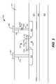
- FIG. 3Ais a cross-sectional view of a first exemplary embodiment of the memory cell of FIG. 2A ;
- FIG. 3Bis a cross-sectional view of a second exemplary embodiment of the memory cell of FIG. 2A ;
- FIG. 3Cis a cross-sectional view of a third exemplary embodiment of the memory cell of FIG. 2A ;
- FIG. 3Dis a cross-sectional view of a fourth exemplary embodiment of the memory cell of FIG. 2A ;
- FIGS. 4A-Dillustrate cross sectional views of a portion of a substrate during fabrication of a single memory level in accordance with this invention.
- FIG. 5is a cross sectional view of a first alternative memory cell provided in accordance with this invention.
- CNT materialshave been shown to exhibit reversible resistivity-switching properties that may be suitable for use in non-volatile memories.
- deposited or grown CNT materialtypically has a rough surface topography, with pronounced thickness variations, such as numerous peaks and valleys. These thickness variations make CNT materials difficult to etch without excessive etching of the underlying substrate, increasing fabrication costs and complexity associated with their use in integrated circuits.
- CMOS transistorsmay be used within a memory cell without being etched.
- a memory cellincludes a CNT reversible resistivity-switching material formed by depositing a CNT seeding layer, patterning and etching the CNT seeding layer, and selectively fabricating CNT material on the patterned and etched CNT seeding layer.
- the CNT seeding layermay be a layer that facilitates CNT formation, such as (1) a single layer of roughened metal nitride, such as surface roughened titanium or tantalum nitride, (2) a multi-layer structure formed from a smooth or surface roughened metal nitride coated with a metal catalyst, (3) a single layer of a metal catalyst such as nickel, cobalt, iron, etc., or (4) a non-metal silicon-germanium (“Si/Ge”) seed layer. Selective formation of CNT material on the CNT seeding layer can eliminate or minimize the need to etch the CNT material.
- Exemplary CNT seeding layersinclude titanium nitride, tantalum nitride, nickel, cobalt, iron or the like, or a non-metal Si/Ge seed layer.
- a titanium or tantalum nitride layermay be surface roughened for use as a CNT seeding layer. Such surface roughened titanium or tantalum nitride may itself serve as a CNT seeding layer.
- the surface roughened titanium or tantalum nitride layermay be coated with an additional conducting layer to facilitate CNT material formation.
- Such a conducting layermay be patterned and etched with the titanium or tantalum nitride layer, or selectively deposited on the titanium or tantalum nitride layer after the titanium or tantalum nitride layer is patterned and etched.
- Exemplary conducting layersinclude nickel, cobalt, iron, etc.
- CNT materialrefers to material that includes one or more single and/or multi-wall CNTs.
- the individual tubes of the CNT materialmay be vertically aligned. Vertically aligned CNTs allow vertical current flow with little or no lateral conduction.
- the individual tubes of the CNT materialmay be fabricated to be substantially vertically aligned to reduce or prevent the formation of lateral or bridging conduction paths between adjacent memory cells. This vertical alignment reduces and/or prevents the state of a memory cell from being influenced or “disturbed” by the state and/or programming of adjacent memory cells. Note that individual tube isolation may or may not extend over the entire thickness of the CNT material.
- some or most of the individual tubesmay be vertically aligned and separated. However, as the individual tubes increase in length vertically, portions of the tubes may come in contact with one another, and even become entangled or entwined. Exemplary techniques for forming CNT materials are described below.
- FIG. 1is a schematic illustration of an exemplary memory cell 100 provided in accordance with the present invention.
- Memory cell 100includes a reversible resistance-switching element 102 coupled to a steering element 104 .
- Reversible resistance-switching element 102includes a reversible resistivity-switching material (not separately shown) having a resistivity that may be reversibly switched between two or more states.
- the reversible resistivity-switching material of element 102may be in an initial, low-resistivity state upon fabrication. Upon application of a first voltage and/or current, the material is switchable to a high-resistivity state. Application of a second voltage and/or current may return the reversible resistivity-switching material to a low-resistivity state.
- reversible resistance-switching element 102may be in an initial, high-resistance state upon fabrication that is reversibly switchable to a low-resistance state upon application of the appropriate voltage(s) and/or current(s).
- one resistance stateWhen used in a memory cell, one resistance state may represent a binary “0,” and another resistance state may represent a binary “1”, although more than two data/resistance states may be used.
- Numerous reversible resistivity-switching materials and operation of memory cells employing reversible resistance-switching elementsare described, for example, in U.S. patent application Ser. No. 11/125,939, filed May 9, 2005 and titled “Rewriteable Memory Cell Comprising A Diode And A Resistance-Switching Material,” which is hereby incorporated by reference herein in its entirety for all purposes.
- reversible resistance-switching element 102is formed using a selectively deposited or grown CNT material. As will be described further below, use of a selectively formed CNT material eliminates the need to etch the CNT material. Fabrication of reversible resistance-switching element 102 thereby is simplified. In the remaining discussion, reversible resistance-switching element 102 will also be referred to as CNT element 102 .
- Steering element 104may include a thin film transistor, a diode, or another suitable steering element that exhibits non-ohmic conduction by selectively limiting the voltage across and/or the current flow through the reversible resistance-switching element 102 .
- memory cell 100may be used as part of a two or three dimensional memory array and data may be written to and/or read from memory cell 100 without affecting the state of other memory cells in the array.
- Memory cell 100operates based on a bi-stable resistance change in CNT element 102 with the application of high programming voltage (e.g., greater than about 4 V). Current through memory cell 100 is modulated by the resistance of CNT element 102 . Memory cell 100 may be read at a voltage lower than the programming voltage that will not change the resistance of CNT element 102 . The difference in resistivities between the two states is over 100 ⁇ , as described in Rueckes, et al. U.S. Pat. No. 6,706,402, which is hereby incorporated herein by reference in its entirety for all purposes.
- Exemplary embodiments of memory cell 100 , reversible resistance-switching element 102 and steering element 104are described below with reference to FIGS. 2A-5 .
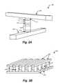
- FIG. 2Ais a simplified perspective view of a first embodiment of a memory cell 200 provided in accordance with the present invention.
- memory cell 200includes a reversible resistance-switching element 202 coupled in series with a diode 204 between a first conductor 206 and a second conductor 208 .
- a barrier layer 210 , a conductive layer 212 and/or a CNT seeding layer 214may be formed between reversible resistance-switching element 202 and diode 204 .
- barrier layer 210may include titanium nitride, tantalum nitride, tungsten nitride, etc.
- conductive layer 212may include tungsten or another suitable metal layer.
- CNT seeding layer 214may be a conducting layer that promotes CNT material formation, such as titanium nitride, tantalum nitride, nickel, cobalt, iron or the like.
- CNT seeding layer 214may be titanium or tantalum nitride with a surface roughened by chemical mechanical polishing (“CMP”) or another suitable process.
- CMPchemical mechanical polishing
- a surface roughened or smooth titanium nitride, tantalum nitride or similar layermay be coated with a metal catalyst layer of nickel, cobalt, iron, etc., that promotes CNT material formation.
- CNT seeding layer 214may simply be a metal catalyst layer such as nickel, cobalt, iron or the like.
- CNT seeding layer 214may be a non-metal Si/Ge layer that promotes CNT formation.
- barrier layer 210may serve as a hard mask during formation of diode 204 .
- metal hard masksare described, for example, in U.S. patent application Ser. No. 11/444,936, filed May 13, 2006 and titled “Conductive Hard Mask To Protect Patterned Features During Trench Etch” (hereinafter “the '936 Application”) which is hereby incorporated by reference herein in its entirety for all purposes.
- An additional barrier layer 216such as titanium nitride, tantalum nitride, tungsten nitride, etc., also may be formed between diode 204 and first conductor 206 .
- CNT seeding layer 214with conductive layer 212 , barrier layer 210 , diode 204 and/barrier layer 216 simplifies fabrication of memory cell 200 as additional patterning and etch steps are not required for CNT seeding layer 214 . Further, CNT material will selectively (e.g., only) form on the patterned and etched CNT seeding layer 214 so that etching of CNT material is not required. This selectively formed CNT material serves as reversible resistance-switching element 202 .
- only a portion, such as one or more filaments, of the CNT material that forms reversible resistance-switching element 202may switch and/or be switchable.
- Diode 204may include any suitable diode such as a vertical polycrystalline p-n or p-i-n diode, whether upward pointing with an n-region above a p-region of the diode or downward pointing with a p-region above an n-region of the diode. Exemplary embodiments of diode 204 are described below with reference to FIG. 3A-C .
- First and/or second conductor 206 , 208may include any suitable conductive material such as tungsten, any appropriate metal, heavily doped semiconductor material, a conductive silicide, a conductive silicide-germanide, a conductive germanide, or the like.
- first and second conductors 206 , 208are rail-shaped and extend in different directions (e.g., substantially perpendicular to one another). Other conductor shapes and/or configurations may be used.
- barrier layers, adhesion layers, antireflection coatings and/or the likemay be used with first and/or second conductors 206 to improve device performance and/or aid in device fabrication.
- FIG. 2Bis a simplified perspective view of a portion of a memory array 218 formed from a plurality of memory cells 200 of FIG. 2A .
- reversible resistance-switching element 202CNT seeding layer 214 , diode 204 , barrier layers 210 and 216 and conductive layer 212 are not separately shown.
- Memory array 218is a “cross-point” array including a plurality of bit lines (second conductors 208 ) and word lines (first conductors 206 ) to which multiple memory cells are coupled (as shown).
- Other memory array configurationsmay be used, as may multiple levels of memory. For example, FIG.
- each memory level 222 , 224includes a plurality of memory cells 200 in a cross-point array.
- additional layerse.g., an interlevel dielectric
- FIG. 2COther memory array configurations may be used, as may additional levels of memory.
- all diodesmay “point” in the same direction, such as upward or downward depending on whether p-i-n diodes having a p-doped region on the bottom or top of the diodes are employed, simplifying diode fabrication.
- the memory levelsmay be formed, as described, for example, in U.S. Pat. No. 6,952,030, “High-density three-dimensional memory cell” which is hereby incorporated by reference herein in its entirety for all purposes.
- the upper conductors of a first memory levelmay be used as the lower conductors of a second memory level that is positioned above the first memory level as shown in FIG. 2D .
- the diodes on adjacent memory levelspreferably point in opposite directions as described in U.S. patent application Ser. No. 11/692,151, filed Mar.
- first memory level 222may be upward pointing diodes as indicated by arrow A 1 (e.g., with p regions at the bottom of the diodes), whereas the diodes of second memory level 224 may be downward pointing diodes as indicated by arrow A 2 (e.g., with n regions at the bottom of the diodes), or vice versa.
- a monolithic three dimensional memory arrayis one in which multiple memory levels are formed above a single substrate, such as a wafer, with no intervening substrates.
- the layers forming one memory levelare deposited or grown directly over the layers of an existing level or levels.
- stacked memorieshave been constructed by forming memory levels on separate substrates and adhering the memory levels atop each other, as in Leedy, U.S. Pat. No. 5,915,167, “Three dimensional structure memory.”
- the substratesmay be thinned or removed from the memory levels before bonding, but as the memory levels are initially formed over separate substrates, such memories are not true monolithic three dimensional memory arrays.
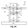
- FIG. 3Ais a cross-sectional view of a first exemplary embodiment of memory cell 200 of FIG. 2A .
- memory cell 200includes reversible resistance-switching element 202 , diode 204 and first and second conductors 206 , 208 .
- diode 204may be a vertical p-n or p-i-n diode, which may either point upward or downward.
- adjacent memory levelspreferably have diodes that point in opposite directions such as downward-pointing p-i-n diodes for a first memory level and upward-pointing p-i-n diodes for an adjacent, second memory level (or vice versa).
- diode 204may be formed from a polycrystalline semiconductor material such as polysilicon, a polycrystalline silicon-germanium alloy, polygermanium or any other suitable material.
- diode 204may include a heavily doped n+ polysilicon region 302 , a lightly doped or an intrinsic (unintentionally doped) polysilicon region 304 above n+ polysilicon region 302 and a heavily doped, p+ polysilicon region 306 above intrinsic region 304 .
- a thin germanium and/or silicon-germanium alloy layermay be formed on n+ polysilicon region 302 to prevent and/or reduce dopant migration from n+ polysilicon region 302 into intrinsic region 304 .
- a barrier layer 308such as titanium nitride, tantalum nitride, tungsten nitride, etc., may be formed between first conductor 206 and n+ region 302 (e.g., to prevent and/or reduce migration of metal atoms into the polysilicon regions).
- a silicide layer 310may be formed on diode 204 to place the deposited silicon in a low resistivity state, as fabricated.
- a low resistivity stateallows for easier programming of memory cell 200 , as a large voltage is not required to switch the deposited silicon to a low resistivity state.
- a silicide-forming metal layer 312such as titanium or cobalt may be deposited on p+ polysilicon region 306 .
- silicide-forming metal layer 312 and the deposited silicon of diode 204interact to form silicide layer 310 , consuming all or a portion of silicide-forming metal layer 312 .
- silicide-forming materialssuch as titanium and/or cobalt react with deposited silicon during annealing to form a silicide layer.
- silicide layers 310enhances the crystalline structure of silicon diode 204 during annealing.
- Lower resistivity siliconthereby is provided. Similar results may be achieved for silicon-germanium alloy and/or germanium diodes.
- reversible resistance-switching element 202is formed by a selective fabrication process in which CNT material is formed on a patterned and etched CNT seeding layer 314 .
- CNT seeding layer 314may be (1) a single layer of roughened metal nitride, such as surface roughened titanium or tantalum nitride, (2) a multi-layer structure formed from a smooth or surface roughened metal nitride coated with a metal catalyst, (3) a single layer of a metal catalyst such as nickel, cobalt, iron, etc., or (4) a non-metal Si/Ge seed layer.
- Exemplary CNT seeding layer materialsinclude titanium or tantalum nitride and/or nickel, cobalt, iron or another suitable metal and/or catalyst, or a non-metal Si/Ge material.
- CNT seeding layer 314 and reversible resistance-switching element 202may be formed over conductive silicide-forming metal layer 312 .
- CNT seeding layer 314 and silicide-forming metal layer 312may be patterned and etched during formation of diode 204 as described below with reference to FIGS. 4A-4D .
- a metal hard maskmay be formed over silicide-forming metal layer 312 prior to formation of CNT seeding layer 314 and resistance-switching element 202 .
- a barrier layer 316 and/or a conductive layer 318may be formed over silicide-forming metal layer 312 .
- CNT seeding layer 314then may be formed over conductive layer 318 .
- Barrier layer 316may include titanium nitride, tantalum nitride, tungsten nitride, etc.
- conductive layer 318may include tungsten or another suitable metal layer.
- barrier layer 316 and/or conductive layer 318may serve as a hard mask during formation of diode 204 and may mitigate any overetching that may occur during formation of top conductor 208 (as described in the '936 Application, previously incorporated).
- CNT seeding layer 314 , barrier layer 316 and conductive layer 318may be patterned and etched, and then serve as a mask during etching of diode 204 .
- Etching of CNT seeding layer 314 , conductive layer 318 , barrier layer 316 , silicide-forming metal layer 312 , diode 204 (p+ polysilicon layer 306 , intrinsic layer 304 , n+ polysilicon layer 302 ) and barrier layer 308creates a pillar structure 320 .
- Dielectric material 322is deposited on top of and around pillar structure 320 to isolate pillar structure 320 from other similar pillar structures of other memory cells (not shown) fabricated on a memory level that includes memory cell 200 .
- a CMP or dielectric etchback stepthen is performed to planarize the dielectric material 322 and remove the dielectric material from the top of CNT seeding layer 314 .
- CNT seeding layer 314may be about 1000 to about 5000 angstroms of a metal nitride such as titanium or tantalum nitride with an arithmetic average surface roughness Ra of about 850 to about 4000 angstroms, and more preferably about 4000 angstroms. In some embodiments, about 1 to about 200 angstroms, and more preferably about 20 angstroms or less, of a metal catalyst layer such as nickel, cobalt, iron, etc., may be deposited onto the surface roughened metal nitride layer prior to CNT formation.
- a metal nitridesuch as titanium or tantalum nitride with an arithmetic average surface roughness Ra of about 850 to about 4000 angstroms, and more preferably about 4000 angstroms.
- a metal catalyst layersuch as nickel, cobalt, iron, etc.
- CNT seeding layer 314may include about 20 to about 500 angstroms of non-roughened or smooth titanium, tantalum or similar metal nitride coated with about 1 to about 200 angstroms, and more preferably about 20 angstroms or less, of a metal catalyst layer such as nickel, cobalt, iron, etc.
- the nickel, cobalt, iron or other metal catalyst layer in any embodimentmay be a continuous or non-continuous film.
- CNT seeding layer 314may include about 1 to about 500 angstroms, and more preferably about 5 angstroms to about 19 angstroms of Si/Ge material. Other materials, thicknesses and surface roughnesses may be used.
- CNT fabrication processis performed to selectively grow and/or deposit CNT material 324 on CNT seeding layer 314 .
- CNT material 324serves as reversible resistance-switching element 202 .
- Any suitable methodmay be used to form CNT material on CNT seeding layer 314 .
- CVDchemical vapor deposition
- PECVDplasma-enhanced CVD
- laser vaporizationelectric arc discharge or the like may be employed.
- CNTsmay be formed on a TiN seeding layer by CVD at a temperature of about 675 to 700° C. in xylene, argon, hydrogen and/or ferrocene at a flow rate of about 100 sccm for about 30 minutes. Other temperatures, gases, flow rates and/or growth times may be used.
- CNTsmay be formed on a nickel catalyst layer by CVD at a temperature of about 650° C. in about 20% C 2 H 4 and 80% Argon at a pressure of about 5.5 Torr for about 20 minutes.
- Other temperatures, gases, ratios, pressures and/or growth timesmay be used.
- CNTsmay be formed on a metal catalyst seeding layer such as nickel, cobalt, iron, etc., using PECVD at a temperature of about 600 to 900° C. in about 20% methane, ethylene, acetylene or another hydrocarbon diluted with about 80% argon, hydrogen and/or ammonia using an RF power of about 100-200 Watts for about 8-30 minutes.
- PECVDPECVD at a temperature of about 600 to 900° C. in about 20% methane, ethylene, acetylene or another hydrocarbon diluted with about 80% argon, hydrogen and/or ammonia using an RF power of about 100-200 Watts for about 8-30 minutes.
- Other temperatures, gases, ratios, powers and/or growth timesmay be used.
- CNTsmay be formed on a Si/Ge seeding layer using CVD or PECVD.
- CVDchemical vapor deposition
- PECVDPECVD
- a CVD techniquemay be used with approximately 850° C. for approximately 10 minutes using methane diluted with H 2 gas.
- Other carbon precursorsmight be used to form CNTs as well.
- CNT material 324forms only over CNT seeding layer 314 of pillar structure 320 (and other similar pillar structures (not shown) of other memory cells fabricated on a memory level that includes memory cell 200 ).
- CNT material 324may have a thickness of about 1 nanometers to about 1 micron (and even tens of microns), and more preferably about 10 to about 20 nanometers, although other CNT material thicknesses may be used.
- the density of the individual tubes in CNT material 324may be, for example, about 6.6 ⁇ 10 3 to about 1 ⁇ 10 6 CNTs/micron 2 , and more preferably at least about 6.6 ⁇ 10 4 CNTs/micron 2 , although other densities may be used.
- the pillar structure 320has a width of about 45 nanometers, in some embodiments, it is preferred to have at least about 10 CNTs, and more preferably at least about 100 CNTs, in CNT material 324 (although fewer CNTs, such as 1, 2, 3, 4, 5, etc., or more CNTs, such as more than 100, may be employed).
- CNT material 324it may be preferable that at least about 50%, and more preferably at least about 2 ⁇ 3, of the carbon nano-tubes of CNT material 324 are semiconducting.
- Multiple wall CNTsare generally metallic, while single wall CNTs may be metallic or semiconducting.
- the individual tubes of CNT material 324may be fabricated to be substantially vertically aligned (e.g., thereby reducing and/or preventing the state of a memory cell from being influenced or “disturbed” by the state and/or programming of adjacent memory cells). Note that this vertical alignment may or may not extend over the entire thickness of CNT material 324 . For example, during the initial growth phase, some or most of the individual tubes may be vertical aligned (e.g., not touching). However, as the individual tubes increase in length vertically, portions of the tubes may come in contact with one another, and even become entangled or entwined.
- defectsmay be intentionally created in the CNT material 324 to improve or otherwise tune the reversible resistivity-switching characteristics of CNT material 324 .
- argon, O 2 or another speciesmay be implanted into CNT material 324 to create defects in CNT material 324 .
- CNT material 324may be subjected or exposed to an argon or O 2 plasma (biased or chemical) to intentionally create defects in CNT material 324 .
- an anneal stepmay be performed prior to depositing dielectric material.
- the annealmay be performed in a vacuum or the presence of one or more forming gases, at a temperature in the range from about 350° C. to about 900° C., for about 30 to about 180 minutes.
- the annealpreferably is performed in about an 80% (N 2 ):20% (H 2 ) mixture of forming gases, at about 625° C. for about one hour.
- Suitable forming gasesmay include one or more of N 2 , Ar, and H 2 , whereas preferred forming gases may include a mixture having above about 75% N 2 or Ar and below about 25% H 2 .
- a vacuummay be used.
- Suitable temperaturesmay range from about 350° C. to about 900° C., whereas preferred temperatures may range from about 585° C. to about 675° C.
- Suitable durationsmay range from about 0.5 hour to about 3 hours, whereas preferred durations may range from about 1 hour to about 1.5 hours.
- Suitable pressuresmay range from about 1 mT to about 760T, whereas preferred pressures may range from about 300 mT to about 600 mT.
- a queue time of preferably about 2 hours between the anneal and the dielectric depositionpreferably accompanies the use of the anneal.
- a ramp up durationmay range from about 0.2 hours to about 1.2 hours and preferably is between about 0.5 hours and 0.8 hours.
- a ramp down durationalso may range from about 0.2 hours to about 1.2 hours and preferably is between about 0.5 hours and 0.8 hours.
- CNT materialmay absorb water from the air over time. Likewise, it is believed that the moisture may increase the likelihood of de-lamination of the CNT material. In some cases, it also might be acceptable to have a que time of 2 hours from the time of CNT growth to dielectric deposition, skipping the anneal altogether.
- incorporación of such a post-CNT-formation-annealpreferably takes into account other layers present on the device that includes the CNT material, because these other layers will also be subject to the anneal.
- the annealmay be omitted or its parameters may be adjusted where the aforementioned preferred anneal parameters would damage the other layers.
- the anneal parametersmay be adjusted within ranges that result in the removal of moisture without damaging the layers of the annealed device.
- the temperaturemay be adjusted to stay within an overall thermal budget of a device being formed.
- any suitable forming gases, temperatures and/or durationsmay be used that are appropriate for a particular device.
- such an annealmay be used with any carbon-based layer or carbon-containing material, such as layers having CNT material, graphite, graphene, amorphous carbon, etc.
- dielectric material 326is deposited on top of and around CNT material 324 to isolate CNT material 324 from other similar CNT material regions of other memory cells (not shown) fabricated on a memory level that includes memory cell 200 .
- a CMP or dielectric etchback stepthen is performed to planarize dielectric material 326 and remove the dielectric material from the top of CNT material 324 .
- top conductor 208is formed.
- one or more barrier layers and/or adhesion layers 328may be formed over CNT material 324 /reversible resistance-switching element 202 prior to deposition of conductive layer 330 .
- Conductive layer 330 and barrier layer 328may be patterned and/or etched together to form top conductor 208 .
- top conductor 208may be formed using a damascene process as described below with reference to FIGS. 4A-4D .
- memory cell 200may be annealed to crystallize the deposited semiconductor material of diode 204 (and/or to form silicide layer 310 ).
- the annealmay be performed for about 10 seconds to about 2 minutes in nitrogen at a temperature of about 600 to 800° C., and more preferably between about 650 and 750° C. Other annealing times, temperatures and/or environments may be used.
- silicide layer 310may serve as a “crystallization template” or “seed” during annealing for underlying deposited semiconductor material that forms diode 204 . Lower resistivity diode material thereby is provided.
- CNT seeding layer 314may include one or more additional layers.
- FIG. 3Bis a cross-sectional view of a second exemplary embodiment of memory cell 200 of FIG. 2A in which CNT seeding layer 314 includes an additional metal catalyst layer 332 .
- Metal catalyst layer 332may be selectively deposited over the CMP or etchback exposed CNT seeding layer 314 .
- a nickel, cobalt, iron, etc., metal catalyst layer 332may be selectively formed over a surface roughened titanium or tantalum nitride CNT seeding layer 314 by electroless deposition, electroplating or the like.
- CNT material 324then may be formed over the metal catalyst coated CNT seeding layer 314 .
- metal catalyst layer 332may eliminate the need for a catalyst precursor during CNT formation.
- Exemplary metal catalyst layer thicknessesrange from about 1 to 200 angstroms, although other thicknesses may be used. Such an embodiment may be used with or without metal hard mask layers 316 and 318 .
- a nickel, cobalt, iron, or similar metal catalyst layeralso may be formed over a non-surface-roughened or smooth titanium nitride, tantalum nitride or similar layer by electroless deposition, electroplating or the like.
- FIG. 3Cis a cross-sectional view of a third exemplary embodiment of memory cell 200 of FIG. 2A .
- Memory cell 200 of FIG. 3Cis similar to memory cell 200 of FIG. 3B , but does not include surface roughened CNT seeding layer 314 .
- no CNT seeding layer 314is deposited over conductive layer 318 prior to formation of pillar structure 320 .
- dielectric material 322is deposited on top of and around pillar structure 320 and planarized to expose the top of conductive layer 318 .
- a metal catalyst layer 332such as nickel, cobalt, iron, etc., then is selectively deposited on the exposed conductive layer 318 , and CNT material 324 may be formed over metal catalyst layer 332 .
- CNT material 324may be formed over metal catalyst layer 332 .
- such an embodimentmay be used with or without metal hard mask layers 316 and 318 .
- FIG. 3Dis a cross-sectional view of a fourth exemplary embodiment of memory cell 200 of FIG. 2A .
- Memory cell 200 of FIG. 3Dis similar to memory cell 200 of FIG. 3A , but includes a non-metal Si/Ge CNT seeding layer 314 ′.
- Using a non-metal Si/Ge seedhas the advantage that silicon and germanium materials are compatible with conventional semiconductor fabrication facility materials, unlike iron-based metal CNT seed materials.
- Si/Ge CNT seeding layer 314 ′may be formed over silicide-forming metal layer 312 .
- CNT seeding layer 314 ′ and silicide-forming metal layer 312may be patterned and etched during formation of diode 204 as described below with reference to FIGS. 4A-4D .
- An oxide layer (not shown) or Si/Ge CNT seeding layer 314 ′may be used as a hard mask for pattern transfer.
- a metal hard maskmay be formed over silicide-forming metal layer 312 prior to formation of CNT seeding layer 314 ′ and resistance-switching element 202 .
- a barrier layer 316 and/or a conductive layer 318may be formed over silicide-forming metal layer 312 .
- CNT seeding layer 314 ′then may be formed over conductive layer 318 .
- Barrier layer 316may include titanium nitride, tantalum nitride, tungsten nitride, etc., and conductive layer 318 may include tungsten or another suitable metal layer.
- barrier layer 316 and/or conductive layer 318 , and CNT seeding layer 314 ′may serve as a hard mask during formation of diode 204 and may mitigate any overetching that may occur during formation of top conductor 208 (as described in the '936 Application, previously incorporated).
- CNT seeding layer 314 ′, barrier layer 316 and conductive layer 318may be patterned and etched, and then serve as a mask during etching of diode 204 .
- Etching of CNT seeding layer 314 ′, conductive layer 318 , barrier layer 316 , silicide-forming metal layer 312 , diode 204 (p+ polysilicon layer 306 , intrinsic layer 304 , n+ polysilicon layer 302 ) and barrier layer 308creates a pillar structure 320 .
- Dielectric material 322is deposited on top of and around pillar structure 320 to isolate pillar structure 320 from other similar pillar structures of other memory cells (not shown) fabricated on a memory level that includes memory cell 200 .
- a CMP or dielectric etchback stepthen is performed to planarize the dielectric material 322 and remove the dielectric material from the top of CNT seeding layer 314 ′.
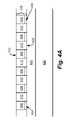
- FIGS. 4A-Dillustrate cross sectional views of a portion of a substrate 400 during fabrication of a first memory level in accordance with the present invention.
- the first memory levelincludes a plurality of memory cells that each include a reversible resistance-switching element formed by selectively fabricating CNT material above a substrate. Additional memory levels may be fabricated above the first memory level (as described previously with reference to FIGS. 2C-2D ).
- substrate 400is shown as having already undergone several processing steps.
- Substrate 400may be any suitable substrate such as a silicon, germanium, silicon-germanium, undoped, doped, bulk, silicon-on-insulator or other substrate with or without additional circuitry.
- substrate 400may include one or more n-well or p-well regions (not shown).
- Isolation layer 402is formed above substrate 400 .
- isolation layer 402may be a layer of silicon dioxide, silicon nitride, silicon oxynitride or any other suitable insulating layer.
- adhesion layer 404is formed over isolation layer 402 (e.g., by physical vapor deposition or another method).
- adhesion layer 404may be about 20 to about 500 angstroms, and preferably about 100 angstroms, of titanium nitride or another suitable adhesion layer such as tantalum nitride, tungsten nitride, combinations of one or more adhesion layers, or the like. Other adhesion layer materials and/or thicknesses may be employed. In some embodiments, the adhesion layer 404 may be optional.
- Conductive layer 406may include any suitable conductive material such as tungsten or another appropriate metal, heavily doped semiconductor material, a conductive silicide, a conductive silicide-germanide, a conductive germanide, or the like deposited by any suitable method (e.g., CVD, physical vapor deposition (“PVD”), etc.). In at least one embodiment, conductive layer 406 may comprise about 200 to about 2500 angstroms of tungsten. Other conductive layer materials and/or thicknesses may be used.
- adhesion layer 404 and conductive layer 406are patterned and etched.
- adhesion layer 404 and conductive layer 406may be patterned and etched using conventional lithography techniques, with a soft or hard mask, and wet or dry etch processing.
- adhesion layer 404 and conductive layer 406are patterned and etched to form substantially parallel, substantially co-planar conductors 408 (as shown in FIG. 4A ).
- Exemplary widths for conductors 408 and/or spacings between conductors 408range from about 200 to about 2500 angstroms, although other conductor widths and/or spacings may be used.
- a dielectric layer 410is formed over substrate 400 to fill the voids between conductors 408 .
- a dielectric layer 410is formed over substrate 400 to fill the voids between conductors 408 .
- approximately 3000-7000 angstroms of silicon dioxidemay be deposited on substrate 400 and planarized using chemical mechanical polishing or an etchback process to form a planar surface 412 .
- Planar surface 412includes exposed top surfaces of conductors 408 separated by dielectric material (as shown).
- dielectric materialsuch as silicon nitride, silicon oxynitride, low K dielectrics, etc., and/or other dielectric layer thicknesses may be used.
- Exemplary low K dielectricsinclude carbon doped oxides, silicon carbon layers, or the like.
- conductors 408may be formed using a damascene process in which dielectric layer 410 is formed, patterned and etched to create openings or voids for conductors 408 .
- the openings or voidsthen may be filled with adhesion layer 404 and conductive layer 406 (and/or a conductive seed, conductive fill and/or barrier layer if needed).
- Adhesion layer 404 and conductive layer 406then may be planarized to form planar surface 412 . In such an embodiment, adhesion layer 404 will line the bottom and sidewalls of each opening or void.
- barrier layer 414is formed over planarized top surface 412 of substrate 400 .
- Barrier layer 414may be about 20 to about 500 angstroms, and preferably about 100 angstroms, of titanium nitride or another suitable barrier layer such as tantalum nitride, tungsten nitride, combinations of one or more barrier layers, barrier layers in combination with other layers such as titanium/titanium nitride, tantalum/tantalum nitride or tungsten/tungsten nitride stacks, or the like. Other barrier layer materials and/or thicknesses may be employed.
- each diodemay be a vertical p-n or p-i-n diode as previously described.
- each diodeis formed from a polycrystalline semiconductor material such as polysilicon, a polycrystalline silicon-germanium alloy, polygermanium or any other suitable material. For convenience, formation of a polysilicon, downward-pointing diode is described herein. It will be understood that other materials and/or diode configurations may be used.
- n+ silicon layer 416is deposited on barrier layer 414 .
- n+ silicon layer 416is in an amorphous state as deposited.
- n+ silicon layer 416is in a polycrystalline state as deposited.
- CVD or another suitable processmay be employed to deposit n+ silicon layer 416 .
- n+ silicon layer 416may be formed, for example, from about 100 to about 1000 angstroms, preferably about 100 angstroms, of phosphorus or arsenic doped silicon having a doping concentration of about 10 21 cm ⁇ 3 . Other layer thicknesses, doping types and/or doping concentrations may be used.
- N+ silicon layer 416may be doped in situ, for example, by flowing a donor gas during deposition. Other doping methods may be used (e.g., implantation).
- a lightly doped, intrinsic and/or unintentionally doped silicon layer 418is formed over n+ silicon layer 416 .
- intrinsic silicon layer 418is in an amorphous state as deposited. In other embodiments, intrinsic silicon layer 418 is in a polycrystalline state as deposited. CVD or another suitable deposition method may be employed to deposit intrinsic silicon layer 418 .
- intrinsic silicon layer 418may be about 500 to about 4800 angstroms, preferably about 2500 angstroms, in thickness. Other intrinsic layer thicknesses may be used.
- a thin (e.g., a few hundred angstroms or less) germanium and/or silicon-germanium alloy layermay be formed on n+ silicon layer 416 prior to deposition of intrinsic silicon layer 418 to prevent and/or reduce dopant migration from n+ silicon layer 416 into intrinsic silicon layer 418 (as described in the '331 Application, previously incorporated).
- Heavily doped, p-type siliconis either deposited and doped by ion implantation or is doped in situ during deposition to form a p+ silicon layer 420 .
- a blanket p+ implantmay be employed to implant boron a predetermined depth within intrinsic silicon layer 418 .
- Exemplary implantable molecular ionsinclude BF 2 , BF 3 , B and the like.
- an implant dose of about 1-5 ⁇ 10 15 ions/cm 2may be employed.
- Other implant species and/or dosesmay be used.
- a diffusion processmay be employed.
- the resultant p+ silicon layer 420has a thickness of about 100-700 angstroms, although other p+ silicon layer sizes may be used.
- silicide-forming metal layer 422is deposited over p+ silicon layer 420 .
- exemplary silicide-forming metalsinclude sputter or otherwise deposited titanium or cobalt.
- silicide-forming metal layer 422has a thickness of about 10 to about 200 angstroms, preferably about 20 to about 50 angstroms and more preferably about 20 angstroms. Other silicide-forming metal layer materials and/or thicknesses may be used.
- a barrier layer 424is deposited over silicide-forming metal layer 422 .
- Barrier layer 424may be about 20 to about 500 angstroms, and preferably about 100 angstroms, of titanium nitride or another suitable barrier layer such as tantalum nitride, tungsten nitride, combinations of one or more barrier layers, barrier layers in combination with other layers such as titanium/titanium nitride, tantalum/tantalum nitride or tungsten/tungsten nitride stacks, or the like. Other barrier layer materials and/or thicknesses may be employed.
- Conductive layer 426may be about 50 to about 1000 angstroms, and preferably about 500 angstroms of conductive material such as tungsten or another suitable metal.
- CNT seeding layer 427is formed over conductive layer 426 .
- CNT seeding layer 427may be about 1000 to about 5000 angstroms of titanium or tantalum nitride, although other thicknesses may be used.
- CNT seeding layer 427may be about 1 to about 500 angstroms of Si/Ge, although other thicknesses may be used.
- the Si/Ge layermay be formed on conductive layer 426 by CVD, PECVD, or other similar processing techniques.
- a silicon seed layermay be formed over conductive layer 426 , and germanium nano-islands may be selectively grown onto the silicon seed layer, such as by CVD.
- Selective germanium depositionmay be performed using low pressure CVD techniques at approximately 500° C. and 100 mT with GeH 4 .
- a carbon implantwith dose of approximately 3 ⁇ 10 16 cm ⁇ 2 and energy of approximately 30 KeV may be used.
- the surfacemay be treated with an approximately 30% H 2 O 2 solution which results in a GeO or SiO growth of approximately 5 angstroms to approximately 19 angstroms.
- Barrier layer 414 , silicon regions 416 , 418 , and 420 , silicide-forming metal layer 422 , barrier layer 424 , conductive layer 426 and CNT seeding layer 427are then patterned and etched into pillars 428 .
- CNT seeding layer 427 , conductive layer 426 and barrier layer 424are etched. The etch continues, etching silicide-forming metal layer 422 , silicon regions 420 , 418 , and 416 and barrier layer 414 .
- CNT seeding layer 427 , conductive layer 426 and barrier layer 414serve as a hard mask during the silicon etch.
- a hard maskis an etched layer which serves to pattern the etch of an underlying layer; if all of the photoresist present on CNT seeding layer 427 has been consumed, the hard mask can provide the pattern in its stead.
- pillars 428are formed in a single photolithographic step. Conventional lithography techniques, and wet or dry etch processing may be employed to form pillars 428 .
- Each pillar 428includes a p-i-n, downward-pointing diode 430 . Upward-pointing p-i-n diodes may be similarly formed.
- a dielectric layer 432is deposited over pillars 428 to fill the voids between pillars 428 .
- a dielectric layer 432For example, approximately 200-7000 angstroms of silicon dioxide may be deposited and planarized using chemical mechanical polishing or an etchback process to form a planar surface 434 .
- Planar surface 434includes exposed top surfaces of pillars 428 separated by dielectric material 432 (as shown).
- Other dielectric materialssuch as silicon nitride, silicon oxynitride, low K dielectrics, etc., and/or other dielectric layer thicknesses may be used. Exemplary low K dielectrics include carbon doped oxides, silicon carbon layers, or the like.
- CMPmay be used to expose CNT seeding layer 427 . If CNT seeding layer 427 is a Si/Ge seed layer, after the polish, the Si/Ge layer may be about 50 nm thick with an approximately 70% Si and approximately 30% Ge composition.
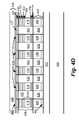
- CNT material 436( FIG. 4C ) is selectively formed on CNT seeding layer 427 of each pillar 428 .
- CNT seeding layer 427is titanium nitride, tantalum nitride or a similar material
- the surface of CNT seeding layer 427may be roughened to allow CNTs to be formed directly on CNT seeding layer 427 . See, e.g., the Smith Article and the Rao Article, referenced above.
- CNT seeding layer 427may be roughened to have an arithmetic average surface roughness Ra of at least about 850 to 4000 angstroms, and more preferably at least about 4000 angstroms. Other surface roughnesses may be employed.
- an additional metal catalyst/seeding layersuch as nickel, cobalt, iron, etc., may be selectively deposited over a surface-roughened CNT seeding layer 427 prior to formation of CNT material 436 to provide the benefits a metal catalyst during CNT formation (as described previously with reference to FIG. 3B ).
- a metal catalyst layermay be used without an underlying, surface roughened seeding layer (as described previously with reference to FIG. 3C ).
- CNT fabrication processis performed to selectively grow and/or deposit CNT material 436 on each pillar 428 .
- CNT material 436serves as reversible resistance-switching element 202 .
- Any suitable methodmay be used to form CNT material 436 on each pillar 428 .
- CVDchemical vapor deposition
- plasma-enhanced CVDplasma-enhanced CVD
- laser vaporizationelectric arc discharge or the like
- CNTsmay be formed on a TiN seeding layer by CVD at a temperature of about 675 to 700° C. in xylene, argon, hydrogen and/or ferrocene at a flow rate of about 100 sccm for about 30 minutes. Other temperatures, gases, flow rates and/or growth times may be used.
- CNTsmay be formed on a nickel catalyst layer by CVD at a temperature of about 650° C. in about 20% C 2 H 4 and 80% Argon at a pressure of about 5.5 Torr for about 20 minutes.
- Other temperatures, gases, ratios, pressures and/or growth timesmay be used.
- CNTsmay be formed on a metal catalyst layer such as nickel, cobalt, iron, etc., using plasma enhanced CVD at a temperature of about 600 to 900° C. in about 20% methane, ethylene, acetylene or another hydrocarbon diluted with about 80% argon, hydrogen and/or ammonia using an RF power of about 100-200 Watts for about 8-30 minutes.
- a metal catalyst layersuch as nickel, cobalt, iron, etc.
- plasma enhanced CVDat a temperature of about 600 to 900° C. in about 20% methane, ethylene, acetylene or another hydrocarbon diluted with about 80% argon, hydrogen and/or ammonia using an RF power of about 100-200 Watts for about 8-30 minutes.
- RF powerabout 100-200 Watts for about 8-30 minutes.
- Other temperatures, gases, ratios, powers and/or growth timesmay be used.
- CNTsmay be formed on a Si/Ge layer by CVD at a temperature of about 850° C. in methane diluted with H 2 gas for about 10 minutes.
- CNT material 436forms only over CNT seeding layer 427 of each pillar 428 .
- CNT material 436may have a thickness of about 1 nanometers to about 1 micron (and even tens of microns), and more preferably about 10 to about 20 nanometers, although other CNT material thicknesses may be used.
- the density of individual tubes in CNT material 436may be, for example, about 6.6 ⁇ 10 3 to about 1 ⁇ 10 6 CNTs/micron 2 , and more preferably at least about 6.6 ⁇ 10 4 CNTs/micron 2 , although other densities may be used.
- pillars 428have a width of about 45 nanometers, in some embodiments, it is preferred to have at least about 10 CNTs, and more preferably at least about 100 CNTs, in CNT material 436 formed on each pillar 428 (although fewer CNTs, such as 1, 2, 3, 4, 5, etc., or more CNTs, such as more than 100, may be employed).
- dielectric material 437is deposited on top of and around the regions of CNT material 436 to isolate adjacent CNT material regions from one another.
- a CMP or dielectric etchback stepthen is performed to planarize dielectric material 437 and remove the dielectric material from the top of the regions of CNT material 436 .
- silicon dioxidemay be deposited and planarized using chemical mechanical polishing or an etchback process. If the CNTs have been exposed to air for significant amounts of time, a dehydration anneal prior to the dielectric deposition might improve adhesion between the dielectric and the CNT.
- dielectric materialssuch as silicon nitride, silicon oxynitride, low K dielectrics, etc., and/or other dielectric layer thicknesses may be used.
- Exemplary low K dielectricsinclude carbon doped oxides, silicon carbon layers, or the like.
- a second set of conductors 438may be formed above pillars 428 in a manner similar to the formation of the bottom set of conductors 408 .
- one or more barrier layers and/or adhesion layers 440may be deposited over reversible resistance-switching elements 436 prior to deposition of a conductive layer 442 used to form the upper, second set of conductors 438 .
- Conductive layer 442may be formed from any suitable conductive material such as tungsten, another suitable metal, heavily doped semiconductor material, a conductive silicide, a conductive silicide-germanide, a conductive germanide, or the like deposited by any suitable method (e.g., CVD, PVD, etc.). Other conductive layer materials may be used.
- Barrier layers and/or adhesion layers 440may include titanium nitride or another suitable layer such as tantalum nitride, tungsten nitride, combinations of one or more layers, or any other suitable material(s).
- the deposited conductive layer 442 and barrier and/or adhesion layer 440may be patterned and etched to form second set of conductors 438 .
- upper conductors 438are substantially parallel, substantially coplanar conductors that extend in a different direction than lower conductors 408 .
- upper conductors 438may be formed using a damascene process in which a dielectric layer is formed, patterned and etched to create openings or voids for conductors 438 .
- conductive layer 426 and barrier layer 424may mitigate the effects of overetching of such a dielectric layer during formation of the openings or voids for upper conductors 438 , preventing accidental shorting of diodes 430 .
- the openings or voidsmay be filled with adhesion layer 440 and conductive layer 442 (and/or a conductive seed, conductive fill and/or barrier layer if needed).
- Adhesion layer 440 and conductive layer 442then may be planarized to form a planar surface.
- the resultant structuremay be annealed to crystallize the deposited semiconductor material of diodes 430 (and/or to form silicide regions by reaction of silicide-forming metal layer 422 with p+ region 420 ).
- the annealmay be performed for about 10 seconds to about 2 minutes in nitrogen at a temperature of about 600 to 800° C., and more preferably between about 650 and 750° C. Other annealing times, temperatures and/or environments may be used.
- silicide regions formed as each silicide-forming metal layer region 422 and p+ region 420 reactmay serve as “crystallization templates” or “seeds” during annealing for underlying deposited semiconductor material that forms diodes 430 (e.g., changing any amorphous semiconductor material to polycrystalline semiconductor material and/or improving overall crystalline properties of diodes 430 ). Lower resistivity diode material thereby is provided.
- FIG. 5is a cross sectional view of an exemplary memory cell 500 provided in accordance with the present invention.
- Memory cell 500includes a thin film transistor (“TFT”), such as a thin film, metal oxide semiconductor field effect transistor (“MOSFET”) 502 coupled to a reversible resistance-switching element 504 formed above a substrate 505 .
- TFTthin film transistor
- MOSFET 502may be an n-channel or a p-channel thin film MOSFET formed on any suitable substrate.
- an insulating region 506such as silicon dioxide, silicon nitride, oxynitride, etc., is formed above substrate 505 and a deposited semiconductor region 507 such as deposited silicon, germanium, silicon-germanium, etc., is formed above insulating region 506 .
- Thin film MOSFET 502is formed within deposited semiconductor region 507 and is insulated from substrate 505 by the insulating region 506 .
- MOSFET 502includes source/drain regions 508 , 510 and channel region 512 , as well as gate dielectric layer 514 , gate electrode 516 and spacers 518 a - b.
- source/drain regions 508 , 510may be doped p-type and channel region 512 may be doped n-type, wheras in other embodiments source/drain regions 508 , 510 may be doped n-type and channel region 512 may be doped p-type.
- Any other MOSFET configuration or any suitable fabrication techniquesmay be employed for thin film MOSFET 502 .
- MOSFET 502may be electrically isolated by isolation regions (not shown) formed using an STI, LOCOS or other similar process.
- gate, source and/or drain regions of MOSFET 502may be shared with other transistors (not shown) formed on the substrate 505 .
- Reversible resistance-switching element 504includes a reversible resistivity-switching CNT material 522 formed over a conductive plug 526 .
- reversible resistivity-switching CNT material 522is formed using a selective formation process as previously described with reference to the embodiments of FIGS. 1-4D .
- a CNT seeding layer 524such as titanium or tantalum nitride and/or a metal catalyst such as nickel, cobalt, iron, etc., or a Si/Ge layer may be formed over conductive plug 526 .
- CNT material 522then may be selectively formed over CNT seeding layer 524 as previously described.
- reversible resistance-switching element 504is coupled to source/drain region 510 of MOSFET 502 by a first conductive plug 526 and to a first metal level (“M1”) line 528 by a second conductive plug 530 (which extend through a dielectric layer 532 ).
- a third conductive plug 534couples source/drain region 508 of MOSFET 502 to an M1 line 536 .
- the conductive plugs and/or linesmay be formed from any suitable materials (without or without barriers layers) such as tungsten, another metal, heavily doped semiconductor material, a conductive silicide, a conductive silicide-germanide, a conductive germanide, or the like.
- Dielectric layer 532may include any suitable dielectric such as silicon dioxide, silicon nitride, silicon oxynitride, low K dielectrics, etc.
- thin film MOSFET 502operates as a steering element in a manner similar to that of the diodes employed in the memory cells of FIGS. 2A-4D , selectively limiting the voltage applied across and/or the current flow through reversible resistance-switching element 504 .
- This integration schemecan be extended to selectively grow vertically oriented CNT films in series with a TFT as the steering element instead of the vertical pillar diode.
- the TFT steering elementmay be either planar or vertical.
Landscapes
- Engineering & Computer Science (AREA)
- Chemical & Material Sciences (AREA)
- Nanotechnology (AREA)
- Physics & Mathematics (AREA)
- Mathematical Physics (AREA)
- Theoretical Computer Science (AREA)
- Crystallography & Structural Chemistry (AREA)
- Manufacturing & Machinery (AREA)
- Semiconductor Memories (AREA)
Abstract
Description
- This application claims the benefit of U.S. Provisional Patent Application No. 61/044,406, filed Apr. 11, 2008, which is incorporated by reference herein in its entirety for all purposes.
- This application is related to the following patent applications, each of which is hereby incorporated by reference herein in its entirety for all purposes: (1) U.S. patent application Ser. No. ______, filed on even date herewith and titled “Memory Cell That Employs A Selectively Fabricated Carbon Nano-Tube Reversible Resistance-Switching Element Formed Over A Bottom Conductor And Methods Of Forming The Same;” (2) U.S. patent application Ser. No. 11/968,156, filed Dec. 31, 2007 and titled “Memory Cell That Employs A Selectively Fabricated Carbon Nano-Tube Reversible Resistance-Switching Element Formed On A Bottom Conductor And Methods Of Forming The Same;” (3) U.S. patent application Ser. No. 11/968,159, filed Dec. 31, 2007 and titled “Memory Cell With Planarized Carbon Nanotube Layer And Methods Of Forming The Same;” (4) U.S. patent application Ser. No. 11/968,154, filed Dec. 31, 2007 and titled “Memory Cell That Employs A Selectively Fabricated Carbon Nano-Tube Reversible Resistance-Switching Element And Methods Of Forming The Same;” and (5) U.S. Provisional Patent Application Ser. No. 61/044,414, filed Apr. 11, 2008 and titled “Memory Cell That Employs A Selectively Fabricated Carbon Nano-Tube Reversible Resistance-Switching Element Formed Over A Bottom Conductor And Methods Of Forming The Same.”
- The present invention relates to non-volatile memories, and more particularly to a memory cell that employs a selectively fabricated carbon nano-tube (“CNT”) reversible resistance-switching element and methods of forming the same.
- Non-volatile memories formed from reversible resistance-switching elements are known. For example, U.S. patent application Ser. No. 11/968,154, filed Dec. 31, 2007, titled “Memory Cell That Employs A Selectively Fabricated Carbon Nano-Tube Reversible Resistance Switching Element And Methods Of Forming The Same” (the “'154 Application”), which is hereby incorporated by reference herein in its entirety for all purposes, describes a rewriteable non-volatile memory cell that includes a diode coupled in series with a carbon-based reversible resistivity switching material such as carbon.
- However, fabricating memory devices from rewriteable resistivity-switching materials is technically challenging. Improved methods of forming memory devices that employ resistivity-switching materials are desirable.
- In a first aspect of the invention, a method of fabricating a memory cell is provided that includes: (1) fabricating a steering element above a substrate; and (2) fabricating a reversible-resistance switching element coupled to the steering element by: (a) fabricating a CNT seeding layer by depositing a silicon-germanium (“Si/Ge”) layer above the substrate, (b) patterning and etching the CNT seeding layer, and (c) selectively fabricating CNT material on the CNT seeding layer.
- In a second aspect of the invention, a method of fabricating a memory cell is provided that includes: (1) fabricating a first conductor above a substrate; (2) fabricating a reversible-resistance switching element above the first conductor by: (a) fabricating a CNT seeding layer by depositing a Si/Ge layer above the first conductor, (b) patterning and etching the CNT seeding layer, and (c) selectively fabricating CNT material on the CNT seeding layer; (3) fabricating a diode above the first conductor; and (4) fabricating a second conductor above the diode and the reversible resistance-switching element.
- In a third aspect of the invention, a method of fabricating a memory cell is provided that includes: (1) fabricating a thin film transistor having a source region and a drain region; (2) fabricating a first conductor coupled to the source region or the drain region of the transistor; (3) fabricating a reversible-resistance switching element coupled to the first conductor by: (a) fabricating a CNT seeding layer by depositing a Si/Ge layer above the first conductor; (b) patterning and etching the CNT seeding layer; and (c) selectively fabricating CNT material on the CNT seeding layer; (4) fabricating a diode above the first conductor; and (5) fabricating a second conductor above the reversible resistance-switching element.
- In a fourth aspect of the invention, a memory cell is provided that includes: (1) a steering element; (2) a patterned and etched carbon nano-tube (“CNT”) seeding layer comprising silicon-germanium; and (3) a reversible resistance-switching element coupled to the steering element and including CNT material selectively fabricated on the CNT seeding layer.
- In a fifth aspect of the invention, a memory cell is provided that includes: (1) a first conductor; (2) a second conductor formed above the first conductor; (3) a diode formed between the first and second conductors; and (4) a CNT seeding layer comprising Si/Ge between the first and second conductors; and (5) a reversible resistance-switching element including CNT material selectively fabricated on the CNT seeding layer.
- In a sixth aspect of the invention, a memory cell is provided that includes: (1) a thin film transistor having a source region and a drain region; (2) a first conductor coupled to the source region or the drain region; (3) a CNT seeding layer comprising Si/Ge fabricated above the first conductor; (4) a reversible resistance-switching element including CNT material selectively fabricated on the CNT seeding layer; and (5) a second conductor formed above the reversible resistance-switching element. Numerous other aspects are provided in accordance with these and other embodiments of the invention.
- Other features and aspects of the present invention will become more fully apparent from the following detailed description, the appended claims and the accompanying drawings.
- Features of the present invention can be more clearly understood from the following detailed description considered in conjunction with the following drawings, in which the same reference numerals denote the same elements throughout, and in which:
FIG. 1 is a schematic illustration of an exemplary memory cell provided in accordance with this invention;FIG. 2A is a simplified perspective view of a first embodiment of a memory cell provided in accordance with this invention;FIG. 2B is a simplified perspective view of a portion of a first memory level formed from a plurality of the memory cells ofFIG. 2A ;FIG. 2C is a simplified perspective view of a portion of a first exemplary three dimensional memory array provided in accordance with this invention;FIG. 2D is a simplified perspective view of a portion of a second exemplary three dimensional memory array provided in accordance with this invention;FIG. 3A is a cross-sectional view of a first exemplary embodiment of the memory cell ofFIG. 2A ;FIG. 3B is a cross-sectional view of a second exemplary embodiment of the memory cell ofFIG. 2A ;FIG. 3C is a cross-sectional view of a third exemplary embodiment of the memory cell ofFIG. 2A ;FIG. 3D is a cross-sectional view of a fourth exemplary embodiment of the memory cell ofFIG. 2A ;FIGS. 4A-D illustrate cross sectional views of a portion of a substrate during fabrication of a single memory level in accordance with this invention; andFIG. 5 is a cross sectional view of a first alternative memory cell provided in accordance with this invention.- Some CNT materials have been shown to exhibit reversible resistivity-switching properties that may be suitable for use in non-volatile memories. However, deposited or grown CNT material typically has a rough surface topography, with pronounced thickness variations, such as numerous peaks and valleys. These thickness variations make CNT materials difficult to etch without excessive etching of the underlying substrate, increasing fabrication costs and complexity associated with their use in integrated circuits.
- In accordance with the present invention, difficult-to-etch, CNT rewriteable resistivity-switching materials may be used within a memory cell without being etched. For example, in at least one embodiment, a memory cell is provided that includes a CNT reversible resistivity-switching material formed by depositing a CNT seeding layer, patterning and etching the CNT seeding layer, and selectively fabricating CNT material on the patterned and etched CNT seeding layer. The CNT seeding layer may be a layer that facilitates CNT formation, such as (1) a single layer of roughened metal nitride, such as surface roughened titanium or tantalum nitride, (2) a multi-layer structure formed from a smooth or surface roughened metal nitride coated with a metal catalyst, (3) a single layer of a metal catalyst such as nickel, cobalt, iron, etc., or (4) a non-metal silicon-germanium (“Si/Ge”) seed layer. Selective formation of CNT material on the CNT seeding layer can eliminate or minimize the need to etch the CNT material.
- Exemplary CNT seeding layers include titanium nitride, tantalum nitride, nickel, cobalt, iron or the like, or a non-metal Si/Ge seed layer. In some embodiments, a titanium or tantalum nitride layer may be surface roughened for use as a CNT seeding layer. Such surface roughened titanium or tantalum nitride may itself serve as a CNT seeding layer. In other embodiments, the surface roughened titanium or tantalum nitride layer may be coated with an additional conducting layer to facilitate CNT material formation. Such a conducting layer may be patterned and etched with the titanium or tantalum nitride layer, or selectively deposited on the titanium or tantalum nitride layer after the titanium or tantalum nitride layer is patterned and etched. Exemplary conducting layers include nickel, cobalt, iron, etc.
- As used herein, CNT material refers to material that includes one or more single and/or multi-wall CNTs. In some embodiments, the individual tubes of the CNT material may be vertically aligned. Vertically aligned CNTs allow vertical current flow with little or no lateral conduction. In some embodiments, the individual tubes of the CNT material may be fabricated to be substantially vertically aligned to reduce or prevent the formation of lateral or bridging conduction paths between adjacent memory cells. This vertical alignment reduces and/or prevents the state of a memory cell from being influenced or “disturbed” by the state and/or programming of adjacent memory cells. Note that individual tube isolation may or may not extend over the entire thickness of the CNT material. For example, during the initial growth phase, some or most of the individual tubes may be vertically aligned and separated. However, as the individual tubes increase in length vertically, portions of the tubes may come in contact with one another, and even become entangled or entwined. Exemplary techniques for forming CNT materials are described below.
FIG. 1 is a schematic illustration of anexemplary memory cell 100 provided in accordance with the present invention.Memory cell 100 includes a reversible resistance-switchingelement 102 coupled to asteering element 104.- Reversible resistance-switching
element 102 includes a reversible resistivity-switching material (not separately shown) having a resistivity that may be reversibly switched between two or more states. For example, the reversible resistivity-switching material ofelement 102 may be in an initial, low-resistivity state upon fabrication. Upon application of a first voltage and/or current, the material is switchable to a high-resistivity state. Application of a second voltage and/or current may return the reversible resistivity-switching material to a low-resistivity state. Alternatively, reversible resistance-switchingelement 102 may be in an initial, high-resistance state upon fabrication that is reversibly switchable to a low-resistance state upon application of the appropriate voltage(s) and/or current(s). - When used in a memory cell, one resistance state may represent a binary “0,” and another resistance state may represent a binary “1”, although more than two data/resistance states may be used. Numerous reversible resistivity-switching materials and operation of memory cells employing reversible resistance-switching elements are described, for example, in U.S. patent application Ser. No. 11/125,939, filed May 9, 2005 and titled “Rewriteable Memory Cell Comprising A Diode And A Resistance-Switching Material,” which is hereby incorporated by reference herein in its entirety for all purposes.
- In at least one embodiment of the invention, reversible resistance-switching
element 102 is formed using a selectively deposited or grown CNT material. As will be described further below, use of a selectively formed CNT material eliminates the need to etch the CNT material. Fabrication of reversible resistance-switchingelement 102 thereby is simplified. In the remaining discussion, reversible resistance-switchingelement 102 will also be referred to asCNT element 102. Steering element 104 may include a thin film transistor, a diode, or another suitable steering element that exhibits non-ohmic conduction by selectively limiting the voltage across and/or the current flow through the reversible resistance-switchingelement 102. In this manner,memory cell 100 may be used as part of a two or three dimensional memory array and data may be written to and/or read frommemory cell 100 without affecting the state of other memory cells in the array.Memory cell 100 operates based on a bi-stable resistance change inCNT element 102 with the application of high programming voltage (e.g., greater than about 4 V). Current throughmemory cell 100 is modulated by the resistance ofCNT element 102.Memory cell 100 may be read at a voltage lower than the programming voltage that will not change the resistance ofCNT element 102. The difference in resistivities between the two states is over 100×, as described in Rueckes, et al. U.S. Pat. No. 6,706,402, which is hereby incorporated herein by reference in its entirety for all purposes.- Exemplary embodiments of
memory cell 100, reversible resistance-switchingelement 102 andsteering element 104 are described below with reference toFIGS. 2A-5 . FIG. 2A is a simplified perspective view of a first embodiment of amemory cell 200 provided in accordance with the present invention. With reference toFIG. 2A ,memory cell 200 includes a reversible resistance-switchingelement 202 coupled in series with adiode 204 between afirst conductor 206 and asecond conductor 208. In some embodiments, abarrier layer 210, aconductive layer 212 and/or aCNT seeding layer 214 may be formed between reversible resistance-switchingelement 202 anddiode 204. For example,barrier layer 210 may include titanium nitride, tantalum nitride, tungsten nitride, etc., andconductive layer 212 may include tungsten or another suitable metal layer.- In some embodiments,
CNT seeding layer 214 may be a conducting layer that promotes CNT material formation, such as titanium nitride, tantalum nitride, nickel, cobalt, iron or the like. In one particular embodiment,CNT seeding layer 214 may be titanium or tantalum nitride with a surface roughened by chemical mechanical polishing (“CMP”) or another suitable process. In other embodiments, a surface roughened or smooth titanium nitride, tantalum nitride or similar layer may be coated with a metal catalyst layer of nickel, cobalt, iron, etc., that promotes CNT material formation. In other embodiments,CNT seeding layer 214 may simply be a metal catalyst layer such as nickel, cobalt, iron or the like. In still other embodiments,CNT seeding layer 214 may be a non-metal Si/Ge layer that promotes CNT formation. - As will be described further below,
barrier layer 210,conductive layer 212 and/orCNT seeding layer 214 may serve as a hard mask during formation ofdiode 204. Use of metal hard masks is described, for example, in U.S. patent application Ser. No. 11/444,936, filed May 13, 2006 and titled “Conductive Hard Mask To Protect Patterned Features During Trench Etch” (hereinafter “the '936 Application”) which is hereby incorporated by reference herein in its entirety for all purposes. Anadditional barrier layer 216, such as titanium nitride, tantalum nitride, tungsten nitride, etc., also may be formed betweendiode 204 andfirst conductor 206. - Patterning of
CNT seeding layer 214 withconductive layer 212,barrier layer 210,diode 204 and/barrier layer 216 simplifies fabrication ofmemory cell 200 as additional patterning and etch steps are not required forCNT seeding layer 214. Further, CNT material will selectively (e.g., only) form on the patterned and etchedCNT seeding layer 214 so that etching of CNT material is not required. This selectively formed CNT material serves as reversible resistance-switchingelement 202. - In some embodiments, only a portion, such as one or more filaments, of the CNT material that forms reversible resistance-switching
element 202 may switch and/or be switchable. Diode 204 may include any suitable diode such as a vertical polycrystalline p-n or p-i-n diode, whether upward pointing with an n-region above a p-region of the diode or downward pointing with a p-region above an n-region of the diode. Exemplary embodiments ofdiode 204 are described below with reference toFIG. 3A-C .- First and/or
second conductor FIG. 2A , first andsecond conductors second conductors 206 to improve device performance and/or aid in device fabrication. FIG. 2B is a simplified perspective view of a portion of amemory array 218 formed from a plurality ofmemory cells 200 ofFIG. 2A . For simplicity, reversible resistance-switchingelement 202,CNT seeding layer 214,diode 204, barrier layers210 and216 andconductive layer 212 are not separately shown.Memory array 218 is a “cross-point” array including a plurality of bit lines (second conductors208) and word lines (first conductors206) to which multiple memory cells are coupled (as shown). Other memory array configurations may be used, as may multiple levels of memory. For example,FIG. 2C is a simplified perspective view of a portion of a monolithic threedimensional array 220 that includes afirst memory level 222 positioned below asecond memory level 224. In the embodiment ofFIG. 2C , eachmemory level memory cells 200 in a cross-point array. It will be understood that additional layers (e.g., an interlevel dielectric) may be present between first andsecond memory levels FIG. 2C for simplicity. Other memory array configurations may be used, as may additional levels of memory. In the embodiment ofFIG. 2C , all diodes may “point” in the same direction, such as upward or downward depending on whether p-i-n diodes having a p-doped region on the bottom or top of the diodes are employed, simplifying diode fabrication.- In some embodiments, the memory levels may be formed, as described, for example, in U.S. Pat. No. 6,952,030, “High-density three-dimensional memory cell” which is hereby incorporated by reference herein in its entirety for all purposes. For instance, the upper conductors of a first memory level may be used as the lower conductors of a second memory level that is positioned above the first memory level as shown in
FIG. 2D . In such embodiments, the diodes on adjacent memory levels preferably point in opposite directions as described in U.S. patent application Ser. No. 11/692,151, filed Mar. 27, 2007 and titled “Large Array Of Upward Pointing P-I-N Diodes Having Large And Uniform Current,” which is hereby incorporated by reference herein in its entirety for all purposes. For example, the diodes offirst memory level 222 may be upward pointing diodes as indicated by arrow A1(e.g., with p regions at the bottom of the diodes), whereas the diodes ofsecond memory level 224 may be downward pointing diodes as indicated by arrow A2(e.g., with n regions at the bottom of the diodes), or vice versa. - A monolithic three dimensional memory array is one in which multiple memory levels are formed above a single substrate, such as a wafer, with no intervening substrates. The layers forming one memory level are deposited or grown directly over the layers of an existing level or levels. In contrast, stacked memories have been constructed by forming memory levels on separate substrates and adhering the memory levels atop each other, as in Leedy, U.S. Pat. No. 5,915,167, “Three dimensional structure memory.” The substrates may be thinned or removed from the memory levels before bonding, but as the memory levels are initially formed over separate substrates, such memories are not true monolithic three dimensional memory arrays.
FIG. 3A is a cross-sectional view of a first exemplary embodiment ofmemory cell 200 ofFIG. 2A . With reference toFIG. 3A ,memory cell 200 includes reversible resistance-switchingelement 202,diode 204 and first andsecond conductors - As stated,
diode 204 may be a vertical p-n or p-i-n diode, which may either point upward or downward. In the embodiment ofFIG. 2D in which adjacent memory levels share conductors, adjacent memory levels preferably have diodes that point in opposite directions such as downward-pointing p-i-n diodes for a first memory level and upward-pointing p-i-n diodes for an adjacent, second memory level (or vice versa). - In some embodiments,
diode 204 may be formed from a polycrystalline semiconductor material such as polysilicon, a polycrystalline silicon-germanium alloy, polygermanium or any other suitable material. For example,diode 204 may include a heavily dopedn+ polysilicon region 302, a lightly doped or an intrinsic (unintentionally doped)polysilicon region 304 aboven+ polysilicon region 302 and a heavily doped,p+ polysilicon region 306 aboveintrinsic region 304. In some embodiments, a thin germanium and/or silicon-germanium alloy layer (not shown) may be formed onn+ polysilicon region 302 to prevent and/or reduce dopant migration fromn+ polysilicon region 302 intointrinsic region 304. Use of such a layer is described, for example, in U.S. patent application Ser. No. 11/298,331, filed Dec. 9, 2005 and titled “Deposited Semiconductor Structure To Minimize N-Type Dopant Diffusion And Method Of Making” (hereinafter “the '331 Application”), which is hereby incorporated by reference herein in its entirety for all purposes. In some embodiments, a few hundred angstroms or less of silicon-germanium alloy with about 10 at % or more of germanium may be employed. - It will be understood that the locations of the n+ and p+ regions may be reversed. A
barrier layer 308, such as titanium nitride, tantalum nitride, tungsten nitride, etc., may be formed betweenfirst conductor 206 and n+ region302 (e.g., to prevent and/or reduce migration of metal atoms into the polysilicon regions). - When
diode 204 is fabricated from deposited silicon (e.g., amorphous or polycrystalline), asilicide layer 310 may be formed ondiode 204 to place the deposited silicon in a low resistivity state, as fabricated. Such a low resistivity state allows for easier programming ofmemory cell 200, as a large voltage is not required to switch the deposited silicon to a low resistivity state. For example, a silicide-formingmetal layer 312 such as titanium or cobalt may be deposited onp+ polysilicon region 306. During a subsequent anneal step (described below) employed to crystallize the deposited silicon that formsdiode 204, silicide-formingmetal layer 312 and the deposited silicon ofdiode 204 interact to formsilicide layer 310, consuming all or a portion of silicide-formingmetal layer 312. - As described in U.S. Pat. No. 7,176,064, “Memory Cell Comprising a Semiconductor Junction Diode Crystallized Adjacent to a Silicide,” which is hereby incorporated by reference herein in its entirety for all purposes, silicide-forming materials such as titanium and/or cobalt react with deposited silicon during annealing to form a silicide layer. The lattice spacings of titanium silicide and cobalt silicide are close to that of silicon, and it appears that such silicide layers may serve as “crystallization templates” or “seeds” for adjacent deposited silicon as the deposited silicon crystallizes (e.g.,
silicide layer 310 enhances the crystalline structure ofsilicon diode 204 during annealing). Lower resistivity silicon thereby is provided. Similar results may be achieved for silicon-germanium alloy and/or germanium diodes. - In the embodiment of
FIG. 3A , reversible resistance-switchingelement 202 is formed by a selective fabrication process in which CNT material is formed on a patterned and etchedCNT seeding layer 314. In some embodiments,CNT seeding layer 314 may be (1) a single layer of roughened metal nitride, such as surface roughened titanium or tantalum nitride, (2) a multi-layer structure formed from a smooth or surface roughened metal nitride coated with a metal catalyst, (3) a single layer of a metal catalyst such as nickel, cobalt, iron, etc., or (4) a non-metal Si/Ge seed layer. Exemplary CNT seeding layer materials include titanium or tantalum nitride and/or nickel, cobalt, iron or another suitable metal and/or catalyst, or a non-metal Si/Ge material. - In some embodiments,
CNT seeding layer 314 and reversible resistance-switchingelement 202 may be formed over conductive silicide-formingmetal layer 312. In such embodiments,CNT seeding layer 314 and silicide-formingmetal layer 312 may be patterned and etched during formation ofdiode 204 as described below with reference toFIGS. 4A-4D . In other embodiments, a metal hard mask may be formed over silicide-formingmetal layer 312 prior to formation ofCNT seeding layer 314 and resistance-switchingelement 202. For example, abarrier layer 316 and/or aconductive layer 318 may be formed over silicide-formingmetal layer 312.CNT seeding layer 314 then may be formed overconductive layer 318.Barrier layer 316 may include titanium nitride, tantalum nitride, tungsten nitride, etc., andconductive layer 318 may include tungsten or another suitable metal layer. - As will be described further below,
barrier layer 316 and/orconductive layer 318, as well asCNT seeding layer 314, may serve as a hard mask during formation ofdiode 204 and may mitigate any overetching that may occur during formation of top conductor208 (as described in the '936 Application, previously incorporated). For example,CNT seeding layer 314,barrier layer 316 andconductive layer 318 may be patterned and etched, and then serve as a mask during etching ofdiode 204. Etching ofCNT seeding layer 314,conductive layer 318,barrier layer 316, silicide-formingmetal layer 312, diode204 (p+ polysilicon layer 306,intrinsic layer 304, n+ polysilicon layer302) andbarrier layer 308 creates apillar structure 320.Dielectric material 322 is deposited on top of and aroundpillar structure 320 to isolatepillar structure 320 from other similar pillar structures of other memory cells (not shown) fabricated on a memory level that includesmemory cell 200. A CMP or dielectric etchback step then is performed to planarize thedielectric material 322 and remove the dielectric material from the top ofCNT seeding layer 314. - Such a CMP or dielectric etchback step may also roughen the surface of
CNT seeding layer 314. For example, in some embodiments,CNT seeding layer 314 may include titanium nitride that is roughened by the CMP or dielectric etchback step just described and/or by an additional roughening step. Such a roughened, titanium nitride surface may be employed as a seeding surface for CNT fabrication. For example, roughened titanium nitride has been shown to facilitate formation of vertically aligned CNTs as described by Smith et al., “Polishing TiN for Nanotube Synthesis”, Proceedings of the 16thAnnual Meeting of the American Society for Precision Engineering, Nov. 10-15, 2001 (the “Smith Article”); see also Rao et al., “In Situ-Grown Carbon Nanotube Array With Excellent Field Emission Characteristics”, Appl. Phys. Letters, 76:25, 19 Jun. 2000, pp. 3813-3815 (the “Rao Article”)). - As an example,
CNT seeding layer 314 may be about 1000 to about 5000 angstroms of a metal nitride such as titanium or tantalum nitride with an arithmetic average surface roughness Ra of about 850 to about 4000 angstroms, and more preferably about 4000 angstroms. In some embodiments, about 1 to about 200 angstroms, and more preferably about 20 angstroms or less, of a metal catalyst layer such as nickel, cobalt, iron, etc., may be deposited onto the surface roughened metal nitride layer prior to CNT formation. In yet other embodiments,CNT seeding layer 314 may include about 20 to about 500 angstroms of non-roughened or smooth titanium, tantalum or similar metal nitride coated with about 1 to about 200 angstroms, and more preferably about 20 angstroms or less, of a metal catalyst layer such as nickel, cobalt, iron, etc. The nickel, cobalt, iron or other metal catalyst layer in any embodiment may be a continuous or non-continuous film. In still other embodiments,CNT seeding layer 314 may include about 1 to about 500 angstroms, and more preferably about 5 angstroms to about 19 angstroms of Si/Ge material. Other materials, thicknesses and surface roughnesses may be used. - Following planarization of
dielectric material 322, a CNT fabrication process is performed to selectively grow and/ordeposit CNT material 324 onCNT seeding layer 314.CNT material 324 serves as reversible resistance-switchingelement 202. Any suitable method may be used to form CNT material onCNT seeding layer 314. For example, chemical vapor deposition (“CVD”), plasma-enhanced CVD (“PECVD”), laser vaporization, electric arc discharge or the like may be employed. - In one exemplary embodiment, CNTs may be formed on a TiN seeding layer by CVD at a temperature of about 675 to 700° C. in xylene, argon, hydrogen and/or ferrocene at a flow rate of about 100 sccm for about 30 minutes. Other temperatures, gases, flow rates and/or growth times may be used.
- In another exemplary embodiment, CNTs may be formed on a nickel catalyst layer by CVD at a temperature of about 650° C. in about 20% C2H4and 80% Argon at a pressure of about 5.5 Torr for about 20 minutes. Other temperatures, gases, ratios, pressures and/or growth times may be used.
- In yet another embodiment, CNTs may be formed on a metal catalyst seeding layer such as nickel, cobalt, iron, etc., using PECVD at a temperature of about 600 to 900° C. in about 20% methane, ethylene, acetylene or another hydrocarbon diluted with about 80% argon, hydrogen and/or ammonia using an RF power of about 100-200 Watts for about 8-30 minutes. Other temperatures, gases, ratios, powers and/or growth times may be used.
- In still another embodiment, CNTs may be formed on a Si/Ge seeding layer using CVD or PECVD. To grow CNTs using the carbon implanted Si/Ge seeds, a CVD technique may be used with approximately 850° C. for approximately 10 minutes using methane diluted with H2gas. Other carbon precursors might be used to form CNTs as well.
- As stated,
CNT material 324 forms only overCNT seeding layer 314 of pillar structure320 (and other similar pillar structures (not shown) of other memory cells fabricated on a memory level that includes memory cell200). In some embodiments,CNT material 324 may have a thickness of about 1 nanometers to about 1 micron (and even tens of microns), and more preferably about 10 to about 20 nanometers, although other CNT material thicknesses may be used. The density of the individual tubes inCNT material 324 may be, for example, about 6.6×10³to about 1×10⁶CNTs/micron2, and more preferably at least about 6.6×10⁴CNTs/micron2, although other densities may be used. For example, assuming thepillar structure 320 has a width of about 45 nanometers, in some embodiments, it is preferred to have at least about 10 CNTs, and more preferably at least about 100 CNTs, in CNT material324 (although fewer CNTs, such as 1, 2, 3, 4, 5, etc., or more CNTs, such as more than 100, may be employed). - To improve the reversible resistivity-switching characteristics of
CNT material 324, in some embodiments it may be preferable that at least about 50%, and more preferably at least about ⅔, of the carbon nano-tubes ofCNT material 324 are semiconducting. Multiple wall CNTs are generally metallic, while single wall CNTs may be metallic or semiconducting. In one or more embodiments, it may be preferable forCNT material 324 to include primarily semiconducting single wall CNTs. In other embodiments, fewer than 50% of the CNTs ofCNT material 324 may be semiconducting. - Vertically aligned CNTs allow vertical current flow with little or no lateral conduction. To prevent the formation of lateral or bridging conduction paths between
adjacent pillar structures 320, in some embodiments, the individual tubes ofCNT material 324 may be fabricated to be substantially vertically aligned (e.g., thereby reducing and/or preventing the state of a memory cell from being influenced or “disturbed” by the state and/or programming of adjacent memory cells). Note that this vertical alignment may or may not extend over the entire thickness ofCNT material 324. For example, during the initial growth phase, some or most of the individual tubes may be vertical aligned (e.g., not touching). However, as the individual tubes increase in length vertically, portions of the tubes may come in contact with one another, and even become entangled or entwined. - In some embodiments, defects may be intentionally created in the
CNT material 324 to improve or otherwise tune the reversible resistivity-switching characteristics ofCNT material 324. For example, afterCNT material 324 has been formed onCNT seeding layer 314, argon, O2or another species may be implanted intoCNT material 324 to create defects inCNT material 324. In a second example,CNT material 324 may be subjected or exposed to an argon or O2plasma (biased or chemical) to intentionally create defects inCNT material 324. - In some embodiments in accordance with this invention, following formation of
CNT material 324, an anneal step may be performed prior to depositing dielectric material. In particular, the anneal may be performed in a vacuum or the presence of one or more forming gases, at a temperature in the range from about 350° C. to about 900° C., for about 30 to about 180 minutes. The anneal preferably is performed in about an 80% (N2):20% (H2) mixture of forming gases, at about 625° C. for about one hour. - Suitable forming gases may include one or more of N2, Ar, and H2, whereas preferred forming gases may include a mixture having above about 75% N2or Ar and below about 25% H2. Alternatively, a vacuum may be used. Suitable temperatures may range from about 350° C. to about 900° C., whereas preferred temperatures may range from about 585° C. to about 675° C. Suitable durations may range from about 0.5 hour to about 3 hours, whereas preferred durations may range from about 1 hour to about 1.5 hours. Suitable pressures may range from about 1 mT to about 760T, whereas preferred pressures may range from about 300 mT to about 600 mT.
- A queue time of preferably about 2 hours between the anneal and the dielectric deposition preferably accompanies the use of the anneal. A ramp up duration may range from about 0.2 hours to about 1.2 hours and preferably is between about 0.5 hours and 0.8 hours. Similarly, a ramp down duration also may range from about 0.2 hours to about 1.2 hours and preferably is between about 0.5 hours and 0.8 hours.
- Although not wanting to be bound by any particular theory, it is believed that CNT material may absorb water from the air over time. Likewise, it is believed that the moisture may increase the likelihood of de-lamination of the CNT material. In some cases, it also might be acceptable to have a que time of 2 hours from the time of CNT growth to dielectric deposition, skipping the anneal altogether.
- Incorporation of such a post-CNT-formation-anneal preferably takes into account other layers present on the device that includes the CNT material, because these other layers will also be subject to the anneal. For example, the anneal may be omitted or its parameters may be adjusted where the aforementioned preferred anneal parameters would damage the other layers. The anneal parameters may be adjusted within ranges that result in the removal of moisture without damaging the layers of the annealed device. For instance, the temperature may be adjusted to stay within an overall thermal budget of a device being formed. Likewise, any suitable forming gases, temperatures and/or durations may be used that are appropriate for a particular device. In general, such an anneal may be used with any carbon-based layer or carbon-containing material, such as layers having CNT material, graphite, graphene, amorphous carbon, etc.
- Following formation of
CNT material 324/reversible resistance-switchingelement 202,dielectric material 326 is deposited on top of and aroundCNT material 324 to isolateCNT material 324 from other similar CNT material regions of other memory cells (not shown) fabricated on a memory level that includesmemory cell 200. A CMP or dielectric etchback step then is performed to planarizedielectric material 326 and remove the dielectric material from the top ofCNT material 324. - Following planarization of
dielectric material 326, thetop conductor 208 is formed. In some embodiments, one or more barrier layers and/oradhesion layers 328 may be formed overCNT material 324/reversible resistance-switchingelement 202 prior to deposition ofconductive layer 330.Conductive layer 330 andbarrier layer 328 may be patterned and/or etched together to formtop conductor 208. In some embodiments,top conductor 208 may be formed using a damascene process as described below with reference toFIGS. 4A-4D . - Following formation of
top conductor 208,memory cell 200 may be annealed to crystallize the deposited semiconductor material of diode204 (and/or to form silicide layer310). In at least one embodiment, the anneal may be performed for about 10 seconds to about 2 minutes in nitrogen at a temperature of about 600 to 800° C., and more preferably between about 650 and 750° C. Other annealing times, temperatures and/or environments may be used. As stated,silicide layer 310 may serve as a “crystallization template” or “seed” during annealing for underlying deposited semiconductor material that formsdiode 204. Lower resistivity diode material thereby is provided. - In some embodiments,
CNT seeding layer 314 may include one or more additional layers. For example,FIG. 3B is a cross-sectional view of a second exemplary embodiment ofmemory cell 200 ofFIG. 2A in whichCNT seeding layer 314 includes an additionalmetal catalyst layer 332.Metal catalyst layer 332 may be selectively deposited over the CMP or etchback exposedCNT seeding layer 314. For example, in some embodiments, a nickel, cobalt, iron, etc.,metal catalyst layer 332 may be selectively formed over a surface roughened titanium or tantalum nitrideCNT seeding layer 314 by electroless deposition, electroplating or the like.CNT material 324 then may be formed over the metal catalyst coatedCNT seeding layer 314. In some embodiments, use ofmetal catalyst layer 332 may eliminate the need for a catalyst precursor during CNT formation. Exemplary metal catalyst layer thicknesses range from about 1 to 200 angstroms, although other thicknesses may be used. Such an embodiment may be used with or without metal hard mask layers316 and318. A nickel, cobalt, iron, or similar metal catalyst layer also may be formed over a non-surface-roughened or smooth titanium nitride, tantalum nitride or similar layer by electroless deposition, electroplating or the like. - In another embodiment, only
metal catalyst layer 332 may be used for CNT seeding. For example,FIG. 3C is a cross-sectional view of a third exemplary embodiment ofmemory cell 200 ofFIG. 2A .Memory cell 200 ofFIG. 3C is similar tomemory cell 200 ofFIG. 3B , but does not include surface roughenedCNT seeding layer 314. In the embodiment shown inFIG. 3C , noCNT seeding layer 314 is deposited overconductive layer 318 prior to formation ofpillar structure 320. Afterpillar structure 320 is formed,dielectric material 322 is deposited on top of and aroundpillar structure 320 and planarized to expose the top ofconductive layer 318. Ametal catalyst layer 332 such as nickel, cobalt, iron, etc., then is selectively deposited on the exposedconductive layer 318, andCNT material 324 may be formed overmetal catalyst layer 332. In general, such an embodiment may be used with or without metal hard mask layers316 and318. - In another alternative embodiment, a non-metal Si/Ge layer may be used for CNT seeding. For example,
FIG. 3D is a cross-sectional view of a fourth exemplary embodiment ofmemory cell 200 ofFIG. 2A .Memory cell 200 ofFIG. 3D is similar tomemory cell 200 ofFIG. 3A , but includes a non-metal Si/GeCNT seeding layer 314′. Using a non-metal Si/Ge seed has the advantage that silicon and germanium materials are compatible with conventional semiconductor fabrication facility materials, unlike iron-based metal CNT seed materials. - Si/Ge
CNT seeding layer 314′ may be formed over silicide-formingmetal layer 312. In such embodiments,CNT seeding layer 314′ and silicide-formingmetal layer 312 may be patterned and etched during formation ofdiode 204 as described below with reference toFIGS. 4A-4D . An oxide layer (not shown) or Si/GeCNT seeding layer 314′ may be used as a hard mask for pattern transfer. In other embodiments, a metal hard mask may be formed over silicide-formingmetal layer 312 prior to formation ofCNT seeding layer 314′ and resistance-switchingelement 202. For example, abarrier layer 316 and/or aconductive layer 318 may be formed over silicide-formingmetal layer 312.CNT seeding layer 314′ then may be formed overconductive layer 318.Barrier layer 316 may include titanium nitride, tantalum nitride, tungsten nitride, etc., andconductive layer 318 may include tungsten or another suitable metal layer. - As will be described further below,
barrier layer 316 and/orconductive layer 318, andCNT seeding layer 314′, may serve as a hard mask during formation ofdiode 204 and may mitigate any overetching that may occur during formation of top conductor208 (as described in the '936 Application, previously incorporated). For example,CNT seeding layer 314′,barrier layer 316 andconductive layer 318 may be patterned and etched, and then serve as a mask during etching ofdiode 204. Etching ofCNT seeding layer 314′,conductive layer 318,barrier layer 316, silicide-formingmetal layer 312, diode204 (p+ polysilicon layer 306,intrinsic layer 304, n+ polysilicon layer302) andbarrier layer 308 creates apillar structure 320.Dielectric material 322 is deposited on top of and aroundpillar structure 320 to isolatepillar structure 320 from other similar pillar structures of other memory cells (not shown) fabricated on a memory level that includesmemory cell 200. A CMP or dielectric etchback step then is performed to planarize thedielectric material 322 and remove the dielectric material from the top ofCNT seeding layer 314′. FIGS. 4A-D illustrate cross sectional views of a portion of asubstrate 400 during fabrication of a first memory level in accordance with the present invention. As will be described below, the first memory level includes a plurality of memory cells that each include a reversible resistance-switching element formed by selectively fabricating CNT material above a substrate. Additional memory levels may be fabricated above the first memory level (as described previously with reference toFIGS. 2C-2D ).- With reference to
FIG. 4A ,substrate 400 is shown as having already undergone several processing steps.Substrate 400 may be any suitable substrate such as a silicon, germanium, silicon-germanium, undoped, doped, bulk, silicon-on-insulator or other substrate with or without additional circuitry. For example,substrate 400 may include one or more n-well or p-well regions (not shown). Isolation layer 402 is formed abovesubstrate 400. In some embodiments,isolation layer 402 may be a layer of silicon dioxide, silicon nitride, silicon oxynitride or any other suitable insulating layer.- Following formation of
isolation layer 402, anadhesion layer 404 is formed over isolation layer402 (e.g., by physical vapor deposition or another method). For example,adhesion layer 404 may be about 20 to about 500 angstroms, and preferably about 100 angstroms, of titanium nitride or another suitable adhesion layer such as tantalum nitride, tungsten nitride, combinations of one or more adhesion layers, or the like. Other adhesion layer materials and/or thicknesses may be employed. In some embodiments, theadhesion layer 404 may be optional. - After formation of
adhesion layer 404, aconductive layer 406 is deposited overadhesion layer 404.Conductive layer 406 may include any suitable conductive material such as tungsten or another appropriate metal, heavily doped semiconductor material, a conductive silicide, a conductive silicide-germanide, a conductive germanide, or the like deposited by any suitable method (e.g., CVD, physical vapor deposition (“PVD”), etc.). In at least one embodiment,conductive layer 406 may comprise about 200 to about 2500 angstroms of tungsten. Other conductive layer materials and/or thicknesses may be used. - Following formation of
conductive layer 406,adhesion layer 404 andconductive layer 406 are patterned and etched. For example,adhesion layer 404 andconductive layer 406 may be patterned and etched using conventional lithography techniques, with a soft or hard mask, and wet or dry etch processing. In at least one embodiment,adhesion layer 404 andconductive layer 406 are patterned and etched to form substantially parallel, substantially co-planar conductors408 (as shown inFIG. 4A ). Exemplary widths forconductors 408 and/or spacings betweenconductors 408 range from about 200 to about 2500 angstroms, although other conductor widths and/or spacings may be used. - After
conductors 408 have been formed, adielectric layer 410 is formed oversubstrate 400 to fill the voids betweenconductors 408. For example, approximately 3000-7000 angstroms of silicon dioxide may be deposited onsubstrate 400 and planarized using chemical mechanical polishing or an etchback process to form aplanar surface 412.Planar surface 412 includes exposed top surfaces ofconductors 408 separated by dielectric material (as shown). Other dielectric materials such as silicon nitride, silicon oxynitride, low K dielectrics, etc., and/or other dielectric layer thicknesses may be used. Exemplary low K dielectrics include carbon doped oxides, silicon carbon layers, or the like. - In other embodiments of the invention,
conductors 408 may be formed using a damascene process in whichdielectric layer 410 is formed, patterned and etched to create openings or voids forconductors 408. The openings or voids then may be filled withadhesion layer 404 and conductive layer406 (and/or a conductive seed, conductive fill and/or barrier layer if needed).Adhesion layer 404 andconductive layer 406 then may be planarized to formplanar surface 412. In such an embodiment,adhesion layer 404 will line the bottom and sidewalls of each opening or void. - Following planarization, the diode structures of each memory cell are formed. With reference to
FIG. 4B , abarrier layer 414 is formed over planarizedtop surface 412 ofsubstrate 400.Barrier layer 414 may be about 20 to about 500 angstroms, and preferably about 100 angstroms, of titanium nitride or another suitable barrier layer such as tantalum nitride, tungsten nitride, combinations of one or more barrier layers, barrier layers in combination with other layers such as titanium/titanium nitride, tantalum/tantalum nitride or tungsten/tungsten nitride stacks, or the like. Other barrier layer materials and/or thicknesses may be employed. - After deposition of
barrier layer 414, deposition of the semiconductor material used to form the diode of each memory cell begins (e.g.,diode 204 inFIGS. 2A-3 ). Each diode may be a vertical p-n or p-i-n diode as previously described. In some embodiments, each diode is formed from a polycrystalline semiconductor material such as polysilicon, a polycrystalline silicon-germanium alloy, polygermanium or any other suitable material. For convenience, formation of a polysilicon, downward-pointing diode is described herein. It will be understood that other materials and/or diode configurations may be used. - With reference to
FIG. 4B , following formation ofbarrier layer 414, a heavily dopedn+ silicon layer 416 is deposited onbarrier layer 414. In some embodiments,n+ silicon layer 416 is in an amorphous state as deposited. In other embodiments,n+ silicon layer 416 is in a polycrystalline state as deposited. CVD or another suitable process may be employed to depositn+ silicon layer 416. In at least one embodiment,n+ silicon layer 416 may be formed, for example, from about 100 to about 1000 angstroms, preferably about 100 angstroms, of phosphorus or arsenic doped silicon having a doping concentration of about 1021cm−3. Other layer thicknesses, doping types and/or doping concentrations may be used.N+ silicon layer 416 may be doped in situ, for example, by flowing a donor gas during deposition. Other doping methods may be used (e.g., implantation). - After deposition of
n+ silicon layer 416, a lightly doped, intrinsic and/or unintentionally dopedsilicon layer 418 is formed overn+ silicon layer 416. In some embodiments,intrinsic silicon layer 418 is in an amorphous state as deposited. In other embodiments,intrinsic silicon layer 418 is in a polycrystalline state as deposited. CVD or another suitable deposition method may be employed to depositintrinsic silicon layer 418. In at least one embodiment,intrinsic silicon layer 418 may be about 500 to about 4800 angstroms, preferably about 2500 angstroms, in thickness. Other intrinsic layer thicknesses may be used. - A thin (e.g., a few hundred angstroms or less) germanium and/or silicon-germanium alloy layer (not shown) may be formed on
n+ silicon layer 416 prior to deposition ofintrinsic silicon layer 418 to prevent and/or reduce dopant migration fromn+ silicon layer 416 into intrinsic silicon layer418 (as described in the '331 Application, previously incorporated). - Heavily doped, p-type silicon is either deposited and doped by ion implantation or is doped in situ during deposition to form a
p+ silicon layer 420. For example, a blanket p+ implant may be employed to implant boron a predetermined depth withinintrinsic silicon layer 418. Exemplary implantable molecular ions include BF2, BF3, B and the like. In some embodiments, an implant dose of about 1-5×10¹⁵ions/cm2may be employed. Other implant species and/or doses may be used. Further, in some embodiments, a diffusion process may be employed. In at least one embodiment, the resultantp+ silicon layer 420 has a thickness of about 100-700 angstroms, although other p+ silicon layer sizes may be used. - Following formation of
p+ silicon layer 420, a silicide-formingmetal layer 422 is deposited overp+ silicon layer 420. Exemplary silicide-forming metals include sputter or otherwise deposited titanium or cobalt. In some embodiments, silicide-formingmetal layer 422 has a thickness of about 10 to about 200 angstroms, preferably about 20 to about 50 angstroms and more preferably about 20 angstroms. Other silicide-forming metal layer materials and/or thicknesses may be used. - A
barrier layer 424 is deposited over silicide-formingmetal layer 422.Barrier layer 424 may be about 20 to about 500 angstroms, and preferably about 100 angstroms, of titanium nitride or another suitable barrier layer such as tantalum nitride, tungsten nitride, combinations of one or more barrier layers, barrier layers in combination with other layers such as titanium/titanium nitride, tantalum/tantalum nitride or tungsten/tungsten nitride stacks, or the like. Other barrier layer materials and/or thicknesses may be employed. - Following formation of
barrier layer 424, aconductive layer 426 is formed overbarrier layer 424.Conductive layer 426 may be about 50 to about 1000 angstroms, and preferably about 500 angstroms of conductive material such as tungsten or another suitable metal. - Following formation of
conductive layer 426, aCNT seeding layer 427 is formed overconductive layer 426. In some embodiments,CNT seeding layer 427 may be about 1000 to about 5000 angstroms of titanium or tantalum nitride, although other thicknesses may be used. - In alternative embodiments,
CNT seeding layer 427 may be about 1 to about 500 angstroms of Si/Ge, although other thicknesses may be used. The Si/Ge layer may be formed onconductive layer 426 by CVD, PECVD, or other similar processing techniques. Alternatively, a silicon seed layer may be formed overconductive layer 426, and germanium nano-islands may be selectively grown onto the silicon seed layer, such as by CVD. Selective germanium deposition may be performed using low pressure CVD techniques at approximately 500° C. and 100 mT with GeH4. For either method, a carbon implant with dose of approximately 3×1016cm−2and energy of approximately 30 KeV may be used. Following implant, the surface may be treated with an approximately 30% H2O2solution which results in a GeO or SiO growth of approximately 5 angstroms to approximately 19 angstroms. Barrier layer 414,silicon regions metal layer 422,barrier layer 424,conductive layer 426 andCNT seeding layer 427 are then patterned and etched intopillars 428. For example, initially,CNT seeding layer 427,conductive layer 426 andbarrier layer 424 are etched. The etch continues, etching silicide-formingmetal layer 422,silicon regions barrier layer 414.CNT seeding layer 427,conductive layer 426 andbarrier layer 414 serve as a hard mask during the silicon etch. A hard mask is an etched layer which serves to pattern the etch of an underlying layer; if all of the photoresist present onCNT seeding layer 427 has been consumed, the hard mask can provide the pattern in its stead. In this manner,pillars 428 are formed in a single photolithographic step. Conventional lithography techniques, and wet or dry etch processing may be employed to formpillars 428. Eachpillar 428 includes a p-i-n, downward-pointingdiode 430. Upward-pointing p-i-n diodes may be similarly formed.- After
pillars 428 have been formed, adielectric layer 432 is deposited overpillars 428 to fill the voids betweenpillars 428. For example, approximately 200-7000 angstroms of silicon dioxide may be deposited and planarized using chemical mechanical polishing or an etchback process to form aplanar surface 434.Planar surface 434 includes exposed top surfaces ofpillars 428 separated by dielectric material432 (as shown). Other dielectric materials such as silicon nitride, silicon oxynitride, low K dielectrics, etc., and/or other dielectric layer thicknesses may be used. Exemplary low K dielectrics include carbon doped oxides, silicon carbon layers, or the like. CMP may be used to exposeCNT seeding layer 427. IfCNT seeding layer 427 is a Si/Ge seed layer, after the polish, the Si/Ge layer may be about 50 nm thick with an approximately 70% Si and approximately 30% Ge composition. - After formation of
planar surface 434, CNT material436 (FIG. 4C ) is selectively formed onCNT seeding layer 427 of eachpillar 428. IfCNT seeding layer 427 is titanium nitride, tantalum nitride or a similar material, the surface ofCNT seeding layer 427 may be roughened to allow CNTs to be formed directly onCNT seeding layer 427. See, e.g., the Smith Article and the Rao Article, referenced above. In one or more embodiments,CNT seeding layer 427 may be roughened to have an arithmetic average surface roughness Ra of at least about 850 to 4000 angstroms, and more preferably at least about 4000 angstroms. Other surface roughnesses may be employed. - In some embodiments, an additional metal catalyst/seeding layer (not shown) such as nickel, cobalt, iron, etc., may be selectively deposited over a surface-roughened
CNT seeding layer 427 prior to formation ofCNT material 436 to provide the benefits a metal catalyst during CNT formation (as described previously with reference toFIG. 3B ). In other embodiments, a metal catalyst layer may be used without an underlying, surface roughened seeding layer (as described previously with reference toFIG. 3C ). - In either case, a CNT fabrication process is performed to selectively grow and/or
deposit CNT material 436 on eachpillar 428.CNT material 436 serves as reversible resistance-switchingelement 202. Any suitable method may be used to formCNT material 436 on eachpillar 428. For example, chemical vapor deposition (CVD), plasma-enhanced CVD, laser vaporization, electric arc discharge or the like may be employed. - In one exemplary embodiment, CNTs may be formed on a TiN seeding layer by CVD at a temperature of about 675 to 700° C. in xylene, argon, hydrogen and/or ferrocene at a flow rate of about 100 sccm for about 30 minutes. Other temperatures, gases, flow rates and/or growth times may be used.
- In another exemplary embodiment, CNTs may be formed on a nickel catalyst layer by CVD at a temperature of about 650° C. in about 20% C2H4and 80% Argon at a pressure of about 5.5 Torr for about 20 minutes. Other temperatures, gases, ratios, pressures and/or growth times may be used.
- In yet another embodiment, CNTs may be formed on a metal catalyst layer such as nickel, cobalt, iron, etc., using plasma enhanced CVD at a temperature of about 600 to 900° C. in about 20% methane, ethylene, acetylene or another hydrocarbon diluted with about 80% argon, hydrogen and/or ammonia using an RF power of about 100-200 Watts for about 8-30 minutes. Other temperatures, gases, ratios, powers and/or growth times may be used.
- In still another embodiment, CNTs may be formed on a Si/Ge layer by CVD at a temperature of about 850° C. in methane diluted with H2gas for about 10 minutes.
- As stated,
CNT material 436 forms only overCNT seeding layer 427 of eachpillar 428. In some embodiments,CNT material 436 may have a thickness of about 1 nanometers to about 1 micron (and even tens of microns), and more preferably about 10 to about 20 nanometers, although other CNT material thicknesses may be used. The density of individual tubes inCNT material 436 may be, for example, about 6.6×10³to about 1×10⁶CNTs/micron2, and more preferably at least about 6.6×10⁴CNTs/micron2, although other densities may be used. For example, assuming thatpillars 428 have a width of about 45 nanometers, in some embodiments, it is preferred to have at least about 10 CNTs, and more preferably at least about 100 CNTs, inCNT material 436 formed on each pillar428 (although fewer CNTs, such as 1, 2, 3, 4, 5, etc., or more CNTs, such as more than 100, may be employed). - Following formation of CNT material/reversible resistance-switching
element 436 on eachpillar 428,dielectric material 437 is deposited on top of and around the regions ofCNT material 436 to isolate adjacent CNT material regions from one another. A CMP or dielectric etchback step then is performed to planarizedielectric material 437 and remove the dielectric material from the top of the regions ofCNT material 436. For example, approximately 200-7000 angstroms, and in some embodiments a micron or more, of silicon dioxide may be deposited and planarized using chemical mechanical polishing or an etchback process. If the CNTs have been exposed to air for significant amounts of time, a dehydration anneal prior to the dielectric deposition might improve adhesion between the dielectric and the CNT. Other dielectric materials such as silicon nitride, silicon oxynitride, low K dielectrics, etc., and/or other dielectric layer thicknesses may be used. Exemplary low K dielectrics include carbon doped oxides, silicon carbon layers, or the like. - With reference to
FIG. 4D , following planarization ofdielectric material 437, a second set of conductors438 may be formed abovepillars 428 in a manner similar to the formation of the bottom set ofconductors 408. For example, as shown inFIG. 4D , in some embodiments, one or more barrier layers and/oradhesion layers 440 may be deposited over reversible resistance-switchingelements 436 prior to deposition of aconductive layer 442 used to form the upper, second set of conductors438. Conductive layer 442 may be formed from any suitable conductive material such as tungsten, another suitable metal, heavily doped semiconductor material, a conductive silicide, a conductive silicide-germanide, a conductive germanide, or the like deposited by any suitable method (e.g., CVD, PVD, etc.). Other conductive layer materials may be used. Barrier layers and/oradhesion layers 440 may include titanium nitride or another suitable layer such as tantalum nitride, tungsten nitride, combinations of one or more layers, or any other suitable material(s). The depositedconductive layer 442 and barrier and/oradhesion layer 440, may be patterned and etched to form second set of conductors438. In at least one embodiment, upper conductors438 are substantially parallel, substantially coplanar conductors that extend in a different direction thanlower conductors 408.- In other embodiments of the invention, upper conductors438 may be formed using a damascene process in which a dielectric layer is formed, patterned and etched to create openings or voids for conductors438. As described in the '936 Application,
conductive layer 426 andbarrier layer 424 may mitigate the effects of overetching of such a dielectric layer during formation of the openings or voids for upper conductors438, preventing accidental shorting ofdiodes 430. - The openings or voids may be filled with
adhesion layer 440 and conductive layer442 (and/or a conductive seed, conductive fill and/or barrier layer if needed).Adhesion layer 440 andconductive layer 442 then may be planarized to form a planar surface. - Following formation of upper conductors438, the resultant structure may be annealed to crystallize the deposited semiconductor material of diodes430 (and/or to form silicide regions by reaction of silicide-forming
metal layer 422 with p+ region420). In at least one embodiment, the anneal may be performed for about10 seconds to about 2 minutes in nitrogen at a temperature of about 600 to 800° C., and more preferably between about 650 and 750° C. Other annealing times, temperatures and/or environments may be used. The silicide regions formed as each silicide-formingmetal layer region 422 andp+ region 420 react may serve as “crystallization templates” or “seeds” during annealing for underlying deposited semiconductor material that forms diodes430 (e.g., changing any amorphous semiconductor material to polycrystalline semiconductor material and/or improving overall crystalline properties of diodes430). Lower resistivity diode material thereby is provided. FIG. 5 is a cross sectional view of anexemplary memory cell 500 provided in accordance with the present invention.Memory cell 500 includes a thin film transistor (“TFT”), such as a thin film, metal oxide semiconductor field effect transistor (“MOSFET”)502 coupled to a reversible resistance-switchingelement 504 formed above asubstrate 505. For example,MOSFET 502 may be an n-channel or a p-channel thin film MOSFET formed on any suitable substrate. In the embodiment shown, aninsulating region 506 such as silicon dioxide, silicon nitride, oxynitride, etc., is formed abovesubstrate 505 and a depositedsemiconductor region 507 such as deposited silicon, germanium, silicon-germanium, etc., is formed above insulatingregion 506.Thin film MOSFET 502 is formed within depositedsemiconductor region 507 and is insulated fromsubstrate 505 by theinsulating region 506.MOSFET 502 includes source/drain regions channel region 512, as well asgate dielectric layer 514,gate electrode 516 and spacers518a-b.In at least one embodiment, source/drain regions channel region 512 may be doped n-type, wheras in other embodiments source/drain regions channel region 512 may be doped p-type. Any other MOSFET configuration or any suitable fabrication techniques may be employed forthin film MOSFET 502. In some embodiments,MOSFET 502 may be electrically isolated by isolation regions (not shown) formed using an STI, LOCOS or other similar process. Alternatively, gate, source and/or drain regions ofMOSFET 502 may be shared with other transistors (not shown) formed on thesubstrate 505.- Reversible resistance-switching
element 504 includes a reversible resistivity-switchingCNT material 522 formed over aconductive plug 526. In at least one embodiment, reversible resistivity-switchingCNT material 522 is formed using a selective formation process as previously described with reference to the embodiments ofFIGS. 1-4D . For example, aCNT seeding layer 524 such as titanium or tantalum nitride and/or a metal catalyst such as nickel, cobalt, iron, etc., or a Si/Ge layer may be formed overconductive plug 526.CNT material 522 then may be selectively formed overCNT seeding layer 524 as previously described. - As shown in
FIG. 5 , reversible resistance-switchingelement 504 is coupled to source/drain region 510 ofMOSFET 502 by a firstconductive plug 526 and to a first metal level (“M1”)line 528 by a second conductive plug530 (which extend through a dielectric layer532). Likewise, a thirdconductive plug 534 couples source/drain region 508 ofMOSFET 502 to anM1 line 536. The conductive plugs and/or lines may be formed from any suitable materials (without or without barriers layers) such as tungsten, another metal, heavily doped semiconductor material, a conductive silicide, a conductive silicide-germanide, a conductive germanide, or the like. Note that whenMOSFET 502 is an n-channel device,region 508 serves as the drain andregion 510 serves as the source forMOSFET 502; and whenMOSFET 502 is an p-channel device,region 508 serves as the source andregion 510 serves as the drain forMOSFET 502.Dielectric layer 532 may include any suitable dielectric such as silicon dioxide, silicon nitride, silicon oxynitride, low K dielectrics, etc. - In
memory cell 500,thin film MOSFET 502 operates as a steering element in a manner similar to that of the diodes employed in the memory cells ofFIGS. 2A-4D , selectively limiting the voltage applied across and/or the current flow through reversible resistance-switchingelement 504. - This integration scheme can be extended to selectively grow vertically oriented CNT films in series with a TFT as the steering element instead of the vertical pillar diode. The TFT steering element may be either planar or vertical.
- The foregoing description discloses only exemplary embodiments of the invention. Modifications of the above disclosed apparatus and methods which fall within the scope of the invention will be readily apparent to those of ordinary skill in the art.
- Accordingly, although the present invention has been disclosed in connection with exemplary embodiments thereof, it should be understood that other embodiments may fall within the spirit and scope of the invention, as defined by the following claims.
Claims (39)
Priority Applications (7)
| Application Number | Priority Date | Filing Date | Title |
|---|---|---|---|
| US12/410,771US8304284B2 (en) | 2008-04-11 | 2009-03-25 | Memory cell that employs a selectively fabricated carbon nano-tube reversible resistance-switching element, and methods of forming the same |
| TW098112119ATW201001770A (en) | 2008-04-11 | 2009-04-10 | Memory cell that employs a selectively fabricated carbon nano-tube reversible resistance-switching element, and methods of forming the same |
| EP09730256AEP2263257B1 (en) | 2008-04-11 | 2009-04-10 | Method of forming a memory cell that employs a selectively fabricated carbon nano-tube reversible resistance-switching element |
| JP2011504201AJP2011517857A (en) | 2008-04-11 | 2009-04-10 | Memory cell using selectively manufactured carbon nanotube reversible resistance switching element and method of forming the same |
| CN2009801200695ACN102047421B (en) | 2008-04-11 | 2009-04-10 | Memory cell that employs a selectively fabricated carbon nano-tube reversible resistance-switching element, and methods of forming the same |
| PCT/US2009/040189WO2009126876A1 (en) | 2008-04-11 | 2009-04-10 | Memory cell that employs a selectively fabricated carbon nano-tube reversible resistance-switching element, and methods of forming the same |
| KR1020107022338AKR20110005797A (en) | 2008-04-11 | 2009-04-10 | Memory Cells Using Optionally Fabricated Carbon Nano-Tube Reversible Resistance-Switching Devices and Methods of Forming Them |
Applications Claiming Priority (2)
| Application Number | Priority Date | Filing Date | Title |
|---|---|---|---|
| US4440608P | 2008-04-11 | 2008-04-11 | |
| US12/410,771US8304284B2 (en) | 2008-04-11 | 2009-03-25 | Memory cell that employs a selectively fabricated carbon nano-tube reversible resistance-switching element, and methods of forming the same |
Publications (2)
| Publication Number | Publication Date |
|---|---|
| US20090256130A1true US20090256130A1 (en) | 2009-10-15 |
| US8304284B2 US8304284B2 (en) | 2012-11-06 |
Family
ID=40802103
Family Applications (1)
| Application Number | Title | Priority Date | Filing Date |
|---|---|---|---|
| US12/410,771Expired - Fee RelatedUS8304284B2 (en) | 2008-04-11 | 2009-03-25 | Memory cell that employs a selectively fabricated carbon nano-tube reversible resistance-switching element, and methods of forming the same |
Country Status (7)
| Country | Link |
|---|---|
| US (1) | US8304284B2 (en) |
| EP (1) | EP2263257B1 (en) |
| JP (1) | JP2011517857A (en) |
| KR (1) | KR20110005797A (en) |
| CN (1) | CN102047421B (en) |
| TW (1) | TW201001770A (en) |
| WO (1) | WO2009126876A1 (en) |
Cited By (84)
| Publication number | Priority date | Publication date | Assignee | Title |
|---|---|---|---|---|
| US20090256131A1 (en)* | 2008-04-11 | 2009-10-15 | Sandisk 3D Llc | Memory cell that employs a selectively fabricated carbon nano-tube reversible resistance-switching element formed over a bottom conductor and methods of forming the same |
| US20100038627A1 (en)* | 2008-08-15 | 2010-02-18 | Texas Instruments Incorporated | Method for fabricating carbon nanotube transistors on a silicon or soi substrate |
| US20100072445A1 (en)* | 2008-04-11 | 2010-03-25 | Sandisk 3D Llc | Memory cell that includes a carbon nano-tube reversible resistance-switching element and methods of forming the same |
| US20100165694A1 (en)* | 2008-12-26 | 2010-07-01 | Funai Electric Advanced Applied Technology Research Institute Inc. | Memory Cell Array |
| US20100165696A1 (en)* | 2008-12-26 | 2010-07-01 | Funai Electric Advanced Applied Technology Research Institute Inc. | Memory Cell Array |
| US8258020B2 (en) | 2010-11-04 | 2012-09-04 | Crossbar Inc. | Interconnects for stacked non-volatile memory device and method |
| US8298891B1 (en) | 2009-08-14 | 2012-10-30 | Intermolecular, Inc. | Resistive-switching memory element |
| CN102870246A (en)* | 2009-12-16 | 2013-01-09 | 桑迪士克3D有限责任公司 | Carbon/Tunneling-Barrier/Carbon Diodes |
| WO2013015776A1 (en)* | 2011-07-22 | 2013-01-31 | Crossbar, Inc. | Seed layer for a p + silicon germanium material for a non-volatile memory device and method |
| US8374018B2 (en) | 2010-07-09 | 2013-02-12 | Crossbar, Inc. | Resistive memory using SiGe material |
| US8391049B2 (en) | 2010-09-29 | 2013-03-05 | Crossbar, Inc. | Resistor structure for a non-volatile memory device and method |
| US8394670B2 (en) | 2011-05-31 | 2013-03-12 | Crossbar, Inc. | Vertical diodes for non-volatile memory device |
| US8404553B2 (en) | 2010-08-23 | 2013-03-26 | Crossbar, Inc. | Disturb-resistant non-volatile memory device and method |
| US8441835B2 (en) | 2010-06-11 | 2013-05-14 | Crossbar, Inc. | Interface control for improved switching in RRAM |
| US8450710B2 (en) | 2011-05-27 | 2013-05-28 | Crossbar, Inc. | Low temperature p+ silicon junction material for a non-volatile memory device |
| US8450209B2 (en) | 2010-11-05 | 2013-05-28 | Crossbar, Inc. | p+ Polysilicon material on aluminum for non-volatile memory device and method |
| US20130148404A1 (en)* | 2011-12-08 | 2013-06-13 | Abhijit Bandyopadhyay | Antifuse-based memory cells having multiple memory states and methods of forming the same |
| US8467227B1 (en) | 2010-11-04 | 2013-06-18 | Crossbar, Inc. | Hetero resistive switching material layer in RRAM device and method |
| US8492195B2 (en) | 2010-08-23 | 2013-07-23 | Crossbar, Inc. | Method for forming stackable non-volatile resistive switching memory devices |
| US8519485B2 (en) | 2010-06-11 | 2013-08-27 | Crossbar, Inc. | Pillar structure for memory device and method |
| US8558212B2 (en) | 2010-09-29 | 2013-10-15 | Crossbar, Inc. | Conductive path in switching material in a resistive random access memory device and control |
| US8637413B2 (en) | 2011-12-02 | 2014-01-28 | Sandisk 3D Llc | Nonvolatile resistive memory element with a passivated switching layer |
| US8658476B1 (en) | 2012-04-20 | 2014-02-25 | Crossbar, Inc. | Low temperature P+ polycrystalline silicon material for non-volatile memory device |
| US8659929B2 (en) | 2011-06-30 | 2014-02-25 | Crossbar, Inc. | Amorphous silicon RRAM with non-linear device and operation |
| US8659001B2 (en) | 2011-09-01 | 2014-02-25 | Sandisk 3D Llc | Defect gradient to boost nonvolatile memory performance |
| US20140086806A1 (en)* | 2010-10-28 | 2014-03-27 | Zhiyong Li | Systems and methods for synthesizing molecules on substrates |
| US8686386B2 (en) | 2012-02-17 | 2014-04-01 | Sandisk 3D Llc | Nonvolatile memory device using a varistor as a current limiter element |
| US8698119B2 (en) | 2012-01-19 | 2014-04-15 | Sandisk 3D Llc | Nonvolatile memory device using a tunnel oxide as a current limiter element |
| US8697533B2 (en) | 2010-10-27 | 2014-04-15 | Crossbar, Inc. | Method for obtaining smooth, continuous silver film |
| US8716098B1 (en) | 2012-03-09 | 2014-05-06 | Crossbar, Inc. | Selective removal method and structure of silver in resistive switching device for a non-volatile memory device |
| US8765566B2 (en) | 2012-05-10 | 2014-07-01 | Crossbar, Inc. | Line and space architecture for a non-volatile memory device |
| US8791010B1 (en) | 2010-12-31 | 2014-07-29 | Crossbar, Inc. | Silver interconnects for stacked non-volatile memory device and method |
| US8796102B1 (en) | 2012-08-29 | 2014-08-05 | Crossbar, Inc. | Device structure for a RRAM and method |
| US8796658B1 (en) | 2012-05-07 | 2014-08-05 | Crossbar, Inc. | Filamentary based non-volatile resistive memory device and method |
| US8809831B2 (en) | 2010-07-13 | 2014-08-19 | Crossbar, Inc. | On/off ratio for non-volatile memory device and method |
| US8815696B1 (en) | 2010-12-31 | 2014-08-26 | Crossbar, Inc. | Disturb-resistant non-volatile memory device using via-fill and etchback technique |
| US20140264236A1 (en)* | 2013-03-14 | 2014-09-18 | Crossbar, Inc. | Controlling on-state current for two-terminal memory |
| US8841196B1 (en) | 2010-09-29 | 2014-09-23 | Crossbar, Inc. | Selective deposition of silver for non-volatile memory device fabrication |
| US8852996B2 (en) | 2012-12-20 | 2014-10-07 | Intermolecular, Inc. | Carbon doped resistive switching layers |
| US8866121B2 (en) | 2011-07-29 | 2014-10-21 | Sandisk 3D Llc | Current-limiting layer and a current-reducing layer in a memory device |
| US8878235B2 (en) | 2007-12-31 | 2014-11-04 | Sandisk 3D Llc | Memory cell that employs a selectively fabricated carbon nano-tube reversible resistance-switching element and methods of forming the same |
| US8884261B2 (en) | 2010-08-23 | 2014-11-11 | Crossbar, Inc. | Device switching using layered device structure |
| US8889521B1 (en) | 2012-09-14 | 2014-11-18 | Crossbar, Inc. | Method for silver deposition for a non-volatile memory device |
| US8930174B2 (en) | 2010-12-28 | 2015-01-06 | Crossbar, Inc. | Modeling technique for resistive random access memory (RRAM) cells |
| US8934280B1 (en) | 2013-02-06 | 2015-01-13 | Crossbar, Inc. | Capacitive discharge programming for two-terminal memory cells |
| US8947908B2 (en) | 2010-11-04 | 2015-02-03 | Crossbar, Inc. | Hetero-switching layer in a RRAM device and method |
| US8946046B1 (en) | 2012-05-02 | 2015-02-03 | Crossbar, Inc. | Guided path for forming a conductive filament in RRAM |
| US8946669B1 (en) | 2012-04-05 | 2015-02-03 | Crossbar, Inc. | Resistive memory device and fabrication methods |
| US8946667B1 (en) | 2012-04-13 | 2015-02-03 | Crossbar, Inc. | Barrier structure for a silver based RRAM and method |
| US8946673B1 (en) | 2012-08-24 | 2015-02-03 | Crossbar, Inc. | Resistive switching device structure with improved data retention for non-volatile memory device and method |
| US8982647B2 (en) | 2012-11-14 | 2015-03-17 | Crossbar, Inc. | Resistive random access memory equalization and sensing |
| US9012307B2 (en) | 2010-07-13 | 2015-04-21 | Crossbar, Inc. | Two terminal resistive switching device structure and method of fabricating |
| US9070859B1 (en) | 2012-05-25 | 2015-06-30 | Crossbar, Inc. | Low temperature deposition method for polycrystalline silicon material for a non-volatile memory device |
| US9087576B1 (en) | 2012-03-29 | 2015-07-21 | Crossbar, Inc. | Low temperature fabrication method for a three-dimensional memory device and structure |
| US9112145B1 (en) | 2013-01-31 | 2015-08-18 | Crossbar, Inc. | Rectified switching of two-terminal memory via real time filament formation |
| US9153623B1 (en) | 2010-12-31 | 2015-10-06 | Crossbar, Inc. | Thin film transistor steering element for a non-volatile memory device |
| US9191000B2 (en) | 2011-07-29 | 2015-11-17 | Crossbar, Inc. | Field programmable gate array utilizing two-terminal non-volatile memory |
| US9312483B2 (en) | 2012-09-24 | 2016-04-12 | Crossbar, Inc. | Electrode structure for a non-volatile memory device and method |
| US9324942B1 (en) | 2013-01-31 | 2016-04-26 | Crossbar, Inc. | Resistive memory cell with solid state diode |
| US9401475B1 (en) | 2010-08-23 | 2016-07-26 | Crossbar, Inc. | Method for silver deposition for a non-volatile memory device |
| US9406379B2 (en) | 2013-01-03 | 2016-08-02 | Crossbar, Inc. | Resistive random access memory with non-linear current-voltage relationship |
| US9412790B1 (en) | 2012-12-04 | 2016-08-09 | Crossbar, Inc. | Scalable RRAM device architecture for a non-volatile memory device and method |
| US9472301B2 (en) | 2013-02-28 | 2016-10-18 | Sandisk Technologies Llc | Dielectric-based memory cells having multi-level one-time programmable and bi-level rewriteable operating modes and methods of forming the same |
| US9543359B2 (en) | 2011-05-31 | 2017-01-10 | Crossbar, Inc. | Switching device having a non-linear element |
| US9564587B1 (en) | 2011-06-30 | 2017-02-07 | Crossbar, Inc. | Three-dimensional two-terminal memory with enhanced electric field and segmented interconnects |
| US9570678B1 (en) | 2010-06-08 | 2017-02-14 | Crossbar, Inc. | Resistive RAM with preferental filament formation region and methods |
| US9576616B2 (en) | 2012-10-10 | 2017-02-21 | Crossbar, Inc. | Non-volatile memory with overwrite capability and low write amplification |
| US9583701B1 (en) | 2012-08-14 | 2017-02-28 | Crossbar, Inc. | Methods for fabricating resistive memory device switching material using ion implantation |
| USRE46335E1 (en) | 2010-11-04 | 2017-03-07 | Crossbar, Inc. | Switching device having a non-linear element |
| US9601690B1 (en) | 2011-06-30 | 2017-03-21 | Crossbar, Inc. | Sub-oxide interface layer for two-terminal memory |
| US9601692B1 (en) | 2010-07-13 | 2017-03-21 | Crossbar, Inc. | Hetero-switching layer in a RRAM device and method |
| US9620206B2 (en) | 2011-05-31 | 2017-04-11 | Crossbar, Inc. | Memory array architecture with two-terminal memory cells |
| US9627057B2 (en) | 2013-03-15 | 2017-04-18 | Crossbar, Inc. | Programming two-terminal memory cells with reduced program current |
| US9627443B2 (en) | 2011-06-30 | 2017-04-18 | Crossbar, Inc. | Three-dimensional oblique two-terminal memory with enhanced electric field |
| US9633723B2 (en) | 2011-06-23 | 2017-04-25 | Crossbar, Inc. | High operating speed resistive random access memory |
| US9685608B2 (en) | 2012-04-13 | 2017-06-20 | Crossbar, Inc. | Reduced diffusion in metal electrode for two-terminal memory |
| US9729155B2 (en) | 2011-07-29 | 2017-08-08 | Crossbar, Inc. | Field programmable gate array utilizing two-terminal non-volatile memory |
| US9735358B2 (en) | 2012-08-14 | 2017-08-15 | Crossbar, Inc. | Noble metal / non-noble metal electrode for RRAM applications |
| US9741765B1 (en) | 2012-08-14 | 2017-08-22 | Crossbar, Inc. | Monolithically integrated resistive memory using integrated-circuit foundry compatible processes |
| US9753001B1 (en)* | 2011-09-23 | 2017-09-05 | The United States Of America As Represented By The Administrator Of National Aeronautics And Space Administration | Polymer nanofiber based reversible nano-switch/sensor diode (nanoSSSD) device |
| US10056907B1 (en) | 2011-07-29 | 2018-08-21 | Crossbar, Inc. | Field programmable gate array utilizing two-terminal non-volatile memory |
| US10290801B2 (en) | 2014-02-07 | 2019-05-14 | Crossbar, Inc. | Scalable silicon based resistive memory device |
| US10559626B2 (en)* | 2017-02-20 | 2020-02-11 | SK Hynix Inc. | Neuromorphic device including a synapse having carbon nano-tubes |
| US11068620B2 (en) | 2012-11-09 | 2021-07-20 | Crossbar, Inc. | Secure circuit integrated with memory layer |
Families Citing this family (5)
| Publication number | Priority date | Publication date | Assignee | Title |
|---|---|---|---|---|
| US8110476B2 (en) | 2008-04-11 | 2012-02-07 | Sandisk 3D Llc | Memory cell that includes a carbon-based memory element and methods of forming the same |
| US20100032640A1 (en)* | 2008-08-07 | 2010-02-11 | Sandisk 3D Llc | Memory cell that includes a carbon-based memory element and methods of forming the same |
| KR102450814B1 (en)* | 2015-12-29 | 2022-10-05 | 에스케이하이닉스 주식회사 | Threshold switching device, method for fabricating the same and electronic device including the same |
| US10410869B2 (en)* | 2016-06-28 | 2019-09-10 | Applied Materials, Inc. | CVD based oxide-metal multi structure for 3D NAND memory devices |
| US10243156B2 (en) | 2017-03-16 | 2019-03-26 | International Business Machines Corporation | Placement of carbon nanotube guided by DSA patterning |
Citations (36)
| Publication number | Priority date | Publication date | Assignee | Title |
|---|---|---|---|---|
| US5854102A (en)* | 1996-03-01 | 1998-12-29 | Micron Technology, Inc. | Vertical diode structures with low series resistance |
| US5915167A (en)* | 1997-04-04 | 1999-06-22 | Elm Technology Corporation | Three dimensional structure memory |
| US6034882A (en)* | 1998-11-16 | 2000-03-07 | Matrix Semiconductor, Inc. | Vertically stacked field programmable nonvolatile memory and method of fabrication |
| US6706402B2 (en)* | 2001-07-25 | 2004-03-16 | Nantero, Inc. | Nanotube films and articles |
| US20040160812A1 (en)* | 2002-08-02 | 2004-08-19 | Unity Semiconductor Corporation | 2-Terminal trapped charge memory device with voltage switchable multi-level resistance |
| US6858481B2 (en)* | 2001-08-13 | 2005-02-22 | Advanced Micro Devices, Inc. | Memory device with active and passive layers |
| US6946719B2 (en)* | 2003-12-03 | 2005-09-20 | Matrix Semiconductor, Inc | Semiconductor device including junction diode contacting contact-antifuse unit comprising silicide |
| US6952030B2 (en)* | 2002-12-19 | 2005-10-04 | Matrix Semiconductor, Inc. | High-density three-dimensional memory cell |
| US20060214183A1 (en)* | 2005-03-22 | 2006-09-28 | Spansion Llc | Variable breakdown characteristic diode |
| US20060250836A1 (en)* | 2005-05-09 | 2006-11-09 | Matrix Semiconductor, Inc. | Rewriteable memory cell comprising a diode and a resistance-switching material |
| US20060268594A1 (en)* | 2003-03-18 | 2006-11-30 | Haruki Toda | Programmable resistance memory device |
| US20070018228A1 (en)* | 2005-07-20 | 2007-01-25 | Micron Technology, Inc. | Non-volatile memory with carbon nanotubes |
| US7176064B2 (en)* | 2003-12-03 | 2007-02-13 | Sandisk 3D Llc | Memory cell comprising a semiconductor junction diode crystallized adjacent to a silicide |
| US20070037414A1 (en)* | 2005-08-12 | 2007-02-15 | Takashi Yamauchi | Switch element, memory element and magnetoresistive effect element |
| US7208372B2 (en)* | 2005-01-19 | 2007-04-24 | Sharp Laboratories Of America, Inc. | Non-volatile memory resistor cell with nanotip electrode |
| US20070103963A1 (en)* | 2005-11-09 | 2007-05-10 | Samsung Electronics Co., Ltd. | Non-volatile memory devices and method thereof |
| US20070133266A1 (en)* | 2005-12-01 | 2007-06-14 | Toshiharu Furukawa | Memory devices using carbon nanotube (cnt) technologies |
| US20070132049A1 (en)* | 2005-12-12 | 2007-06-14 | Stipe Barry C | Unipolar resistance random access memory (RRAM) device and vertically stacked architecture |
| US20070158697A1 (en)* | 2006-01-05 | 2007-07-12 | Korea Advanced Institute Of Science & Technology | Phase change memory device using carbon nanotube and method for fabricating the same |
| US20070190722A1 (en)* | 2002-12-19 | 2007-08-16 | Herner S B | Method to form upward pointing p-i-n diodes having large and uniform current |
| US20070238319A1 (en)* | 2005-08-31 | 2007-10-11 | Jewell-Larsen Nels E | Mechanically actuated nanotube switches |
| US7286388B1 (en)* | 2005-06-23 | 2007-10-23 | Spansion Llc | Resistive memory device with improved data retention |
| US20080070162A1 (en)* | 2006-08-25 | 2008-03-20 | Klaus-Dieter Ufert | Information storage elements and methods of manufacture thereof |
| US7385266B2 (en)* | 2003-05-14 | 2008-06-10 | Nantero, Inc. | Sensor platform using a non-horizontally oriented nanotube element |
| US20080157257A1 (en)* | 2005-05-09 | 2008-07-03 | Nantero, Inc. | Nonvolatile nanotube diodes and nonvolatile nanotube blocks and systems using same and methods of making same |
| US20080165574A1 (en)* | 2007-01-08 | 2008-07-10 | Samsung Electronics Co., Ltd. | Memory device including thermal conductor located between progammable volumes |
| US7405465B2 (en)* | 2004-09-29 | 2008-07-29 | Sandisk 3D Llc | Deposited semiconductor structure to minimize n-type dopant diffusion and method of making |
| US20080182408A1 (en)* | 2006-09-27 | 2008-07-31 | Samsung Electronics Company, Ltd. | Methods of Forming Carbon Nano-Tube Wires on a Catalyst Metal Layer and Related Methods of Wiring Semiconductor Devices Using Such Carbon Nano-Tube Wires |
| US20090001343A1 (en)* | 2007-06-29 | 2009-01-01 | April Schricker | Memory cell that employs a selectively deposited reversible resistance-switching element and methods of forming the same |
| US20090001345A1 (en)* | 2007-06-29 | 2009-01-01 | April Schricker | Memory cell that employs a selectively deposited reversible resistance-switching element and methods of forming the same |
| US20090168491A1 (en)* | 2007-12-31 | 2009-07-02 | April Schricker | Memory cell that employs a selectively fabricated carbon nano-tube reversible resistance-switching element and methods of forming the same |
| US20090166609A1 (en)* | 2007-12-31 | 2009-07-02 | April Schricker | Memory cell that employs a selectively fabricated carbon nano-tube reversible resistance-switching element formed over a bottom conductor and methods of forming the same |
| US20090166610A1 (en)* | 2007-12-31 | 2009-07-02 | April Schricker | Memory cell with planarized carbon nanotube layer and methods of forming the same |
| US7575984B2 (en)* | 2006-05-31 | 2009-08-18 | Sandisk 3D Llc | Conductive hard mask to protect patterned features during trench etch |
| US20090256131A1 (en)* | 2008-04-11 | 2009-10-15 | Sandisk 3D Llc | Memory cell that employs a selectively fabricated carbon nano-tube reversible resistance-switching element formed over a bottom conductor and methods of forming the same |
| US7638383B2 (en)* | 2006-09-19 | 2009-12-29 | Intel Corporation | Faceted catalytic dots for directed nanotube growth |
Family Cites Families (6)
| Publication number | Priority date | Publication date | Assignee | Title |
|---|---|---|---|---|
| GB0426863D0 (en) | 2004-12-07 | 2005-01-12 | Univ Southampton | Method of manufacturing carbon nanotubes |
| US7145824B2 (en) | 2005-03-22 | 2006-12-05 | Spansion Llc | Temperature compensation of thin film diode voltage threshold in memory sensing circuit |
| US7479654B2 (en) | 2005-05-09 | 2009-01-20 | Nantero, Inc. | Memory arrays using nanotube articles with reprogrammable resistance |
| EP1890810A2 (en) | 2005-06-17 | 2008-02-27 | Inter-Universitair Microelektronica Centrum | Formation of metal-containing nanoparticles for use as catalysts in carbon nanotube synthysis |
| JP5410974B2 (en) | 2006-08-08 | 2014-02-05 | ナンテロ,インク. | Nonvolatile nanotube diode, nonvolatile nanotube block, system using the same, and manufacturing method thereof |
| EP1892722A1 (en) | 2006-08-25 | 2008-02-27 | Infineon Technologies AG | Information storage elements and methods of manufacture thereof |
- 2009
- 2009-03-25USUS12/410,771patent/US8304284B2/ennot_activeExpired - Fee Related
- 2009-04-10EPEP09730256Apatent/EP2263257B1/enactiveActive
- 2009-04-10CNCN2009801200695Apatent/CN102047421B/enactiveActive
- 2009-04-10KRKR1020107022338Apatent/KR20110005797A/ennot_activeWithdrawn
- 2009-04-10WOPCT/US2009/040189patent/WO2009126876A1/enactiveApplication Filing
- 2009-04-10JPJP2011504201Apatent/JP2011517857A/enactivePending
- 2009-04-10TWTW098112119Apatent/TW201001770A/enunknown
Patent Citations (36)
| Publication number | Priority date | Publication date | Assignee | Title |
|---|---|---|---|---|
| US5854102A (en)* | 1996-03-01 | 1998-12-29 | Micron Technology, Inc. | Vertical diode structures with low series resistance |
| US5915167A (en)* | 1997-04-04 | 1999-06-22 | Elm Technology Corporation | Three dimensional structure memory |
| US6034882A (en)* | 1998-11-16 | 2000-03-07 | Matrix Semiconductor, Inc. | Vertically stacked field programmable nonvolatile memory and method of fabrication |
| US6706402B2 (en)* | 2001-07-25 | 2004-03-16 | Nantero, Inc. | Nanotube films and articles |
| US6858481B2 (en)* | 2001-08-13 | 2005-02-22 | Advanced Micro Devices, Inc. | Memory device with active and passive layers |
| US20040160812A1 (en)* | 2002-08-02 | 2004-08-19 | Unity Semiconductor Corporation | 2-Terminal trapped charge memory device with voltage switchable multi-level resistance |
| US6952030B2 (en)* | 2002-12-19 | 2005-10-04 | Matrix Semiconductor, Inc. | High-density three-dimensional memory cell |
| US20070190722A1 (en)* | 2002-12-19 | 2007-08-16 | Herner S B | Method to form upward pointing p-i-n diodes having large and uniform current |
| US20060268594A1 (en)* | 2003-03-18 | 2006-11-30 | Haruki Toda | Programmable resistance memory device |
| US7385266B2 (en)* | 2003-05-14 | 2008-06-10 | Nantero, Inc. | Sensor platform using a non-horizontally oriented nanotube element |
| US6946719B2 (en)* | 2003-12-03 | 2005-09-20 | Matrix Semiconductor, Inc | Semiconductor device including junction diode contacting contact-antifuse unit comprising silicide |
| US7176064B2 (en)* | 2003-12-03 | 2007-02-13 | Sandisk 3D Llc | Memory cell comprising a semiconductor junction diode crystallized adjacent to a silicide |
| US7405465B2 (en)* | 2004-09-29 | 2008-07-29 | Sandisk 3D Llc | Deposited semiconductor structure to minimize n-type dopant diffusion and method of making |
| US7208372B2 (en)* | 2005-01-19 | 2007-04-24 | Sharp Laboratories Of America, Inc. | Non-volatile memory resistor cell with nanotip electrode |
| US20060214183A1 (en)* | 2005-03-22 | 2006-09-28 | Spansion Llc | Variable breakdown characteristic diode |
| US20080157257A1 (en)* | 2005-05-09 | 2008-07-03 | Nantero, Inc. | Nonvolatile nanotube diodes and nonvolatile nanotube blocks and systems using same and methods of making same |
| US20060250836A1 (en)* | 2005-05-09 | 2006-11-09 | Matrix Semiconductor, Inc. | Rewriteable memory cell comprising a diode and a resistance-switching material |
| US7286388B1 (en)* | 2005-06-23 | 2007-10-23 | Spansion Llc | Resistive memory device with improved data retention |
| US20070018228A1 (en)* | 2005-07-20 | 2007-01-25 | Micron Technology, Inc. | Non-volatile memory with carbon nanotubes |
| US20070037414A1 (en)* | 2005-08-12 | 2007-02-15 | Takashi Yamauchi | Switch element, memory element and magnetoresistive effect element |
| US20070238319A1 (en)* | 2005-08-31 | 2007-10-11 | Jewell-Larsen Nels E | Mechanically actuated nanotube switches |
| US20070103963A1 (en)* | 2005-11-09 | 2007-05-10 | Samsung Electronics Co., Ltd. | Non-volatile memory devices and method thereof |
| US20070133266A1 (en)* | 2005-12-01 | 2007-06-14 | Toshiharu Furukawa | Memory devices using carbon nanotube (cnt) technologies |
| US20070132049A1 (en)* | 2005-12-12 | 2007-06-14 | Stipe Barry C | Unipolar resistance random access memory (RRAM) device and vertically stacked architecture |
| US20070158697A1 (en)* | 2006-01-05 | 2007-07-12 | Korea Advanced Institute Of Science & Technology | Phase change memory device using carbon nanotube and method for fabricating the same |
| US7575984B2 (en)* | 2006-05-31 | 2009-08-18 | Sandisk 3D Llc | Conductive hard mask to protect patterned features during trench etch |
| US20080070162A1 (en)* | 2006-08-25 | 2008-03-20 | Klaus-Dieter Ufert | Information storage elements and methods of manufacture thereof |
| US7638383B2 (en)* | 2006-09-19 | 2009-12-29 | Intel Corporation | Faceted catalytic dots for directed nanotube growth |
| US20080182408A1 (en)* | 2006-09-27 | 2008-07-31 | Samsung Electronics Company, Ltd. | Methods of Forming Carbon Nano-Tube Wires on a Catalyst Metal Layer and Related Methods of Wiring Semiconductor Devices Using Such Carbon Nano-Tube Wires |
| US20080165574A1 (en)* | 2007-01-08 | 2008-07-10 | Samsung Electronics Co., Ltd. | Memory device including thermal conductor located between progammable volumes |
| US20090001343A1 (en)* | 2007-06-29 | 2009-01-01 | April Schricker | Memory cell that employs a selectively deposited reversible resistance-switching element and methods of forming the same |
| US20090001345A1 (en)* | 2007-06-29 | 2009-01-01 | April Schricker | Memory cell that employs a selectively deposited reversible resistance-switching element and methods of forming the same |
| US20090168491A1 (en)* | 2007-12-31 | 2009-07-02 | April Schricker | Memory cell that employs a selectively fabricated carbon nano-tube reversible resistance-switching element and methods of forming the same |
| US20090166609A1 (en)* | 2007-12-31 | 2009-07-02 | April Schricker | Memory cell that employs a selectively fabricated carbon nano-tube reversible resistance-switching element formed over a bottom conductor and methods of forming the same |
| US20090166610A1 (en)* | 2007-12-31 | 2009-07-02 | April Schricker | Memory cell with planarized carbon nanotube layer and methods of forming the same |
| US20090256131A1 (en)* | 2008-04-11 | 2009-10-15 | Sandisk 3D Llc | Memory cell that employs a selectively fabricated carbon nano-tube reversible resistance-switching element formed over a bottom conductor and methods of forming the same |
Cited By (126)
| Publication number | Priority date | Publication date | Assignee | Title |
|---|---|---|---|---|
| US8878235B2 (en) | 2007-12-31 | 2014-11-04 | Sandisk 3D Llc | Memory cell that employs a selectively fabricated carbon nano-tube reversible resistance-switching element and methods of forming the same |
| US20090256131A1 (en)* | 2008-04-11 | 2009-10-15 | Sandisk 3D Llc | Memory cell that employs a selectively fabricated carbon nano-tube reversible resistance-switching element formed over a bottom conductor and methods of forming the same |
| US20100072445A1 (en)* | 2008-04-11 | 2010-03-25 | Sandisk 3D Llc | Memory cell that includes a carbon nano-tube reversible resistance-switching element and methods of forming the same |
| US8530318B2 (en) | 2008-04-11 | 2013-09-10 | Sandisk 3D Llc | Memory cell that employs a selectively fabricated carbon nano-tube reversible resistance-switching element formed over a bottom conductor and methods of forming the same |
| US7977667B2 (en) | 2008-04-11 | 2011-07-12 | Sandisk 3D Llc | Memory cell that includes a carbon nano-tube reversible resistance-switching element and methods of forming the same |
| US20100038627A1 (en)* | 2008-08-15 | 2010-02-18 | Texas Instruments Incorporated | Method for fabricating carbon nanotube transistors on a silicon or soi substrate |
| US7687308B2 (en)* | 2008-08-15 | 2010-03-30 | Texas Instruments Incorporated | Method for fabricating carbon nanotube transistors on a silicon or SOI substrate |
| US20100133512A1 (en)* | 2008-08-15 | 2010-06-03 | Texas Instruments Incorporated | Method for fabricating carbon nanotube transistors on a silicon or soi substrate |
| US7842955B2 (en) | 2008-08-15 | 2010-11-30 | Texas Instruments Incorporated | Carbon nanotube transistors on a silicon or SOI substrate |
| US20100165694A1 (en)* | 2008-12-26 | 2010-07-01 | Funai Electric Advanced Applied Technology Research Institute Inc. | Memory Cell Array |
| US8174871B2 (en)* | 2008-12-26 | 2012-05-08 | Funai Electric Advanced Applied Technology Research Institute Inc. | Memory cell array |
| US20100165696A1 (en)* | 2008-12-26 | 2010-07-01 | Funai Electric Advanced Applied Technology Research Institute Inc. | Memory Cell Array |
| US8391046B2 (en)* | 2008-12-26 | 2013-03-05 | Funai Electric Advanced Applied Technology Research Institute Inc. | Memory cell array |
| US8298891B1 (en) | 2009-08-14 | 2012-10-30 | Intermolecular, Inc. | Resistive-switching memory element |
| CN102870246A (en)* | 2009-12-16 | 2013-01-09 | 桑迪士克3D有限责任公司 | Carbon/Tunneling-Barrier/Carbon Diodes |
| CN102870246B (en)* | 2009-12-16 | 2015-12-02 | 桑迪士克3D有限责任公司 | Carbon/Tunneling-Barrier/Carbon Diodes |
| US9570678B1 (en) | 2010-06-08 | 2017-02-14 | Crossbar, Inc. | Resistive RAM with preferental filament formation region and methods |
| US8519485B2 (en) | 2010-06-11 | 2013-08-27 | Crossbar, Inc. | Pillar structure for memory device and method |
| US8993397B2 (en) | 2010-06-11 | 2015-03-31 | Crossbar, Inc. | Pillar structure for memory device and method |
| US8599601B2 (en) | 2010-06-11 | 2013-12-03 | Crossbar, Inc. | Interface control for improved switching in RRAM |
| US8441835B2 (en) | 2010-06-11 | 2013-05-14 | Crossbar, Inc. | Interface control for improved switching in RRAM |
| US8374018B2 (en) | 2010-07-09 | 2013-02-12 | Crossbar, Inc. | Resistive memory using SiGe material |
| US8750019B2 (en) | 2010-07-09 | 2014-06-10 | Crossbar, Inc. | Resistive memory using SiGe material |
| US9036400B2 (en) | 2010-07-09 | 2015-05-19 | Crossbar, Inc. | Method and structure of monolithically integrated IC and resistive memory using IC foundry-compatible processes |
| US9601692B1 (en) | 2010-07-13 | 2017-03-21 | Crossbar, Inc. | Hetero-switching layer in a RRAM device and method |
| US9012307B2 (en) | 2010-07-13 | 2015-04-21 | Crossbar, Inc. | Two terminal resistive switching device structure and method of fabricating |
| US9755143B2 (en) | 2010-07-13 | 2017-09-05 | Crossbar, Inc. | On/off ratio for nonvolatile memory device and method |
| US8809831B2 (en) | 2010-07-13 | 2014-08-19 | Crossbar, Inc. | On/off ratio for non-volatile memory device and method |
| US8492195B2 (en) | 2010-08-23 | 2013-07-23 | Crossbar, Inc. | Method for forming stackable non-volatile resistive switching memory devices |
| US9035276B2 (en) | 2010-08-23 | 2015-05-19 | Crossbar, Inc. | Stackable non-volatile resistive switching memory device |
| US8884261B2 (en) | 2010-08-23 | 2014-11-11 | Crossbar, Inc. | Device switching using layered device structure |
| US10224370B2 (en) | 2010-08-23 | 2019-03-05 | Crossbar, Inc. | Device switching using layered device structure |
| US8648327B2 (en) | 2010-08-23 | 2014-02-11 | Crossbar, Inc. | Stackable non-volatile resistive switching memory devices |
| US9590013B2 (en) | 2010-08-23 | 2017-03-07 | Crossbar, Inc. | Device switching using layered device structure |
| US9412789B1 (en) | 2010-08-23 | 2016-08-09 | Crossbar, Inc. | Stackable non-volatile resistive switching memory device and method of fabricating the same |
| US8404553B2 (en) | 2010-08-23 | 2013-03-26 | Crossbar, Inc. | Disturb-resistant non-volatile memory device and method |
| US9401475B1 (en) | 2010-08-23 | 2016-07-26 | Crossbar, Inc. | Method for silver deposition for a non-volatile memory device |
| US9129887B2 (en) | 2010-09-29 | 2015-09-08 | Crossbar, Inc. | Resistor structure for a non-volatile memory device and method |
| US8391049B2 (en) | 2010-09-29 | 2013-03-05 | Crossbar, Inc. | Resistor structure for a non-volatile memory device and method |
| US8558212B2 (en) | 2010-09-29 | 2013-10-15 | Crossbar, Inc. | Conductive path in switching material in a resistive random access memory device and control |
| US8841196B1 (en) | 2010-09-29 | 2014-09-23 | Crossbar, Inc. | Selective deposition of silver for non-volatile memory device fabrication |
| US8912523B2 (en) | 2010-09-29 | 2014-12-16 | Crossbar, Inc. | Conductive path in switching material in a resistive random access memory device and control |
| US8697533B2 (en) | 2010-10-27 | 2014-04-15 | Crossbar, Inc. | Method for obtaining smooth, continuous silver film |
| US20140086806A1 (en)* | 2010-10-28 | 2014-03-27 | Zhiyong Li | Systems and methods for synthesizing molecules on substrates |
| US8399307B2 (en) | 2010-11-04 | 2013-03-19 | Crossbar, Inc. | Interconnects for stacked non-volatile memory device and method |
| US8947908B2 (en) | 2010-11-04 | 2015-02-03 | Crossbar, Inc. | Hetero-switching layer in a RRAM device and method |
| USRE46335E1 (en) | 2010-11-04 | 2017-03-07 | Crossbar, Inc. | Switching device having a non-linear element |
| US8258020B2 (en) | 2010-11-04 | 2012-09-04 | Crossbar Inc. | Interconnects for stacked non-volatile memory device and method |
| US8659933B2 (en) | 2010-11-04 | 2014-02-25 | Crossbar, Inc. | Hereto resistive switching material layer in RRAM device and method |
| US9659819B2 (en) | 2010-11-04 | 2017-05-23 | Crossbar, Inc. | Interconnects for stacked non-volatile memory device and method |
| US8467227B1 (en) | 2010-11-04 | 2013-06-18 | Crossbar, Inc. | Hetero resistive switching material layer in RRAM device and method |
| US8450209B2 (en) | 2010-11-05 | 2013-05-28 | Crossbar, Inc. | p+ Polysilicon material on aluminum for non-volatile memory device and method |
| US8930174B2 (en) | 2010-12-28 | 2015-01-06 | Crossbar, Inc. | Modeling technique for resistive random access memory (RRAM) cells |
| US9831289B2 (en) | 2010-12-31 | 2017-11-28 | Crossbar, Inc. | Disturb-resistant non-volatile memory device using via-fill and etchback technique |
| US8791010B1 (en) | 2010-12-31 | 2014-07-29 | Crossbar, Inc. | Silver interconnects for stacked non-volatile memory device and method |
| US9153623B1 (en) | 2010-12-31 | 2015-10-06 | Crossbar, Inc. | Thin film transistor steering element for a non-volatile memory device |
| US8815696B1 (en) | 2010-12-31 | 2014-08-26 | Crossbar, Inc. | Disturb-resistant non-volatile memory device using via-fill and etchback technique |
| US8450710B2 (en) | 2011-05-27 | 2013-05-28 | Crossbar, Inc. | Low temperature p+ silicon junction material for a non-volatile memory device |
| US8394670B2 (en) | 2011-05-31 | 2013-03-12 | Crossbar, Inc. | Vertical diodes for non-volatile memory device |
| US9620206B2 (en) | 2011-05-31 | 2017-04-11 | Crossbar, Inc. | Memory array architecture with two-terminal memory cells |
| US9543359B2 (en) | 2011-05-31 | 2017-01-10 | Crossbar, Inc. | Switching device having a non-linear element |
| US9633723B2 (en) | 2011-06-23 | 2017-04-25 | Crossbar, Inc. | High operating speed resistive random access memory |
| US9601690B1 (en) | 2011-06-30 | 2017-03-21 | Crossbar, Inc. | Sub-oxide interface layer for two-terminal memory |
| US9627443B2 (en) | 2011-06-30 | 2017-04-18 | Crossbar, Inc. | Three-dimensional oblique two-terminal memory with enhanced electric field |
| US9570683B1 (en) | 2011-06-30 | 2017-02-14 | Crossbar, Inc. | Three-dimensional two-terminal memory with enhanced electric field and segmented interconnects |
| US9564587B1 (en) | 2011-06-30 | 2017-02-07 | Crossbar, Inc. | Three-dimensional two-terminal memory with enhanced electric field and segmented interconnects |
| US8659929B2 (en) | 2011-06-30 | 2014-02-25 | Crossbar, Inc. | Amorphous silicon RRAM with non-linear device and operation |
| US9252191B2 (en) | 2011-07-22 | 2016-02-02 | Crossbar, Inc. | Seed layer for a p+ silicon germanium material for a non-volatile memory device and method |
| WO2013015776A1 (en)* | 2011-07-22 | 2013-01-31 | Crossbar, Inc. | Seed layer for a p + silicon germanium material for a non-volatile memory device and method |
| US9729155B2 (en) | 2011-07-29 | 2017-08-08 | Crossbar, Inc. | Field programmable gate array utilizing two-terminal non-volatile memory |
| US8866121B2 (en) | 2011-07-29 | 2014-10-21 | Sandisk 3D Llc | Current-limiting layer and a current-reducing layer in a memory device |
| US10056907B1 (en) | 2011-07-29 | 2018-08-21 | Crossbar, Inc. | Field programmable gate array utilizing two-terminal non-volatile memory |
| US9191000B2 (en) | 2011-07-29 | 2015-11-17 | Crossbar, Inc. | Field programmable gate array utilizing two-terminal non-volatile memory |
| US8912524B2 (en) | 2011-09-01 | 2014-12-16 | Sandisk 3D Llc | Defect gradient to boost nonvolatile memory performance |
| US8659001B2 (en) | 2011-09-01 | 2014-02-25 | Sandisk 3D Llc | Defect gradient to boost nonvolatile memory performance |
| US9753001B1 (en)* | 2011-09-23 | 2017-09-05 | The United States Of America As Represented By The Administrator Of National Aeronautics And Space Administration | Polymer nanofiber based reversible nano-switch/sensor diode (nanoSSSD) device |
| US8637413B2 (en) | 2011-12-02 | 2014-01-28 | Sandisk 3D Llc | Nonvolatile resistive memory element with a passivated switching layer |
| US20130148404A1 (en)* | 2011-12-08 | 2013-06-13 | Abhijit Bandyopadhyay | Antifuse-based memory cells having multiple memory states and methods of forming the same |
| WO2013085815A1 (en)* | 2011-12-08 | 2013-06-13 | Sandisk 3D, Llc | Antifuse-based memory cells having multiple memory states and methods of forming the same |
| US8698119B2 (en) | 2012-01-19 | 2014-04-15 | Sandisk 3D Llc | Nonvolatile memory device using a tunnel oxide as a current limiter element |
| US8901530B2 (en) | 2012-01-19 | 2014-12-02 | Sandisk 3D Llc | Nonvolatile memory device using a tunnel oxide as a passive current steering element |
| US8686386B2 (en) | 2012-02-17 | 2014-04-01 | Sandisk 3D Llc | Nonvolatile memory device using a varistor as a current limiter element |
| US8895949B2 (en) | 2012-02-17 | 2014-11-25 | Sandisk 3D Llc | Nonvolatile memory device using a varistor as a current limiter element |
| US8716098B1 (en) | 2012-03-09 | 2014-05-06 | Crossbar, Inc. | Selective removal method and structure of silver in resistive switching device for a non-volatile memory device |
| US9087576B1 (en) | 2012-03-29 | 2015-07-21 | Crossbar, Inc. | Low temperature fabrication method for a three-dimensional memory device and structure |
| US9673255B2 (en) | 2012-04-05 | 2017-06-06 | Crossbar, Inc. | Resistive memory device and fabrication methods |
| US8946669B1 (en) | 2012-04-05 | 2015-02-03 | Crossbar, Inc. | Resistive memory device and fabrication methods |
| US10910561B1 (en) | 2012-04-13 | 2021-02-02 | Crossbar, Inc. | Reduced diffusion in metal electrode for two-terminal memory |
| US9685608B2 (en) | 2012-04-13 | 2017-06-20 | Crossbar, Inc. | Reduced diffusion in metal electrode for two-terminal memory |
| US8946667B1 (en) | 2012-04-13 | 2015-02-03 | Crossbar, Inc. | Barrier structure for a silver based RRAM and method |
| US8658476B1 (en) | 2012-04-20 | 2014-02-25 | Crossbar, Inc. | Low temperature P+ polycrystalline silicon material for non-volatile memory device |
| US9793474B2 (en) | 2012-04-20 | 2017-10-17 | Crossbar, Inc. | Low temperature P+ polycrystalline silicon material for non-volatile memory device |
| US9972778B2 (en) | 2012-05-02 | 2018-05-15 | Crossbar, Inc. | Guided path for forming a conductive filament in RRAM |
| US8946046B1 (en) | 2012-05-02 | 2015-02-03 | Crossbar, Inc. | Guided path for forming a conductive filament in RRAM |
| US9385319B1 (en) | 2012-05-07 | 2016-07-05 | Crossbar, Inc. | Filamentary based non-volatile resistive memory device and method |
| US8796658B1 (en) | 2012-05-07 | 2014-08-05 | Crossbar, Inc. | Filamentary based non-volatile resistive memory device and method |
| US8765566B2 (en) | 2012-05-10 | 2014-07-01 | Crossbar, Inc. | Line and space architecture for a non-volatile memory device |
| US9070859B1 (en) | 2012-05-25 | 2015-06-30 | Crossbar, Inc. | Low temperature deposition method for polycrystalline silicon material for a non-volatile memory device |
| US10096653B2 (en) | 2012-08-14 | 2018-10-09 | Crossbar, Inc. | Monolithically integrated resistive memory using integrated-circuit foundry compatible processes |
| US9583701B1 (en) | 2012-08-14 | 2017-02-28 | Crossbar, Inc. | Methods for fabricating resistive memory device switching material using ion implantation |
| US9741765B1 (en) | 2012-08-14 | 2017-08-22 | Crossbar, Inc. | Monolithically integrated resistive memory using integrated-circuit foundry compatible processes |
| US9735358B2 (en) | 2012-08-14 | 2017-08-15 | Crossbar, Inc. | Noble metal / non-noble metal electrode for RRAM applications |
| US8946673B1 (en) | 2012-08-24 | 2015-02-03 | Crossbar, Inc. | Resistive switching device structure with improved data retention for non-volatile memory device and method |
| US8796102B1 (en) | 2012-08-29 | 2014-08-05 | Crossbar, Inc. | Device structure for a RRAM and method |
| US20140312297A1 (en)* | 2012-08-29 | 2014-10-23 | Crossbar, Inc. | Device structure for a rram and method |
| US9269897B2 (en)* | 2012-08-29 | 2016-02-23 | Crossbar, Inc. | Device structure for a RRAM and method |
| US8889521B1 (en) | 2012-09-14 | 2014-11-18 | Crossbar, Inc. | Method for silver deposition for a non-volatile memory device |
| US9312483B2 (en) | 2012-09-24 | 2016-04-12 | Crossbar, Inc. | Electrode structure for a non-volatile memory device and method |
| US9576616B2 (en) | 2012-10-10 | 2017-02-21 | Crossbar, Inc. | Non-volatile memory with overwrite capability and low write amplification |
| US12254124B1 (en) | 2012-11-09 | 2025-03-18 | Crossbar, Inc. | Secure circuit integrated with memory layer |
| US11836277B2 (en) | 2012-11-09 | 2023-12-05 | Crossbar, Inc. | Secure circuit integrated with memory layer |
| US11068620B2 (en) | 2012-11-09 | 2021-07-20 | Crossbar, Inc. | Secure circuit integrated with memory layer |
| US8982647B2 (en) | 2012-11-14 | 2015-03-17 | Crossbar, Inc. | Resistive random access memory equalization and sensing |
| US9412790B1 (en) | 2012-12-04 | 2016-08-09 | Crossbar, Inc. | Scalable RRAM device architecture for a non-volatile memory device and method |
| US8852996B2 (en) | 2012-12-20 | 2014-10-07 | Intermolecular, Inc. | Carbon doped resistive switching layers |
| US9406379B2 (en) | 2013-01-03 | 2016-08-02 | Crossbar, Inc. | Resistive random access memory with non-linear current-voltage relationship |
| US9112145B1 (en) | 2013-01-31 | 2015-08-18 | Crossbar, Inc. | Rectified switching of two-terminal memory via real time filament formation |
| US9324942B1 (en) | 2013-01-31 | 2016-04-26 | Crossbar, Inc. | Resistive memory cell with solid state diode |
| US8934280B1 (en) | 2013-02-06 | 2015-01-13 | Crossbar, Inc. | Capacitive discharge programming for two-terminal memory cells |
| US9472301B2 (en) | 2013-02-28 | 2016-10-18 | Sandisk Technologies Llc | Dielectric-based memory cells having multi-level one-time programmable and bi-level rewriteable operating modes and methods of forming the same |
| US20140264236A1 (en)* | 2013-03-14 | 2014-09-18 | Crossbar, Inc. | Controlling on-state current for two-terminal memory |
| US9093635B2 (en)* | 2013-03-14 | 2015-07-28 | Crossbar, Inc. | Controlling on-state current for two-terminal memory |
| US9520561B1 (en)* | 2013-03-14 | 2016-12-13 | Crossbar, Inc. | Controlling on-state current for two-terminal memory |
| US9627057B2 (en) | 2013-03-15 | 2017-04-18 | Crossbar, Inc. | Programming two-terminal memory cells with reduced program current |
| US10290801B2 (en) | 2014-02-07 | 2019-05-14 | Crossbar, Inc. | Scalable silicon based resistive memory device |
| US10559626B2 (en)* | 2017-02-20 | 2020-02-11 | SK Hynix Inc. | Neuromorphic device including a synapse having carbon nano-tubes |
Also Published As
| Publication number | Publication date |
|---|---|
| KR20110005797A (en) | 2011-01-19 |
| TW201001770A (en) | 2010-01-01 |
| EP2263257A1 (en) | 2010-12-22 |
| CN102047421B (en) | 2013-06-12 |
| EP2263257B1 (en) | 2012-08-08 |
| CN102047421A (en) | 2011-05-04 |
| US8304284B2 (en) | 2012-11-06 |
| WO2009126876A1 (en) | 2009-10-15 |
| JP2011517857A (en) | 2011-06-16 |
Similar Documents
| Publication | Publication Date | Title |
|---|---|---|
| US8304284B2 (en) | Memory cell that employs a selectively fabricated carbon nano-tube reversible resistance-switching element, and methods of forming the same | |
| US8236623B2 (en) | Memory cell that employs a selectively fabricated carbon nano-tube reversible resistance-switching element and methods of forming the same | |
| US8530318B2 (en) | Memory cell that employs a selectively fabricated carbon nano-tube reversible resistance-switching element formed over a bottom conductor and methods of forming the same | |
| US8558220B2 (en) | Memory cell that employs a selectively fabricated carbon nano-tube reversible resistance-switching element formed over a bottom conductor and methods of forming the same | |
| US7977667B2 (en) | Memory cell that includes a carbon nano-tube reversible resistance-switching element and methods of forming the same | |
| US20090166610A1 (en) | Memory cell with planarized carbon nanotube layer and methods of forming the same | |
| US8878235B2 (en) | Memory cell that employs a selectively fabricated carbon nano-tube reversible resistance-switching element and methods of forming the same |
Legal Events
| Date | Code | Title | Description |
|---|---|---|---|
| AS | Assignment | Owner name:SANDISK 3D LLC, CALIFORNIA Free format text:ASSIGNMENT OF ASSIGNORS INTEREST;ASSIGNOR:SCHRICKER, APRIL D.;REEL/FRAME:022452/0632 Effective date:20090325 | |
| STCF | Information on status: patent grant | Free format text:PATENTED CASE | |
| AS | Assignment | Owner name:SANDISK TECHNOLOGIES INC., TEXAS Free format text:ASSIGNMENT OF ASSIGNORS INTEREST;ASSIGNOR:SANDISK 3D LLC.;REEL/FRAME:038300/0665 Effective date:20160324 | |
| FPAY | Fee payment | Year of fee payment:4 | |
| AS | Assignment | Owner name:SANDISK TECHNOLOGIES INC., TEXAS Free format text:CORRECTIVE ASSIGNMENT TO CORRECT THE INCORRECT LISTED PATENT NUMBER 8853569 TO THE CORRECT PATENT NUMBER 8883569 PREVIOUSLY RECORDED ON REEL 038300 FRAME 0665. ASSIGNOR(S) HEREBY CONFIRMS THE ASSIGNMENT;ASSIGNOR:SANDISK 3D LLC;REEL/FRAME:038520/0552 Effective date:20160324 | |
| AS | Assignment | Owner name:SANDISK TECHNOLOGIES LLC, TEXAS Free format text:CHANGE OF NAME;ASSIGNOR:SANDISK TECHNOLOGIES INC;REEL/FRAME:038809/0600 Effective date:20160516 | |
| FEPP | Fee payment procedure | Free format text:MAINTENANCE FEE REMINDER MAILED (ORIGINAL EVENT CODE: REM.); ENTITY STATUS OF PATENT OWNER: LARGE ENTITY | |
| LAPS | Lapse for failure to pay maintenance fees | Free format text:PATENT EXPIRED FOR FAILURE TO PAY MAINTENANCE FEES (ORIGINAL EVENT CODE: EXP.); ENTITY STATUS OF PATENT OWNER: LARGE ENTITY | |
| STCH | Information on status: patent discontinuation | Free format text:PATENT EXPIRED DUE TO NONPAYMENT OF MAINTENANCE FEES UNDER 37 CFR 1.362 | |
| FP | Lapsed due to failure to pay maintenance fee | Effective date:20201106 |