US20090251946A1 - Data cells with drivers and methods of making and operating the same - Google Patents
Data cells with drivers and methods of making and operating the sameDownload PDFInfo
- Publication number
- US20090251946A1 US20090251946A1US12/062,354US6235408AUS2009251946A1US 20090251946 A1US20090251946 A1US 20090251946A1US 6235408 AUS6235408 AUS 6235408AUS 2009251946 A1US2009251946 A1US 2009251946A1
- Authority
- US
- United States
- Prior art keywords
- gate
- column
- generally
- data
- voltage
- Prior art date
- Legal status (The legal status is an assumption and is not a legal conclusion. Google has not performed a legal analysis and makes no representation as to the accuracy of the status listed.)
- Granted
Links
Images


Classifications
- G—PHYSICS
- G11—INFORMATION STORAGE
- G11C—STATIC STORES
- G11C11/00—Digital stores characterised by the use of particular electric or magnetic storage elements; Storage elements therefor
- G11C11/21—Digital stores characterised by the use of particular electric or magnetic storage elements; Storage elements therefor using electric elements
- G11C11/34—Digital stores characterised by the use of particular electric or magnetic storage elements; Storage elements therefor using electric elements using semiconductor devices
- G11C11/40—Digital stores characterised by the use of particular electric or magnetic storage elements; Storage elements therefor using electric elements using semiconductor devices using transistors
- H—ELECTRICITY
- H10—SEMICONDUCTOR DEVICES; ELECTRIC SOLID-STATE DEVICES NOT OTHERWISE PROVIDED FOR
- H10B—ELECTRONIC MEMORY DEVICES
- H10B12/00—Dynamic random access memory [DRAM] devices
- H10B12/30—DRAM devices comprising one-transistor - one-capacitor [1T-1C] memory cells
- H10B12/36—DRAM devices comprising one-transistor - one-capacitor [1T-1C] memory cells the transistor being a FinFET
- H—ELECTRICITY
- H10—SEMICONDUCTOR DEVICES; ELECTRIC SOLID-STATE DEVICES NOT OTHERWISE PROVIDED FOR
- H10B—ELECTRONIC MEMORY DEVICES
- H10B12/00—Dynamic random access memory [DRAM] devices
- H10B12/01—Manufacture or treatment
- H10B12/02—Manufacture or treatment for one transistor one-capacitor [1T-1C] memory cells
- H10B12/05—Making the transistor
- H10B12/053—Making the transistor the transistor being at least partially in a trench in the substrate
- H—ELECTRICITY
- H10—SEMICONDUCTOR DEVICES; ELECTRIC SOLID-STATE DEVICES NOT OTHERWISE PROVIDED FOR
- H10B—ELECTRONIC MEMORY DEVICES
- H10B12/00—Dynamic random access memory [DRAM] devices
- H10B12/01—Manufacture or treatment
- H10B12/02—Manufacture or treatment for one transistor one-capacitor [1T-1C] memory cells
- H10B12/05—Making the transistor
- H10B12/056—Making the transistor the transistor being a FinFET
- H—ELECTRICITY
- H10—SEMICONDUCTOR DEVICES; ELECTRIC SOLID-STATE DEVICES NOT OTHERWISE PROVIDED FOR
- H10B—ELECTRONIC MEMORY DEVICES
- H10B12/00—Dynamic random access memory [DRAM] devices
- H10B12/30—DRAM devices comprising one-transistor - one-capacitor [1T-1C] memory cells
- H10B12/31—DRAM devices comprising one-transistor - one-capacitor [1T-1C] memory cells having a storage electrode stacked over the transistor
- H10B12/315—DRAM devices comprising one-transistor - one-capacitor [1T-1C] memory cells having a storage electrode stacked over the transistor with the capacitor higher than a bit line
- H—ELECTRICITY
- H10—SEMICONDUCTOR DEVICES; ELECTRIC SOLID-STATE DEVICES NOT OTHERWISE PROVIDED FOR
- H10B—ELECTRONIC MEMORY DEVICES
- H10B12/00—Dynamic random access memory [DRAM] devices
- H10B12/30—DRAM devices comprising one-transistor - one-capacitor [1T-1C] memory cells
- H10B12/34—DRAM devices comprising one-transistor - one-capacitor [1T-1C] memory cells the transistor being at least partially in a trench in the substrate
- H—ELECTRICITY
- H10—SEMICONDUCTOR DEVICES; ELECTRIC SOLID-STATE DEVICES NOT OTHERWISE PROVIDED FOR
- H10D—INORGANIC ELECTRIC SEMICONDUCTOR DEVICES
- H10D30/00—Field-effect transistors [FET]
- H10D30/01—Manufacture or treatment
- H10D30/021—Manufacture or treatment of FETs having insulated gates [IGFET]
- H10D30/024—Manufacture or treatment of FETs having insulated gates [IGFET] of fin field-effect transistors [FinFET]
- H—ELECTRICITY
- H10—SEMICONDUCTOR DEVICES; ELECTRIC SOLID-STATE DEVICES NOT OTHERWISE PROVIDED FOR
- H10D—INORGANIC ELECTRIC SEMICONDUCTOR DEVICES
- H10D30/00—Field-effect transistors [FET]
- H10D30/60—Insulated-gate field-effect transistors [IGFET]
- H10D30/62—Fin field-effect transistors [FinFET]
Definitions
- Embodiments of the inventionrelate generally to electronic devices and, more specifically, in certain embodiments, to electronic devices having data cells with drivers.
- the data cellseach include a data element (e.g., a memory element, an imaging element, or other device configured to output data, such as various kinds of sensors) and, in some instances, an access device, such as a transistor or diode.
- a data elemente.g., a memory element, an imaging element, or other device configured to output data, such as various kinds of sensors
- an access devicesuch as a transistor or diode.
- the access devicecontrols access to the data element, and the data element outputs signals indicative of stored or sensed data.
- the signals from the data elementsare too weak to be reliably sensed.
- the data elementsare made relatively small to increase the functionality of electronic devices and lower their cost.
- One consequence of this practice, though,is that some data elements output signals that are relatively weak, e.g., of low intensity. As a result, it can be difficult to use the signals for useful purposes, such as indicating a digital value (e.g., 0, 1, 00, 01, etc.) or an analog value that is stored or sensed by a data element.
- FIGS. 1-29illustrate steps in a process for forming an access device and a driver in accordance with an embodiment of the present technique
- FIG. 30illustrates a circuit schematic of a single data cell that may be formed with the access device and the driver illustrated by FIGS. 1-29 .
- FIGS. 30-38illustrate a process for forming a data element connected to the access device and the driver of FIGS. 1-30 ;
- FIGS. 39 and 40illustrate two embodiments of arrays of data cells in accordance with an embodiment of the present technique
- FIGS. 41-57illustrate steps in a second embodiment of a process for forming an access device and a driver in accordance with an embodiment of the present technique.
- FIGS. 58-63illustrate a data cell formed with the access device and the driver produced by the process of FIGS. 41-57 .
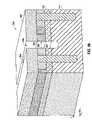
- FIG. 1illustrates a first step in a process for forming an access device and a driver.
- the processmay begin with providing a substrate 110 .
- the substrate 110may include semiconductive materials such as single-crystal or poly-crystalline silicon, gallium arsenide, indium phosphide, or other materials with semiconductor properties.
- the substrate 110may include a non-semiconductor body on which an electronic device may be constructed, e.g., a body such as a plastic or ceramic work surface.
- substrateencompasses these structures in a variety of stages of manufacture, including an unprocessed whole wafer, a partially-processed whole wafer, a fully-processed whole wafer, a portion of a diced wafer, or a portion of a diced wafer in a packaged electronic device.
- the substrate 110may include an upper doped region 112 and a lower doped region 114 .
- the depth of the upper doped region 112may be generally uniform over a substantial area of the substrate 110 , and the upper doped region 112 may be doped differently from the lower doped region 114 .
- the upper-doped region 112may include an n+ material and the lower-doped region 114 may include a p ⁇ material or vise versa.
- a pad oxide 116may be formed directly on the upper doped region 112 .
- the pad oxide 116may have a thickness less than 300 ⁇ , e.g., generally near 80 ⁇ .
- a stop body (e.g., a layer) 118may be formed on the pad oxide 116 .
- the stop body 118may include a nitride and it may have a thickness less than 300 ⁇ , e.g., generally near 95 ⁇ , but like the other structures described herein, the stop body 118 is not limited to these dimensions or materials.
- a sacrificial body 120may be formed on the stop body 118 .
- the sacrificial body 120may be made of polysilicon and it may have a thickness between 500 ⁇ and 2,000 ⁇ , e.g., generally near 1000 ⁇ .
- a lower masking body 122may be formed on the sacrificial body 120 .
- the lower masking body 122may be made of an oxide and it may have a thickness between 500 ⁇ and 2,000 ⁇ , e.g., generally near 1000 ⁇ .
- an upper masking body 124may be formed on the lower masking body 122 .
- the upper masking body 124may be made of carbon, and it may have a thickness between 1000 ⁇ and 3000 ⁇ , e.g., generally near 2000 ⁇ .
- These materials 116 , 118 , 120 , 122 and othersmay be formed with chemical-vapor deposition, spun-on coatings, or other processes know in the art.
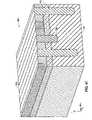
- a column mask 126may be formed, as illustrated by FIG. 3 .
- the term “column”does not refer to any particular horizontal direction on the substrate 110 other than a direction that is different from the direction that subsequently-introduced rows extend.
- the column mask 126may include a pattern of lines that define masked regions having a width 128 and exposed regions having a width 130 .
- the widths 128 and 130may be generally equal to each other and each generally equal to the lithographic-resolution limit (e.g., the photolithographic-resolution limit), referred to as “F.”
- the column mask 126may have a pitch 132 that is generally equal to 2 F.
- the lines formed by the column mask 126may be generally straight, generally parallel to each other, and may generally extend in the X-direction. These lines may be generally continuous and generally uniform in the X-direction. In other embodiments, though, the lines formed by the column mask 126 may have other shapes, e.g., they may undulate (e.g., up and down, left and right, or both), they may vary in width in the X-direction, or they may be formed from a plurality of shorter segments.
- a column hard mask 134may be formed, as illustrated by FIG. 4 .
- the column hard mask 134may be formed by generally-anisotropically etching (e.g., with a directional plasma etch) the portion of the upper masking body 124 and the portion of the lower masking body 122 that are disposed under the region not covered by the column mask 126 .
- the etchmay stop on or in the sacrificial body 120 .
- the column spacers 136may be formed on the sidewalls of the column hard mask 134 , as illustrated by FIG. 5 .
- the column spacers 136may be formed by depositing a generally conformal film (e.g., a film that is of generally uniform thickness on both vertical and horizontal structures) and, then, anisotropically etching that film to remove it from horizontal surfaces, leaving material disposed against generally vertical surfaces on the substrate 110 .
- the column spacers 136may be made of an oxide, and they may have a width 138 that is less than 100 nm, e.g., less than or generally equal to 36 nm.
- the column spacers 136may narrow the area exposed by the column hard mask 134 to a width 140 that is less than or equal to F, e.g., generally equal to or less than 3 ⁇ 4 F, 1 ⁇ 2 F, or 1 ⁇ 4 F.
- column isolation trenches 142may be formed.
- the column isolation trenches 142may be formed by generally anisotropically etching the exposed regions between the column spacers 136 .
- the column isolation trenches 142may have a width 141 that corresponds to (e.g., is generally equal to or proportional to) the width 140 .
- the column isolation trenches 142may generally extend in the X-direction and may be generally parallel to each other and generally straight.
- the cross-sectional shape of the column isolation trenches 142may be generally uniform in the X-direction.
- the column isolation trenches 142may have a depth 144 that is between 500 ⁇ and 5000 ⁇ , e.g., generally equal to 2500 ⁇ .
- the column isolation trenches 142may be filled partially or entirely with a dielectric 146 , as illustrated by FIG. 7 .
- the dielectric 146may be made of a variety of materials, such as an oxide, and it may be lined with a variety of liner films (not shown), such as an oxide liner and a nitride liner.
- the bottom of the column isolation trenches 142may be implanted or diffused with a dopant selected to further electrically isolate structures on opposing sides of the column isolation trenches 142 .
- Planarizing the substrate 110may include etching the substrate 110 or polishing the substrate with chemical-mechanical planarization. Planarization may include removing both the upper masking body 124 and the lower masking body 122 , and planarization may stop on or in the sacrificial body 120 . Additionally, an upper portion of the dielectric 146 maybe removed.
- the sacrificial body 120may be partially or entirely removed, as illustrated by FIG. 9 .
- Removing this body 120may include wet etching or dry etching the substrate 110 with an etch that selectively etches the sacrificial body 120 without removing a substantial portion of the exposed dielectric 146 , i.e., with an etch that is selective to the sacrificial body 120 .
- An etchis said to be “selective to” a material if the etch removes that material without removing a substantial amount of other types of material.
- generally vertical projections 148 formed by the dielectric 146may extend from the substrate 110 .
- a second of column spacer 150may be formed on the sidewalls of the generally vertical projections 148 of dielectric 146 , as illustrated by FIG. 10 .
- the second column spacers 150may be formed by depositing a generally conformal film on the substrate 110 and anisotropically etching the film until the film is generally removed from the horizontal surfaces, leaving the material on the vertical surfaces on the substrate 110 .
- the second column spacers 150may be made of the same material as the dielectric 146 , e.g., an oxide, or they may be made of a different material.
- the second column spacers 150may have a width 152 that is less than or generally equal to 100 nm, e.g., less than or generally equal to 36 nm.
- the spacers 150may define a width 154 between adjacent spacers 150 that is generally less than or equal to 1 F, 3 ⁇ 4 F, 1 ⁇ 2 F, or 1 ⁇ 4 F.
- the column-gate trench 152may be formed, as illustrated by FIG. 11 .
- the column-gate trench 152may be formed by generally anisotropically etching the exposed regions between the second group of column spacers 150 .
- the column-gate trenches 152may be generally parallel to each other and the column isolation trenches 142 , and they may generally extend in the X-direction.
- the column-gate trenches 152may have a depth 154 that is both less than the depth 144 ( FIG. 6 ) of the column isolation trenches 142 and greater than the depth of the upper doped region 112 .
- a column-segmenting mask 156may be formed, as illustrated by FIG. 12 .
- the column-segmenting mask 156may be a soft mask or a hard mask formed with photolithography or other patterning processes.
- the column-segmenting mask 156may define masked regions 158 and exposed regions 160 .
- the masked regions 158may extend generally in the Y-direction, and they may be generally straight and generally parallel to each other. In other embodiments, though, the masked regions 158 may undulate, vary in width, or be segmented.
- the masked regions 158may have a width generally equal to or less than F.
- the exposed regions 160may be wider than the masked regions 158 , and together, the exposed region 160 and a masked region 158 may generally define the pitch 161 of the column-segmenting mask 156 .
- the column-segmenting mask 156may be formed from photoresist or it may be a hard mask, for instance. A portion of the column-segmenting mask 156 may be disposed in the trenches 152 .
- the substrate 110may then be etched, as illustrated by FIG. 13 .
- Etching the substrate 110may include etching the substrate 110 with a generally anisotropic etch that selectively removes material from the lower doped region 114 . This may form deeper portions 162 of the column-gate trenches 152 .
- the column-segmenting mask 156may be removed, as illustrated by FIG. 14 , and the substrate 110 may be partially or substantially planarized, as illustrated by FIG. 15 .
- Planarizing the substrate 110may include selectively etching the second group of column spacers 150 and the vertical projections 148 , or this process may include planarizing these structures with chemical-mechanical planarization. In other embodiments a portion or all of the second group of column spacers 150 and the vertical projections 148 may be left on the substrate 110 and removed during subsequent steps.
- a column-gate dielectric 164may be formed, as illustrated by FIG. 16 .
- the column-gate dielectric 164may be deposited, grown, or otherwise formed, and it may substantially or entirely cover the exposed portions of the upper doped region 112 and the lower doped region 114 .
- the column-gate dielectric 164may include, consist of, or consists essentially of a variety of dielectric materials, such as oxide (e.g., silicon dioxide), oxynitride, or high-dielectric constant materials like hafnium dioxide, zirconium dioxide, and titanium dioxide, for example.
- a column gate 166may be formed, as illustrated by FIG. 17 .
- the column gate 166may be made of a conductive material, such as a metal or doped polysilicon, and it may be formed by depositing the conductive material on the substrate 110 until an overburden is formed and, then, etching the conductive material until the column gate 166 is recessed below the upper doped region 112 .
- the column gate 166is not recessed into the deeper portions 162 of the column-gate trenches 152 such that the column gate 166 is generally continuous in the X-direction between deeper portions 162 .
- a column-gate cover 168may be formed on the substrate 110 , as illustrated by FIG. 18 .
- the column-gate cover 168may be a dielectric material, such as an oxide, nitride, or other appropriate material.
- the column-gate cover 168may be formed by depositing a dielectric material on the substrate 110 and then planarizing the dielectric material with an etch or chemical-mechanical planarization.
- a row mask 170may be formed, as illustrated by FIG. 19 .
- the row mask 170may include a plurality of lines that generally extend in the Y-direction. In some embodiments, these lines are generally parallel, generally straight, and of generally uniform width in the Y-direction. In other embodiments, though, these lines may undulate, vary in width, or be segmented.
- the row mask 170may generally define masked regions 172 and exposed regions 174 , which together may repeat in the X-direction with a pitch 176 .
- the pitch 176may be generally equal to one-half of the pitch 161 ( FIG. 12 ) of the column-segmenting mask 156 .
- the mask 170may be aligned in the X-direction such that alternating exposed regions 172 of the row mask 170 overlap an edge 178 of the deeper portion 162 of the column-deep trench 152 (an arrangement that is more clearly illustrated by a post-etch view in FIG. 20 ).
- the width of the masked region 172may be generally equal to or less than F, 3 ⁇ 4 F, or 1 ⁇ 2 F.
- the row mask 170may be made of photoresist or it may be a hard mask.
- the row mask 170may be formed by double pitching a structure formed with photolithography to form sub-photo lithographic features, or other sub-photolithographic techniques may be used, such as a resist-reflow process or a resist-undercut process in which a hard mask is undercut with a wet etch.
- Double-pitchingrefers to the process of forming sidewall spacers on a patterned structure to double the number of structures defined by the patterned structure.
- the substrate 110may be etched to form fin rows 180 separated by row-gate trenches 182 , as illustrated by FIG. 20 .
- the row-gate trenches 182may be formed by generally anisotropically the etching exposed regions 174 defined by the row mask 170 .
- the row-gate trenches 182may extend into the substrate 110 to a depth that overlaps the deeper portion 162 of the column-gate trenches 152 . In some embodiments, the row-gate trenches 182 do not extend to the bottom of the deeper portion 162 , leaving a portion of the column gate 166 extending between fin rows 180 .
- a row-gate dielectric 184may be formed, as illustrated by FIG. 21 .
- the row-gate dielectric 184may be grown, deposited, or otherwise formed, and it may include one or more of the dielectric materials described above with reference to the column-gate dielectric 164 .
- row gates 186 , 187 , 188 , and 189may be formed, as illustrated by FIG. 22 .
- the row gates 186 , 187 , 188 , and 189may be formed with a sidewall-spacer process.
- a film of a conductive material, such as TiN, other appropriate metals, or doped polysilicon,may be deposited on the substrate 110 and, then, anisotropically etched to leave a conductive sidewall spacer 186 or 188 on either side of each fin row 180 .
- the row gates 186 , 187 , 188 , and 189may overlap the upper doped region 112 .
- row gates 186 and 187may be coupled to one another and at generally the same voltage, or in other embodiments, they may be controlled independently.
- row gates 188 and 189may be coupled to on another or they may be controlled independently.
- a dielectric material 190may be formed on the substrate 110 , as illustrated by FIG. 23 .
- the dielectric material 190may be an oxide, nitride, or other appropriate material, and it may isolate gates 186 , 187 , 188 , and 189 associated with adjacent fin rows 180 .
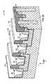
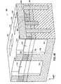
- This processmay produce an array of cells 192 each with three transistors: one transistor controlled by the row gates 188 and 189 , one transistor controlled by the column-segment gate 210 , and one transistor controlled by the row gates 186 and 187 . These transistors are described below.
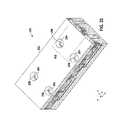
- the resulting arrayis illustrated by the perspective view of FIG. 24 , and an example of an individual cell is illustrated by FIGS. 25-30 .
- the semiconductor portion of each cell in this embodimentis illustrated by FIGS. 25 and 26 , and other aspects of an individual cell are illustrated by FIGS. 27-30 .
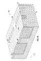
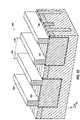
- each cell 192may include two fins 194 and 196 that are partitioned by a common cavity 198 that extends between the fins 194 and 196 .
- the fin 194may include two legs 200 and 202 that may be disposed on either side of the cavity 198
- the fin 196may include two legs 204 and 206 that may also be disposed on either side of the cavity 198 .
- the cavity 198changes depth between the legs 204 and 206 to form an elevated portion 208 that spans between the legs 204 and 206 .
- the legs 200 , 202 , 204 , and 206may include a distal portion that is formed from the upper doped region 112 and a lower portion that is formed from the lower doped region 114 .
- fin 194may form an AND gate with a pair of stacked transistors, and the fin 196 may form a single transistor.
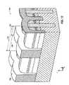
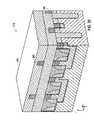
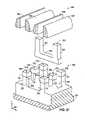
- FIG. 27is an exploded view of portions of the example of a single cell 192 .
- the cell 192may include the semiconductor portion described with reference to FIGS. 25 and 26 , a column-gate segment 210 , and the row gates 186 , 187 , 188 , and 189 .
- the column-gate segment 210may be formed from the column gate 166 by partitioning the column gate 166 during formation of the row-gate trenches 182 , as illustrated by FIG. 20 .
- the column-gate segment 210may be separated, e.g., electrically isolated, from other column-gate segments 210 formed from the same column gate 166 and other column gates 166 .
- Each column-gate segment 210may include a buried member 212 and two risers 214 and 216 .
- the risers 214 and 216may extend generally vertically and generally perpendicularly from the buried member 212 , and the buried member 212 may electrically connect the risers 214 and 216 to each other.
- the riser 216may include a lip 218 that extends generally perpendicularly from the riser 216 and is shaped to overlap the elevated portion 208 . In some embodiments, the top of the risers 214 and 216 generally do not overlap the upper doped region 212 .
- the column-gate segment 210may be generally complementary to the cavity 198 .
- the cell 192may also include the insulating members described above: the dielectric 146 , the column-gate dielectric 164 , the row-gate dielectric 184 , and the dielectric material 190 .
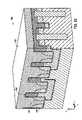
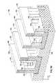
- FIGS. 28 , 29 , and 30illustrate one use for the structures described above.
- FIG. 28is a perspective view of portions the cell 192 , illustrating one way in which the cell 192 may be configured to form a data cell
- FIG. 29is a perspective view of conductive channels that may be formed during the operation of the cell 192
- FIG. 30is a circuit diagram of an example of a data cell that may be formed with the cell 192 or other cells.
- the cell 192may be connected to a data element 219 , a voltage source Vcc, a data line DL, a read control line CL READ, and a write control line CL WRITE.
- the data linemay be referred to as a digit line
- the control linesmay be referred to as word lines.
- connections to the cell 192are represented in schematic form to emphasize that the cell 192 may be connected to other devices with a variety of techniques. One example of a process for forming these connections is illustrated by subsequent figures.
- the data line DLmay connect to the legs 202 and 206 .
- the voltage sourcemay connect to the leg 200
- the data elements 219may connect to both the leg 204 and the column-gate segment 210 (viewable in FIG. 27 ).
- the data element 219may connect to the column-gate segment 210 via the riser 216 and the lip 218 .
- the read control linemay connect to or be formed from the row gates 186 and 187
- the write control linemay connect to or be formed from the row gate 189 .
- the row gate 188may be unused during some or all of the following operations of the cell 192 , or it may connect to the write control line.
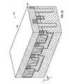
- the cell 192may form a conductive channel 220 , an example of which is illustrated by FIG. 29 .
- the channel 220may include a generally vertical portion 222 and a generally horizontal portion 224 , e.g., these portions 222 and 224 may generally form an L-shape. (Hereinafter, these portions are referred to as the vertical portion 222 and the horizontal portion 224 , which is not to suggest that these features or any others are necessarily exactly vertical, horizontal, or orthogonal).
- the vertical portion 222may include a generally nonconductive notch 226 in the upper part of the vertical portion 222 .
- the channel 220may conduct current between the leg 204 and the leg 206 .
- the distal portion of the legs 204 and 206may be referred to as a source and a drain.
- the current between the leg 204 and the leg 206is represented both by arrows 228 , corresponding to current flowing into the channel 220 from the leg 204 , and by arrows 230 , corresponding to current exiting the channel 220 through the leg 206 .
- the direction of currentmay be reversed.
- a sub-threshold voltageis a voltage that allows current to flow and may be a voltage less than the threshold voltage or a voltage greater than the threshold voltage, depending on the configuration of the cell, e.g., a PMOS-type cell or an NMOS-type cell).
- upper channel portions 232 , 234 , 236 , and 238may be established by electric fields emanating from row gates 186 and 187 .
- Each of these upper channel portions 232 , 234 , 236 , and 238may include a generally vertical portion and a generally horizontal portion, e.g., they may generally have an L-shape.
- the upper channel portions 232 and 234may be formed in the leg 200
- the upper channel portions 236 and 238may be formed in the leg 202 .
- the upper channel portions 232 and 234may be connected to the upper channel portions 236 and 238 by a lower channel 240 .
- the lower channel 240may be generally orthogonal to both the generally horizontal and the generally vertical portions of the upper channel portions 232 , 234 , 236 , and 238 .
- the lower channel 240generally extends in the X-direction and generally has a U-shaped cross section.
- the lower channel 240may be formed by electric fields emanating from the column-gate segment 210 ( FIG. 27 ).
- the fin 194may form an AND gate with a pair of upper transistors that are controlled by the row gates 186 and 187 and a lower transistor that is controlled by the column-gate segment 210 .
- An example of current flowis illustrated by arrows 242 and 244 , depicting current flow into the upper channel portions 232 and 234 .
- These currents 242 and 244may flow through the lower channel 240 and, then, out the upper channel portions 236 and 238 , as illustrated by arrows 246 and 248 .
- the upper channel portions 232 and 234may be said to be connected in series to the upper channel portions 236 and 238 by the lower channel 240 . In other embodiments or other operations, the direction of current may be reversed.
- FIG. 30illustrates the cell 192 (and other cells in accordance with the present technique) in circuit schematic form.
- the illustrated cell 192may include the data element 219 , a transistor 250 , and a driver 252 .
- the data element 219may include a variety of different types of data elements.
- the data element 219may include a sensor, such as an image sensor, e.g., a charge-coupled device or photodiode, or a memory element.
- volatile memory elementssuch as dynamic random access memory (DRAM)
- nonvolatile memory elementssuch as phase-change memory elements (e.g., ovonic devices), floating gate memory elements, ferroelectric memory elements, magnetoresistive memory elements, and semiconductor-oxide-nitride-oxide-semiconductor (SONOS) memory elements.
- DRAMdynamic random access memory
- nonvolatile memory elementssuch as phase-change memory elements (e.g., ovonic devices), floating gate memory elements, ferroelectric memory elements, magnetoresistive memory elements, and semiconductor-oxide-nitride-oxide-semiconductor (SONOS) memory elements.
- phase-change memory elementse.g., ovonic devices
- floating gate memory elementse.g., ferroelectric memory elements
- magnetoresistive memory elementse.g., magnetoresistive memory elements
- SONOSsemiconductor-oxide-nitride-oxide-semiconductor
- the transistor 250 illustrated by FIG. 30may be formed by the fin 196 of FIG. 28
- the driver 252 illustrated by FIG. 30may be formed by the fin 194 of FIG. 28
- the driver 252may include two access transistors 254 and 256 and an amplifying transistor 258 .
- the access transistors 254 and 256may be formed by legs 200 and 202 of the fin 194 , as illustrated by FIG. 28
- the amplifying transistor 258may be formed by the portion of the fin 194 adjacent the column-gate segment 210 , as illustrated by FIG. 27 .
- the access transistors 254 and 256may be referred to as read-access devices, and the transistor 250 may be referred to as a write-access device.
- Other embodimentsmay include other types of read-access and write-access devices, such as diodes.
- the cell 192 illustrated by FIG. 30may output data from the data element 219 .
- the data element 219may apply a voltage to the gate of the amplifying transistor 258 , and the amplifying transistor 258 may amplify this signal.
- the amplifying transistor 258may be configured to operate in its triode region, and it may drive a current between its source and its drain that varies according to the voltage from the data element 219 , e.g., the amplifying transistor 258 may conduct a current that is generally proportional to the voltage of its gate.
- the access transistors 254 and 256may close a path between the voltage source Vcc and the data line DL.
- the access transistors 254 and 256may enter a conductive state, allowing current to flow between the data line DL and the voltage source Vcc, through the amplifying transistor 258 .
- the magnitude of the current to or from the data line DLmay be controlled, in part or substantially entirely, by a voltage that the data element 219 applies to the gate of the amplifying transistor 258 .
- current flowing between the data line DL and the voltage source Vccmay be indicative of (e.g., generally proportional to) a data value being output from the data element 219 .
- driver 252Some embodiments of the driver 252 are believed to increase the speed and accuracy with which the data element 219 conveys data through the data line DL. Because the current flowing into the data line DL is supplied by the voltage source Vcc rather than the data element 219 , the speed with which the data line DL changes voltage when reading data may be at least partially decoupled from the size of the data element or its signal. Thus, relatively small data elements 219 that supply relatively small currents may still rapidly change the digit line DL voltage.
- the data element 219may convey multiple bits, e.g., 2, 3, 4, 5 or more bits of data, through relatively small changes in the voltage applied to the gate of the amplifying transistor 258 . These relatively small differences in voltage may be amplified by the driver 252 and output via the data line DL. Thus, the resolution of the data element 219 may be increased by amplifying signals with the driver 252 .
- datamay be written to the data element 219 .
- a signalmay be asserted on the write control line CL WRITE, and this signal may turn on the transistor 250 .
- the transistor 250When the transistor 250 is turned on, current may flow from the data line DL to the data element 219 , and this current may change a property of the data element 219 , e.g., a stored charge or degree of crystallintity.
- the change in the property of the data element 219may be used to store data.
- FIGS. 31-38illustrate an example of a process for connecting the cell 192 of FIG. 28 to a capacitor memory element.
- digit lines 260may be formed on the substrate 110 .
- the digit lines 260may generally extend in the X-direction, and they may connect to the legs 206 and 202 of the cells 192 .
- the data lines 260may be generally straight, but in other embodiments they may have other shapes, e.g., they may undulate, vary in width, or be segmented.
- the data lines 260may be spaced above the legs 202 and 206 , and they may be connected to the legs 202 and 206 through a via, a contact, or other structure.
- a dielectric body 262may be formed on the data lines 260 , as illustrated by FIG. 32 , and vias 264 may be opened through the dielectric body 262 , as illustrated by FIG. 33 .
- the vias 264may expose the legs 200 in each of the cells 192 .
- the vias 264may be formed by patterning the substrate 110 with photolithography and then generally anisotropically etching the substrate 110 to remove exposed portions of the dielectric body 262 .
- contacts 266may be formed in the vias 264 and voltage-source connectors 268 may be formed, as illustrated by FIG. 34 .
- the contacts 266may be formed by depositing a generally conductive material, such as one or more of the conductive materials described above, on the substrate 110 and etching the conductive material until the conductive material remains primarily inside the vias 264 .
- the power-source connectors 268may be formed by depositing a generally conductive film and patterning and etching the conductive film.
- the illustrated voltage-source connectors 268extend generally in the Y-direction. In other embodiments, they may extend in other directions, e.g., the X-direction, or they may be formed from a conductive plate.
- the dielectric body 270may be made of an oxide, a nitride, a spun-on dielectric, or other appropriate materials.
- vias 272may be formed through the dielectric body 270 and the dielectric body 262 , as illustrated by FIG. 36 .
- the vias 272may be formed by patterning the substrate 110 with photolithography and generally anisotropically etching the substrate 110 .
- the vias 272may overlap both the leg 204 and the riser 216 of the column-gate segment 210 .
- the etch that opens the vias 272may selectively remove a portion of the column-gate cover 168 to expose part of the column-gate segments 210 . In certain embodiments, this etch may not remove a substantial portion of the protective dielectric 190 that covers the row gates 186 , 187 , 188 , and 190 , such that these structures remained generally isolated from the column-gate segment 210 .
- capacitor plates 274may be formed on the substrate 110 , as illustrated by FIG. 37 .
- the capacitor plates 274may include an upper, cup-shaped portion 276 and a lower contact 278 .
- the cup-shaped portion 276may be formed by depositing a sacrificial layer and, then, etching holes that are complementary to the capacitor plates 274 in the sacrificial layer. After forming the holes, a generally conformal film may be deposited on the sacrificial layer and planarized, e.g., with chemical-mechanical planarization, to remove the portion of the conformal film disposed outside of the holes, thereby leaving the cup-shaped portion 276 .
- the capacitor plates 274may be made of a conductive material, e.g., a metal, doped polysilicon, or other appropriate materials.
- the lower contact 278may connect to both the leg 204 and the riser 216 of the column-gate segment 210 .
- a capacitor dielectricmay be deposited on the capacitor plates 274 , and a common capacitor plate may be formed by depositing a conductive film on the substrate 110 , thereby forming capacitors.
- the capacitor plates 274may store data by accumulating a charge.
- the size of the chargemay correspond to particular data values, e.g., a small charge may correspond to a zero and a larger charge may correspond to a one.
- the range of stored chargemay be divided into smaller increments corresponding to multiple bit data values, e.g., two, three, four, or more bits.
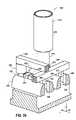
- FIG. 38illustrates an example of a single cell 192 connected to the capacitor plate 274 .
- the capacitor plate 274is the data element
- the fin 196forms an access device controlled by the row gate 189
- the fin 194forms a driver controlled by both the row gates 186 and 187 and the column-gate segment 210 ( FIG. 27 ).
- currentmay flow from the voltage-source connector 268 to the data line 260 depending on the magnitude of the voltage asserted by the capacitor plate 274 on the column-gate segment 210 ( FIG. 27 ).
- the magnitude of this current from the voltage sourcemay indicate the value of data stored by the capacitor plate 274 by changing the voltage of the data line 260 .
- a rise in the voltage of the digit line 260may correspond to a stored data value of 1
- a decrease in the voltage of the digit line 260may correspond to a stored data value of 0.
- FIG. 39illustrates one example of an array 280 of the cells 192 .
- the illustrated array 280may include a plurality of cells 192 , a read-control driver 282 , a write-control driver 284 , a data sensor 286 , a data driver 288 , and a voltage source 290 .
- the cells 192may each include a capacitor plate 274 , the column-gate segment 210 , and the legs 200 , 202 , 204 , and 206 .
- the legs 202 and 206 of the cells 192may connect to the data driver 288 and the data sensor 286 , and the leg 200 may connect to the voltage source 290 via the voltage-source connector 268 .
- the data driver 288may output a voltage or current through the data lines 260 to write data to the capacitor plates 274 , and the data sensor 286 may read, e.g. categorize into discrete categories corresponding to digital values, currents or voltages output by the cells 192 on the data lines 260 .
- the read-control driver 282may be configured to select cells 192 for reading by asserting a voltage on the row gates 186 and 187 of a selected cell 192 . In some embodiments, these row gates 186 and 187 may be referred to as read control lines or read word lines.
- the write-control driver 284may be configured to select a cell 192 by asserting a voltage on the row gate 189 associated with that cell 192 .
- the row gates 189may be referred to in some embodiments as write-control lines or write word lines.
- the illustrated cells 192 in the array 280may be arranged in a generally rectangular lattice (e.g., they may have generally similar orientations and may be arranged in generally orthogonal rows and columns). In other embodiments, they may have other arrangements.
- the cells 192may be arranged in offsetting rows in a hexagonal lattice, or the cells 192 may be arranged with different orientations in adjacent rows, as illustrated by an array 292 of FIG. 40 .
- the cells 192may be oriented in a first direction, and the cells 192 ′ in adjacent rows may be oriented in an opposite direction and offset by approximately one-half of a cell 192 .
- FIGS. 41-63illustrate another example of a process for forming a data cell with a driver.
- the processbegins with obtaining a substrate 294 in the state illustrated by FIG. 41 .
- the substrate 294may be obtained by executing (or contracting with others to execute) the steps illustrated by FIGS. 1-10 and described above.
- the substrate 294may include the previously-described upper doped region 112 , lower doped region 114 , column isolation trenches 142 , dielectric 146 , vertical projections 148 , and second group of column spacers 150 .
- the substrate 294 of FIG. 41may be different from the substrate 110 of FIG. 10 in at least one regard.
- the gaps 295 between adjacent column spacers 150may be wider than the gaps 154 ( FIG. 10 ).
- the wider gaps 295may be made wider by adjusting the spacing of the column mask 126 ( FIG. 3 ) to increase the distance between pairs of the column isolation trenches 142 .
- a third column spacer 296may be formed, as illustrated by FIG. 42 .
- the third column spacer 296may be formed by depositing a film on the substrate 294 and then generally anisotropically etching that film to remove the film from horizontal surfaces.
- the third column spacer 296may generally define a gap 298 in the wider gap 295 .
- the gap 298may be generally equal to the gap 154 ( FIG. 3 ).
- the third column spacer 296may be made of a different material from the second group of column spacers 150 and the vertical projections 148 to facilitate selective removal of the third column spacer 296 .
- the second group of column spacers 150 and the vertical projections 148may be an oxide and the third column spacer 296 may be polysilicon.
- a masking material 300may be formed on the substrate 294 , as illustrated by FIG. 43 .
- the masking material 300may be formed with an overburden 302 to planarize the substrate 294 .
- the masking material 300is a different material from the third column spacer 296 to facilitate selective removal of these materials.
- the masking material 300may be an oxide.
- Planarizingmay include etching the substrate 294 with an etch that is generally nonselective among the materials being etched (such as an etch referred to in the art as an “alligator etch”) or polishing the substrate 294 with chemical-mechanical planarization.
- a column-notch mask 302may be formed, as illustrated by FIG. 45 .
- the column-notch mask 302may be a hard mask (e.g., an oxide hard mask), or it may be made of photoresist.
- the column-notch mask 302may generally cover the substrate 294 with the exception of the space above one of the third column spacers 296 between pairs of the column isolation trenches 142 .
- an exposed region 304 of the column-notch mask 302may be generally aligned with the left third column spacer 296 .
- the exposed region 304may be made wider than the left third column spacer 296 to increase the alignment margin in the Y-direction, as the structures 150 and 300 adjacent the left third column spacer 296 may function as a hard mask.
- a column notch 306may be formed in the substrate 294 , as illustrated by FIG. 46 .
- the column notch 306may be formed by selectively etching the third column spacer 296 disposed under the exposed region 304 and, then, using the second group of column spacers 150 and the masking material 300 as a mask to etch through the upper doped region 112 .
- the third column spacer 296may be removed with a tetramethylammonium hydroxide (TMAH) etch. Removing one of the third column spacers 296 may form a gap 308 that may generally define the width of the column notch 306 .
- the gap 308may be narrower than or generally equal to 1 F, 3 ⁇ 4 F, or 1 ⁇ 2 F.
- the column-notch mask 302may be removed and the column notch 306 may be partially or entirely filled with a column-notch dielectric 310 , as illustrated by FIG. 47 .
- the column-notch dielectric 310may be formed by depositing a dielectric material, such as an oxide like tetra-ethyl-ortho-silicate (TEOS), in the column notch 306 until the column notch 306 is substantially filled.
- TEOStetra-ethyl-ortho-silicate
- the column-notch dielectric 310may include one or more liner materials, such as an oxide and a nitride liner, adjacent the upper doped region 112 and the lower doped region 114 .
- a second column-notch mask 312may be formed on the substrate 294 , as illustrated by FIG. 48 .
- the second column-notch mask 312may be a hard mask (e.g., an oxide hard mask) or it may be made of photoresist, and it may define a plurality of exposed regions 314 .
- the exposed regions 314may be arranged in a generally rectangular lattice, but in other embodiments, they may be arranged differently, e.g., in a generally hexagonal lattice.
- the illustrated exposed regions 314may define a generally cuboid volume, but in other embodiments, they may have other shapes, e.g., they may generally define a right-elliptical-cylindrical volume or a right-circular-cylindrical volume. In this embodiment, the exposed regions 314 are generally disposed over the remaining third column spacer 296 and are generally aligned with this structure. To increase alignment margins in the Y-direction, the exposed regions 314 may have a width 316 that is wider than a width 318 of the remaining third column spacer 296 .
- column-trench segments 319may be formed in the substrate 294 .
- the column-trench segments 319may be formed in two steps.
- a portion of the third column spacer 296 disposed under the exposed regions 314may be removed, for example, with a TMAH wet etch or a dry etch. This portion of the third column spacer 296 may be removed with an etch that is generally selective to the third column spacer 296 and not to either the second column spacer 150 or the masking material 300 .
- a substantial portion of these materials 150 and 300may remain on the substrate 294 , thereby functioning as a hard mask that defines a width 320 that is narrower than the width 316 of the exposed regions 314 .
- the remainder of the column-trench segments 319may be formed.
- the upper dopped region 112 and the lower doped region 114may be generally anisotropically etched, using the second column-notch mask 312 to define features in the X-direction and both the second group of column spacers 150 and the masking material 300 to define features in the Y-direction.
- the column-trench segments 319may have a width that is generally equal to the width 308 of the column notch 306 .
- the bottom of one or both sides of the column-trench segment 319may be implanted with a high Vth implant to suppress N-channel formation of parasitic devices.
- the right side 321 of the column-trench segment 319may be implanted with an angled implant.
- the second column-notch mask 312may be removed, and a column-gate dielectric 322 may be formed, as illustrated by FIG. 50 .
- the column-gate dielectric 322may include any of the materials described above with reference to the column-gate dielectric 164 illustrated by FIG. 21 .
- column-gate segments 324may be formed, as illustrated by FIG. 51 .
- the column-gate segments 324may be formed by depositing, e.g., with chemical-vapor deposition or physical-vapor deposition, a conductive material, such as a metal or doped polysilicon (e.g., an n+ doped polysilicon), on the substrate 294 .
- the conductive materialmay then be etched to recess the conductive material into the column-trench segments 319 .
- the column-gate segments 324may generally extend in the X-direction and may be generally isolated from other column-gate segments 324 at this stage of the process.
- the substrate 294may be planarized, as illustrated by FIG. 52 .
- Planarizingmay include removing some or substantially all of the materials disposed above the upper doped region 112 .
- the substrate 294may be planarized with chemical-mechanical planarization or a generally non-selective etch, such as an alligator etch.
- a row mask 326may be formed on the substrate 294 , as illustrated by FIG. 53 .
- the row mask 326may be a soft mask or a hard mask, and it may generally define a plurality of masked regions 328 and exposed regions 330 , both of which may generally extend in the Y-direction.
- the width of the masked regions 328may be defined with sub-photolithographic techniques, such as double pitching or reflowing a mask formed with the photolithography.
- the masked regions 328may be generally parallel to each other and generally straight, or in other embodiments, they may have other shapes, e.g., they may undulate side to side, they may be discontinuous, or they may vary in width along the Y-axis. In some embodiments, the width of the masked region 328 is generally equal to or less than F, 3 ⁇ 4 F, or 1 ⁇ 2 F. The width 330 may be larger than the width 328 , e.g., in some embodiments, the width 330 may be generally equal to F.
- the masked regions 328may be generally aligned with, and partially or substantially entirely disposed over, opposite ends of the column-gate segments 324 .
- row-gate trenches 332may be formed, as illustrated by FIG. 54 .
- the row-gate trenches 332may be formed by generally anisotropically etching the substrate 294 between the masked regions 328 .
- the row-gate trenches 332may define fin rows 334 .
- the row-gate trenches 332may have a depth 336 that is greater than a depth 338 of the column notch 306 , but in some embodiments, not as large as a depth 340 of the column-trench segments 319 .
- the row mask 326may be removed, and a row-gate dielectric 342 may be formed on the substrate 294 , as illustrated by FIG. 55 .
- the row-gate dielectric 341may include any of the materials described above with reference to the column-gate dielectric 164 in FIG. 21 .
- row gates 342 , 344 , 346 , and 348may be formed, as illustrated by FIG. 56 .
- the row gates 342 , 344 , 346 , and 348may be formed with a sidewall-spacer process, e.g., by depositing a blanket film of a conductive material and, then, generally anisotropically etching the conductive material to remove the conductive material from horizontal surfaces, while leaving some conductive material adjacent generally vertical surfaces.
- the row gates 342 , 344 , 346 , and 348may be made of or include a variety of conductive materials, such as metals (e.g., TiN) or doped polysilicon.
- the illustrated row gates 342 , 344 , 346 , and 348generally extend in the X-direction and may be generally perpendicular to the column-gate segments 324 .
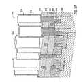
- FIG. 56illustrates an array of cells 350 , and portions of an individual cell 350 are illustrated in greater detail by FIG. 57 .
- FIG. 57illustrates an exploded view of the row gates 342 , 344 , 346 , and 348 , the column-gate segment 324 , and a semiconductive portion 358 of the cell 350 , which may be formed by the upper doped region 112 and the lower doped region 114 .
- the insulating portions of the cell 350are not shown in FIG. 57 .
- the cells 350may consume a horizontal surface area of generally equal to or less than 30 F 2 , 25 F 2 , or 18 F 2 .
- the column-gate segment 324may be generally symmetric and may include risers 352 and 354 joined by a buried member 356 .
- the risers 352 and 354may be disposed at or near opposite distal portions of the buried member 356 .
- the risers 352 and 354may be generally perpendicular to the buried member 356 , which may extend generally horizontally in the X-direction.
- the column-gate segment 324may be characterized as generally having a U-shape.
- the column-gate segment 324may be generally electrically isolated from other column-gate segments in other cells 350 , with the exception of subsequently-formed connections. Further, in some embodiments, the column-gate segment 324 may also be generally electrically isolated from the row gates 342 , 344 , 346 , and 348 , again with the exception of some subsequently-formed connections.
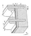
- the semiconductive portion 350may include two fins 360 and 362 and a cavity 364 .
- Each of the fins 360 and 362may include three legs 366 , 368 , 370 , 372 , 374 , and 376 .
- the fins 360 and 362may include more or fewer legs within a single cell 350 .
- the legs 366 and 368 and the legs 372 and 374may be separated from one another by notches 378 and 380 . These notches 378 and 380 may be deeper than the upper doped region 112 , but in some embodiments, not as deep as a height 382 of the fins 360 and 362 .
- the other legs 368 and 370 and 374 and 376may be separated from one another by the cavity 364 , which may extend beyond the height 382 of the fins 360 and 362 .
- the shape of the cavity 364may be generally complementary to the shape of the column-gate segment 324 .
- FIGS. 58-63illustrate one way in which the cell 350 may be connected to a data element, such as the capacitor plate 274 .
- the cell 350may be connected to the capacitor plate 274 , the digit lines 260 , and the voltage-source connector 268 with a modified version the process described above with reference to FIGS. 31-38 .
- the positions of the contact 266 and the lower contact 278may be shifted relative to the data line 260 to align the contacts 266 and 278 with certain portions of the cell 350 .
- the data line 260may be connected to the legs 366 and 372 , and the contact 266 may connect the voltage-source connector 268 to the leg 370 .
- the lower contact 278may connect the cup-shaped portion 276 of the capacitor plate 274 to both the legs 374 and 376 and the riser 354 of the column-gate segment 324 .
- the cell 350may also include the dielectric bodies 262 and 270 and other insulators illustrated by FIG. 37 .
- the cell 350may behave similar or identically to the circuit illustrated by FIG. 30 .
- the row gates 342 and 344may function as read control lines CL READ, and the row gates 346 and 348 may function as a write control lines CL WRITE.
- the fin 360may function as the driver 252 , and the fin 362 may function as the transistor 250 .
- FIGS. 61-63illustrate current through the cell 350 .
- the row gates 346 and 348may be energized, and the capacitor plate 274 may be charged or discharged, as illustrated by FIG. 61 .
- the charge of the capacitor plate 274may be adjusted by a current between the capacitor plate 274 and the data line 260 , as indicated by the arrow 360 .
- the current 360may flow from the upper doped portion 112 of the leg 372 , through a channel in the lower doped portion 114 , to the upper doped portion 112 of the leg 374 .
- the channel in the lower doped portion 114may be formed by electric fields emanating from the row gates 346 and 348 ( FIG. 58 ).
- the cell 350may form two, generally parallel channels each adjacent one of the row gates 346 and 348 on either side of the fin 362 .
- These channelsmay generally have a U-shape, as indicated by the arrow 360 in FIG. 61 , and they may form a conductive path around the column-notch dielectric 310 , joining the upper doped regions 112 of the legs 372 and 374 .
- the current 360may flow towards or away from the capacitor plate 274 , depending on the embodiment, the data value being written to the capacitor plate 274 , and the data value formerly written to the capacitor plate 274 . In some embodiments, a portion of this current 360 may also charge, or discharge, the column-gate segment 324 . Once the charge of the capacitor 274 is adjusted to reflect the data value being written, the row gates 346 and 340 at may be de-energized, closing the conductive channel between the legs 372 and 374 and impeding the charge on the capacitor plate 274 from changing.
- a current between the voltage-source connector 268 and the data line 260may be categorized as corresponding to a data value, e.g., 0, 1, or a multi-bit digital value.
- the magnitude of this currentmay be affected by data stored by the capacitor plate 274 .
- the voltage of the capacitor plate 274may correspond to (e.g., be generally the same as) the voltage of the column-gate segment 324 , as this voltage may propagate through the lower contact portion 278 of the capacitor plate 274 , through the riser 354 of the column-gate segment 324 , across the buried member 356 , and into the riser 352 . This path is illustrated by the cross-sectional view of FIG. 63 .
- An electric field emanating from the column-gate segment 324 , and more specifically, the riser 352 ,may establish a conductive channel that extends between the upper doped region 112 of the leg 372 and the upper doped region 112 of the leg 368 . As illustrated by FIG. 62 , this conductive channel may carry a current between the voltage-source connector 268 and the leg 368 , as indicated by arrow 362 .
- the row gates 342 and 344When reading data, the row gates 342 and 344 may be energized, and electric fields from the use or row gates 342 and 344 may establish a channel that carries a current between the leg 368 and the leg 366 , as illustrated by arrow 364 .
- energizing the row gates 342 and 344may establish two conductive channels on either side of the fin 360 , and these conductive channels may connect the upper doped regions 112 of the legs 366 and 368 by extending around the column-notch dielectric 310 .
- the channels from the row gates 342 and 344 and the channel from the column-gate segment 324may both generally have a U-shape, and the channels from the row gates 342 and 344 may be generally orthogonal to the channel from the column-gate segment 324 .
- currentmay flow between the voltage-source connector 268 and the data line 260 depending, in part, on the charge of the capacitor plate 274 . If the capacitor plate 274 is charged, the column-gate segment 324 may also be charged, and an electric field from the column-gate segment 324 may form a conductive channel for the current 362 . If the capacitor plate 274 is not charged, then, in some embodiments, the column-gate segment 324 may not establish a conductive channel between the legs 368 and 370 , and current may not flow between the voltage-source connector 268 and the data line 260 . Current flow during a read operation may also depend, in part, on the transistors formed by the legs 368 and 370 , as they may establish the part of the conductive path between the voltage-source connector 268 and the data line 260 that carries the current 364 .
- FIGS. 58-63may be one example of the circuit illustrated by FIG. 30 .
- the column-gate segment 324may drive the current 362 ( FIG. 62 ) based on the voltage of the capacitor plate 274 , functioning as the amplifying transistor 258 in the driver 215 illustrated by FIG. 30 .
- transistors formed by the legs 366 and 368 and the row gates 342 and 344may function as the access transistors 254 and 256 in the driver 252 illustrated by FIG. 30 . Together, they may form an AND gate.
- the readis non-destructive, e.g., the charge and corresponding data remains on the capacitor even after reading.
- some embodimentsmay operate at a speed similar to SRAM.
- the added signal strengthmay also be used to lengthen the digit lines, which may reduce the number of sense amplifiers on a chip and reduce die size.
- multiple bitsmay be stored on a single memory element, and the driver may amplify smaller differences in signals corresponding to the different data values. Not all embodiments will provide all of these benefits, and some embodiments may be useful for other reasons and may provide none of these benefits.
Landscapes
- Engineering & Computer Science (AREA)
- Manufacturing & Machinery (AREA)
- Microelectronics & Electronic Packaging (AREA)
- Computer Hardware Design (AREA)
- Semiconductor Memories (AREA)
- Metal-Oxide And Bipolar Metal-Oxide Semiconductor Integrated Circuits (AREA)
- Thin Film Transistor (AREA)
Abstract
Description
- 1. Field of Invention
- Embodiments of the invention relate generally to electronic devices and, more specifically, in certain embodiments, to electronic devices having data cells with drivers.
- 2. Description of Related Art
- Many types of electronic devices have a plurality of data cells. Typically, the data cells each include a data element (e.g., a memory element, an imaging element, or other device configured to output data, such as various kinds of sensors) and, in some instances, an access device, such as a transistor or diode. Generally, the access device controls access to the data element, and the data element outputs signals indicative of stored or sensed data.
- In some electronic devices, the signals from the data elements are too weak to be reliably sensed. Typically, the data elements are made relatively small to increase the functionality of electronic devices and lower their cost. One consequence of this practice, though, is that some data elements output signals that are relatively weak, e.g., of low intensity. As a result, it can be difficult to use the signals for useful purposes, such as indicating a digital value (e.g., 0, 1, 00, 01, etc.) or an analog value that is stored or sensed by a data element.
FIGS. 1-29 illustrate steps in a process for forming an access device and a driver in accordance with an embodiment of the present technique;FIG. 30 illustrates a circuit schematic of a single data cell that may be formed with the access device and the driver illustrated byFIGS. 1-29 .FIGS. 30-38 illustrate a process for forming a data element connected to the access device and the driver ofFIGS. 1-30 ;FIGS. 39 and 40 illustrate two embodiments of arrays of data cells in accordance with an embodiment of the present technique;FIGS. 41-57 illustrate steps in a second embodiment of a process for forming an access device and a driver in accordance with an embodiment of the present technique; andFIGS. 58-63 illustrate a data cell formed with the access device and the driver produced by the process ofFIGS. 41-57 .FIG. 1 illustrates a first step in a process for forming an access device and a driver. The process may begin with providing asubstrate 110. Thesubstrate 110 may include semiconductive materials such as single-crystal or poly-crystalline silicon, gallium arsenide, indium phosphide, or other materials with semiconductor properties. Alternately, or additionally, thesubstrate 110 may include a non-semiconductor body on which an electronic device may be constructed, e.g., a body such as a plastic or ceramic work surface. The term “substrate” encompasses these structures in a variety of stages of manufacture, including an unprocessed whole wafer, a partially-processed whole wafer, a fully-processed whole wafer, a portion of a diced wafer, or a portion of a diced wafer in a packaged electronic device.- The
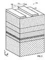
substrate 110 may include an upperdoped region 112 and a lowerdoped region 114. The depth of the upperdoped region 112 may be generally uniform over a substantial area of thesubstrate 110, and the upperdoped region 112 may be doped differently from the lowerdoped region 114. For example, the upper-dopedregion 112 may include an n+ material and the lower-dopedregion 114 may include a p− material or vise versa. - Next, several films may be formed on the
substrate 110, as illustrated byFIG. 2 . Apad oxide 116 may be formed directly on the upperdoped region 112. Thepad oxide 116 may have a thickness less than 300 Å, e.g., generally near 80 Å. A stop body (e.g., a layer)118 may be formed on thepad oxide 116. Thestop body 118 may include a nitride and it may have a thickness less than 300 Å, e.g., generally near 95 Å, but like the other structures described herein, thestop body 118 is not limited to these dimensions or materials. Asacrificial body 120 may be formed on thestop body 118. Thesacrificial body 120 may be made of polysilicon and it may have a thickness between 500 Å and 2,000 Å, e.g., generally near 1000 Å. Alower masking body 122 may be formed on thesacrificial body 120. Thelower masking body 122 may be made of an oxide and it may have a thickness between 500 Å and 2,000 Å, e.g., generally near 1000 Å. Finally, anupper masking body 124 may be formed on thelower masking body 122. Theupper masking body 124 may be made of carbon, and it may have a thickness between 1000 Å and 3000 Å, e.g., generally near 2000 Å. Thesematerials - Next, a
column mask 126 may be formed, as illustrated byFIG. 3 . (The term “column” does not refer to any particular horizontal direction on thesubstrate 110 other than a direction that is different from the direction that subsequently-introduced rows extend.) Thecolumn mask 126 may include a pattern of lines that define masked regions having awidth 128 and exposed regions having awidth 130. Thewidths column mask 126 may have apitch 132 that is generally equal to 2 F. The lines formed by thecolumn mask 126 may be generally straight, generally parallel to each other, and may generally extend in the X-direction. These lines may be generally continuous and generally uniform in the X-direction. In other embodiments, though, the lines formed by thecolumn mask 126 may have other shapes, e.g., they may undulate (e.g., up and down, left and right, or both), they may vary in width in the X-direction, or they may be formed from a plurality of shorter segments. - After forming the
column mask 126, a columnhard mask 134 may be formed, as illustrated byFIG. 4 . The columnhard mask 134 may be formed by generally-anisotropically etching (e.g., with a directional plasma etch) the portion of theupper masking body 124 and the portion of thelower masking body 122 that are disposed under the region not covered by thecolumn mask 126. In some embodiments, the etch may stop on or in thesacrificial body 120. - Next, the
column mask 126 may be removed, and thecolumn spacers 136 may be formed on the sidewalls of the columnhard mask 134, as illustrated byFIG. 5 . Thecolumn spacers 136 may be formed by depositing a generally conformal film (e.g., a film that is of generally uniform thickness on both vertical and horizontal structures) and, then, anisotropically etching that film to remove it from horizontal surfaces, leaving material disposed against generally vertical surfaces on thesubstrate 110. Thecolumn spacers 136 may be made of an oxide, and they may have awidth 138 that is less than 100 nm, e.g., less than or generally equal to 36 nm. Thecolumn spacers 136 may narrow the area exposed by the columnhard mask 134 to awidth 140 that is less than or equal to F, e.g., generally equal to or less than ¾ F, ½ F, or ¼ F. - Next, as illustrated by
FIG. 6 ,column isolation trenches 142 may be formed. Thecolumn isolation trenches 142 may be formed by generally anisotropically etching the exposed regions between thecolumn spacers 136. Thecolumn isolation trenches 142 may have awidth 141 that corresponds to (e.g., is generally equal to or proportional to) thewidth 140. Thecolumn isolation trenches 142 may generally extend in the X-direction and may be generally parallel to each other and generally straight. The cross-sectional shape of thecolumn isolation trenches 142 may be generally uniform in the X-direction. In some embodiments, thecolumn isolation trenches 142 may have adepth 144 that is between 500 Å and 5000 Å, e.g., generally equal to 2500 Å. - After forming the
column isolation trenches 142, they may be filled partially or entirely with a dielectric146, as illustrated byFIG. 7 . The dielectric146 may be made of a variety of materials, such as an oxide, and it may be lined with a variety of liner films (not shown), such as an oxide liner and a nitride liner. In some embodiments, prior to forming the dielectric146, the bottom of thecolumn isolation trenches 142 may be implanted or diffused with a dopant selected to further electrically isolate structures on opposing sides of thecolumn isolation trenches 142. - Next, the
substrate 110 may be planarized, as illustrated byFIG. 8 . Planarizing thesubstrate 110 may include etching thesubstrate 110 or polishing the substrate with chemical-mechanical planarization. Planarization may include removing both theupper masking body 124 and thelower masking body 122, and planarization may stop on or in thesacrificial body 120. Additionally, an upper portion of the dielectric146 maybe removed. - Next, the
sacrificial body 120 may be partially or entirely removed, as illustrated byFIG. 9 . Removing thisbody 120 may include wet etching or dry etching thesubstrate 110 with an etch that selectively etches thesacrificial body 120 without removing a substantial portion of the exposeddielectric 146, i.e., with an etch that is selective to thesacrificial body 120. An etch is said to be “selective to” a material if the etch removes that material without removing a substantial amount of other types of material. After removing thesacrificial body 120, generallyvertical projections 148 formed by the dielectric146 may extend from thesubstrate 110. - Next, a second of
column spacer 150 may be formed on the sidewalls of the generallyvertical projections 148 ofdielectric 146, as illustrated byFIG. 10 . As with the previously-describedcolumn spacers 136, thesecond column spacers 150 may be formed by depositing a generally conformal film on thesubstrate 110 and anisotropically etching the film until the film is generally removed from the horizontal surfaces, leaving the material on the vertical surfaces on thesubstrate 110. Thesecond column spacers 150 may be made of the same material as the dielectric146, e.g., an oxide, or they may be made of a different material. Thesecond column spacers 150 may have awidth 152 that is less than or generally equal to 100 nm, e.g., less than or generally equal to 36 nm. Thespacers 150 may define awidth 154 betweenadjacent spacers 150 that is generally less than or equal to 1 F, ¾ F, ½ F, or ¼ F. - After forming the second group of
column spaces 150, thecolumn-gate trench 152 may be formed, as illustrated byFIG. 11 . Thecolumn-gate trench 152 may be formed by generally anisotropically etching the exposed regions between the second group ofcolumn spacers 150. Thecolumn-gate trenches 152 may be generally parallel to each other and thecolumn isolation trenches 142, and they may generally extend in the X-direction. Thecolumn-gate trenches 152 may have adepth 154 that is both less than the depth144 (FIG. 6 ) of thecolumn isolation trenches 142 and greater than the depth of the upperdoped region 112. - Next, a column-segmenting
mask 156 may be formed, as illustrated byFIG. 12 . The column-segmentingmask 156, like the other masks discussed, may be a soft mask or a hard mask formed with photolithography or other patterning processes. The column-segmentingmask 156 may definemasked regions 158 and exposedregions 160. Themasked regions 158 may extend generally in the Y-direction, and they may be generally straight and generally parallel to each other. In other embodiments, though, themasked regions 158 may undulate, vary in width, or be segmented. Themasked regions 158 may have a width generally equal to or less than F. The exposedregions 160 may be wider than themasked regions 158, and together, the exposedregion 160 and amasked region 158 may generally define thepitch 161 of the column-segmentingmask 156. The column-segmentingmask 156 may be formed from photoresist or it may be a hard mask, for instance. A portion of the column-segmentingmask 156 may be disposed in thetrenches 152. - The
substrate 110 may then be etched, as illustrated byFIG. 13 . Etching thesubstrate 110 may include etching thesubstrate 110 with a generally anisotropic etch that selectively removes material from the lower dopedregion 114. This may formdeeper portions 162 of thecolumn-gate trenches 152. - After forming the
deeper portions 162, the column-segmentingmask 156 may be removed, as illustrated byFIG. 14 , and thesubstrate 110 may be partially or substantially planarized, as illustrated byFIG. 15 . Planarizing thesubstrate 110 may include selectively etching the second group ofcolumn spacers 150 and thevertical projections 148, or this process may include planarizing these structures with chemical-mechanical planarization. In other embodiments a portion or all of the second group ofcolumn spacers 150 and thevertical projections 148 may be left on thesubstrate 110 and removed during subsequent steps. - Next, a
column-gate dielectric 164 may be formed, as illustrated byFIG. 16 . Thecolumn-gate dielectric 164 may be deposited, grown, or otherwise formed, and it may substantially or entirely cover the exposed portions of the upperdoped region 112 and the lower dopedregion 114. Thecolumn-gate dielectric 164 may include, consist of, or consists essentially of a variety of dielectric materials, such as oxide (e.g., silicon dioxide), oxynitride, or high-dielectric constant materials like hafnium dioxide, zirconium dioxide, and titanium dioxide, for example. - After forming the
column-gate dielectric 164, in some embodiments, acolumn gate 166 may be formed, as illustrated byFIG. 17 . Thecolumn gate 166 may be made of a conductive material, such as a metal or doped polysilicon, and it may be formed by depositing the conductive material on thesubstrate 110 until an overburden is formed and, then, etching the conductive material until thecolumn gate 166 is recessed below the upperdoped region 112. In some embodiments, thecolumn gate 166 is not recessed into thedeeper portions 162 of thecolumn-gate trenches 152 such that thecolumn gate 166 is generally continuous in the X-direction betweendeeper portions 162. - Next, a
column-gate cover 168 may be formed on thesubstrate 110, as illustrated byFIG. 18 . Thecolumn-gate cover 168 may be a dielectric material, such as an oxide, nitride, or other appropriate material. In some embodiments, thecolumn-gate cover 168 may be formed by depositing a dielectric material on thesubstrate 110 and then planarizing the dielectric material with an etch or chemical-mechanical planarization. - After forming the
column-gate cover 168, arow mask 170 may be formed, as illustrated byFIG. 19 . Therow mask 170 may include a plurality of lines that generally extend in the Y-direction. In some embodiments, these lines are generally parallel, generally straight, and of generally uniform width in the Y-direction. In other embodiments, though, these lines may undulate, vary in width, or be segmented. Therow mask 170 may generally definemasked regions 172 and exposedregions 174, which together may repeat in the X-direction with apitch 176. Thepitch 176 may be generally equal to one-half of the pitch161 (FIG. 12 ) of the column-segmentingmask 156. Themask 170 may be aligned in the X-direction such that alternating exposedregions 172 of therow mask 170 overlap anedge 178 of thedeeper portion 162 of the column-deep trench152 (an arrangement that is more clearly illustrated by a post-etch view inFIG. 20 ). The width of themasked region 172 may be generally equal to or less than F, ¾ F, or ½ F. Therow mask 170 may be made of photoresist or it may be a hard mask. In some embodiments, therow mask 170 may be formed by double pitching a structure formed with photolithography to form sub-photo lithographic features, or other sub-photolithographic techniques may be used, such as a resist-reflow process or a resist-undercut process in which a hard mask is undercut with a wet etch. (Double-pitching refers to the process of forming sidewall spacers on a patterned structure to double the number of structures defined by the patterned structure.) - Next, the
substrate 110 may be etched to formfin rows 180 separated byrow-gate trenches 182, as illustrated byFIG. 20 . Therow-gate trenches 182 may be formed by generally anisotropically the etching exposedregions 174 defined by therow mask 170. Therow-gate trenches 182 may extend into thesubstrate 110 to a depth that overlaps thedeeper portion 162 of thecolumn-gate trenches 152. In some embodiments, therow-gate trenches 182 do not extend to the bottom of thedeeper portion 162, leaving a portion of thecolumn gate 166 extending betweenfin rows 180. - After forming the
row-gate trenches 182, arow-gate dielectric 184 may be formed, as illustrated byFIG. 21 . Therow-gate dielectric 184 may be grown, deposited, or otherwise formed, and it may include one or more of the dielectric materials described above with reference to thecolumn-gate dielectric 164. - After forming the
row-gate dielectric 184,row gates FIG. 22 . In this embodiment, therow gates substrate 110 and, then, anisotropically etched to leave aconductive sidewall spacer fin row 180. Therow gates doped region 112. In some embodiments,row gates row gates - Next, a
dielectric material 190 may be formed on thesubstrate 110, as illustrated byFIG. 23 . Thedielectric material 190 may be an oxide, nitride, or other appropriate material, and it may isolategates adjacent fin rows 180. - After forming the
dielectric material 190, thesubstrate 110 may be planarized, as illustrated byFIG. 24 . Thesubstrate 110 may be planarized with an etch or chemical-mechanical planarization. In some embodiments, planarization exposes the top portion of the upperdoped region 112 for establishing electrical contact with subsequently-formed data lines and data elements. - This process may produce an array of
cells 192 each with three transistors: one transistor controlled by therow gates segment gate 210, and one transistor controlled by therow gates FIG. 24 , and an example of an individual cell is illustrated byFIGS. 25-30 . The semiconductor portion of each cell in this embodiment is illustrated byFIGS. 25 and 26 , and other aspects of an individual cell are illustrated byFIGS. 27-30 . - As depicted by
FIGS. 25 and 26 , eachcell 192 may include twofins common cavity 198 that extends between thefins fin 194 may include twolegs cavity 198, and thefin 196 may include twolegs cavity 198. In some embodiments, thecavity 198 changes depth between thelegs elevated portion 208 that spans between thelegs legs doped region 112 and a lower portion that is formed from the lower dopedregion 114. As explained below,fin 194 may form an AND gate with a pair of stacked transistors, and thefin 196 may form a single transistor. FIG. 27 is an exploded view of portions of the example of asingle cell 192. Thecell 192 may include the semiconductor portion described with reference toFIGS. 25 and 26 , acolumn-gate segment 210, and therow gates column-gate segment 210 may be formed from thecolumn gate 166 by partitioning thecolumn gate 166 during formation of therow-gate trenches 182, as illustrated byFIG. 20 . Thecolumn-gate segment 210 may be separated, e.g., electrically isolated, from othercolumn-gate segments 210 formed from thesame column gate 166 andother column gates 166. Eachcolumn-gate segment 210 may include a buriedmember 212 and tworisers risers member 212, and the buriedmember 212 may electrically connect therisers riser 216 may include alip 218 that extends generally perpendicularly from theriser 216 and is shaped to overlap theelevated portion 208. In some embodiments, the top of therisers doped region 212. Thecolumn-gate segment 210 may be generally complementary to thecavity 198.- Though not shown in
FIG. 27 , thecell 192 may also include the insulating members described above: the dielectric146, thecolumn-gate dielectric 164, therow-gate dielectric 184, and thedielectric material 190. FIGS. 28 ,29, and30 illustrate one use for the structures described above.FIG. 28 is a perspective view of portions thecell 192, illustrating one way in which thecell 192 may be configured to form a data cell, andFIG. 29 is a perspective view of conductive channels that may be formed during the operation of thecell 192.FIG. 30 is a circuit diagram of an example of a data cell that may be formed with thecell 192 or other cells.- As illustrated by
FIGS. 28 and 30 , thecell 192 may be connected to adata element 219, a voltage source Vcc, a data line DL, a read control line CL READ, and a write control line CL WRITE. In some embodiments, the data line may be referred to as a digit line, and the control lines may be referred to as word lines. In these figures, connections to thecell 192 are represented in schematic form to emphasize that thecell 192 may be connected to other devices with a variety of techniques. One example of a process for forming these connections is illustrated by subsequent figures. - As illustrated by
FIG. 28 , the data line DL may connect to thelegs leg 200, and thedata elements 219 may connect to both theleg 204 and the column-gate segment210 (viewable inFIG. 27 ). Thedata element 219 may connect to thecolumn-gate segment 210 via theriser 216 and thelip 218. The read control line may connect to or be formed from therow gates row gate 189. In some embodiments, therow gate 188 may be unused during some or all of the following operations of thecell 192, or it may connect to the write control line. - When a voltage (e.g., a voltage greater than the threshold voltage or less than the threshold voltage, depending on the doping of the upper
doped regions 112 and the lower doped region114) is applied to therow gate 189, thecell 192 may form aconductive channel 220, an example of which is illustrated byFIG. 29 . In some embodiments, thechannel 220 may include a generallyvertical portion 222 and a generallyhorizontal portion 224, e.g., theseportions vertical portion 222 and thehorizontal portion 224, which is not to suggest that these features or any others are necessarily exactly vertical, horizontal, or orthogonal). Thevertical portion 222 may include a generallynonconductive notch 226 in the upper part of thevertical portion 222. - In operation, the
channel 220 may conduct current between theleg 204 and theleg 206. In some embodiments, the distal portion of thelegs leg 204 and theleg 206 is represented both byarrows 228, corresponding to current flowing into thechannel 220 from theleg 204, and byarrows 230, corresponding to current exiting thechannel 220 through theleg 206. In other embodiments, or other operations, the direction of current may be reversed. When a sub-threshold voltage is applied to therow gate 189, thecell 192 may not establish thechannel 220, and current may generally not low from the upperdoped regions 212 of thelegs region 214. Thus, in some embodiments, current flowing between thelegs row gate 189. (As used herein, a sub-threshold voltage is a voltage that allows current to flow and may be a voltage less than the threshold voltage or a voltage greater than the threshold voltage, depending on the configuration of the cell, e.g., a PMOS-type cell or an NMOS-type cell). - Current flowing between the
legs FIG. 27 ). As illustrated byFIG. 29 ,upper channel portions row gates upper channel portions upper channel portions 232 and234 may be formed in theleg 200, and theupper channel portions leg 202. - The
upper channel portions 232 and234 may be connected to theupper channel portions lower channel 240. Thelower channel 240 may be generally orthogonal to both the generally horizontal and the generally vertical portions of theupper channel portions lower channel 240 generally extends in the X-direction and generally has a U-shaped cross section. Thelower channel 240 may be formed by electric fields emanating from the column-gate segment210 (FIG. 27 ). - In operation, current may flow between the
legs upper channel portions lower channel 240 are formed. Thus, thefin 194 may form an AND gate with a pair of upper transistors that are controlled by therow gates column-gate segment 210. An example of current flow is illustrated byarrows upper channel portions 232 and234. Thesecurrents lower channel 240 and, then, out theupper channel portions arrows upper channel portions 232 and234 may be said to be connected in series to theupper channel portions lower channel 240. In other embodiments or other operations, the direction of current may be reversed. FIG. 30 illustrates the cell192 (and other cells in accordance with the present technique) in circuit schematic form. Theillustrated cell 192 may include thedata element 219, atransistor 250, and adriver 252. Thedata element 219 may include a variety of different types of data elements. For example, thedata element 219 may include a sensor, such as an image sensor, e.g., a charge-coupled device or photodiode, or a memory element. Among the various types of envisioned memory elements are volatile memory elements, such as dynamic random access memory (DRAM), and nonvolatile memory elements, such as phase-change memory elements (e.g., ovonic devices), floating gate memory elements, ferroelectric memory elements, magnetoresistive memory elements, and semiconductor-oxide-nitride-oxide-semiconductor (SONOS) memory elements.- The
transistor 250 illustrated byFIG. 30 may be formed by thefin 196 ofFIG. 28 , and thedriver 252 illustrated byFIG. 30 may be formed by thefin 194 ofFIG. 28 . In some embodiments, thedriver 252 may include twoaccess transistors transistor 258. Theaccess transistors legs fin 194, as illustrated byFIG. 28 , and the amplifyingtransistor 258 may be formed by the portion of thefin 194 adjacent thecolumn-gate segment 210, as illustrated byFIG. 27 . Theaccess transistors transistor 250 may be referred to as a write-access device. Other embodiments may include other types of read-access and write-access devices, such as diodes. - The
cell 192 illustrated byFIG. 30 may output data from thedata element 219. In operation, thedata element 219 may apply a voltage to the gate of the amplifyingtransistor 258, and the amplifyingtransistor 258 may amplify this signal. The amplifyingtransistor 258 may be configured to operate in its triode region, and it may drive a current between its source and its drain that varies according to the voltage from thedata element 219, e.g., the amplifyingtransistor 258 may conduct a current that is generally proportional to the voltage of its gate. To conduct current through the amplifyingtransistor 258, theaccess transistors access transistors transistor 258. The magnitude of the current to or from the data line DL may be controlled, in part or substantially entirely, by a voltage that thedata element 219 applies to the gate of the amplifyingtransistor 258. Thus, in some embodiments, current flowing between the data line DL and the voltage source Vcc may be indicative of (e.g., generally proportional to) a data value being output from thedata element 219. - Some embodiments of the
driver 252 are believed to increase the speed and accuracy with which thedata element 219 conveys data through the data line DL. Because the current flowing into the data line DL is supplied by the voltage source Vcc rather than thedata element 219, the speed with which the data line DL changes voltage when reading data may be at least partially decoupled from the size of the data element or its signal. Thus, relativelysmall data elements 219 that supply relatively small currents may still rapidly change the digit line DL voltage. - In some embodiments, the
data element 219 may convey multiple bits, e.g., 2, 3, 4, 5 or more bits of data, through relatively small changes in the voltage applied to the gate of the amplifyingtransistor 258. These relatively small differences in voltage may be amplified by thedriver 252 and output via the data line DL. Thus, the resolution of thedata element 219 may be increased by amplifying signals with thedriver 252. - In some embodiments, such as those in memory devices, data may be written to the
data element 219. To write data, a signal may be asserted on the write control line CL WRITE, and this signal may turn on thetransistor 250. When thetransistor 250 is turned on, current may flow from the data line DL to thedata element 219, and this current may change a property of thedata element 219, e.g., a stored charge or degree of crystallintity. The change in the property of thedata element 219 may be used to store data. FIGS. 31-38 illustrate an example of a process for connecting thecell 192 ofFIG. 28 to a capacitor memory element. As illustrated byFIG. 31 digit lines 260 may be formed on thesubstrate 110. The digit lines260 may generally extend in the X-direction, and they may connect to thelegs cells 192. The data lines260 may be generally straight, but in other embodiments they may have other shapes, e.g., they may undulate, vary in width, or be segmented. In some embodiments, thedata lines 260 may be spaced above thelegs legs - Next, a
dielectric body 262 may be formed on thedata lines 260, as illustrated byFIG. 32 , and vias264 may be opened through thedielectric body 262, as illustrated byFIG. 33 . Thevias 264 may expose thelegs 200 in each of thecells 192. Thevias 264 may be formed by patterning thesubstrate 110 with photolithography and then generally anisotropically etching thesubstrate 110 to remove exposed portions of thedielectric body 262. - After opening the
vias 264,contacts 266 may be formed in thevias 264 and voltage-source connectors 268 may be formed, as illustrated byFIG. 34 . In some embodiments, thecontacts 266 may be formed by depositing a generally conductive material, such as one or more of the conductive materials described above, on thesubstrate 110 and etching the conductive material until the conductive material remains primarily inside thevias 264. In some embodiments, the power-source connectors 268 may be formed by depositing a generally conductive film and patterning and etching the conductive film. The illustrated voltage-source connectors 268 extend generally in the Y-direction. In other embodiments, they may extend in other directions, e.g., the X-direction, or they may be formed from a conductive plate. - Next, another
dielectric body 270 may be formed on thesubstrate 110, as illustrated byFIG. 35 . Thedielectric body 270 may be made of an oxide, a nitride, a spun-on dielectric, or other appropriate materials. - After forming the
dielectric body 270, vias272 may be formed through thedielectric body 270 and thedielectric body 262, as illustrated byFIG. 36 . Thevias 272 may be formed by patterning thesubstrate 110 with photolithography and generally anisotropically etching thesubstrate 110. In some embodiments, thevias 272 may overlap both theleg 204 and theriser 216 of thecolumn-gate segment 210. In some embodiments, the etch that opens thevias 272 may selectively remove a portion of thecolumn-gate cover 168 to expose part of thecolumn-gate segments 210. In certain embodiments, this etch may not remove a substantial portion of theprotective dielectric 190 that covers therow gates column-gate segment 210. - Next,
capacitor plates 274 may be formed on thesubstrate 110, as illustrated byFIG. 37 . Thecapacitor plates 274 may include an upper, cup-shapedportion 276 and alower contact 278. The cup-shapedportion 276 may be formed by depositing a sacrificial layer and, then, etching holes that are complementary to thecapacitor plates 274 in the sacrificial layer. After forming the holes, a generally conformal film may be deposited on the sacrificial layer and planarized, e.g., with chemical-mechanical planarization, to remove the portion of the conformal film disposed outside of the holes, thereby leaving the cup-shapedportion 276. Thecapacitor plates 274 may be made of a conductive material, e.g., a metal, doped polysilicon, or other appropriate materials. Thelower contact 278 may connect to both theleg 204 and theriser 216 of thecolumn-gate segment 210. In subsequent steps, a capacitor dielectric may be deposited on thecapacitor plates 274, and a common capacitor plate may be formed by depositing a conductive film on thesubstrate 110, thereby forming capacitors. - In operation, the
capacitor plates 274 may store data by accumulating a charge. The size of the charge may correspond to particular data values, e.g., a small charge may correspond to a zero and a larger charge may correspond to a one. In some embodiments, the range of stored charge may be divided into smaller increments corresponding to multiple bit data values, e.g., two, three, four, or more bits. FIG. 38 illustrates an example of asingle cell 192 connected to thecapacitor plate 274. In this embodiment, thecapacitor plate 274 is the data element, thefin 196 forms an access device controlled by therow gate 189, and thefin 194 forms a driver controlled by both therow gates FIG. 27 ). When therow gates source connector 268 to thedata line 260 depending on the magnitude of the voltage asserted by thecapacitor plate 274 on the column-gate segment210 (FIG. 27 ). The magnitude of this current from the voltage source may indicate the value of data stored by thecapacitor plate 274 by changing the voltage of thedata line 260. For example, a rise in the voltage of thedigit line 260 may correspond to a stored data value of 1, and a decrease in the voltage of thedigit line 260 may correspond to a stored data value of 0.FIG. 39 illustrates one example of anarray 280 of thecells 192. The illustratedarray 280 may include a plurality ofcells 192, a read-control driver 282, a write-control driver 284, adata sensor 286, adata driver 288, and avoltage source 290. As described above, thecells 192 may each include acapacitor plate 274, thecolumn-gate segment 210, and thelegs legs cells 192 may connect to thedata driver 288 and thedata sensor 286, and theleg 200 may connect to thevoltage source 290 via the voltage-source connector 268.- In operation, the
data driver 288 may output a voltage or current through thedata lines 260 to write data to thecapacitor plates 274, and thedata sensor 286 may read, e.g. categorize into discrete categories corresponding to digital values, currents or voltages output by thecells 192 on the data lines260. The read-control driver 282 may be configured to selectcells 192 for reading by asserting a voltage on therow gates cell 192. In some embodiments, theserow gates control driver 284 may be configured to select acell 192 by asserting a voltage on therow gate 189 associated with thatcell 192. Therow gates 189 may be referred to in some embodiments as write-control lines or write word lines. - The illustrated
cells 192 in thearray 280 may be arranged in a generally rectangular lattice (e.g., they may have generally similar orientations and may be arranged in generally orthogonal rows and columns). In other embodiments, they may have other arrangements. For example, thecells 192 may be arranged in offsetting rows in a hexagonal lattice, or thecells 192 may be arranged with different orientations in adjacent rows, as illustrated by anarray 292 ofFIG. 40 . In this embodiment, thecells 192 may be oriented in a first direction, and thecells 192′ in adjacent rows may be oriented in an opposite direction and offset by approximately one-half of acell 192. FIGS. 41-63 illustrate another example of a process for forming a data cell with a driver. In the present example, the process begins with obtaining asubstrate 294 in the state illustrated byFIG. 41 . Thesubstrate 294 may be obtained by executing (or contracting with others to execute) the steps illustrated byFIGS. 1-10 and described above. Accordingly, thesubstrate 294 may include the previously-described upperdoped region 112, lower dopedregion 114,column isolation trenches 142, dielectric146,vertical projections 148, and second group ofcolumn spacers 150.- In some embodiments, the
substrate 294 ofFIG. 41 may be different from thesubstrate 110 ofFIG. 10 in at least one regard. Thegaps 295 betweenadjacent column spacers 150 may be wider than the gaps154 (FIG. 10 ). Thewider gaps 295 may be made wider by adjusting the spacing of the column mask126 (FIG. 3 ) to increase the distance between pairs of thecolumn isolation trenches 142. - Next, a
third column spacer 296 may be formed, as illustrated byFIG. 42 . Thethird column spacer 296 may be formed by depositing a film on thesubstrate 294 and then generally anisotropically etching that film to remove the film from horizontal surfaces. Thethird column spacer 296 may generally define agap 298 in thewider gap 295. In some embodiments, thegap 298 may be generally equal to the gap154 (FIG. 3 ). Thethird column spacer 296 may be made of a different material from the second group ofcolumn spacers 150 and thevertical projections 148 to facilitate selective removal of thethird column spacer 296. For example, the second group ofcolumn spacers 150 and thevertical projections 148 may be an oxide and thethird column spacer 296 may be polysilicon. - After forming the
third column spacer 296, a maskingmaterial 300 may be formed on thesubstrate 294, as illustrated byFIG. 43 . The maskingmaterial 300 may be formed with anoverburden 302 to planarize thesubstrate 294. In some embodiments, the maskingmaterial 300 is a different material from thethird column spacer 296 to facilitate selective removal of these materials. For example, the maskingmaterial 300 may be an oxide. - Next, the
substrate 294 may be planarized, as illustrated byFIG. 44 . Planarizing may include etching thesubstrate 294 with an etch that is generally nonselective among the materials being etched (such as an etch referred to in the art as an “alligator etch”) or polishing thesubstrate 294 with chemical-mechanical planarization. - After planarizing the
substrate 294, a column-notch mask 302 may be formed, as illustrated byFIG. 45 . The column-notch mask 302 may be a hard mask (e.g., an oxide hard mask), or it may be made of photoresist. The column-notch mask 302 may generally cover thesubstrate 294 with the exception of the space above one of thethird column spacers 296 between pairs of thecolumn isolation trenches 142. In the illustrated embodiment, an exposedregion 304 of the column-notch mask 302 may be generally aligned with the leftthird column spacer 296. The exposedregion 304 may be made wider than the leftthird column spacer 296 to increase the alignment margin in the Y-direction, as thestructures third column spacer 296 may function as a hard mask. - Next, a
column notch 306 may be formed in thesubstrate 294, as illustrated byFIG. 46 . In some embodiments, thecolumn notch 306 may be formed by selectively etching thethird column spacer 296 disposed under the exposedregion 304 and, then, using the second group ofcolumn spacers 150 and the maskingmaterial 300 as a mask to etch through the upperdoped region 112. In embodiments in which thethird column spacer 296 is made of polysilicon, thethird column spacer 296 may be removed with a tetramethylammonium hydroxide (TMAH) etch. Removing one of thethird column spacers 296 may form agap 308 that may generally define the width of thecolumn notch 306. In some embodiments, thegap 308 may be narrower than or generally equal to 1 F, ¾ F, or ½ F. - After forming the
column notch 306, the column-notch mask 302 may be removed and thecolumn notch 306 may be partially or entirely filled with a column-notch dielectric 310, as illustrated byFIG. 47 . The column-notch dielectric 310 may be formed by depositing a dielectric material, such as an oxide like tetra-ethyl-ortho-silicate (TEOS), in thecolumn notch 306 until thecolumn notch 306 is substantially filled. In some embodiments, the column-notch dielectric 310 may include one or more liner materials, such as an oxide and a nitride liner, adjacent the upperdoped region 112 and the lower dopedregion 114. - Next, in some embodiments, a second column-
notch mask 312 may be formed on thesubstrate 294, as illustrated byFIG. 48 . The second column-notch mask 312 may be a hard mask (e.g., an oxide hard mask) or it may be made of photoresist, and it may define a plurality of exposedregions 314. In this embodiment, the exposedregions 314 may be arranged in a generally rectangular lattice, but in other embodiments, they may be arranged differently, e.g., in a generally hexagonal lattice. The illustrated exposedregions 314 may define a generally cuboid volume, but in other embodiments, they may have other shapes, e.g., they may generally define a right-elliptical-cylindrical volume or a right-circular-cylindrical volume. In this embodiment, the exposedregions 314 are generally disposed over the remainingthird column spacer 296 and are generally aligned with this structure. To increase alignment margins in the Y-direction, the exposedregions 314 may have awidth 316 that is wider than awidth 318 of the remainingthird column spacer 296. - Next, as illustrated by
FIG. 49 , column-trench segments 319 may be formed in thesubstrate 294. The column-trench segments 319 may be formed in two steps. In some embodiments, a portion of thethird column spacer 296 disposed under the exposedregions 314 may be removed, for example, with a TMAH wet etch or a dry etch. This portion of thethird column spacer 296 may be removed with an etch that is generally selective to thethird column spacer 296 and not to either thesecond column spacer 150 or the maskingmaterial 300. As a result of this selectivity, in some embodiments, a substantial portion of thesematerials substrate 294, thereby functioning as a hard mask that defines awidth 320 that is narrower than thewidth 316 of the exposedregions 314. After forming an opening through thethird column spacer 296, the remainder of the column-trench segments 319 may be formed. In some embodiments, the upperdopped region 112 and the lower dopedregion 114 may be generally anisotropically etched, using the second column-notch mask 312 to define features in the X-direction and both the second group ofcolumn spacers 150 and the maskingmaterial 300 to define features in the Y-direction. The column-trench segments 319 may have a width that is generally equal to thewidth 308 of thecolumn notch 306. - While not shown, the bottom of one or both sides of the column-
trench segment 319 may be implanted with a high Vth implant to suppress N-channel formation of parasitic devices. For example, theright side 321 of the column-trench segment 319 may be implanted with an angled implant. - After forming the column-
trench segments 319, the second column-notch mask 312 may be removed, and acolumn-gate dielectric 322 may be formed, as illustrated byFIG. 50 . Thecolumn-gate dielectric 322 may include any of the materials described above with reference to thecolumn-gate dielectric 164 illustrated byFIG. 21 . - After forming the
column-gate dielectric 322,column-gate segments 324 may be formed, as illustrated byFIG. 51 . Thecolumn-gate segments 324 may be formed by depositing, e.g., with chemical-vapor deposition or physical-vapor deposition, a conductive material, such as a metal or doped polysilicon (e.g., an n+ doped polysilicon), on thesubstrate 294. In some embodiments, the conductive material may then be etched to recess the conductive material into the column-trench segments 319. Thecolumn-gate segments 324 may generally extend in the X-direction and may be generally isolated from othercolumn-gate segments 324 at this stage of the process. - Next, the
substrate 294 may be planarized, as illustrated byFIG. 52 . Planarizing may include removing some or substantially all of the materials disposed above the upperdoped region 112. Thesubstrate 294 may be planarized with chemical-mechanical planarization or a generally non-selective etch, such as an alligator etch. - Following planarization, a
row mask 326 may be formed on thesubstrate 294, as illustrated byFIG. 53 . Therow mask 326 may be a soft mask or a hard mask, and it may generally define a plurality ofmasked regions 328 and exposedregions 330, both of which may generally extend in the Y-direction. In some embodiments, the width of themasked regions 328 may be defined with sub-photolithographic techniques, such as double pitching or reflowing a mask formed with the photolithography. Themasked regions 328 may be generally parallel to each other and generally straight, or in other embodiments, they may have other shapes, e.g., they may undulate side to side, they may be discontinuous, or they may vary in width along the Y-axis. In some embodiments, the width of themasked region 328 is generally equal to or less than F, ¾ F, or ½ F. Thewidth 330 may be larger than thewidth 328, e.g., in some embodiments, thewidth 330 may be generally equal to F. Themasked regions 328 may be generally aligned with, and partially or substantially entirely disposed over, opposite ends of thecolumn-gate segments 324. - Next,
row-gate trenches 332 may be formed, as illustrated byFIG. 54 . Therow-gate trenches 332 may be formed by generally anisotropically etching thesubstrate 294 between themasked regions 328. Therow-gate trenches 332 may definefin rows 334. Therow-gate trenches 332 may have adepth 336 that is greater than adepth 338 of thecolumn notch 306, but in some embodiments, not as large as adepth 340 of the column-trench segments 319. - After forming the
row-gate trenches 332, therow mask 326 may be removed, and arow-gate dielectric 342 may be formed on thesubstrate 294, as illustrated byFIG. 55 . Therow-gate dielectric 341 may include any of the materials described above with reference to thecolumn-gate dielectric 164 inFIG. 21 . - Next,
row gates FIG. 56 . Therow gates row gates row gates column-gate segments 324. FIG. 56 illustrates an array ofcells 350, and portions of anindividual cell 350 are illustrated in greater detail byFIG. 57 . Specifically,FIG. 57 illustrates an exploded view of therow gates column-gate segment 324, and asemiconductive portion 358 of thecell 350, which may be formed by the upperdoped region 112 and the lower dopedregion 114. To clearly display these features, the insulating portions of thecell 350 are not shown inFIG. 57 . Thecells 350 may consume a horizontal surface area of generally equal to or less than 30 F2, 25 F2, or 18 F2.- The
column-gate segment 324 may be generally symmetric and may includerisers member 356. In some embodiments, therisers member 356. Therisers member 356, which may extend generally horizontally in the X-direction. In some embodiments, thecolumn-gate segment 324 may be characterized as generally having a U-shape. Thecolumn-gate segment 324 may be generally electrically isolated from other column-gate segments inother cells 350, with the exception of subsequently-formed connections. Further, in some embodiments, thecolumn-gate segment 324 may also be generally electrically isolated from therow gates - The
semiconductive portion 350 may include twofins cavity 364. Each of thefins legs fins single cell 350. Thelegs legs notches notches doped region 112, but in some embodiments, not as deep as aheight 382 of thefins other legs cavity 364, which may extend beyond theheight 382 of thefins cavity 364 may be generally complementary to the shape of thecolumn-gate segment 324. FIGS. 58-63 illustrate one way in which thecell 350 may be connected to a data element, such as thecapacitor plate 274. In some embodiments, thecell 350 may be connected to thecapacitor plate 274, thedigit lines 260, and the voltage-source connector 268 with a modified version the process described above with reference toFIGS. 31-38 . In this embodiment, the positions of thecontact 266 and thelower contact 278 may be shifted relative to thedata line 260 to align thecontacts cell 350. Specifically, thedata line 260 may be connected to thelegs contact 266 may connect the voltage-source connector 268 to theleg 370. Thelower contact 278 may connect the cup-shapedportion 276 of thecapacitor plate 274 to both thelegs riser 354 of thecolumn-gate segment 324. Although not shown inFIGS. 58-63 , thecell 350 may also include thedielectric bodies FIG. 37 .- In operation, the
cell 350 may behave similar or identically to the circuit illustrated byFIG. 30 . Therow gates row gates fin 360 may function as thedriver 252, and thefin 362 may function as thetransistor 250. - The cross-sectional views of
FIGS. 61-63 illustrate current through thecell 350. To write data to thecell 350, therow gates capacitor plate 274 may be charged or discharged, as illustrated byFIG. 61 . The charge of thecapacitor plate 274 may be adjusted by a current between thecapacitor plate 274 and thedata line 260, as indicated by thearrow 360. The current360 may flow from the upper dopedportion 112 of theleg 372, through a channel in the lowerdoped portion 114, to the upper dopedportion 112 of theleg 374. - The channel in the lower
doped portion 114 may be formed by electric fields emanating from therow gates 346 and348 (FIG. 58 ). In some embodiments, thecell 350 may form two, generally parallel channels each adjacent one of therow gates fin 362. These channels may generally have a U-shape, as indicated by thearrow 360 inFIG. 61 , and they may form a conductive path around the column-notch dielectric 310, joining the upperdoped regions 112 of thelegs - The current360 (
FIG. 61 ) may flow towards or away from thecapacitor plate 274, depending on the embodiment, the data value being written to thecapacitor plate 274, and the data value formerly written to thecapacitor plate 274. In some embodiments, a portion of this current360 may also charge, or discharge, thecolumn-gate segment 324. Once the charge of thecapacitor 274 is adjusted to reflect the data value being written, therow gates legs capacitor plate 274 from changing. - An example of a read operation will now be described with reference to
FIGS. 62 and 63 . To read data, a current between the voltage-source connector 268 and the data line260 (or a change in voltage produced by this current) may be categorized as corresponding to a data value, e.g., 0, 1, or a multi-bit digital value. The magnitude of this current may be affected by data stored by thecapacitor plate 274. The voltage of thecapacitor plate 274 may correspond to (e.g., be generally the same as) the voltage of thecolumn-gate segment 324, as this voltage may propagate through thelower contact portion 278 of thecapacitor plate 274, through theriser 354 of thecolumn-gate segment 324, across the buriedmember 356, and into theriser 352. This path is illustrated by the cross-sectional view ofFIG. 63 . - An electric field emanating from the
column-gate segment 324, and more specifically, theriser 352, may establish a conductive channel that extends between the upperdoped region 112 of theleg 372 and the upperdoped region 112 of theleg 368. As illustrated byFIG. 62 , this conductive channel may carry a current between the voltage-source connector 268 and theleg 368, as indicated byarrow 362. - When reading data, the
row gates gates leg 368 and theleg 366, as illustrated byarrow 364. In some embodiments, energizing therow gates fin 360, and these conductive channels may connect the upperdoped regions 112 of thelegs notch dielectric 310. The channels from therow gates column-gate segment 324 may both generally have a U-shape, and the channels from therow gates column-gate segment 324. - During a read operation, current may flow between the voltage-
source connector 268 and thedata line 260 depending, in part, on the charge of thecapacitor plate 274. If thecapacitor plate 274 is charged, thecolumn-gate segment 324 may also be charged, and an electric field from thecolumn-gate segment 324 may form a conductive channel for the current362. If thecapacitor plate 274 is not charged, then, in some embodiments, thecolumn-gate segment 324 may not establish a conductive channel between thelegs source connector 268 and thedata line 260. Current flow during a read operation may also depend, in part, on the transistors formed by thelegs source connector 268 and thedata line 260 that carries the current364. - The structure illustrated by
FIGS. 58-63 may be one example of the circuit illustrated byFIG. 30 . Thecolumn-gate segment 324 may drive the current362 (FIG. 62 ) based on the voltage of thecapacitor plate 274, functioning as the amplifyingtransistor 258 in the driver215 illustrated byFIG. 30 . Similarly, transistors formed by thelegs row gates access transistors driver 252 illustrated byFIG. 30 . Together, they may form an AND gate. - As noted above, using a driver circuit to transmit a signal indicative of a data value is believed to facilitate the use of smaller data elements, allow for faster detection of signals from data elements, and allow for finer resolution of signals from data elements storing multi-bit data values. In some embodiments, the read is non-destructive, e.g., the charge and corresponding data remains on the capacitor even after reading. Further, some embodiments may operate at a speed similar to SRAM. The added signal strength may also be used to lengthen the digit lines, which may reduce the number of sense amplifiers on a chip and reduce die size. In some embodiments, multiple bits may be stored on a single memory element, and the driver may amplify smaller differences in signals corresponding to the different data values. Not all embodiments will provide all of these benefits, and some embodiments may be useful for other reasons and may provide none of these benefits.
- While the invention may be susceptible to various modifications and alternative forms, specific embodiments have been shown by way of example in the drawings and have been described in detail herein. However, it should be understood that the invention is not intended to be limited to the particular forms disclosed. Rather, the invention is to cover all modifications, equivalents, and alternatives falling within the spirit and scope of the invention as defined by the following appended claims.
Claims (25)
Priority Applications (10)
| Application Number | Priority Date | Filing Date | Title |
|---|---|---|---|
| US12/062,354US7969776B2 (en) | 2008-04-03 | 2008-04-03 | Data cells with drivers and methods of making and operating the same |
| CN201410055662.9ACN103762216B (en) | 2008-04-03 | 2009-03-05 | Data cell and its manufacturing method and operating method with driver |
| CN200980112123.1ACN101983422B (en) | 2008-04-03 | 2009-03-05 | Data unit with drive, method of manufacture and method of operation thereof |
| SG2013019658ASG188911A1 (en) | 2008-04-03 | 2009-03-05 | Data cells with drivers and methods of making and operating the same |
| PCT/US2009/036180WO2009145955A1 (en) | 2008-04-03 | 2009-03-05 | Data cells with drivers and methods of making and operating the same |
| KR1020107024650AKR101221266B1 (en) | 2008-04-03 | 2009-03-05 | Data cells with drivers and methods of making and operating the same |
| TW098109791ATWI481011B (en) | 2008-04-03 | 2009-03-25 | Data cell with driver and manufacturing method and operation method thereof |
| US13/108,156US8503228B2 (en) | 2008-04-03 | 2011-05-16 | Data cells with drivers and methods of making and operating the same |
| US13/612,361US8537608B2 (en) | 2008-04-03 | 2012-09-12 | Data cells with drivers and methods of making and operating the same |
| US13/965,488US8750025B2 (en) | 2008-04-03 | 2013-08-13 | Data cells with drivers and methods of making and operating the same |
Applications Claiming Priority (1)
| Application Number | Priority Date | Filing Date | Title |
|---|---|---|---|
| US12/062,354US7969776B2 (en) | 2008-04-03 | 2008-04-03 | Data cells with drivers and methods of making and operating the same |
Related Child Applications (1)
| Application Number | Title | Priority Date | Filing Date |
|---|---|---|---|
| US13/108,156DivisionUS8503228B2 (en) | 2008-04-03 | 2011-05-16 | Data cells with drivers and methods of making and operating the same |
Publications (2)
| Publication Number | Publication Date |
|---|---|
| US20090251946A1true US20090251946A1 (en) | 2009-10-08 |
| US7969776B2 US7969776B2 (en) | 2011-06-28 |
Family
ID=41133106
Family Applications (4)
| Application Number | Title | Priority Date | Filing Date |
|---|---|---|---|
| US12/062,354Active2029-01-11US7969776B2 (en) | 2008-04-03 | 2008-04-03 | Data cells with drivers and methods of making and operating the same |
| US13/108,156Active2028-04-14US8503228B2 (en) | 2008-04-03 | 2011-05-16 | Data cells with drivers and methods of making and operating the same |
| US13/612,361ActiveUS8537608B2 (en) | 2008-04-03 | 2012-09-12 | Data cells with drivers and methods of making and operating the same |
| US13/965,488ActiveUS8750025B2 (en) | 2008-04-03 | 2013-08-13 | Data cells with drivers and methods of making and operating the same |
Family Applications After (3)
| Application Number | Title | Priority Date | Filing Date |
|---|---|---|---|
| US13/108,156Active2028-04-14US8503228B2 (en) | 2008-04-03 | 2011-05-16 | Data cells with drivers and methods of making and operating the same |
| US13/612,361ActiveUS8537608B2 (en) | 2008-04-03 | 2012-09-12 | Data cells with drivers and methods of making and operating the same |
| US13/965,488ActiveUS8750025B2 (en) | 2008-04-03 | 2013-08-13 | Data cells with drivers and methods of making and operating the same |
Country Status (6)
| Country | Link |
|---|---|
| US (4) | US7969776B2 (en) |
| KR (1) | KR101221266B1 (en) |
| CN (2) | CN103762216B (en) |
| SG (1) | SG188911A1 (en) |
| TW (1) | TWI481011B (en) |
| WO (1) | WO2009145955A1 (en) |
Cited By (19)
| Publication number | Priority date | Publication date | Assignee | Title |
|---|---|---|---|---|
| US20090238000A1 (en)* | 2008-03-20 | 2009-09-24 | Micron Technology, Inc. | Systems and devices including multi-gate transistors and methods of using, making, and operating the same |
| US20110042748A1 (en)* | 2009-08-18 | 2011-02-24 | International Business Machines Corporation | Multi-gate non-planar field effect transistor structure and method of forming the structure using a dopant implant process to tune device drive current |
| CN102208437A (en)* | 2010-03-30 | 2011-10-05 | 南亚科技股份有限公司 | Semiconductor element and manufacturing method thereof |
| US20120040517A1 (en)* | 2009-10-07 | 2012-02-16 | Globalfoundries Inc. | Methods for forming isolated fin structures on bulk semiconductor material |
| US20120126885A1 (en)* | 2010-11-19 | 2012-05-24 | Micron Technology, Inc. | Double gated 4f2 dram chc cell and methods of fabricating the same |
| WO2012067917A1 (en)* | 2010-11-19 | 2012-05-24 | Micron Technology, Inc. | Vertically stacked fin transistors and methods of fabricating and operating the same |
| WO2012067919A1 (en)* | 2010-11-19 | 2012-05-24 | Micron Technology, Inc. | Double gated fin transistors and methods of fabricating and operating the same |
| US8293602B2 (en) | 2010-11-19 | 2012-10-23 | Micron Technology, Inc. | Method of fabricating a finFET having cross-hair cells |
| US20130099307A1 (en)* | 2011-10-21 | 2013-04-25 | Chi-Sheng Tseng | Semiconductor device having metal gate and manufacturing method thereof |
| US8503228B2 (en) | 2008-04-03 | 2013-08-06 | Micron Technology, Inc. | Data cells with drivers and methods of making and operating the same |
| WO2014062486A1 (en)* | 2012-10-15 | 2014-04-24 | Marvell World Trade Ltd. | Isolation components for transistors formed on fin features of semiconductor substrates |
| US9048303B1 (en)* | 2014-01-30 | 2015-06-02 | Infineon Technologies Austria Ag | Group III-nitride-based enhancement mode transistor |
| US9337279B2 (en) | 2014-03-03 | 2016-05-10 | Infineon Technologies Austria Ag | Group III-nitride-based enhancement mode transistor |
| US9373620B2 (en) | 2014-09-12 | 2016-06-21 | Taiwan Semiconductor Manufacturing Co., Ltd. | Series connected transistor structure and method of manufacturing the same |
| US9449652B2 (en) | 2008-03-20 | 2016-09-20 | Micron Technology, Inc. | Systems and devices including multi-transistor cells and methods of using, making, and operating the same |
| US9601495B2 (en)* | 2015-07-30 | 2017-03-21 | Globalfoundries Inc. | Three-dimensional semiconductor device with co-fabricated adjacent capacitor |
| US10461211B2 (en)* | 2017-04-24 | 2019-10-29 | Commissariat A L'energie Atomique Et Aux Energies Alternatives | Process for producing an array of mesa-structured photodiodes |
| US10692887B2 (en) | 2017-08-29 | 2020-06-23 | Micron Technology, Inc. | Methods used in forming an array of memory cells |
| US11031498B2 (en)* | 2016-03-25 | 2021-06-08 | Taiwan Semiconductor Manufacturing Co., Ltd. | Semiconductor structure with improved source drain epitaxy |
Families Citing this family (31)
| Publication number | Priority date | Publication date | Assignee | Title |
|---|---|---|---|---|
| US7768812B2 (en) | 2008-01-15 | 2010-08-03 | Micron Technology, Inc. | Memory cells, memory cell programming methods, memory cell reading methods, memory cell operating methods, and memory devices |
| US7915659B2 (en) | 2008-03-06 | 2011-03-29 | Micron Technology, Inc. | Devices with cavity-defined gates and methods of making the same |
| US8580667B2 (en)* | 2010-12-14 | 2013-11-12 | Alpha And Omega Semiconductor Incorporated | Self aligned trench MOSFET with integrated diode |
| US8497550B2 (en)* | 2011-03-14 | 2013-07-30 | Nanya Technology Corp. | Multi-level DRAM cell using CHC technology |
| JP5740225B2 (en)* | 2011-06-29 | 2015-06-24 | 株式会社東芝 | Method of manufacturing resistance change memory |
| US8969154B2 (en)* | 2011-08-23 | 2015-03-03 | Micron Technology, Inc. | Methods for fabricating semiconductor device structures and arrays of vertical transistor devices |
| US9530901B2 (en)* | 2012-01-31 | 2016-12-27 | Taiwan Semiconductor Manufacturing Company, Ltd. | Decoupling finFET capacitors |
| US9059322B2 (en)* | 2012-09-24 | 2015-06-16 | International Business Machines Corporation | Semiconductor-on-insulator (SOI) deep trench capacitor |
| US8946050B2 (en)* | 2012-10-30 | 2015-02-03 | Globalfoundries Inc. | Double trench well formation in SRAM cells |
| US8659949B1 (en)* | 2012-12-28 | 2014-02-25 | Macronix International Co., Ltd. | Three-dimensional memory structure and method of operating the same hydride |
| US8916924B2 (en) | 2012-12-28 | 2014-12-23 | Macronix International Co., Ltd. | Method for manufacturing semiconductor device using thin hard mask and structure manufactured by the same |
| US9805934B2 (en)* | 2013-11-15 | 2017-10-31 | Taiwan Semiconductor Manufacturing Co., Ltd. | Formation of contact/via hole with self-alignment |
| WO2017105515A1 (en)* | 2015-12-18 | 2017-06-22 | Intel Corporation | Stacked transistors |
| US9779943B2 (en) | 2016-02-25 | 2017-10-03 | Globalfoundries Inc. | Compensating for lithographic limitations in fabricating semiconductor interconnect structures |
| US9679809B1 (en) | 2016-03-22 | 2017-06-13 | Globalfoundries Inc. | Method of forming self aligned continuity blocks for mandrel and non-mandrel interconnect lines |
| US9818623B2 (en)* | 2016-03-22 | 2017-11-14 | Globalfoundries Inc. | Method of forming a pattern for interconnection lines and associated continuity blocks in an integrated circuit |
| US9691626B1 (en) | 2016-03-22 | 2017-06-27 | Globalfoundries Inc. | Method of forming a pattern for interconnection lines in an integrated circuit wherein the pattern includes gamma and beta block mask portions |
| US9691775B1 (en) | 2016-04-28 | 2017-06-27 | Globalfoundries Inc. | Combined SADP fins for semiconductor devices and methods of making the same |
| US9786545B1 (en) | 2016-09-21 | 2017-10-10 | Globalfoundries Inc. | Method of forming ANA regions in an integrated circuit |
| US9818640B1 (en) | 2016-09-21 | 2017-11-14 | Globalfoundries Inc. | Apparatus and method of forming self-aligned cuts in a non-mandrel line of an array of metal lines |
| US9818641B1 (en) | 2016-09-21 | 2017-11-14 | Globalfoundries Inc. | Apparatus and method of forming self-aligned cuts in mandrel and a non-mandrel lines of an array of metal lines |
| US9852986B1 (en) | 2016-11-28 | 2017-12-26 | Globalfoundries Inc. | Method of patterning pillars to form variable continuity cuts in interconnection lines of an integrated circuit |
| US10388644B2 (en) | 2016-11-29 | 2019-08-20 | Taiwan Semiconductor Manufacturing Company, Ltd. | Method of manufacturing conductors and semiconductor device which includes conductors |
| US10037912B2 (en) | 2016-12-14 | 2018-07-31 | Taiwan Semiconductor Manufacturing Co., Ltd. | Semiconductor device and method of manufacturing the same |
| US9812351B1 (en) | 2016-12-15 | 2017-11-07 | Globalfoundries Inc. | Interconnection cells having variable width metal lines and fully-self aligned continuity cuts |
| US9887127B1 (en) | 2016-12-15 | 2018-02-06 | Globalfoundries Inc. | Interconnection lines having variable widths and partially self-aligned continuity cuts |
| US10043703B2 (en) | 2016-12-15 | 2018-08-07 | Globalfoundries Inc. | Apparatus and method for forming interconnection lines having variable pitch and variable widths |
| US10002786B1 (en) | 2016-12-15 | 2018-06-19 | Globalfoundries Inc. | Interconnection cells having variable width metal lines and fully-self aligned variable length continuity cuts |
| US10014302B1 (en)* | 2016-12-27 | 2018-07-03 | Micron Technology, Inc. | Methods of forming memory arrays |
| US9934970B1 (en)* | 2017-01-11 | 2018-04-03 | International Business Machines Corporation | Self aligned pattern formation post spacer etchback in tight pitch configurations |
| US10707347B2 (en)* | 2018-10-22 | 2020-07-07 | Taiwan Semiconductor Manufacturing Co., Ltd. | Transistor with a negative capacitance and a method of creating the same |
Citations (78)
| Publication number | Priority date | Publication date | Assignee | Title |
|---|---|---|---|---|
| US3885861A (en)* | 1972-10-02 | 1975-05-27 | Hughes Aircraft Co | Liquid crystal digital reticle |
| US5160987A (en)* | 1989-10-26 | 1992-11-03 | International Business Machines Corporation | Three-dimensional semiconductor structures formed from planar layers |
| US5196910A (en)* | 1987-04-24 | 1993-03-23 | Hitachi, Ltd. | Semiconductor memory device with recessed array region |
| US5386132A (en)* | 1992-11-02 | 1995-01-31 | Wong; Chun C. D. | Multimedia storage system with highly compact memory device |
| US5661061A (en)* | 1994-03-25 | 1997-08-26 | Hitachi, Ltd. | Process for fabricating a semiconductor integrated circuit device having the multi-layered fin structure |
| US5821513A (en)* | 1996-06-26 | 1998-10-13 | Telxon Corporation | Shopping cart mounted portable data collection device with tethered dataform reader |
| US5858829A (en)* | 1998-06-29 | 1999-01-12 | Vanguard International Semiconductor Corporation | Method for fabricating dynamic random access memory (DRAM) cells with minimum active cell areas using sidewall-spacer bit lines |
| US5925918A (en)* | 1997-07-30 | 1999-07-20 | Micron, Technology, Inc. | Gate stack with improved sidewall integrity |
| US5949057A (en)* | 1996-03-29 | 1999-09-07 | Telxon Corporation | Portable data collection device with crosshair targeting illumination assembly |
| US6043562A (en)* | 1996-01-26 | 2000-03-28 | Micron Technology, Inc. | Digit line architecture for dynamic memory |
| US6081008A (en)* | 1996-02-14 | 2000-06-27 | Lsi Logic Corporation | Composite trench-fin capacitors for DRAM |
| US6100129A (en)* | 1998-11-09 | 2000-08-08 | Worldwide Semiconductor Manufacturing Corporation | Method for making fin-trench structured DRAM capacitor |
| US6130551A (en)* | 1998-01-19 | 2000-10-10 | Vantis Corporation | Synthesis-friendly FPGA architecture with variable length and variable timing interconnect |
| US20010003034A1 (en)* | 1999-02-22 | 2001-06-07 | Toshiharu Furukawa | Fabrication of a high density long channel dram gate with or without a grooved gate |
| US6258659B1 (en)* | 2000-11-29 | 2001-07-10 | International Business Machines Corporation | Embedded vertical DRAM cells and dual workfunction logic gates |
| US6258656B1 (en)* | 1998-09-17 | 2001-07-10 | Siemens Aktiengesellschaft | Capacitor with high-ε dielectric or ferroelectric material based on the fin stack principle and production process using a negative mold |
| US6268243B1 (en)* | 1999-04-15 | 2001-07-31 | Hyundai Electronics Industries Co., Ltd. | Method for fabricating dynamic random access memory cells |
| US6282113B1 (en)* | 1999-09-29 | 2001-08-28 | International Business Machines Corporation | Four F-squared gapless dual layer bitline DRAM array architecture |
| US6316309B1 (en)* | 1998-06-09 | 2001-11-13 | Steven John Holmes | Method of forming self-isolated and self-aligned 4F-square vertical FET-trench DRAM cells |
| US6380759B1 (en)* | 1997-10-09 | 2002-04-30 | Vantis Corporation | Variable grain architecture for FPGA integrated circuits |
| US6432769B1 (en)* | 1995-10-27 | 2002-08-13 | Hitachi, Ltd. | Semiconductor integrated circuit device and process for manufacture the same |
| US6440792B1 (en)* | 1999-11-05 | 2002-08-27 | Promos Technology, Inc. | DRAM technology of storage node formation and no conduction/isolation process of bottle-shaped deep trench |
| US20020155656A1 (en)* | 2000-07-14 | 2002-10-24 | Katsuya Hayano | Manufacturing method of semiconductor integrated circuit device, and semiconductor integrated circuit device |
| US6504755B1 (en)* | 1999-05-14 | 2003-01-07 | Hitachi, Ltd. | Semiconductor memory device |
| US20030168676A1 (en)* | 1996-07-10 | 2003-09-11 | Fujitsu Limited | Semiconductor device with self-aligned contact and its manufacture |
| US20030198073A1 (en)* | 1993-09-15 | 2003-10-23 | Brent Keeth | Bi-level digit line architecture for high density DRAMS |
| US6689660B1 (en)* | 1997-07-08 | 2004-02-10 | Micron Technology, Inc. | 4 F2 folded bit line DRAM cell structure having buried bit and word lines |
| US20040027848A1 (en)* | 2002-08-12 | 2004-02-12 | Micron Technology, Inc. | 6F2 architecture ROM embedded dram |
| US20040043592A1 (en)* | 2002-08-28 | 2004-03-04 | Infineon Technologies Richmond, Lp | Method of forming a gate contact in a semiconductor device |
| US20040125636A1 (en)* | 2001-03-14 | 2004-07-01 | Wlodek Kurjanowicz | Interleaved wordline architecture |
| US20040202027A1 (en)* | 2003-01-21 | 2004-10-14 | Maksim Kuzmenka | Buffer amplifier architecture for semiconductor memory circuits |
| US6845033B2 (en)* | 2003-03-05 | 2005-01-18 | International Business Machines Corporation | Structure and system-on-chip integration of a two-transistor and two-capacitor memory cell for trench technology |
| US6897107B2 (en)* | 2001-04-11 | 2005-05-24 | International Business Machines Corporation | Method for forming TTO nitride liner for improved collar protection and TTO reliability |
| US20050133852A1 (en)* | 1996-05-24 | 2005-06-23 | Jeng-Jye Shau | High performance embedded semiconductor memory devices with multiple dimension first-level bit-lines |
| US20050139884A1 (en)* | 2003-12-31 | 2005-06-30 | Richard Lane | Memory cell having improved interconnect |
| US20050151206A1 (en)* | 2003-12-30 | 2005-07-14 | Schwerin Ulrike G. | Transistor structure with a curved channel, memory cell and memory cell array for DRAMs, and methods for fabricating a DRAM |
| US20050196918A1 (en)* | 2004-02-10 | 2005-09-08 | Schwerin Ulrike G. | DRAM memory and method for fabricating a DRAM memory cell |
| US20050245024A1 (en)* | 2004-04-29 | 2005-11-03 | Von Schwerin Ulrike G | Method for production of trench DRAM cells and a trench DRAM cell array with fin field-effect transistors with a curved channel (CFET - curved fets) |
| US6967147B1 (en)* | 2000-11-16 | 2005-11-22 | Infineon Technologies Ag | Nitrogen implantation using a shadow effect to control gate oxide thickness in DRAM semiconductor |
| US20060006446A1 (en)* | 2004-06-29 | 2006-01-12 | Schwerin Ulrike G | Method for fabricating a DRAM memory cell arrangement having fin field effect transistors and DRAM memory cell |
| US20060028861A1 (en)* | 2004-08-04 | 2006-02-09 | Gong-Heum Han | Semiconductor memory device and method for arranging and manufacturing the same |
| US6998666B2 (en)* | 2004-01-09 | 2006-02-14 | International Business Machines Corporation | Nitrided STI liner oxide for reduced corner device impact on vertical device performance |
| US20060057814A1 (en)* | 2004-09-10 | 2006-03-16 | Rolf Weis | Fabricating a memory cell arrangement |
| US20060073662A1 (en)* | 2004-10-02 | 2006-04-06 | Se-Myeong Jang | Method of manufacturing multi-channel transistor device and multi-channel transistor device manufactured using the method |
| US20060076602A1 (en)* | 2004-09-10 | 2006-04-13 | Johann Harter | Dram cell pair and dram memory cell array |
| US20060131651A1 (en)* | 1999-08-31 | 2006-06-22 | Kabushiki Kaisha Toshiba | Semiconductor substrate and its fabrication method |
| US7091543B2 (en)* | 2003-05-15 | 2006-08-15 | Taiwan Semiconductor Manufacturing Co., Ltd. | Embedded dual-port DRAM process |
| US7099216B2 (en)* | 2003-09-05 | 2006-08-29 | International Business Machines Corporation | Single cycle read/write/writeback pipeline, full-wordline I/O DRAM architecture with enhanced write and single ended sensing |
| US7098105B2 (en)* | 2004-05-26 | 2006-08-29 | Micron Technology, Inc. | Methods for forming semiconductor structures |
| US20060220134A1 (en)* | 2005-03-16 | 2006-10-05 | Zong-Liang Huo | CMOS SRAM cells employing multiple-gate transistors and methods fabricating the same |
| US20060245238A1 (en)* | 2004-03-10 | 2006-11-02 | Altera Corporation | Dynamic RAM storage techniques |
| US20060244106A1 (en)* | 2003-03-17 | 2006-11-02 | Kabushiki Kaisha Toshiba | Fin semiconductor device and method for fabricating the same |
| US20060246607A1 (en)* | 1993-04-02 | 2006-11-02 | Micron Technology, Inc. | Method for forming a storage cell capacitor compatible with high dielectric constant materials |
| US7132333B2 (en)* | 2004-09-10 | 2006-11-07 | Infineon Technologies Ag | Transistor, memory cell array and method of manufacturing a transistor |
| US20060270151A1 (en)* | 2005-05-31 | 2006-11-30 | Nanya Technology Corporation | Method for forming a semiconductor device |
| US20060273415A1 (en)* | 2005-06-01 | 2006-12-07 | Hyun Jung Kim | Transistor for memory device and method for manufacturing the same |
| US20060281250A1 (en)* | 2004-12-15 | 2006-12-14 | Till Schloesser | 6F2 access transistor arrangement and semiconductor memory device |
| US7151023B1 (en)* | 2005-08-01 | 2006-12-19 | International Business Machines Corporation | Metal gate MOSFET by full semiconductor metal alloy conversion |
| US20070010058A1 (en)* | 2005-07-08 | 2007-01-11 | Micron Technology, Inc. | Method and apparatus for a self-aligned recessed access device (RAD) transistor gate |
| US20070023805A1 (en)* | 2005-07-26 | 2007-02-01 | Wells David H | Reverse construction memory cell |
| US7190060B1 (en)* | 2002-01-09 | 2007-03-13 | Bridge Semiconductor Corporation | Three-dimensional stacked semiconductor package device with bent and flat leads and method of making same |
| US7195995B2 (en)* | 2002-08-29 | 2007-03-27 | Micron Technology, Inc. | Method of manufacturing a multilayered doped conductor for a contact in an integrated circuit device |
| US7205606B2 (en)* | 2003-09-17 | 2007-04-17 | Micron Technology, Inc. | DRAM access transistor |
| US20070104010A1 (en)* | 2005-05-16 | 2007-05-10 | Micron Technology, Inc. | Power circuits for reducing a number of power supply voltage taps required for sensing a resistive memory |
| US20070111455A1 (en)* | 2005-11-14 | 2007-05-17 | Samsung Electronics Co., Ltd. | Fabrication of local damascene finFETs using contact type nitride damascene mask |
| US20070121414A1 (en)* | 2005-09-12 | 2007-05-31 | Promos Technologies Pte.Ltd. | Shielded bitline architecture for dynamic random access memory (dram) arrays |
| US20070134878A1 (en)* | 2005-12-09 | 2007-06-14 | Intel Corporation | Non-planar microelectronic device having isolation element to mitigate fringe effects and method to fabricate same |
| US20070145450A1 (en)* | 2005-12-28 | 2007-06-28 | Fei Wang | DRAM cell design with folded digitline sense amplifier |
| US20070166933A1 (en)* | 2006-01-16 | 2007-07-19 | Samsung Electronics Co., Ltd. | Methods of Forming Field Effect Transistors and Capacitor-Free Dynamic Random Access Memory Cells |
| US20070170522A1 (en)* | 2006-01-23 | 2007-07-26 | Hynix Semiconductor Inc. | Semiconductor device and method for fabricating the same |
| US20070176221A1 (en)* | 1995-06-05 | 2007-08-02 | Fujitsu Limited | Semiconductor memory device and method for fabricating the same |
| US20070176253A1 (en)* | 2006-01-31 | 2007-08-02 | Peng-Fei Wang | Transistor, memory cell and method of manufacturing a transistor |
| US20070176222A1 (en)* | 1996-07-18 | 2007-08-02 | Fujitsu Limited | Highly integrated and reliable DRAM and its manufacture |
| US20070190736A1 (en)* | 2006-02-16 | 2007-08-16 | An-Hsiung Liu | Overlay alignment mark and alignment method for the fabrication of trench-capacitor dram devices |
| US20070262375A1 (en)* | 2006-05-12 | 2007-11-15 | Werner Juengling | Non-planar transistor and techniques for fabricating the same |
| US7345937B2 (en)* | 2005-03-07 | 2008-03-18 | Micron Technology, Inc | Open digit line array architecture for a memory array |
| US7742324B2 (en)* | 2008-02-19 | 2010-06-22 | Micron Technology, Inc. | Systems and devices including local data lines and methods of using, making, and operating the same |
| US7808042B2 (en)* | 2008-03-20 | 2010-10-05 | Micron Technology, Inc. | Systems and devices including multi-gate transistors and methods of using, making, and operating the same |
Family Cites Families (37)
| Publication number | Priority date | Publication date | Assignee | Title |
|---|---|---|---|---|
| US5109256A (en) | 1990-08-17 | 1992-04-28 | National Semiconductor Corporation | Schottky barrier diodes and Schottky barrier diode-clamped transistors and method of fabrication |
| WO1997028532A1 (en) | 1996-02-01 | 1997-08-07 | Micron Technology, Inc. | Digit line architecture for dynamic memory |
| US6097076A (en) | 1997-03-25 | 2000-08-01 | Micron Technology, Inc. | Self-aligned isolation trench |
| TW388125B (en) | 1998-08-19 | 2000-04-21 | Vanguard Int Semiconduct Corp | Method for fabricating dynamic random access memory (DRAM) cells with minimum active cell areas |
| TW380316B (en) | 1998-10-15 | 2000-01-21 | Worldwide Semiconductor Mfg | Manufacturing method for fin-trench-structure capacitor of DRAM |
| DE19946719A1 (en) | 1999-09-29 | 2001-04-19 | Infineon Technologies Ag | Trench capacitor used in the production of DRAM storage cells has a conducting contact layer between the substrate and the conducting trench filling in the trench above the insulating collar |
| WO2001061738A1 (en) | 2000-02-15 | 2001-08-23 | Steag Cvd Systems Ltd. | Dram capacitor with ultra-thin nitride layer |
| KR100466689B1 (en) | 2000-08-28 | 2005-01-24 | 인터내셔널 비지네스 머신즈 코포레이션 | Compact dual-port dram architecture system and method for making same |
| US6509226B1 (en) | 2000-09-27 | 2003-01-21 | International Business Machines Corporation | Process for protecting array top oxide |
| US6576944B2 (en) | 2000-12-14 | 2003-06-10 | Infineon Technologies Ag | Self-aligned nitride pattern for improved process window |
| DE10162578A1 (en) | 2001-12-19 | 2003-08-21 | Infineon Technologies Ag | Layer arrangement, memory cell, memory cell arrangement and method for producing a layer arrangement |
| US6838723B2 (en) | 2002-08-29 | 2005-01-04 | Micron Technology, Inc. | Merged MOS-bipolar capacitor memory cell |
| DE10248722A1 (en) | 2002-10-18 | 2004-05-06 | Infineon Technologies Ag | Integrated circuit arrangement with capacitor and manufacturing process |
| US6956256B2 (en) | 2003-03-04 | 2005-10-18 | Micron Technology Inc. | Vertical gain cell |
| DE10321740A1 (en)* | 2003-05-14 | 2004-12-09 | Infineon Technologies Ag | Bit line structure and method for its production |
| KR100529386B1 (en)* | 2004-04-27 | 2005-11-17 | 주식회사 하이닉스반도체 | Semiconductor memory device having clamp for protecting latch up |
| KR100604870B1 (en)* | 2004-06-16 | 2006-07-31 | 삼성전자주식회사 | Field effect transistor and its manufacturing method which can improve the interruption of junction area |
| JP2006054431A (en) | 2004-06-29 | 2006-02-23 | Infineon Technologies Ag | Transistor, memory cell array, and transistor manufacturing method |
| US7442976B2 (en)* | 2004-09-01 | 2008-10-28 | Micron Technology, Inc. | DRAM cells with vertical transistors |
| KR100630704B1 (en) | 2004-10-20 | 2006-10-02 | 삼성전자주식회사 | CMOS Image Sensor with Nonplanar Transistors and Manufacturing Method Thereof |
| KR101107252B1 (en)* | 2004-12-31 | 2012-01-19 | 엘지디스플레이 주식회사 | Thin film transistor substrate of electroluminescent display panel and manufacturing method thereof |
| CA2495726A1 (en)* | 2005-01-28 | 2006-07-28 | Ignis Innovation Inc. | Locally referenced voltage programmed pixel for amoled displays |
| KR100630746B1 (en) | 2005-05-06 | 2006-10-02 | 삼성전자주식회사 | Multi-bit and multi-level nonvolatile memory device and its operation and manufacturing method |
| KR101296984B1 (en) | 2005-06-10 | 2013-08-14 | 페어차일드 세미컨덕터 코포레이션 | Charge balance field effect transistor |
| US7465642B2 (en)* | 2005-10-28 | 2008-12-16 | International Business Machines Corporation | Methods for forming semiconductor structures with buried isolation collars |
| US7595232B2 (en) | 2006-09-07 | 2009-09-29 | International Business Machines Corporation | CMOS devices incorporating hybrid orientation technology (HOT) with embedded connectors |
| US7514321B2 (en) | 2007-03-27 | 2009-04-07 | Sandisk 3D Llc | Method of making three dimensional NAND memory |
| US8174073B2 (en)* | 2007-05-30 | 2012-05-08 | Taiwan Semiconductor Manufacturing Co., Ltd. | Integrated circuit structures with multiple FinFETs |
| US7879659B2 (en)* | 2007-07-17 | 2011-02-01 | Micron Technology, Inc. | Methods of fabricating semiconductor devices including dual fin structures |
| KR100924344B1 (en)* | 2007-12-10 | 2009-10-30 | 주식회사 하이닉스반도체 | Semiconductor device having recess channel and manufacturing method thereof |
| US8866254B2 (en) | 2008-02-19 | 2014-10-21 | Micron Technology, Inc. | Devices including fin transistors robust to gate shorts and methods of making the same |
| US9190494B2 (en) | 2008-02-19 | 2015-11-17 | Micron Technology, Inc. | Systems and devices including fin field-effect transistors each having U-shaped semiconductor fin |
| US7915659B2 (en) | 2008-03-06 | 2011-03-29 | Micron Technology, Inc. | Devices with cavity-defined gates and methods of making the same |
| US7898857B2 (en) | 2008-03-20 | 2011-03-01 | Micron Technology, Inc. | Memory structure having volatile and non-volatile memory portions |
| US8546876B2 (en) | 2008-03-20 | 2013-10-01 | Micron Technology, Inc. | Systems and devices including multi-transistor cells and methods of using, making, and operating the same |
| US7969776B2 (en) | 2008-04-03 | 2011-06-28 | Micron Technology, Inc. | Data cells with drivers and methods of making and operating the same |
| US8076229B2 (en) | 2008-05-30 | 2011-12-13 | Micron Technology, Inc. | Methods of forming data cells and connections to data cells |
- 2008
- 2008-04-03USUS12/062,354patent/US7969776B2/enactiveActive
- 2009
- 2009-03-05CNCN201410055662.9Apatent/CN103762216B/enactiveActive
- 2009-03-05WOPCT/US2009/036180patent/WO2009145955A1/enactiveApplication Filing
- 2009-03-05SGSG2013019658Apatent/SG188911A1/enunknown
- 2009-03-05CNCN200980112123.1Apatent/CN101983422B/enactiveActive
- 2009-03-05KRKR1020107024650Apatent/KR101221266B1/enactiveActive
- 2009-03-25TWTW098109791Apatent/TWI481011B/enactive
- 2011
- 2011-05-16USUS13/108,156patent/US8503228B2/enactiveActive
- 2012
- 2012-09-12USUS13/612,361patent/US8537608B2/enactiveActive
- 2013
- 2013-08-13USUS13/965,488patent/US8750025B2/enactiveActive
Patent Citations (83)
| Publication number | Priority date | Publication date | Assignee | Title |
|---|---|---|---|---|
| US3885861A (en)* | 1972-10-02 | 1975-05-27 | Hughes Aircraft Co | Liquid crystal digital reticle |
| US5196910A (en)* | 1987-04-24 | 1993-03-23 | Hitachi, Ltd. | Semiconductor memory device with recessed array region |
| US5160987A (en)* | 1989-10-26 | 1992-11-03 | International Business Machines Corporation | Three-dimensional semiconductor structures formed from planar layers |
| US5386132A (en)* | 1992-11-02 | 1995-01-31 | Wong; Chun C. D. | Multimedia storage system with highly compact memory device |
| US20060246607A1 (en)* | 1993-04-02 | 2006-11-02 | Micron Technology, Inc. | Method for forming a storage cell capacitor compatible with high dielectric constant materials |
| US20030198073A1 (en)* | 1993-09-15 | 2003-10-23 | Brent Keeth | Bi-level digit line architecture for high density DRAMS |
| US5661061A (en)* | 1994-03-25 | 1997-08-26 | Hitachi, Ltd. | Process for fabricating a semiconductor integrated circuit device having the multi-layered fin structure |
| US20070176221A1 (en)* | 1995-06-05 | 2007-08-02 | Fujitsu Limited | Semiconductor memory device and method for fabricating the same |
| US6432769B1 (en)* | 1995-10-27 | 2002-08-13 | Hitachi, Ltd. | Semiconductor integrated circuit device and process for manufacture the same |
| US6043562A (en)* | 1996-01-26 | 2000-03-28 | Micron Technology, Inc. | Digit line architecture for dynamic memory |
| US20040062069A1 (en)* | 1996-01-26 | 2004-04-01 | Brent Keeth | Digit line architecture for dynamic memory |
| US6081008A (en)* | 1996-02-14 | 2000-06-27 | Lsi Logic Corporation | Composite trench-fin capacitors for DRAM |
| US5949057A (en)* | 1996-03-29 | 1999-09-07 | Telxon Corporation | Portable data collection device with crosshair targeting illumination assembly |
| US20050133852A1 (en)* | 1996-05-24 | 2005-06-23 | Jeng-Jye Shau | High performance embedded semiconductor memory devices with multiple dimension first-level bit-lines |
| US5821513A (en)* | 1996-06-26 | 1998-10-13 | Telxon Corporation | Shopping cart mounted portable data collection device with tethered dataform reader |
| US20030168676A1 (en)* | 1996-07-10 | 2003-09-11 | Fujitsu Limited | Semiconductor device with self-aligned contact and its manufacture |
| US20070176222A1 (en)* | 1996-07-18 | 2007-08-02 | Fujitsu Limited | Highly integrated and reliable DRAM and its manufacture |
| US6689660B1 (en)* | 1997-07-08 | 2004-02-10 | Micron Technology, Inc. | 4 F2 folded bit line DRAM cell structure having buried bit and word lines |
| US5925918A (en)* | 1997-07-30 | 1999-07-20 | Micron, Technology, Inc. | Gate stack with improved sidewall integrity |
| US6216257B1 (en)* | 1997-10-09 | 2001-04-10 | Vantis Corporation | FPGA device and method that includes a variable grain function architecture for implementing configuration logic blocks and a complimentary variable length interconnect architecture for providing configurable routing between configuration logic blocks |
| US6380759B1 (en)* | 1997-10-09 | 2002-04-30 | Vantis Corporation | Variable grain architecture for FPGA integrated circuits |
| US6130551A (en)* | 1998-01-19 | 2000-10-10 | Vantis Corporation | Synthesis-friendly FPGA architecture with variable length and variable timing interconnect |
| US6316309B1 (en)* | 1998-06-09 | 2001-11-13 | Steven John Holmes | Method of forming self-isolated and self-aligned 4F-square vertical FET-trench DRAM cells |
| US5858829A (en)* | 1998-06-29 | 1999-01-12 | Vanguard International Semiconductor Corporation | Method for fabricating dynamic random access memory (DRAM) cells with minimum active cell areas using sidewall-spacer bit lines |
| US6008513A (en)* | 1998-06-29 | 1999-12-28 | Vanguard International Semiconductor Corporation | Dynamic random access memory (DRAM) cells with minimum active cell areas using sidewall-space bit lines |
| US6258656B1 (en)* | 1998-09-17 | 2001-07-10 | Siemens Aktiengesellschaft | Capacitor with high-ε dielectric or ferroelectric material based on the fin stack principle and production process using a negative mold |
| US6100129A (en)* | 1998-11-09 | 2000-08-08 | Worldwide Semiconductor Manufacturing Corporation | Method for making fin-trench structured DRAM capacitor |
| US20010003034A1 (en)* | 1999-02-22 | 2001-06-07 | Toshiharu Furukawa | Fabrication of a high density long channel dram gate with or without a grooved gate |
| US6268243B1 (en)* | 1999-04-15 | 2001-07-31 | Hyundai Electronics Industries Co., Ltd. | Method for fabricating dynamic random access memory cells |
| US6504755B1 (en)* | 1999-05-14 | 2003-01-07 | Hitachi, Ltd. | Semiconductor memory device |
| US20060131651A1 (en)* | 1999-08-31 | 2006-06-22 | Kabushiki Kaisha Toshiba | Semiconductor substrate and its fabrication method |
| US6282113B1 (en)* | 1999-09-29 | 2001-08-28 | International Business Machines Corporation | Four F-squared gapless dual layer bitline DRAM array architecture |
| US6440792B1 (en)* | 1999-11-05 | 2002-08-27 | Promos Technology, Inc. | DRAM technology of storage node formation and no conduction/isolation process of bottle-shaped deep trench |
| US20020155656A1 (en)* | 2000-07-14 | 2002-10-24 | Katsuya Hayano | Manufacturing method of semiconductor integrated circuit device, and semiconductor integrated circuit device |
| US6967147B1 (en)* | 2000-11-16 | 2005-11-22 | Infineon Technologies Ag | Nitrogen implantation using a shadow effect to control gate oxide thickness in DRAM semiconductor |
| US6258659B1 (en)* | 2000-11-29 | 2001-07-10 | International Business Machines Corporation | Embedded vertical DRAM cells and dual workfunction logic gates |
| US20040125636A1 (en)* | 2001-03-14 | 2004-07-01 | Wlodek Kurjanowicz | Interleaved wordline architecture |
| US6897107B2 (en)* | 2001-04-11 | 2005-05-24 | International Business Machines Corporation | Method for forming TTO nitride liner for improved collar protection and TTO reliability |
| US7190060B1 (en)* | 2002-01-09 | 2007-03-13 | Bridge Semiconductor Corporation | Three-dimensional stacked semiconductor package device with bent and flat leads and method of making same |
| US20040027848A1 (en)* | 2002-08-12 | 2004-02-12 | Micron Technology, Inc. | 6F2 architecture ROM embedded dram |
| US6927462B2 (en)* | 2002-08-28 | 2005-08-09 | Infineon Technologes Richmond, Lp | Method of forming a gate contact in a semiconductor device |
| US20040043592A1 (en)* | 2002-08-28 | 2004-03-04 | Infineon Technologies Richmond, Lp | Method of forming a gate contact in a semiconductor device |
| US7195995B2 (en)* | 2002-08-29 | 2007-03-27 | Micron Technology, Inc. | Method of manufacturing a multilayered doped conductor for a contact in an integrated circuit device |
| US20040202027A1 (en)* | 2003-01-21 | 2004-10-14 | Maksim Kuzmenka | Buffer amplifier architecture for semiconductor memory circuits |
| US6845033B2 (en)* | 2003-03-05 | 2005-01-18 | International Business Machines Corporation | Structure and system-on-chip integration of a two-transistor and two-capacitor memory cell for trench technology |
| US20060244106A1 (en)* | 2003-03-17 | 2006-11-02 | Kabushiki Kaisha Toshiba | Fin semiconductor device and method for fabricating the same |
| US7091543B2 (en)* | 2003-05-15 | 2006-08-15 | Taiwan Semiconductor Manufacturing Co., Ltd. | Embedded dual-port DRAM process |
| US7099216B2 (en)* | 2003-09-05 | 2006-08-29 | International Business Machines Corporation | Single cycle read/write/writeback pipeline, full-wordline I/O DRAM architecture with enhanced write and single ended sensing |
| US7205606B2 (en)* | 2003-09-17 | 2007-04-17 | Micron Technology, Inc. | DRAM access transistor |
| US20070052040A1 (en)* | 2003-12-30 | 2007-03-08 | Schwerin Ulrike G | Transistor with contoured channel and method for making the same |
| US20050151206A1 (en)* | 2003-12-30 | 2005-07-14 | Schwerin Ulrike G. | Transistor structure with a curved channel, memory cell and memory cell array for DRAMs, and methods for fabricating a DRAM |
| US20050139884A1 (en)* | 2003-12-31 | 2005-06-30 | Richard Lane | Memory cell having improved interconnect |
| US6998666B2 (en)* | 2004-01-09 | 2006-02-14 | International Business Machines Corporation | Nitrided STI liner oxide for reduced corner device impact on vertical device performance |
| US20050196918A1 (en)* | 2004-02-10 | 2005-09-08 | Schwerin Ulrike G. | DRAM memory and method for fabricating a DRAM memory cell |
| US20060245238A1 (en)* | 2004-03-10 | 2006-11-02 | Altera Corporation | Dynamic RAM storage techniques |
| US20050245024A1 (en)* | 2004-04-29 | 2005-11-03 | Von Schwerin Ulrike G | Method for production of trench DRAM cells and a trench DRAM cell array with fin field-effect transistors with a curved channel (CFET - curved fets) |
| US7098105B2 (en)* | 2004-05-26 | 2006-08-29 | Micron Technology, Inc. | Methods for forming semiconductor structures |
| US20060006446A1 (en)* | 2004-06-29 | 2006-01-12 | Schwerin Ulrike G | Method for fabricating a DRAM memory cell arrangement having fin field effect transistors and DRAM memory cell |
| US20060028861A1 (en)* | 2004-08-04 | 2006-02-09 | Gong-Heum Han | Semiconductor memory device and method for arranging and manufacturing the same |
| US20060057814A1 (en)* | 2004-09-10 | 2006-03-16 | Rolf Weis | Fabricating a memory cell arrangement |
| US7132333B2 (en)* | 2004-09-10 | 2006-11-07 | Infineon Technologies Ag | Transistor, memory cell array and method of manufacturing a transistor |
| US20060076602A1 (en)* | 2004-09-10 | 2006-04-13 | Johann Harter | Dram cell pair and dram memory cell array |
| US20060073662A1 (en)* | 2004-10-02 | 2006-04-06 | Se-Myeong Jang | Method of manufacturing multi-channel transistor device and multi-channel transistor device manufactured using the method |
| US20060281250A1 (en)* | 2004-12-15 | 2006-12-14 | Till Schloesser | 6F2 access transistor arrangement and semiconductor memory device |
| US7345937B2 (en)* | 2005-03-07 | 2008-03-18 | Micron Technology, Inc | Open digit line array architecture for a memory array |
| US20060220134A1 (en)* | 2005-03-16 | 2006-10-05 | Zong-Liang Huo | CMOS SRAM cells employing multiple-gate transistors and methods fabricating the same |
| US20070104010A1 (en)* | 2005-05-16 | 2007-05-10 | Micron Technology, Inc. | Power circuits for reducing a number of power supply voltage taps required for sensing a resistive memory |
| US20060270151A1 (en)* | 2005-05-31 | 2006-11-30 | Nanya Technology Corporation | Method for forming a semiconductor device |
| US20060273415A1 (en)* | 2005-06-01 | 2006-12-07 | Hyun Jung Kim | Transistor for memory device and method for manufacturing the same |
| US20070010058A1 (en)* | 2005-07-08 | 2007-01-11 | Micron Technology, Inc. | Method and apparatus for a self-aligned recessed access device (RAD) transistor gate |
| US20070023805A1 (en)* | 2005-07-26 | 2007-02-01 | Wells David H | Reverse construction memory cell |
| US7151023B1 (en)* | 2005-08-01 | 2006-12-19 | International Business Machines Corporation | Metal gate MOSFET by full semiconductor metal alloy conversion |
| US20070121414A1 (en)* | 2005-09-12 | 2007-05-31 | Promos Technologies Pte.Ltd. | Shielded bitline architecture for dynamic random access memory (dram) arrays |
| US20070111455A1 (en)* | 2005-11-14 | 2007-05-17 | Samsung Electronics Co., Ltd. | Fabrication of local damascene finFETs using contact type nitride damascene mask |
| US20070134878A1 (en)* | 2005-12-09 | 2007-06-14 | Intel Corporation | Non-planar microelectronic device having isolation element to mitigate fringe effects and method to fabricate same |
| US20070145450A1 (en)* | 2005-12-28 | 2007-06-28 | Fei Wang | DRAM cell design with folded digitline sense amplifier |
| US20070166933A1 (en)* | 2006-01-16 | 2007-07-19 | Samsung Electronics Co., Ltd. | Methods of Forming Field Effect Transistors and Capacitor-Free Dynamic Random Access Memory Cells |
| US20070170522A1 (en)* | 2006-01-23 | 2007-07-26 | Hynix Semiconductor Inc. | Semiconductor device and method for fabricating the same |
| US20070176253A1 (en)* | 2006-01-31 | 2007-08-02 | Peng-Fei Wang | Transistor, memory cell and method of manufacturing a transistor |
| US20070190736A1 (en)* | 2006-02-16 | 2007-08-16 | An-Hsiung Liu | Overlay alignment mark and alignment method for the fabrication of trench-capacitor dram devices |
| US20070262375A1 (en)* | 2006-05-12 | 2007-11-15 | Werner Juengling | Non-planar transistor and techniques for fabricating the same |
| US7742324B2 (en)* | 2008-02-19 | 2010-06-22 | Micron Technology, Inc. | Systems and devices including local data lines and methods of using, making, and operating the same |
| US7808042B2 (en)* | 2008-03-20 | 2010-10-05 | Micron Technology, Inc. | Systems and devices including multi-gate transistors and methods of using, making, and operating the same |
Cited By (46)
| Publication number | Priority date | Publication date | Assignee | Title |
|---|---|---|---|---|
| US7808042B2 (en)* | 2008-03-20 | 2010-10-05 | Micron Technology, Inc. | Systems and devices including multi-gate transistors and methods of using, making, and operating the same |
| US9449652B2 (en) | 2008-03-20 | 2016-09-20 | Micron Technology, Inc. | Systems and devices including multi-transistor cells and methods of using, making, and operating the same |
| US20090238000A1 (en)* | 2008-03-20 | 2009-09-24 | Micron Technology, Inc. | Systems and devices including multi-gate transistors and methods of using, making, and operating the same |
| US8537608B2 (en) | 2008-04-03 | 2013-09-17 | Micron Technology, Inc. | Data cells with drivers and methods of making and operating the same |
| US8503228B2 (en) | 2008-04-03 | 2013-08-06 | Micron Technology, Inc. | Data cells with drivers and methods of making and operating the same |
| US8750025B2 (en) | 2008-04-03 | 2014-06-10 | Micron Technology, Inc. | Data cells with drivers and methods of making and operating the same |
| US20110042748A1 (en)* | 2009-08-18 | 2011-02-24 | International Business Machines Corporation | Multi-gate non-planar field effect transistor structure and method of forming the structure using a dopant implant process to tune device drive current |
| US8415216B2 (en) | 2009-08-18 | 2013-04-09 | International Business Machines Corporation | Multi-gate non-planar field effect transistor structure and method of forming the structure using a dopant implant process to tune device drive current |
| US8188546B2 (en)* | 2009-08-18 | 2012-05-29 | International Business Machines Corporation | Multi-gate non-planar field effect transistor structure and method of forming the structure using a dopant implant process to tune device drive current |
| US8716074B2 (en) | 2009-10-07 | 2014-05-06 | GlobalFoundries, Inc. | Methods for forming isolated fin structures on bulk semiconductor material |
| US20120040517A1 (en)* | 2009-10-07 | 2012-02-16 | Globalfoundries Inc. | Methods for forming isolated fin structures on bulk semiconductor material |
| US8334177B2 (en)* | 2009-10-07 | 2012-12-18 | GlobalFoundries, Inc. | Methods for forming isolated fin structures on bulk semiconductor material |
| JP2011211153A (en)* | 2010-03-30 | 2011-10-20 | Nanya Technology Corp | Semiconductor device and method of making the same |
| TWI413255B (en)* | 2010-03-30 | 2013-10-21 | Nanya Technology Corp | Semiconductor component and manufacturing method thereof |
| US9202921B2 (en) | 2010-03-30 | 2015-12-01 | Nanya Technology Corp. | Semiconductor device and method of making the same |
| EP2372772A3 (en)* | 2010-03-30 | 2012-04-11 | Nanya Technology Corporation | Semiconductor device and method of making the same |
| CN102208437A (en)* | 2010-03-30 | 2011-10-05 | 南亚科技股份有限公司 | Semiconductor element and manufacturing method thereof |
| US20120205719A1 (en)* | 2010-11-19 | 2012-08-16 | Micron Technology, Inc. | Double gated 4f2 dram chc cell and methods of fabricating the same |
| US9472461B2 (en) | 2010-11-19 | 2016-10-18 | Micron Technology, Inc. | Double gated 4F2 dram CHC cell and methods of fabricating the same |
| US8293602B2 (en) | 2010-11-19 | 2012-10-23 | Micron Technology, Inc. | Method of fabricating a finFET having cross-hair cells |
| US8598653B2 (en) | 2010-11-19 | 2013-12-03 | Micron Technology, Inc. | FinFET having cross-hair cells |
| US9553193B2 (en) | 2010-11-19 | 2017-01-24 | Micron Technology, Inc. | Double gated fin transistors and methods of fabricating and operating the same |
| US8294511B2 (en) | 2010-11-19 | 2012-10-23 | Micron Technology, Inc. | Vertically stacked fin transistors and methods of fabricating and operating the same |
| WO2012067919A1 (en)* | 2010-11-19 | 2012-05-24 | Micron Technology, Inc. | Double gated fin transistors and methods of fabricating and operating the same |
| US8810310B2 (en) | 2010-11-19 | 2014-08-19 | Micron Technology, Inc. | Vertically stacked fin transistors and methods of fabricating and operating the same |
| US8921899B2 (en)* | 2010-11-19 | 2014-12-30 | Micron Technology, Inc. | Double gated 4F2 dram CHC cell and methods of fabricating the same |
| US8962401B2 (en)* | 2010-11-19 | 2015-02-24 | Micron Technology, Inc. | Double gated 4F2 dram CHC cell and methods of fabricating the same |
| US20120126885A1 (en)* | 2010-11-19 | 2012-05-24 | Micron Technology, Inc. | Double gated 4f2 dram chc cell and methods of fabricating the same |
| WO2012067917A1 (en)* | 2010-11-19 | 2012-05-24 | Micron Technology, Inc. | Vertically stacked fin transistors and methods of fabricating and operating the same |
| US20130099307A1 (en)* | 2011-10-21 | 2013-04-25 | Chi-Sheng Tseng | Semiconductor device having metal gate and manufacturing method thereof |
| US10784167B2 (en) | 2012-10-15 | 2020-09-22 | Marvell Asia Pte, Ltd. | Isolation components for transistors formed on fin features of semiconductor substrates |
| WO2014062486A1 (en)* | 2012-10-15 | 2014-04-24 | Marvell World Trade Ltd. | Isolation components for transistors formed on fin features of semiconductor substrates |
| US10217669B2 (en) | 2012-10-15 | 2019-02-26 | Marvell World Trade Ltd. | Isolation components for transistors formed on fin features of semiconductor substrates |
| TWI612668B (en)* | 2012-10-15 | 2018-01-21 | 馬維爾國際貿易有限公司 | Isolation component of a transistor formed on a fin feature of a semiconductor substrate |
| US9647104B2 (en) | 2014-01-30 | 2017-05-09 | Infineon Technologies Austria Ag | Group III-nitride-based enhancement mode transistor having a heterojunction fin structure |
| US9048303B1 (en)* | 2014-01-30 | 2015-06-02 | Infineon Technologies Austria Ag | Group III-nitride-based enhancement mode transistor |
| US9837520B2 (en) | 2014-03-03 | 2017-12-05 | Infineon Technologies Austria Ag | Group III-nitride-based enhancement mode transistor having a multi-heterojunction fin structure |
| US9337279B2 (en) | 2014-03-03 | 2016-05-10 | Infineon Technologies Austria Ag | Group III-nitride-based enhancement mode transistor |
| US9620500B2 (en) | 2014-09-12 | 2017-04-11 | Taiwan Semiconductor Manufacturing Co., Ltd. | Series-connected transistor structure |
| US9373620B2 (en) | 2014-09-12 | 2016-06-21 | Taiwan Semiconductor Manufacturing Co., Ltd. | Series connected transistor structure and method of manufacturing the same |
| US9601495B2 (en)* | 2015-07-30 | 2017-03-21 | Globalfoundries Inc. | Three-dimensional semiconductor device with co-fabricated adjacent capacitor |
| US11031498B2 (en)* | 2016-03-25 | 2021-06-08 | Taiwan Semiconductor Manufacturing Co., Ltd. | Semiconductor structure with improved source drain epitaxy |
| US11710792B2 (en) | 2016-03-25 | 2023-07-25 | Taiwan Semiconductor Manufacturing Co., Ltd. | Semiconductor structure with improved source drain epitaxy |
| US10461211B2 (en)* | 2017-04-24 | 2019-10-29 | Commissariat A L'energie Atomique Et Aux Energies Alternatives | Process for producing an array of mesa-structured photodiodes |
| US10692887B2 (en) | 2017-08-29 | 2020-06-23 | Micron Technology, Inc. | Methods used in forming an array of memory cells |
| US10978484B2 (en) | 2017-08-29 | 2021-04-13 | Micron Technology, Inc. | Methods used in forming an array of memory cells |
Also Published As
| Publication number | Publication date |
|---|---|
| CN101983422A (en) | 2011-03-02 |
| US7969776B2 (en) | 2011-06-28 |
| US20110249488A1 (en) | 2011-10-13 |
| CN103762216A (en) | 2014-04-30 |
| KR101221266B1 (en) | 2013-01-11 |
| US20130005102A1 (en) | 2013-01-03 |
| TWI481011B (en) | 2015-04-11 |
| CN103762216B (en) | 2018-07-06 |
| SG188911A1 (en) | 2013-04-30 |
| US20130329486A1 (en) | 2013-12-12 |
| CN101983422B (en) | 2014-03-26 |
| US8750025B2 (en) | 2014-06-10 |
| US8503228B2 (en) | 2013-08-06 |
| KR20110004415A (en) | 2011-01-13 |
| TW200952157A (en) | 2009-12-16 |
| US8537608B2 (en) | 2013-09-17 |
| WO2009145955A1 (en) | 2009-12-03 |
Similar Documents
| Publication | Publication Date | Title |
|---|---|---|
| US8750025B2 (en) | Data cells with drivers and methods of making and operating the same | |
| US9449652B2 (en) | Systems and devices including multi-transistor cells and methods of using, making, and operating the same | |
| US8076229B2 (en) | Methods of forming data cells and connections to data cells | |
| US8546217B2 (en) | Flash memory and method for forming the same | |
| US7911000B2 (en) | Semiconductor memory device | |
| US20100066440A1 (en) | Transistor with a passive gate and methods of fabricating the same | |
| US7759704B2 (en) | Memory cell array comprising wiggled bit lines | |
| KR100814391B1 (en) | DRAM device driving method including DRAM and pin device | |
| TWI424548B (en) | Memory device and method of fabricating the same | |
| US9178040B2 (en) | Innovative approach of 4F2 driver formation for high-density RRAM and MRAM | |
| JP2000049303A (en) | Manufacturing method of multilayer capacitor | |
| US6362502B1 (en) | DRAM cell circuit | |
| US20240290856A1 (en) | Tri-gate orthogonal channel transistor and methods of forming the same | |
| US7952921B2 (en) | 1-transistor type DRAM cell, DRAM device and DRAM comprising thereof and driving method thereof and manufacturing method thereof | |
| US20080272423A1 (en) | Conductive structures, non-volatile memory device including conductive structures and methods of manufacturing the same | |
| KR20230152607A (en) | Semiconductor memory structure |
Legal Events
| Date | Code | Title | Description |
|---|---|---|---|
| AS | Assignment | Owner name:MICRON TECHNOLOGY, INC., IDAHO Free format text:ASSIGNMENT OF ASSIGNORS INTEREST;ASSIGNOR:JUENGLING, WERNER;REEL/FRAME:020754/0114 Effective date:20080327 | |
| FEPP | Fee payment procedure | Free format text:PAYOR NUMBER ASSIGNED (ORIGINAL EVENT CODE: ASPN); ENTITY STATUS OF PATENT OWNER: LARGE ENTITY | |
| STCF | Information on status: patent grant | Free format text:PATENTED CASE | |
| CC | Certificate of correction | ||
| FPAY | Fee payment | Year of fee payment:4 | |
| AS | Assignment | Owner name:U.S. BANK NATIONAL ASSOCIATION, AS COLLATERAL AGENT, CALIFORNIA Free format text:SECURITY INTEREST;ASSIGNOR:MICRON TECHNOLOGY, INC.;REEL/FRAME:038669/0001 Effective date:20160426 Owner name:U.S. BANK NATIONAL ASSOCIATION, AS COLLATERAL AGEN Free format text:SECURITY INTEREST;ASSIGNOR:MICRON TECHNOLOGY, INC.;REEL/FRAME:038669/0001 Effective date:20160426 | |
| AS | Assignment | Owner name:MORGAN STANLEY SENIOR FUNDING, INC., AS COLLATERAL AGENT, MARYLAND Free format text:PATENT SECURITY AGREEMENT;ASSIGNOR:MICRON TECHNOLOGY, INC.;REEL/FRAME:038954/0001 Effective date:20160426 Owner name:MORGAN STANLEY SENIOR FUNDING, INC., AS COLLATERAL Free format text:PATENT SECURITY AGREEMENT;ASSIGNOR:MICRON TECHNOLOGY, INC.;REEL/FRAME:038954/0001 Effective date:20160426 | |
| AS | Assignment | Owner name:U.S. BANK NATIONAL ASSOCIATION, AS COLLATERAL AGENT, CALIFORNIA Free format text:CORRECTIVE ASSIGNMENT TO CORRECT THE REPLACE ERRONEOUSLY FILED PATENT #7358718 WITH THE CORRECT PATENT #7358178 PREVIOUSLY RECORDED ON REEL 038669 FRAME 0001. ASSIGNOR(S) HEREBY CONFIRMS THE SECURITY INTEREST;ASSIGNOR:MICRON TECHNOLOGY, INC.;REEL/FRAME:043079/0001 Effective date:20160426 Owner name:U.S. BANK NATIONAL ASSOCIATION, AS COLLATERAL AGEN Free format text:CORRECTIVE ASSIGNMENT TO CORRECT THE REPLACE ERRONEOUSLY FILED PATENT #7358718 WITH THE CORRECT PATENT #7358178 PREVIOUSLY RECORDED ON REEL 038669 FRAME 0001. ASSIGNOR(S) HEREBY CONFIRMS THE SECURITY INTEREST;ASSIGNOR:MICRON TECHNOLOGY, INC.;REEL/FRAME:043079/0001 Effective date:20160426 | |
| AS | Assignment | Owner name:JPMORGAN CHASE BANK, N.A., AS COLLATERAL AGENT, ILLINOIS Free format text:SECURITY INTEREST;ASSIGNORS:MICRON TECHNOLOGY, INC.;MICRON SEMICONDUCTOR PRODUCTS, INC.;REEL/FRAME:047540/0001 Effective date:20180703 Owner name:JPMORGAN CHASE BANK, N.A., AS COLLATERAL AGENT, IL Free format text:SECURITY INTEREST;ASSIGNORS:MICRON TECHNOLOGY, INC.;MICRON SEMICONDUCTOR PRODUCTS, INC.;REEL/FRAME:047540/0001 Effective date:20180703 | |
| AS | Assignment | Owner name:MICRON TECHNOLOGY, INC., IDAHO Free format text:RELEASE BY SECURED PARTY;ASSIGNOR:U.S. BANK NATIONAL ASSOCIATION, AS COLLATERAL AGENT;REEL/FRAME:047243/0001 Effective date:20180629 | |
| MAFP | Maintenance fee payment | Free format text:PAYMENT OF MAINTENANCE FEE, 8TH YEAR, LARGE ENTITY (ORIGINAL EVENT CODE: M1552); ENTITY STATUS OF PATENT OWNER: LARGE ENTITY Year of fee payment:8 | |
| AS | Assignment | Owner name:MICRON TECHNOLOGY, INC., IDAHO Free format text:RELEASE BY SECURED PARTY;ASSIGNOR:MORGAN STANLEY SENIOR FUNDING, INC., AS COLLATERAL AGENT;REEL/FRAME:050937/0001 Effective date:20190731 | |
| AS | Assignment | Owner name:MICRON TECHNOLOGY, INC., IDAHO Free format text:RELEASE BY SECURED PARTY;ASSIGNOR:JPMORGAN CHASE BANK, N.A., AS COLLATERAL AGENT;REEL/FRAME:051028/0001 Effective date:20190731 Owner name:MICRON SEMICONDUCTOR PRODUCTS, INC., IDAHO Free format text:RELEASE BY SECURED PARTY;ASSIGNOR:JPMORGAN CHASE BANK, N.A., AS COLLATERAL AGENT;REEL/FRAME:051028/0001 Effective date:20190731 | |
| MAFP | Maintenance fee payment | Free format text:PAYMENT OF MAINTENANCE FEE, 12TH YEAR, LARGE ENTITY (ORIGINAL EVENT CODE: M1553); ENTITY STATUS OF PATENT OWNER: LARGE ENTITY Year of fee payment:12 |