US20090246971A1 - In-situ hybrid deposition of high dielectric constant films using atomic layer deposition and chemical vapor deposition - Google Patents
In-situ hybrid deposition of high dielectric constant films using atomic layer deposition and chemical vapor depositionDownload PDFInfo
- Publication number
- US20090246971A1 US20090246971A1US12/058,470US5847008AUS2009246971A1US 20090246971 A1US20090246971 A1US 20090246971A1US 5847008 AUS5847008 AUS 5847008AUS 2009246971 A1US2009246971 A1US 2009246971A1
- Authority
- US
- United States
- Prior art keywords
- deposition
- substrates
- oxidizer
- treating
- process chamber
- Prior art date
- Legal status (The legal status is an assumption and is not a legal conclusion. Google has not performed a legal analysis and makes no representation as to the accuracy of the status listed.)
- Granted
Links
Images


Classifications
- C—CHEMISTRY; METALLURGY
- C23—COATING METALLIC MATERIAL; COATING MATERIAL WITH METALLIC MATERIAL; CHEMICAL SURFACE TREATMENT; DIFFUSION TREATMENT OF METALLIC MATERIAL; COATING BY VACUUM EVAPORATION, BY SPUTTERING, BY ION IMPLANTATION OR BY CHEMICAL VAPOUR DEPOSITION, IN GENERAL; INHIBITING CORROSION OF METALLIC MATERIAL OR INCRUSTATION IN GENERAL
- C23C—COATING METALLIC MATERIAL; COATING MATERIAL WITH METALLIC MATERIAL; SURFACE TREATMENT OF METALLIC MATERIAL BY DIFFUSION INTO THE SURFACE, BY CHEMICAL CONVERSION OR SUBSTITUTION; COATING BY VACUUM EVAPORATION, BY SPUTTERING, BY ION IMPLANTATION OR BY CHEMICAL VAPOUR DEPOSITION, IN GENERAL
- C23C16/00—Chemical coating by decomposition of gaseous compounds, without leaving reaction products of surface material in the coating, i.e. chemical vapour deposition [CVD] processes
- C23C16/02—Pretreatment of the material to be coated
- C—CHEMISTRY; METALLURGY
- C23—COATING METALLIC MATERIAL; COATING MATERIAL WITH METALLIC MATERIAL; CHEMICAL SURFACE TREATMENT; DIFFUSION TREATMENT OF METALLIC MATERIAL; COATING BY VACUUM EVAPORATION, BY SPUTTERING, BY ION IMPLANTATION OR BY CHEMICAL VAPOUR DEPOSITION, IN GENERAL; INHIBITING CORROSION OF METALLIC MATERIAL OR INCRUSTATION IN GENERAL
- C23C—COATING METALLIC MATERIAL; COATING MATERIAL WITH METALLIC MATERIAL; SURFACE TREATMENT OF METALLIC MATERIAL BY DIFFUSION INTO THE SURFACE, BY CHEMICAL CONVERSION OR SUBSTITUTION; COATING BY VACUUM EVAPORATION, BY SPUTTERING, BY ION IMPLANTATION OR BY CHEMICAL VAPOUR DEPOSITION, IN GENERAL
- C23C16/00—Chemical coating by decomposition of gaseous compounds, without leaving reaction products of surface material in the coating, i.e. chemical vapour deposition [CVD] processes
- C23C16/22—Chemical coating by decomposition of gaseous compounds, without leaving reaction products of surface material in the coating, i.e. chemical vapour deposition [CVD] processes characterised by the deposition of inorganic material, other than metallic material
- C23C16/30—Deposition of compounds, mixtures or solid solutions, e.g. borides, carbides, nitrides
- C23C16/40—Oxides
- C23C16/405—Oxides of refractory metals or yttrium
- C—CHEMISTRY; METALLURGY
- C23—COATING METALLIC MATERIAL; COATING MATERIAL WITH METALLIC MATERIAL; CHEMICAL SURFACE TREATMENT; DIFFUSION TREATMENT OF METALLIC MATERIAL; COATING BY VACUUM EVAPORATION, BY SPUTTERING, BY ION IMPLANTATION OR BY CHEMICAL VAPOUR DEPOSITION, IN GENERAL; INHIBITING CORROSION OF METALLIC MATERIAL OR INCRUSTATION IN GENERAL
- C23C—COATING METALLIC MATERIAL; COATING MATERIAL WITH METALLIC MATERIAL; SURFACE TREATMENT OF METALLIC MATERIAL BY DIFFUSION INTO THE SURFACE, BY CHEMICAL CONVERSION OR SUBSTITUTION; COATING BY VACUUM EVAPORATION, BY SPUTTERING, BY ION IMPLANTATION OR BY CHEMICAL VAPOUR DEPOSITION, IN GENERAL
- C23C16/00—Chemical coating by decomposition of gaseous compounds, without leaving reaction products of surface material in the coating, i.e. chemical vapour deposition [CVD] processes
- C23C16/44—Chemical coating by decomposition of gaseous compounds, without leaving reaction products of surface material in the coating, i.e. chemical vapour deposition [CVD] processes characterised by the method of coating
- C23C16/455—Chemical coating by decomposition of gaseous compounds, without leaving reaction products of surface material in the coating, i.e. chemical vapour deposition [CVD] processes characterised by the method of coating characterised by the method used for introducing gases into reaction chamber or for modifying gas flows in reaction chamber
- C23C16/45523—Pulsed gas flow or change of composition over time
- C23C16/45525—Atomic layer deposition [ALD]
- C23C16/45544—Atomic layer deposition [ALD] characterized by the apparatus
- C23C16/45546—Atomic layer deposition [ALD] characterized by the apparatus specially adapted for a substrate stack in the ALD reactor
- C—CHEMISTRY; METALLURGY
- C23—COATING METALLIC MATERIAL; COATING MATERIAL WITH METALLIC MATERIAL; CHEMICAL SURFACE TREATMENT; DIFFUSION TREATMENT OF METALLIC MATERIAL; COATING BY VACUUM EVAPORATION, BY SPUTTERING, BY ION IMPLANTATION OR BY CHEMICAL VAPOUR DEPOSITION, IN GENERAL; INHIBITING CORROSION OF METALLIC MATERIAL OR INCRUSTATION IN GENERAL
- C23C—COATING METALLIC MATERIAL; COATING MATERIAL WITH METALLIC MATERIAL; SURFACE TREATMENT OF METALLIC MATERIAL BY DIFFUSION INTO THE SURFACE, BY CHEMICAL CONVERSION OR SUBSTITUTION; COATING BY VACUUM EVAPORATION, BY SPUTTERING, BY ION IMPLANTATION OR BY CHEMICAL VAPOUR DEPOSITION, IN GENERAL
- C23C16/00—Chemical coating by decomposition of gaseous compounds, without leaving reaction products of surface material in the coating, i.e. chemical vapour deposition [CVD] processes
- C23C16/56—After-treatment
- H—ELECTRICITY
- H01—ELECTRIC ELEMENTS
- H01L—SEMICONDUCTOR DEVICES NOT COVERED BY CLASS H10
- H01L21/00—Processes or apparatus adapted for the manufacture or treatment of semiconductor or solid state devices or of parts thereof
- H01L21/02—Manufacture or treatment of semiconductor devices or of parts thereof
- H01L21/02104—Forming layers
- H01L21/02107—Forming insulating materials on a substrate
- H01L21/02225—Forming insulating materials on a substrate characterised by the process for the formation of the insulating layer
- H01L21/0226—Forming insulating materials on a substrate characterised by the process for the formation of the insulating layer formation by a deposition process
- H01L21/02263—Forming insulating materials on a substrate characterised by the process for the formation of the insulating layer formation by a deposition process deposition from the gas or vapour phase
- H01L21/02271—Forming insulating materials on a substrate characterised by the process for the formation of the insulating layer formation by a deposition process deposition from the gas or vapour phase deposition by decomposition or reaction of gaseous or vapour phase compounds, i.e. chemical vapour deposition
- H—ELECTRICITY
- H01—ELECTRIC ELEMENTS
- H01L—SEMICONDUCTOR DEVICES NOT COVERED BY CLASS H10
- H01L21/00—Processes or apparatus adapted for the manufacture or treatment of semiconductor or solid state devices or of parts thereof
- H01L21/02—Manufacture or treatment of semiconductor devices or of parts thereof
- H01L21/02104—Forming layers
- H01L21/02107—Forming insulating materials on a substrate
- H01L21/02296—Forming insulating materials on a substrate characterised by the treatment performed before or after the formation of the layer
- H01L21/02299—Forming insulating materials on a substrate characterised by the treatment performed before or after the formation of the layer pre-treatment
- H01L21/02312—Forming insulating materials on a substrate characterised by the treatment performed before or after the formation of the layer pre-treatment treatment by exposure to a gas or vapour
- H—ELECTRICITY
- H01—ELECTRIC ELEMENTS
- H01L—SEMICONDUCTOR DEVICES NOT COVERED BY CLASS H10
- H01L21/00—Processes or apparatus adapted for the manufacture or treatment of semiconductor or solid state devices or of parts thereof
- H01L21/02—Manufacture or treatment of semiconductor devices or of parts thereof
- H01L21/02104—Forming layers
- H01L21/02107—Forming insulating materials on a substrate
- H01L21/02296—Forming insulating materials on a substrate characterised by the treatment performed before or after the formation of the layer
- H01L21/02318—Forming insulating materials on a substrate characterised by the treatment performed before or after the formation of the layer post-treatment
- H01L21/02337—Forming insulating materials on a substrate characterised by the treatment performed before or after the formation of the layer post-treatment treatment by exposure to a gas or vapour
- H—ELECTRICITY
- H01—ELECTRIC ELEMENTS
- H01L—SEMICONDUCTOR DEVICES NOT COVERED BY CLASS H10
- H01L21/00—Processes or apparatus adapted for the manufacture or treatment of semiconductor or solid state devices or of parts thereof
- H01L21/02—Manufacture or treatment of semiconductor devices or of parts thereof
- H01L21/02104—Forming layers
- H01L21/02107—Forming insulating materials on a substrate
- H01L21/02109—Forming insulating materials on a substrate characterised by the type of layer, e.g. type of material, porous/non-porous, pre-cursors, mixtures or laminates
- H01L21/02112—Forming insulating materials on a substrate characterised by the type of layer, e.g. type of material, porous/non-porous, pre-cursors, mixtures or laminates characterised by the material of the layer
- H01L21/02123—Forming insulating materials on a substrate characterised by the type of layer, e.g. type of material, porous/non-porous, pre-cursors, mixtures or laminates characterised by the material of the layer the material containing silicon
- H01L21/02164—Forming insulating materials on a substrate characterised by the type of layer, e.g. type of material, porous/non-porous, pre-cursors, mixtures or laminates characterised by the material of the layer the material containing silicon the material being a silicon oxide, e.g. SiO2
- H—ELECTRICITY
- H01—ELECTRIC ELEMENTS
- H01L—SEMICONDUCTOR DEVICES NOT COVERED BY CLASS H10
- H01L21/00—Processes or apparatus adapted for the manufacture or treatment of semiconductor or solid state devices or of parts thereof
- H01L21/02—Manufacture or treatment of semiconductor devices or of parts thereof
- H01L21/02104—Forming layers
- H01L21/02107—Forming insulating materials on a substrate
- H01L21/02109—Forming insulating materials on a substrate characterised by the type of layer, e.g. type of material, porous/non-porous, pre-cursors, mixtures or laminates
- H01L21/02112—Forming insulating materials on a substrate characterised by the type of layer, e.g. type of material, porous/non-porous, pre-cursors, mixtures or laminates characterised by the material of the layer
- H01L21/02172—Forming insulating materials on a substrate characterised by the type of layer, e.g. type of material, porous/non-porous, pre-cursors, mixtures or laminates characterised by the material of the layer the material containing at least one metal element, e.g. metal oxides, metal nitrides, metal oxynitrides or metal carbides
- H01L21/02175—Forming insulating materials on a substrate characterised by the type of layer, e.g. type of material, porous/non-porous, pre-cursors, mixtures or laminates characterised by the material of the layer the material containing at least one metal element, e.g. metal oxides, metal nitrides, metal oxynitrides or metal carbides characterised by the metal
- H01L21/02178—Forming insulating materials on a substrate characterised by the type of layer, e.g. type of material, porous/non-porous, pre-cursors, mixtures or laminates characterised by the material of the layer the material containing at least one metal element, e.g. metal oxides, metal nitrides, metal oxynitrides or metal carbides characterised by the metal the material containing aluminium, e.g. Al2O3
- H—ELECTRICITY
- H01—ELECTRIC ELEMENTS
- H01L—SEMICONDUCTOR DEVICES NOT COVERED BY CLASS H10
- H01L21/00—Processes or apparatus adapted for the manufacture or treatment of semiconductor or solid state devices or of parts thereof
- H01L21/02—Manufacture or treatment of semiconductor devices or of parts thereof
- H01L21/02104—Forming layers
- H01L21/02107—Forming insulating materials on a substrate
- H01L21/02109—Forming insulating materials on a substrate characterised by the type of layer, e.g. type of material, porous/non-porous, pre-cursors, mixtures or laminates
- H01L21/02112—Forming insulating materials on a substrate characterised by the type of layer, e.g. type of material, porous/non-porous, pre-cursors, mixtures or laminates characterised by the material of the layer
- H01L21/02172—Forming insulating materials on a substrate characterised by the type of layer, e.g. type of material, porous/non-porous, pre-cursors, mixtures or laminates characterised by the material of the layer the material containing at least one metal element, e.g. metal oxides, metal nitrides, metal oxynitrides or metal carbides
- H01L21/02175—Forming insulating materials on a substrate characterised by the type of layer, e.g. type of material, porous/non-porous, pre-cursors, mixtures or laminates characterised by the material of the layer the material containing at least one metal element, e.g. metal oxides, metal nitrides, metal oxynitrides or metal carbides characterised by the metal
- H01L21/02181—Forming insulating materials on a substrate characterised by the type of layer, e.g. type of material, porous/non-porous, pre-cursors, mixtures or laminates characterised by the material of the layer the material containing at least one metal element, e.g. metal oxides, metal nitrides, metal oxynitrides or metal carbides characterised by the metal the material containing hafnium, e.g. HfO2
- H—ELECTRICITY
- H01—ELECTRIC ELEMENTS
- H01L—SEMICONDUCTOR DEVICES NOT COVERED BY CLASS H10
- H01L21/00—Processes or apparatus adapted for the manufacture or treatment of semiconductor or solid state devices or of parts thereof
- H01L21/02—Manufacture or treatment of semiconductor devices or of parts thereof
- H01L21/02104—Forming layers
- H01L21/02107—Forming insulating materials on a substrate
- H01L21/02225—Forming insulating materials on a substrate characterised by the process for the formation of the insulating layer
- H01L21/0226—Forming insulating materials on a substrate characterised by the process for the formation of the insulating layer formation by a deposition process
- H01L21/02263—Forming insulating materials on a substrate characterised by the process for the formation of the insulating layer formation by a deposition process deposition from the gas or vapour phase
- H01L21/02271—Forming insulating materials on a substrate characterised by the process for the formation of the insulating layer formation by a deposition process deposition from the gas or vapour phase deposition by decomposition or reaction of gaseous or vapour phase compounds, i.e. chemical vapour deposition
- H01L21/0228—Forming insulating materials on a substrate characterised by the process for the formation of the insulating layer formation by a deposition process deposition from the gas or vapour phase deposition by decomposition or reaction of gaseous or vapour phase compounds, i.e. chemical vapour deposition deposition by cyclic CVD, e.g. ALD, ALE, pulsed CVD
Definitions
- This inventionrelates to deposition of high dielectric constant (high-k) dielectric films for microelectronic devices, and more particularly to an in-situ hybrid deposition of high-k dielectric films using a combination of atomic layer deposition (ALD) and chemical vapor deposition (CVD).
- ALDatomic layer deposition
- CVDchemical vapor deposition
- CMOScomplementary metal-oxide-semiconductor
- EOTequivalent oxide thickness
- high-k gate dielectric materialsthat allow increased physical thickness of the gate dielectric layer while maintaining a low EOT.
- EOTis defined as the thickness of SiO 2 that would produce the same capacitance voltage curve as that obtained from an alternate dielectric material.
- High-k materialsare dielectric materials featuring a dielectric constant greater than that of SiO 2 (k ⁇ 3.9).
- High-k materialsmay refer to dielectric materials that are deposited onto substrates rather than grown on the surface of the substrate, as is the case for SiO 2 .
- High-k materialsmay, for example, include a metal oxide film or a metal silicate film.
- Embodiments of the inventionprovide a method for in-situ hybrid deposition of a high-k dielectric film on a plurality of substrates for high-volume semiconductor manufacturing.
- the methodincludes sequential deposition of the high-k dielectric film using atomic layer deposition (ALD) and chemical vapor deposition (CVD).
- ALDatomic layer deposition
- CVDchemical vapor deposition
- the portion of the high-k dielectric film deposited by ALDforms an excellent interface with the underlying substrate or an interface layer on the substrate, and the portion of the high-k dielectric film deposited by CVD uses the benefit of the higher deposition rate of CVD to provide cost-effective formation of a high-quality high-k dielectric film.
- the batch processing systemis capable of fast temperature ramping (lowering or raising) over a large temperature range, thereby enabling the deposition of the first and second portions to be performed at different substrate temperatures.
- the methodincludes loading a plurality of substrates into a process chamber of a batch processing system; depositing a first portion of a high-k dielectric film on the plurality of substrates by atomic layer deposition (ALD); after depositing the first portion, and without removing the plurality of substrates from the process chamber, depositing a second portion of the high-k dielectric film on the first portion by chemical vapor deposition (CVD); and removing the plurality of substrates from the process chamber.
- the methodcan further include pre-treating the substrates and post-treating the high-k dielectric films in-situ prior to the removing.
- FIG. 1Ashows a simplified block diagram of a batch processing system according to an embodiment of the invention
- FIG. 1Bshows a simplified block diagram of another batch processing system according to an embodiment of the invention
- FIG. 2shows a simplified block diagram of a gas injection system coupled to a process chamber according to an embodiment of the invention
- FIG. 3depicts the chemical structures and formulas for hafnium tert-butoxide (HTB) and tetra-diethylamide hafnium (TDEAH);
- FIG. 4graphically depicts a timeline for in-situ hybrid deposition of a high-k dielectric film using a combination of ALD and CVD according to an embodiment of the invention
- FIGS. 5A-5Eshow a schematic cross-sectional representation of a process flow for an in-situ hybrid deposition of a high-k dielectric film on a substrate according to an embodiment of the invention.
- FIGS. 6A and 6Bshow schematic cross-sectional representations of additional high-k dielectric films deposited on substrates according to embodiments of the invention.
- ALDatomic layer deposition
- ALDatomic layer deposition
- Embodiments of the inventionprovide a method for in-situ hybrid deposition of a high-k dielectric film on a plurality of substrates using one or more alternating sequences of ALD and CVD in a batch processing system.
- the high-k dielectric filmcan include metal oxides, metal oxynitrides, metal silicates, or metal silicon oxynitrides, or a combination thereof.
- the high-k dielectric filmmay also contain impurities, for example carbon or a halogen.
- the high-k dielectric filmcan, for example, contain a hafnium-containing film (e.g., HfO 2 , HfON, HfSiO, or HfSiON), a zirconium-containing film (e.g., ZrO 2 , ZrON, ZrSiO, or ZrSiON), a tantalum-containing film (e.g., Ta 2 O 5 ), a titanium-containing film (e.g., TiO 2 ), or an aluminum-containing film (e.g., Al 2 O 3 ), or a combination of two or more thereof.
- the high-k dielectric filmmay, for example, be utilized in a deep trench capacitor or as a part of a gate dielectric film in a transistor structure.
- a method of forming a high-k dielectric filmincludes first loading a plurality of substrates (wafers) into a process chamber (e.g., process tube) of a batch processing system, depositing a first portion of a high-k dielectric film on the plurality of substrates by ALD, and thereafter depositing a second portion of the high-k dielectric film on the first portion by CVD.
- the entire in-situ hybrid (ALD followed by CVD) high-k dielectric film deposition processis performed without removing the substrates from the process chamber. This prevents or at least significantly reduces incorporation of many common contaminants (e.g., organic materials present in air) into the high-k dielectric film and provides excellent control over the material and electrical properties of the high-k dielectric film.
- the in-situ hybrid high-k dielectric film deposition processmay further include pre-treating the substrate prior to depositing the high-k dielectric film on the substrate, post-treating the high-k dielectric film after deposition, or both pre-treating the substrate prior to the deposition of the high-k dielectric film and post-treating the high-k dielectric film after the deposition.
- the pre-treatingmay be performed to remove impurities from a surface of the substrate and/or to form an oxide or oxynitride interface layer on the substrate.
- the post-treatingmay be performed to densify and/or remove unreacted reactants from the high-k dielectric film, further form or oxidize the interface layer, or fill oxygen vacancies and or redistribute substitutional oxygen in the high-k dielectric film.
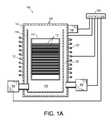
- FIG. 1Ashows a simplified block diagram of a batch processing system for forming a high-k dielectric film on a substrate according to an embodiment of the invention.
- the batch processing system 100includes a process chamber 102 , a gas injection system 104 , a heater 122 , a vacuum pumping system 106 , a process monitoring system 108 , and a controller 124 .
- Multiple substrates 110can be loaded into the process chamber 102 and processed using substrate holder 112 , also referred to as a wafer boat.
- the process chamber 102comprises an outer section 114 and an inner section 116 .
- the inner section 116can be a process tube.
- the batch processing systemis capable of fast temperature ramping (lowering or raising) over a large temperature range.
- Temperature ramp ratesmay be a function of the difference between initial and final temperature.
- the temperature ramp ratemay be as high as 50° C./min, for example when ramping the temperature over a large temperature range (e.g., ramping from 250° C. to 800° C.).
- the temperature ramp ratemay be in the range of 5-20° C./min if the difference between initial and final temperature is relatively small (e.g., ramping from 250° C. to 300° C.), in order to avoid overshooting the final temperature.
- the gas injection system 104can introduce gases into the process chamber 102 for purging the process chamber 102 , and for preparing, cleaning, and processing the substrates 110 .
- the gas injection system 104can, for example, include a liquid delivery system (LDS) (not shown) that contains a vaporizer to vaporize a precursor liquid.
- LDSliquid delivery system
- the vaporized liquidcan be flowed into the process chamber 102 with or without the aid of a carrier gas.
- the gas injection systemcan include a bubbling system where the carrier gas is bubbled through a reservoir containing the precursor liquid.
- embodiments of the inventionmay utilize a wide variety of hafnium and zirconium precursors for forming hafnium(Hf)- or zirconium(Zr)-containing films.
- representative examplesinclude: Hf(O t Bu) 4 (hafnium tert-butoxide, HTB), Hf(NEt 2 ) 4 (tetrakis(diethylamido)hafnium, TDEAH), Hf(NEtMe) 4 (tetrakis(ethylmethylamido)hafnium, TEMAH), Hf(NMe 2 ) 4 (tetrakis(dimethylamido)hafnium, TDMAH), Zr(O t Bu) 4 (zirconium tert-butoxide, ZTB), Zr(NEt 2 ) 4 (tetrakis(diethylamido)zirconium, TDEAZ), Zr(NMeEt) 4 (tetrakis(e
- Ta-containing precursors containing “Ta—N” intra-molecular bondsinclude, for example, TAIMATA, Ta(NEt 2 ) 5 (PDEAT), Ta(NMe 2 ) 5 (PDMAT), Ta(NEtMe) 5 (PEMAT), ( t BuN)Ta(NMe 2 ) 3 (TBTDMT), ( t BuN)Ta(NEt 2 ) 3 (TBTDET), ( t BuN)Ta(NEtMe) 3 (TBTEMT), and ( i PrN)Ta(NEt 2 ) 3 (IPTDET).
- TAIMATATa(NEt 2 ) 5 (PDEAT), Ta(NMe 2 ) 5 (PDMAT), Ta(NEtMe) 5 (PEMAT), ( t BuN)Ta(NMe 2 ) 3 (TBTDMT), ( t BuN)Ta(NEt 2 ) 3 (TBTDET), ( t BuN)Ta(NEtMe) 3 (TBTEMT), and ( i PrN
- Ta-containing precursors containing “Ta—C” intra-molecular bondsinclude, for example, Ta( ⁇ 5 -C 5 H 5 ) 2 H 3 , Ta(CH 2 )(CH 3 )( ⁇ 5 -C 5 H 5 ) 2 , Ta( ⁇ 3 -C 3 H 5 )( ⁇ 5 -C 5 H 5 ) 2 , Ta(CH 3 ) 3 ( ⁇ 5 -C 5 H 5 ) 2 , Ta(CH 3 ) 4 ( ⁇ 5 -C 5 (CH 3 ) 5 ), or Ta( ⁇ 5 -C 5 (CH 3 ) 5 ) 2 H 3 .
- Ti-containing precursors having “Ti—N” intra-molecular bondsinclude, for example, Ti(NEt 2 ) 4 (TDEAT), Ti(NMeEt) 4 (TEMAT), Ti(NMe 2 ) 4 (TDMAT).
- Ti-containing precursors containing “Ti—C” intra-molecular bondsinclude, for example, Ti(COCH 3 )( ⁇ 5 -C 5 H 5 ) 2 Cl, Ti( ⁇ 5 -C 5 H 5 )Cl 2 , Ti( ⁇ 5 -C 5 H 5 )Cl 3 , Ti( ⁇ 5 -C 5 H 5 ) 2 Cl 2 , Ti( ⁇ 5 -C 5 (CH 3 ) 5 )Cl 3 , Ti(CH 3 )( ⁇ 5 -C 5 H 5 ) 2 Cl, Ti( ⁇ 5 -C 9 H 7 ) 2 Cl 2 , Ti(( ⁇ 5 -C 5 (CH 3 ) 5 ) 2 Cl, Ti(( ⁇ 5 -C 5 (CH 3 ) 5 ) 2 Cl
- aluminum-containing precursorsinclude, for example, Al 2 Me 6 , Al 2 Et 6 , AI(CH 3 COCHCOCH 3 ) 3 , AlBr 3 , All 3 , Al(O i Pr) 3 , [Al(NMe 2 ) 3 ] 2 , Al( i Bu) 2 Cl, Al( i Bu) 3 , Al( i Bu) 2 H, AlEt 2 Cl, and Al(THD) 3 .
- Embodiments of the inventionsmay utilize a wide variety of different rare earth precursors to form a high-k dielectric film.
- Examples of rare earth precursorare described in U.S. patent application Ser. No. 11/278,387, the entire content of which is hereby incorporated by reference.
- the high-k dielectric filmcan contain a rare earth metal as a metal oxide, a metal oxynitride, a metal silicate, or a metal silicon oxynitride, or a combination thereof.
- ligand notationt Bu:tert-butyl, i Bu:iso-butyl, Et:ethyl, Me:methyl, Cp:cyclopentadienyl, i Pr:isopropyl, and THD: 2,2,6,6-tetramethyl-3,5-heptanedionate.
- the gas injection system 104can be configured for flowing a gaseous Si-containing gas (e.g., silane (SiH 4 )), an oxidizer containing an oxygen-containing gas or an oxygen- and nitrogen-containing gas (e.g., O 2 , O 3 , N 2 O, NO, or H 2 O vapor) into the process chamber 102 .
- the oxidizer gas sourcemay include a water vapor generator (WVG) (not shown) that generates H 2 O vapor from H 2 gas and O 2 gas.
- WVGwater vapor generator
- a WVGis a high-dilution pyrogenic torch developed by Tokyo Electron Ltd., Nirasaki, Yamanashi, Japan.
- the high-dilution pyrogenic torchcombusts small flows of H 2 gas and O 2 gas to generate H 2 O vapor in the form of steam, external to the process chamber 102 .
- the above-mentioned gas flowscan, for example, contain an inert gas (e.g., a noble gas or N 2 ) and/or a hydrogen-containing gas.
- the hydrogen-containing gascan, for example, contain H 2 .
- a plurality of gas supply linescan be arranged to flow gases into the process chamber 102 .
- the gasescan be introduced into volume 118 , defined by the inner section 116 , and exposed to substrates 110 . Thereafter, the gases can flow into the volume 120 , defined by the inner section 116 and the outer section 114 , and exhausted from the process chamber 102 by the vacuum pumping system 106 .
- Substrates 110can be loaded into the process chamber 102 and processed using substrate holder 112 .
- the batch processing system 100can allow for a large number of tightly stacked substrates 110 to be processed, thereby resulting in high substrate throughput.
- a substrate batch sizecan, for example, be about 100 substrates (wafers), or less. Alternately, the batch size can be about 25 substrates, or less.
- the process chamber 102can, for example, process a substrate of any size, for example 200 mm substrates, 300 mm substrates, or even larger substrates.
- the substrates 110can, for example, comprise semiconductor substrates (e.g. silicon or compound semiconductor), LCD substrates, and glass substrates.
- the batch processing system 100can be controlled by a controller 124 capable of generating control voltages sufficient to communicate and activate inputs of the batch processing system 100 as well as monitor outputs from the batch processing system 100 .
- the controller 124can be coupled to and exchange information with process chamber 102 , gas injection system 104 , heater 122 , process monitoring system 108 , and vacuum pumping system 106 .
- a program stored in the memory of the controller 124can be utilized to control the aforementioned components of the batch processing system 100 according to a stored process recipe.
- Real-time process monitoringcan be carried out using process monitoring system 108 .
- the process monitoring system 108is a versatile monitoring system and can, for example, comprise a mass spectrometer (MS) or a Fourier Transform Infra-red (FTIR) spectrometer.
- MSmass spectrometer
- FTIRFourier Transform Infra-red
- the process monitoring system 108can provide qualitative and quantitative analysis of the gaseous chemical species in the process environment.
- Process parameters that can be monitoredinclude gas flows, gas pressure, ratios of gaseous species, and gas purities. These parameters can be correlated with prior process results and various physical properties of the deposited high-k dielectric film.
- FIG. 1Bshows a simplified block diagram of another batch processing system for forming a high-k dielectric film on a substrate according to an embodiment of the invention.
- the batch processing system 1contains a process chamber 10 and a process tube 25 that has an upper end 23 connected to a exhaust pipe 80 , and a lower end hermetically joined to a lid 27 of cylindrical manifold 2 .
- the exhaust pipe 80discharges gases from the process tube 25 to a vacuum pumping system 88 to maintain a pre-determined atmospheric or below atmospheric pressure in the processing system 1 .
- a substrate holder 35 for holding a plurality of substrates (wafers) 40 in a tier-like manner (in respective horizontal planes at vertical intervals)is placed in the process tube 25 .
- the substrate holder 35resides on a turntable 26 that is mounted on a rotating shaft 21 penetrating the lid 27 and driven by a motor 28 .
- the turntable 26can be rotated during processing to improve overall film uniformity or, alternately, the turntable can be stationary during processing.
- the lid 27is mounted on an elevator 22 for transferring the substrate holder 35 in and out of the process tube 25 . When the lid 27 is positioned at its uppermost position, the lid 27 is adapted to close the open end of the manifold 2 .
- a plurality of gas supply linescan be arranged around the manifold 2 to supply a plurality of gases into the process tube 25 through the gas supply lines.
- FIG. 1Bonly one gas supply line 45 among the plurality of gas supply lines is shown.
- the gas supply line 45is connected to a gas injection system 94 .
- a cylindrical heat reflector 30is disposed so as to cover the process tube 25 .
- the heat reflector 30has a mirror-finished inner surface to suppress dissipation of radiation heat radiated by main heater 20 , bottom heater 65 , top heater 15 , and exhaust pipe heater 70 .
- a helical cooling water passage(not shown) is formed in the wall of the process chamber 10 as a cooling medium passage.
- a vacuum pumping system 88comprises a vacuum pump 86 , a trap 84 , and automatic pressure controller (APC) 82 .
- the vacuum pump 86can, for example, include a dry vacuum pump capable of a pumping speed up to 20,000 liters per second (and greater).
- gasescan be introduced into the process chamber 10 via the gas injection system 94 and the process pressure can be adjusted by the APC 82 .
- the trap 84can collect unreacted precursor material and by-products from the process chamber 10 .
- the process monitoring system 92comprises a sensor 75 capable of real-time process monitoring and can, for example, comprise a MS or a FTIR spectrometer.
- a controller 90includes a microprocessor, a memory, and a digital I/O port capable of generating control voltages sufficient to communicate and activate inputs to the processing system 1 as well as monitor outputs from the processing system 1 .
- the controller 90is coupled to and can exchange information with gas injection system 94 , motor 28 , process monitoring system 92 , heaters 20 , 15 , 65 , and 70 , and vacuum pumping system 88 .
- FIG. 2depicts a gas injection system 200 coupled to a process chamber 190 , where the gas injection system 200 and process chamber 190 can be the gas injection system 104 and process chamber 102 in FIG. 1A or the gas injection system 94 and process chamber 10 in FIG. 1B .
- Gas injection system 200can be coupled to a liquid delivery system (LDS) 202 that contains a vaporizer to vaporize a precursor liquid such as tert-butoxide (HTB) and tetra-diethylamide hafnium (TDEAH).
- FIG. 3depicts the chemical structures and formulas for HTB or TDEAH.
- the vaporized liquidcan be flowed through the gas injection system 200 into the process chamber 190 with or without the aid of a carrier gas.
- a bubbling system 204may be provided where the carrier gas is bubbled through a reservoir containing the precursor liquid.
- the gas injection system 200can be coupled to a Si-containing gas source 206 , e.g., SiCl 4 , SiH 4 , or Si 2 H 6 , to provide a Si-containing gas to the process chamber 190 to incorporate Si into the high-k dielectric film.
- Gas injection system 200may also include an oxidizing gas source 208 , for example a water vapor generator (WVG) or an ozone generator.
- WVGwater vapor generator
- Gas injection system 200may also include a N-containing gas source 210 , e.g., NH 3 , to provide a N-containing gas to the process chamber to incorporate N into the high-k dielectric film.
- a N-containing gas source 210e.g., NH 3
- a plurality of gas supply lines 212 , 214 , 216 , 218can be arranged to flow the gases into the process chamber 190 .
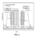
- FIG. 4graphically depicts a timeline for in-situ hybrid deposition of a high-k dielectric film using a combination of ALD and CVD according to an embodiment of the invention
- FIGS. 5A-5Eshow a schematic cross-sectional representation of a process flow for an in-situ hybrid deposition of a high-k dielectric film on a substrate according to an embodiment of the invention.
- the timelineshows an optional pre-treating of a substrate, deposition of a first portion of a high-k dielectric film on the substrate, deposition of a second portion of the high-k dielectric film on the first portion by CVD to form the high-k dielectric film, and an optional post-treating of the high-k dielectric film.
- the pre-treating, the post-treating, or both the pre-treating and the post-treatingare may be omitted from the overall in-situ hybrid deposition process depicted in FIG. 4 and FIGS. 5A-5E .
- the process steps shown in FIG. 4i.e., pre-treating, ALD, CVD, and post-treating
- the in-situ hybrid high-k dielectric film deposition processincludes providing plurality of substrates to be processed, for example 25 or 50 substrates, on a substrate holder in a process chamber of a batch processing system maintained at a temperature T 1 .
- a process chamber of a batch processing systemmaintained at a temperature T 1 .
- the process chamber temperaturewill be at or near the substrate temperature.
- the process chamberis evacuated and optionally purged with an inert gas.
- the in-situ hybrid high-k dielectric film deposition processcan save time on loading and removing substrates since the substrates only need to be loaded once prior to pre-treating and removed from the process chamber once after post-treating.
- the processsaves time on temperature ramping, since the substrates do not need be cooled down to a transfer temperature between steps.
- the processsaves time on substrate transport by eliminating the transport steps between each process step. In addition to the time-savings, the process reduces opportunities for contamination of the high-k dielectric film and contamination of an interface layer between the substrate and the high-k dielectric film.
- a pre-treating of the substratesmay be performed prior to depositing a high-k dielectric film on the substrates.
- the pre-treatingmay be performed to remove impurities from a surface of the substrate 500 depicted in FIG. 5A and subsequently form an oxide or oxynitride interface layer 502 on the substrate 500 as depicted in FIG. 5B .
- a thickness of the interface layer 502can be, for example, between about 0.4 nm and about 2 nm, or between about 0.8 nm and about 1.5 nm.
- the oxide or oxynitride interface layer 502may be present on the substrate 500 when the substrate 500 is loaded into the process chamber.
- the interface layer 502may be absent from the substrate 500 .
- the pre-treatingcan include ramping the substrate temperature from T 1 (e.g., approximately room temperature) to T 2 and exposing the substrate 500 to a gaseous oxidizer for a pre-determined amount of time at T 2 .
- the pre-treatingmay be performed for about 30 seconds up to about 30 minutes, or between about 5 minutes and about 20 minutes, for example about 10 minutes.
- the oxidizeroxygen-containing gas or oxygen- and nitrogen-containing gas
- the oxidizermay further contain an inert gas such as Ar or nitrogen N 2 .
- a water vapor generatormay be used to generate water vapor (H 2 O) and deliver (or pulse) it to the process chamber.
- the substrate temperature T 2can be between about 200° C. and about 1000° C. during the pre-treating, between about 400° C. and about 900° C., or between about 500° C. and about 850° C.
- the chamber pressurecan be in between about 0.01 mTorr and about 100 Torr, for example between about 0.1 Torr and about 10 Torr.
- One exemplary pre-treatingincludes exposing the substrate 500 to NO at a substrate temperature T 2 between about 700° C. and about 800° C.
- a flow rate for the NO oxidizermay be up to about 20 slm, for example about 0.1-5 slm.
- the substrate temperatureis ramped from T 2 to T 3 and a first portion 504 of a high-k dielectric film depicted in FIG. 5C is deposited on the interface layer 502 by ALD.
- the first portion 504may be directly deposited on the substrate 500 , for example when a pre-treating is omitted.
- T 3is lower than T 2 .
- T 3may be equal to T 2 , or T 3 make be higher than T 2 .
- the ALDmay be carried out under same or similar temperature and pressure conditions as the optional pre-treating step described above.
- a thickness of the first portion 504 of the high-k dielectric filmcan, for example, be between 0.5 nm and about 5 nm.
- the ALDprovides a relatively slow growth rate of the conformal first portion 504 with excellent interface properties with the underlying interface layer 502 or substrate 500
- ALDhas demonstrated an outstanding ability to maintain ultra-uniform thin deposition film on flat surfaces or over complex surface topology. This is at least partially because ALD is not as flux dependent as is CVD processing.
- the technique of ALDis based on the principle of the formation of a saturated monolayer or sub-monolayer of reactive precursor molecules (metal precursor) by chemisorption.
- a typical ALD cycle for forming an AB layerincludes flowing a precursor or reactant A into a process chamber for a period of time in which a saturated monolayer of A is formed on the substrate. Then, the flow of precursor or reactant A is stopped and the precursor or reactant A is evacuated and/or purged from the process chamber using an inert gas, G I .
- precursor or reactant Bis followed by flowing precursor or reactant B into the process chamber, also for a period of time, to combine B with A thus forming the layer AB on the substrate. Then, the flow of precursor or reactant B is stopped and the precursor or reactant B is evacuated and/or purged from the process chamber using inert gas, G I .
- This process of introducing precursor or reactant A, purging the process chamber, introducing precursor or reactant B, and purging the process chambercan be repeated a number of times to achieve an AB film (i.e., first portion 504 of the high-k dielectric film) of a desired thickness. The number of cycles, the flow rates, and exposure times may be dependent, at least in part, upon the desired AB film thickness.
- the evacuation and/or purge timesare dependent on the process chamber volume and design, and chemicals used as well as the process pressure and gas flow rates.
- the ALDmay include about 5-50 cycles of alternating pulsing of an oxidizer (e.g., O 2 or H 2 O) and a metal precursor (e.g., TDEAH), for example about 10-25 cycles.
- the exposure (or pulsing) time for the oxidizer and the metal precursormay each be in the range of about 5 seconds to about 5 minutes, for example about 15 seconds to about 2 minutes.
- the oxidizermay be pulsed for twice as long as the hafnium precursor.
- the evacuation times and/or purge timesmay be any desired time for removing excess reactant from the chamber, for example, about 10 seconds to about 5 minutes, and by way of further example, about 30 seconds to about 2 minutes.
- the substrate temperatureis lowered from T 3 to T 4 and a second portion 506 of the high-k dielectric film 508 depicted in FIG. 5D is deposited by CVD processing on the first portion 504 at a substrate temperature T 4 .
- the first and second portions 504 and 506form high-k dielectric film 508 .
- precursors or reactants A and Bare both flowed into the process chamber for a time period selected for depositing the second portion 506 with a desired thickness.
- a thickness of the second portion 506can, for example, be between 1 nm and about 100 nm.
- T 4is lower than T 3 .
- T 4may be equal to T 3 , or T 4 make be higher than T 3 .
- the CVD processingmay be carried out under same or similar temperature and pressure conditions as the ALD described above.
- the CVDprovides a high growth rate of the second portion 506 on the first portion 504 of the high-k dielectric film 508 .
- the in-situ hybrid high-k dielectric deposition processcombines superior conformality and interface properties of the first portion 504 deposited by ALD and high deposition rates of the second portion 506 deposited by CVD. This enables cost-effective formation of a wide variety of high-quality high-k dielectric films found or proposed in advanced semiconductor devices.
- a total thickness of the high-k dielectric film 508may be chosen by independently selecting a thickness of the first portion 504 and a thickness of the second portion 506 .
- the thickness of the first portion 504is a function of the total number of ALD cycles and a thickness of the second portion 506 is a function of the total exposure time of the oxidizer and the metal precursor.
- the in-situ hybrid high-k dielectric deposition processmay include performing ALD using a first set of process conditions (e.g., ALD substrate temperature, ALD gas pressure, and ALD gas flows), adjusting the process conditions to a second set of process conditions (e.g., CVD substrate temperature, CVD gas pressure, and CVD gas flows), and performing CVD using the second set of process conditions.
- ALDatomic layer deposition
- an optional post-treating of the high-k dielectric film 508may be performed at a substrate temperature T 5 to form modified high-k dielectric film 510 depicted in FIG. 5E .
- T 5is higher than T 4 .
- T 5may be equal to T 4 , or T 5 may be lower than T 4 .
- the post-treatingcan densify the high-k dielectric film 508 , remove unreacted reactants from the high-k dielectric film 508 , further oxidize the interface layer 502 , or fill oxygen vacancies and or redistribute substitutional oxygen in the high-k dielectric film 508 .
- the post-treatingmay include (a) a high temperature anneal at a substrate temperature between about 500° C. and about 1000° C. with no gaseous environment (i.e., high vacuum condition), (b) a high temperature oxidation at substrate temperature between about 500° C. and about 1000° C. in the presence of a fourth oxidizer selected from an oxygen-containing gas or an oxygen- and nitrogen-containing gas, or (c) a high temperature anneal at a substrate temperature between about 500° C. and about 1000° C. in the presence of a non-oxidizing gas (e.g., an inert gas such as argon (Ar) or nitrogen (N 2 )).
- a non-oxidizing gase.g., an inert gas such as argon (Ar) or nitrogen (N 2 )
- the post-treatingmay be performed under same or similar conditions as the pre-treating, but this is not required as other processing conditions may be utilized.
- the post-treatingcan include ramping the substrate temperature from T 4 to T 5 and performing the post-treating for a pre-determined amount of time at T 5 .
- the post-treatingmay include exposure to an inert gas for a first time period, followed by exposure to an oxidizer for a second time period.
- the post-treatingmay include exposure to an oxidizer for a first time period, followed by exposure to an inert gas for a second time period.
- the pre-treatingmay be performed for about 30 seconds up to about 30 minutes, or between about 5 minutes and about 20 minutes, for example about 10 minutes.
- the oxidizercan include O 2 , O 3 , N 2 O, NO, or H 2 O, or a combination thereof.
- the substrate temperaturecan be between about 200° C. and about 1000° C. during the post-treating, between about 400° C. and about 900° C., or between about 500° C. and about 850° C.
- the chamber pressurecan be in between about 0.01 mTorr and about 100 Torr, for example between about 0.1 and about 10 Torr.
- One exemplary post-treatingincludes exposing the high-k dielectric film 508 to NO at a temperature between about 700° C. and about 800° C.
- the post-treatingmay be performed after deposition of the first portion 504 and before deposition of the second portion 506 .
- the temperatures T 1 -T 5may have any value between 200° C. and 1000° C., but higher and lower temperatures may also be selected. Although frequent temperature ramping may be required between ALD and CVD, in addition to any optional pre-treating and/or post-treating, the fast temperature ramping capabilities and short temperature stabilization periods can attain high substrate throughput.
- the pressure in the process chambermay be the same or similar throughout the optional pre-treating, the ALD, the CVD, and the optional post-treating. Alternatively, the pressure may vary.
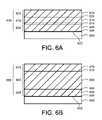
- FIGS. 6A and 6Bshow schematic cross-sectional representations of additional high-k dielectric films deposited on substrates according to embodiments of the invention.
- the alternating ALD and CVDmay be repeated any number of times to better control the conformality and electrical film properties of the resulting high-k dielectric film.
- a plurality of first film portions deposited by ALDmay be interspersed at substantially equal intervals in a relatively thick second film portions deposited by CVD.
- FIG. 6Ashows an exemplary high-k dielectric film 638 on an interface layer 602 overlying a substrate 600 .
- the high-k dielectric film 638contains first, second, and third high-k dielectric films 608 , 618 , and 628 , respectively.
- First high-k dielectric film 608contains a first portion 604 deposited by ALD and a second portion 606 deposited by CVD.
- the second and third high-k dielectric films 618 , 628contain first portions 614 , 624 deposited by ALD and second portions 616 , 626 deposited by CVD. As schematically depicted in FIG.
- the first portions 604 , 614 , 624have the same or substantially the same thickness and are interspersed in the high-k dielectric film 638 at substantially equal intervals.
- the hybrid high-k dielectric film deposition processis not limited to three high-k dielectric films as depicted in FIG. 6A , as any number of high-k dielectric films may be deposited.
- a 40 nm thick high-k dielectric filmmay be deposited using 8 deposition sequences, where each deposition sequence deposits a high-k dielectric film with a thickness of 1 nm by ALD and deposits a high-k dielectric film with a thickness of 4 nm by CVD.
- FIG. 6Bshows another exemplary high-k dielectric film 688 on an interface layer 652 overlying a substrate 650 .
- the high-k dielectric film 688contains first, second, and third high-k dielectric films 658 , 668 , and 678 , respectively.
- First high-k dielectric film 658contains a first portion 654 deposited by ALD and a second portion 656 deposited by CVD.
- the second and third high-k dielectric films 668 , 678contain first portions 664 , 674 deposited by ALD and second portions 666 , 676 deposited by CVD. As schematically depicted in FIG.
- the first portions 654 , 664 , and 674have the same or substantially the same thickness but the second high-k dielectric film 668 has a substantially thicker second (CVD) portion 666 than the corresponding first (CVD) portions 656 , 676 in the first and third high-k dielectric films 658 , 678 , respectively.
- the hybrid high-k dielectric film deposition processmay be utilized for depositing a wide variety of different high-k dielectric films containing any number of first and second portions, where the first and second portions can each have any desired thickness.
- the hybrid high-k dielectric film deposition processis not limited to three high-k dielectric films as depicted in FIG. 6B , as any number of high-k dielectric films may be deposited with any thickness.
- a benefit of depositing a portion of a high-k dielectric film by ALDcan include blocking or breaking up film defects that may significantly contribute to the increase in leakage current of the entire high-k dielectric films 638 and 688 . Therefore, the electrical properties of the high-k dielectric films 638 and 688 may be improved with careful use of ALD, while the bulk of the high-k dielectric films 638 and 688 may be deposited using the more economical CVD.
- the post-treating described in reference to FIGS. 5A-5Emay also be performed after deposition of the first portions 604 , 614 and 624 and before deposition of the second portions 606 , 616 and 626 , respectively.
- the first portion 604may be post-treated before deposition of the second portion 606 .
- the post-treatingmay be performed after deposition of the first portions 654 , 664 and 674 and before deposition of the second portions 656 , 666 and 676 , respectively
- Table 1shows results for deposition of a HfO 2 film on a substrate in a batch processing system by CVD, ALD, and ALD followed by CVD.
- Table 1shows deposition method (including type of oxidizer), substrate temperature, total run (deposition) time, EOT, dielectric constant (k), flat band voltage shift ( ⁇ V fb ), interface state density (D it ), and leakage current density (J L ) at ⁇ 2 Volts, ⁇ 6 Volts, and ⁇ 8 Volts.
- the ALDused alternating exposures of H 2 O oxidizer and TDEAH hafnium precursor at substrate temperatures of 275° C. and 300° C., where the alternating exposures were separated by evacuation and purging steps. The 275° C.
- ALD processincluded 160 cycles and the 300° C.
- ALD processincluded 65 cycles.
- Each ALD cycleincluded H 2 O oxidizer exposure time of 30 seconds and TDEAH exposure time 90 seconds.
- Each ALD cyclefurther included a 1 minute gas purge, followed by a 1 minute evacuation, after each H 2 O oxidizer exposure and TDEAH exposure.
- the process chamber pressurewas 0.3 Torr during the ALD processes.
- the H 2 O oxidizerwas generated in a water vapor generator using a gas flow rate of 0.1 standard liters per minute (slm) of H 2 and 0.1 slm of O 2 . The alternating exposures were carried out until the desired physical thickness of the HfO 2 film was achieved.
- the CVDused simultaneous exposures of O 2 oxidizer and TDEAH at substrate temperatures of 235° C. and 250° C.
- the process chamber pressurewas 0.3 Torr during the CVD processes.
- the O 2 oxidizer gas flow ratewas 0.5 slm
- the TDEAH exposureincluded a gas flow rate of 1.25 slm of N 2 carrier gas into a TDEAH vaporizer with 0.1 cubic centimeter (cc)/min of TDEAH liquid concurrently delivered to the vaporizer.
- deposition of the high-k dielectric films by ALDwas significantly slower than the deposition by CVD. This is due, at least in part, to the separation required for the reactant gases H 2 O and TDEAH, and the purge gas, in ALD.
- ALDis often used or preferred over CVD because of the ability of ALD to deposit thin films with uniform thickness in deep trenches and on structures with complex surface topography compared to CVD.
- high-k dielectric films deposited by ALDoften exhibit superior electrical properties due, at least in part, lower film defects.
- Table 1further shows the results of an in-situ hybrid HfO 2 deposition process according to an embodiment of the invention.
- the in-situ hybrid deposition processincluded sequential deposition of a HfO 2 film by ALD and CVD.
- the ALDused alternating exposures of a H 2 O oxidizer and a TDEAH hafnium precursor at a substrate temperature of 275° C., separated by evacuation and purging steps.
- the ALD processincluded 70 cycles and the ALD process was followed by a 40 min CVD process.
- the ALD and CVD processing conditionshave been described above. Next, the temperature was ramped from 275° C. to 235° C. at a rate of 5° C./min.
- the CVD processingused simultaneous exposures of the O 2 oxidizer and the TDEAH hafnium precursor at substrate temperature of 235° C.
- the hybrid in-situ HfO 2 deposition processprovides the compromise of shorter run time compared to ALD alone and HfO 2 film electrical properties that are improved over CVD alone.
Landscapes
- Chemical & Material Sciences (AREA)
- Engineering & Computer Science (AREA)
- Chemical Kinetics & Catalysis (AREA)
- General Chemical & Material Sciences (AREA)
- Organic Chemistry (AREA)
- Metallurgy (AREA)
- Mechanical Engineering (AREA)
- Materials Engineering (AREA)
- Condensed Matter Physics & Semiconductors (AREA)
- Power Engineering (AREA)
- Microelectronics & Electronic Packaging (AREA)
- Computer Hardware Design (AREA)
- Manufacturing & Machinery (AREA)
- General Physics & Mathematics (AREA)
- Physics & Mathematics (AREA)
- Inorganic Chemistry (AREA)
- Formation Of Insulating Films (AREA)
- Chemical Vapour Deposition (AREA)
Abstract
Description
- The present invention is related to U.S. patent application Ser. No. 11/462,234, filed Aug. 3, 2006 and entitled IN-SITU ATOMIC LAYER DEPOSITION. The entire content of this application is incorporated herein by reference.
- This invention relates to deposition of high dielectric constant (high-k) dielectric films for microelectronic devices, and more particularly to an in-situ hybrid deposition of high-k dielectric films using a combination of atomic layer deposition (ALD) and chemical vapor deposition (CVD).
- In the semiconductor industry, the minimum feature sizes of microelectronic devices are well into the deep sub-micron regime to meet the demand for faster, and lower power semiconductor devices. The downscaling of complimentary metal-oxide-semiconductor (CMOS) devices imposes scaling constraints on the gate dielectric material. The thickness of the conventional SiO2gate dielectric is approaching its physical limits. The most advanced devices are using nitrided SiO2gate dielectrics approaching an equivalent oxide thickness (EOT) of about 1 nanometer (nm) or less where the leakage current density can be as much as 1 mA/cm2. To improve device reliability and reduce electrical leakage from the gate dielectric to the transistor channel during operation of the device, semiconductor transistor technology is implementing the use of high-k gate dielectric materials that allow increased physical thickness of the gate dielectric layer while maintaining a low EOT. EOT is defined as the thickness of SiO2that would produce the same capacitance voltage curve as that obtained from an alternate dielectric material. High-k materials are dielectric materials featuring a dielectric constant greater than that of SiO2(k˜3.9). High-k materials may refer to dielectric materials that are deposited onto substrates rather than grown on the surface of the substrate, as is the case for SiO2. High-k materials may, for example, include a metal oxide film or a metal silicate film.
- Several methods have been developed for forming thin high-k dielectric films that may be used in semiconductor devices. Among the more established techniques are Chemical Vapor Deposition (CVD) and Atomic Layer Deposition (ALD), but these deposition techniques each have advantages and disadvantages that are problematic for high-volume semiconductor manufacturing. In addition to the need to reduce substrate (wafer) contamination, there is further a need to achieve good uniformity in batch processing, with respect to zone-to-zone uniformity, wafer-to-wafer uniformity and overall film uniformity. In addition to the need for good film uniformity, there is also a need to improve the electrical properties of the high-k dielectric film, including the amount of hysteresis in the film, the density of defects at interfaces of the high-k dielectric film with other materials, and the leakage current, while maintaining a high effective k value for the film stack and a low EOT.
- Embodiments of the invention provide a method for in-situ hybrid deposition of a high-k dielectric film on a plurality of substrates for high-volume semiconductor manufacturing. The method includes sequential deposition of the high-k dielectric film using atomic layer deposition (ALD) and chemical vapor deposition (CVD). The portion of the high-k dielectric film deposited by ALD forms an excellent interface with the underlying substrate or an interface layer on the substrate, and the portion of the high-k dielectric film deposited by CVD uses the benefit of the higher deposition rate of CVD to provide cost-effective formation of a high-quality high-k dielectric film. Furthermore, the batch processing system is capable of fast temperature ramping (lowering or raising) over a large temperature range, thereby enabling the deposition of the first and second portions to be performed at different substrate temperatures.
- According to one embodiment of the invention, the method includes loading a plurality of substrates into a process chamber of a batch processing system; depositing a first portion of a high-k dielectric film on the plurality of substrates by atomic layer deposition (ALD); after depositing the first portion, and without removing the plurality of substrates from the process chamber, depositing a second portion of the high-k dielectric film on the first portion by chemical vapor deposition (CVD); and removing the plurality of substrates from the process chamber. The method can further include pre-treating the substrates and post-treating the high-k dielectric films in-situ prior to the removing.
- A more complete appreciation of the invention and many of the attendant advantages thereof will become readily apparent with reference to the following detailed description, particularly when considered in conjunction with the accompanying drawings, in which:
FIG. 1A shows a simplified block diagram of a batch processing system according to an embodiment of the invention;FIG. 1B shows a simplified block diagram of another batch processing system according to an embodiment of the invention;FIG. 2 shows a simplified block diagram of a gas injection system coupled to a process chamber according to an embodiment of the invention;FIG. 3 depicts the chemical structures and formulas for hafnium tert-butoxide (HTB) and tetra-diethylamide hafnium (TDEAH);FIG. 4 graphically depicts a timeline for in-situ hybrid deposition of a high-k dielectric film using a combination of ALD and CVD according to an embodiment of the invention;FIGS. 5A-5E show a schematic cross-sectional representation of a process flow for an in-situ hybrid deposition of a high-k dielectric film on a substrate according to an embodiment of the invention; andFIGS. 6A and 6B show schematic cross-sectional representations of additional high-k dielectric films deposited on substrates according to embodiments of the invention.- Several methods have previously been developed for creating thin high-k dielectric films on substrates used in manufacturing semiconductor devices. Among the more established techniques is CVD. ALD, a variant of CVD, is a relatively newer technology now emerging as a potentially superior method of achieving uniform, conformal film deposition. ALD is a slower deposition method than CVD due to lower film deposition rates. However, ALD often provides superior high-k dielectric film properties such as better film conformality over high-aspect-ratio features such as trenches or vias commonly found in semiconductor devices, and reduced leakage currents due at least in part to better interfaces between the high-k dielectric film and underlying substrate and/or other films. Many uses of high-k dielectric films in semiconductor devices require film thicknesses that make ALD very time consuming due to the low film deposition rate and ALD can therefore be prohibitively expensive to perform. Furthermore, CVD processes, although being faster deposition processes, may not provide satisfactory high-k dielectric films due to inadequate film conformality and the inability to form good interfaces with an underlying substrate or/other films.
- Embodiments of the invention provide a method for in-situ hybrid deposition of a high-k dielectric film on a plurality of substrates using one or more alternating sequences of ALD and CVD in a batch processing system. According to some embodiments of the invention, the high-k dielectric film can include metal oxides, metal oxynitrides, metal silicates, or metal silicon oxynitrides, or a combination thereof. The high-k dielectric film may also contain impurities, for example carbon or a halogen. The high-k dielectric film can, for example, contain a hafnium-containing film (e.g., HfO2, HfON, HfSiO, or HfSiON), a zirconium-containing film (e.g., ZrO2, ZrON, ZrSiO, or ZrSiON), a tantalum-containing film (e.g., Ta2O5), a titanium-containing film (e.g., TiO2), or an aluminum-containing film (e.g., Al2O3), or a combination of two or more thereof. The high-k dielectric film may, for example, be utilized in a deep trench capacitor or as a part of a gate dielectric film in a transistor structure.
- One skilled in the relevant art will recognize that the various embodiments may be practiced without one or more of the specific details, or with other replacement and/or additional methods, materials, or components. In other instances, well-known structures or operations are not shown or described in detail to avoid obscuring aspects of various embodiments of the invention. Similarly, for purposes of explanation, specific numbers, and configurations are set forth in order to provide a thorough understanding of the invention. Nevertheless, the invention may be practiced without specific details. Furthermore, it is understood that the various embodiments shown in the figures are illustrative representations and are not necessarily drawn to scale.
- Reference throughout this specification to “one embodiment” or “an embodiment” means that a particular feature, structure, material, or characteristic described in connection with the embodiment is included in at least one embodiment of the invention, but do not denote that they are present in every embodiment. Thus, the appearances of the phrases “in one embodiment” or “in an embodiment” in various places throughout this specification are not necessarily referring to the same embodiment of the invention. Furthermore, the particular features, structures, or characteristics may be combined in any suitable manner in one or more embodiments. Various additional layers and/or structures may be included and/or described features may be omitted in other embodiments.
- Various operations will be described as multiple discrete operations in turn, in a manner that is most helpful in understanding the invention. However, the order of description should not be construed as to imply that these operations are necessarily order dependent. In particular, these operations need not be performed in the order of presentation. Operations described may be performed in a different order than the described embodiment. Various additional operations may be performed and/or described operations may be omitted in additional embodiments.
- According to one embodiment of the invention, a method of forming a high-k dielectric film includes first loading a plurality of substrates (wafers) into a process chamber (e.g., process tube) of a batch processing system, depositing a first portion of a high-k dielectric film on the plurality of substrates by ALD, and thereafter depositing a second portion of the high-k dielectric film on the first portion by CVD. According to embodiments of the invention, the entire in-situ hybrid (ALD followed by CVD) high-k dielectric film deposition process is performed without removing the substrates from the process chamber. This prevents or at least significantly reduces incorporation of many common contaminants (e.g., organic materials present in air) into the high-k dielectric film and provides excellent control over the material and electrical properties of the high-k dielectric film.
- According to other embodiments of the invention, the in-situ hybrid high-k dielectric film deposition process may further include pre-treating the substrate prior to depositing the high-k dielectric film on the substrate, post-treating the high-k dielectric film after deposition, or both pre-treating the substrate prior to the deposition of the high-k dielectric film and post-treating the high-k dielectric film after the deposition. The pre-treating may be performed to remove impurities from a surface of the substrate and/or to form an oxide or oxynitride interface layer on the substrate. The post-treating may be performed to densify and/or remove unreacted reactants from the high-k dielectric film, further form or oxidize the interface layer, or fill oxygen vacancies and or redistribute substitutional oxygen in the high-k dielectric film.
FIG. 1A shows a simplified block diagram of a batch processing system for forming a high-k dielectric film on a substrate according to an embodiment of the invention. Thebatch processing system 100 includes aprocess chamber 102, agas injection system 104, aheater 122, avacuum pumping system 106, aprocess monitoring system 108, and acontroller 124.Multiple substrates 110 can be loaded into theprocess chamber 102 and processed usingsubstrate holder 112, also referred to as a wafer boat. Furthermore, theprocess chamber 102 comprises anouter section 114 and aninner section 116. In one embodiment of the invention, theinner section 116 can be a process tube. The batch processing system is capable of fast temperature ramping (lowering or raising) over a large temperature range. Temperature ramp rates may be a function of the difference between initial and final temperature. The temperature ramp rate may be as high as 50° C./min, for example when ramping the temperature over a large temperature range (e.g., ramping from 250° C. to 800° C.). However, the temperature ramp rate may be in the range of 5-20° C./min if the difference between initial and final temperature is relatively small (e.g., ramping from 250° C. to 300° C.), in order to avoid overshooting the final temperature.- The
gas injection system 104 can introduce gases into theprocess chamber 102 for purging theprocess chamber 102, and for preparing, cleaning, and processing thesubstrates 110. Thegas injection system 104 can, for example, include a liquid delivery system (LDS) (not shown) that contains a vaporizer to vaporize a precursor liquid. The vaporized liquid can be flowed into theprocess chamber 102 with or without the aid of a carrier gas. For example, when a carrier gas is used, the gas injection system can include a bubbling system where the carrier gas is bubbled through a reservoir containing the precursor liquid. - For example, embodiments of the invention may utilize a wide variety of hafnium and zirconium precursors for forming hafnium(Hf)- or zirconium(Zr)-containing films. For example, representative examples include: Hf(OtBu)4(hafnium tert-butoxide, HTB), Hf(NEt2)4(tetrakis(diethylamido)hafnium, TDEAH), Hf(NEtMe)4(tetrakis(ethylmethylamido)hafnium, TEMAH), Hf(NMe2)4(tetrakis(dimethylamido)hafnium, TDMAH), Zr(OtBu)4(zirconium tert-butoxide, ZTB), Zr(NEt2)4(tetrakis(diethylamido)zirconium, TDEAZ), Zr(NMeEt)4(tetrakis(ethylmethylamido)zirconium, TEMAZ), Zr(NMe2)4(tetrakis(dimethylamido)zirconium, TDMAZ), ZrCp2Me2, Zr(tBuCp)2Me2, and Zr(NiPr2)4.
- Other embodiments may utilize a wide variety of tantalum, titanium, and aluminum precursors for forming tantalum(Ta)-, titanium(Ti)-, or aluminum(Al)-containing films. Examples of Ta-containing precursors containing “Ta—N” intra-molecular bonds include, for example, TAIMATA, Ta(NEt2)5(PDEAT), Ta(NMe2)5(PDMAT), Ta(NEtMe)5(PEMAT), (tBuN)Ta(NMe2)3(TBTDMT), (tBuN)Ta(NEt2)3(TBTDET), (tBuN)Ta(NEtMe)3(TBTEMT), and (iPrN)Ta(NEt2)3(IPTDET). Examples of Ta-containing precursors containing “Ta—C” intra-molecular bonds include, for example, Ta(η5-C5H5)2H3, Ta(CH2)(CH3)(η5-C5H5)2, Ta(η3-C3H5)(η5-C5H5)2, Ta(CH3)3(η5-C5H5)2, Ta(CH3)4(η5-C5(CH3)5), or Ta(η5-C5(CH3)5)2H3.
- Examples of Ti-containing precursors having “Ti—N” intra-molecular bonds include, for example, Ti(NEt2)4(TDEAT), Ti(NMeEt)4(TEMAT), Ti(NMe2)4(TDMAT). Examples of Ti-containing precursors containing “Ti—C” intra-molecular bonds include, for example, Ti(COCH3)(η5-C5H5)2Cl, Ti(η5-C5H5)Cl2, Ti(η5-C5H5)Cl3, Ti(η5-C5H5)2Cl2, Ti(η5-C5(CH3)5)Cl3, Ti(CH3)(η5-C5H5)2Cl, Ti(η5-C9H7)2Cl2, Ti((η5-C5(CH3)5)2Cl, Ti((η5-C5(CH3)5)2Cl2, Ti(η5-C5H5)2Cl2, Ti(η5-C5H5)2(CO)2, Ti(CH3)3(η5-C5H5), Ti(CH3)2(η5-C5H5)2, Ti(CH3)4, Ti(η5-C5H5)(η7-C7H7), Ti(η5-C5H5)(η8-C8H8), Ti(C5H5)2(η5-C5H5)2, Ti((C5H5)2)2(η-H)2, Ti(η5-C5(CH3)5)2, Ti(η5-C5(CH3)5)2(H)2, and Ti(CH3)2(η5-C5(CH3)5)2.
- Examples of aluminum-containing precursors include, for example, Al2Me6, Al2Et6, AI(CH3COCHCOCH3)3, AlBr3, All3, Al(OiPr)3, [Al(NMe2)3]2, Al(iBu)2Cl, Al(iBu)3, Al(iBu)2H, AlEt2Cl, and Al(THD)3.
- Embodiments of the inventions may utilize a wide variety of different rare earth precursors to form a high-k dielectric film. Examples of rare earth precursor are described in U.S. patent application Ser. No. 11/278,387, the entire content of which is hereby incorporated by reference. According to some embodiments of the invention, the high-k dielectric film can contain a rare earth metal as a metal oxide, a metal oxynitride, a metal silicate, or a metal silicon oxynitride, or a combination thereof.
- In the above description, the following ligand notation is used:tBu:tert-butyl,iBu:iso-butyl, Et:ethyl, Me:methyl, Cp:cyclopentadienyl,iPr:isopropyl, and THD: 2,2,6,6-tetramethyl-3,5-heptanedionate.
- In addition, the
gas injection system 104 can be configured for flowing a gaseous Si-containing gas (e.g., silane (SiH4)), an oxidizer containing an oxygen-containing gas or an oxygen- and nitrogen-containing gas (e.g., O2, O3, N2O, NO, or H2O vapor) into theprocess chamber 102. The oxidizer gas source (not shown) may include a water vapor generator (WVG) (not shown) that generates H2O vapor from H2gas and O2gas. One example of a WVG is a high-dilution pyrogenic torch developed by Tokyo Electron Ltd., Nirasaki, Yamanashi, Japan. The high-dilution pyrogenic torch combusts small flows of H2gas and O2gas to generate H2O vapor in the form of steam, external to theprocess chamber 102. Furthermore, the above-mentioned gas flows can, for example, contain an inert gas (e.g., a noble gas or N2) and/or a hydrogen-containing gas. The hydrogen-containing gas can, for example, contain H2. A plurality of gas supply lines can be arranged to flow gases into theprocess chamber 102. The gases can be introduced intovolume 118, defined by theinner section 116, and exposed tosubstrates 110. Thereafter, the gases can flow into thevolume 120, defined by theinner section 116 and theouter section 114, and exhausted from theprocess chamber 102 by thevacuum pumping system 106. Substrates 110 can be loaded into theprocess chamber 102 and processed usingsubstrate holder 112. Thebatch processing system 100 can allow for a large number of tightly stackedsubstrates 110 to be processed, thereby resulting in high substrate throughput. A substrate batch size can, for example, be about 100 substrates (wafers), or less. Alternately, the batch size can be about 25 substrates, or less. Theprocess chamber 102 can, for example, process a substrate of any size, for example 200 mm substrates, 300 mm substrates, or even larger substrates. Thesubstrates 110 can, for example, comprise semiconductor substrates (e.g. silicon or compound semiconductor), LCD substrates, and glass substrates.- The
batch processing system 100 can be controlled by acontroller 124 capable of generating control voltages sufficient to communicate and activate inputs of thebatch processing system 100 as well as monitor outputs from thebatch processing system 100. Moreover, thecontroller 124 can be coupled to and exchange information withprocess chamber 102,gas injection system 104,heater 122,process monitoring system 108, andvacuum pumping system 106. For example, a program stored in the memory of thecontroller 124 can be utilized to control the aforementioned components of thebatch processing system 100 according to a stored process recipe. - Real-time process monitoring can be carried out using
process monitoring system 108. In general, theprocess monitoring system 108 is a versatile monitoring system and can, for example, comprise a mass spectrometer (MS) or a Fourier Transform Infra-red (FTIR) spectrometer. Theprocess monitoring system 108 can provide qualitative and quantitative analysis of the gaseous chemical species in the process environment. Process parameters that can be monitored include gas flows, gas pressure, ratios of gaseous species, and gas purities. These parameters can be correlated with prior process results and various physical properties of the deposited high-k dielectric film. FIG. 1B shows a simplified block diagram of another batch processing system for forming a high-k dielectric film on a substrate according to an embodiment of the invention. Thebatch processing system 1 contains aprocess chamber 10 and aprocess tube 25 that has anupper end 23 connected to aexhaust pipe 80, and a lower end hermetically joined to alid 27 of cylindrical manifold2. Theexhaust pipe 80 discharges gases from theprocess tube 25 to avacuum pumping system 88 to maintain a pre-determined atmospheric or below atmospheric pressure in theprocessing system 1. Asubstrate holder 35 for holding a plurality of substrates (wafers)40 in a tier-like manner (in respective horizontal planes at vertical intervals) is placed in theprocess tube 25. Thesubstrate holder 35 resides on aturntable 26 that is mounted on arotating shaft 21 penetrating thelid 27 and driven by amotor 28. Theturntable 26 can be rotated during processing to improve overall film uniformity or, alternately, the turntable can be stationary during processing. Thelid 27 is mounted on anelevator 22 for transferring thesubstrate holder 35 in and out of theprocess tube 25. When thelid 27 is positioned at its uppermost position, thelid 27 is adapted to close the open end of the manifold2.- A plurality of gas supply lines can be arranged around the manifold2 to supply a plurality of gases into the
process tube 25 through the gas supply lines. InFIG. 1B , only onegas supply line 45 among the plurality of gas supply lines is shown. Thegas supply line 45 is connected to agas injection system 94. Acylindrical heat reflector 30 is disposed so as to cover theprocess tube 25. Theheat reflector 30 has a mirror-finished inner surface to suppress dissipation of radiation heat radiated bymain heater 20,bottom heater 65,top heater 15, andexhaust pipe heater 70. A helical cooling water passage (not shown) is formed in the wall of theprocess chamber 10 as a cooling medium passage. - A
vacuum pumping system 88 comprises a vacuum pump86, atrap 84, and automatic pressure controller (APC)82. The vacuum pump86 can, for example, include a dry vacuum pump capable of a pumping speed up to 20,000 liters per second (and greater). During processing, gases can be introduced into theprocess chamber 10 via thegas injection system 94 and the process pressure can be adjusted by theAPC 82. Thetrap 84 can collect unreacted precursor material and by-products from theprocess chamber 10. - The
process monitoring system 92 comprises asensor 75 capable of real-time process monitoring and can, for example, comprise a MS or a FTIR spectrometer. Acontroller 90 includes a microprocessor, a memory, and a digital I/O port capable of generating control voltages sufficient to communicate and activate inputs to theprocessing system 1 as well as monitor outputs from theprocessing system 1. Moreover, thecontroller 90 is coupled to and can exchange information withgas injection system 94,motor 28,process monitoring system 92,heaters vacuum pumping system 88. FIG. 2 depicts a gas injection system200 coupled to aprocess chamber 190, where the gas injection system200 andprocess chamber 190 can be thegas injection system 104 andprocess chamber 102 inFIG. 1A or thegas injection system 94 andprocess chamber 10 inFIG. 1B . Gas injection system200 can be coupled to a liquid delivery system (LDS)202 that contains a vaporizer to vaporize a precursor liquid such as tert-butoxide (HTB) and tetra-diethylamide hafnium (TDEAH).FIG. 3 depicts the chemical structures and formulas for HTB or TDEAH. The vaporized liquid can be flowed through the gas injection system200 into theprocess chamber 190 with or without the aid of a carrier gas. For example, when a carrier gas is used, a bubblingsystem 204 may be provided where the carrier gas is bubbled through a reservoir containing the precursor liquid. In addition, the gas injection system200 can be coupled to a Si-containing gas source206, e.g., SiCl4, SiH4, or Si2H6, to provide a Si-containing gas to theprocess chamber 190 to incorporate Si into the high-k dielectric film. Gas injection system200 may also include an oxidizinggas source 208, for example a water vapor generator (WVG) or an ozone generator. Gas injection system200 may also include a N-containinggas source 210, e.g., NH3, to provide a N-containing gas to the process chamber to incorporate N into the high-k dielectric film. A plurality ofgas supply lines process chamber 190.FIG. 4 graphically depicts a timeline for in-situ hybrid deposition of a high-k dielectric film using a combination of ALD and CVD according to an embodiment of the invention andFIGS. 5A-5E show a schematic cross-sectional representation of a process flow for an in-situ hybrid deposition of a high-k dielectric film on a substrate according to an embodiment of the invention. The timeline shows an optional pre-treating of a substrate, deposition of a first portion of a high-k dielectric film on the substrate, deposition of a second portion of the high-k dielectric film on the first portion by CVD to form the high-k dielectric film, and an optional post-treating of the high-k dielectric film. According to embodiments of the invention, the pre-treating, the post-treating, or both the pre-treating and the post-treating are may be omitted from the overall in-situ hybrid deposition process depicted inFIG. 4 andFIGS. 5A-5E . According to embodiments of the invention, the process steps shown inFIG. 4 (i.e., pre-treating, ALD, CVD, and post-treating) may be performed in-situ, i.e., in the same process chamber without removing the substrate from the process chamber.- The in-situ hybrid high-k dielectric film deposition process includes providing plurality of substrates to be processed, for example 25 or 50 substrates, on a substrate holder in a process chamber of a batch processing system maintained at a temperature T1. In the case of hot-wall process chambers, for example the
process chamber 102 inFIG. 1A or theprocess chamber 10 inFIG. 1B , in which cases the process chamber temperature will be at or near the substrate temperature. Following loading of the plurality of substrates into the process chamber, the process chamber is evacuated and optionally purged with an inert gas. - The in-situ hybrid high-k dielectric film deposition process can save time on loading and removing substrates since the substrates only need to be loaded once prior to pre-treating and removed from the process chamber once after post-treating. In addition, the process saves time on temperature ramping, since the substrates do not need be cooled down to a transfer temperature between steps. Finally, the process saves time on substrate transport by eliminating the transport steps between each process step. In addition to the time-savings, the process reduces opportunities for contamination of the high-k dielectric film and contamination of an interface layer between the substrate and the high-k dielectric film.
- According to one embodiment of the invention, a pre-treating of the substrates may be performed prior to depositing a high-k dielectric film on the substrates. The pre-treating may be performed to remove impurities from a surface of the
substrate 500 depicted inFIG. 5A and subsequently form an oxide oroxynitride interface layer 502 on thesubstrate 500 as depicted inFIG. 5B . A thickness of theinterface layer 502 can be, for example, between about 0.4 nm and about 2 nm, or between about 0.8 nm and about 1.5 nm. According to another embodiment, the oxide oroxynitride interface layer 502 may be present on thesubstrate 500 when thesubstrate 500 is loaded into the process chamber. According to another embodiment, theinterface layer 502 may be absent from thesubstrate 500. The pre-treating can include ramping the substrate temperature from T1(e.g., approximately room temperature) to T2and exposing thesubstrate 500 to a gaseous oxidizer for a pre-determined amount of time at T2. By way of example and not limitation, the pre-treating may be performed for about 30 seconds up to about 30 minutes, or between about 5 minutes and about 20 minutes, for example about 10 minutes. For example, the oxidizer (oxygen-containing gas or oxygen- and nitrogen-containing gas) can include O2, O3, N2O, NO, or H2O, or a combination thereof. The oxidizer may further contain an inert gas such as Ar or nitrogen N2. In an exemplary embodiment, a water vapor generator (WVG) may be used to generate water vapor (H2O) and deliver (or pulse) it to the process chamber. - In one embodiment, the substrate temperature T2can be between about 200° C. and about 1000° C. during the pre-treating, between about 400° C. and about 900° C., or between about 500° C. and about 850° C. In an exemplary embodiment, the chamber pressure can be in between about 0.01 mTorr and about 100 Torr, for example between about 0.1 Torr and about 10 Torr. One exemplary pre-treating includes exposing the
substrate 500 to NO at a substrate temperature T2between about 700° C. and about 800° C. A flow rate for the NO oxidizer may be up to about 20 slm, for example about 0.1-5 slm. - According to one embodiment of the invention, following the optional pre-treating, the substrate temperature is ramped from T2to T3and a
first portion 504 of a high-k dielectric film depicted inFIG. 5C is deposited on theinterface layer 502 by ALD. According to another embodiment, thefirst portion 504 may be directly deposited on thesubstrate 500, for example when a pre-treating is omitted. In the exemplary embodiment depicted inFIG. 4 , T3is lower than T2. In alternate embodiments, T3may be equal to T2, or T3make be higher than T2. The ALD may be carried out under same or similar temperature and pressure conditions as the optional pre-treating step described above. A thickness of thefirst portion 504 of the high-k dielectric film can, for example, be between 0.5 nm and about 5 nm. The ALD provides a relatively slow growth rate of the conformalfirst portion 504 with excellent interface properties with theunderlying interface layer 502 orsubstrate 500 - ALD has demonstrated an outstanding ability to maintain ultra-uniform thin deposition film on flat surfaces or over complex surface topology. This is at least partially because ALD is not as flux dependent as is CVD processing. The technique of ALD is based on the principle of the formation of a saturated monolayer or sub-monolayer of reactive precursor molecules (metal precursor) by chemisorption. Still referring to
FIG. 4 , a typical ALD cycle for forming an AB layer includes flowing a precursor or reactant A into a process chamber for a period of time in which a saturated monolayer of A is formed on the substrate. Then, the flow of precursor or reactant A is stopped and the precursor or reactant A is evacuated and/or purged from the process chamber using an inert gas, GI. This is followed by flowing precursor or reactant B into the process chamber, also for a period of time, to combine B with A thus forming the layer AB on the substrate. Then, the flow of precursor or reactant B is stopped and the precursor or reactant B is evacuated and/or purged from the process chamber using inert gas, GI. This process of introducing precursor or reactant A, purging the process chamber, introducing precursor or reactant B, and purging the process chamber can be repeated a number of times to achieve an AB film (i.e.,first portion 504 of the high-k dielectric film) of a desired thickness. The number of cycles, the flow rates, and exposure times may be dependent, at least in part, upon the desired AB film thickness. The evacuation and/or purge times are dependent on the process chamber volume and design, and chemicals used as well as the process pressure and gas flow rates. - By way of example only, the ALD may include about 5-50 cycles of alternating pulsing of an oxidizer (e.g., O2or H2O) and a metal precursor (e.g., TDEAH), for example about 10-25 cycles. The exposure (or pulsing) time for the oxidizer and the metal precursor may each be in the range of about 5 seconds to about 5 minutes, for example about 15 seconds to about 2 minutes. In an exemplary embodiment for forming a HfO2film, the oxidizer may be pulsed for twice as long as the hafnium precursor. The evacuation times and/or purge times may be any desired time for removing excess reactant from the chamber, for example, about 10 seconds to about 5 minutes, and by way of further example, about 30 seconds to about 2 minutes.
- Following deposition of the
first portion 504 of the high-k dielectric film on thesubstrate 500 by ALD, the substrate temperature is lowered from T3to T4and asecond portion 506 of the high-k dielectric film 508 depicted inFIG. 5D is deposited by CVD processing on thefirst portion 504 at a substrate temperature T4. The first andsecond portions k dielectric film 508. In the CVD processing, precursors or reactants A and B are both flowed into the process chamber for a time period selected for depositing thesecond portion 506 with a desired thickness. A thickness of thesecond portion 506 can, for example, be between 1 nm and about 100 nm. In the exemplary embodiment depicted inFIG. 4 , T4is lower than T3. In alternate embodiments, T4may be equal to T3, or T4make be higher than T3. The CVD processing may be carried out under same or similar temperature and pressure conditions as the ALD described above. - The CVD provides a high growth rate of the
second portion 506 on thefirst portion 504 of the high-k dielectric film 508. Thus, the in-situ hybrid high-k dielectric deposition process combines superior conformality and interface properties of thefirst portion 504 deposited by ALD and high deposition rates of thesecond portion 506 deposited by CVD. This enables cost-effective formation of a wide variety of high-quality high-k dielectric films found or proposed in advanced semiconductor devices. A total thickness of the high-k dielectric film 508 may be chosen by independently selecting a thickness of thefirst portion 504 and a thickness of thesecond portion 506. The thickness of thefirst portion 504 is a function of the total number of ALD cycles and a thickness of thesecond portion 506 is a function of the total exposure time of the oxidizer and the metal precursor. - According to embodiments of the invention, the in-situ hybrid high-k dielectric deposition process may include performing ALD using a first set of process conditions (e.g., ALD substrate temperature, ALD gas pressure, and ALD gas flows), adjusting the process conditions to a second set of process conditions (e.g., CVD substrate temperature, CVD gas pressure, and CVD gas flows), and performing CVD using the second set of process conditions. The batch processing system is configured for providing rapid adjustment of the processing conditions.
- Following deposition of the
second portion 506, an optional post-treating of the high-k dielectric film 508 may be performed at a substrate temperature T5to form modified high-k dielectric film 510 depicted inFIG. 5E . In the exemplary embodiment depicted inFIG. 4 , T5is higher than T4. In alternate embodiments, T5may be equal to T4, or T5may be lower than T4. The post-treating can densify the high-k dielectric film 508, remove unreacted reactants from the high-k dielectric film 508, further oxidize theinterface layer 502, or fill oxygen vacancies and or redistribute substitutional oxygen in the high-k dielectric film 508. The post-treating may include (a) a high temperature anneal at a substrate temperature between about 500° C. and about 1000° C. with no gaseous environment (i.e., high vacuum condition), (b) a high temperature oxidation at substrate temperature between about 500° C. and about 1000° C. in the presence of a fourth oxidizer selected from an oxygen-containing gas or an oxygen- and nitrogen-containing gas, or (c) a high temperature anneal at a substrate temperature between about 500° C. and about 1000° C. in the presence of a non-oxidizing gas (e.g., an inert gas such as argon (Ar) or nitrogen (N2)). - The post-treating may be performed under same or similar conditions as the pre-treating, but this is not required as other processing conditions may be utilized. The post-treating can include ramping the substrate temperature from T4to T5and performing the post-treating for a pre-determined amount of time at T5. In one example, the post-treating may include exposure to an inert gas for a first time period, followed by exposure to an oxidizer for a second time period. In another example, the post-treating may include exposure to an oxidizer for a first time period, followed by exposure to an inert gas for a second time period. By way of example and not limitation, the pre-treating may be performed for about 30 seconds up to about 30 minutes, or between about 5 minutes and about 20 minutes, for example about 10 minutes. The oxidizer can include O2, O3, N2O, NO, or H2O, or a combination thereof. In one embodiment, the substrate temperature can be between about 200° C. and about 1000° C. during the post-treating, between about 400° C. and about 900° C., or between about 500° C. and about 850° C. In an exemplary embodiment, the chamber pressure can be in between about 0.01 mTorr and about 100 Torr, for example between about 0.1 and about 10 Torr. One exemplary post-treating includes exposing the high-
k dielectric film 508 to NO at a temperature between about 700° C. and about 800° C. - According to other embodiments of the invention, the post-treating may be performed after deposition of the
first portion 504 and before deposition of thesecond portion 506. - According to embodiments of the invention, the temperatures T1-T5may have any value between 200° C. and 1000° C., but higher and lower temperatures may also be selected. Although frequent temperature ramping may be required between ALD and CVD, in addition to any optional pre-treating and/or post-treating, the fast temperature ramping capabilities and short temperature stabilization periods can attain high substrate throughput. The pressure in the process chamber may be the same or similar throughout the optional pre-treating, the ALD, the CVD, and the optional post-treating. Alternatively, the pressure may vary.
FIGS. 6A and 6B show schematic cross-sectional representations of additional high-k dielectric films deposited on substrates according to embodiments of the invention. According to embodiments of the invention, the alternating ALD and CVD may be repeated any number of times to better control the conformality and electrical film properties of the resulting high-k dielectric film. In one example, a plurality of first film portions deposited by ALD may be interspersed at substantially equal intervals in a relatively thick second film portions deposited by CVD.FIG. 6A shows an exemplary high-k dielectric film 638 on aninterface layer 602 overlying asubstrate 600. The high-k dielectric film 638 contains first, second, and third high-k dielectric films k dielectric film 608 contains afirst portion 604 deposited by ALD and asecond portion 606 deposited by CVD. Similarly, the second and third high-k dielectric films first portions second portions FIG. 6A , thefirst portions k dielectric film 638 at substantially equal intervals. As those skilled in the art will readily appreciate, the hybrid high-k dielectric film deposition process is not limited to three high-k dielectric films as depicted inFIG. 6A , as any number of high-k dielectric films may be deposited. In one example, a 40 nm thick high-k dielectric film may be deposited using 8 deposition sequences, where each deposition sequence deposits a high-k dielectric film with a thickness of 1 nm by ALD and deposits a high-k dielectric film with a thickness of 4 nm by CVD.- Similarly,
FIG. 6B shows another exemplary high-k dielectric film 688 on aninterface layer 652 overlying asubstrate 650. The high-k dielectric film 688 contains first, second, and third high-k dielectric films k dielectric film 658 contains afirst portion 654 deposited by ALD and asecond portion 656 deposited by CVD. Similarly, the second and third high-k dielectric films first portions second portions FIG. 6B , thefirst portions k dielectric film 668 has a substantially thicker second (CVD)portion 666 than the corresponding first (CVD)portions k dielectric films - In view of
FIGS. 6A and 6B , those skilled in the art will readily appreciate that the hybrid high-k dielectric film deposition process may be utilized for depositing a wide variety of different high-k dielectric films containing any number of first and second portions, where the first and second portions can each have any desired thickness. As those skilled in the art will readily appreciate, the hybrid high-k dielectric film deposition process is not limited to three high-k dielectric films as depicted inFIG. 6B , as any number of high-k dielectric films may be deposited with any thickness. - Still referring to
FIGS. 6A and 6B , a benefit of depositing a portion of a high-k dielectric film by ALD can include blocking or breaking up film defects that may significantly contribute to the increase in leakage current of the entire high-k dielectric films k dielectric films k dielectric films - Still referring to
FIGS. 6A and 6B , according to embodiments of the invention, the post-treating described in reference toFIGS. 5A-5E may also be performed after deposition of thefirst portions second portions first portion 604 may be post-treated before deposition of thesecond portion 606. Similarly, the post-treating may be performed after deposition of thefirst portions second portions - Table 1 shows results for deposition of a HfO2film on a substrate in a batch processing system by CVD, ALD, and ALD followed by CVD. Table 1 shows deposition method (including type of oxidizer), substrate temperature, total run (deposition) time, EOT, dielectric constant (k), flat band voltage shift (ΔVfb), interface state density (Dit), and leakage current density (JL) at −2 Volts, −6 Volts, and −8 Volts. The ALD used alternating exposures of H2O oxidizer and TDEAH hafnium precursor at substrate temperatures of 275° C. and 300° C., where the alternating exposures were separated by evacuation and purging steps. The 275° C. ALD process included 160 cycles and the 300° C. ALD process included 65 cycles. Each ALD cycle included H2O oxidizer exposure time of 30 seconds and
TDEAH exposure time 90 seconds. Each ALD cycle further included a 1 minute gas purge, followed by a 1 minute evacuation, after each H2O oxidizer exposure and TDEAH exposure. The process chamber pressure was 0.3 Torr during the ALD processes. The H2O oxidizer was generated in a water vapor generator using a gas flow rate of 0.1 standard liters per minute (slm) of H2and 0.1 slm of O2. The alternating exposures were carried out until the desired physical thickness of the HfO2film was achieved. The CVD used simultaneous exposures of O2oxidizer and TDEAH at substrate temperatures of 235° C. and 250° C. The process chamber pressure was 0.3 Torr during the CVD processes. The O2oxidizer gas flow rate was 0.5 slm, and the TDEAH exposure included a gas flow rate of 1.25 slm of N2carrier gas into a TDEAH vaporizer with 0.1 cubic centimeter (cc)/min of TDEAH liquid concurrently delivered to the vaporizer. - As seen in Table 1, deposition of the high-k dielectric films by ALD was significantly slower than the deposition by CVD. This is due, at least in part, to the separation required for the reactant gases H2O and TDEAH, and the purge gas, in ALD. However, ALD is often used or preferred over CVD because of the ability of ALD to deposit thin films with uniform thickness in deep trenches and on structures with complex surface topography compared to CVD. Furthermore, high-k dielectric films deposited by ALD often exhibit superior electrical properties due, at least in part, lower film defects. Comparison of the film properties shown in Table 1 for ALD and CVD shows that the HfO2films deposited by ALD resulted in higher dielectric constants (k), lower hysteresis (ΔVfb), lower interface state density (Dit), and lower leakage current densities than the HfO2films deposited by CVD. However, the CVD provided much shorter deposition times than the ALD, even when using lower substrate temperatures than the ALD.
- Table 1 further shows the results of an in-situ hybrid HfO2deposition process according to an embodiment of the invention. The in-situ hybrid deposition process included sequential deposition of a HfO2film by ALD and CVD. The ALD used alternating exposures of a H2O oxidizer and a TDEAH hafnium precursor at a substrate temperature of 275° C., separated by evacuation and purging steps. The ALD process included 70 cycles and the ALD process was followed by a 40 min CVD process. The ALD and CVD processing conditions have been described above. Next, the temperature was ramped from 275° C. to 235° C. at a rate of 5° C./min. The CVD processing used simultaneous exposures of the O2oxidizer and the TDEAH hafnium precursor at substrate temperature of 235° C.
- As seen in Table 1, the hybrid in-situ HfO2deposition process provides the compromise of shorter run time compared to ALD alone and HfO2film electrical properties that are improved over CVD alone.
TABLE 1 Deposition Substrate Film JL(Amps/cm2) Method Temperature Thickness Total Run EOT Dielectric Δ Vfb Dit at −2 at −6 at −8 (Oxidizer) (° C.) (Å) Time (hrs) (Å) Const. (k) (mV) (10+11eV/cm2) Volts Volts Volts CVD 250 337.7 2.6 99.6 13.2 227 3.7 1.5 × 10⁻⁶ 5.5 × 10⁻⁵ 1.3 × 10⁻⁴ (O2) CVD 235 337 3.0 105.4 12.5 238 3.4 1.3 × 10⁻⁶ 4.8 × 10⁻⁵ 1.1 × 10⁻⁴ (O2) ALD 275 372.1 20.5 105.9 13.7 42 2.7 1.4 × 10⁻⁸ 4.7 × 10⁻⁸ 1.1 × 10⁻⁷ (H2O) ALD 300 303 9.6 80 14.7 174 3.8 2.9 × 10⁻⁷ 9.6 × 10⁻⁶ 2.2 × 10⁻⁵ (H2O) ALD/CVD 275/235 302 10.4 84.6 13.9 203 3.1 1.6 × 10⁻⁷ 7.9 × 10⁻⁶ 4.0 × 10⁻⁵ (H2O/O2) - A plurality of embodiments for depositing a high-k dielectric film on a plurality of substrates in a batch processing system for high-volume semiconductor manufacturing has been disclosed in various embodiments. The foregoing description of the embodiments of the invention has been presented for the purposes of illustration and description. It is not intended to be exhaustive or to limit the invention to the precise forms disclosed. This description and the claims following include terms that are used for descriptive purposes only and are not to be construed as limiting.
- Persons skilled in the relevant art can appreciate that many modifications and variations are possible in light of the above teaching. Persons skilled in the art will recognize various equivalent combinations and substitutions for various components shown in the Figures. It is therefore intended that the scope of the invention be limited not by this detailed description, but rather by the claims appended hereto.
Claims (20)
1. An in-situ hybrid film deposition method, comprising:
loading a plurality of substrates into a process chamber of a batch processing system;
depositing a first portion of a high-k dielectric film on the plurality of substrates by atomic layer deposition (ALD);
after depositing the first portion, and without removing the plurality of substrates from the process chamber, depositing a second portion of the high-k dielectric film on the first portion by chemical vapor deposition (CVD); and
removing the plurality of substrates from the process chamber.
2. The method ofclaim 1 , further comprising:
prior to the deposition of the first portion, pre-treating the plurality of substrates in the process chamber with a first oxidizer selected from an oxygen-containing gas or an oxygen- and nitrogen-containing gas at a substrate temperature between 100° C. and 1000° C.
3. The method ofclaim 2 , wherein the pre-treating is performed at higher substrate temperatures than the deposition of the first and second portions.
4. The method ofclaim 2 , wherein the first oxidizer is selected from O2, O3, N2O, NO, or H2O vapor, or a combination thereof.
5. The method ofclaim 1 , wherein depositing the first portion comprises:
performing a plurality of deposition cycles, each cycle comprising alternating exposures of the plurality of substrates in the process chamber to a second oxidizer and a metal precursor with optional purging in-between, wherein the second oxidizer is selected from an oxygen-containing gas or an oxygen- and nitrogen-containing gas.
6. The method ofclaim 5 , wherein the second oxidizer is selected from O2, O3, N2O, NO, or H2O vapor, or a combination thereof.
7. The method ofclaim 1 , wherein the deposition of the second portion comprises:
simultaneously exposing the plurality of substrates in the process chamber to a third oxidizer and a metal precursor, wherein the third oxidizer is selected from an oxygen-containing gas or an oxygen- and nitrogen-containing gas.
8. The method ofclaim 7 , wherein the third oxidizer is selected from O2, O3, N2O, NO, or H2O vapor, or a combination thereof.
9. The method ofclaim 1 , further comprising:
prior to the removing, post-treating the first portion or the second portion of the high-k dielectric film, wherein the post-treating is selected from one or any sequential combination of:
(a) a high temperature anneal at a substrate temperature between about 500° C. and about 1000° C. with no gaseous environment;
(b) a high temperature oxidation at substrate temperature between about 500° C. and about 1000° C. in the presence of a fourth oxidizer selected from an oxygen-containing gas or an oxygen- and nitrogen-containing gas; or
(c) a high temperature anneal at a substrate temperature between about 500° C. and about 1000° C. in the presence of a non-oxidizing gas.
10. The method ofclaim 9 , wherein the post-treating is performed at a higher substrate temperature than the deposition of the first and second portions.
11. The method ofclaim 9 , wherein the fourth oxidizer is selected from O2, O3, N2O, NO, or H2O vapor, or a combination thereof.
12. The method ofclaim 1 , further comprising:
alternatingly repeating the deposition of the first and second portions, wherein each first portion has a first thickness and each second portion has a second thickness.
13. The method ofclaim 12 , wherein each of the first portions, each of the second portions, or each of the first and second portions have substantially the same thickness.
14. The method ofclaim 12 , wherein at least one of the second portions has a first thickness that is smaller or greater than the other second portions.
15. The method ofclaim 1 , wherein the deposition of the first and the second portions is performed at substantially the same substrate temperature.
16. The method ofclaim 1 , wherein the deposition of the first and second portions is performed at different substrate temperatures.
17. The method ofclaim 1 , wherein the deposition of the first portion utilizes a second oxidizer, depositing the second portion utilizes a third oxidizer that is different than the second oxidizer, and each of the second and third oxidizers are selected from O2, O3, N2O, NO, or H2O vapor, or a combination thereof.
18. An in-situ hybrid film deposition method, comprising:
loading a plurality of substrates into a process chamber of a batch processing system;
pre-treating the plurality of substrates in the process chamber with a first oxidizer at a substrate temperature between 500° C. and 1000° C.;
following the pre-treating, depositing a first portion of a HfO2film on the plurality of substrates by atomic layer deposition (ALD), wherein the depositing a first portion includes performing a plurality of deposition cycles, each cycle comprising alternating exposure of the plurality of substrates in the process chamber to a second oxidizer and a metal precursor with optional purging in-between;
depositing a second portion of the HfO2film on the first portion by chemical vapor deposition (CVD), wherein the depositing by CVD includes simultaneously exposing the plurality of substrates to a third oxidizer and the metal precursor;
post-treating the plurality of substrates containing the HfO2film by performing a high temperature oxidation anneal at a substrate temperature between about 500° C. and about 1000° C. in the presence of a fourth oxidizer, wherein the first, second, third, and fourth oxidizers are each selected from O2, O3, N2O, NO, or H2O vapor, or a combination thereof, and wherein the pre-treating, depositing the first portion, depositing the second portion, and the post-treating are performed without removing the plurality of substrates from the process chamber;
removing the plurality of substrates from the process chamber.
19. The method ofclaim 18 , wherein the pre-treating and post-treating are performed at higher substrate temperatures than the deposition of the first and second portions.
20. The method ofclaim 18 , wherein the deposition of the first and second portions is performed at different substrate temperatures.
Priority Applications (2)
| Application Number | Priority Date | Filing Date | Title |
|---|---|---|---|
| US12/058,470US7816278B2 (en) | 2008-03-28 | 2008-03-28 | In-situ hybrid deposition of high dielectric constant films using atomic layer deposition and chemical vapor deposition |
| JP2009078118AJP5219900B2 (en) | 2008-03-28 | 2009-03-27 | In situ hybrid deposition of high dielectric constant films using atomic layer deposition (ALD) and chemical vapor deposition (CVD) methods |
Applications Claiming Priority (1)
| Application Number | Priority Date | Filing Date | Title |
|---|---|---|---|
| US12/058,470US7816278B2 (en) | 2008-03-28 | 2008-03-28 | In-situ hybrid deposition of high dielectric constant films using atomic layer deposition and chemical vapor deposition |
Publications (2)
| Publication Number | Publication Date |
|---|---|
| US20090246971A1true US20090246971A1 (en) | 2009-10-01 |
| US7816278B2 US7816278B2 (en) | 2010-10-19 |
Family
ID=41117896
Family Applications (1)
| Application Number | Title | Priority Date | Filing Date |
|---|---|---|---|
| US12/058,470Expired - Fee RelatedUS7816278B2 (en) | 2008-03-28 | 2008-03-28 | In-situ hybrid deposition of high dielectric constant films using atomic layer deposition and chemical vapor deposition |
Country Status (2)
| Country | Link |
|---|---|
| US (1) | US7816278B2 (en) |
| JP (1) | JP5219900B2 (en) |
Cited By (390)
| Publication number | Priority date | Publication date | Assignee | Title |
|---|---|---|---|---|
| CN103339733A (en)* | 2011-01-25 | 2013-10-02 | 国立大学法人东北大学 | Manufacturing method of semiconductor device and semiconductor device |
| US20140154414A1 (en)* | 2012-12-03 | 2014-06-05 | Taiwan Semiconductor Manufacturing Company, Ltd. | Atomic layer deposition apparatus and method |
| US20140346650A1 (en)* | 2009-08-14 | 2014-11-27 | Asm Ip Holding B.V. | Systems and methods for thin-film deposition of metal oxides using excited nitrogen-oxygen species |
| US20150176122A1 (en)* | 2013-12-20 | 2015-06-25 | Intermolecular Inc. | Low-temperature growth of complex compound films |
| US20150279922A1 (en)* | 2014-03-31 | 2015-10-01 | Taiwan Semiconductor Manufacturing Co., Ltd. | Method to improve mim device performance |
| US9447498B2 (en) | 2014-03-18 | 2016-09-20 | Asm Ip Holding B.V. | Method for performing uniform processing in gas system-sharing multiple reaction chambers |
| US9455138B1 (en) | 2015-11-10 | 2016-09-27 | Asm Ip Holding B.V. | Method for forming dielectric film in trenches by PEALD using H-containing gas |
| US9478415B2 (en) | 2015-02-13 | 2016-10-25 | Asm Ip Holding B.V. | Method for forming film having low resistance and shallow junction depth |
| US9543180B2 (en) | 2014-08-01 | 2017-01-10 | Asm Ip Holding B.V. | Apparatus and method for transporting wafers between wafer carrier and process tool under vacuum |
| US9556516B2 (en) | 2013-10-09 | 2017-01-31 | ASM IP Holding B.V | Method for forming Ti-containing film by PEALD using TDMAT or TDEAT |
| EP3022329A4 (en)* | 2013-07-16 | 2017-03-22 | 3M Innovative Properties Company | Sheet coating method |
| US9607837B1 (en) | 2015-12-21 | 2017-03-28 | Asm Ip Holding B.V. | Method for forming silicon oxide cap layer for solid state diffusion process |
| US9627221B1 (en) | 2015-12-28 | 2017-04-18 | Asm Ip Holding B.V. | Continuous process incorporating atomic layer etching |
| US9640416B2 (en) | 2012-12-26 | 2017-05-02 | Asm Ip Holding B.V. | Single-and dual-chamber module-attachable wafer-handling chamber |
| US9647114B2 (en) | 2015-08-14 | 2017-05-09 | Asm Ip Holding B.V. | Methods of forming highly p-type doped germanium tin films and structures and devices including the films |
| US9711345B2 (en) | 2015-08-25 | 2017-07-18 | Asm Ip Holding B.V. | Method for forming aluminum nitride-based film by PEALD |
| US9735024B2 (en) | 2015-12-28 | 2017-08-15 | Asm Ip Holding B.V. | Method of atomic layer etching using functional group-containing fluorocarbon |
| US9754779B1 (en) | 2016-02-19 | 2017-09-05 | Asm Ip Holding B.V. | Method for forming silicon nitride film selectively on sidewalls or flat surfaces of trenches |
| US9793148B2 (en) | 2011-06-22 | 2017-10-17 | Asm Japan K.K. | Method for positioning wafers in multiple wafer transport |
| US9793135B1 (en) | 2016-07-14 | 2017-10-17 | ASM IP Holding B.V | Method of cyclic dry etching using etchant film |
| US9793339B2 (en) | 2015-01-08 | 2017-10-17 | Taiwan Semiconductor Manufacturing Co., Ltd. | Method for preventing copper contamination in metal-insulator-metal (MIM) capacitors |
| US9793115B2 (en) | 2013-08-14 | 2017-10-17 | Asm Ip Holding B.V. | Structures and devices including germanium-tin films and methods of forming same |
| US9812320B1 (en) | 2016-07-28 | 2017-11-07 | Asm Ip Holding B.V. | Method and apparatus for filling a gap |
| US9859151B1 (en) | 2016-07-08 | 2018-01-02 | Asm Ip Holding B.V. | Selective film deposition method to form air gaps |
| US9887082B1 (en) | 2016-07-28 | 2018-02-06 | Asm Ip Holding B.V. | Method and apparatus for filling a gap |
| US9891521B2 (en) | 2014-11-19 | 2018-02-13 | Asm Ip Holding B.V. | Method for depositing thin film |
| US9899291B2 (en) | 2015-07-13 | 2018-02-20 | Asm Ip Holding B.V. | Method for protecting layer by forming hydrocarbon-based extremely thin film |
| US9899405B2 (en) | 2014-12-22 | 2018-02-20 | Asm Ip Holding B.V. | Semiconductor device and manufacturing method thereof |
| US9905420B2 (en) | 2015-12-01 | 2018-02-27 | Asm Ip Holding B.V. | Methods of forming silicon germanium tin films and structures and devices including the films |
| US9909214B2 (en) | 2015-10-15 | 2018-03-06 | Asm Ip Holding B.V. | Method for depositing dielectric film in trenches by PEALD |
| US9916980B1 (en) | 2016-12-15 | 2018-03-13 | Asm Ip Holding B.V. | Method of forming a structure on a substrate |
| US9960072B2 (en) | 2015-09-29 | 2018-05-01 | Asm Ip Holding B.V. | Variable adjustment for precise matching of multiple chamber cavity housings |
| US20180122916A1 (en)* | 2016-10-31 | 2018-05-03 | Taiwan Semiconductor Manufacturing Co., Ltd. | Nanolaminate structure, semiconductor device and method of forming nanolaminate structure |
| US10023960B2 (en) | 2012-09-12 | 2018-07-17 | Asm Ip Holdings B.V. | Process gas management for an inductively-coupled plasma deposition reactor |
| US10032628B2 (en) | 2016-05-02 | 2018-07-24 | Asm Ip Holding B.V. | Source/drain performance through conformal solid state doping |
| US10043661B2 (en) | 2015-07-13 | 2018-08-07 | Asm Ip Holding B.V. | Method for protecting layer by forming hydrocarbon-based extremely thin film |
| US10083836B2 (en) | 2015-07-24 | 2018-09-25 | Asm Ip Holding B.V. | Formation of boron-doped titanium metal films with high work function |
| US10090316B2 (en) | 2016-09-01 | 2018-10-02 | Asm Ip Holding B.V. | 3D stacked multilayer semiconductor memory using doped select transistor channel |
| US10087525B2 (en) | 2015-08-04 | 2018-10-02 | Asm Ip Holding B.V. | Variable gap hard stop design |
| US10087522B2 (en) | 2016-04-21 | 2018-10-02 | Asm Ip Holding B.V. | Deposition of metal borides |
| US10103040B1 (en) | 2017-03-31 | 2018-10-16 | Asm Ip Holding B.V. | Apparatus and method for manufacturing a semiconductor device |
| USD830981S1 (en) | 2017-04-07 | 2018-10-16 | Asm Ip Holding B.V. | Susceptor for semiconductor substrate processing apparatus |
| US10134757B2 (en) | 2016-11-07 | 2018-11-20 | Asm Ip Holding B.V. | Method of processing a substrate and a device manufactured by using the method |
| US10177025B2 (en) | 2016-07-28 | 2019-01-08 | Asm Ip Holding B.V. | Method and apparatus for filling a gap |
| US10179947B2 (en) | 2013-11-26 | 2019-01-15 | Asm Ip Holding B.V. | Method for forming conformal nitrided, oxidized, or carbonized dielectric film by atomic layer deposition |
| US10190213B2 (en) | 2016-04-21 | 2019-01-29 | Asm Ip Holding B.V. | Deposition of metal borides |
| US10211308B2 (en) | 2015-10-21 | 2019-02-19 | Asm Ip Holding B.V. | NbMC layers |
| US10229833B2 (en) | 2016-11-01 | 2019-03-12 | Asm Ip Holding B.V. | Methods for forming a transition metal nitride film on a substrate by atomic layer deposition and related semiconductor device structures |
| US10236177B1 (en) | 2017-08-22 | 2019-03-19 | ASM IP Holding B.V.. | Methods for depositing a doped germanium tin semiconductor and related semiconductor device structures |
| US10249577B2 (en) | 2016-05-17 | 2019-04-02 | Asm Ip Holding B.V. | Method of forming metal interconnection and method of fabricating semiconductor apparatus using the method |
| US10249524B2 (en) | 2017-08-09 | 2019-04-02 | Asm Ip Holding B.V. | Cassette holder assembly for a substrate cassette and holding member for use in such assembly |
| US10262859B2 (en) | 2016-03-24 | 2019-04-16 | Asm Ip Holding B.V. | Process for forming a film on a substrate using multi-port injection assemblies |
| US10269558B2 (en) | 2016-12-22 | 2019-04-23 | Asm Ip Holding B.V. | Method of forming a structure on a substrate |
| US10276355B2 (en) | 2015-03-12 | 2019-04-30 | Asm Ip Holding B.V. | Multi-zone reactor, system including the reactor, and method of using the same |
| US10283353B2 (en) | 2017-03-29 | 2019-05-07 | Asm Ip Holding B.V. | Method of reforming insulating film deposited on substrate with recess pattern |
| US10290508B1 (en) | 2017-12-05 | 2019-05-14 | Asm Ip Holding B.V. | Method for forming vertical spacers for spacer-defined patterning |
| US10312055B2 (en) | 2017-07-26 | 2019-06-04 | Asm Ip Holding B.V. | Method of depositing film by PEALD using negative bias |
| US10319588B2 (en) | 2017-10-10 | 2019-06-11 | Asm Ip Holding B.V. | Method for depositing a metal chalcogenide on a substrate by cyclical deposition |
| US10322384B2 (en) | 2015-11-09 | 2019-06-18 | Asm Ip Holding B.V. | Counter flow mixer for process chamber |
| US10340125B2 (en) | 2013-03-08 | 2019-07-02 | Asm Ip Holding B.V. | Pulsed remote plasma method and system |
| US10340135B2 (en) | 2016-11-28 | 2019-07-02 | Asm Ip Holding B.V. | Method of topologically restricted plasma-enhanced cyclic deposition of silicon or metal nitride |
| US10343920B2 (en) | 2016-03-18 | 2019-07-09 | Asm Ip Holding B.V. | Aligned carbon nanotubes |
| US10361201B2 (en) | 2013-09-27 | 2019-07-23 | Asm Ip Holding B.V. | Semiconductor structure and device formed using selective epitaxial process |
| US20190229053A1 (en)* | 2018-01-22 | 2019-07-25 | United Microelectronics Corp. | Metal-insulator-metal capacitor structure and manufacturing method thereof |
| US10364496B2 (en) | 2011-06-27 | 2019-07-30 | Asm Ip Holding B.V. | Dual section module having shared and unshared mass flow controllers |
| US10366864B2 (en) | 2013-03-08 | 2019-07-30 | Asm Ip Holding B.V. | Method and system for in-situ formation of intermediate reactive species |
| US10367080B2 (en) | 2016-05-02 | 2019-07-30 | Asm Ip Holding B.V. | Method of forming a germanium oxynitride film |
| US10378106B2 (en) | 2008-11-14 | 2019-08-13 | Asm Ip Holding B.V. | Method of forming insulation film by modified PEALD |
| US10381226B2 (en) | 2016-07-27 | 2019-08-13 | Asm Ip Holding B.V. | Method of processing substrate |
| US10381219B1 (en) | 2018-10-25 | 2019-08-13 | Asm Ip Holding B.V. | Methods for forming a silicon nitride film |
| US10388513B1 (en) | 2018-07-03 | 2019-08-20 | Asm Ip Holding B.V. | Method for depositing silicon-free carbon-containing film as gap-fill layer by pulse plasma-assisted deposition |
| US10388509B2 (en) | 2016-06-28 | 2019-08-20 | Asm Ip Holding B.V. | Formation of epitaxial layers via dislocation filtering |
| US10395919B2 (en) | 2016-07-28 | 2019-08-27 | Asm Ip Holding B.V. | Method and apparatus for filling a gap |
| US10403504B2 (en) | 2017-10-05 | 2019-09-03 | Asm Ip Holding B.V. | Method for selectively depositing a metallic film on a substrate |
| US10410943B2 (en) | 2016-10-13 | 2019-09-10 | Asm Ip Holding B.V. | Method for passivating a surface of a semiconductor and related systems |
| US10435790B2 (en) | 2016-11-01 | 2019-10-08 | Asm Ip Holding B.V. | Method of subatmospheric plasma-enhanced ALD using capacitively coupled electrodes with narrow gap |
| US10446393B2 (en) | 2017-05-08 | 2019-10-15 | Asm Ip Holding B.V. | Methods for forming silicon-containing epitaxial layers and related semiconductor device structures |
| US10458018B2 (en) | 2015-06-26 | 2019-10-29 | Asm Ip Holding B.V. | Structures including metal carbide material, devices including the structures, and methods of forming same |
| US10468262B2 (en) | 2017-02-15 | 2019-11-05 | Asm Ip Holding B.V. | Methods for forming a metallic film on a substrate by a cyclical deposition and related semiconductor device structures |
| US10468251B2 (en) | 2016-02-19 | 2019-11-05 | Asm Ip Holding B.V. | Method for forming spacers using silicon nitride film for spacer-defined multiple patterning |
| US10480072B2 (en) | 2009-04-06 | 2019-11-19 | Asm Ip Holding B.V. | Semiconductor processing reactor and components thereof |
| US10483099B1 (en) | 2018-07-26 | 2019-11-19 | Asm Ip Holding B.V. | Method for forming thermally stable organosilicon polymer film |
| US10501866B2 (en) | 2016-03-09 | 2019-12-10 | Asm Ip Holding B.V. | Gas distribution apparatus for improved film uniformity in an epitaxial system |
| US10504742B2 (en) | 2017-05-31 | 2019-12-10 | Asm Ip Holding B.V. | Method of atomic layer etching using hydrogen plasma |
| US10510536B2 (en) | 2018-03-29 | 2019-12-17 | Asm Ip Holding B.V. | Method of depositing a co-doped polysilicon film on a surface of a substrate within a reaction chamber |
| US20190382897A1 (en)* | 2018-06-18 | 2019-12-19 | Tokyo Electron Limited | Method and apparatus for processing substrate |
| US10529542B2 (en) | 2015-03-11 | 2020-01-07 | Asm Ip Holdings B.V. | Cross-flow reactor and method |
| US10529563B2 (en) | 2017-03-29 | 2020-01-07 | Asm Ip Holdings B.V. | Method for forming doped metal oxide films on a substrate by cyclical deposition and related semiconductor device structures |
| US10529554B2 (en) | 2016-02-19 | 2020-01-07 | Asm Ip Holding B.V. | Method for forming silicon nitride film selectively on sidewalls or flat surfaces of trenches |
| US10535516B2 (en) | 2018-02-01 | 2020-01-14 | Asm Ip Holdings B.V. | Method for depositing a semiconductor structure on a surface of a substrate and related semiconductor structures |
| US10541333B2 (en) | 2017-07-19 | 2020-01-21 | Asm Ip Holding B.V. | Method for depositing a group IV semiconductor and related semiconductor device structures |
| US10559458B1 (en) | 2018-11-26 | 2020-02-11 | Asm Ip Holding B.V. | Method of forming oxynitride film |
| US10561975B2 (en) | 2014-10-07 | 2020-02-18 | Asm Ip Holdings B.V. | Variable conductance gas distribution apparatus and method |
| US10566223B2 (en) | 2012-08-28 | 2020-02-18 | Asm Ip Holdings B.V. | Systems and methods for dynamic semiconductor process scheduling |
| US10590535B2 (en) | 2017-07-26 | 2020-03-17 | Asm Ip Holdings B.V. | Chemical treatment, deposition and/or infiltration apparatus and method for using the same |
| US10600673B2 (en) | 2015-07-07 | 2020-03-24 | Asm Ip Holding B.V. | Magnetic susceptor to baseplate seal |
| US10607895B2 (en) | 2017-09-18 | 2020-03-31 | Asm Ip Holdings B.V. | Method for forming a semiconductor device structure comprising a gate fill metal |
| US10605530B2 (en) | 2017-07-26 | 2020-03-31 | Asm Ip Holding B.V. | Assembly of a liner and a flange for a vertical furnace as well as the liner and the vertical furnace |
| US10604847B2 (en) | 2014-03-18 | 2020-03-31 | Asm Ip Holding B.V. | Gas distribution system, reactor including the system, and methods of using the same |
| USD880437S1 (en) | 2018-02-01 | 2020-04-07 | Asm Ip Holding B.V. | Gas supply plate for semiconductor manufacturing apparatus |
| US10612136B2 (en) | 2018-06-29 | 2020-04-07 | ASM IP Holding, B.V. | Temperature-controlled flange and reactor system including same |
| US10612137B2 (en) | 2016-07-08 | 2020-04-07 | Asm Ip Holdings B.V. | Organic reactants for atomic layer deposition |
| US10643826B2 (en) | 2016-10-26 | 2020-05-05 | Asm Ip Holdings B.V. | Methods for thermally calibrating reaction chambers |
| US10643904B2 (en) | 2016-11-01 | 2020-05-05 | Asm Ip Holdings B.V. | Methods for forming a semiconductor device and related semiconductor device structures |
| US10658181B2 (en) | 2018-02-20 | 2020-05-19 | Asm Ip Holding B.V. | Method of spacer-defined direct patterning in semiconductor fabrication |
| US10655221B2 (en) | 2017-02-09 | 2020-05-19 | Asm Ip Holding B.V. | Method for depositing oxide film by thermal ALD and PEALD |
| US10658205B2 (en) | 2017-09-28 | 2020-05-19 | Asm Ip Holdings B.V. | Chemical dispensing apparatus and methods for dispensing a chemical to a reaction chamber |
| US10683571B2 (en) | 2014-02-25 | 2020-06-16 | Asm Ip Holding B.V. | Gas supply manifold and method of supplying gases to chamber using same |
| US10685834B2 (en) | 2017-07-05 | 2020-06-16 | Asm Ip Holdings B.V. | Methods for forming a silicon germanium tin layer and related semiconductor device structures |
| US10692741B2 (en) | 2017-08-08 | 2020-06-23 | Asm Ip Holdings B.V. | Radiation shield |
| US10707106B2 (en) | 2011-06-06 | 2020-07-07 | Asm Ip Holding B.V. | High-throughput semiconductor-processing apparatus equipped with multiple dual-chamber modules |
| US10714315B2 (en) | 2012-10-12 | 2020-07-14 | Asm Ip Holdings B.V. | Semiconductor reaction chamber showerhead |
| US10714385B2 (en) | 2016-07-19 | 2020-07-14 | Asm Ip Holding B.V. | Selective deposition of tungsten |
| US10714350B2 (en) | 2016-11-01 | 2020-07-14 | ASM IP Holdings, B.V. | Methods for forming a transition metal niobium nitride film on a substrate by atomic layer deposition and related semiconductor device structures |
| US10714335B2 (en) | 2017-04-25 | 2020-07-14 | Asm Ip Holding B.V. | Method of depositing thin film and method of manufacturing semiconductor device |
| US10731249B2 (en) | 2018-02-15 | 2020-08-04 | Asm Ip Holding B.V. | Method of forming a transition metal containing film on a substrate by a cyclical deposition process, a method for supplying a transition metal halide compound to a reaction chamber, and related vapor deposition apparatus |
| US10734497B2 (en) | 2017-07-18 | 2020-08-04 | Asm Ip Holding B.V. | Methods for forming a semiconductor device structure and related semiconductor device structures |
| US10734244B2 (en) | 2017-11-16 | 2020-08-04 | Asm Ip Holding B.V. | Method of processing a substrate and a device manufactured by the same |
| US10755922B2 (en) | 2018-07-03 | 2020-08-25 | Asm Ip Holding B.V. | Method for depositing silicon-free carbon-containing film as gap-fill layer by pulse plasma-assisted deposition |
| US10770336B2 (en) | 2017-08-08 | 2020-09-08 | Asm Ip Holding B.V. | Substrate lift mechanism and reactor including same |
| US10770286B2 (en) | 2017-05-08 | 2020-09-08 | Asm Ip Holdings B.V. | Methods for selectively forming a silicon nitride film on a substrate and related semiconductor device structures |
| US10767789B2 (en) | 2018-07-16 | 2020-09-08 | Asm Ip Holding B.V. | Diaphragm valves, valve components, and methods for forming valve components |
| US10787741B2 (en) | 2014-08-21 | 2020-09-29 | Asm Ip Holding B.V. | Method and system for in situ formation of gas-phase compounds |
| US10797133B2 (en) | 2018-06-21 | 2020-10-06 | Asm Ip Holding B.V. | Method for depositing a phosphorus doped silicon arsenide film and related semiconductor device structures |
| US10811256B2 (en) | 2018-10-16 | 2020-10-20 | Asm Ip Holding B.V. | Method for etching a carbon-containing feature |
| USD900036S1 (en) | 2017-08-24 | 2020-10-27 | Asm Ip Holding B.V. | Heater electrical connector and adapter |
| US10818758B2 (en) | 2018-11-16 | 2020-10-27 | Asm Ip Holding B.V. | Methods for forming a metal silicate film on a substrate in a reaction chamber and related semiconductor device structures |
| US10829852B2 (en) | 2018-08-16 | 2020-11-10 | Asm Ip Holding B.V. | Gas distribution device for a wafer processing apparatus |
| US10832903B2 (en) | 2011-10-28 | 2020-11-10 | Asm Ip Holding B.V. | Process feed management for semiconductor substrate processing |
| US10847366B2 (en) | 2018-11-16 | 2020-11-24 | Asm Ip Holding B.V. | Methods for depositing a transition metal chalcogenide film on a substrate by a cyclical deposition process |
| US10844484B2 (en) | 2017-09-22 | 2020-11-24 | Asm Ip Holding B.V. | Apparatus for dispensing a vapor phase reactant to a reaction chamber and related methods |
| US10847365B2 (en) | 2018-10-11 | 2020-11-24 | Asm Ip Holding B.V. | Method of forming conformal silicon carbide film by cyclic CVD |
| US10847371B2 (en) | 2018-03-27 | 2020-11-24 | Asm Ip Holding B.V. | Method of forming an electrode on a substrate and a semiconductor device structure including an electrode |
| US10854498B2 (en) | 2011-07-15 | 2020-12-01 | Asm Ip Holding B.V. | Wafer-supporting device and method for producing same |
| USD903477S1 (en) | 2018-01-24 | 2020-12-01 | Asm Ip Holdings B.V. | Metal clamp |
| US10858737B2 (en) | 2014-07-28 | 2020-12-08 | Asm Ip Holding B.V. | Showerhead assembly and components thereof |
| US10867788B2 (en) | 2016-12-28 | 2020-12-15 | Asm Ip Holding B.V. | Method of forming a structure on a substrate |
| US10867786B2 (en) | 2018-03-30 | 2020-12-15 | Asm Ip Holding B.V. | Substrate processing method |
| US10865475B2 (en) | 2016-04-21 | 2020-12-15 | Asm Ip Holding B.V. | Deposition of metal borides and silicides |
| US10872771B2 (en) | 2018-01-16 | 2020-12-22 | Asm Ip Holding B. V. | Method for depositing a material film on a substrate within a reaction chamber by a cyclical deposition process and related device structures |
| US10886123B2 (en) | 2017-06-02 | 2021-01-05 | Asm Ip Holding B.V. | Methods for forming low temperature semiconductor layers and related semiconductor device structures |
| US10883175B2 (en) | 2018-08-09 | 2021-01-05 | Asm Ip Holding B.V. | Vertical furnace for processing substrates and a liner for use therein |
| US10892156B2 (en) | 2017-05-08 | 2021-01-12 | Asm Ip Holding B.V. | Methods for forming a silicon nitride film on a substrate and related semiconductor device structures |
| US10896820B2 (en) | 2018-02-14 | 2021-01-19 | Asm Ip Holding B.V. | Method for depositing a ruthenium-containing film on a substrate by a cyclical deposition process |
| US10910262B2 (en) | 2017-11-16 | 2021-02-02 | Asm Ip Holding B.V. | Method of selectively depositing a capping layer structure on a semiconductor device structure |
| US10914004B2 (en) | 2018-06-29 | 2021-02-09 | Asm Ip Holding B.V. | Thin-film deposition method and manufacturing method of semiconductor device |
| US10923344B2 (en) | 2017-10-30 | 2021-02-16 | Asm Ip Holding B.V. | Methods for forming a semiconductor structure and related semiconductor structures |
| US10928731B2 (en) | 2017-09-21 | 2021-02-23 | Asm Ip Holding B.V. | Method of sequential infiltration synthesis treatment of infiltrateable material and structures and devices formed using same |
| US10934619B2 (en) | 2016-11-15 | 2021-03-02 | Asm Ip Holding B.V. | Gas supply unit and substrate processing apparatus including the gas supply unit |
| US10941490B2 (en) | 2014-10-07 | 2021-03-09 | Asm Ip Holding B.V. | Multiple temperature range susceptor, assembly, reactor and system including the susceptor, and methods of using the same |
| US10975470B2 (en) | 2018-02-23 | 2021-04-13 | Asm Ip Holding B.V. | Apparatus for detecting or monitoring for a chemical precursor in a high temperature environment |
| US11001925B2 (en) | 2016-12-19 | 2021-05-11 | Asm Ip Holding B.V. | Substrate processing apparatus |
| US11015245B2 (en) | 2014-03-19 | 2021-05-25 | Asm Ip Holding B.V. | Gas-phase reactor and system having exhaust plenum and components thereof |
| US11018047B2 (en) | 2018-01-25 | 2021-05-25 | Asm Ip Holding B.V. | Hybrid lift pin |
| US11018002B2 (en) | 2017-07-19 | 2021-05-25 | Asm Ip Holding B.V. | Method for selectively depositing a Group IV semiconductor and related semiconductor device structures |
| US11022879B2 (en) | 2017-11-24 | 2021-06-01 | Asm Ip Holding B.V. | Method of forming an enhanced unexposed photoresist layer |
| US11024523B2 (en) | 2018-09-11 | 2021-06-01 | Asm Ip Holding B.V. | Substrate processing apparatus and method |
| US11031242B2 (en) | 2018-11-07 | 2021-06-08 | Asm Ip Holding B.V. | Methods for depositing a boron doped silicon germanium film |
| USD922229S1 (en) | 2019-06-05 | 2021-06-15 | Asm Ip Holding B.V. | Device for controlling a temperature of a gas supply unit |
| US11049751B2 (en) | 2018-09-14 | 2021-06-29 | Asm Ip Holding B.V. | Cassette supply system to store and handle cassettes and processing apparatus equipped therewith |
| US11056344B2 (en) | 2017-08-30 | 2021-07-06 | Asm Ip Holding B.V. | Layer forming method |
| US11056567B2 (en) | 2018-05-11 | 2021-07-06 | Asm Ip Holding B.V. | Method of forming a doped metal carbide film on a substrate and related semiconductor device structures |
| US11053591B2 (en) | 2018-08-06 | 2021-07-06 | Asm Ip Holding B.V. | Multi-port gas injection system and reactor system including same |
| US11069510B2 (en) | 2017-08-30 | 2021-07-20 | Asm Ip Holding B.V. | Substrate processing apparatus |
| US11081345B2 (en) | 2018-02-06 | 2021-08-03 | Asm Ip Holding B.V. | Method of post-deposition treatment for silicon oxide film |
| US11088002B2 (en) | 2018-03-29 | 2021-08-10 | Asm Ip Holding B.V. | Substrate rack and a substrate processing system and method |
| US11087997B2 (en) | 2018-10-31 | 2021-08-10 | Asm Ip Holding B.V. | Substrate processing apparatus for processing substrates |
| US11114294B2 (en) | 2019-03-08 | 2021-09-07 | Asm Ip Holding B.V. | Structure including SiOC layer and method of forming same |
| US11114283B2 (en) | 2018-03-16 | 2021-09-07 | Asm Ip Holding B.V. | Reactor, system including the reactor, and methods of manufacturing and using same |
| USD930782S1 (en) | 2019-08-22 | 2021-09-14 | Asm Ip Holding B.V. | Gas distributor |
| US11127589B2 (en) | 2019-02-01 | 2021-09-21 | Asm Ip Holding B.V. | Method of topology-selective film formation of silicon oxide |
| US11127617B2 (en) | 2017-11-27 | 2021-09-21 | Asm Ip Holding B.V. | Storage device for storing wafer cassettes for use with a batch furnace |
| USD931978S1 (en) | 2019-06-27 | 2021-09-28 | Asm Ip Holding B.V. | Showerhead vacuum transport |
| US11139308B2 (en) | 2015-12-29 | 2021-10-05 | Asm Ip Holding B.V. | Atomic layer deposition of III-V compounds to form V-NAND devices |
| US11139191B2 (en) | 2017-08-09 | 2021-10-05 | Asm Ip Holding B.V. | Storage apparatus for storing cassettes for substrates and processing apparatus equipped therewith |
| US11158513B2 (en) | 2018-12-13 | 2021-10-26 | Asm Ip Holding B.V. | Methods for forming a rhenium-containing film on a substrate by a cyclical deposition process and related semiconductor device structures |
| USD935572S1 (en) | 2019-05-24 | 2021-11-09 | Asm Ip Holding B.V. | Gas channel plate |
| US11171025B2 (en) | 2019-01-22 | 2021-11-09 | Asm Ip Holding B.V. | Substrate processing device |
| US11205585B2 (en) | 2016-07-28 | 2021-12-21 | Asm Ip Holding B.V. | Substrate processing apparatus and method of operating the same |
| US11217444B2 (en) | 2018-11-30 | 2022-01-04 | Asm Ip Holding B.V. | Method for forming an ultraviolet radiation responsive metal oxide-containing film |
| USD940837S1 (en) | 2019-08-22 | 2022-01-11 | Asm Ip Holding B.V. | Electrode |
| US11222772B2 (en) | 2016-12-14 | 2022-01-11 | Asm Ip Holding B.V. | Substrate processing apparatus |
| US11227789B2 (en) | 2019-02-20 | 2022-01-18 | Asm Ip Holding B.V. | Method and apparatus for filling a recess formed within a substrate surface |
| US11227782B2 (en) | 2019-07-31 | 2022-01-18 | Asm Ip Holding B.V. | Vertical batch furnace assembly |
| US11232963B2 (en) | 2018-10-03 | 2022-01-25 | Asm Ip Holding B.V. | Substrate processing apparatus and method |
| US11230766B2 (en) | 2018-03-29 | 2022-01-25 | Asm Ip Holding B.V. | Substrate processing apparatus and method |
| US11251068B2 (en) | 2018-10-19 | 2022-02-15 | Asm Ip Holding B.V. | Substrate processing apparatus and substrate processing method |
| US11251040B2 (en) | 2019-02-20 | 2022-02-15 | Asm Ip Holding B.V. | Cyclical deposition method including treatment step and apparatus for same |
| USD944946S1 (en) | 2019-06-14 | 2022-03-01 | Asm Ip Holding B.V. | Shower plate |
| US11270899B2 (en) | 2018-06-04 | 2022-03-08 | Asm Ip Holding B.V. | Wafer handling chamber with moisture reduction |
| US11274369B2 (en) | 2018-09-11 | 2022-03-15 | Asm Ip Holding B.V. | Thin film deposition method |
| US11282698B2 (en) | 2019-07-19 | 2022-03-22 | Asm Ip Holding B.V. | Method of forming topology-controlled amorphous carbon polymer film |
| US11289326B2 (en) | 2019-05-07 | 2022-03-29 | Asm Ip Holding B.V. | Method for reforming amorphous carbon polymer film |
| US11286558B2 (en) | 2019-08-23 | 2022-03-29 | Asm Ip Holding B.V. | Methods for depositing a molybdenum nitride film on a surface of a substrate by a cyclical deposition process and related semiconductor device structures including a molybdenum nitride film |
| US11286562B2 (en) | 2018-06-08 | 2022-03-29 | Asm Ip Holding B.V. | Gas-phase chemical reactor and method of using same |
| USD947913S1 (en) | 2019-05-17 | 2022-04-05 | Asm Ip Holding B.V. | Susceptor shaft |
| US11295980B2 (en) | 2017-08-30 | 2022-04-05 | Asm Ip Holding B.V. | Methods for depositing a molybdenum metal film over a dielectric surface of a substrate by a cyclical deposition process and related semiconductor device structures |
| USD948463S1 (en) | 2018-10-24 | 2022-04-12 | Asm Ip Holding B.V. | Susceptor for semiconductor substrate supporting apparatus |
| USD949319S1 (en) | 2019-08-22 | 2022-04-19 | Asm Ip Holding B.V. | Exhaust duct |
| US11306395B2 (en) | 2017-06-28 | 2022-04-19 | Asm Ip Holding B.V. | Methods for depositing a transition metal nitride film on a substrate by atomic layer deposition and related deposition apparatus |
| US11315794B2 (en) | 2019-10-21 | 2022-04-26 | Asm Ip Holding B.V. | Apparatus and methods for selectively etching films |
| US11342216B2 (en) | 2019-02-20 | 2022-05-24 | Asm Ip Holding B.V. | Cyclical deposition method and apparatus for filling a recess formed within a substrate surface |
| US11339476B2 (en) | 2019-10-08 | 2022-05-24 | Asm Ip Holding B.V. | Substrate processing device having connection plates, substrate processing method |
| US11345999B2 (en) | 2019-06-06 | 2022-05-31 | Asm Ip Holding B.V. | Method of using a gas-phase reactor system including analyzing exhausted gas |
| US11355338B2 (en) | 2019-05-10 | 2022-06-07 | Asm Ip Holding B.V. | Method of depositing material onto a surface and structure formed according to the method |
| US11361990B2 (en) | 2018-05-28 | 2022-06-14 | Asm Ip Holding B.V. | Substrate processing method and device manufactured by using the same |
| US11374112B2 (en) | 2017-07-19 | 2022-06-28 | Asm Ip Holding B.V. | Method for depositing a group IV semiconductor and related semiconductor device structures |
| US11378337B2 (en) | 2019-03-28 | 2022-07-05 | Asm Ip Holding B.V. | Door opener and substrate processing apparatus provided therewith |
| US11390950B2 (en) | 2017-01-10 | 2022-07-19 | Asm Ip Holding B.V. | Reactor system and method to reduce residue buildup during a film deposition process |
| US11390945B2 (en) | 2019-07-03 | 2022-07-19 | Asm Ip Holding B.V. | Temperature control assembly for substrate processing apparatus and method of using same |
| US11393690B2 (en) | 2018-01-19 | 2022-07-19 | Asm Ip Holding B.V. | Deposition method |
| US11390946B2 (en) | 2019-01-17 | 2022-07-19 | Asm Ip Holding B.V. | Methods of forming a transition metal containing film on a substrate by a cyclical deposition process |
| US11401605B2 (en) | 2019-11-26 | 2022-08-02 | Asm Ip Holding B.V. | Substrate processing apparatus |
| US11414760B2 (en) | 2018-10-08 | 2022-08-16 | Asm Ip Holding B.V. | Substrate support unit, thin film deposition apparatus including the same, and substrate processing apparatus including the same |
| US11424119B2 (en) | 2019-03-08 | 2022-08-23 | Asm Ip Holding B.V. | Method for selective deposition of silicon nitride layer and structure including selectively-deposited silicon nitride layer |
| US11430640B2 (en) | 2019-07-30 | 2022-08-30 | Asm Ip Holding B.V. | Substrate processing apparatus |
| US11430674B2 (en) | 2018-08-22 | 2022-08-30 | Asm Ip Holding B.V. | Sensor array, apparatus for dispensing a vapor phase reactant to a reaction chamber and related methods |
| US11437241B2 (en) | 2020-04-08 | 2022-09-06 | Asm Ip Holding B.V. | Apparatus and methods for selectively etching silicon oxide films |
| US11443926B2 (en) | 2019-07-30 | 2022-09-13 | Asm Ip Holding B.V. | Substrate processing apparatus |
| US11447861B2 (en) | 2016-12-15 | 2022-09-20 | Asm Ip Holding B.V. | Sequential infiltration synthesis apparatus and a method of forming a patterned structure |
| US11447864B2 (en) | 2019-04-19 | 2022-09-20 | Asm Ip Holding B.V. | Layer forming method and apparatus |
| USD965044S1 (en) | 2019-08-19 | 2022-09-27 | Asm Ip Holding B.V. | Susceptor shaft |
| US11453943B2 (en) | 2016-05-25 | 2022-09-27 | Asm Ip Holding B.V. | Method for forming carbon-containing silicon/metal oxide or nitride film by ALD using silicon precursor and hydrocarbon precursor |
| USD965524S1 (en) | 2019-08-19 | 2022-10-04 | Asm Ip Holding B.V. | Susceptor support |
| US11469098B2 (en) | 2018-05-08 | 2022-10-11 | Asm Ip Holding B.V. | Methods for depositing an oxide film on a substrate by a cyclical deposition process and related device structures |
| US11473195B2 (en) | 2018-03-01 | 2022-10-18 | Asm Ip Holding B.V. | Semiconductor processing apparatus and a method for processing a substrate |
| US11476109B2 (en) | 2019-06-11 | 2022-10-18 | Asm Ip Holding B.V. | Method of forming an electronic structure using reforming gas, system for performing the method, and structure formed using the method |
| US11482412B2 (en) | 2018-01-19 | 2022-10-25 | Asm Ip Holding B.V. | Method for depositing a gap-fill layer by plasma-assisted deposition |
| US11482533B2 (en) | 2019-02-20 | 2022-10-25 | Asm Ip Holding B.V. | Apparatus and methods for plug fill deposition in 3-D NAND applications |
| US11482418B2 (en) | 2018-02-20 | 2022-10-25 | Asm Ip Holding B.V. | Substrate processing method and apparatus |
| US11488819B2 (en) | 2018-12-04 | 2022-11-01 | Asm Ip Holding B.V. | Method of cleaning substrate processing apparatus |
| US11488854B2 (en) | 2020-03-11 | 2022-11-01 | Asm Ip Holding B.V. | Substrate handling device with adjustable joints |
| US11495459B2 (en) | 2019-09-04 | 2022-11-08 | Asm Ip Holding B.V. | Methods for selective deposition using a sacrificial capping layer |
| US11492703B2 (en) | 2018-06-27 | 2022-11-08 | Asm Ip Holding B.V. | Cyclic deposition methods for forming metal-containing material and films and structures including the metal-containing material |
| US11499222B2 (en) | 2018-06-27 | 2022-11-15 | Asm Ip Holding B.V. | Cyclic deposition methods for forming metal-containing material and films and structures including the metal-containing material |
| US11499226B2 (en) | 2018-11-02 | 2022-11-15 | Asm Ip Holding B.V. | Substrate supporting unit and a substrate processing device including the same |
| US11501968B2 (en) | 2019-11-15 | 2022-11-15 | Asm Ip Holding B.V. | Method for providing a semiconductor device with silicon filled gaps |
| US11515188B2 (en) | 2019-05-16 | 2022-11-29 | Asm Ip Holding B.V. | Wafer boat handling device, vertical batch furnace and method |
| US11515187B2 (en) | 2020-05-01 | 2022-11-29 | Asm Ip Holding B.V. | Fast FOUP swapping with a FOUP handler |
| US11521851B2 (en) | 2020-02-03 | 2022-12-06 | Asm Ip Holding B.V. | Method of forming structures including a vanadium or indium layer |
| US11527400B2 (en) | 2019-08-23 | 2022-12-13 | Asm Ip Holding B.V. | Method for depositing silicon oxide film having improved quality by peald using bis(diethylamino)silane |
| US11527403B2 (en) | 2019-12-19 | 2022-12-13 | Asm Ip Holding B.V. | Methods for filling a gap feature on a substrate surface and related semiconductor structures |
| US11530876B2 (en) | 2020-04-24 | 2022-12-20 | Asm Ip Holding B.V. | Vertical batch furnace assembly comprising a cooling gas supply |
| US11530483B2 (en) | 2018-06-21 | 2022-12-20 | Asm Ip Holding B.V. | Substrate processing system |
| US11532757B2 (en) | 2016-10-27 | 2022-12-20 | Asm Ip Holding B.V. | Deposition of charge trapping layers |
| US11551925B2 (en) | 2019-04-01 | 2023-01-10 | Asm Ip Holding B.V. | Method for manufacturing a semiconductor device |
| US11551912B2 (en) | 2020-01-20 | 2023-01-10 | Asm Ip Holding B.V. | Method of forming thin film and method of modifying surface of thin film |
| US11557474B2 (en) | 2019-07-29 | 2023-01-17 | Asm Ip Holding B.V. | Methods for selective deposition utilizing n-type dopants and/or alternative dopants to achieve high dopant incorporation |
| USD975665S1 (en) | 2019-05-17 | 2023-01-17 | Asm Ip Holding B.V. | Susceptor shaft |
| US11562901B2 (en) | 2019-09-25 | 2023-01-24 | Asm Ip Holding B.V. | Substrate processing method |
| US11572620B2 (en) | 2018-11-06 | 2023-02-07 | Asm Ip Holding B.V. | Methods for selectively depositing an amorphous silicon film on a substrate |
| US11581186B2 (en) | 2016-12-15 | 2023-02-14 | Asm Ip Holding B.V. | Sequential infiltration synthesis apparatus |
| US11587814B2 (en) | 2019-07-31 | 2023-02-21 | Asm Ip Holding B.V. | Vertical batch furnace assembly |
| US11587815B2 (en) | 2019-07-31 | 2023-02-21 | Asm Ip Holding B.V. | Vertical batch furnace assembly |
| USD979506S1 (en) | 2019-08-22 | 2023-02-28 | Asm Ip Holding B.V. | Insulator |
| US11594600B2 (en) | 2019-11-05 | 2023-02-28 | Asm Ip Holding B.V. | Structures with doped semiconductor layers and methods and systems for forming same |
| US11594450B2 (en) | 2019-08-22 | 2023-02-28 | Asm Ip Holding B.V. | Method for forming a structure with a hole |
| US11605528B2 (en) | 2019-07-09 | 2023-03-14 | Asm Ip Holding B.V. | Plasma device using coaxial waveguide, and substrate treatment method |
| USD980814S1 (en) | 2021-05-11 | 2023-03-14 | Asm Ip Holding B.V. | Gas distributor for substrate processing apparatus |
| USD980813S1 (en) | 2021-05-11 | 2023-03-14 | Asm Ip Holding B.V. | Gas flow control plate for substrate processing apparatus |
| US11610774B2 (en) | 2019-10-02 | 2023-03-21 | Asm Ip Holding B.V. | Methods for forming a topographically selective silicon oxide film by a cyclical plasma-enhanced deposition process |
| US11615970B2 (en) | 2019-07-17 | 2023-03-28 | Asm Ip Holding B.V. | Radical assist ignition plasma system and method |
| USD981973S1 (en) | 2021-05-11 | 2023-03-28 | Asm Ip Holding B.V. | Reactor wall for substrate processing apparatus |
| US11626316B2 (en) | 2019-11-20 | 2023-04-11 | Asm Ip Holding B.V. | Method of depositing carbon-containing material on a surface of a substrate, structure formed using the method, and system for forming the structure |
| US11626308B2 (en) | 2020-05-13 | 2023-04-11 | Asm Ip Holding B.V. | Laser alignment fixture for a reactor system |
| US11629407B2 (en) | 2019-02-22 | 2023-04-18 | Asm Ip Holding B.V. | Substrate processing apparatus and method for processing substrates |
| US11629406B2 (en) | 2018-03-09 | 2023-04-18 | Asm Ip Holding B.V. | Semiconductor processing apparatus comprising one or more pyrometers for measuring a temperature of a substrate during transfer of the substrate |
| US11637014B2 (en) | 2019-10-17 | 2023-04-25 | Asm Ip Holding B.V. | Methods for selective deposition of doped semiconductor material |
| US11637011B2 (en) | 2019-10-16 | 2023-04-25 | Asm Ip Holding B.V. | Method of topology-selective film formation of silicon oxide |
| US11639548B2 (en) | 2019-08-21 | 2023-05-02 | Asm Ip Holding B.V. | Film-forming material mixed-gas forming device and film forming device |
| US11639811B2 (en) | 2017-11-27 | 2023-05-02 | Asm Ip Holding B.V. | Apparatus including a clean mini environment |
| US11646204B2 (en) | 2020-06-24 | 2023-05-09 | Asm Ip Holding B.V. | Method for forming a layer provided with silicon |
| US11643724B2 (en) | 2019-07-18 | 2023-05-09 | Asm Ip Holding B.V. | Method of forming structures using a neutral beam |
| US11646184B2 (en) | 2019-11-29 | 2023-05-09 | Asm Ip Holding B.V. | Substrate processing apparatus |
| US11644758B2 (en) | 2020-07-17 | 2023-05-09 | Asm Ip Holding B.V. | Structures and methods for use in photolithography |
| US11646205B2 (en) | 2019-10-29 | 2023-05-09 | Asm Ip Holding B.V. | Methods of selectively forming n-type doped material on a surface, systems for selectively forming n-type doped material, and structures formed using same |
| US11658035B2 (en) | 2020-06-30 | 2023-05-23 | Asm Ip Holding B.V. | Substrate processing method |
| US11658029B2 (en) | 2018-12-14 | 2023-05-23 | Asm Ip Holding B.V. | Method of forming a device structure using selective deposition of gallium nitride and system for same |
| US11664267B2 (en) | 2019-07-10 | 2023-05-30 | Asm Ip Holding B.V. | Substrate support assembly and substrate processing device including the same |
| US11664199B2 (en) | 2018-10-19 | 2023-05-30 | Asm Ip Holding B.V. | Substrate processing apparatus and substrate processing method |
| US11664245B2 (en) | 2019-07-16 | 2023-05-30 | Asm Ip Holding B.V. | Substrate processing device |
| US11674220B2 (en) | 2020-07-20 | 2023-06-13 | Asm Ip Holding B.V. | Method for depositing molybdenum layers using an underlayer |
| US11680839B2 (en) | 2019-08-05 | 2023-06-20 | Asm Ip Holding B.V. | Liquid level sensor for a chemical source vessel |
| US11688603B2 (en) | 2019-07-17 | 2023-06-27 | Asm Ip Holding B.V. | Methods of forming silicon germanium structures |
| US11685991B2 (en) | 2018-02-14 | 2023-06-27 | Asm Ip Holding B.V. | Method for depositing a ruthenium-containing film on a substrate by a cyclical deposition process |
| USD990441S1 (en) | 2021-09-07 | 2023-06-27 | Asm Ip Holding B.V. | Gas flow control plate |
| USD990534S1 (en) | 2020-09-11 | 2023-06-27 | Asm Ip Holding B.V. | Weighted lift pin |
| US11705333B2 (en) | 2020-05-21 | 2023-07-18 | Asm Ip Holding B.V. | Structures including multiple carbon layers and methods of forming and using same |
| US11718913B2 (en) | 2018-06-04 | 2023-08-08 | Asm Ip Holding B.V. | Gas distribution system and reactor system including same |
| US11725277B2 (en) | 2011-07-20 | 2023-08-15 | Asm Ip Holding B.V. | Pressure transmitter for a semiconductor processing environment |
| US11725280B2 (en) | 2020-08-26 | 2023-08-15 | Asm Ip Holding B.V. | Method for forming metal silicon oxide and metal silicon oxynitride layers |
| US11735422B2 (en) | 2019-10-10 | 2023-08-22 | Asm Ip Holding B.V. | Method of forming a photoresist underlayer and structure including same |
| US11742198B2 (en) | 2019-03-08 | 2023-08-29 | Asm Ip Holding B.V. | Structure including SiOCN layer and method of forming same |
| US11767589B2 (en) | 2020-05-29 | 2023-09-26 | Asm Ip Holding B.V. | Substrate processing device |
| US11769682B2 (en) | 2017-08-09 | 2023-09-26 | Asm Ip Holding B.V. | Storage apparatus for storing cassettes for substrates and processing apparatus equipped therewith |
| US11776846B2 (en) | 2020-02-07 | 2023-10-03 | Asm Ip Holding B.V. | Methods for depositing gap filling fluids and related systems and devices |
| US11781221B2 (en) | 2019-05-07 | 2023-10-10 | Asm Ip Holding B.V. | Chemical source vessel with dip tube |
| US11781243B2 (en) | 2020-02-17 | 2023-10-10 | Asm Ip Holding B.V. | Method for depositing low temperature phosphorous-doped silicon |
| US11804364B2 (en) | 2020-05-19 | 2023-10-31 | Asm Ip Holding B.V. | Substrate processing apparatus |
| US11814747B2 (en) | 2019-04-24 | 2023-11-14 | Asm Ip Holding B.V. | Gas-phase reactor system-with a reaction chamber, a solid precursor source vessel, a gas distribution system, and a flange assembly |
| US11821078B2 (en) | 2020-04-15 | 2023-11-21 | Asm Ip Holding B.V. | Method for forming precoat film and method for forming silicon-containing film |
| US11823876B2 (en) | 2019-09-05 | 2023-11-21 | Asm Ip Holding B.V. | Substrate processing apparatus |
| US11823866B2 (en) | 2020-04-02 | 2023-11-21 | Asm Ip Holding B.V. | Thin film forming method |
| US11828707B2 (en) | 2020-02-04 | 2023-11-28 | Asm Ip Holding B.V. | Method and apparatus for transmittance measurements of large articles |
| US11830730B2 (en) | 2017-08-29 | 2023-11-28 | Asm Ip Holding B.V. | Layer forming method and apparatus |
| US11827981B2 (en) | 2020-10-14 | 2023-11-28 | Asm Ip Holding B.V. | Method of depositing material on stepped structure |
| US11830738B2 (en) | 2020-04-03 | 2023-11-28 | Asm Ip Holding B.V. | Method for forming barrier layer and method for manufacturing semiconductor device |
| US11840761B2 (en) | 2019-12-04 | 2023-12-12 | Asm Ip Holding B.V. | Substrate processing apparatus |
| US11873557B2 (en) | 2020-10-22 | 2024-01-16 | Asm Ip Holding B.V. | Method of depositing vanadium metal |
| US11876356B2 (en) | 2020-03-11 | 2024-01-16 | Asm Ip Holding B.V. | Lockout tagout assembly and system and method of using same |
| US11885023B2 (en) | 2018-10-01 | 2024-01-30 | Asm Ip Holding B.V. | Substrate retaining apparatus, system including the apparatus, and method of using same |
| US11885020B2 (en) | 2020-12-22 | 2024-01-30 | Asm Ip Holding B.V. | Transition metal deposition method |
| USD1012873S1 (en) | 2020-09-24 | 2024-01-30 | Asm Ip Holding B.V. | Electrode for semiconductor processing apparatus |
| US11885013B2 (en) | 2019-12-17 | 2024-01-30 | Asm Ip Holding B.V. | Method of forming vanadium nitride layer and structure including the vanadium nitride layer |
| US11887857B2 (en) | 2020-04-24 | 2024-01-30 | Asm Ip Holding B.V. | Methods and systems for depositing a layer comprising vanadium, nitrogen, and a further element |
| US11891696B2 (en) | 2020-11-30 | 2024-02-06 | Asm Ip Holding B.V. | Injector configured for arrangement within a reaction chamber of a substrate processing apparatus |
| US11901179B2 (en) | 2020-10-28 | 2024-02-13 | Asm Ip Holding B.V. | Method and device for depositing silicon onto substrates |
| US11898243B2 (en) | 2020-04-24 | 2024-02-13 | Asm Ip Holding B.V. | Method of forming vanadium nitride-containing layer |
| US11915929B2 (en) | 2019-11-26 | 2024-02-27 | Asm Ip Holding B.V. | Methods for selectively forming a target film on a substrate comprising a first dielectric surface and a second metallic surface |
| US11923181B2 (en) | 2019-11-29 | 2024-03-05 | Asm Ip Holding B.V. | Substrate processing apparatus for minimizing the effect of a filling gas during substrate processing |
| US11929251B2 (en) | 2019-12-02 | 2024-03-12 | Asm Ip Holding B.V. | Substrate processing apparatus having electrostatic chuck and substrate processing method |
| US11946137B2 (en) | 2020-12-16 | 2024-04-02 | Asm Ip Holding B.V. | Runout and wobble measurement fixtures |
| US11959168B2 (en) | 2020-04-29 | 2024-04-16 | Asm Ip Holding B.V. | Solid source precursor vessel |
| US11961741B2 (en) | 2020-03-12 | 2024-04-16 | Asm Ip Holding B.V. | Method for fabricating layer structure having target topological profile |
| USD1023959S1 (en) | 2021-05-11 | 2024-04-23 | Asm Ip Holding B.V. | Electrode for substrate processing apparatus |
| US11967488B2 (en) | 2013-02-01 | 2024-04-23 | Asm Ip Holding B.V. | Method for treatment of deposition reactor |
| US11976359B2 (en) | 2020-01-06 | 2024-05-07 | Asm Ip Holding B.V. | Gas supply assembly, components thereof, and reactor system including same |
| US11986868B2 (en) | 2020-02-28 | 2024-05-21 | Asm Ip Holding B.V. | System dedicated for parts cleaning |
| US11987881B2 (en) | 2020-05-22 | 2024-05-21 | Asm Ip Holding B.V. | Apparatus for depositing thin films using hydrogen peroxide |
| US11996292B2 (en) | 2019-10-25 | 2024-05-28 | Asm Ip Holding B.V. | Methods for filling a gap feature on a substrate surface and related semiconductor structures |
| US11996289B2 (en) | 2020-04-16 | 2024-05-28 | Asm Ip Holding B.V. | Methods of forming structures including silicon germanium and silicon layers, devices formed using the methods, and systems for performing the methods |
| US11993847B2 (en) | 2020-01-08 | 2024-05-28 | Asm Ip Holding B.V. | Injector |
| US11993843B2 (en) | 2017-08-31 | 2024-05-28 | Asm Ip Holding B.V. | Substrate processing apparatus |
| US11996309B2 (en) | 2019-05-16 | 2024-05-28 | Asm Ip Holding B.V. | Wafer boat handling device, vertical batch furnace and method |
| US12009224B2 (en) | 2020-09-29 | 2024-06-11 | Asm Ip Holding B.V. | Apparatus and method for etching metal nitrides |
| US12006572B2 (en) | 2019-10-08 | 2024-06-11 | Asm Ip Holding B.V. | Reactor system including a gas distribution assembly for use with activated species and method of using same |
| US12009241B2 (en) | 2019-10-14 | 2024-06-11 | Asm Ip Holding B.V. | Vertical batch furnace assembly with detector to detect cassette |
| US12020934B2 (en) | 2020-07-08 | 2024-06-25 | Asm Ip Holding B.V. | Substrate processing method |
| US12025484B2 (en) | 2018-05-08 | 2024-07-02 | Asm Ip Holding B.V. | Thin film forming method |
| US12027365B2 (en) | 2020-11-24 | 2024-07-02 | Asm Ip Holding B.V. | Methods for filling a gap and related systems and devices |
| US12033885B2 (en) | 2020-01-06 | 2024-07-09 | Asm Ip Holding B.V. | Channeled lift pin |
| US12040177B2 (en) | 2020-08-18 | 2024-07-16 | Asm Ip Holding B.V. | Methods for forming a laminate film by cyclical plasma-enhanced deposition processes |
| US12040199B2 (en) | 2018-11-28 | 2024-07-16 | Asm Ip Holding B.V. | Substrate processing apparatus for processing substrates |
| US12040200B2 (en) | 2017-06-20 | 2024-07-16 | Asm Ip Holding B.V. | Semiconductor processing apparatus and methods for calibrating a semiconductor processing apparatus |
| US12051567B2 (en) | 2020-10-07 | 2024-07-30 | Asm Ip Holding B.V. | Gas supply unit and substrate processing apparatus including gas supply unit |
| US12051602B2 (en) | 2020-05-04 | 2024-07-30 | Asm Ip Holding B.V. | Substrate processing system for processing substrates with an electronics module located behind a door in a front wall of the substrate processing system |
| US12057314B2 (en) | 2020-05-15 | 2024-08-06 | Asm Ip Holding B.V. | Methods for silicon germanium uniformity control using multiple precursors |
| US12074022B2 (en) | 2020-08-27 | 2024-08-27 | Asm Ip Holding B.V. | Method and system for forming patterned structures using multiple patterning process |
| US12087586B2 (en) | 2020-04-15 | 2024-09-10 | Asm Ip Holding B.V. | Method of forming chromium nitride layer and structure including the chromium nitride layer |
| US12106944B2 (en) | 2020-06-02 | 2024-10-01 | Asm Ip Holding B.V. | Rotating substrate support |
| US12107005B2 (en) | 2020-10-06 | 2024-10-01 | Asm Ip Holding B.V. | Deposition method and an apparatus for depositing a silicon-containing material |
| US12112940B2 (en) | 2019-07-19 | 2024-10-08 | Asm Ip Holding B.V. | Method of forming topology-controlled amorphous carbon polymer film |
| US12125700B2 (en) | 2020-01-16 | 2024-10-22 | Asm Ip Holding B.V. | Method of forming high aspect ratio features |
| US12129545B2 (en) | 2020-12-22 | 2024-10-29 | Asm Ip Holding B.V. | Precursor capsule, a vessel and a method |
| US12131885B2 (en) | 2020-12-22 | 2024-10-29 | Asm Ip Holding B.V. | Plasma treatment device having matching box |
| US12148609B2 (en) | 2020-09-16 | 2024-11-19 | Asm Ip Holding B.V. | Silicon oxide deposition method |
| US12154824B2 (en) | 2020-08-14 | 2024-11-26 | Asm Ip Holding B.V. | Substrate processing method |
| US12159788B2 (en) | 2020-12-14 | 2024-12-03 | Asm Ip Holding B.V. | Method of forming structures for threshold voltage control |
| US12169361B2 (en) | 2019-07-30 | 2024-12-17 | Asm Ip Holding B.V. | Substrate processing apparatus and method |
| US12173404B2 (en) | 2020-03-17 | 2024-12-24 | Asm Ip Holding B.V. | Method of depositing epitaxial material, structure formed using the method, and system for performing the method |
| US12195852B2 (en) | 2020-11-23 | 2025-01-14 | Asm Ip Holding B.V. | Substrate processing apparatus with an injector |
| US12209308B2 (en) | 2020-11-12 | 2025-01-28 | Asm Ip Holding B.V. | Reactor and related methods |
| US12211742B2 (en) | 2020-09-10 | 2025-01-28 | Asm Ip Holding B.V. | Methods for depositing gap filling fluid |
| USD1060598S1 (en) | 2021-12-03 | 2025-02-04 | Asm Ip Holding B.V. | Split showerhead cover |
| US12218269B2 (en) | 2020-02-13 | 2025-02-04 | Asm Ip Holding B.V. | Substrate processing apparatus including light receiving device and calibration method of light receiving device |
| US12217954B2 (en) | 2020-08-25 | 2025-02-04 | Asm Ip Holding B.V. | Method of cleaning a surface |
| US12217946B2 (en) | 2020-10-15 | 2025-02-04 | Asm Ip Holding B.V. | Method of manufacturing semiconductor device, and substrate treatment apparatus using ether-CAT |
| US12218000B2 (en) | 2020-09-25 | 2025-02-04 | Asm Ip Holding B.V. | Semiconductor processing method |
| US12221357B2 (en) | 2020-04-24 | 2025-02-11 | Asm Ip Holding B.V. | Methods and apparatus for stabilizing vanadium compounds |
| US12230531B2 (en) | 2018-04-09 | 2025-02-18 | Asm Ip Holding B.V. | Substrate supporting apparatus, substrate processing apparatus including the same, and substrate processing method |
| US12243747B2 (en) | 2020-04-24 | 2025-03-04 | Asm Ip Holding B.V. | Methods of forming structures including vanadium boride and vanadium phosphide layers |
| US12243757B2 (en) | 2020-05-21 | 2025-03-04 | Asm Ip Holding B.V. | Flange and apparatus for processing substrates |
| US12243742B2 (en) | 2020-04-21 | 2025-03-04 | Asm Ip Holding B.V. | Method for processing a substrate |
| US12241158B2 (en) | 2020-07-20 | 2025-03-04 | Asm Ip Holding B.V. | Method for forming structures including transition metal layers |
| US12247286B2 (en) | 2019-08-09 | 2025-03-11 | Asm Ip Holding B.V. | Heater assembly including cooling apparatus and method of using same |
| US12252785B2 (en) | 2019-06-10 | 2025-03-18 | Asm Ip Holding B.V. | Method for cleaning quartz epitaxial chambers |
| US12255053B2 (en) | 2020-12-10 | 2025-03-18 | Asm Ip Holding B.V. | Methods and systems for depositing a layer |
| US12266524B2 (en) | 2020-06-16 | 2025-04-01 | Asm Ip Holding B.V. | Method for depositing boron containing silicon germanium layers |
| US12272527B2 (en) | 2018-05-09 | 2025-04-08 | Asm Ip Holding B.V. | Apparatus for use with hydrogen radicals and method of using same |
| US12276023B2 (en) | 2017-08-04 | 2025-04-15 | Asm Ip Holding B.V. | Showerhead assembly for distributing a gas within a reaction chamber |
| US12278129B2 (en) | 2020-03-04 | 2025-04-15 | Asm Ip Holding B.V. | Alignment fixture for a reactor system |
| US12288710B2 (en) | 2020-12-18 | 2025-04-29 | Asm Ip Holding B.V. | Wafer processing apparatus with a rotatable table |
| US12322591B2 (en) | 2020-07-27 | 2025-06-03 | Asm Ip Holding B.V. | Thin film deposition process |
| US12378665B2 (en) | 2018-10-26 | 2025-08-05 | Asm Ip Holding B.V. | High temperature coatings for a preclean and etch apparatus and related methods |
| US12406846B2 (en) | 2020-05-26 | 2025-09-02 | Asm Ip Holding B.V. | Method for depositing boron and gallium containing silicon germanium layers |
| US12410515B2 (en) | 2020-01-29 | 2025-09-09 | Asm Ip Holding B.V. | Contaminant trap system for a reactor system |
| US12431354B2 (en) | 2020-07-01 | 2025-09-30 | Asm Ip Holding B.V. | Silicon nitride and silicon oxide deposition methods using fluorine inhibitor |
| US12428726B2 (en) | 2019-10-08 | 2025-09-30 | Asm Ip Holding B.V. | Gas injection system and reactor system including same |
| US12431334B2 (en) | 2020-02-13 | 2025-09-30 | Asm Ip Holding B.V. | Gas distribution assembly |
| US12442082B2 (en) | 2021-05-04 | 2025-10-14 | Asm Ip Holding B.V. | Reactor system comprising a tuning circuit |
Families Citing this family (14)
| Publication number | Priority date | Publication date | Assignee | Title |
|---|---|---|---|---|
| US6316797B1 (en)* | 1999-02-19 | 2001-11-13 | Advanced Technology Materials, Inc. | Scalable lead zirconium titanate(PZT) thin film material and deposition method, and ferroelectric memory device structures comprising such thin film material |
| US8017182B2 (en)* | 2007-06-21 | 2011-09-13 | Asm International N.V. | Method for depositing thin films by mixed pulsed CVD and ALD |
| US20090087561A1 (en)* | 2007-09-28 | 2009-04-02 | Advanced Technology Materials, Inc. | Metal and metalloid silylamides, ketimates, tetraalkylguanidinates and dianionic guanidinates useful for cvd/ald of thin films |
| US20100270508A1 (en)* | 2009-04-24 | 2010-10-28 | Advanced Technology Materials, Inc. | Zirconium precursors useful in atomic layer deposition of zirconium-containing films |
| US9257274B2 (en) | 2010-04-15 | 2016-02-09 | Lam Research Corporation | Gapfill of variable aspect ratio features with a composite PEALD and PECVD method |
| US8946830B2 (en) | 2012-04-04 | 2015-02-03 | Asm Ip Holdings B.V. | Metal oxide protective layer for a semiconductor device |
| US9558931B2 (en) | 2012-07-27 | 2017-01-31 | Asm Ip Holding B.V. | System and method for gas-phase sulfur passivation of a semiconductor surface |
| US9324811B2 (en) | 2012-09-26 | 2016-04-26 | Asm Ip Holding B.V. | Structures and devices including a tensile-stressed silicon arsenic layer and methods of forming same |
| US8993054B2 (en) | 2013-07-12 | 2015-03-31 | Asm Ip Holding B.V. | Method and system to reduce outgassing in a reaction chamber |
| US9018111B2 (en) | 2013-07-22 | 2015-04-28 | Asm Ip Holding B.V. | Semiconductor reaction chamber with plasma capabilities |
| JP2015188028A (en) | 2014-03-27 | 2015-10-29 | 東京エレクトロン株式会社 | Thin film formation method and thin film formation apparatus |
| US9404587B2 (en) | 2014-04-24 | 2016-08-02 | ASM IP Holding B.V | Lockout tagout for semiconductor vacuum valve |
| US11401599B2 (en)* | 2018-06-18 | 2022-08-02 | Applied Materials, Inc. | Erosion resistant metal silicate coatings |
| JP2023504257A (en) | 2019-12-02 | 2023-02-02 | ラム リサーチ コーポレーション | Cap layer by PECVD in-SITU |
Citations (38)
| Publication number | Priority date | Publication date | Assignee | Title |
|---|---|---|---|---|
| US6042652A (en)* | 1999-05-01 | 2000-03-28 | P.K. Ltd | Atomic layer deposition apparatus for depositing atomic layer on multiple substrates |
| US6143659A (en)* | 1997-11-18 | 2000-11-07 | Samsung Electronics, Co., Ltd. | Method for manufacturing aluminum metal interconnection layer by atomic layer deposition method |
| US6174377B1 (en)* | 1997-03-03 | 2001-01-16 | Genus, Inc. | Processing chamber for atomic layer deposition processes |
| US6287965B1 (en)* | 1997-07-28 | 2001-09-11 | Samsung Electronics Co, Ltd. | Method of forming metal layer using atomic layer deposition and semiconductor device having the metal layer as barrier metal layer or upper or lower electrode of capacitor |
| US20010054769A1 (en)* | 2000-05-15 | 2001-12-27 | Ivo Raaijmakers | Protective layers prior to alternating layer deposition |
| US6346477B1 (en)* | 2001-01-09 | 2002-02-12 | Research Foundation Of Suny - New York | Method of interlayer mediated epitaxy of cobalt silicide from low temperature chemical vapor deposition of cobalt |
| US6420279B1 (en)* | 2001-06-28 | 2002-07-16 | Sharp Laboratories Of America, Inc. | Methods of using atomic layer deposition to deposit a high dielectric constant material on a substrate |
| US6465371B2 (en)* | 2000-06-30 | 2002-10-15 | Hyundai Electronics Industries Co., Ltd. | Method for manufacturing zirconium oxide film for use in semiconductor device |
| US20020157611A1 (en)* | 2001-03-07 | 2002-10-31 | Niklas Bondestam | ALD reactor and method with controlled wall temperature |
| US6475276B1 (en)* | 1999-10-15 | 2002-11-05 | Asm Microchemistry Oy | Production of elemental thin films using a boron-containing reducing agent |
| US20020182320A1 (en)* | 2001-03-16 | 2002-12-05 | Markku Leskela | Method for preparing metal nitride thin films |
| US20020197863A1 (en)* | 2001-06-20 | 2002-12-26 | Mak Alfred W. | System and method to form a composite film stack utilizing sequential deposition techniques |
| US20030013320A1 (en)* | 2001-05-31 | 2003-01-16 | Samsung Electronics Co., Ltd. | Method of forming a thin film using atomic layer deposition |
| US20030031793A1 (en)* | 2001-03-20 | 2003-02-13 | Mattson Technology, Inc. | Method for depositing a coating having a relatively high dielectric constant onto a substrate |
| US20030049372A1 (en)* | 1997-08-11 | 2003-03-13 | Cook Robert C. | High rate deposition at low pressures in a small batch reactor |
| US6548424B2 (en)* | 2000-04-14 | 2003-04-15 | Asm Microchemistry Oy | Process for producing oxide thin films |
| US6572705B1 (en)* | 1994-11-28 | 2003-06-03 | Asm America, Inc. | Method and apparatus for growing thin films |
| US20030134038A1 (en)* | 1997-08-11 | 2003-07-17 | Paranjpe Ajit P. | Method and apparatus for layer by layer deposition of thin films |
| US6607973B1 (en)* | 2002-09-16 | 2003-08-19 | Advanced Micro Devices, Inc. | Preparation of high-k nitride silicate layers by cyclic molecular layer deposition |
| US20030176060A1 (en)* | 2002-03-13 | 2003-09-18 | Doan Trung Tri | Methods For Treating Pluralities Of Discrete Semiconductor Substrates |
| US20030232506A1 (en)* | 2002-06-14 | 2003-12-18 | Applied Materials, Inc. | System and method for forming a gate dielectric |
| US20040033661A1 (en)* | 2002-08-16 | 2004-02-19 | Yeo Jae-Hyun | Semiconductor device and method for manufacturing the same |
| US20040043149A1 (en)* | 2000-09-28 | 2004-03-04 | Gordon Roy G. | Vapor deposition of metal oxides, silicates and phosphates, and silicon dioxide |
| US20040065258A1 (en)* | 2002-10-08 | 2004-04-08 | Sandhu Gurtej S. | Atomic layer deposition methods and atomic layer deposition tools |
| US20040161899A1 (en)* | 2003-02-14 | 2004-08-19 | Luo Tien Ying | Radical oxidation and/or nitridation during metal oxide layer deposition process |
| US6790755B2 (en)* | 2001-12-27 | 2004-09-14 | Advanced Micro Devices, Inc. | Preparation of stack high-K gate dielectrics with nitrided layer |
| US20040198069A1 (en)* | 2003-04-04 | 2004-10-07 | Applied Materials, Inc. | Method for hafnium nitride deposition |
| US20040211357A1 (en)* | 2003-04-24 | 2004-10-28 | Gadgil Pradad N. | Method of manufacturing a gap-filled structure of a semiconductor device |
| US6818517B1 (en)* | 2003-08-29 | 2004-11-16 | Asm International N.V. | Methods of depositing two or more layers on a substrate in situ |
| US20050056219A1 (en)* | 2003-09-16 | 2005-03-17 | Tokyo Electron Limited | Formation of a metal-containing film by sequential gas exposure in a batch type processing system |
| US6900455B2 (en)* | 2002-06-10 | 2005-05-31 | Micron Technology, Inc. | Multilayer dielectric tunnel barrier used in magnetic tunnel junction devices, and its method of fabrication |
| US20050136618A1 (en)* | 2003-12-19 | 2005-06-23 | Lee Tae H. | Method for forming isolation layer of semiconductor device |
| US6946336B2 (en)* | 2002-05-13 | 2005-09-20 | William Marsh Rice University | Method of making a nanoscale electronic device |
| US20060133955A1 (en)* | 2004-12-17 | 2006-06-22 | Peters David W | Apparatus and method for delivering vapor phase reagent to a deposition chamber |
| US20060156979A1 (en)* | 2004-11-22 | 2006-07-20 | Applied Materials, Inc. | Substrate processing apparatus using a batch processing chamber |
| US20060281264A1 (en)* | 2005-06-09 | 2006-12-14 | Matsushita Electric Industrial Co., Ltd. | Semiconductor device and method for fabricating the same |
| US20070218623A1 (en)* | 2006-03-09 | 2007-09-20 | Applied Materials, Inc. | Method of fabricating a high dielectric constant transistor gate using a low energy plasma apparatus |
| US20070259534A1 (en)* | 2006-05-08 | 2007-11-08 | Tokyo Electron Limited | In-situ formation of oxidized aluminum nitride films |
Family Cites Families (13)
| Publication number | Priority date | Publication date | Assignee | Title |
|---|---|---|---|---|
| JPH1050609A (en) | 1997-03-31 | 1998-02-20 | Semiconductor Energy Lab Co Ltd | Manufacture of thin-film semiconductor device |
| KR100343134B1 (en)* | 1998-07-09 | 2002-10-25 | 삼성전자 주식회사 | Method for forming a dielectric film |
| US6592942B1 (en)* | 2000-07-07 | 2003-07-15 | Asm International N.V. | Method for vapour deposition of a film onto a substrate |
| EP1205574A2 (en) | 2000-11-13 | 2002-05-15 | Applied Materials, Inc. | Atomic layer deposition of Ta205 and high-K dielectrics |
| ATE340800T1 (en) | 2001-10-26 | 2006-10-15 | Epichem Ltd | PRECURSOR COMPOUNDS FOR CHEMICAL VAPOR DEPOSITION |
| JP2004047660A (en)* | 2002-07-11 | 2004-02-12 | Hitachi Ltd | Film forming apparatus and film forming method |
| US7476916B2 (en)* | 2003-05-29 | 2009-01-13 | Nec Corporation | Semiconductor device having a mis-type fet, and methods for manufacturing the same and forming a metal oxide film |
| JP4410497B2 (en)* | 2003-06-17 | 2010-02-03 | 東京エレクトロン株式会社 | Deposition method |
| US20050153571A1 (en) | 2003-11-17 | 2005-07-14 | Yoshihide Senzaki | Nitridation of high-k dielectric films |
| US20050252449A1 (en) | 2004-05-12 | 2005-11-17 | Nguyen Son T | Control of gas flow and delivery to suppress the formation of particles in an MOCVD/ALD system |
| US20070065578A1 (en)* | 2005-09-21 | 2007-03-22 | Applied Materials, Inc. | Treatment processes for a batch ALD reactor |
| US7727828B2 (en)* | 2005-10-20 | 2010-06-01 | Applied Materials, Inc. | Method for fabricating a gate dielectric of a field effect transistor |
| JP4946145B2 (en)* | 2006-04-13 | 2012-06-06 | 富士通セミコンダクター株式会社 | Manufacturing method of ferroelectric memory |
- 2008
- 2008-03-28USUS12/058,470patent/US7816278B2/ennot_activeExpired - Fee Related
- 2009
- 2009-03-27JPJP2009078118Apatent/JP5219900B2/ennot_activeExpired - Fee Related
Patent Citations (40)
| Publication number | Priority date | Publication date | Assignee | Title |
|---|---|---|---|---|
| US6572705B1 (en)* | 1994-11-28 | 2003-06-03 | Asm America, Inc. | Method and apparatus for growing thin films |
| US6174377B1 (en)* | 1997-03-03 | 2001-01-16 | Genus, Inc. | Processing chamber for atomic layer deposition processes |
| US6287965B1 (en)* | 1997-07-28 | 2001-09-11 | Samsung Electronics Co, Ltd. | Method of forming metal layer using atomic layer deposition and semiconductor device having the metal layer as barrier metal layer or upper or lower electrode of capacitor |
| US20030049372A1 (en)* | 1997-08-11 | 2003-03-13 | Cook Robert C. | High rate deposition at low pressures in a small batch reactor |
| US20030134038A1 (en)* | 1997-08-11 | 2003-07-17 | Paranjpe Ajit P. | Method and apparatus for layer by layer deposition of thin films |
| US6143659A (en)* | 1997-11-18 | 2000-11-07 | Samsung Electronics, Co., Ltd. | Method for manufacturing aluminum metal interconnection layer by atomic layer deposition method |
| US6042652A (en)* | 1999-05-01 | 2000-03-28 | P.K. Ltd | Atomic layer deposition apparatus for depositing atomic layer on multiple substrates |
| US6475276B1 (en)* | 1999-10-15 | 2002-11-05 | Asm Microchemistry Oy | Production of elemental thin films using a boron-containing reducing agent |
| US6548424B2 (en)* | 2000-04-14 | 2003-04-15 | Asm Microchemistry Oy | Process for producing oxide thin films |
| US20010054769A1 (en)* | 2000-05-15 | 2001-12-27 | Ivo Raaijmakers | Protective layers prior to alternating layer deposition |
| US6465371B2 (en)* | 2000-06-30 | 2002-10-15 | Hyundai Electronics Industries Co., Ltd. | Method for manufacturing zirconium oxide film for use in semiconductor device |
| US20040043149A1 (en)* | 2000-09-28 | 2004-03-04 | Gordon Roy G. | Vapor deposition of metal oxides, silicates and phosphates, and silicon dioxide |
| US6346477B1 (en)* | 2001-01-09 | 2002-02-12 | Research Foundation Of Suny - New York | Method of interlayer mediated epitaxy of cobalt silicide from low temperature chemical vapor deposition of cobalt |
| US20020157611A1 (en)* | 2001-03-07 | 2002-10-31 | Niklas Bondestam | ALD reactor and method with controlled wall temperature |
| US20020182320A1 (en)* | 2001-03-16 | 2002-12-05 | Markku Leskela | Method for preparing metal nitride thin films |
| US20030031793A1 (en)* | 2001-03-20 | 2003-02-13 | Mattson Technology, Inc. | Method for depositing a coating having a relatively high dielectric constant onto a substrate |
| US20030013320A1 (en)* | 2001-05-31 | 2003-01-16 | Samsung Electronics Co., Ltd. | Method of forming a thin film using atomic layer deposition |
| US20020197863A1 (en)* | 2001-06-20 | 2002-12-26 | Mak Alfred W. | System and method to form a composite film stack utilizing sequential deposition techniques |
| US6420279B1 (en)* | 2001-06-28 | 2002-07-16 | Sharp Laboratories Of America, Inc. | Methods of using atomic layer deposition to deposit a high dielectric constant material on a substrate |
| US6790755B2 (en)* | 2001-12-27 | 2004-09-14 | Advanced Micro Devices, Inc. | Preparation of stack high-K gate dielectrics with nitrided layer |
| US20030176060A1 (en)* | 2002-03-13 | 2003-09-18 | Doan Trung Tri | Methods For Treating Pluralities Of Discrete Semiconductor Substrates |
| US6946336B2 (en)* | 2002-05-13 | 2005-09-20 | William Marsh Rice University | Method of making a nanoscale electronic device |
| US6900455B2 (en)* | 2002-06-10 | 2005-05-31 | Micron Technology, Inc. | Multilayer dielectric tunnel barrier used in magnetic tunnel junction devices, and its method of fabrication |
| US20030232506A1 (en)* | 2002-06-14 | 2003-12-18 | Applied Materials, Inc. | System and method for forming a gate dielectric |
| US6858547B2 (en)* | 2002-06-14 | 2005-02-22 | Applied Materials, Inc. | System and method for forming a gate dielectric |
| US20040033661A1 (en)* | 2002-08-16 | 2004-02-19 | Yeo Jae-Hyun | Semiconductor device and method for manufacturing the same |
| US6607973B1 (en)* | 2002-09-16 | 2003-08-19 | Advanced Micro Devices, Inc. | Preparation of high-k nitride silicate layers by cyclic molecular layer deposition |
| US20040065258A1 (en)* | 2002-10-08 | 2004-04-08 | Sandhu Gurtej S. | Atomic layer deposition methods and atomic layer deposition tools |
| US20040161899A1 (en)* | 2003-02-14 | 2004-08-19 | Luo Tien Ying | Radical oxidation and/or nitridation during metal oxide layer deposition process |
| US6884685B2 (en)* | 2003-02-14 | 2005-04-26 | Freescale Semiconductors, Inc. | Radical oxidation and/or nitridation during metal oxide layer deposition process |
| US20040198069A1 (en)* | 2003-04-04 | 2004-10-07 | Applied Materials, Inc. | Method for hafnium nitride deposition |
| US20040211357A1 (en)* | 2003-04-24 | 2004-10-28 | Gadgil Pradad N. | Method of manufacturing a gap-filled structure of a semiconductor device |
| US6818517B1 (en)* | 2003-08-29 | 2004-11-16 | Asm International N.V. | Methods of depositing two or more layers on a substrate in situ |
| US20050056219A1 (en)* | 2003-09-16 | 2005-03-17 | Tokyo Electron Limited | Formation of a metal-containing film by sequential gas exposure in a batch type processing system |
| US20050136618A1 (en)* | 2003-12-19 | 2005-06-23 | Lee Tae H. | Method for forming isolation layer of semiconductor device |
| US20060156979A1 (en)* | 2004-11-22 | 2006-07-20 | Applied Materials, Inc. | Substrate processing apparatus using a batch processing chamber |
| US20060133955A1 (en)* | 2004-12-17 | 2006-06-22 | Peters David W | Apparatus and method for delivering vapor phase reagent to a deposition chamber |
| US20060281264A1 (en)* | 2005-06-09 | 2006-12-14 | Matsushita Electric Industrial Co., Ltd. | Semiconductor device and method for fabricating the same |
| US20070218623A1 (en)* | 2006-03-09 | 2007-09-20 | Applied Materials, Inc. | Method of fabricating a high dielectric constant transistor gate using a low energy plasma apparatus |
| US20070259534A1 (en)* | 2006-05-08 | 2007-11-08 | Tokyo Electron Limited | In-situ formation of oxidized aluminum nitride films |
Cited By (510)
| Publication number | Priority date | Publication date | Assignee | Title |
|---|---|---|---|---|
| US10378106B2 (en) | 2008-11-14 | 2019-08-13 | Asm Ip Holding B.V. | Method of forming insulation film by modified PEALD |
| US10480072B2 (en) | 2009-04-06 | 2019-11-19 | Asm Ip Holding B.V. | Semiconductor processing reactor and components thereof |
| US10844486B2 (en) | 2009-04-06 | 2020-11-24 | Asm Ip Holding B.V. | Semiconductor processing reactor and components thereof |
| US10804098B2 (en)* | 2009-08-14 | 2020-10-13 | Asm Ip Holding B.V. | Systems and methods for thin-film deposition of metal oxides using excited nitrogen-oxygen species |
| US20140346650A1 (en)* | 2009-08-14 | 2014-11-27 | Asm Ip Holding B.V. | Systems and methods for thin-film deposition of metal oxides using excited nitrogen-oxygen species |
| US9230799B2 (en)* | 2011-01-25 | 2016-01-05 | Tohoku University | Method for fabricating semiconductor device and the semiconductor device |
| CN103339733A (en)* | 2011-01-25 | 2013-10-02 | 国立大学法人东北大学 | Manufacturing method of semiconductor device and semiconductor device |
| US20130292700A1 (en)* | 2011-01-25 | 2013-11-07 | Tohoku University | Method for fabricating semiconductor device and the semiconductor device |
| CN103339733B (en)* | 2011-01-25 | 2017-02-15 | 国立大学法人东北大学 | Method for producing semiconductor device, and semiconductor device |
| US10707106B2 (en) | 2011-06-06 | 2020-07-07 | Asm Ip Holding B.V. | High-throughput semiconductor-processing apparatus equipped with multiple dual-chamber modules |
| US9793148B2 (en) | 2011-06-22 | 2017-10-17 | Asm Japan K.K. | Method for positioning wafers in multiple wafer transport |
| US10364496B2 (en) | 2011-06-27 | 2019-07-30 | Asm Ip Holding B.V. | Dual section module having shared and unshared mass flow controllers |
| US10854498B2 (en) | 2011-07-15 | 2020-12-01 | Asm Ip Holding B.V. | Wafer-supporting device and method for producing same |
| US11725277B2 (en) | 2011-07-20 | 2023-08-15 | Asm Ip Holding B.V. | Pressure transmitter for a semiconductor processing environment |
| US10832903B2 (en) | 2011-10-28 | 2020-11-10 | Asm Ip Holding B.V. | Process feed management for semiconductor substrate processing |
| US10566223B2 (en) | 2012-08-28 | 2020-02-18 | Asm Ip Holdings B.V. | Systems and methods for dynamic semiconductor process scheduling |
| US10023960B2 (en) | 2012-09-12 | 2018-07-17 | Asm Ip Holdings B.V. | Process gas management for an inductively-coupled plasma deposition reactor |
| US11501956B2 (en) | 2012-10-12 | 2022-11-15 | Asm Ip Holding B.V. | Semiconductor reaction chamber showerhead |
| US10714315B2 (en) | 2012-10-12 | 2020-07-14 | Asm Ip Holdings B.V. | Semiconductor reaction chamber showerhead |
| US9512519B2 (en)* | 2012-12-03 | 2016-12-06 | Taiwan Semiconductor Manufacturing Company, Ltd. | Atomic layer deposition apparatus and method |
| US20140154414A1 (en)* | 2012-12-03 | 2014-06-05 | Taiwan Semiconductor Manufacturing Company, Ltd. | Atomic layer deposition apparatus and method |
| US10858736B2 (en) | 2012-12-03 | 2020-12-08 | Taiwan Semiconductor Manufacturing Company, Ltd. | Atomic layer deposition method |
| US9640416B2 (en) | 2012-12-26 | 2017-05-02 | Asm Ip Holding B.V. | Single-and dual-chamber module-attachable wafer-handling chamber |
| US11967488B2 (en) | 2013-02-01 | 2024-04-23 | Asm Ip Holding B.V. | Method for treatment of deposition reactor |
| US10340125B2 (en) | 2013-03-08 | 2019-07-02 | Asm Ip Holding B.V. | Pulsed remote plasma method and system |
| US10366864B2 (en) | 2013-03-08 | 2019-07-30 | Asm Ip Holding B.V. | Method and system for in-situ formation of intermediate reactive species |
| EP3022329A4 (en)* | 2013-07-16 | 2017-03-22 | 3M Innovative Properties Company | Sheet coating method |
| US10072333B2 (en) | 2013-07-16 | 2018-09-11 | 3M Innovative Properties Company | Sheet coating method |
| US9793115B2 (en) | 2013-08-14 | 2017-10-17 | Asm Ip Holding B.V. | Structures and devices including germanium-tin films and methods of forming same |
| US10361201B2 (en) | 2013-09-27 | 2019-07-23 | Asm Ip Holding B.V. | Semiconductor structure and device formed using selective epitaxial process |
| US9556516B2 (en) | 2013-10-09 | 2017-01-31 | ASM IP Holding B.V | Method for forming Ti-containing film by PEALD using TDMAT or TDEAT |
| US10179947B2 (en) | 2013-11-26 | 2019-01-15 | Asm Ip Holding B.V. | Method for forming conformal nitrided, oxidized, or carbonized dielectric film by atomic layer deposition |
| US20150176122A1 (en)* | 2013-12-20 | 2015-06-25 | Intermolecular Inc. | Low-temperature growth of complex compound films |
| US10683571B2 (en) | 2014-02-25 | 2020-06-16 | Asm Ip Holding B.V. | Gas supply manifold and method of supplying gases to chamber using same |
| US10604847B2 (en) | 2014-03-18 | 2020-03-31 | Asm Ip Holding B.V. | Gas distribution system, reactor including the system, and methods of using the same |
| US9447498B2 (en) | 2014-03-18 | 2016-09-20 | Asm Ip Holding B.V. | Method for performing uniform processing in gas system-sharing multiple reaction chambers |
| US11015245B2 (en) | 2014-03-19 | 2021-05-25 | Asm Ip Holding B.V. | Gas-phase reactor and system having exhaust plenum and components thereof |
| US20150279922A1 (en)* | 2014-03-31 | 2015-10-01 | Taiwan Semiconductor Manufacturing Co., Ltd. | Method to improve mim device performance |
| US10497773B2 (en)* | 2014-03-31 | 2019-12-03 | Taiwan Semiconductor Manufacturing Co., Ltd. | Method to improve MIM device performance |
| US10858737B2 (en) | 2014-07-28 | 2020-12-08 | Asm Ip Holding B.V. | Showerhead assembly and components thereof |
| US9543180B2 (en) | 2014-08-01 | 2017-01-10 | Asm Ip Holding B.V. | Apparatus and method for transporting wafers between wafer carrier and process tool under vacuum |
| US10787741B2 (en) | 2014-08-21 | 2020-09-29 | Asm Ip Holding B.V. | Method and system for in situ formation of gas-phase compounds |
| US10941490B2 (en) | 2014-10-07 | 2021-03-09 | Asm Ip Holding B.V. | Multiple temperature range susceptor, assembly, reactor and system including the susceptor, and methods of using the same |
| US11795545B2 (en) | 2014-10-07 | 2023-10-24 | Asm Ip Holding B.V. | Multiple temperature range susceptor, assembly, reactor and system including the susceptor, and methods of using the same |
| US10561975B2 (en) | 2014-10-07 | 2020-02-18 | Asm Ip Holdings B.V. | Variable conductance gas distribution apparatus and method |
| US9891521B2 (en) | 2014-11-19 | 2018-02-13 | Asm Ip Holding B.V. | Method for depositing thin film |
| US9899405B2 (en) | 2014-12-22 | 2018-02-20 | Asm Ip Holding B.V. | Semiconductor device and manufacturing method thereof |
| US10438965B2 (en) | 2014-12-22 | 2019-10-08 | Asm Ip Holding B.V. | Semiconductor device and manufacturing method thereof |
| US9793339B2 (en) | 2015-01-08 | 2017-10-17 | Taiwan Semiconductor Manufacturing Co., Ltd. | Method for preventing copper contamination in metal-insulator-metal (MIM) capacitors |
| US9478415B2 (en) | 2015-02-13 | 2016-10-25 | Asm Ip Holding B.V. | Method for forming film having low resistance and shallow junction depth |
| US10529542B2 (en) | 2015-03-11 | 2020-01-07 | Asm Ip Holdings B.V. | Cross-flow reactor and method |
| US11742189B2 (en) | 2015-03-12 | 2023-08-29 | Asm Ip Holding B.V. | Multi-zone reactor, system including the reactor, and method of using the same |
| US10276355B2 (en) | 2015-03-12 | 2019-04-30 | Asm Ip Holding B.V. | Multi-zone reactor, system including the reactor, and method of using the same |
| US10458018B2 (en) | 2015-06-26 | 2019-10-29 | Asm Ip Holding B.V. | Structures including metal carbide material, devices including the structures, and methods of forming same |
| US11242598B2 (en) | 2015-06-26 | 2022-02-08 | Asm Ip Holding B.V. | Structures including metal carbide material, devices including the structures, and methods of forming same |
| US10600673B2 (en) | 2015-07-07 | 2020-03-24 | Asm Ip Holding B.V. | Magnetic susceptor to baseplate seal |
| US9899291B2 (en) | 2015-07-13 | 2018-02-20 | Asm Ip Holding B.V. | Method for protecting layer by forming hydrocarbon-based extremely thin film |
| US10043661B2 (en) | 2015-07-13 | 2018-08-07 | Asm Ip Holding B.V. | Method for protecting layer by forming hydrocarbon-based extremely thin film |
| US10083836B2 (en) | 2015-07-24 | 2018-09-25 | Asm Ip Holding B.V. | Formation of boron-doped titanium metal films with high work function |
| US10087525B2 (en) | 2015-08-04 | 2018-10-02 | Asm Ip Holding B.V. | Variable gap hard stop design |
| US9647114B2 (en) | 2015-08-14 | 2017-05-09 | Asm Ip Holding B.V. | Methods of forming highly p-type doped germanium tin films and structures and devices including the films |
| US9711345B2 (en) | 2015-08-25 | 2017-07-18 | Asm Ip Holding B.V. | Method for forming aluminum nitride-based film by PEALD |
| US9960072B2 (en) | 2015-09-29 | 2018-05-01 | Asm Ip Holding B.V. | Variable adjustment for precise matching of multiple chamber cavity housings |
| US10312129B2 (en) | 2015-09-29 | 2019-06-04 | Asm Ip Holding B.V. | Variable adjustment for precise matching of multiple chamber cavity housings |
| US9909214B2 (en) | 2015-10-15 | 2018-03-06 | Asm Ip Holding B.V. | Method for depositing dielectric film in trenches by PEALD |
| US10211308B2 (en) | 2015-10-21 | 2019-02-19 | Asm Ip Holding B.V. | NbMC layers |
| US11233133B2 (en) | 2015-10-21 | 2022-01-25 | Asm Ip Holding B.V. | NbMC layers |
| US10322384B2 (en) | 2015-11-09 | 2019-06-18 | Asm Ip Holding B.V. | Counter flow mixer for process chamber |
| US9455138B1 (en) | 2015-11-10 | 2016-09-27 | Asm Ip Holding B.V. | Method for forming dielectric film in trenches by PEALD using H-containing gas |
| US9905420B2 (en) | 2015-12-01 | 2018-02-27 | Asm Ip Holding B.V. | Methods of forming silicon germanium tin films and structures and devices including the films |
| US9607837B1 (en) | 2015-12-21 | 2017-03-28 | Asm Ip Holding B.V. | Method for forming silicon oxide cap layer for solid state diffusion process |
| US9735024B2 (en) | 2015-12-28 | 2017-08-15 | Asm Ip Holding B.V. | Method of atomic layer etching using functional group-containing fluorocarbon |
| US9627221B1 (en) | 2015-12-28 | 2017-04-18 | Asm Ip Holding B.V. | Continuous process incorporating atomic layer etching |
| US11956977B2 (en) | 2015-12-29 | 2024-04-09 | Asm Ip Holding B.V. | Atomic layer deposition of III-V compounds to form V-NAND devices |
| US11139308B2 (en) | 2015-12-29 | 2021-10-05 | Asm Ip Holding B.V. | Atomic layer deposition of III-V compounds to form V-NAND devices |
| US10529554B2 (en) | 2016-02-19 | 2020-01-07 | Asm Ip Holding B.V. | Method for forming silicon nitride film selectively on sidewalls or flat surfaces of trenches |
| US9754779B1 (en) | 2016-02-19 | 2017-09-05 | Asm Ip Holding B.V. | Method for forming silicon nitride film selectively on sidewalls or flat surfaces of trenches |
| US10720322B2 (en) | 2016-02-19 | 2020-07-21 | Asm Ip Holding B.V. | Method for forming silicon nitride film selectively on top surface |
| US10468251B2 (en) | 2016-02-19 | 2019-11-05 | Asm Ip Holding B.V. | Method for forming spacers using silicon nitride film for spacer-defined multiple patterning |
| US11676812B2 (en) | 2016-02-19 | 2023-06-13 | Asm Ip Holding B.V. | Method for forming silicon nitride film selectively on top/bottom portions |
| US10501866B2 (en) | 2016-03-09 | 2019-12-10 | Asm Ip Holding B.V. | Gas distribution apparatus for improved film uniformity in an epitaxial system |
| US12240760B2 (en) | 2016-03-18 | 2025-03-04 | Asm Ip Holding B.V. | Aligned carbon nanotubes |
| US10343920B2 (en) | 2016-03-18 | 2019-07-09 | Asm Ip Holding B.V. | Aligned carbon nanotubes |
| US10262859B2 (en) | 2016-03-24 | 2019-04-16 | Asm Ip Holding B.V. | Process for forming a film on a substrate using multi-port injection assemblies |
| US10865475B2 (en) | 2016-04-21 | 2020-12-15 | Asm Ip Holding B.V. | Deposition of metal borides and silicides |
| US10087522B2 (en) | 2016-04-21 | 2018-10-02 | Asm Ip Holding B.V. | Deposition of metal borides |
| US10190213B2 (en) | 2016-04-21 | 2019-01-29 | Asm Ip Holding B.V. | Deposition of metal borides |
| US10851456B2 (en) | 2016-04-21 | 2020-12-01 | Asm Ip Holding B.V. | Deposition of metal borides |
| US10367080B2 (en) | 2016-05-02 | 2019-07-30 | Asm Ip Holding B.V. | Method of forming a germanium oxynitride film |
| US11101370B2 (en) | 2016-05-02 | 2021-08-24 | Asm Ip Holding B.V. | Method of forming a germanium oxynitride film |
| US10032628B2 (en) | 2016-05-02 | 2018-07-24 | Asm Ip Holding B.V. | Source/drain performance through conformal solid state doping |
| US10665452B2 (en) | 2016-05-02 | 2020-05-26 | Asm Ip Holdings B.V. | Source/drain performance through conformal solid state doping |
| US10249577B2 (en) | 2016-05-17 | 2019-04-02 | Asm Ip Holding B.V. | Method of forming metal interconnection and method of fabricating semiconductor apparatus using the method |
| US11453943B2 (en) | 2016-05-25 | 2022-09-27 | Asm Ip Holding B.V. | Method for forming carbon-containing silicon/metal oxide or nitride film by ALD using silicon precursor and hydrocarbon precursor |
| US10388509B2 (en) | 2016-06-28 | 2019-08-20 | Asm Ip Holding B.V. | Formation of epitaxial layers via dislocation filtering |
| US10612137B2 (en) | 2016-07-08 | 2020-04-07 | Asm Ip Holdings B.V. | Organic reactants for atomic layer deposition |
| US11649546B2 (en) | 2016-07-08 | 2023-05-16 | Asm Ip Holding B.V. | Organic reactants for atomic layer deposition |
| US9859151B1 (en) | 2016-07-08 | 2018-01-02 | Asm Ip Holding B.V. | Selective film deposition method to form air gaps |
| US10541173B2 (en) | 2016-07-08 | 2020-01-21 | Asm Ip Holding B.V. | Selective deposition method to form air gaps |
| US11094582B2 (en) | 2016-07-08 | 2021-08-17 | Asm Ip Holding B.V. | Selective deposition method to form air gaps |
| US11749562B2 (en) | 2016-07-08 | 2023-09-05 | Asm Ip Holding B.V. | Selective deposition method to form air gaps |
| US9793135B1 (en) | 2016-07-14 | 2017-10-17 | ASM IP Holding B.V | Method of cyclic dry etching using etchant film |
| US10714385B2 (en) | 2016-07-19 | 2020-07-14 | Asm Ip Holding B.V. | Selective deposition of tungsten |
| US10381226B2 (en) | 2016-07-27 | 2019-08-13 | Asm Ip Holding B.V. | Method of processing substrate |
| US10741385B2 (en) | 2016-07-28 | 2020-08-11 | Asm Ip Holding B.V. | Method and apparatus for filling a gap |
| US9812320B1 (en) | 2016-07-28 | 2017-11-07 | Asm Ip Holding B.V. | Method and apparatus for filling a gap |
| US11610775B2 (en) | 2016-07-28 | 2023-03-21 | Asm Ip Holding B.V. | Method and apparatus for filling a gap |
| US11205585B2 (en) | 2016-07-28 | 2021-12-21 | Asm Ip Holding B.V. | Substrate processing apparatus and method of operating the same |
| US11694892B2 (en) | 2016-07-28 | 2023-07-04 | Asm Ip Holding B.V. | Method and apparatus for filling a gap |
| US9887082B1 (en) | 2016-07-28 | 2018-02-06 | Asm Ip Holding B.V. | Method and apparatus for filling a gap |
| US10395919B2 (en) | 2016-07-28 | 2019-08-27 | Asm Ip Holding B.V. | Method and apparatus for filling a gap |
| US11107676B2 (en) | 2016-07-28 | 2021-08-31 | Asm Ip Holding B.V. | Method and apparatus for filling a gap |
| US10177025B2 (en) | 2016-07-28 | 2019-01-08 | Asm Ip Holding B.V. | Method and apparatus for filling a gap |
| US10090316B2 (en) | 2016-09-01 | 2018-10-02 | Asm Ip Holding B.V. | 3D stacked multilayer semiconductor memory using doped select transistor channel |
| US10410943B2 (en) | 2016-10-13 | 2019-09-10 | Asm Ip Holding B.V. | Method for passivating a surface of a semiconductor and related systems |
| US10643826B2 (en) | 2016-10-26 | 2020-05-05 | Asm Ip Holdings B.V. | Methods for thermally calibrating reaction chambers |
| US10943771B2 (en) | 2016-10-26 | 2021-03-09 | Asm Ip Holding B.V. | Methods for thermally calibrating reaction chambers |
| US11532757B2 (en) | 2016-10-27 | 2022-12-20 | Asm Ip Holding B.V. | Deposition of charge trapping layers |
| US10840350B2 (en)* | 2016-10-31 | 2020-11-17 | Taiwan Semiconductor Manufacturing Co., Ltd. | Nanolaminate structure, semiconductor device and method of forming nanolaminate structure |
| US20180122916A1 (en)* | 2016-10-31 | 2018-05-03 | Taiwan Semiconductor Manufacturing Co., Ltd. | Nanolaminate structure, semiconductor device and method of forming nanolaminate structure |
| US10435790B2 (en) | 2016-11-01 | 2019-10-08 | Asm Ip Holding B.V. | Method of subatmospheric plasma-enhanced ALD using capacitively coupled electrodes with narrow gap |
| US10229833B2 (en) | 2016-11-01 | 2019-03-12 | Asm Ip Holding B.V. | Methods for forming a transition metal nitride film on a substrate by atomic layer deposition and related semiconductor device structures |
| US10643904B2 (en) | 2016-11-01 | 2020-05-05 | Asm Ip Holdings B.V. | Methods for forming a semiconductor device and related semiconductor device structures |
| US11810788B2 (en) | 2016-11-01 | 2023-11-07 | Asm Ip Holding B.V. | Methods for forming a transition metal niobium nitride film on a substrate by atomic layer deposition and related semiconductor device structures |
| US10714350B2 (en) | 2016-11-01 | 2020-07-14 | ASM IP Holdings, B.V. | Methods for forming a transition metal niobium nitride film on a substrate by atomic layer deposition and related semiconductor device structures |
| US10720331B2 (en) | 2016-11-01 | 2020-07-21 | ASM IP Holdings, B.V. | Methods for forming a transition metal nitride film on a substrate by atomic layer deposition and related semiconductor device structures |
| US10622375B2 (en) | 2016-11-07 | 2020-04-14 | Asm Ip Holding B.V. | Method of processing a substrate and a device manufactured by using the method |
| US10644025B2 (en) | 2016-11-07 | 2020-05-05 | Asm Ip Holding B.V. | Method of processing a substrate and a device manufactured by using the method |
| US10134757B2 (en) | 2016-11-07 | 2018-11-20 | Asm Ip Holding B.V. | Method of processing a substrate and a device manufactured by using the method |
| US11396702B2 (en) | 2016-11-15 | 2022-07-26 | Asm Ip Holding B.V. | Gas supply unit and substrate processing apparatus including the gas supply unit |
| US10934619B2 (en) | 2016-11-15 | 2021-03-02 | Asm Ip Holding B.V. | Gas supply unit and substrate processing apparatus including the gas supply unit |
| US10340135B2 (en) | 2016-11-28 | 2019-07-02 | Asm Ip Holding B.V. | Method of topologically restricted plasma-enhanced cyclic deposition of silicon or metal nitride |
| US11222772B2 (en) | 2016-12-14 | 2022-01-11 | Asm Ip Holding B.V. | Substrate processing apparatus |
| US11447861B2 (en) | 2016-12-15 | 2022-09-20 | Asm Ip Holding B.V. | Sequential infiltration synthesis apparatus and a method of forming a patterned structure |
| US9916980B1 (en) | 2016-12-15 | 2018-03-13 | Asm Ip Holding B.V. | Method of forming a structure on a substrate |
| US11581186B2 (en) | 2016-12-15 | 2023-02-14 | Asm Ip Holding B.V. | Sequential infiltration synthesis apparatus |
| US11970766B2 (en) | 2016-12-15 | 2024-04-30 | Asm Ip Holding B.V. | Sequential infiltration synthesis apparatus |
| US12000042B2 (en) | 2016-12-15 | 2024-06-04 | Asm Ip Holding B.V. | Sequential infiltration synthesis apparatus and a method of forming a patterned structure |
| US11851755B2 (en) | 2016-12-15 | 2023-12-26 | Asm Ip Holding B.V. | Sequential infiltration synthesis apparatus and a method of forming a patterned structure |
| US11001925B2 (en) | 2016-12-19 | 2021-05-11 | Asm Ip Holding B.V. | Substrate processing apparatus |
| US10784102B2 (en) | 2016-12-22 | 2020-09-22 | Asm Ip Holding B.V. | Method of forming a structure on a substrate |
| US11251035B2 (en) | 2016-12-22 | 2022-02-15 | Asm Ip Holding B.V. | Method of forming a structure on a substrate |
| US10269558B2 (en) | 2016-12-22 | 2019-04-23 | Asm Ip Holding B.V. | Method of forming a structure on a substrate |
| US10867788B2 (en) | 2016-12-28 | 2020-12-15 | Asm Ip Holding B.V. | Method of forming a structure on a substrate |
| US11390950B2 (en) | 2017-01-10 | 2022-07-19 | Asm Ip Holding B.V. | Reactor system and method to reduce residue buildup during a film deposition process |
| US12043899B2 (en) | 2017-01-10 | 2024-07-23 | Asm Ip Holding B.V. | Reactor system and method to reduce residue buildup during a film deposition process |
| US10655221B2 (en) | 2017-02-09 | 2020-05-19 | Asm Ip Holding B.V. | Method for depositing oxide film by thermal ALD and PEALD |
| US11410851B2 (en) | 2017-02-15 | 2022-08-09 | Asm Ip Holding B.V. | Methods for forming a metallic film on a substrate by cyclical deposition and related semiconductor device structures |
| US12106965B2 (en) | 2017-02-15 | 2024-10-01 | Asm Ip Holding B.V. | Methods for forming a metallic film on a substrate by cyclical deposition and related semiconductor device structures |
| US10468261B2 (en) | 2017-02-15 | 2019-11-05 | Asm Ip Holding B.V. | Methods for forming a metallic film on a substrate by cyclical deposition and related semiconductor device structures |
| US10468262B2 (en) | 2017-02-15 | 2019-11-05 | Asm Ip Holding B.V. | Methods for forming a metallic film on a substrate by a cyclical deposition and related semiconductor device structures |
| US10529563B2 (en) | 2017-03-29 | 2020-01-07 | Asm Ip Holdings B.V. | Method for forming doped metal oxide films on a substrate by cyclical deposition and related semiconductor device structures |
| US10283353B2 (en) | 2017-03-29 | 2019-05-07 | Asm Ip Holding B.V. | Method of reforming insulating film deposited on substrate with recess pattern |
| US11658030B2 (en) | 2017-03-29 | 2023-05-23 | Asm Ip Holding B.V. | Method for forming doped metal oxide films on a substrate by cyclical deposition and related semiconductor device structures |
| US10103040B1 (en) | 2017-03-31 | 2018-10-16 | Asm Ip Holding B.V. | Apparatus and method for manufacturing a semiconductor device |
| USD830981S1 (en) | 2017-04-07 | 2018-10-16 | Asm Ip Holding B.V. | Susceptor for semiconductor substrate processing apparatus |
| US10714335B2 (en) | 2017-04-25 | 2020-07-14 | Asm Ip Holding B.V. | Method of depositing thin film and method of manufacturing semiconductor device |
| US10950432B2 (en) | 2017-04-25 | 2021-03-16 | Asm Ip Holding B.V. | Method of depositing thin film and method of manufacturing semiconductor device |
| US10892156B2 (en) | 2017-05-08 | 2021-01-12 | Asm Ip Holding B.V. | Methods for forming a silicon nitride film on a substrate and related semiconductor device structures |
| US11848200B2 (en) | 2017-05-08 | 2023-12-19 | Asm Ip Holding B.V. | Methods for selectively forming a silicon nitride film on a substrate and related semiconductor device structures |
| US10446393B2 (en) | 2017-05-08 | 2019-10-15 | Asm Ip Holding B.V. | Methods for forming silicon-containing epitaxial layers and related semiconductor device structures |
| US10770286B2 (en) | 2017-05-08 | 2020-09-08 | Asm Ip Holdings B.V. | Methods for selectively forming a silicon nitride film on a substrate and related semiconductor device structures |
| US10504742B2 (en) | 2017-05-31 | 2019-12-10 | Asm Ip Holding B.V. | Method of atomic layer etching using hydrogen plasma |
| US10886123B2 (en) | 2017-06-02 | 2021-01-05 | Asm Ip Holding B.V. | Methods for forming low temperature semiconductor layers and related semiconductor device structures |
| US12040200B2 (en) | 2017-06-20 | 2024-07-16 | Asm Ip Holding B.V. | Semiconductor processing apparatus and methods for calibrating a semiconductor processing apparatus |
| US11976361B2 (en) | 2017-06-28 | 2024-05-07 | Asm Ip Holding B.V. | Methods for depositing a transition metal nitride film on a substrate by atomic layer deposition and related deposition apparatus |
| US11306395B2 (en) | 2017-06-28 | 2022-04-19 | Asm Ip Holding B.V. | Methods for depositing a transition metal nitride film on a substrate by atomic layer deposition and related deposition apparatus |
| US10685834B2 (en) | 2017-07-05 | 2020-06-16 | Asm Ip Holdings B.V. | Methods for forming a silicon germanium tin layer and related semiconductor device structures |
| US11164955B2 (en) | 2017-07-18 | 2021-11-02 | Asm Ip Holding B.V. | Methods for forming a semiconductor device structure and related semiconductor device structures |
| US10734497B2 (en) | 2017-07-18 | 2020-08-04 | Asm Ip Holding B.V. | Methods for forming a semiconductor device structure and related semiconductor device structures |
| US11695054B2 (en) | 2017-07-18 | 2023-07-04 | Asm Ip Holding B.V. | Methods for forming a semiconductor device structure and related semiconductor device structures |
| US11004977B2 (en) | 2017-07-19 | 2021-05-11 | Asm Ip Holding B.V. | Method for depositing a group IV semiconductor and related semiconductor device structures |
| US11374112B2 (en) | 2017-07-19 | 2022-06-28 | Asm Ip Holding B.V. | Method for depositing a group IV semiconductor and related semiconductor device structures |
| US11018002B2 (en) | 2017-07-19 | 2021-05-25 | Asm Ip Holding B.V. | Method for selectively depositing a Group IV semiconductor and related semiconductor device structures |
| US10541333B2 (en) | 2017-07-19 | 2020-01-21 | Asm Ip Holding B.V. | Method for depositing a group IV semiconductor and related semiconductor device structures |
| US12363960B2 (en) | 2017-07-19 | 2025-07-15 | Asm Ip Holding B.V. | Method for depositing a Group IV semiconductor and related semiconductor device structures |
| US11802338B2 (en) | 2017-07-26 | 2023-10-31 | Asm Ip Holding B.V. | Chemical treatment, deposition and/or infiltration apparatus and method for using the same |
| US10605530B2 (en) | 2017-07-26 | 2020-03-31 | Asm Ip Holding B.V. | Assembly of a liner and a flange for a vertical furnace as well as the liner and the vertical furnace |
| US10312055B2 (en) | 2017-07-26 | 2019-06-04 | Asm Ip Holding B.V. | Method of depositing film by PEALD using negative bias |
| US10590535B2 (en) | 2017-07-26 | 2020-03-17 | Asm Ip Holdings B.V. | Chemical treatment, deposition and/or infiltration apparatus and method for using the same |
| US12276023B2 (en) | 2017-08-04 | 2025-04-15 | Asm Ip Holding B.V. | Showerhead assembly for distributing a gas within a reaction chamber |
| US10692741B2 (en) | 2017-08-08 | 2020-06-23 | Asm Ip Holdings B.V. | Radiation shield |
| US10770336B2 (en) | 2017-08-08 | 2020-09-08 | Asm Ip Holding B.V. | Substrate lift mechanism and reactor including same |
| US11587821B2 (en) | 2017-08-08 | 2023-02-21 | Asm Ip Holding B.V. | Substrate lift mechanism and reactor including same |
| US11417545B2 (en) | 2017-08-08 | 2022-08-16 | Asm Ip Holding B.V. | Radiation shield |
| US10249524B2 (en) | 2017-08-09 | 2019-04-02 | Asm Ip Holding B.V. | Cassette holder assembly for a substrate cassette and holding member for use in such assembly |
| US11139191B2 (en) | 2017-08-09 | 2021-10-05 | Asm Ip Holding B.V. | Storage apparatus for storing cassettes for substrates and processing apparatus equipped therewith |
| US11769682B2 (en) | 2017-08-09 | 2023-09-26 | Asm Ip Holding B.V. | Storage apparatus for storing cassettes for substrates and processing apparatus equipped therewith |
| US10672636B2 (en) | 2017-08-09 | 2020-06-02 | Asm Ip Holding B.V. | Cassette holder assembly for a substrate cassette and holding member for use in such assembly |
| US10236177B1 (en) | 2017-08-22 | 2019-03-19 | ASM IP Holding B.V.. | Methods for depositing a doped germanium tin semiconductor and related semiconductor device structures |
| USD900036S1 (en) | 2017-08-24 | 2020-10-27 | Asm Ip Holding B.V. | Heater electrical connector and adapter |
| US11830730B2 (en) | 2017-08-29 | 2023-11-28 | Asm Ip Holding B.V. | Layer forming method and apparatus |
| US11295980B2 (en) | 2017-08-30 | 2022-04-05 | Asm Ip Holding B.V. | Methods for depositing a molybdenum metal film over a dielectric surface of a substrate by a cyclical deposition process and related semiconductor device structures |
| US11056344B2 (en) | 2017-08-30 | 2021-07-06 | Asm Ip Holding B.V. | Layer forming method |
| US11069510B2 (en) | 2017-08-30 | 2021-07-20 | Asm Ip Holding B.V. | Substrate processing apparatus |
| US11581220B2 (en) | 2017-08-30 | 2023-02-14 | Asm Ip Holding B.V. | Methods for depositing a molybdenum metal film over a dielectric surface of a substrate by a cyclical deposition process and related semiconductor device structures |
| US11993843B2 (en) | 2017-08-31 | 2024-05-28 | Asm Ip Holding B.V. | Substrate processing apparatus |
| US10607895B2 (en) | 2017-09-18 | 2020-03-31 | Asm Ip Holdings B.V. | Method for forming a semiconductor device structure comprising a gate fill metal |
| US10928731B2 (en) | 2017-09-21 | 2021-02-23 | Asm Ip Holding B.V. | Method of sequential infiltration synthesis treatment of infiltrateable material and structures and devices formed using same |
| US10844484B2 (en) | 2017-09-22 | 2020-11-24 | Asm Ip Holding B.V. | Apparatus for dispensing a vapor phase reactant to a reaction chamber and related methods |
| US10658205B2 (en) | 2017-09-28 | 2020-05-19 | Asm Ip Holdings B.V. | Chemical dispensing apparatus and methods for dispensing a chemical to a reaction chamber |
| US11387120B2 (en) | 2017-09-28 | 2022-07-12 | Asm Ip Holding B.V. | Chemical dispensing apparatus and methods for dispensing a chemical to a reaction chamber |
| US12033861B2 (en) | 2017-10-05 | 2024-07-09 | Asm Ip Holding B.V. | Method for selectively depositing a metallic film on a substrate |
| US11094546B2 (en) | 2017-10-05 | 2021-08-17 | Asm Ip Holding B.V. | Method for selectively depositing a metallic film on a substrate |
| US10403504B2 (en) | 2017-10-05 | 2019-09-03 | Asm Ip Holding B.V. | Method for selectively depositing a metallic film on a substrate |
| US10319588B2 (en) | 2017-10-10 | 2019-06-11 | Asm Ip Holding B.V. | Method for depositing a metal chalcogenide on a substrate by cyclical deposition |
| US10734223B2 (en) | 2017-10-10 | 2020-08-04 | Asm Ip Holding B.V. | Method for depositing a metal chalcogenide on a substrate by cyclical deposition |
| US10923344B2 (en) | 2017-10-30 | 2021-02-16 | Asm Ip Holding B.V. | Methods for forming a semiconductor structure and related semiconductor structures |
| US12040184B2 (en) | 2017-10-30 | 2024-07-16 | Asm Ip Holding B.V. | Methods for forming a semiconductor structure and related semiconductor structures |
| US10910262B2 (en) | 2017-11-16 | 2021-02-02 | Asm Ip Holding B.V. | Method of selectively depositing a capping layer structure on a semiconductor device structure |
| US10734244B2 (en) | 2017-11-16 | 2020-08-04 | Asm Ip Holding B.V. | Method of processing a substrate and a device manufactured by the same |
| US11022879B2 (en) | 2017-11-24 | 2021-06-01 | Asm Ip Holding B.V. | Method of forming an enhanced unexposed photoresist layer |
| US11127617B2 (en) | 2017-11-27 | 2021-09-21 | Asm Ip Holding B.V. | Storage device for storing wafer cassettes for use with a batch furnace |
| US11682572B2 (en) | 2017-11-27 | 2023-06-20 | Asm Ip Holdings B.V. | Storage device for storing wafer cassettes for use with a batch furnace |
| US11639811B2 (en) | 2017-11-27 | 2023-05-02 | Asm Ip Holding B.V. | Apparatus including a clean mini environment |
| US10290508B1 (en) | 2017-12-05 | 2019-05-14 | Asm Ip Holding B.V. | Method for forming vertical spacers for spacer-defined patterning |
| US11501973B2 (en) | 2018-01-16 | 2022-11-15 | Asm Ip Holding B.V. | Method for depositing a material film on a substrate within a reaction chamber by a cyclical deposition process and related device structures |
| US10872771B2 (en) | 2018-01-16 | 2020-12-22 | Asm Ip Holding B. V. | Method for depositing a material film on a substrate within a reaction chamber by a cyclical deposition process and related device structures |
| US11972944B2 (en) | 2018-01-19 | 2024-04-30 | Asm Ip Holding B.V. | Method for depositing a gap-fill layer by plasma-assisted deposition |
| US11482412B2 (en) | 2018-01-19 | 2022-10-25 | Asm Ip Holding B.V. | Method for depositing a gap-fill layer by plasma-assisted deposition |
| US12119228B2 (en) | 2018-01-19 | 2024-10-15 | Asm Ip Holding B.V. | Deposition method |
| US11393690B2 (en) | 2018-01-19 | 2022-07-19 | Asm Ip Holding B.V. | Deposition method |
| US20190229053A1 (en)* | 2018-01-22 | 2019-07-25 | United Microelectronics Corp. | Metal-insulator-metal capacitor structure and manufacturing method thereof |
| USD903477S1 (en) | 2018-01-24 | 2020-12-01 | Asm Ip Holdings B.V. | Metal clamp |
| US11018047B2 (en) | 2018-01-25 | 2021-05-25 | Asm Ip Holding B.V. | Hybrid lift pin |
| USD913980S1 (en) | 2018-02-01 | 2021-03-23 | Asm Ip Holding B.V. | Gas supply plate for semiconductor manufacturing apparatus |
| US10535516B2 (en) | 2018-02-01 | 2020-01-14 | Asm Ip Holdings B.V. | Method for depositing a semiconductor structure on a surface of a substrate and related semiconductor structures |
| USD880437S1 (en) | 2018-02-01 | 2020-04-07 | Asm Ip Holding B.V. | Gas supply plate for semiconductor manufacturing apparatus |
| US11081345B2 (en) | 2018-02-06 | 2021-08-03 | Asm Ip Holding B.V. | Method of post-deposition treatment for silicon oxide film |
| US11735414B2 (en) | 2018-02-06 | 2023-08-22 | Asm Ip Holding B.V. | Method of post-deposition treatment for silicon oxide film |
| US11387106B2 (en) | 2018-02-14 | 2022-07-12 | Asm Ip Holding B.V. | Method for depositing a ruthenium-containing film on a substrate by a cyclical deposition process |
| US11685991B2 (en) | 2018-02-14 | 2023-06-27 | Asm Ip Holding B.V. | Method for depositing a ruthenium-containing film on a substrate by a cyclical deposition process |
| US10896820B2 (en) | 2018-02-14 | 2021-01-19 | Asm Ip Holding B.V. | Method for depositing a ruthenium-containing film on a substrate by a cyclical deposition process |
| US10731249B2 (en) | 2018-02-15 | 2020-08-04 | Asm Ip Holding B.V. | Method of forming a transition metal containing film on a substrate by a cyclical deposition process, a method for supplying a transition metal halide compound to a reaction chamber, and related vapor deposition apparatus |
| US12173402B2 (en) | 2018-02-15 | 2024-12-24 | Asm Ip Holding B.V. | Method of forming a transition metal containing film on a substrate by a cyclical deposition process, a method for supplying a transition metal halide compound to a reaction chamber, and related vapor deposition apparatus |
| US11482418B2 (en) | 2018-02-20 | 2022-10-25 | Asm Ip Holding B.V. | Substrate processing method and apparatus |
| US10658181B2 (en) | 2018-02-20 | 2020-05-19 | Asm Ip Holding B.V. | Method of spacer-defined direct patterning in semiconductor fabrication |
| US11939673B2 (en) | 2018-02-23 | 2024-03-26 | Asm Ip Holding B.V. | Apparatus for detecting or monitoring for a chemical precursor in a high temperature environment |
| US10975470B2 (en) | 2018-02-23 | 2021-04-13 | Asm Ip Holding B.V. | Apparatus for detecting or monitoring for a chemical precursor in a high temperature environment |
| US11473195B2 (en) | 2018-03-01 | 2022-10-18 | Asm Ip Holding B.V. | Semiconductor processing apparatus and a method for processing a substrate |
| US11629406B2 (en) | 2018-03-09 | 2023-04-18 | Asm Ip Holding B.V. | Semiconductor processing apparatus comprising one or more pyrometers for measuring a temperature of a substrate during transfer of the substrate |
| US11114283B2 (en) | 2018-03-16 | 2021-09-07 | Asm Ip Holding B.V. | Reactor, system including the reactor, and methods of manufacturing and using same |
| US11398382B2 (en) | 2018-03-27 | 2022-07-26 | Asm Ip Holding B.V. | Method of forming an electrode on a substrate and a semiconductor device structure including an electrode |
| US12020938B2 (en) | 2018-03-27 | 2024-06-25 | Asm Ip Holding B.V. | Method of forming an electrode on a substrate and a semiconductor device structure including an electrode |
| US10847371B2 (en) | 2018-03-27 | 2020-11-24 | Asm Ip Holding B.V. | Method of forming an electrode on a substrate and a semiconductor device structure including an electrode |
| US11230766B2 (en) | 2018-03-29 | 2022-01-25 | Asm Ip Holding B.V. | Substrate processing apparatus and method |
| US10510536B2 (en) | 2018-03-29 | 2019-12-17 | Asm Ip Holding B.V. | Method of depositing a co-doped polysilicon film on a surface of a substrate within a reaction chamber |
| US11088002B2 (en) | 2018-03-29 | 2021-08-10 | Asm Ip Holding B.V. | Substrate rack and a substrate processing system and method |
| US10867786B2 (en) | 2018-03-30 | 2020-12-15 | Asm Ip Holding B.V. | Substrate processing method |
| US12230531B2 (en) | 2018-04-09 | 2025-02-18 | Asm Ip Holding B.V. | Substrate supporting apparatus, substrate processing apparatus including the same, and substrate processing method |
| US11469098B2 (en) | 2018-05-08 | 2022-10-11 | Asm Ip Holding B.V. | Methods for depositing an oxide film on a substrate by a cyclical deposition process and related device structures |
| US12025484B2 (en) | 2018-05-08 | 2024-07-02 | Asm Ip Holding B.V. | Thin film forming method |
| US12272527B2 (en) | 2018-05-09 | 2025-04-08 | Asm Ip Holding B.V. | Apparatus for use with hydrogen radicals and method of using same |
| US11056567B2 (en) | 2018-05-11 | 2021-07-06 | Asm Ip Holding B.V. | Method of forming a doped metal carbide film on a substrate and related semiconductor device structures |
| US11361990B2 (en) | 2018-05-28 | 2022-06-14 | Asm Ip Holding B.V. | Substrate processing method and device manufactured by using the same |
| US11908733B2 (en) | 2018-05-28 | 2024-02-20 | Asm Ip Holding B.V. | Substrate processing method and device manufactured by using the same |
| US11718913B2 (en) | 2018-06-04 | 2023-08-08 | Asm Ip Holding B.V. | Gas distribution system and reactor system including same |
| US11837483B2 (en) | 2018-06-04 | 2023-12-05 | Asm Ip Holding B.V. | Wafer handling chamber with moisture reduction |
| US11270899B2 (en) | 2018-06-04 | 2022-03-08 | Asm Ip Holding B.V. | Wafer handling chamber with moisture reduction |
| US11286562B2 (en) | 2018-06-08 | 2022-03-29 | Asm Ip Holding B.V. | Gas-phase chemical reactor and method of using same |
| US12325919B2 (en) | 2018-06-18 | 2025-06-10 | Tokyo Electron Limited | Apparatus for processing substrate |
| US20190382897A1 (en)* | 2018-06-18 | 2019-12-19 | Tokyo Electron Limited | Method and apparatus for processing substrate |
| US10781519B2 (en)* | 2018-06-18 | 2020-09-22 | Tokyo Electron Limited | Method and apparatus for processing substrate |
| US11530483B2 (en) | 2018-06-21 | 2022-12-20 | Asm Ip Holding B.V. | Substrate processing system |
| US11296189B2 (en) | 2018-06-21 | 2022-04-05 | Asm Ip Holding B.V. | Method for depositing a phosphorus doped silicon arsenide film and related semiconductor device structures |
| US10797133B2 (en) | 2018-06-21 | 2020-10-06 | Asm Ip Holding B.V. | Method for depositing a phosphorus doped silicon arsenide film and related semiconductor device structures |
| US11952658B2 (en) | 2018-06-27 | 2024-04-09 | Asm Ip Holding B.V. | Cyclic deposition methods for forming metal-containing material and films and structures including the metal-containing material |
| US11492703B2 (en) | 2018-06-27 | 2022-11-08 | Asm Ip Holding B.V. | Cyclic deposition methods for forming metal-containing material and films and structures including the metal-containing material |
| US11814715B2 (en) | 2018-06-27 | 2023-11-14 | Asm Ip Holding B.V. | Cyclic deposition methods for forming metal-containing material and films and structures including the metal-containing material |
| US11499222B2 (en) | 2018-06-27 | 2022-11-15 | Asm Ip Holding B.V. | Cyclic deposition methods for forming metal-containing material and films and structures including the metal-containing material |
| US10612136B2 (en) | 2018-06-29 | 2020-04-07 | ASM IP Holding, B.V. | Temperature-controlled flange and reactor system including same |
| US11168395B2 (en) | 2018-06-29 | 2021-11-09 | Asm Ip Holding B.V. | Temperature-controlled flange and reactor system including same |
| US10914004B2 (en) | 2018-06-29 | 2021-02-09 | Asm Ip Holding B.V. | Thin-film deposition method and manufacturing method of semiconductor device |
| US11923190B2 (en) | 2018-07-03 | 2024-03-05 | Asm Ip Holding B.V. | Method for depositing silicon-free carbon-containing film as gap-fill layer by pulse plasma-assisted deposition |
| US11646197B2 (en) | 2018-07-03 | 2023-05-09 | Asm Ip Holding B.V. | Method for depositing silicon-free carbon-containing film as gap-fill layer by pulse plasma-assisted deposition |
| US10755923B2 (en) | 2018-07-03 | 2020-08-25 | Asm Ip Holding B.V. | Method for depositing silicon-free carbon-containing film as gap-fill layer by pulse plasma-assisted deposition |
| US10755922B2 (en) | 2018-07-03 | 2020-08-25 | Asm Ip Holding B.V. | Method for depositing silicon-free carbon-containing film as gap-fill layer by pulse plasma-assisted deposition |
| US10388513B1 (en) | 2018-07-03 | 2019-08-20 | Asm Ip Holding B.V. | Method for depositing silicon-free carbon-containing film as gap-fill layer by pulse plasma-assisted deposition |
| US10767789B2 (en) | 2018-07-16 | 2020-09-08 | Asm Ip Holding B.V. | Diaphragm valves, valve components, and methods for forming valve components |
| US10483099B1 (en) | 2018-07-26 | 2019-11-19 | Asm Ip Holding B.V. | Method for forming thermally stable organosilicon polymer film |
| US11053591B2 (en) | 2018-08-06 | 2021-07-06 | Asm Ip Holding B.V. | Multi-port gas injection system and reactor system including same |
| US10883175B2 (en) | 2018-08-09 | 2021-01-05 | Asm Ip Holding B.V. | Vertical furnace for processing substrates and a liner for use therein |
| US10829852B2 (en) | 2018-08-16 | 2020-11-10 | Asm Ip Holding B.V. | Gas distribution device for a wafer processing apparatus |
| US11430674B2 (en) | 2018-08-22 | 2022-08-30 | Asm Ip Holding B.V. | Sensor array, apparatus for dispensing a vapor phase reactant to a reaction chamber and related methods |
| US11024523B2 (en) | 2018-09-11 | 2021-06-01 | Asm Ip Holding B.V. | Substrate processing apparatus and method |
| US11274369B2 (en) | 2018-09-11 | 2022-03-15 | Asm Ip Holding B.V. | Thin film deposition method |
| US11804388B2 (en) | 2018-09-11 | 2023-10-31 | Asm Ip Holding B.V. | Substrate processing apparatus and method |
| US11049751B2 (en) | 2018-09-14 | 2021-06-29 | Asm Ip Holding B.V. | Cassette supply system to store and handle cassettes and processing apparatus equipped therewith |
| US11885023B2 (en) | 2018-10-01 | 2024-01-30 | Asm Ip Holding B.V. | Substrate retaining apparatus, system including the apparatus, and method of using same |
| US11232963B2 (en) | 2018-10-03 | 2022-01-25 | Asm Ip Holding B.V. | Substrate processing apparatus and method |
| US11414760B2 (en) | 2018-10-08 | 2022-08-16 | Asm Ip Holding B.V. | Substrate support unit, thin film deposition apparatus including the same, and substrate processing apparatus including the same |
| US10847365B2 (en) | 2018-10-11 | 2020-11-24 | Asm Ip Holding B.V. | Method of forming conformal silicon carbide film by cyclic CVD |
| US10811256B2 (en) | 2018-10-16 | 2020-10-20 | Asm Ip Holding B.V. | Method for etching a carbon-containing feature |
| US11664199B2 (en) | 2018-10-19 | 2023-05-30 | Asm Ip Holding B.V. | Substrate processing apparatus and substrate processing method |
| US11251068B2 (en) | 2018-10-19 | 2022-02-15 | Asm Ip Holding B.V. | Substrate processing apparatus and substrate processing method |
| USD948463S1 (en) | 2018-10-24 | 2022-04-12 | Asm Ip Holding B.V. | Susceptor for semiconductor substrate supporting apparatus |
| US10381219B1 (en) | 2018-10-25 | 2019-08-13 | Asm Ip Holding B.V. | Methods for forming a silicon nitride film |
| US12378665B2 (en) | 2018-10-26 | 2025-08-05 | Asm Ip Holding B.V. | High temperature coatings for a preclean and etch apparatus and related methods |
| US11735445B2 (en) | 2018-10-31 | 2023-08-22 | Asm Ip Holding B.V. | Substrate processing apparatus for processing substrates |
| US11087997B2 (en) | 2018-10-31 | 2021-08-10 | Asm Ip Holding B.V. | Substrate processing apparatus for processing substrates |
| US11866823B2 (en) | 2018-11-02 | 2024-01-09 | Asm Ip Holding B.V. | Substrate supporting unit and a substrate processing device including the same |
| US11499226B2 (en) | 2018-11-02 | 2022-11-15 | Asm Ip Holding B.V. | Substrate supporting unit and a substrate processing device including the same |
| US11572620B2 (en) | 2018-11-06 | 2023-02-07 | Asm Ip Holding B.V. | Methods for selectively depositing an amorphous silicon film on a substrate |
| US11031242B2 (en) | 2018-11-07 | 2021-06-08 | Asm Ip Holding B.V. | Methods for depositing a boron doped silicon germanium film |
| US10847366B2 (en) | 2018-11-16 | 2020-11-24 | Asm Ip Holding B.V. | Methods for depositing a transition metal chalcogenide film on a substrate by a cyclical deposition process |
| US11798999B2 (en) | 2018-11-16 | 2023-10-24 | Asm Ip Holding B.V. | Methods for forming a metal silicate film on a substrate in a reaction chamber and related semiconductor device structures |
| US11244825B2 (en) | 2018-11-16 | 2022-02-08 | Asm Ip Holding B.V. | Methods for depositing a transition metal chalcogenide film on a substrate by a cyclical deposition process |
| US11411088B2 (en) | 2018-11-16 | 2022-08-09 | Asm Ip Holding B.V. | Methods for forming a metal silicate film on a substrate in a reaction chamber and related semiconductor device structures |
| US10818758B2 (en) | 2018-11-16 | 2020-10-27 | Asm Ip Holding B.V. | Methods for forming a metal silicate film on a substrate in a reaction chamber and related semiconductor device structures |
| US10559458B1 (en) | 2018-11-26 | 2020-02-11 | Asm Ip Holding B.V. | Method of forming oxynitride film |
| US12040199B2 (en) | 2018-11-28 | 2024-07-16 | Asm Ip Holding B.V. | Substrate processing apparatus for processing substrates |
| US11217444B2 (en) | 2018-11-30 | 2022-01-04 | Asm Ip Holding B.V. | Method for forming an ultraviolet radiation responsive metal oxide-containing film |
| US11488819B2 (en) | 2018-12-04 | 2022-11-01 | Asm Ip Holding B.V. | Method of cleaning substrate processing apparatus |
| US11158513B2 (en) | 2018-12-13 | 2021-10-26 | Asm Ip Holding B.V. | Methods for forming a rhenium-containing film on a substrate by a cyclical deposition process and related semiconductor device structures |
| US11769670B2 (en) | 2018-12-13 | 2023-09-26 | Asm Ip Holding B.V. | Methods for forming a rhenium-containing film on a substrate by a cyclical deposition process and related semiconductor device structures |
| US11658029B2 (en) | 2018-12-14 | 2023-05-23 | Asm Ip Holding B.V. | Method of forming a device structure using selective deposition of gallium nitride and system for same |
| US11959171B2 (en) | 2019-01-17 | 2024-04-16 | Asm Ip Holding B.V. | Methods of forming a transition metal containing film on a substrate by a cyclical deposition process |
| US11390946B2 (en) | 2019-01-17 | 2022-07-19 | Asm Ip Holding B.V. | Methods of forming a transition metal containing film on a substrate by a cyclical deposition process |
| US11171025B2 (en) | 2019-01-22 | 2021-11-09 | Asm Ip Holding B.V. | Substrate processing device |
| US11127589B2 (en) | 2019-02-01 | 2021-09-21 | Asm Ip Holding B.V. | Method of topology-selective film formation of silicon oxide |
| US11482533B2 (en) | 2019-02-20 | 2022-10-25 | Asm Ip Holding B.V. | Apparatus and methods for plug fill deposition in 3-D NAND applications |
| US11342216B2 (en) | 2019-02-20 | 2022-05-24 | Asm Ip Holding B.V. | Cyclical deposition method and apparatus for filling a recess formed within a substrate surface |
| US12176243B2 (en) | 2019-02-20 | 2024-12-24 | Asm Ip Holding B.V. | Method and apparatus for filling a recess formed within a substrate surface |
| US11798834B2 (en) | 2019-02-20 | 2023-10-24 | Asm Ip Holding B.V. | Cyclical deposition method and apparatus for filling a recess formed within a substrate surface |
| US11227789B2 (en) | 2019-02-20 | 2022-01-18 | Asm Ip Holding B.V. | Method and apparatus for filling a recess formed within a substrate surface |
| US11251040B2 (en) | 2019-02-20 | 2022-02-15 | Asm Ip Holding B.V. | Cyclical deposition method including treatment step and apparatus for same |
| US11615980B2 (en) | 2019-02-20 | 2023-03-28 | Asm Ip Holding B.V. | Method and apparatus for filling a recess formed within a substrate surface |
| US12410522B2 (en) | 2019-02-22 | 2025-09-09 | Asm Ip Holding B.V. | Substrate processing apparatus and method for processing substrates |
| US11629407B2 (en) | 2019-02-22 | 2023-04-18 | Asm Ip Holding B.V. | Substrate processing apparatus and method for processing substrates |
| US11742198B2 (en) | 2019-03-08 | 2023-08-29 | Asm Ip Holding B.V. | Structure including SiOCN layer and method of forming same |
| US11114294B2 (en) | 2019-03-08 | 2021-09-07 | Asm Ip Holding B.V. | Structure including SiOC layer and method of forming same |
| US11901175B2 (en) | 2019-03-08 | 2024-02-13 | Asm Ip Holding B.V. | Method for selective deposition of silicon nitride layer and structure including selectively-deposited silicon nitride layer |
| US11424119B2 (en) | 2019-03-08 | 2022-08-23 | Asm Ip Holding B.V. | Method for selective deposition of silicon nitride layer and structure including selectively-deposited silicon nitride layer |
| US11378337B2 (en) | 2019-03-28 | 2022-07-05 | Asm Ip Holding B.V. | Door opener and substrate processing apparatus provided therewith |
| US11551925B2 (en) | 2019-04-01 | 2023-01-10 | Asm Ip Holding B.V. | Method for manufacturing a semiconductor device |
| US11447864B2 (en) | 2019-04-19 | 2022-09-20 | Asm Ip Holding B.V. | Layer forming method and apparatus |
| US11814747B2 (en) | 2019-04-24 | 2023-11-14 | Asm Ip Holding B.V. | Gas-phase reactor system-with a reaction chamber, a solid precursor source vessel, a gas distribution system, and a flange assembly |
| US11781221B2 (en) | 2019-05-07 | 2023-10-10 | Asm Ip Holding B.V. | Chemical source vessel with dip tube |
| US11289326B2 (en) | 2019-05-07 | 2022-03-29 | Asm Ip Holding B.V. | Method for reforming amorphous carbon polymer film |
| US11355338B2 (en) | 2019-05-10 | 2022-06-07 | Asm Ip Holding B.V. | Method of depositing material onto a surface and structure formed according to the method |
| US11515188B2 (en) | 2019-05-16 | 2022-11-29 | Asm Ip Holding B.V. | Wafer boat handling device, vertical batch furnace and method |
| US11996309B2 (en) | 2019-05-16 | 2024-05-28 | Asm Ip Holding B.V. | Wafer boat handling device, vertical batch furnace and method |
| USD947913S1 (en) | 2019-05-17 | 2022-04-05 | Asm Ip Holding B.V. | Susceptor shaft |
| USD975665S1 (en) | 2019-05-17 | 2023-01-17 | Asm Ip Holding B.V. | Susceptor shaft |
| USD935572S1 (en) | 2019-05-24 | 2021-11-09 | Asm Ip Holding B.V. | Gas channel plate |
| USD922229S1 (en) | 2019-06-05 | 2021-06-15 | Asm Ip Holding B.V. | Device for controlling a temperature of a gas supply unit |
| US11345999B2 (en) | 2019-06-06 | 2022-05-31 | Asm Ip Holding B.V. | Method of using a gas-phase reactor system including analyzing exhausted gas |
| US11453946B2 (en) | 2019-06-06 | 2022-09-27 | Asm Ip Holding B.V. | Gas-phase reactor system including a gas detector |
| US12195855B2 (en) | 2019-06-06 | 2025-01-14 | Asm Ip Holding B.V. | Gas-phase reactor system including a gas detector |
| US12252785B2 (en) | 2019-06-10 | 2025-03-18 | Asm Ip Holding B.V. | Method for cleaning quartz epitaxial chambers |
| US11908684B2 (en) | 2019-06-11 | 2024-02-20 | Asm Ip Holding B.V. | Method of forming an electronic structure using reforming gas, system for performing the method, and structure formed using the method |
| US11476109B2 (en) | 2019-06-11 | 2022-10-18 | Asm Ip Holding B.V. | Method of forming an electronic structure using reforming gas, system for performing the method, and structure formed using the method |
| USD944946S1 (en) | 2019-06-14 | 2022-03-01 | Asm Ip Holding B.V. | Shower plate |
| USD931978S1 (en) | 2019-06-27 | 2021-09-28 | Asm Ip Holding B.V. | Showerhead vacuum transport |
| US11390945B2 (en) | 2019-07-03 | 2022-07-19 | Asm Ip Holding B.V. | Temperature control assembly for substrate processing apparatus and method of using same |
| US11746414B2 (en) | 2019-07-03 | 2023-09-05 | Asm Ip Holding B.V. | Temperature control assembly for substrate processing apparatus and method of using same |
| US11605528B2 (en) | 2019-07-09 | 2023-03-14 | Asm Ip Holding B.V. | Plasma device using coaxial waveguide, and substrate treatment method |
| US11664267B2 (en) | 2019-07-10 | 2023-05-30 | Asm Ip Holding B.V. | Substrate support assembly and substrate processing device including the same |
| US12107000B2 (en) | 2019-07-10 | 2024-10-01 | Asm Ip Holding B.V. | Substrate support assembly and substrate processing device including the same |
| US11996304B2 (en) | 2019-07-16 | 2024-05-28 | Asm Ip Holding B.V. | Substrate processing device |
| US11664245B2 (en) | 2019-07-16 | 2023-05-30 | Asm Ip Holding B.V. | Substrate processing device |
| US11615970B2 (en) | 2019-07-17 | 2023-03-28 | Asm Ip Holding B.V. | Radical assist ignition plasma system and method |
| US11688603B2 (en) | 2019-07-17 | 2023-06-27 | Asm Ip Holding B.V. | Methods of forming silicon germanium structures |
| US11643724B2 (en) | 2019-07-18 | 2023-05-09 | Asm Ip Holding B.V. | Method of forming structures using a neutral beam |
| US12129548B2 (en) | 2019-07-18 | 2024-10-29 | Asm Ip Holding B.V. | Method of forming structures using a neutral beam |
| US12112940B2 (en) | 2019-07-19 | 2024-10-08 | Asm Ip Holding B.V. | Method of forming topology-controlled amorphous carbon polymer film |
| US11282698B2 (en) | 2019-07-19 | 2022-03-22 | Asm Ip Holding B.V. | Method of forming topology-controlled amorphous carbon polymer film |
| US11557474B2 (en) | 2019-07-29 | 2023-01-17 | Asm Ip Holding B.V. | Methods for selective deposition utilizing n-type dopants and/or alternative dopants to achieve high dopant incorporation |
| US11430640B2 (en) | 2019-07-30 | 2022-08-30 | Asm Ip Holding B.V. | Substrate processing apparatus |
| US12169361B2 (en) | 2019-07-30 | 2024-12-17 | Asm Ip Holding B.V. | Substrate processing apparatus and method |
| US11443926B2 (en) | 2019-07-30 | 2022-09-13 | Asm Ip Holding B.V. | Substrate processing apparatus |
| US11587815B2 (en) | 2019-07-31 | 2023-02-21 | Asm Ip Holding B.V. | Vertical batch furnace assembly |
| US11876008B2 (en) | 2019-07-31 | 2024-01-16 | Asm Ip Holding B.V. | Vertical batch furnace assembly |
| US11587814B2 (en) | 2019-07-31 | 2023-02-21 | Asm Ip Holding B.V. | Vertical batch furnace assembly |
| US11227782B2 (en) | 2019-07-31 | 2022-01-18 | Asm Ip Holding B.V. | Vertical batch furnace assembly |
| US11680839B2 (en) | 2019-08-05 | 2023-06-20 | Asm Ip Holding B.V. | Liquid level sensor for a chemical source vessel |
| US12247286B2 (en) | 2019-08-09 | 2025-03-11 | Asm Ip Holding B.V. | Heater assembly including cooling apparatus and method of using same |
| USD965044S1 (en) | 2019-08-19 | 2022-09-27 | Asm Ip Holding B.V. | Susceptor shaft |
| USD965524S1 (en) | 2019-08-19 | 2022-10-04 | Asm Ip Holding B.V. | Susceptor support |
| US11639548B2 (en) | 2019-08-21 | 2023-05-02 | Asm Ip Holding B.V. | Film-forming material mixed-gas forming device and film forming device |
| USD979506S1 (en) | 2019-08-22 | 2023-02-28 | Asm Ip Holding B.V. | Insulator |
| USD949319S1 (en) | 2019-08-22 | 2022-04-19 | Asm Ip Holding B.V. | Exhaust duct |
| US12040229B2 (en) | 2019-08-22 | 2024-07-16 | Asm Ip Holding B.V. | Method for forming a structure with a hole |
| USD940837S1 (en) | 2019-08-22 | 2022-01-11 | Asm Ip Holding B.V. | Electrode |
| US11594450B2 (en) | 2019-08-22 | 2023-02-28 | Asm Ip Holding B.V. | Method for forming a structure with a hole |
| USD930782S1 (en) | 2019-08-22 | 2021-09-14 | Asm Ip Holding B.V. | Gas distributor |
| US11898242B2 (en) | 2019-08-23 | 2024-02-13 | Asm Ip Holding B.V. | Methods for forming a polycrystalline molybdenum film over a surface of a substrate and related structures including a polycrystalline molybdenum film |
| US11527400B2 (en) | 2019-08-23 | 2022-12-13 | Asm Ip Holding B.V. | Method for depositing silicon oxide film having improved quality by peald using bis(diethylamino)silane |
| US11286558B2 (en) | 2019-08-23 | 2022-03-29 | Asm Ip Holding B.V. | Methods for depositing a molybdenum nitride film on a surface of a substrate by a cyclical deposition process and related semiconductor device structures including a molybdenum nitride film |
| US12033849B2 (en) | 2019-08-23 | 2024-07-09 | Asm Ip Holding B.V. | Method for depositing silicon oxide film having improved quality by PEALD using bis(diethylamino)silane |
| US11827978B2 (en) | 2019-08-23 | 2023-11-28 | Asm Ip Holding B.V. | Methods for depositing a molybdenum nitride film on a surface of a substrate by a cyclical deposition process and related semiconductor device structures including a molybdenum nitride film |
| US11495459B2 (en) | 2019-09-04 | 2022-11-08 | Asm Ip Holding B.V. | Methods for selective deposition using a sacrificial capping layer |
| US11823876B2 (en) | 2019-09-05 | 2023-11-21 | Asm Ip Holding B.V. | Substrate processing apparatus |
| US11562901B2 (en) | 2019-09-25 | 2023-01-24 | Asm Ip Holding B.V. | Substrate processing method |
| US12230497B2 (en) | 2019-10-02 | 2025-02-18 | Asm Ip Holding B.V. | Methods for forming a topographically selective silicon oxide film by a cyclical plasma-enhanced deposition process |
| US11610774B2 (en) | 2019-10-02 | 2023-03-21 | Asm Ip Holding B.V. | Methods for forming a topographically selective silicon oxide film by a cyclical plasma-enhanced deposition process |
| US11339476B2 (en) | 2019-10-08 | 2022-05-24 | Asm Ip Holding B.V. | Substrate processing device having connection plates, substrate processing method |
| US12428726B2 (en) | 2019-10-08 | 2025-09-30 | Asm Ip Holding B.V. | Gas injection system and reactor system including same |
| US12006572B2 (en) | 2019-10-08 | 2024-06-11 | Asm Ip Holding B.V. | Reactor system including a gas distribution assembly for use with activated species and method of using same |
| US11735422B2 (en) | 2019-10-10 | 2023-08-22 | Asm Ip Holding B.V. | Method of forming a photoresist underlayer and structure including same |
| US12009241B2 (en) | 2019-10-14 | 2024-06-11 | Asm Ip Holding B.V. | Vertical batch furnace assembly with detector to detect cassette |
| US11637011B2 (en) | 2019-10-16 | 2023-04-25 | Asm Ip Holding B.V. | Method of topology-selective film formation of silicon oxide |
| US11637014B2 (en) | 2019-10-17 | 2023-04-25 | Asm Ip Holding B.V. | Methods for selective deposition of doped semiconductor material |
| US11315794B2 (en) | 2019-10-21 | 2022-04-26 | Asm Ip Holding B.V. | Apparatus and methods for selectively etching films |
| US11996292B2 (en) | 2019-10-25 | 2024-05-28 | Asm Ip Holding B.V. | Methods for filling a gap feature on a substrate surface and related semiconductor structures |
| US11646205B2 (en) | 2019-10-29 | 2023-05-09 | Asm Ip Holding B.V. | Methods of selectively forming n-type doped material on a surface, systems for selectively forming n-type doped material, and structures formed using same |
| US12266695B2 (en) | 2019-11-05 | 2025-04-01 | Asm Ip Holding B.V. | Structures with doped semiconductor layers and methods and systems for forming same |
| US11594600B2 (en) | 2019-11-05 | 2023-02-28 | Asm Ip Holding B.V. | Structures with doped semiconductor layers and methods and systems for forming same |
| US11501968B2 (en) | 2019-11-15 | 2022-11-15 | Asm Ip Holding B.V. | Method for providing a semiconductor device with silicon filled gaps |
| US11626316B2 (en) | 2019-11-20 | 2023-04-11 | Asm Ip Holding B.V. | Method of depositing carbon-containing material on a surface of a substrate, structure formed using the method, and system for forming the structure |
| US11401605B2 (en) | 2019-11-26 | 2022-08-02 | Asm Ip Holding B.V. | Substrate processing apparatus |
| US11915929B2 (en) | 2019-11-26 | 2024-02-27 | Asm Ip Holding B.V. | Methods for selectively forming a target film on a substrate comprising a first dielectric surface and a second metallic surface |
| US11923181B2 (en) | 2019-11-29 | 2024-03-05 | Asm Ip Holding B.V. | Substrate processing apparatus for minimizing the effect of a filling gas during substrate processing |
| US11646184B2 (en) | 2019-11-29 | 2023-05-09 | Asm Ip Holding B.V. | Substrate processing apparatus |
| US11929251B2 (en) | 2019-12-02 | 2024-03-12 | Asm Ip Holding B.V. | Substrate processing apparatus having electrostatic chuck and substrate processing method |
| US11840761B2 (en) | 2019-12-04 | 2023-12-12 | Asm Ip Holding B.V. | Substrate processing apparatus |
| US11885013B2 (en) | 2019-12-17 | 2024-01-30 | Asm Ip Holding B.V. | Method of forming vanadium nitride layer and structure including the vanadium nitride layer |
| US11527403B2 (en) | 2019-12-19 | 2022-12-13 | Asm Ip Holding B.V. | Methods for filling a gap feature on a substrate surface and related semiconductor structures |
| US12119220B2 (en) | 2019-12-19 | 2024-10-15 | Asm Ip Holding B.V. | Methods for filling a gap feature on a substrate surface and related semiconductor structures |
| US11976359B2 (en) | 2020-01-06 | 2024-05-07 | Asm Ip Holding B.V. | Gas supply assembly, components thereof, and reactor system including same |
| US12033885B2 (en) | 2020-01-06 | 2024-07-09 | Asm Ip Holding B.V. | Channeled lift pin |
| US11993847B2 (en) | 2020-01-08 | 2024-05-28 | Asm Ip Holding B.V. | Injector |
| US12125700B2 (en) | 2020-01-16 | 2024-10-22 | Asm Ip Holding B.V. | Method of forming high aspect ratio features |
| US11551912B2 (en) | 2020-01-20 | 2023-01-10 | Asm Ip Holding B.V. | Method of forming thin film and method of modifying surface of thin film |
| US12410515B2 (en) | 2020-01-29 | 2025-09-09 | Asm Ip Holding B.V. | Contaminant trap system for a reactor system |
| US11521851B2 (en) | 2020-02-03 | 2022-12-06 | Asm Ip Holding B.V. | Method of forming structures including a vanadium or indium layer |
| US11828707B2 (en) | 2020-02-04 | 2023-11-28 | Asm Ip Holding B.V. | Method and apparatus for transmittance measurements of large articles |
| US11776846B2 (en) | 2020-02-07 | 2023-10-03 | Asm Ip Holding B.V. | Methods for depositing gap filling fluids and related systems and devices |
| US12218269B2 (en) | 2020-02-13 | 2025-02-04 | Asm Ip Holding B.V. | Substrate processing apparatus including light receiving device and calibration method of light receiving device |
| US12431334B2 (en) | 2020-02-13 | 2025-09-30 | Asm Ip Holding B.V. | Gas distribution assembly |
| US11781243B2 (en) | 2020-02-17 | 2023-10-10 | Asm Ip Holding B.V. | Method for depositing low temperature phosphorous-doped silicon |
| US11986868B2 (en) | 2020-02-28 | 2024-05-21 | Asm Ip Holding B.V. | System dedicated for parts cleaning |
| US12278129B2 (en) | 2020-03-04 | 2025-04-15 | Asm Ip Holding B.V. | Alignment fixture for a reactor system |
| US11837494B2 (en) | 2020-03-11 | 2023-12-05 | Asm Ip Holding B.V. | Substrate handling device with adjustable joints |
| US11488854B2 (en) | 2020-03-11 | 2022-11-01 | Asm Ip Holding B.V. | Substrate handling device with adjustable joints |
| US11876356B2 (en) | 2020-03-11 | 2024-01-16 | Asm Ip Holding B.V. | Lockout tagout assembly and system and method of using same |
| US11961741B2 (en) | 2020-03-12 | 2024-04-16 | Asm Ip Holding B.V. | Method for fabricating layer structure having target topological profile |
| US12173404B2 (en) | 2020-03-17 | 2024-12-24 | Asm Ip Holding B.V. | Method of depositing epitaxial material, structure formed using the method, and system for performing the method |
| US11823866B2 (en) | 2020-04-02 | 2023-11-21 | Asm Ip Holding B.V. | Thin film forming method |
| US11830738B2 (en) | 2020-04-03 | 2023-11-28 | Asm Ip Holding B.V. | Method for forming barrier layer and method for manufacturing semiconductor device |
| US11437241B2 (en) | 2020-04-08 | 2022-09-06 | Asm Ip Holding B.V. | Apparatus and methods for selectively etching silicon oxide films |
| US12087586B2 (en) | 2020-04-15 | 2024-09-10 | Asm Ip Holding B.V. | Method of forming chromium nitride layer and structure including the chromium nitride layer |
| US11821078B2 (en) | 2020-04-15 | 2023-11-21 | Asm Ip Holding B.V. | Method for forming precoat film and method for forming silicon-containing film |
| US11996289B2 (en) | 2020-04-16 | 2024-05-28 | Asm Ip Holding B.V. | Methods of forming structures including silicon germanium and silicon layers, devices formed using the methods, and systems for performing the methods |
| US12243742B2 (en) | 2020-04-21 | 2025-03-04 | Asm Ip Holding B.V. | Method for processing a substrate |
| US12221357B2 (en) | 2020-04-24 | 2025-02-11 | Asm Ip Holding B.V. | Methods and apparatus for stabilizing vanadium compounds |
| US11898243B2 (en) | 2020-04-24 | 2024-02-13 | Asm Ip Holding B.V. | Method of forming vanadium nitride-containing layer |
| US12243747B2 (en) | 2020-04-24 | 2025-03-04 | Asm Ip Holding B.V. | Methods of forming structures including vanadium boride and vanadium phosphide layers |
| US11530876B2 (en) | 2020-04-24 | 2022-12-20 | Asm Ip Holding B.V. | Vertical batch furnace assembly comprising a cooling gas supply |
| US12130084B2 (en) | 2020-04-24 | 2024-10-29 | Asm Ip Holding B.V. | Vertical batch furnace assembly comprising a cooling gas supply |
| US11887857B2 (en) | 2020-04-24 | 2024-01-30 | Asm Ip Holding B.V. | Methods and systems for depositing a layer comprising vanadium, nitrogen, and a further element |
| US11959168B2 (en) | 2020-04-29 | 2024-04-16 | Asm Ip Holding B.V. | Solid source precursor vessel |
| US11515187B2 (en) | 2020-05-01 | 2022-11-29 | Asm Ip Holding B.V. | Fast FOUP swapping with a FOUP handler |
| US11798830B2 (en) | 2020-05-01 | 2023-10-24 | Asm Ip Holding B.V. | Fast FOUP swapping with a FOUP handler |
| US12051602B2 (en) | 2020-05-04 | 2024-07-30 | Asm Ip Holding B.V. | Substrate processing system for processing substrates with an electronics module located behind a door in a front wall of the substrate processing system |
| US11626308B2 (en) | 2020-05-13 | 2023-04-11 | Asm Ip Holding B.V. | Laser alignment fixture for a reactor system |
| US12057314B2 (en) | 2020-05-15 | 2024-08-06 | Asm Ip Holding B.V. | Methods for silicon germanium uniformity control using multiple precursors |
| US11804364B2 (en) | 2020-05-19 | 2023-10-31 | Asm Ip Holding B.V. | Substrate processing apparatus |
| US12243757B2 (en) | 2020-05-21 | 2025-03-04 | Asm Ip Holding B.V. | Flange and apparatus for processing substrates |
| US11705333B2 (en) | 2020-05-21 | 2023-07-18 | Asm Ip Holding B.V. | Structures including multiple carbon layers and methods of forming and using same |
| US11987881B2 (en) | 2020-05-22 | 2024-05-21 | Asm Ip Holding B.V. | Apparatus for depositing thin films using hydrogen peroxide |
| US12406846B2 (en) | 2020-05-26 | 2025-09-02 | Asm Ip Holding B.V. | Method for depositing boron and gallium containing silicon germanium layers |
| US11767589B2 (en) | 2020-05-29 | 2023-09-26 | Asm Ip Holding B.V. | Substrate processing device |
| US12106944B2 (en) | 2020-06-02 | 2024-10-01 | Asm Ip Holding B.V. | Rotating substrate support |
| US12266524B2 (en) | 2020-06-16 | 2025-04-01 | Asm Ip Holding B.V. | Method for depositing boron containing silicon germanium layers |
| US11646204B2 (en) | 2020-06-24 | 2023-05-09 | Asm Ip Holding B.V. | Method for forming a layer provided with silicon |
| US11658035B2 (en) | 2020-06-30 | 2023-05-23 | Asm Ip Holding B.V. | Substrate processing method |
| US12431354B2 (en) | 2020-07-01 | 2025-09-30 | Asm Ip Holding B.V. | Silicon nitride and silicon oxide deposition methods using fluorine inhibitor |
| US12020934B2 (en) | 2020-07-08 | 2024-06-25 | Asm Ip Holding B.V. | Substrate processing method |
| US11644758B2 (en) | 2020-07-17 | 2023-05-09 | Asm Ip Holding B.V. | Structures and methods for use in photolithography |
| US12055863B2 (en) | 2020-07-17 | 2024-08-06 | Asm Ip Holding B.V. | Structures and methods for use in photolithography |
| US12241158B2 (en) | 2020-07-20 | 2025-03-04 | Asm Ip Holding B.V. | Method for forming structures including transition metal layers |
| US11674220B2 (en) | 2020-07-20 | 2023-06-13 | Asm Ip Holding B.V. | Method for depositing molybdenum layers using an underlayer |
| US12322591B2 (en) | 2020-07-27 | 2025-06-03 | Asm Ip Holding B.V. | Thin film deposition process |
| US12154824B2 (en) | 2020-08-14 | 2024-11-26 | Asm Ip Holding B.V. | Substrate processing method |
| US12040177B2 (en) | 2020-08-18 | 2024-07-16 | Asm Ip Holding B.V. | Methods for forming a laminate film by cyclical plasma-enhanced deposition processes |
| US12217954B2 (en) | 2020-08-25 | 2025-02-04 | Asm Ip Holding B.V. | Method of cleaning a surface |
| US11725280B2 (en) | 2020-08-26 | 2023-08-15 | Asm Ip Holding B.V. | Method for forming metal silicon oxide and metal silicon oxynitride layers |
| US12074022B2 (en) | 2020-08-27 | 2024-08-27 | Asm Ip Holding B.V. | Method and system for forming patterned structures using multiple patterning process |
| US12211742B2 (en) | 2020-09-10 | 2025-01-28 | Asm Ip Holding B.V. | Methods for depositing gap filling fluid |
| USD990534S1 (en) | 2020-09-11 | 2023-06-27 | Asm Ip Holding B.V. | Weighted lift pin |
| US12148609B2 (en) | 2020-09-16 | 2024-11-19 | Asm Ip Holding B.V. | Silicon oxide deposition method |
| USD1012873S1 (en) | 2020-09-24 | 2024-01-30 | Asm Ip Holding B.V. | Electrode for semiconductor processing apparatus |
| US12218000B2 (en) | 2020-09-25 | 2025-02-04 | Asm Ip Holding B.V. | Semiconductor processing method |
| US12009224B2 (en) | 2020-09-29 | 2024-06-11 | Asm Ip Holding B.V. | Apparatus and method for etching metal nitrides |
| US12107005B2 (en) | 2020-10-06 | 2024-10-01 | Asm Ip Holding B.V. | Deposition method and an apparatus for depositing a silicon-containing material |
| US12051567B2 (en) | 2020-10-07 | 2024-07-30 | Asm Ip Holding B.V. | Gas supply unit and substrate processing apparatus including gas supply unit |
| US11827981B2 (en) | 2020-10-14 | 2023-11-28 | Asm Ip Holding B.V. | Method of depositing material on stepped structure |
| US12217946B2 (en) | 2020-10-15 | 2025-02-04 | Asm Ip Holding B.V. | Method of manufacturing semiconductor device, and substrate treatment apparatus using ether-CAT |
| US11873557B2 (en) | 2020-10-22 | 2024-01-16 | Asm Ip Holding B.V. | Method of depositing vanadium metal |
| US11901179B2 (en) | 2020-10-28 | 2024-02-13 | Asm Ip Holding B.V. | Method and device for depositing silicon onto substrates |
| US12209308B2 (en) | 2020-11-12 | 2025-01-28 | Asm Ip Holding B.V. | Reactor and related methods |
| US12195852B2 (en) | 2020-11-23 | 2025-01-14 | Asm Ip Holding B.V. | Substrate processing apparatus with an injector |
| US12027365B2 (en) | 2020-11-24 | 2024-07-02 | Asm Ip Holding B.V. | Methods for filling a gap and related systems and devices |
| US11891696B2 (en) | 2020-11-30 | 2024-02-06 | Asm Ip Holding B.V. | Injector configured for arrangement within a reaction chamber of a substrate processing apparatus |
| US12255053B2 (en) | 2020-12-10 | 2025-03-18 | Asm Ip Holding B.V. | Methods and systems for depositing a layer |
| US12159788B2 (en) | 2020-12-14 | 2024-12-03 | Asm Ip Holding B.V. | Method of forming structures for threshold voltage control |
| US11946137B2 (en) | 2020-12-16 | 2024-04-02 | Asm Ip Holding B.V. | Runout and wobble measurement fixtures |
| US12288710B2 (en) | 2020-12-18 | 2025-04-29 | Asm Ip Holding B.V. | Wafer processing apparatus with a rotatable table |
| US12131885B2 (en) | 2020-12-22 | 2024-10-29 | Asm Ip Holding B.V. | Plasma treatment device having matching box |
| US12129545B2 (en) | 2020-12-22 | 2024-10-29 | Asm Ip Holding B.V. | Precursor capsule, a vessel and a method |
| US11885020B2 (en) | 2020-12-22 | 2024-01-30 | Asm Ip Holding B.V. | Transition metal deposition method |
| US12442082B2 (en) | 2021-05-04 | 2025-10-14 | Asm Ip Holding B.V. | Reactor system comprising a tuning circuit |
| USD980813S1 (en) | 2021-05-11 | 2023-03-14 | Asm Ip Holding B.V. | Gas flow control plate for substrate processing apparatus |
| USD981973S1 (en) | 2021-05-11 | 2023-03-28 | Asm Ip Holding B.V. | Reactor wall for substrate processing apparatus |
| USD980814S1 (en) | 2021-05-11 | 2023-03-14 | Asm Ip Holding B.V. | Gas distributor for substrate processing apparatus |
| USD1023959S1 (en) | 2021-05-11 | 2024-04-23 | Asm Ip Holding B.V. | Electrode for substrate processing apparatus |
| USD990441S1 (en) | 2021-09-07 | 2023-06-27 | Asm Ip Holding B.V. | Gas flow control plate |
| USD1060598S1 (en) | 2021-12-03 | 2025-02-04 | Asm Ip Holding B.V. | Split showerhead cover |
| US12444599B2 (en) | 2021-12-08 | 2025-10-14 | Asm Ip Holding B.V. | Method for forming an ultraviolet radiation responsive metal oxide-containing film |
Also Published As
| Publication number | Publication date |
|---|---|
| JP5219900B2 (en) | 2013-06-26 |
| JP2009246365A (en) | 2009-10-22 |
| US7816278B2 (en) | 2010-10-19 |
Similar Documents
| Publication | Publication Date | Title |
|---|---|---|
| US7816278B2 (en) | In-situ hybrid deposition of high dielectric constant films using atomic layer deposition and chemical vapor deposition | |
| US7972977B2 (en) | ALD of metal silicate films | |
| US6806145B2 (en) | Low temperature method of forming a gate stack with a high k layer deposited over an interfacial oxide layer | |
| JP3687651B2 (en) | Thin film formation method | |
| US6818517B1 (en) | Methods of depositing two or more layers on a substrate in situ | |
| US7767262B2 (en) | Nitrogen profile engineering in nitrided high dielectric constant films | |
| US20080020593A1 (en) | ALD of metal silicate films | |
| JP4158975B2 (en) | Atomic layer deposition of nanolaminate films | |
| JP5307513B2 (en) | Preparation of metal-containing film by ALD method or CVD method | |
| US20080268653A1 (en) | Method of forming high dielectric film using atomic layer deposition and method of manufacturing capacitor having the high dielectric film | |
| US20120021138A1 (en) | Nanolayer deposition process for composite films | |
| US20080079111A1 (en) | Semiconductor devices containing nitrided high dielectric constant films | |
| JP7539774B2 (en) | Method for depositing hafnium lanthanum oxide films on a substrate by a cyclic deposition process in a reaction chamber - Patents.com | |
| US20240150892A1 (en) | Method of forming vanadium nitride-containing layer and structure comprising the same | |
| US20220285146A1 (en) | Methods and systems for forming a layer comprising vanadium and nitrogen | |
| CN113549896A (en) | Method and system for depositing layers comprising vanadium, nitrogen and other elements | |
| WO2008042695A2 (en) | Semiconductor devices containing nitrided high dielectric constant films and method of forming | |
| KR100920402B1 (en) | Low temperature gate stack | |
| KR20250106235A (en) | Method, system and apparatus for forming a threshold voltage shifting layer | |
| TW202248447A (en) | Methods and systems for forming a layer comprising aluminum, titanium, and carbon | |
| EP1425785A2 (en) | Method of fabricating a gate stack at low temperature |
Legal Events
| Date | Code | Title | Description |
|---|---|---|---|
| AS | Assignment | Owner name:TOKYO ELECTRON LIMITED, JAPAN Free format text:ASSIGNMENT OF ASSIGNORS INTEREST;ASSIGNORS:REID, KIMBERLY G;DIP, ANTHONY;REEL/FRAME:020734/0613 Effective date:20080325 | |
| FEPP | Fee payment procedure | Free format text:PAYOR NUMBER ASSIGNED (ORIGINAL EVENT CODE: ASPN); ENTITY STATUS OF PATENT OWNER: LARGE ENTITY | |
| FPAY | Fee payment | Year of fee payment:4 | |
| FEPP | Fee payment procedure | Free format text:MAINTENANCE FEE REMINDER MAILED (ORIGINAL EVENT CODE: REM.) | |
| LAPS | Lapse for failure to pay maintenance fees | Free format text:PATENT EXPIRED FOR FAILURE TO PAY MAINTENANCE FEES (ORIGINAL EVENT CODE: EXP.); ENTITY STATUS OF PATENT OWNER: LARGE ENTITY | |
| STCH | Information on status: patent discontinuation | Free format text:PATENT EXPIRED DUE TO NONPAYMENT OF MAINTENANCE FEES UNDER 37 CFR 1.362 | |
| FP | Lapsed due to failure to pay maintenance fee | Effective date:20181019 |