US20090244789A1 - Method and system for providing a hard bias capping layer - Google Patents
Method and system for providing a hard bias capping layerDownload PDFInfo
- Publication number
- US20090244789A1 US20090244789A1US12/060,724US6072408AUS2009244789A1US 20090244789 A1US20090244789 A1US 20090244789A1US 6072408 AUS6072408 AUS 6072408AUS 2009244789 A1US2009244789 A1US 2009244789A1
- Authority
- US
- United States
- Prior art keywords
- layer
- hard bias
- protective layer
- planarization
- magnetoresistive
- Prior art date
- Legal status (The legal status is an assumption and is not a legal conclusion. Google has not performed a legal analysis and makes no representation as to the accuracy of the status listed.)
- Granted
Links
- 238000000034methodMethods0.000titleclaimsabstractdescription52
- 239000010410layerSubstances0.000claimsabstractdescription164
- 239000011241protective layerSubstances0.000claimsabstractdescription59
- 238000000151depositionMethods0.000claimsabstractdescription10
- 229920002120photoresistant polymerPolymers0.000claimsdescription12
- 229910052804chromiumInorganic materials0.000claimsdescription9
- VNNRSPGTAMTISX-UHFFFAOYSA-Nchromium nickelChemical compound[Cr].[Ni]VNNRSPGTAMTISX-UHFFFAOYSA-N0.000claimsdescription9
- 229910001120nichromeInorganic materials0.000claimsdescription9
- 229910052703rhodiumInorganic materials0.000claimsdescription5
- 229910052707rutheniumInorganic materials0.000claimsdescription5
- 239000002356single layerSubstances0.000description15
- 239000000463materialSubstances0.000description10
- 238000004519manufacturing processMethods0.000description8
- 238000000992sputter etchingMethods0.000description8
- 239000000696magnetic materialSubstances0.000description4
- 229910018979CoPtInorganic materials0.000description3
- 238000007796conventional methodMethods0.000description3
- 230000005641tunnelingEffects0.000description3
- 230000002411adverseEffects0.000description2
- XOJVVFBFDXDTEG-UHFFFAOYSA-NNorphytaneNatural productsCC(C)CCCC(C)CCCC(C)CCCC(C)CXOJVVFBFDXDTEG-UHFFFAOYSA-N0.000description1
- 230000006870functionEffects0.000description1
- 239000000126substanceSubstances0.000description1
Images


Classifications
- H—ELECTRICITY
- H10—SEMICONDUCTOR DEVICES; ELECTRIC SOLID-STATE DEVICES NOT OTHERWISE PROVIDED FOR
- H10N—ELECTRIC SOLID-STATE DEVICES NOT OTHERWISE PROVIDED FOR
- H10N50/00—Galvanomagnetic devices
- H10N50/01—Manufacture or treatment
- H—ELECTRICITY
- H10—SEMICONDUCTOR DEVICES; ELECTRIC SOLID-STATE DEVICES NOT OTHERWISE PROVIDED FOR
- H10N—ELECTRIC SOLID-STATE DEVICES NOT OTHERWISE PROVIDED FOR
- H10N50/00—Galvanomagnetic devices
- H10N50/10—Magnetoresistive devices
- Y—GENERAL TAGGING OF NEW TECHNOLOGICAL DEVELOPMENTS; GENERAL TAGGING OF CROSS-SECTIONAL TECHNOLOGIES SPANNING OVER SEVERAL SECTIONS OF THE IPC; TECHNICAL SUBJECTS COVERED BY FORMER USPC CROSS-REFERENCE ART COLLECTIONS [XRACs] AND DIGESTS
- Y10—TECHNICAL SUBJECTS COVERED BY FORMER USPC
- Y10T—TECHNICAL SUBJECTS COVERED BY FORMER US CLASSIFICATION
- Y10T29/00—Metal working
- Y10T29/49—Method of mechanical manufacture
- Y10T29/49002—Electrical device making
- Y10T29/4902—Electromagnet, transformer or inductor
- Y10T29/49021—Magnetic recording reproducing transducer [e.g., tape head, core, etc.]
- Y10T29/49032—Fabricating head structure or component thereof
- Y10T29/49036—Fabricating head structure or component thereof including measuring or testing
- Y10T29/49043—Depositing magnetic layer or coating
- Y10T29/49044—Plural magnetic deposition layers
- Y—GENERAL TAGGING OF NEW TECHNOLOGICAL DEVELOPMENTS; GENERAL TAGGING OF CROSS-SECTIONAL TECHNOLOGIES SPANNING OVER SEVERAL SECTIONS OF THE IPC; TECHNICAL SUBJECTS COVERED BY FORMER USPC CROSS-REFERENCE ART COLLECTIONS [XRACs] AND DIGESTS
- Y10—TECHNICAL SUBJECTS COVERED BY FORMER USPC
- Y10T—TECHNICAL SUBJECTS COVERED BY FORMER US CLASSIFICATION
- Y10T29/00—Metal working
- Y10T29/49—Method of mechanical manufacture
- Y10T29/49002—Electrical device making
- Y10T29/4902—Electromagnet, transformer or inductor
- Y10T29/49021—Magnetic recording reproducing transducer [e.g., tape head, core, etc.]
- Y10T29/49032—Fabricating head structure or component thereof
- Y10T29/49036—Fabricating head structure or component thereof including measuring or testing
- Y10T29/49043—Depositing magnetic layer or coating
- Y10T29/49046—Depositing magnetic layer or coating with etching or machining of magnetic material
- Y—GENERAL TAGGING OF NEW TECHNOLOGICAL DEVELOPMENTS; GENERAL TAGGING OF CROSS-SECTIONAL TECHNOLOGIES SPANNING OVER SEVERAL SECTIONS OF THE IPC; TECHNICAL SUBJECTS COVERED BY FORMER USPC CROSS-REFERENCE ART COLLECTIONS [XRACs] AND DIGESTS
- Y10—TECHNICAL SUBJECTS COVERED BY FORMER USPC
- Y10T—TECHNICAL SUBJECTS COVERED BY FORMER US CLASSIFICATION
- Y10T29/00—Metal working
- Y10T29/49—Method of mechanical manufacture
- Y10T29/49002—Electrical device making
- Y10T29/4902—Electromagnet, transformer or inductor
- Y10T29/49021—Magnetic recording reproducing transducer [e.g., tape head, core, etc.]
- Y10T29/49032—Fabricating head structure or component thereof
- Y10T29/49048—Machining magnetic material [e.g., grinding, etching, polishing]
- Y10T29/49052—Machining magnetic material [e.g., grinding, etching, polishing] by etching
Definitions
- FIG. 1depicts a conventional method 10 for providing a magnetoresistive element using a conventional undercut bilayer mask.
- the layers of the magnetoresistive elementare provided, via step 12 .
- step 12includes sputter depositing the layers for a spin valve or other analogous giant magnetoresistive (GMR) element.
- a capping layer for the magnetic elementmay also be provided, via step 14 .
- GMRgiant magnetoresistive
- a bilayer maskis provided on the device, via step 16 .
- the bilayer maskhas an undercut at the edges of the mask.
- the magnetic elementis defined, via step 18 . Consequently, portions of the layers for the magnetoresistive element exposed by the bilayer mask are removed.
- Hard bias layersmay then be deposited, via step 20 .
- a lift-offmay be performed, via step 22 . The lift-off removes the bilayer mask.
- a capping layer, such as Ta, and leadsmay be provided, via step 24 .
- the conventional method 10functions at lower densities, issues arise for higher densities.
- the bottom layer of the bilayer maskhas a smaller width, or critical dimension, than the upper layer. Consequently, as discussed above, the bilayer mask is undercut.
- critical dimensionson the order of 0.06-0.08 ⁇ m or less, significant issues are encountered.
- the bilayer masktends to collapse.
- the track widthbecomes difficult to control. Consequently, yield is reduced.
- the method and system for providing a magnetoresistive deviceare disclosed.
- the magnetoresistive deviceis formed from a plurality of magnetoresistive layer.
- the method and systeminclude providing a mask.
- the maskcovers a first portion of the magnetoresistive element layers in at least one device area.
- the magnetoresistive element(s)are defined using the mask.
- the method and systeminclude depositing hard bias layer(s).
- the method and systemalso include providing a hard bias capping structure on the hard bias layer(s).
- the hard bias capping structureincludes a first protective layer and a planarization stop layer.
- the first protective layerresides between the planarization stop layer and the hard bias layer(s).
- the method and systemalso include performing a planarization.
- the planarization stop layeris configured for the planarization.
- FIG. 1depicts a conventional method for fabricating a magnetoresistive device.
- FIG. 3is a flow chart depicting one exemplary embodiment of a method for fabricating a magnetoresistive device.
- FIG. 2depicts a more recent method 70 for fabricating a magnetoresistive device. For simplicity, step may be omitted or combined. Similarly, different and/or additional steps may be used.
- the magnetoresistive device being fabricatedmay be part of a read head.
- the read headmay be part of a merged head that also includes a write head (not shown) and resides on a slider (not shown).
- step 72includes sputter depositing the layers for a spin valve, a tunneling magnetoresistive (TMR) junction, or other analogous giant magnetoresistive (GMR) element.
- a capping layermay also be provided in step 72 .
- Ta or DLCmight be used.
- a single layer maskis provided on the device, via step 74 .
- a single layer photoresist maskhas sides that are not undercut.
- an organic underlayermay be used along with a single layer of photoresist.
- the magnetic elementis defined, via step 76 .
- Step 76may include performing a critical junction ion mill.
- the magnetoresistive elementhas been formed from the magnetoresistive layers.
- a hard bias layer and a capping layerare typically deposited, via steps 78 and 80 .
- the hard bias layer and capping layermay be blanket deposited.
- the hard biasmay include materials such as CoPt.
- the capping layermay include Ta.
- a lift offis performed, via step 82 .
- the lift-offremoves at least a portion of the single layer mask.
- a planarization, such as a chemical mechanical planarization (CMP)is performed, via step 84 .
- CMPchemical mechanical planarization
- any remaining portion of the single layer maskmay be removed by the CMP.
- the top surface of the device being formedis substantially flat. Fabrication of the device may then be completed.
- FIG. 3is a flow chart depicting one exemplary embodiment of a method 100 for fabricating an MR device having smaller critical dimensions.
- the method 100is described in the context of particular steps and particular magnetoresistive elements, other magnetoresistive elements may be provided and different and/or additional steps may be used. The steps described may also include one or more sub-steps.
- the method 100is described in the context of providing single layers, in one embodiment, such a layer may include multiple layers.
- the method 100is also described in the context of providing a single magnetoresistive element. However, the method 100 may be used to fabricate multiple magnetoresistive elements at substantially the same time.
- the magnetoresistive elementis defined using the mask, via step 104 .
- step 104includes performing an ion mill. Because of the configuration of the single layer mask, a portion of the magnetoresistive element layers are preferably removed in step 104 .
- the hard bias layer(s)are deposited, via step 106 .
- the hard bias layermay be blanket deposited in step 106 .
- step 106is performed after the magnetoresistive element has been defined.
- step 106includes depositing seed layers for the hard magnetic materials used in the hard bias materials.
- Step 106includes providing hard magnetic materials, such as CoPt.
- an insulating layer between the seed layers and the magnetic elementmay be provided.
- a hard bias capping structureis provided on the hard bias layer(s), via step 108 .
- the hard bias capping structureincludes at least a first protective layer and a planarization stop layer.
- the first protective layerresides between the planarization stop layer and the hard bias layer(s).
- the first protective layerincludes materials such as at least one of Ru, Ta, Cr, and NiCr.
- the first protective layeris used to protect the hard bias layer and to provide some material for consumption during subsequent ion milling.
- the first protective layerhas a thickness of at least twenty and not more than one hundred and five Angstroms. In another embodiment, the first protective layer thickness is at least forty and not more eighty Angstroms.
- the planarization stop layeris used as a stop layer for a planarization, described below.
- the planarization stop layeris a CMP stop layer.
- the planarization stop layermay include materials such as at least one of Ru and Rh.
- the planarization stop layerhas a thickness of at least ten and not more than one hundred twenty Angstroms. In another embodiment, the thickness of the planarization stop layer is at least thirty and not more than seventy Angstroms.
- step 108also includes providing a second protective layer on the planarization stop layer.
- the planarization stop layerresides between the first protective layer and the second protective layer.
- the second protective layerincludes at least one of Ta, Ru, Cr and NiCr.
- the second protective layermay be at least partially consumed during ion milling in subsequent processing.
- the second protective layerhas a thickness of at least forty and not more than one hundred and five Angstroms. In another embodiment, the second protective layer thickness is at least fifty and not more than eighty-five Angstroms.
- a planarizationis performed, via step 110 .
- the planarization performed in step 110may be a CMP.
- the planarizationis performed after the mask has been removed, for example by a lift-off process.
- the planarizationmay be considered part of a planarization enhanced lift-off process.
- an apertureis provided through the hard bias layer(s) to assist in liftoff. This aperture may be formed using ion milling.
- the second protective layermay be substantially consumed during this ion mill. However, at least part of the planarization stop layer and the first protective layer remain.
- the planarization stop layeris configured for the planarization of step 110 .
- the planarizationmay remove any remaining portion of the mask and other residues.
- a magnetic element having a low critical dimensionmay be provided.
- the magnetoresistive elementmay have a critical dimension of ninety nanometers or less, particularly if a single layer mask may be employed. Consequently, the advantages of a single layer mask may be achieved.
- subsequent processingmay not adversely affect the materials in the hard bias layer(s). In particular, ion milling and planarization during lift-off may not expose the hard bias layer(s). Consequently, such layers may remain pristine. As a result, failure of the devices may be reduced or minimized. Fabrication of the magnetoresistive device is thereby enhanced.
- FIG. 4is a flow chart depicting another exemplary embodiment of a method 150 for fabricating an magnetoresistive device.
- FIGS. 5-9depict an exemplary embodiment of a magnetoresistive device 200 during fabrication.
- the magnetoresistive elements being formedhave critical dimensions of not more than ninety nanometers.
- the method 150is described in the context of particular steps and particular magnetoresistive elements, one of ordinary skill in the art will recognize that other magnetoresistive elements may be provided and different and/or additional steps may be used.
- the steps describedmay include one or more sub-steps.
- the method 150 and magnetoresistive device 200are described in the context of providing single layers, such layers may include multiple sub-layers.
- FIG. 5depicts the magnetoresistive device 200 after step 152 is performed.
- the mask 208covers the magnetoresistive element layers 204 in device area(s) and exposes the magnetoresistive element layers in other area(s).
- the mask 206exposes a portion of the magnetoresistive device layers 204 .
- the mask 206is a single layer mask.
- Such a mask 206could include a layer of photoresist as well as an underlayer (not shown). However, in one embodiment, there is no undercut for the mask 206 .
- Step 152may include depositing a layer of photoresist and transferring a pattern to the photoresist layer.
- the magnetoresistive elementis defined using the mask 206 , via step 154 .
- step 154includes performing an ion mill. Because of the configuration of the mask 154 , the exposed portions of the magnetoresistive element layers are removed in step 154 .
- the hard bias layer(s)are deposited, via step 156 .
- the hard bias layermay be blanket deposited in step 156 .
- step 156is performed after the magnetoresistive element has been defined.
- Step 156includes providing hard magnetic materials, such as CoPt. Seed layers for the hard magnetic materials are also generally provided in step 156 .
- FIG. 6depicts the magnetoresistive device 200 after step 156 is performed. Thus, had bias layer 208 has been formed.
- step 156may include providing an insulating layer prior to depositing the hard bias layers.
- the PMR transducer 200is shown as including an insulating layer 207 and the hard bias layer 208 .
- the hard bias layer 208may substantially covers the magnetoresistive device 200 .
- a hard bias capping structureis provided on the hard bias layer(s), via step 158 .
- the hard bias capping structureincludes a first protective layer, a planarization stop layer, and a second protective layer. These layer are analogous to these described above.
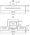
- FIG. 7depicts the magnetoresistive element 200 after step 158 is completed.
- the first protective layer 212resides between the planarization stop layer 214 and the hard bias layer(s) 208 .
- the first protective layer 212includes materials such as at least one of Ru, Ta, Cr, and NiCr.
- the planarization stop layer 214resides between the first protective layer 212 and the second protective layer 216 .
- the second protective layer 216includes at least one of Ta, Ru, Cr and NiCr.
- the second protective layer 216may be at least partially consumed during ion milling in subsequent processing.
- the second protective layer 216has a thickness of at least forty and not more than one hundred and five Angstroms. In another embodiment, the second protective layer thickness is at least fifty and not more than eighty-five Angstroms.
- step 160includes removing a portion of the hard bias layer(s) 206 as well as removing a portion of the capping structure 210 . In one embodiment, this is accomplished through an ion mill.
- FIG. 8depicts the magnetoresistive device 200 after step 160 is performed.
- an aperture 218has been formed in the hard bias layer(s) 208 ′ as well as in the layers 212 ′, 214 ′, and 216 ′ of the hard bias capping structure 210 .
- the aperture 218is shown as above the magnetoresistive element 204 ′.
- the aperturemay simply be in proximity to the magnetoresistive element 204 ′, rather than directly above the magnetoresistive element 204 ′.
- the aperture 218is shown as small and above the magnetoresistive element 204 ′.
- the aperture 218may be larger and/or located at a different position.
- at least a portion of the second protective layer 216 ′is consumed.
- another portion of the hard bias capping structuremay be exposed in step 160 .
- the mask 206is lifted off, via step 162 .
- a planarizationis performed in step 164 .
- the planarizationmay remove any remaining portion of the mask 206 and other residues.
- the planarization performed in step 164may be a CMP.
- the opening of the aperture 218 in step 160 and the planarization in step 164may be considered part of a planarization enhanced lift-off process.
- the planarization stop layer 214 ′is configured to stop or slow the planarization performed in step 164 .
- the planarization stop layer 214 ′is configured for the planarization of step 164 .
- Fabrication of the device 200may be completed, via step 166 .
- the remaining portions 216 ′′ of the second protective layerare generally completely removed.
- the first protective layer 212 ′′may not completely cover the hard bias layers 208 ′′. Instead, some portion of the hard bias layers 208 ′′, particularly close to the magnetoresistive element 204 ′, may be exposed to a subsequent layer. However, in another embodiment, the first protective layer 212 ′′ may completely cover the hard bias layers 208 ′′.
Landscapes
- Engineering & Computer Science (AREA)
- Manufacturing & Machinery (AREA)
- Hall/Mr Elements (AREA)
- Magnetic Heads (AREA)
Abstract
Description
FIG. 1 depicts aconventional method 10 for providing a magnetoresistive element using a conventional undercut bilayer mask. The layers of the magnetoresistive element are provided, viastep 12. Typically,step 12 includes sputter depositing the layers for a spin valve or other analogous giant magnetoresistive (GMR) element. A capping layer for the magnetic element may also be provided, viastep 14. For example, Ta or DLC might be used. A bilayer mask is provided on the device, viastep 16. The bilayer mask has an undercut at the edges of the mask. The magnetic element is defined, viastep 18. Consequently, portions of the layers for the magnetoresistive element exposed by the bilayer mask are removed. Hard bias layers may then be deposited, viastep 20. A lift-off may be performed, viastep 22. The lift-off removes the bilayer mask. A capping layer, such as Ta, and leads may be provided, viastep 24.- Although the
conventional method 10 functions at lower densities, issues arise for higher densities. The bottom layer of the bilayer mask has a smaller width, or critical dimension, than the upper layer. Consequently, as discussed above, the bilayer mask is undercut. However, at smaller critical dimensions on the order of 0.06-0.08 μm or less, significant issues are encountered. In particular, the bilayer mask tends to collapse. In addition, the track width becomes difficult to control. Consequently, yield is reduced. - Accordingly, what is needed is an improved system and method for providing an magnetoresistive device, particularly which may be suitable for higher memory densities.
- The method and system for providing a magnetoresistive device are disclosed. The magnetoresistive device is formed from a plurality of magnetoresistive layer. The method and system include providing a mask. The mask covers a first portion of the magnetoresistive element layers in at least one device area. The magnetoresistive element(s) are defined using the mask. The method and system include depositing hard bias layer(s). The method and system also include providing a hard bias capping structure on the hard bias layer(s). The hard bias capping structure includes a first protective layer and a planarization stop layer. The first protective layer resides between the planarization stop layer and the hard bias layer(s). The method and system also include performing a planarization. The planarization stop layer is configured for the planarization.
FIG. 1 depicts a conventional method for fabricating a magnetoresistive device.FIG. 2 depicts a method for fabricating a magnetoresistive deviceFIG. 3 is a flow chart depicting one exemplary embodiment of a method for fabricating a magnetoresistive device.FIG. 4 is a flow chart depicting another exemplary embodiment of a method for fabricating a magnetoresistive device.FIGS. 5-9 depict an exemplary embodiment of a magnetoresistive device during fabrication using a single layer mask.FIG. 2 depicts a morerecent method 70 for fabricating a magnetoresistive device. For simplicity, step may be omitted or combined. Similarly, different and/or additional steps may be used. The magnetoresistive device being fabricated may be part of a read head. The read head may be part of a merged head that also includes a write head (not shown) and resides on a slider (not shown).- The layers of the magnetoresistive element are provided, via
step 72. Typically,step 72 includes sputter depositing the layers for a spin valve, a tunneling magnetoresistive (TMR) junction, or other analogous giant magnetoresistive (GMR) element. A capping layer may also be provided instep 72. For example, Ta or DLC might be used. A single layer mask is provided on the device, viastep 74. As used herein, a single layer photoresist mask has sides that are not undercut. For some single layer masks, an organic underlayer may be used along with a single layer of photoresist. - The magnetic element is defined, via
step 76.Step 76 may include performing a critical junction ion mill. Thus, the magnetoresistive element has been formed from the magnetoresistive layers. A hard bias layer and a capping layer are typically deposited, viasteps step 82. The lift-off removes at least a portion of the single layer mask. A planarization, such as a chemical mechanical planarization (CMP) is performed, viastep 84. Thus, any remaining portion of the single layer mask may be removed by the CMP. In addition, the top surface of the device being formed is substantially flat. Fabrication of the device may then be completed. - Using the
method 70, a magnetoresistive device may be provided. Further, the use of a bi-layer mask having an undercut may be avoided. Consequently, issues due to collapse of the bi-layer mask may be reduced or eliminated. Magnetoresistive elements for use at higher densities may be provided. For example, a magnetoresistive element having a critical dimension of not more than ninety nanometers might be provided. However, there may be large variations in the CMP performed instep 84. In particular, the hard bias layer may be exposed. As a result, the magnetoresistive device may be subject to failure. Consequently, during mass production, a significant percentage of such magnetic devices may be scrapped. As a result, an improved method for fabricating MR devices is still desired. FIG. 3 is a flow chart depicting one exemplary embodiment of amethod 100 for fabricating an MR device having smaller critical dimensions. Although themethod 100 is described in the context of particular steps and particular magnetoresistive elements, other magnetoresistive elements may be provided and different and/or additional steps may be used. The steps described may also include one or more sub-steps. In addition, although themethod 100 is described in the context of providing single layers, in one embodiment, such a layer may include multiple layers. Themethod 100 is also described in the context of providing a single magnetoresistive element. However, themethod 100 may be used to fabricate multiple magnetoresistive elements at substantially the same time.- The
method 100 commences after the layers for the magnetoresistive element have been provided. In one embodiment, the magnetoresistive element layers cover at least one device area and at least one field area. Thus, in a one embodiment, the magnetoresistive element layers are blanket deposited. The magnetoresistive layers may include, for example, layers for a spin valve or tunneling magnetoresistive element. - A mask that covers the portion of the magnetoresistive element layer(s) from which the magnetic element is to be formed is provided, via
step 102. Step102 may include depositing a layer of photoresist and transferring a pattern to the photoresist layer. The mask covers the magnetoresistive element layers in device area(s) and exposes the magnetoresistive element layers in other area(s). Thus, the mask exposes a portion of the magnetoresistive element layers. In one embodiment, the mask is a single layer mask. Such a mask could include a layer of photoresist as well as an underlayer. However, in one embodiment, there is no undercut for the mask. - The magnetoresistive element is defined using the mask, via
step 104. In one embodiment,step 104 includes performing an ion mill. Because of the configuration of the single layer mask, a portion of the magnetoresistive element layers are preferably removed instep 104. The hard bias layer(s) are deposited, viastep 106. The hard bias layer may be blanket deposited instep 106. In one embodiment,step 106 is performed after the magnetoresistive element has been defined. In one embodiment,step 106 includes depositing seed layers for the hard magnetic materials used in the hard bias materials. Step106 includes providing hard magnetic materials, such as CoPt. In addition, an insulating layer between the seed layers and the magnetic element may be provided. - A hard bias capping structure is provided on the hard bias layer(s), via
step 108. In one embodiment, the hard bias capping structure includes at least a first protective layer and a planarization stop layer. The first protective layer resides between the planarization stop layer and the hard bias layer(s). The first protective layer includes materials such as at least one of Ru, Ta, Cr, and NiCr. In one embodiment, the first protective layer is used to protect the hard bias layer and to provide some material for consumption during subsequent ion milling. In one embodiment, the first protective layer has a thickness of at least twenty and not more than one hundred and five Angstroms. In another embodiment, the first protective layer thickness is at least forty and not more eighty Angstroms. As its name suggests, the planarization stop layer is used as a stop layer for a planarization, described below. In one embodiment, the planarization stop layer is a CMP stop layer. The planarization stop layer may include materials such as at least one of Ru and Rh. In one embodiment, the planarization stop layer has a thickness of at least ten and not more than one hundred twenty Angstroms. In another embodiment, the thickness of the planarization stop layer is at least thirty and not more than seventy Angstroms. - In one embodiment, step108 also includes providing a second protective layer on the planarization stop layer. Thus, the planarization stop layer resides between the first protective layer and the second protective layer. The second protective layer includes at least one of Ta, Ru, Cr and NiCr. The second protective layer may be at least partially consumed during ion milling in subsequent processing. In one embodiment, the second protective layer has a thickness of at least forty and not more than one hundred and five Angstroms. In another embodiment, the second protective layer thickness is at least fifty and not more than eighty-five Angstroms.
- A planarization is performed, via
step 110. The planarization performed instep 110 may be a CMP. In one embodiment, the planarization is performed after the mask has been removed, for example by a lift-off process. Thus, the planarization may be considered part of a planarization enhanced lift-off process. In such a process, an aperture is provided through the hard bias layer(s) to assist in liftoff. This aperture may be formed using ion milling. The second protective layer may be substantially consumed during this ion mill. However, at least part of the planarization stop layer and the first protective layer remain. The planarization stop layer is configured for the planarization ofstep 110. The planarization may remove any remaining portion of the mask and other residues. - Using the
method 100, a magnetic element having a low critical dimension may be provided. For example, the magnetoresistive element may have a critical dimension of ninety nanometers or less, particularly if a single layer mask may be employed. Consequently, the advantages of a single layer mask may be achieved. Because of the configuration of the hard bias capping structure, subsequent processing may not adversely affect the materials in the hard bias layer(s). In particular, ion milling and planarization during lift-off may not expose the hard bias layer(s). Consequently, such layers may remain pristine. As a result, failure of the devices may be reduced or minimized. Fabrication of the magnetoresistive device is thereby enhanced. FIG. 4 is a flow chart depicting another exemplary embodiment of amethod 150 for fabricating an magnetoresistive device.FIGS. 5-9 depict an exemplary embodiment of amagnetoresistive device 200 during fabrication. Referring toFIGS. 4-9 , in one embodiment, the magnetoresistive elements being formed have critical dimensions of not more than ninety nanometers. Although themethod 150 is described in the context of particular steps and particular magnetoresistive elements, one of ordinary skill in the art will recognize that other magnetoresistive elements may be provided and different and/or additional steps may be used. In addition, one of ordinary skill in the art will recognize that the steps described may include one or more sub-steps. In addition, although themethod 150 andmagnetoresistive device 200 are described in the context of providing single layers, such layers may include multiple sub-layers.- The
method 150 commences after the layers for the magnetoresistive element have been provided. The magnetoresistive element layers may cover at least one device area and at least one field area. Thus, in a one embodiment, the magnetoresistive element layers are blanket deposited. The magnetoresistive layers may include, for example, layers for a spin valve, tunneling magnetoresistive element, and/or other GMR structure. - A mask that covers the portion of the magnetoresistive element layer(s) from which the magnetic element is to be formed is provided, via
step 152.FIG. 5 depicts themagnetoresistive device 200 afterstep 152 is performed. Themask 208 covers the magnetoresistive element layers204 in device area(s) and exposes the magnetoresistive element layers in other area(s). Thus, themask 206 exposes a portion of the magnetoresistive device layers204. In the embodiment shown, themask 206 is a single layer mask. Such amask 206 could include a layer of photoresist as well as an underlayer (not shown). However, in one embodiment, there is no undercut for themask 206. Step152 may include depositing a layer of photoresist and transferring a pattern to the photoresist layer. - The magnetoresistive element is defined using the
mask 206, viastep 154. In one embodiment,step 154 includes performing an ion mill. Because of the configuration of themask 154, the exposed portions of the magnetoresistive element layers are removed instep 154. The hard bias layer(s) are deposited, viastep 156. The hard bias layer may be blanket deposited instep 156. In one embodiment,step 156 is performed after the magnetoresistive element has been defined. Step156 includes providing hard magnetic materials, such as CoPt. Seed layers for the hard magnetic materials are also generally provided instep 156.FIG. 6 depicts themagnetoresistive device 200 afterstep 156 is performed. Thus, hadbias layer 208 has been formed. In addition, in one embodiment, step156 may include providing an insulating layer prior to depositing the hard bias layers. Thus, thePMR transducer 200 is shown as including an insulatinglayer 207 and thehard bias layer 208. Thehard bias layer 208 may substantially covers themagnetoresistive device 200. - A hard bias capping structure is provided on the hard bias layer(s), via
step 158. In one embodiment, the hard bias capping structure includes a first protective layer, a planarization stop layer, and a second protective layer. These layer are analogous to these described above.FIG. 7 depicts themagnetoresistive element 200 afterstep 158 is completed. Thus, the firstprotective layer 212, theplanarization stop layer 214, and secondprotective layer 216 are all shown. The firstprotective layer 212 resides between theplanarization stop layer 214 and the hard bias layer(s)208. The firstprotective layer 212 includes materials such as at least one of Ru, Ta, Cr, and NiCr. In one embodiment, the firstprotective layer 212 is used to protect thehard bias layer 208 and to provide some material for consumption during subsequent ion milling. In one embodiment, the firstprotective layer 212 has a thickness of at least twenty and not more than one hundred and five Angstroms. In another embodiment, the first protective layer thickness is at least forty and not more eighty Angstroms. - The
planarization stop layer 214 is used as a stop layer for a planarization, discussed below. In one embodiment, theplanarization stop layer 214 is a CMP stop layer. Theplanarization stop layer 214 may include materials such as at least one of Ru and Rh. In one embodiment, theplanarization stop layer 214 has a thickness of at least ten and not more than one hundred twenty Angstroms. In another embodiment, the thickness of theplanarization stop layer 214 is at least thirty and not more than seventy Angstroms. - The
planarization stop layer 214 resides between the firstprotective layer 212 and the secondprotective layer 216. The secondprotective layer 216 includes at least one of Ta, Ru, Cr and NiCr. The secondprotective layer 216 may be at least partially consumed during ion milling in subsequent processing. In one embodiment, the secondprotective layer 216 has a thickness of at least forty and not more than one hundred and five Angstroms. In another embodiment, the second protective layer thickness is at least fifty and not more than eighty-five Angstroms. - An aperture is provided in the hard bias layer(s)208 in order to assist in lift-off of the
mask 206, viastep 160. In one embodiment,step 160 includes removing a portion of the hard bias layer(s)206 as well as removing a portion of thecapping structure 210. In one embodiment, this is accomplished through an ion mill.FIG. 8 depicts themagnetoresistive device 200 afterstep 160 is performed. Thus, anaperture 218 has been formed in the hard bias layer(s)208′ as well as in thelayers 212′,214′, and216′ of the hardbias capping structure 210. Theaperture 218 is shown as above themagnetoresistive element 204′. In another embodiment, the aperture may simply be in proximity to themagnetoresistive element 204′, rather than directly above themagnetoresistive element 204′. For simplicity, therefore, theaperture 218 is shown as small and above themagnetoresistive element 204′. However, theaperture 218 may be larger and/or located at a different position. During ion milling, at least a portion of the secondprotective layer 216′ is consumed. Thus, another portion of the hard bias capping structure may be exposed instep 160. - The
mask 206 is lifted off, viastep 162. In addition, a planarization is performed instep 164. The planarization may remove any remaining portion of themask 206 and other residues. The planarization performed instep 164 may be a CMP. In one embodiment, the opening of theaperture 218 instep 160 and the planarization instep 164 may be considered part of a planarization enhanced lift-off process. Theplanarization stop layer 214′ is configured to stop or slow the planarization performed instep 164. Thus, theplanarization stop layer 214′ is configured for the planarization ofstep 164. FIG. 9 depicts themagnetoresistive device 200 afterstep 164 has been completed. Thus, themask 206 has been removed and thedevice 200 undergone planarization. Portions of the hardbias capping structure 210″ have been removed. Thus, onlyportions 216″ of the secondprotective layer 216 remain. In one embodiment, theportions 216″ remaining include residues of the second protective layer. Althoughportions 216″ are shown both near and distal from themagnetoresistive element 204′, the portions may be located elsewhere. In addition, one or more of theportions 216″ may not be present at all. Therefore, theportions 216″ near and/or far from themagnetoresistive element 204′ might be present. At least a portion of theplanarization stop layer 214′ has also been removed during the planarization. Consequently, only remainingportions 214″ are shown inFIG. 9 . The remaining portions of theplanarization stop layer 214″ may completely cover the firstplanarization stop layer 212″ as shown on the right side ofFIG. 9 . Alternatively, portions of the firstplanarization stop layer 212″ may be exposed, as is shown on the left side ofFIG. 9 .- Fabrication of the
device 200 may be completed, viastep 166. After fabrication has been completed, the remainingportions 216″ of the second protective layer are generally completely removed. In addition, the firstprotective layer 212″ may not completely cover the hard bias layers208″. Instead, some portion of the hard bias layers208″, particularly close to themagnetoresistive element 204′, may be exposed to a subsequent layer. However, in another embodiment, the firstprotective layer 212″ may completely cover the hard bias layers208″. - Using the
method 150, a magnetic element having a low critical dimension may be provided. For example, the magnetoresistive element may have a critical dimension of ninety nanometers or less, particularly if a single layer mask may be employed. In addition, due to the configuration of the hardbias capping structure 210/210′, subsequent processing may not adversely affect the materials in the hard bias layer(s)208″. In particular, ion milling and planarization during lift-off may not expose the hard bias layer(s)208″. As a result, failure of the devices may be reduced or minimized. Fabrication of themagnetoresistive device 200 may thus be improved.
Claims (19)
Priority Applications (4)
| Application Number | Priority Date | Filing Date | Title |
|---|---|---|---|
| US12/060,724US8316527B2 (en) | 2008-04-01 | 2008-04-01 | Method for providing at least one magnetoresistive device |
| CN200910004719.1ACN101552320B (en) | 2008-04-01 | 2009-02-20 | Method and system for providing a hard bias capping layer |
| HK10100253.0AHK1136086B (en) | 2008-04-01 | 2010-01-11 | Method and system for providing a hard bias capping layer |
| US13/467,354US8614864B1 (en) | 2008-04-01 | 2012-05-09 | Magnetoresistive device with a hard bias capping layer |
Applications Claiming Priority (1)
| Application Number | Priority Date | Filing Date | Title |
|---|---|---|---|
| US12/060,724US8316527B2 (en) | 2008-04-01 | 2008-04-01 | Method for providing at least one magnetoresistive device |
Related Child Applications (1)
| Application Number | Title | Priority Date | Filing Date |
|---|---|---|---|
| US13/467,354DivisionUS8614864B1 (en) | 2008-04-01 | 2012-05-09 | Magnetoresistive device with a hard bias capping layer |
Publications (2)
| Publication Number | Publication Date |
|---|---|
| US20090244789A1true US20090244789A1 (en) | 2009-10-01 |
| US8316527B2 US8316527B2 (en) | 2012-11-27 |
Family
ID=41116845
Family Applications (2)
| Application Number | Title | Priority Date | Filing Date |
|---|---|---|---|
| US12/060,724Expired - Fee RelatedUS8316527B2 (en) | 2008-04-01 | 2008-04-01 | Method for providing at least one magnetoresistive device |
| US13/467,354Expired - Fee RelatedUS8614864B1 (en) | 2008-04-01 | 2012-05-09 | Magnetoresistive device with a hard bias capping layer |
Family Applications After (1)
| Application Number | Title | Priority Date | Filing Date |
|---|---|---|---|
| US13/467,354Expired - Fee RelatedUS8614864B1 (en) | 2008-04-01 | 2012-05-09 | Magnetoresistive device with a hard bias capping layer |
Country Status (2)
| Country | Link |
|---|---|
| US (2) | US8316527B2 (en) |
| CN (1) | CN101552320B (en) |
Cited By (7)
| Publication number | Priority date | Publication date | Assignee | Title |
|---|---|---|---|---|
| US20120156390A1 (en)* | 2010-12-21 | 2012-06-21 | Hitachi Global Storage Technologies Netherlands B.V. | Multi-angle hard bias deposition for optimal hard-bias deposition in a magnetic sensor |
| US8400733B2 (en) | 2010-11-24 | 2013-03-19 | HGST Netherlands B.V. | Process to make PMR writer with leading edge shield (LES) and leading edge taper (LET) |
| US8470186B2 (en) | 2010-11-24 | 2013-06-25 | HGST Netherlands B.V. | Perpendicular write head with wrap around shield and conformal side gap |
| US8524095B2 (en) | 2010-11-24 | 2013-09-03 | HGST Netherlands B.V. | Process to make PMR writer with leading edge shield (LES) and leading edge taper (LET) |
| US8553371B2 (en) | 2010-11-24 | 2013-10-08 | HGST Netherlands B.V. | TMR reader without DLC capping structure |
| WO2019133479A1 (en)* | 2017-12-30 | 2019-07-04 | Spin Memory, Inc. | Method for combining nvm class and sram class mram elements on the same chip |
| US10427689B2 (en) | 2014-11-28 | 2019-10-01 | Denso Corporation | Vehicle control apparatus |
Families Citing this family (135)
| Publication number | Priority date | Publication date | Assignee | Title |
|---|---|---|---|---|
| US8689430B1 (en) | 2006-11-29 | 2014-04-08 | Western Digital (Fremont), Llc | Method for providing a perpendicular magnetic recording (PMR)head |
| US9196270B1 (en) | 2006-12-07 | 2015-11-24 | Western Digital (Fremont), Llc | Method for providing a magnetoresistive element having small critical dimensions |
| US8316527B2 (en) | 2008-04-01 | 2012-11-27 | Western Digital (Fremont), Llc | Method for providing at least one magnetoresistive device |
| US8349195B1 (en) | 2008-06-27 | 2013-01-08 | Western Digital (Fremont), Llc | Method and system for providing a magnetoresistive structure using undercut free mask |
| US8404128B1 (en) | 2009-02-23 | 2013-03-26 | Western Digital (Fremont), Llc | Method and system for providing a perpendicular magnetic recording head |
| US8400731B1 (en) | 2009-04-19 | 2013-03-19 | Western Digital (Fremont), Llc | Write head with variable side shield gaps |
| US8611055B1 (en) | 2009-07-31 | 2013-12-17 | Western Digital (Fremont), Llc | Magnetic etch-stop layer for magnetoresistive read heads |
| US9202480B2 (en) | 2009-10-14 | 2015-12-01 | Western Digital (Fremont), LLC. | Double patterning hard mask for damascene perpendicular magnetic recording (PMR) writer |
| US8441896B2 (en) | 2010-06-25 | 2013-05-14 | Western Digital (Fremont), Llc | Energy assisted magnetic recording head having laser integrated mounted to slider |
| US8997832B1 (en) | 2010-11-23 | 2015-04-07 | Western Digital (Fremont), Llc | Method of fabricating micrometer scale components |
| US8441756B1 (en) | 2010-12-16 | 2013-05-14 | Western Digital (Fremont), Llc | Method and system for providing an antiferromagnetically coupled writer |
| US9123359B1 (en) | 2010-12-22 | 2015-09-01 | Western Digital (Fremont), Llc | Magnetic recording transducer with sputtered antiferromagnetic coupling trilayer between plated ferromagnetic shields and method of fabrication |
| US8456961B1 (en) | 2011-03-22 | 2013-06-04 | Western Digital (Fremont), Llc | Systems and methods for mounting and aligning a laser in an electrically assisted magnetic recording assembly |
| US8419954B1 (en) | 2011-10-31 | 2013-04-16 | Western Digital (Fremont), Llc | Method for providing a side shield for a magnetic recording transducer |
| US8451563B1 (en) | 2011-12-20 | 2013-05-28 | Western Digital (Fremont), Llc | Method for providing a side shield for a magnetic recording transducer using an air bridge |
| US8760823B1 (en) | 2011-12-20 | 2014-06-24 | Western Digital (Fremont), Llc | Method and system for providing a read transducer having soft and hard magnetic bias structures |
| US9093639B2 (en) | 2012-02-21 | 2015-07-28 | Western Digital (Fremont), Llc | Methods for manufacturing a magnetoresistive structure utilizing heating and cooling |
| US9349392B1 (en) | 2012-05-24 | 2016-05-24 | Western Digital (Fremont), Llc | Methods for improving adhesion on dielectric substrates |
| US8724259B1 (en) | 2012-06-11 | 2014-05-13 | Western Digital (Fremont), Llc | Conformal high moment side shield seed layer for perpendicular magnetic recording writer |
| US8711528B1 (en) | 2012-06-29 | 2014-04-29 | Western Digital (Fremont), Llc | Tunnel magnetoresistance read head with narrow shield-to-shield spacing |
| US9269382B1 (en) | 2012-06-29 | 2016-02-23 | Western Digital (Fremont), Llc | Method and system for providing a read transducer having improved pinning of the pinned layer at higher recording densities |
| KR101998676B1 (en)* | 2012-07-20 | 2019-07-10 | 삼성전자주식회사 | Magnetic Memory Device and Method of fabricating the same |
| US9213322B1 (en) | 2012-08-16 | 2015-12-15 | Western Digital (Fremont), Llc | Methods for providing run to run process control using a dynamic tuner |
| US8984740B1 (en) | 2012-11-30 | 2015-03-24 | Western Digital (Fremont), Llc | Process for providing a magnetic recording transducer having a smooth magnetic seed layer |
| US9053719B2 (en) | 2012-11-30 | 2015-06-09 | Western Digital (Fremont), Llc | Magnetoresistive sensor for a magnetic storage system read head, and fabrication method thereof |
| US8980109B1 (en) | 2012-12-11 | 2015-03-17 | Western Digital (Fremont), Llc | Method for providing a magnetic recording transducer using a combined main pole and side shield CMP for a wraparound shield scheme |
| US8760818B1 (en) | 2013-01-09 | 2014-06-24 | Western Digital (Fremont), Llc | Systems and methods for providing magnetic storage elements with high magneto-resistance using heusler alloys |
| US9042208B1 (en) | 2013-03-11 | 2015-05-26 | Western Digital Technologies, Inc. | Disk drive measuring fly height by applying a bias voltage to an electrically insulated write component of a head |
| US8883017B1 (en) | 2013-03-12 | 2014-11-11 | Western Digital (Fremont), Llc | Method and system for providing a read transducer having seamless interfaces |
| US8947834B2 (en)* | 2013-03-12 | 2015-02-03 | Seagate Technology Llc | Method and apparatus for chemical-mechanical polishing |
| US9336814B1 (en) | 2013-03-12 | 2016-05-10 | Western Digital (Fremont), Llc | Inverse tapered waveguide for use in a heat assisted magnetic recording head |
| US9111564B1 (en) | 2013-04-02 | 2015-08-18 | Western Digital (Fremont), Llc | Magnetic recording writer having a main pole with multiple flare angles |
| US9013836B1 (en) | 2013-04-02 | 2015-04-21 | Western Digital (Fremont), Llc | Method and system for providing an antiferromagnetically coupled return pole |
| US9104107B1 (en) | 2013-04-03 | 2015-08-11 | Western Digital (Fremont), Llc | DUV photoresist process |
| US8993217B1 (en) | 2013-04-04 | 2015-03-31 | Western Digital (Fremont), Llc | Double exposure technique for high resolution disk imaging |
| US9070381B1 (en) | 2013-04-12 | 2015-06-30 | Western Digital (Fremont), Llc | Magnetic recording read transducer having a laminated free layer |
| US9245545B1 (en) | 2013-04-12 | 2016-01-26 | Wester Digital (Fremont), Llc | Short yoke length coils for magnetic heads in disk drives |
| US9064527B1 (en) | 2013-04-12 | 2015-06-23 | Western Digital (Fremont), Llc | High order tapered waveguide for use in a heat assisted magnetic recording head |
| US9431047B1 (en) | 2013-05-01 | 2016-08-30 | Western Digital (Fremont), Llc | Method for providing an improved AFM reader shield |
| US9064528B1 (en) | 2013-05-17 | 2015-06-23 | Western Digital Technologies, Inc. | Interferometric waveguide usable in shingled heat assisted magnetic recording in the absence of a near-field transducer |
| US9431039B1 (en) | 2013-05-21 | 2016-08-30 | Western Digital (Fremont), Llc | Multiple sensor array usable in two-dimensional magnetic recording |
| US9263067B1 (en) | 2013-05-29 | 2016-02-16 | Western Digital (Fremont), Llc | Process for making PMR writer with constant side wall angle |
| US9361913B1 (en) | 2013-06-03 | 2016-06-07 | Western Digital (Fremont), Llc | Recording read heads with a multi-layer AFM layer methods and apparatuses |
| US9406331B1 (en) | 2013-06-17 | 2016-08-02 | Western Digital (Fremont), Llc | Method for making ultra-narrow read sensor and read transducer device resulting therefrom |
| US9287494B1 (en) | 2013-06-28 | 2016-03-15 | Western Digital (Fremont), Llc | Magnetic tunnel junction (MTJ) with a magnesium oxide tunnel barrier |
| US9318130B1 (en) | 2013-07-02 | 2016-04-19 | Western Digital (Fremont), Llc | Method to fabricate tunneling magnetic recording heads with extended pinned layer |
| US8947985B1 (en) | 2013-07-16 | 2015-02-03 | Western Digital (Fremont), Llc | Heat assisted magnetic recording transducers having a recessed pole |
| US8923102B1 (en) | 2013-07-16 | 2014-12-30 | Western Digital (Fremont), Llc | Optical grating coupling for interferometric waveguides in heat assisted magnetic recording heads |
| US9431032B1 (en) | 2013-08-14 | 2016-08-30 | Western Digital (Fremont), Llc | Electrical connection arrangement for a multiple sensor array usable in two-dimensional magnetic recording |
| US9275657B1 (en) | 2013-08-14 | 2016-03-01 | Western Digital (Fremont), Llc | Process for making PMR writer with non-conformal side gaps |
| US9042051B2 (en) | 2013-08-15 | 2015-05-26 | Western Digital (Fremont), Llc | Gradient write gap for perpendicular magnetic recording writer |
| US9343098B1 (en) | 2013-08-23 | 2016-05-17 | Western Digital (Fremont), Llc | Method for providing a heat assisted magnetic recording transducer having protective pads |
| US9343086B1 (en) | 2013-09-11 | 2016-05-17 | Western Digital (Fremont), Llc | Magnetic recording write transducer having an improved sidewall angle profile |
| US9441938B1 (en) | 2013-10-08 | 2016-09-13 | Western Digital (Fremont), Llc | Test structures for measuring near field transducer disc length |
| US9042058B1 (en) | 2013-10-17 | 2015-05-26 | Western Digital Technologies, Inc. | Shield designed for middle shields in a multiple sensor array |
| US9349394B1 (en) | 2013-10-18 | 2016-05-24 | Western Digital (Fremont), Llc | Method for fabricating a magnetic writer having a gradient side gap |
| US9007719B1 (en) | 2013-10-23 | 2015-04-14 | Western Digital (Fremont), Llc | Systems and methods for using double mask techniques to achieve very small features |
| US9214172B2 (en) | 2013-10-23 | 2015-12-15 | Western Digital (Fremont), Llc | Method of manufacturing a magnetic read head |
| US8988812B1 (en) | 2013-11-27 | 2015-03-24 | Western Digital (Fremont), Llc | Multi-sensor array configuration for a two-dimensional magnetic recording (TDMR) operation |
| US9194692B1 (en) | 2013-12-06 | 2015-11-24 | Western Digital (Fremont), Llc | Systems and methods for using white light interferometry to measure undercut of a bi-layer structure |
| US9280990B1 (en) | 2013-12-11 | 2016-03-08 | Western Digital (Fremont), Llc | Method for fabricating a magnetic writer using multiple etches |
| US9001628B1 (en) | 2013-12-16 | 2015-04-07 | Western Digital (Fremont), Llc | Assistant waveguides for evaluating main waveguide coupling efficiency and diode laser alignment tolerances for hard disk |
| US9082423B1 (en) | 2013-12-18 | 2015-07-14 | Western Digital (Fremont), Llc | Magnetic recording write transducer having an improved trailing surface profile |
| US8917581B1 (en) | 2013-12-18 | 2014-12-23 | Western Digital Technologies, Inc. | Self-anneal process for a near field transducer and chimney in a hard disk drive assembly |
| US9147408B1 (en) | 2013-12-19 | 2015-09-29 | Western Digital (Fremont), Llc | Heated AFM layer deposition and cooling process for TMR magnetic recording sensor with high pinning field |
| US8971160B1 (en) | 2013-12-19 | 2015-03-03 | Western Digital (Fremont), Llc | Near field transducer with high refractive index pin for heat assisted magnetic recording |
| US8970988B1 (en) | 2013-12-31 | 2015-03-03 | Western Digital (Fremont), Llc | Electric gaps and method for making electric gaps for multiple sensor arrays |
| US9305583B1 (en) | 2014-02-18 | 2016-04-05 | Western Digital (Fremont), Llc | Method for fabricating a magnetic writer using multiple etches of damascene materials |
| US9183854B2 (en) | 2014-02-24 | 2015-11-10 | Western Digital (Fremont), Llc | Method to make interferometric taper waveguide for HAMR light delivery |
| US8988825B1 (en) | 2014-02-28 | 2015-03-24 | Western Digital (Fremont, LLC | Method for fabricating a magnetic writer having half-side shields |
| US9142233B1 (en) | 2014-02-28 | 2015-09-22 | Western Digital (Fremont), Llc | Heat assisted magnetic recording writer having a recessed pole |
| US9396743B1 (en) | 2014-02-28 | 2016-07-19 | Western Digital (Fremont), Llc | Systems and methods for controlling soft bias thickness for tunnel magnetoresistance readers |
| US9202493B1 (en) | 2014-02-28 | 2015-12-01 | Western Digital (Fremont), Llc | Method of making an ultra-sharp tip mode converter for a HAMR head |
| US9001467B1 (en) | 2014-03-05 | 2015-04-07 | Western Digital (Fremont), Llc | Method for fabricating side shields in a magnetic writer |
| US9153255B1 (en) | 2014-03-05 | 2015-10-06 | Western Digital (Fremont), Llc | Method for fabricating a magnetic writer having an asymmetric gap and shields |
| US9135930B1 (en) | 2014-03-06 | 2015-09-15 | Western Digital (Fremont), Llc | Method for fabricating a magnetic write pole using vacuum deposition |
| US9934811B1 (en) | 2014-03-07 | 2018-04-03 | Western Digital (Fremont), Llc | Methods for controlling stray fields of magnetic features using magneto-elastic anisotropy |
| US9190085B1 (en) | 2014-03-12 | 2015-11-17 | Western Digital (Fremont), Llc | Waveguide with reflective grating for localized energy intensity |
| US9111558B1 (en) | 2014-03-14 | 2015-08-18 | Western Digital (Fremont), Llc | System and method of diffractive focusing of light in a waveguide |
| US9135937B1 (en) | 2014-05-09 | 2015-09-15 | Western Digital (Fremont), Llc | Current modulation on laser diode for energy assisted magnetic recording transducer |
| US9007879B1 (en) | 2014-06-10 | 2015-04-14 | Western Digital (Fremont), Llc | Interfering near field transducer having a wide metal bar feature for energy assisted magnetic recording |
| US8958272B1 (en) | 2014-06-10 | 2015-02-17 | Western Digital (Fremont), Llc | Interfering near field transducer for energy assisted magnetic recording |
| US8976635B1 (en) | 2014-06-10 | 2015-03-10 | Western Digital (Fremont), Llc | Near field transducer driven by a transverse electric waveguide for energy assisted magnetic recording |
| US8953422B1 (en) | 2014-06-10 | 2015-02-10 | Western Digital (Fremont), Llc | Near field transducer using dielectric waveguide core with fine ridge feature |
| US9508363B1 (en) | 2014-06-17 | 2016-11-29 | Western Digital (Fremont), Llc | Method for fabricating a magnetic write pole having a leading edge bevel |
| US9361914B1 (en) | 2014-06-18 | 2016-06-07 | Western Digital (Fremont), Llc | Magnetic sensor with thin capping layer |
| US9214169B1 (en) | 2014-06-20 | 2015-12-15 | Western Digital (Fremont), Llc | Magnetic recording read transducer having a laminated free layer |
| US9053735B1 (en) | 2014-06-20 | 2015-06-09 | Western Digital (Fremont), Llc | Method for fabricating a magnetic writer using a full-film metal planarization |
| US9042052B1 (en) | 2014-06-23 | 2015-05-26 | Western Digital (Fremont), Llc | Magnetic writer having a partially shunted coil |
| US9230565B1 (en) | 2014-06-24 | 2016-01-05 | Western Digital (Fremont), Llc | Magnetic shield for magnetic recording head |
| US9190079B1 (en) | 2014-09-22 | 2015-11-17 | Western Digital (Fremont), Llc | Magnetic write pole having engineered radius of curvature and chisel angle profiles |
| US9007725B1 (en) | 2014-10-07 | 2015-04-14 | Western Digital (Fremont), Llc | Sensor with positive coupling between dual ferromagnetic free layer laminates |
| US9087527B1 (en) | 2014-10-28 | 2015-07-21 | Western Digital (Fremont), Llc | Apparatus and method for middle shield connection in magnetic recording transducers |
| US9786301B1 (en) | 2014-12-02 | 2017-10-10 | Western Digital (Fremont), Llc | Apparatuses and methods for providing thin shields in a multiple sensor array |
| US9721595B1 (en) | 2014-12-04 | 2017-08-01 | Western Digital (Fremont), Llc | Method for providing a storage device |
| US9111550B1 (en) | 2014-12-04 | 2015-08-18 | Western Digital (Fremont), Llc | Write transducer having a magnetic buffer layer spaced between a side shield and a write pole by non-magnetic layers |
| US9236560B1 (en) | 2014-12-08 | 2016-01-12 | Western Digital (Fremont), Llc | Spin transfer torque tunneling magnetoresistive device having a laminated free layer with perpendicular magnetic anisotropy |
| US9286919B1 (en) | 2014-12-17 | 2016-03-15 | Western Digital (Fremont), Llc | Magnetic writer having a dual side gap |
| US9881638B1 (en) | 2014-12-17 | 2018-01-30 | Western Digital (Fremont), Llc | Method for providing a near-field transducer (NFT) for a heat assisted magnetic recording (HAMR) device |
| US9214165B1 (en) | 2014-12-18 | 2015-12-15 | Western Digital (Fremont), Llc | Magnetic writer having a gradient in saturation magnetization of the shields |
| US9741366B1 (en) | 2014-12-18 | 2017-08-22 | Western Digital (Fremont), Llc | Method for fabricating a magnetic writer having a gradient in saturation magnetization of the shields |
| US10074387B1 (en) | 2014-12-21 | 2018-09-11 | Western Digital (Fremont), Llc | Method and system for providing a read transducer having symmetric antiferromagnetically coupled shields |
| US9343087B1 (en) | 2014-12-21 | 2016-05-17 | Western Digital (Fremont), Llc | Method for fabricating a magnetic writer having half shields |
| US9437251B1 (en) | 2014-12-22 | 2016-09-06 | Western Digital (Fremont), Llc | Apparatus and method having TDMR reader to reader shunts |
| US9449625B1 (en) | 2014-12-24 | 2016-09-20 | Western Digital (Fremont), Llc | Heat assisted magnetic recording head having a plurality of diffusion barrier layers |
| US9123374B1 (en) | 2015-02-12 | 2015-09-01 | Western Digital (Fremont), Llc | Heat assisted magnetic recording writer having an integrated polarization rotation plate |
| US9312064B1 (en) | 2015-03-02 | 2016-04-12 | Western Digital (Fremont), Llc | Method to fabricate a magnetic head including ion milling of read gap using dual layer hard mask |
| US9443541B1 (en) | 2015-03-24 | 2016-09-13 | Western Digital (Fremont), Llc | Magnetic writer having a gradient in saturation magnetization of the shields and return pole |
| US9431031B1 (en) | 2015-03-24 | 2016-08-30 | Western Digital (Fremont), Llc | System and method for magnetic transducers having multiple sensors and AFC shields |
| US9449621B1 (en) | 2015-03-26 | 2016-09-20 | Western Digital (Fremont), Llc | Dual free layer magnetic reader having a rear bias structure having a high aspect ratio |
| US9384763B1 (en) | 2015-03-26 | 2016-07-05 | Western Digital (Fremont), Llc | Dual free layer magnetic reader having a rear bias structure including a soft bias layer |
| US9245562B1 (en) | 2015-03-30 | 2016-01-26 | Western Digital (Fremont), Llc | Magnetic recording writer with a composite main pole |
| US9263071B1 (en) | 2015-03-31 | 2016-02-16 | Western Digital (Fremont), Llc | Flat NFT for heat assisted magnetic recording |
| US9147404B1 (en) | 2015-03-31 | 2015-09-29 | Western Digital (Fremont), Llc | Method and system for providing a read transducer having a dual free layer |
| US9508372B1 (en) | 2015-06-03 | 2016-11-29 | Western Digital (Fremont), Llc | Shingle magnetic writer having a low sidewall angle pole |
| US9508365B1 (en) | 2015-06-24 | 2016-11-29 | Western Digital (Fremont), LLC. | Magnetic reader having a crystal decoupling structure |
| US9530443B1 (en) | 2015-06-25 | 2016-12-27 | Western Digital (Fremont), Llc | Method for fabricating a magnetic recording device having a high aspect ratio structure |
| US9646639B2 (en) | 2015-06-26 | 2017-05-09 | Western Digital (Fremont), Llc | Heat assisted magnetic recording writer having integrated polarization rotation waveguides |
| US9842615B1 (en) | 2015-06-26 | 2017-12-12 | Western Digital (Fremont), Llc | Magnetic reader having a nonmagnetic insertion layer for the pinning layer |
| US9431038B1 (en) | 2015-06-29 | 2016-08-30 | Western Digital (Fremont), Llc | Method for fabricating a magnetic write pole having an improved sidewall angle profile |
| US9666214B1 (en) | 2015-09-23 | 2017-05-30 | Western Digital (Fremont), Llc | Free layer magnetic reader that may have a reduced shield-to-shield spacing |
| US9472216B1 (en) | 2015-09-23 | 2016-10-18 | Western Digital (Fremont), Llc | Differential dual free layer magnetic reader |
| US9384765B1 (en) | 2015-09-24 | 2016-07-05 | Western Digital (Fremont), Llc | Method and system for providing a HAMR writer having improved optical efficiency |
| US9424866B1 (en) | 2015-09-24 | 2016-08-23 | Western Digital (Fremont), Llc | Heat assisted magnetic recording write apparatus having a dielectric gap |
| US9595273B1 (en) | 2015-09-30 | 2017-03-14 | Western Digital (Fremont), Llc | Shingle magnetic writer having nonconformal shields |
| US9484051B1 (en) | 2015-11-09 | 2016-11-01 | The Provost, Fellows, Foundation Scholars and the other members of Board, of the College of the Holy and Undivided Trinity of Queen Elizabeth near Dublin | Method and system for reducing undesirable reflections in a HAMR write apparatus |
| US9953670B1 (en) | 2015-11-10 | 2018-04-24 | Western Digital (Fremont), Llc | Method and system for providing a HAMR writer including a multi-mode interference device |
| US10037770B1 (en) | 2015-11-12 | 2018-07-31 | Western Digital (Fremont), Llc | Method for providing a magnetic recording write apparatus having a seamless pole |
| US9812155B1 (en) | 2015-11-23 | 2017-11-07 | Western Digital (Fremont), Llc | Method and system for fabricating high junction angle read sensors |
| US9564150B1 (en) | 2015-11-24 | 2017-02-07 | Western Digital (Fremont), Llc | Magnetic read apparatus having an improved read sensor isolation circuit |
| US9799351B1 (en) | 2015-11-30 | 2017-10-24 | Western Digital (Fremont), Llc | Short yoke length writer having assist coils |
| US9754611B1 (en) | 2015-11-30 | 2017-09-05 | Western Digital (Fremont), Llc | Magnetic recording write apparatus having a stepped conformal trailing shield |
| US9767831B1 (en) | 2015-12-01 | 2017-09-19 | Western Digital (Fremont), Llc | Magnetic writer having convex trailing surface pole and conformal write gap |
| US9740805B1 (en) | 2015-12-01 | 2017-08-22 | Western Digital (Fremont), Llc | Method and system for detecting hotspots for photolithographically-defined devices |
| US9858951B1 (en) | 2015-12-01 | 2018-01-02 | Western Digital (Fremont), Llc | Method for providing a multilayer AFM layer in a read sensor |
Citations (45)
| Publication number | Priority date | Publication date | Assignee | Title |
|---|---|---|---|---|
| US4939837A (en)* | 1988-09-01 | 1990-07-10 | International Business Machines Corporation | Batch fabrication process for magnetic heads |
| US5654128A (en)* | 1994-10-21 | 1997-08-05 | Ngk Insulators, Ltd. | Single resist layer lift-off process for forming patterned layers on a substrate |
| US5669133A (en)* | 1992-08-25 | 1997-09-23 | Seagate Technology, Inc. | Method of making a magnetoresistive sensor |
| US5718976A (en)* | 1991-05-03 | 1998-02-17 | Advanced Refractory Technologies, Inc. | Erosion resistant diamond-like nanocomposite coatings for optical components |
| US6156485A (en)* | 1999-01-19 | 2000-12-05 | Taiwan Semiconductor Manufacturing Company Ltd. | Film scheme to solve high aspect ratio metal etch masking layer selectivity and improve photo I-line PR resolution capability in quarter-micron technology |
| US6211061B1 (en)* | 1999-10-29 | 2001-04-03 | Taiwan Semiconductor Manufactuirng Company | Dual damascene process for carbon-based low-K materials |
| US6212047B1 (en)* | 1989-11-27 | 2001-04-03 | Censtor Corporation | Hard disk drive with magnetoresistive head and perpendicular media |
| US6309955B1 (en)* | 2001-02-16 | 2001-10-30 | Advanced Micro Devices, Inc. | Method for using a CVD organic barc as a hard mask during via etch |
| US6421212B1 (en)* | 1999-09-21 | 2002-07-16 | Read-Rite Corporation | Thin film read head structure with improved bias magnet-to-magnetoresistive element interface and method of fabrication |
| US6468642B1 (en)* | 1995-10-03 | 2002-10-22 | N.V. Bekaert S.A. | Fluorine-doped diamond-like coatings |
| US6495311B1 (en)* | 2000-03-17 | 2002-12-17 | International Business Machines Corporation | Bilayer liftoff process for high moment laminate |
| US6493926B2 (en)* | 2001-04-16 | 2002-12-17 | Headway Technologies, Inc. | Bi-layer lift-off process for high track density GMR head |
| US6496334B1 (en)* | 2000-05-26 | 2002-12-17 | Read-Rite Corportion | Data storage and retrieval apparatus with thin film read head having planarized extra gap and shield layers and method of fabrication thereof |
| US20030092281A1 (en)* | 2001-11-13 | 2003-05-15 | Chartered Semiconductors Manufactured Limited | Method for organic barc and photoresist trimming process |
| US6582889B1 (en)* | 1999-08-26 | 2003-06-24 | Tdk Corporation | Method for forming resist pattern and manufacturing method of thin-film element |
| US20030179497A1 (en)* | 2002-03-19 | 2003-09-25 | Harris Tom King | Magnetic head having a bilayer pole tip and method of making the same |
| US6632707B1 (en)* | 2001-01-31 | 2003-10-14 | Advanced Micro Devices, Inc. | Method for forming an interconnect structure using a CVD organic BARC to mitigate via poisoning |
| US6713237B2 (en)* | 2000-07-27 | 2004-03-30 | Seagate Technology Llc | Single layer lift-off method for making an electronic device |
| US6728055B1 (en)* | 2000-03-21 | 2004-04-27 | International Business Machines Corporation | Method and apparatus for performing spin valve combined pinned layer reset and hard bias initialization at the HGA level |
| US6798620B2 (en)* | 2000-11-15 | 2004-09-28 | Matsushita Electric Industrial Co., Ltd. | Magneto-resistive element, magnetic head, and magnetic recording and reproduction apparatus |
| US6801408B1 (en)* | 2000-11-02 | 2004-10-05 | Western Digital (Fremont), Inc. | Data storage and retrieval apparatus with thin film read head having a planar sensor element and an extra gap and method of fabrication thereof |
| US20050024793A1 (en)* | 2003-07-29 | 2005-02-03 | Alps Electric Co., Ltd. | Exchange-coupled film, method for making exchange-coupled film, and magnetic sensing element including exchange-coupled film |
| US20050219771A1 (en)* | 2004-03-30 | 2005-10-06 | Rie Sato | Magnetic sensor, magnetic field sensing method, semagnetic recording head, and magnetic memory device |
| US20050227482A1 (en)* | 2004-03-24 | 2005-10-13 | Korzenski Michael B | Composition useful for removal of bottom anti-reflection coatings from patterned ion-implanted photoresist wafers |
| US6989971B2 (en)* | 2002-04-05 | 2006-01-24 | Hitachi Global Storage Technologies Netherlands, B.V. | Giant magnetoresistance (GMR) read head with reactive-ion-etch defined read width and fabrication process |
| US20060025053A1 (en)* | 2004-07-30 | 2006-02-02 | Marie-Claire Cyrille | Method for fabricating a magnetic transducer using a slurry with spherical particles for CMP-assisted photoresist lift-off |
| US20060044705A1 (en)* | 2004-09-01 | 2006-03-02 | Alps Electric Co., Ltd. | CPP magnetic detecting element including a CoFe pinned layer or free layer |
| US7037847B2 (en)* | 2004-05-28 | 2006-05-02 | Hitachi Global Storage Technologies Netherlands, B.V. | Methods for fabricating read sensor for magnetic heads with reduced read track width |
| US7061728B2 (en)* | 2003-07-29 | 2006-06-13 | Hitachi Global Storage Technologies Netherlands B.V. | High linear density read head with a contiguous junction and minimal shield shorts |
| US7070697B2 (en)* | 2003-04-14 | 2006-07-04 | Hitachi Global Storage Technologies Netherlands B.V. | Methods of making a read sensor with use of a barrier structure for depositing materials |
| US20060198059A1 (en)* | 2005-03-04 | 2006-09-07 | Headway Technologies, Inc. | Novel abutted exchange bias design for sensor stabilization |
| US20060196039A1 (en)* | 2005-03-04 | 2006-09-07 | Headway Technologies, Inc. | Novel abutted exchange bias design for sensor stabilization |
| US7146711B2 (en)* | 2002-12-13 | 2006-12-12 | Headway Technologies, Inc. | Method to make planarized GMR head for high track density |
| US20060293208A1 (en)* | 2005-06-23 | 2006-12-28 | Egbe Matthew I | Composition for removal of residue comprising cationic salts and methods using same |
| US7163751B2 (en)* | 2001-09-26 | 2007-01-16 | Shipley Company, L.L.C. | Coating compositions for use with an overcoated photoresist |
| US7175944B2 (en)* | 2004-08-31 | 2007-02-13 | Micron Technology, Inc. | Prevention of photoresist scumming |
| US20070048624A1 (en)* | 2005-08-24 | 2007-03-01 | Chen Tsung Y | Magnetic recording head wiht overlaid leads |
| US7194797B2 (en)* | 2004-06-30 | 2007-03-27 | Hitachi Global Storage Technologies Netherlands B.V. | Method for use in forming a read sensor for a magnetic head |
| US7237321B2 (en)* | 2004-07-30 | 2007-07-03 | Hitachi Global Storage Technologies Netherlands B.V. | Method for fabricating a CPP magnetic transducer using CMP-assisted lift-off and a CMP-resistant metal layer |
| US7262138B1 (en)* | 2004-10-01 | 2007-08-28 | Advanced Micro Devices, Inc. | Organic BARC with adjustable etch rate |
| US7272080B2 (en)* | 2003-06-10 | 2007-09-18 | Canon Kabushiki Kaisha | Recording apparatus |
| US20070217088A1 (en)* | 2003-11-12 | 2007-09-20 | Freitag James M | Method and apparatus for providing magnetostriction control in a freelayer of a magnetic memory device |
| US20070218679A1 (en)* | 2006-03-20 | 2007-09-20 | Applied Materials, Inc. | Organic BARC etch process capable of use in the formation of low k dual damascene integrated circuits |
| US7369371B2 (en)* | 2005-08-15 | 2008-05-06 | Hitachi Global Storage Technologies Netherlands B.V. | Magnetoresistive sensor having a shape enhanced pinned layer |
| US7640650B2 (en)* | 2007-12-28 | 2010-01-05 | Hitachi Global Storage Technologies Netherlands B.V. | Method of making a magnetoresistive reader structure |
Family Cites Families (13)
| Publication number | Priority date | Publication date | Assignee | Title |
|---|---|---|---|---|
| WO1999016057A1 (en)* | 1997-09-22 | 1999-04-01 | Seagate Technology, Inc. | Overlaid mr structure with magnetostatic stabilized soft adjacent layer |
| JP3260740B1 (en)* | 2001-04-25 | 2002-02-25 | ティーディーケイ株式会社 | Method of manufacturing magnetoresistive device and method of manufacturing thin-film magnetic head |
| US6888706B2 (en)* | 2001-08-08 | 2005-05-03 | Alps Electric Co., Ltd. | Magnetic sensing element having hard bias layer formed on bias underlayer and process for manufacturing the same |
| US6785954B2 (en)* | 2002-04-17 | 2004-09-07 | Headway Technologies, Inc. | Method for fabricating lead overlay (LOL) on the bottom spin valve GMR read sensor |
| JP2004152334A (en)* | 2002-10-29 | 2004-05-27 | Hitachi Ltd | Magnetic sensor, method of manufacturing the same, and magnetic recording / reproducing apparatus equipped with the same |
| US7330339B2 (en)* | 2003-07-25 | 2008-02-12 | Hitachi Global Storage Technologies Netherlands B.V. | Structure providing enhanced self-pinning for CPP GMR and tunnel valve heads |
| US7218488B2 (en)* | 2004-03-29 | 2007-05-15 | Hitachi Global Storage Technologies Netherlands B.V. | Method and apparatus for reducing the thickness of a sensor stack in a current-perpendicular-to-plane GMR/tunnel valve sensor |
| US7804668B2 (en)* | 2006-11-16 | 2010-09-28 | Headway Technologies, Inc. | Enhanced hard bias in thin film magnetoresistive sensors with perpendicular easy axis growth of hard bias and strong shield-hard bias coupling |
| US8316527B2 (en) | 2008-04-01 | 2012-11-27 | Western Digital (Fremont), Llc | Method for providing at least one magnetoresistive device |
| US8208230B2 (en)* | 2008-04-10 | 2012-06-26 | Headway Technologies, Inc. | Binary output reader structure (BORS) with high utilization rate |
| US8349195B1 (en) | 2008-06-27 | 2013-01-08 | Western Digital (Fremont), Llc | Method and system for providing a magnetoresistive structure using undercut free mask |
| US8011084B2 (en)* | 2008-07-31 | 2011-09-06 | Hitachi Global Storage Technologies Netherlands B.V. | Method for fabricating narrow magnetic read width TMR/CPP sensors |
| US8296930B2 (en)* | 2009-12-22 | 2012-10-30 | Hitachi Global Storage Technologies Netherlands B.V. | Method for manufacturing a magnetoresistive sensor having a flat shield |
- 2008
- 2008-04-01USUS12/060,724patent/US8316527B2/ennot_activeExpired - Fee Related
- 2009
- 2009-02-20CNCN200910004719.1Apatent/CN101552320B/ennot_activeExpired - Fee Related
- 2012
- 2012-05-09USUS13/467,354patent/US8614864B1/ennot_activeExpired - Fee Related
Patent Citations (54)
| Publication number | Priority date | Publication date | Assignee | Title |
|---|---|---|---|---|
| US4939837A (en)* | 1988-09-01 | 1990-07-10 | International Business Machines Corporation | Batch fabrication process for magnetic heads |
| US6320725B1 (en)* | 1989-11-27 | 2001-11-20 | Censtor Corporation | Hard disk drive having ring head with predominantly perpendicular media fields |
| US6212047B1 (en)* | 1989-11-27 | 2001-04-03 | Censtor Corporation | Hard disk drive with magnetoresistive head and perpendicular media |
| US5718976A (en)* | 1991-05-03 | 1998-02-17 | Advanced Refractory Technologies, Inc. | Erosion resistant diamond-like nanocomposite coatings for optical components |
| US5669133A (en)* | 1992-08-25 | 1997-09-23 | Seagate Technology, Inc. | Method of making a magnetoresistive sensor |
| US5654128A (en)* | 1994-10-21 | 1997-08-05 | Ngk Insulators, Ltd. | Single resist layer lift-off process for forming patterned layers on a substrate |
| US6468642B1 (en)* | 1995-10-03 | 2002-10-22 | N.V. Bekaert S.A. | Fluorine-doped diamond-like coatings |
| US20050094315A1 (en)* | 1995-12-22 | 2005-05-05 | Seagate Technology Llc, A Delaware Corporation | Hard disk drive for perpendicular recording with transducer having submicron gap between pole tips |
| US20020093761A1 (en)* | 1995-12-22 | 2002-07-18 | Payne Alexander P. | Hard disk drive for perpendicular recording with transducer having submicron gap between pole tips |
| US7095585B2 (en)* | 1995-12-22 | 2006-08-22 | Seagate Technology Llc | Hard disk drive for perpendicular recording with transducer having submicron gap between pole tips |
| US6156485A (en)* | 1999-01-19 | 2000-12-05 | Taiwan Semiconductor Manufacturing Company Ltd. | Film scheme to solve high aspect ratio metal etch masking layer selectivity and improve photo I-line PR resolution capability in quarter-micron technology |
| US6582889B1 (en)* | 1999-08-26 | 2003-06-24 | Tdk Corporation | Method for forming resist pattern and manufacturing method of thin-film element |
| US6421212B1 (en)* | 1999-09-21 | 2002-07-16 | Read-Rite Corporation | Thin film read head structure with improved bias magnet-to-magnetoresistive element interface and method of fabrication |
| US6211061B1 (en)* | 1999-10-29 | 2001-04-03 | Taiwan Semiconductor Manufactuirng Company | Dual damascene process for carbon-based low-K materials |
| US6495311B1 (en)* | 2000-03-17 | 2002-12-17 | International Business Machines Corporation | Bilayer liftoff process for high moment laminate |
| US6728055B1 (en)* | 2000-03-21 | 2004-04-27 | International Business Machines Corporation | Method and apparatus for performing spin valve combined pinned layer reset and hard bias initialization at the HGA level |
| US6496334B1 (en)* | 2000-05-26 | 2002-12-17 | Read-Rite Corportion | Data storage and retrieval apparatus with thin film read head having planarized extra gap and shield layers and method of fabrication thereof |
| US6713237B2 (en)* | 2000-07-27 | 2004-03-30 | Seagate Technology Llc | Single layer lift-off method for making an electronic device |
| US6801408B1 (en)* | 2000-11-02 | 2004-10-05 | Western Digital (Fremont), Inc. | Data storage and retrieval apparatus with thin film read head having a planar sensor element and an extra gap and method of fabrication thereof |
| US6798620B2 (en)* | 2000-11-15 | 2004-09-28 | Matsushita Electric Industrial Co., Ltd. | Magneto-resistive element, magnetic head, and magnetic recording and reproduction apparatus |
| US6632707B1 (en)* | 2001-01-31 | 2003-10-14 | Advanced Micro Devices, Inc. | Method for forming an interconnect structure using a CVD organic BARC to mitigate via poisoning |
| US6309955B1 (en)* | 2001-02-16 | 2001-10-30 | Advanced Micro Devices, Inc. | Method for using a CVD organic barc as a hard mask during via etch |
| US6493926B2 (en)* | 2001-04-16 | 2002-12-17 | Headway Technologies, Inc. | Bi-layer lift-off process for high track density GMR head |
| US7163751B2 (en)* | 2001-09-26 | 2007-01-16 | Shipley Company, L.L.C. | Coating compositions for use with an overcoated photoresist |
| US20030092281A1 (en)* | 2001-11-13 | 2003-05-15 | Chartered Semiconductors Manufactured Limited | Method for organic barc and photoresist trimming process |
| US20030179497A1 (en)* | 2002-03-19 | 2003-09-25 | Harris Tom King | Magnetic head having a bilayer pole tip and method of making the same |
| US7230801B2 (en)* | 2002-04-05 | 2007-06-12 | Hitachi Global Storage Technologies Netherlands, B.V. | Giant magnetoresistance (GMR) read head with reactive-ion-etch defined read width and fabrication process |
| US6989971B2 (en)* | 2002-04-05 | 2006-01-24 | Hitachi Global Storage Technologies Netherlands, B.V. | Giant magnetoresistance (GMR) read head with reactive-ion-etch defined read width and fabrication process |
| US7228617B2 (en)* | 2002-04-05 | 2007-06-12 | Hitachi Global Storage Technologies Netherlands, B.V. | Method for fabricating a GMR read head portion of a magnetic head |
| US7146711B2 (en)* | 2002-12-13 | 2006-12-12 | Headway Technologies, Inc. | Method to make planarized GMR head for high track density |
| US7070697B2 (en)* | 2003-04-14 | 2006-07-04 | Hitachi Global Storage Technologies Netherlands B.V. | Methods of making a read sensor with use of a barrier structure for depositing materials |
| US7272080B2 (en)* | 2003-06-10 | 2007-09-18 | Canon Kabushiki Kaisha | Recording apparatus |
| US7061728B2 (en)* | 2003-07-29 | 2006-06-13 | Hitachi Global Storage Technologies Netherlands B.V. | High linear density read head with a contiguous junction and minimal shield shorts |
| US20050024793A1 (en)* | 2003-07-29 | 2005-02-03 | Alps Electric Co., Ltd. | Exchange-coupled film, method for making exchange-coupled film, and magnetic sensing element including exchange-coupled film |
| US20070217088A1 (en)* | 2003-11-12 | 2007-09-20 | Freitag James M | Method and apparatus for providing magnetostriction control in a freelayer of a magnetic memory device |
| US20050227482A1 (en)* | 2004-03-24 | 2005-10-13 | Korzenski Michael B | Composition useful for removal of bottom anti-reflection coatings from patterned ion-implanted photoresist wafers |
| US20050219771A1 (en)* | 2004-03-30 | 2005-10-06 | Rie Sato | Magnetic sensor, magnetic field sensing method, semagnetic recording head, and magnetic memory device |
| US7037847B2 (en)* | 2004-05-28 | 2006-05-02 | Hitachi Global Storage Technologies Netherlands, B.V. | Methods for fabricating read sensor for magnetic heads with reduced read track width |
| US7194797B2 (en)* | 2004-06-30 | 2007-03-27 | Hitachi Global Storage Technologies Netherlands B.V. | Method for use in forming a read sensor for a magnetic head |
| US7237321B2 (en)* | 2004-07-30 | 2007-07-03 | Hitachi Global Storage Technologies Netherlands B.V. | Method for fabricating a CPP magnetic transducer using CMP-assisted lift-off and a CMP-resistant metal layer |
| US20060025053A1 (en)* | 2004-07-30 | 2006-02-02 | Marie-Claire Cyrille | Method for fabricating a magnetic transducer using a slurry with spherical particles for CMP-assisted photoresist lift-off |
| US7270917B2 (en)* | 2004-08-31 | 2007-09-18 | Micron Technology, Inc. | Prevention of photoresist scumming |
| US7175944B2 (en)* | 2004-08-31 | 2007-02-13 | Micron Technology, Inc. | Prevention of photoresist scumming |
| US20060044705A1 (en)* | 2004-09-01 | 2006-03-02 | Alps Electric Co., Ltd. | CPP magnetic detecting element including a CoFe pinned layer or free layer |
| US7262138B1 (en)* | 2004-10-01 | 2007-08-28 | Advanced Micro Devices, Inc. | Organic BARC with adjustable etch rate |
| US20060196039A1 (en)* | 2005-03-04 | 2006-09-07 | Headway Technologies, Inc. | Novel abutted exchange bias design for sensor stabilization |
| US20060198059A1 (en)* | 2005-03-04 | 2006-09-07 | Headway Technologies, Inc. | Novel abutted exchange bias design for sensor stabilization |
| US7275304B2 (en)* | 2005-03-04 | 2007-10-02 | Headway Technologies, Inc. | Method of forming a hard bias structure in a magnetic head |
| US7283337B2 (en)* | 2005-03-04 | 2007-10-16 | Headway Technologies, Inc. | Abutted exchange bias design for sensor stabilization |
| US20060293208A1 (en)* | 2005-06-23 | 2006-12-28 | Egbe Matthew I | Composition for removal of residue comprising cationic salts and methods using same |
| US7369371B2 (en)* | 2005-08-15 | 2008-05-06 | Hitachi Global Storage Technologies Netherlands B.V. | Magnetoresistive sensor having a shape enhanced pinned layer |
| US20070048624A1 (en)* | 2005-08-24 | 2007-03-01 | Chen Tsung Y | Magnetic recording head wiht overlaid leads |
| US20070218679A1 (en)* | 2006-03-20 | 2007-09-20 | Applied Materials, Inc. | Organic BARC etch process capable of use in the formation of low k dual damascene integrated circuits |
| US7640650B2 (en)* | 2007-12-28 | 2010-01-05 | Hitachi Global Storage Technologies Netherlands B.V. | Method of making a magnetoresistive reader structure |
Cited By (10)
| Publication number | Priority date | Publication date | Assignee | Title |
|---|---|---|---|---|
| US8400733B2 (en) | 2010-11-24 | 2013-03-19 | HGST Netherlands B.V. | Process to make PMR writer with leading edge shield (LES) and leading edge taper (LET) |
| US8470186B2 (en) | 2010-11-24 | 2013-06-25 | HGST Netherlands B.V. | Perpendicular write head with wrap around shield and conformal side gap |
| US8524095B2 (en) | 2010-11-24 | 2013-09-03 | HGST Netherlands B.V. | Process to make PMR writer with leading edge shield (LES) and leading edge taper (LET) |
| US8553371B2 (en) | 2010-11-24 | 2013-10-08 | HGST Netherlands B.V. | TMR reader without DLC capping structure |
| US20120156390A1 (en)* | 2010-12-21 | 2012-06-21 | Hitachi Global Storage Technologies Netherlands B.V. | Multi-angle hard bias deposition for optimal hard-bias deposition in a magnetic sensor |
| US10427689B2 (en) | 2014-11-28 | 2019-10-01 | Denso Corporation | Vehicle control apparatus |
| WO2019133479A1 (en)* | 2017-12-30 | 2019-07-04 | Spin Memory, Inc. | Method for combining nvm class and sram class mram elements on the same chip |
| KR20200097349A (en)* | 2017-12-30 | 2020-08-18 | 스핀 메모리, 인크. | How to combine NVM class and SRAM class MRAM elements on the same chip |
| KR102198742B1 (en) | 2017-12-30 | 2021-01-07 | 스핀 메모리, 인크. | How to combine NVM class and SRAM class MRAM elements on the same chip |
| JP2021507543A (en)* | 2017-12-30 | 2021-02-22 | スピン メモリ インコーポレイテッドSpin Memory,Inc. | How to combine NVM class and SRAM class MRAM elements on the chip |
Also Published As
| Publication number | Publication date |
|---|---|
| CN101552320B (en) | 2014-01-22 |
| US8614864B1 (en) | 2013-12-24 |
| CN101552320A (en) | 2009-10-07 |
| HK1136086A1 (en) | 2010-06-18 |
| US8316527B2 (en) | 2012-11-27 |
Similar Documents
| Publication | Publication Date | Title |
|---|---|---|
| US8316527B2 (en) | Method for providing at least one magnetoresistive device | |
| US8607438B1 (en) | Method for fabricating a read sensor for a read transducer | |
| US8233248B1 (en) | Method and system for providing a magnetic recording transducer using a line hard mask | |
| US8011084B2 (en) | Method for fabricating narrow magnetic read width TMR/CPP sensors | |
| US8790524B1 (en) | Method and system for providing a magnetic recording transducer using a line hard mask and a wet-etchable mask | |
| US8375564B1 (en) | Method for fabricating a pole of a magnetic transducer | |
| US8617408B2 (en) | Method for manufacturing a magnetic read sensor with narrow track width using amorphous carbon as a hard mask and localized CMP | |
| US7463459B2 (en) | Self-pinned read sensor design with enhanced lead stabilizing mechanism | |
| US7715155B2 (en) | Thin-film magnetic head and manufacturing method thereof | |
| JP2007305768A (en) | Tunnel magnetoresistive element manufacturing method, thin film magnetic head manufacturing method, and magnetic memory manufacturing method | |
| US7469465B2 (en) | Method of providing a low-stress sensor configuration for a lithography-defined read sensor | |
| JP5971681B2 (en) | Method of manufacturing a magnetic read sensor having a low resistance cap structure | |
| US8216481B2 (en) | Process for fabricating ultra-narrow dimension magnetic sensor | |
| US8557708B2 (en) | Methods for fabricating a magnetic head reader using a chemical mechanical polishing (CMP) process for sensor stripe height patterning | |
| US7429493B2 (en) | Method for fabricating a magnetic head for perpendicular recording using a CMP lift-off and resistant layer | |
| US7765676B2 (en) | Method for patterning a magnetoresistive sensor | |
| US20110089140A1 (en) | Process for fabricating ultra-narrow track width magnetic sensor | |
| US7950135B2 (en) | Manufacturing method of magnetoresistive effect element | |
| US6954344B2 (en) | Anti-parallel tab sensor fabrication using chemical-mechanical polishing process | |
| CN1988002A (en) | Method for controlling magnetostriction in a free layer of a magnetoresistive sensor | |
| US8149547B2 (en) | Magnetoresistive effect element and thin-film magnetic head with the magnetoresistive effect element | |
| US7770284B2 (en) | Manufacturing method of magnetoresistive effect element | |
| US20080088985A1 (en) | Magnetic head having CPP sensor with partially milled stripe height | |
| US9196270B1 (en) | Method for providing a magnetoresistive element having small critical dimensions | |
| US20060023377A1 (en) | Method for fabricating a CPP magnetic transducer using CMP-assisted lift-off and a CMP-resistant metal layer |
Legal Events
| Date | Code | Title | Description |
|---|---|---|---|
| AS | Assignment | Owner name:WESTERN DIGITAL (FREMONT), LLC, CALIFORNIA Free format text:ASSIGNMENT OF ASSIGNORS INTEREST;ASSIGNORS:HONG, LIUBO;ZHU, HONGLIN;REEL/FRAME:021123/0264 Effective date:20080404 | |
| ZAAA | Notice of allowance and fees due | Free format text:ORIGINAL CODE: NOA | |
| ZAAB | Notice of allowance mailed | Free format text:ORIGINAL CODE: MN/=. | |
| ZAAA | Notice of allowance and fees due | Free format text:ORIGINAL CODE: NOA | |
| ZAAB | Notice of allowance mailed | Free format text:ORIGINAL CODE: MN/=. | |
| STCF | Information on status: patent grant | Free format text:PATENTED CASE | |
| AS | Assignment | Owner name:JPMORGAN CHASE BANK, N.A., AS COLLATERAL AGENT, IL Free format text:SECURITY AGREEMENT;ASSIGNOR:WESTERN DIGITAL (FREMONT), LLC;REEL/FRAME:038710/0845 Effective date:20160512 Owner name:JPMORGAN CHASE BANK, N.A., AS COLLATERAL AGENT, IL Free format text:SECURITY AGREEMENT;ASSIGNOR:WESTERN DIGITAL (FREMONT), LLC;REEL/FRAME:038744/0755 Effective date:20160512 Owner name:U.S. BANK NATIONAL ASSOCIATION, AS COLLATERAL AGEN Free format text:SECURITY AGREEMENT;ASSIGNOR:WESTERN DIGITAL (FREMONT), LLC;REEL/FRAME:038744/0675 Effective date:20160512 | |
| FPAY | Fee payment | Year of fee payment:4 | |
| AS | Assignment | Owner name:WESTERN DIGITAL (FREMONT), LLC, CALIFORNIA Free format text:RELEASE BY SECURED PARTY;ASSIGNOR:U.S. BANK NATIONAL ASSOCIATION, AS COLLATERAL AGENT;REEL/FRAME:045501/0158 Effective date:20180227 | |
| AS | Assignment | Owner name:WESTERN DIGITAL TECHNOLOGIES, INC., CALIFORNIA Free format text:ASSIGNMENT OF ASSIGNORS INTEREST;ASSIGNOR:WESTERN DIGITAL (FREMONT), LLC;REEL/FRAME:050450/0582 Effective date:20190508 | |
| MAFP | Maintenance fee payment | Free format text:PAYMENT OF MAINTENANCE FEE, 8TH YEAR, LARGE ENTITY (ORIGINAL EVENT CODE: M1552); ENTITY STATUS OF PATENT OWNER: LARGE ENTITY Year of fee payment:8 | |
| AS | Assignment | Owner name:WESTERN DIGITAL TECHNOLOGIES, INC., CALIFORNIA Free format text:RELEASE OF SECURITY INTEREST AT REEL 038710 FRAME 0845;ASSIGNOR:JPMORGAN CHASE BANK, N.A.;REEL/FRAME:058965/0445 Effective date:20220203 Owner name:WESTERN DIGITAL (FREMONT), LLC, CALIFORNIA Free format text:RELEASE OF SECURITY INTEREST AT REEL 038710 FRAME 0845;ASSIGNOR:JPMORGAN CHASE BANK, N.A.;REEL/FRAME:058965/0445 Effective date:20220203 | |
| AS | Assignment | Owner name:JPMORGAN CHASE BANK, N.A., ILLINOIS Free format text:PATENT COLLATERAL AGREEMENT - A&R LOAN AGREEMENT;ASSIGNOR:WESTERN DIGITAL TECHNOLOGIES, INC.;REEL/FRAME:064715/0001 Effective date:20230818 Owner name:JPMORGAN CHASE BANK, N.A., ILLINOIS Free format text:PATENT COLLATERAL AGREEMENT - DDTL LOAN AGREEMENT;ASSIGNOR:WESTERN DIGITAL TECHNOLOGIES, INC.;REEL/FRAME:067045/0156 Effective date:20230818 | |
| FEPP | Fee payment procedure | Free format text:MAINTENANCE FEE REMINDER MAILED (ORIGINAL EVENT CODE: REM.); ENTITY STATUS OF PATENT OWNER: LARGE ENTITY | |
| LAPS | Lapse for failure to pay maintenance fees | Free format text:PATENT EXPIRED FOR FAILURE TO PAY MAINTENANCE FEES (ORIGINAL EVENT CODE: EXP.); ENTITY STATUS OF PATENT OWNER: LARGE ENTITY | |
| STCH | Information on status: patent discontinuation | Free format text:PATENT EXPIRED DUE TO NONPAYMENT OF MAINTENANCE FEES UNDER 37 CFR 1.362 | |
| FP | Lapsed due to failure to pay maintenance fee | Effective date:20241127 |