US20090242854A1 - Additives and modifiers for solvent- and water-based metallic conductive inks - Google Patents
Additives and modifiers for solvent- and water-based metallic conductive inksDownload PDFInfo
- Publication number
- US20090242854A1 US20090242854A1US12/391,817US39181709AUS2009242854A1US 20090242854 A1US20090242854 A1US 20090242854A1US 39181709 AUS39181709 AUS 39181709AUS 2009242854 A1US2009242854 A1US 2009242854A1
- Authority
- US
- United States
- Prior art keywords
- ink
- byk
- ionic
- copper
- dispersant
- Prior art date
- Legal status (The legal status is an assumption and is not a legal conclusion. Google has not performed a legal analysis and makes no representation as to the accuracy of the status listed.)
- Granted
Links
Images


Classifications
- H—ELECTRICITY
- H01—ELECTRIC ELEMENTS
- H01B—CABLES; CONDUCTORS; INSULATORS; SELECTION OF MATERIALS FOR THEIR CONDUCTIVE, INSULATING OR DIELECTRIC PROPERTIES
- H01B1/00—Conductors or conductive bodies characterised by the conductive materials; Selection of materials as conductors
- H01B1/20—Conductive material dispersed in non-conductive organic material
- H01B1/22—Conductive material dispersed in non-conductive organic material the conductive material comprising metals or alloys
- C—CHEMISTRY; METALLURGY
- C09—DYES; PAINTS; POLISHES; NATURAL RESINS; ADHESIVES; COMPOSITIONS NOT OTHERWISE PROVIDED FOR; APPLICATIONS OF MATERIALS NOT OTHERWISE PROVIDED FOR
- C09D—COATING COMPOSITIONS, e.g. PAINTS, VARNISHES OR LACQUERS; FILLING PASTES; CHEMICAL PAINT OR INK REMOVERS; INKS; CORRECTING FLUIDS; WOODSTAINS; PASTES OR SOLIDS FOR COLOURING OR PRINTING; USE OF MATERIALS THEREFOR
- C09D11/00—Inks
- C09D11/02—Printing inks
- C09D11/10—Printing inks based on artificial resins
- C09D11/101—Inks specially adapted for printing processes involving curing by wave energy or particle radiation, e.g. with UV-curing following the printing
- C—CHEMISTRY; METALLURGY
- C09—DYES; PAINTS; POLISHES; NATURAL RESINS; ADHESIVES; COMPOSITIONS NOT OTHERWISE PROVIDED FOR; APPLICATIONS OF MATERIALS NOT OTHERWISE PROVIDED FOR
- C09D—COATING COMPOSITIONS, e.g. PAINTS, VARNISHES OR LACQUERS; FILLING PASTES; CHEMICAL PAINT OR INK REMOVERS; INKS; CORRECTING FLUIDS; WOODSTAINS; PASTES OR SOLIDS FOR COLOURING OR PRINTING; USE OF MATERIALS THEREFOR
- C09D11/00—Inks
- C09D11/52—Electrically conductive inks
- H—ELECTRICITY
- H05—ELECTRIC TECHNIQUES NOT OTHERWISE PROVIDED FOR
- H05K—PRINTED CIRCUITS; CASINGS OR CONSTRUCTIONAL DETAILS OF ELECTRIC APPARATUS; MANUFACTURE OF ASSEMBLAGES OF ELECTRICAL COMPONENTS
- H05K1/00—Printed circuits
- H05K1/02—Details
- H05K1/09—Use of materials for the conductive, e.g. metallic pattern
- H05K1/092—Dispersed materials, e.g. conductive pastes or inks
- H05K1/097—Inks comprising nanoparticles and specially adapted for being sintered at low temperature
Definitions
- the present inventionis related to conductive inks.
- Printed conductive filmshave the potential to lower manufacturing costs for microelectronics and large area electronics. Recently, metal nanoparticles having consistent size and shape have been developed. The inventors have discovered that these nanoparticles may be used to prepare well-dispersed inks. These metallic ink dispersions may be used for printing conductors, thereby making the direct writing of electronic circuits possible. Silver and gold nanoparticle-based inks are beginning to be used for printing electronics. These metals may be used because of their relatively high stabilities toward oxidation by molecular oxygen. Copper, with a resistivity of 1.7 ⁇ cm, has been extensively used for electronics and microelectronic chips. Moreover, copper is less costly than silver or gold, thereby making it a more attractive material for printed conductors. Oxidation of copper nanoparticles during printing and curing, however, has been difficult to avoid.
- dispersantsare adsorbed onto the surface of the nanoparticles.
- the function of these dispersantsis to keep the individual nanoparticles apart and prevent them from aggregating and agglomerating together.
- Dispersantsmay be organic polymers or long chain molecules. Such compounds have high boiling points or decomposition temperatures, and are difficult to remove during a curing process. Any residues from these dispersants remaining in the cured metallic films will result in higher resistivities being obtained in the metal conductor that is formed because these dispersants and their decomposition products are non-conducting organic compounds, or insulators.
- a conductive inkincludes metallic nanoparticles, a polymeric dispersant, and a solvent.
- the polymeric dispersantmay be ionic, non-ionic, or any combination of ionic and non-ionic polymeric dispersants.
- the boiling point of the polymeric dispersantmay be less than about 150° C.
- the solventincludes water, an organic solvent, or any combination thereof. The boiling point of the organic solvent may be less than about 150° C.
- the conductive inkincludes a stabilizing agent, an adhesion promoter, a surface tension modifier, a defoaming agent, a leveling additive, a rheology modifier, a wetting agent, an ionic strength modifier, or any combination thereof.
- the metallic nanoparticlescomprise about 10 wt % to about 60 wt % of the ink.
- the polymeric dispersantcomprises about 0.5 wt % to about 20 wt % of the ink.
- a conductive inkincludes about 15 wt % to about 65 wt % copper nanoparticles, a vehicle comprising about 10 wt % to about 50 wt % alcohol and about 50 wt % to about 80 wt % water, and a dispersant.
- the alcoholmay be isopropanol, isobutyl alcohol, ethanol, polyvinyl alcohol, ethylene glycol, or combinations thereof.
- the dispersantmay be polyvinylpyrrolidone, polyethylene glycol, isostearyl ethylimidazolinium ethosulfate, oleyl ethylimidazolinium ethosulfate, or combinations thereof.
- the dispersantmay be phosphoric acid modified phosphate polyester copolymers, sulfonated styrene maleic anhydride esters, or combinations thereof.
- the vehicleincludes about 10 wt % to about 50 wt % water, about 40 wt % to about 60 wt % cyclohexanol, and an amount of isopropanol such that a ratio of water to isopropanol is between about 1:1 and about 1:2.
- the vehicleincludes about 10 wt % to about 30 wt % water, about 20 wt % to about 80 wt % isobutanol, and an amount of isopropanol such that a ratio of water to isopropanol is between about 1:1 and about 1:2.
- the conductive inkis curable to form a film with a resistivity of less than about 10 ⁇ cm, less than about 20 ⁇ cm, or less than about 200 ⁇ cm.
- the filmmay be substantially free of imperfections, such as pin holes.
- FIG. 1illustrates a dispersant for metallic particles with both cationic and anionic polymeric groups.
- FIG. 2illustrates the chemical structure of 3,4-polyethylenedioxythiophene-polystyrenesulfonate (PEDOT:PSS).
- FIG. 3illustrates the acid-base equilibrium of a substituted polythiophene.
- FIG. 4illustrates a double layer polymeric dispersant on a metal nanoparticle.
- FIG. 5illustrates the chemical structure of selected non-ionic surfactants.
- FIG. 6illustrates the chemical structure of a pigment wetting agent obtained by hydrolysis of a styrene-maleic anhydride copolymer resin.
- FIG. 7illustrates ink-jet printed patterns from copper ink prepared with a conductive polymer.
- FIG. 8illustrates X-ray diffraction patterns of copper oxides and copper nanoparticles in copper ink before and after photonic curing.
- FIG. 9is a flow chart illustrating steps in a process of forming metallic film from metallic ink.
- Metallic inks suitable for forming conductorsmay be formulated with metal nanoparticles, conductive polymers, and a carrier system, such as water, organic solvents, or a combination thereof.
- the nanoparticlesmay be, for example, copper, silver, nickel, iron, cobalt, aluminum, palladium, gold, tin, zinc, cadmium, etc., or any combination thereof.
- a dispersant or surfactantmay be added to facilitate de-agglomeration of the powder.
- the dispersant that provides the best performance at one step of the processmay not provide the best performance at another step. Thus, it may be beneficial to incorporate more than one dispersant or surfactant.
- conductive organic compoundssuch as conductive polymers may not act as an insulating defect in the metallic conductors, but instead may act as a parallel-serial resistor (R 2 ) with a metallic conductor (R 1 ).
- the resistivity of the conductive polymer ( ⁇ 2 )may be as low as 0.001 ⁇ cm.
- the resistivity of the metallic conductors ( ⁇ 1 )is in the region of 10 ⁇ 6 ⁇ cm.
- the total resistance (R)may be described as:
- S1 and S2are the cross-sectional areas of the conductive polymer and the fused nanoparticles, respectively.
- the S2/S1 ratiois smaller than 0.1.
- R ⁇ R 1meaning that the total resistance is smaller than that of the metallic conductor, but not significantly smaller.
- residual conductive polymermay not increase the resistivity as much as insulating residues from non-conducting dispersants. If the conductive polymer is also the dispersant for metallic nanoparticles, the resistivity of the resulting metallic films may be significantly reduced, due at least in part to limited or no additional contamination from residual non-conducting dispersants.
- metal inksmay be cured to obtain conductive metal films with resistivities close to those of the bulk metal conductor itself.
- Steric stabilization, electrostatic stabilization, or a combination thereofmay be used to prepare dispersions that remain stable during storage and deposition, thus yielding uniform and consistent coatings.
- Steric stabilization of metal nanoparticlesmay be achieved with a non-ionic dispersant or polymer.
- Steric contributionsinclude interactions between the surface of the metal nanoparticles and functional groups of polymers or long chain organic molecules, thereby making direct contact between the metal particles (e.g., formation of aggregates and agglomerates) less likely. Strong interaction between the polymers or the long chain molecules and the solvent or water may inhibit the polymers from coming too closely into contact with one another.
- Electrostatic stabilizationoccurs when charged (e.g., substantially equally charged) nanoparticles repel each other, thereby allowing the metal nanoparticles to stay apart and substantially avoid contact with each other. Electrostatic stabilization of a charged metal nanoparticle may be achieved with an ionic dispersant or polymer. Dispersants with a high hydrophile-lipophile balance (HLB) may be used with aqueous dispersions, and dispersants with a low HLB may be used with dispersions in non-polar organic liquids.
- HLBhydrophile-lipophile balance
- Nanoparticle dispersionmay also be enhanced by charging a surface of a metal nanoparticle.
- Metallic nanoparticlesmay have an oxide layer on their surface.
- the oxide layermay have a thickness of, for example, about 1 nm to about 20 nm.
- an acid-base reactionmay occur, forming a hydroxide layer on the surface.
- the hydroxide layermay adsorb or lose protons to produce a positively or negatively charged surface.
- charging through proton gain or loss, or charging by adsorbed chargesmay be involved in achieving a good dispersion.
- the hydroxide surfacemay react with protons to produce a positively charged surface.
- protonsmay be removed to produce a negatively charged surface.
- anionic and cationic dispersantsmay be adsorbed onto the surface of metal nanoparticles under conditions that depend on the pH of the solution or dispersion. Therefore, charged conductive polymers having oppositely charged polyacid functionalities for charge compensation may be used to advantageously disperse metal nanoparticles in aqueous inks.
- Anionic polymeric dispersants, cationic polymeric dispersants, or a combination thereofmay be used to form electrostatic dispersions with charged metallic surfaces in aqueous media. Since, inorganic particle surfaces may be heterogeneous, with both positive and negative sites, dispersants having negatively and/or positively charged anchor groups may be advantageous. Positively charged nanoparticles may form an electrostatic dispersion with a dispersant containing both anionic and cationic polymer chains.
- FIG. 1illustrates an embodiment of a dispersant with a combination of both anionic 100 and cationic 102 polymeric groups for the dispersion of metallic particles 104 . In some cases, the metallic surface may be heterogeneous, having both negatively and positively charged sites. With both anionic and cationic groups present in the dispersant, the dispersant is compatible with the different charge regions on the metal nanoparticles, and a stable dispersion may be achieved.
- Conductive polymersincluding, but not limited to, conductive polythiophenes, conductive polyanilines, metallophthalocyanines, and metalloporphyrins may be used to prepare aqueous metallic inks.
- 3,4-polyethylenedioxythiophene-polystyrenesulfonate (PEDOT:PSS), illustrated FIG. 2is an example of a conducting polymer that may be used to prepare aqueous metallic inks.
- the substituted polythiophene (PT) illustrated in FIG. 3is another example of a conductive polymer that may be used to prepare aqueous metallic inks.
- the positive chargemay be located within a polythiophene network.
- the positive chargemay be appended as a cation such as, for example, sodium.
- the multifunctional structureallows for low concentrations to be used to achieve stable nanoparticle dispersions.
- Conducting polymers with multiple binding sitesmay partially surround a metal nanoparticle, thereby keeping it from aggregating or agglomerating.
- FIG. 4illustrates a double layer of a polymeric dispersant 400 with head group 402 and tail group 404 on a nanoparticle 406 .
- the nanoparticle 406may be, for example, copper. This multi-site attachment of a polymer to a nanoparticle leads to a thermodynamic advantage over a dispersant that only attaches via a single site.
- the head group 402may include, for example, amines, cationic alkylammonium groups, carboxylic acids, sulfonic acids, and phosphoric acid groups, along with their salts that have carboxylate, sulfonate and phosphate or phosphonate groups.
- the conducting polymerhaving a tail group to it.
- the tail groupmay be a long chain functional group able to bend and rotate, sweeping out a large “excluded volume” that cannot be easily occupied by other nanoparticles, thus inhibiting other metal nanoparticles from approaching closely to the metal nanoparticle associated with the dispersant and aggregating or agglomerating with the dispersed metal nanoparticle.
- long chain alkyl or alkoxy functionalitieshave a high degree of conformational flexibility, which allows them to create a high exclusion volume.
- Another advantage of a high exclusion volumeis that it allows for a low concentration of dispersant to be used, and therefore, only a small quantity of dispersant to be removed during the curing process.
- a dispersant 400may be selected such that the head group 402 is chemically compatible with or preferentially associates with the nanoparticle 406 , and the tail group 404 is chemically compatible with or preferentially associates with the vehicle (solvent).
- the dispersant 400may act as a molecular bridge between the nanoparticle 406 and the vehicle, thereby keeping the nanoparticles separated by one or more molecular layers.
- the solubility of the tail group 404 of the dispersant 400 in the vehicleis also a factor in the selection of a dispersant for a given ink formulation.
- the head group 402 of a dispersant 400may be selected such that the functionality of the group is compatible with the metal nanoparticle 406 in an ink formulation. That is, the attraction between the head group 402 and the nanoparticle 406 is advantageously stronger than the attraction between the head group and the vehicle in the system.
- the attractionmay include charge attraction, specific donor-acceptor bands between unshared electron pairs and empty molecular orbitals, hydrogen bonding, electrostatic field trapping of polarizable molecules, or any combination thereof.
- conductive metallic inkshave been prepared using anionic components such as halide or carboxylate ions, or cationic components such as hydrogen ions or group I cations, respectively.
- the head group 402is a polymer
- the polymermay provide multiple anchoring sites and thus multiple site coverage of the nanoparticle 406 .
- a dispersion of metal nanoparticlesis formed by adding the nanoparticles to a dispersion of a conductive polymer.
- a dispersion of the conductive polymermay be formed by adding the polymer to a carrier.
- the carriermay be, for example, water, an organic solvent, or any combination thereof.
- the pH of the dispersionmay be from about 1 to about 12.
- Metal nanoparticlesmay be added to the conductive polymer dispersion to form a metal nanoparticle dispersion.
- Conductive metallic inksmay include a loading concentration of metallic nanoparticles in a range from about 10 wt % to about 65 wt %, or from about 15 wt % to about 60 wt %, of metal nanoparticles.
- an effective amount of dispersantmay be used to achieve monolayer coverage of the nanoparticles with the head groups of the dispersant such that the surface of nanoparticle is substantially inaccessible to other nanoparticles for aggregation or agglomeration.
- an effective weight percentage of dispersantmay be in a range from about 0.1 wt % to about 20 wt %, or about 0.5 wt % to about 10 wt %. Coverage of less than a monolayer leaves open sites on the nanoparticle that may cause agglomeration. If a second monolayer of dispersant is present on the nanoparticle, the second layer may be oriented in the opposite direction from the first layer, thereby reducing the compatibility of the nanoparticle with the solvent.
- Polymeric dispersantsmay have higher viscosities than liquids used as vehicles in conductive inks. A higher viscosity promotes forming of a dispersion suitable for ink-jet printing methods. Also, the presence of multiple nanoparticle binding sites allows polymeric dispersants to be used at lower concentration than monomeric dispersants with single binding sites, aid still confer monolayer coverage of the metal nanoparticle. Lower concentrations of the dispersant are favorable because less organic material remains after the curing process.
- additivessuch as, for example, dimethyl sulfoxide and oxy-bis-ethanol, may be present in the dispersion in various amounts such as, for example, about 1 wt % to about 5 wt %.
- polyacidssuch as polystyrenesulfonic acid, may be used for charge compensation in an ink formulation.
- nanoparticles in a metallic nanopowdermay be agglomerated through a salt bridge, including a soluble salt precipitated in the formation of the nanopowder. These salt bridges may be dissolved by a dispersant to break up the agglomerates. Dispersants that infiltrate crevices between nanoparticles in a nanopowder may also reduce the energy required to propagate cracks through the solid, and may thereby function as grinding aids.
- dispersion stabilitymay be maintained by achieving a balance between attractive and repulsive forces in an ink formulation.
- the maintenance of a dispersionmay be assisted by mechanically breaking up the agglomerates with a ball mill or other device, sonication (e.g., ultrasonication), and the like. These mechanical processes may be carried out in the presence of a dispersant to reduce the occurrence of re-agglomeration after mechanical agitation.
- Conductive metallic inks with good dispersionmay be printed by processes including, for example, draw-down or ink-jet printing. Other printing methods, including spin-casting, spraying, screen printing, flexo printing, gravure printing, roll-to-roll coating, and the like, may also be used for depositing conductive metallic inks.
- the inksmay be deposited on substrates, including flexible substrates such as polyimide (e.g., KAPTON®, available from E.I. du Pont de Nemours and Company, Wilmington, Del.) liquid crystalline polymers (LCPs), MYLAR® and polyethylene terephthalate (PET).
- polyimidee.g., KAPTON®, available from E.I. du Pont de Nemours and Company, Wilmington, Del.
- LCPsliquid crystalline polymers
- MYLAR®polyethylene terephthalate
- a pre-cure processmay be conducted in air and at temperatures less than about 150° C.
- the pre-curing stepfacilitates drying of the printed or coated metal nanoparticles before curing, thereby reducing rapid evaporation of volatile compounds during curing, and substantially eliminating film discontinuities and rough surfaces resulting from this rapid evaporation.
- the printed and dried inksmay be cured.
- Curing methodsinclude an optical flash system, a pulsed laser with suitable wavelengths, and other short-pulsed lamps.
- the printed metal inks, after the pre-cure drying step,may be black and therefore able to absorb light over a broad range of wavelengths.
- the curing processmay be carried out at room temperature in air.
- the metallic filmmay be directly heated by the absorbed light.
- Non-metallic portions of the substratemay not be directly heated by the absorbed light.
- the optical energy delivered to the filmmay melt the metal nanoparticles.
- the melted nanoparticlesmay fuse together.
- the short duration of the pulsemay reduce the amount of energy absorbed by the substrate material.
- conductive inkssuch as copper inks
- curingmay be achieved by photosintering.
- metallic nanoparticlesare adhered together during photonic curing to form metallic films.
- Lasersincluding continuous and pulsed lasers (e.g., nanosecond to femtosecond lasers) may be used to sinter metallic inks into metallic conductors.
- the photosintering processmay occur on a time scale from microseconds to less than a millisecond.
- the metal oxide layermay be photoreduced to elemental metal, resulting in high-purity metallic conductors.
- heat from photosinteringcauses a welding effect between the metal and plastics having relatively low melting points, yielding excellent adhesion between these metallic conductors (or films) and the substrate without the use of binder materials.
- photosinteringallows the layer of copper oxides to be photoreduced into metallic copper, and fused together to form copper conductors.
- a resistivity as low as about 3.6 ⁇ cm to about 10 ⁇ cmmay be achieved (1.7 ⁇ cm for bulk copper).
- resistivity as low as about 2.3 ⁇ cm to about 10 ⁇ cmmay be achieved.
- photonic curingreduces the formation of non-conducting copper oxides that may occur during thermal curing in air.
- the presence of non-conducting copper oxides in copper filmsresults in high resistivities.
- the photonic curing processoccurs in a fraction of a second, and no significant oxidation occurs before the copper cools back to ambient temperature.
- the copper nanoparticlesare fused during the very short curing time, while little or no damage occurs to the substrate, and copper oxides that are present on the surface of the copper nanoparticles are at least partially photoreduced.
- a resistivity of about 7 ⁇ 10 ⁇ 6 ⁇ cm, or about 4 times greater than the resistivity of bulk coppermay be achieved with both draw-down and ink-jet printing methods.
- Copper inks that may be cured in air to give copper conductors that have resistivities in the ⁇ cm rangehave a very wide range of applications, including fabrication of printed circuit boards (PCBs), flexible electronics, solar panels, and other applications where a metallic conductor needs to be patterned or deposited.
- PCBsprinted circuit boards
- flexible electronicsflexible electronics
- solar panelsand other applications where a metallic conductor needs to be patterned or deposited.
- the excluded volume of non-ionic (steric) dispersantsrepresents the space “occupied” by the tail group of the dispersant, which may be a flexible alkyl (or ethoxy) chain. This space is substantially free from other nanoparticles.
- a larger excluded volumeseparates metal nanoparticles more effectively than a smaller excluded volume, and provides a high level of coverage of the nanoparticle with a low concentration of dispersant.
- non-ionic polymersare useful as modifiers in the formulation of inks that are photonically curable to yield good conductors:
- Surfactantssuch as TRITON® X-100, TRITON® X-15, TRITON® X-45, TRITON® QS-15, available from Roche Diagnostics GmbH, Germany).
- Linear alkyl etherssuch as COLA® CAP MA259 and COLA® CAP MA1610, available from Colonial Chemical, Inc., South Pittsburg, Tenn.).
- Quaternized alkyl imidazolinessuch as COLA®SOLV IES and COLA®SOLV TES, available from Colonial Chemical, Inc.).
- PolyvinylpyrrolidonePVP
- polyvinyl alcoholPVA
- polyethylene glycolPEG
- polysiloxanespolystyrene, alkyl substituted thiphone polymers (such as ADS 304PT and ADS 306PT, available from American Dye Source, Inc., Canada), styrene maleic anhydride copolymer (such as SMA® 2625, SMA® 17352, SMA® 1440 Flake, SMA® 3000, available from Elf Atochem, UK), and polybutadiene adducted with maleic anhydride (such as RICOBOND® 1756 and RICOBOND® 1731, available from Elf Atochem).
- PVPPolyvinylpyrrolidone
- PVApolyvinyl alcohol
- PEGpolyethylene glycol
- polysiloxanespolystyrene, alkyl substituted thiphone polymers
- styrene maleic anhydride copolymersuch as SMA®
- exemplary ionic polymersare useful as modifiers in the formulation of inks that are photonically curable to yield good conductors:
- Copolymers with ionic groupsincluding carboxylic acid modified polyester copolymers (such as DISPERBYK®-111 and 110, available from BYK Chemie, Germany) and high molecular weight block copolymers with pigment affinic groups (such as DISPERBYK®-182, 190, 191, 192 and 194, available from BYK Chemie).
- carboxylic acid modified polyester copolymerssuch as DISPERBYK®-111 and 110, available from BYK Chemie, Germany
- high molecular weight block copolymers with pigment affinic groupssuch as DISPERBYK®-182, 190, 191, 192 and 194, available from BYK Chemie.
- Aqueous ammonium solutions of styrene maleic anhydride copolymersuch as SMA® 1440H Solution, an aqueous solution of the ammonium salt of SMA® 1440, available from Elf Atochem
- hydrolyzed styrene maleic acid anhydride copolymerboth of which exhibit good wettability to metallic nanoparticles in an aqueous matrix and may be used as a dispersant in a water-based ink formulation.
- Conductive polythiophene (PT) with substituted alkyl chainssuch as ADS2000P, available from American Dye Source, Inc.
- water-soluble sulfonated polystyrenesuch as HCS—P, HCS—N, available from H. C. Starck GmbH, Germany.
- Solventssuch as, for example, 2-butoxyethyl acetate, propylene glycol monomethyl ether acetate, diethylene glycol monoethyl ether acetate, ethylene glycol butyl ether, cyclohexanone, cyclohexanol, 2-ethoxyethyl acetate, ethylene glycol diacetate, water, and the like, may be used with both non-ionic and ionic polymer dispersants to formulate conductive metallic inks.
- both non-ionic and ionic dispersantsmay be used in an ink formulation to form more stable dispersions.
- Solvents described above, or any combination thereof,may be used as vehicles for ink formulations including non-ionic and ionic dispersants.
- Solventsincluding mixtures of i) 2-butoxyethyl acetate and propylene glycol monomethyl ether acetate, ii) 2-ethoxyethyl acetate and propylene glycol monomethyl ether acetate, iii) 2-ethoxyethyl acetate and amyl acetate, and iv) ethylene glycol diacetate and propylene glycol monomethyl ether acetate are effective vehicle systems for ink formulations with both ionic and non-ionic dispersants.
- Metallic inksmay be formulated to yield metallic-films with high conductivity.
- ink formulations with low boiling-point solvents and dispersantsleave little organic residue after film formation (e.g., by photosintering), resulting in films with high conductivity.
- Low boiling-point solventsinclude, for example, isobutyl alcohol, isopropyl alcohol, ethanol, toluene, butylbenzene, butyl acetate, water, and the like.
- Low boiling-point dispersantsinclude, for example, amines with relatively low molecular weight, such as hexyl amine, octylamine, and the like These low boiling-point vehicles and dispersants may have boiling points less than about 150° C., or may be vaporized when a pre-cure process at temperatures less than about 150° C. is applied to the coated inks. For the amines with boiling points less than about 150° C., much of the dispersant will be vaporized during the pre-cure process.
- high-purity copper films with a resistivity of about 2.5 ⁇ cmmay be formed by photosintering ink formulations with low boiling point vehicles and dispersants.
- Additives and modifiersmay be used to enhance performance of conductive metallic inks.
- the properties and amounts of these additives and modifiersmay be different for each conductive metallic ink, for each substrate, for each printing method, and the like. These differences may result from different surface energies of substrates, different adhesion properties of substrates, requirements of different printing methods such as ink-jetting, and different strategies used to sinter the metallic inks into metal conductors.
- the additives and modifiersmay be selected to be chemically compatible with both the vehicles and dispersants used in the formulation of the inks. Also, because the surface tension of solvent- and water-based inks may be different, different additives and modifiers may be needed to maintain the desired contact angle between the ink and the substrate.
- Additives and modifiers used in conductive metallic inksmay act as rheology modifiers, wetting agents, adhesion promoters, binders, defoaming agents, leveling agents, ionic strength modifiers, and the like. Additives and modifiers may be advantageously selected to tailor ink properties for different ink formulations, substrates, and application methods. For example, selection of agents and modifiers allows careful control of ink properties needed for use with a variety of substrates, including modification within substrate types, as well as for use with different delivery methods such as ink-jetting or aerosol jetting, including formulations targeted for specific printer manufacturers, model types, and print heads.
- additives and modifiers for a conductive ink formulationmay depend on physico-chemical properties of the vehicle system, the substrate, or any combination thereof.
- organic-solvent-based inksmay have a low surface tension and a small contact angle on many substrates, while a wetting agent may be needed to impart water-based inks with reduced surface tension and desired wetting properties.
- Substrates with a high surface energyincluding flexible substrates such as polyimide, require different additives and modifiers than substrates with a low surface energy, such as glass, silicon, or low surface energy polymeric substrates. Variation in substrate porosity, and consequently, differences in absorption of the conductive ink, may also influence selection of additives and modifiers for a conductive ink formulation.
- Additives and modifiersmay be chosen such that a conductive ink is able to adhere to flexible substrates, such as polyimide and liquid crystal polymers, while also being able to form conductive patterns or films with electrical resistivities on the same order of magnitude as the analogous bulk metal.
- These additivesprovide the ink with wetting and surface tension properties to allow compatibility with the substrate surface and printing equipment, such as ink-jet nozzles, and help maintain a uniform dispersion needed for homogeneous print quality.
- These additivesmay be, for example, polymeric materials having different chain lengths, terminal end groups, side chains, and co-polymeric chains that introduce the desired properties into the conductive inks. In some cases, these polymers enhance the dispersion action of the dispersant. Modifiers and additives may also be used to enhance ink shelf life stability, final cured resistivity, and coating appearance.
- dispersion stabilizing agentssuch as DISPERBYK® 111, 110, 180, and 190
- anti-settling agentssuch as BYK®-410 and 420
- any combination thereofmay be added to conductive inks to enhance the ink shelf life stability and ink-jet-ability.
- ink rheologymay be improved by rheology-modifying polymers (such as BYK®-410 and 420), by increasing the vehicle viscosity with addition of higher viscosity solvents (such as isobutyl alcohol, terpineol, glycerol, and the like), or any combination thereof.
- rheology-modifying polymerssuch as BYK®-410 and 420
- vehicle viscosity solventssuch as isobutyl alcohol, terpineol, glycerol, and the like
- Adhesion enhancementmay be achieved by adding adhesion promoters, such as styrene maleic anhydride copolymers (such as SMA® 1440H Solution and SMA® 1440 Flake), linear alkyl ethers (such as COLA® CAP MA259 and COLA® CAP MA610), quaternized alkyl imidazolines (such as COLA® SOLV IES and COLA® SOLV TES), and the like, into ink formulations.
- adhesion promoterssuch as styrene maleic anhydride copolymers (such as SMA® 1440H Solution and SMA® 1440 Flake), linear alkyl ethers (such as COLA® CAP MA259 and COLA® CAP MA610), quaternized alkyl imidazolines (such as COLA® SOLV IES and COLA® SOLV TES), and the like, into ink formulations.
- adhesion promoterssuch as styrene maleic anhydride copoly
- Ink coating appearance or qualitymay be improved by modifiers or additives that reduce ink surface tension, enhance metal wettability, promote ink defoaming, and the like.
- Surface tension modifierssuch as, for example, BYK®-DYNWET800, BYK®-381, BYK®-346, and BYK®-378 (available from BYK Chemie), may be added into an ink formulation to reduce ink surface tension and improve metal wettability.
- Defoaming agentssuch as, for example, BYK®-066N, BYK®-141, BYK®-052, BYK®-067A, BYK®-1752, BYK®-080A, and BYK®-020 (available from BYK Chemie) may be used to reduce ink coating pinholes.
- the compounds MA026, MA257, MA259, and MA1610are non-ionic surfactants available from Colonial Chemical, Inc. with the structure H 3 C—(CH 2 ) x —O—(CH 2 CH 2 O) y —CH 2 C(CH 3 ) ⁇ CH 2 (see FIG. 5 ). These compounds share a common structure but differ in cloud points, foam heights, and Draves Wetting.
- MA1610has the shortest wetting time in the group, with a Draves Wetting (0.1% active) value of 6.0 seconds at 25° C.
- a low concentration of MA1610gives a desirably low resistivity in the resulting conductive film as well as highly uniform coatings on KAPTON® substrates.
- BYK®-378a polyether modified polydimethylsiloxane with the structure [O—Si(CH 3 ) 2 ] n , is a surface-tension-reducing agent that causes slip without support foam.
- This materialcompatible with both organic-solvent-based and water-based inks, may be used in an amount ranging from about 0.01 wt % to about 0.3 wt % to limit cratering and increase ink-substrate wetting.
- SMA® 1440H Solution (SMA), —[(CH(Ph)—CH 2 )—CH(CO 2 H)—CH(CONHCH 3 ) n ]—, shown in FIG. 6is a pigment wetting agent (molecular weight 5,000 Daltons) obtained by the hydrolysis of a styrene-maleic anhydride copolymer resin.
- BYK®-349is a water-based, water-soluble additive that decreases the surface tension of water-based inks and promotes penetration and absorption of the ink into the substrate.
- This silicone surfactantprovides a reduction in surface tension that leads to substrate wetting and leveling.
- a surface tension of about 23 mN/mmay be achieved at a dosage of 0.05 wt % BYK®-349.
- this surface tension modifiermay be used in very low concentrations to alter the properties of inks.
- BYK®-DYNWET 800is an alcohol alkoxylate that provides excellent reduction of the dynamic surface tension and thus improves substrate wetting as well. It is a silicone-free surface additive for aqueous systems. Depending on the formulation, a dosage of about 1 wt % to about 2 wt % has been shown to improve flow on a variety of substrates.
- BYK®-381 for Inksis an ionic solution of a polyacrylic copolymer acrylic leveling additive that has little or no impact on surface tension. Added in a range of about 0.1 wt % to about 1 wt % of the total formulation, BYK®-381 improves the flow of coatings and also increases gloss, reducing surface defects such as craters and pinholes.
- BYK®-346 for Inksa solution of a polyether modified dimethylpolysiloxane, reduces the surface tension in aqueous printing inks, improving substrate wetting and leveling without foam stabilization. This silicone surfactant does not substantially increase surface slip or impair recoatability. If higher surface slip is desirable, BYK®-307, BYK®-333, or any combination thereof may be used together with BYK®-346. BYK®-346 imparts desirable properties to conductive inks in a range of about 0.1 wt % to about 1 wt % of the total formulation, and exhibits a desirable impact on systems with about 3 wt % to about 7 wt % co-solvent, based on the total formulation.
- polymeric silicone additivessuch as BYK®-307 and BYK®-333 may be used in place of BYK®-346. If the co-solvent content is lower, BYK®-348 may be used in place of BYK®-346.
- the solvent-free version of BYK®-346is available as BYK®-345.
- BYK®-410 and 420may be used as stabilizing agents in metallic inks and pastes to enable long-term dispersion stability in formulations in which the difference in density between metallic particles and the liquid medium would otherwise result in phase separation.
- Stabilizing agentsare weakly gel forming polymers where upon quiescent storage or very low shear they become semi-solid, thus inhibiting aggregation and sedimentation of particles suspended within. Upon shearing such a system beyond a yield stress, it becomes liquid and thus flows easily.
- stabilizing agentsmay be added in small quantities to avoid significant increases in the resistivity of conductors cured from these materials.
- an organogelwas prepared by adding BYK®-410 to a organic-solvent-based copper nanoparticle ink. The resistivity of this ink was compared to an analogous ink that did not contain BYK®-410 by draw-down printing a film of each ink and measuring the resistivity by four-point probe. It was found that 0.2 wt % BYK®-410 was sufficient to inhibit phase separation in the ink without significantly increasing resistivity (i.e., resistivity increased from 7 ⁇ cm without BYK®-410 to 9 ⁇ cm with BYK®-410).
- Analogous systemshave been developed in aqueous media with the aqueous stabilizing agent BYK®-420.
- the final film resistivityincreased from 3.3 ⁇ cm without BYK®-420 to 8 ⁇ cm with BYK®-420.
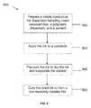
- FIG. 9is a flow chart 900 illustrating steps in a process to form a metallic film from a metallic ink. Some or all of these steps are described in detail in the examples below.
- a stable conductive ink dispersion including metal nanoparticles, a polymeric dispersant, and a solventis prepared.
- the inkis applied to a substrate.
- the inkis pre-cured.
- the inkis cured to form a conductive metallic ink.
- BYK®-378was added to an ink solvent mixture (DT) including 2-butoxyethyl acetate (D) and propylene glycol monomethyl ether acetate (T). As shown in Table 2 below, the solvent surface tension decreased by about 2 mN/M from 29 mN/m without BYK®-378 to about 26.78 mN/m with 1 ⁇ 2 wt % BYK®-378. A reduced solvent surface tension of about 26 ⁇ 27 mN/m was shown to substantially eliminate pin holes in the resulting coating.
- DTink solvent mixture
- D2-butoxyethyl acetate
- Tpropylene glycol monomethyl ether acetate
- Styrene maleic anhydride copolymer SMA® 1440 and its hydrolyzed water soluble derivative SMA® 1440H Solutionwere added to the solvent described in Example 1 (DT) along with 17 wt % copper loading. As seen in Tables 3 and 4, based on a scale of 1 (poor adhesion) to 10 (excellent adhesion), both SMA® 1440 and SMA® 1440H increased the coating adhesion of uncured copper film to KAPTON® substrate.
- SMA® 1440 and SMA® 1440Hmay also serve as adhesion promoters for cured copper films.
- SMA® 1440 and SMA® 1440His effective to achieve the desired improvement in adhesion for both cured and uncured copper films.
- a mixture of copper wetting promoter MA1610, surface tension modifier BYK®-378, and film adhesion modifier COLA®SOLV IESwas added to a conductive copper ink formulation. As shown in Table 6 below, the additives improved coating uniformity, adhesion to a KAPTON® substrate, and copper film resistivity.
- the neutralized form of this acidic polymeris referred to as HCS—N.
- HCS and HCS—Nare available as suspensions in aqueous ethanol. Copper nanoparticles were added to HCS/HCS—N to yield a suspension within a suspension.
- a water-based ink including copper nanoparticles and a solution of a conducting polymer PT(shown in Example 3) was prepared.
- the PTwas dissolved in aqueous alcohol, and copper nanoparticles were added to alcohol/PT solution to form a dispersion.
- a water-based ink including copper nanoparticles and a solution including PT (shown in Example 3) and BYK® wetting agents and surface tension modifierswas prepared.
- a water-based ink including copper nanoparticles and SMA® 1440H dispersantwas prepared.
- a water-based ink including copper nanoparticles and glyoxylic acid or oxalic acidwas prepared.
- each of these inkswas coated on polyimide (KAPTON®). The coating was pre-cured and photosintered. The dispersion-quality was evaluated under centrifugation conditions. Other additives, including BYK®-349, BYK®-DYNWET800, isostearyl ethylimidazolinium ethosulfate and alcohols were added to some of these inks to promote good wetting properties and adhesion properties. For each of these inks, resistivity of the final metallic film was a range of about 5 to about 50 ⁇ cm range.
- Resistivities below 10 ⁇ cmwere obtained for films formed from water-based copper inks including combinations of HCS, HCSN, SMA, PT, BYK®-349 and BYK®-DYNWET800. Resistivities below 20 ⁇ cm were obtained for films formed from water-based copper inks including glyoxylic acid. Resistivities below 200 ⁇ cm were obtained for films formed from water-based copper inks including oxalic acid and polyvinylpyrrolidone.
- the resistivitydecreased from 19 to 8 ⁇ cm with no loss of adhesion when 0.2 wt % PT was added to the aqueous ink with BYK®-DYNWET800 and SMA® 1440H.
- a mixture of water and alcoholwas used as a vehicle for formulating copper inks.
- the water contentranged from about 50 wt % to about 80 wt %.
- the alcohol contentranged from about 10 wt % to about 50 wt %.
- Alcoholsincluding isopropanol (IPA), isobutyl alcohol, ethanol, polyvinyl alcohol, ethylene glycol, and combinations thereof were used.
- Amines, polyvinylpyrrolidone (PVP), polyethylene glycol, isostearyl ethylimidazoliniurn ethosulfate, and oleyl ethylimidazolinium ethosulfatewere used as dispersants.
- water, IPA, and PVPwere mixed with copper nanoparticles to form a copper ink.
- the inkwas coated on a polyimide substrate to form a film.
- the filmwas photosintered to yield copper conductors.
- a copper ink with a H 2 O/IPA vehicle system and DISPERBYK®-111 as the dispersantyielded a film with a resistivity of 4.85 ⁇ cm.
- a weight ratio of IPA:H 2 O of 2:1 to 3:1was desirable with the addition of adhesion promoter additives, such as COLA®SOLV IES and SMA® 1440H to the H 2 O/IPA vehicle system.
- a mixture of cyclohexanol/IPA/H 2 Owas prepared for use as a vehicle for a copper ink formulation.
- Preferred compositionsincluded a water content of about 10 wt % to about 50 wt %, a cyclohexanol content of about 40 wt % to about 60 wt %, and a ratio of H 2 O:IPA of about 1:1 to about 1:2.
- a resistivity of 8 ⁇ cmwas achieved for a copper ink with a copper nanoparticle loading of about 10 wt % to about to 15 wt %, with a cyclohexanol/H 2 O/IPA vehicle and a dispersant selected from phosphoric acid modified phosphate polyester copolymers DISPERBYK®-11, DISPERBYK®-190, DISPERBYK®-194, the sulfonated styrene maleic anhydride ester SMA® 1440H, or any combination thereof.
- a mixture of isobutanol/IPA/H 2 Owas prepared for use as a vehicle for a copper ink formulation.
- Preferred compositionsincluded a water content of about 10 wt % to about 30 wt %, a isobutanol content of about 20 wt % to about 80 wt %, and a ratio of H 2 O:IPA of about 1:1 to about 1:2.
- a resistivity of 20 ⁇ cmwas achieved for a copper ink with a copper nanoparticle loading of about 10 wt % to about to 15 wt %, with a isobutanol/H 2 O/IPA vehicle and a dispersant selected from phosphoric acid modified phosphate polyester copolymers DISPERBYK®-111, DISPERBYK®-190, DISPERBYK®-194, COLA® SOLV IES, the sulfonated styrene maleic anhydride ester SMA® 1440H, or any combination thereof.
- the dispersionalso included 1-5 wt % dimethyl sulfoxide and 1-5 wt % oxy-bis-ethanol.
- the solutionwas agitated for at least 20 minutes to break up any agglomerated copper nanoparticles and to mix the dispersion.
- Copper filmswere deposited by the draw-down process onto a flexible polyimide substrate. Following this, a pre-cure process at 100° C. in air was employed to evaporate the water and solvents from the deposited film. The pre-cure step required at least 15 minutes to ensure that the water and solvents were removed, and that the resulting material was dry.
- An ink-jet printerwas also used to print this copper ink onto a polyimide substrate. After ink-jet printing, a pre-cure process of heating at 100° C. in air was carried out to evaporate the water and the solvents, and to ensure that the resulting printed material was dry.
- An optical flash systememploying a high-power pulsed xenon lamp able to deliver up to 15 J/cm 2 energy density with a pulse width of from 0.01 to 2000 ⁇ sec, was then used to cure the printed and dried copper inks.
- This optical curing stepwas carried out in air at room temperature. After this curing process a resistivity of 7 ⁇ 10 ⁇ 6 ⁇ cm was achieved with films printed by both draw-down and ink-jet printing methods.
- FIG. 7which depicts patterns 700 printed with this copper ink on a polyimide substrate 702 , the copper nanoparticles are fused during the very short curing time of the xenon flash, with little or no damage to the substrate.
- any copper oxides that are present on the surface of the copper nanoparticlesare at least partially photoreduced, as shown in the X-ray diffraction patterns in FIG. 8 , which were taken on samples before 800 and after 802 the flash curing process with the xenon lamp.
- a 0.1 wt % to about 1 wt % dispersion of the conductive polymer PTwas prepared in water. Copper nanoparticles, with a size ranging from about 2 nm to about 100 nm, were added to this dispersion in a glove box to form a dispersion with a range of about 15 wt % to about 65 wt % copper. The solution was agitated for about 20 minutes to break up any agglomerated copper nanoparticles and mix the dispersion. A stable dispersion, or copper ink, was obtained after agitation. Minimal settling of the copper nanoparticles was noted.
Landscapes
- Chemical & Material Sciences (AREA)
- Engineering & Computer Science (AREA)
- Dispersion Chemistry (AREA)
- Materials Engineering (AREA)
- Wood Science & Technology (AREA)
- Organic Chemistry (AREA)
- Life Sciences & Earth Sciences (AREA)
- Physics & Mathematics (AREA)
- Spectroscopy & Molecular Physics (AREA)
- Microelectronics & Electronic Packaging (AREA)
- Nanotechnology (AREA)
- Inks, Pencil-Leads, Or Crayons (AREA)
- Conductive Materials (AREA)
Abstract
Description
- This application claims the benefit under 35 U.S.C. §119(e)(1) of U.S. provisional application Ser. No. 61/034,087, filed Mar. 5, 2008, and U.S. provisional application Ser. No. 61/113,913, filed Nov. 12, 2008, both of which are hereby incorporated by reference herein.
- The present invention is related to conductive inks.
- Printed conductive films have the potential to lower manufacturing costs for microelectronics and large area electronics. Recently, metal nanoparticles having consistent size and shape have been developed. The inventors have discovered that these nanoparticles may be used to prepare well-dispersed inks. These metallic ink dispersions may be used for printing conductors, thereby making the direct writing of electronic circuits possible. Silver and gold nanoparticle-based inks are beginning to be used for printing electronics. These metals may be used because of their relatively high stabilities toward oxidation by molecular oxygen. Copper, with a resistivity of 1.7 μΩ·cm, has been extensively used for electronics and microelectronic chips. Moreover, copper is less costly than silver or gold, thereby making it a more attractive material for printed conductors. Oxidation of copper nanoparticles during printing and curing, however, has been difficult to avoid.
- To achieve a stable dispersion of metal nanoparticles, dispersants are adsorbed onto the surface of the nanoparticles. The function of these dispersants is to keep the individual nanoparticles apart and prevent them from aggregating and agglomerating together. Dispersants may be organic polymers or long chain molecules. Such compounds have high boiling points or decomposition temperatures, and are difficult to remove during a curing process. Any residues from these dispersants remaining in the cured metallic films will result in higher resistivities being obtained in the metal conductor that is formed because these dispersants and their decomposition products are non-conducting organic compounds, or insulators.
- In one aspect, a conductive ink includes metallic nanoparticles, a polymeric dispersant, and a solvent. In some implementations, the polymeric dispersant may be ionic, non-ionic, or any combination of ionic and non-ionic polymeric dispersants. The boiling point of the polymeric dispersant may be less than about 150° C. In some implementations, the solvent includes water, an organic solvent, or any combination thereof. The boiling point of the organic solvent may be less than about 150° C. In certain implementations, the conductive ink includes a stabilizing agent, an adhesion promoter, a surface tension modifier, a defoaming agent, a leveling additive, a rheology modifier, a wetting agent, an ionic strength modifier, or any combination thereof. In some implementations, the metallic nanoparticles comprise about 10 wt % to about 60 wt % of the ink. In certain implementations, the polymeric dispersant comprises about 0.5 wt % to about 20 wt % of the ink.
- In another aspect, a conductive ink includes about 15 wt % to about 65 wt % copper nanoparticles, a vehicle comprising about 10 wt % to about 50 wt % alcohol and about 50 wt % to about 80 wt % water, and a dispersant. The alcohol may be isopropanol, isobutyl alcohol, ethanol, polyvinyl alcohol, ethylene glycol, or combinations thereof. In some cases, the dispersant may be polyvinylpyrrolidone, polyethylene glycol, isostearyl ethylimidazolinium ethosulfate, oleyl ethylimidazolinium ethosulfate, or combinations thereof. In some cases, the dispersant may be phosphoric acid modified phosphate polyester copolymers, sulfonated styrene maleic anhydride esters, or combinations thereof.
- In some implementations, the vehicle includes about 10 wt % to about 50 wt % water, about 40 wt % to about 60 wt % cyclohexanol, and an amount of isopropanol such that a ratio of water to isopropanol is between about 1:1 and about 1:2. In other implementations, the vehicle includes about 10 wt % to about 30 wt % water, about 20 wt % to about 80 wt % isobutanol, and an amount of isopropanol such that a ratio of water to isopropanol is between about 1:1 and about 1:2.
- In some implementations, the conductive ink is curable to form a film with a resistivity of less than about 10 μΩ·cm, less than about 20 μΩ·cm, or less than about 200 μΩ·cm. The film may be substantially free of imperfections, such as pin holes.
FIG. 1 illustrates a dispersant for metallic particles with both cationic and anionic polymeric groups.FIG. 2 illustrates the chemical structure of 3,4-polyethylenedioxythiophene-polystyrenesulfonate (PEDOT:PSS).FIG. 3 illustrates the acid-base equilibrium of a substituted polythiophene.FIG. 4 illustrates a double layer polymeric dispersant on a metal nanoparticle.FIG. 5 illustrates the chemical structure of selected non-ionic surfactants.FIG. 6 illustrates the chemical structure of a pigment wetting agent obtained by hydrolysis of a styrene-maleic anhydride copolymer resin.FIG. 7 illustrates ink-jet printed patterns from copper ink prepared with a conductive polymer.FIG. 8 illustrates X-ray diffraction patterns of copper oxides and copper nanoparticles in copper ink before and after photonic curing.FIG. 9 is a flow chart illustrating steps in a process of forming metallic film from metallic ink.- Metallic inks suitable for forming conductors may be formulated with metal nanoparticles, conductive polymers, and a carrier system, such as water, organic solvents, or a combination thereof. The nanoparticles may be, for example, copper, silver, nickel, iron, cobalt, aluminum, palladium, gold, tin, zinc, cadmium, etc., or any combination thereof. The nanoparticles may be about 0.1 μm (100 nm) in diameter or smaller. Steps to form a stable dispersion from a metallic nanopowder may include wetting the powder, breaking up agglomerates in the powder (de-agglomerating), and stabilizing the dispersed particles to inhibit flocculation. In some cases, a dispersant or surfactant may be added to facilitate de-agglomeration of the powder. In some cases, the dispersant that provides the best performance at one step of the process may not provide the best performance at another step. Thus, it may be beneficial to incorporate more than one dispersant or surfactant.
- Unlike the insulating residues of common dispersants, conductive organic compounds such as conductive polymers may not act as an insulating defect in the metallic conductors, but instead may act as a parallel-serial resistor (R2) with a metallic conductor (R1). The resistivity of the conductive polymer (ρ2) may be as low as 0.001 Ω·cm. By comparison, the resistivity of the metallic conductors (ρ1) is in the region of 10−6Ω·cm. The total resistance (R) may be described as:
- where
- and S1 and S2 are the cross-sectional areas of the conductive polymer and the fused nanoparticles, respectively. The S2/S1 ratio is smaller than 0.1. Thus, R≦R1, meaning that the total resistance is smaller than that of the metallic conductor, but not significantly smaller. Thus, residual conductive polymer may not increase the resistivity as much as insulating residues from non-conducting dispersants. If the conductive polymer is also the dispersant for metallic nanoparticles, the resistivity of the resulting metallic films may be significantly reduced, due at least in part to limited or no additional contamination from residual non-conducting dispersants. In some cases, metal inks may be cured to obtain conductive metal films with resistivities close to those of the bulk metal conductor itself.
- Steric stabilization, electrostatic stabilization, or a combination thereof may be used to prepare dispersions that remain stable during storage and deposition, thus yielding uniform and consistent coatings. Steric stabilization of metal nanoparticles may be achieved with a non-ionic dispersant or polymer. Steric contributions include interactions between the surface of the metal nanoparticles and functional groups of polymers or long chain organic molecules, thereby making direct contact between the metal particles (e.g., formation of aggregates and agglomerates) less likely. Strong interaction between the polymers or the long chain molecules and the solvent or water may inhibit the polymers from coming too closely into contact with one another. Electrostatic stabilization occurs when charged (e.g., substantially equally charged) nanoparticles repel each other, thereby allowing the metal nanoparticles to stay apart and substantially avoid contact with each other. Electrostatic stabilization of a charged metal nanoparticle may be achieved with an ionic dispersant or polymer. Dispersants with a high hydrophile-lipophile balance (HLB) may be used with aqueous dispersions, and dispersants with a low HLB may be used with dispersions in non-polar organic liquids.
- Nanoparticle dispersion may also be enhanced by charging a surface of a metal nanoparticle. Metallic nanoparticles may have an oxide layer on their surface. The oxide layer may have a thickness of, for example, about 1 nm to about 20 nm. In the presence of water, an acid-base reaction may occur, forming a hydroxide layer on the surface. The hydroxide layer may adsorb or lose protons to produce a positively or negatively charged surface. Thus, charging through proton gain or loss, or charging by adsorbed charges, may be involved in achieving a good dispersion. At low pH, the hydroxide surface may react with protons to produce a positively charged surface. In contrast; at high pH, protons may be removed to produce a negatively charged surface. Thus anionic and cationic dispersants may be adsorbed onto the surface of metal nanoparticles under conditions that depend on the pH of the solution or dispersion. Therefore, charged conductive polymers having oppositely charged polyacid functionalities for charge compensation may be used to advantageously disperse metal nanoparticles in aqueous inks.
- Anionic polymeric dispersants, cationic polymeric dispersants, or a combination thereof may be used to form electrostatic dispersions with charged metallic surfaces in aqueous media. Since, inorganic particle surfaces may be heterogeneous, with both positive and negative sites, dispersants having negatively and/or positively charged anchor groups may be advantageous. Positively charged nanoparticles may form an electrostatic dispersion with a dispersant containing both anionic and cationic polymer chains.
FIG. 1 illustrates an embodiment of a dispersant with a combination of both anionic100 and cationic102 polymeric groups for the dispersion ofmetallic particles 104. In some cases, the metallic surface may be heterogeneous, having both negatively and positively charged sites. With both anionic and cationic groups present in the dispersant, the dispersant is compatible with the different charge regions on the metal nanoparticles, and a stable dispersion may be achieved. - Conductive polymers including, but not limited to, conductive polythiophenes, conductive polyanilines, metallophthalocyanines, and metalloporphyrins may be used to prepare aqueous metallic inks. 3,4-polyethylenedioxythiophene-polystyrenesulfonate (PEDOT:PSS), illustrated
FIG. 2 , is an example of a conducting polymer that may be used to prepare aqueous metallic inks. The substituted polythiophene (PT) illustrated inFIG. 3 is another example of a conductive polymer that may be used to prepare aqueous metallic inks. In an implementation in which ionic polythiophene conducting polymers are used to prepare aqueous metallic inks, the positive charge may be located within a polythiophene network. In another implementation, the positive charge may be appended as a cation such as, for example, sodium. In each case, the multifunctional structure allows for low concentrations to be used to achieve stable nanoparticle dispersions. - Conducting polymers with multiple binding sites may partially surround a metal nanoparticle, thereby keeping it from aggregating or agglomerating.
FIG. 4 illustrates a double layer of apolymeric dispersant 400 withhead group 402 andtail group 404 on ananoparticle 406. Thenanoparticle 406 may be, for example, copper. This multi-site attachment of a polymer to a nanoparticle leads to a thermodynamic advantage over a dispersant that only attaches via a single site. Thehead group 402 may include, for example, amines, cationic alkylammonium groups, carboxylic acids, sulfonic acids, and phosphoric acid groups, along with their salts that have carboxylate, sulfonate and phosphate or phosphonate groups. - In addition to the thermodynamic advantage that is gained by having multiple attachment points between the
nanoparticle 406 and thehead group 402 of a conductive polymer, there is also an advantage in the conducting polymer having a tail group to it. The tail group may be a long chain functional group able to bend and rotate, sweeping out a large “excluded volume” that cannot be easily occupied by other nanoparticles, thus inhibiting other metal nanoparticles from approaching closely to the metal nanoparticle associated with the dispersant and aggregating or agglomerating with the dispersed metal nanoparticle. For example, long chain alkyl or alkoxy functionalities have a high degree of conformational flexibility, which allows them to create a high exclusion volume. Another advantage of a high exclusion volume is that it allows for a low concentration of dispersant to be used, and therefore, only a small quantity of dispersant to be removed during the curing process. - A
dispersant 400 may be selected such that thehead group 402 is chemically compatible with or preferentially associates with thenanoparticle 406, and thetail group 404 is chemically compatible with or preferentially associates with the vehicle (solvent). In a dispersion, thedispersant 400 may act as a molecular bridge between thenanoparticle 406 and the vehicle, thereby keeping the nanoparticles separated by one or more molecular layers. The solubility of thetail group 404 of thedispersant 400 in the vehicle is also a factor in the selection of a dispersant for a given ink formulation. - The
head group 402 of adispersant 400 may be selected such that the functionality of the group is compatible with themetal nanoparticle 406 in an ink formulation. That is, the attraction between thehead group 402 and thenanoparticle 406 is advantageously stronger than the attraction between the head group and the vehicle in the system. The attraction may include charge attraction, specific donor-acceptor bands between unshared electron pairs and empty molecular orbitals, hydrogen bonding, electrostatic field trapping of polarizable molecules, or any combination thereof. For metal nanoparticles with positively or negatively charged surfaces, conductive metallic inks have been prepared using anionic components such as halide or carboxylate ions, or cationic components such as hydrogen ions or group I cations, respectively. When thehead group 402 is a polymer, the polymer may provide multiple anchoring sites and thus multiple site coverage of thenanoparticle 406. - In some embodiments, a dispersion of metal nanoparticles is formed by adding the nanoparticles to a dispersion of a conductive polymer. A dispersion of the conductive polymer may be formed by adding the polymer to a carrier. The carrier may be, for example, water, an organic solvent, or any combination thereof. The pH of the dispersion may be from about 1 to about 12. Metal nanoparticles may be added to the conductive polymer dispersion to form a metal nanoparticle dispersion.
- Conductive metallic inks may include a loading concentration of metallic nanoparticles in a range from about 10 wt % to about 65 wt %, or from about 15 wt % to about 60 wt %, of metal nanoparticles.
- An effective amount of dispersant may be used to achieve monolayer coverage of the nanoparticles with the head groups of the dispersant such that the surface of nanoparticle is substantially inaccessible to other nanoparticles for aggregation or agglomeration. In some ink formulations, for example, an effective weight percentage of dispersant may be in a range from about 0.1 wt % to about 20 wt %, or about 0.5 wt % to about 10 wt %. Coverage of less than a monolayer leaves open sites on the nanoparticle that may cause agglomeration. If a second monolayer of dispersant is present on the nanoparticle, the second layer may be oriented in the opposite direction from the first layer, thereby reducing the compatibility of the nanoparticle with the solvent.
- Polymeric dispersants may have higher viscosities than liquids used as vehicles in conductive inks. A higher viscosity promotes forming of a dispersion suitable for ink-jet printing methods. Also, the presence of multiple nanoparticle binding sites allows polymeric dispersants to be used at lower concentration than monomeric dispersants with single binding sites, aid still confer monolayer coverage of the metal nanoparticle. Lower concentrations of the dispersant are favorable because less organic material remains after the curing process.
- Other additives such as, for example, dimethyl sulfoxide and oxy-bis-ethanol, may be present in the dispersion in various amounts such as, for example, about 1 wt % to about 5 wt %. In some implementations, polyacids, such as polystyrenesulfonic acid, may be used for charge compensation in an ink formulation.
- When agglomerates are present in a nanopowder, de-agglomeration facilitates formation of a stable dispersion. In some cases, nanoparticles in a metallic nanopowder may be agglomerated through a salt bridge, including a soluble salt precipitated in the formation of the nanopowder. These salt bridges may be dissolved by a dispersant to break up the agglomerates. Dispersants that infiltrate crevices between nanoparticles in a nanopowder may also reduce the energy required to propagate cracks through the solid, and may thereby function as grinding aids.
- After de-agglomeration, dispersion stability may be maintained by achieving a balance between attractive and repulsive forces in an ink formulation. The maintenance of a dispersion may be assisted by mechanically breaking up the agglomerates with a ball mill or other device, sonication (e.g., ultrasonication), and the like. These mechanical processes may be carried out in the presence of a dispersant to reduce the occurrence of re-agglomeration after mechanical agitation.
- Conductive metallic inks with good dispersion may be printed by processes including, for example, draw-down or ink-jet printing. Other printing methods, including spin-casting, spraying, screen printing, flexo printing, gravure printing, roll-to-roll coating, and the like, may also be used for depositing conductive metallic inks. The inks may be deposited on substrates, including flexible substrates such as polyimide (e.g., KAPTON®, available from E.I. du Pont de Nemours and Company, Wilmington, Del.) liquid crystalline polymers (LCPs), MYLAR® and polyethylene terephthalate (PET).
- After the ink has been applied to a substrate, a pre-cure process may be conducted in air and at temperatures less than about 150° C. The pre-curing step facilitates drying of the printed or coated metal nanoparticles before curing, thereby reducing rapid evaporation of volatile compounds during curing, and substantially eliminating film discontinuities and rough surfaces resulting from this rapid evaporation.
- The printed and dried inks may be cured. Curing methods include an optical flash system, a pulsed laser with suitable wavelengths, and other short-pulsed lamps. The printed metal inks, after the pre-cure drying step, may be black and therefore able to absorb light over a broad range of wavelengths. The curing process may be carried out at room temperature in air. During an optical (or photonic) curing process, the metallic film may be directly heated by the absorbed light. Non-metallic portions of the substrate may not be directly heated by the absorbed light. If the light intensity is sufficiently high (for example, on the order of a few Joules per square centimeter) and the pulse is sufficiently short (for example, on the order of 300 microseconds or less), then the optical energy delivered to the film may melt the metal nanoparticles. The melted nanoparticles may fuse together. The short duration of the pulse may reduce the amount of energy absorbed by the substrate material.
- For some conductive inks, such as copper inks, curing may be achieved by photosintering. During photosintering, metallic nanoparticles are adhered together during photonic curing to form metallic films. Lasers, including continuous and pulsed lasers (e.g., nanosecond to femtosecond lasers) may be used to sinter metallic inks into metallic conductors. The photosintering process may occur on a time scale from microseconds to less than a millisecond. For passivated metallic nanoparticles, the metal oxide layer may be photoreduced to elemental metal, resulting in high-purity metallic conductors. In some-cases, heat from photosintering causes a welding effect between the metal and plastics having relatively low melting points, yielding excellent adhesion between these metallic conductors (or films) and the substrate without the use of binder materials. In the case of passivated copper nanoparticles, photosintering allows the layer of copper oxides to be photoreduced into metallic copper, and fused together to form copper conductors.
- For conductive films formed by photosintering copper inks with non-ionic dispersants, a resistivity as low as about 3.6 μΩ·cm to about 10 μΩ·cm may be achieved (1.7 μΩ·cm for bulk copper). For conductive films formed from copper inks including ionic dispersants or ionic and non-ionic dispersants, resistivity as low as about 2.3 μΩ·cm to about 10 μΩ·cm may be achieved.
- The use of such photonic curing to sinter the copper nanoparticles allows for the curing process to be carried out in air. Photonic curing reduces the formation of non-conducting copper oxides that may occur during thermal curing in air. The presence of non-conducting copper oxides in copper films results in high resistivities. In contrast, the photonic curing process occurs in a fraction of a second, and no significant oxidation occurs before the copper cools back to ambient temperature. During the curing process, the copper nanoparticles are fused during the very short curing time, while little or no damage occurs to the substrate, and copper oxides that are present on the surface of the copper nanoparticles are at least partially photoreduced.
- For cured films formed from copper nanoparticle ink, a resistivity of about 7×10⁻⁶Ω·cm, or about 4 times greater than the resistivity of bulk copper, may be achieved with both draw-down and ink-jet printing methods. Copper inks that may be cured in air to give copper conductors that have resistivities in the μΩ·cm range have a very wide range of applications, including fabrication of printed circuit boards (PCBs), flexible electronics, solar panels, and other applications where a metallic conductor needs to be patterned or deposited.
- The excluded volume of non-ionic (steric) dispersants represents the space “occupied” by the tail group of the dispersant, which may be a flexible alkyl (or ethoxy) chain. This space is substantially free from other nanoparticles. A larger excluded volume separates metal nanoparticles more effectively than a smaller excluded volume, and provides a high level of coverage of the nanoparticle with a low concentration of dispersant.
- The following exemplary non-ionic polymers are useful as modifiers in the formulation of inks that are photonically curable to yield good conductors:
- 1. Surfactants (such as TRITON® X-100, TRITON® X-15, TRITON® X-45, TRITON® QS-15, available from Roche Diagnostics GmbH, Germany).
- 2. Linear alkyl ethers (such as COLA® CAP MA259 and COLA® CAP MA1610, available from Colonial Chemical, Inc., South Pittsburg, Tenn.).
- 3. Quaternized alkyl imidazolines (such as COLA®SOLV IES and COLA®SOLV TES, available from Colonial Chemical, Inc.).
- 4. Polyvinylpyrrolidone (PVP), polyvinyl alcohol (PVA), polyethylene glycol (PEG), and polysiloxanes, polystyrene, alkyl substituted thiphone polymers (such as ADS 304PT and ADS 306PT, available from American Dye Source, Inc., Canada), styrene maleic anhydride copolymer (such as SMA® 2625, SMA® 17352, SMA® 1440 Flake, SMA® 3000, available from Elf Atochem, UK), and polybutadiene adducted with maleic anhydride (such as RICOBOND® 1756 and RICOBOND® 1731, available from Elf Atochem).
- The following exemplary ionic polymers are useful as modifiers in the formulation of inks that are photonically curable to yield good conductors:
- 1. Copolymers with ionic groups, including carboxylic acid modified polyester copolymers (such as DISPERBYK®-111 and 110, available from BYK Chemie, Germany) and high molecular weight block copolymers with pigment affinic groups (such as DISPERBYK®-182, 190, 191, 192 and 194, available from BYK Chemie).
- 2. Aqueous ammonium solutions of styrene maleic anhydride copolymer (such as SMA® 1440H Solution, an aqueous solution of the ammonium salt of SMA® 1440, available from Elf Atochem) or hydrolyzed styrene maleic acid anhydride copolymer, both of which exhibit good wettability to metallic nanoparticles in an aqueous matrix and may be used as a dispersant in a water-based ink formulation.
- 3. Conductive polythiophene (PT) with substituted alkyl chains (such as ADS2000P, available from American Dye Source, Inc.), water-soluble sulfonated polystyrene, and a mixture of the polystyrene and polythiophene colloid solutions (such as HCS—P, HCS—N, available from H. C. Starck GmbH, Germany).
- Solvents such as, for example, 2-butoxyethyl acetate, propylene glycol monomethyl ether acetate, diethylene glycol monoethyl ether acetate, ethylene glycol butyl ether, cyclohexanone, cyclohexanol, 2-ethoxyethyl acetate, ethylene glycol diacetate, water, and the like, may be used with both non-ionic and ionic polymer dispersants to formulate conductive metallic inks.
- In some cases, both non-ionic and ionic dispersants, such as those listed above, may be used in an ink formulation to form more stable dispersions. Solvents described above, or any combination thereof, may be used as vehicles for ink formulations including non-ionic and ionic dispersants. Solvents including mixtures of i) 2-butoxyethyl acetate and propylene glycol monomethyl ether acetate, ii) 2-ethoxyethyl acetate and propylene glycol monomethyl ether acetate, iii) 2-ethoxyethyl acetate and amyl acetate, and iv) ethylene glycol diacetate and propylene glycol monomethyl ether acetate are effective vehicle systems for ink formulations with both ionic and non-ionic dispersants.
- Metallic inks may be formulated to yield metallic-films with high conductivity. For example, ink formulations with low boiling-point solvents and dispersants leave little organic residue after film formation (e.g., by photosintering), resulting in films with high conductivity. Low boiling-point solvents include, for example, isobutyl alcohol, isopropyl alcohol, ethanol, toluene, butylbenzene, butyl acetate, water, and the like. Low boiling-point dispersants include, for example, amines with relatively low molecular weight, such as hexyl amine, octylamine, and the like These low boiling-point vehicles and dispersants may have boiling points less than about 150° C., or may be vaporized when a pre-cure process at temperatures less than about 150° C. is applied to the coated inks. For the amines with boiling points less than about 150° C., much of the dispersant will be vaporized during the pre-cure process. In an example, high-purity copper films with a resistivity of about 2.5 μΩ·cm may be formed by photosintering ink formulations with low boiling point vehicles and dispersants.
- Additives and modifiers may be used to enhance performance of conductive metallic inks. The properties and amounts of these additives and modifiers may be different for each conductive metallic ink, for each substrate, for each printing method, and the like. These differences may result from different surface energies of substrates, different adhesion properties of substrates, requirements of different printing methods such as ink-jetting, and different strategies used to sinter the metallic inks into metal conductors. The additives and modifiers may be selected to be chemically compatible with both the vehicles and dispersants used in the formulation of the inks. Also, because the surface tension of solvent- and water-based inks may be different, different additives and modifiers may be needed to maintain the desired contact angle between the ink and the substrate.
- Additives and modifiers used in conductive metallic inks may act as rheology modifiers, wetting agents, adhesion promoters, binders, defoaming agents, leveling agents, ionic strength modifiers, and the like. Additives and modifiers may be advantageously selected to tailor ink properties for different ink formulations, substrates, and application methods. For example, selection of agents and modifiers allows careful control of ink properties needed for use with a variety of substrates, including modification within substrate types, as well as for use with different delivery methods such as ink-jetting or aerosol jetting, including formulations targeted for specific printer manufacturers, model types, and print heads.
- Selection of additives and modifiers for a conductive ink formulation may depend on physico-chemical properties of the vehicle system, the substrate, or any combination thereof. For example, organic-solvent-based inks may have a low surface tension and a small contact angle on many substrates, while a wetting agent may be needed to impart water-based inks with reduced surface tension and desired wetting properties. Substrates with a high surface energy, including flexible substrates such as polyimide, require different additives and modifiers than substrates with a low surface energy, such as glass, silicon, or low surface energy polymeric substrates. Variation in substrate porosity, and consequently, differences in absorption of the conductive ink, may also influence selection of additives and modifiers for a conductive ink formulation.
- Additives and modifiers may be chosen such that a conductive ink is able to adhere to flexible substrates, such as polyimide and liquid crystal polymers, while also being able to form conductive patterns or films with electrical resistivities on the same order of magnitude as the analogous bulk metal. These additives provide the ink with wetting and surface tension properties to allow compatibility with the substrate surface and printing equipment, such as ink-jet nozzles, and help maintain a uniform dispersion needed for homogeneous print quality. These additives may be, for example, polymeric materials having different chain lengths, terminal end groups, side chains, and co-polymeric chains that introduce the desired properties into the conductive inks. In some cases, these polymers enhance the dispersion action of the dispersant. Modifiers and additives may also be used to enhance ink shelf life stability, final cured resistivity, and coating appearance.
- Properties such as dispersion, ink rheology, adhesion, and coating quality may be selectively enhanced by certain modifiers and additives. For example, dispersion stabilizing agents (such as
DISPERBYK® 111, 110, 180, and 190), anti-settling agents (such as BYK®-410 and 420), or any combination thereof may be added to conductive inks to enhance the ink shelf life stability and ink-jet-ability. In addition, ink rheology may be improved by rheology-modifying polymers (such as BYK®-410 and 420), by increasing the vehicle viscosity with addition of higher viscosity solvents (such as isobutyl alcohol, terpineol, glycerol, and the like), or any combination thereof. Adhesion enhancement may be achieved by adding adhesion promoters, such as styrene maleic anhydride copolymers (such as SMA® 1440H Solution and SMA® 1440 Flake), linear alkyl ethers (such as COLA® CAP MA259 and COLA® CAP MA610), quaternized alkyl imidazolines (such as COLA® SOLV IES and COLA® SOLV TES), and the like, into ink formulations. IES (or isostearyl ethylimidazolinium ethosulfate) is a biodegradable ionic liquid that reduces the static charge on metallic surfaces and improves adhesion of conductive inks. - Ink coating appearance or quality, as determined by coating uniformity and the absence of holes, may be improved by modifiers or additives that reduce ink surface tension, enhance metal wettability, promote ink defoaming, and the like. Surface tension modifiers such as, for example, BYK®-DYNWET800, BYK®-381, BYK®-346, and BYK®-378 (available from BYK Chemie), may be added into an ink formulation to reduce ink surface tension and improve metal wettability. Defoaming agents such as, for example, BYK®-066N, BYK®-141, BYK®-052, BYK®-067A, BYK®-1752, BYK®-080A, and BYK®-020 (available from BYK Chemie) may be used to reduce ink coating pinholes.
- Some of the modifiers and additives noted above are listed in Table 1.
TABLE 1 Properties of additives used in conductive ink formulations Product Name Manufacturer Function Chemical Description MA026 Colonial Non-ionic surfactant Chemical, Inc. MA257 Colonial Non-ionic surfactant Chemical, Inc. MA259 Colonial Non-ionic surfactant Chemical, Inc MA1610 Colonial Non-ionic surfactant Alkoxylated alkene Chemical, Inc COLA ® SOLV Colonial Foam stabilizer Isostearyl ethylimidazolium IES Chemical, Inc ethosulfate COLA ® SOLV Colonial Foam stabilizer Oleyl ethylimidazolium ethosulfate TES Chemical, Inc SMA ® 1440H Elf Atochem Surfactant and dispersant Styrene-maleic anhydride copolymer SMA ® 2625 Elf Atochem Surfactant Styrene-maleic anhydride copolymer SMA ® 3000 Elf Atochem Dispersant Styrene-maleic anhydride copolymer SMA ® 17325 Elf Atochem Surfactant Styrene-maleic anhydride copolymer RICOBOND ® Elf Atochem Adhesion promoter Polybutadiene resin 1731 RICOBOND ® Elf Atochem Adhesion promoter Polybutadiene with maleic anhydride 1756 BYK ®-020 BYK ® Chemie Defoamer BYK ®-052 BYK ® Chemie Silicone-free defoamer BYK ®-066N BYK ® Chemie Silicone defoamer BYK ®-067A BYK ® Chemie Defoamer BYK ®-080A BYK ® Chemie Silicone defoamer BYK ®-110 BYK ® Chemie Wetting and dispersing BYK ®-141 BYK ® Chemie Defoamer BYK ®-180 BYK ® Chemie Wetting & dispersing Alkylolammonium salt of copolymer BYK ®-182 BYK ® Chemie Wetting & dispersing Block copolymer BYK ®-190 BYK ® Chemie Wetting & dispersing Block copolymer BYK ®-191 BYK ® Chemie Wetting & dispersing Copolymer BYK ®-192 BYK ® Chemie Wetting & dispersing Copolymer BYK ®-194 BYK ® Chemie Wetting & dispersing Copolymer BYK ®-346 BYK ® Chemie Silicone surfactant BYK ®-378 BYK ® Chemie Surface tension reducer BYK ®-381 BYK ® Chemie Leveler BYK ®-410 BYK ® Chemie Rheological additive BYK ®-420 BYK ® Chemie Rheological additive BYK ®-DYN BYK ® Chemie Silicone free additive Alcohol alkoxylates WET800 BYK ®-1752 BYK ® Chemie Defoamer - The compounds MA026, MA257, MA259, and MA1610 are non-ionic surfactants available from Colonial Chemical, Inc. with the structure H3C—(CH2)x—O—(CH2CH2O)y—CH2C(CH3)═CH2(see
FIG. 5 ). These compounds share a common structure but differ in cloud points, foam heights, and Draves Wetting. MA1610 has the shortest wetting time in the group, with a Draves Wetting (0.1% active) value of 6.0 seconds at 25° C. As an additive to conductive inks (e.g., copper inks), a low concentration of MA1610 (for example, about 0.1 wt % to about 0.2 wt %) gives a desirably low resistivity in the resulting conductive film as well as highly uniform coatings on KAPTON® substrates. - BYK®-378, a polyether modified polydimethylsiloxane with the structure [O—Si(CH3)2]n, is a surface-tension-reducing agent that causes slip without support foam. This material, compatible with both organic-solvent-based and water-based inks, may be used in an amount ranging from about 0.01 wt % to about 0.3 wt % to limit cratering and increase ink-substrate wetting. SMA® 1440H Solution (SMA), —[(CH(Ph)—CH2)—CH(CO2H)—CH(CONHCH3)n]—, shown in
FIG. 6 , is a pigment wetting agent (molecular weight 5,000 Daltons) obtained by the hydrolysis of a styrene-maleic anhydride copolymer resin. - BYK®-349 is a water-based, water-soluble additive that decreases the surface tension of water-based inks and promotes penetration and absorption of the ink into the substrate. This silicone surfactant provides a reduction in surface tension that leads to substrate wetting and leveling. In water, a surface tension of about 23 mN/m may be achieved at a dosage of 0.05 wt % BYK®-349. Similarly, this surface tension modifier may be used in very low concentrations to alter the properties of inks.
- BYK®-
DYNWET 800 is an alcohol alkoxylate that provides excellent reduction of the dynamic surface tension and thus improves substrate wetting as well. It is a silicone-free surface additive for aqueous systems. Depending on the formulation, a dosage of about 1 wt % to about 2 wt % has been shown to improve flow on a variety of substrates. - BYK®-381 for Inks is an ionic solution of a polyacrylic copolymer acrylic leveling additive that has little or no impact on surface tension. Added in a range of about 0.1 wt % to about 1 wt % of the total formulation, BYK®-381 improves the flow of coatings and also increases gloss, reducing surface defects such as craters and pinholes.
- BYK®-346 for Inks, a solution of a polyether modified dimethylpolysiloxane, reduces the surface tension in aqueous printing inks, improving substrate wetting and leveling without foam stabilization. This silicone surfactant does not substantially increase surface slip or impair recoatability. If higher surface slip is desirable, BYK®-307, BYK®-333, or any combination thereof may be used together with BYK®-346. BYK®-346 imparts desirable properties to conductive inks in a range of about 0.1 wt % to about 1 wt % of the total formulation, and exhibits a desirable impact on systems with about 3 wt % to about 7 wt % co-solvent, based on the total formulation. If higher levels of co-solvents are present, polymeric silicone additives such as BYK®-307 and BYK®-333 may be used in place of BYK®-346. If the co-solvent content is lower, BYK®-348 may be used in place of BYK®-346. The solvent-free version of BYK®-346 is available as BYK®-345.
- BYK®-410 and 420 may be used as stabilizing agents in metallic inks and pastes to enable long-term dispersion stability in formulations in which the difference in density between metallic particles and the liquid medium would otherwise result in phase separation. Stabilizing agents are weakly gel forming polymers where upon quiescent storage or very low shear they become semi-solid, thus inhibiting aggregation and sedimentation of particles suspended within. Upon shearing such a system beyond a yield stress, it becomes liquid and thus flows easily.
- In metallic inks and pastes, stabilizing agents may be added in small quantities to avoid significant increases in the resistivity of conductors cured from these materials. In one example, an organogel was prepared by adding BYK®-410 to a organic-solvent-based copper nanoparticle ink. The resistivity of this ink was compared to an analogous ink that did not contain BYK®-410 by draw-down printing a film of each ink and measuring the resistivity by four-point probe. It was found that 0.2 wt % BYK®-410 was sufficient to inhibit phase separation in the ink without significantly increasing resistivity (i.e., resistivity increased from 7 μΩ·cm without BYK®-410 to 9 μΩ·cm with BYK®-410). Analogous systems have been developed in aqueous media with the aqueous stabilizing agent BYK®-420. For the water-based ink, the final film resistivity increased from 3.3 μΩ·cm without BYK®-420 to 8 μΩ·cm with BYK®-420.
- The following examples are provided to more fully illustrate some of the embodiments of the present invention. It should be appreciated by those of skill in the art that the techniques disclosed in the examples that follow represent techniques discovered by the inventors to function well in the practice of the invention, and thus may be considered to constitute exemplary modes for its practice. However, those of skill in the art should, in light of the present disclosure, appreciate that many changes may be made in the specific embodiments that are disclosed and still obtain a like or similar result without departing from the spirit and scope of the invention.
FIG. 9 . is aflow chart 900 illustrating steps in a process to form a metallic film from a metallic ink. Some or all of these steps are described in detail in the examples below. Instep 902, a stable conductive ink dispersion including metal nanoparticles, a polymeric dispersant, and a solvent is prepared. Instep 904, the ink is applied to a substrate. Instep 906, the ink is pre-cured. Instep 908, the ink is cured to form a conductive metallic ink.- BYK®-378 was added to an ink solvent mixture (DT) including 2-butoxyethyl acetate (D) and propylene glycol monomethyl ether acetate (T). As shown in Table 2 below, the solvent surface tension decreased by about 2 mN/M from 29 mN/m without BYK®-378 to about 26.78 mN/m with 1˜2 wt % BYK®-378. A reduced solvent surface tension of about 26˜27 mN/m was shown to substantially eliminate pin holes in the resulting coating.
TABLE 2 Solvent surface tension reduction with BYK ®-378 Surface Tension (mN/m) of BYK ®-378 (wt %) DT-BYK ®-378 0 29 0~0.5 27.72 0.5~1 26.3 1~2 26.78 - Styrene maleic anhydride copolymer SMA® 1440 and its hydrolyzed water soluble derivative SMA® 1440H Solution were added to the solvent described in Example 1 (DT) along with 17 wt % copper loading. As seen in Tables 3 and 4, based on a scale of 1 (poor adhesion) to 10 (excellent adhesion), both SMA® 1440 and SMA® 1440H increased the coating adhesion of uncured copper film to KAPTON® substrate.
TABLE 3 Effect of SMA ® 1440 on coating adhesion SMA ® Coating adhesion of 1440 (wt %) in DT solvent with uncured copper film to 17 wt % Copper Loading KAPTON ® substrate (score of 1-10) 0 1 0~0.5 2 0.5~1 5 1~2.5 10 2.5~10 10 TABLE 4 Effect of SMA ® 1440H on coating adhesion SMA ® Coating adhesion 1440H (wt %) in water/ethanol of cured copper film to with 17 wt % Copper Loading KAPTON ® substrate (score of 1-10) 0 1 0~1.25 3 1.25~2.5 4 2.5~5 5 - Additional experiments indicated that SMA® 1440 and SMA® 1440H may also serve as adhesion promoters for cured copper films. A dosage of 0.1·15 wt %. SMA® 1440 and SMA® 1440H is effective to achieve the desired improvement in adhesion for both cured and uncured copper films.
- As seen in Table 5, addition of 0.1·0.5 wt % COLA®SOLV IES to a mixture of SMA® 1440H, BYK®-
DYNWET 800, and the conducting polythiophene (PT) (shown as the orange form inFIG. 3 ) improves the adhesion of a water-based copper ink to a KAPTON® substrate with a slight reduction in resistivity. TABLE 5 Effect of additives on coating adhesion and resistivity BYK ®- Adhesion score SMA ® 1440H DYNWET COLA ® SOLV on KAPTON ® Resistivity (wt %) 800 (wt %) IES (wt %) PT (wt %) (1-10) (μΩ · cm) 1~5 1~5 0 0 3 11 1~5 1~5 0 0.1~0.5 5 7 1~5 1~5 0.1~0.5 0.1~0.5 10 6.45 - A mixture of copper wetting promoter MA1610, surface tension modifier BYK®-378, and film adhesion modifier COLA®SOLV IES was added to a conductive copper ink formulation. As shown in Table 6 below, the additives improved coating uniformity, adhesion to a KAPTON® substrate, and copper film resistivity.
TABLE 6 Effect of additives on coating adhesion and resistivity. COLA ® Pre-sintering SOLV coating score MA1610 BYK ®-378 IES on KAPTON ® Adhesion score on Resistivity (wt %) (wt %) (wt %) (1-9) KAPTON ®(1-10) (μΩ · cm) 0 0 0 7 9 7 0.01~1 0.01~0.5 0.01~1 9 10 2.68 - The following water-based copper inks were formulated.
- A water-based ink including copper nanoparticles and a conducting polymer dispersion of PEDOT:PSS (shown in
FIG. 2 ), available from H. C. Starck, was prepared. The neutralized form of this acidic polymer is referred to as HCS—N. HCS and HCS—N are available as suspensions in aqueous ethanol. Copper nanoparticles were added to HCS/HCS—N to yield a suspension within a suspension. - A water-based ink including copper nanoparticles and a solution of a conducting polymer PT (shown in Example 3) was prepared. The PT was dissolved in aqueous alcohol, and copper nanoparticles were added to alcohol/PT solution to form a dispersion.
- A water-based ink including copper nanoparticles and a solution including PT (shown in Example 3) and BYK® wetting agents and surface tension modifiers was prepared.
- A water-based ink including copper nanoparticles and SMA® 1440H dispersant was prepared.
- A water-based inks including copper nanoparticles, SMA® 1440H dispersant, a BYK® wetting agent, and an adhesion promoter, COLA® SOLV IES, was prepared.
- A water-based ink including copper nanoparticles and glyoxylic acid or oxalic acid was prepared.
- Each of these inks was coated on polyimide (KAPTON®). The coating was pre-cured and photosintered. The dispersion-quality was evaluated under centrifugation conditions. Other additives, including BYK®-349, BYK®-DYNWET800, isostearyl ethylimidazolinium ethosulfate and alcohols were added to some of these inks to promote good wetting properties and adhesion properties. For each of these inks, resistivity of the final metallic film was a range of about 5 to about 50 μΩ·cm range. Resistivities below 10 μΩ·cm were obtained for films formed from water-based copper inks including combinations of HCS, HCSN, SMA, PT, BYK®-349 and BYK®-DYNWET800. Resistivities below 20 μΩ·cm were obtained for films formed from water-based copper inks including glyoxylic acid. Resistivities below 200 μΩ·cm were obtained for films formed from water-based copper inks including oxalic acid and polyvinylpyrrolidone.
- The following observations were noted:
- 1. The HCS conducting polymer suspension with copper nanoparticles (Example 5A) yielded a film with a resistivity of 4.5 μΩ·cm.
- 2. The HCSN conducting polymer suspension with copper nanoparticles (Example 5A) yielded a film with a resistivity of 13 μΩ·cm.
- 3. An aqueous isopropanol solution of PT with copper nanoparticles (Example 5B) yielded a film with a resistivity of 6 μΩ·cm.
- 4. An aqueous solution of glyoxylic acid with copper nanoparticles (Example 5C) yielded a film with a resistivity of 17 μΩ·cm.
- 5. An aqueous solution of glyoxylic acid and oxalic acid with copper nanoparticles (Example 5C) yielded a film with a resistivity of 135 μΩ·cm.
- 6. An aqueous solution of glyoxylic acid with polyvinylpyrrolidone (PVP) with copper nanoparticles yielded a film with a resistivity of 53 μΩ·cm.
- 7. An aqueous ethanol ink dispersion with added BYK®-D800 deteriorated as the percentage of SMA® 1440H was increased from 1.25 wt % to 5 wt. %.
- 8. The addition of 0.2 wt % PT to item 7 with 1.25 wt % SMA® 1440H improved the dispersion. Reducing the quantity of SMA® 1440H to 0.5 wt % in this formulation resulted in deterioration of the dispersion.
- 9. No change in dispersion quality was observed when the amount of SMA® 1440H in items 7 and 8 was increased to 2.5 wt % and then to 5 wt % in items 7 and 8.
- 10. The resistivity decreased from 19 to 8 μΩ·cm with no loss of adhesion when 0.2 wt % PT was added to the aqueous ink with BYK®-DYNWET800 and SMA® 1440H.
- 11. All of these inks, except for the ink with 5% of SMA® 1440H in item 7, yielded films with good adhesion and resistivity.
- 12. The addition of IES resulted in water-based inks with excellent adhesion to polyimide (KAPTON®) and a low resistivity of 6.5 μΩ·cm.
- A mixture of water and alcohol was used as a vehicle for formulating copper inks. The water content ranged from about 50 wt % to about 80 wt %. The alcohol content ranged from about 10 wt % to about 50 wt %. Alcohols including isopropanol (IPA), isobutyl alcohol, ethanol, polyvinyl alcohol, ethylene glycol, and combinations thereof were used. Amines, polyvinylpyrrolidone (PVP), polyethylene glycol, isostearyl ethylimidazoliniurn ethosulfate, and oleyl ethylimidazolinium ethosulfate were used as dispersants. Copper nanoparticles, with a loading concentration of from about 15 wt % to about 65 wt %, were formulated with vehicles and dispersants.
- In one particular example, water, IPA, and PVP were mixed with copper nanoparticles to form a copper ink. The ink was coated on a polyimide substrate to form a film. The film was photosintered to yield copper conductors. A copper ink with a H2O/IPA vehicle system and DISPERBYK®-111 as the dispersant yielded a film with a resistivity of 4.85 μΩ·cm. A weight ratio of IPA:H2O of 2:1 to 3:1 was desirable with the addition of adhesion promoter additives, such as COLA®SOLV IES and SMA® 1440H to the H2O/IPA vehicle system.
- A mixture of cyclohexanol/IPA/H2O was prepared for use as a vehicle for a copper ink formulation. Preferred compositions included a water content of about 10 wt % to about 50 wt %, a cyclohexanol content of about 40 wt % to about 60 wt %, and a ratio of H2O:IPA of about 1:1 to about 1:2. A resistivity of 8 μΩ·cm was achieved for a copper ink with a copper nanoparticle loading of about 10 wt % to about to 15 wt %, with a cyclohexanol/H2O/IPA vehicle and a dispersant selected from phosphoric acid modified phosphate polyester copolymers DISPERBYK®-11, DISPERBYK®-190, DISPERBYK®-194, the sulfonated styrene maleic anhydride ester SMA® 1440H, or any combination thereof.
- A mixture of isobutanol/IPA/H2O was prepared for use as a vehicle for a copper ink formulation. Preferred compositions included a water content of about 10 wt % to about 30 wt %, a isobutanol content of about 20 wt % to about 80 wt %, and a ratio of H2O:IPA of about 1:1 to about 1:2. A resistivity of 20 μΩ·cm was achieved for a copper ink with a copper nanoparticle loading of about 10 wt % to about to 15 wt %, with a isobutanol/H2O/IPA vehicle and a dispersant selected from phosphoric acid modified phosphate polyester copolymers DISPERBYK®-111, DISPERBYK®-190, DISPERBYK®-194, COLA® SOLV IES, the sulfonated styrene maleic anhydride ester SMA® 1440H, or any combination thereof.
- A dispersion of about 2 wt % 3,4-polyethylenedioxythioplhene-polystyrene-sulfonate (PEDOT:PSS) in a mixture of 6080 wt % water and 1030 wt % ethanol (available from H. C. Starck Inc.) was obtained. The dispersion also included 1-5 wt % dimethyl sulfoxide and 1-5 wt % oxy-bis-ethanol. Copper nanoparticles, with a size ranging from about 2 nm to about 100 nm, were added to this dispersion in a glove box to form a dispersion with about 15 wt % to about 65 wt % copper. The solution was agitated for at least 20 minutes to break up any agglomerated copper nanoparticles and to mix the dispersion. A stable dispersion, or copper ink, was obtained after agitation.
- Copper films were deposited by the draw-down process onto a flexible polyimide substrate. Following this, a pre-cure process at 100° C. in air was employed to evaporate the water and solvents from the deposited film. The pre-cure step required at least 15 minutes to ensure that the water and solvents were removed, and that the resulting material was dry.
- An ink-jet printer was also used to print this copper ink onto a polyimide substrate. After ink-jet printing, a pre-cure process of heating at 100° C. in air was carried out to evaporate the water and the solvents, and to ensure that the resulting printed material was dry.
- An optical flash system, employing a high-power pulsed xenon lamp able to deliver up to 15 J/cm2energy density with a pulse width of from 0.01 to 2000 μsec, was then used to cure the printed and dried copper inks. This optical curing step was carried out in air at room temperature. After this curing process a resistivity of 7×10⁻⁶Ω·cm was achieved with films printed by both draw-down and ink-jet printing methods. As shown in
FIG. 7 , which depictspatterns 700 printed with this copper ink on apolyimide substrate 702, the copper nanoparticles are fused during the very short curing time of the xenon flash, with little or no damage to the substrate. Any copper oxides that are present on the surface of the copper nanoparticles are at least partially photoreduced, as shown in the X-ray diffraction patterns inFIG. 8 , which were taken on samples before800 and after802 the flash curing process with the xenon lamp. - A 0.1 wt % to about 1 wt % dispersion of the conductive polymer PT was prepared in water. Copper nanoparticles, with a size ranging from about 2 nm to about 100 nm, were added to this dispersion in a glove box to form a dispersion with a range of about 15 wt % to about 65 wt % copper. The solution was agitated for about 20 minutes to break up any agglomerated copper nanoparticles and mix the dispersion. A stable dispersion, or copper ink, was obtained after agitation. Minimal settling of the copper nanoparticles was noted. Printing on a flexible substrate, followed by pre-curing and then curing in air with an optical flash system to form a copper conductor with a resistivity of 16×10−6μΩ·cm, thought to be due in part to the low concentration of the conductive polymer.
Claims (20)
Priority Applications (8)
| Application Number | Priority Date | Filing Date | Title |
|---|---|---|---|
| US12/391,817US8506849B2 (en) | 2008-03-05 | 2009-02-24 | Additives and modifiers for solvent- and water-based metallic conductive inks |
| EP09717000.5AEP2253002B1 (en) | 2008-03-05 | 2009-03-02 | Additives and modifiers for solvent- and water-based metallic conductive inks |
| KR1020137010865AKR101637547B1 (en) | 2008-03-05 | 2009-03-02 | Additives and modifiers for solvent- and water-based metallic conductive inks |
| JP2010549783AJP5766441B2 (en) | 2008-03-05 | 2009-03-02 | Additives and modifiers for solvent-based and aqueous conductive metal inks |
| CN200980108344.1ACN101990687B (en) | 2008-03-05 | 2009-03-02 | Metallic conductive inks |
| KR1020107022240AKR101300215B1 (en) | 2008-03-05 | 2009-03-02 | Additives and modifiers for solvent- and water-based metallic conductive inks |
| PCT/US2009/035717WO2009111393A2 (en) | 2008-03-05 | 2009-03-02 | Additives and modifiers for solvent- and water-based metallic conductive inks |
| TW098106973ATWI640581B (en) | 2008-03-05 | 2009-03-04 | Additives and modifiers for solvent- and water-based metal conductive inks |
Applications Claiming Priority (3)
| Application Number | Priority Date | Filing Date | Title |
|---|---|---|---|
| US3408708P | 2008-03-05 | 2008-03-05 | |
| US11391308P | 2008-11-12 | 2008-11-12 | |
| US12/391,817US8506849B2 (en) | 2008-03-05 | 2009-02-24 | Additives and modifiers for solvent- and water-based metallic conductive inks |
Publications (2)
| Publication Number | Publication Date |
|---|---|
| US20090242854A1true US20090242854A1 (en) | 2009-10-01 |
| US8506849B2 US8506849B2 (en) | 2013-08-13 |
Family
ID=41056583
Family Applications (1)
| Application Number | Title | Priority Date | Filing Date |
|---|---|---|---|
| US12/391,817Expired - Fee RelatedUS8506849B2 (en) | 2008-03-05 | 2009-02-24 | Additives and modifiers for solvent- and water-based metallic conductive inks |
Country Status (7)
| Country | Link |
|---|---|
| US (1) | US8506849B2 (en) |
| EP (1) | EP2253002B1 (en) |
| JP (1) | JP5766441B2 (en) |
| KR (2) | KR101637547B1 (en) |
| CN (1) | CN101990687B (en) |
| TW (1) | TWI640581B (en) |
| WO (1) | WO2009111393A2 (en) |
Cited By (36)
| Publication number | Priority date | Publication date | Assignee | Title |
|---|---|---|---|---|
| US20120091401A1 (en)* | 2010-10-14 | 2012-04-19 | Toshiba Tec Kabushiki Kaisha | Metal nanoparticle dispersion |
| US20130105980A1 (en)* | 2011-10-27 | 2013-05-02 | Hitachi, Ltd. | Sinterable bonding material using copper nanoparticles, process for producing same, and method of bonding electronic component |
| US8454859B2 (en) | 2011-02-28 | 2013-06-04 | Nthdegree Technologies Worldwide Inc | Metallic nanofiber ink, substantially transparent conductor, and fabrication method |
| EP2608217A1 (en) | 2011-12-21 | 2013-06-26 | Agfa-Gevaert | A dispersion comprising metallic, metal oxide or metal precursor nanoparticles, a polymeric dispersant and a sintering additive |
| EP2608218A1 (en) | 2011-12-21 | 2013-06-26 | Agfa-Gevaert | A Dispersion comprising metallic, metal oxide or metal precursor nanoparticles, a polymeric dispersant and a thermally cleavable agent |
| US8481474B1 (en)* | 2012-05-15 | 2013-07-09 | Ecolab Usa Inc. | Quaternized alkyl imidazoline ionic liquids used for enhanced food soil removal |
| US8504305B2 (en) | 1998-12-17 | 2013-08-06 | Hach Company | Anti-terrorism water quality monitoring system |
| US20130305943A1 (en)* | 2011-02-08 | 2013-11-21 | Lg Chem, Ltd. | Ink composition for printing, and printing method using same |
| US20140065387A1 (en)* | 2010-12-21 | 2014-03-06 | Agfa-Gevaert Nv | Dispersion comprising metallic, metal oxide or metal precursor nanoparticles |
| US20140134327A1 (en)* | 2011-03-08 | 2014-05-15 | Dic Corporation | Water-based conductive ink for inkjet recording |
| US8920619B2 (en) | 2003-03-19 | 2014-12-30 | Hach Company | Carbon nanotube sensor |
| CN104303609A (en)* | 2012-06-27 | 2015-01-21 | 日本石原化学株式会社 | Circuit board, conductive film forming method, and adhesion improver |
| US8958917B2 (en) | 1998-12-17 | 2015-02-17 | Hach Company | Method and system for remote monitoring of fluid quality and treatment |
| US20150086721A1 (en)* | 2010-03-19 | 2015-03-26 | Eastern Michigan University | Processes for nanoparticle dispersions with ionic liquid-based stabilizers |
| US9056783B2 (en) | 1998-12-17 | 2015-06-16 | Hach Company | System for monitoring discharges into a waste water collection system |
| US9228945B2 (en) | 2010-12-24 | 2016-01-05 | Seiko Epson Corporation | Sensor chip, detection device, and method of manufacturing sensor chip |
| US20160289477A1 (en)* | 2013-11-27 | 2016-10-06 | Genes'ink Sa | Ink Comprising Silver Nanoparticles |
| CN106134299A (en)* | 2014-03-20 | 2016-11-16 | 住友电气工业株式会社 | Printed substrate substrate, printed substrate and the method manufacturing printed substrate substrate |
| US20160333211A1 (en)* | 2015-05-15 | 2016-11-17 | Seiko Epson Corporation | Ink composition for ink jet |
| US9615455B2 (en) | 2011-11-14 | 2017-04-04 | Ishihara Chemical Co., Ltd. | Copper particulate dispersion, conductive film forming method and circuit board |
| US9771485B2 (en) | 2012-06-05 | 2017-09-26 | Agfa-Gevaert | Metallic nanoparticle dispersion |
| US20180002576A1 (en)* | 2015-02-04 | 2018-01-04 | Namics Corporation | Heat conductive paste and method for producing the same |
| US10015887B2 (en) | 2013-02-18 | 2018-07-03 | Orbotech Ltd. | Two-step, direct-write laser metallization |
| US10076028B2 (en) | 2015-01-22 | 2018-09-11 | Sumitomo Electric Industries, Ltd. | Substrate for printed circuit board, printed circuit board, and method for producing printed circuit board |
| US10237976B2 (en) | 2014-03-27 | 2019-03-19 | Sumitomo Electric Industries, Ltd. | Substrate for printed circuit board, printed circuit board, and method for producing substrate for printed circuit board |
| WO2019060332A1 (en)* | 2017-09-19 | 2019-03-28 | The United States Government As Represented By The United States Department Of Veteran Affairs | Flexible implantable tissue stimulator and methods of making and using same |
| US10537027B2 (en) | 2013-08-02 | 2020-01-14 | Orbotech Ltd. | Method producing a conductive path on a substrate |
| US10622244B2 (en) | 2013-02-18 | 2020-04-14 | Orbotech Ltd. | Pulsed-mode direct-write laser metallization |
| CN111431498A (en)* | 2020-03-31 | 2020-07-17 | 中国科学院宁波材料技术与工程研究所 | Conductive polymer solution for crystal resonator and application thereof |
| US20210366627A1 (en)* | 2017-07-25 | 2021-11-25 | Senju Metal Industry Co., Ltd. | Method for synthesizing copper-silver alloy, method for forming conduction part, copper-silver alloy, and conduction part |
| US11365322B2 (en)* | 2017-05-31 | 2022-06-21 | Awi Licensing Llc | Flame retardant clear coatings for building panels |
| US11478631B2 (en) | 2012-02-02 | 2022-10-25 | The United States Government As Represented By The Department Of Veterans Affairs | Methods of using an integrated surface stimulation device for wound therapy and infection control |
| US11505712B2 (en)* | 2017-08-01 | 2022-11-22 | National Research Council Of Canada | Copper ink |
| US11856860B1 (en)* | 2019-10-11 | 2023-12-26 | Meta Platforms Technologies, Llc | Extruded multilayer with electrodes |
| US11866827B2 (en) | 2011-02-28 | 2024-01-09 | Nthdegree Technologies Worldwide Inc | Metallic nanofiber ink, substantially transparent conductor, and fabrication method |
| US11920043B2 (en) | 2021-01-14 | 2024-03-05 | Korea Advanced Institute Of Science And Technology | Method of manufacturing non-sintered liquid metal ink |
Families Citing this family (49)
| Publication number | Priority date | Publication date | Assignee | Title |
|---|---|---|---|---|
| US10231344B2 (en) | 2007-05-18 | 2019-03-12 | Applied Nanotech Holdings, Inc. | Metallic ink |
| US8404160B2 (en)* | 2007-05-18 | 2013-03-26 | Applied Nanotech Holdings, Inc. | Metallic ink |
| US9730333B2 (en) | 2008-05-15 | 2017-08-08 | Applied Nanotech Holdings, Inc. | Photo-curing process for metallic inks |
| US8647979B2 (en) | 2009-03-27 | 2014-02-11 | Applied Nanotech Holdings, Inc. | Buffer layer to enhance photo and/or laser sintering |
| US20120031656A1 (en)* | 2009-04-24 | 2012-02-09 | Yoshio Oka | Substrate for printed wiring board, printed wiring board, and methods for producing same |
| JP5685372B2 (en)* | 2009-10-27 | 2015-03-18 | 石原産業株式会社 | Metal ink, metal-containing film using the same, and method for producing the same |
| TWI401702B (en)* | 2010-02-10 | 2013-07-11 | Cheng Uei Prec Ind Co Ltd | Making method of conductive thin film and product thereof |
| JP5302938B2 (en)* | 2010-08-18 | 2013-10-02 | 紀州技研工業株式会社 | Ink jet ink and marking method using the same |
| CN102675961B (en)* | 2011-03-08 | 2015-08-19 | 深圳市尊业纳米材料有限公司 | A kind of electrically conductive ink and preparation method thereof and using method |
| DE102011016335B4 (en)* | 2011-04-07 | 2013-10-02 | Universität Konstanz | Nickel-containing and corrosive printable paste and method for forming electrical contacts in the manufacture of a solar cell |
| EP2522700A1 (en)* | 2011-05-11 | 2012-11-14 | Saint-Gobain Glass France | Water soluble printing paste |
| CN102905472A (en)* | 2011-07-27 | 2013-01-30 | 深圳市龙岗区华宇新材料研究中心 | Method for manufacturing conducting circuits and conducting circuit board |
| KR20130035014A (en)* | 2011-09-29 | 2013-04-08 | 삼성전기주식회사 | Method for producing metal particles, ink composition and paste composition produced by the same |
| JP5821485B2 (en)* | 2011-09-30 | 2015-11-24 | 大日本印刷株式会社 | Copper fine particle dispersion, pattern forming method, and copper pattern film manufacturing method |
| ZA201208283B (en)* | 2011-11-04 | 2013-07-31 | Heraeus Precious Metals North America Conshohocken Llc | Organic vehicle for electroconductive paste |
| JP5088761B1 (en)* | 2011-11-14 | 2012-12-05 | 石原薬品株式会社 | Copper fine particle dispersion, conductive film forming method, and circuit board |
| CN102511503B (en)* | 2011-12-06 | 2014-07-02 | 海南大学 | Efficient and environmentally-friendly antibacterial and mildewproof inorganic composite nano-powder slurry and its preparation method |
| WO2013121912A1 (en)* | 2012-02-15 | 2013-08-22 | コニカミノルタ株式会社 | Method for manufacturing transparent electrode, transparent electrode, and organic electronic element |
| US9598776B2 (en) | 2012-07-09 | 2017-03-21 | Pen Inc. | Photosintering of micron-sized copper particles |
| JP2014049191A (en)* | 2012-08-29 | 2014-03-17 | Asahi Glass Co Ltd | Conductive paste and substrate with conductive membrane |
| KR101387139B1 (en) | 2013-02-01 | 2014-04-25 | 한화케미칼 주식회사 | Ink composition for preparing front electrode of solar cell and solar cell comprising the same |
| JP5700864B2 (en)* | 2013-05-15 | 2015-04-15 | 石原ケミカル株式会社 | Copper fine particle dispersion, conductive film forming method, and circuit board |
| US9190188B2 (en) | 2013-06-13 | 2015-11-17 | E I Du Pont De Nemours And Company | Photonic sintering of polymer thick film copper conductor compositions |
| KR102117579B1 (en)* | 2013-07-23 | 2020-06-01 | 아사히 가세이 가부시키가이샤 | Copper and/or copper oxide dispersion, and electroconductive film formed using dispersion |
| CN103474132B (en)* | 2013-09-16 | 2015-12-23 | 宁波东旭成新材料科技有限公司 | A kind of conducting film for touch-screen and manufacture method thereof |
| FR3013607B1 (en)* | 2013-11-27 | 2016-04-29 | Genesink Sas | INK COMPOSITION BASED ON NANOPARTICLES |
| US20150166810A1 (en)* | 2013-12-16 | 2015-06-18 | Nano And Advanced Materials Institute Limited | Metal Nanoparticle Synthesis and Conductive Ink Formulation |
| ES2538042B1 (en)* | 2013-12-16 | 2016-04-18 | Fundación Cetena | Procedure for obtaining an ink in an inert atmosphere, ink obtained and filmdriver to constitute |
| KR101735915B1 (en)* | 2014-05-27 | 2017-05-15 | 주식회사 엘지화학 | Conductive Ink composition comprising conductive polymer |
| US9359517B2 (en) | 2014-10-15 | 2016-06-07 | Eastman Kodak Company | Non-aqueous compositions of dispersed carbon-coated metal particles |
| CN106795384B (en) | 2014-10-15 | 2020-10-30 | 柯达公司 | Dispersed carbon-coated metal particles, articles and uses |
| US9434852B2 (en) | 2014-10-15 | 2016-09-06 | Eastman Kodak Company | Photocurable compositions with dispersed carbon-coated metal particles |
| US9447501B2 (en) | 2014-10-15 | 2016-09-20 | Eastman Kodak Company | Forming articles and devices with carbon-coated metal particles |
| US9650533B2 (en) | 2014-10-15 | 2017-05-16 | Eastman Kodak Company | Articles containing carbon-coated metal particles |
| CN104750311B (en)* | 2015-03-16 | 2018-02-13 | 深圳市宇顺电子股份有限公司 | Preparation method, metal grill conducting film and the contact panel of metal grill conducting film |
| US9637648B2 (en) | 2015-08-13 | 2017-05-02 | E I Du Pont De Nemours And Company | Photonic sintering of a solderable polymer thick film copper conductor composition |
| US9637647B2 (en) | 2015-08-13 | 2017-05-02 | E I Du Pont De Nemours And Company | Photonic sintering of a polymer thick film copper conductor composition |
| CN105348923A (en)* | 2015-10-29 | 2016-02-24 | 苏州市博来特油墨有限公司 | Novel metal conducting ink |
| CN105400281B (en)* | 2015-11-16 | 2018-03-23 | 杭州电子科技大学 | A kind of water-based UV conductive ink |
| WO2017109786A1 (en) | 2015-12-23 | 2017-06-29 | Kornit Digital Ltd. | Rub-resistant inkjet composition |
| KR102119002B1 (en)* | 2016-05-09 | 2020-06-04 | 디아이씨 가부시끼가이샤 | Metal nanoparticle ink for flexographic printing and manufacturing method of laminate using same |
| IL247113B (en)* | 2016-08-04 | 2018-02-28 | Copprint Tech Ltd | Formulations and processes for producing highly conductive copper patterns |
| TWI842668B (en)* | 2017-02-08 | 2024-05-21 | 加拿大國家研究委員會 | Silver molecular ink with low viscosity and low processing temperature |
| TW201842087A (en) | 2017-02-08 | 2018-12-01 | 加拿大國家研究委員會 | Molecular ink with improved thermal stability |
| CN107337964B (en)* | 2017-08-25 | 2020-07-07 | 北京梦之墨科技有限公司 | Colored liquid metal printing ink and preparation method thereof |
| CN108976914B (en)* | 2018-08-14 | 2021-06-22 | 重庆文理学院 | A kind of highly dispersed copper nanowire conductive ink, conductive film and preparation method thereof |
| CN109651892B (en)* | 2019-01-28 | 2021-10-15 | 哈尔滨工业大学(威海) | A kind of preparation method of nano copper conductive ink |
| US11492547B2 (en) | 2020-06-04 | 2022-11-08 | UbiQD, Inc. | Low-PH nanoparticles and ligands |
| US11795341B2 (en)* | 2020-10-29 | 2023-10-24 | Potters Industries, Llc | Protective coating for wood products and method of making same |
Citations (97)
| Publication number | Priority date | Publication date | Assignee | Title |
|---|---|---|---|---|
| US3239597A (en)* | 1963-09-16 | 1966-03-08 | Honeywell Inc | Self-repair circuit apparatus |
| US3580731A (en)* | 1967-09-26 | 1971-05-25 | Gen Technologies Corp | Method of treating the surface of a filament |
| US3796598A (en)* | 1967-10-25 | 1974-03-12 | Hitachi Ltd | Method for growing lead conductors on planar transistors |
| US3950605A (en)* | 1969-12-05 | 1976-04-13 | Nitto Electric Industrial Co., Ltd. | Metal foil-plastic laminate and method of preparing the same |
| US4093466A (en)* | 1975-05-06 | 1978-06-06 | Amp Incorporated | Electroless tin and tin-lead alloy plating baths |
| US4151008A (en)* | 1974-11-15 | 1979-04-24 | Spire Corporation | Method involving pulsed light processing of semiconductor devices |
| US4194913A (en)* | 1975-05-06 | 1980-03-25 | Amp Incorporated | Electroless tin and tin-lead alloy plating baths |
| US4331518A (en)* | 1981-01-09 | 1982-05-25 | Vulcan Materials Company | Bismuth composition, method of electroplating a tin-bismuth alloy and electroplating bath therefor |
| US4591951A (en)* | 1984-07-24 | 1986-05-27 | Matsushita Electric Industrial Co., Ltd. | Mounting arrangement for electronic components |
| US4681670A (en)* | 1985-09-11 | 1987-07-21 | Learonal, Inc. | Bath and process for plating tin-lead alloys |
| US4749626A (en)* | 1985-08-05 | 1988-06-07 | Olin Corporation | Whisker resistant tin coatings and baths and methods for making such coatings |
| US4756791A (en)* | 1986-08-25 | 1988-07-12 | Gte Laboratories Incorporated | Chemical vapor deposition process for producing metal carbide or nitride whiskers |
| US4922322A (en)* | 1989-02-09 | 1990-05-01 | National Semiconductor Corporation | Bump structure for reflow bonding of IC devices |
| US4935312A (en)* | 1987-06-25 | 1990-06-19 | Nippon Mining Co., Ltd. | Film carrier having tin and indium plated layers |
| US4997722A (en)* | 1989-07-10 | 1991-03-05 | Edward Adler | Composition and method for improving adherence of copper foil to resinous substrates |
| US4997516A (en)* | 1989-07-10 | 1991-03-05 | Edward Adler | Method for improving adherence of copper foil to resinous substrates |
| US5008997A (en)* | 1988-09-16 | 1991-04-23 | National Semiconductor | Gold/tin eutectic bonding for tape automated bonding process |
| US5039576A (en)* | 1989-05-22 | 1991-08-13 | Atochem North America, Inc. | Electrodeposited eutectic tin-bismuth alloy on a conductive substrate |
| US5130275A (en)* | 1990-07-02 | 1992-07-14 | Digital Equipment Corp. | Post fabrication processing of semiconductor chips |
| US5724727A (en)* | 1996-08-12 | 1998-03-10 | Motorola, Inc. | Method of forming electronic component |
| US5889083A (en)* | 1996-09-06 | 1999-03-30 | Videojet Systems International, Inc. | Aqueous jet ink compositions |
| US6010771A (en)* | 1995-10-07 | 2000-01-04 | Bemis Company Inc. | Electrical circuit component formed of a conductive liquid printed directly onto a substrate |
| US6238847B1 (en)* | 1997-10-16 | 2001-05-29 | Dmc Degussa Metals Catalysts Cerdec Ag | Laser marking method and apparatus |
| US20030025182A1 (en)* | 2001-06-22 | 2003-02-06 | Abys Joseph A. | Metal article coated with tin or tin alloy under tensile stress to inhibit whisker growth |
| US6530944B2 (en)* | 2000-02-08 | 2003-03-11 | Rice University | Optically-active nanoparticles for use in therapeutic and diagnostic methods |
| US6554914B1 (en)* | 2001-02-02 | 2003-04-29 | Novellus Systems, Inc. | Passivation of copper in dual damascene metalization |
| US20030151030A1 (en)* | 2000-11-22 | 2003-08-14 | Gurin Michael H. | Enhanced conductivity nanocomposites and method of use thereof |
| US6679937B1 (en)* | 1997-02-24 | 2004-01-20 | Cabot Corporation | Copper powders methods for producing powders and devices fabricated from same |
| US6682584B2 (en)* | 2001-12-20 | 2004-01-27 | Cima Nanotech, Inc. | Process for manufacture of reacted metal nanoparticles |
| US20040026256A1 (en)* | 2002-08-08 | 2004-02-12 | Lindgren Joseph T. | Method and apparatus for protecting tooling in a lead-free bath |
| US20040026684A1 (en)* | 2002-04-02 | 2004-02-12 | Nanosys, Inc. | Nanowire heterostructures for encoding information |
| US6742459B2 (en)* | 2001-03-14 | 2004-06-01 | Coors Global Properties, Inc. | System and method for producing a disposable/recyclable pallet |
| US20040118696A1 (en)* | 2002-09-13 | 2004-06-24 | Shipley Company, L.L.C. | Tin plating method |
| US20040131934A1 (en)* | 2001-03-20 | 2004-07-08 | Francois Sugnaux | Mesoporous network electrode for electrochemical cell |
| US20040132299A1 (en)* | 2002-12-25 | 2004-07-08 | Nec Electronics Corporation | Method for depositing lead-free tin alloy |
| US20040134379A1 (en)* | 2003-01-15 | 2004-07-15 | Wong Raymond W | Tailored ink for piston driven electrostatic liquid drop modulator |
| US20040147618A1 (en)* | 2001-04-30 | 2004-07-29 | Lee Mu Sang | Colloid solution of metal nanoparticles, metal-polymer nanocomposites and methods for preparation thereof |
| US6774036B2 (en)* | 1998-08-14 | 2004-08-10 | Avery N. Goldstein | Integrated circuit trenched features and method of producing same |
| US6783569B2 (en)* | 2001-08-16 | 2004-08-31 | Korea Advanced Institute Of Science And Technology | Method for synthesis of core-shell type and solid solution alloy type metallic nanoparticles via transmetalation reactions and applications of same |
| US20050019543A1 (en)* | 2003-07-24 | 2005-01-27 | Materials Evolution And Development Usa, Inc. | Ceramic and metal compositions |
| US20050078158A1 (en)* | 2001-11-01 | 2005-04-14 | Shlomo Magdassi | Ink-jet inks containing metal nanoparticles |
| US20050097987A1 (en)* | 1998-02-24 | 2005-05-12 | Cabot Corporation | Coated copper-containing powders, methods and apparatus for producing such powders, and copper-containing devices fabricated from same |
| US6899775B2 (en)* | 2002-01-23 | 2005-05-31 | Contra Vision Ltd. | Printing with differential adhesion |
| US20050148164A1 (en)* | 2004-01-05 | 2005-07-07 | International Business Machines Corporation | A suspension for filling via holes in silicon and method for making the same |
| US20050145502A1 (en)* | 2002-04-30 | 2005-07-07 | Schetty Robert A.Iii | Minimizing whisker growth in tin electrodeposits |
| US20050183768A1 (en)* | 2004-02-19 | 2005-08-25 | Nanosolar, Inc. | Photovoltaic thin-film cell produced from metallic blend using high-temperature printing |
| US20060011267A1 (en)* | 2004-05-28 | 2006-01-19 | Kay Lawrence C | Solder paste and process |
| US20060028301A1 (en)* | 2003-07-18 | 2006-02-09 | Takatsugu Kamata | Discrete inductor bank and LC filter |
| US20060057502A1 (en)* | 2004-07-23 | 2006-03-16 | Sumitomo Electric Industries, Ltd. | Method of forming a conductive wiring pattern by laser irradiation and a conductive wiring pattern |
| US20060054668A1 (en)* | 2004-09-14 | 2006-03-16 | Severin Erik J | Dual additive soldering |
| US20060062701A1 (en)* | 2002-07-18 | 2006-03-23 | Hiroyuki Nakamura | Method of manufacturing microwave reaction device and microwave reaction device |
| US20060068218A1 (en)* | 2004-09-28 | 2006-03-30 | Hooghan Kultaransingh N | Whisker-free lead frames |
| US20060073680A1 (en)* | 2004-08-20 | 2006-04-06 | Jung Han | Epitaxial growth of aligned algainn nanowires by metal-organic chemical vapor deposition |
| US20060091121A1 (en)* | 2004-10-06 | 2006-05-04 | James Zanolli | Method for reflowing a metal plating layer of a contact and contact formed thereby |
| US20060090819A1 (en)* | 2002-03-05 | 2006-05-04 | Shipley Company, L.L.C. | Tin plating method |
| US20060096867A1 (en)* | 2004-11-10 | 2006-05-11 | George Bokisa | Tin alloy electroplating system |
| US20060110424A1 (en)* | 2000-03-24 | 2006-05-25 | Lyles Mark B | Ceramic and metal compositions |
| US20060111467A1 (en)* | 2004-11-22 | 2006-05-25 | Reinhardt Erin M | Ink jet composition |
| US7062848B2 (en)* | 2003-09-18 | 2006-06-20 | Hewlett-Packard Development Company, L.P. | Printable compositions having anisometric nanostructures for use in printed electronics |
| US20060141268A1 (en)* | 2003-01-21 | 2006-06-29 | The Penn State Research Foundation | Nanoparticle coated nanostructured surfaces for detection, catalysis and device applications |
| US20060159838A1 (en)* | 2005-01-14 | 2006-07-20 | Cabot Corporation | Controlling ink migration during the formation of printable electronic features |
| US20060163744A1 (en)* | 2005-01-14 | 2006-07-27 | Cabot Corporation | Printable electrical conductors |
| US7084067B2 (en)* | 2000-01-17 | 2006-08-01 | Micron Technology, Inc. | Removal of copper oxides from integrated interconnects |
| US7087523B2 (en)* | 2001-01-10 | 2006-08-08 | The Regents Of The University Of California | Method for producing a structure using nanoparticles |
| US20060183055A1 (en)* | 2005-02-15 | 2006-08-17 | O'neill Mark L | Method for defining a feature on a substrate |
| US20060189113A1 (en)* | 2005-01-14 | 2006-08-24 | Cabot Corporation | Metal nanoparticle compositions |
| US20070007144A1 (en)* | 2005-07-11 | 2007-01-11 | Schetty Robert A Iii | Tin electrodeposits having properties or characteristics that minimize tin whisker growth |
| US20070040191A1 (en)* | 2005-05-05 | 2007-02-22 | The Board Of Trustees Of The University Of Illinois | Nanowire structures and electrical devices |
| US20070051927A1 (en)* | 2003-10-20 | 2007-03-08 | Daisuke Itoh | Fine metal particles and fine metal oxide particles in dry powder form, and use thereof |
| US20070074216A1 (en)* | 2004-06-01 | 2007-03-29 | Sony Computer Entertainment Inc. | Task management method, task management device, semiconductor integrated circuit, electronic apparatus, and task management system |
| US20070095879A1 (en)* | 2005-10-31 | 2007-05-03 | General Electric Company | Methods and apparatus for assembling a printed circuit board |
| US20070105395A1 (en)* | 2005-11-04 | 2007-05-10 | Edward Kinzel | Laser functionalization and patterning of thick-film inks |
| US20070117475A1 (en)* | 2005-11-23 | 2007-05-24 | Regents Of The University Of California | Prevention of Sn whisker growth for high reliability electronic devices |
| US20070145375A1 (en)* | 2005-12-28 | 2007-06-28 | Cho Hans S | Method of manufacturing nanowire, method of manufacturing a semiconductor apparatus including nanowire and semiconductor apparatus formed from the same |
| US20070144305A1 (en)* | 2005-12-20 | 2007-06-28 | Jablonski Gregory A | Synthesis of Metallic Nanoparticle Dispersions |
| US20070148972A1 (en)* | 2005-12-26 | 2007-06-28 | Kenichi Hara | Method of repairing seed layer for damascene interconnects |
| US20070158204A1 (en)* | 2006-01-06 | 2007-07-12 | Faraday Technology, Inc. | Tin and tin alloy electroplating method with controlled internal stress and grain size of the resulting deposit |
| US20070163643A1 (en)* | 2004-02-19 | 2007-07-19 | Nanosolar, Inc. | High-throughput printing of chalcogen layer and the use of an inter-metallic material |
| US20070166453A1 (en)* | 2004-02-19 | 2007-07-19 | Nanosolar, Inc. | High-throughput printing of chalcogen layer |
| US20070176991A1 (en)* | 2006-02-01 | 2007-08-02 | Fujifilm Corporation | Ink composition and recording method using the same |
| US20070175296A1 (en)* | 2003-02-20 | 2007-08-02 | The Regents Of The University Of California | Method of forming conductors at low temperatures using metallic nanocrystals and product |
| US7252699B2 (en)* | 2000-12-15 | 2007-08-07 | The Arizona Board Of Regents | Method for patterning metal using nanoparticle containing precursors |
| US20070289483A1 (en)* | 2006-06-14 | 2007-12-20 | Samsung Electro-Mechanics Co., Ltd. | Conductive ink composition for inkjet printing |
| US20080075934A1 (en)* | 2006-08-07 | 2008-03-27 | Pliant Corporation | Tamper Event Detection Films, Systems and Methods |
| US20080083950A1 (en)* | 2006-10-10 | 2008-04-10 | Alfred I-Tsung Pan | Fused nanocrystal thin film semiconductor and method |
| US20080143906A1 (en)* | 2006-10-12 | 2008-06-19 | Cambrios Technologies Corporation | Nanowire-based transparent conductors and applications thereof |
| US20080169122A1 (en)* | 2005-03-11 | 2008-07-17 | Kinya Shiraishi | Electrically Conductive Ink, Electrically Conductive Circuit, and Non-Contact-Type Medium |
| US20080193667A1 (en)* | 2004-08-23 | 2008-08-14 | Arkady Garbar | Ink Jet Printable Compositions |
| US7507618B2 (en)* | 2005-06-27 | 2009-03-24 | 3M Innovative Properties Company | Method for making electronic devices using metal oxide nanoparticles |
| US20090142481A1 (en)* | 2007-11-30 | 2009-06-04 | Xerox Corporation | Air stable copper nanoparticle ink and applications therefor |
| US20100000762A1 (en)* | 2008-07-02 | 2010-01-07 | Applied Nanotech Holdings, Inc. | Metallic pastes and inks |
| US20100035375A1 (en)* | 2003-07-16 | 2010-02-11 | The Regents Of The University Of California | Maskless nanofabrication of electronic components |
| US7776196B2 (en)* | 2006-09-28 | 2010-08-17 | Kabushiki Kaisha Toshiba | Method for arranging particles and method for manufacturing light-emitting device |
| US7786024B2 (en)* | 2006-11-29 | 2010-08-31 | Nanosys, Inc. | Selective processing of semiconductor nanowires by polarized visible radiation |
| US7867413B2 (en)* | 2006-09-29 | 2011-01-11 | Lg Chem, Ltd. | Ink for ink jet printing and method for preparing metal nanoparticles used therein |
| US7879131B2 (en)* | 2006-08-15 | 2011-02-01 | Applied Nanotech Holdings, Inc. | Metal encapsulation |
| US20110043965A1 (en)* | 2009-07-15 | 2011-02-24 | Applied Nanotech, Inc. | Applying Optical Energy to Nanoparticles to Produce a Specified Nanostructure |
Family Cites Families (107)
| Publication number | Priority date | Publication date | Assignee | Title |
|---|---|---|---|---|
| USRE30434E (en) | 1978-12-21 | 1980-11-11 | Amp Incorporated | Electroless tin and tin-lead alloy plating baths |
| US4234631A (en) | 1979-07-20 | 1980-11-18 | Amp Incorporated | Method for immersion deposition of tin and tin-lead alloys |
| US4640746A (en) | 1984-10-11 | 1987-02-03 | Learonal, Inc. | Bath and process for plating tin/lead alloys on composite substrates |
| US4959278A (en) | 1988-06-16 | 1990-09-25 | Nippon Mining Co., Ltd. | Tin whisker-free tin or tin alloy plated article and coating technique thereof |
| JPH02307551A (en) | 1989-05-20 | 1990-12-20 | Abisare:Kk | Electrostatic attraction sheet |
| US5160422A (en) | 1989-05-29 | 1992-11-03 | Shimizu Co., Ltd. | Bath for immersion plating tin-lead alloys |
| US5320737A (en) | 1989-08-10 | 1994-06-14 | Olin Corporation | Treatment to reduce solder plating whisker formation |
| US5049718A (en) | 1989-09-08 | 1991-09-17 | Microelectronics And Computer Technology Corporation | Method of laser bonding for gold, gold coated and gold alloy coated electrical members |
| US5260849A (en) | 1990-03-06 | 1993-11-09 | Abisare Co., Ltd. | Electrostatic attracting sheet |
| JPH0484449A (en) | 1990-07-27 | 1992-03-17 | Shinko Electric Ind Co Ltd | Tab tape |
| JPH04130049A (en) | 1990-09-18 | 1992-05-01 | Mitsubishi Materials Corp | Ceramic composite material and its production |
| JP2536685B2 (en) | 1990-10-22 | 1996-09-18 | 日本鋼管株式会社 | Fe-Ni alloy for lead frame material having excellent Ag plating property and method for producing the same |
| US5393573A (en) | 1991-07-16 | 1995-02-28 | Microelectronics And Computer Technology Corporation | Method of inhibiting tin whisker growth |
| US5861076A (en) | 1991-07-19 | 1999-01-19 | Park Electrochemical Corporation | Method for making multi-layer circuit boards |
| JP3364968B2 (en) | 1992-09-01 | 2003-01-08 | 株式会社デンソー | Battery |
| US5698087A (en) | 1992-03-11 | 1997-12-16 | Mcgean-Rohco, Inc. | Plating bath and method for electroplating tin and/or lead |
| US5439639A (en) | 1994-01-05 | 1995-08-08 | Sandia Corporation | Tin-silver-bismuth solders for electronics assembly |
| US5492595A (en) | 1994-04-11 | 1996-02-20 | Electrochemicals, Inc. | Method for treating an oxidized copper film |
| US5798286A (en) | 1995-09-22 | 1998-08-25 | Tessera, Inc. | Connecting multiple microelectronic elements with lead deformation |
| CA2143606C (en) | 1995-02-24 | 1999-07-20 | Peter Arrowsmith | Method of making electronic housings more reliable by preventing formation of metallic whiskers on the sheets used to fabricate them |
| DE69716332T2 (en) | 1996-04-15 | 2003-02-20 | Teijin Seiki Co. Ltd., Osaka | Use of a photo-curable resin composition for producing an object by means of stereolithography |
| TW331698B (en) | 1996-06-18 | 1998-05-11 | Hitachi Chemical Co Ltd | Multi-layered printed circuit board |
| JPH106346A (en) | 1996-06-19 | 1998-01-13 | Takemoto Oil & Fat Co Ltd | Manufacturing method of plastic mold and plastic mold |
| US5750017A (en) | 1996-08-21 | 1998-05-12 | Lucent Technologies Inc. | Tin electroplating process |
| JP2001503459A (en) | 1996-10-28 | 2001-03-13 | イーストマン ケミカル カンパニー | Organic solvent-based ink for invisible marking / identification |
| US6099713A (en) | 1996-11-25 | 2000-08-08 | C. Uyemura & Co., Ltd. | Tin-silver alloy electroplating bath and tin-silver alloy electroplating process |
| SG111958A1 (en) | 1998-03-18 | 2005-06-29 | Hitachi Cable | Semiconductor device |
| US6139777A (en) | 1998-05-08 | 2000-10-31 | Matsushita Electric Industrial Co., Ltd. | Conductive paste for filling via-hole, double-sided and multilayer printed circuit boards using the same, and method for producing the same |
| JPH11319538A (en)* | 1998-05-20 | 1999-11-24 | Nippon Paint Co Ltd | Production for colloid of noble metal or copper |
| KR100629923B1 (en) | 1998-09-30 | 2006-09-29 | 돗빤호무즈가부시기가이샤 | Conductive paste, curing method therof, method for fabricating antenna for contactless data transmitter-receiver, and contactless data transmitter-receiver |
| US7294366B2 (en) | 1998-09-30 | 2007-11-13 | Optomec Design Company | Laser processing for heat-sensitive mesoscale deposition |
| US6248455B1 (en) | 1998-12-22 | 2001-06-19 | International Business Machines Corporation | Alloy-plated sheet steel cured with a thin layer of insulating polymer material forming an electrically nonconductive breachable metal substrate |
| US6306947B1 (en)* | 1999-05-27 | 2001-10-23 | Nippon Polyurethane Industry Co., Ltd. | Printing ink and paint composed of an aqueous emulsion of self-emulsifiable urethane copolymer |
| US6245849B1 (en) | 1999-06-02 | 2001-06-12 | Sandia Corporation | Fabrication of ceramic microstructures from polymer compositions containing ceramic nanoparticles |
| US6361823B1 (en) | 1999-12-03 | 2002-03-26 | Atotech Deutschland Gmbh | Process for whisker-free aqueous electroless tin plating |
| US6638847B1 (en) | 2000-04-19 | 2003-10-28 | Advanced Interconnect Technology Ltd. | Method of forming lead-free bump interconnections |
| JP2001325831A (en) | 2000-05-12 | 2001-11-22 | Bando Chem Ind Ltd | Metal colloid liquid, conductive ink, conductive film and base film for forming conductive film |
| JP3475910B2 (en) | 2000-05-24 | 2003-12-10 | 株式会社村田製作所 | Electronic component, method of manufacturing electronic component, and circuit board |
| JP3350026B2 (en) | 2000-08-01 | 2002-11-25 | エフシーエム株式会社 | Electronic component material, method of connecting electronic component material, ball grid array type electronic component, and method of connecting ball grid array type electronic component |
| US6602653B1 (en) | 2000-08-25 | 2003-08-05 | Micron Technology, Inc. | Conductive material patterning methods |
| DE50106133D1 (en) | 2000-09-20 | 2005-06-09 | Schloetter Fa Dr Ing Max | ELECTROLYTE AND METHOD OF DEPOSITING TIN COPPER ALLOY LAYERS |
| JP3417395B2 (en) | 2000-09-21 | 2003-06-16 | 松下電器産業株式会社 | Lead frame for semiconductor device, method of manufacturing the same, and semiconductor device using the same |
| JP2004527905A (en) | 2001-03-14 | 2004-09-09 | ユニバーシティー オブ マサチューセッツ | Nano manufacturing |
| JP2003049293A (en) | 2001-03-16 | 2003-02-21 | Shipley Co Llc | Tin plating |
| US20020148386A1 (en)* | 2001-04-17 | 2002-10-17 | Woosman Nicole M. | Ink compositions involving near-infrared absorber dyes and use in ink jet printing devices |
| US6651521B2 (en) | 2001-05-01 | 2003-11-25 | Hewlett-Packard Development Company, L.P. | Method for sampling and testing data centers for metallic particulates |
| US20020192492A1 (en) | 2001-05-11 | 2002-12-19 | Abys Joseph Anthony | Metal article coated with near-surface doped tin or tin alloy |
| US20020185716A1 (en) | 2001-05-11 | 2002-12-12 | Abys Joseph Anthony | Metal article coated with multilayer finish inhibiting whisker growth |
| DE60226196T2 (en) | 2001-05-24 | 2009-05-14 | Shipley Co., L.L.C., Marlborough | Tin-plating |
| US6951666B2 (en) | 2001-10-05 | 2005-10-04 | Cabot Corporation | Precursor compositions for the deposition of electrically conductive features |
| EP1323793A1 (en) | 2001-12-29 | 2003-07-02 | Samsung Electronics Co., Ltd. | Metallic nanoparticle cluster ink and method for forming metal pattern using the same |
| US6583500B1 (en) | 2002-02-11 | 2003-06-24 | Texas Instruments Incorporated | Thin tin preplated semiconductor leadframes |
| JP2003292836A (en)* | 2002-04-01 | 2003-10-15 | Canon Inc | Ink and inkjet recording method |
| EP1521811B1 (en) | 2002-06-13 | 2009-12-02 | Nanopowders Industries Ltd. | A method for the production of conductive and transparent nano-coatings and nano-powder coatings |
| US7566360B2 (en)* | 2002-06-13 | 2009-07-28 | Cima Nanotech Israel Ltd. | Nano-powder-based coating and ink compositions |
| AU2003237578A1 (en) | 2002-07-03 | 2004-01-23 | Nanopowders Industries Ltd. | Low sintering temperatures conductive nano-inks and a method for producing the same |
| US6664492B1 (en) | 2002-07-16 | 2003-12-16 | Hewlett-Packard Development Company | Method of eliminating electrically-conductive particles from an airstream |
| KR101101698B1 (en) | 2002-10-21 | 2011-12-30 | 나노잉크, 인크. | Nanometer-level controlled structures, methods and apparatus for their fabrication, and their application to mask repair, reinforcement, and fabrication |
| GB0224871D0 (en)* | 2002-10-25 | 2002-12-04 | Plastic Logic Ltd | Self-aligned doping of source-drain contacts |
| US6828660B2 (en) | 2003-01-17 | 2004-12-07 | Texas Instruments Incorporated | Semiconductor device with double nickel-plated leadframe |
| US6773828B1 (en) | 2003-04-18 | 2004-08-10 | Ase Electronics (M) Sdn. Bhd. | Surface preparation to eliminate whisker growth caused by plating process interruptions |
| JP4603812B2 (en) | 2003-05-12 | 2010-12-22 | ローム・アンド・ハース・エレクトロニック・マテリアルズ,エル.エル.シー. | Improved tin plating method |
| US7531267B2 (en) | 2003-06-02 | 2009-05-12 | Kh Chemicals Co., Ltd. | Process for preparing carbon nanotube electrode comprising sulfur or metal nanoparticles as a binder |
| US7195702B2 (en) | 2003-06-06 | 2007-03-27 | Taskem, Inc. | Tin alloy electroplating system |
| CN1849853A (en) | 2003-09-12 | 2006-10-18 | 独立行政法人产业技术综合研究所 | Substrate and its preparation method |
| US7391116B2 (en) | 2003-10-14 | 2008-06-24 | Gbc Metals, Llc | Fretting and whisker resistant coating system and method |
| US6917098B1 (en) | 2003-12-29 | 2005-07-12 | Texas Instruments Incorporated | Three-level leadframe for no-lead packages |
| JP4069867B2 (en) | 2004-01-05 | 2008-04-02 | セイコーエプソン株式会社 | Member joining method |
| US20050249969A1 (en) | 2004-05-04 | 2005-11-10 | Enthone Inc. | Preserving solderability and inhibiting whisker growth in tin surfaces of electronic components |
| US20050249968A1 (en) | 2004-05-04 | 2005-11-10 | Enthone Inc. | Whisker inhibition in tin surfaces of electronic components |
| US20050218398A1 (en) | 2004-04-06 | 2005-10-06 | Availableip.Com | NANO-electronics |
| US7019391B2 (en) | 2004-04-06 | 2006-03-28 | Bao Tran | NANO IC packaging |
| US7129444B2 (en) | 2004-05-17 | 2006-10-31 | Exatec Llc | High performance defrosters for transparent panels |
| US20050274480A1 (en) | 2004-05-24 | 2005-12-15 | Barsoum Michel W | Reduction of spontaneous metal whisker formation |
| DE102004030930A1 (en) | 2004-06-25 | 2006-02-23 | Ormecon Gmbh | Tin-coated circuit boards with little tendency to whisker formation |
| US7215014B2 (en) | 2004-07-29 | 2007-05-08 | Freescale Semiconductor, Inc. | Solderable metal finish for integrated circuit package leads and method for forming |
| JP4292122B2 (en) | 2004-07-30 | 2009-07-08 | タイコエレクトロニクスアンプ株式会社 | Electrical connector |
| US7242573B2 (en) | 2004-10-19 | 2007-07-10 | E. I. Du Pont De Nemours And Company | Electroconductive paste composition |
| EP1820210A4 (en) | 2004-11-24 | 2014-03-05 | Nanosys Inc | CONTACT DOPING AND NANOFIL THIN FILM RECOVERY SYSTEMS AND PROCESSES |
| KR20070091158A (en) | 2004-11-24 | 2007-09-07 | 나노테크놀로지스, 인코포레이티드 | Electrical, Plating, and Catalytic Use of Nanomaterial Composites |
| JP4799881B2 (en)* | 2004-12-27 | 2011-10-26 | 三井金属鉱業株式会社 | Conductive ink |
| CN101128550B (en) | 2005-01-10 | 2013-01-02 | 耶路撒冷希伯来大学伊萨姆研发公司 | Aqueous-based dispersions of metal nanoparticles |
| US7772543B2 (en) | 2005-01-12 | 2010-08-10 | New York University | System and method for processing nanowires with holographic optical tweezers |
| JP4844805B2 (en)* | 2005-05-20 | 2011-12-28 | 住友電気工業株式会社 | Method for forming metal coating |
| JP4693040B2 (en)* | 2005-06-29 | 2011-06-01 | Kddi株式会社 | Image dispersion information generation apparatus and composition apparatus thereof |
| KR100967371B1 (en)* | 2005-07-25 | 2010-07-05 | 스미토모 긴조쿠 고잔 가부시키가이샤 | Copper fine particle dispersion and its manufacturing method |
| EP2477230B1 (en) | 2005-08-12 | 2015-02-25 | Cambrios Technologies Corporation | Nanowires-based transparent conductors on a flexible donor substrate |
| JP4956997B2 (en) | 2006-01-05 | 2012-06-20 | 住友電気工業株式会社 | Flat cable |
| JP4868892B2 (en) | 2006-03-02 | 2012-02-01 | 富士通株式会社 | Plating method |
| KR100860446B1 (en)* | 2006-04-12 | 2008-09-25 | 주식회사 엘지화학 | Dispersion adjuvant for metal nanoparticles and metal nanoink comprising the same |
| US20070275262A1 (en) | 2006-05-23 | 2007-11-29 | Dechao Lin | Reducing formation of tin whiskers on a tin plating layer |
| US20070281136A1 (en) | 2006-05-31 | 2007-12-06 | Cabot Corporation | Ink jet printed reflective features and processes and inks for making them |
| US7745101B2 (en) | 2006-06-02 | 2010-06-29 | Eastman Kodak Company | Nanoparticle patterning process |
| US20070295530A1 (en) | 2006-06-07 | 2007-12-27 | Honeywell International, Inc. | Coatings and methods for inhibiting tin whisker growth |
| US7604871B2 (en) | 2006-06-07 | 2009-10-20 | Honeywell International Inc. | Electrical components including abrasive powder coatings for inhibiting tin whisker growth |
| US20070284700A1 (en) | 2006-06-07 | 2007-12-13 | Honeywell International, Inc. | Coatings and methods for inhibiting tin whisker growth |
| KR101386215B1 (en)* | 2006-06-07 | 2014-04-17 | 삼성디스플레이 주식회사 | Compositions of conducting polymers and the organic opto-electronic device employing the same |
| US20070287023A1 (en) | 2006-06-07 | 2007-12-13 | Honeywell International, Inc. | Multi-phase coatings for inhibiting tin whisker growth and methods of making and using the same |
| US20070287022A1 (en) | 2006-06-07 | 2007-12-13 | Honeywell International, Inc. | Intumescent paint coatings for inhibiting tin whisker growth and methods of making and using the same |
| KR100768706B1 (en)* | 2006-06-08 | 2007-10-19 | 삼성전기주식회사 | Metal ink composition for inkjet |
| JP5062721B2 (en) | 2006-06-27 | 2012-10-31 | 国立大学法人京都大学 | Manufacturing method of nano-sized wire |
| US7262603B1 (en) | 2006-06-28 | 2007-08-28 | Lenovo (Singapore) Pte. Ltd | System and method for sensing the formation of tin whiskers |
| JP5018226B2 (en)* | 2006-06-30 | 2012-09-05 | 旭硝子株式会社 | Conductive film forming ink |
| US10231344B2 (en) | 2007-05-18 | 2019-03-12 | Applied Nanotech Holdings, Inc. | Metallic ink |
| US8143431B2 (en) | 2007-06-05 | 2012-03-27 | Air Products And Chemicals, Inc. | Low temperature thermal conductive inks |
| WO2009085224A2 (en)* | 2007-12-20 | 2009-07-09 | Cima Nanotech Israel Ltd. | Photovoltaic device having transparent electrode formed with nanoparticles |
| US20090286383A1 (en) | 2008-05-15 | 2009-11-19 | Applied Nanotech Holdings, Inc. | Treatment of whiskers |
- 2009
- 2009-02-24USUS12/391,817patent/US8506849B2/ennot_activeExpired - Fee Related
- 2009-03-02KRKR1020137010865Apatent/KR101637547B1/ennot_activeExpired - Fee Related
- 2009-03-02KRKR1020107022240Apatent/KR101300215B1/ennot_activeExpired - Fee Related
- 2009-03-02CNCN200980108344.1Apatent/CN101990687B/ennot_activeExpired - Fee Related
- 2009-03-02WOPCT/US2009/035717patent/WO2009111393A2/enactiveApplication Filing
- 2009-03-02EPEP09717000.5Apatent/EP2253002B1/ennot_activeNot-in-force
- 2009-03-02JPJP2010549783Apatent/JP5766441B2/ennot_activeExpired - Fee Related
- 2009-03-04TWTW098106973Apatent/TWI640581B/ennot_activeIP Right Cessation
Patent Citations (100)
| Publication number | Priority date | Publication date | Assignee | Title |
|---|---|---|---|---|
| US3239597A (en)* | 1963-09-16 | 1966-03-08 | Honeywell Inc | Self-repair circuit apparatus |
| US3580731A (en)* | 1967-09-26 | 1971-05-25 | Gen Technologies Corp | Method of treating the surface of a filament |
| US3796598A (en)* | 1967-10-25 | 1974-03-12 | Hitachi Ltd | Method for growing lead conductors on planar transistors |
| US3950605A (en)* | 1969-12-05 | 1976-04-13 | Nitto Electric Industrial Co., Ltd. | Metal foil-plastic laminate and method of preparing the same |
| US4151008A (en)* | 1974-11-15 | 1979-04-24 | Spire Corporation | Method involving pulsed light processing of semiconductor devices |
| US4093466A (en)* | 1975-05-06 | 1978-06-06 | Amp Incorporated | Electroless tin and tin-lead alloy plating baths |
| US4194913A (en)* | 1975-05-06 | 1980-03-25 | Amp Incorporated | Electroless tin and tin-lead alloy plating baths |
| US4331518A (en)* | 1981-01-09 | 1982-05-25 | Vulcan Materials Company | Bismuth composition, method of electroplating a tin-bismuth alloy and electroplating bath therefor |
| US4591951A (en)* | 1984-07-24 | 1986-05-27 | Matsushita Electric Industrial Co., Ltd. | Mounting arrangement for electronic components |
| US4749626A (en)* | 1985-08-05 | 1988-06-07 | Olin Corporation | Whisker resistant tin coatings and baths and methods for making such coatings |
| US4681670A (en)* | 1985-09-11 | 1987-07-21 | Learonal, Inc. | Bath and process for plating tin-lead alloys |
| US4756791A (en)* | 1986-08-25 | 1988-07-12 | Gte Laboratories Incorporated | Chemical vapor deposition process for producing metal carbide or nitride whiskers |
| US4935312A (en)* | 1987-06-25 | 1990-06-19 | Nippon Mining Co., Ltd. | Film carrier having tin and indium plated layers |
| US5008997A (en)* | 1988-09-16 | 1991-04-23 | National Semiconductor | Gold/tin eutectic bonding for tape automated bonding process |
| US4922322A (en)* | 1989-02-09 | 1990-05-01 | National Semiconductor Corporation | Bump structure for reflow bonding of IC devices |
| US5039576A (en)* | 1989-05-22 | 1991-08-13 | Atochem North America, Inc. | Electrodeposited eutectic tin-bismuth alloy on a conductive substrate |
| US4997722A (en)* | 1989-07-10 | 1991-03-05 | Edward Adler | Composition and method for improving adherence of copper foil to resinous substrates |
| US4997516A (en)* | 1989-07-10 | 1991-03-05 | Edward Adler | Method for improving adherence of copper foil to resinous substrates |
| US5130275A (en)* | 1990-07-02 | 1992-07-14 | Digital Equipment Corp. | Post fabrication processing of semiconductor chips |
| US6010771A (en)* | 1995-10-07 | 2000-01-04 | Bemis Company Inc. | Electrical circuit component formed of a conductive liquid printed directly onto a substrate |
| US5724727A (en)* | 1996-08-12 | 1998-03-10 | Motorola, Inc. | Method of forming electronic component |
| US5889083A (en)* | 1996-09-06 | 1999-03-30 | Videojet Systems International, Inc. | Aqueous jet ink compositions |
| US7316725B2 (en)* | 1997-02-24 | 2008-01-08 | Cabot Corporation | Copper powders methods for producing powders and devices fabricated from same |
| US6679937B1 (en)* | 1997-02-24 | 2004-01-20 | Cabot Corporation | Copper powders methods for producing powders and devices fabricated from same |
| US6238847B1 (en)* | 1997-10-16 | 2001-05-29 | Dmc Degussa Metals Catalysts Cerdec Ag | Laser marking method and apparatus |
| US20050097987A1 (en)* | 1998-02-24 | 2005-05-12 | Cabot Corporation | Coated copper-containing powders, methods and apparatus for producing such powders, and copper-containing devices fabricated from same |
| US6774036B2 (en)* | 1998-08-14 | 2004-08-10 | Avery N. Goldstein | Integrated circuit trenched features and method of producing same |
| US7084067B2 (en)* | 2000-01-17 | 2006-08-01 | Micron Technology, Inc. | Removal of copper oxides from integrated interconnects |
| US6530944B2 (en)* | 2000-02-08 | 2003-03-11 | Rice University | Optically-active nanoparticles for use in therapeutic and diagnostic methods |
| US20060110424A1 (en)* | 2000-03-24 | 2006-05-25 | Lyles Mark B | Ceramic and metal compositions |
| US20030151030A1 (en)* | 2000-11-22 | 2003-08-14 | Gurin Michael H. | Enhanced conductivity nanocomposites and method of use thereof |
| US7252699B2 (en)* | 2000-12-15 | 2007-08-07 | The Arizona Board Of Regents | Method for patterning metal using nanoparticle containing precursors |
| US20070190326A1 (en)* | 2000-12-15 | 2007-08-16 | The Arizona Board Of Regents | Method for patterning metal using nanoparticle containing precursors |
| US7087523B2 (en)* | 2001-01-10 | 2006-08-08 | The Regents Of The University Of California | Method for producing a structure using nanoparticles |
| US6554914B1 (en)* | 2001-02-02 | 2003-04-29 | Novellus Systems, Inc. | Passivation of copper in dual damascene metalization |
| US6742459B2 (en)* | 2001-03-14 | 2004-06-01 | Coors Global Properties, Inc. | System and method for producing a disposable/recyclable pallet |
| US20040131934A1 (en)* | 2001-03-20 | 2004-07-08 | Francois Sugnaux | Mesoporous network electrode for electrochemical cell |
| US20040147618A1 (en)* | 2001-04-30 | 2004-07-29 | Lee Mu Sang | Colloid solution of metal nanoparticles, metal-polymer nanocomposites and methods for preparation thereof |
| US20030025182A1 (en)* | 2001-06-22 | 2003-02-06 | Abys Joseph A. | Metal article coated with tin or tin alloy under tensile stress to inhibit whisker growth |
| US6783569B2 (en)* | 2001-08-16 | 2004-08-31 | Korea Advanced Institute Of Science And Technology | Method for synthesis of core-shell type and solid solution alloy type metallic nanoparticles via transmetalation reactions and applications of same |
| US20050078158A1 (en)* | 2001-11-01 | 2005-04-14 | Shlomo Magdassi | Ink-jet inks containing metal nanoparticles |
| US6682584B2 (en)* | 2001-12-20 | 2004-01-27 | Cima Nanotech, Inc. | Process for manufacture of reacted metal nanoparticles |
| US6899775B2 (en)* | 2002-01-23 | 2005-05-31 | Contra Vision Ltd. | Printing with differential adhesion |
| US20060090819A1 (en)* | 2002-03-05 | 2006-05-04 | Shipley Company, L.L.C. | Tin plating method |
| US20040026684A1 (en)* | 2002-04-02 | 2004-02-12 | Nanosys, Inc. | Nanowire heterostructures for encoding information |
| US20050145502A1 (en)* | 2002-04-30 | 2005-07-07 | Schetty Robert A.Iii | Minimizing whisker growth in tin electrodeposits |
| US20060062701A1 (en)* | 2002-07-18 | 2006-03-23 | Hiroyuki Nakamura | Method of manufacturing microwave reaction device and microwave reaction device |
| US20040026256A1 (en)* | 2002-08-08 | 2004-02-12 | Lindgren Joseph T. | Method and apparatus for protecting tooling in a lead-free bath |
| US20040118696A1 (en)* | 2002-09-13 | 2004-06-24 | Shipley Company, L.L.C. | Tin plating method |
| US20040132299A1 (en)* | 2002-12-25 | 2004-07-08 | Nec Electronics Corporation | Method for depositing lead-free tin alloy |
| US20040134379A1 (en)* | 2003-01-15 | 2004-07-15 | Wong Raymond W | Tailored ink for piston driven electrostatic liquid drop modulator |
| US20060141268A1 (en)* | 2003-01-21 | 2006-06-29 | The Penn State Research Foundation | Nanoparticle coated nanostructured surfaces for detection, catalysis and device applications |
| US20070175296A1 (en)* | 2003-02-20 | 2007-08-02 | The Regents Of The University Of California | Method of forming conductors at low temperatures using metallic nanocrystals and product |
| US20100035375A1 (en)* | 2003-07-16 | 2010-02-11 | The Regents Of The University Of California | Maskless nanofabrication of electronic components |
| US20060028301A1 (en)* | 2003-07-18 | 2006-02-09 | Takatsugu Kamata | Discrete inductor bank and LC filter |
| US20050019543A1 (en)* | 2003-07-24 | 2005-01-27 | Materials Evolution And Development Usa, Inc. | Ceramic and metal compositions |
| US7062848B2 (en)* | 2003-09-18 | 2006-06-20 | Hewlett-Packard Development Company, L.P. | Printable compositions having anisometric nanostructures for use in printed electronics |
| US20070051927A1 (en)* | 2003-10-20 | 2007-03-08 | Daisuke Itoh | Fine metal particles and fine metal oxide particles in dry powder form, and use thereof |
| US20050148164A1 (en)* | 2004-01-05 | 2005-07-07 | International Business Machines Corporation | A suspension for filling via holes in silicon and method for making the same |
| US20070163643A1 (en)* | 2004-02-19 | 2007-07-19 | Nanosolar, Inc. | High-throughput printing of chalcogen layer and the use of an inter-metallic material |
| US20070166453A1 (en)* | 2004-02-19 | 2007-07-19 | Nanosolar, Inc. | High-throughput printing of chalcogen layer |
| US20050183768A1 (en)* | 2004-02-19 | 2005-08-25 | Nanosolar, Inc. | Photovoltaic thin-film cell produced from metallic blend using high-temperature printing |
| US20060011267A1 (en)* | 2004-05-28 | 2006-01-19 | Kay Lawrence C | Solder paste and process |
| US20070074216A1 (en)* | 2004-06-01 | 2007-03-29 | Sony Computer Entertainment Inc. | Task management method, task management device, semiconductor integrated circuit, electronic apparatus, and task management system |
| US20060057502A1 (en)* | 2004-07-23 | 2006-03-16 | Sumitomo Electric Industries, Ltd. | Method of forming a conductive wiring pattern by laser irradiation and a conductive wiring pattern |
| US20060073680A1 (en)* | 2004-08-20 | 2006-04-06 | Jung Han | Epitaxial growth of aligned algainn nanowires by metal-organic chemical vapor deposition |
| US20080193667A1 (en)* | 2004-08-23 | 2008-08-14 | Arkady Garbar | Ink Jet Printable Compositions |
| US20060054668A1 (en)* | 2004-09-14 | 2006-03-16 | Severin Erik J | Dual additive soldering |
| US20060068218A1 (en)* | 2004-09-28 | 2006-03-30 | Hooghan Kultaransingh N | Whisker-free lead frames |
| US20060091121A1 (en)* | 2004-10-06 | 2006-05-04 | James Zanolli | Method for reflowing a metal plating layer of a contact and contact formed thereby |
| US20060096867A1 (en)* | 2004-11-10 | 2006-05-11 | George Bokisa | Tin alloy electroplating system |
| US20060111467A1 (en)* | 2004-11-22 | 2006-05-25 | Reinhardt Erin M | Ink jet composition |
| US20060189113A1 (en)* | 2005-01-14 | 2006-08-24 | Cabot Corporation | Metal nanoparticle compositions |
| US20060159838A1 (en)* | 2005-01-14 | 2006-07-20 | Cabot Corporation | Controlling ink migration during the formation of printable electronic features |
| US20060163744A1 (en)* | 2005-01-14 | 2006-07-27 | Cabot Corporation | Printable electrical conductors |
| US20060183055A1 (en)* | 2005-02-15 | 2006-08-17 | O'neill Mark L | Method for defining a feature on a substrate |
| US20080169122A1 (en)* | 2005-03-11 | 2008-07-17 | Kinya Shiraishi | Electrically Conductive Ink, Electrically Conductive Circuit, and Non-Contact-Type Medium |
| US20070040191A1 (en)* | 2005-05-05 | 2007-02-22 | The Board Of Trustees Of The University Of Illinois | Nanowire structures and electrical devices |
| US7507618B2 (en)* | 2005-06-27 | 2009-03-24 | 3M Innovative Properties Company | Method for making electronic devices using metal oxide nanoparticles |
| US20070007144A1 (en)* | 2005-07-11 | 2007-01-11 | Schetty Robert A Iii | Tin electrodeposits having properties or characteristics that minimize tin whisker growth |
| US20070095879A1 (en)* | 2005-10-31 | 2007-05-03 | General Electric Company | Methods and apparatus for assembling a printed circuit board |
| US20070105395A1 (en)* | 2005-11-04 | 2007-05-10 | Edward Kinzel | Laser functionalization and patterning of thick-film inks |
| US20070117475A1 (en)* | 2005-11-23 | 2007-05-24 | Regents Of The University Of California | Prevention of Sn whisker growth for high reliability electronic devices |
| US20070144305A1 (en)* | 2005-12-20 | 2007-06-28 | Jablonski Gregory A | Synthesis of Metallic Nanoparticle Dispersions |
| US20070148972A1 (en)* | 2005-12-26 | 2007-06-28 | Kenichi Hara | Method of repairing seed layer for damascene interconnects |
| US20070145375A1 (en)* | 2005-12-28 | 2007-06-28 | Cho Hans S | Method of manufacturing nanowire, method of manufacturing a semiconductor apparatus including nanowire and semiconductor apparatus formed from the same |
| US20070158204A1 (en)* | 2006-01-06 | 2007-07-12 | Faraday Technology, Inc. | Tin and tin alloy electroplating method with controlled internal stress and grain size of the resulting deposit |
| US20070176991A1 (en)* | 2006-02-01 | 2007-08-02 | Fujifilm Corporation | Ink composition and recording method using the same |
| US20070289483A1 (en)* | 2006-06-14 | 2007-12-20 | Samsung Electro-Mechanics Co., Ltd. | Conductive ink composition for inkjet printing |
| US20080075934A1 (en)* | 2006-08-07 | 2008-03-27 | Pliant Corporation | Tamper Event Detection Films, Systems and Methods |
| US7879131B2 (en)* | 2006-08-15 | 2011-02-01 | Applied Nanotech Holdings, Inc. | Metal encapsulation |
| US7776196B2 (en)* | 2006-09-28 | 2010-08-17 | Kabushiki Kaisha Toshiba | Method for arranging particles and method for manufacturing light-emitting device |
| US7867413B2 (en)* | 2006-09-29 | 2011-01-11 | Lg Chem, Ltd. | Ink for ink jet printing and method for preparing metal nanoparticles used therein |
| US20080083950A1 (en)* | 2006-10-10 | 2008-04-10 | Alfred I-Tsung Pan | Fused nanocrystal thin film semiconductor and method |
| US20080143906A1 (en)* | 2006-10-12 | 2008-06-19 | Cambrios Technologies Corporation | Nanowire-based transparent conductors and applications thereof |
| US7786024B2 (en)* | 2006-11-29 | 2010-08-31 | Nanosys, Inc. | Selective processing of semiconductor nanowires by polarized visible radiation |
| US20090142481A1 (en)* | 2007-11-30 | 2009-06-04 | Xerox Corporation | Air stable copper nanoparticle ink and applications therefor |
| US7976733B2 (en)* | 2007-11-30 | 2011-07-12 | Xerox Corporation | Air stable copper nanoparticle ink and applications therefor |
| US20100000762A1 (en)* | 2008-07-02 | 2010-01-07 | Applied Nanotech Holdings, Inc. | Metallic pastes and inks |
| US20110043965A1 (en)* | 2009-07-15 | 2011-02-24 | Applied Nanotech, Inc. | Applying Optical Energy to Nanoparticles to Produce a Specified Nanostructure |
Non-Patent Citations (1)
| Title |
|---|
| TEGO 425 Datasheet; http://evonik.tego.de/pdf/daten/amer/Flow_425.pdf* |
Cited By (59)
| Publication number | Priority date | Publication date | Assignee | Title |
|---|---|---|---|---|
| US8577623B2 (en) | 1998-12-17 | 2013-11-05 | Hach Company | Anti-terrorism water quality monitoring system |
| US9069927B2 (en) | 1998-12-17 | 2015-06-30 | Hach Company | Anti-terrorism water quality monitoring system |
| US9056783B2 (en) | 1998-12-17 | 2015-06-16 | Hach Company | System for monitoring discharges into a waste water collection system |
| US9015003B2 (en) | 1998-12-17 | 2015-04-21 | Hach Company | Water monitoring system |
| US9588094B2 (en) | 1998-12-17 | 2017-03-07 | Hach Company | Water monitoring system |
| US8958917B2 (en) | 1998-12-17 | 2015-02-17 | Hach Company | Method and system for remote monitoring of fluid quality and treatment |
| US8504305B2 (en) | 1998-12-17 | 2013-08-06 | Hach Company | Anti-terrorism water quality monitoring system |
| US9739742B2 (en) | 2003-03-19 | 2017-08-22 | Hach Company | Carbon nanotube sensor |
| US8920619B2 (en) | 2003-03-19 | 2014-12-30 | Hach Company | Carbon nanotube sensor |
| US9837181B2 (en)* | 2010-03-19 | 2017-12-05 | Eastern Michigan University | Processes for nanoparticle dispersions with ionic liquid-based stabilizers |
| US20150086721A1 (en)* | 2010-03-19 | 2015-03-26 | Eastern Michigan University | Processes for nanoparticle dispersions with ionic liquid-based stabilizers |
| US8828276B2 (en)* | 2010-10-14 | 2014-09-09 | Kabushiki Kaisha Toshiba | Metal nanoparticle dispersion |
| US20120091401A1 (en)* | 2010-10-14 | 2012-04-19 | Toshiba Tec Kabushiki Kaisha | Metal nanoparticle dispersion |
| US9275773B2 (en)* | 2010-12-21 | 2016-03-01 | Agfa-Gevaert N.V. | Dispersion comprising metallic, metal oxide or metal precursor nanoparticles |
| US20140065387A1 (en)* | 2010-12-21 | 2014-03-06 | Agfa-Gevaert Nv | Dispersion comprising metallic, metal oxide or metal precursor nanoparticles |
| US9228945B2 (en) | 2010-12-24 | 2016-01-05 | Seiko Epson Corporation | Sensor chip, detection device, and method of manufacturing sensor chip |
| US20130305943A1 (en)* | 2011-02-08 | 2013-11-21 | Lg Chem, Ltd. | Ink composition for printing, and printing method using same |
| US11866827B2 (en) | 2011-02-28 | 2024-01-09 | Nthdegree Technologies Worldwide Inc | Metallic nanofiber ink, substantially transparent conductor, and fabrication method |
| US8454859B2 (en) | 2011-02-28 | 2013-06-04 | Nthdegree Technologies Worldwide Inc | Metallic nanofiber ink, substantially transparent conductor, and fabrication method |
| US20140134327A1 (en)* | 2011-03-08 | 2014-05-15 | Dic Corporation | Water-based conductive ink for inkjet recording |
| US9384868B2 (en)* | 2011-03-08 | 2016-07-05 | Dic Corporation | Water-based conductive ink for inkjet recording |
| US20130105980A1 (en)* | 2011-10-27 | 2013-05-02 | Hitachi, Ltd. | Sinterable bonding material using copper nanoparticles, process for producing same, and method of bonding electronic component |
| US9615455B2 (en) | 2011-11-14 | 2017-04-04 | Ishihara Chemical Co., Ltd. | Copper particulate dispersion, conductive film forming method and circuit board |
| US20150017405A1 (en)* | 2011-12-21 | 2015-01-15 | Agfa-Gevaert | Dispersion comprising metallic, metal oxide or metal precursor nanoparticles, a polymeric dispersant and a thermally cleavable agent |
| US9240258B2 (en)* | 2011-12-21 | 2016-01-19 | Agfa-Gevaert | Dispersion comprising metallic, metal oxide or metal precursor nanoparticles, a polymeric dispersant and a thermally cleavable agent |
| US9243159B2 (en)* | 2011-12-21 | 2016-01-26 | Agfa-Gevaert | Dispersion comprising metallic, metal oxide or metal precursor nanoparticles, a polymeric dispersant and a sintering additive |
| US20140329067A1 (en)* | 2011-12-21 | 2014-11-06 | Agfa-Gevaert | Dispersion comprising metallic, metal oxide or metal precursor nanoparticles, a polymeric dispersant and a sintering additive |
| WO2013092576A1 (en) | 2011-12-21 | 2013-06-27 | Agfa-Gevaert | A dispersion comprising metallic, metal oxide or metal precursor nanoparticles, a polymeric dispersant and a sintering additive |
| WO2013092450A1 (en) | 2011-12-21 | 2013-06-27 | Agfa-Gevaert | A dispersion comprising metallic, metal oxide or metal precursor nanoparticles, a polymeric dispersant and a thermally cleavable agent |
| EP2608218A1 (en) | 2011-12-21 | 2013-06-26 | Agfa-Gevaert | A Dispersion comprising metallic, metal oxide or metal precursor nanoparticles, a polymeric dispersant and a thermally cleavable agent |
| EP2608217A1 (en) | 2011-12-21 | 2013-06-26 | Agfa-Gevaert | A dispersion comprising metallic, metal oxide or metal precursor nanoparticles, a polymeric dispersant and a sintering additive |
| US11478631B2 (en) | 2012-02-02 | 2022-10-25 | The United States Government As Represented By The Department Of Veterans Affairs | Methods of using an integrated surface stimulation device for wound therapy and infection control |
| US8481474B1 (en)* | 2012-05-15 | 2013-07-09 | Ecolab Usa Inc. | Quaternized alkyl imidazoline ionic liquids used for enhanced food soil removal |
| US9771485B2 (en) | 2012-06-05 | 2017-09-26 | Agfa-Gevaert | Metallic nanoparticle dispersion |
| EP2869677A4 (en)* | 2012-06-27 | 2016-06-15 | Ishihara Chemical Co Ltd | Circuit board, method for forming conductive film, and adhesion improver |
| CN104303609A (en)* | 2012-06-27 | 2015-01-21 | 日本石原化学株式会社 | Circuit board, conductive film forming method, and adhesion improver |
| US10015887B2 (en) | 2013-02-18 | 2018-07-03 | Orbotech Ltd. | Two-step, direct-write laser metallization |
| US10622244B2 (en) | 2013-02-18 | 2020-04-14 | Orbotech Ltd. | Pulsed-mode direct-write laser metallization |
| US10537027B2 (en) | 2013-08-02 | 2020-01-14 | Orbotech Ltd. | Method producing a conductive path on a substrate |
| US20160289477A1 (en)* | 2013-11-27 | 2016-10-06 | Genes'ink Sa | Ink Comprising Silver Nanoparticles |
| US20170127516A1 (en)* | 2014-03-20 | 2017-05-04 | Sumitomo Electric Industries, Ltd. | Substrate for printed circuit board, printed circuit board, and method for producing substrate for printed circuit board |
| CN106134299A (en)* | 2014-03-20 | 2016-11-16 | 住友电气工业株式会社 | Printed substrate substrate, printed substrate and the method manufacturing printed substrate substrate |
| US10076032B2 (en)* | 2014-03-20 | 2018-09-11 | Sumitomo Electric Industries, Ltd. | Substrate for printed circuit board, printed circuit board, and method for producing substrate for printed circuit board |
| US10237976B2 (en) | 2014-03-27 | 2019-03-19 | Sumitomo Electric Industries, Ltd. | Substrate for printed circuit board, printed circuit board, and method for producing substrate for printed circuit board |
| US10076028B2 (en) | 2015-01-22 | 2018-09-11 | Sumitomo Electric Industries, Ltd. | Substrate for printed circuit board, printed circuit board, and method for producing printed circuit board |
| US20180002576A1 (en)* | 2015-02-04 | 2018-01-04 | Namics Corporation | Heat conductive paste and method for producing the same |
| US10544334B2 (en)* | 2015-02-04 | 2020-01-28 | Namics Corporation | Heat conductive paste and method for producing the same |
| US10100214B2 (en) | 2015-05-15 | 2018-10-16 | Seiko Epson Corporation | Ink composition for ink jet |
| US9708499B2 (en)* | 2015-05-15 | 2017-07-18 | Seiko Epson Corporation | Ink composition for ink jet |
| US20160333211A1 (en)* | 2015-05-15 | 2016-11-17 | Seiko Epson Corporation | Ink composition for ink jet |
| US11365322B2 (en)* | 2017-05-31 | 2022-06-21 | Awi Licensing Llc | Flame retardant clear coatings for building panels |
| US20210366627A1 (en)* | 2017-07-25 | 2021-11-25 | Senju Metal Industry Co., Ltd. | Method for synthesizing copper-silver alloy, method for forming conduction part, copper-silver alloy, and conduction part |
| US12119131B2 (en)* | 2017-07-25 | 2024-10-15 | Senju Metal Industry Co., Ltd. | Method for synthesizing copper-silver alloy, method for forming conduction part, copper-silver alloy, and conduction part |
| US11505712B2 (en)* | 2017-08-01 | 2022-11-22 | National Research Council Of Canada | Copper ink |
| WO2019060332A1 (en)* | 2017-09-19 | 2019-03-28 | The United States Government As Represented By The United States Department Of Veteran Affairs | Flexible implantable tissue stimulator and methods of making and using same |
| US11458309B2 (en)* | 2017-09-19 | 2022-10-04 | United States Government As Represented By The Department Of Veterans Affairs | Flexible implantable tissue stimulator and methods of making and using same |
| US11856860B1 (en)* | 2019-10-11 | 2023-12-26 | Meta Platforms Technologies, Llc | Extruded multilayer with electrodes |
| CN111431498A (en)* | 2020-03-31 | 2020-07-17 | 中国科学院宁波材料技术与工程研究所 | Conductive polymer solution for crystal resonator and application thereof |
| US11920043B2 (en) | 2021-01-14 | 2024-03-05 | Korea Advanced Institute Of Science And Technology | Method of manufacturing non-sintered liquid metal ink |
Also Published As
| Publication number | Publication date |
|---|---|
| JP5766441B2 (en) | 2015-08-19 |
| KR20130051024A (en) | 2013-05-16 |
| EP2253002A4 (en) | 2014-03-19 |
| KR20110002022A (en) | 2011-01-06 |
| CN101990687A (en) | 2011-03-23 |
| EP2253002B1 (en) | 2017-12-13 |
| JP2011513934A (en) | 2011-04-28 |
| EP2253002A2 (en) | 2010-11-24 |
| WO2009111393A2 (en) | 2009-09-11 |
| TWI640581B (en) | 2018-11-11 |
| TW201000574A (en) | 2010-01-01 |
| US8506849B2 (en) | 2013-08-13 |
| KR101300215B1 (en) | 2013-09-02 |
| CN101990687B (en) | 2015-06-17 |
| KR101637547B1 (en) | 2016-07-08 |
| WO2009111393A3 (en) | 2009-12-30 |
Similar Documents
| Publication | Publication Date | Title |
|---|---|---|
| US8506849B2 (en) | Additives and modifiers for solvent- and water-based metallic conductive inks | |
| Hoeng et al. | Inkjet printing of nanocellulose–silver ink onto nanocellulose coated cardboard | |
| CA2663688C (en) | Solvent systems for metals and inks | |
| JP6083623B2 (en) | Silver nanoparticles and silver nanoparticle ink | |
| US20060163744A1 (en) | Printable electrical conductors | |
| Jeong et al. | Preparation of aqueous Ag Ink with long-term dispersion stability and its inkjet printing for fabricating conductive tracks on a polyimide film | |
| EP2738773B1 (en) | Copper particle dispersion, conductive film formation method, and circuit substrate | |
| JP5425479B2 (en) | Method for removing stabilizers from metal nanoparticles using destabilizing agents | |
| CN101160363A (en) | Ink jet printable compositions for preparing electronic devices and patterns | |
| US9105373B2 (en) | Safe method for manufacturing silver nanoparticle inks | |
| JPWO2016204105A1 (en) | Composition for producing metal nanoparticles | |
| EP2174324B1 (en) | Method of manufacturing printed circuit board | |
| CN106398398B (en) | Metal nano conductive ink and preparation method thereof | |
| KR101545834B1 (en) | Phase change ink compositions and conductive patterns formed therefrom | |
| HK1191664A (en) | Pickering emulsion for producing electrically conductive coating and process for producing a pickering emulsion |
Legal Events
| Date | Code | Title | Description |
|---|---|---|---|
| AS | Assignment | Owner name:APPLIED NANOTECH HOLDINGS, INC., TEXAS Free format text:ASSIGNMENT OF ASSIGNORS INTEREST;ASSIGNORS:LI, XUEPING;LI, YUNJUN;LAXTON, PETER B.;AND OTHERS;REEL/FRAME:022857/0950;SIGNING DATES FROM 20090612 TO 20090615 Owner name:APPLIED NANOTECH HOLDINGS, INC., TEXAS Free format text:ASSIGNMENT OF ASSIGNORS INTEREST;ASSIGNORS:LI, XUEPING;LI, YUNJUN;LAXTON, PETER B.;AND OTHERS;SIGNING DATES FROM 20090612 TO 20090615;REEL/FRAME:022857/0950 | |
| AS | Assignment | Owner name:ISHIHARA CHEMICAL CO., LTD.,JAPAN Free format text:ASSIGNMENT OF ASSIGNORS INTEREST;ASSIGNOR:ARIMURA, HIDETOSHI;REEL/FRAME:024306/0060 Effective date:20090416 Owner name:ISHIHARA CHEMICAL CO., LTD., JAPAN Free format text:ASSIGNMENT OF ASSIGNORS INTEREST;ASSIGNOR:ARIMURA, HIDETOSHI;REEL/FRAME:024306/0060 Effective date:20090416 | |
| STCF | Information on status: patent grant | Free format text:PATENTED CASE | |
| SULP | Surcharge for late payment | ||
| SULP | Surcharge for late payment | ||
| AS | Assignment | Owner name:ISHIHARA CHEMICAL COMPANY, LTD, JAPAN Free format text:EXCLUSIVITY AGREEMENT;ASSIGNORS:APPLIED NANOTECH HOLDINGS, INC.;APPLIED NANOTECH, INC.;REEL/FRAME:031477/0086 Effective date:20090702 | |
| FPAY | Fee payment | Year of fee payment:4 | |
| MAFP | Maintenance fee payment | Free format text:PAYMENT OF MAINTENANCE FEE, 8TH YEAR, LARGE ENTITY (ORIGINAL EVENT CODE: M1552); ENTITY STATUS OF PATENT OWNER: LARGE ENTITY Year of fee payment:8 | |
| AS | Assignment | Owner name:PEN INC., FLORIDA Free format text:MERGER AND CHANGE OF NAME;ASSIGNORS:APPLIED NANOTECH HOLDINGS INC.;PEN INC.;REEL/FRAME:060007/0591 Effective date:20140827 | |
| AS | Assignment | Owner name:NANO MAGIC INC., MICHIGAN Free format text:CHANGE OF NAME;ASSIGNOR:PEN INC.;REEL/FRAME:060177/0348 Effective date:20200302 Owner name:NANO MAGIC HOLDINGS INC., MICHIGAN Free format text:CHANGE OF NAME;ASSIGNOR:NANO MAGIC INC.;REEL/FRAME:060177/0559 Effective date:20210302 | |
| AS | Assignment | Owner name:APPLIED NANOTECH, INC., TEXAS Free format text:ASSIGNMENT OF ASSIGNORS INTEREST;ASSIGNOR:NANO MAGIC HOLDINGS INC.;REEL/FRAME:060098/0228 Effective date:20220531 | |
| FEPP | Fee payment procedure | Free format text:MAINTENANCE FEE REMINDER MAILED (ORIGINAL EVENT CODE: REM.); ENTITY STATUS OF PATENT OWNER: LARGE ENTITY | |
| LAPS | Lapse for failure to pay maintenance fees | Free format text:PATENT EXPIRED FOR FAILURE TO PAY MAINTENANCE FEES (ORIGINAL EVENT CODE: EXP.); ENTITY STATUS OF PATENT OWNER: LARGE ENTITY | |
| STCH | Information on status: patent discontinuation | Free format text:PATENT EXPIRED DUE TO NONPAYMENT OF MAINTENANCE FEES UNDER 37 CFR 1.362 | |
| FP | Lapsed due to failure to pay maintenance fee | Effective date:20250813 |