US20090242126A1 - Edge etching apparatus for etching the edge of a silicon wafer - Google Patents
Edge etching apparatus for etching the edge of a silicon waferDownload PDFInfo
- Publication number
- US20090242126A1 US20090242126A1US12/415,274US41527409AUS2009242126A1US 20090242126 A1US20090242126 A1US 20090242126A1US 41527409 AUS41527409 AUS 41527409AUS 2009242126 A1US2009242126 A1US 2009242126A1
- Authority
- US
- United States
- Prior art keywords
- edge
- wafer
- wafers
- radially inward
- annular
- Prior art date
- Legal status (The legal status is an assumption and is not a legal conclusion. Google has not performed a legal analysis and makes no representation as to the accuracy of the status listed.)
- Abandoned
Links
- 238000005530etchingMethods0.000titleclaimsabstractdescription84
- XUIMIQQOPSSXEZ-UHFFFAOYSA-NSiliconChemical compound[Si]XUIMIQQOPSSXEZ-UHFFFAOYSA-N0.000titleabstractdescription31
- 229910052710siliconInorganic materials0.000titleabstractdescription31
- 239000010703siliconSubstances0.000titleabstractdescription31
- 235000012431wafersNutrition0.000claimsabstractdescription309
- 238000007599dischargingMethods0.000claims1
- 238000000034methodMethods0.000abstractdescription51
- 238000004519manufacturing processMethods0.000abstractdescription2
- 230000002093peripheral effectEffects0.000description68
- 238000005498polishingMethods0.000description35
- 238000012545processingMethods0.000description19
- 238000000227grindingMethods0.000description18
- 230000003746surface roughnessEffects0.000description17
- 230000002378acidificating effectEffects0.000description14
- 239000003518causticsSubstances0.000description14
- -1hydroxide ionsChemical class0.000description11
- 229910052739hydrogenInorganic materials0.000description7
- 239000001257hydrogenSubstances0.000description7
- 239000000463materialSubstances0.000description6
- 239000000654additiveSubstances0.000description5
- 230000008901benefitEffects0.000description4
- 239000013078crystalSubstances0.000description4
- QTBSBXVTEAMEQO-UHFFFAOYSA-NAcetic acidChemical compoundCC(O)=OQTBSBXVTEAMEQO-UHFFFAOYSA-N0.000description3
- MUBZPKHOEPUJKR-UHFFFAOYSA-NOxalic acidChemical compoundOC(=O)C(O)=OMUBZPKHOEPUJKR-UHFFFAOYSA-N0.000description3
- NBIIXXVUZAFLBC-UHFFFAOYSA-NPhosphoric acidChemical compoundOP(O)(O)=ONBIIXXVUZAFLBC-UHFFFAOYSA-N0.000description3
- KWYUFKZDYYNOTN-UHFFFAOYSA-MPotassium hydroxideChemical compound[OH-].[K+]KWYUFKZDYYNOTN-UHFFFAOYSA-M0.000description3
- HEMHJVSKTPXQMS-UHFFFAOYSA-MSodium hydroxideChemical compound[OH-].[Na+]HEMHJVSKTPXQMS-UHFFFAOYSA-M0.000description3
- 230000000996additive effectEffects0.000description3
- 239000007864aqueous solutionSubstances0.000description3
- KRKNYBCHXYNGOX-UHFFFAOYSA-Ncitric acidChemical compoundOC(=O)CC(O)(C(O)=O)CC(O)=OKRKNYBCHXYNGOX-UHFFFAOYSA-N0.000description3
- 238000007654immersionMethods0.000description3
- 239000004065semiconductorSubstances0.000description3
- 239000007858starting materialSubstances0.000description3
- 239000004094surface-active agentSubstances0.000description3
- KRHYYFGTRYWZRS-UHFFFAOYSA-NFluoraneChemical compoundFKRHYYFGTRYWZRS-UHFFFAOYSA-N0.000description2
- VEXZGXHMUGYJMC-UHFFFAOYSA-NHydrochloric acidChemical compoundClVEXZGXHMUGYJMC-UHFFFAOYSA-N0.000description2
- GRYLNZFGIOXLOG-UHFFFAOYSA-NNitric acidChemical compoundO[N+]([O-])=OGRYLNZFGIOXLOG-UHFFFAOYSA-N0.000description2
- VYPSYNLAJGMNEJ-UHFFFAOYSA-NSilicium dioxideChemical compoundO=[Si]=OVYPSYNLAJGMNEJ-UHFFFAOYSA-N0.000description2
- QAOWNCQODCNURD-UHFFFAOYSA-NSulfuric acidChemical compoundOS(O)(=O)=OQAOWNCQODCNURD-UHFFFAOYSA-N0.000description2
- 239000002253acidSubstances0.000description2
- 238000004140cleaningMethods0.000description2
- 238000010586diagramMethods0.000description2
- XBDQKXXYIPTUBI-UHFFFAOYSA-NdimethylselenoniopropionateNatural productsCCC(O)=OXBDQKXXYIPTUBI-UHFFFAOYSA-N0.000description2
- 238000007689inspectionMethods0.000description2
- 238000005259measurementMethods0.000description2
- 229910021421monocrystalline siliconInorganic materials0.000description2
- 229910017604nitric acidInorganic materials0.000description2
- 239000002245particleSubstances0.000description2
- WFRUBUQWJYMMRQ-UHFFFAOYSA-Mpotassium;1,1,2,2,3,3,4,4,5,5,6,6,7,7,8,8,8-heptadecafluorooctane-1-sulfonateChemical compound[K+].[O-]S(=O)(=O)C(F)(F)C(F)(F)C(F)(F)C(F)(F)C(F)(F)C(F)(F)C(F)(F)C(F)(F)FWFRUBUQWJYMMRQ-UHFFFAOYSA-M0.000description2
- 238000000926separation methodMethods0.000description2
- 238000007493shaping processMethods0.000description2
- WGTYBPLFGIVFAS-UHFFFAOYSA-Mtetramethylammonium hydroxideChemical compound[OH-].C[N+](C)(C)CWGTYBPLFGIVFAS-UHFFFAOYSA-M0.000description2
- XLYOFNOQVPJJNP-UHFFFAOYSA-NwaterSubstancesOXLYOFNOQVPJJNP-UHFFFAOYSA-N0.000description2
- WBIQQQGBSDOWNP-UHFFFAOYSA-N2-dodecylbenzenesulfonic acidChemical compoundCCCCCCCCCCCCC1=CC=CC=C1S(O)(=O)=OWBIQQQGBSDOWNP-UHFFFAOYSA-N0.000description1
- QGZKDVFQNNGYKY-UHFFFAOYSA-OAmmoniumChemical compound[NH4+]QGZKDVFQNNGYKY-UHFFFAOYSA-O0.000description1
- 150000008044alkali metal hydroxidesChemical class0.000description1
- 229910000147aluminium phosphateInorganic materials0.000description1
- 238000004458analytical methodMethods0.000description1
- 230000015556catabolic processEffects0.000description1
- 235000015165citric acidNutrition0.000description1
- 230000007547defectEffects0.000description1
- 238000006731degradation reactionMethods0.000description1
- 238000013461designMethods0.000description1
- 238000011161developmentMethods0.000description1
- 230000018109developmental processEffects0.000description1
- 229940060296dodecylbenzenesulfonic acidDrugs0.000description1
- 238000001035dryingMethods0.000description1
- 230000000694effectsEffects0.000description1
- 238000005516engineering processMethods0.000description1
- 238000011156evaluationMethods0.000description1
- 235000011167hydrochloric acidNutrition0.000description1
- 239000000203mixtureSubstances0.000description1
- 235000006408oxalic acidNutrition0.000description1
- 230000002265preventionEffects0.000description1
- 238000003672processing methodMethods0.000description1
- 235000019260propionic acidNutrition0.000description1
- IUVKMZGDUIUOCP-BTNSXGMBSA-NquinboloneChemical compoundO([C@H]1CC[C@H]2[C@H]3[C@@H]([C@]4(C=CC(=O)C=C4CC3)C)CC[C@@]21C)C1=CCCC1IUVKMZGDUIUOCP-BTNSXGMBSA-N0.000description1
- 238000004439roughness measurementMethods0.000description1
- 238000005201scrubbingMethods0.000description1
- 239000000377silicon dioxideSubstances0.000description1
- 239000007921spraySubstances0.000description1
Images


Classifications
- H—ELECTRICITY
- H01—ELECTRIC ELEMENTS
- H01L—SEMICONDUCTOR DEVICES NOT COVERED BY CLASS H10
- H01L21/00—Processes or apparatus adapted for the manufacture or treatment of semiconductor or solid state devices or of parts thereof
- H01L21/02—Manufacture or treatment of semiconductor devices or of parts thereof
- H01L21/02002—Preparing wafers
- H01L21/02005—Preparing bulk and homogeneous wafers
- H01L21/02008—Multistep processes
- H01L21/0201—Specific process step
- H01L21/02021—Edge treatment, chamfering
- H—ELECTRICITY
- H01—ELECTRIC ELEMENTS
- H01L—SEMICONDUCTOR DEVICES NOT COVERED BY CLASS H10
- H01L21/00—Processes or apparatus adapted for the manufacture or treatment of semiconductor or solid state devices or of parts thereof
- H01L21/02—Manufacture or treatment of semiconductor devices or of parts thereof
- H01L21/02002—Preparing wafers
- H01L21/02005—Preparing bulk and homogeneous wafers
- H01L21/02008—Multistep processes
- H01L21/0201—Specific process step
- H01L21/02019—Chemical etching
- H—ELECTRICITY
- H01—ELECTRIC ELEMENTS
- H01L—SEMICONDUCTOR DEVICES NOT COVERED BY CLASS H10
- H01L21/00—Processes or apparatus adapted for the manufacture or treatment of semiconductor or solid state devices or of parts thereof
- H01L21/02—Manufacture or treatment of semiconductor devices or of parts thereof
- H01L21/04—Manufacture or treatment of semiconductor devices or of parts thereof the devices having potential barriers, e.g. a PN junction, depletion layer or carrier concentration layer
- H01L21/18—Manufacture or treatment of semiconductor devices or of parts thereof the devices having potential barriers, e.g. a PN junction, depletion layer or carrier concentration layer the devices having semiconductor bodies comprising elements of Group IV of the Periodic Table or AIIIBV compounds with or without impurities, e.g. doping materials
- H01L21/30—Treatment of semiconductor bodies using processes or apparatus not provided for in groups H01L21/20 - H01L21/26
- H01L21/302—Treatment of semiconductor bodies using processes or apparatus not provided for in groups H01L21/20 - H01L21/26 to change their surface-physical characteristics or shape, e.g. etching, polishing, cutting
- H01L21/306—Chemical or electrical treatment, e.g. electrolytic etching
- H01L21/30604—Chemical etching
- H01L21/30608—Anisotropic liquid etching
- H—ELECTRICITY
- H01—ELECTRIC ELEMENTS
- H01L—SEMICONDUCTOR DEVICES NOT COVERED BY CLASS H10
- H01L21/00—Processes or apparatus adapted for the manufacture or treatment of semiconductor or solid state devices or of parts thereof
- H01L21/67—Apparatus specially adapted for handling semiconductor or electric solid state devices during manufacture or treatment thereof; Apparatus specially adapted for handling wafers during manufacture or treatment of semiconductor or electric solid state devices or components ; Apparatus not specifically provided for elsewhere
- H01L21/67005—Apparatus not specifically provided for elsewhere
- H01L21/67011—Apparatus for manufacture or treatment
- H01L21/67017—Apparatus for fluid treatment
- H01L21/67063—Apparatus for fluid treatment for etching
- H01L21/67075—Apparatus for fluid treatment for etching for wet etching
- H01L21/67086—Apparatus for fluid treatment for etching for wet etching with the semiconductor substrates being dipped in baths or vessels
- H—ELECTRICITY
- H01—ELECTRIC ELEMENTS
- H01L—SEMICONDUCTOR DEVICES NOT COVERED BY CLASS H10
- H01L21/00—Processes or apparatus adapted for the manufacture or treatment of semiconductor or solid state devices or of parts thereof
- H01L21/67—Apparatus specially adapted for handling semiconductor or electric solid state devices during manufacture or treatment thereof; Apparatus specially adapted for handling wafers during manufacture or treatment of semiconductor or electric solid state devices or components ; Apparatus not specifically provided for elsewhere
- H01L21/673—Apparatus specially adapted for handling semiconductor or electric solid state devices during manufacture or treatment thereof; Apparatus specially adapted for handling wafers during manufacture or treatment of semiconductor or electric solid state devices or components ; Apparatus not specifically provided for elsewhere using specially adapted carriers or holders; Fixing the workpieces on such carriers or holders
- H01L21/67313—Horizontal boat type carrier whereby the substrates are vertically supported, e.g. comprising rod-shaped elements
- Y—GENERAL TAGGING OF NEW TECHNOLOGICAL DEVELOPMENTS; GENERAL TAGGING OF CROSS-SECTIONAL TECHNOLOGIES SPANNING OVER SEVERAL SECTIONS OF THE IPC; TECHNICAL SUBJECTS COVERED BY FORMER USPC CROSS-REFERENCE ART COLLECTIONS [XRACs] AND DIGESTS
- Y10—TECHNICAL SUBJECTS COVERED BY FORMER USPC
- Y10T—TECHNICAL SUBJECTS COVERED BY FORMER US CLASSIFICATION
- Y10T428/00—Stock material or miscellaneous articles
- Y10T428/21—Circular sheet or circular blank
- Y10T428/219—Edge structure
Definitions
- the present disclosuregenerally relates to the manufacture of silicon wafers, and more particularly to apparatus and methods for etching the edge of a silicon wafer.
- Semiconductor wafersare generally prepared from a single crystal ingot (e.g., a silicon ingot) which is trimmed and ground to have one or more flats or notches for proper orientation of the wafer in subsequent procedures.
- the ingotis then sliced into individual wafers.
- the individual wafersare subjected to a number of processing operations to reduce the thickness of the wafer, remove damage caused by the slicing and/or other processing operations, and to create at least one highly reflective surface (e.g., on a front surface of the wafer).
- semiconductor wafers for advanced applicationspreferably have edges that are smooth, damage-free, and polished. Damaged edges may cause edge slip during thermal processing of the wafer. In addition, rough or pitted edges may trap particles that can be later released in a wet cleaning bath. The released particles may then undesirably migrate to the surface of the wafer. Furthermore, various films are deposited onto the wafer surface in some applications, which may deposit at the edge of the wafer. If the edge is not sufficiently smooth, residual film deposits at the edge may flake off. The flakes may come into contact with the surface of the wafer thereby causing surface defects. Conventional silicon wafer processing typically includes an edge treatment operation (e.g., polishing or etching) to provide edges that are sufficiently smooth.
- an edge treatment operatione.g., polishing or etching
- silicon wafersPrior to edge treatment, silicon wafers are typically subjected to a lapping or grinding operation to provide a wafer of the desired flatness, followed by an etching operation (acidic or caustic) to produce a wafer having desired surface roughness. After the flattening and etching operations, the wafers are typically subjected to a double-sided polishing operation to provide smooth front and back wafer surfaces.
- edge polishing operationswafer edges, including any orientation notch or flat, are typically polished by applying silica to a polishing pad or other surface that is pressed against the wafer edge.
- these polishing operationsare carried out at a separate station and involve removing dry wafers from a process cassette, aligning the notches in the wafers, polishing the notch in the wafers, polishing the edge of the wafers, scrubbing and/or cleaning the wafers, spin drying the wafers, and then returning the dry wafers to the process cassette where the wafer can be moved to the next station. While edge polishing has proven effective, this operation increases processing time and cost.
- Edge etching operationstypically include directing an etchant to the edge of the silicon wafer, typically to that portion of the surface extending from the peripheral edge to the flat portion of the wafer surface.
- Prevention of significant contact of the etchant with the flat portion of the wafer surfaceis addressed by various methods. These methods include supporting the wafer on a chuck and directing the etchant to the edge of the wafer surface. However, in these types of methods, it may be difficult to etch the peripheral edge of the wafer within the contour of a wafer notch.
- Various other methodsinvolve stacking wafers together, often including gaskets between adjacent wafers, and directing the etchant to the exposed edge portion of the wafer.
- One disadvantage of these types of edge etching operationsis difficulty in separating the wafers after etching.
- the present disclosuregenerally relates to a method for treating (e.g., etching) the edge of a silicon wafer.
- the present disclosureis directed to methods for removing silicon from a surface of a silicon wafer.
- the wafercomprises a central axis, a front surface and a back surface that are generally perpendicular to the central axis, a radius, R, extending from the central axis to a point along the peripheral edge of the wafer, a point along the peripheral edge of the wafer nearest the central axis, and edge portions of the front and back surfaces of the wafer.
- the edge portionsextend from the nearest peripheral edge point to a point between the nearest peripheral edge point and the central axis and no more than about 15 mm from the nearest peripheral edge point.
- the methodincludes contacting with an etchant (i) the peripheral edge of the wafer, (ii) the edge portion of the front surface of the wafer, and (iii) the edge portion of the back surface of the wafer.
- the contacting of the wafer with the etchantoccurs prior to reducing the flatness of the wafer by more than about 50%.
- the waferhas a total thickness variation of at least about 20 microns prior to contacting the wafer with the etchant.
- the methodfurther comprises reducing the total thickness variation of the edge-etched wafer to less than about 3 microns.
- the edge portion of the front and back surfacesextend from the nearest peripheral edge point and a point between the nearest peripheral edge point and the central axis and between about 1 mm and about 15 mm from the nearest peripheral edge point.
- the methodfurther comprises reducing the flatness of the edge-etched wafer by at least about 50%; contacting the peripheral edge, front surface, and back surface of the edge-etched wafer with a caustic etchant in the form of an aqueous solution comprising a source of hydroxide ions; polishing the front surface and back surface of the edge-etched wafer; and polishing the peripheral edge of the edge-etched wafer.
- the present disclosureis further directed to a silicon wafer comprising a central axis, a front surface and a back surface that are generally perpendicular to the central axis, a radius, R, extending from the central axis to a point along the peripheral edge, a point along the peripheral edge nearest the central axis, edge portions of the front and back surfaces of the wafer that extend from the nearest peripheral edge point to a point between the nearest peripheral point and the central axis and no more than about 15 mm from the nearest peripheral edge point, and central portions of the front and back surfaces of the wafer that extend from the point between the nearest peripheral point and the central axis and the central axis.
- the front and back surfaces of the waferhave a total thickness variation of at least 20 microns.
- the central portions of the front and back surfaces of the waferhave a surface roughness of at least about 0.3 ⁇ m Ra.
- the edge portions of the front and back surfaces of the waferhave a surface roughness of less than about 0.3 ⁇ m
- a silicon wafercomprises a central axis, a front surface and a back surface that are generally perpendicular to the central axis, a radius, R, extending from the central axis to a point along the peripheral edge, a point along the peripheral edge nearest the central axis, edge portions of the front and back surfaces of the wafer that extend from the nearest peripheral edge point to a point between the nearest peripheral point and the central axis, and central portions of the front and back surfaces of the wafer that extend from the point between the nearest peripheral point and the central axis and the central axis.
- the front and back surfaces of the waferhave a total thickness variation of at least 20 microns.
- the central portions of the front and back surfaces of the waferhave a surface roughness of at least about 0.3 ⁇ m Ra.
- the edge portions of the front and back surfaces of the waferhave a surface roughness of less than about 0.2 ⁇ m Ra.
- the present disclosureis also directed to an edge etching apparatus that comprises a casing and a plurality of rollers disposed within the casing.
- Each rollerincludes a central axis and a plurality of annular grooves in generally parallel alignment with the annular grooves of each adjacent roller.
- FIGS. 1 and 2are block diagrams illustrating processing steps in traditional wafer processing
- FIG. 3is a block diagram illustrating processing steps in a wafer processing method of one embodiment of the present disclosure
- FIG. 4is a perspective of a wafer that may be treated by the method of the present disclosure
- FIG. 5is a partial perspective of the wafer of FIG. 4 with a portion of the wafer cut away;
- FIG. 6is a side view of an edge etching apparatus according to one embodiment of the present disclosure.
- FIG. 7is a top view of the edge etching apparatus of FIG. 6 illustrating the apparatus without wafers
- FIG. 8is a top view of the edge etching apparatus of FIG. 6 illustrating the apparatus with wafers loaded therein;
- FIG. 9is a side view of the edge apparatus of FIG. 6 illustrating the apparatus with a lid in an open position
- FIG. 10schematically illustrates surfaces and thicknesses of a silicon wafer prior to edge etching and after edge-etching
- FIG. 11is a side view of a roller of one embodiment of the present disclosure.
- FIG. 12is an enlarged side view illustrating a groove of the roller of FIG. 11 ;
- FIG. 13is an enlarged side view of a wafer edge that may be treated by the method of the present disclosure
- FIG. 14is an enlarged side view illustrating a wafer engaged with the groove of FIG. 12 ;
- FIG. 15is an enlarged side view illustrating a wafer engaged with a groove according to a second embodiment of the present disclosure
- FIG. 16is an enlarged side view illustrating a wafer engaged with a groove according to a third embodiment of the present disclosure
- FIG. 17is an end view of the roller of FIG. 11 ;
- FIG. 18is a side view of a roller of a second embodiment of the present disclosure.
- FIG. 19is an end view of the roller of FIG. 18 .
- the present disclosureprovides a method for treatment of an edge portion of a silicon wafer with an acidic or caustic etchant.
- the edge of the waferis etched to remove wafer damage caused by prior treatment (e.g., edge grinding).
- the method of the present disclosureinvolves treating the edge of the wafer prior to any significant reduction in flatness of the wafer.
- the edge etching operationis conducted prior to a lapping or grinding operation (e.g., prior to reducing the flatness of the wafer by at least about 50% as measured by the GBIR method).
- treating an edge portion of the waferincludes contacting a portion of the front and/or back surface of the wafer with the caustic etchant and, in another embodiment, with an acidic etchant.
- a caustic or an acidic etchantmay degrade the flatness of the wafer edge and any other portion of the wafer surface contacted with the etchant.
- this potential negative of the edge etching operationmay be addressed by conducting the edge etching operation prior to flatness treatment of the wafer, which is suitable for addressing any wafer flatness degradation caused by edge etching (e.g., double-sided polishing).
- FIG. 1depicts a traditional wafer processing flow.
- the surface of the waferis etched (acidic or caustic) to remove mechanical damage to the wafer during wafer shaping operations (e.g., the wafer lapping and/or grinding operation), and to remove edge damage to the wafer caused during the edge grinding operation.
- the etched waferis typically subjected to an edge polishing operation, followed by a double-sided polishing operation.
- edge polishing operationsgenerally do not treat the edge of the wafer surface.
- FIG. 2depicts an additional example of conventional wafer processing flow in which a wafer is treated by a double-sided grinding operation, caustic etching, followed by edge polishing.
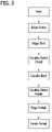
- FIG. 3depicts one embodiment of a wafer processing flow in accordance with the present disclosure.
- the waferis subjected to edge etching prior to double-sided grinding flatness treatment.
- edge etchingin accordance with embodiments of the present disclosure provides advantages over prior edge treatment methods, including edge polishing as shown in FIG. 2 .
- conventional edge polishing operationsgenerally require multi-step treatment of the wafer that increases wafer processing time and cost whereas the edge etching process of embodiments of the present disclosure is simpler and more economical than these conventional edge polishing operations.
- equipment and material costs of the edge etching methodare generally lower than those associated with conventional multi-stage edge polishing operations.
- the method of the present disclosureavoids excessive material costs as the entire wafer surface is not contacted with the etchant. Moreover, as noted elsewhere herein, the present method avoids the need for separation of stacked wafers upon completion of edge etching associated with various conventional edge etching operations that is often difficult and/or time-consuming. The edge etching methods disclosed herein may also reduce edge polishing times thus increasing throughput of the treatment process.
- An edge portion of a silicon wafer surface to be treated by the present methodis generally contacted with an etchant by immersing the edge portion of the wafer in the etchant.
- the waferis rotated to continuously contact an edge portion of the wafer by immersing the edge portion in a bath comprising the etchant.
- an edge portionmay be contacted with the etchant by rotating a wafer around an axis generally parallel to a top surface of the etchant or a bath comprising the etchant (e.g., around an axis generally parallel to the etchant or bath or at an angle ranging from 0° to 89°, with respect to a top surface of the etchant or bath).
- the waferis typically rotated about an axis oriented at an angle from about 0° to about 60°, from about 0° to about 40°, from about 0° to about 20°, or from about 0° to about 10° with respect to a top surface of the etchant.
- the processes of embodiments of the present disclosuregenerally employ as a starting material a silicon wafer that has been sliced from a single crystal silicon ingot and further processed, for example, using conventional grinding apparatus to profile and/or chamfer the peripheral edge of the wafer.
- This processingreduces the risk of wafer damage during further processing, reduces the non-uniform damage caused by the slicing process and roughly improves the general flatness and parallelism and flatness of the front and back surfaces.
- the wafermay be sliced from the ingot using any means known to persons skilled in the art, such as, for example, an internal diameter slicing apparatus or a wiresaw slicing apparatus. Wafer slicing and grinding processes are well-known to those skilled in the art.
- the silicon wafer starting materialmay have any conductivity type, resistivity, diameter, crystal orientation and target thickness appropriate for the intended semiconductor application.
- the wafer diameteris generally at least about 100 mm and may be about 150 mm, about 200 mm, about 300 mm, about 450 mm or greater, and the thickness of the wafer may be from about 475 ⁇ m to about 900 ⁇ m or greater, with the thickness typically increasing with increasing diameter.
- the radius of the wafermay be at least about 25 mm or at least about 50 mm, and even may be about 75 mm, about 100 mm, about 150 mm, about 225 mm or greater.
- the wafermay have any crystal orientation including, for example, ⁇ 100>, ⁇ 110>, and ⁇ 111> crystal orientations.
- the methods of embodiments of the present disclosurecomprise treating the peripheral edge and an edge portion of a silicon wafer by removing silicon from the peripheral edge and the edge portion of the wafer to provide a smooth edge surface.
- a point along the peripheral edge of the wafer nearest the central axisis defined by a notch.
- notch depthrefers to that point along the radius toward the central axis to which an orientation notch extends.
- an edge portion of the wafer contacted with the etchantis defined by the peripheral edge of the wafer and a point between the notch depth and the central axis (e.g., a point no more than about 15 mm from the peripheral edge, between about 1 mm and about 15 mm from the peripheral edge, or from the peripheral edge point nearest the central axis within any of the above-noted limits).
- silicon wafers treated by the present methodgenerally include a central axis X, a front surface 3 and a back surface 5 that are generally perpendicular to the central axis, and a radius (R) extending from the central axis to a point on the peripheral edge of the wafer.
- the waferalso includes a peripheral edge 7 and an edge portion 11 .
- the edge portionextends from the peripheral edge point 13 most near the edge 7 to a second point 15 that is more near the central axis than the peripheral edge point 13 .
- the pointsmay extend around the wafer to form a circle, and are depicted in FIG. 4 as dashed line circles.
- the wafers to be treatedalso generally include one or more flats or orientation notches 9 at the peripheral edge 7 of the wafer 1 .
- the peripheral edgemay include a plurality of flats, but generally includes one point along the peripheral edge of the wafer 1 nearest to the central axis X.
- the edge portion 11 of the wafer surface contacted with the etchantcorresponds to a portion of the wafer surface extending from the point along the peripheral edge nearest the central axis to a point between the nearest peripheral edge point and the central axis.
- the edge portionis defined by a point no more than about 15 mm from the nearest peripheral edge point.
- the edge portionis defined by a point no more than about 12 mm, no more than about 10 mm, no more than about 8 mm, or no more than about 6 mm from the nearest peripheral edge point (e.g., a point no more than about 5 mm, no more than about 4 mm, no more than about 3 mm, no more than about 2 mm, or no more than about 1 mm from the nearest peripheral edge point).
- the edge portion contacted with the etchantgenerally includes the peripheral edge of the wafer and a portion of the front surface and back surface of the wafer.
- the edge portion of the wafer surfaceis defined by a point between about 1 mm and about 15 mm from the nearest peripheral edge point, between about 1 mm and about 12 mm from the nearest peripheral edge point, or between about 1 mm and about 10 mm from the peripheral edge point.
- the edge portionis defined by a point between about 1 mm and about 8 mm from the nearest peripheral edge point, more typically between about 1 mm and about 6 mm from the nearest peripheral edge point and, more typically, between about 1 mm and about 5 mm from the nearest peripheral edge point (e.g., between about 1 mm and about 4 mm, between about 1 mm and about 3 mm, or between about 1 mm and about 2 mm from the nearest peripheral edge point).
- the edge 7 of the waferincludes two bevels 7 a and an apex 7 b intermediate the bevels.
- contact of an edge portion of the wafer surface with the etchantincludes contact of the peripheral edge and a portion of the front and/or back surface of the wafer.
- contact of a substantial portion of the wafer surfacee.g., total submersion of the wafer
- the radial distance to which the front surface and back surface are contacted with etchantare generally similar, but may vary based on processing conditions and apparatus limitations.
- Processes of embodiments of the present disclosureare generally conducted by immersing an edge portion of one or more wafers in a bath, or pool of etchant. Other processes are contemplated within the scope of this disclosure. Generally one or more wafers are positioned so that rotation of the wafer(s) immerses them in a pool, or bath, of etchant. As previously noted, conventional edge polishing typically involves a multi-step operation. Process of embodiments of the present disclosure is a single-step operation and may be easily incorporated into the overall silicon wafer processing operation including, for example, between wafer shaping operations (e.g., edge grinding) and caustic etching of the wafer surface as shown in FIG. 3 .
- wafer shaping operationse.g., edge grinding
- caustic etchingcaustic etching of the wafer surface as shown in FIG. 3 .
- the present processprovides a further benefit with respect to process efficiency since it is amenable to concurrent treatment of a plurality of wafers. More particularly, the present process may be easily adapted to treatment of edge portions of at least 2, at least 4, at least 5, at least 6, at least 8, at least 10, or more wafers. For example, the present process may be adapted to treatment of at least 10 wafers, at least 20 wafers, at least 30 wafers, at least 40 wafers, or at least 50 wafers.
- wafersundergo a light caustic etch immediately proceeding or immediately following the edge etch.
- the light caustic etchrelieves stress in the wafer and helps prevent any bowing or warp caused by the edge etch.
- the light etchmay remove from about 0.5 ⁇ m to about 2 ⁇ m and more typically from about 0.8 ⁇ m to about 1.2 ⁇ m of material from the surfaces of the wafer.
- the wafersundergo a double-sided grind following the edge etch to reduce the wafer flatness.
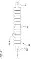
- FIGS. 6-9illustrate one embodiment of an edge etching apparatus or etcher 20 suitable for use in the processes of the present disclosure.
- the edge etcher 20generally includes a casing 25 .
- rollers 35that may support a number of wafers 45 .
- rollers 35may be located in various other arrangements besides that shown in FIG. 6 .
- the etcher 20may include more, or less, rollers 35 than depicted in FIG. 6 .
- the etchermay include one continuous section of rollers around an outer edge of the wafer 45 (e.g., rollers extending between the sections of rollers 35 shown in FIG. 6 ).
- a driving mechanism(not shown) drives rotation of the rollers 35 .
- the driving mechanismmay include a gear that rotates to drive each of the rollers of the edge etching apparatus.
- the gearmay be driven by, for example, an electric motor.
- the apparatus 20may also include top rollers 46 within the casing 25 .
- the top rollers 46help the wafer 45 to more precisely rotate about its axis.
- “top rollers”includes rollers positioned to engage wafers at a point on the uppermost 180 degrees of the wafer circumference.
- the top rollers 46may adjustably move up and down relative to the casing 25 such that the top rollers “float” above the wafers 45 .
- Weightsmay be attached to the top rollers 46 to assist the rollers in engaging and securing the wafers 45 .
- the upper rollers 46may be attached to a lid 60 that may open and shut as appropriate for loading and unloading of wafers.
- FIG. 7is a top view of the etching apparatus 20 without wafers loaded therein. Further, the etching apparatus 20 is illustrated without a lid and top rollers for purposes of illustration. As shown, each of the rollers 35 include grooves 40 that are generally in alignment with the grooves of adjacent rollers 35 . In this manner, multiple wafers in generally parallel alignment may be secured by the rollers.
- the casing 25may include an opening 50 . A valve (not shown) may be formed within the opening 50 to regulate the flow of etchant into and out of the casing 25 .
- FIG. 8is a top view of the etching apparatus 20 including a plurality of wafers 45 secured by the roller/groove arrangement shown in FIG. 7 .
- FIG. 9is a side view of the apparatus 20 illustrating the apparatus with a lid 60 open. The top rollers 46 are attached by suitable means to the lid 60 .
- wafersare added to the edge etching apparatus 20 such that the wafers are pinched between the grooves 40 of the rollers 35 .
- the lid 60is closed to seat the wafers 45 in the grooves of top rollers 46 .
- the edge etching apparatus 20may be immersed in a pool of etchant (not shown) to cause etchant to enter the etching apparatus through the opening 50 shown in FIG. 7 .
- etchantmay be introduced directly into the casing 25 through a second opening (not shown).
- the valve within the opening 50is closed to cause the etchant level to rise until etchant contacts the edge of the wafers 45 ( FIG. 6 ).
- the final etchant levelis designated by dashed line 52 .
- the depth of the reservoir of etchant in the etching apparatusis determined by the amount of etchant in the pool of etchant, the depth to which the etcher is immersed in the pool and/or the amount of etchant directly added into the casing 25 .
- the apparatus 20may also include an overflow hole (or “slot” or “weir”) (not shown) with the lowest point of the overflow hole defining the depth of etchant in the apparatus. In one embodiment, etchant that exits the overflow hole may be returned back to the apparatus 20 .
- the depth of etchant in the edge etching apparatus 20generally corresponds to the distance from the peripheral edge along the radius of the wafer to which the wafer is contacted with the etchant.
- rollers 35are driven by a central gear (not shown) to rotate the wafers and immerse the wafers in the pool, or bath, of etchant.
- the apparatus 20may be removed from the pool of etchant.
- the valve in the opening 50may be opened to cause etchant to exit or be expelled from the casing.
- the lid 60is opened and the wafers 45 may be removed from the etching apparatus 20 .
- FIG. 11depicts a roller 305 that may be used in the edge etching apparatus as depicted in FIGS. 6 - 9 and may also be used in various other embodiments.
- the roller 305 shown in FIG. 11includes a central axis X and includes a plurality of annular grooves 310 about the axis X.
- each roller 305includes ends 315 .
- a side view of an end 315is illustrated in FIG. 17 .
- FIG. 12shows the annular groove 310 of the roller 305 shown in FIG. 11 .
- the annular groove 310is defined by a first annular edge 311 and a second annular edge 312 . Both edges 311 , 312 extend radially inward towards the central axis of the roller. As can be seen from FIG. 12 , as the first and second annular edges 311 , 312 extend radially inward, the first annular edge and the second annular edge extend axially toward each other.
- the first annular edge 311has a most radially inward point 317 and the second annular edge 312 also includes a most radially inward point 319 .
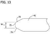
- FIG. 13illustrates an edge of a wafer 45 according to one embodiment of the present disclosure.
- the illustrated wafer edgeis known in the art as being “T-shaped” but other profiles including, for example, “R-shaped” profiles may be used without departing from the scope of the present disclosure.
- the edge 45includes an upper bevel 72 and a lower bevel 74 . Between the bevels 72 , 74 is an apex 75 .
- the apex 75defines a width W.
- the distance between the most radially inward point 317 and the most radially inward point 319 of the grove 310is less than an apex width W of the wafers that the grooves are sized and shaped to receive. As illustrated in FIG. 14 , this arrangement allows the wafer 45 to become pinched within the taper of the groove which allows the wafer 45 to more precisely rotate about its axis. A more precise rotation results in a smoother etch about the circumference of the wafer 45 .
- the distance between the most radially inward point 317 of the first edge 311 and the most radially inward point 319 of the second edge 312is less than an average thickness of the wafer.
- the distance between the most radially inward point 317 of the first edge 311 and the most radially inward point 319 of the second edge 312is less than 200 ⁇ m. In another embodiment, the distance is less than about 100 ⁇ m and, in other embodiments, from about 50 ⁇ m to about 200 ⁇ m or from about 50 ⁇ m to about 100 ⁇ m.
- a floor 333extends between the most radially inward point 317 of the first edge 311 and the most radially inward point 319 of the second edge 312 .
- the width of the floor 333may be less than an apex width W of the wafers that the grooves are sized and shaped to receive ( FIG. 14 ).
- the apex width W of the wafersmay be determined by use of an edge profiling inspection tool. Suitable equipment for edge profile inspecting include the LEP-2200 Edge Profile Monitor (Kobelco, Japan).
- the width of the flooris from about 50 ⁇ m and about 200 ⁇ m and, in another embodiment, from about 50 ⁇ m and about 100 ⁇ m.
- the groove 310may also include a third annular edge 319 and a fourth annular edge 320 .
- the groovedoes not include the third edge and fourth edge but rather only includes a first edge 311 ′ and second edge 312 ′.
- the first edge and the second edgeintersect to form a vertex point 315 ′′.
- the vertex point 315 ′′defines the most radially inward point of the first edge 311 ′′ and the most radially inward point of the second edge 312 ′′.
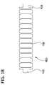
- FIG. 18illustrates a roller 405 that may be used in an edge etching apparatus as depicted in FIGS. 6-9 and in various other embodiments.
- the roller 405includes an end 415 that differs in design from the end 315 of FIG. 11 .
- the roller 405includes grooves 410 .
- the grooves 410may have the same configuration as any one of the grooves illustrated in FIGS. 14-16 .
- edge etchingmay be selected by one skilled in the art depending on the particular circumstances (e.g., the number of wafers to be treated and the desired characteristics of the edge-etched wafer(s)). For example, generally the one or more wafers are rotated at a rate that prevents etchant from flowing inward beyond the edge portion to the inner, or central portion of the wafer surface (e.g., at least about 10 revolutions per minute (rpm)), but generally below rates that may result in equipment damage and/or movement of wafers (e.g., speeds in excess of about 200 rpm).
- rpmrevolutions per minute
- the wafersare rotated at a rate of at least about 10 revolutions per minute (rpm), at least about 20 rpm, at least about 30 rpm, at least about 50 rpm, at least about 75 rpm or even at least about 90 rpm.
- the wafersare rotated at a rate of from about 10 rpm to about 60 rpm, from about 20 rpm to about 50 rpm, or from about 30 rpm to about 45 rpm.
- the wafersare rotated from about 75 rpm to about 125 rpm or from about 90 rpm to about 110 rpm.
- Other conditionsmay be used within the scope of this disclosure.
- the direction of rotation of the wafersmay be reversed such that the wafers are rotated in both clockwise and counter-clockwise directions while being contacting with etchant.
- the wafersare rotated in a clockwise direction for about 60 seconds at a speed of about 100 rpm and in a counter-clockwise direction for about 60 seconds at a speed of about 100 rpm.
- the time for which the edge portion is immersed in the etchantmay be selected in view of, for example, the starting edge surface roughness and/or the desired finished edge surface features.
- the peripheral edge and edge portions of the wafer surfaceare generally immersed in the etchant for at least about 30 seconds, at least about 1 minute, at least about 2 minutes, at least about 3 minutes, at least about 4 minutes, or at least about 5 minutes.
- the peripheral edge and edge portions of the waferare immersed in the etchant for no more than about 30 minutes, no more than about 20 minutes, or no more than about 10 minutes.
- the peripheral edge and edge portions of the wafermay be contacted with the etchant for a time of from about 1 minute to about 20 minutes, from about 1 minute to about 15 minutes, or from about 2 minutes to about 10 minutes.
- the amount of silicon removed from the peripheral edge and edge portions of the wafer surfacesvaries depending on the particular circumstances and conditions, but generally processes of embodiments of the present disclosure provide sufficient removal to provide a peripheral edge and edge portions that are sufficiently smooth in view of the fact that double-sided polishing does not address edge roughness.
- the peripheral edge and edge portions of the waferare immersed in the etchant for a time such that at least about 10 ⁇ m, at least about 20 ⁇ m, at least about 30 ⁇ m, at least about 40 ⁇ m, or at least about 50 ⁇ m of silicon, in terms of total thickness, is removed from the edge portions of the wafer surface.
- the peripheral edge and edge portions of the waferare immersed in the etchant for a time such that from about 10 to about 100 ⁇ m, more typically from about 20 to about 90 ⁇ m and, still more typically, from about 30 to about 80 ⁇ m (e.g., from about 40 to about 60 ⁇ m of silicon), in terms of total thickness is removed from the edge portion of the wafer surface.
- the peripheral edge and edge portions of the waferare immersed in the etchant for a time such that the diameter of the wafer is reduced by at least about 10 ⁇ m, at least about 20 ⁇ m, at least about 30 ⁇ m, at least about 40 ⁇ m, or at least about 50 ⁇ m.
- the peripheral edge and edge portions of the waferare immersed in the etchant for a time such that the diameter of the wafer is reduced by from about 10 to about 100 ⁇ m, more typically from about 20 to about 90 ⁇ m and, still more typically, from about 30 to about 80 ⁇ m.
- edge etching method of embodiments of the present disclosureis conducted prior to wafer flatness treatment (e.g., lapping or grinding). Accordingly, edge etching is typically conducted prior to reducing the flatness of the front and back surface of a wafer cut from a silicon ingot by at least about 50%, at least about 60%, at least about 70%, at least about 80% and, even more typically, at least about 90% (e.g., at least about 95%) as determined by the GBIR method.
- generally front and back surfaces of the wafer to be edge-etchedexhibit a total thickness variation of at least about 10 microns, typically at least about 20 microns and, more typically, at least about 25 microns.
- Edge etchingmay impact overall wafer flatness. Accordingly, the surfaces of edge-etched wafers typically exhibit total thickness variations in excess of 20 microns or in excess of about 25 microns (e.g., greater than about 30 microns, or greater than about 35 microns).
- Wafer treatment processes that are performed after the edge etchsuch as, for example, grinding, double-sided polishing and/or finish polishing
- the edge etchtypically reduce the flatness of the front surface of the wafer (as measured after being cut from the ingot and after the treatment process) by at about 50%, at least about 60%, at least about 70%, at least about 80% and, even, at least about 90% as determined by the GBIR method.
- the flatness of the back surface of the waferis reduced by the above-noted amounts.
- edge etching of the present methodis typically conducted prior to surface roughness treatment of the front and back surfaces of the wafer (e.g., acidic or caustic etching of the entire wafer surface).
- a portion of the front surface of edge-etched wafers and, particularly, the portions of the wafers not contacted with etchanti.e., a central potion of the surfaces that extends from the most radially inward point to which etchant contacts the wafer and the central axis
- the central portion of the front surface of the edge-etched waferexhibits surface roughness of from about 0.3 to about 2.5 ⁇ m Ra (from about 3 to about 25 ⁇ m Rt), from about 0.7 to about 2 ⁇ m Ra (from about 7 to about 20 ⁇ m Rt), or from about 1 to about 1.5 ⁇ m Ra (from about 10 to about 15 ⁇ m Rt).
- a portion of the back surface of edge-etched waferstypically exhibits an average surface roughness of at least about 0.3 ⁇ m Ra (at least about 3 ⁇ m Rt), at least about 1 ⁇ m Ra (at least about 10 ⁇ m Rt), or at least about 1.5 ⁇ m Ra (at least about 15 ⁇ m Rt).
- the central portion of the back surface of an edge-etched waferexhibits surface roughness of from about 0.3 to about 2.5 ⁇ m Ra (from about 3 to about 25 ⁇ m Rt), from about 0.7 to about 2 ⁇ m Ra (from about 7 to about 20 ⁇ m Rt), or from about 1 to about 1.5 ⁇ m Ra (from about 10 to about 15 ⁇ m Rt).
- edge etching in accordance with the present disclosuregenerally has little, if any effect on the roughness of these surfaces.
- the surface roughness of either or both of a front and back surfacechanges by no more than about 5%, no more than about 2%, and preferably no more than about 1% (e.g., no more than about 0.5%).
- edge surface roughness of edge-etched wafersis less than the overall front surface and back surface roughness.
- the surface roughness of an edge portion of edge-etched wafersis typically less than about 1 ⁇ m Ra, less than about 0.5 ⁇ m Ra, less than about 0.3 ⁇ m Ra, less than about 0.2 ⁇ m Ra, or less than about 0.1 ⁇ m Ra.
- edge surface roughness of edge-etched wafersis from about 0.05 to about 1 ⁇ m Ra, from about 0.1 to about 0.6 ⁇ m Ra, or from about 0.2 to about 0.5 ⁇ m Ra.
- the total thickness variation of the surfaces of the edge-etched waferis reduced (e.g., by grinding or lapping) to less than about 3 microns, less than about 2 microns, or less than about 1 micron.
- FIG. 10illustrates a wafer 200 prior to edge etching having an initial thickness T 0 defined by a front surface 205 and a back surface 210 .
- Wafer 200also includes a notch 215 extending from the peripheral edge of the wafer 220 to a notch depth 225 defining an edge portion P e of the wafer surface.
- Wafer 200also has an immersion region I extending from the peripheral edge 220 to a depth D that includes the edge portion P e of the wafer surface and a portion of the front surface 205 and back surface 210 of the wafer.
- FIG. 10also illustrates an edge-etched wafer 250 including an edge-etched region 255 that includes an etched notch portion 260 and an etched portion of the front surface 205 ′ and an etched portion of the back surface 210 ′.
- Contact with the etchantprovides silicon removal R from the front and back surface of the wafer for a total silicon removal from the immersion region of 2R and a final thickness of the immersion region of T f (T 0 ⁇ 2R).
- Acidic etchants suitable for edge etching in accordance with the present disclosureinclude those generally known in the art including, for example, those described in U.S. Pat. Nos. 3,964,957; 5,340,437; 5,211,794; 4,388,140; 5,236,548; 5,246,528; 4,971,645; 4,251,317; 4,849,701; 6,294,469; 5,233,218; 6,482,749; 6,046,117, the entire contents of which are incorporated herein by reference for all relevant purposes.
- the acidic etchantis in the form of an aqueous solution comprising a source of hydrogen ions.
- the source of hydrogen ionsmay be selected from the group consisting of hydrofluoric acid, nitric acid, phosphoric acid, acetic acid, sulfuric acid, hydrochloric acid, citric acid, oxalic acid, propionic acid, permanganic acid, and combinations thereof.
- the source of hydrogen ionsis present in the etchant at a concentration of at least about 40 wt %, more typically at least about 50 wt %, still more typically at least about 60 wt % and, even more typically, at least about 70 wt % (e.g., at least about 80 wt %, or at least about 90 wt %).
- the acidic etchantconsists essentially of water and the source of hydrogen ions.
- the acidic etchantcomprises one or more additives along with the source of hydrogen ions.
- the acidic etchantmay comprise a surfactant selected from the group consisting of ammonium fluoroalkylsulfonate (e.g., NovecTM 4300), potassium perfluorooctanesulfonate, dodecylbenzene sulfonic acid, alkyl aryl sulfonic acid, and combinations thereof.
- the acidic etchantmay comprise a fluorochemical surfactant (e.g., Fluorad® FC-95).
- the volumetric ratio of additive to source of hydrogen ionsis generally at least about 0.001:1, typically at least about 0.002:1 and, more typically, at least about 0.003:1.
- the volumetric ratio of additive to source of hydrogen ionsis from about 0.001 to about 1:1, from about 0.002:1 to about 0.5:1, or from about 0.003:1 to about 0.25:1.
- Caustic etchants suitable for edge etching in accordance with the present disclosureinclude those generally known in the art including, for example, those described in U.S. Pat. Nos. 7,323,421; 6,110,839; 6,383,060; and 6,503,363, the entire contents of which are incorporated herein by reference for all relevant purposes.
- the caustic etchantis in the form of an aqueous solution comprising a source of hydroxide ions.
- the source of hydroxide ionsgenerally comprises an alkali metal hydroxide selected from the group consisting of sodium hydroxide, potassium hydroxide, tetramethyl ammonium hydroxide, and combinations thereof.
- Edge portions of 15 P ⁇ 300 mm waferswere etched utilizing an edge etcher of the type shown in FIGS. 6-9 .
- the edge portionswere immersed in a pool of 300 ml of acidic etchant from the following mixture: 2.4 l of HNO 3 (69 wt. %), 2 l of H 3 PO 4 (85 wt %) and 0.55 l of HF (49 wt %).
- the etch time of the first, 7 wafer runwas 300 seconds, with rotation reversal after 150 seconds.
- Silicon removal, based on OGP diameter (a comparison of wafer diameter prior to and after etching)was approximately 30 ⁇ m.
- the etch time of the second, 8 wafer runwas 360 seconds, with rotation reversal after an etch time of 150 seconds.
- the tank containing the pool of etchantwas emptied and the wafers were rinsed with a spray of water for approximately 2 minutes to remove residual acid.
- the rinsed waferswere removed from the tank and dried. Wafers were then ground, double-sided polished, edge polished and evaluated for edge quality.
- 300 mm wafers ( 75 )were cut from a single crystal silicon ingot. After edge grinding, the edge portions of the wafers were etched utilizing an edge etcher of the type shown in FIGS. 6-9 .
- the waferswere split into a first group of 39 wafers and a second group of 36 wafers.
- the first group of waferswas edge polished (EP-300-X, SpeedFam) for 11 seconds and the second group was edge polished for 8 seconds.
- a third group ( 75 ) of waferswas cut from a single wafer and subjected to edge grinding and edge polishing (EP-300-X, SpeedFam).
- the edge polishwas a conventional 13 seconds in length.
- the edge etched waferswere then combined and double-sided polished.
- the wafers of the third groupwere also double-sided polished (AC-2000-P2, PeterWolters).
- the cassettes of all batches of waferswere combined and a finish polish was performed (LapMaster).
- the double-sided polishremoved approximately 15 ⁇ m of material from the wafer surfaces.
- the average diameter (OGP) of the edge etched waferswas 299.9946 mm after finish polishing and the average diameter (OGP) of the wafers that were not edge etched was 300.0211 mm after finish polishing. This corresponds to a 13.5 ⁇ m reduction in material from the wafer edge for edge etched wafers relative to edge polished wafers.
- the edge quality of the waferswas then determined by measuring the roughness by use of a Chapman profiler. The roughness was measured across the front bevel, back bevel and apex of the edge. The roughness was measured on three wafers from each batch at four points per wafer for a total of 12 points for each batch. The results were then averaged. The roughness measurements (Ra and RMS) are shown in Table 3.
Landscapes
- Engineering & Computer Science (AREA)
- Microelectronics & Electronic Packaging (AREA)
- Condensed Matter Physics & Semiconductors (AREA)
- General Physics & Mathematics (AREA)
- Manufacturing & Machinery (AREA)
- Computer Hardware Design (AREA)
- Physics & Mathematics (AREA)
- Power Engineering (AREA)
- Chemical & Material Sciences (AREA)
- Chemical Kinetics & Catalysis (AREA)
- General Chemical & Material Sciences (AREA)
- Weting (AREA)
- Mechanical Treatment Of Semiconductor (AREA)
Abstract
Description
- This application claims the benefit of U.S. Provisional Application No. 61/040,857, filed Mar. 31, 2008.
- The present disclosure generally relates to the manufacture of silicon wafers, and more particularly to apparatus and methods for etching the edge of a silicon wafer.
- Semiconductor wafers are generally prepared from a single crystal ingot (e.g., a silicon ingot) which is trimmed and ground to have one or more flats or notches for proper orientation of the wafer in subsequent procedures. The ingot is then sliced into individual wafers. The individual wafers are subjected to a number of processing operations to reduce the thickness of the wafer, remove damage caused by the slicing and/or other processing operations, and to create at least one highly reflective surface (e.g., on a front surface of the wafer).
- In addition to having at least one highly reflective surface, semiconductor wafers for advanced applications preferably have edges that are smooth, damage-free, and polished. Damaged edges may cause edge slip during thermal processing of the wafer. In addition, rough or pitted edges may trap particles that can be later released in a wet cleaning bath. The released particles may then undesirably migrate to the surface of the wafer. Furthermore, various films are deposited onto the wafer surface in some applications, which may deposit at the edge of the wafer. If the edge is not sufficiently smooth, residual film deposits at the edge may flake off. The flakes may come into contact with the surface of the wafer thereby causing surface defects. Conventional silicon wafer processing typically includes an edge treatment operation (e.g., polishing or etching) to provide edges that are sufficiently smooth.
- Prior to edge treatment, silicon wafers are typically subjected to a lapping or grinding operation to provide a wafer of the desired flatness, followed by an etching operation (acidic or caustic) to produce a wafer having desired surface roughness. After the flattening and etching operations, the wafers are typically subjected to a double-sided polishing operation to provide smooth front and back wafer surfaces.
- In edge polishing operations, wafer edges, including any orientation notch or flat, are typically polished by applying silica to a polishing pad or other surface that is pressed against the wafer edge. Generally, these polishing operations are carried out at a separate station and involve removing dry wafers from a process cassette, aligning the notches in the wafers, polishing the notch in the wafers, polishing the edge of the wafers, scrubbing and/or cleaning the wafers, spin drying the wafers, and then returning the dry wafers to the process cassette where the wafer can be moved to the next station. While edge polishing has proven effective, this operation increases processing time and cost.
- Edge etching operations typically include directing an etchant to the edge of the silicon wafer, typically to that portion of the surface extending from the peripheral edge to the flat portion of the wafer surface. Prevention of significant contact of the etchant with the flat portion of the wafer surface is addressed by various methods. These methods include supporting the wafer on a chuck and directing the etchant to the edge of the wafer surface. However, in these types of methods, it may be difficult to etch the peripheral edge of the wafer within the contour of a wafer notch. Various other methods involve stacking wafers together, often including gaskets between adjacent wafers, and directing the etchant to the exposed edge portion of the wafer. One disadvantage of these types of edge etching operations is difficulty in separating the wafers after etching.
- Recent advances in grinding technology provide flatter wafers with improved nanotopology, and the grinding surface depth has become more uniform and shallow. In addition, recent double-sided polishing operations offer the advantage of removal of small amounts of subsurface damage on both sides of the wafer. In fact, increased stock removal by double-sided polishing may increase the burden on the edge treatment (e.g., polishing) operation.
- Thus, there remains an unfulfilled need for a wafer edge treatment method that addresses the disadvantages of current edge treatment operations and is suitable for use in wafer processing operations utilizing recent developments in various aspects of wafer processing (e.g., grinding and/or double-sided polishing).
- Briefly, therefore, the present disclosure generally relates to a method for treating (e.g., etching) the edge of a silicon wafer.
- In particular, the present disclosure is directed to methods for removing silicon from a surface of a silicon wafer. The wafer comprises a central axis, a front surface and a back surface that are generally perpendicular to the central axis, a radius, R, extending from the central axis to a point along the peripheral edge of the wafer, a point along the peripheral edge of the wafer nearest the central axis, and edge portions of the front and back surfaces of the wafer. The edge portions extend from the nearest peripheral edge point to a point between the nearest peripheral edge point and the central axis and no more than about 15 mm from the nearest peripheral edge point. The method includes contacting with an etchant (i) the peripheral edge of the wafer, (ii) the edge portion of the front surface of the wafer, and (iii) the edge portion of the back surface of the wafer.
- In various embodiments, the contacting of the wafer with the etchant occurs prior to reducing the flatness of the wafer by more than about 50%.
- In other embodiments, the wafer has a total thickness variation of at least about 20 microns prior to contacting the wafer with the etchant.
- In various other embodiments, the method further comprises reducing the total thickness variation of the edge-etched wafer to less than about 3 microns.
- In still further embodiments, the edge portion of the front and back surfaces extend from the nearest peripheral edge point and a point between the nearest peripheral edge point and the central axis and between about 1 mm and about 15 mm from the nearest peripheral edge point.
- In even further embodiments, the method further comprises reducing the flatness of the edge-etched wafer by at least about 50%; contacting the peripheral edge, front surface, and back surface of the edge-etched wafer with a caustic etchant in the form of an aqueous solution comprising a source of hydroxide ions; polishing the front surface and back surface of the edge-etched wafer; and polishing the peripheral edge of the edge-etched wafer.
- The present disclosure is further directed to a silicon wafer comprising a central axis, a front surface and a back surface that are generally perpendicular to the central axis, a radius, R, extending from the central axis to a point along the peripheral edge, a point along the peripheral edge nearest the central axis, edge portions of the front and back surfaces of the wafer that extend from the nearest peripheral edge point to a point between the nearest peripheral point and the central axis and no more than about 15 mm from the nearest peripheral edge point, and central portions of the front and back surfaces of the wafer that extend from the point between the nearest peripheral point and the central axis and the central axis. The front and back surfaces of the wafer have a total thickness variation of at least 20 microns. The central portions of the front and back surfaces of the wafer have a surface roughness of at least about 0.3 μm Ra. The edge portions of the front and back surfaces of the wafer have a surface roughness of less than about 0.3 μm Ra.
- In another aspect of the present disclosure a silicon wafer comprises a central axis, a front surface and a back surface that are generally perpendicular to the central axis, a radius, R, extending from the central axis to a point along the peripheral edge, a point along the peripheral edge nearest the central axis, edge portions of the front and back surfaces of the wafer that extend from the nearest peripheral edge point to a point between the nearest peripheral point and the central axis, and central portions of the front and back surfaces of the wafer that extend from the point between the nearest peripheral point and the central axis and the central axis. The front and back surfaces of the wafer have a total thickness variation of at least 20 microns. The central portions of the front and back surfaces of the wafer have a surface roughness of at least about 0.3 μm Ra. The edge portions of the front and back surfaces of the wafer have a surface roughness of less than about 0.2 μm Ra.
- The present disclosure is also directed to an edge etching apparatus that comprises a casing and a plurality of rollers disposed within the casing. Each roller includes a central axis and a plurality of annular grooves in generally parallel alignment with the annular grooves of each adjacent roller.
FIGS. 1 and 2 are block diagrams illustrating processing steps in traditional wafer processing;FIG. 3 is a block diagram illustrating processing steps in a wafer processing method of one embodiment of the present disclosure;FIG. 4 is a perspective of a wafer that may be treated by the method of the present disclosure;FIG. 5 is a partial perspective of the wafer ofFIG. 4 with a portion of the wafer cut away;FIG. 6 is a side view of an edge etching apparatus according to one embodiment of the present disclosure;FIG. 7 is a top view of the edge etching apparatus ofFIG. 6 illustrating the apparatus without wafers;FIG. 8 is a top view of the edge etching apparatus ofFIG. 6 illustrating the apparatus with wafers loaded therein;FIG. 9 is a side view of the edge apparatus ofFIG. 6 illustrating the apparatus with a lid in an open position;FIG. 10 schematically illustrates surfaces and thicknesses of a silicon wafer prior to edge etching and after edge-etching;FIG. 11 is a side view of a roller of one embodiment of the present disclosure;FIG. 12 is an enlarged side view illustrating a groove of the roller ofFIG. 11 ;FIG. 13 is an enlarged side view of a wafer edge that may be treated by the method of the present disclosure;FIG. 14 is an enlarged side view illustrating a wafer engaged with the groove ofFIG. 12 ;FIG. 15 is an enlarged side view illustrating a wafer engaged with a groove according to a second embodiment of the present disclosure;FIG. 16 is an enlarged side view illustrating a wafer engaged with a groove according to a third embodiment of the present disclosure;FIG. 17 is an end view of the roller ofFIG. 11 ;FIG. 18 is a side view of a roller of a second embodiment of the present disclosure; andFIG. 19 is an end view of the roller ofFIG. 18 .- Corresponding reference characters indicate corresponding parts throughout the drawings.
- The present disclosure provides a method for treatment of an edge portion of a silicon wafer with an acidic or caustic etchant. In accordance with the present disclosure, the edge of the wafer is etched to remove wafer damage caused by prior treatment (e.g., edge grinding). In particular, the method of the present disclosure involves treating the edge of the wafer prior to any significant reduction in flatness of the wafer. For example, in various embodiments of the present disclosure the edge etching operation is conducted prior to a lapping or grinding operation (e.g., prior to reducing the flatness of the wafer by at least about 50% as measured by the GBIR method).
- In one embodiment, treating an edge portion of the wafer includes contacting a portion of the front and/or back surface of the wafer with the caustic etchant and, in another embodiment, with an acidic etchant. It should be noted that use of a caustic or an acidic etchant may degrade the flatness of the wafer edge and any other portion of the wafer surface contacted with the etchant. However, this potential negative of the edge etching operation may be addressed by conducting the edge etching operation prior to flatness treatment of the wafer, which is suitable for addressing any wafer flatness degradation caused by edge etching (e.g., double-sided polishing).
FIG. 1 depicts a traditional wafer processing flow. As shown, the surface of the wafer is etched (acidic or caustic) to remove mechanical damage to the wafer during wafer shaping operations (e.g., the wafer lapping and/or grinding operation), and to remove edge damage to the wafer caused during the edge grinding operation. Regardless of the particular etching operation, the etched wafer is typically subjected to an edge polishing operation, followed by a double-sided polishing operation. As noted, double-sided polishing operations generally do not treat the edge of the wafer surface.FIG. 2 depicts an additional example of conventional wafer processing flow in which a wafer is treated by a double-sided grinding operation, caustic etching, followed by edge polishing.FIG. 3 depicts one embodiment of a wafer processing flow in accordance with the present disclosure. As shown, the wafer is subjected to edge etching prior to double-sided grinding flatness treatment. As noted, wafer surface damage caused by edge etching is addressed by subsequent wafer treatment. In addition, edge etching in accordance with embodiments of the present disclosure provides advantages over prior edge treatment methods, including edge polishing as shown inFIG. 2 . Namely, as previously noted, conventional edge polishing operations generally require multi-step treatment of the wafer that increases wafer processing time and cost whereas the edge etching process of embodiments of the present disclosure is simpler and more economical than these conventional edge polishing operations. For example, equipment and material costs of the edge etching method are generally lower than those associated with conventional multi-stage edge polishing operations.- In addition, the method of the present disclosure avoids excessive material costs as the entire wafer surface is not contacted with the etchant. Moreover, as noted elsewhere herein, the present method avoids the need for separation of stacked wafers upon completion of edge etching associated with various conventional edge etching operations that is often difficult and/or time-consuming. The edge etching methods disclosed herein may also reduce edge polishing times thus increasing throughput of the treatment process.
- An edge portion of a silicon wafer surface to be treated by the present method is generally contacted with an etchant by immersing the edge portion of the wafer in the etchant. In various embodiments, the wafer is rotated to continuously contact an edge portion of the wafer by immersing the edge portion in a bath comprising the etchant. For example, an edge portion may be contacted with the etchant by rotating a wafer around an axis generally parallel to a top surface of the etchant or a bath comprising the etchant (e.g., around an axis generally parallel to the etchant or bath or at an angle ranging from 0° to 89°, with respect to a top surface of the etchant or bath). For example, the wafer is typically rotated about an axis oriented at an angle from about 0° to about 60°, from about 0° to about 40°, from about 0° to about 20°, or from about 0° to about 10° with respect to a top surface of the etchant.
- The processes of embodiments of the present disclosure generally employ as a starting material a silicon wafer that has been sliced from a single crystal silicon ingot and further processed, for example, using conventional grinding apparatus to profile and/or chamfer the peripheral edge of the wafer. This processing reduces the risk of wafer damage during further processing, reduces the non-uniform damage caused by the slicing process and roughly improves the general flatness and parallelism and flatness of the front and back surfaces. The wafer may be sliced from the ingot using any means known to persons skilled in the art, such as, for example, an internal diameter slicing apparatus or a wiresaw slicing apparatus. Wafer slicing and grinding processes are well-known to those skilled in the art.
- Regardless of the precise combination of prior processing, the silicon wafer starting material may have any conductivity type, resistivity, diameter, crystal orientation and target thickness appropriate for the intended semiconductor application. For example, the wafer diameter is generally at least about 100 mm and may be about 150 mm, about 200 mm, about 300 mm, about 450 mm or greater, and the thickness of the wafer may be from about 475 μm to about 900 μm or greater, with the thickness typically increasing with increasing diameter. Stated another way, the radius of the wafer may be at least about 25 mm or at least about 50 mm, and even may be about 75 mm, about 100 mm, about 150 mm, about 225 mm or greater. The wafer may have any crystal orientation including, for example, <100>, <110>, and <111> crystal orientations.
- Generally, the methods of embodiments of the present disclosure comprise treating the peripheral edge and an edge portion of a silicon wafer by removing silicon from the peripheral edge and the edge portion of the wafer to provide a smooth edge surface. Typically, a point along the peripheral edge of the wafer nearest the central axis is defined by a notch. As used herein, the term “notch depth” refers to that point along the radius toward the central axis to which an orientation notch extends. In accordance with these embodiments, an edge portion of the wafer contacted with the etchant is defined by the peripheral edge of the wafer and a point between the notch depth and the central axis (e.g., a point no more than about 15 mm from the peripheral edge, between about 1 mm and about 15 mm from the peripheral edge, or from the peripheral edge point nearest the central axis within any of the above-noted limits).
- Referring now to
FIG. 4 , silicon wafers treated by the present method generally include a central axis X, afront surface 3 and aback surface 5 that are generally perpendicular to the central axis, and a radius (R) extending from the central axis to a point on the peripheral edge of the wafer. The wafer also includes a peripheral edge7 and anedge portion 11. The edge portion extends from theperipheral edge point 13 most near the edge7 to asecond point 15 that is more near the central axis than theperipheral edge point 13. The points may extend around the wafer to form a circle, and are depicted inFIG. 4 as dashed line circles. - The wafers to be treated also generally include one or more flats or
orientation notches 9 at the peripheral edge7 of the wafer1. The peripheral edge may include a plurality of flats, but generally includes one point along the peripheral edge of the wafer1 nearest to the central axis X. Theedge portion 11 of the wafer surface contacted with the etchant corresponds to a portion of the wafer surface extending from the point along the peripheral edge nearest the central axis to a point between the nearest peripheral edge point and the central axis. Generally, the edge portion is defined by a point no more than about 15 mm from the nearest peripheral edge point. In various embodiments, the edge portion is defined by a point no more than about 12 mm, no more than about 10 mm, no more than about 8 mm, or no more than about 6 mm from the nearest peripheral edge point (e.g., a point no more than about 5 mm, no more than about 4 mm, no more than about 3 mm, no more than about 2 mm, or no more than about 1 mm from the nearest peripheral edge point). The edge portion contacted with the etchant generally includes the peripheral edge of the wafer and a portion of the front surface and back surface of the wafer. - In these and various other embodiments, the edge portion of the wafer surface is defined by a point between about 1 mm and about 15 mm from the nearest peripheral edge point, between about 1 mm and about 12 mm from the nearest peripheral edge point, or between about 1 mm and about 10 mm from the peripheral edge point. Typically, the edge portion is defined by a point between about 1 mm and about 8 mm from the nearest peripheral edge point, more typically between about 1 mm and about 6 mm from the nearest peripheral edge point and, more typically, between about 1 mm and about 5 mm from the nearest peripheral edge point (e.g., between about 1 mm and about 4 mm, between about 1 mm and about 3 mm, or between about 1 mm and about 2 mm from the nearest peripheral edge point).
- As shown in
FIG. 5 the edge7 of the wafer includes twobevels 7aand an apex7bintermediate the bevels. - As noted, contact of an edge portion of the wafer surface with the etchant includes contact of the peripheral edge and a portion of the front and/or back surface of the wafer. However, contact of a substantial portion of the wafer surface (e.g., total submersion of the wafer) is generally avoided to minimize unnecessary consumption of etchant. In this regard it is to be noted that the radial distance to which the front surface and back surface are contacted with etchant are generally similar, but may vary based on processing conditions and apparatus limitations.
- Processes of embodiments of the present disclosure are generally conducted by immersing an edge portion of one or more wafers in a bath, or pool of etchant. Other processes are contemplated within the scope of this disclosure. Generally one or more wafers are positioned so that rotation of the wafer(s) immerses them in a pool, or bath, of etchant. As previously noted, conventional edge polishing typically involves a multi-step operation. Process of embodiments of the present disclosure is a single-step operation and may be easily incorporated into the overall silicon wafer processing operation including, for example, between wafer shaping operations (e.g., edge grinding) and caustic etching of the wafer surface as shown in
FIG. 3 . It is to be further noted that the present process provides a further benefit with respect to process efficiency since it is amenable to concurrent treatment of a plurality of wafers. More particularly, the present process may be easily adapted to treatment of edge portions of at least 2, at least 4, at least 5, at least 6, at least 8, at least 10, or more wafers. For example, the present process may be adapted to treatment of at least 10 wafers, at least 20 wafers, at least 30 wafers, at least 40 wafers, or at least 50 wafers. - In one embodiment, wafers undergo a light caustic etch immediately proceeding or immediately following the edge etch. The light caustic etch relieves stress in the wafer and helps prevent any bowing or warp caused by the edge etch. The light etch may remove from about 0.5 μm to about 2 μm and more typically from about 0.8 μm to about 1.2 μm of material from the surfaces of the wafer. In another embodiment, the wafers undergo a double-sided grind following the edge etch to reduce the wafer flatness.
FIGS. 6-9 illustrate one embodiment of an edge etching apparatus oretcher 20 suitable for use in the processes of the present disclosure. As shown inFIG. 6 theedge etcher 20 generally includes acasing 25. Within thecasing 25 arerollers 35 that may support a number ofwafers 45. It is to be understood thatrollers 35 may be located in various other arrangements besides that shown inFIG. 6 . For example, theetcher 20 may include more, or less,rollers 35 than depicted inFIG. 6 . In addition, the etcher may include one continuous section of rollers around an outer edge of the wafer45 (e.g., rollers extending between the sections ofrollers 35 shown inFIG. 6 ). A driving mechanism (not shown) drives rotation of therollers 35. The driving mechanism may include a gear that rotates to drive each of the rollers of the edge etching apparatus. The gear may be driven by, for example, an electric motor.- The
apparatus 20 may also includetop rollers 46 within thecasing 25. Thetop rollers 46 help thewafer 45 to more precisely rotate about its axis. For purposes of the present disclosure, “top rollers” includes rollers positioned to engage wafers at a point on the uppermost 180 degrees of the wafer circumference. Thetop rollers 46 may adjustably move up and down relative to thecasing 25 such that the top rollers “float” above thewafers 45. Weights may be attached to thetop rollers 46 to assist the rollers in engaging and securing thewafers 45. Theupper rollers 46 may be attached to alid 60 that may open and shut as appropriate for loading and unloading of wafers. FIG. 7 is a top view of theetching apparatus 20 without wafers loaded therein. Further, theetching apparatus 20 is illustrated without a lid and top rollers for purposes of illustration. As shown, each of therollers 35 includegrooves 40 that are generally in alignment with the grooves ofadjacent rollers 35. In this manner, multiple wafers in generally parallel alignment may be secured by the rollers. Thecasing 25 may include anopening 50. A valve (not shown) may be formed within theopening 50 to regulate the flow of etchant into and out of thecasing 25.FIG. 8 is a top view of theetching apparatus 20 including a plurality ofwafers 45 secured by the roller/groove arrangement shown inFIG. 7 .FIG. 9 is a side view of theapparatus 20 illustrating the apparatus with alid 60 open. Thetop rollers 46 are attached by suitable means to thelid 60.- In conventional apparatus, one must separate each wafer after etching from a stack of wafers. This process can be labor-intensive, difficult and time consuming. Use of the
etching apparatus 20 as depicted inFIGS. 6-9 eliminates this separation step. - In one embodiment of a method of this disclosure, wafers are added to the
edge etching apparatus 20 such that the wafers are pinched between thegrooves 40 of therollers 35. Thelid 60 is closed to seat thewafers 45 in the grooves oftop rollers 46. For contact of thewafers 45 with the etchant, theedge etching apparatus 20 may be immersed in a pool of etchant (not shown) to cause etchant to enter the etching apparatus through theopening 50 shown inFIG. 7 . Alternatively, etchant may be introduced directly into thecasing 25 through a second opening (not shown). The valve within theopening 50 is closed to cause the etchant level to rise until etchant contacts the edge of the wafers45 (FIG. 6 ). The final etchant level is designated by dashedline 52. - The depth of the reservoir of etchant in the etching apparatus is determined by the amount of etchant in the pool of etchant, the depth to which the etcher is immersed in the pool and/or the amount of etchant directly added into the
casing 25. Theapparatus 20 may also include an overflow hole (or “slot” or “weir”) (not shown) with the lowest point of the overflow hole defining the depth of etchant in the apparatus. In one embodiment, etchant that exits the overflow hole may be returned back to theapparatus 20. - The depth of etchant in the
edge etching apparatus 20 generally corresponds to the distance from the peripheral edge along the radius of the wafer to which the wafer is contacted with the etchant. - Once the etcher is immersed in the etchant, the
rollers 35 are driven by a central gear (not shown) to rotate the wafers and immerse the wafers in the pool, or bath, of etchant. - After etching, the
apparatus 20 may be removed from the pool of etchant. In embodiments, where etchant is added directly to thecasing 25, the valve in theopening 50 may be opened to cause etchant to exit or be expelled from the casing. Thelid 60 is opened and thewafers 45 may be removed from theetching apparatus 20. FIG. 11 depicts aroller 305 that may be used in the edge etching apparatus as depicted in FIGS.6-9 and may also be used in various other embodiments. Theroller 305 shown inFIG. 11 includes a central axis X and includes a plurality ofannular grooves 310 about the axis X. As shown inFIG. 11 , eachroller 305 includes ends315. A side view of anend 315 is illustrated inFIG. 17 .FIG. 12 shows theannular groove 310 of theroller 305 shown inFIG. 11 . Theannular groove 310 is defined by a firstannular edge 311 and a secondannular edge 312. Both edges311,312 extend radially inward towards the central axis of the roller. As can be seen fromFIG. 12 , as the first and secondannular edges annular edge 311 has a most radiallyinward point 317 and the secondannular edge 312 also includes a most radiallyinward point 319.FIG. 13 illustrates an edge of awafer 45 according to one embodiment of the present disclosure. The illustrated wafer edge is known in the art as being “T-shaped” but other profiles including, for example, “R-shaped” profiles may be used without departing from the scope of the present disclosure. Theedge 45 includes anupper bevel 72 and alower bevel 74. Between thebevels - In one embodiment, the distance between the most radially
inward point 317 and the most radiallyinward point 319 of thegrove 310 is less than an apex width W of the wafers that the grooves are sized and shaped to receive. As illustrated inFIG. 14 , this arrangement allows thewafer 45 to become pinched within the taper of the groove which allows thewafer 45 to more precisely rotate about its axis. A more precise rotation results in a smoother etch about the circumference of thewafer 45. - In another embodiment, the distance between the most radially
inward point 317 of thefirst edge 311 and the most radiallyinward point 319 of thesecond edge 312 is less than an average thickness of the wafer. - In one embodiment, the distance between the most radially
inward point 317 of thefirst edge 311 and the most radiallyinward point 319 of thesecond edge 312 is less than 200 μm. In another embodiment, the distance is less than about 100 μm and, in other embodiments, from about 50 μm to about 200 μm or from about 50 μm to about 100 μm. - As illustrated in
FIG. 12 , afloor 333 extends between the most radiallyinward point 317 of thefirst edge 311 and the most radiallyinward point 319 of thesecond edge 312. The width of thefloor 333 may be less than an apex width W of the wafers that the grooves are sized and shaped to receive (FIG. 14 ). The apex width W of the wafers may be determined by use of an edge profiling inspection tool. Suitable equipment for edge profile inspecting include the LEP-2200 Edge Profile Monitor (Kobelco, Japan). - In one embodiment, the width of the floor is from about 50 μm and about 200 μm and, in another embodiment, from about 50 μm and about 100 μm.
- The
groove 310 may also include a thirdannular edge 319 and a fourthannular edge 320. In one embodiment and as illustrated inFIG. 15 , the groove does not include the third edge and fourth edge but rather only includes afirst edge 311′ andsecond edge 312′. - Referring now to
FIG. 16 , in one embodiment, the first edge and the second edge intersect to form avertex point 315″. Thevertex point 315″ defines the most radially inward point of thefirst edge 311″ and the most radially inward point of thesecond edge 312″. FIG. 18 illustrates aroller 405 that may be used in an edge etching apparatus as depicted inFIGS. 6-9 and in various other embodiments. Theroller 405 includes anend 415 that differs in design from theend 315 ofFIG. 11 . Theroller 405 includesgrooves 410. Thegrooves 410 may have the same configuration as any one of the grooves illustrated inFIGS. 14-16 .- The conditions of edge etching may be selected by one skilled in the art depending on the particular circumstances (e.g., the number of wafers to be treated and the desired characteristics of the edge-etched wafer(s)). For example, generally the one or more wafers are rotated at a rate that prevents etchant from flowing inward beyond the edge portion to the inner, or central portion of the wafer surface (e.g., at least about 10 revolutions per minute (rpm)), but generally below rates that may result in equipment damage and/or movement of wafers (e.g., speeds in excess of about 200 rpm). Thus, generally the wafers are rotated at a rate of at least about 10 revolutions per minute (rpm), at least about 20 rpm, at least about 30 rpm, at least about 50 rpm, at least about 75 rpm or even at least about 90 rpm. Typically, the wafers are rotated at a rate of from about 10 rpm to about 60 rpm, from about 20 rpm to about 50 rpm, or from about 30 rpm to about 45 rpm. In other embodiments the wafers are rotated from about 75 rpm to about 125 rpm or from about 90 rpm to about 110 rpm. Other conditions may be used within the scope of this disclosure.
- In one embodiment, the direction of rotation of the wafers may be reversed such that the wafers are rotated in both clockwise and counter-clockwise directions while being contacting with etchant. In one embodiment, the wafers are rotated in a clockwise direction for about 60 seconds at a speed of about 100 rpm and in a counter-clockwise direction for about 60 seconds at a speed of about 100 rpm.
- The time for which the edge portion is immersed in the etchant may be selected in view of, for example, the starting edge surface roughness and/or the desired finished edge surface features. Regardless of the particular circumstances, the peripheral edge and edge portions of the wafer surface are generally immersed in the etchant for at least about 30 seconds, at least about 1 minute, at least about 2 minutes, at least about 3 minutes, at least about 4 minutes, or at least about 5 minutes. In accordance with these and various other embodiments, the peripheral edge and edge portions of the wafer are immersed in the etchant for no more than about 30 minutes, no more than about 20 minutes, or no more than about 10 minutes. For example, the peripheral edge and edge portions of the wafer may be contacted with the etchant for a time of from about 1 minute to about 20 minutes, from about 1 minute to about 15 minutes, or from about 2 minutes to about 10 minutes.
- The amount of silicon removed from the peripheral edge and edge portions of the wafer surfaces varies depending on the particular circumstances and conditions, but generally processes of embodiments of the present disclosure provide sufficient removal to provide a peripheral edge and edge portions that are sufficiently smooth in view of the fact that double-sided polishing does not address edge roughness. Generally, the peripheral edge and edge portions of the wafer are immersed in the etchant for a time such that at least about 10 μm, at least about 20 μm, at least about 30 μm, at least about 40 μm, or at least about 50 μm of silicon, in terms of total thickness, is removed from the edge portions of the wafer surface. Typically, the peripheral edge and edge portions of the wafer are immersed in the etchant for a time such that from about 10 to about 100 μm, more typically from about 20 to about 90 μm and, still more typically, from about 30 to about 80 μm (e.g., from about 40 to about 60 μm of silicon), in terms of total thickness is removed from the edge portion of the wafer surface.
- In one embodiment, the peripheral edge and edge portions of the wafer are immersed in the etchant for a time such that the diameter of the wafer is reduced by at least about 10 μm, at least about 20 μm, at least about 30 μm, at least about 40 μm, or at least about 50 μm. Typically, the peripheral edge and edge portions of the wafer are immersed in the etchant for a time such that the diameter of the wafer is reduced by from about 10 to about 100 μm, more typically from about 20 to about 90 μm and, still more typically, from about 30 to about 80 μm.
- As noted elsewhere herein and depicted in
FIG. 3 , the edge etching method of embodiments of the present disclosure is conducted prior to wafer flatness treatment (e.g., lapping or grinding). Accordingly, edge etching is typically conducted prior to reducing the flatness of the front and back surface of a wafer cut from a silicon ingot by at least about 50%, at least about 60%, at least about 70%, at least about 80% and, even more typically, at least about 90% (e.g., at least about 95%) as determined by the GBIR method. Thus, generally front and back surfaces of the wafer to be edge-etched exhibit a total thickness variation of at least about 10 microns, typically at least about 20 microns and, more typically, at least about 25 microns. Edge etching may impact overall wafer flatness. Accordingly, the surfaces of edge-etched wafers typically exhibit total thickness variations in excess of 20 microns or in excess of about 25 microns (e.g., greater than about 30 microns, or greater than about 35 microns). - Wafer treatment processes that are performed after the edge etch such as, for example, grinding, double-sided polishing and/or finish polishing) typically reduce the flatness of the front surface of the wafer (as measured after being cut from the ingot and after the treatment process) by at about 50%, at least about 60%, at least about 70%, at least about 80% and, even, at least about 90% as determined by the GBIR method. In other embodiments, the flatness of the back surface of the wafer is reduced by the above-noted amounts.
- Also shown in
FIG. 3 , edge etching of the present method is typically conducted prior to surface roughness treatment of the front and back surfaces of the wafer (e.g., acidic or caustic etching of the entire wafer surface). Accordingly, a portion of the front surface of edge-etched wafers and, particularly, the portions of the wafers not contacted with etchant (i.e., a central potion of the surfaces that extends from the most radially inward point to which etchant contacts the wafer and the central axis), will typically exhibit an average surface roughness of at least about 0.3 μm Ra (at least about 3 μm Rt), at least about 1 μm Ra (at least about 10 μm Rt), or at least about 1.5 μm Ra (at least about 15 μm Rt). Typically, the central portion of the front surface of the edge-etched wafer exhibits surface roughness of from about 0.3 to about 2.5 μm Ra (from about 3 to about 25 μm Rt), from about 0.7 to about 2 μm Ra (from about 7 to about 20 μm Rt), or from about 1 to about 1.5 μm Ra (from about 10 to about 15 μm Rt). - Additionally or alternatively, a portion of the back surface of edge-etched wafers (i.e., the corresponding central portion of the back surface of the wafer) typically exhibits an average surface roughness of at least about 0.3 μm Ra (at least about 3 μm Rt), at least about 1 μm Ra (at least about 10 μm Rt), or at least about 1.5 μm Ra (at least about 15 μm Rt). Typically, the central portion of the back surface of an edge-etched wafer exhibits surface roughness of from about 0.3 to about 2.5 μm Ra (from about 3 to about 25 μm Rt), from about 0.7 to about 2 μm Ra (from about 7 to about 20 μm Rt), or from about 1 to about 1.5 μm Ra (from about 10 to about 15 μm Rt). Regardless of the initial surface roughness of a portion of the front and/or back surface it is to be noted that edge etching in accordance with the present disclosure generally has little, if any effect on the roughness of these surfaces. For example, typically the surface roughness of either or both of a front and back surface changes by no more than about 5%, no more than about 2%, and preferably no more than about 1% (e.g., no more than about 0.5%).
- Since edge etching removes edge damage, the edge surface roughness of edge-etched wafers is less than the overall front surface and back surface roughness. For example, the surface roughness of an edge portion of edge-etched wafers is typically less than about 1 μm Ra, less than about 0.5 μm Ra, less than about 0.3 μm Ra, less than about 0.2 μm Ra, or less than about 0.1 μm Ra. Typically, edge surface roughness of edge-etched wafers is from about 0.05 to about 1 μm Ra, from about 0.1 to about 0.6 μm Ra, or from about 0.2 to about 0.5 μm Ra.
- In various embodiments, after edge etching is complete, typically the total thickness variation of the surfaces of the edge-etched wafer is reduced (e.g., by grinding or lapping) to less than about 3 microns, less than about 2 microns, or less than about 1 micron.
FIG. 10 illustrates awafer 200 prior to edge etching having an initial thickness T0defined by afront surface 205 and aback surface 210.Wafer 200 also includes anotch 215 extending from the peripheral edge of thewafer 220 to anotch depth 225 defining an edge portion Peof the wafer surface.Wafer 200 also has an immersion region I extending from theperipheral edge 220 to a depth D that includes the edge portion Peof the wafer surface and a portion of thefront surface 205 andback surface 210 of the wafer.FIG. 10 also illustrates an edge-etchedwafer 250 including an edge-etchedregion 255 that includes an etchednotch portion 260 and an etched portion of thefront surface 205′ and an etched portion of theback surface 210′. Contact with the etchant provides silicon removal R from the front and back surface of the wafer for a total silicon removal from the immersion region of 2R and a final thickness of the immersion region of Tf(T0−2R).- Acidic etchants suitable for edge etching in accordance with the present disclosure include those generally known in the art including, for example, those described in U.S. Pat. Nos. 3,964,957; 5,340,437; 5,211,794; 4,388,140; 5,236,548; 5,246,528; 4,971,645; 4,251,317; 4,849,701; 6,294,469; 5,233,218; 6,482,749; 6,046,117, the entire contents of which are incorporated herein by reference for all relevant purposes. Generally, the acidic etchant is in the form of an aqueous solution comprising a source of hydrogen ions. The source of hydrogen ions may be selected from the group consisting of hydrofluoric acid, nitric acid, phosphoric acid, acetic acid, sulfuric acid, hydrochloric acid, citric acid, oxalic acid, propionic acid, permanganic acid, and combinations thereof. Typically, the source of hydrogen ions is present in the etchant at a concentration of at least about 40 wt %, more typically at least about 50 wt %, still more typically at least about 60 wt % and, even more typically, at least about 70 wt % (e.g., at least about 80 wt %, or at least about 90 wt %).
- In various embodiments, the acidic etchant consists essentially of water and the source of hydrogen ions. In various other embodiments, the acidic etchant comprises one or more additives along with the source of hydrogen ions. For example, the acidic etchant may comprise a surfactant selected from the group consisting of ammonium fluoroalkylsulfonate (e.g., Novec™ 4300), potassium perfluorooctanesulfonate, dodecylbenzene sulfonic acid, alkyl aryl sulfonic acid, and combinations thereof. In various embodiments the acidic etchant may comprise a fluorochemical surfactant (e.g., Fluorad® FC-95). Whether a surfactant is the lone additive, or other additives are included in the etchant, the volumetric ratio of additive to source of hydrogen ions is generally at least about 0.001:1, typically at least about 0.002:1 and, more typically, at least about 0.003:1. For example, in various embodiments the volumetric ratio of additive to source of hydrogen ions is from about 0.001 to about 1:1, from about 0.002:1 to about 0.5:1, or from about 0.003:1 to about 0.25:1.
- Caustic etchants suitable for edge etching in accordance with the present disclosure include those generally known in the art including, for example, those described in U.S. Pat. Nos. 7,323,421; 6,110,839; 6,383,060; and 6,503,363, the entire contents of which are incorporated herein by reference for all relevant purposes. Generally, the caustic etchant is in the form of an aqueous solution comprising a source of hydroxide ions. The source of hydroxide ions generally comprises an alkali metal hydroxide selected from the group consisting of sodium hydroxide, potassium hydroxide, tetramethyl ammonium hydroxide, and combinations thereof.
- Edge portions of 15 P− 300 mm wafers were etched utilizing an edge etcher of the type shown in
FIGS. 6-9 . The edge portions were immersed in a pool of 300 ml of acidic etchant from the following mixture: 2.4 l of HNO3(69 wt. %), 2 l of H3PO4(85 wt %) and 0.55 l of HF (49 wt %). - Two runs were carried out, one in which an edge portion of 7 wafers were etched with the edge portion extended from the nearest peripheral edge point to a point approximately 8.5 mm from the nearest peripheral edge point. In the second run 8 wafers were etched with the edge portion extending to a point approximately 8.5 mm from the nearest peripheral edge point.
- The etch time of the first, 7 wafer run was 300 seconds, with rotation reversal after 150 seconds. Silicon removal, based on OGP diameter (a comparison of wafer diameter prior to and after etching) was approximately 30 μm.
- The etch time of the second, 8 wafer run was 360 seconds, with rotation reversal after an etch time of 150 seconds. Silicon removal, based on OGP diameter, was also approximately 30 μm.
- Both runs were conducted at a wafer spin speed of from 25 to 30 rpm.
- At the end of each etching cycle, the tank containing the pool of etchant was emptied and the wafers were rinsed with a spray of water for approximately 2 minutes to remove residual acid. The rinsed wafers were removed from the tank and dried. Wafers were then ground, double-sided polished, edge polished and evaluated for edge quality.
- Edge quality, as measured by Chapman roughness was comparable to standard product. Edge measurements showed little residual damage.
- 300 mm wafers (75) were cut from a single crystal silicon ingot. After edge grinding, the edge portions of the wafers were etched utilizing an edge etcher of the type shown in
FIGS. 6-9 . - The wafers were split into a first group of 39 wafers and a second group of 36 wafers. The first group of wafers was edge polished (EP-300-X, SpeedFam) for 11 seconds and the second group was edge polished for 8 seconds.
- A third group (75) of wafers was cut from a single wafer and subjected to edge grinding and edge polishing (EP-300-X, SpeedFam). The edge polish was a conventional 13 seconds in length.
- The edge etched wafers were then combined and double-sided polished. The wafers of the third group were also double-sided polished (AC-2000-P2, PeterWolters). The cassettes of all batches of wafers were combined and a finish polish was performed (LapMaster). The double-sided polish removed approximately 15 μm of material from the wafer surfaces.
- The average diameter (OGP) of the edge etched wafers was 299.9946 mm after finish polishing and the average diameter (OGP) of the wafers that were not edge etched was 300.0211 mm after finish polishing. This corresponds to a 13.5 μm reduction in material from the wafer edge for edge etched wafers relative to edge polished wafers.
- The flatness of the three batches of wafers of Example 2 was determined by both GBIR, SBIR and SFQR methods after finish polishing. The results are shown in Table 1 below.
TABLE 1 Flatness data for edge etched wafers and non-edge etched wafers after double-sided polishing and finish polishing Average Average Average SBIR Max SFQR Max Non-Edge Etched (13 sec) 308.7 118.7 29.8 Edge Etched (11 sec) 315.9 124.5 41.3 Edge Etched (8 sec) 299.8 108.5 37.0
As can be seen from Table 1, edge etching did not significantly degrade the flatness of finish polished wafers.- The edge quality of the wafers was then tested on a Raytex edge inspection system (Raytex-300) the system outputs were averaged for each group. The results of the analysis are shown in Table 2 below.
TABLE 2 Raytex measurements for edge etched and non-edge etched wafers after finish polishing Average DC Average AC Non-Edge Etched (13 sec) 488.3 145.3 Edge Etched (11 sec) 492.2 133.6 Edge Etched (8 sec) 491.7 130.1
As can be seen from Table 2, the DC output (which is indicative of the amount of pits/chips/bumps) was only slightly worse for etched wafers and the AC output for edge etched wafers (indicative of a smooth surface finish) was better than non-edge etched wafers.- The edge quality of the wafers was then determined by measuring the roughness by use of a Chapman profiler. The roughness was measured across the front bevel, back bevel and apex of the edge. The roughness was measured on three wafers from each batch at four points per wafer for a total of 12 points for each batch. The results were then averaged. The roughness measurements (Ra and RMS) are shown in Table 3.
TABLE 3 Ra and RMS edge roughness for edge etched wafers and non- edge etched wafers Front Front Back Back Bevel Ra Bevel RMS Bevel Ra Bevel RMS Apex Ra Apex RMS (average) (average) (average) (average) (average) (average) Non-Edge 4.95 6.22 5.18 6.56 11.56 14.51 Etched (13 sec) Edge Etched 5.22 6.47 5.10 6.46 10.35 12.89 (11 sec) Edge Etched (8 sec) 5.47 7.10 4.76 5.97 11.10 13.91
As can be seen from Table 3, edge etching does not significantly increase the roughness of the edge of the wafer.- The present disclosure is not limited to the above embodiments and can be variously modified. The above description of the embodiments, including the Examples, is intended only to acquaint others skilled in the art with the disclosure, its principles, and its practical application so that others skilled in the art may adapt and apply the disclosure in its numerous forms, as may be best suited to the requirements of a particular use.
- With reference to the use of the word(s) comprise or comprises or comprising in this entire specification (including the claims below), unless the context requires otherwise, those words are used on the basis and clear understanding that they are to be interpreted inclusively, rather than exclusively, and applicants intend each of those words to be so interpreted in construing this entire specification.
- When introducing elements of the present disclosure or the embodiment(s) thereof, the articles “a”, “an”, “the” and “said” are intended to mean that there are one or more of the elements. The terms “comprising”, “including” and “having” are intended to be inclusive and mean that there may be additional elements other than the listed elements.
- In view of the above, it will be seen that the several objects of the disclosure are achieved and other advantageous results attained.
Claims (16)
Priority Applications (1)
| Application Number | Priority Date | Filing Date | Title |
|---|---|---|---|
| US12/415,274US20090242126A1 (en) | 2008-03-31 | 2009-03-31 | Edge etching apparatus for etching the edge of a silicon wafer |
Applications Claiming Priority (2)
| Application Number | Priority Date | Filing Date | Title |
|---|---|---|---|
| US4085708P | 2008-03-31 | 2008-03-31 | |
| US12/415,274US20090242126A1 (en) | 2008-03-31 | 2009-03-31 | Edge etching apparatus for etching the edge of a silicon wafer |
Publications (1)
| Publication Number | Publication Date |
|---|---|
| US20090242126A1true US20090242126A1 (en) | 2009-10-01 |
Family
ID=40676112
Family Applications (3)
| Application Number | Title | Priority Date | Filing Date |
|---|---|---|---|
| US12/415,551Active2031-01-18US8309464B2 (en) | 2008-03-31 | 2009-03-31 | Methods for etching the edge of a silicon wafer |
| US12/415,555Active2030-04-13US8192822B2 (en) | 2008-03-31 | 2009-03-31 | Edge etched silicon wafers |
| US12/415,274AbandonedUS20090242126A1 (en) | 2008-03-31 | 2009-03-31 | Edge etching apparatus for etching the edge of a silicon wafer |
Family Applications Before (2)
| Application Number | Title | Priority Date | Filing Date |
|---|---|---|---|
| US12/415,551Active2031-01-18US8309464B2 (en) | 2008-03-31 | 2009-03-31 | Methods for etching the edge of a silicon wafer |
| US12/415,555Active2030-04-13US8192822B2 (en) | 2008-03-31 | 2009-03-31 | Edge etched silicon wafers |
Country Status (7)
| Country | Link |
|---|---|
| US (3) | US8309464B2 (en) |
| EP (1) | EP2260507B1 (en) |
| JP (1) | JP5478604B2 (en) |
| KR (1) | KR20110008068A (en) |
| CN (1) | CN101981664B (en) |
| TW (1) | TWI430348B (en) |
| WO (1) | WO2009124060A1 (en) |
Cited By (7)
| Publication number | Priority date | Publication date | Assignee | Title |
|---|---|---|---|---|
| US20090246444A1 (en)* | 2008-03-31 | 2009-10-01 | Memc Electronic Materials, Inc. | Edge etched silicon wafers |
| US20110223741A1 (en)* | 2008-11-19 | 2011-09-15 | Memc Electronic Materials, Inc. | Method and system for stripping the edge of a semiconductor wafer |
| CN102569502A (en)* | 2011-12-16 | 2012-07-11 | 合肥晶澳太阳能科技有限公司 | Wet method etching process |
| US20120175343A1 (en)* | 2011-01-12 | 2012-07-12 | Siltronic Corporation | Apparatus and method for etching a wafer edge |
| US20130069057A1 (en)* | 2011-09-21 | 2013-03-21 | Jer-Liang Yeh | Wafer with high rupture resistance |
| US8853054B2 (en) | 2012-03-06 | 2014-10-07 | Sunedison Semiconductor Limited | Method of manufacturing silicon-on-insulator wafers |
| CN104701241A (en)* | 2013-12-05 | 2015-06-10 | 中芯国际集成电路制造(上海)有限公司 | Semiconductor component edge etching method |
Families Citing this family (18)
| Publication number | Priority date | Publication date | Assignee | Title |
|---|---|---|---|---|
| JP5644401B2 (en)* | 2010-11-15 | 2014-12-24 | 株式会社Sumco | Epitaxial wafer manufacturing method and epitaxial wafer |
| KR20120136881A (en)* | 2011-06-10 | 2012-12-20 | 동우 화인켐 주식회사 | Texture etching solution composition and texture etching method of crystalline silicon wafers |
| JP6100002B2 (en)* | 2013-02-01 | 2017-03-22 | 株式会社荏原製作所 | Substrate back surface polishing method and substrate processing apparatus |
| JP6071611B2 (en)* | 2013-02-13 | 2017-02-01 | Mipox株式会社 | Method for manufacturing circular wafer by polishing peripheral edge of wafer made of crystalline material having notch portion such as orientation flat using polishing tape |
| US20150060401A1 (en)* | 2013-08-29 | 2015-03-05 | Corning Incorporated | Method of edge coating a batch of glass articles |
| JP6223873B2 (en)* | 2014-03-14 | 2017-11-01 | 株式会社荏原製作所 | Polishing apparatus and polishing method |
| US20150371956A1 (en)* | 2014-06-19 | 2015-12-24 | Globalfoundries Inc. | Crackstops for bulk semiconductor wafers |
| CN104465324A (en)* | 2014-11-28 | 2015-03-25 | 上海芯亮电子科技有限公司 | Discrete component manufacturing method |
| DE102015220924B4 (en)* | 2015-10-27 | 2018-09-27 | Siltronic Ag | Susceptor for holding a semiconductor wafer with orientation notch, method for depositing a layer on a semiconductor wafer and semiconductor wafer |
| CN107891314B (en)* | 2017-10-25 | 2020-11-03 | 湖北亿佳欧电子陶瓷股份有限公司 | Grinding method of ceramic rod |
| KR102004619B1 (en) | 2017-12-26 | 2019-07-26 | 손진균 | Detachable eyeglass hinge |
| US12074041B2 (en)* | 2018-06-29 | 2024-08-27 | Taiwan Semiconductor Manufacturing Co., Ltd. | Wet bench structure |
| CN109439329A (en)* | 2018-10-29 | 2019-03-08 | 苏州博洋化学股份有限公司 | FPD array process novel I GZO etching solution |
| CN111477561A (en)* | 2019-01-23 | 2020-07-31 | 弘塑科技股份有限公司 | Batch substrate wet processing device and batch substrate wet processing method |
| CN110564420A (en)* | 2019-08-22 | 2019-12-13 | 合肥中聚合臣电子材料有限公司 | ITO etching solution for advanced flat plate |
| US11482506B2 (en)* | 2020-03-31 | 2022-10-25 | Taiwan Semiconductor Manufacturing Company Limited | Edge-trimming methods for wafer bonding and dicing |
| JP7276242B2 (en)* | 2020-05-11 | 2023-05-18 | 信越半導体株式会社 | Silicon wafer etching method and etching apparatus |
| KR20250085122A (en) | 2023-12-05 | 2025-06-12 | 조대훈 | Glasseselastic hinge |
Citations (64)
| Publication number | Priority date | Publication date | Assignee | Title |
|---|---|---|---|---|
| US3964957A (en)* | 1973-12-19 | 1976-06-22 | Monsanto Company | Apparatus for processing semiconductor wafers |
| US4113543A (en)* | 1975-10-03 | 1978-09-12 | U.S. Philips Corporation | Apparatus for etching the edges of semiconductor plates |
| US4251317A (en)* | 1979-04-30 | 1981-02-17 | Fairchild Camera And Instrument Corporation | Method of preventing etch masking during wafer etching |
| US4388140A (en)* | 1980-07-15 | 1983-06-14 | Shin-Etsu Chemical Co., Ltd. | Apparatus for wet treatment of wafer materials |
| US4588473A (en)* | 1982-09-28 | 1986-05-13 | Tokyo Shibaura Denki Kabushiki Kaisha | Semiconductor wafer process |
| US4849701A (en)* | 1986-01-30 | 1989-07-18 | Windmoller & Holscher | Method of testing the function of load resistors connected in parallel |
| US4971645A (en)* | 1989-08-30 | 1990-11-20 | Voplex Corporation | Method of fully cushioning pull strap handle |
| US5211794A (en)* | 1990-10-16 | 1993-05-18 | Shin-Etsu Handotai Co., Ltd. | Wafer etching apparatus |
| US5233218A (en)* | 1990-09-20 | 1993-08-03 | Fujitsu Limited | Semiconductor wafer and process for producing same |
| US5236548A (en)* | 1991-02-01 | 1993-08-17 | Wacker-Chemitronic Gesellschaft Fur Elektronik-Grundstoffe Mbh | Magazine for holding disk-type workpieces in particular semiconductor wafers during wet-chemical surface treatment in liquid baths |
| US5246528A (en)* | 1991-05-31 | 1993-09-21 | Shin-Etsu Handotai Co., Ltd. | Automatic wafer etching method and apparatus |
| US5340437A (en)* | 1993-10-08 | 1994-08-23 | Memc Electronic Materials, Inc. | Process and apparatus for etching semiconductor wafers |
| US5425846A (en)* | 1991-08-22 | 1995-06-20 | At&T Corp. | Removal of substrate perimeter material |
| US5429711A (en)* | 1992-09-18 | 1995-07-04 | Mitsubishi Materials Corporation | Method for manufacturing wafer |
| US5668045A (en)* | 1994-11-30 | 1997-09-16 | Sibond, L.L.C. | Process for stripping outer edge of BESOI wafers |
| US5783097A (en)* | 1997-06-09 | 1998-07-21 | Taiwan Semiconductor Manufacturing Company, Ltd. | Process to avoid dielectric damage at the flat edge of the water |
| US5795405A (en)* | 1996-03-13 | 1998-08-18 | Eric F. Harnden | Machine and method for processing of printed circuit boards by immersion in transversely flowing liquid chemical |
| US5825385A (en)* | 1995-04-12 | 1998-10-20 | Eastman Kodak Company | Constructions and manufacturing processes for thermally activated print heads |
| US5839460A (en)* | 1997-11-13 | 1998-11-24 | Memc Electronic Materials, Inc. | Apparatus for cleaning semiconductor wafers |
| US5843322A (en)* | 1996-12-23 | 1998-12-01 | Memc Electronic Materials, Inc. | Process for etching N, P, N+ and P+ type slugs and wafers |
| US5879577A (en)* | 1996-12-13 | 1999-03-09 | Taiwan Semiconductor Manufacturing Company Ltd. | Process for wafer peripheral edge defect reduction |
| US5933902A (en)* | 1997-11-18 | 1999-08-10 | Frey; Bernhard M. | Wafer cleaning system |
| US5945351A (en)* | 1996-05-31 | 1999-08-31 | Siemens Aktiengesellschaft | Method for etching damaged zones on an edge of a semiconductor substrate, and etching system |
| US6046117A (en)* | 1997-05-22 | 2000-04-04 | Wacker Siltronic Gesellschaft Fur Halbleitermaterialien Ag | Process for etching semiconductor wafers |
| US6110839A (en)* | 1995-08-29 | 2000-08-29 | Shin-Etsu Handotai Co., Ltd. | Method of purifying alkaline solution and method of etching semiconductor wafers |
| US6117778A (en)* | 1998-02-11 | 2000-09-12 | International Business Machines Corporation | Semiconductor wafer edge bead removal method and tool |
| US6119708A (en)* | 1998-11-11 | 2000-09-19 | Applied Materials, Inc. | Method and apparatus for cleaning the edge of a thin disc |
| US6162739A (en)* | 1998-02-11 | 2000-12-19 | Sez Semiconductor-Equipment Zubehor Fur Die Halbleiterfertigung Ag | Process for wet etching of semiconductor wafers |
| US6216709B1 (en)* | 1998-09-04 | 2001-04-17 | Komag, Inc. | Method for drying a substrate |
| US20010015170A1 (en)* | 1996-04-18 | 2001-08-23 | Matsushita Electric Industrial Co., Ltd. | SiC device and method for manufacturing the same |
| US6294469B1 (en)* | 1999-05-21 | 2001-09-25 | Plasmasil, Llc | Silicon wafering process flow |
| US6309981B1 (en)* | 1999-10-01 | 2001-10-30 | Novellus Systems, Inc. | Edge bevel removal of copper from silicon wafers |
| US6328846B1 (en)* | 1999-01-15 | 2001-12-11 | SEZ Semiconductor-Equipment Zubehör für die Halbleiterfertigung AG | Device for an etch treatment of a disk-like object |
| US6333275B1 (en)* | 1999-10-01 | 2001-12-25 | Novellus Systems, Inc. | Etchant mixing system for edge bevel removal of copper from silicon wafers |
| US6368192B1 (en)* | 2000-03-31 | 2002-04-09 | Lam Research Corporation | Wafer preparation apparatus including variable height wafer drive assembly |
| US6383060B2 (en)* | 2000-04-27 | 2002-05-07 | Sumitomo Metal Industries, Ltd. | Method of polishing silicon wafer |
| US6395646B1 (en)* | 1999-07-19 | 2002-05-28 | Winbond Electronics Corp. | Machine for etching the edge of a wafer and method of etching the edge of a wafer |
| US6482749B1 (en)* | 2000-08-10 | 2002-11-19 | Seh America, Inc. | Method for etching a wafer edge using a potassium-based chemical oxidizer in the presence of hydrofluoric acid |
| US6494221B1 (en)* | 1998-11-27 | 2002-12-17 | Sez Ag | Device for wet etching an edge of a semiconductor disk |
| US6503363B2 (en)* | 2000-03-03 | 2003-01-07 | Seh America, Inc. | System for reducing wafer contamination using freshly, conditioned alkaline etching solution |
| US6523553B1 (en)* | 1999-03-30 | 2003-02-25 | Applied Materials, Inc. | Wafer edge cleaning method and apparatus |
| US20030038383A1 (en)* | 2000-01-07 | 2003-02-27 | Kiyofumi Sakaguchi | Semiconductor substrate and process for its production |
| US20030116444A1 (en)* | 2001-12-21 | 2003-06-26 | Basol Bulent M | Electrochemical edge and bevel cleaning process and system |
| US6586342B1 (en)* | 2000-04-25 | 2003-07-01 | Novellus Systems, Inc. | Edge bevel removal of copper from silicon wafers |
| US20030141201A1 (en)* | 2001-12-21 | 2003-07-31 | Basol Bulent M. | Electrochemical edge and bevel cleaning process and system |
| US20030216046A1 (en)* | 2002-05-15 | 2003-11-20 | Taiwan Semiconductor Manufacturing Co., Ltd. | Method and system for reducing wafer edge tungsten residue utilizing a spin etch |
| US20040077159A1 (en)* | 2002-10-17 | 2004-04-22 | Gwang-Ui Yun | Apparaus for manufacturing semiconductor devices |
| US20040084315A1 (en)* | 2002-10-31 | 2004-05-06 | Dainippon Screen Mfg. Co., Ltd. | Plating apparatus and plating method |
| US20040251518A1 (en)* | 2003-06-11 | 2004-12-16 | Axel Preusse | Method of reducing wafer contamination by removing under-metal layers at the wafer edge |
| US20050150867A1 (en)* | 2002-03-06 | 2005-07-14 | Sez Ag | Method for the wet treatment of disk-like objects |
| US20050150877A1 (en)* | 2002-07-29 | 2005-07-14 | Sumitomo Precision Products Co., Ltd. | Method and device for laser beam processing of silicon substrate, and method and device for laser beam cutting of silicon wiring |
| US20060026683A1 (en)* | 2004-07-30 | 2006-02-02 | Lim Keng Leng A | Intrusion protection system and method |
| US7007702B2 (en)* | 1999-04-28 | 2006-03-07 | Sez Ag | Device and process for liquid treatment of wafer-shaped articles |
| US20060115986A1 (en)* | 2004-11-26 | 2006-06-01 | Applied Materials, Inc. | Edge removal of silicon-on-insulator transfer wafer |
| US20060137994A1 (en)* | 2001-12-21 | 2006-06-29 | Basol Bulent M | Method of wafer processing with edge seed layer removal |
| US20060172538A1 (en)* | 2004-12-03 | 2006-08-03 | Herman Itzkowitz | Wet etching the edge and bevel of a silicon wafer |
| US20060205217A1 (en)* | 2005-03-10 | 2006-09-14 | Taiwan Semiconductor Manufacturing Co., Ltd. | Method and system for reducing wafer edge tungsten residue utilizing a spin etch |
| US20060252272A1 (en)* | 2003-05-28 | 2006-11-09 | Sakae Koyata | Method of processing silicon wafer |
| US20060266383A1 (en)* | 2005-05-31 | 2006-11-30 | Texas Instruments Incorporated | Systems and methods for removing wafer edge residue and debris using a wafer clean solution |
| US7223323B2 (en)* | 2002-07-24 | 2007-05-29 | Applied Materials, Inc. | Multi-chemistry plating system |
| US20070161247A1 (en)* | 2005-07-19 | 2007-07-12 | Sakae Koyata | Etching method of single wafer |
| US7323421B2 (en)* | 2004-06-16 | 2008-01-29 | Memc Electronic Materials, Inc. | Silicon wafer etching process and composition |
| US7377002B2 (en)* | 2003-10-28 | 2008-05-27 | Applied Materials, Inc. | Scrubber box |
| US7867059B2 (en)* | 2004-02-05 | 2011-01-11 | Siltronic Ag | Semiconductor wafer, apparatus and process for producing the semiconductor wafer |
Family Cites Families (22)
| Publication number | Priority date | Publication date | Assignee | Title |
|---|---|---|---|---|
| CA1027465A (en)* | 1973-12-19 | 1978-03-07 | Robert J. Walsh | Processing of semiconductor wafers |
| JPS57141926A (en) | 1981-02-26 | 1982-09-02 | Toshiba Corp | Bevelling method of hard and brittle wafer |
| JPH0215628A (en) | 1988-07-02 | 1990-01-19 | Shin Etsu Handotai Co Ltd | Manufacture of semiconductor wafer |
| JP2588326B2 (en) | 1991-06-29 | 1997-03-05 | 株式会社東芝 | Method for manufacturing semiconductor wafer |
| JPH0715897B2 (en) | 1991-11-20 | 1995-02-22 | 株式会社エンヤシステム | Wafer end face etching method and apparatus |
| JP2602766B2 (en) | 1993-02-18 | 1997-04-23 | エム・セテック株式会社 | Wafer edge processing method and apparatus |
| US5855735A (en) | 1995-10-03 | 1999-01-05 | Kobe Precision, Inc. | Process for recovering substrates |
| WO1997027621A1 (en) | 1996-01-26 | 1997-07-31 | Sibond, L.L.C. | Selective-etch edge trimming process for manufacturing semiconductor-on-insulator wafers |
| DE19755694C2 (en) | 1997-12-16 | 2000-05-31 | Sez Semiconduct Equip Zubehoer | Handling device for thin, disc-shaped objects |
| JP3529032B2 (en) | 1998-09-04 | 2004-05-24 | 三菱住友シリコン株式会社 | Semiconductor wafer etching method |
| JP2001044147A (en) | 1999-08-04 | 2001-02-16 | Mitsubishi Materials Silicon Corp | Method of forming beveled surface of semiconductor wafer |
| JP2002043294A (en) | 2000-07-27 | 2002-02-08 | Matsushita Electric Ind Co Ltd | Plasma processing method and apparatus |
| JP3745214B2 (en) | 2000-09-27 | 2006-02-15 | 大日本スクリーン製造株式会社 | Bevel etching apparatus and bevel etching method |
| JP3771440B2 (en) | 2000-12-04 | 2006-04-26 | 大日本スクリーン製造株式会社 | Bevel etching equipment |
| JP2002334879A (en) | 2001-05-08 | 2002-11-22 | Hitachi Ltd | Method for manufacturing semiconductor integrated circuit device |
| JP2003045845A (en) | 2001-08-02 | 2003-02-14 | Enya Systems Ltd | Wafer edge etching washing treatment apparatus |
| JP3985250B2 (en) | 2002-09-13 | 2007-10-03 | 和夫 田▲邉▼ | Wafer edge etching equipment |
| JP4095478B2 (en) | 2003-03-27 | 2008-06-04 | 芝浦メカトロニクス株式会社 | Substrate etching apparatus and etching method |
| DE102004024893A1 (en) | 2003-05-27 | 2005-04-14 | Samsung Electronics Co., Ltd., Suwon | Apparatus and method for etching a wafer edge |
| US20080315349A1 (en) | 2005-02-28 | 2008-12-25 | Shin-Etsu Handotai Co., Ltd. | Method for Manufacturing Bonded Wafer and Bonded Wafer |
| KR20110008068A (en)* | 2008-03-31 | 2011-01-25 | 엠이엠씨 일렉트로닉 머티리얼즈, 인크. | Edge etching method of silicon wafer |
| JP5244650B2 (en) | 2009-02-26 | 2013-07-24 | 信越半導体株式会社 | Manufacturing method of SOI wafer |
- 2009
- 2009-03-31KRKR1020107024490Apatent/KR20110008068A/ennot_activeWithdrawn
- 2009-03-31USUS12/415,551patent/US8309464B2/enactiveActive
- 2009-03-31JPJP2011503100Apatent/JP5478604B2/enactiveActive
- 2009-03-31USUS12/415,555patent/US8192822B2/enactiveActive
- 2009-03-31USUS12/415,274patent/US20090242126A1/ennot_activeAbandoned
- 2009-03-31CNCN200980111773.4Apatent/CN101981664B/ennot_activeExpired - Fee Related
- 2009-03-31WOPCT/US2009/038975patent/WO2009124060A1/enactiveApplication Filing
- 2009-03-31EPEP09727521Apatent/EP2260507B1/enactiveActive
- 2009-03-31TWTW098110667Apatent/TWI430348B/enactive
Patent Citations (70)
| Publication number | Priority date | Publication date | Assignee | Title |
|---|---|---|---|---|
| US3964957A (en)* | 1973-12-19 | 1976-06-22 | Monsanto Company | Apparatus for processing semiconductor wafers |
| US4113543A (en)* | 1975-10-03 | 1978-09-12 | U.S. Philips Corporation | Apparatus for etching the edges of semiconductor plates |
| US4251317A (en)* | 1979-04-30 | 1981-02-17 | Fairchild Camera And Instrument Corporation | Method of preventing etch masking during wafer etching |
| US4388140A (en)* | 1980-07-15 | 1983-06-14 | Shin-Etsu Chemical Co., Ltd. | Apparatus for wet treatment of wafer materials |
| US4588473A (en)* | 1982-09-28 | 1986-05-13 | Tokyo Shibaura Denki Kabushiki Kaisha | Semiconductor wafer process |
| US4849701A (en)* | 1986-01-30 | 1989-07-18 | Windmoller & Holscher | Method of testing the function of load resistors connected in parallel |
| US4971645A (en)* | 1989-08-30 | 1990-11-20 | Voplex Corporation | Method of fully cushioning pull strap handle |
| US5233218A (en)* | 1990-09-20 | 1993-08-03 | Fujitsu Limited | Semiconductor wafer and process for producing same |
| US5211794A (en)* | 1990-10-16 | 1993-05-18 | Shin-Etsu Handotai Co., Ltd. | Wafer etching apparatus |
| US5236548A (en)* | 1991-02-01 | 1993-08-17 | Wacker-Chemitronic Gesellschaft Fur Elektronik-Grundstoffe Mbh | Magazine for holding disk-type workpieces in particular semiconductor wafers during wet-chemical surface treatment in liquid baths |
| US5246528A (en)* | 1991-05-31 | 1993-09-21 | Shin-Etsu Handotai Co., Ltd. | Automatic wafer etching method and apparatus |
| US5425846A (en)* | 1991-08-22 | 1995-06-20 | At&T Corp. | Removal of substrate perimeter material |
| US5429711A (en)* | 1992-09-18 | 1995-07-04 | Mitsubishi Materials Corporation | Method for manufacturing wafer |
| US5340437A (en)* | 1993-10-08 | 1994-08-23 | Memc Electronic Materials, Inc. | Process and apparatus for etching semiconductor wafers |
| US5834812A (en)* | 1994-11-30 | 1998-11-10 | Sibond, L.L.C. | Edge stripped BESOI wafer |
| US5668045A (en)* | 1994-11-30 | 1997-09-16 | Sibond, L.L.C. | Process for stripping outer edge of BESOI wafers |
| US5825385A (en)* | 1995-04-12 | 1998-10-20 | Eastman Kodak Company | Constructions and manufacturing processes for thermally activated print heads |
| US6110839A (en)* | 1995-08-29 | 2000-08-29 | Shin-Etsu Handotai Co., Ltd. | Method of purifying alkaline solution and method of etching semiconductor wafers |
| US5795405A (en)* | 1996-03-13 | 1998-08-18 | Eric F. Harnden | Machine and method for processing of printed circuit boards by immersion in transversely flowing liquid chemical |
| US20010015170A1 (en)* | 1996-04-18 | 2001-08-23 | Matsushita Electric Industrial Co., Ltd. | SiC device and method for manufacturing the same |
| US5945351A (en)* | 1996-05-31 | 1999-08-31 | Siemens Aktiengesellschaft | Method for etching damaged zones on an edge of a semiconductor substrate, and etching system |
| US5879577A (en)* | 1996-12-13 | 1999-03-09 | Taiwan Semiconductor Manufacturing Company Ltd. | Process for wafer peripheral edge defect reduction |
| US5843322A (en)* | 1996-12-23 | 1998-12-01 | Memc Electronic Materials, Inc. | Process for etching N, P, N+ and P+ type slugs and wafers |
| US6046117A (en)* | 1997-05-22 | 2000-04-04 | Wacker Siltronic Gesellschaft Fur Halbleitermaterialien Ag | Process for etching semiconductor wafers |
| US5783097A (en)* | 1997-06-09 | 1998-07-21 | Taiwan Semiconductor Manufacturing Company, Ltd. | Process to avoid dielectric damage at the flat edge of the water |
| US5839460A (en)* | 1997-11-13 | 1998-11-24 | Memc Electronic Materials, Inc. | Apparatus for cleaning semiconductor wafers |
| US5933902A (en)* | 1997-11-18 | 1999-08-10 | Frey; Bernhard M. | Wafer cleaning system |
| US6162739A (en)* | 1998-02-11 | 2000-12-19 | Sez Semiconductor-Equipment Zubehor Fur Die Halbleiterfertigung Ag | Process for wet etching of semiconductor wafers |
| US6117778A (en)* | 1998-02-11 | 2000-09-12 | International Business Machines Corporation | Semiconductor wafer edge bead removal method and tool |
| US6497784B1 (en)* | 1998-02-11 | 2002-12-24 | International Business Machines Corporation | Semiconductor wafer edge bead removal method and tool |
| US6216709B1 (en)* | 1998-09-04 | 2001-04-17 | Komag, Inc. | Method for drying a substrate |
| US6119708A (en)* | 1998-11-11 | 2000-09-19 | Applied Materials, Inc. | Method and apparatus for cleaning the edge of a thin disc |
| US6494221B1 (en)* | 1998-11-27 | 2002-12-17 | Sez Ag | Device for wet etching an edge of a semiconductor disk |
| US6328846B1 (en)* | 1999-01-15 | 2001-12-11 | SEZ Semiconductor-Equipment Zubehör für die Halbleiterfertigung AG | Device for an etch treatment of a disk-like object |
| US6523553B1 (en)* | 1999-03-30 | 2003-02-25 | Applied Materials, Inc. | Wafer edge cleaning method and apparatus |
| US7007702B2 (en)* | 1999-04-28 | 2006-03-07 | Sez Ag | Device and process for liquid treatment of wafer-shaped articles |
| US6294469B1 (en)* | 1999-05-21 | 2001-09-25 | Plasmasil, Llc | Silicon wafering process flow |
| US6395646B1 (en)* | 1999-07-19 | 2002-05-28 | Winbond Electronics Corp. | Machine for etching the edge of a wafer and method of etching the edge of a wafer |
| US6333275B1 (en)* | 1999-10-01 | 2001-12-25 | Novellus Systems, Inc. | Etchant mixing system for edge bevel removal of copper from silicon wafers |
| US6309981B1 (en)* | 1999-10-01 | 2001-10-30 | Novellus Systems, Inc. | Edge bevel removal of copper from silicon wafers |
| US20030038383A1 (en)* | 2000-01-07 | 2003-02-27 | Kiyofumi Sakaguchi | Semiconductor substrate and process for its production |
| US6503363B2 (en)* | 2000-03-03 | 2003-01-07 | Seh America, Inc. | System for reducing wafer contamination using freshly, conditioned alkaline etching solution |
| US6368192B1 (en)* | 2000-03-31 | 2002-04-09 | Lam Research Corporation | Wafer preparation apparatus including variable height wafer drive assembly |
| US6586342B1 (en)* | 2000-04-25 | 2003-07-01 | Novellus Systems, Inc. | Edge bevel removal of copper from silicon wafers |
| US6383060B2 (en)* | 2000-04-27 | 2002-05-07 | Sumitomo Metal Industries, Ltd. | Method of polishing silicon wafer |
| US6482749B1 (en)* | 2000-08-10 | 2002-11-19 | Seh America, Inc. | Method for etching a wafer edge using a potassium-based chemical oxidizer in the presence of hydrofluoric acid |
| US20060137994A1 (en)* | 2001-12-21 | 2006-06-29 | Basol Bulent M | Method of wafer processing with edge seed layer removal |
| US20030116444A1 (en)* | 2001-12-21 | 2003-06-26 | Basol Bulent M | Electrochemical edge and bevel cleaning process and system |
| US7029567B2 (en)* | 2001-12-21 | 2006-04-18 | Asm Nutool, Inc. | Electrochemical edge and bevel cleaning process and system |
| US20030141201A1 (en)* | 2001-12-21 | 2003-07-31 | Basol Bulent M. | Electrochemical edge and bevel cleaning process and system |
| US6833063B2 (en)* | 2001-12-21 | 2004-12-21 | Nutool, Inc. | Electrochemical edge and bevel cleaning process and system |
| US20050150867A1 (en)* | 2002-03-06 | 2005-07-14 | Sez Ag | Method for the wet treatment of disk-like objects |
| US6881675B2 (en)* | 2002-05-15 | 2005-04-19 | Taiwan Semiconductor Manufacturing Co, Ltd. | Method and system for reducing wafer edge tungsten residue utilizing a spin etch |
| US20030216046A1 (en)* | 2002-05-15 | 2003-11-20 | Taiwan Semiconductor Manufacturing Co., Ltd. | Method and system for reducing wafer edge tungsten residue utilizing a spin etch |
| US7223323B2 (en)* | 2002-07-24 | 2007-05-29 | Applied Materials, Inc. | Multi-chemistry plating system |
| US20050150877A1 (en)* | 2002-07-29 | 2005-07-14 | Sumitomo Precision Products Co., Ltd. | Method and device for laser beam processing of silicon substrate, and method and device for laser beam cutting of silicon wiring |
| US20040077159A1 (en)* | 2002-10-17 | 2004-04-22 | Gwang-Ui Yun | Apparaus for manufacturing semiconductor devices |
| US6939807B2 (en)* | 2002-10-17 | 2005-09-06 | Semes Co., Ltd. | Apparatus for manufacturing semiconductor devices with a moveable shield |
| US20040084315A1 (en)* | 2002-10-31 | 2004-05-06 | Dainippon Screen Mfg. Co., Ltd. | Plating apparatus and plating method |
| US20060252272A1 (en)* | 2003-05-28 | 2006-11-09 | Sakae Koyata | Method of processing silicon wafer |
| US20040251518A1 (en)* | 2003-06-11 | 2004-12-16 | Axel Preusse | Method of reducing wafer contamination by removing under-metal layers at the wafer edge |
| US7377002B2 (en)* | 2003-10-28 | 2008-05-27 | Applied Materials, Inc. | Scrubber box |
| US7867059B2 (en)* | 2004-02-05 | 2011-01-11 | Siltronic Ag | Semiconductor wafer, apparatus and process for producing the semiconductor wafer |
| US7323421B2 (en)* | 2004-06-16 | 2008-01-29 | Memc Electronic Materials, Inc. | Silicon wafer etching process and composition |
| US20060026683A1 (en)* | 2004-07-30 | 2006-02-02 | Lim Keng Leng A | Intrusion protection system and method |
| US20060115986A1 (en)* | 2004-11-26 | 2006-06-01 | Applied Materials, Inc. | Edge removal of silicon-on-insulator transfer wafer |
| US20060172538A1 (en)* | 2004-12-03 | 2006-08-03 | Herman Itzkowitz | Wet etching the edge and bevel of a silicon wafer |
| US20060205217A1 (en)* | 2005-03-10 | 2006-09-14 | Taiwan Semiconductor Manufacturing Co., Ltd. | Method and system for reducing wafer edge tungsten residue utilizing a spin etch |
| US20060266383A1 (en)* | 2005-05-31 | 2006-11-30 | Texas Instruments Incorporated | Systems and methods for removing wafer edge residue and debris using a wafer clean solution |
| US20070161247A1 (en)* | 2005-07-19 | 2007-07-12 | Sakae Koyata | Etching method of single wafer |
Cited By (13)
| Publication number | Priority date | Publication date | Assignee | Title |
|---|---|---|---|---|
| US8309464B2 (en) | 2008-03-31 | 2012-11-13 | Memc Electronic Materials, Inc. | Methods for etching the edge of a silicon wafer |
| US20090247055A1 (en)* | 2008-03-31 | 2009-10-01 | Memc Electronic Materials, Inc. | Methods for etching the edge of a silicon wafer |
| US20090246444A1 (en)* | 2008-03-31 | 2009-10-01 | Memc Electronic Materials, Inc. | Edge etched silicon wafers |
| US8192822B2 (en) | 2008-03-31 | 2012-06-05 | Memc Electronic Materials, Inc. | Edge etched silicon wafers |
| US8735261B2 (en) | 2008-11-19 | 2014-05-27 | Memc Electronic Materials, Inc. | Method and system for stripping the edge of a semiconductor wafer |
| US20110223741A1 (en)* | 2008-11-19 | 2011-09-15 | Memc Electronic Materials, Inc. | Method and system for stripping the edge of a semiconductor wafer |
| US20120175343A1 (en)* | 2011-01-12 | 2012-07-12 | Siltronic Corporation | Apparatus and method for etching a wafer edge |
| WO2012095216A1 (en) | 2011-01-12 | 2012-07-19 | Siltronic Ag | Apparatus and method for etching a wafer edge |
| US20130069057A1 (en)* | 2011-09-21 | 2013-03-21 | Jer-Liang Yeh | Wafer with high rupture resistance |
| US9379262B2 (en)* | 2011-09-21 | 2016-06-28 | National Tsing Hua University | Wafer with high rupture resistance |
| CN102569502A (en)* | 2011-12-16 | 2012-07-11 | 合肥晶澳太阳能科技有限公司 | Wet method etching process |
| US8853054B2 (en) | 2012-03-06 | 2014-10-07 | Sunedison Semiconductor Limited | Method of manufacturing silicon-on-insulator wafers |
| CN104701241A (en)* | 2013-12-05 | 2015-06-10 | 中芯国际集成电路制造(上海)有限公司 | Semiconductor component edge etching method |
Also Published As
| Publication number | Publication date |
|---|---|
| JP5478604B2 (en) | 2014-04-23 |
| CN101981664A (en) | 2011-02-23 |
| WO2009124060A1 (en) | 2009-10-08 |
| TWI430348B (en) | 2014-03-11 |
| US8309464B2 (en) | 2012-11-13 |
| US8192822B2 (en) | 2012-06-05 |
| KR20110008068A (en) | 2011-01-25 |
| EP2260507B1 (en) | 2012-09-26 |
| CN101981664B (en) | 2013-08-28 |
| US20090247055A1 (en) | 2009-10-01 |
| TW201003758A (en) | 2010-01-16 |
| EP2260507A1 (en) | 2010-12-15 |
| US20090246444A1 (en) | 2009-10-01 |
| JP2011521442A (en) | 2011-07-21 |
Similar Documents
| Publication | Publication Date | Title |
|---|---|---|
| US8192822B2 (en) | Edge etched silicon wafers | |
| US6482749B1 (en) | Method for etching a wafer edge using a potassium-based chemical oxidizer in the presence of hydrofluoric acid | |
| CN1294629C (en) | Silicon semiconductor crystal wafers and manufacturing method for multiple semiconductor crystal wafers | |
| WO2006090574A1 (en) | Method for manufacturing semiconductor wafer and method for mirror chamfering semiconductor wafer | |
| EP1205968A2 (en) | Process for reclaiming Si wafers | |
| JP2007204286A (en) | Epitaxial wafer manufacturing method | |
| EP1788620A1 (en) | Method for producing silicon wafer | |
| KR102754675B1 (en) | Method for cleaning semiconductor wafers and method for manufacturing semiconductor wafers | |
| EP1693887A1 (en) | Processing method of silicon wafer | |
| TWI553722B (en) | Silicon wafer manufacturing method and silicon wafer | |
| JP2002203823A (en) | Method for processing semiconductor wafer, and semiconductor wafer | |
| JP2006120819A (en) | Semiconductor wafer and manufacturing method therefor | |
| JP3651440B2 (en) | Silicon wafer evaluation method and etching solution thereof | |
| EP3573090B1 (en) | Semiconductor wafer cleaning method | |
| JP2003142434A (en) | Method of manufacturing mirror-surface wafer | |
| JP4693188B2 (en) | Silicon wafer etching method | |
| JP7599020B2 (en) | SUBSTRATE PROCESSING METHOD AND SUBSTRATE PROCESSING SYSTEM | |
| JP7279753B2 (en) | Silicon wafer cleaning method and manufacturing method | |
| JP2004063823A (en) | Method for detecting defect in silicon wafer | |
| KR100883511B1 (en) | Semiconductor Wafer Polishing Method and Apparatus | |
| JP6683277B1 (en) | Method for measuring thickness of semiconductor wafer and double-sided polishing apparatus for semiconductor wafer | |
| CN120565412A (en) | A method for eliminating bright spots on wafer surface | |
| JPH0297500A (en) | GaAs single crystal mirror wafer and its manufacturing method | |
| CN116387138A (en) | Process for improving flatness of front and back surfaces of silicon wafer by combining grinding sheet and corrosion | |
| Erk | Wet etching technology for semiconductor and solar silicon manufacturing: Part 2-process, equipment and implementation |
Legal Events
| Date | Code | Title | Description |
|---|---|---|---|
| AS | Assignment | Owner name:MEMC ELECTRONIC MATERIALS, INC., MISSOURI Free format text:ASSIGNMENT OF ASSIGNORS INTEREST;ASSIGNORS:ERK, HENRY F.;ALBRECHT, PETER D.;HOLLANDER, EUGENE R.;AND OTHERS;REEL/FRAME:022560/0343;SIGNING DATES FROM 20090403 TO 20090416 | |
| AS | Assignment | Owner name:BANK OF AMERICA, N.A., MASSACHUSETTS Free format text:SECURITY AGREEMENT;ASSIGNORS:MEMC ELECTRONIC MATERIALS, INC.;SUNEDISON LLC;SOLAICX;REEL/FRAME:026064/0720 Effective date:20110317 | |
| AS | Assignment | Owner name:GOLDMAN SACHS BANK USA, NEW JERSEY Free format text:SECURITY AGREEMENT;ASSIGNORS:NVT, LLC;SUN EDISON LLC;SOLAICX, INC.;AND OTHERS;REEL/FRAME:029057/0810 Effective date:20120928 | |
| AS | Assignment | Owner name:SUNEDISON, INC. (F/K/A MEMC ELECTRONIC MATERIALS, Free format text:RELEASE BY SECURED PARTY;ASSIGNOR:GOLDMAN SACHS BANK USA;REEL/FRAME:031870/0092 Effective date:20131220 Owner name:NVT, LLC, CALIFORNIA Free format text:RELEASE BY SECURED PARTY;ASSIGNOR:GOLDMAN SACHS BANK USA;REEL/FRAME:031870/0092 Effective date:20131220 Owner name:SOLAICX, OREGON Free format text:RELEASE BY SECURED PARTY;ASSIGNOR:GOLDMAN SACHS BANK USA;REEL/FRAME:031870/0092 Effective date:20131220 Owner name:SUN EDISON LLC, CALIFORNIA Free format text:RELEASE BY SECURED PARTY;ASSIGNOR:BANK OF AMERICA, N.A.;REEL/FRAME:031870/0031 Effective date:20131220 Owner name:SUNEDISON, INC. (F/K/A MEMC ELECTRONIC MATERIALS, Free format text:RELEASE BY SECURED PARTY;ASSIGNOR:BANK OF AMERICA, N.A.;REEL/FRAME:031870/0031 Effective date:20131220 Owner name:SUN EDISON LLC, CALIFORNIA Free format text:RELEASE BY SECURED PARTY;ASSIGNOR:GOLDMAN SACHS BANK USA;REEL/FRAME:031870/0092 Effective date:20131220 Owner name:ENFLEX CORPORATION, CALIFORNIA Free format text:RELEASE BY SECURED PARTY;ASSIGNOR:BANK OF AMERICA, N.A.;REEL/FRAME:031870/0031 Effective date:20131220 Owner name:SOLAICX, OREGON Free format text:RELEASE BY SECURED PARTY;ASSIGNOR:BANK OF AMERICA, N.A.;REEL/FRAME:031870/0031 Effective date:20131220 | |
| AS | Assignment | Owner name:DEUTSCHE BANK AG NEW YORK BRANCH, NEW JERSEY Free format text:SECURITY AGREEMENT;ASSIGNORS:SUNEDISON, INC.;SOLAICX;SUN EDISON, LLC;AND OTHERS;REEL/FRAME:032177/0359 Effective date:20140115 | |
| AS | Assignment | Owner name:SUN EDISON LLC, CALIFORNIA Free format text:RELEASE BY SECURED PARTY;ASSIGNOR:DEUTSCHE BANK AG NEW YORK BRANCH;REEL/FRAME:032382/0724 Effective date:20140228 Owner name:NVT, LLC, MARYLAND Free format text:RELEASE BY SECURED PARTY;ASSIGNOR:DEUTSCHE BANK AG NEW YORK BRANCH;REEL/FRAME:032382/0724 Effective date:20140228 Owner name:SOLAICX, OREGON Free format text:RELEASE BY SECURED PARTY;ASSIGNOR:DEUTSCHE BANK AG NEW YORK BRANCH;REEL/FRAME:032382/0724 Effective date:20140228 Owner name:SUNEDISON, INC., MISSOURI Free format text:RELEASE BY SECURED PARTY;ASSIGNOR:DEUTSCHE BANK AG NEW YORK BRANCH;REEL/FRAME:032382/0724 Effective date:20140228 | |
| AS | Assignment | Owner name:SUNEDISON SEMICONDUCTOR LIMITED (UEN201334164H), S Free format text:ASSIGNMENT OF ASSIGNORS INTEREST;ASSIGNOR:MEMC ELECTRONIC MATERIALS, INC.;REEL/FRAME:033023/0430 Effective date:20140523 | |
| AS | Assignment | Owner name:SUNEDISON SEMICONDUCTOR TECHNOLOGY PTE. LTD., MISS Free format text:NOTICE OF LICENSE AGREEMENT;ASSIGNOR:SUNEDISON SEMICONDUCTOR LIMITED;REEL/FRAME:033099/0001 Effective date:20140527 | |
| STCB | Information on status: application discontinuation | Free format text:ABANDONED -- FAILURE TO RESPOND TO AN OFFICE ACTION |