US20090237582A1 - System for displaying images - Google Patents
System for displaying imagesDownload PDFInfo
- Publication number
- US20090237582A1 US20090237582A1US12/051,006US5100608AUS2009237582A1US 20090237582 A1US20090237582 A1US 20090237582A1US 5100608 AUS5100608 AUS 5100608AUS 2009237582 A1US2009237582 A1US 2009237582A1
- Authority
- US
- United States
- Prior art keywords
- layer
- transparent electrode
- overlying
- active layer
- forming
- Prior art date
- Legal status (The legal status is an assumption and is not a legal conclusion. Google has not performed a legal analysis and makes no representation as to the accuracy of the status listed.)
- Granted
Links
- 239000000758substrateSubstances0.000claimsabstractdescription39
- 239000010409thin filmSubstances0.000claimsabstractdescription12
- 230000002093peripheral effectEffects0.000claimsabstractdescription4
- 239000010410layerSubstances0.000claimsdescription127
- 239000011229interlayerSubstances0.000claimsdescription11
- 238000000034methodMethods0.000claimsdescription11
- 229920002120photoresistant polymerPolymers0.000claimsdescription8
- 239000004020conductorSubstances0.000claimsdescription6
- 238000004519manufacturing processMethods0.000claimsdescription6
- 239000000463materialSubstances0.000claimsdescription6
- 239000002184metalSubstances0.000claimsdescription6
- 238000001465metallisationMethods0.000claimsdescription6
- 238000002161passivationMethods0.000claimsdescription3
- 208000022010Lhermitte-Duclos diseaseDiseases0.000claims3
- 239000011159matrix materialSubstances0.000claims1
- 239000004973liquid crystal related substanceSubstances0.000description21
- 238000005530etchingMethods0.000description8
- VYPSYNLAJGMNEJ-UHFFFAOYSA-NSilicium dioxideChemical compoundO=[Si]=OVYPSYNLAJGMNEJ-UHFFFAOYSA-N0.000description7
- 239000002019doping agentSubstances0.000description6
- 229910052581Si3N4Inorganic materials0.000description5
- 150000002500ionsChemical class0.000description5
- HQVNEWCFYHHQES-UHFFFAOYSA-Nsilicon nitrideChemical compoundN12[Si]34N5[Si]62N3[Si]51N64HQVNEWCFYHHQES-UHFFFAOYSA-N0.000description5
- 229910052814silicon oxideInorganic materials0.000description5
- 238000002834transmittanceMethods0.000description5
- 230000015572biosynthetic processEffects0.000description4
- 239000004065semiconductorSubstances0.000description3
- 238000004544sputter depositionMethods0.000description3
- XUIMIQQOPSSXEZ-UHFFFAOYSA-NSiliconChemical compound[Si]XUIMIQQOPSSXEZ-UHFFFAOYSA-N0.000description2
- 238000000151depositionMethods0.000description2
- 230000008021depositionEffects0.000description2
- 238000005468ion implantationMethods0.000description2
- 238000012986modificationMethods0.000description2
- 230000004048modificationEffects0.000description2
- 238000000059patterningMethods0.000description2
- 238000000206photolithographyMethods0.000description2
- 229910021420polycrystalline siliconInorganic materials0.000description2
- 229920005591polysiliconPolymers0.000description2
- 229910052710siliconInorganic materials0.000description2
- 239000010703siliconSubstances0.000description2
- 238000003860storageMethods0.000description2
- ZOXJGFHDIHLPTG-UHFFFAOYSA-NBoronChemical compound[B]ZOXJGFHDIHLPTG-UHFFFAOYSA-N0.000description1
- 239000004642PolyimideSubstances0.000description1
- 239000004964aerogelSubstances0.000description1
- 229910021417amorphous siliconInorganic materials0.000description1
- 238000000137annealingMethods0.000description1
- 229910052796boronInorganic materials0.000description1
- 239000003990capacitorSubstances0.000description1
- 238000005229chemical vapour depositionMethods0.000description1
- 230000002542deteriorative effectEffects0.000description1
- 239000010432diamondSubstances0.000description1
- 238000001312dry etchingMethods0.000description1
- 230000000694effectsEffects0.000description1
- 230000002708enhancing effectEffects0.000description1
- 239000010408filmSubstances0.000description1
- 239000011521glassSubstances0.000description1
- 238000001459lithographyMethods0.000description1
- 229910001092metal group alloyInorganic materials0.000description1
- QLOAVXSYZAJECW-UHFFFAOYSA-Nmethane;molecular fluorineChemical compoundC.FFQLOAVXSYZAJECW-UHFFFAOYSA-N0.000description1
- 239000000203mixtureSubstances0.000description1
- XYFCBTPGUUZFHI-UHFFFAOYSA-OphosphoniumChemical compound[PH4+]XYFCBTPGUUZFHI-UHFFFAOYSA-O0.000description1
- 229920001721polyimidePolymers0.000description1
- 239000005368silicate glassSubstances0.000description1
- 235000012239silicon dioxideNutrition0.000description1
- 239000000377silicon dioxideSubstances0.000description1
- 238000001039wet etchingMethods0.000description1
Images


Classifications
- G—PHYSICS
- G02—OPTICS
- G02F—OPTICAL DEVICES OR ARRANGEMENTS FOR THE CONTROL OF LIGHT BY MODIFICATION OF THE OPTICAL PROPERTIES OF THE MEDIA OF THE ELEMENTS INVOLVED THEREIN; NON-LINEAR OPTICS; FREQUENCY-CHANGING OF LIGHT; OPTICAL LOGIC ELEMENTS; OPTICAL ANALOGUE/DIGITAL CONVERTERS
- G02F1/00—Devices or arrangements for the control of the intensity, colour, phase, polarisation or direction of light arriving from an independent light source, e.g. switching, gating or modulating; Non-linear optics
- G02F1/01—Devices or arrangements for the control of the intensity, colour, phase, polarisation or direction of light arriving from an independent light source, e.g. switching, gating or modulating; Non-linear optics for the control of the intensity, phase, polarisation or colour
- G02F1/13—Devices or arrangements for the control of the intensity, colour, phase, polarisation or direction of light arriving from an independent light source, e.g. switching, gating or modulating; Non-linear optics for the control of the intensity, phase, polarisation or colour based on liquid crystals, e.g. single liquid crystal display cells
- G02F1/133—Constructional arrangements; Operation of liquid crystal cells; Circuit arrangements
- G02F1/1333—Constructional arrangements; Manufacturing methods
- G02F1/1343—Electrodes
- G02F1/134309—Electrodes characterised by their geometrical arrangement
- G02F1/134363—Electrodes characterised by their geometrical arrangement for applying an electric field parallel to the substrate, i.e. in-plane switching [IPS]
- G—PHYSICS
- G02—OPTICS
- G02F—OPTICAL DEVICES OR ARRANGEMENTS FOR THE CONTROL OF LIGHT BY MODIFICATION OF THE OPTICAL PROPERTIES OF THE MEDIA OF THE ELEMENTS INVOLVED THEREIN; NON-LINEAR OPTICS; FREQUENCY-CHANGING OF LIGHT; OPTICAL LOGIC ELEMENTS; OPTICAL ANALOGUE/DIGITAL CONVERTERS
- G02F1/00—Devices or arrangements for the control of the intensity, colour, phase, polarisation or direction of light arriving from an independent light source, e.g. switching, gating or modulating; Non-linear optics
- G02F1/01—Devices or arrangements for the control of the intensity, colour, phase, polarisation or direction of light arriving from an independent light source, e.g. switching, gating or modulating; Non-linear optics for the control of the intensity, phase, polarisation or colour
- G02F1/13—Devices or arrangements for the control of the intensity, colour, phase, polarisation or direction of light arriving from an independent light source, e.g. switching, gating or modulating; Non-linear optics for the control of the intensity, phase, polarisation or colour based on liquid crystals, e.g. single liquid crystal display cells
- G02F1/133—Constructional arrangements; Operation of liquid crystal cells; Circuit arrangements
- G02F1/1333—Constructional arrangements; Manufacturing methods
- G02F1/1343—Electrodes
- G02F1/134309—Electrodes characterised by their geometrical arrangement
- G02F1/134372—Electrodes characterised by their geometrical arrangement for fringe field switching [FFS] where the common electrode is not patterned
- G—PHYSICS
- G02—OPTICS
- G02F—OPTICAL DEVICES OR ARRANGEMENTS FOR THE CONTROL OF LIGHT BY MODIFICATION OF THE OPTICAL PROPERTIES OF THE MEDIA OF THE ELEMENTS INVOLVED THEREIN; NON-LINEAR OPTICS; FREQUENCY-CHANGING OF LIGHT; OPTICAL LOGIC ELEMENTS; OPTICAL ANALOGUE/DIGITAL CONVERTERS
- G02F1/00—Devices or arrangements for the control of the intensity, colour, phase, polarisation or direction of light arriving from an independent light source, e.g. switching, gating or modulating; Non-linear optics
- G02F1/01—Devices or arrangements for the control of the intensity, colour, phase, polarisation or direction of light arriving from an independent light source, e.g. switching, gating or modulating; Non-linear optics for the control of the intensity, phase, polarisation or colour
- G02F1/13—Devices or arrangements for the control of the intensity, colour, phase, polarisation or direction of light arriving from an independent light source, e.g. switching, gating or modulating; Non-linear optics for the control of the intensity, phase, polarisation or colour based on liquid crystals, e.g. single liquid crystal display cells
- G02F1/133—Constructional arrangements; Operation of liquid crystal cells; Circuit arrangements
- G02F1/1333—Constructional arrangements; Manufacturing methods
- G02F1/1345—Conductors connecting electrodes to cell terminals
- G02F1/13454—Drivers integrated on the active matrix substrate
- G—PHYSICS
- G02—OPTICS
- G02F—OPTICAL DEVICES OR ARRANGEMENTS FOR THE CONTROL OF LIGHT BY MODIFICATION OF THE OPTICAL PROPERTIES OF THE MEDIA OF THE ELEMENTS INVOLVED THEREIN; NON-LINEAR OPTICS; FREQUENCY-CHANGING OF LIGHT; OPTICAL LOGIC ELEMENTS; OPTICAL ANALOGUE/DIGITAL CONVERTERS
- G02F1/00—Devices or arrangements for the control of the intensity, colour, phase, polarisation or direction of light arriving from an independent light source, e.g. switching, gating or modulating; Non-linear optics
- G02F1/01—Devices or arrangements for the control of the intensity, colour, phase, polarisation or direction of light arriving from an independent light source, e.g. switching, gating or modulating; Non-linear optics for the control of the intensity, phase, polarisation or colour
- G02F1/13—Devices or arrangements for the control of the intensity, colour, phase, polarisation or direction of light arriving from an independent light source, e.g. switching, gating or modulating; Non-linear optics for the control of the intensity, phase, polarisation or colour based on liquid crystals, e.g. single liquid crystal display cells
- G02F1/133—Constructional arrangements; Operation of liquid crystal cells; Circuit arrangements
- G02F1/136—Liquid crystal cells structurally associated with a semi-conducting layer or substrate, e.g. cells forming part of an integrated circuit
- G02F1/1362—Active matrix addressed cells
- G02F1/13624—Active matrix addressed cells having more than one switching element per pixel
- G—PHYSICS
- G02—OPTICS
- G02F—OPTICAL DEVICES OR ARRANGEMENTS FOR THE CONTROL OF LIGHT BY MODIFICATION OF THE OPTICAL PROPERTIES OF THE MEDIA OF THE ELEMENTS INVOLVED THEREIN; NON-LINEAR OPTICS; FREQUENCY-CHANGING OF LIGHT; OPTICAL LOGIC ELEMENTS; OPTICAL ANALOGUE/DIGITAL CONVERTERS
- G02F2201/00—Constructional arrangements not provided for in groups G02F1/00 - G02F7/00
- G02F2201/40—Arrangements for improving the aperture ratio
Definitions
- the present inventionrelates to liquid crystal display devices, and in particular relates to fringe field switching mode liquid crystal display (FFS-LCD) devices.
- FFS-LCDfringe field switching mode liquid crystal display
- LCDliquid crystal display
- PDApersonal digital assistants
- Critical features for large-scale monitors and high-end TV applicationsinclude a fast response time, a high contrast ratio, a high transparency, and a wide viewing angle without gray scale inversion.
- In-plane switching (IPS) mode liquid crystal display devicesmeet the above-mentioned high quality display feature requirements, and solve the viewing angle problems by orienting the liquid crystal molecules to be parallel with a substrate.
- fringe field switching liquid crystal display (FFS-LCD) deviceshave pixel and counter electrodes comprising transparent conductors and a relatively narrower distance between electrodes than the distance between the upper and lower substrates to form a fringe field on the electrodes.
- the fringe field on the electrodesforces the substantially homogeneous liquid crystal molecules to rotate transversely between the substrates in which a wide viewing angle is accomplished since the light is transmitted through the horizontally arranged liquid crystal molecules.
- the counter electrode and the pixel electrodecomprise transparent conductive materials, the aperture ratio and the transmittance ratio of the display devices can thereby be improved.
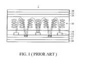
- FIG. 1is a cross section of a conventional fringe field switching liquid crystal display (FFS-LCD) device.
- An FFS-LCD 1comprises a lower substrate 10 , an upper substrate 20 , and a liquid crystal layer 30 interposed between the lower substrate 10 and the upper substrate 20 , serving as an LCD cell.
- a counter electrode 11 and a plurality of pixel electrodes 13are disposed on the lower substrate 10 .
- An insulating layer 15is disposed between the counter electrode 11 and the plurality of pixel electrodes 13 .
- a lower alignment layer 14is disposed on the insulating layer 15 and covers the pixel electrodes 13 .
- a color filter layer 25 and an upper alignment layer 24are disposed on the inner surface of the upper substrate 20 and are adjusted to the liquid crystal layer 30 .
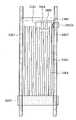
- FIG. 2is a plan view of the lower substrate structure of a conventional fringe field switching liquid crystal display (FFS-LCD) device.
- FFS-LCDfringe field switching liquid crystal display
- One parallel gate line 3 and two parallel data lines 7are orthogonally intersected, enclosing a pixel area.
- a counter electrode 11 and pixel electrodes 13are disposed in the pixel area.
- the pixel electrodes 13comprise two electrode bars 13 a parallel to the data lines 7 and a plurality of inclined electrodes 13 b with an inclined angle (p between the line m′ and the line m that is parallel to the gate line 3 .
- the two ends of each electrode 13 bare separately connected to the two electrode bras 13 a.
- the inclined angle ⁇ of the electrodes 13 bdirectly affects the operating voltage of the FFS-LCD device. More specifically, the greater the inclination of electrodes 13 b, the higher the voltage required to operate the FFS-LCD device.
- the inclined angle ⁇ of the electrodes 13 bmust be reduced to lower the operating voltage of the FFS-LCD device.
- a low inclined angle ⁇ of electrodes 13 be.g., less than 7°
- high inclined angle ⁇ of the electrodes 13 brequires a high driving voltage such that the physical area of the thin film transistor (TFT) must be increased to provide adequate charge storage capability.
- the TFT structurecomprises a gate line 3 , a channel and source/drain regions 4 , and source contact 6 a and drain contact 6 b.
- the drain contact 6 bconnects the pixel electrodes 13 via a contact plug 9 .
- FFS-LCD deviceswith improved aperture and transmittance ratios are desirable.
- FFS-LCD deviceswith improved aperture and transmittance ratios are proposed. Specifically, the FFS-LCD devices are fabricated by a reduced mask-count process.
- One embodiment of a system for displaying imagescomprises a display panel comprising: a lower substrate with a first surface, wherein the first surface is divided into a pixel area and a driver area; a peripheral circuit within the driver area on the first surface; at least one thin film transistor is formed in the pixel area, wherein the thin film transistor comprises an active layer, a gate dielectric layer overlies the active layer, and a gate electrode overlies the gate dielectric layer, and the active layer has source and drain regions; a first transparent electrode layer directly overlapped on a portion of the drain region, electrically connected thereto; and a second transparent electrode pattern disposed on the gate dielectric layer, opposing the first transparent electrode layer.
- Another embodiment of a fabrication method for a system for displaying imagescomprises: providing a display panel including a lower substrate with a first surface, wherein the first surface is divided into a pixel area and a driver area; forming first and second active layers overlying the driver area, and a third active layer overlying the pixel area; forming a first transparent electrode layer partially overlapping a portion of the third active layer; forming a gate dielectric layer overlying the first, second, third active layers, and a first transparent electrode layer; forming a second transparent electrode pattern overlying the gate dielectric layer, opposing the first transparent electrode layer; performing a first metallization (M 1 ), forming a first gate electrode overlying the first active layer, a second gate electrode overlying the second active layer, third and fourth gate electrodes overlying the third active layer, and a metal mask covering the second transparent electrode pattern; forming an interlayer dielectric layer overlying the overall lower substrate; performing a second metallization (M 2 ) on the overall lower substrate;
- FIG. 1is a cross section of a conventional fringe field switching liquid crystal display (FFS-LCD) device.
- FFS-LCDfringe field switching liquid crystal display
- FIG. 2is a plan view of the lower substrate structure of a conventional fringe field switching liquid crystal display (FFS-LCD) device.
- FFS-LCDfringe field switching liquid crystal display
- FIGS. 3A ⁇ 3Jshow an intermediate cross section of a system for displaying images in accordance with an embodiment of the invention.
- FIG. 3 kshows a top view of the resultant structure fabricated by the method of the embodiment.
- FIG. 4schematically shows another embodiment of a system for displaying images.
- FIGS. 3A ⁇ 3Jshow an intermediate cross section of a system for displaying images in accordance with an embodiment of the invention.
- a cleaned substrate 302used for fabricating a thin film transistor array substrate, comprising a driver area 304 where a peripheral circuit (not shown) is formed and a pixel area 306 is provided, and a buffer layer 308 is formed on the substrate 302 .
- the buffer layer 308can comprise silicon oxide, silicon nitride, silicon oxynitride or combinations thereof and preferably does a stack comprise a silicon oxide layer and a silicon nitride layer.
- thickness of the silicon nitride layeris about 350 ⁇ ⁇ 650 ⁇
- thickness of the silicon oxide layeris about 500 ⁇ ⁇ 1600 ⁇ .
- the semiconductor layercan comprise polysilicon.
- an amorphous silicon layeris first formed by deposition with chemical vapor deposition and then crystallized or annealed with excimer laser, ELA to form a polysilicon layer.
- the semiconductor layeris defined by conventional lithography and etched to form a first active layer 310 and a second active layer 312 which overly the driver area 304 of the substrate 302 and a third active layer 3101 overlying the pixel area 306 of the substrate 302 .
- thickness of the active layers 310 , 312 and 3101is between 350 ⁇ 500 ⁇ , for example, 430 ⁇ .
- the second active layer 312is covered by a photoresist layer 314 .
- a channel doping 316is performed on the active layers 310 and 3101 in which the dopant used can be boron (B+), and the dosage thereof is typically about 0 to 1E13/cm2.
- channel regions 3101 ′ and 3101 ′′ of the third active layer 3101are covered by a photoresist pattern 3141 (i.e. the so-called W-gate structure).
- a channel region 320 of the first active layer 310is covered by another photoresist layer 318 , implanting n-type dopant ions 322 into the first active layer 310 to form a source 324 and a drain 326 of an n type transistor.
- n-type dopant ionsare implanted into the exposed third active layer 3101 , thus, forming heavily doped n-type regions 3101 a, 3101 b and 3101 c thereof.
- the n-type dopant ionscan be phosphonium (PH x + ), and the dosage thereof is about 1E14 to 1E16/cm2.
- a first transparent electrode layer 3000is formed overlying the buffer layer 308 and is simultaneously attached to a portion of the n-type region 3101 b. Formation of the first transparent electrode layer 3000 includes sputtering, photolithography and etching, and the material thereof can be ITO or IZO. It is noted that the first transparent electrode layer 3000 is electrically connected to the n-type region 3101 b directly without the use of contact holes.
- a gate dielectric layer 3002for example silicon oxide, silicon nitride, silicon oxynitride, or combinations thereof, a stack layer thereof or another high dielectric constant material, is blanketly deposited on the first active layer 310 , the second active layer 312 , the third active layer 3101 , the first transparent electrode layer 3000 and the buffer layer 308 .
- Deposition of the gate dielectric layer 3002comprises CVD.
- a second transparent electrode pattern 3004also called ITO fingers
- Formation of the second transparent electrode layer 3010includes sputtering, photolithography and etching, and the material thereof can be ITO or IZO.
- a metal layer(not shown) is deposited and patterned to form scan lines (not shown), common electrodes (not shown), and gate electrodes (or gates) 330 , 332 , 3006 , 3008 , and a mask layer 3010 over the second transparent electrode.
- a lighter n-type dopingusing, for example, ion implantation, can be performed to form lightly doped drain (LDD) regions 324 a and 326 a on opposite sides of the channel region 320 of the first active layer 310 of the n type transistor.
- LDDlightly doped drain
- lightly doped drain (LDD) regions 3101 d and 3101 e on opposite sides of the channel region 3101 ′ and lightly doped drain (LDD) regions 3101 f and 3101 g on opposite sides of the channel region 3101 ′′are simultaneously formed.
- a mask 3010is formed overlying the second transparent electrode pattern 3004 prior to the LDD doping 3 ′, preventing second transparent electrode pattern 3004 from the striking of the ions.
- the second transparent electrode layer 3010is electrically connected to the common electrodes directly without the use of contact holes, and is a slit-like structure.
- the gate electrodes 3006 and 3008 , gate dielectric layer 3002 , and third active layer 3101construct a twin-gate structure i.e. two gates share the same active layer.
- a photoresist pattern 3011is formed to cover the whole substrate 302 , excluding the gate 332 and a portion of the gate dielectric layer 3002 .
- An ion implantation with p-type dopant 337is performed to form source 344 and drain 346 on opposite sides of the channel region 312 ′ of the p type transistor.
- the photoresist pattern 3011is removed.
- An interlayer dielectric layer 3012is blanketly deposited overlying the substrate.
- the thickness and composition of the dielectric layer 3011can be determined according to product specifications or process window.
- the interlayer dielectric layer 3012may include silicon dioxide, polyimide, spin-on-glass (SOG), fluoride-doped silicate glass (FSG), Black Diamond (a product of Applied Materials of Santa Clara, Calif.), Xerogel, Aerogel, amorphous fluorinated carbon, and/or other materials.
- the interlayer dielectric layer 3012is a stack layer comprising silicon oxide and silicon nitride. Formation of the interlayer dielectric layer 3012 comprises CVD. In addition, an annealing is conducted to activate the dopants.
- contact holes 3012 aare defined and etched through the interlayer dielectric layer 3012 and the gate dielectric layer 3002 .
- the etchingcomprises a dry etching or a wet etching to expose the second transparent electrode pattern 3004 and the mask 3010 .
- the mask 3010protects the dielectric layer 3002 between the slits of the transparent electrode pattern 3004 from being etched during the contact-hole etching.
- a conductive material filmis deposited, for example, by sputtering on the interlayer dielectric layer 3012 . As shown in FIG. 3J , the conductive material 3012 b fills the contact holes 3012 a.
- the conductive material 3012 bcan be metal or metal alloy.
- the data linesare also formed upon patterning and etching of the conductive layer. The mask 3010 is removed by etching during or after the etching of the data lines.
- a passivation layer and a planarization layermay be formed immediately or later. Since the subsequent steps are well known to those with ordinary skill in the art, they are omitted here for brevity.
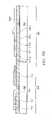
- FIG. 3 kshows a top view of the resultant structure fabricated by the previously described processes.
- the resultant structure of the embodimenthas less contact holes, thus enhancing the aperture ratio.
- FIG. 4schematically shows another embodiment of a system for displaying images which, in this example, is implemented as a fringe field switching mode liquid crystal display (FFS-LCD) device 30000 or an electronic device 50 .
- the previously described thin film transistor array substratecan be incorporated into a display panel that can be a fringe field switching mode liquid crystal display (FFS-LCD) panel.
- a fringe field switching mode liquid crystal display (FFS-LCD) devicecan be comprised of the display panel and a controller.
- the fringe field switching mode liquid crystal display (FFS-LCD) device 30000can form a portion of a variety of electronic devices (in this example, electronic device 50 ).
- the electronic device 50can comprise the fringe field switching mode liquid crystal display (FFS-LCD) device 30000 and the controller and an input unit 40 .
- the input unit 40is operatively coupled to the fringe field switching mode liquid crystal display (FFS-LCD) device 30000 and provides input signals (e.g., an image signal) to the display panel 20 to generate images.
- the electronic device 50can be a mobile phone, digital camera, PDA (personal digital assistant), notebook computer, desktop computer, television, car display, global positioning system (GPS), avionics display or portable DVD player, for example.
- the FFS structure of the described embodiments of the inventioncan be completed using only 9 masks, same as conventional non-FFS structures.
- the drain-side contact holese.g. the contact hole connected to the n-type region 3101 b
- the common electrodeis connected directly to the second transparent electrode, thus not requiring additional contact holes.
- two contact holesare reduced per pixel.
- the dielectric layer between the two transparent electrode layershas same thickness as the gate dielectric layer which is thinner than that used in conventional FFS structures, thus requiring less FFS driving voltage. Also, since this dielectric layer is thin, the storage capacitor value is high, hence the liquid crystal mode has less cross-talk, and can also withstand higher back-light intensity.
Landscapes
- Physics & Mathematics (AREA)
- Nonlinear Science (AREA)
- Geometry (AREA)
- Mathematical Physics (AREA)
- Chemical & Material Sciences (AREA)
- Crystallography & Structural Chemistry (AREA)
- General Physics & Mathematics (AREA)
- Optics & Photonics (AREA)
- Liquid Crystal (AREA)
- Thin Film Transistor (AREA)
- Devices For Indicating Variable Information By Combining Individual Elements (AREA)
Abstract
Description
- 1. Field of the Invention
- The present invention relates to liquid crystal display devices, and in particular relates to fringe field switching mode liquid crystal display (FFS-LCD) devices.
- 2. Description of the Related Art
- Liquid crystal display (LCD) devices possess the advantages of having a small size, being light weight and requiring low power consumption. Thus, LCD devices are being applied in a wide variety of electronic and communication devices including notebook computers, personal digital assistants (PDA), and mobile phones. Critical features for large-scale monitors and high-end TV applications, include a fast response time, a high contrast ratio, a high transparency, and a wide viewing angle without gray scale inversion. In-plane switching (IPS) mode liquid crystal display devices meet the above-mentioned high quality display feature requirements, and solve the viewing angle problems by orienting the liquid crystal molecules to be parallel with a substrate.
- Meanwhile, fringe field switching liquid crystal display (FFS-LCD) devices have pixel and counter electrodes comprising transparent conductors and a relatively narrower distance between electrodes than the distance between the upper and lower substrates to form a fringe field on the electrodes. During operation, the fringe field on the electrodes forces the substantially homogeneous liquid crystal molecules to rotate transversely between the substrates in which a wide viewing angle is accomplished since the light is transmitted through the horizontally arranged liquid crystal molecules. Moreover, since the counter electrode and the pixel electrode comprise transparent conductive materials, the aperture ratio and the transmittance ratio of the display devices can thereby be improved.
- U.S. Pat. No. 6,856,371, the entirety of which is hereby incorporated by reference, disclose electrode structures of a conventional FFS-LCD device. The electrode structures are symmetrical and render high image display quality and high transmittance ratio.
FIG. 1 is a cross section of a conventional fringe field switching liquid crystal display (FFS-LCD) device. An FFS-LCD 1 comprises alower substrate 10, an upper substrate20, and aliquid crystal layer 30 interposed between thelower substrate 10 and the upper substrate20, serving as an LCD cell. Acounter electrode 11 and a plurality ofpixel electrodes 13 are disposed on thelower substrate 10. Aninsulating layer 15 is disposed between thecounter electrode 11 and the plurality ofpixel electrodes 13. Alower alignment layer 14 is disposed on theinsulating layer 15 and covers thepixel electrodes 13. Acolor filter layer 25 and anupper alignment layer 24 are disposed on the inner surface of the upper substrate20 and are adjusted to theliquid crystal layer 30.FIG. 2 is a plan view of the lower substrate structure of a conventional fringe field switching liquid crystal display (FFS-LCD) device. Oneparallel gate line 3 and twoparallel data lines 7 are orthogonally intersected, enclosing a pixel area. Acounter electrode 11 andpixel electrodes 13 are disposed in the pixel area. Thepixel electrodes 13 comprise twoelectrode bars 13aparallel to thedata lines 7 and a plurality ofinclined electrodes 13bwith an inclined angle (p between the line m′ and the line m that is parallel to thegate line 3. The two ends of eachelectrode 13bare separately connected to the twoelectrode bras 13a.Note that the inclined angle φ of theelectrodes 13bdirectly affects the operating voltage of the FFS-LCD device. More specifically, the greater the inclination ofelectrodes 13b,the higher the voltage required to operate the FFS-LCD device.- For small FFS-LCD panels, the inclined angle φ of the
electrodes 13bmust be reduced to lower the operating voltage of the FFS-LCD device. A low inclined angle φ ofelectrodes 13b(e.g., less than 7°) can cause the disclination effect deteriorating display image quality. Conversely, high inclined angle φ of theelectrodes 13brequires a high driving voltage such that the physical area of the thin film transistor (TFT) must be increased to provide adequate charge storage capability. The TFT structure comprises agate line 3, a channel and source/drain regions 4, andsource contact 6aand draincontact 6b.Thedrain contact 6bconnects thepixel electrodes 13 via a contact plug9. When the physical area of the thin film transistor (TFT) increases, however, the area of thepixel electrodes 13 must be reduced, thus, a small aperture ratio and a low transmittance ratio occur. - Thus, FFS-LCD devices with improved aperture and transmittance ratios are desirable.
- In view of the previously described problems, various embodiments of FFS-LCD devices with improved aperture and transmittance ratios are proposed. Specifically, the FFS-LCD devices are fabricated by a reduced mask-count process.
- One embodiment of a system for displaying images, comprises a display panel comprising: a lower substrate with a first surface, wherein the first surface is divided into a pixel area and a driver area; a peripheral circuit within the driver area on the first surface; at least one thin film transistor is formed in the pixel area, wherein the thin film transistor comprises an active layer, a gate dielectric layer overlies the active layer, and a gate electrode overlies the gate dielectric layer, and the active layer has source and drain regions; a first transparent electrode layer directly overlapped on a portion of the drain region, electrically connected thereto; and a second transparent electrode pattern disposed on the gate dielectric layer, opposing the first transparent electrode layer.
- Another embodiment of a fabrication method for a system for displaying images, comprises: providing a display panel including a lower substrate with a first surface, wherein the first surface is divided into a pixel area and a driver area; forming first and second active layers overlying the driver area, and a third active layer overlying the pixel area; forming a first transparent electrode layer partially overlapping a portion of the third active layer; forming a gate dielectric layer overlying the first, second, third active layers, and a first transparent electrode layer; forming a second transparent electrode pattern overlying the gate dielectric layer, opposing the first transparent electrode layer; performing a first metallization (M1), forming a first gate electrode overlying the first active layer, a second gate electrode overlying the second active layer, third and fourth gate electrodes overlying the third active layer, and a metal mask covering the second transparent electrode pattern; forming an interlayer dielectric layer overlying the overall lower substrate; performing a second metallization (M2) on the overall lower substrate; forming a passivation layer overlying the overall lower substrate; and connecting the lower substrate to the upper substrate.
- A detailed description is given in the following embodiments with reference to the accompanying drawings.
- The present invention can be more fully understood by reading the subsequent detailed description and examples with references made to the accompanying drawings, wherein:
FIG. 1 is a cross section of a conventional fringe field switching liquid crystal display (FFS-LCD) device.FIG. 2 is a plan view of the lower substrate structure of a conventional fringe field switching liquid crystal display (FFS-LCD) device.FIGS. 3A˜3J show an intermediate cross section of a system for displaying images in accordance with an embodiment of the invention.FIG. 3 kshows a top view of the resultant structure fabricated by the method of the embodiment.FIG. 4 schematically shows another embodiment of a system for displaying images.- The following description is of the best-contemplated mode of carrying out the invention. This description is made for the purpose of illustrating the general principles of the invention and should not be taken in a limiting sense. The scope of the invention is best determined by reference to the appended claims.
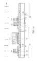
FIGS. 3A˜3J show an intermediate cross section of a system for displaying images in accordance with an embodiment of the invention. Referring toFIG. 3A , a cleanedsubstrate 302, used for fabricating a thin film transistor array substrate, comprising adriver area 304 where a peripheral circuit (not shown) is formed and apixel area 306 is provided, and abuffer layer 308 is formed on thesubstrate 302. Thebuffer layer 308 can comprise silicon oxide, silicon nitride, silicon oxynitride or combinations thereof and preferably does a stack comprise a silicon oxide layer and a silicon nitride layer. In one embodiment of the invention, thickness of the silicon nitride layer is about 350 Ř650 Å, and thickness of the silicon oxide layer is about 500 Ř1600 Å.- Next, a semiconductor layer (not shown) is formed on the
buffer layer 308. The semiconductor layer can comprise polysilicon. For example, an amorphous silicon layer is first formed by deposition with chemical vapor deposition and then crystallized or annealed with excimer laser, ELA to form a polysilicon layer. The semiconductor layer is defined by conventional lithography and etched to form a firstactive layer 310 and a secondactive layer 312 which overly thedriver area 304 of thesubstrate 302 and a thirdactive layer 3101 overlying thepixel area 306 of thesubstrate 302. In one embodiment of the invention, thickness of theactive layers - Referring to
FIG. 3B , the secondactive layer 312 is covered by aphotoresist layer 314. Achannel doping 316 is performed on theactive layers - Referring to
FIG. 3C ,channel regions 3101′ and3101″ of the thirdactive layer 3101 are covered by a photoresist pattern3141 (i.e. the so-called W-gate structure). Achannel region 320 of the firstactive layer 310 is covered by anotherphotoresist layer 318, implanting n-type dopant ions 322 into the firstactive layer 310 to form asource 324 and adrain 326 of an n type transistor. Meanwhile, n-type dopant ions are implanted into the exposed thirdactive layer 3101, thus, forming heavily doped n-type regions - Referring to
FIG. 3D , after the photoresist layers314,3141 and318 are removed, a firsttransparent electrode layer 3000 is formed overlying thebuffer layer 308 and is simultaneously attached to a portion of the n-type region 3101b.Formation of the firsttransparent electrode layer 3000 includes sputtering, photolithography and etching, and the material thereof can be ITO or IZO. It is noted that the firsttransparent electrode layer 3000 is electrically connected to the n-type region 3101bdirectly without the use of contact holes. - Referring to
FIG. 3E , agate dielectric layer 3002, for example silicon oxide, silicon nitride, silicon oxynitride, or combinations thereof, a stack layer thereof or another high dielectric constant material, is blanketly deposited on the firstactive layer 310, the secondactive layer 312, the thirdactive layer 3101, the firsttransparent electrode layer 3000 and thebuffer layer 308. Deposition of thegate dielectric layer 3002 comprises CVD. Thereafter, a second transparent electrode pattern3004 (also called ITO fingers) is formed on thegate dielectric layer 3002. Formation of the secondtransparent electrode layer 3010 includes sputtering, photolithography and etching, and the material thereof can be ITO or IZO. - As shown in
FIG. 3F , a metal layer (not shown) is deposited and patterned to form scan lines (not shown), common electrodes (not shown), and gate electrodes (or gates)330,332,3006,3008, and amask layer 3010 over the second transparent electrode. Next, a lighter n-type doping using, for example, ion implantation, can be performed to form lightly doped drain (LDD)regions channel region 320 of the firstactive layer 310 of the n type transistor. In addition, lightly doped drain (LDD)regions channel region 3101′ and lightly doped drain (LDD)regions channel region 3101″ are simultaneously formed. It is noted that amask 3010 is formed overlying the secondtransparent electrode pattern 3004 prior to theLDD doping 3′, preventing secondtransparent electrode pattern 3004 from the striking of the ions. In addition, the secondtransparent electrode layer 3010 is electrically connected to the common electrodes directly without the use of contact holes, and is a slit-like structure. Thegate electrodes gate dielectric layer 3002, and thirdactive layer 3101 construct a twin-gate structure i.e. two gates share the same active layer. - In
FIG. 3G , aphotoresist pattern 3011 is formed to cover thewhole substrate 302, excluding thegate 332 and a portion of thegate dielectric layer 3002. An ion implantation with p-type dopant 337 is performed to formsource 344 and drain346 on opposite sides of thechannel region 312′ of the p type transistor. - Next, referring to
FIG. 3H , thephotoresist pattern 3011 is removed. Aninterlayer dielectric layer 3012 is blanketly deposited overlying the substrate. Generally, the thickness and composition of thedielectric layer 3011 can be determined according to product specifications or process window. For example, theinterlayer dielectric layer 3012 may include silicon dioxide, polyimide, spin-on-glass (SOG), fluoride-doped silicate glass (FSG), Black Diamond (a product of Applied Materials of Santa Clara, Calif.), Xerogel, Aerogel, amorphous fluorinated carbon, and/or other materials. In this embodiment of the invention, theinterlayer dielectric layer 3012 is a stack layer comprising silicon oxide and silicon nitride. Formation of theinterlayer dielectric layer 3012 comprises CVD. In addition, an annealing is conducted to activate the dopants. - As shown in
FIG. 3I , by means of sequential patterning and etching processes,contact holes 3012aare defined and etched through theinterlayer dielectric layer 3012 and thegate dielectric layer 3002. The etching comprises a dry etching or a wet etching to expose the secondtransparent electrode pattern 3004 and themask 3010. Themask 3010 protects thedielectric layer 3002 between the slits of thetransparent electrode pattern 3004 from being etched during the contact-hole etching. - A conductive material film is deposited, for example, by sputtering on the
interlayer dielectric layer 3012. As shown inFIG. 3J , theconductive material 3012bfills the contact holes3012a.Theconductive material 3012bcan be metal or metal alloy. The data lines are also formed upon patterning and etching of the conductive layer. Themask 3010 is removed by etching during or after the etching of the data lines. - Thereafter, formation of a passivation layer and a planarization layer may be performed immediately or later. Since the subsequent steps are well known to those with ordinary skill in the art, they are omitted here for brevity.
FIG. 3 kshows a top view of the resultant structure fabricated by the previously described processes. Compared to the conventional structure inFIGS. 1 and 2 , the resultant structure of the embodiment has less contact holes, thus enhancing the aperture ratio.FIG. 4 schematically shows another embodiment of a system for displaying images which, in this example, is implemented as a fringe field switching mode liquid crystal display (FFS-LCD)device 30000 or anelectronic device 50. The previously described thin film transistor array substrate can be incorporated into a display panel that can be a fringe field switching mode liquid crystal display (FFS-LCD) panel. In other embodiments, a fringe field switching mode liquid crystal display (FFS-LCD) device can be comprised of the display panel and a controller. In other embodiments, the fringe field switching mode liquid crystal display (FFS-LCD)device 30000 can form a portion of a variety of electronic devices (in this example, electronic device50). Generally, theelectronic device 50 can comprise the fringe field switching mode liquid crystal display (FFS-LCD)device 30000 and the controller and aninput unit 40. Further, theinput unit 40 is operatively coupled to the fringe field switching mode liquid crystal display (FFS-LCD)device 30000 and provides input signals (e.g., an image signal) to the display panel20 to generate images. Theelectronic device 50 can be a mobile phone, digital camera, PDA (personal digital assistant), notebook computer, desktop computer, television, car display, global positioning system (GPS), avionics display or portable DVD player, for example.- The FFS structure of the described embodiments of the invention can be completed using only 9 masks, same as conventional non-FFS structures. The drain-side contact holes (e.g. the contact hole connected to the n-
type region 3101b) are not needed, thus improving the aperture ratio. Additionally, as was mentioned before, the common electrode is connected directly to the second transparent electrode, thus not requiring additional contact holes. Accordingly, compared to the prior art of forming FFS TFT structures, two contact holes are reduced per pixel. The dielectric layer between the two transparent electrode layers has same thickness as the gate dielectric layer which is thinner than that used in conventional FFS structures, thus requiring less FFS driving voltage. Also, since this dielectric layer is thin, the storage capacitor value is high, hence the liquid crystal mode has less cross-talk, and can also withstand higher back-light intensity. - While the invention has been described by way of example and in terms of the preferred embodiments, it is to be understood that the invention is not limited to the disclosed embodiments. To the contrary, it is intended to cover various modifications and similar arrangements (as would be apparent to those skilled in the art). Therefore, the scope of the appended claims should be accorded the broadest interpretation so as to encompass all such modifications and similar arrangements.
Claims (14)
Priority Applications (3)
| Application Number | Priority Date | Filing Date | Title |
|---|---|---|---|
| US12/051,006US8294840B2 (en) | 2008-03-19 | 2008-03-19 | Liquid crystal display device with fringe field switching mode |
| TW098107518ATWI386741B (en) | 2008-03-19 | 2009-03-09 | System for displaying images and fabrication method thereof |
| CN2009101198324ACN101539691B (en) | 2008-03-19 | 2009-03-19 | Image display system and manufacturing method thereof |
Applications Claiming Priority (1)
| Application Number | Priority Date | Filing Date | Title |
|---|---|---|---|
| US12/051,006US8294840B2 (en) | 2008-03-19 | 2008-03-19 | Liquid crystal display device with fringe field switching mode |
Publications (2)
| Publication Number | Publication Date |
|---|---|
| US20090237582A1true US20090237582A1 (en) | 2009-09-24 |
| US8294840B2 US8294840B2 (en) | 2012-10-23 |
Family
ID=41088513
Family Applications (1)
| Application Number | Title | Priority Date | Filing Date |
|---|---|---|---|
| US12/051,006Active2030-01-12US8294840B2 (en) | 2008-03-19 | 2008-03-19 | Liquid crystal display device with fringe field switching mode |
Country Status (3)
| Country | Link |
|---|---|
| US (1) | US8294840B2 (en) |
| CN (1) | CN101539691B (en) |
| TW (1) | TWI386741B (en) |
Cited By (3)
| Publication number | Priority date | Publication date | Assignee | Title |
|---|---|---|---|---|
| US20140014944A1 (en)* | 2012-07-16 | 2014-01-16 | E Ink Holdings Inc. | Pixel structure and fabrication method thereof |
| US20140319555A1 (en)* | 2013-04-30 | 2014-10-30 | Samsung Display Co., Ltd. | Display panel and display apparatus having the same |
| CN106992201A (en)* | 2016-01-20 | 2017-07-28 | 三星显示有限公司 | Organic light-emitting display device |
Families Citing this family (7)
| Publication number | Priority date | Publication date | Assignee | Title |
|---|---|---|---|---|
| TWI402592B (en)* | 2010-04-06 | 2013-07-21 | Wintek Corp | Pixel structure |
| CN103035652B (en)* | 2011-09-30 | 2015-08-05 | 深超光电(深圳)有限公司 | Array substrate of fringe field switching type liquid crystal display panel and method of fabricating the same |
| CN103777395A (en) | 2014-01-27 | 2014-05-07 | 京东方科技集团股份有限公司 | Array substrate as well as production method thereof and display device |
| CN106887386A (en)* | 2016-12-27 | 2017-06-23 | 北京理工大学 | The method that quasi-molecule laser annealing prepares bridge-type raceway groove polysilicon membrane |
| TWI605284B (en)* | 2016-12-30 | 2017-11-11 | 友達光電股份有限公司 | Pixel structure |
| CN108257975B (en)* | 2018-01-02 | 2022-10-04 | 京东方科技集团股份有限公司 | Array substrate and preparation method thereof, display device and preparation method of thin film transistor |
| CN114822242B (en)* | 2022-03-11 | 2023-03-10 | 惠科股份有限公司 | Backlight module and display device |
Citations (5)
| Publication number | Priority date | Publication date | Assignee | Title |
|---|---|---|---|---|
| US5182620A (en)* | 1990-04-05 | 1993-01-26 | Sharp Kabushiki Kaisha | Active matrix display device |
| US6650385B1 (en)* | 2002-04-24 | 2003-11-18 | Prime View International Co., Ltd. | Scattering fringe field optical-compensated reflective and transflective liquid crystal display |
| US6784955B2 (en)* | 2001-10-01 | 2004-08-31 | The Hong Kong University Of Science And Technology | Optically optimized permanently bistable twisted nematic liquid crystal displays |
| US6856371B2 (en)* | 2001-05-07 | 2005-02-15 | Boe-Hydis Technology Co., Ltd. | In plane fringe field switching mode LCD realizing high screen quality |
| US20050214983A1 (en)* | 2004-03-26 | 2005-09-29 | Semiconductor Energy Laboratory Co., Ltd. | Semiconductor device, method for manufacturing the same, liquid crystal television and EL television |
Family Cites Families (5)
| Publication number | Priority date | Publication date | Assignee | Title |
|---|---|---|---|---|
| JPH0290963A (en)* | 1988-09-26 | 1990-03-30 | Mazda Motor Corp | Device for changing color in coating |
| US5042918A (en)* | 1988-11-15 | 1991-08-27 | Kabushiki Kaisha Toshiba | Liquid crystal display device |
| US5929464A (en)* | 1995-01-20 | 1999-07-27 | Semiconductor Energy Laboratory Co., Ltd. | Active matrix electro-optical device |
| JP3617800B2 (en)* | 1999-12-28 | 2005-02-09 | 松下電器産業株式会社 | TFT array substrate and its manufacturing method Liquid crystal display device using the same |
| TW594622B (en)* | 2002-10-17 | 2004-06-21 | Toppoly Optoelectronics Corp | Wide viewing angle LCD and manufacturing method thereof |
- 2008
- 2008-03-19USUS12/051,006patent/US8294840B2/enactiveActive
- 2009
- 2009-03-09TWTW098107518Apatent/TWI386741B/ennot_activeIP Right Cessation
- 2009-03-19CNCN2009101198324Apatent/CN101539691B/enactiveActive
Patent Citations (5)
| Publication number | Priority date | Publication date | Assignee | Title |
|---|---|---|---|---|
| US5182620A (en)* | 1990-04-05 | 1993-01-26 | Sharp Kabushiki Kaisha | Active matrix display device |
| US6856371B2 (en)* | 2001-05-07 | 2005-02-15 | Boe-Hydis Technology Co., Ltd. | In plane fringe field switching mode LCD realizing high screen quality |
| US6784955B2 (en)* | 2001-10-01 | 2004-08-31 | The Hong Kong University Of Science And Technology | Optically optimized permanently bistable twisted nematic liquid crystal displays |
| US6650385B1 (en)* | 2002-04-24 | 2003-11-18 | Prime View International Co., Ltd. | Scattering fringe field optical-compensated reflective and transflective liquid crystal display |
| US20050214983A1 (en)* | 2004-03-26 | 2005-09-29 | Semiconductor Energy Laboratory Co., Ltd. | Semiconductor device, method for manufacturing the same, liquid crystal television and EL television |
Cited By (5)
| Publication number | Priority date | Publication date | Assignee | Title |
|---|---|---|---|---|
| US20140014944A1 (en)* | 2012-07-16 | 2014-01-16 | E Ink Holdings Inc. | Pixel structure and fabrication method thereof |
| US9684216B2 (en)* | 2012-07-16 | 2017-06-20 | E Ink Holdings Inc. | Pixel structure and fabrication method thereof |
| US20140319555A1 (en)* | 2013-04-30 | 2014-10-30 | Samsung Display Co., Ltd. | Display panel and display apparatus having the same |
| US9431502B2 (en)* | 2013-04-30 | 2016-08-30 | Samsung Display Co., Ltd. | Display panel and display apparatus having the same |
| CN106992201A (en)* | 2016-01-20 | 2017-07-28 | 三星显示有限公司 | Organic light-emitting display device |
Also Published As
| Publication number | Publication date |
|---|---|
| US8294840B2 (en) | 2012-10-23 |
| CN101539691A (en) | 2009-09-23 |
| TW200941106A (en) | 2009-10-01 |
| CN101539691B (en) | 2013-08-07 |
| TWI386741B (en) | 2013-02-21 |
Similar Documents
| Publication | Publication Date | Title |
|---|---|---|
| US8294840B2 (en) | Liquid crystal display device with fringe field switching mode | |
| KR100675631B1 (en) | Transverse electric field liquid crystal display device and manufacturing method thereof | |
| US20090251628A1 (en) | Pixel structure of liquid crystal display panel and method of making the same | |
| JP3964223B2 (en) | Thin film transistor device | |
| US8420413B2 (en) | Method for manufacturing pixel structure | |
| US6852577B2 (en) | Method for forming a low temperature polysilicon CMOS thin film transistor | |
| US7973317B2 (en) | Array substrate for liquid crystal display and method for fabricating the same | |
| KR20010083207A (en) | A semiconductor device and method of manufacturing the same | |
| US20080197356A1 (en) | Thin film transistor substrate and method of manufacturing the same | |
| CN116224666B (en) | Array substrate, preparation method thereof, display panel and display device | |
| US9281325B2 (en) | Array substrate, manufacturing method thereof and display device | |
| US7924355B2 (en) | Liquid crystal display device | |
| CN101853883B (en) | Thin film transistor, manufacturing method thereof, liquid crystal display panel and electronic device using same | |
| US7371624B2 (en) | Method of manufacturing thin film semiconductor device, thin film semiconductor device, electro-optical device, and electronic apparatus | |
| US20070051954A1 (en) | TFT array substrate of TFT LCD having large storage capcitor and method for manufacturing same | |
| JPH10111520A (en) | Liquid crystal display panel and electronic device using the same | |
| JP2002033331A (en) | Semiconductor device and manufacturing method thereof | |
| JP3791225B2 (en) | Electro-optical panel and electronic equipment | |
| JP2001281645A (en) | Electro-optical device | |
| US7053408B2 (en) | Liquid crystal display device having enlarged channel region and fabricating method thereof | |
| JP2009021320A (en) | Semiconductor device manufacturing method, semiconductor device, and electronic apparatus | |
| JP3647384B2 (en) | Thin film semiconductor device, manufacturing method thereof, and display panel | |
| KR101294693B1 (en) | The array substrate for liquid crystal display device | |
| CN101097370B (en) | Liquid crystal display and manufacturing method thereof | |
| JP2009210681A (en) | Display and manufacturing method therefor |
Legal Events
| Date | Code | Title | Description |
|---|---|---|---|
| AS | Assignment | Owner name:TPO DISPLAYS CORP., TAIWAN Free format text:ASSIGNMENT OF ASSIGNORS INTEREST;ASSIGNORS:KAKKAD, RAMESH;LIN, CHIEH-WEN;REEL/FRAME:020672/0036;SIGNING DATES FROM 20080303 TO 20080304 Owner name:TPO DISPLAYS CORP., TAIWAN Free format text:ASSIGNMENT OF ASSIGNORS INTEREST;ASSIGNORS:KAKKAD, RAMESH;LIN, CHIEH-WEN;SIGNING DATES FROM 20080303 TO 20080304;REEL/FRAME:020672/0036 | |
| AS | Assignment | Owner name:CHIMEI INNOLUX CORPORATION, TAIWAN Free format text:MERGER;ASSIGNOR:TPO DISPLAYS CORP.;REEL/FRAME:025738/0088 Effective date:20100318 | |
| STCF | Information on status: patent grant | Free format text:PATENTED CASE | |
| AS | Assignment | Owner name:INNOLUX CORPORATION, TAIWAN Free format text:CHANGE OF NAME;ASSIGNOR:CHIMEI INNOLUX CORPORATION;REEL/FRAME:032621/0718 Effective date:20121219 | |
| FEPP | Fee payment procedure | Free format text:PAYOR NUMBER ASSIGNED (ORIGINAL EVENT CODE: ASPN); ENTITY STATUS OF PATENT OWNER: LARGE ENTITY Free format text:PAYER NUMBER DE-ASSIGNED (ORIGINAL EVENT CODE: RMPN); ENTITY STATUS OF PATENT OWNER: LARGE ENTITY | |
| FPAY | Fee payment | Year of fee payment:4 | |
| MAFP | Maintenance fee payment | Free format text:PAYMENT OF MAINTENANCE FEE, 8TH YEAR, LARGE ENTITY (ORIGINAL EVENT CODE: M1552); ENTITY STATUS OF PATENT OWNER: LARGE ENTITY Year of fee payment:8 | |
| MAFP | Maintenance fee payment | Free format text:PAYMENT OF MAINTENANCE FEE, 12TH YEAR, LARGE ENTITY (ORIGINAL EVENT CODE: M1553); ENTITY STATUS OF PATENT OWNER: LARGE ENTITY Year of fee payment:12 | |
| AS | Assignment | Owner name:RED OAK INNOVATIONS LIMITED, IRELAND Free format text:ASSIGNMENT OF ASSIGNORS INTEREST;ASSIGNOR:INNOLUX CORPORATION;REEL/FRAME:069206/0903 Effective date:20240925 |