US20090236669A1 - Metal gate transistor and polysilicon resistor and method for fabricating the same - Google Patents
Metal gate transistor and polysilicon resistor and method for fabricating the sameDownload PDFInfo
- Publication number
- US20090236669A1 US20090236669A1US12/052,728US5272808AUS2009236669A1US 20090236669 A1US20090236669 A1US 20090236669A1US 5272808 AUS5272808 AUS 5272808AUS 2009236669 A1US2009236669 A1US 2009236669A1
- Authority
- US
- United States
- Prior art keywords
- polysilicon
- resistor
- transistor
- region
- metal gate
- Prior art date
- Legal status (The legal status is an assumption and is not a legal conclusion. Google has not performed a legal analysis and makes no representation as to the accuracy of the status listed.)
- Granted
Links
- 229910021420polycrystalline siliconInorganic materials0.000titleclaimsabstractdescription144
- 229920005591polysiliconPolymers0.000titleclaimsabstractdescription144
- 229910052751metalInorganic materials0.000titleclaimsabstractdescription90
- 239000002184metalSubstances0.000titleclaimsabstractdescription90
- 238000000034methodMethods0.000titleclaimsabstractdescription52
- 239000000758substrateSubstances0.000claimsabstractdescription32
- 239000010410layerSubstances0.000claimsdescription92
- 239000004065semiconductorSubstances0.000claimsdescription22
- 125000006850spacer groupChemical group0.000claimsdescription21
- 238000007517polishing processMethods0.000claimsdescription16
- 238000005530etchingMethods0.000claimsdescription14
- 239000011229interlayerSubstances0.000claimsdescription11
- 239000000126substanceSubstances0.000claimsdescription11
- 229910052581Si3N4Inorganic materials0.000claimsdescription6
- HQVNEWCFYHHQES-UHFFFAOYSA-Nsilicon nitrideChemical compoundN12[Si]34N5[Si]62N3[Si]51N64HQVNEWCFYHHQES-UHFFFAOYSA-N0.000claimsdescription6
- 229910000577Silicon-germaniumInorganic materials0.000claimsdescription4
- LEVVHYCKPQWKOP-UHFFFAOYSA-N[Si].[Ge]Chemical compound[Si].[Ge]LEVVHYCKPQWKOP-UHFFFAOYSA-N0.000claimsdescription4
- 229910021332silicideInorganic materials0.000claimsdescription4
- 238000000059patterningMethods0.000claimsdescription3
- FVBUAEGBCNSCDD-UHFFFAOYSA-Nsilicide(4-)Chemical compound[Si-4]FVBUAEGBCNSCDD-UHFFFAOYSA-N0.000claimsdescription3
- 238000000151depositionMethods0.000claimsdescription2
- 229920002120photoresistant polymerPolymers0.000description23
- 239000002019doping agentSubstances0.000description5
- 238000005468ion implantationMethods0.000description5
- 239000000463materialSubstances0.000description5
- VYPSYNLAJGMNEJ-UHFFFAOYSA-NSilicium dioxideChemical compoundO=[Si]=OVYPSYNLAJGMNEJ-UHFFFAOYSA-N0.000description4
- 230000015572biosynthetic processEffects0.000description4
- 239000007943implantSubstances0.000description4
- 238000004519manufacturing processMethods0.000description4
- 229910052814silicon oxideInorganic materials0.000description4
- 239000003990capacitorSubstances0.000description3
- 238000005498polishingMethods0.000description3
- KDLHZDBZIXYQEI-UHFFFAOYSA-NPalladiumChemical compound[Pd]KDLHZDBZIXYQEI-UHFFFAOYSA-N0.000description2
- XUIMIQQOPSSXEZ-UHFFFAOYSA-NSiliconChemical compound[Si]XUIMIQQOPSSXEZ-UHFFFAOYSA-N0.000description2
- 238000001312dry etchingMethods0.000description2
- BASFCYQUMIYNBI-UHFFFAOYSA-NplatinumChemical compound[Pt]BASFCYQUMIYNBI-UHFFFAOYSA-N0.000description2
- 229910052710siliconInorganic materials0.000description2
- 239000010703siliconSubstances0.000description2
- ZOKXTWBITQBERF-UHFFFAOYSA-NMolybdenumChemical compound[Mo]ZOKXTWBITQBERF-UHFFFAOYSA-N0.000description1
- RTAQQCXQSZGOHL-UHFFFAOYSA-NTitaniumChemical compound[Ti]RTAQQCXQSZGOHL-UHFFFAOYSA-N0.000description1
- 230000004075alterationEffects0.000description1
- 229910017052cobaltInorganic materials0.000description1
- 239000010941cobaltSubstances0.000description1
- GUTLYIVDDKVIGB-UHFFFAOYSA-Ncobalt atomChemical compound[Co]GUTLYIVDDKVIGB-UHFFFAOYSA-N0.000description1
- 239000003989dielectric materialSubstances0.000description1
- 230000000694effectsEffects0.000description1
- 239000012212insulatorSubstances0.000description1
- 230000010354integrationEffects0.000description1
- 150000002500ionsChemical class0.000description1
- 238000002955isolationMethods0.000description1
- 229910044991metal oxideInorganic materials0.000description1
- 150000004706metal oxidesChemical class0.000description1
- 238000012986modificationMethods0.000description1
- 230000004048modificationEffects0.000description1
- 229910052750molybdenumInorganic materials0.000description1
- 239000011733molybdenumSubstances0.000description1
- 229910052763palladiumInorganic materials0.000description1
- 229910052697platinumInorganic materials0.000description1
- 238000004151rapid thermal annealingMethods0.000description1
- 229910052719titaniumInorganic materials0.000description1
- 239000010936titaniumSubstances0.000description1
- 238000001039wet etchingMethods0.000description1
Images


Classifications
- H—ELECTRICITY
- H01—ELECTRIC ELEMENTS
- H01L—SEMICONDUCTOR DEVICES NOT COVERED BY CLASS H10
- H01L21/00—Processes or apparatus adapted for the manufacture or treatment of semiconductor or solid state devices or of parts thereof
- H01L21/02—Manufacture or treatment of semiconductor devices or of parts thereof
- H01L21/04—Manufacture or treatment of semiconductor devices or of parts thereof the devices having potential barriers, e.g. a PN junction, depletion layer or carrier concentration layer
- H01L21/18—Manufacture or treatment of semiconductor devices or of parts thereof the devices having potential barriers, e.g. a PN junction, depletion layer or carrier concentration layer the devices having semiconductor bodies comprising elements of Group IV of the Periodic Table or AIIIBV compounds with or without impurities, e.g. doping materials
- H01L21/28—Manufacture of electrodes on semiconductor bodies using processes or apparatus not provided for in groups H01L21/20 - H01L21/268
- H01L21/28008—Making conductor-insulator-semiconductor electrodes
- H01L21/28017—Making conductor-insulator-semiconductor electrodes the insulator being formed after the semiconductor body, the semiconductor being silicon
- H01L21/28026—Making conductor-insulator-semiconductor electrodes the insulator being formed after the semiconductor body, the semiconductor being silicon characterised by the conductor
- H01L21/28079—Making conductor-insulator-semiconductor electrodes the insulator being formed after the semiconductor body, the semiconductor being silicon characterised by the conductor the final conductor layer next to the insulator being a single metal, e.g. Ta, W, Mo, Al
- H—ELECTRICITY
- H10—SEMICONDUCTOR DEVICES; ELECTRIC SOLID-STATE DEVICES NOT OTHERWISE PROVIDED FOR
- H10D—INORGANIC ELECTRIC SEMICONDUCTOR DEVICES
- H10D64/00—Electrodes of devices having potential barriers
- H10D64/01—Manufacture or treatment
- H10D64/017—Manufacture or treatment using dummy gates in processes wherein at least parts of the final gates are self-aligned to the dummy gates, i.e. replacement gate processes
- H—ELECTRICITY
- H10—SEMICONDUCTOR DEVICES; ELECTRIC SOLID-STATE DEVICES NOT OTHERWISE PROVIDED FOR
- H10D—INORGANIC ELECTRIC SEMICONDUCTOR DEVICES
- H10D64/00—Electrodes of devices having potential barriers
- H10D64/60—Electrodes characterised by their materials
- H10D64/66—Electrodes having a conductor capacitively coupled to a semiconductor by an insulator, e.g. MIS electrodes
- H10D64/665—Electrodes having a conductor capacitively coupled to a semiconductor by an insulator, e.g. MIS electrodes the conductor comprising a layer of elemental metal contacting the insulator, e.g. tungsten or molybdenum
- H10D64/666—Electrodes having a conductor capacitively coupled to a semiconductor by an insulator, e.g. MIS electrodes the conductor comprising a layer of elemental metal contacting the insulator, e.g. tungsten or molybdenum the conductor further comprising additional layers
- H—ELECTRICITY
- H10—SEMICONDUCTOR DEVICES; ELECTRIC SOLID-STATE DEVICES NOT OTHERWISE PROVIDED FOR
- H10D—INORGANIC ELECTRIC SEMICONDUCTOR DEVICES
- H10D84/00—Integrated devices formed in or on semiconductor substrates that comprise only semiconducting layers, e.g. on Si wafers or on GaAs-on-Si wafers
- H10D84/01—Manufacture or treatment
- H10D84/0123—Integrating together multiple components covered by H10D12/00 or H10D30/00, e.g. integrating multiple IGBTs
- H10D84/0126—Integrating together multiple components covered by H10D12/00 or H10D30/00, e.g. integrating multiple IGBTs the components including insulated gates, e.g. IGFETs
- H10D84/0165—Integrating together multiple components covered by H10D12/00 or H10D30/00, e.g. integrating multiple IGBTs the components including insulated gates, e.g. IGFETs the components including complementary IGFETs, e.g. CMOS devices
- H10D84/0167—Manufacturing their channels
- H—ELECTRICITY
- H10—SEMICONDUCTOR DEVICES; ELECTRIC SOLID-STATE DEVICES NOT OTHERWISE PROVIDED FOR
- H10D—INORGANIC ELECTRIC SEMICONDUCTOR DEVICES
- H10D84/00—Integrated devices formed in or on semiconductor substrates that comprise only semiconducting layers, e.g. on Si wafers or on GaAs-on-Si wafers
- H10D84/01—Manufacture or treatment
- H10D84/0123—Integrating together multiple components covered by H10D12/00 or H10D30/00, e.g. integrating multiple IGBTs
- H10D84/0126—Integrating together multiple components covered by H10D12/00 or H10D30/00, e.g. integrating multiple IGBTs the components including insulated gates, e.g. IGFETs
- H10D84/0165—Integrating together multiple components covered by H10D12/00 or H10D30/00, e.g. integrating multiple IGBTs the components including insulated gates, e.g. IGFETs the components including complementary IGFETs, e.g. CMOS devices
- H10D84/017—Manufacturing their source or drain regions, e.g. silicided source or drain regions
- H—ELECTRICITY
- H10—SEMICONDUCTOR DEVICES; ELECTRIC SOLID-STATE DEVICES NOT OTHERWISE PROVIDED FOR
- H10D—INORGANIC ELECTRIC SEMICONDUCTOR DEVICES
- H10D84/00—Integrated devices formed in or on semiconductor substrates that comprise only semiconducting layers, e.g. on Si wafers or on GaAs-on-Si wafers
- H10D84/01—Manufacture or treatment
- H10D84/0123—Integrating together multiple components covered by H10D12/00 or H10D30/00, e.g. integrating multiple IGBTs
- H10D84/0126—Integrating together multiple components covered by H10D12/00 or H10D30/00, e.g. integrating multiple IGBTs the components including insulated gates, e.g. IGFETs
- H10D84/0165—Integrating together multiple components covered by H10D12/00 or H10D30/00, e.g. integrating multiple IGBTs the components including insulated gates, e.g. IGFETs the components including complementary IGFETs, e.g. CMOS devices
- H10D84/0172—Manufacturing their gate conductors
- H10D84/0177—Manufacturing their gate conductors the gate conductors having different materials or different implants
- H—ELECTRICITY
- H10—SEMICONDUCTOR DEVICES; ELECTRIC SOLID-STATE DEVICES NOT OTHERWISE PROVIDED FOR
- H10D—INORGANIC ELECTRIC SEMICONDUCTOR DEVICES
- H10D84/00—Integrated devices formed in or on semiconductor substrates that comprise only semiconducting layers, e.g. on Si wafers or on GaAs-on-Si wafers
- H10D84/01—Manufacture or treatment
- H10D84/02—Manufacture or treatment characterised by using material-based technologies
- H10D84/03—Manufacture or treatment characterised by using material-based technologies using Group IV technology, e.g. silicon technology or silicon-carbide [SiC] technology
- H10D84/038—Manufacture or treatment characterised by using material-based technologies using Group IV technology, e.g. silicon technology or silicon-carbide [SiC] technology using silicon technology, e.g. SiGe
- H—ELECTRICITY
- H10—SEMICONDUCTOR DEVICES; ELECTRIC SOLID-STATE DEVICES NOT OTHERWISE PROVIDED FOR
- H10D—INORGANIC ELECTRIC SEMICONDUCTOR DEVICES
- H10D84/00—Integrated devices formed in or on semiconductor substrates that comprise only semiconducting layers, e.g. on Si wafers or on GaAs-on-Si wafers
- H10D84/80—Integrated devices formed in or on semiconductor substrates that comprise only semiconducting layers, e.g. on Si wafers or on GaAs-on-Si wafers characterised by the integration of at least one component covered by groups H10D12/00 or H10D30/00, e.g. integration of IGFETs
- H10D84/811—Combinations of field-effect devices and one or more diodes, capacitors or resistors
- H—ELECTRICITY
- H10—SEMICONDUCTOR DEVICES; ELECTRIC SOLID-STATE DEVICES NOT OTHERWISE PROVIDED FOR
- H10D—INORGANIC ELECTRIC SEMICONDUCTOR DEVICES
- H10D30/00—Field-effect transistors [FET]
- H10D30/01—Manufacture or treatment
- H10D30/021—Manufacture or treatment of FETs having insulated gates [IGFET]
- H10D30/0223—Manufacture or treatment of FETs having insulated gates [IGFET] having source and drain regions or source and drain extensions self-aligned to sides of the gate
- H10D30/0227—Manufacture or treatment of FETs having insulated gates [IGFET] having source and drain regions or source and drain extensions self-aligned to sides of the gate having both lightly-doped source and drain extensions and source and drain regions self-aligned to the sides of the gate, e.g. lightly-doped drain [LDD] MOSFET or double-diffused drain [DDD] MOSFET
- H—ELECTRICITY
- H10—SEMICONDUCTOR DEVICES; ELECTRIC SOLID-STATE DEVICES NOT OTHERWISE PROVIDED FOR
- H10D—INORGANIC ELECTRIC SEMICONDUCTOR DEVICES
- H10D30/00—Field-effect transistors [FET]
- H10D30/60—Insulated-gate field-effect transistors [IGFET]
- H10D30/601—Insulated-gate field-effect transistors [IGFET] having lightly-doped drain or source extensions, e.g. LDD IGFETs or DDD IGFETs
Definitions
- the inventionrelates to a method for fabricating a semiconductor device having a metal gate transistor and a polysilicon resistor, and more particularly, to a method for lowering the height of polysilicon resistor, such that the top of the polysilicon resistor is lower than the top of the metal gate transistor.
- polysilicon materialIn the field of semiconductor fabrication, the use of polysilicon material is diverse. Having a strong resistance for heat, polysilicon materials are commonly used to fabricate gate electrodes for metal-oxide semiconductor transistors. The gate pattern fabricated by polysilicon materials is also used to form self-aligned source/drain regions as polysilicon readily blocks ions from entering the channel region.
- Gate electrodes fabricated by polysiliconalso causes a depletion effect.
- the optimum doping concentration for polysiliconis between about 2 ⁇ 20 20 /cm 3 and 3 ⁇ 10 20 /cm 3 .
- the limited doping concentration of polysilicon gatesoften results in a depletion region at the interface between the gate and the gate dielectric layer. This depletion region not only thickens the gate dielectric layer, but also lowers the capacitance of the gate, and ultimately reduces the driving ability of the device.
- double work function metal gatesare used to replace conventional polysilicon to fabricate gate electrodes for MOS transistors.
- a method for fabricating metal gate transistors and a polysilicon resistorincludes the steps of: providing a substrate having a transistor region and a resistor region; forming a polysilicon layer on the substrate to cover the transistor region and the resistor region; removing a portion of the polysilicon layer disposed in the resistor region; and patterning the polysilicon layer, such that a step height is created between the surface of the polysilicon layer disposed in the transistor region and the surface of the polysilicon layer disposed in the resistor region.
- a semiconductor device having metal gate transistor and polysilicon resistorpreferably includes: a substrate having a transistor region and a resistor region; a transistor disposed in the transistor region, in which the transistor includes a metal gate structure; and a polysilicon resistor structure disposed in the resistor region, in which the height of the polysilicon resistor structure is lower than the height of the metal gate structure.
- the semiconductor deviceincludes: a substrate having a transistor region and a resistor region; a transistor disposed in the transistor region, in which the transistor includes a truncated metal gate structure; and a polysilicon resistor structure disposed in the resistor region, in which the top of the polysilicon resistor structure is even with the top of the truncated metal gate structure.
- FIGS. 1-14are perspective views illustrating a method for fabricating a device having metal gate transistors and a polysilicon resistor according to a preferred embodiment of the present invention.
- FIG. 15illustrates a structural view of a semiconductor having metal gate transistors and a polysilicon resistor according to an embodiment of the present invention.
- FIGS. 1-14are perspective views illustrating a method for fabricating a device having metal gate transistors and polysilicon resistor according to a preferred embodiment of the present invention.
- a substrate 12is first provided.
- the substrate 12is preferably a silicon substrate or a silicon-on-insulator (SOI) substrate.
- a transistor region and a capacitor region 18are defined in the substrate 12 , and a plurality of shallow trench isolations 22 dividing the transistor region and the capacitor region 18 is also formed.
- the transistor regionincludes a NMOS transistor region 14 and a PMOS transistor region 16 .
- a gate dielectric layer 24 composed of oxidesis formed on the substrate 12 , and a polysilicon layer 26 having a thickness of about 1000 angstroms is formed on the gate dielectric layer 24 thereafter.
- the polysilicon layer 26can be composed of undoped polysilicon or polysilicon having n+ dopants, which are all within the scope of the present invention.
- a patterned photoresist 28is formed on the polysilicon layer 26 , and an etching process is performed by using the patterned photoresist 28 as a mask to remove a portion of the polysilicon layer 26 disposed on the resistor region 18 .
- the portion of the polysilicon layer 26is removed by a dry etching process, and the removed portion of the polysilicon layer 26 is approximately 200 angstroms.
- other etching process(such as wet etching) can also be applied to remove a portion of the polysilicon layer 26 , and the thickness of the removed portion of the polysilicon layer 26 could also be adjusted, which are all within the scope of the present invention.
- the patterned photoresist 28is removed, and a hardmask 30 is deposited on the polysilicon layer 26 .
- another patterned photoresist(not shown) is formed on the hardmask 30 , and another etching process is conducted by using the patterned photoresist as a mask to form a polysilicon gate 32 in each of the NMOS transistor region 14 and the PMOS transistor region 16 , and a polysilicon resistor 34 in the resistor region 18 .
- the channel length of the polysilicon gate 32 in the NMOS transistor region 14 and the PMOS transistor region 16is about 300 angstroms.
- the resulting polysilicon resistor 34would be lower in height than each of the polysilicon gates 32 , thereby creating a step height difference between the two structures.
- a single etching process or a two stage etching processcould be used to form the aforementioned polysilicon gates 32 and the polysilicon resistor 34 .
- a patterned photoresist(not shown) can be formed on the hardmask 30 , and an etching process is performed by using the patterned photoresist as a mask to remove a portion of both hardmask 30 and the polysilicon layer 26 , thereby forming the polysilicon gates 32 and the polysilicon resistor 34 within a single step.
- an etching processcan be performed by using the patterned photoresist as a mask to remove only a portion of the hardmask 30 .
- another etching processis conducted by using the remaining hardmask 30 as a mask to etch the portion of the polysilicon layer 26 not covered by the hardmask 30 , thereby forming the aforementioned polysilicon gates 32 and the polysilicon resistor 34 .
- a light doping processis performed to form a plurality of lightly doped drains in the NMOS transistor region 14 and the PMOS transistor region 16 .
- a patterned photoresist(not shown) is formed on regions outside the NMOS transistor region 14 , and an ion implantation is performed by using the patterned photoresist as a mask to implant n-type dopants into the substrate 12 surrounding the polysilicon gate 32 of the NMOS transistor region 14 . This forms a lightly doped drain 36 in the NMOS transistor region 14 .
- Another patterned photoresistis formed on regions outside the PMOS transistor region 16 , and another ion implantation is conducted by using the patterned photoresist as a mask to implant p-type dopants into the substrate 12 surrounding the polysilicon gate 32 of the PMOS transistor region 16 . This forms a lightly doped drain 38 in the PMOS transistor region 38 .
- a first stage spacer formationis conducted by depositing a silicon nitride layer 42 and a silicon oxide layer 40 over the sidewall of the polysilicon gate 32 in the NMOS transistor region 14 and the PMOS transistor region 16 , and the sidewall of the polysilicon resistor 34 in the resistor region 18 .
- a selective epitaxial growth (SEG) processis performed thereafter to form a strain silicon layer in the substrate 12 of the NMOS transistor region 14 or the PMOS transistor region 16 .
- SEGselective epitaxial growth
- a SEG processis conducted to substantially fill the two recess with a silicon germanium layer 44 .
- This silicon germanium layer 44preferably provides a compressive strain to the channel region of the PMOS transistor region 16 and increases the hole transfer rate of the PMOS transistor.
- a series of heavily doped ion implantationsare performed to form a source/drain region in each of the NMOS transistor region 14 and the PMOS transistor region 16 .
- a patterned photoresist(not shown) is formed on regions outside the NMOS transistor region 14 , and an ion implantation is conducted by using the patterned photoresist as a mask to implant n-type dopants into the substrate 12 surrounding the spacer 50 within the NMOS transistor region 14 . This forms a source/drain region 52 in the NMOS transistor region 14 .
- patterned photoresistAfter stripping the patterned photoresist disposed on regions outside the NMOS transistor region 14 , another patterned photoresist (not shown) is formed on regions outside the PMOS transistor region 16 , and another ion implantation is conducted by using the patterned photoresist as a mask to implant p-type dopants into the substrate 12 surrounding the spacer 50 within the PMOS transistor region 16 . This forms another source/drain region 54 in the PMOS transistor region 16 .
- a standard salicide processis conducted by forming a metal layer (not shown) composed of cobalt, titanium, platinum, palladium, or molybdenum over the surface of the substrate 12 and the spacer 50 .
- a rapid thermal annealing processis then performed by using high temperature to transform the metal layer disposed on the substrate 12 into a silicide layer 56 .
- the unreacted metal layeris removed thereafter.
- a silicon oxide layer 58 and a silicon nitride layer 60are deposited over the surface of the spacer 50 and the substrate 12 .
- the depth of the silicon oxide layer 58is about 50 angstroms and the depth of the silicon nitride layer 60 is about 100 angstroms.
- an interlayer dielectric layer 62composed of oxides is formed on the silicon nitride layer 60 to cover the NMOS transistor region 14 , the PMOS transistor region 16 , and the resistor region 18 .
- a chemical mechanical polishing process or a dry etching processis performed thereafter to remove a portion of the interlayer dielectric layer 62 .
- the aforementioned chemical mechanical polishing processcan be conducted by using the hardmask 30 of different region as a stop layer to stop the chemical mechanical polishing process at different heights, such as having the polishing to stop directly at height A, stop directly at height B, or stop at height A and then to height B.
- the chemical mechanical polishing processcan be performed by using the hardmask 30 of the NMOS transistor region 14 and the PMOS transistor region 16 as a stop layer to remove a portion of the interlayer dielectric layer 62 and stop at the hardmask 30 of the transistor regions 14 , 16 (such as height A).
- a metal gate formation processis performed to form metal gates in the transistor regions 14 , 16 .
- another polishingis performed by using the hardmask 30 of the resistor region 18 as another stop layer to remove a portion of the interlayer dielectric layer 62 and a portion of the polysilicon gate 32 and spacer 50 of the NMOS transistor region 14 and the PMOS transistor region 16 .
- This second polishing processwould stop at the hardmask 30 of the resistor region 18 (such as height B).
- the chemical mechanical polishing processcan be performed by using the hardmask 30 of the resistor region 18 directly as a stop layer to remove a portion of the polysilicon gate 32 and spacer 50 of the NMOS transistor region 14 and the PMOS transistor region 16 and stop at the hardmask 30 of the resistor region 18 (such as height B).
- a patterned photoresist(not shown) is used as a mask to perform an etching process to remove the polysilicon gates 32 from the NMOS transistor region 14 and the PMOS transistor region 16 for forming an opening 64 in each transistor region.
- an oxide layer 66is deposited in the bottom of each opening 64 , and a dielectric layer 68 composed high-k dielectric material and an n-type metal layer 70 are disposed sequentially over the surface of the oxide layer 66 and the interlayer dielectric layer 62 .
- a patterned photoresist(not shown) is formed on areas outside the PMOS transistor region 16 , and an etching process is conducted by using the patterned photoresist as a mask to remove the n-type metal layer 70 disposed on the PMOS transistor region 16 .
- a p-type metal layer 72is disposed over the surface of the n-type metal layer 70 and filled into each opening 64 .
- another chemical mechanical polishing processis conducted by using the hardmask 30 of the resistor region 18 as a stop layer to remove a portion of the p-type metal layer 72 , the n-type metal layer 70 , dielectric layer 68 , and top of the spacer 50 .
- a NMOS transistor 76 and a PMOS transistor 78are formed in the NMOS transistor region 14 and the PMOS transistor region 16 respectively, in which each of the NMOS transistor 76 and the PMOS transistor 78 includes a truncated metal gate structure 74 .
- Each of the truncated metal gate structure 74has a truncated metal gate 80 and a truncated spacer 82 .
- the top of the truncated spacer 82is substantially even with the top of the truncated metal gate 80
- the top of the polysilicon resistor 34is also substantially even with top of each truncated metal gate structure 74 .
- a metal gate formation processis conducted thereafter to form another semiconductor device having metal gate transistor and polysilicon resistor.
- the hardmasks 30 of the NMOS transistor region 14 and the PMOS transistor region 16are stripped, and the aforementioned process for forming metal gates is applied to deposit dielectric layer, n-type metal layer, and p-type metal layer to form another structure having a plurality of metal gate structures 84 and a polysilicon resistor 86 .
- FIG. 15after the polishing process stops at height A, the hardmasks 30 of the NMOS transistor region 14 and the PMOS transistor region 16 are stripped, and the aforementioned process for forming metal gates is applied to deposit dielectric layer, n-type metal layer, and p-type metal layer to form another structure having a plurality of metal gate structures 84 and a polysilicon resistor 86 .
- the resulting height of the polysilicon resistor 86would be less than the height of the metal gate structures 84 of the transistor regions.
- the present inventionuses an etching process to remove a portion of the polysilicon layer within the resistor region, such that the surface of the polysilicon layer of the resistor region would be lower than the surface of the polysilicon layer of the surrounding transistor region.
- a hardmaskis formed over the surface of the polysilicon layer.
- the polysilicon resistor fabricated thereafterwould also be lower in height than the transistors in the transistor region.
- the hardmask disposed on the polysilicon resistorcould be used as a stop layer to stop the later chemical mechanical polishing process on the surface of the polysilicon resistor, and the metal gate fabrication is conducted thereafter.
- the present inventioncould successfully fabricate a semiconductor device having both metal gate transistors and polysilicon resistor.
Landscapes
- Engineering & Computer Science (AREA)
- Physics & Mathematics (AREA)
- Condensed Matter Physics & Semiconductors (AREA)
- General Physics & Mathematics (AREA)
- Manufacturing & Machinery (AREA)
- Computer Hardware Design (AREA)
- Microelectronics & Electronic Packaging (AREA)
- Power Engineering (AREA)
- Metal-Oxide And Bipolar Metal-Oxide Semiconductor Integrated Circuits (AREA)
Abstract
Description
- 1. Field of the Invention
- The invention relates to a method for fabricating a semiconductor device having a metal gate transistor and a polysilicon resistor, and more particularly, to a method for lowering the height of polysilicon resistor, such that the top of the polysilicon resistor is lower than the top of the metal gate transistor.
- 2. Description of the Prior Art
- In the field of semiconductor fabrication, the use of polysilicon material is diverse. Having a strong resistance for heat, polysilicon materials are commonly used to fabricate gate electrodes for metal-oxide semiconductor transistors. The gate pattern fabricated by polysilicon materials is also used to form self-aligned source/drain regions as polysilicon readily blocks ions from entering the channel region.
- However, devices fabricated by polysilicon still have many drawbacks. In contrast to most metal, polysilicon gates are fabricated by semiconductor materials having high resistance, which causes the polysilicon gate to work under a much lower rate than other metal gates. In order to compensate for slightly lowered rate of performance, a significant amount of silicides is applied during the fabrication of polysilicon processes, such that the performance of the device could be increased to an acceptable level.
- Gate electrodes fabricated by polysilicon also causes a depletion effect. In most circumstances, the optimum doping concentration for polysilicon is between about 2×2020/cm3and 3×10²⁰/cm3. As most gate electrodes have a doping concentration of at least 5×10²¹/cm3, the limited doping concentration of polysilicon gates often results in a depletion region at the interface between the gate and the gate dielectric layer. This depletion region not only thickens the gate dielectric layer, but also lowers the capacitance of the gate, and ultimately reduces the driving ability of the device. In order to solve this problem, double work function metal gates are used to replace conventional polysilicon to fabricate gate electrodes for MOS transistors.
- However, it is well known in the art that the degree of difficulty for fabricating a well-controlled double work function metal is immense as the process often involves complicated integration between NMOS device and PMOS device. The difficulty increases even more as the thickness and materials used in double work function metal gates requires a much more strict demand. Hence, how to successfully integrate the fabrication of a conventional double work function metal gate transistor with other passive devices including capacitors and resistors has become an important study in the field.
- It is an objective of the present invention to provide a method for fabricating a semiconductor device having both metal gate transistor and polysilicon resistor.
- According to a preferred embodiment of the present invention, a method for fabricating metal gate transistors and a polysilicon resistor is disclosed. The method includes the steps of: providing a substrate having a transistor region and a resistor region; forming a polysilicon layer on the substrate to cover the transistor region and the resistor region; removing a portion of the polysilicon layer disposed in the resistor region; and patterning the polysilicon layer, such that a step height is created between the surface of the polysilicon layer disposed in the transistor region and the surface of the polysilicon layer disposed in the resistor region.
- According to another aspect of the present invention, a semiconductor device having metal gate transistor and polysilicon resistor is disclosed. The semiconductor device preferably includes: a substrate having a transistor region and a resistor region; a transistor disposed in the transistor region, in which the transistor includes a metal gate structure; and a polysilicon resistor structure disposed in the resistor region, in which the height of the polysilicon resistor structure is lower than the height of the metal gate structure.
- Another aspect of the present invention discloses a semiconductor device having metal gate transistor and polysilicon resistor. The semiconductor device includes: a substrate having a transistor region and a resistor region; a transistor disposed in the transistor region, in which the transistor includes a truncated metal gate structure; and a polysilicon resistor structure disposed in the resistor region, in which the top of the polysilicon resistor structure is even with the top of the truncated metal gate structure.
- These and other objectives of the present invention will no doubt become obvious to those of ordinary skill in the art after reading the following detailed description of the preferred embodiment that is illustrated in the various figures and drawings.
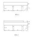
FIGS. 1-14 are perspective views illustrating a method for fabricating a device having metal gate transistors and a polysilicon resistor according to a preferred embodiment of the present invention.FIG. 15 illustrates a structural view of a semiconductor having metal gate transistors and a polysilicon resistor according to an embodiment of the present invention.- Referring to
FIGS. 1-14 ,FIGS. 1-14 are perspective views illustrating a method for fabricating a device having metal gate transistors and polysilicon resistor according to a preferred embodiment of the present invention. As shown inFIG. 1 , asubstrate 12 is first provided. Thesubstrate 12 is preferably a silicon substrate or a silicon-on-insulator (SOI) substrate. A transistor region and acapacitor region 18 are defined in thesubstrate 12, and a plurality ofshallow trench isolations 22 dividing the transistor region and thecapacitor region 18 is also formed. In this embodiment, the transistor region includes aNMOS transistor region 14 and aPMOS transistor region 16. - A gate
dielectric layer 24 composed of oxides is formed on thesubstrate 12, and apolysilicon layer 26 having a thickness of about 1000 angstroms is formed on the gatedielectric layer 24 thereafter. In this embodiment, thepolysilicon layer 26 can be composed of undoped polysilicon or polysilicon having n+ dopants, which are all within the scope of the present invention. - As shown in
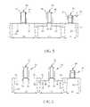
FIG. 2 , a patternedphotoresist 28 is formed on thepolysilicon layer 26, and an etching process is performed by using the patternedphotoresist 28 as a mask to remove a portion of thepolysilicon layer 26 disposed on theresistor region 18. Preferably, the portion of thepolysilicon layer 26 is removed by a dry etching process, and the removed portion of thepolysilicon layer 26 is approximately 200 angstroms. Nevertheless, other etching process (such as wet etching) can also be applied to remove a portion of thepolysilicon layer 26, and the thickness of the removed portion of thepolysilicon layer 26 could also be adjusted, which are all within the scope of the present invention. - As shown in
FIG. 3 , the patternedphotoresist 28 is removed, and ahardmask 30 is deposited on thepolysilicon layer 26. - As shown in
FIG. 4 , another patterned photoresist (not shown) is formed on thehardmask 30, and another etching process is conducted by using the patterned photoresist as a mask to form apolysilicon gate 32 in each of theNMOS transistor region 14 and thePMOS transistor region 16, and apolysilicon resistor 34 in theresistor region 18. Preferably, the channel length of thepolysilicon gate 32 in theNMOS transistor region 14 and thePMOS transistor region 16 is about 300 angstroms. It should also be noted that as a portion of thepolysilicon layer 26 in theresistor region 18 is removed in the previous step, the resultingpolysilicon resistor 34 would be lower in height than each of thepolysilicon gates 32, thereby creating a step height difference between the two structures. - According to an embodiment of the present invention, a single etching process or a two stage etching process could be used to form the
aforementioned polysilicon gates 32 and thepolysilicon resistor 34. For instance, a patterned photoresist (not shown) can be formed on thehardmask 30, and an etching process is performed by using the patterned photoresist as a mask to remove a portion of bothhardmask 30 and thepolysilicon layer 26, thereby forming thepolysilicon gates 32 and thepolysilicon resistor 34 within a single step. Alternatively, after a patterned photoresist (not shown) is formed on thehardmask 30, an etching process can be performed by using the patterned photoresist as a mask to remove only a portion of thehardmask 30. After the patterned photoresist is removed, another etching process is conducted by using theremaining hardmask 30 as a mask to etch the portion of thepolysilicon layer 26 not covered by thehardmask 30, thereby forming theaforementioned polysilicon gates 32 and thepolysilicon resistor 34. - As shown in
FIG. 5 , a light doping process is performed to form a plurality of lightly doped drains in theNMOS transistor region 14 and thePMOS transistor region 16. For instance, a patterned photoresist (not shown) is formed on regions outside theNMOS transistor region 14, and an ion implantation is performed by using the patterned photoresist as a mask to implant n-type dopants into thesubstrate 12 surrounding thepolysilicon gate 32 of theNMOS transistor region 14. This forms a lightly dopeddrain 36 in theNMOS transistor region 14. After the above patterned photoresist is stripped, another patterned photoresist is formed on regions outside thePMOS transistor region 16, and another ion implantation is conducted by using the patterned photoresist as a mask to implant p-type dopants into thesubstrate 12 surrounding thepolysilicon gate 32 of thePMOS transistor region 16. This forms a lightly dopeddrain 38 in thePMOS transistor region 38. - Next, a first stage spacer formation is conducted by depositing a
silicon nitride layer 42 and asilicon oxide layer 40 over the sidewall of thepolysilicon gate 32 in theNMOS transistor region 14 and thePMOS transistor region 16, and the sidewall of thepolysilicon resistor 34 in theresistor region 18. - A selective epitaxial growth (SEG) process is performed thereafter to form a strain silicon layer in the
substrate 12 of theNMOS transistor region 14 or thePMOS transistor region 16. For instance, after two recess (not shown) are formed in thesubstrate 12 surrounding thepolysilicon gate 32 of thePMOS transistor region 16, a SEG process is conducted to substantially fill the two recess with asilicon germanium layer 44. Thissilicon germanium layer 44 preferably provides a compressive strain to the channel region of thePMOS transistor region 16 and increases the hole transfer rate of the PMOS transistor. - Next, as shown in
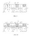
FIG. 6 , a series of heavily doped ion implantations are performed to form a source/drain region in each of theNMOS transistor region 14 and thePMOS transistor region 16. For instance, a patterned photoresist (not shown) is formed on regions outside theNMOS transistor region 14, and an ion implantation is conducted by using the patterned photoresist as a mask to implant n-type dopants into thesubstrate 12 surrounding thespacer 50 within theNMOS transistor region 14. This forms a source/drain region 52 in theNMOS transistor region 14. After stripping the patterned photoresist disposed on regions outside theNMOS transistor region 14, another patterned photoresist (not shown) is formed on regions outside thePMOS transistor region 16, and another ion implantation is conducted by using the patterned photoresist as a mask to implant p-type dopants into thesubstrate 12 surrounding thespacer 50 within thePMOS transistor region 16. This forms another source/drain region 54 in thePMOS transistor region 16. - After the formation of the source/
drain regions substrate 12 and thespacer 50. A rapid thermal annealing process is then performed by using high temperature to transform the metal layer disposed on thesubstrate 12 into asilicide layer 56. The unreacted metal layer is removed thereafter. - As shown in
FIG. 7 , asilicon oxide layer 58 and asilicon nitride layer 60 are deposited over the surface of thespacer 50 and thesubstrate 12. In this embodiment, the depth of thesilicon oxide layer 58 is about50 angstroms and the depth of thesilicon nitride layer 60 is about 100 angstroms. - As shown in
FIG. 8 , aninterlayer dielectric layer 62 composed of oxides is formed on thesilicon nitride layer 60 to cover theNMOS transistor region 14, thePMOS transistor region 16, and theresistor region 18. A chemical mechanical polishing process or a dry etching process is performed thereafter to remove a portion of theinterlayer dielectric layer 62. - According to the preferred embodiment of the present invention, the aforementioned chemical mechanical polishing process can be conducted by using the
hardmask 30 of different region as a stop layer to stop the chemical mechanical polishing process at different heights, such as having the polishing to stop directly at height A, stop directly at height B, or stop at height A and then to height B. For instance, the chemical mechanical polishing process can be performed by using thehardmask 30 of theNMOS transistor region 14 and thePMOS transistor region 16 as a stop layer to remove a portion of theinterlayer dielectric layer 62 and stop at thehardmask 30 of thetransistor regions 14,16 (such as height A). After the polishing process is completed, a metal gate formation process is performed to form metal gates in thetransistor regions - According to another embodiment of the present invention, after the polishing is stopped at height A, another polishing is performed by using the
hardmask 30 of theresistor region 18 as another stop layer to remove a portion of theinterlayer dielectric layer 62 and a portion of thepolysilicon gate 32 andspacer 50 of theNMOS transistor region 14 and thePMOS transistor region 16. This second polishing process would stop at thehardmask 30 of the resistor region18 (such as height B). - According to the third embodiment of the present invention, the chemical mechanical polishing process can be performed by using the
hardmask 30 of theresistor region 18 directly as a stop layer to remove a portion of thepolysilicon gate 32 andspacer 50 of theNMOS transistor region 14 and thePMOS transistor region 16 and stop at thehardmask 30 of the resistor region18 (such as height B). As shown inFIG. 9 , after the polishing process stops at height B and removes a portion of thepolysilicon gates 32 andspacer 50 of the transistor regions, a patterned photoresist (not shown) is used as a mask to perform an etching process to remove thepolysilicon gates 32 from theNMOS transistor region 14 and thePMOS transistor region 16 for forming anopening 64 in each transistor region. - As shown in
FIG. 10 , anoxide layer 66 is deposited in the bottom of eachopening 64, and adielectric layer 68 composed high-k dielectric material and an n-type metal layer 70 are disposed sequentially over the surface of theoxide layer 66 and theinterlayer dielectric layer 62. - As shown in
FIG. 11 , a patterned photoresist (not shown) is formed on areas outside thePMOS transistor region 16, and an etching process is conducted by using the patterned photoresist as a mask to remove the n-type metal layer 70 disposed on thePMOS transistor region 16. - As shown in
FIG. 12 , a p-type metal layer 72 is disposed over the surface of the n-type metal layer 70 and filled into eachopening 64. - As shown in
FIG. 13 , another chemical mechanical polishing process is conducted by using thehardmask 30 of theresistor region 18 as a stop layer to remove a portion of the p-type metal layer 72, the n-type metal layer 70,dielectric layer 68, and top of thespacer 50. - As shown in
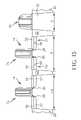
FIG. 14 , after removing thesilicon nitride layer 60 and thesilicon oxide layer 58, aNMOS transistor 76 and aPMOS transistor 78 are formed in theNMOS transistor region 14 and thePMOS transistor region 16 respectively, in which each of theNMOS transistor 76 and thePMOS transistor 78 includes a truncatedmetal gate structure 74. Each of the truncatedmetal gate structure 74 has a truncatedmetal gate 80 and atruncated spacer 82. Preferably, after the chemical mechanical polishing process performed previously, the top of thetruncated spacer 82 is substantially even with the top of thetruncated metal gate 80, and the top of thepolysilicon resistor 34 is also substantially even with top of each truncatedmetal gate structure 74. - According to another embodiment of the present invention, as shown in
FIG. 15 , after the polishing process shown inFIG. 8 stops at height A, a metal gate formation process is conducted thereafter to form another semiconductor device having metal gate transistor and polysilicon resistor. For instance, after the polishing process stops at height A, thehardmasks 30 of theNMOS transistor region 14 and thePMOS transistor region 16 are stripped, and the aforementioned process for forming metal gates is applied to deposit dielectric layer, n-type metal layer, and p-type metal layer to form another structure having a plurality ofmetal gate structures 84 and apolysilicon resistor 86. As shown inFIG. 15 , as themetal gate structures 84 within theNMOS transistor region 14 and thePMOS transistor region 16 are not partially removed during the chemical mechanical polishing process, the resulting height of thepolysilicon resistor 86 would be less than the height of themetal gate structures 84 of the transistor regions. - Overall, the present invention uses an etching process to remove a portion of the polysilicon layer within the resistor region, such that the surface of the polysilicon layer of the resistor region would be lower than the surface of the polysilicon layer of the surrounding transistor region. Next, a hardmask is formed over the surface of the polysilicon layer. As the height of the polysilicon layer in the resistor region is lower than the height of the polysilicon layer in the transistor region after the etching process, the polysilicon resistor fabricated thereafter would also be lower in height than the transistors in the transistor region. As a result, the hardmask disposed on the polysilicon resistor could be used as a stop layer to stop the later chemical mechanical polishing process on the surface of the polysilicon resistor, and the metal gate fabrication is conducted thereafter. By using this approach, the present invention could successfully fabricate a semiconductor device having both metal gate transistors and polysilicon resistor.
- Those skilled in the art will readily observe that numerous modifications and alterations of the device and method may be made while retaining the teachings of the invention.
Claims (19)
1. A method for fabricating metal gate transistors and a polysilicon resistor, comprising:
providing a substrate having a transistor region and a resistor region;
forming a polysilicon layer on the substrate to cover the transistor region and the resistor region;
removing a portion of the polysilicon layer disposed in the resistor region;
patterning the polysilicon layer for creating a step height between the surface of the polysilicon layer disposed in the transistor region and the surface of the polysilicon layer disposed in the resistor region;
forming at least one polysilicon gate in the transistor region and one polysilicon resistor in the resistor region; and
forming the polysilicon gate into a metal gate transistor.
2. The method for fabricating metal gate transistors and a polysilicon resistor ofclaim 1 , wherein the step of forming at least one polysilicon gate in the transistor region and one polysilicon resistor in the resistor region further comprises:
forming a hardmask on the polysilicon layer after removing the portion of the polysilicon layer disposed in the resistor region;
patterning the hardmask and the polysilicon layer to form a first polysilicon gate and a second polysilicon gate in the transistor region and the polysilicon resistor in the resistor region;
forming a lightly doped drain in the substrate surrounding the first polysilicon gate and the second polysilicon gate;
forming a spacer on the sidewall of each of the first polysilicon gate, the second polysilicon gate, and the polysilicon resistor;
forming a source/drain region in the substrate surrounding the spacer disposed in the transistor region;
performing a salicide process to form a silicide layer on the surface of the substrate surrounding the spacer disposed in the transistor region;
forming an interlayer dielectric layer on the silicon nitride layer;
performing a first removal process to remove a portion of the interlayer dielectric layer and expose the hardmask.
3. The method for fabricating metal gate transistors and a polysilicon resistor ofclaim 2 , wherein the step of forming the polysilicon gate into the metal gate transistor further comprises:
removing the first polysilicon gate and the second polysilicon gate to form a first opening and a second opening in the interlayer dielectric layer;
depositing a first metal layer in the first opening and the second opening;
removing the first metal layer from the second opening;
filling the first opening and the second opening with a second metal layer; and
performing a second removal process to remove a portion of the first metal layer and the second metal layer for forming a first metal gate transistor and a second metal gate transistor in the transistor region.
4. The method for fabricating metal gate transistors and a polysilicon resistor ofclaim 2 , wherein the first metal gate transistor is a NMOS transistor and the second metal gate transistor is a PMOS transistor.
5. The method for fabricating metal gate transistors and a polysilicon resistor ofclaim 4 , further comprising forming a silicon germanium layer in the substrate surrounding the gate before forming the spacer.
6. The method for fabricating metal gate transistors and a polysilicon resistor ofclaim 2 , wherein the first removal process is performed until reaching the surface of the hardmask of the transistor region.
7. The method for fabricating metal gate transistors and a polysilicon resistor ofclaim 2 , wherein the first removal process is performed until reaching the surface of the hardmask of the resistor region, wherein the first removal process comprises a chemical mechanical polishing process or an etching process.
8. The method for fabricating metal gate transistors and a polysilicon resistor ofclaim 7 , wherein the first removal process further comprises:
removing a portion of the interlayer dielectric layer until reaching the surface of the hardmask of the transistor region; and
using the hardmask of the resistor region as a stop layer to remove a portion of the first polysilicon gate, a portion of the second polysilicon gate, and a portion of the spacer until reaching the surface of the hardmask of the resistor region.
9. The method for fabricating metal gate transistors and a polysilicon resistor ofclaim 8 further comprising utilizing an etching process or a chemical mechanical polishing process to remove the interlayer dielectric layer, the first polysilicon gate, and the second polysilicon gate.
10. A semiconductor device having metal gate transistor and polysilicon resistor, comprising:
a substrate having a transistor region and a resistor region;
a transistor disposed in the transistor region, wherein the transistor comprises at least a metal gate structure; and
a polysilicon resistor structure disposed in the resistor region, wherein the height of the polysilicon resistor structure is less than the height of the metal gate structure.
11. The semiconductor device having metal gate transistor and polysilicon resistor ofclaim 10 , wherein the metal gate structure further comprises:
a metal gate disposed in the transistor region; and
a first spacer disposed around the sidewall of the metal gate.
12. The semiconductor device having metal gate transistor and polysilicon resistor ofclaim 10 , wherein the transistor is a NMOS transistor or a PMOS transistor.
13. The semiconductor device having metal gate transistor and polysilicon resistor ofclaim 12 , further comprising a silicon germanium layer disposed in the substrate surrounding the metal gate structure of the PMOS transistor.
14. The semiconductor device having metal gate transistor and polysilicon resistor ofclaim 10 , further comprising a silicide layer disposed in the substrate surrounding the metal gate structure.
15. The semiconductor device having metal gate transistor and polysilicon resistor ofclaim 10 , further comprising an interlayer dielectric layer disposed on the transistor and the polysilicon resistor structure.
16. The semiconductor device having metal gate transistor and polysilicon resistor ofclaim 10 , wherein the polysilicon resistor structure further comprises:
a polysilicon resistor, disposed in the resistor region; and
a second spacer disposed around the sidewall of the polysilicon resistor.
17. A semiconductor device having metal gate transistor and polysilicon resistor, comprising:
a substrate having a transistor region and a resistor region;
a transistor disposed in the transistor region, wherein the transistor comprises at least a truncated metal gate structure; and
a polysilicon resistor structure disposed in the resistor region, wherein the top of the polysilicon resistor structure is even with the top of the truncated metal gate structure.
18. The semiconductor device having metal gate transistor and polysilicon resistor ofclaim 17 , wherein the truncated metal gate structure further comprises:
a truncated metal gate; and
a truncated spacer disposed around the sidewall of the truncated metal gate, wherein the top of the truncated spacer is even with the top of the truncated metal gate.
19. The semiconductor device having metal gate transistor and polysilicon resistor ofclaim 17 , wherein the polysilicon resistor structure further comprises:
a polysilicon resistor, disposed in the resistor region; and
a spacer disposed around the sidewall of the polysilicon resistor.
Priority Applications (1)
| Application Number | Priority Date | Filing Date | Title |
|---|---|---|---|
| US12/052,728US7932146B2 (en) | 2008-03-20 | 2008-03-20 | Metal gate transistor and polysilicon resistor and method for fabricating the same |
Applications Claiming Priority (1)
| Application Number | Priority Date | Filing Date | Title |
|---|---|---|---|
| US12/052,728US7932146B2 (en) | 2008-03-20 | 2008-03-20 | Metal gate transistor and polysilicon resistor and method for fabricating the same |
Publications (2)
| Publication Number | Publication Date |
|---|---|
| US20090236669A1true US20090236669A1 (en) | 2009-09-24 |
| US7932146B2 US7932146B2 (en) | 2011-04-26 |
Family
ID=41088010
Family Applications (1)
| Application Number | Title | Priority Date | Filing Date |
|---|---|---|---|
| US12/052,728Active2029-07-06US7932146B2 (en) | 2008-03-20 | 2008-03-20 | Metal gate transistor and polysilicon resistor and method for fabricating the same |
Country Status (1)
| Country | Link |
|---|---|
| US (1) | US7932146B2 (en) |
Cited By (33)
| Publication number | Priority date | Publication date | Assignee | Title |
|---|---|---|---|---|
| US20090218636A1 (en)* | 2008-02-29 | 2009-09-03 | Chartered Semiconductor Manufacturing Ltd. | Integrated circuit system for suppressing short channel effects |
| US20100025772A1 (en)* | 2008-07-31 | 2010-02-04 | Andreas Kurz | Semiconductor device comprising a silicon/germanium resistor |
| US20100038692A1 (en)* | 2008-08-14 | 2010-02-18 | Harry Chuang | Integrating the Formation of I/O and Core MOS Devices with MOS Capacitors and Resistors |
| US20100237435A1 (en)* | 2009-03-17 | 2010-09-23 | International Business Machines Corporation | Method and structure for gate height scaling with high-k/metal gate technology |
| US20100320544A1 (en)* | 2009-06-22 | 2010-12-23 | Chih-Yu Tseng | Metal gate transistor and resistor and method for fabricating the same |
| US20100327370A1 (en)* | 2009-06-26 | 2010-12-30 | Chia-Hong Jan | Non-planar embedded polysilicon resistor |
| DE102009047306A1 (en)* | 2009-11-30 | 2011-06-01 | Globalfoundries Dresden Module One Limited Liability Company & Co. Kg | High-k metal gate electrode structures made by separately removing dummy materials using a masking scheme prior to gate patterning |
| US20110156162A1 (en)* | 2009-12-31 | 2011-06-30 | Ralf Richter | Semiconductor resistors formed at a lower height level in a semiconductor device comprising metal gates |
| US20110189827A1 (en)* | 2010-02-04 | 2011-08-04 | Che-Hua Hsu | Method of fabricating efuse structure, resistor sturcture and transistor sturcture |
| US20110266633A1 (en)* | 2010-04-30 | 2011-11-03 | Globalfoundries Inc. | Semiconductor Device Comprising Metal Gates and Semiconductor Resistors Formed on the Basis of a Replacement Gate Approach |
| CN102376538A (en)* | 2010-08-04 | 2012-03-14 | 台湾积体电路制造股份有限公司 | Method of forming polysilicon resistor device and semiconductor device |
| US20120088358A1 (en)* | 2010-10-06 | 2012-04-12 | Jong-Won Lee | Methods of Forming Gates of Semiconductor Devices |
| US20120217586A1 (en)* | 2011-02-25 | 2012-08-30 | Taiwan Semiconductor Manufacturing Company, Ltd. | Integrated circuits with resistors and methods of forming the same |
| US20120319209A1 (en)* | 2011-06-16 | 2012-12-20 | Renesas Electronics Corporation | Semiconductor Device Having Mixedly Mounted Components with Common Film Layers and Method of Manufacturing the Same |
| US20130095644A1 (en)* | 2011-10-18 | 2013-04-18 | Taiwan Semiconductor Manufacturing Company, Ltd., ("Tsmc") | Planarization process for semiconductor device fabrication |
| CN103137657A (en)* | 2011-11-25 | 2013-06-05 | 中芯国际集成电路制造(上海)有限公司 | Semiconductor integrated device and forming method thereof |
| CN103165466A (en)* | 2011-12-16 | 2013-06-19 | 台湾积体电路制造股份有限公司 | Semiconductor device including polysilicon resistor and metal gate resistor and methods of fabricating thereof |
| US8519487B2 (en) | 2011-03-21 | 2013-08-27 | United Microelectronics Corp. | Semiconductor device |
| US8524556B1 (en) | 2012-03-14 | 2013-09-03 | United Microelectronics Corp. | Resistor and manufacturing method thereof |
| US20130228878A1 (en)* | 2012-03-02 | 2013-09-05 | Taiwan Semiconductor Manufacturing Company, Ltd. | Poly resistor design for replacement gate technology |
| US8598028B2 (en)* | 2011-12-22 | 2013-12-03 | Taiwan Semiconductor Manufacturing Company, Ltd. | Gate height loss improvement for a transistor |
| CN103872048A (en)* | 2012-12-17 | 2014-06-18 | 德州仪器公司 | Integrated circuit and forming method thereof |
| US20140295660A1 (en)* | 2012-05-14 | 2014-10-02 | United Microelectronics Corp. | Method of forming semiconductor device |
| US20140327080A1 (en)* | 2013-05-02 | 2014-11-06 | United Microelectronics Corp. | Semiconductor structure and manufacturing method thereof |
| TWI493658B (en)* | 2009-11-18 | 2015-07-21 | United Microelectronics Corp | Method of fabricating efuse, resistor and transistor |
| US20150214114A1 (en)* | 2014-01-28 | 2015-07-30 | United Microelectronics Corp. | Manufacturing method of semiconductor structure |
| US9153684B2 (en) | 2009-10-30 | 2015-10-06 | Globalfoundries Inc. | Semiconductor fuses in a semiconductor device comprising metal gates |
| US20160351451A1 (en)* | 2011-11-22 | 2016-12-01 | Taiwan Semiconductor Manufacturing Company, Ltd. | Methods and Apparatus for MOS Capacitors in Replacement Gate Process |
| TWI584433B (en)* | 2013-04-30 | 2017-05-21 | 聯華電子股份有限公司 | Semiconductor structure and manufacturing method thereof |
| US20170352548A1 (en)* | 2014-03-13 | 2017-12-07 | Taiwan Semiconductor Manufacturing Co., Ltd. | Cmp-friendly coatings for planar recessing or removing of variable-height layers |
| US10263012B2 (en)* | 2011-10-11 | 2019-04-16 | Renesas Electronics Corporation | Semiconductor integrated circuit device comprising MISFETs in SOI and bulk substrate regions |
| US10263005B2 (en)* | 2013-02-12 | 2019-04-16 | Renesas Electronics Corporation | Method of manufacturing a semiconductor device |
| CN116799004A (en)* | 2023-08-23 | 2023-09-22 | 合肥晶合集成电路股份有限公司 | Semiconductor integrated device and manufacturing method thereof |
Families Citing this family (33)
| Publication number | Priority date | Publication date | Assignee | Title |
|---|---|---|---|---|
| JP4458129B2 (en)* | 2007-08-09 | 2010-04-28 | ソニー株式会社 | Semiconductor device and manufacturing method thereof |
| US7838946B2 (en)* | 2008-03-28 | 2010-11-23 | United Microelectronics Corp. | Method for fabricating semiconductor structure and structure of static random access memory |
| US8350337B2 (en)* | 2009-12-29 | 2013-01-08 | United Microelectronics Corp. | Semiconductor device and method of forming the same |
| US8399310B2 (en) | 2010-10-29 | 2013-03-19 | Freescale Semiconductor, Inc. | Non-volatile memory and logic circuit process integration |
| US9524934B2 (en)* | 2011-11-22 | 2016-12-20 | Taiwan Semiconductor Manufacturing Company, Ltd. | Integrated circuits with electrical fuses and methods of forming the same |
| US8906764B2 (en) | 2012-01-04 | 2014-12-09 | Freescale Semiconductor, Inc. | Non-volatile memory (NVM) and logic integration |
| US8951863B2 (en) | 2012-04-06 | 2015-02-10 | Freescale Semiconductor, Inc. | Non-volatile memory (NVM) and logic integration |
| US9087913B2 (en) | 2012-04-09 | 2015-07-21 | Freescale Semiconductor, Inc. | Integration technique using thermal oxide select gate dielectric for select gate and apartial replacement gate for logic |
| US8404544B1 (en)* | 2012-04-13 | 2013-03-26 | Taiwan Semiconductor Manufacturing Company, Ltd. | Fabrication methods of integrated semiconductor structure |
| US9219059B2 (en) | 2012-09-26 | 2015-12-22 | International Business Machines Corporation | Semiconductor structure with integrated passive structures |
| US9111865B2 (en) | 2012-10-26 | 2015-08-18 | Freescale Semiconductor, Inc. | Method of making a logic transistor and a non-volatile memory (NVM) cell |
| KR102070094B1 (en) | 2012-12-13 | 2020-01-29 | 삼성전자주식회사 | Semiconductor Device Having a Resistor Electrode |
| US9006093B2 (en) | 2013-06-27 | 2015-04-14 | Freescale Semiconductor, Inc. | Non-volatile memory (NVM) and high voltage transistor integration |
| US8871598B1 (en) | 2013-07-31 | 2014-10-28 | Freescale Semiconductor, Inc. | Non-volatile memory (NVM) and high-k and metal gate integration using gate-first methodology |
| US9129996B2 (en) | 2013-07-31 | 2015-09-08 | Freescale Semiconductor, Inc. | Non-volatile memory (NVM) cell and high-K and metal gate transistor integration |
| US8877585B1 (en) | 2013-08-16 | 2014-11-04 | Freescale Semiconductor, Inc. | Non-volatile memory (NVM) cell, high voltage transistor, and high-K and metal gate transistor integration |
| US9082837B2 (en) | 2013-08-08 | 2015-07-14 | Freescale Semiconductor, Inc. | Nonvolatile memory bitcell with inlaid high k metal select gate |
| US9252246B2 (en) | 2013-08-21 | 2016-02-02 | Freescale Semiconductor, Inc. | Integrated split gate non-volatile memory cell and logic device |
| US9082650B2 (en) | 2013-08-21 | 2015-07-14 | Freescale Semiconductor, Inc. | Integrated split gate non-volatile memory cell and logic structure |
| US8932925B1 (en) | 2013-08-22 | 2015-01-13 | Freescale Semiconductor, Inc. | Split-gate non-volatile memory (NVM) cell and device structure integration |
| US9275864B2 (en) | 2013-08-22 | 2016-03-01 | Freescale Semiconductor,Inc. | Method to form a polysilicon nanocrystal thin film storage bitcell within a high k metal gate platform technology using a gate last process to form transistor gates |
| US9111867B2 (en) | 2013-08-30 | 2015-08-18 | Freescale Semiconductor, Inc. | Split gate nanocrystal memory integration |
| US9129855B2 (en) | 2013-09-30 | 2015-09-08 | Freescale Semiconductor, Inc. | Non-volatile memory (NVM) and high-k and metal gate integration using gate-first methodology |
| US8901632B1 (en) | 2013-09-30 | 2014-12-02 | Freescale Semiconductor, Inc. | Non-volatile memory (NVM) and high-K and metal gate integration using gate-last methodology |
| US9136129B2 (en) | 2013-09-30 | 2015-09-15 | Freescale Semiconductor, Inc. | Non-volatile memory (NVM) and high-k and metal gate integration using gate-last methodology |
| US9231077B2 (en) | 2014-03-03 | 2016-01-05 | Freescale Semiconductor, Inc. | Method of making a logic transistor and non-volatile memory (NVM) cell |
| US9472418B2 (en) | 2014-03-28 | 2016-10-18 | Freescale Semiconductor, Inc. | Method for forming a split-gate device |
| US9252152B2 (en) | 2014-03-28 | 2016-02-02 | Freescale Semiconductor, Inc. | Method for forming a split-gate device |
| US9112056B1 (en) | 2014-03-28 | 2015-08-18 | Freescale Semiconductor, Inc. | Method for forming a split-gate device |
| US9379222B2 (en) | 2014-05-30 | 2016-06-28 | Freescale Semiconductor, Inc. | Method of making a split gate non-volatile memory (NVM) cell |
| US9257445B2 (en) | 2014-05-30 | 2016-02-09 | Freescale Semiconductor, Inc. | Method of making a split gate non-volatile memory (NVM) cell and a logic transistor |
| US9343314B2 (en) | 2014-05-30 | 2016-05-17 | Freescale Semiconductor, Inc. | Split gate nanocrystal memory integration |
| US11107902B2 (en) | 2018-06-25 | 2021-08-31 | Taiwan Semiconductor Manufacturing Company, Ltd. | Dielectric spacer to prevent contacting shorting |
Citations (8)
| Publication number | Priority date | Publication date | Assignee | Title |
|---|---|---|---|---|
| US5141597A (en)* | 1990-11-14 | 1992-08-25 | United Technologies Corporation | Thin polysilicon resistors |
| US6207543B1 (en)* | 1997-06-30 | 2001-03-27 | Vlsi Technology, Inc. | Metallization technique for gate electrodes and local interconnects |
| US6509225B2 (en)* | 1998-12-25 | 2003-01-21 | Matsushita Electric Industrial Co., Ltd. | Semiconductor device and method of manufacturing the same |
| US6768174B2 (en)* | 2001-09-07 | 2004-07-27 | Seiko Instruments Inc. | Complementary MOS transistors having p-type gate electrodes |
| US6936520B2 (en)* | 2002-10-31 | 2005-08-30 | Fujitsu Limited | Method for fabricating semiconductor device having gate electrode together with resistance element |
| US20050191833A1 (en)* | 2004-02-27 | 2005-09-01 | Samsung Electronics Co., Ltd. | Method of fabricating MOS transistor having fully silicided gate |
| US20070184600A1 (en)* | 2006-02-06 | 2007-08-09 | Freescale Semiconductor | Stressed-channel CMOS transistors |
| US20090039433A1 (en)* | 2007-08-08 | 2009-02-12 | Taiwan Semiconductor Manufacturing Company, Ltd. | Semiconductor device with high-k/dual metal gate |
Family Cites Families (2)
| Publication number | Priority date | Publication date | Assignee | Title |
|---|---|---|---|---|
| JP3025478B2 (en) | 1998-07-13 | 2000-03-27 | 松下電器産業株式会社 | Semiconductor device and manufacturing method thereof |
| CN1277296C (en) | 2003-03-27 | 2006-09-27 | 台湾积体电路制造股份有限公司 | Field effect transistor structure possessing strain silicon germanium layer beaping crystal and its manufacturing method |
- 2008
- 2008-03-20USUS12/052,728patent/US7932146B2/enactiveActive
Patent Citations (8)
| Publication number | Priority date | Publication date | Assignee | Title |
|---|---|---|---|---|
| US5141597A (en)* | 1990-11-14 | 1992-08-25 | United Technologies Corporation | Thin polysilicon resistors |
| US6207543B1 (en)* | 1997-06-30 | 2001-03-27 | Vlsi Technology, Inc. | Metallization technique for gate electrodes and local interconnects |
| US6509225B2 (en)* | 1998-12-25 | 2003-01-21 | Matsushita Electric Industrial Co., Ltd. | Semiconductor device and method of manufacturing the same |
| US6768174B2 (en)* | 2001-09-07 | 2004-07-27 | Seiko Instruments Inc. | Complementary MOS transistors having p-type gate electrodes |
| US6936520B2 (en)* | 2002-10-31 | 2005-08-30 | Fujitsu Limited | Method for fabricating semiconductor device having gate electrode together with resistance element |
| US20050191833A1 (en)* | 2004-02-27 | 2005-09-01 | Samsung Electronics Co., Ltd. | Method of fabricating MOS transistor having fully silicided gate |
| US20070184600A1 (en)* | 2006-02-06 | 2007-08-09 | Freescale Semiconductor | Stressed-channel CMOS transistors |
| US20090039433A1 (en)* | 2007-08-08 | 2009-02-12 | Taiwan Semiconductor Manufacturing Company, Ltd. | Semiconductor device with high-k/dual metal gate |
Cited By (72)
| Publication number | Priority date | Publication date | Assignee | Title |
|---|---|---|---|---|
| US20090218636A1 (en)* | 2008-02-29 | 2009-09-03 | Chartered Semiconductor Manufacturing Ltd. | Integrated circuit system for suppressing short channel effects |
| US7867835B2 (en)* | 2008-02-29 | 2011-01-11 | Chartered Semiconductor Manufacturing Ltd. | Integrated circuit system for suppressing short channel effects |
| US8193066B2 (en)* | 2008-07-31 | 2012-06-05 | Globalfoundries Inc. | Semiconductor device comprising a silicon/germanium resistor |
| US20100025772A1 (en)* | 2008-07-31 | 2010-02-04 | Andreas Kurz | Semiconductor device comprising a silicon/germanium resistor |
| US20100038692A1 (en)* | 2008-08-14 | 2010-02-18 | Harry Chuang | Integrating the Formation of I/O and Core MOS Devices with MOS Capacitors and Resistors |
| US8728900B2 (en) | 2008-08-14 | 2014-05-20 | Taiwan Semiconductor Manufacturing Company, Ltd. | Integrating the formation of I/O and core MOS devices with MOS capacitors and resistors |
| US8294216B2 (en)* | 2008-08-14 | 2012-10-23 | Taiwan Semiconductor Manufacturing Company, Ltd. | Integrating the formation of I/O and core MOS devices with MOS capacitors and resistors |
| US20100237435A1 (en)* | 2009-03-17 | 2010-09-23 | International Business Machines Corporation | Method and structure for gate height scaling with high-k/metal gate technology |
| US8227870B2 (en)* | 2009-03-17 | 2012-07-24 | International Business Machines Corporation | Method and structure for gate height scaling with high-k/metal gate technology |
| US20120126335A1 (en)* | 2009-03-17 | 2012-05-24 | International Business Machines Corporation | Method and structure for gate height scaling with high-k/metal gate technology |
| US8138037B2 (en) | 2009-03-17 | 2012-03-20 | International Business Machines Corporation | Method and structure for gate height scaling with high-k/metal gate technology |
| US20110171810A1 (en)* | 2009-06-22 | 2011-07-14 | Chih-Yu Tseng | Metal gate transistor and resistor and method for fabricating the same |
| US8252657B2 (en) | 2009-06-22 | 2012-08-28 | United Microelectronics Corp. | Metal gate transistor and resistor and method for fabricating the same |
| US7994576B2 (en) | 2009-06-22 | 2011-08-09 | United Microelectronics Corp. | Metal gate transistor and resistor and method for fabricating the same |
| US20100320544A1 (en)* | 2009-06-22 | 2010-12-23 | Chih-Yu Tseng | Metal gate transistor and resistor and method for fabricating the same |
| US20100327370A1 (en)* | 2009-06-26 | 2010-12-30 | Chia-Hong Jan | Non-planar embedded polysilicon resistor |
| US9153684B2 (en) | 2009-10-30 | 2015-10-06 | Globalfoundries Inc. | Semiconductor fuses in a semiconductor device comprising metal gates |
| TWI493658B (en)* | 2009-11-18 | 2015-07-21 | United Microelectronics Corp | Method of fabricating efuse, resistor and transistor |
| US8652956B2 (en) | 2009-11-30 | 2014-02-18 | Globalfoundries Inc. | High-k metal gate electrode structures formed by separate removal of placeholder materials using a masking regime prior to gate patterning |
| DE102009047306B4 (en)* | 2009-11-30 | 2015-02-12 | Globalfoundries Dresden Module One Limited Liability Company & Co. Kg | A method of fabricating gate electrode structures by separately removing dummy materials using a masking scheme prior to gate patterning |
| DE102009047306A1 (en)* | 2009-11-30 | 2011-06-01 | Globalfoundries Dresden Module One Limited Liability Company & Co. Kg | High-k metal gate electrode structures made by separately removing dummy materials using a masking scheme prior to gate patterning |
| US8232188B2 (en) | 2009-11-30 | 2012-07-31 | Globalfoundries Inc. | High-K metal gate electrode structures formed by separate removal of placeholder materials using a masking regime prior to gate patterning |
| US8658509B2 (en)* | 2009-12-31 | 2014-02-25 | Globalfoundries Inc. | Semiconductor resistors formed at a lower height level in a semiconductor device comprising metal gates |
| US20110156162A1 (en)* | 2009-12-31 | 2011-06-30 | Ralf Richter | Semiconductor resistors formed at a lower height level in a semiconductor device comprising metal gates |
| DE102009055437B4 (en)* | 2009-12-31 | 2017-08-10 | Globalfoundries Dresden Module One Limited Liability Company & Co. Kg | Semiconductor resistors fabricated in a semiconductor device having metal gate structures at a lower level, and methods of fabricating the semiconductor resistors |
| DE102009055437A1 (en)* | 2009-12-31 | 2011-07-07 | GLOBALFOUNDRIES Dresden Module One Limited Liability Company & Co. KG, 01109 | Semiconductor resistors made in a semiconductor device with Metallgatestrukturen at a lower level |
| US20110189827A1 (en)* | 2010-02-04 | 2011-08-04 | Che-Hua Hsu | Method of fabricating efuse structure, resistor sturcture and transistor sturcture |
| US8003461B1 (en)* | 2010-02-04 | 2011-08-23 | United Microelectronics Corp. | Method of fabricating efuse structure, resistor sturcture and transistor sturcture |
| US8450163B2 (en)* | 2010-04-30 | 2013-05-28 | Globalfoundries Inc. | Semiconductor device comprising metal gates and semiconductor resistors formed on the basis of a replacement gate approach |
| US20110266633A1 (en)* | 2010-04-30 | 2011-11-03 | Globalfoundries Inc. | Semiconductor Device Comprising Metal Gates and Semiconductor Resistors Formed on the Basis of a Replacement Gate Approach |
| CN102376538A (en)* | 2010-08-04 | 2012-03-14 | 台湾积体电路制造股份有限公司 | Method of forming polysilicon resistor device and semiconductor device |
| KR101777662B1 (en) | 2010-10-06 | 2017-09-14 | 삼성전자 주식회사 | Method for forming gate of semiconductor device |
| US20120088358A1 (en)* | 2010-10-06 | 2012-04-12 | Jong-Won Lee | Methods of Forming Gates of Semiconductor Devices |
| US8962415B2 (en) | 2010-10-06 | 2015-02-24 | Samsung Electronics Co., Ltd. | Methods of forming gates of semiconductor devices |
| US8735250B2 (en)* | 2010-10-06 | 2014-05-27 | Samsung Electronics Co., Ltd. | Methods of forming gates of semiconductor devices |
| US8835246B2 (en)* | 2011-02-25 | 2014-09-16 | Taiwan Semiconductor Manufacturing Company, Ltd. | Integrated circuits with resistors and methods of forming the same |
| US20120217586A1 (en)* | 2011-02-25 | 2012-08-30 | Taiwan Semiconductor Manufacturing Company, Ltd. | Integrated circuits with resistors and methods of forming the same |
| US9171839B2 (en) | 2011-02-25 | 2015-10-27 | Taiwan Semiconductor Manufacturing Company, Ltd. | Integrated circuits with resistors |
| US9887189B2 (en) | 2011-02-25 | 2018-02-06 | Taiwan Semiconductor Manufacturing Company, Ltd. | Integrated circuits with resistors |
| US8723274B2 (en) | 2011-03-21 | 2014-05-13 | United Microelectronics Corp. | Semiconductor device and method for fabricating the same |
| US8519487B2 (en) | 2011-03-21 | 2013-08-27 | United Microelectronics Corp. | Semiconductor device |
| US9070564B2 (en) | 2011-06-16 | 2015-06-30 | Renesas Electronics Corporation | Semiconductor device having mixedly mounted components with common film layers and method of manufacturing the same |
| US20120319209A1 (en)* | 2011-06-16 | 2012-12-20 | Renesas Electronics Corporation | Semiconductor Device Having Mixedly Mounted Components with Common Film Layers and Method of Manufacturing the Same |
| US8823112B2 (en)* | 2011-06-16 | 2014-09-02 | Renesas Electronics Corporation | Semiconductor device having mixedly mounted components with common film layers and method of manufacturing the same |
| US10263012B2 (en)* | 2011-10-11 | 2019-04-16 | Renesas Electronics Corporation | Semiconductor integrated circuit device comprising MISFETs in SOI and bulk substrate regions |
| US20130095644A1 (en)* | 2011-10-18 | 2013-04-18 | Taiwan Semiconductor Manufacturing Company, Ltd., ("Tsmc") | Planarization process for semiconductor device fabrication |
| US8975179B2 (en)* | 2011-10-18 | 2015-03-10 | Taiwan Semiconductor Manufacturing Company, Ltd. | Planarization process for semiconductor device fabrication |
| US10720361B2 (en) | 2011-11-22 | 2020-07-21 | Taiwan Semiconductor Manufacturing Company | Methods and apparatus for MOS capacitors in replacement gate process |
| US10354920B2 (en)* | 2011-11-22 | 2019-07-16 | Taiwan Semiconductor Manufacturing Company | Methods and apparatus for MOS capacitors in replacement gate process |
| US20160351451A1 (en)* | 2011-11-22 | 2016-12-01 | Taiwan Semiconductor Manufacturing Company, Ltd. | Methods and Apparatus for MOS Capacitors in Replacement Gate Process |
| CN103137657A (en)* | 2011-11-25 | 2013-06-05 | 中芯国际集成电路制造(上海)有限公司 | Semiconductor integrated device and forming method thereof |
| CN103165466A (en)* | 2011-12-16 | 2013-06-19 | 台湾积体电路制造股份有限公司 | Semiconductor device including polysilicon resistor and metal gate resistor and methods of fabricating thereof |
| US9070624B2 (en)* | 2011-12-16 | 2015-06-30 | Taiwan Semiconductor Manufacturing Company, Ltd. | Semiconductor device including polysilicon resistor and metal gate resistor and methods of fabricating thereof |
| US20130157452A1 (en)* | 2011-12-16 | 2013-06-20 | Taiwan Semiconductor Manufacturing Company, Ltd. ("Tsmc") | Semiconductor device including polysilicon resistor and metal gate resistor and methods of fabricating thereof |
| US8598028B2 (en)* | 2011-12-22 | 2013-12-03 | Taiwan Semiconductor Manufacturing Company, Ltd. | Gate height loss improvement for a transistor |
| US20130228878A1 (en)* | 2012-03-02 | 2013-09-05 | Taiwan Semiconductor Manufacturing Company, Ltd. | Poly resistor design for replacement gate technology |
| US8524556B1 (en) | 2012-03-14 | 2013-09-03 | United Microelectronics Corp. | Resistor and manufacturing method thereof |
| US8692334B2 (en) | 2012-03-14 | 2014-04-08 | United Microelectronics Corp. | Resistor integrated with transistor having metal gate |
| US9006091B2 (en)* | 2012-05-14 | 2015-04-14 | United Microelectronics Corp. | Method of forming semiconductor device having metal gate |
| US20140295660A1 (en)* | 2012-05-14 | 2014-10-02 | United Microelectronics Corp. | Method of forming semiconductor device |
| US8877623B2 (en)* | 2012-05-14 | 2014-11-04 | United Microelectronics Corp. | Method of forming semiconductor device |
| US8927385B2 (en)* | 2012-12-17 | 2015-01-06 | Texas Instruments Incorporated | ZTCR poly resistor in replacement gate flow |
| CN103872048A (en)* | 2012-12-17 | 2014-06-18 | 德州仪器公司 | Integrated circuit and forming method thereof |
| US10263005B2 (en)* | 2013-02-12 | 2019-04-16 | Renesas Electronics Corporation | Method of manufacturing a semiconductor device |
| TWI584433B (en)* | 2013-04-30 | 2017-05-21 | 聯華電子股份有限公司 | Semiconductor structure and manufacturing method thereof |
| US9331171B2 (en) | 2013-05-02 | 2016-05-03 | United Microelectronics Corp. | Manufacturing method for forming semiconductor structure |
| US9147747B2 (en)* | 2013-05-02 | 2015-09-29 | United Microelectronics Corp. | Semiconductor structure with hard mask disposed on the gate structure |
| US20140327080A1 (en)* | 2013-05-02 | 2014-11-06 | United Microelectronics Corp. | Semiconductor structure and manufacturing method thereof |
| US20150214114A1 (en)* | 2014-01-28 | 2015-07-30 | United Microelectronics Corp. | Manufacturing method of semiconductor structure |
| US20170352548A1 (en)* | 2014-03-13 | 2017-12-07 | Taiwan Semiconductor Manufacturing Co., Ltd. | Cmp-friendly coatings for planar recessing or removing of variable-height layers |
| US11011385B2 (en)* | 2014-03-13 | 2021-05-18 | Taiwan Semiconductor Manufacturing Co., Ltd. | CMP-friendly coatings for planar recessing or removing of variable-height layers |
| CN116799004A (en)* | 2023-08-23 | 2023-09-22 | 合肥晶合集成电路股份有限公司 | Semiconductor integrated device and manufacturing method thereof |
Also Published As
| Publication number | Publication date |
|---|---|
| US7932146B2 (en) | 2011-04-26 |
Similar Documents
| Publication | Publication Date | Title |
|---|---|---|
| US7932146B2 (en) | Metal gate transistor and polysilicon resistor and method for fabricating the same | |
| US7888195B2 (en) | Metal gate transistor and method for fabricating the same | |
| US7994576B2 (en) | Metal gate transistor and resistor and method for fabricating the same | |
| US8404535B2 (en) | Metal gate transistor and method for fabricating the same | |
| US6939751B2 (en) | Method and manufacture of thin silicon on insulator (SOI) with recessed channel | |
| US8106456B2 (en) | SOI transistors having an embedded extension region to improve extension resistance and channel strain characteristics | |
| US9502413B2 (en) | Semiconductor devices including raised source/drain stressors and methods of manufacturing the same | |
| US9312179B2 (en) | Method of making a finFET, and finFET formed by the method | |
| US8637936B2 (en) | Metal gate transistor with resistor | |
| US20070134859A1 (en) | Strained silicon MOS device with box layer between the source and drain regions | |
| JP4119663B2 (en) | CMOS structure and fabrication method with non-epitaxial raised source / drain and self-aligned gate | |
| US8980753B2 (en) | Metal gate transistor and method for fabricating the same | |
| CN101552229B (en) | Semiconductor element and manufacturing method thereof | |
| US7009258B2 (en) | Method of building a CMOS structure on thin SOI with source/drain electrodes formed by in situ doped selective amorphous silicon | |
| JP2006511083A (en) | Manufacturing method of semiconductor device and semiconductor device obtained by such method | |
| JP2009117621A (en) | Semiconductor device and manufacturing method thereof | |
| US7338910B2 (en) | Method of fabricating semiconductor devices and method of removing a spacer | |
| KR100549006B1 (en) | Manufacturing method of MOS transistor with complete silicide gate | |
| US8481378B2 (en) | Effecting selectivity of silicon or silicon-germanium deposition on a silicon or silicon-germanium substrate by doping | |
| US6635522B2 (en) | Method of forming a MOS transistor in a semiconductor device and a MOS transistor fabricated thereby | |
| US7095086B2 (en) | Semiconductor devices and methods of manufacturing the same | |
| KR100800907B1 (en) | A MOS transistor having a silicide film and a method of manufacturing the same | |
| US10170315B2 (en) | Semiconductor device having local buried oxide | |
| JP2006140290A (en) | Semiconductor device and manufacturing method thereof | |
| KR20080008797A (en) | Manufacturing Method of Semiconductor Device |
Legal Events
| Date | Code | Title | Description |
|---|---|---|---|
| AS | Assignment | Owner name:UNITED MICROELECTRONICS CORP., TAIWAN Free format text:ASSIGNMENT OF ASSIGNORS INTEREST;ASSIGNORS:CHEN, YI-WEN;CHENG, LI-WEI;HSU, CHE-HUA;AND OTHERS;REEL/FRAME:020682/0969 Effective date:20080318 | |
| STCF | Information on status: patent grant | Free format text:PATENTED CASE | |
| FPAY | Fee payment | Year of fee payment:4 | |
| MAFP | Maintenance fee payment | Free format text:PAYMENT OF MAINTENANCE FEE, 8TH YEAR, LARGE ENTITY (ORIGINAL EVENT CODE: M1552); ENTITY STATUS OF PATENT OWNER: LARGE ENTITY Year of fee payment:8 | |
| MAFP | Maintenance fee payment | Free format text:PAYMENT OF MAINTENANCE FEE, 12TH YEAR, LARGE ENTITY (ORIGINAL EVENT CODE: M1553); ENTITY STATUS OF PATENT OWNER: LARGE ENTITY Year of fee payment:12 |