US20090236309A1 - Thermal Anneal of Block Copolymer Films with Top Interface Constrained to Wet Both Blocks with Equal Preference - Google Patents
Thermal Anneal of Block Copolymer Films with Top Interface Constrained to Wet Both Blocks with Equal PreferenceDownload PDFInfo
- Publication number
- US20090236309A1 US20090236309A1US12/052,956US5295608AUS2009236309A1US 20090236309 A1US20090236309 A1US 20090236309A1US 5295608 AUS5295608 AUS 5295608AUS 2009236309 A1US2009236309 A1US 2009236309A1
- Authority
- US
- United States
- Prior art keywords
- block copolymer
- block
- copolymer material
- trench
- substrate
- Prior art date
- Legal status (The legal status is an assumption and is not a legal conclusion. Google has not performed a legal analysis and makes no representation as to the accuracy of the status listed.)
- Granted
Links
- 229920001400block copolymerPolymers0.000titleclaimsabstractdescription181
- 238000000034methodMethods0.000claimsabstractdescription64
- 239000000463materialSubstances0.000claimsdescription201
- 238000009736wettingMethods0.000claimsdescription86
- 239000000758substrateSubstances0.000claimsdescription84
- 229920000642polymerPolymers0.000claimsdescription65
- 230000007935neutral effectEffects0.000claimsdescription59
- 239000002904solventSubstances0.000claimsdescription43
- 238000000137annealingMethods0.000claimsdescription39
- 239000000203mixtureSubstances0.000claimsdescription32
- 229920005604random copolymerPolymers0.000claimsdescription26
- 239000011159matrix materialSubstances0.000claimsdescription24
- 239000002861polymer materialSubstances0.000claimsdescription20
- 229910052710siliconInorganic materials0.000claimsdescription20
- XUIMIQQOPSSXEZ-UHFFFAOYSA-NSiliconChemical compound[Si]XUIMIQQOPSSXEZ-UHFFFAOYSA-N0.000claimsdescription19
- 239000010703siliconSubstances0.000claimsdescription19
- 238000010438heat treatmentMethods0.000claimsdescription17
- 230000009477glass transitionEffects0.000claimsdescription15
- 229920001519homopolymerPolymers0.000claimsdescription13
- -1poly(dimethylsiloxane)Polymers0.000claimsdescription10
- 238000005530etchingMethods0.000claimsdescription7
- 239000003960organic solventSubstances0.000claimsdescription6
- 229920000435poly(dimethylsiloxane)Polymers0.000claimsdescription6
- 229910052751metalInorganic materials0.000claimsdescription5
- 239000002184metalSubstances0.000claimsdescription5
- 229910052581Si3N4Inorganic materials0.000claimsdescription4
- 238000001816coolingMethods0.000claimsdescription4
- 238000004132cross linkingMethods0.000claimsdescription4
- 239000013536elastomeric materialSubstances0.000claimsdescription4
- 229920006395saturated elastomerPolymers0.000claimsdescription4
- HQVNEWCFYHHQES-UHFFFAOYSA-Nsilicon nitrideChemical compoundN12[Si]34N5[Si]62N3[Si]51N64HQVNEWCFYHHQES-UHFFFAOYSA-N0.000claimsdescription4
- CERQOIWHTDAKMF-UHFFFAOYSA-MMethacrylateChemical compoundCC(=C)C([O-])=OCERQOIWHTDAKMF-UHFFFAOYSA-M0.000claimsdescription2
- 238000009835boilingMethods0.000claimsdescription2
- 238000011049fillingMethods0.000claimsdescription2
- AMGQUBHHOARCQH-UHFFFAOYSA-Nindium;oxotinChemical compound[In].[Sn]=OAMGQUBHHOARCQH-UHFFFAOYSA-N0.000claimsdescription2
- 229910001092metal group alloyInorganic materials0.000claimsdescription2
- KNCYXPMJDCCGSJ-UHFFFAOYSA-Npiperidine-2,6-dioneChemical compoundO=C1CCCC(=O)N1KNCYXPMJDCCGSJ-UHFFFAOYSA-N0.000claimsdescription2
- 229920002635polyurethanePolymers0.000claimsdescription2
- 230000008961swellingEffects0.000claimsdescription2
- 239000007787solidSubstances0.000claims2
- 239000012212insulatorSubstances0.000claims1
- 238000005191phase separationMethods0.000claims1
- 239000010410layerSubstances0.000description33
- 239000004793PolystyreneSubstances0.000description27
- 229920002223polystyrenePolymers0.000description24
- 229920001577copolymerPolymers0.000description22
- 239000010408filmSubstances0.000description20
- YXFVVABEGXRONW-UHFFFAOYSA-NTolueneChemical compoundCC1=CC=CC=C1YXFVVABEGXRONW-UHFFFAOYSA-N0.000description18
- 239000004926polymethyl methacrylateSubstances0.000description17
- 229920003229poly(methyl methacrylate)Polymers0.000description15
- 239000012071phaseSubstances0.000description13
- VYPSYNLAJGMNEJ-UHFFFAOYSA-NSilicium dioxideChemical compoundO=[Si]=OVYPSYNLAJGMNEJ-UHFFFAOYSA-N0.000description11
- 229920000359diblock copolymerPolymers0.000description10
- 125000006850spacer groupChemical group0.000description10
- 229920003171Poly (ethylene oxide)Polymers0.000description9
- 230000008569processEffects0.000description9
- 238000001338self-assemblyMethods0.000description8
- 239000012298atmosphereSubstances0.000description7
- 238000000206photolithographyMethods0.000description7
- QTBSBXVTEAMEQO-UHFFFAOYSA-NAcetic acidChemical compoundCC(O)=OQTBSBXVTEAMEQO-UHFFFAOYSA-N0.000description6
- PPBRXRYQALVLMV-UHFFFAOYSA-NStyreneChemical compoundC=CC1=CC=CC=C1PPBRXRYQALVLMV-UHFFFAOYSA-N0.000description6
- 238000004528spin coatingMethods0.000description6
- 235000012431wafersNutrition0.000description6
- 230000015572biosynthetic processEffects0.000description5
- 239000000470constituentSubstances0.000description5
- 230000000737periodic effectEffects0.000description5
- 229920000747poly(lactic acid)Polymers0.000description5
- 239000004065semiconductorSubstances0.000description5
- 229910052814silicon oxideInorganic materials0.000description5
- HEDRZPFGACZZDS-UHFFFAOYSA-NChloroformChemical compoundClC(Cl)ClHEDRZPFGACZZDS-UHFFFAOYSA-N0.000description4
- KRHYYFGTRYWZRS-UHFFFAOYSA-NFluoraneChemical compoundFKRHYYFGTRYWZRS-UHFFFAOYSA-N0.000description4
- 239000000178monomerSubstances0.000description4
- 238000000059patterningMethods0.000description4
- 239000000243solutionSubstances0.000description4
- 239000010409thin filmSubstances0.000description4
- UHOVQNZJYSORNB-UHFFFAOYSA-NBenzeneChemical compoundC1=CC=CC=C1UHOVQNZJYSORNB-UHFFFAOYSA-N0.000description3
- YMWUJEATGCHHMB-UHFFFAOYSA-NDichloromethaneChemical compoundClCClYMWUJEATGCHHMB-UHFFFAOYSA-N0.000description3
- XEKOWRVHYACXOJ-UHFFFAOYSA-NEthyl acetateChemical compoundCCOC(C)=OXEKOWRVHYACXOJ-UHFFFAOYSA-N0.000description3
- OKKJLVBELUTLKV-UHFFFAOYSA-NMethanolChemical compoundOCOKKJLVBELUTLKV-UHFFFAOYSA-N0.000description3
- HEMHJVSKTPXQMS-UHFFFAOYSA-MSodium hydroxideChemical compound[OH-].[Na+]HEMHJVSKTPXQMS-UHFFFAOYSA-M0.000description3
- 229910052681coesiteInorganic materials0.000description3
- 229910052906cristobaliteInorganic materials0.000description3
- 239000012634fragmentSubstances0.000description3
- 229910000040hydrogen fluorideInorganic materials0.000description3
- 238000001459lithographyMethods0.000description3
- 229920002120photoresistant polymerPolymers0.000description3
- 230000004044responseEffects0.000description3
- 239000002094self assembled monolayerSubstances0.000description3
- 239000013545self-assembled monolayerSubstances0.000description3
- 239000000377silicon dioxideSubstances0.000description3
- 239000002356single layerSubstances0.000description3
- 239000011343solid materialSubstances0.000description3
- 229910052682stishoviteInorganic materials0.000description3
- 229910052905tridymiteInorganic materials0.000description3
- XLYOFNOQVPJJNP-UHFFFAOYSA-NwaterSubstancesOXLYOFNOQVPJJNP-UHFFFAOYSA-N0.000description3
- MYRTYDVEIRVNKP-UHFFFAOYSA-N1,2-DivinylbenzeneChemical compoundC=CC1=CC=CC=C1C=CMYRTYDVEIRVNKP-UHFFFAOYSA-N0.000description2
- KRHYYFGTRYWZRS-UHFFFAOYSA-MFluoride anionChemical compound[F-]KRHYYFGTRYWZRS-UHFFFAOYSA-M0.000description2
- UFHFLCQGNIYNRP-UHFFFAOYSA-NHydrogenChemical compound[H][H]UFHFLCQGNIYNRP-UHFFFAOYSA-N0.000description2
- WOBHKFSMXKNTIM-UHFFFAOYSA-NHydroxyethyl methacrylateChemical compoundCC(=C)C(=O)OCCOWOBHKFSMXKNTIM-UHFFFAOYSA-N0.000description2
- VVQNEPGJFQJSBK-UHFFFAOYSA-NMethyl methacrylateChemical compoundCOC(=O)C(C)=CVVQNEPGJFQJSBK-UHFFFAOYSA-N0.000description2
- 229910020486P2VPInorganic materials0.000description2
- MCMNRKCIXSYSNV-UHFFFAOYSA-NZirconium dioxideChemical compoundO=[Zr]=OMCMNRKCIXSYSNV-UHFFFAOYSA-N0.000description2
- LDDQLRUQCUTJBB-UHFFFAOYSA-Nammonium fluorideChemical compound[NH4+].[F-]LDDQLRUQCUTJBB-UHFFFAOYSA-N0.000description2
- 238000003491arrayMethods0.000description2
- 238000000429assemblyMethods0.000description2
- 230000000712assemblyEffects0.000description2
- 238000004630atomic force microscopyMethods0.000description2
- AIYUHDOJVYHVIT-UHFFFAOYSA-Mcaesium chlorideChemical compound[Cl-].[Cs+]AIYUHDOJVYHVIT-UHFFFAOYSA-M0.000description2
- 238000005266castingMethods0.000description2
- JHIVVAPYMSGYDF-UHFFFAOYSA-NcyclohexanoneChemical compoundO=C1CCCCC1JHIVVAPYMSGYDF-UHFFFAOYSA-N0.000description2
- 238000000354decomposition reactionMethods0.000description2
- 230000003247decreasing effectEffects0.000description2
- 230000007547defectEffects0.000description2
- 239000001257hydrogenSubstances0.000description2
- 229910052739hydrogenInorganic materials0.000description2
- 125000002887hydroxy groupChemical group[H]O*0.000description2
- 238000011065in-situ storageMethods0.000description2
- 125000005647linker groupChemical group0.000description2
- KWGKDLIKAYFUFQ-UHFFFAOYSA-Mlithium chlorideChemical compound[Li+].[Cl-]KWGKDLIKAYFUFQ-UHFFFAOYSA-M0.000description2
- 239000002086nanomaterialSubstances0.000description2
- 238000009832plasma treatmentMethods0.000description2
- 229920000193polymethacrylatePolymers0.000description2
- 230000005855radiationEffects0.000description2
- 238000000926separation methodMethods0.000description2
- 239000000126substanceSubstances0.000description2
- 229920000428triblock copolymerPolymers0.000description2
- 239000012808vapor phaseSubstances0.000description2
- 229920002818(Hydroxyethyl)methacrylatePolymers0.000description1
- SCYULBFZEHDVBN-UHFFFAOYSA-N1,1-DichloroethaneChemical compoundCC(Cl)ClSCYULBFZEHDVBN-UHFFFAOYSA-N0.000description1
- DDFHBQSCUXNBSA-UHFFFAOYSA-N5-(5-carboxythiophen-2-yl)thiophene-2-carboxylic acidChemical compoundS1C(C(=O)O)=CC=C1C1=CC=C(C(O)=O)S1DDFHBQSCUXNBSA-UHFFFAOYSA-N0.000description1
- XTHFKEDIFFGKHM-UHFFFAOYSA-NDimethoxyethaneChemical compoundCOCCOCXTHFKEDIFFGKHM-UHFFFAOYSA-N0.000description1
- LFQSCWFLJHTTHZ-UHFFFAOYSA-NEthanolChemical compoundCCOLFQSCWFLJHTTHZ-UHFFFAOYSA-N0.000description1
- YZCKVEUIGOORGS-UHFFFAOYSA-NHydrogen atomChemical compound[H]YZCKVEUIGOORGS-UHFFFAOYSA-N0.000description1
- CTQNGGLPUBDAKN-UHFFFAOYSA-NO-XyleneChemical compoundCC1=CC=CC=C1CCTQNGGLPUBDAKN-UHFFFAOYSA-N0.000description1
- 229920000390Poly(styrene-block-methyl methacrylate)Polymers0.000description1
- 229910002370SrTiO3Inorganic materials0.000description1
- XXFXTBNFFMQVKJ-UHFFFAOYSA-N[diphenyl(trityloxy)methyl]benzeneChemical compoundC=1C=CC=CC=1C(C=1C=CC=CC=1)(C=1C=CC=CC=1)OC(C=1C=CC=CC=1)(C=1C=CC=CC=1)C1=CC=CC=C1XXFXTBNFFMQVKJ-UHFFFAOYSA-N0.000description1
- 230000009471actionEffects0.000description1
- 230000006978adaptationEffects0.000description1
- 150000001298alcoholsChemical class0.000description1
- 229910052782aluminiumInorganic materials0.000description1
- PNEYBMLMFCGWSK-UHFFFAOYSA-Naluminium oxideInorganic materials[O-2].[O-2].[O-2].[Al+3].[Al+3]PNEYBMLMFCGWSK-UHFFFAOYSA-N0.000description1
- 125000003277amino groupChemical group0.000description1
- 239000007864aqueous solutionSubstances0.000description1
- 239000003849aromatic solventSubstances0.000description1
- QVGXLLKOCUKJST-UHFFFAOYSA-Natomic oxygenChemical compound[O]QVGXLLKOCUKJST-UHFFFAOYSA-N0.000description1
- XQPRBTXUXXVTKB-UHFFFAOYSA-Mcaesium iodideInorganic materials[I-].[Cs+]XQPRBTXUXXVTKB-UHFFFAOYSA-M0.000description1
- 239000003990capacitorSubstances0.000description1
- 230000015556catabolic processEffects0.000description1
- 239000003795chemical substances by applicationSubstances0.000description1
- 238000010276constructionMethods0.000description1
- 229910052802copperInorganic materials0.000description1
- 229910052593corundumInorganic materials0.000description1
- 229920006037cross link polymerPolymers0.000description1
- 239000003431cross linking reagentSubstances0.000description1
- 238000006731degradation reactionMethods0.000description1
- 150000004662dithiolsChemical group0.000description1
- 229920001971elastomerPolymers0.000description1
- 239000000806elastomerSubstances0.000description1
- 238000010894electron beam technologyMethods0.000description1
- 238000000609electron-beam lithographyMethods0.000description1
- 238000000572ellipsometryMethods0.000description1
- 229940117927ethylene oxideDrugs0.000description1
- 238000001704evaporationMethods0.000description1
- 230000008020evaporationEffects0.000description1
- 238000001900extreme ultraviolet lithographyMethods0.000description1
- 238000009472formulationMethods0.000description1
- PCHJSUWPFVWCPO-UHFFFAOYSA-NgoldChemical compound[Au]PCHJSUWPFVWCPO-UHFFFAOYSA-N0.000description1
- 239000010931goldSubstances0.000description1
- 229910052737goldInorganic materials0.000description1
- 229920000578graft copolymerPolymers0.000description1
- CJNBYAVZURUTKZ-UHFFFAOYSA-Nhafnium(IV) oxideInorganic materialsO=[Hf]=OCJNBYAVZURUTKZ-UHFFFAOYSA-N0.000description1
- XMBWDFGMSWQBCA-UHFFFAOYSA-Nhydrogen iodideChemical compoundIXMBWDFGMSWQBCA-UHFFFAOYSA-N0.000description1
- 229940071870hydroiodic acidDrugs0.000description1
- 230000001939inductive effectEffects0.000description1
- 239000011810insulating materialSubstances0.000description1
- 150000002500ionsChemical class0.000description1
- HSZCZNFXUDYRKD-UHFFFAOYSA-Mlithium iodideInorganic materials[Li+].[I-]HSZCZNFXUDYRKD-UHFFFAOYSA-M0.000description1
- 229920002521macromoleculePolymers0.000description1
- 238000004519manufacturing processMethods0.000description1
- 230000007246mechanismEffects0.000description1
- 229920006030multiblock copolymerPolymers0.000description1
- 239000002105nanoparticleSubstances0.000description1
- TVMXDCGIABBOFY-UHFFFAOYSA-NoctaneChemical compoundCCCCCCCCTVMXDCGIABBOFY-UHFFFAOYSA-N0.000description1
- 230000003287optical effectEffects0.000description1
- 230000003647oxidationEffects0.000description1
- 238000007254oxidation reactionMethods0.000description1
- 150000002924oxiranesChemical group0.000description1
- 239000001301oxygenSubstances0.000description1
- 229910052760oxygenInorganic materials0.000description1
- RUVINXPYWBROJD-UHFFFAOYSA-Npara-methoxyphenylNatural productsCOC1=CC=C(C=CC)C=C1RUVINXPYWBROJD-UHFFFAOYSA-N0.000description1
- 239000012466permeateSubstances0.000description1
- 238000001020plasma etchingMethods0.000description1
- 229940065514poly(lactide)Drugs0.000description1
- 229920000058polyacrylatePolymers0.000description1
- 229910021420polycrystalline siliconInorganic materials0.000description1
- 229920005591polysiliconPolymers0.000description1
- 229920001296polysiloxanePolymers0.000description1
- 239000004814polyurethaneSubstances0.000description1
- 238000003672processing methodMethods0.000description1
- 238000010526radical polymerization reactionMethods0.000description1
- 230000008707rearrangementEffects0.000description1
- 150000003839saltsChemical class0.000description1
- 238000004626scanning electron microscopyMethods0.000description1
- 238000002791soakingMethods0.000description1
- PUZPDOWCWNUUKD-UHFFFAOYSA-Msodium fluorideChemical compound[F-].[Na+]PUZPDOWCWNUUKD-UHFFFAOYSA-M0.000description1
- 239000012453solvateSubstances0.000description1
- 239000004094surface-active agentSubstances0.000description1
- 230000007704transitionEffects0.000description1
- 238000004627transmission electron microscopyMethods0.000description1
- 229910052721tungstenInorganic materials0.000description1
- 239000011800void materialSubstances0.000description1
- 239000008096xyleneSubstances0.000description1
- 229910001845yogo sapphireInorganic materials0.000description1
Images


Classifications
- H—ELECTRICITY
- H01—ELECTRIC ELEMENTS
- H01L—SEMICONDUCTOR DEVICES NOT COVERED BY CLASS H10
- H01L21/00—Processes or apparatus adapted for the manufacture or treatment of semiconductor or solid state devices or of parts thereof
- H01L21/70—Manufacture or treatment of devices consisting of a plurality of solid state components formed in or on a common substrate or of parts thereof; Manufacture of integrated circuit devices or of parts thereof
- H01L21/71—Manufacture of specific parts of devices defined in group H01L21/70
- H01L21/768—Applying interconnections to be used for carrying current between separate components within a device comprising conductors and dielectrics
- H01L21/76801—Applying interconnections to be used for carrying current between separate components within a device comprising conductors and dielectrics characterised by the formation and the after-treatment of the dielectrics, e.g. smoothing
- H01L21/76822—Modification of the material of dielectric layers, e.g. grading, after-treatment to improve the stability of the layers, to increase their density etc.
- H01L21/76828—Modification of the material of dielectric layers, e.g. grading, after-treatment to improve the stability of the layers, to increase their density etc. thermal treatment
- B—PERFORMING OPERATIONS; TRANSPORTING
- B81—MICROSTRUCTURAL TECHNOLOGY
- B81C—PROCESSES OR APPARATUS SPECIALLY ADAPTED FOR THE MANUFACTURE OR TREATMENT OF MICROSTRUCTURAL DEVICES OR SYSTEMS
- B81C1/00—Manufacture or treatment of devices or systems in or on a substrate
- B81C1/00015—Manufacture or treatment of devices or systems in or on a substrate for manufacturing microsystems
- B81C1/00023—Manufacture or treatment of devices or systems in or on a substrate for manufacturing microsystems without movable or flexible elements
- B81C1/00031—Regular or irregular arrays of nanoscale structures, e.g. etch mask layer
- B—PERFORMING OPERATIONS; TRANSPORTING
- B82—NANOTECHNOLOGY
- B82Y—SPECIFIC USES OR APPLICATIONS OF NANOSTRUCTURES; MEASUREMENT OR ANALYSIS OF NANOSTRUCTURES; MANUFACTURE OR TREATMENT OF NANOSTRUCTURES
- B82Y30/00—Nanotechnology for materials or surface science, e.g. nanocomposites
- C—CHEMISTRY; METALLURGY
- C08—ORGANIC MACROMOLECULAR COMPOUNDS; THEIR PREPARATION OR CHEMICAL WORKING-UP; COMPOSITIONS BASED THEREON
- C08F—MACROMOLECULAR COMPOUNDS OBTAINED BY REACTIONS ONLY INVOLVING CARBON-TO-CARBON UNSATURATED BONDS
- C08F299/00—Macromolecular compounds obtained by interreacting polymers involving only carbon-to-carbon unsaturated bond reactions, in the absence of non-macromolecular monomers
- C08F299/02—Macromolecular compounds obtained by interreacting polymers involving only carbon-to-carbon unsaturated bond reactions, in the absence of non-macromolecular monomers from unsaturated polycondensates
- C08F299/04—Macromolecular compounds obtained by interreacting polymers involving only carbon-to-carbon unsaturated bond reactions, in the absence of non-macromolecular monomers from unsaturated polycondensates from polyesters
- C08F299/0485—Macromolecular compounds obtained by interreacting polymers involving only carbon-to-carbon unsaturated bond reactions, in the absence of non-macromolecular monomers from unsaturated polycondensates from polyesters from polyesters with side or terminal unsaturations
- C08F299/0492—Macromolecular compounds obtained by interreacting polymers involving only carbon-to-carbon unsaturated bond reactions, in the absence of non-macromolecular monomers from unsaturated polycondensates from polyesters from polyesters with side or terminal unsaturations the unsaturation being in acrylic or methacrylic groups
- G—PHYSICS
- G03—PHOTOGRAPHY; CINEMATOGRAPHY; ANALOGOUS TECHNIQUES USING WAVES OTHER THAN OPTICAL WAVES; ELECTROGRAPHY; HOLOGRAPHY
- G03F—PHOTOMECHANICAL PRODUCTION OF TEXTURED OR PATTERNED SURFACES, e.g. FOR PRINTING, FOR PROCESSING OF SEMICONDUCTOR DEVICES; MATERIALS THEREFOR; ORIGINALS THEREFOR; APPARATUS SPECIALLY ADAPTED THEREFOR
- G03F7/00—Photomechanical, e.g. photolithographic, production of textured or patterned surfaces, e.g. printing surfaces; Materials therefor, e.g. comprising photoresists; Apparatus specially adapted therefor
- G03F7/0002—Lithographic processes using patterning methods other than those involving the exposure to radiation, e.g. by stamping
- H—ELECTRICITY
- H01—ELECTRIC ELEMENTS
- H01L—SEMICONDUCTOR DEVICES NOT COVERED BY CLASS H10
- H01L21/00—Processes or apparatus adapted for the manufacture or treatment of semiconductor or solid state devices or of parts thereof
- H01L21/02—Manufacture or treatment of semiconductor devices or of parts thereof
- H01L21/027—Making masks on semiconductor bodies for further photolithographic processing not provided for in group H01L21/18 or H01L21/34
- H01L21/0271—Making masks on semiconductor bodies for further photolithographic processing not provided for in group H01L21/18 or H01L21/34 comprising organic layers
- H01L21/0273—Making masks on semiconductor bodies for further photolithographic processing not provided for in group H01L21/18 or H01L21/34 comprising organic layers characterised by the treatment of photoresist layers
- H01L21/0274—Photolithographic processes
- H01L21/0275—Photolithographic processes using lasers
- H—ELECTRICITY
- H01—ELECTRIC ELEMENTS
- H01L—SEMICONDUCTOR DEVICES NOT COVERED BY CLASS H10
- H01L21/00—Processes or apparatus adapted for the manufacture or treatment of semiconductor or solid state devices or of parts thereof
- H01L21/02—Manufacture or treatment of semiconductor devices or of parts thereof
- H01L21/027—Making masks on semiconductor bodies for further photolithographic processing not provided for in group H01L21/18 or H01L21/34
- H01L21/033—Making masks on semiconductor bodies for further photolithographic processing not provided for in group H01L21/18 or H01L21/34 comprising inorganic layers
- H01L21/0334—Making masks on semiconductor bodies for further photolithographic processing not provided for in group H01L21/18 or H01L21/34 comprising inorganic layers characterised by their size, orientation, disposition, behaviour, shape, in horizontal or vertical plane
- H01L21/0337—Making masks on semiconductor bodies for further photolithographic processing not provided for in group H01L21/18 or H01L21/34 comprising inorganic layers characterised by their size, orientation, disposition, behaviour, shape, in horizontal or vertical plane characterised by the process involved to create the mask, e.g. lift-off masks, sidewalls, or to modify the mask, e.g. pre-treatment, post-treatment
- H—ELECTRICITY
- H01—ELECTRIC ELEMENTS
- H01L—SEMICONDUCTOR DEVICES NOT COVERED BY CLASS H10
- H01L21/00—Processes or apparatus adapted for the manufacture or treatment of semiconductor or solid state devices or of parts thereof
- H01L21/02—Manufacture or treatment of semiconductor devices or of parts thereof
- H01L21/027—Making masks on semiconductor bodies for further photolithographic processing not provided for in group H01L21/18 or H01L21/34
- H01L21/033—Making masks on semiconductor bodies for further photolithographic processing not provided for in group H01L21/18 or H01L21/34 comprising inorganic layers
- H01L21/0334—Making masks on semiconductor bodies for further photolithographic processing not provided for in group H01L21/18 or H01L21/34 comprising inorganic layers characterised by their size, orientation, disposition, behaviour, shape, in horizontal or vertical plane
- H01L21/0338—Process specially adapted to improve the resolution of the mask
- H—ELECTRICITY
- H01—ELECTRIC ELEMENTS
- H01L—SEMICONDUCTOR DEVICES NOT COVERED BY CLASS H10
- H01L21/00—Processes or apparatus adapted for the manufacture or treatment of semiconductor or solid state devices or of parts thereof
- H01L21/02—Manufacture or treatment of semiconductor devices or of parts thereof
- H01L21/04—Manufacture or treatment of semiconductor devices or of parts thereof the devices having potential barriers, e.g. a PN junction, depletion layer or carrier concentration layer
- H01L21/18—Manufacture or treatment of semiconductor devices or of parts thereof the devices having potential barriers, e.g. a PN junction, depletion layer or carrier concentration layer the devices having semiconductor bodies comprising elements of Group IV of the Periodic Table or AIIIBV compounds with or without impurities, e.g. doping materials
- H01L21/30—Treatment of semiconductor bodies using processes or apparatus not provided for in groups H01L21/20 - H01L21/26
- H01L21/31—Treatment of semiconductor bodies using processes or apparatus not provided for in groups H01L21/20 - H01L21/26 to form insulating layers thereon, e.g. for masking or by using photolithographic techniques; After treatment of these layers; Selection of materials for these layers
- H01L21/3105—After-treatment
- H01L21/311—Etching the insulating layers by chemical or physical means
- H01L21/31127—Etching organic layers
- H01L21/31133—Etching organic layers by chemical means
- H—ELECTRICITY
- H01—ELECTRIC ELEMENTS
- H01L—SEMICONDUCTOR DEVICES NOT COVERED BY CLASS H10
- H01L21/00—Processes or apparatus adapted for the manufacture or treatment of semiconductor or solid state devices or of parts thereof
- H01L21/70—Manufacture or treatment of devices consisting of a plurality of solid state components formed in or on a common substrate or of parts thereof; Manufacture of integrated circuit devices or of parts thereof
- H01L21/71—Manufacture of specific parts of devices defined in group H01L21/70
- H01L21/768—Applying interconnections to be used for carrying current between separate components within a device comprising conductors and dielectrics
- H01L21/76801—Applying interconnections to be used for carrying current between separate components within a device comprising conductors and dielectrics characterised by the formation and the after-treatment of the dielectrics, e.g. smoothing
- H01L21/76802—Applying interconnections to be used for carrying current between separate components within a device comprising conductors and dielectrics characterised by the formation and the after-treatment of the dielectrics, e.g. smoothing by forming openings in dielectrics
- H01L21/76816—Aspects relating to the layout of the pattern or to the size of vias or trenches
- H—ELECTRICITY
- H01—ELECTRIC ELEMENTS
- H01L—SEMICONDUCTOR DEVICES NOT COVERED BY CLASS H10
- H01L21/00—Processes or apparatus adapted for the manufacture or treatment of semiconductor or solid state devices or of parts thereof
- H01L21/70—Manufacture or treatment of devices consisting of a plurality of solid state components formed in or on a common substrate or of parts thereof; Manufacture of integrated circuit devices or of parts thereof
- H01L21/71—Manufacture of specific parts of devices defined in group H01L21/70
- H01L21/768—Applying interconnections to be used for carrying current between separate components within a device comprising conductors and dielectrics
- H01L21/76838—Applying interconnections to be used for carrying current between separate components within a device comprising conductors and dielectrics characterised by the formation and the after-treatment of the conductors
- H01L21/76877—Filling of holes, grooves or trenches, e.g. vias, with conductive material
- B—PERFORMING OPERATIONS; TRANSPORTING
- B81—MICROSTRUCTURAL TECHNOLOGY
- B81C—PROCESSES OR APPARATUS SPECIALLY ADAPTED FOR THE MANUFACTURE OR TREATMENT OF MICROSTRUCTURAL DEVICES OR SYSTEMS
- B81C2201/00—Manufacture or treatment of microstructural devices or systems
- B81C2201/01—Manufacture or treatment of microstructural devices or systems in or on a substrate
- B81C2201/0101—Shaping material; Structuring the bulk substrate or layers on the substrate; Film patterning
- B81C2201/0128—Processes for removing material
- B81C2201/013—Etching
- B—PERFORMING OPERATIONS; TRANSPORTING
- B81—MICROSTRUCTURAL TECHNOLOGY
- B81C—PROCESSES OR APPARATUS SPECIALLY ADAPTED FOR THE MANUFACTURE OR TREATMENT OF MICROSTRUCTURAL DEVICES OR SYSTEMS
- B81C2201/00—Manufacture or treatment of microstructural devices or systems
- B81C2201/01—Manufacture or treatment of microstructural devices or systems in or on a substrate
- B81C2201/0101—Shaping material; Structuring the bulk substrate or layers on the substrate; Film patterning
- B81C2201/0147—Film patterning
- B81C2201/0149—Forming nanoscale microstructures using auto-arranging or self-assembling material
- B—PERFORMING OPERATIONS; TRANSPORTING
- B81—MICROSTRUCTURAL TECHNOLOGY
- B81C—PROCESSES OR APPARATUS SPECIALLY ADAPTED FOR THE MANUFACTURE OR TREATMENT OF MICROSTRUCTURAL DEVICES OR SYSTEMS
- B81C2201/00—Manufacture or treatment of microstructural devices or systems
- B81C2201/01—Manufacture or treatment of microstructural devices or systems in or on a substrate
- B81C2201/0198—Manufacture or treatment of microstructural devices or systems in or on a substrate for making a masking layer
Definitions
- Embodiments of the inventionrelate to methods of fabricating thin films of self-assembling block copolymers, and devices resulting from those methods.
- diblock copolymer filmsspontaneously assembly into periodic structures by microphase separation of the constituent polymer blocks after annealing, for example by thermal annealing above the glass transition temperature of the polymer or by solvent annealing, forming ordered domains at nanometer-scale dimensions.
- the film morphologyincluding the size and shape of the microphase-separated domains, can be controlled by the molecular weight and volume fraction of the AB blocks of a diblock copolymer to produce lamellar, cylindrical, or spherical morphologies, among others.
- a block copolymer filmwill microphase separate and self-assemble into a periodic spherical domains with spheres of polymer B surrounded by a matrix of polymer A.
- the diblock copolymerFor ratios of the two blocks between about 60:40 and 80:20, the diblock copolymer assembles into a periodic hexagonal close-packed or honeycomb array of cylinders of polymer B within a matrix of polymer A. For ratios between about 50:50 and 60:40, lamellar domains or alternating stripes of the blocks are formed. Domain size typically ranges from 5-50 nm.
- BCPsblock copolymers
- thermal annealing of most BCPse.g., PS-b-PVP, etc.
- a variant of thermal annealing called zone annealingcan provide rapid self-assembly (e.g., on the order of minutes) but is only effective for a small number of BCPs (e.g., PS-b-PMMA, PS-b-PLA) with polymer domains that equally wet the air vapor interface.
- Solvent annealing of BCPshas been used to produce a perpendicular orientation of the self-assembled domains to the substrate, but is generally a very slow process, typically on the order of days, and can require large volumes of the solvent.
- a typical solvent annealis conducted by exposing a BCP film to a saturated solvent atmosphere at 25° C. for at least 12 hours (often longer).
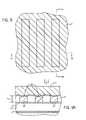
- FIG. 1illustrates a diagrammatic top plan view of a portion of a substrate at a preliminary processing stage according to an embodiment of the present disclosure, showing the substrate with a neutral wetting material thereon.
- FIGS. 1A-1Bare elevational, cross-sectional views of the substrate depicted in FIG. 1 taken along lines 1 A- 1 A and 1 B- 1 B, respectively.
- FIG. 2illustrates a diagrammatic top plan view of the substrate of FIG. 1 at a subsequent stage showing the formation of trenches in a material layer formed on the neutral wetting material.
- FIGS. 2A-2Billustrate elevational, cross-sectional views of a portion of the substrate depicted in FIG. 2 taken, respectively, along lines 2 A- 2 A and 2 B- 2 B.
- FIG. 3illustrates a side elevational view of a portion of a substrate at a preliminary processing stage according to another embodiment of the disclosure, showing the substrate with trenches in a material layer formed on the substrate.
- FIG. 4illustrates a side elevational view of the substrate of FIG. 3 at a subsequent stage showing the formation of a neutral wetting material within the trenches.
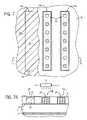
- FIG. 5is a diagrammatic top plan view of the substrate of FIG. 2 at a subsequent stage showing a block copolymer material within the trenches.
- FIGS. 5A-5Billustrate elevational, cross-sectional views of a portion of the substrate depicted in FIG. 5 taken along lines 5 A- 5 A and 5 B- 5 B, respectively.
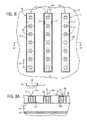
- FIGS. 6-8are diagrammatic top plan views of the substrate of FIG. 5 at subsequent stages showing annealing of a portion of the film according to an embodiment of the invention by a zoned annealing technique.
- FIGS. 6A-8Aillustrate elevational, cross-sectional views of the substrate depicted in FIGS. 6-8 taken along lines 6 A- 6 A, 7 A- 7 A and 8 A- 8 A, respectively, showing an embodiment of a heating device for zone annealing the film.
- FIG. 6Bis an elevational, cross-sectional view of the substrate depicted in FIG. 6 taken along lines 6 B- 6 B.
- FIG. 9is a top plan view of the substrate of FIG. 5 at a subsequent stage according to another embodiment of a method of the invention, illustrating placement of a non-preferential wetting material over the block copolymer material during an anneal.
- FIGS. 9A-9Bare elevational, cross-sectional views of the substrate depicted in FIG. 9 taken along lines 9 A- 9 A and 9 b- 9 B, respectively.
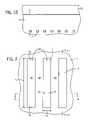
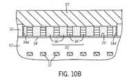
- FIGS. 10A-10Bare cross-sectional views of the substrate shown in FIGS. 9A-9B , respectively, at a subsequent stage showing the annealed, self-assembled block copolymer material, and removal of the non-preferential wetting material after the anneal.
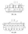
- FIGS. 11-13are top plan views of the substrate of FIG. 8 at subsequent stages, illustrating an embodiment of the use of the self-assembled block copolymer film after removal of one of the polymer blocks, as a mask to etch the substrate and filling of the etched openings.
- FIGS. 11A-13Aillustrate elevational, cross-sectional views of a portion of the substrate depicted in FIGS. 11-13 taken along lines 11 A- 11 A to 13 A- 13 A, respectively.
- FIGS. 11B-13Bare cross-sectional views of the substrate depicted in FIGS. 11-13 taken along lines 11 B- 11 B to 13 B- 13 B, respectively.
- semiconductor substrateor “semiconductive substrate” or “semiconductive wafer fragment” or “wafer fragment” or “wafer” will be understood to mean any construction comprising semiconductor material, including but not limited to bulk semiconductive materials such as a semiconductor wafer (either alone or in assemblies comprising other materials thereon), and semiconductive material layers (either alone or in assemblies comprising other materials).
- substraterefers to any supporting structure including, but not limited to, the semiconductive substrates, wafer fragments or wafers described above.
- L ois the inherent periodicity or pitch value (bulk period or repeat unit) of structures that self assemble upon annealing from a self-assembling (SA) block copolymer.
- L Bis the periodicity or pitch value of a blend of a block copolymer with one or more of its constituent homopolymers.
- Lis used herein to indicate the center-to-center cylinder pitch or spacing of cylinders of the block copolymer or blend, and is equivalent to “L o ” for a pure block copolymer and “L B ” for a copolymer blend.
- a polymer materiale.g., film, layer
- a polymer materialis prepared by guided self-assembly of block copolymers, with both polymer domains at the air interface.
- the block copolymer materialspontaneously assembles into periodic structures by microphase separation of the constituent polymer blocks after annealing, forming ordered domains of perpendicular-oriented cylinders at nanometer-scale dimensions within a trench.
- a method for fabricating a self-assembled block copolymer material that defines a one-dimensional (1-D) array of nanometer-scale, perpendicular-oriented cylinders according to an embodiment of the inventionis illustrated with reference to FIGS. 1-8 .
- the described embodimentinvolves a thermal anneal of a cylindrical-phase block copolymer under a solvent atmosphere.
- the annealis conducted in combination with a graphoepitaxy technique that utilizes a lithographically defined trench as a guide with a floor composed of a material that is neutral wetting to both polymer blocks, and sidewalls and ends that are preferential wetting to one polymer block and function as constraints to induce the block copolymer to self-assemble into an ordered 1-D array of a single row of cylinders in a polymer matrix oriented perpendicular to the trench floor and registered to the trench sidewalls.
- two or more rows of perpendicular-oriented cylinderscan be formed in each trench.
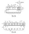
- a substrate 10is provided, which can be silicon, silicon oxide, silicon nitride, silicon oxynitride, silicon oxycarbide, among other materials.
- conductive lines 12or other active area, e.g., semiconducting regions are situated within the substrate 10 .
- a single trench or multiple trenchescan be formed in the substrate, and can span the entire width of an array of lines (or other active area).
- the substrate 10is provided with an array of conductive lines 12 (or other active areas) at a pitch of L.
- the trench or trenchesare formed over the active areas 12 (e.g., lines) such that when the block copolymer material is annealed, each cylinder will be situated above a single active area 12 (e.g., conductive line).
- multiple trenchesare formed with the ends ( 24 ) of each adjacent trench 18 aligned or slightly offset from each other at less than 5% of L such that cylinders in adjacent trenches are aligned and situated above the same line 12 .
- a neutral wetting material 14(e.g., random copolymer) has been formed over the substrate 10 .
- a material layer 16(or one or more material layers) can then be formed over the neutral wetting material and etched to form trenches 18 that are oriented perpendicular to the array of conductive lines 12 , as shown in FIGS. 2-2B . Portions of the material layer 16 form a spacer 20 outside and between the trenches.
- the trenches 18are structured with opposing sidewalls 22 , opposing ends 24 , a floor 26 , a width (w t ), a length (l t ) and a depth (D t ).
- the material layer 16 ′can be formed on the substrate 10 ′, etched to form the trenches 18 ′ as depicted in FIG. 3 , and a neutral wetting material 14 ′ can then be formed on the trench floors 26 ′ as shown in FIG. 4 .
- a random copolymer materialcan be deposited into the trenches 18 ′ and crosslinked to form a neutral wetting material layer. Material on surfaces outside the trenches such as on the spacers 20 ′ (e.g., non-crosslinked random copolymer) can be subsequently removed.
- Single or multiple trenches 18can be formed using a lithographic tool having an exposure system capable of patterning at the scale of L (10-100 nm).
- exposure systemsinclude, for example, extreme ultraviolet (EUV) lithography, proximity X-rays and electron beam (e-beam) lithography, as known and used in the art.
- EUVextreme ultraviolet
- e-beamelectron beam
- Conventional photolithographycan attain (at smallest) about 58 nm features.
- a method called “pitch doubling” or “pitch multiplication”can also be used for extending the capabilities of photolithographic techniques beyond their minimum pitch, as described, for example, in U.S. Pat. No. 5,328,810 (Lowrey et al.), U.S. Pat. No. 7,115,525 (Abatchev, et al.), US 2006/0281266 (Wells) and US 2007/0023805 (Wells).
- a pattern of linesis photolithographically formed in a photoresist material overlying a layer of an expendable material, which in turn overlies a substrate, the expendable material layer is etched to form placeholders or mandrels, the photoresist is stripped, spacers are formed on the sides of the mandrels, and the mandrels are then removed leaving behind the spacers as a mask for patterning the substrate.
- the initial photolithographyformed a pattern defining one feature and one space
- the same widthnow defines two features and two spaces, with the spaces defined by the spacers.
- the smallest feature size possible with a photolithographic techniqueis effectively decreased down to about 30 nm or less.
- Factors in forming a single (1-D) array or layer of perpendicular-oriented nanocylinders within the trenchesinclude the width (w t ) and depth (D t ) of the trench, the formulation of the block copolymer or blend to achieve the desired pitch (L), and the thickness (t) of the block copolymer material within the trench.
- a block copolymer or blend having a pitch or L value of 35-nm deposited into a 75-nm wide trench having a neutral wetting floorwill, upon annealing, result in a zigzag pattern of 17.5-nm diameter ( ⁇ 0.5*L) perpendicular cylinders that are offset by about one-half the pitch distance (about 0.5*L) for the length (l t ) of the trench, rather than a single line row of perpendicular cylinders aligned with the sidewalls down the center of the trench.
- the trenches 18are constructed with a width (w t ) of about 1.5 ⁇ 2*L (or 1.5 ⁇ 2 ⁇ the pitch value) of the block copolymer such that a cast block copolymer material (or blend) of about L will self assemble upon annealing into a single row of perpendicular cylinders (diameter ⁇ 0.5*L) with a center-to-center pitch distance (p) of adjacent cylinders at or about L.
- the width (w t ) of the trenches 18can be about 1.5 ⁇ 2*50 nm or about 75-100 nm.
- the length (l t ) of the trenchesis at or about n*L or an integer multiple of L, typically within a range of about n *10 to about n*100 nm (with n being the number of features or structures, e.g., cylinders).
- the depth (D t ) of the trenches 18is greater than or equal to L (D t >L).
- the width of the spacers 20 between adjacent trenchescan vary and is generally about L to about n*L.
- the trench dimensionis about 20-100 nm wide (w t ) and about 100-25,000 nm in length (l t ), with a depth (D t ) of about 10-100 nm.
- a self-assembling, cylindrical-phase block copolymer material 28 having an inherent pitch at or about L o (or a ternary blend of block copolymer and homopolymers blended to have a pitch at or about L B )is deposited into the trenches 18 , typically as a film (as in FIGS. 5-5B ).
- the block copolymer(or blend) is constructed such that all of the polymer blocks will have equal preference for a neutral wetting material on the trench floor.
- the block copolymer materialcan be constructed to provide desired properties such as defect tolerance and ease of development and/or removal of one of the blocks.
- the block copolymer or blendis constructed such that the minor domain can be selectively removed.
- diblock copolymersinclude, for example, poly(styrene)-b-poly(vinylpyridine) (PS-b-PVP), poly(styrene)-b-poly(methylmethacrylate) (PS-b-PMMA) or other PS-b-poly(acrylate) or PS-b-poly(methacrylate), poly(styrene)-b-poly(lactide) (PS-b-PLA), poly(styrene)-b-poly(tert-butyl acrylate) (PS-b-PtBA), and poly(styrene)-b-poly(ethylene-co-butylene (PS-b-(PS-co-PB)), poly(styrene)-b-poly(ethylene oxide) (PS-b-PEO), poly(isoprene)-b-poly(ethyleneoxide) (PI-b-PEO), poly(isoprene)-b-poly(methylme
- PS-b-PMMA block copolymer doped with PEO-coated gold nanoparticles of a size less than the diameter of the self-assembled cylindersPark et al, Macromolecules, 2007, 40(11), 8119-8124
- PS-b-P2VPpoly(styrene)-b-poly(2-vinylpyridine)
- PS-b-P2VPpoly(styrene)-b-poly(2-vinylpyridine) block copolymer having a cleavable junction such as a dithiol group, among others, with PS-b-PVP used in the illustrated embodiment.
- Other types of block copolymersi.e., triblock or multiblock copolymers can be used.
- triblock copolymersexamples include ABC copolymers such as poly(styrene-b-methyl methacrylate-b-ethylene oxide) (PS-b-PMMA-b-PEO), and ABA copolymers such as PS-PMMA-PS, PMMA-PS-PMMA, and PS-b-PI-b-PS, among others.
- ABC copolymerssuch as poly(styrene-b-methyl methacrylate-b-ethylene oxide) (PS-b-PMMA-b-PEO)
- ABA copolymerssuch as PS-PMMA-PS, PMMA-PS-PMMA, and PS-b-PI-b-PS, among others.
- the film morphologyincluding the domain sizes and periods (L o ) of the microphase-separated domains, can be controlled by chain length of a block copolymer (molecular weight, MW) and volume fraction of the AB blocks of a diblock copolymer to produce cylindrical morphologies (among others).
- a block copolymermolecular weight, MW
- volume fraction of the AB blocks of a diblock copolymerto produce cylindrical morphologies (among others).
- the diblock copolymerwill microphase separate and self-assemble into periodic cylindrical domains of polymer B within a matrix of polymer A.
- An example of a cylinder-forming PS-b-PVP copolymer material (L o ⁇ 28 nm) to form about 14 nm diameter cylindrical PVP domains in a matrix of PSis composed of about 70 wt-% PS and 30 wt-% PVP with a total molecular weight (M n ) of 44.5 kg/mol.
- the L value of the block copolymercan be modified, for example, by adjusting the molecular weight of the block copolymer.
- the block copolymer materialcan also be formulated as a binary or ternary blend comprising a block copolymer and one or more homopolymers (HPs) of the same type of polymers as the polymer blocks in the block copolymer, to produce a blend that will swell the size of the polymer domains and increase the L value.
- the concentration of homopolymers in the blendcan range from 0 to about 60 wt-%.
- a ternary diblock copolymer blendis a PS-b-P2VP/PS/P2VP blend, for example, 60 wt-% of 32.5 K/12 K PS-b-P2VP, 20 wt-% of 10 K PS, and 20 wt-% of 10 K P2VP.
- Another example of a ternary diblock copolymer blendis a PS-b-PMMA/PS/PMMA blend, for example, 60 wt-% of 46K/21K PS-b-PMMA, 20 wt-% of 20K polystyrene and 20 wt-% of 20K poly(methyl methacrylate).
- Yet another exampleis a blend of 60:20:20 (wt-%) of PS-b-PEO/PS/PEO, or a blend of about 85-90 wt-% PS-b-PEO and up to 10-15 wt-% PEO; it is believed that the added PEO homopolymer may function, at least in part, to lower the surface energy of the PEO domains to that of PS.
- the trench floors 26are structured to be neutral wetting (equal affinity for both blocks of the copolymer) to induce formation of cylindrical polymer domains that are oriented perpendicular to the trench floors, and the trench sidewalls 22 and ends 24 are structured to be preferential wetting by one block of the block copolymer to induce registration of the cylinders to the sidewalls as the polymer blocks self-assemble.
- the preferred or minority block of the cylindrical-phase block copolymerwill self-assemble to form a single row of cylindrical domains in the center of a polymer matrix for the length of the trench and segregate to the sidewalls and edges of the trench to form a thin interface brush or wetting layer (e.g., as in FIGS. 6-6B ).
- Entropic forcesdrive the wetting of a neutral wetting surface by both blocks, and enthalpic forces drive the wetting of a preferential-wetting surface by the preferred block (e.g., the minority block).
- the material layer 16can be composed of silicon (with native oxide), oxide (e.g., silicon oxide, SiO x ), silicon nitride, silicon oxycarbide, indium tin oxide (ITO), silicon oxynitride, and resist materials such as methacrylate-based resists and polydimethyl glutarimide resists, among other materials, which exhibit preferential wetting toward the PVP (or PMMA, etc.) block.
- oxidee.g., silicon oxide, SiO x
- silicon nitridesilicon oxycarbide
- ITOindium tin oxide
- resist materialssuch as methacrylate-based resists and polydimethyl glutarimide resists, among other materials, which exhibit preferential wetting toward the PVP (or PMMA, etc.) block.
- the block copolymer materialwill self assemble to form a thin interface layer and cylinders of PVP in a PS matrix.
- a preferential wetting materialsuch as a polymethylmethacrylate (PMMA) polymer modified with an —OH containing moiety (e.g., hydroxyethylmethacrylate) can be applied onto the surfaces of the trenches, for example, by spin coating and then heating (e.g., to about 170° C.) to allow the terminal OH groups to end-graft to oxide sidewalls 22 and ends 24 of the trenches.
- Non-grafted materialcan be removed by rinsing with an appropriate solvent (e.g., toluene). See, for example, Mansky et al., Science, 1997, 275, 1458-1460, and In et al., Langmuir, 2006, 22, 7855-7860.
- a neutral wetting trench floor 26allows both blocks of the copolymer material to wet the floor of the trench.
- a neutral wetting material 14can be provided by applying a neutral wetting polymer (e.g., a neutral wetting random copolymer) onto the substrate 10 , forming the material layer 16 and then etching the trenches to expose the underlying neutral wetting material, as illustrated in FIGS. 2-2B .
- a neutral wetting polymere.g., a neutral wetting random copolymer
- a neutral wetting random copolymer materialcan be applied after forming the trenches 18 ′, for example, as a blanket coat by casting or spin-coating into the trenches, as depicted in FIG. 4 .
- the random copolymer materialcan then be thermally processed to flow the material into the bottom of the trenches by capillary action, which results in a layer (mat) 14 ′ composed of the crosslinked, neutral wetting random copolymer.
- the random copolymer material within the trenchescan be photo-exposed (e.g., through a mask or reticle) to crosslink the random copolymer within the trenches to form the neutral wetting material 14 ′.
- Non-crosslinked random copolymer material outside the trenchese.g., on the spacers 20 ′
- Neutral wetting surfacescan be specifically prepared by the application of random copolymers composed of monomers identical to those in the block copolymer and tailored such that the mole fraction of each monomer is appropriate to form a neutral wetting surface.
- a neutral wetting material 14can be formed from a thin film of a photo-crosslinkable random PS-r-PVP that exhibits non-preferential or neutral wetting toward PS and PVP, which can be cast onto the substrate 10 (e.g., by spin coating).
- the random copolymer materialcan be fixed in place by chemical grafting (on an oxide substrate) or by thermally or photolytically crosslinking (any surface) to form a mat that is neutral wetting to PS and PVP and insoluble when the block copolymer material is cast onto it, due to the crosslinking.
- a photo-crosslinkable PS-r-PMMA random copolymere.g., containing an about 0.6 mole fraction of styrene
- another neutral wetting surface for PS-b-PMMAcan be provided by hydrogen-terminated silicon.
- the floors 26 of the trenches 18can be etched, for example, with a hydrogen plasma, to remove the oxide material and form hydrogen-terminated silicon, which is neutral wetting with equal affinity for both blocks of a block copolymer material.
- H-terminated siliconcan be prepared by a conventional process, for example, by a fluoride ion etch of a silicon substrate (with native oxide present, about 12-15 ⁇ ) by exposure to an aqueous solution of hydrogen fluoride (HF) and buffered HF or ammonium fluoride (NH 4 F), by HF vapor treatment, or by a hydrogen plasma treatment (e.g., atomic hydrogen).
- a fluoride ion etch of a silicon substratewith native oxide present, about 12-15 ⁇
- HFhydrogen fluoride
- NH 4 Fbuffered HF or ammonium fluoride
- HF vapor treatmente.g., atomic hydrogen
- An H-terminated silicon substratecan be further processed by grafting a random copolymer such as PS-r-PVP, PS-r-PMMA, etc. selectively onto the substrate resulting in a neutral wetting surface for the corresponding block copolymer (e.g, PS-b-PVP, PS-b-PMMA, etc.).
- a neutral wetting layer of a PS-r-PMMA random copolymercan be provided by an in situ free radical polymerization of styrene and methyl methacrylate using a di-olefinic linker such as divinyl benzene which links the polymer to the surface to produce about a 10-15 nm thick film.
- a neutral wetting random copolymer material 14 ′can be applied after formation of the material layer 16 ′ and trenches 18 ′, which reacts selectively with the trench floor 26 ′ (composed of the substrate 10 ′ material) and not the trench sidewalls 22 ′ or ends 24 ′ (composed of the material layer 16 ′).
- a random copolymer (or appropriate blend of homopolymers with block copolymer surfactant) containing epoxide groupswill react selectively to terminal amine functional groups (e.g. —NH— and —NH 2 ) on silicon nitride and silicon oxynitride surfaces relative to silicon oxide or silicon.
- the trench floor 26 ′is silicon or polysilicon and the sidewalls 22 ′ are a material such as an oxide (e.g., SiO x ), the floor can be treated to form H-terminated silicon and a random copolymer material 14 ′ (e.g., PS-r-PVP, PS-r-PMMA, etc.) can be formed in situ only at the floor surface.
- a random copolymer material 14 ′e.g., PS-r-PVP, PS-r-PMMA, etc.
- a neutral wetting surface(e.g., for PS-b-PMMA and PS-b-PEO) can be provided by grafting a self-assembled monolayer (SAM) of a trichlorosilane-base SAM such as 3-(para-methoxyphenyl)propyltrichorosilane grafted to oxide (e.g., SiO 2 ) as described for example, by D. H. Park, Nanotechnology 18 (2007), p. 355304.
- SAMself-assembled monolayer
- oxidee.g., SiO 2
- a neutral wetting random copolymer of polystyrene (PS), polymethacrylate (PMMA) with hydroxyl group(s)e.g., 2-hydroxyethyl methacrylate (P(S-r-MMA-r-HEMA)
- PMMApolymethacrylate
- P(S-r-MMA-r-HEMA)2-hydroxyethyl methacrylate
- a substrate 10e.g., an oxide
- a neutral wetting layer 14about 5-10 nm thick by heating at about 160° C. for about 48 hours. See, for example, In et al., Langmuir, 2006, 22, 7855-7860.
- a blend of hydroxyl-terminated homopolymers and a corresponding low molecular weight block copolymercan be grafted (covalently bonded) to the substrate to form a neutral wetting interface layer (e.g., about 4-5 nm) for PS-b-PMMA and PS-b-P2VP, among other block copolymers.
- the block copolymercan function to emulsify the homopolymer blend before grafting.
- an about 1 wt-% solutione.g., in toluene
- about 80-50 wt-% (or about 70-60 wt-%) of a low molecular weight block copolymere.g., 5K-5K
- a substrate 10e.g., SiO 2
- heated (baked)e.g., at 160° C.
- non-grafted (unbonded) polymer materialremoved, for example by a solvent rinse (e.g., toluene).
- a surface that is neutral wetting to PS-b-PMMAcan also be prepared by spin coating a blanket layer of a photo- or thermally cross-linkable random copolymer such as a benzocyclobutene- or azidomethylstyrene-functionalized random copolymer of styrene and methyl methacrylate (e.g., poly(styrene-r-benzocyclobutene-r-methyl methacrylate (PS-r-PMMA-r-BCB)).
- a photo- or thermally cross-linkable random copolymersuch as a benzocyclobutene- or azidomethylstyrene-functionalized random copolymer of styrene and methyl methacrylate (e.g., poly(styrene-r-benzocyclobutene-r-methyl methacrylate (PS-r-PMMA-r-BCB)).
- such a random copolymercan comprise about 42 wt-% PMMA, about (58-x) wt-% PS and x wt-% (e.g., about 2-3 wt-%) of either polybenzocyclobutene or poly(para-azidomethylstyrene)).
- An azidomethylstyrene-functionalized random copolymercan be UV photo-crosslinked (e.g., 1-5 MW/cm ⁇ 2 exposure for about 15 seconds to about 30 minutes) or thermally crosslinked (e.g., at about 170° C. for about 4 hours) to form a crosslinked polymer mat as a neutral wetting layer 14 .
- a benzocyclobutene-functionalized random copolymercan be thermally cross-linked (e.g., at about 200° C. for about 4 hours or at about 250° C. for about 10 minutes).
- a self-assembling, cylindrical-phase block copolymer material 28 having an inherent pitch at or about L o(or a ternary blend of block copolymer and homopolymers blended to have a pitch at or about L B ) can be cast or deposited into the trenches 18 to a thickness (t 1 ) at or about the L value of the block copolymer material (e.g., about ⁇ 20% of L) such that after annealing (e.g., FIGS.
- the thickness (t 2 )will be at or about the L value and the block copolymer material will self assemble to form a single layer of cylinders having a diameter of about 0.5*L (e.g., 5-50 nm, or about 20 nm, for example) within a polymer matrix in a single row within each trench 18 .
- the thickness of the block copolymer material 28can be measured, for example, by ellipsometry techniques.
- the block copolymer materialcan be deposited by spin casting (spin-coating) from a dilute solution (e.g., about 0.25-2 wt % solution) of the copolymer in an organic solvent such as dichloroethane (CH 2 Cl 2 ) or toluene, for example. Capillary forces pull excess block copolymer material 28 (e.g., greater than a monolayer) into the trenches 18 . As shown, a thin layer or film 28 a of the block copolymer material can be deposited onto the material layer 16 outside the trenches, e.g., on the spacers 20 . Upon annealing, the thin film 28 a will flow into the trenches leaving a structureless brush layer on the material layer 16 from a top-down perspective.
- a dilute solutione.g., about 0.25-2 wt % solution
- organic solventsuch as dichloroethane (CH 2 Cl 2 ) or toluene
- the block copolymer (BCP) material 28is then heated above its glass transition temperature under a vapor phase containing a partly-saturated concentration of an organic solvent to cause the polymer blocks to phase separate and self assemble according to the preferential and neutral wetting of the trench surfaces to form a self-assembled polymer material 30 , as illustrated in FIGS. 6-6B .
- the appropriate partial pressure of solvent vapor to achieve a neutral wetting vapor interface at a particular temperaturedepends, at least in part, on the block copolymer that is used and can be determined empirically.
- the block copolymeris heated at a thermal anneal temperature that is above its glass transition temperature (T g ) but below the decomposition or degradation temperature (T d ) of the block copolymer material.
- a PS-b-PVP block copolymer materialcan be annealed at a temperature of about 150-275° C. in a solvent vapor atmosphere for about 1-24 hours to achieve a self-assembled morphology.
- a PS-b-PMMA block copolymer materialcan be annealed at a temperature of about 150-275° C. in a solvent vapor atmosphere for about 1-24 hours to achieve a self-assembled morphology.
- the air interfaceis preferentially wetting to one of the polymer domains and the BCP material does not orient into perpendicular structures.
- the BCP material 28is exposed to solvent vapors of a “good” solvent for both blocks, that is, a neutral organic solvent that solvates both the constituent blocks well.
- solvent annealingconsists of two phases.
- a first phasethe BCP material is exposed to a solvent vapor that acts to plasticize the film and increase chain mobility causing the domains to intermingle and the loss of order inherent from casting the polymer material.
- the organic solvent that is utilizedis based at least in part on its solubility in the block copolymer material such that sufficient solvent molecules enter the block copolymer material to promote the order-disorder transition of the polymer domains and enable the required molecular rearrangement.
- solventsexamples include aromatic solvents such as benzene, toluene, xylene, dimethoxyethane, ethyl acetate, cyclohexanone, etc., and chlorinated solvents such as chloroform, methylene chloride, a chloroform/octane mixture, etc., among others.
- aromatic solventssuch as benzene, toluene, xylene, dimethoxyethane, ethyl acetate, cyclohexanone, etc.
- chlorinated solventssuch as chloroform, methylene chloride, a chloroform/octane mixture, etc., among others.
- the evaporation of the solventis highly directional and forms a solvent gradient from the “top” (surface) of the BCP material to the “bottom” of the BCP material at the trench floor that induces orientation and self-assembly of structures starting at the air-surface interface, which is neutral wetting due to the partial pressure of solvent at the interface, and driven downward to the floor of the trench, with formation of perpendicular-oriented cylindrical domains ( 34 ) guided by the trench sidewalls and extending completely from the air interface ( 46 ) to the substrate surface (trench floor).
- the substrate 10 and BCP material 28are heated above the boiling point of the solvent such that swelling of the BCP material by the solvent is disallowed.
- the use of a partly-saturated solvent vapor phase above the block copolymer materialprovides a neutral wetting interface, similar to the second phase of solvent annealing.
- the concentration of solvent in the air immediate at the vapor interface with the BCP materialis maintained at or under saturation to maintain a neutral wetting interface such that both (or all) polymer blocks will equally wet the vapor interface.
- both the air and trench floorare neutral wetting, the domains will orient perpendicular throughout the film layer, with the preferential wetting sidewalls inducing lateral order.
- the resulting morphology of the annealed copolymer material 30can be examined, for example, using atomic force microscopy (AFM), transmission electron microscopy (TEM), scanning electron microscopy (SEM), among others.
- AFMatomic force microscopy
- TEMtransmission electron microscopy
- SEMscanning electron microscopy
- the annealis performed by globally heating the block copolymer within the trenches in a solvent atmosphere.
- a zone annealingis conducted to anneal portions or sections of the block copolymer material 28 in trenches on the substrate 10 by a localized application of thermal energy (e.g., heat). Zone annealing can provide rapid self-assembly of the block copolymer material (e.g., on the order of minutes).
- thermal energye.g., heat
- the substrate 10in a vapor atmosphere
- a thermal or heat source 32(or combined heating and cooling source) can be moved relative to each other (e.g., arrow ⁇ ) such that heat is applied above (or underneath) the substrate 10 .
- Only a portion of the BCP materialis initially heated above the glass transition temperature and the heated zone is then “pulled” across the substrate (or vice versa).
- a thermal source 32can be moved across the substrate 10 at a translational set speed (e.g., about 0.05-10 ⁇ m/second using a mechanism such as a motorized translation stage (not shown). Pulling the heated zone across the substrate (or vice versa) can result in faster processing and better ordered structures relative to a global thermal anneal.
- a hot-to-cold temperature gradientcan be provided over (or under) the substrate such that a certain portion of the substrate is heated and then cooled, which can be at a controlled rate.
- the substratecan be exposed to a cold-to-hot temperature gradient to anneal the BCP material, followed by cooling.
- the BCP materialcan be heated above and then cooled below the order-disorder temperature (but above the glass transition temperature), for example, to remove (melt out) defects and allow the material to recrystalize provided that the order-disorder temperature (T o-d ) is less than the decomposition temperature (T d ) of the block copolymer material.
- the order-disorder temperatureis defined by the temperature dependence of the block copolymer, Chi value, the total number of monomers per chain, and the monomer composition.
- the block copolymer material within trench 18 acan be heated and annealed to form a self-assembled material 30 while the unannealed block copolymer material 28 within trenches 18 b , 18 c remains disordered. Only those portions of the block copolymer material 28 that are heated above the glass transition temperature (T g ) will self-assemble.
- a next portion of the substratecan then be selectively heated, as shown in FIGS. 7-7A , resulting in the self assembly of the block copolymer material within trench 18 b .
- a subsequent heating of the remaining areas of the substratecan then be conducted, e.g., as depicted in FIGS. 8-8A .
- the cylindrical-phase block copolymer material 28Upon annealing, the cylindrical-phase block copolymer material 28 will self-assemble into a polymer material 30 (e.g. film) in response to the character of the block copolymer composition (e.g., PS-b-PVP having an inherent pitch at or about L) and the boundary conditions, including the constraints provided by the width (w t ) of the trench 18 and the wetting properties of the trench surfaces including a trench floor 26 that exhibits neutral or non-preferential wetting toward both polymer blocks (e.g., a random graft copolymer), sidewalls 22 that are preferential wetting by the minority (preferred) block of the block copolymer (e.g., the PVP block), and the presence of a neutral or non-preferential solvent (or in some embodiments, a film or material that is neutral or non-preferential wetting) in contact with the surface of the block copolymer material 26 in the trenches.
- the annealresults in a row (or rows) of perpendicularly-oriented cylinders 34 of the minority polymer (preferred) block (e.g., PVP) within a matrix 36 of the majority polymer block (e.g., PS), with the cylinders registered and parallel to the sidewalls 22 of the trench.
- the diameter of the cylinders 34will generally be at or about 0.5*L (e.g., about one-half of the center-to-center distance between cylinders).
- the minority (preferred) blocke.g., PVP
- PVPminority (preferred) block
- the minority (preferred) blockwill segregate to and wet the preferential wetting sidewalls 22 and ends 24 of the trenches 18 to form a thin interface or wetting brush layer 34 a having a thickness generally about one-fourth of the center-to-center distance between adjacent cylinders 34 .
- a layer of the PVP blockwill wet oxide interfaces with attached PS domains directed outward from the oxide material.
- the self-assembled block copolymer material 30is defined by a single layer of an array of cylindrical domains (cylinders) 34 , each with a diameter at or about 0.5* L (e.g., about one-half of the center-to-center distance between cylinders), with the number (n) of cylinders in the row according to the length (l t ) of the trench, and the center-to-center distance (pitch distance, p) between each cylinder at or about L.
- Le.g., about one-half of the center-to-center distance between cylinders
- the copolymer materialcan be treated to crosslink the polymer segments (e.g., the PS segments) to fix and enhance the strength of the self-assembled polymer blocks.
- the polymerscan be structured to inherently crosslink (e.g., upon exposure to ultraviolet (UV) radiation, including deep ultraviolet (DUV) radiation), or one of the polymer blocks of the copolymer material can be formulated to contain a crosslinking agent.
- the film 28 a outside the trenches(e.g., on spacers 18 ) will not be thick enough to result in self-assembly.
- the unstructured thin film 28 acan be removed, as illustrated in FIGS. 8-8A , for example, by an etch technique or a planarization process to provide an about uniformly flat surface.
- the trench regionscan be selectively exposed through a reticle (not shown) to crosslink only the annealed and self-assembled polymer material 30 within the trenches 18 , and a wash can then be applied with an appropriate solvent (e.g., toluene) to remove the non-crosslinked portions of the block copolymer material 28 a (e.g., on the spacers 20 ), leaving the registered self-assembled polymer material within the trench and exposing the surface of the material layer 16 above/outside the trenches.
- an appropriate solvente.g., toluene
- the annealed polymer material 30can be crosslinked globally, a photoresist material can be applied to pattern and expose the areas of the polymer material 28 a outside the trench regions, and the exposed portions of the polymer material 28 a can be removed, for example by an oxygen (O 2 ) plasma treatment.
- O 2oxygen
- a thermal annealis conducted while applying a non-preferentially wetting material 37 ′ to the surface of the block copolymer (BCP) material 28 ′ in the trenches.
- the non-preferential wetting material 37 ′is composed of a solid material, which can be physically placed onto the BCP material 28 ′, for example, a soft, flexible or rubbery solid material such as a cross-linked, poly(dimethylsiloxane) (PDMS) elastomer (e.g., Sylgard-184 by Dow-Corning) or other elastomeric polymer material (e.g., silicones, polyurethanes, etc.), which provides an external surface that is neutral wetting.
- PDMSpoly(dimethylsiloxane)
- the solid materialcan be derivatized (e.g., by grafting a random copolymer) such that it presents a neutral wetting surface.
- a thermal annealing processis conducted (arrows ⁇ , FIGS. 9A-9B ) to cause the polymer blocks to phase separate in response to the preferential and neutral wetting of the trench surfaces and the non-preferential (neutral) wetting of the overlying material 37 ′, and form a self-assembled polymer material 30 ′ as illustrated in FIGS. 10A-10B .
- the non-preferential wetting material 37 ′can be removed from contact with the annealed polymer material 30 ′ (arrow ⁇ ) as depicted in FIG. 10A .
- a PDMS or other elastomeric material layer 37 ′can be removed, for example, by lifting or peeling the material from the surface of the annealed polymer material.
- a solventsuch as water, alcohols, and the like, which is compatible with and does not dissolve the block copolymer material 30 ′, can be applied (e.g., by soaking) to permeate and swell the elastomeric material (e.g., PDMS) to enhance physical removal.
- a dilute fluoride solutione.g., NH 4 F, HF, NaF, etc.
- the pattern of perpendicular-oriented cylinders that is formed on the substratecan then be further processed as desired, for example, to form an etch mask for patterning nanosized features into the underlying substrate 10 through selective removal of one block of the self-assembled block copolymer.
- MWchain length of a block copolymer
- resolutioncan exceed other techniques such as conventional photolithography. Processing costs using the technique is significantly less than extreme ultraviolet (EUV) photolithography, which has comparable resolution.
- EUVextreme ultraviolet
- an etch mask 38can be formed by selectively removing the cylindrical polymer domains 34 of the self-assembled polymer material 30 to produce openings 40 in the polymer matrix 36 (e.g., PS) to expose the underlying substrate 10 at the trench floors 26 .
- the cylindrical domains 34can be removed by a selective wet etch (e.g., PMMA and PLA by UV exposure/acetic acid development, PLA by aqueous methanol mixture containing sodium hydroxide, PEO by aqueous hydroiodic acid or water, etc.) or by a selective reactive ion etch (RIE) process.
- a selective wet etche.g., PMMA and PLA by UV exposure/acetic acid development, PLA by aqueous methanol mixture containing sodium hydroxide, PEO by aqueous hydroiodic acid or water, etc.
- RIEselective reactive ion etch
- the filmcan be exposed to a solvent selective to the minor domain, for example, an alcohol for PVP, water for PEO or PLA, and acetic acid for PMMA, that contains a cleaving agent to remove (e.g., wash out) the minor domain.
- a solvent selective to the minor domainfor example, an alcohol for PVP, water for PEO or PLA, and acetic acid for PMMA, that contains a cleaving agent to remove (e.g., wash out) the minor domain.
- the remaining porous polymere.g.
- PS matrix 36can then be used as a lithographic template or mask to etch (arrows ⁇ ) a series of cylindrical-shaped openings or contact holes 42 in the nanometer size range (e.g., about 10-100 nm) to the conductive lines 12 or other active area (e.g., semiconducting region, etc.) in the underlying substrate 10 (or an underlayer).
- the openings 42can be formed, for example, using a selective reactive ion etching (RIE) process.
- the residual polymer matrix 36can be removed (e.g., PS by an oxidation process such as a plasma O 2 etch) and the substrate openings 42 can be filled with a material 44 such as a metal or metal alloy such as Cu, Al, W, Si, and Ti 3 N 4 , among others, to form arrays of cylindrical contacts to the conductive lines 12 .
- the cylindrical openings 42 in the substratecan also be filled with a metal-insulator-metal stack to form capacitors with an insulating material such as SiO 2 , Al 2 O 3 , HfO 2 , ZrO 2 , SrTiO 3 , and the like.
- Embodiments of the inventionutilize a thermal anneal process in combination with solvent annealing, which can provide faster processing than with a solvent anneal alone and expands the types of block copolymers (BCPs) that can be processed to substantially all BCPs.
- BCPsblock copolymers
- a wide range of block copolymerscan be processed to form perpendicular-oriented nanostructures (e.g., cylinders) and at a rapid rate.
- methods of the disclosureprovide a means of generating self-assembled diblock copolymer films composed of perpendicular-oriented cylinders in a polymer matrix.
- the methodsprovide ordered and registered elements on a nanometer scale that can be prepared more inexpensively than by electron beam lithography, EUV photolithography or conventional photolithography.
- the feature sizes produced and accessible by this inventioncannot be easily prepared by conventional photolithography.
- the described methods and systemscan be readily employed and incorporated into existing semiconductor manufacturing process flows and provide a low cost, high-throughput technique for fabricating small structures.
Landscapes
- Engineering & Computer Science (AREA)
- Chemical & Material Sciences (AREA)
- Manufacturing & Machinery (AREA)
- Physics & Mathematics (AREA)
- General Physics & Mathematics (AREA)
- Microelectronics & Electronic Packaging (AREA)
- Condensed Matter Physics & Semiconductors (AREA)
- Computer Hardware Design (AREA)
- Power Engineering (AREA)
- Nanotechnology (AREA)
- Inorganic Chemistry (AREA)
- Chemical Kinetics & Catalysis (AREA)
- Polymers & Plastics (AREA)
- Medicinal Chemistry (AREA)
- Organic Chemistry (AREA)
- Health & Medical Sciences (AREA)
- Analytical Chemistry (AREA)
- Composite Materials (AREA)
- Crystallography & Structural Chemistry (AREA)
- Materials Engineering (AREA)
- General Chemical & Material Sciences (AREA)
- Optics & Photonics (AREA)
- Exposure Of Semiconductors, Excluding Electron Or Ion Beam Exposure (AREA)
- Treatments Of Macromolecular Shaped Articles (AREA)
- Manufacture Of Macromolecular Shaped Articles (AREA)
- Formation Of Insulating Films (AREA)
- Application Of Or Painting With Fluid Materials (AREA)
Abstract
Description
- Embodiments of the invention relate to methods of fabricating thin films of self-assembling block copolymers, and devices resulting from those methods.
- As the development of nanoscale mechanical, electrical, chemical and biological devices and systems increases, new processes and materials are needed to fabricate nanoscale devices and components. Making electrical contacts to conductive lines has become a significant challenge as the dimensions of semiconductor features shrink to sizes that are not easily accessible by conventional lithography. Optical lithographic processing methods have difficulty fabricating structures and features at the sub-60 nanometer level. The use of self assembling diblock copolymers presents another route to patterning at nanoscale dimensions. Diblock copolymer films spontaneously assembly into periodic structures by microphase separation of the constituent polymer blocks after annealing, for example by thermal annealing above the glass transition temperature of the polymer or by solvent annealing, forming ordered domains at nanometer-scale dimensions.
- The film morphology, including the size and shape of the microphase-separated domains, can be controlled by the molecular weight and volume fraction of the AB blocks of a diblock copolymer to produce lamellar, cylindrical, or spherical morphologies, among others. For example, for volume fractions at ratios greater than about 80:20 of the two blocks (AB) of a diblock polymer, a block copolymer film will microphase separate and self-assemble into a periodic spherical domains with spheres of polymer B surrounded by a matrix of polymer A. For ratios of the two blocks between about 60:40 and 80:20, the diblock copolymer assembles into a periodic hexagonal close-packed or honeycomb array of cylinders of polymer B within a matrix of polymer A. For ratios between about 50:50 and 60:40, lamellar domains or alternating stripes of the blocks are formed. Domain size typically ranges from 5-50 nm.
- Many applications of the self-assembly of block copolymers (BCPs) to lithography require that the self-assembled domains orient perpendicular to the substrate with both domains wetting and exposed at the air interface. With selective removal of one of the polymer blocks to form an etch mask, the perpendicularly-oriented void structures can then be used for etching the underlying substrate.
- Conventional thermal annealing of most BCPs (e.g., PS-b-PVP, etc.) in air or vacuum will typically result in one block preferentially wetting the air vapor interface. A variant of thermal annealing called zone annealing, can provide rapid self-assembly (e.g., on the order of minutes) but is only effective for a small number of BCPs (e.g., PS-b-PMMA, PS-b-PLA) with polymer domains that equally wet the air vapor interface. Solvent annealing of BCPs has been used to produce a perpendicular orientation of the self-assembled domains to the substrate, but is generally a very slow process, typically on the order of days, and can require large volumes of the solvent. A typical solvent anneal is conducted by exposing a BCP film to a saturated solvent atmosphere at 25° C. for at least 12 hours (often longer).
- It would be useful to provide methods of fabricating films of arrays of ordered nanostructures that overcome these problems.
- Embodiments of the invention are described below with reference to the following accompanying drawings, which are for illustrative purposes only. Throughout the following views, the reference numerals will be used in the drawings, and the same reference numerals will be used throughout the several views and in the description to indicate same or like parts.
FIG. 1 illustrates a diagrammatic top plan view of a portion of a substrate at a preliminary processing stage according to an embodiment of the present disclosure, showing the substrate with a neutral wetting material thereon.FIGS. 1A-1B are elevational, cross-sectional views of the substrate depicted inFIG. 1 taken alonglines 1A-1A and1B-1B, respectively.FIG. 2 illustrates a diagrammatic top plan view of the substrate ofFIG. 1 at a subsequent stage showing the formation of trenches in a material layer formed on the neutral wetting material.FIGS. 2A-2B illustrate elevational, cross-sectional views of a portion of the substrate depicted inFIG. 2 taken, respectively, alonglines 2A-2A and2B-2B.FIG. 3 illustrates a side elevational view of a portion of a substrate at a preliminary processing stage according to another embodiment of the disclosure, showing the substrate with trenches in a material layer formed on the substrate.FIG. 4 illustrates a side elevational view of the substrate ofFIG. 3 at a subsequent stage showing the formation of a neutral wetting material within the trenches.FIG. 5 is a diagrammatic top plan view of the substrate ofFIG. 2 at a subsequent stage showing a block copolymer material within the trenches.FIGS. 5A-5B illustrate elevational, cross-sectional views of a portion of the substrate depicted inFIG. 5 taken along lines5A-5A and5B-5B, respectively.FIGS. 6-8 are diagrammatic top plan views of the substrate ofFIG. 5 at subsequent stages showing annealing of a portion of the film according to an embodiment of the invention by a zoned annealing technique.FIGS. 6A-8A illustrate elevational, cross-sectional views of the substrate depicted inFIGS. 6-8 taken alonglines 6A-6A,7A-7A and8A-8A, respectively, showing an embodiment of a heating device for zone annealing the film.FIG. 6B is an elevational, cross-sectional view of the substrate depicted inFIG. 6 taken alonglines 6B-6B.FIG. 9 is a top plan view of the substrate ofFIG. 5 at a subsequent stage according to another embodiment of a method of the invention, illustrating placement of a non-preferential wetting material over the block copolymer material during an anneal.FIGS. 9A-9B are elevational, cross-sectional views of the substrate depicted inFIG. 9 taken alonglines 9A-9A and9b-9B, respectively.FIGS. 10A-10B are cross-sectional views of the substrate shown inFIGS. 9A-9B , respectively, at a subsequent stage showing the annealed, self-assembled block copolymer material, and removal of the non-preferential wetting material after the anneal.FIGS. 11-13 are top plan views of the substrate ofFIG. 8 at subsequent stages, illustrating an embodiment of the use of the self-assembled block copolymer film after removal of one of the polymer blocks, as a mask to etch the substrate and filling of the etched openings.FIGS. 11A-13A illustrate elevational, cross-sectional views of a portion of the substrate depicted inFIGS. 11-13 taken alonglines 11A-11A to13A-13A, respectively.FIGS. 11B-13B are cross-sectional views of the substrate depicted inFIGS. 11-13 taken alonglines 11B-11B to13B-13B, respectively.- The following description with reference to the drawings provides illustrative examples of devices and methods according to embodiments of the invention. Such description is for illustrative purposes only and not for purposes of limiting the same.
- In the context of the current application, the term “semiconductor substrate” or “semiconductive substrate” or “semiconductive wafer fragment” or “wafer fragment” or “wafer” will be understood to mean any construction comprising semiconductor material, including but not limited to bulk semiconductive materials such as a semiconductor wafer (either alone or in assemblies comprising other materials thereon), and semiconductive material layers (either alone or in assemblies comprising other materials). The term “substrate” refers to any supporting structure including, but not limited to, the semiconductive substrates, wafer fragments or wafers described above.
- “Lo” as used herein is the inherent periodicity or pitch value (bulk period or repeat unit) of structures that self assemble upon annealing from a self-assembling (SA) block copolymer. “LB” as used herein is the periodicity or pitch value of a blend of a block copolymer with one or more of its constituent homopolymers. “L” is used herein to indicate the center-to-center cylinder pitch or spacing of cylinders of the block copolymer or blend, and is equivalent to “Lo” for a pure block copolymer and “LB” for a copolymer blend.
- In embodiments of the invention, a polymer material (e.g., film, layer) is prepared by guided self-assembly of block copolymers, with both polymer domains at the air interface. The block copolymer material spontaneously assembles into periodic structures by microphase separation of the constituent polymer blocks after annealing, forming ordered domains of perpendicular-oriented cylinders at nanometer-scale dimensions within a trench.
- A method for fabricating a self-assembled block copolymer material that defines a one-dimensional (1-D) array of nanometer-scale, perpendicular-oriented cylinders according to an embodiment of the invention is illustrated with reference to
FIGS. 1-8 . - The described embodiment involves a thermal anneal of a cylindrical-phase block copolymer under a solvent atmosphere. The anneal is conducted in combination with a graphoepitaxy technique that utilizes a lithographically defined trench as a guide with a floor composed of a material that is neutral wetting to both polymer blocks, and sidewalls and ends that are preferential wetting to one polymer block and function as constraints to induce the block copolymer to self-assemble into an ordered 1-D array of a single row of cylinders in a polymer matrix oriented perpendicular to the trench floor and registered to the trench sidewalls. In some embodiments, two or more rows of perpendicular-oriented cylinders can be formed in each trench.
- As depicted in
FIGS. 1-1B , asubstrate 10 is provided, which can be silicon, silicon oxide, silicon nitride, silicon oxynitride, silicon oxycarbide, among other materials. As further depicted, conductive lines12 (or other active area, e.g., semiconducting regions) are situated within thesubstrate 10. - In any of the described embodiments, a single trench or multiple trenches can be formed in the substrate, and can span the entire width of an array of lines (or other active area). In embodiments of the invention, the
substrate 10 is provided with an array of conductive lines12 (or other active areas) at a pitch of L. The trench or trenches are formed over the active areas12 (e.g., lines) such that when the block copolymer material is annealed, each cylinder will be situated above a single active area12 (e.g., conductive line). In some embodiments, multiple trenches are formed with the ends (24) of eachadjacent trench 18 aligned or slightly offset from each other at less than 5% of L such that cylinders in adjacent trenches are aligned and situated above thesame line 12. - In the illustrated embodiment, a neutral wetting material14 (e.g., random copolymer) has been formed over the
substrate 10. A material layer16 (or one or more material layers) can then be formed over the neutral wetting material and etched to formtrenches 18 that are oriented perpendicular to the array ofconductive lines 12, as shown inFIGS. 2-2B . Portions of thematerial layer 16 form aspacer 20 outside and between the trenches. Thetrenches 18 are structured with opposingsidewalls 22, opposing ends24, afloor 26, a width (wt), a length (lt) and a depth (Dt). - In another embodiment, the
material layer 16′ can be formed on thesubstrate 10′, etched to form thetrenches 18′ as depicted inFIG. 3 , and aneutral wetting material 14′ can then be formed on thetrench floors 26′ as shown inFIG. 4 . For example, a random copolymer material can be deposited into thetrenches 18′ and crosslinked to form a neutral wetting material layer. Material on surfaces outside the trenches such as on thespacers 20′ (e.g., non-crosslinked random copolymer) can be subsequently removed. - Single or multiple trenches18 (as shown) can be formed using a lithographic tool having an exposure system capable of patterning at the scale of L (10-100 nm). Such exposure systems include, for example, extreme ultraviolet (EUV) lithography, proximity X-rays and electron beam (e-beam) lithography, as known and used in the art. Conventional photolithography can attain (at smallest) about 58 nm features.
- A method called “pitch doubling” or “pitch multiplication” can also be used for extending the capabilities of photolithographic techniques beyond their minimum pitch, as described, for example, in U.S. Pat. No. 5,328,810 (Lowrey et al.), U.S. Pat. No. 7,115,525 (Abatchev, et al.), US 2006/0281266 (Wells) and US 2007/0023805 (Wells). Briefly, a pattern of lines is photolithographically formed in a photoresist material overlying a layer of an expendable material, which in turn overlies a substrate, the expendable material layer is etched to form placeholders or mandrels, the photoresist is stripped, spacers are formed on the sides of the mandrels, and the mandrels are then removed leaving behind the spacers as a mask for patterning the substrate. Thus, where the initial photolithography formed a pattern defining one feature and one space, the same width now defines two features and two spaces, with the spaces defined by the spacers. As a result, the smallest feature size possible with a photolithographic technique is effectively decreased down to about 30 nm or less.
- Factors in forming a single (1-D) array or layer of perpendicular-oriented nanocylinders within the trenches include the width (wt) and depth (Dt) of the trench, the formulation of the block copolymer or blend to achieve the desired pitch (L), and the thickness (t) of the block copolymer material within the trench.
- There is a shift from two rows to one row of the perpendicular cylinders within the center of the trench as the width (wt) of the trench is decreased and/or the periodicity (L value) of the block copolymer is increased, for example, by forming a ternary blend by the addition of both constituent homopolymers. The boundary conditions of the trench sidewalls22 in both the x- and y-axis impose a structure wherein each trench contains “n” number of features (e.g., cylinders). For example, a block copolymer or blend having a pitch or L value of 35-nm deposited into a 75-nm wide trench having a neutral wetting floor will, upon annealing, result in a zigzag pattern of 17.5-nm diameter (˜0.5*L) perpendicular cylinders that are offset by about one-half the pitch distance (about 0.5*L) for the length (lt) of the trench, rather than a single line row of perpendicular cylinders aligned with the sidewalls down the center of the trench.
- In the illustrated embodiment, the
trenches 18 are constructed with a width (wt) of about 1.5−2*L (or 1.5−2×the pitch value) of the block copolymer such that a cast block copolymer material (or blend) of about L will self assemble upon annealing into a single row of perpendicular cylinders (diameter ˜0.5*L) with a center-to-center pitch distance (p) of adjacent cylinders at or about L. For example, in using a cylindrical phase block copolymer with an about 50 nm pitch value or L, the width (wt) of thetrenches 18 can be about 1.5−2*50 nm or about 75-100 nm. The length (lt) of the trenches is at or about n*L or an integer multiple of L, typically within a range of about n *10 to about n*100 nm (with n being the number of features or structures, e.g., cylinders). The depth (Dt) of thetrenches 18 is greater than or equal to L (Dt>L). The width of thespacers 20 between adjacent trenches can vary and is generally about L to about n*L. In some embodiments, the trench dimension is about 20-100 nm wide (wt) and about 100-25,000 nm in length (lt), with a depth (Dt) of about 10-100 nm. - A self-assembling, cylindrical-phase
block copolymer material 28 having an inherent pitch at or about Lo(or a ternary blend of block copolymer and homopolymers blended to have a pitch at or about LB) is deposited into thetrenches 18, typically as a film (as inFIGS. 5-5B ). - The block copolymer (or blend) is constructed such that all of the polymer blocks will have equal preference for a neutral wetting material on the trench floor. The block copolymer material can be constructed to provide desired properties such as defect tolerance and ease of development and/or removal of one of the blocks. In some embodiments of the invention, the block copolymer or blend is constructed such that the minor domain can be selectively removed.
- Examples of diblock copolymers include, for example, poly(styrene)-b-poly(vinylpyridine) (PS-b-PVP), poly(styrene)-b-poly(methylmethacrylate) (PS-b-PMMA) or other PS-b-poly(acrylate) or PS-b-poly(methacrylate), poly(styrene)-b-poly(lactide) (PS-b-PLA), poly(styrene)-b-poly(tert-butyl acrylate) (PS-b-PtBA), and poly(styrene)-b-poly(ethylene-co-butylene (PS-b-(PS-co-PB)), poly(styrene)-b-poly(ethylene oxide) (PS-b-PEO), poly(isoprene)-b-poly(ethyleneoxide) (PI-b-PEO), poly(isoprene)-b-poly(methylmethacrylate) (PI-b-PMMA), poly(butadiene)-b-poly(ethyleneoxide) (PBD-b-PEO), a PS-b-PEO block copolymer having a cleavable junction such as a triphenylmethyl (trityl) ether linkage between PS and PEO blocks (optionally complexed with a dilute concentration (e.g., about 1 wt-%) of a salt such as KCl, KI, LiCl, LiI, CsCl or CsI (Zhang et al.,Adv. Mater.2007, 19, 1571-1576), PS-b-PMMA block copolymer doped with PEO-coated gold nanoparticles of a size less than the diameter of the self-assembled cylinders (Park et al,Macromolecules,2007, 40(11), 8119-8124), and a poly(styrene)-b-poly(2-vinylpyridine) (PS-b-P2VP) block copolymer having a cleavable junction such as a dithiol group, among others, with PS-b-PVP used in the illustrated embodiment. Other types of block copolymers (i.e., triblock or multiblock copolymers) can be used. Examples of triblock copolymers include ABC copolymers such as poly(styrene-b-methyl methacrylate-b-ethylene oxide) (PS-b-PMMA-b-PEO), and ABA copolymers such as PS-PMMA-PS, PMMA-PS-PMMA, and PS-b-PI-b-PS, among others.
- The film morphology, including the domain sizes and periods (Lo) of the microphase-separated domains, can be controlled by chain length of a block copolymer (molecular weight, MW) and volume fraction of the AB blocks of a diblock copolymer to produce cylindrical morphologies (among others). For example, for volume fractions at ratios of the two blocks generally between about 60:40 and 80:20 (A:B), the diblock copolymer will microphase separate and self-assemble into periodic cylindrical domains of polymer B within a matrix of polymer A. An example of a cylinder-forming PS-b-PVP copolymer material (Lo˜28 nm) to form about 14 nm diameter cylindrical PVP domains in a matrix of PS is composed of about 70 wt-% PS and 30 wt-% PVP with a total molecular weight (Mn) of 44.5 kg/mol. An example of a cylinder-forming PS-b-PMMA copolymer material (Lo=35 nm) to form about 20 nm diameter cylindrical PMMA domains in a matrix of PS is composed of about 70 wt-% PS and 30 wt-% PMMA with a total molecular weight (Mn) of 67 kg/mol. As another example, a PS-b-PLA copolymer material (L=49 nm) can be composed of about 71 wt-% PS and 29 wt-% PLA with a total molecular weight (Mn) of about 60.5 kg/mol to form about 27 nm diameter cylindrical PLA domains in a matrix of PS.
- The L value of the block copolymer can be modified, for example, by adjusting the molecular weight of the block copolymer. The block copolymer material can also be formulated as a binary or ternary blend comprising a block copolymer and one or more homopolymers (HPs) of the same type of polymers as the polymer blocks in the block copolymer, to produce a blend that will swell the size of the polymer domains and increase the L value. The concentration of homopolymers in the blend can range from 0 to about 60 wt-%.
- An example of a ternary diblock copolymer blend is a PS-b-P2VP/PS/P2VP blend, for example, 60 wt-% of 32.5 K/12 K PS-b-P2VP, 20 wt-% of 10 K PS, and 20 wt-% of 10 K P2VP. Another example of a ternary diblock copolymer blend is a PS-b-PMMA/PS/PMMA blend, for example, 60 wt-% of 46K/21K PS-b-PMMA, 20 wt-% of 20K polystyrene and 20 wt-% of 20K poly(methyl methacrylate). Yet another example is a blend of 60:20:20 (wt-%) of PS-b-PEO/PS/PEO, or a blend of about 85-90 wt-% PS-b-PEO and up to 10-15 wt-% PEO; it is believed that the added PEO homopolymer may function, at least in part, to lower the surface energy of the PEO domains to that of PS.
- In the present embodiment, the
trench floors 26 are structured to be neutral wetting (equal affinity for both blocks of the copolymer) to induce formation of cylindrical polymer domains that are oriented perpendicular to the trench floors, and the trench sidewalls22 and ends24 are structured to be preferential wetting by one block of the block copolymer to induce registration of the cylinders to the sidewalls as the polymer blocks self-assemble. In response to the wetting properties of the trench surfaces, upon annealing, the preferred or minority block of the cylindrical-phase block copolymer will self-assemble to form a single row of cylindrical domains in the center of a polymer matrix for the length of the trench and segregate to the sidewalls and edges of the trench to form a thin interface brush or wetting layer (e.g., as inFIGS. 6-6B ). Entropic forces drive the wetting of a neutral wetting surface by both blocks, and enthalpic forces drive the wetting of a preferential-wetting surface by the preferred block (e.g., the minority block). - To provide preferential wetting surfaces, for example, in the use of a PS-b-PVP (or PS-b-PMMA, etc.) block copolymer, the
material layer 16 can be composed of silicon (with native oxide), oxide (e.g., silicon oxide, SiOx), silicon nitride, silicon oxycarbide, indium tin oxide (ITO), silicon oxynitride, and resist materials such as methacrylate-based resists and polydimethyl glutarimide resists, among other materials, which exhibit preferential wetting toward the PVP (or PMMA, etc.) block. In the use of a PS-b-PVP cylinder-phase block copolymer material, for example, the block copolymer material will self assemble to form a thin interface layer and cylinders of PVP in a PS matrix. - In other embodiments, a preferential wetting material such as a polymethylmethacrylate (PMMA) polymer modified with an —OH containing moiety (e.g., hydroxyethylmethacrylate) can be applied onto the surfaces of the trenches, for example, by spin coating and then heating (e.g., to about 170° C.) to allow the terminal OH groups to end-graft to
oxide sidewalls 22 and ends24 of the trenches. Non-grafted material can be removed by rinsing with an appropriate solvent (e.g., toluene). See, for example, Mansky et al.,Science,1997, 275, 1458-1460, and In et al.,Langmuir,2006, 22, 7855-7860. - A neutral
wetting trench floor 26 allows both blocks of the copolymer material to wet the floor of the trench. Aneutral wetting material 14 can be provided by applying a neutral wetting polymer (e.g., a neutral wetting random copolymer) onto thesubstrate 10, forming thematerial layer 16 and then etching the trenches to expose the underlying neutral wetting material, as illustrated inFIGS. 2-2B . - In another embodiment illustrated in
FIGS. 3-4 , a neutral wetting random copolymer material can be applied after forming thetrenches 18′, for example, as a blanket coat by casting or spin-coating into the trenches, as depicted inFIG. 4 . The random copolymer material can then be thermally processed to flow the material into the bottom of the trenches by capillary action, which results in a layer (mat)14′ composed of the crosslinked, neutral wetting random copolymer. In another embodiment, the random copolymer material within the trenches can be photo-exposed (e.g., through a mask or reticle) to crosslink the random copolymer within the trenches to form theneutral wetting material 14′. Non-crosslinked random copolymer material outside the trenches (e.g., on thespacers 20′) can be subsequently removed. - Neutral wetting surfaces can be specifically prepared by the application of random copolymers composed of monomers identical to those in the block copolymer and tailored such that the mole fraction of each monomer is appropriate to form a neutral wetting surface. For example, in the use of a PS-b-PVP block copolymer, a
neutral wetting material 14 can be formed from a thin film of a photo-crosslinkable random PS-r-PVP that exhibits non-preferential or neutral wetting toward PS and PVP, which can be cast onto the substrate10 (e.g., by spin coating). The random copolymer material can be fixed in place by chemical grafting (on an oxide substrate) or by thermally or photolytically crosslinking (any surface) to form a mat that is neutral wetting to PS and PVP and insoluble when the block copolymer material is cast onto it, due to the crosslinking. In another example, in the use of PS-b-PMMA, a photo-crosslinkable PS-r-PMMA random copolymer (e.g., containing an about 0.6 mole fraction of styrene) can be used. - In embodiments in which the
substrate 10 is silicon (with native oxide), another neutral wetting surface for PS-b-PMMA can be provided by hydrogen-terminated silicon. Thefloors 26 of thetrenches 18 can be etched, for example, with a hydrogen plasma, to remove the oxide material and form hydrogen-terminated silicon, which is neutral wetting with equal affinity for both blocks of a block copolymer material. H-terminated silicon can be prepared by a conventional process, for example, by a fluoride ion etch of a silicon substrate (with native oxide present, about 12-15 Å) by exposure to an aqueous solution of hydrogen fluoride (HF) and buffered HF or ammonium fluoride (NH4F), by HF vapor treatment, or by a hydrogen plasma treatment (e.g., atomic hydrogen). - An H-terminated silicon substrate can be further processed by grafting a random copolymer such as PS-r-PVP, PS-r-PMMA, etc. selectively onto the substrate resulting in a neutral wetting surface for the corresponding block copolymer (e.g, PS-b-PVP, PS-b-PMMA, etc.). For example, a neutral wetting layer of a PS-r-PMMA random copolymer can be provided by an in situ free radical polymerization of styrene and methyl methacrylate using a di-olefinic linker such as divinyl benzene which links the polymer to the surface to produce about a 10-15 nm thick film.
- Referring again to
FIGS. 3-4 , in another embodiment, a neutral wettingrandom copolymer material 14′ can be applied after formation of thematerial layer 16′ andtrenches 18′, which reacts selectively with thetrench floor 26′ (composed of thesubstrate 10′ material) and not the trench sidewalls22′ or ends24′ (composed of thematerial layer 16′). For example, a random copolymer (or appropriate blend of homopolymers with block copolymer surfactant) containing epoxide groups will react selectively to terminal amine functional groups (e.g. —NH— and —NH2) on silicon nitride and silicon oxynitride surfaces relative to silicon oxide or silicon. In another example in which thetrench floor 26′ is silicon or polysilicon and thesidewalls 22′ are a material such as an oxide (e.g., SiOx), the floor can be treated to form H-terminated silicon and arandom copolymer material 14′ (e.g., PS-r-PVP, PS-r-PMMA, etc.) can be formed in situ only at the floor surface. - In another embodiment, a neutral wetting surface (e.g., for PS-b-PMMA and PS-b-PEO) can be provided by grafting a self-assembled monolayer (SAM) of a trichlorosilane-base SAM such as 3-(para-methoxyphenyl)propyltrichorosilane grafted to oxide (e.g., SiO2) as described for example, by D. H. Park,Nanotechnology18 (2007), p. 355304.
- In a further embodiment, a neutral wetting random copolymer of polystyrene (PS), polymethacrylate (PMMA) with hydroxyl group(s) (e.g., 2-hydroxyethyl methacrylate (P(S-r-MMA-r-HEMA)) (e.g., about 58 wt-% PS) can be can be selectively grafted to a substrate10 (e.g., an oxide) as a
neutral wetting layer 14 about 5-10 nm thick by heating at about 160° C. for about 48 hours. See, for example, In et al.,Langmuir,2006, 22, 7855-7860. - In yet another embodiment, a blend of hydroxyl-terminated homopolymers and a corresponding low molecular weight block copolymer can be grafted (covalently bonded) to the substrate to form a neutral wetting interface layer (e.g., about 4-5 nm) for PS-b-PMMA and PS-b-P2VP, among other block copolymers. The block copolymer can function to emulsify the homopolymer blend before grafting. For example, an about 1 wt-% solution (e.g., in toluene) of a blend of about 20-50 wt-% (or about 30-40 wt-%) OH-terminated homopolymers (e.g., Mn=6K) and about 80-50 wt-% (or about 70-60 wt-%) of a low molecular weight block copolymer (e.g., 5K-5K) can be spin coated onto a substrate10 (e.g., SiO2), heated (baked) (e.g., at 160° C.), and non-grafted (unbonded) polymer material removed, for example by a solvent rinse (e.g., toluene). For example, the neutral wetting material can be prepared from a blend of about 30 wt-% PS-OH (Mn=6K) and PMMA-OH (Mn=6K) (weight ratio of 4:6) and about 70 wt-% PS-b-PMMA (5K-5K), or a ternary blend of PS-OH (6K), P2VP-OH (6K) and PS-b-2PVP (8K-8K), etc.
- A surface that is neutral wetting to PS-b-PMMA can also be prepared by spin coating a blanket layer of a photo- or thermally cross-linkable random copolymer such as a benzocyclobutene- or azidomethylstyrene-functionalized random copolymer of styrene and methyl methacrylate (e.g., poly(styrene-r-benzocyclobutene-r-methyl methacrylate (PS-r-PMMA-r-BCB)). For example, such a random copolymer can comprise about 42 wt-% PMMA, about (58-x) wt-% PS and x wt-% (e.g., about 2-3 wt-%) of either polybenzocyclobutene or poly(para-azidomethylstyrene)). An azidomethylstyrene-functionalized random copolymer can be UV photo-crosslinked (e.g., 1-5 MW/cm̂2 exposure for about 15 seconds to about 30 minutes) or thermally crosslinked (e.g., at about 170° C. for about 4 hours) to form a crosslinked polymer mat as a
neutral wetting layer 14. A benzocyclobutene-functionalized random copolymer can be thermally cross-linked (e.g., at about 200° C. for about 4 hours or at about 250° C. for about 10 minutes). - As illustrated in
FIGS. 5-5B , a self-assembling, cylindrical-phaseblock copolymer material 28 having an inherent pitch at or about Lo(or a ternary blend of block copolymer and homopolymers blended to have a pitch at or about LB) can be cast or deposited into thetrenches 18 to a thickness (t1) at or about the L value of the block copolymer material (e.g., about ±20% of L) such that after annealing (e.g.,FIGS. 6A ), the thickness (t2) will be at or about the L value and the block copolymer material will self assemble to form a single layer of cylinders having a diameter of about 0.5*L (e.g., 5-50 nm, or about 20 nm, for example) within a polymer matrix in a single row within eachtrench 18. The thickness of theblock copolymer material 28 can be measured, for example, by ellipsometry techniques. - The block copolymer material can be deposited by spin casting (spin-coating) from a dilute solution (e.g., about 0.25-2 wt % solution) of the copolymer in an organic solvent such as dichloroethane (CH2Cl2) or toluene, for example. Capillary forces pull excess block copolymer material28 (e.g., greater than a monolayer) into the
trenches 18. As shown, a thin layer orfilm 28aof the block copolymer material can be deposited onto thematerial layer 16 outside the trenches, e.g., on thespacers 20. Upon annealing, thethin film 28awill flow into the trenches leaving a structureless brush layer on thematerial layer 16 from a top-down perspective. - The block copolymer (BCP)
material 28 is then heated above its glass transition temperature under a vapor phase containing a partly-saturated concentration of an organic solvent to cause the polymer blocks to phase separate and self assemble according to the preferential and neutral wetting of the trench surfaces to form a self-assembledpolymer material 30, as illustrated inFIGS. 6-6B . The appropriate partial pressure of solvent vapor to achieve a neutral wetting vapor interface at a particular temperature depends, at least in part, on the block copolymer that is used and can be determined empirically. - The block copolymer is heated at a thermal anneal temperature that is above its glass transition temperature (Tg) but below the decomposition or degradation temperature (Td) of the block copolymer material. For example, a PS-b-PVP block copolymer material can be annealed at a temperature of about 150-275° C. in a solvent vapor atmosphere for about 1-24 hours to achieve a self-assembled morphology. A PS-b-PMMA block copolymer material can be annealed at a temperature of about 150-275° C. in a solvent vapor atmosphere for about 1-24 hours to achieve a self-assembled morphology.
- In most applications of a thermal anneal in a vacuum, the air interface is preferentially wetting to one of the polymer domains and the BCP material does not orient into perpendicular structures. In embodiments of the invention, during heating, the
BCP material 28 is exposed to solvent vapors of a “good” solvent for both blocks, that is, a neutral organic solvent that solvates both the constituent blocks well. - In general, solvent annealing consists of two phases. In a first phase, the BCP material is exposed to a solvent vapor that acts to plasticize the film and increase chain mobility causing the domains to intermingle and the loss of order inherent from casting the polymer material. The organic solvent that is utilized is based at least in part on its solubility in the block copolymer material such that sufficient solvent molecules enter the block copolymer material to promote the order-disorder transition of the polymer domains and enable the required molecular rearrangement. Examples of solvents include aromatic solvents such as benzene, toluene, xylene, dimethoxyethane, ethyl acetate, cyclohexanone, etc., and chlorinated solvents such as chloroform, methylene chloride, a chloroform/octane mixture, etc., among others. In a second phase, the substrate is removed from the solvent vapor and the solvent and solvent vapors are allowed to diffuse out of the polymer material and evaporate. The block copolymer material begins to “dry” as the solvent evaporates from the material. The evaporation of the solvent is highly directional and forms a solvent gradient from the “top” (surface) of the BCP material to the “bottom” of the BCP material at the trench floor that induces orientation and self-assembly of structures starting at the air-surface interface, which is neutral wetting due to the partial pressure of solvent at the interface, and driven downward to the floor of the trench, with formation of perpendicular-oriented cylindrical domains (34) guided by the trench sidewalls and extending completely from the air interface (46) to the substrate surface (trench floor).
- In embodiments of the invention, the
substrate 10 andBCP material 28 are heated above the boiling point of the solvent such that swelling of the BCP material by the solvent is disallowed. - The use of a partly-saturated solvent vapor phase above the block copolymer material provides a neutral wetting interface, similar to the second phase of solvent annealing. The concentration of solvent in the air immediate at the vapor interface with the BCP material is maintained at or under saturation to maintain a neutral wetting interface such that both (or all) polymer blocks will equally wet the vapor interface. As both the air and trench floor are neutral wetting, the domains will orient perpendicular throughout the film layer, with the preferential wetting sidewalls inducing lateral order.
- The resulting morphology of the annealed copolymer material30 (e.g., perpendicular orientation of cylinders) can be examined, for example, using atomic force microscopy (AFM), transmission electron microscopy (TEM), scanning electron microscopy (SEM), among others.
- In embodiments of the invention, the anneal is performed by globally heating the block copolymer within the trenches in a solvent atmosphere.
- In other embodiments, a zone annealing is conducted to anneal portions or sections of the
block copolymer material 28 in trenches on thesubstrate 10 by a localized application of thermal energy (e.g., heat). Zone annealing can provide rapid self-assembly of the block copolymer material (e.g., on the order of minutes). - For example, as depicted sequentially in
FIGS. 6-8 , the substrate10 (in a vapor atmosphere) and a thermal or heat source32 (or combined heating and cooling source) can be moved relative to each other (e.g., arrow←) such that heat is applied above (or underneath) thesubstrate 10. Only a portion of the BCP material is initially heated above the glass transition temperature and the heated zone is then “pulled” across the substrate (or vice versa). For example, athermal source 32 can be moved across thesubstrate 10 at a translational set speed (e.g., about 0.05-10 μm/second using a mechanism such as a motorized translation stage (not shown). Pulling the heated zone across the substrate (or vice versa) can result in faster processing and better ordered structures relative to a global thermal anneal. - In some embodiments, a hot-to-cold temperature gradient can be provided over (or under) the substrate such that a certain portion of the substrate is heated and then cooled, which can be at a controlled rate. In other embodiments, the substrate can be exposed to a cold-to-hot temperature gradient to anneal the BCP material, followed by cooling.
- In other embodiments, the BCP material can be heated above and then cooled below the order-disorder temperature (but above the glass transition temperature), for example, to remove (melt out) defects and allow the material to recrystalize provided that the order-disorder temperature (To-d) is less than the decomposition temperature (Td) of the block copolymer material. The order-disorder temperature is defined by the temperature dependence of the block copolymer, Chi value, the total number of monomers per chain, and the monomer composition.
- Only those portions of the block copolymer material that are heated above the glass transition temperature (Tg) of the component polymer blocks will self-assemble, and areas of the material that were not sufficiently heated remain disordered and unassembled. For example, as illustrated in
FIGS. 6-6B , initially, the block copolymer material withintrench 18acan be heated and annealed to form a self-assembledmaterial 30 while the unannealedblock copolymer material 28 withintrenches block copolymer material 28 that are heated above the glass transition temperature (Tg) will self-assemble. A next portion of the substrate can then be selectively heated, as shown inFIGS. 7-7A , resulting in the self assembly of the block copolymer material withintrench 18b. A subsequent heating of the remaining areas of the substrate can then be conducted, e.g., as depicted inFIGS. 8-8A . - Upon annealing, the cylindrical-phase
block copolymer material 28 will self-assemble into a polymer material30 (e.g. film) in response to the character of the block copolymer composition (e.g., PS-b-PVP having an inherent pitch at or about L) and the boundary conditions, including the constraints provided by the width (wt) of thetrench 18 and the wetting properties of the trench surfaces including atrench floor 26 that exhibits neutral or non-preferential wetting toward both polymer blocks (e.g., a random graft copolymer), sidewalls22 that are preferential wetting by the minority (preferred) block of the block copolymer (e.g., the PVP block), and the presence of a neutral or non-preferential solvent (or in some embodiments, a film or material that is neutral or non-preferential wetting) in contact with the surface of theblock copolymer material 26 in the trenches. The anneal results in a row (or rows) of perpendicularly-orientedcylinders 34 of the minority polymer (preferred) block (e.g., PVP) within amatrix 36 of the majority polymer block (e.g., PS), with the cylinders registered and parallel to thesidewalls 22 of the trench. The diameter of thecylinders 34 will generally be at or about 0.5*L (e.g., about one-half of the center-to-center distance between cylinders). In addition, the minority (preferred) block (e.g., PVP) will segregate to and wet the preferential wetting sidewalls22 and ends24 of thetrenches 18 to form a thin interface or wettingbrush layer 34ahaving a thickness generally about one-fourth of the center-to-center distance betweenadjacent cylinders 34. For example, a layer of the PVP block will wet oxide interfaces with attached PS domains directed outward from the oxide material. - In some embodiments, the self-assembled
block copolymer material 30 is defined by a single layer of an array of cylindrical domains (cylinders)34, each with a diameter at or about 0.5* L (e.g., about one-half of the center-to-center distance between cylinders), with the number (n) of cylinders in the row according to the length (lt) of the trench, and the center-to-center distance (pitch distance, p) between each cylinder at or about L. - Optionally, after the block copolymer material is annealed and ordered, the copolymer material can be treated to crosslink the polymer segments (e.g., the PS segments) to fix and enhance the strength of the self-assembled polymer blocks. The polymers can be structured to inherently crosslink (e.g., upon exposure to ultraviolet (UV) radiation, including deep ultraviolet (DUV) radiation), or one of the polymer blocks of the copolymer material can be formulated to contain a crosslinking agent.
- Generally, the
film 28aoutside the trenches (e.g., on spacers18) will not be thick enough to result in self-assembly. Optionally, the unstructuredthin film 28acan be removed, as illustrated inFIGS. 8-8A , for example, by an etch technique or a planarization process to provide an about uniformly flat surface. For example, the trench regions can be selectively exposed through a reticle (not shown) to crosslink only the annealed and self-assembledpolymer material 30 within thetrenches 18, and a wash can then be applied with an appropriate solvent (e.g., toluene) to remove the non-crosslinked portions of theblock copolymer material 28a(e.g., on the spacers20), leaving the registered self-assembled polymer material within the trench and exposing the surface of thematerial layer 16 above/outside the trenches. In another embodiment, the annealedpolymer material 30 can be crosslinked globally, a photoresist material can be applied to pattern and expose the areas of thepolymer material 28aoutside the trench regions, and the exposed portions of thepolymer material 28acan be removed, for example by an oxygen (O2) plasma treatment. - Referring to
FIG. 9 , in another embodiment of a method of the invention, a thermal anneal is conducted while applying anon-preferentially wetting material 37′ to the surface of the block copolymer (BCP)material 28′ in the trenches. In some embodiments, thenon-preferential wetting material 37′ is composed of a solid material, which can be physically placed onto theBCP material 28′, for example, a soft, flexible or rubbery solid material such as a cross-linked, poly(dimethylsiloxane) (PDMS) elastomer (e.g., Sylgard-184 by Dow-Corning) or other elastomeric polymer material (e.g., silicones, polyurethanes, etc.), which provides an external surface that is neutral wetting. The solid material can be derivatized (e.g., by grafting a random copolymer) such that it presents a neutral wetting surface. - With the
non-preferential wetting material 37′ in contact with the surface of theblock copolymer material 38′, a thermal annealing process is conducted (arrows ↓,FIGS. 9A-9B ) to cause the polymer blocks to phase separate in response to the preferential and neutral wetting of the trench surfaces and the non-preferential (neutral) wetting of the overlyingmaterial 37′, and form a self-assembledpolymer material 30′ as illustrated inFIGS. 10A-10B . - After annealing, the
non-preferential wetting material 37′ can be removed from contact with the annealedpolymer material 30′ (arrow ↑) as depicted inFIG. 10A . A PDMS or otherelastomeric material layer 37′ can be removed, for example, by lifting or peeling the material from the surface of the annealed polymer material. Additionally, a solvent such as water, alcohols, and the like, which is compatible with and does not dissolve theblock copolymer material 30′, can be applied (e.g., by soaking) to permeate and swell the elastomeric material (e.g., PDMS) to enhance physical removal. A dilute fluoride solution (e.g., NH4F, HF, NaF, etc.) can also be applied to etch and dissolve a PDMS material to remove it from the annealed polymer material. - Following self assembly, the pattern of perpendicular-oriented cylinders that is formed on the substrate can then be further processed as desired, for example, to form an etch mask for patterning nanosized features into the underlying
substrate 10 through selective removal of one block of the self-assembled block copolymer. Since the domain sizes and periods (L) involved in this method are determined by the chain length of a block copolymer (MW), resolution can exceed other techniques such as conventional photolithography. Processing costs using the technique is significantly less than extreme ultraviolet (EUV) photolithography, which has comparable resolution. - For example, as illustrated in
FIGS. 11-11B , in one embodiment, anetch mask 38 can be formed by selectively removing thecylindrical polymer domains 34 of the self-assembledpolymer material 30 to produceopenings 40 in the polymer matrix36 (e.g., PS) to expose theunderlying substrate 10 at thetrench floors 26. For example, thecylindrical domains 34 can be removed by a selective wet etch (e.g., PMMA and PLA by UV exposure/acetic acid development, PLA by aqueous methanol mixture containing sodium hydroxide, PEO by aqueous hydroiodic acid or water, etc.) or by a selective reactive ion etch (RIE) process. In embodiments in which the block copolymer includes a cleavable linker group, the film can be exposed to a solvent selective to the minor domain, for example, an alcohol for PVP, water for PEO or PLA, and acetic acid for PMMA, that contains a cleaving agent to remove (e.g., wash out) the minor domain. As depicted inFIGS. 12-12B , the remaining porous polymer (e.g. PS)matrix 36 can then be used as a lithographic template or mask to etch (arrows ↓↓) a series of cylindrical-shaped openings or contact holes42 in the nanometer size range (e.g., about 10-100 nm) to theconductive lines 12 or other active area (e.g., semiconducting region, etc.) in the underlying substrate10 (or an underlayer). Theopenings 42 can be formed, for example, using a selective reactive ion etching (RIE) process. - Further processing can then be performed as desired. For example, as depicted in
FIGS. 13-13B , theresidual polymer matrix 36 can be removed (e.g., PS by an oxidation process such as a plasma O2etch) and thesubstrate openings 42 can be filled with a material44 such as a metal or metal alloy such as Cu, Al, W, Si, and Ti3N4, among others, to form arrays of cylindrical contacts to theconductive lines 12. Thecylindrical openings 42 in the substrate can also be filled with a metal-insulator-metal stack to form capacitors with an insulating material such as SiO2, Al2O3, HfO2, ZrO2, SrTiO3, and the like. - Embodiments of the invention utilize a thermal anneal process in combination with solvent annealing, which can provide faster processing than with a solvent anneal alone and expands the types of block copolymers (BCPs) that can be processed to substantially all BCPs. In embodiments using a zone annealing in combination with an organic solvent atmosphere, a wide range of block copolymers can be processed to form perpendicular-oriented nanostructures (e.g., cylinders) and at a rapid rate.
- In addition, methods of the disclosure provide a means of generating self-assembled diblock copolymer films composed of perpendicular-oriented cylinders in a polymer matrix. The methods provide ordered and registered elements on a nanometer scale that can be prepared more inexpensively than by electron beam lithography, EUV photolithography or conventional photolithography. The feature sizes produced and accessible by this invention cannot be easily prepared by conventional photolithography. The described methods and systems can be readily employed and incorporated into existing semiconductor manufacturing process flows and provide a low cost, high-throughput technique for fabricating small structures.
- Although specific embodiments have been illustrated and described herein, it will be appreciated by those of ordinary skill in the art that any arrangement which is calculated to achieve the same purpose may be substituted for the specific embodiments shown. This application is intended to cover any adaptations or variations that operate according to the principles of the invention as described. Therefore, it is intended that this invention be limited only by the claims and the equivalents thereof. The disclosures of patents, references and publications cited in the application are incorporated by reference herein.
Claims (32)
Priority Applications (11)
| Application Number | Priority Date | Filing Date | Title |
|---|---|---|---|
| US12/052,956US8426313B2 (en) | 2008-03-21 | 2008-03-21 | Thermal anneal of block copolymer films with top interface constrained to wet both blocks with equal preference |
| PCT/US2009/035861WO2009117243A1 (en) | 2008-03-21 | 2009-03-03 | Thermal anneal of a block copolymer films with top interface constrained to wet both blocks with equal preference |
| CN2009801103820ACN101978469B (en) | 2008-03-21 | 2009-03-03 | Thermal anneal of block copolymer films with top interface constrained to wet both blocks with equal preference |
| EP09721942.2AEP2281299B1 (en) | 2008-03-21 | 2009-03-03 | Thermal anneal of a block copolymer films with top interface constrained to wet both blocks with equal preference |
| JP2011500852AJP5136869B2 (en) | 2008-03-21 | 2009-03-03 | Thermal annealing of block copolymer membranes with a constrained upper interface to wet both blocks with equal priority |
| KR1020107023487AKR101121303B1 (en) | 2008-03-21 | 2009-03-03 | Thermal anneal of a block copolymer films with top interface constrained to wet both blocks with equal preference |
| TW098109253ATWI391992B (en) | 2008-03-21 | 2009-03-20 | Thermal anneal of block copolymer films with top interface constrained to wet both blocks with equal preference |
| US13/469,697US8633112B2 (en) | 2008-03-21 | 2012-05-11 | Thermal anneal of block copolymer films with top interface constrained to wet both blocks with equal preference |
| US14/104,304US9315609B2 (en) | 2008-03-21 | 2013-12-12 | Thermal anneal of block copolymer films with top interface constrained to wet both blocks with equal preference |
| US15/090,144US10153200B2 (en) | 2008-03-21 | 2016-04-04 | Methods of forming a nanostructured polymer material including block copolymer materials |
| US16/215,242US11282741B2 (en) | 2008-03-21 | 2018-12-10 | Methods of forming a semiconductor device using block copolymer materials |
Applications Claiming Priority (1)
| Application Number | Priority Date | Filing Date | Title |
|---|---|---|---|
| US12/052,956US8426313B2 (en) | 2008-03-21 | 2008-03-21 | Thermal anneal of block copolymer films with top interface constrained to wet both blocks with equal preference |
Related Child Applications (1)
| Application Number | Title | Priority Date | Filing Date |
|---|---|---|---|
| US13/469,697ContinuationUS8633112B2 (en) | 2008-03-21 | 2012-05-11 | Thermal anneal of block copolymer films with top interface constrained to wet both blocks with equal preference |
Publications (2)
| Publication Number | Publication Date |
|---|---|
| US20090236309A1true US20090236309A1 (en) | 2009-09-24 |
| US8426313B2 US8426313B2 (en) | 2013-04-23 |
Family
ID=40612928
Family Applications (5)
| Application Number | Title | Priority Date | Filing Date |
|---|---|---|---|
| US12/052,956Active2029-12-24US8426313B2 (en) | 2008-03-21 | 2008-03-21 | Thermal anneal of block copolymer films with top interface constrained to wet both blocks with equal preference |
| US13/469,697ActiveUS8633112B2 (en) | 2008-03-21 | 2012-05-11 | Thermal anneal of block copolymer films with top interface constrained to wet both blocks with equal preference |
| US14/104,304ActiveUS9315609B2 (en) | 2008-03-21 | 2013-12-12 | Thermal anneal of block copolymer films with top interface constrained to wet both blocks with equal preference |
| US15/090,144Active2028-10-27US10153200B2 (en) | 2008-03-21 | 2016-04-04 | Methods of forming a nanostructured polymer material including block copolymer materials |
| US16/215,242Active2029-06-16US11282741B2 (en) | 2008-03-21 | 2018-12-10 | Methods of forming a semiconductor device using block copolymer materials |
Family Applications After (4)
| Application Number | Title | Priority Date | Filing Date |
|---|---|---|---|
| US13/469,697ActiveUS8633112B2 (en) | 2008-03-21 | 2012-05-11 | Thermal anneal of block copolymer films with top interface constrained to wet both blocks with equal preference |
| US14/104,304ActiveUS9315609B2 (en) | 2008-03-21 | 2013-12-12 | Thermal anneal of block copolymer films with top interface constrained to wet both blocks with equal preference |
| US15/090,144Active2028-10-27US10153200B2 (en) | 2008-03-21 | 2016-04-04 | Methods of forming a nanostructured polymer material including block copolymer materials |
| US16/215,242Active2029-06-16US11282741B2 (en) | 2008-03-21 | 2018-12-10 | Methods of forming a semiconductor device using block copolymer materials |
Country Status (7)
| Country | Link |
|---|---|
| US (5) | US8426313B2 (en) |
| EP (1) | EP2281299B1 (en) |
| JP (1) | JP5136869B2 (en) |
| KR (1) | KR101121303B1 (en) |
| CN (1) | CN101978469B (en) |
| TW (1) | TWI391992B (en) |
| WO (1) | WO2009117243A1 (en) |
Cited By (75)
| Publication number | Priority date | Publication date | Assignee | Title |
|---|---|---|---|---|
| US20090155725A1 (en)* | 2007-12-14 | 2009-06-18 | Shi-Yong Yi | Method of fine patterning semiconductor device |
| US20090200646A1 (en)* | 2008-02-13 | 2009-08-13 | Millward Dan B | One-Dimensional Arrays of Block Copolymer Cylinders and Applications Thereof |
| US20090263628A1 (en)* | 2008-04-21 | 2009-10-22 | Millward Dan B | Multi-Layer Method for Formation of Registered Arrays of Cylindrical Pores in Polymer Films |
| US20100155690A1 (en)* | 2008-12-18 | 2010-06-24 | Stmicroelectronics S.R.L. | Cross-point cell nanoarray with anisotropic active organic layer |
| US20100285276A1 (en)* | 2009-05-07 | 2010-11-11 | Korea Advanced Institute Of Science And Technology | Methods for the preparation of coil-comb block copolymers and their nanostructures |
| WO2011104045A1 (en)* | 2010-02-26 | 2011-09-01 | Asml Netherlands B.V. | Method and apparatus for treatment of self-assemblable polymer layers for use in lithography |
| WO2011151109A1 (en)* | 2010-06-04 | 2011-12-08 | Asml Netherlands B.V. | Self-assemblable polymer and method for use in lithography |
| US8080615B2 (en) | 2007-06-19 | 2011-12-20 | Micron Technology, Inc. | Crosslinkable graft polymer non-preferentially wetted by polystyrene and polyethylene oxide |
| US8083953B2 (en) | 2007-03-06 | 2011-12-27 | Micron Technology, Inc. | Registered structure formation via the application of directed thermal energy to diblock copolymer films |
| US8114301B2 (en) | 2008-05-02 | 2012-02-14 | Micron Technology, Inc. | Graphoepitaxial self-assembly of arrays of downward facing half-cylinders |
| US8304493B2 (en) | 2010-08-20 | 2012-11-06 | Micron Technology, Inc. | Methods of forming block copolymers |
| US20120301674A1 (en)* | 2010-02-05 | 2012-11-29 | Jillian Buriak | Method for organizing a block copolymer |
| US8372295B2 (en) | 2007-04-20 | 2013-02-12 | Micron Technology, Inc. | Extensions of self-assembled structures to increased dimensions via a “bootstrap” self-templating method |
| US8394483B2 (en) | 2007-01-24 | 2013-03-12 | Micron Technology, Inc. | Two-dimensional arrays of holes with sub-lithographic diameters formed by block copolymer self-assembly |
| US8404124B2 (en) | 2007-06-12 | 2013-03-26 | Micron Technology, Inc. | Alternating self-assembling morphologies of diblock copolymers controlled by variations in surfaces |
| US8425982B2 (en) | 2008-03-21 | 2013-04-23 | Micron Technology, Inc. | Methods of improving long range order in self-assembly of block copolymer films with ionic liquids |
| US8551808B2 (en) | 2007-06-21 | 2013-10-08 | Micron Technology, Inc. | Methods of patterning a substrate including multilayer antireflection coatings |
| US8557128B2 (en) | 2007-03-22 | 2013-10-15 | Micron Technology, Inc. | Sub-10 nm line features via rapid graphoepitaxial self-assembly of amphiphilic monolayers |
| US8633112B2 (en) | 2008-03-21 | 2014-01-21 | Micron Technology, Inc. | Thermal anneal of block copolymer films with top interface constrained to wet both blocks with equal preference |
| US20140022521A1 (en)* | 2012-07-18 | 2014-01-23 | Masahiko Harumoto | Substrate processing apparatus and substrate processing method |
| US8669645B2 (en) | 2008-10-28 | 2014-03-11 | Micron Technology, Inc. | Semiconductor structures including polymer material permeated with metal oxide |
| US8696918B2 (en) | 2010-05-05 | 2014-04-15 | Micron Technology, Inc. | Methods of utilizing block copolymer to form patterns |
| FR3001306A1 (en)* | 2013-01-18 | 2014-07-25 | Commissariat Energie Atomique | METHOD FOR MANUFACTURING A CONDUCTOR NETWORK ON A SUBSTRATE USING BLOCK COPOLYMERS |
| WO2014116547A1 (en)* | 2013-01-24 | 2014-07-31 | Corning Incorporated | Surface nanofabrication methods using self-assembled polymer nanomasks |
| US8821738B2 (en) | 2012-07-12 | 2014-09-02 | Rohm And Haas Electronic Materials Llc | Thermal annealing process |
| US8821739B2 (en) | 2012-07-12 | 2014-09-02 | Rohm And Haas Electronic Materials Llc | High temperature thermal annealing process |
| US20140273290A1 (en)* | 2013-03-15 | 2014-09-18 | Tokyo Electron Limited | Solvent anneal processing for directed-self assembly applications |
| US20140263175A1 (en)* | 2013-03-14 | 2014-09-18 | Wisconsin Alumni Research Foundation | Crosslinked random copolymer films for block copolymer domain orientation |
| WO2014150670A1 (en)* | 2013-03-15 | 2014-09-25 | Tokyo Electron Limited | Multi-step bake apparatus and method for directed self-assembly lithography control |
| WO2014158441A1 (en)* | 2013-03-29 | 2014-10-02 | Tokyo Electron Limited | Methods for controlling across wafer directed self-assembly |
| US8900963B2 (en) | 2011-11-02 | 2014-12-02 | Micron Technology, Inc. | Methods of forming semiconductor device structures, and related structures |
| US8936740B2 (en) | 2010-08-13 | 2015-01-20 | Kimberly-Clark Worldwide, Inc. | Modified polylactic acid fibers |
| US20150030971A1 (en)* | 2013-07-25 | 2015-01-29 | Arkema France | Process for controlling the period characterizing the morphology obtained from a blend of block copolymers and of co(polymers) of one of the blocks |
| US8956713B2 (en) | 2007-04-18 | 2015-02-17 | Micron Technology, Inc. | Methods of forming a stamp and a stamp |
| US8961918B2 (en) | 2012-02-10 | 2015-02-24 | Rohm And Haas Electronic Materials Llc | Thermal annealing process |
| US8975009B2 (en) | 2013-03-14 | 2015-03-10 | Tokyo Electron Limited | Track processing to remove organic films in directed self-assembly chemo-epitaxy applications |
| US8980538B2 (en) | 2013-03-14 | 2015-03-17 | Tokyo Electron Limited | Chemi-epitaxy in directed self-assembly applications using photo-decomposable agents |
| US20150093702A1 (en)* | 2013-09-27 | 2015-04-02 | Paul A. Nyhus | Exposure activated chemically amplified directed self-assembly (dsa) for back end of line (beol) pattern cutting and plugging |
| US8999492B2 (en) | 2008-02-05 | 2015-04-07 | Micron Technology, Inc. | Method to produce nanometer-sized features with directed assembly of block copolymers |
| US9005877B2 (en) | 2012-05-15 | 2015-04-14 | Tokyo Electron Limited | Method of forming patterns using block copolymers and articles thereof |
| US20150111387A1 (en)* | 2013-10-20 | 2015-04-23 | Tokyo Electron Limited | Use of topography to direct assembly of block copolymers in grapho-epitaxial applications |
| US20150179434A1 (en)* | 2013-07-25 | 2015-06-25 | SK Hynix Inc. | Nano-scale structures |
| US9087699B2 (en) | 2012-10-05 | 2015-07-21 | Micron Technology, Inc. | Methods of forming an array of openings in a substrate, and related methods of forming a semiconductor device structure |
| US9147574B2 (en) | 2013-03-14 | 2015-09-29 | Tokyo Electron Limited | Topography minimization of neutral layer overcoats in directed self-assembly applications |
| US9177795B2 (en) | 2013-09-27 | 2015-11-03 | Micron Technology, Inc. | Methods of forming nanostructures including metal oxides |
| US9193835B1 (en) | 2014-05-30 | 2015-11-24 | Pall Corporation | Self-assembling polymers—IV |
| US20150344638A1 (en)* | 2014-05-30 | 2015-12-03 | Pall Corporation | SELF-ASSEMBLED STRUCTURE AND MEMBRANE COMPRISING BLOCK COPOLYMER AND PROCESS FOR PRODUCING THE SAME BY SPIN COATING (VIa) |
| US9229328B2 (en) | 2013-05-02 | 2016-01-05 | Micron Technology, Inc. | Methods of forming semiconductor device structures, and related semiconductor device structures |
| US9328206B2 (en) | 2014-05-30 | 2016-05-03 | Pall Corporation | Self-assembling polymers—III |
| US9441078B2 (en) | 2014-05-30 | 2016-09-13 | Pall Corporation | Self-assembling polymers—I |
| US9469733B2 (en) | 2014-05-30 | 2016-10-18 | Pall Corporation | Self-assembled structure and membrane comprising block copolymer and process for producing the same by spin coating (IVa) |
| US9566609B2 (en) | 2013-01-24 | 2017-02-14 | Corning Incorporated | Surface nanoreplication using polymer nanomasks |
| US9592476B2 (en) | 2014-05-30 | 2017-03-14 | Pall Corporation | Membrane comprising self-assembled block copolymer and process for producing the same by hybrid casting (IIb) |
| US9593218B2 (en)* | 2014-05-30 | 2017-03-14 | Pall Corporation | Self-assembled structure and membrane comprising block copolymer and process for producing the same by spin coating (IIIa) |
| US9592477B2 (en) | 2014-05-30 | 2017-03-14 | Pall Corporation | Membrane comprising self-assembled block copolymer and process for producing the same by hybrid casting (Ib) |
| US9593217B2 (en)* | 2014-05-30 | 2017-03-14 | Pall Corporation | Self-assembled structure and membrane comprising block copolymer and process for producing the same by spin coating (Va) |
| US9593219B2 (en)* | 2014-05-30 | 2017-03-14 | Pall Corporation | Membrane comprising self-assembled block copolymer and process for producing the same by spin coating (IIa) |
| US9604181B2 (en)* | 2014-05-30 | 2017-03-28 | Pall Corporation | Membrane comprising self-assembled block copolymer and process for producing the same by spray coating (IIc) |
| US9613801B2 (en) | 2013-03-14 | 2017-04-04 | Tokyo Electron Limited | Integration of absorption based heating bake methods into a photolithography track system |
| US9616395B2 (en)* | 2014-05-30 | 2017-04-11 | Pall Corportaion | Membrane comprising self-assembled block copolymer and process for producing the same by spray coating (Ic) |
| US9676934B2 (en) | 2012-03-08 | 2017-06-13 | Tokyo Ohka Kogyo Co., Ltd. | Block copolymer-containing composition and method of reducing pattern |
| US20170178953A1 (en)* | 2015-12-22 | 2017-06-22 | Globalfoundries Inc. | Methods and devices for back end of line via formation |
| US20170207248A1 (en)* | 2015-09-07 | 2017-07-20 | Boe Technology Group Co., Ltd. | Thin film transistor and method for manufacturing the same, and display panel |
| US20170221701A1 (en)* | 2016-02-01 | 2017-08-03 | Applied Materials, Inc. | Rtp process for directed self-aligned patterns |
| US9765171B2 (en)* | 2014-05-30 | 2017-09-19 | Pall Corporation | Self-assembling polymers—V |
| US9793137B2 (en) | 2013-10-20 | 2017-10-17 | Tokyo Electron Limited | Use of grapho-epitaxial directed self-assembly applications to precisely cut logic lines |
| US9834696B2 (en) | 2012-03-14 | 2017-12-05 | Tokyo Ohka Kogyo Co., Ltd. | Undercoat agent and method of forming pattern of layer containing block copolymer |
| US9947597B2 (en) | 2016-03-31 | 2018-04-17 | Tokyo Electron Limited | Defectivity metrology during DSA patterning |
| CN109997219A (en)* | 2016-12-23 | 2019-07-09 | 英特尔公司 | For modulating the differentiation hard mask of electric bucket susceptibility |
| US10490402B2 (en) | 2013-09-04 | 2019-11-26 | Tokyo Electron Limited | UV-assisted stripping of hardened photoresist to create chemical templates for directed self-assembly |
| US10640898B2 (en) | 2014-11-26 | 2020-05-05 | Kimberly-Clark Worldwide, Inc. | Annealed porous polyolefin material |
| US10753023B2 (en) | 2010-08-13 | 2020-08-25 | Kimberly-Clark Worldwide, Inc. | Toughened polylactic acid fibers |
| US10832925B2 (en) | 2016-08-18 | 2020-11-10 | SCREEN Holdings Co., Ltd. | Thermal processing device, substrate processing apparatus, thermal processing method and substrate processing method |
| US11107698B2 (en) | 2017-02-14 | 2021-08-31 | SCREEN Holdings Co., Ltd. | Substrate treating method |
| US11299596B2 (en) | 2016-11-30 | 2022-04-12 | Lg Chem, Ltd. | Laminate |
Families Citing this family (39)
| Publication number | Priority date | Publication date | Assignee | Title |
|---|---|---|---|---|
| US8398868B2 (en)* | 2009-05-19 | 2013-03-19 | International Business Machines Corporation | Directed self-assembly of block copolymers using segmented prepatterns |
| US8574950B2 (en)* | 2009-10-30 | 2013-11-05 | International Business Machines Corporation | Electrically contactable grids manufacture |
| JP5729537B2 (en)* | 2010-09-14 | 2015-06-03 | 東京応化工業株式会社 | Base agent |
| JP5721164B2 (en)* | 2010-09-14 | 2015-05-20 | 東京応化工業株式会社 | Method for patterning a layer containing a block copolymer |
| TWI556958B (en) | 2010-09-14 | 2016-11-11 | 東京應化工業股份有限公司 | Base material and method of forming pattern including block copolymer |
| JP5979660B2 (en)* | 2012-02-09 | 2016-08-24 | 東京応化工業株式会社 | Contact hole pattern formation method |
| CN104303103B (en)* | 2012-02-10 | 2019-04-26 | 得克萨斯大学体系董事会 | Topcoats of anhydride copolymers for orientation control of thin film block copolymers |
| JP5993654B2 (en)* | 2012-03-09 | 2016-09-14 | 東京応化工業株式会社 | Method for forming pattern of layer containing block copolymer and base material |
| JP6306810B2 (en) | 2012-03-14 | 2018-04-04 | 東京応化工業株式会社 | Pattern forming method for layer containing base agent and block copolymer |
| JP5934565B2 (en)* | 2012-04-20 | 2016-06-15 | 東京応化工業株式会社 | Pattern reduction method and composition |
| JP5948129B2 (en)* | 2012-04-26 | 2016-07-06 | 東京応化工業株式会社 | Method for forming a pattern in which two or more isolated holes are arranged side by side |
| KR101412228B1 (en)* | 2012-06-11 | 2014-07-02 | 한국과학기술원 | Method for manufacturing thin film comprising mixed block copolymer, method for manufacturing template comprising mixed block copolymer, and thin film and template mixed block copolymer |
| WO2014010592A1 (en)* | 2012-07-10 | 2014-01-16 | 株式会社ニコン | Mark formation method and device manufacturing method |
| CN104541357B (en)* | 2012-07-10 | 2018-01-23 | 株式会社尼康 | Mark, its forming method, and exposure device |
| CN103633029B (en)* | 2012-08-28 | 2016-11-23 | 中国科学院微电子研究所 | Semiconductor structure and manufacturing method thereof |
| KR101993255B1 (en)* | 2013-01-07 | 2019-06-26 | 삼성전자주식회사 | Method of forming contact holes |
| JP6093590B2 (en)* | 2013-02-20 | 2017-03-08 | 東京応化工業株式会社 | Method for manufacturing structure including phase separation structure, and method for forming guide pattern |
| US8859433B2 (en)* | 2013-03-11 | 2014-10-14 | International Business Machines Corporation | DSA grapho-epitaxy process with etch stop material |
| ITRM20130278A1 (en) | 2013-05-10 | 2014-11-11 | Consiglio Nazionale Ricerche | PROCESS OF MANUFACTURE OF SELF-ASSEMBLED FILMS OF BLOCKED COPOLYMERS |
| US10457088B2 (en)* | 2013-05-13 | 2019-10-29 | Ridgefield Acquisition | Template for self assembly and method of making a self assembled pattern |
| TWI658055B (en)* | 2013-06-19 | 2019-05-01 | 德州大學董事會 | Anhydride copolymer topcoat for directional control of film block copolymers |
| WO2015032588A1 (en)* | 2013-09-06 | 2015-03-12 | Asml Netherlands B.V. | Methodology to generate guiding templates for directed self-assembly |
| KR102066301B1 (en)* | 2013-11-25 | 2020-01-14 | 도쿄엘렉트론가부시키가이샤 | Pattern forming method and heating apparatus |
| KR102100767B1 (en) | 2013-11-26 | 2020-04-21 | 엘지디스플레이 주식회사 | Organic Light Emitting Display Apparatus and Method for Manufacturing The Same |
| KR102166523B1 (en)* | 2013-12-02 | 2020-10-16 | 에스케이하이닉스 주식회사 | Structure and Method of fabricating nano scale features and structure including the features |
| FR3014887B1 (en)* | 2013-12-13 | 2017-05-26 | Arkema France | PROCESS FOR CREATING NANOMETRIC STRUCTURES BY SELF-ASSEMBLING BLOCK COPOLYMERS |
| FR3017395B1 (en)* | 2014-02-11 | 2017-11-03 | Arkema France | METHOD FOR CONTROLLING THE SURFACE ENERGY OF A SUBSTRATE |
| JP2015159262A (en)* | 2014-02-25 | 2015-09-03 | 東京エレクトロン株式会社 | Substrate processing apparatus, substrate processing method, program and computer storage medium |
| US9448483B2 (en)* | 2014-07-31 | 2016-09-20 | Dow Global Technologies Llc | Pattern shrink methods |
| US9396958B2 (en)* | 2014-10-14 | 2016-07-19 | Tokyo Electron Limited | Self-aligned patterning using directed self-assembly of block copolymers |
| US11021630B2 (en)* | 2014-12-30 | 2021-06-01 | Rohm And Haas Electronic Materials Llc | Copolymer formulation for directed self assembly, methods of manufacture thereof and articles comprising the same |
| US10294359B2 (en)* | 2014-12-30 | 2019-05-21 | Rohm And Haas Electronic Materials Llc | Copolymer formulation for directed self assembly, methods of manufacture thereof and articles comprising the same |
| US9876075B2 (en) | 2015-10-16 | 2018-01-23 | International Business Machines Corporation | Method of forming dielectric with air gaps for use in semiconductor devices |
| US10950501B2 (en)* | 2015-12-21 | 2021-03-16 | Intel Corporation | Triblock copolymers for self-aligning vias or contacts |
| KR20180112778A (en)* | 2016-02-08 | 2018-10-12 | 제이에스알 가부시끼가이샤 | Method and composition for forming contact hole pattern |
| US10056265B2 (en)* | 2016-03-18 | 2018-08-21 | Taiwan Semiconductor Manufacturing Co., Ltd. | Directed self-assembly process with size-restricted guiding patterns |
| KR102463922B1 (en)* | 2016-03-21 | 2022-11-08 | 에스케이하이닉스 주식회사 | Method for forming fine patterns |
| US10170301B2 (en)* | 2017-03-29 | 2019-01-01 | International Business Machines Corporation | Adhesion of polymers on silicon substrates |
| JP7110090B2 (en)* | 2018-12-28 | 2022-08-01 | 東京エレクトロン株式会社 | Substrate processing method and substrate processing system |
Citations (90)
| Publication number | Priority date | Publication date | Assignee | Title |
|---|---|---|---|---|
| US4623674A (en)* | 1985-06-21 | 1986-11-18 | Union Carbide Corporation | Polymer/polyols of substituted styrenes and polyurethanes made therefrom |
| US4877647A (en)* | 1986-04-17 | 1989-10-31 | Kansas State University Research Foundation | Method of coating substrates with solvated clusters of metal particles |
| US5328810A (en)* | 1990-05-07 | 1994-07-12 | Micron Technology, Inc. | Method for reducing, by a factor or 2-N, the minimum masking pitch of a photolithographic process |
| US5374367A (en)* | 1992-08-07 | 1994-12-20 | Fujikura Kasei Co., Ltd. | Electro-sensitive composition |
| US5382373A (en)* | 1992-10-30 | 1995-01-17 | Lord Corporation | Magnetorheological materials based on alloy particles |
| US5482656A (en)* | 1993-03-04 | 1996-01-09 | Kabushiki Kaisha Toshiba | Non-linear optical devices employing a polysilane composition and a polysilane composition therefor |
| US5512131A (en)* | 1993-10-04 | 1996-04-30 | President And Fellows Of Harvard College | Formation of microstamped patterns on surfaces and derivative articles |
| US5538655A (en)* | 1994-06-29 | 1996-07-23 | Arthur D. Little, Inc. | Molecular complexes for use as electrolyte components |
| US5622668A (en)* | 1992-02-07 | 1997-04-22 | The United States Of America As Represented By The Secretary Of The Air Force | Method for preparing oriented polymer structures and said structures |
| US5834583A (en)* | 1995-07-27 | 1998-11-10 | Circe Biomedical, Inc. | Block copolymers |
| US5849810A (en)* | 1993-08-06 | 1998-12-15 | Ciba Vision Corporation | Photocrosslinked polymers |
| US5879582A (en)* | 1994-08-19 | 1999-03-09 | The Lubrizol Corporation | Electrorheological fluids of polar solids and organic semiconductors |
| US5891356A (en)* | 1990-08-30 | 1999-04-06 | Asahi Kasei Kogyo Kabushiki Kaisha | Homogeneous electrorheological fluid |
| US5904824A (en)* | 1997-03-07 | 1999-05-18 | Beckman Instruments, Inc. | Microfluidic electrophoresis device |
| US5925259A (en)* | 1995-08-04 | 1999-07-20 | International Business Machines Corporation | Lithographic surface or thin layer modification |
| US5948470A (en)* | 1997-04-28 | 1999-09-07 | Harrison; Christopher | Method of nanoscale patterning and products made thereby |
| US6111323A (en)* | 1997-12-30 | 2000-08-29 | International Business Machines Corporation | Reworkable thermoplastic encapsulant |
| US6143647A (en)* | 1997-07-24 | 2000-11-07 | Intel Corporation | Silicon-rich block copolymers to achieve unbalanced vias |
| US6270946B1 (en)* | 1999-03-18 | 2001-08-07 | Luna Innovations, Inc. | Non-lithographic process for producing nanoscale features on a substrate |
| US6310138B1 (en)* | 1998-06-05 | 2001-10-30 | Asahi Kasei Kabushiki Kaisha | Hydrogenated block copolymer and polypropylene resin composition containing the same |
| US6312971B1 (en)* | 1999-08-31 | 2001-11-06 | E Ink Corporation | Solvent annealing process for forming a thin semiconductor film with advantageous properties |
| US6368871B1 (en)* | 1997-08-13 | 2002-04-09 | Cepheid | Non-planar microstructures for manipulation of fluid samples |
| US20020055239A1 (en)* | 2000-03-22 | 2002-05-09 | Mark Tuominen | Nanocylinder arrays |
| US6403382B1 (en)* | 1998-12-08 | 2002-06-11 | Regents Of The University Of Minnesota | Attachment chemistry for organic molecules to silicon |
| US6423465B1 (en)* | 2000-01-28 | 2002-07-23 | International Business Machines Corporation | Process for preparing a patterned continuous polymeric brush on a substrate surface |
| US20020158342A1 (en)* | 2001-03-14 | 2002-10-31 | Mark Tuominen | Nanofabrication |
| US6503841B1 (en)* | 2000-07-07 | 2003-01-07 | Agere Systems Inc. | Oxide etch |
| US6506660B2 (en)* | 2000-11-15 | 2003-01-14 | International Business Machines Corporation | Semiconductor with nanoscale features |
| US6548830B1 (en)* | 1996-05-22 | 2003-04-15 | Sony Corporation | Semiconductor device formed of single crystal grains in a grid pattern |
| US20030077452A1 (en)* | 2001-07-17 | 2003-04-24 | Guire Patrick E. | Self assembling monolayer compositions |
| US20030091752A1 (en)* | 2001-10-05 | 2003-05-15 | Nealey Paul F. | Guided self-assembly of block copolymer films on interferometrically nanopatterned substrates |
| US6565763B1 (en)* | 1999-06-07 | 2003-05-20 | Kabushiki Kaisha Toshiba | Method for manufacturing porous structure and method for forming pattern |
| US6566248B1 (en)* | 2001-01-11 | 2003-05-20 | Advanced Micro Devices, Inc. | Graphoepitaxial conductor cores in integrated circuit interconnects |
| US6569528B2 (en)* | 2001-06-23 | 2003-05-27 | Pacific Corporation | Amphiphilic biodegradable block copolymers and self-assembled polymer aggregates formed from the same in aqueous milieu |
| US20030100822A1 (en)* | 2001-09-01 | 2003-05-29 | Seok Lew | Analyte measuring biosensor chip using image scanning system |
| US6573030B1 (en)* | 2000-02-17 | 2003-06-03 | Applied Materials, Inc. | Method for depositing an amorphous carbon layer |
| US20030180522A1 (en)* | 2002-03-22 | 2003-09-25 | Desimone Joseph M. | Methods of forming polymeric structures using carbon dioxide and polymeric structures formed thereby |
| US20030180966A1 (en)* | 2002-03-20 | 2003-09-25 | Wisconsin Alumni Research Foundation | Optical imaging of nanostructured substrates |
| US20030178707A1 (en)* | 2002-03-21 | 2003-09-25 | Abbott Donald C. | Preplated stamped small outline no-lead leadframes having etched profiles |
| US20030235930A1 (en)* | 2002-06-25 | 2003-12-25 | Lucent Technologies Inc. | Multi-impression nanofeature production |
| US6682660B2 (en)* | 1998-09-04 | 2004-01-27 | Mds Proteomics, Inc. | Ultrasonically generated paramagnetic polymer particles |
| US20040028875A1 (en)* | 2000-12-02 | 2004-02-12 | Van Rijn Cornelis Johannes Maria | Method of making a product with a micro or nano sized structure and product |
| US6699797B1 (en)* | 2002-12-17 | 2004-03-02 | Intel Corporation | Method of fabrication of low dielectric constant porous metal silicate films |
| US6713238B1 (en)* | 1998-10-09 | 2004-03-30 | Stephen Y. Chou | Microscale patterning and articles formed thereby |
| US20040084298A1 (en)* | 2002-10-31 | 2004-05-06 | Y.D. Yao | Fabrication of nanocomposite thin films for high density magnetic recording media |
| US20040125266A1 (en)* | 2002-10-30 | 2004-07-01 | Akihiro Miyauchi | Functioning substrate with a group of columnar micro pillars and its manufacturing method |
| US20040159633A1 (en)* | 1993-10-04 | 2004-08-19 | President & Fellows Of Harvard University | Methods of etching articles via micro contact printing |
| US6780492B2 (en)* | 1999-03-02 | 2004-08-24 | International Business Machines Corporation | Substrates prepared by chemical amplification of self-assembled monolayers with spatially localized polymer brushes |
| US6781166B2 (en)* | 1999-07-02 | 2004-08-24 | President & Fellows Of Harvard College | Nanoscopic wire-based devices and arrays |
| US6797202B2 (en)* | 1996-09-06 | 2004-09-28 | Bridgestone Corporaton | Particles for electro-rheological fluid |
| US20040192013A1 (en)* | 2003-03-31 | 2004-09-30 | Ryu Myung Kwan | Method for fabricating single crystal silicon film |
| US6809210B2 (en)* | 2001-06-12 | 2004-10-26 | Lucent Technologies Inc. | Method of solvating a metal in an aromatic organic liquid |
| US20040256662A1 (en)* | 2003-06-20 | 2004-12-23 | International Business Machines Corporation | Nonvolatile memory device using semiconductor nanocrystals and method of forming same |
| US20050008828A1 (en)* | 2002-07-25 | 2005-01-13 | Trustees Of Stevens Institute Of Technology | Patterned polymer microgel and method of forming same |
| US6884842B2 (en)* | 1997-10-14 | 2005-04-26 | Alnis Biosciences, Inc. | Molecular compounds having complementary surfaces to targets |
| US6890703B2 (en)* | 2002-03-06 | 2005-05-10 | International Business Machines Corporation | Preparation of crosslinked particles from polymers having activatible crosslinking groups |
| US6890624B1 (en)* | 2000-04-25 | 2005-05-10 | Nanogram Corporation | Self-assembled structures |
| US20050100830A1 (en)* | 2003-10-27 | 2005-05-12 | Molecular Imprints, Inc. | Methods for fabricating patterned features utilizing imprint lithography |
| US20050124135A1 (en)* | 2003-11-25 | 2005-06-09 | Farrokh Ayazi | Methods of forming oxide masks with submicron openings and microstructures formed thereby |
| US6908861B2 (en)* | 2002-07-11 | 2005-06-21 | Molecular Imprints, Inc. | Method for imprint lithography using an electric field |
| US6913697B2 (en)* | 2001-02-14 | 2005-07-05 | Science & Technology Corporation @ Unm | Nanostructured separation and analysis devices for biological membranes |
| US20050147841A1 (en)* | 2002-03-22 | 2005-07-07 | Avto Tavkhelidze | Influence of surface geometry on metal properties |
| US6924341B2 (en)* | 2001-03-30 | 2005-08-02 | The Uab Research Foundation | Polymer formation in room temperature ionic liquids |
| US20050167651A1 (en)* | 2002-02-06 | 2005-08-04 | Merkulov Vladimir I. | Controlled alignment catalytically grown nanostructures |
| US6946332B2 (en)* | 2002-03-15 | 2005-09-20 | Lucent Technologies Inc. | Forming nanoscale patterned thin film metal layers |
| US20050208752A1 (en)* | 2004-03-19 | 2005-09-22 | Colburn Matthew E | Method for fabricating a self-aligned nanocolumnar airbridge and structure produced thereby |
| US6949456B2 (en)* | 2002-10-31 | 2005-09-27 | Asm Japan K.K. | Method for manufacturing semiconductor device having porous structure with air-gaps |
| US6957608B1 (en)* | 2002-08-02 | 2005-10-25 | Kovio, Inc. | Contact print methods |
| US20060013956A1 (en)* | 2004-04-20 | 2006-01-19 | Angelescu Dan E | Method and apparatus for providing shear-induced alignment of nanostructure in thin films |
| US20070224819A1 (en)* | 2006-03-23 | 2007-09-27 | Micron Technology, Inc. | Topography directed patterning |
| US20080032238A1 (en)* | 2004-11-23 | 2008-02-07 | Lu Jennifer Q | System and method for controlling the size and/or distribution of catalyst nanoparticles for nanostructure growth |
| US20080093743A1 (en)* | 2006-10-19 | 2008-04-24 | International Business Machines Corporation | Sub-lithographic nano interconnect structures, and method for forming same |
| US20080176767A1 (en)* | 2007-01-24 | 2008-07-24 | Micron Technology, Inc. | Two-dimensional arrays of holes with sub-lithographic diameters formed by block copolymer self-assembly |
| US20080193658A1 (en)* | 2007-02-08 | 2008-08-14 | Micron Technology, Inc. | Methods using block copolymer self-assembly for sub-lithographic patterning |
| US20080260941A1 (en)* | 2005-01-21 | 2008-10-23 | Sungho Jin | Method for Fabricating a Long-Range Ordered Periodic Array of Nano-Features, and Articles Comprising Same |
| US20080257187A1 (en)* | 2007-04-18 | 2008-10-23 | Micron Technology, Inc. | Methods of forming a stamp, methods of patterning a substrate, and a stamp and a patterning system for same |
| US20080274413A1 (en)* | 2007-03-22 | 2008-11-06 | Micron Technology, Inc. | Sub-10 nm line features via rapid graphoepitaxial self-assembly of amphiphilic monolayers |
| US20080311347A1 (en)* | 2007-06-12 | 2008-12-18 | Millward Dan B | Alternating Self-Assembling Morphologies of Diblock Copolymers Controlled by Variations in Surfaces |
| US20080318005A1 (en)* | 2007-06-19 | 2008-12-25 | Millward Dan B | Crosslinkable Graft Polymer Non-Preferentially Wetted by Polystyrene and Polyethylene Oxide |
| US20080315270A1 (en)* | 2007-06-21 | 2008-12-25 | Micron Technology, Inc. | Multilayer antireflection coatings, structures and devices including the same and methods of making the same |
| US20090062470A1 (en)* | 2007-08-31 | 2009-03-05 | Micron Technology, Inc. | Zwitterionic block copolymers and methods |
| US20090206489A1 (en)* | 2008-02-20 | 2009-08-20 | International Business Machines Corporation | Dual damascene metal interconnect structure having a self-aligned via |
| US20090240001A1 (en)* | 2008-03-21 | 2009-09-24 | Jennifer Kahl Regner | Methods of Improving Long Range Order in Self-Assembly of Block Copolymer Films with Ionic Liquids |
| US20090274887A1 (en)* | 2008-05-02 | 2009-11-05 | Millward Dan B | Graphoepitaxial Self-Assembly of Arrays of Downward Facing Half-Cylinders |
| US20100092873A1 (en)* | 2008-10-09 | 2010-04-15 | Scott Sills | Methods Of Utilizing Block Copolymer To Form Patterns |
| US20100102415A1 (en)* | 2008-10-28 | 2010-04-29 | Micron Technology, Inc. | Methods for selective permeation of self-assembled block copolymers with metal oxides, methods for forming metal oxide structures, and semiconductor structures including same |
| US20100124826A1 (en)* | 2008-11-17 | 2010-05-20 | Dan Millward | Methods Of Utilizing Block Copolymer To Form Patterns |
| US20100137496A1 (en)* | 2008-12-02 | 2010-06-03 | Dan Millward | Block Copolymer-Comprising Compositions and Methods of Purifying PS-b-PXVP |
| US20100316849A1 (en)* | 2008-02-05 | 2010-12-16 | Millward Dan B | Method to Produce Nanometer-Sized Features with Directed Assembly of Block Copolymers |
| US20100323096A1 (en)* | 2009-06-22 | 2010-12-23 | Scott Sills | Methods Of Utlizing Block Copolymer To Form Patterns |
Family Cites Families (238)
| Publication number | Priority date | Publication date | Assignee | Title |
|---|---|---|---|---|
| US4797357A (en) | 1986-05-30 | 1989-01-10 | Eastman Kodak Company | Light-stable reducible compounds and analytical compositions, elements and methods utilizing same |
| US4818713A (en) | 1987-10-20 | 1989-04-04 | American Telephone And Telegraph Company, At&T Bell Laboratories | Techniques useful in fabricating semiconductor devices having submicron features |
| WO1990007575A1 (en) | 1988-12-30 | 1990-07-12 | Anderson David M | Stabilized microporous materials and hydrogel materials |
| DE69313132T2 (en) | 1992-11-25 | 1997-12-11 | Hoechst Celanese Corp | METALION REDUCTION IN ANTI-REFLECTIVE UNDERLAYERS FOR PHOTORESIST |
| US5607824A (en) | 1994-07-27 | 1997-03-04 | International Business Machines Corporation | Antireflective coating for microlithography |
| US5620850A (en) | 1994-09-26 | 1997-04-15 | President And Fellows Of Harvard College | Molecular recognition at surfaces derivatized with self-assembled monolayers |
| US5633117A (en) | 1995-04-27 | 1997-05-27 | Imation Corp. | Providing imagewise variation in glossiness to a receptor |
| US6309580B1 (en) | 1995-11-15 | 2001-10-30 | Regents Of The University Of Minnesota | Release surfaces, particularly for use in nanoimprint lithography |
| US20030080471A1 (en) | 2001-10-29 | 2003-05-01 | Chou Stephen Y. | Lithographic method for molding pattern with nanoscale features |
| US5772905A (en) | 1995-11-15 | 1998-06-30 | Regents Of The University Of Minnesota | Nanoimprint lithography |
| US5879853A (en) | 1996-01-18 | 1999-03-09 | Kabushiki Kaisha Toshiba | Top antireflective coating material and its process for DUV and VUV lithography systems |
| US6096636A (en) | 1996-02-06 | 2000-08-01 | Micron Technology, Inc. | Methods of forming conductive lines |
| DE69707325T2 (en) | 1996-02-26 | 2002-05-02 | Matsushita Electric Industrial Co., Ltd. | Imaging material and method |
| US5958704A (en) | 1997-03-12 | 1999-09-28 | Ddx, Inc. | Sensing system for specific substance and molecule detection |
| JP3321392B2 (en) | 1997-08-29 | 2002-09-03 | 科学技術振興事業団 | Double structure continuous porous body and method for producing the same |
| US6592764B1 (en) | 1997-12-09 | 2003-07-15 | The Regents Of The University Of California | Block copolymer processing for mesostructured inorganic oxide materials |
| CA2316834C (en) | 1998-01-07 | 2006-01-03 | Shearwater Polymers, Inc. | Degradable heterobifunctional poly(ethylene glycol) acrylates and gels and conjugates derived therefrom |
| US6153495A (en) | 1998-03-09 | 2000-11-28 | Intersil Corporation | Advanced methods for making semiconductor devices by low temperature direct bonding |
| EP1064310A1 (en) | 1998-03-18 | 2001-01-03 | University Of Rochester | Macromolecular self-assembly of microstructures, nanostructures, objects and mesoporous solids |
| US7282240B1 (en) | 1998-04-21 | 2007-10-16 | President And Fellows Of Harvard College | Elastomeric mask and use in fabrication of devices |
| AU4967499A (en) | 1998-07-02 | 2000-01-24 | Massachusetts Institute Of Technology | Periodic porous and relief nanostructured articles |
| US6897073B2 (en) | 1998-07-14 | 2005-05-24 | Zyomyx, Inc. | Non-specific binding resistant protein arrays and methods for making the same |
| US6630520B1 (en) | 1998-11-24 | 2003-10-07 | Dow Global Technologies Inc. | Composition containing a cross-linkable matrix precursor and a poragen, and a porous matrix prepared therefrom |
| JP4012173B2 (en) | 1999-06-07 | 2007-11-21 | 株式会社東芝 | Porous structure manufacturing method, porous structure forming material, pattern forming method, pattern forming material, electrochemical cell, and hollow fiber filter |
| JP4127682B2 (en) | 1999-06-07 | 2008-07-30 | 株式会社東芝 | Pattern formation method |
| US6251791B1 (en) | 1999-07-20 | 2001-06-26 | United Microelectronics Corp. | Eliminating etching microloading effect by in situ deposition and etching |
| JP2001110801A (en) | 1999-10-05 | 2001-04-20 | Takeshi Yao | Pattern forming method, and electronic element, optical element and circuit board |
| US6998152B2 (en) | 1999-12-20 | 2006-02-14 | Micron Technology, Inc. | Chemical vapor deposition methods utilizing ionic liquids |
| US6517933B1 (en) | 2000-01-18 | 2003-02-11 | Nano-Tex, Llc | Hybrid polymer materials |
| US6284657B1 (en) | 2000-02-25 | 2001-09-04 | Chartered Semiconductor Manufacturing Ltd. | Non-metallic barrier formation for copper damascene type interconnects |
| US7163712B2 (en) | 2000-03-03 | 2007-01-16 | Duke University | Microstamping activated polymer surfaces |
| US6423474B1 (en) | 2000-03-21 | 2002-07-23 | Micron Technology, Inc. | Use of DARC and BARC in flash memory processing |
| US6887332B1 (en) | 2000-04-21 | 2005-05-03 | International Business Machines Corporation | Patterning solution deposited thin films with self-assembled monolayers |
| US7491286B2 (en) | 2000-04-21 | 2009-02-17 | International Business Machines Corporation | Patterning solution deposited thin films with self-assembled monolayers |
| US7291284B2 (en) | 2000-05-26 | 2007-11-06 | Northwestern University | Fabrication of sub-50 nm solid-state nanostructures based on nanolithography |
| US6414164B1 (en) | 2000-07-12 | 2002-07-02 | International Business Machines Corporation | Synthesis of soluble derivatives of sexithiophene and their use as the semiconducting channels in thin-film filed-effect transistors |
| WO2002018080A1 (en) | 2000-08-03 | 2002-03-07 | Upepo & Maji Inc. | Metal colloidal solution composition and conductor or ink for forming semiconductor pattern comprising it and method for forming conductor or semiconductor pattern |
| JP3591827B2 (en) | 2000-08-11 | 2004-11-24 | 株式会社東芝 | Method for producing compact having fine structure |
| JP2002083949A (en) | 2000-09-07 | 2002-03-22 | Nec Corp | CMOS image sensor and method of manufacturing the same |
| US20020084429A1 (en) | 2000-10-17 | 2002-07-04 | Craighead Harold G. | Electron-beam patterning of functionalized self-assembled monolayers |
| AU2002220077A1 (en) | 2000-11-14 | 2002-05-27 | The Regents Of The University Of California | Inorganic/block copolymer-dye composites and dye doped mesoporous materials for optical and sensing applications |
| US6432811B1 (en) | 2000-12-20 | 2002-08-13 | Intel Corporation | Method of forming structural reinforcement of highly porous low k dielectric films by Cu diffusion barrier structures |
| FR2818650B1 (en) | 2000-12-21 | 2003-02-07 | Atofina | PROCESS FOR HYDROGENATION OF UNSATURATED BLOCK COPOLYMERS AND HYDROGEN BLOCK COPOLYMERS |
| US6518194B2 (en) | 2000-12-28 | 2003-02-11 | Thomas Andrew Winningham | Intermediate transfer layers for nanoscale pattern transfer and nanostructure formation |
| US7205161B2 (en) | 2001-01-10 | 2007-04-17 | Symyx Technologies, Inc. | Polymer brushes for immobilizing molecules to a surface or substrate having improved stability |
| US6537920B1 (en) | 2001-03-16 | 2003-03-25 | Advanced Micro Devices, Inc. | Formation of vertical transistors using block copolymer lithography |
| US6817293B2 (en) | 2001-03-28 | 2004-11-16 | Dainippon Printing Co., Ltd. | Patterning method with micro-contact printing and its printed product |
| WO2002081372A2 (en) | 2001-04-06 | 2002-10-17 | Carnegie Mellon University | A process for the preparation of nanostructured materials |
| US20050120902A1 (en) | 2001-04-25 | 2005-06-09 | David Adams | Edge transfer lithography |
| US20020158432A1 (en) | 2001-04-30 | 2002-10-31 | Wain Amir Waheed | Infocart |
| EP1405355B1 (en) | 2001-07-09 | 2020-02-26 | Flexenable Limited | Progressive aligned deposition |
| DE10142691B4 (en) | 2001-08-31 | 2006-04-20 | Infineon Technologies Ag | Method for detecting biochemical reactions and a device therefor |
| DE10145747A1 (en) | 2001-09-17 | 2003-04-03 | Solvent Innovation Gmbh | Ionic liquids |
| US20030108664A1 (en) | 2001-10-05 | 2003-06-12 | Kodas Toivo T. | Methods and compositions for the formation of recessed electrical features on a substrate |
| US20040058059A1 (en) | 2001-11-07 | 2004-03-25 | Linford Mathew Richard | Funtionalized patterned surfaces |
| AU2002352903A1 (en) | 2001-11-21 | 2003-06-10 | University Of Massachusetts | Mesoporous materials and methods |
| JP3967114B2 (en) | 2001-11-22 | 2007-08-29 | 株式会社東芝 | Processing method |
| US7087267B2 (en) | 2001-11-29 | 2006-08-08 | International Business Machines Corporation | Materials and methods for immobilization of catalysts on surfaces and for selective electroless metallization |
| JP3782357B2 (en) | 2002-01-18 | 2006-06-07 | 株式会社東芝 | Manufacturing method of semiconductor light emitting device |
| US7115305B2 (en) | 2002-02-01 | 2006-10-03 | California Institute Of Technology | Method of producing regular arrays of nano-scale objects using nano-structured block-copolymeric materials |
| JP2005517537A (en) | 2002-02-11 | 2005-06-16 | レンセラー・ポリテクニック・インスティチュート | Highly organized directional assembly of carbon nanotube structure |
| US7060774B2 (en) | 2002-02-28 | 2006-06-13 | Merck Patent Gesellschaft | Prepolymer material, polymer material, imprinting process and their use |
| JP4859333B2 (en) | 2002-03-25 | 2012-01-25 | セイコーエプソン株式会社 | Manufacturing method of substrate for electronic device |
| US20040142578A1 (en) | 2002-03-28 | 2004-07-22 | Ulrich Wiesner | Thin film nanostructures |
| JP2004005923A (en) | 2002-03-29 | 2004-01-08 | Fujitsu Ltd | Method of manufacturing magnetic head, magnetic head, and pattern forming method |
| US6872645B2 (en) | 2002-04-02 | 2005-03-29 | Nanosys, Inc. | Methods of positioning and/or orienting nanostructures |
| US6656308B2 (en) | 2002-04-22 | 2003-12-02 | International Business Machines Corporation | Process of fabricating a precision microcontact printing stamp |
| US7135241B2 (en) | 2002-05-24 | 2006-11-14 | Board Of Regents, The University Of Texas System | Light-emitting block copolymers composition, process and use |
| US7307343B2 (en) | 2002-05-30 | 2007-12-11 | Air Products And Chemicals, Inc. | Low dielectric materials and methods for making same |
| US6753250B1 (en) | 2002-06-12 | 2004-06-22 | Novellus Systems, Inc. | Method of fabricating low dielectric constant dielectric films |
| US7077992B2 (en) | 2002-07-11 | 2006-07-18 | Molecular Imprints, Inc. | Step and repeat imprint lithography processes |
| US6932934B2 (en) | 2002-07-11 | 2005-08-23 | Molecular Imprints, Inc. | Formation of discontinuous films during an imprint lithography process |
| US7311943B2 (en) | 2002-07-17 | 2007-12-25 | Massachusetts Institute Of Technology | Templated monolayer polymerization and replication |
| US6767693B1 (en) | 2002-07-30 | 2004-07-27 | Advanced Micro Devices, Inc. | Materials and methods for sub-lithographic patterning of contact, via, and trench structures in integrated circuit devices |
| DE60211685T2 (en) | 2002-08-02 | 2007-05-10 | Sony Deutschland Gmbh | Process for binding hydrophilic substances to hydrophilic macromolecules and immobilizing them on hydrophobic surfaces |
| TW584670B (en) | 2002-10-31 | 2004-04-21 | Academia Sinica | Fabrication of nanocomposite thin films for high density magnetic recording media |
| US6911400B2 (en) | 2002-11-05 | 2005-06-28 | International Business Machines Corporation | Nonlithographic method to produce self-aligned mask, articles produced by same and compositions for same |
| EP1558658B1 (en) | 2002-11-07 | 2012-12-19 | Rhodia Chimie | Controlled structure copolymer comprising an amphoteric or zwitterionic part |
| US6930034B2 (en) | 2002-12-27 | 2005-08-16 | International Business Machines Corporation | Robust ultra-low k interconnect structures using bridge-then-metallization fabrication sequence |
| US20040124092A1 (en) | 2002-12-30 | 2004-07-01 | Black Charles T. | Inorganic nanoporous membranes and methods to form same |
| US7078276B1 (en) | 2003-01-08 | 2006-07-18 | Kovio, Inc. | Nanoparticles and method for making the same |
| US6940485B2 (en) | 2003-01-15 | 2005-09-06 | Xerox Corporation | Flexible micron-thin display device |
| TWI323479B (en) | 2003-02-12 | 2010-04-11 | Nantero Inc | Devices having horizontally-disposed nanofabric articles and methods of making the same |
| CA2515724A1 (en) | 2003-02-12 | 2004-08-26 | Nantero, Inc | Devices having vertically-disposed nanofabric articles and methods of making the same |
| US7066801B2 (en) | 2003-02-21 | 2006-06-27 | Dow Global Technologies, Inc. | Method of manufacturing a fixed abrasive material |
| US7001795B2 (en) | 2003-02-27 | 2006-02-21 | Micron Technology, Inc. | Total internal reflection (TIR) CMOS imager |
| TW582059B (en) | 2003-03-11 | 2004-04-01 | Ind Tech Res Inst | Organic component, method for forming organic semiconductor layer with aligned molecules, and method for forming organic component |
| US7326514B2 (en) | 2003-03-12 | 2008-02-05 | Cornell Research Foundation, Inc. | Organoelement resists for EUV lithography and methods of making the same |
| US7135523B2 (en) | 2003-03-14 | 2006-11-14 | Industrial Technology Research Institute | Nanoscale helical microstructures and channels from chiral poly(L-lactide) block containing block copolymers |
| US6812132B2 (en) | 2003-03-21 | 2004-11-02 | Intel Corporation | Filling small dimension vias using supercritical carbon dioxide |
| US7112617B2 (en) | 2003-04-22 | 2006-09-26 | International Business Machines Corporation | Patterned substrate with hydrophilic/hydrophobic contrast, and method of use |
| JP2004335962A (en) | 2003-05-12 | 2004-11-25 | Seiko Epson Corp | Thin-film pattern forming method, device and manufacturing method thereof, electro-optical device, and electronic apparatus |
| US20060124467A1 (en) | 2003-05-20 | 2006-06-15 | Industrial Technology Research Institute | Metal nanodot arrays and fabrication methods thereof |
| EP1479738A1 (en) | 2003-05-20 | 2004-11-24 | DSM IP Assets B.V. | Hydrophobic coatings comprising reactive nano-particles |
| US7632544B2 (en) | 2003-05-20 | 2009-12-15 | Industrial Technology Research Institute | Nanopatterned templates from oriented degradable diblock copolymer thin films |
| US6989426B2 (en) | 2003-06-12 | 2006-01-24 | The Hong Kong Polytechnic University | Methods for producing di-block polymers |
| US7009227B2 (en) | 2003-06-16 | 2006-03-07 | Micron Technology, Inc. | Photodiode structure and image pixel structure |
| GB2403847B (en) | 2003-07-01 | 2005-11-16 | Micron Technology Inc | Optical channels for multi-level metal optical imagers and method for manufacturing same |
| US20050238889A1 (en) | 2003-07-10 | 2005-10-27 | Nancy Iwamoto | Layered components, materials, methods of production and uses thereof |
| EP1511074B1 (en) | 2003-08-01 | 2015-01-28 | Imec | A method for selective removal of high-K material |
| GB0318817D0 (en) | 2003-08-11 | 2003-09-10 | Univ Cambridge Tech | Method of making a polymer device |
| US7361991B2 (en) | 2003-09-19 | 2008-04-22 | International Business Machines Corporation | Closed air gap interconnect structure |
| JP4668911B2 (en) | 2003-09-23 | 2011-04-13 | ウィスコンシン アルムニ リサーチ ファンデイション | Use of liquid crystals to detect affinity microcontact printed biomolecules |
| US7374867B2 (en) | 2003-10-06 | 2008-05-20 | Intel Corporation | Enhancing photoresist performance using electric fields |
| WO2005084175A2 (en) | 2003-10-16 | 2005-09-15 | The Regents Of The University Of California | Nanostructures, nanogrooves, and nanowires |
| US7862849B2 (en) | 2003-10-17 | 2011-01-04 | Massachusetts Institute Of Technology | Nanocontact printing |
| GB0325748D0 (en) | 2003-11-05 | 2003-12-10 | Koninkl Philips Electronics Nv | A method of forming a patterned layer on a substrate |
| US20050133697A1 (en) | 2003-12-23 | 2005-06-23 | Potyrailo Radislav A. | Sensor devices containing co-polymer substrates for analysis of chemical and biological species in water and air |
| US7423164B2 (en) | 2003-12-31 | 2008-09-09 | Ut-Battelle, Llc | Synthesis of ionic liquids |
| US6989324B2 (en) | 2004-01-15 | 2006-01-24 | The Regents Of The University Of California | Fabrication method for arranging ultra-fine particles |
| US7056849B2 (en) | 2004-01-16 | 2006-06-06 | General Electric Company | Nanoscale ordered composites of covalent ceramics for high-temperature structural applications via block-copolymer-assisted assembly and method of making |
| US7405147B2 (en) | 2004-01-30 | 2008-07-29 | International Business Machines Corporation | Device and methodology for reducing effective dielectric constant in semiconductor devices |
| DE102004006545B3 (en) | 2004-02-10 | 2005-08-11 | Infineon Technologies Ag | Method for expanding a trench in a semiconductor structure |
| US20060014083A1 (en) | 2004-03-01 | 2006-01-19 | University Of Washington | Methods and systems for fabricating electronic and/or microfluidic structures on elastomeric substrates |
| CN100429142C (en) | 2004-03-24 | 2008-10-29 | 哈尔滨工业大学 | Method for adjusting and controlling configuration of self-assembling block copolymer template oriented to nano micro machining |
| US7015113B2 (en) | 2004-04-01 | 2006-03-21 | Micron Technology, Inc. | Methods of forming trench isolation regions |
| CN101427182B (en) | 2004-04-27 | 2011-10-19 | 伊利诺伊大学评议会 | Composite patterning equipment for soft lithography |
| US7244665B2 (en) | 2004-04-29 | 2007-07-17 | Micron Technology, Inc. | Wafer edge ring structures and methods of formation |
| US7625694B2 (en) | 2004-05-06 | 2009-12-01 | Micron Technology, Inc. | Selective provision of a diblock copolymer material |
| TWI256110B (en) | 2004-05-18 | 2006-06-01 | Ind Tech Res Inst | Nanopatterned templates from oriented degradable diblock copolymer thin films |
| WO2006076016A2 (en) | 2004-05-21 | 2006-07-20 | Krzysztof Matyjaszewski | Conducting polymers |
| CN103646848B (en) | 2004-06-04 | 2018-06-05 | 伊利诺伊大学评议会 | The method of assembling printable semiconductor elements and manufacture electronic device |
| EP1763704A2 (en) | 2004-06-30 | 2007-03-21 | Koninklijke Philips Electronics N.V. | Soft lithographic stamp with a chemically patterned surface |
| WO2006003594A2 (en) | 2004-06-30 | 2006-01-12 | Koninklijke Philips Electronics N.V. | Soft lithographic stamp with a chemically patterned surface |
| US7387939B2 (en) | 2004-07-19 | 2008-06-17 | Micron Technology, Inc. | Methods of forming semiconductor structures and capacitor devices |
| JP4389055B2 (en) | 2004-07-27 | 2009-12-24 | 独立行政法人産業技術総合研究所 | Highly oriented film of block copolymer-clay nanocomposite and method for producing the same |
| US8088293B2 (en) | 2004-07-29 | 2012-01-03 | Micron Technology, Inc. | Methods of forming reticles configured for imprint lithography |
| US20060030495A1 (en) | 2004-08-06 | 2006-02-09 | Gregg George L Jr | Bullet lubrication formula |
| JP2006055982A (en) | 2004-08-23 | 2006-03-02 | Ind Technol Res Inst | Nanopatterned templates from organized degradation diblock copolymer thin films |
| KR20060020830A (en) | 2004-09-01 | 2006-03-07 | 삼성코닝 주식회사 | Manufacturing method of low dielectric mesoporous thin film using surfactant as a template |
| US7115525B2 (en) | 2004-09-02 | 2006-10-03 | Micron Technology, Inc. | Method for integrated circuit fabrication using pitch multiplication |
| US20060057051A1 (en) | 2004-09-10 | 2006-03-16 | Sheng Dai | Highly ordered porous carbon materials having well defined nanostructures and method of synthesis |
| US20060060863A1 (en) | 2004-09-22 | 2006-03-23 | Jennifer Lu | System and method for controlling nanostructure growth |
| JP3926360B2 (en) | 2004-10-13 | 2007-06-06 | 株式会社東芝 | Pattern forming method and structure processing method using the same |
| US7196314B2 (en) | 2004-11-09 | 2007-03-27 | Omnivision Technologies, Inc. | Image sensor and pixel having an anti-reflective coating over the photodiode |
| DE602004013338T2 (en) | 2004-11-10 | 2009-06-10 | Sony Deutschland Gmbh | Stamp for soft lithography, in particular for the micro-contact printing method and method for its production |
| US7323387B2 (en) | 2004-11-12 | 2008-01-29 | Seagate Technology Llc | Method to make nano structure below 25 nanometer with high uniformity on large scale |
| JP5377857B2 (en) | 2004-11-22 | 2013-12-25 | ウィスコンシン・アラムナイ・リサーチ・ファウンデーション | Method and composition for non-periodic pattern copolymer films |
| US20060128165A1 (en) | 2004-12-13 | 2006-06-15 | 3M Innovative Properties Company | Method for patterning surface modification |
| US7666465B2 (en) | 2004-12-29 | 2010-02-23 | Intel Corporation | Introducing nanotubes in trenches and structures formed thereby |
| DE102005005325B4 (en) | 2005-02-04 | 2011-12-15 | Adesto Technology Corp., Inc. | Method for producing a resistively switching non-volatile memory cell |
| US7341788B2 (en) | 2005-03-11 | 2008-03-11 | International Business Machines Corporation | Materials having predefined morphologies and methods of formation thereof |
| US7514764B2 (en) | 2005-03-23 | 2009-04-07 | Wisconsin Alumni Research Foundation | Materials and methods for creating imaging layers |
| US7855046B2 (en) | 2005-04-07 | 2010-12-21 | The University Of North Carolina At Charlotte | Method and apparatus for fabricating shaped structures and shaped structures including one- , two- or three-dimensional patterns incorporated therein |
| KR100634327B1 (en) | 2005-04-13 | 2006-10-13 | 한국기계연구원 | Method for manufacturing electronic device using roll-to-roll rotation printing method and apparatus therefor |
| KR20060113463A (en) | 2005-04-27 | 2006-11-02 | 히다치 막셀 가부시키가이샤 | Surface modification method of polymer substrate, method of forming plating film on polymer substrate, method of manufacturing polymer member and coating member |
| US20060249784A1 (en) | 2005-05-06 | 2006-11-09 | International Business Machines Corporation | Field effect transistor device including an array of channel elements and methods for forming |
| US7767129B2 (en) | 2005-05-11 | 2010-08-03 | Micron Technology, Inc. | Imprint templates for imprint lithography, and methods of patterning a plurality of substrates |
| US7371684B2 (en) | 2005-05-16 | 2008-05-13 | International Business Machines Corporation | Process for preparing electronics structures using a sacrificial multilayer hardmask scheme |
| US8399057B2 (en) | 2005-06-08 | 2013-03-19 | The Regents Of The University Of California | Ordered vertically oriented porous inorganic films produced through solution processing |
| US7396781B2 (en) | 2005-06-09 | 2008-07-08 | Micron Technology, Inc. | Method and apparatus for adjusting feature size and position |
| KR100668846B1 (en) | 2005-06-10 | 2007-01-16 | 주식회사 하이닉스반도체 | Manufacturing method of phase change memory device |
| US7771917B2 (en) | 2005-06-17 | 2010-08-10 | Micron Technology, Inc. | Methods of making templates for use in imprint lithography |
| AU2006282042B2 (en) | 2005-06-17 | 2011-12-22 | The University Of North Carolina At Chapel Hill | Nanoparticle fabrication methods, systems, and materials |
| US7118784B1 (en) | 2005-06-27 | 2006-10-10 | The Regents Of The University Of California | Method and apparatus for controlling nucleation in self-assembled films |
| US7507618B2 (en) | 2005-06-27 | 2009-03-24 | 3M Innovative Properties Company | Method for making electronic devices using metal oxide nanoparticles |
| US7776715B2 (en) | 2005-07-26 | 2010-08-17 | Micron Technology, Inc. | Reverse construction memory cell |
| US7306083B2 (en) | 2005-07-27 | 2007-12-11 | Gm Global Technology Operations, Inc. | Magnetorheological fluid device |
| US20080247987A1 (en) | 2005-08-04 | 2008-10-09 | Angiotech International Ag | Block Copolymer Compositions and Uses Thereof |
| US20070045642A1 (en) | 2005-08-25 | 2007-03-01 | Micron Technology, Inc. | Solid-state imager and formation method using anti-reflective film for optical crosstalk reduction |
| US7456928B2 (en) | 2005-08-29 | 2008-11-25 | Micron Technology, Inc. | Systems and methods for controlling ambient pressure during processing of microfeature workpieces, including during immersion lithography |
| EP1760527B1 (en) | 2005-09-05 | 2012-06-06 | DWI an der RWTH Aachen e.V. | Photochemical method for manufacturing nanometrically surface-decorated substrates |
| JP4598639B2 (en) | 2005-09-27 | 2010-12-15 | Okiセミコンダクタ株式会社 | Manufacturing method of semiconductor device |
| US8618221B2 (en) | 2005-10-14 | 2013-12-31 | Wisconsin Alumni Research Foundation | Directed assembly of triblock copolymers |
| US20070183035A1 (en) | 2005-10-31 | 2007-08-09 | Koji Asakawa | Short-wavelength polarizing elements and the manufacture and use thereof |
| JP5193454B2 (en)* | 2005-10-31 | 2013-05-08 | 株式会社東芝 | Short wavelength polarizing element and polarizing element manufacturing method |
| WO2007055041A1 (en) | 2005-11-10 | 2007-05-18 | National University Corporation Kyoto Institute Of Technology | Membrane of block copolymer with oriented cylinder structure and process for producing the same |
| US20070122749A1 (en) | 2005-11-30 | 2007-05-31 | Fu Peng F | Method of nanopatterning, a resist film for use therein, and an article including the resist film |
| ATE392696T1 (en) | 2006-01-18 | 2008-05-15 | Consiglio Nazionale Ricerche | NANOMETER DEVICE FOR MEASURING THE CONDUCTIVITY AND QUANTUM EFFECTS OF INDIVIDUAL MOLECULES AND METHOD FOR PRODUCTION AND USE |
| JP2009523632A (en) | 2006-01-20 | 2009-06-25 | プレックストロニクス インコーポレーティッド | Electrostatic coatings and articles containing polythiophene |
| JP2007194175A (en) | 2006-01-23 | 2007-08-02 | Seiko Epson Corp | Conductor pattern ink, conductor pattern, wiring board, electro-optical device, and electronic device |
| US7568603B2 (en) | 2006-01-31 | 2009-08-04 | Ethicon Endo-Surgery, Inc. | Motor-driven surgical cutting and fastening instrument with articulatable end effector |
| US7347953B2 (en)* | 2006-02-02 | 2008-03-25 | International Business Machines Corporation | Methods for forming improved self-assembled patterns of block copolymers |
| US20080073743A1 (en) | 2006-02-17 | 2008-03-27 | Lockheed Martin Corporation | Templated growth of semiconductor nanostructures, related devices and methods |
| US20070194403A1 (en) | 2006-02-23 | 2007-08-23 | International Business Machines Corporation | Methods for fabricating semiconductor device structures with reduced susceptibility to latch-up and semiconductor device structures formed by the methods |
| US20070208159A1 (en) | 2006-03-02 | 2007-09-06 | General Electric Company | Poly(arylene ether) block copolymer compositions, methods, and articles |
| US20070222995A1 (en) | 2006-03-27 | 2007-09-27 | Jennifer Lu | Artifact having a textured metal surface with nanometer-scale features and method for fabricating same |
| KR100753542B1 (en) | 2006-04-19 | 2007-08-30 | 삼성전자주식회사 | Resin composition, pattern forming method using same, and capacitor forming method |
| WO2007136351A1 (en) | 2006-05-22 | 2007-11-29 | Nanyang Technological University | Solution-processed inorganic films for organic thin film transistors |
| US7723009B2 (en) | 2006-06-02 | 2010-05-25 | Micron Technology, Inc. | Topography based patterning |
| US20070289943A1 (en) | 2006-06-14 | 2007-12-20 | Jennifer Lu | Block copolymer mask for defining nanometer-scale structures |
| US7605081B2 (en) | 2006-06-19 | 2009-10-20 | International Business Machines Corporation | Sub-lithographic feature patterning using self-aligned self-assembly polymers |
| JP4673266B2 (en) | 2006-08-03 | 2011-04-20 | 日本電信電話株式会社 | Pattern forming method and mold |
| US20080038467A1 (en)* | 2006-08-11 | 2008-02-14 | Eastman Kodak Company | Nanostructured pattern method of manufacture |
| JP4421582B2 (en) | 2006-08-15 | 2010-02-24 | 株式会社東芝 | Pattern formation method |
| US20080047930A1 (en) | 2006-08-23 | 2008-02-28 | Graciela Beatriz Blanchet | Method to form a pattern of functional material on a substrate |
| KR100739000B1 (en) | 2006-09-11 | 2007-07-12 | 삼성전자주식회사 | Formation method of phase change memory device |
| KR100771886B1 (en) | 2006-09-27 | 2007-11-01 | 삼성전자주식회사 | Method for forming micro contact hole using block copolymer and method for manufacturing semiconductor device |
| US7658773B2 (en) | 2006-09-29 | 2010-02-09 | Qimonda Ag | Method for fabricating a solid electrolyte memory device and solid electrolyte memory device |
| US7795607B2 (en) | 2006-09-29 | 2010-09-14 | Intel Corporation | Current focusing memory architecture for use in electrical probe-based memory storage |
| TWI311337B (en) | 2006-10-02 | 2009-06-21 | Au Optronics Corporatio | Multi-domain vertical alignment pixel structure and fabrication method thereof |
| US7592247B2 (en) | 2006-10-04 | 2009-09-22 | International Business Machines Corporation | Sub-lithographic local interconnects, and methods for forming same |
| US8343578B2 (en) | 2006-10-30 | 2013-01-01 | International Business Machines Corporation | Self-assembled lamellar microdomains and method of alignment |
| WO2008053888A1 (en) | 2006-10-31 | 2008-05-08 | Nippon Shokubai Co., Ltd. | Flexible optical waveguide, method for producing the same, and epoxy resin composition for flexible optical waveguide |
| US7560222B2 (en) | 2006-10-31 | 2009-07-14 | International Business Machines Corporation | Si-containing polymers for nano-pattern device fabrication |
| US7514339B2 (en) | 2007-01-09 | 2009-04-07 | International Business Machines Corporation | Method for fabricating shallow trench isolation structures using diblock copolymer patterning |
| KR20080069000A (en) | 2007-01-22 | 2008-07-25 | 삼성전자주식회사 | Liquid crystal display |
| US7767099B2 (en) | 2007-01-26 | 2010-08-03 | International Business Machines Corporaiton | Sub-lithographic interconnect patterning using self-assembling polymers |
| WO2008096335A2 (en) | 2007-02-07 | 2008-08-14 | Yeda Research And Development Co. Ltd. | Producing an array of nanoscale structures on a substrate surface via a self-assembled template |
| WO2008097300A2 (en) | 2007-02-08 | 2008-08-14 | Regents Of The University Of Minnesota | Ion gels and electronic devices utilizing ion gels |
| US20090020924A1 (en) | 2007-02-21 | 2009-01-22 | Iowa State University Research Foundation, Inc. | Drying-mediated self-assembly of ordered or hierarchically ordered micro- and sub-micro scale structures and their uses as multifunctional materials |
| US8431149B2 (en) | 2007-03-01 | 2013-04-30 | Boston Scientific Scimed, Inc. | Coated medical devices for abluminal drug delivery |
| US8083953B2 (en) | 2007-03-06 | 2011-12-27 | Micron Technology, Inc. | Registered structure formation via the application of directed thermal energy to diblock copolymer films |
| US20080233297A1 (en) | 2007-03-23 | 2008-09-25 | Xerox Corporation | Methods of forming a photoreceptor device having a self-assembled patterned binder layer |
| US7999160B2 (en) | 2007-03-23 | 2011-08-16 | International Business Machines Corporation | Orienting, positioning, and forming nanoscale structures |
| US7888228B2 (en) | 2007-04-05 | 2011-02-15 | Adesto Technology Corporation | Method of manufacturing an integrated circuit, an integrated circuit, and a memory module |
| US8372295B2 (en) | 2007-04-20 | 2013-02-12 | Micron Technology, Inc. | Extensions of self-assembled structures to increased dimensions via a “bootstrap” self-templating method |
| DE102007024653A1 (en) | 2007-05-26 | 2008-12-04 | Forschungszentrum Karlsruhe Gmbh | Stamp for microcontact printing and process for its preparation |
| KR101291223B1 (en) | 2007-08-09 | 2013-07-31 | 한국과학기술원 | Method of forming fine pattern using block copolymer |
| US8083958B2 (en) | 2007-12-05 | 2011-12-27 | International Business Machines Corporation | Patterning method using a combination of photolithography and copolymer self-assemblying lithography techniques |
| WO2009079241A2 (en) | 2007-12-07 | 2009-06-25 | Wisconsin Alumni Research Foundation | Density multiplication and improved lithography by directed block copolymer assembly |
| KR20090076408A (en) | 2008-01-08 | 2009-07-13 | 삼성에스디아이 주식회사 | Lee Jong-sang Platinum Catalyst and Solar Cell Using the Same |
| US7989026B2 (en) | 2008-01-12 | 2011-08-02 | International Business Machines Corporation | Method of use of epoxy-containing cycloaliphatic acrylic polymers as orientation control layers for block copolymer thin films |
| US8101261B2 (en) | 2008-02-13 | 2012-01-24 | Micron Technology, Inc. | One-dimensional arrays of block copolymer cylinders and applications thereof |
| US7906031B2 (en) | 2008-02-22 | 2011-03-15 | International Business Machines Corporation | Aligning polymer films |
| US8168468B2 (en) | 2008-02-29 | 2012-05-01 | Freescale Semiconductor, Inc. | Method of making a semiconductor device including a bridgeable material |
| US8426313B2 (en)* | 2008-03-21 | 2013-04-23 | Micron Technology, Inc. | Thermal anneal of block copolymer films with top interface constrained to wet both blocks with equal preference |
| US8114300B2 (en) | 2008-04-21 | 2012-02-14 | Micron Technology, Inc. | Multi-layer method for formation of registered arrays of cylindrical pores in polymer films |
| US8114468B2 (en) | 2008-06-18 | 2012-02-14 | Boise Technology, Inc. | Methods of forming a non-volatile resistive oxide memory array |
| US8211737B2 (en) | 2008-09-19 | 2012-07-03 | The University Of Massachusetts | Method of producing nanopatterned articles, and articles produced thereby |
| JP5281386B2 (en) | 2008-12-22 | 2013-09-04 | 株式会社日立製作所 | Polymer thin film, patterned medium, and production method thereof |
| US8114306B2 (en) | 2009-05-22 | 2012-02-14 | International Business Machines Corporation | Method of forming sub-lithographic features using directed self-assembly of polymers |
| US8206601B2 (en) | 2009-12-18 | 2012-06-26 | Hitachi Global Storage Technologies Netherlands B.V. | Supporting membranes on nanometer-scale self-assembled films |
| KR20120091453A (en) | 2010-02-19 | 2012-08-17 | 도쿄엘렉트론가부시키가이샤 | Method for manufacturing a semiconductor device |
| US9393092B2 (en) | 2010-06-25 | 2016-07-19 | Nanovis, Inc. | Method for producing nanosurfaces with nano, micron, and/or submicron structures on a polymer |
| TWI537675B (en) | 2010-10-07 | 2016-06-11 | 東京應化工業股份有限公司 | Negative tone-development resist composition for forming guide pattern, method of forming guide pattern, and method of forming pattern of layer containing block copolymer |
| US8734904B2 (en) | 2010-11-30 | 2014-05-27 | International Business Machines Corporation | Methods of forming topographical features using segregating polymer mixtures |
| US20120135159A1 (en) | 2010-11-30 | 2012-05-31 | Seagate Technology Llc | System and method for imprint-guided block copolymer nano-patterning |
| US20120164389A1 (en) | 2010-12-28 | 2012-06-28 | Yang Xiaomin | Imprint template fabrication and repair based on directed block copolymer assembly |
| US9299381B2 (en) | 2011-02-07 | 2016-03-29 | Wisconsin Alumni Research Foundation | Solvent annealing block copolymers on patterned substrates |
| US8900963B2 (en) | 2011-11-02 | 2014-12-02 | Micron Technology, Inc. | Methods of forming semiconductor device structures, and related structures |
| EP2594995A1 (en) | 2011-11-16 | 2013-05-22 | University College Cork | A method for providing a nanopattern of metal oxide nanostructures on a substrate |
| US8835581B2 (en) | 2012-06-08 | 2014-09-16 | Az Electronic Materials (Luxembourg) S.A.R.L. | Neutral layer polymer composition for directed self assembly and processes thereof |
| US9087699B2 (en) | 2012-10-05 | 2015-07-21 | Micron Technology, Inc. | Methods of forming an array of openings in a substrate, and related methods of forming a semiconductor device structure |
| JP5758422B2 (en) | 2013-02-19 | 2015-08-05 | 株式会社東芝 | Pattern formation method |
| US8980538B2 (en) | 2013-03-14 | 2015-03-17 | Tokyo Electron Limited | Chemi-epitaxy in directed self-assembly applications using photo-decomposable agents |
| US9229328B2 (en) | 2013-05-02 | 2016-01-05 | Micron Technology, Inc. | Methods of forming semiconductor device structures, and related semiconductor device structures |
| US9177795B2 (en) | 2013-09-27 | 2015-11-03 | Micron Technology, Inc. | Methods of forming nanostructures including metal oxides |
- 2008
- 2008-03-21USUS12/052,956patent/US8426313B2/enactiveActive
- 2009
- 2009-03-03CNCN2009801103820Apatent/CN101978469B/enactiveActive
- 2009-03-03WOPCT/US2009/035861patent/WO2009117243A1/enactiveApplication Filing
- 2009-03-03EPEP09721942.2Apatent/EP2281299B1/enactiveActive
- 2009-03-03JPJP2011500852Apatent/JP5136869B2/enactiveActive
- 2009-03-03KRKR1020107023487Apatent/KR101121303B1/enactiveActive
- 2009-03-20TWTW098109253Apatent/TWI391992B/enactive
- 2012
- 2012-05-11USUS13/469,697patent/US8633112B2/enactiveActive
- 2013
- 2013-12-12USUS14/104,304patent/US9315609B2/enactiveActive
- 2016
- 2016-04-04USUS15/090,144patent/US10153200B2/enactiveActive
- 2018
- 2018-12-10USUS16/215,242patent/US11282741B2/enactiveActive
Patent Citations (99)
| Publication number | Priority date | Publication date | Assignee | Title |
|---|---|---|---|---|
| US4623674A (en)* | 1985-06-21 | 1986-11-18 | Union Carbide Corporation | Polymer/polyols of substituted styrenes and polyurethanes made therefrom |
| US4877647A (en)* | 1986-04-17 | 1989-10-31 | Kansas State University Research Foundation | Method of coating substrates with solvated clusters of metal particles |
| US5328810A (en)* | 1990-05-07 | 1994-07-12 | Micron Technology, Inc. | Method for reducing, by a factor or 2-N, the minimum masking pitch of a photolithographic process |
| US5891356A (en)* | 1990-08-30 | 1999-04-06 | Asahi Kasei Kogyo Kabushiki Kaisha | Homogeneous electrorheological fluid |
| US5622668A (en)* | 1992-02-07 | 1997-04-22 | The United States Of America As Represented By The Secretary Of The Air Force | Method for preparing oriented polymer structures and said structures |
| US5374367A (en)* | 1992-08-07 | 1994-12-20 | Fujikura Kasei Co., Ltd. | Electro-sensitive composition |
| US5382373A (en)* | 1992-10-30 | 1995-01-17 | Lord Corporation | Magnetorheological materials based on alloy particles |
| US5482656A (en)* | 1993-03-04 | 1996-01-09 | Kabushiki Kaisha Toshiba | Non-linear optical devices employing a polysilane composition and a polysilane composition therefor |
| US5849810A (en)* | 1993-08-06 | 1998-12-15 | Ciba Vision Corporation | Photocrosslinked polymers |
| US5512131A (en)* | 1993-10-04 | 1996-04-30 | President And Fellows Of Harvard College | Formation of microstamped patterns on surfaces and derivative articles |
| US20040159633A1 (en)* | 1993-10-04 | 2004-08-19 | President & Fellows Of Harvard University | Methods of etching articles via micro contact printing |
| US5538655A (en)* | 1994-06-29 | 1996-07-23 | Arthur D. Little, Inc. | Molecular complexes for use as electrolyte components |
| US5879582A (en)* | 1994-08-19 | 1999-03-09 | The Lubrizol Corporation | Electrorheological fluids of polar solids and organic semiconductors |
| US5834583A (en)* | 1995-07-27 | 1998-11-10 | Circe Biomedical, Inc. | Block copolymers |
| US5925259A (en)* | 1995-08-04 | 1999-07-20 | International Business Machines Corporation | Lithographic surface or thin layer modification |
| US6548830B1 (en)* | 1996-05-22 | 2003-04-15 | Sony Corporation | Semiconductor device formed of single crystal grains in a grid pattern |
| US20030143375A1 (en)* | 1996-05-22 | 2003-07-31 | Takashi Noguchi | Silicon thin film, group of silicon single crystal grains and formation process thereof, and semiconductor device, flash memory cell and fabrication process thereof |
| US6797202B2 (en)* | 1996-09-06 | 2004-09-28 | Bridgestone Corporaton | Particles for electro-rheological fluid |
| US5904824A (en)* | 1997-03-07 | 1999-05-18 | Beckman Instruments, Inc. | Microfluidic electrophoresis device |
| US5948470A (en)* | 1997-04-28 | 1999-09-07 | Harrison; Christopher | Method of nanoscale patterning and products made thereby |
| US6143647A (en)* | 1997-07-24 | 2000-11-07 | Intel Corporation | Silicon-rich block copolymers to achieve unbalanced vias |
| US6368871B1 (en)* | 1997-08-13 | 2002-04-09 | Cepheid | Non-planar microstructures for manipulation of fluid samples |
| US6884842B2 (en)* | 1997-10-14 | 2005-04-26 | Alnis Biosciences, Inc. | Molecular compounds having complementary surfaces to targets |
| US6111323A (en)* | 1997-12-30 | 2000-08-29 | International Business Machines Corporation | Reworkable thermoplastic encapsulant |
| US6310138B1 (en)* | 1998-06-05 | 2001-10-30 | Asahi Kasei Kabushiki Kaisha | Hydrogenated block copolymer and polypropylene resin composition containing the same |
| US6682660B2 (en)* | 1998-09-04 | 2004-01-27 | Mds Proteomics, Inc. | Ultrasonically generated paramagnetic polymer particles |
| US6713238B1 (en)* | 1998-10-09 | 2004-03-30 | Stephen Y. Chou | Microscale patterning and articles formed thereby |
| US6403382B1 (en)* | 1998-12-08 | 2002-06-11 | Regents Of The University Of Minnesota | Attachment chemistry for organic molecules to silicon |
| US6780492B2 (en)* | 1999-03-02 | 2004-08-24 | International Business Machines Corporation | Substrates prepared by chemical amplification of self-assembled monolayers with spatially localized polymer brushes |
| US6270946B1 (en)* | 1999-03-18 | 2001-08-07 | Luna Innovations, Inc. | Non-lithographic process for producing nanoscale features on a substrate |
| US6565763B1 (en)* | 1999-06-07 | 2003-05-20 | Kabushiki Kaisha Toshiba | Method for manufacturing porous structure and method for forming pattern |
| US6781166B2 (en)* | 1999-07-02 | 2004-08-24 | President & Fellows Of Harvard College | Nanoscopic wire-based devices and arrays |
| US6312971B1 (en)* | 1999-08-31 | 2001-11-06 | E Ink Corporation | Solvent annealing process for forming a thin semiconductor film with advantageous properties |
| US6423465B1 (en)* | 2000-01-28 | 2002-07-23 | International Business Machines Corporation | Process for preparing a patterned continuous polymeric brush on a substrate surface |
| US6573030B1 (en)* | 2000-02-17 | 2003-06-03 | Applied Materials, Inc. | Method for depositing an amorphous carbon layer |
| US20020055239A1 (en)* | 2000-03-22 | 2002-05-09 | Mark Tuominen | Nanocylinder arrays |
| US6890624B1 (en)* | 2000-04-25 | 2005-05-10 | Nanogram Corporation | Self-assembled structures |
| US6503841B1 (en)* | 2000-07-07 | 2003-01-07 | Agere Systems Inc. | Oxide etch |
| US6506660B2 (en)* | 2000-11-15 | 2003-01-14 | International Business Machines Corporation | Semiconductor with nanoscale features |
| US20040028875A1 (en)* | 2000-12-02 | 2004-02-12 | Van Rijn Cornelis Johannes Maria | Method of making a product with a micro or nano sized structure and product |
| US6566248B1 (en)* | 2001-01-11 | 2003-05-20 | Advanced Micro Devices, Inc. | Graphoepitaxial conductor cores in integrated circuit interconnects |
| US6913697B2 (en)* | 2001-02-14 | 2005-07-05 | Science & Technology Corporation @ Unm | Nanostructured separation and analysis devices for biological membranes |
| US20020158342A1 (en)* | 2001-03-14 | 2002-10-31 | Mark Tuominen | Nanofabrication |
| US6924341B2 (en)* | 2001-03-30 | 2005-08-02 | The Uab Research Foundation | Polymer formation in room temperature ionic liquids |
| US20040242688A1 (en)* | 2001-06-12 | 2004-12-02 | Lucent Technologies, Inc. | Compositions comprising a solvated metal |
| US6809210B2 (en)* | 2001-06-12 | 2004-10-26 | Lucent Technologies Inc. | Method of solvating a metal in an aromatic organic liquid |
| US6569528B2 (en)* | 2001-06-23 | 2003-05-27 | Pacific Corporation | Amphiphilic biodegradable block copolymers and self-assembled polymer aggregates formed from the same in aqueous milieu |
| US6689473B2 (en)* | 2001-07-17 | 2004-02-10 | Surmodics, Inc. | Self assembling monolayer compositions |
| US20030077452A1 (en)* | 2001-07-17 | 2003-04-24 | Guire Patrick E. | Self assembling monolayer compositions |
| US20030100822A1 (en)* | 2001-09-01 | 2003-05-29 | Seok Lew | Analyte measuring biosensor chip using image scanning system |
| US6746825B2 (en)* | 2001-10-05 | 2004-06-08 | Wisconsin Alumni Research Foundation | Guided self-assembly of block copolymer films on interferometrically nanopatterned substrates |
| US20030091752A1 (en)* | 2001-10-05 | 2003-05-15 | Nealey Paul F. | Guided self-assembly of block copolymer films on interferometrically nanopatterned substrates |
| US20040175628A1 (en)* | 2001-10-05 | 2004-09-09 | Wisconsin Alumni Research Foundation | Guided self-assembly of block copolymer films on interferometrically nanopatterned substrates |
| US6926953B2 (en)* | 2001-10-05 | 2005-08-09 | Wisconsin Alumni Research Foundation | Guided self-assembly of block copolymer films on interferometrically nanopatterned substrates |
| US20050167651A1 (en)* | 2002-02-06 | 2005-08-04 | Merkulov Vladimir I. | Controlled alignment catalytically grown nanostructures |
| US6890703B2 (en)* | 2002-03-06 | 2005-05-10 | International Business Machines Corporation | Preparation of crosslinked particles from polymers having activatible crosslinking groups |
| US6946332B2 (en)* | 2002-03-15 | 2005-09-20 | Lucent Technologies Inc. | Forming nanoscale patterned thin film metal layers |
| US20030180966A1 (en)* | 2002-03-20 | 2003-09-25 | Wisconsin Alumni Research Foundation | Optical imaging of nanostructured substrates |
| US20030178707A1 (en)* | 2002-03-21 | 2003-09-25 | Abbott Donald C. | Preplated stamped small outline no-lead leadframes having etched profiles |
| US20050147841A1 (en)* | 2002-03-22 | 2005-07-07 | Avto Tavkhelidze | Influence of surface geometry on metal properties |
| US20030180522A1 (en)* | 2002-03-22 | 2003-09-25 | Desimone Joseph M. | Methods of forming polymeric structures using carbon dioxide and polymeric structures formed thereby |
| US20030235930A1 (en)* | 2002-06-25 | 2003-12-25 | Lucent Technologies Inc. | Multi-impression nanofeature production |
| US6908861B2 (en)* | 2002-07-11 | 2005-06-21 | Molecular Imprints, Inc. | Method for imprint lithography using an electric field |
| US20050008828A1 (en)* | 2002-07-25 | 2005-01-13 | Trustees Of Stevens Institute Of Technology | Patterned polymer microgel and method of forming same |
| US6957608B1 (en)* | 2002-08-02 | 2005-10-25 | Kovio, Inc. | Contact print methods |
| US20040125266A1 (en)* | 2002-10-30 | 2004-07-01 | Akihiro Miyauchi | Functioning substrate with a group of columnar micro pillars and its manufacturing method |
| US6949456B2 (en)* | 2002-10-31 | 2005-09-27 | Asm Japan K.K. | Method for manufacturing semiconductor device having porous structure with air-gaps |
| US20040084298A1 (en)* | 2002-10-31 | 2004-05-06 | Y.D. Yao | Fabrication of nanocomposite thin films for high density magnetic recording media |
| US6699797B1 (en)* | 2002-12-17 | 2004-03-02 | Intel Corporation | Method of fabrication of low dielectric constant porous metal silicate films |
| US20040192013A1 (en)* | 2003-03-31 | 2004-09-30 | Ryu Myung Kwan | Method for fabricating single crystal silicon film |
| US20040256662A1 (en)* | 2003-06-20 | 2004-12-23 | International Business Machines Corporation | Nonvolatile memory device using semiconductor nanocrystals and method of forming same |
| US20050100830A1 (en)* | 2003-10-27 | 2005-05-12 | Molecular Imprints, Inc. | Methods for fabricating patterned features utilizing imprint lithography |
| US20050124135A1 (en)* | 2003-11-25 | 2005-06-09 | Farrokh Ayazi | Methods of forming oxide masks with submicron openings and microstructures formed thereby |
| US20050208752A1 (en)* | 2004-03-19 | 2005-09-22 | Colburn Matthew E | Method for fabricating a self-aligned nanocolumnar airbridge and structure produced thereby |
| US20060013956A1 (en)* | 2004-04-20 | 2006-01-19 | Angelescu Dan E | Method and apparatus for providing shear-induced alignment of nanostructure in thin films |
| US20080032238A1 (en)* | 2004-11-23 | 2008-02-07 | Lu Jennifer Q | System and method for controlling the size and/or distribution of catalyst nanoparticles for nanostructure growth |
| US20080260941A1 (en)* | 2005-01-21 | 2008-10-23 | Sungho Jin | Method for Fabricating a Long-Range Ordered Periodic Array of Nano-Features, and Articles Comprising Same |
| US20070224819A1 (en)* | 2006-03-23 | 2007-09-27 | Micron Technology, Inc. | Topography directed patterning |
| US20080093743A1 (en)* | 2006-10-19 | 2008-04-24 | International Business Machines Corporation | Sub-lithographic nano interconnect structures, and method for forming same |
| US20080176767A1 (en)* | 2007-01-24 | 2008-07-24 | Micron Technology, Inc. | Two-dimensional arrays of holes with sub-lithographic diameters formed by block copolymer self-assembly |
| US20080193658A1 (en)* | 2007-02-08 | 2008-08-14 | Micron Technology, Inc. | Methods using block copolymer self-assembly for sub-lithographic patterning |
| US20080274413A1 (en)* | 2007-03-22 | 2008-11-06 | Micron Technology, Inc. | Sub-10 nm line features via rapid graphoepitaxial self-assembly of amphiphilic monolayers |
| US20100163180A1 (en)* | 2007-03-22 | 2010-07-01 | Millward Dan B | Sub-10 NM Line Features Via Rapid Graphoepitaxial Self-Assembly of Amphiphilic Monolayers |
| US20080257187A1 (en)* | 2007-04-18 | 2008-10-23 | Micron Technology, Inc. | Methods of forming a stamp, methods of patterning a substrate, and a stamp and a patterning system for same |
| US20080311347A1 (en)* | 2007-06-12 | 2008-12-18 | Millward Dan B | Alternating Self-Assembling Morphologies of Diblock Copolymers Controlled by Variations in Surfaces |
| US20100279062A1 (en)* | 2007-06-12 | 2010-11-04 | Millward Dan B | Alternating Self-Assembling Morphologies of Diblock Copolymers Controlled by Variations in Surfaces |
| US20080318005A1 (en)* | 2007-06-19 | 2008-12-25 | Millward Dan B | Crosslinkable Graft Polymer Non-Preferentially Wetted by Polystyrene and Polyethylene Oxide |
| US20080315270A1 (en)* | 2007-06-21 | 2008-12-25 | Micron Technology, Inc. | Multilayer antireflection coatings, structures and devices including the same and methods of making the same |
| US20090062470A1 (en)* | 2007-08-31 | 2009-03-05 | Micron Technology, Inc. | Zwitterionic block copolymers and methods |
| US20100204402A1 (en)* | 2007-08-31 | 2010-08-12 | Micron Technology, Inc. | Zwitterionic Block Copolymers And Methods |
| US20100316849A1 (en)* | 2008-02-05 | 2010-12-16 | Millward Dan B | Method to Produce Nanometer-Sized Features with Directed Assembly of Block Copolymers |
| US20090206489A1 (en)* | 2008-02-20 | 2009-08-20 | International Business Machines Corporation | Dual damascene metal interconnect structure having a self-aligned via |
| US20090240001A1 (en)* | 2008-03-21 | 2009-09-24 | Jennifer Kahl Regner | Methods of Improving Long Range Order in Self-Assembly of Block Copolymer Films with Ionic Liquids |
| US20090274887A1 (en)* | 2008-05-02 | 2009-11-05 | Millward Dan B | Graphoepitaxial Self-Assembly of Arrays of Downward Facing Half-Cylinders |
| US20100092873A1 (en)* | 2008-10-09 | 2010-04-15 | Scott Sills | Methods Of Utilizing Block Copolymer To Form Patterns |
| US20100102415A1 (en)* | 2008-10-28 | 2010-04-29 | Micron Technology, Inc. | Methods for selective permeation of self-assembled block copolymers with metal oxides, methods for forming metal oxide structures, and semiconductor structures including same |
| US20100124826A1 (en)* | 2008-11-17 | 2010-05-20 | Dan Millward | Methods Of Utilizing Block Copolymer To Form Patterns |
| US20100137496A1 (en)* | 2008-12-02 | 2010-06-03 | Dan Millward | Block Copolymer-Comprising Compositions and Methods of Purifying PS-b-PXVP |
| US20100323096A1 (en)* | 2009-06-22 | 2010-12-23 | Scott Sills | Methods Of Utlizing Block Copolymer To Form Patterns |
Cited By (142)
| Publication number | Priority date | Publication date | Assignee | Title |
|---|---|---|---|---|
| US8512846B2 (en) | 2007-01-24 | 2013-08-20 | Micron Technology, Inc. | Two-dimensional arrays of holes with sub-lithographic diameters formed by block copolymer self-assembly |
| US8394483B2 (en) | 2007-01-24 | 2013-03-12 | Micron Technology, Inc. | Two-dimensional arrays of holes with sub-lithographic diameters formed by block copolymer self-assembly |
| US8083953B2 (en) | 2007-03-06 | 2011-12-27 | Micron Technology, Inc. | Registered structure formation via the application of directed thermal energy to diblock copolymer films |
| US8753738B2 (en) | 2007-03-06 | 2014-06-17 | Micron Technology, Inc. | Registered structure formation via the application of directed thermal energy to diblock copolymer films |
| US20120094087A1 (en)* | 2007-03-06 | 2012-04-19 | Millward Dan B | Registered Structure Formation via the Application of Directed Thermal Energy to Diblock Copolymer Films |
| US8409449B2 (en)* | 2007-03-06 | 2013-04-02 | Micron Technology, Inc. | Registered structure formation via the application of directed thermal energy to diblock copolymer films |
| US8557128B2 (en) | 2007-03-22 | 2013-10-15 | Micron Technology, Inc. | Sub-10 nm line features via rapid graphoepitaxial self-assembly of amphiphilic monolayers |
| US8784974B2 (en) | 2007-03-22 | 2014-07-22 | Micron Technology, Inc. | Sub-10 NM line features via rapid graphoepitaxial self-assembly of amphiphilic monolayers |
| US8801894B2 (en) | 2007-03-22 | 2014-08-12 | Micron Technology, Inc. | Sub-10 NM line features via rapid graphoepitaxial self-assembly of amphiphilic monolayers |
| US8956713B2 (en) | 2007-04-18 | 2015-02-17 | Micron Technology, Inc. | Methods of forming a stamp and a stamp |
| US9768021B2 (en) | 2007-04-18 | 2017-09-19 | Micron Technology, Inc. | Methods of forming semiconductor device structures including metal oxide structures |
| US9276059B2 (en) | 2007-04-18 | 2016-03-01 | Micron Technology, Inc. | Semiconductor device structures including metal oxide structures |
| US9142420B2 (en) | 2007-04-20 | 2015-09-22 | Micron Technology, Inc. | Extensions of self-assembled structures to increased dimensions via a “bootstrap” self-templating method |
| US8372295B2 (en) | 2007-04-20 | 2013-02-12 | Micron Technology, Inc. | Extensions of self-assembled structures to increased dimensions via a “bootstrap” self-templating method |
| US8404124B2 (en) | 2007-06-12 | 2013-03-26 | Micron Technology, Inc. | Alternating self-assembling morphologies of diblock copolymers controlled by variations in surfaces |
| US9257256B2 (en) | 2007-06-12 | 2016-02-09 | Micron Technology, Inc. | Templates including self-assembled block copolymer films |
| US8609221B2 (en) | 2007-06-12 | 2013-12-17 | Micron Technology, Inc. | Alternating self-assembling morphologies of diblock copolymers controlled by variations in surfaces |
| US8785559B2 (en) | 2007-06-19 | 2014-07-22 | Micron Technology, Inc. | Crosslinkable graft polymer non-preferentially wetted by polystyrene and polyethylene oxide |
| US8080615B2 (en) | 2007-06-19 | 2011-12-20 | Micron Technology, Inc. | Crosslinkable graft polymer non-preferentially wetted by polystyrene and polyethylene oxide |
| US8445592B2 (en) | 2007-06-19 | 2013-05-21 | Micron Technology, Inc. | Crosslinkable graft polymer non-preferentially wetted by polystyrene and polyethylene oxide |
| US8513359B2 (en) | 2007-06-19 | 2013-08-20 | Micron Technology, Inc. | Crosslinkable graft polymer non preferentially wetted by polystyrene and polyethylene oxide |
| US8551808B2 (en) | 2007-06-21 | 2013-10-08 | Micron Technology, Inc. | Methods of patterning a substrate including multilayer antireflection coatings |
| US8053163B2 (en)* | 2007-12-14 | 2011-11-08 | Samsung Electronics Co., Ltd. | Method of fine patterning semiconductor device |
| US20090155725A1 (en)* | 2007-12-14 | 2009-06-18 | Shi-Yong Yi | Method of fine patterning semiconductor device |
| US11560009B2 (en) | 2008-02-05 | 2023-01-24 | Micron Technology, Inc. | Stamps including a self-assembled block copolymer material, and related methods |
| US8999492B2 (en) | 2008-02-05 | 2015-04-07 | Micron Technology, Inc. | Method to produce nanometer-sized features with directed assembly of block copolymers |
| US10005308B2 (en) | 2008-02-05 | 2018-06-26 | Micron Technology, Inc. | Stamps and methods of forming a pattern on a substrate |
| US10828924B2 (en) | 2008-02-05 | 2020-11-10 | Micron Technology, Inc. | Methods of forming a self-assembled block copolymer material |
| US8642157B2 (en) | 2008-02-13 | 2014-02-04 | Micron Technology, Inc. | One-dimensional arrays of block copolymer cylinders and applications thereof |
| US20090200646A1 (en)* | 2008-02-13 | 2009-08-13 | Millward Dan B | One-Dimensional Arrays of Block Copolymer Cylinders and Applications Thereof |
| US8101261B2 (en) | 2008-02-13 | 2012-01-24 | Micron Technology, Inc. | One-dimensional arrays of block copolymer cylinders and applications thereof |
| US8641914B2 (en) | 2008-03-21 | 2014-02-04 | Micron Technology, Inc. | Methods of improving long range order in self-assembly of block copolymer films with ionic liquids |
| US11282741B2 (en) | 2008-03-21 | 2022-03-22 | Micron Technology, Inc. | Methods of forming a semiconductor device using block copolymer materials |
| US10153200B2 (en) | 2008-03-21 | 2018-12-11 | Micron Technology, Inc. | Methods of forming a nanostructured polymer material including block copolymer materials |
| US9682857B2 (en) | 2008-03-21 | 2017-06-20 | Micron Technology, Inc. | Methods of improving long range order in self-assembly of block copolymer films with ionic liquids and materials produced therefrom |
| US9315609B2 (en) | 2008-03-21 | 2016-04-19 | Micron Technology, Inc. | Thermal anneal of block copolymer films with top interface constrained to wet both blocks with equal preference |
| US8633112B2 (en) | 2008-03-21 | 2014-01-21 | Micron Technology, Inc. | Thermal anneal of block copolymer films with top interface constrained to wet both blocks with equal preference |
| US8425982B2 (en) | 2008-03-21 | 2013-04-23 | Micron Technology, Inc. | Methods of improving long range order in self-assembly of block copolymer films with ionic liquids |
| US8455082B2 (en) | 2008-04-21 | 2013-06-04 | Micron Technology, Inc. | Polymer materials for formation of registered arrays of cylindrical pores |
| US20090263628A1 (en)* | 2008-04-21 | 2009-10-22 | Millward Dan B | Multi-Layer Method for Formation of Registered Arrays of Cylindrical Pores in Polymer Films |
| US8114300B2 (en) | 2008-04-21 | 2012-02-14 | Micron Technology, Inc. | Multi-layer method for formation of registered arrays of cylindrical pores in polymer films |
| US8993088B2 (en) | 2008-05-02 | 2015-03-31 | Micron Technology, Inc. | Polymeric materials in self-assembled arrays and semiconductor structures comprising polymeric materials |
| US8114301B2 (en) | 2008-05-02 | 2012-02-14 | Micron Technology, Inc. | Graphoepitaxial self-assembly of arrays of downward facing half-cylinders |
| US8518275B2 (en) | 2008-05-02 | 2013-08-27 | Micron Technology, Inc. | Graphoepitaxial self-assembly of arrays of downward facing half-cylinders |
| US8669645B2 (en) | 2008-10-28 | 2014-03-11 | Micron Technology, Inc. | Semiconductor structures including polymer material permeated with metal oxide |
| US8436340B2 (en)* | 2008-12-18 | 2013-05-07 | Stmicroelectronics S.R.L. | Cross-point cell nanoarray with anisotropic active organic layer |
| US20100155690A1 (en)* | 2008-12-18 | 2010-06-24 | Stmicroelectronics S.R.L. | Cross-point cell nanoarray with anisotropic active organic layer |
| US20100285276A1 (en)* | 2009-05-07 | 2010-11-11 | Korea Advanced Institute Of Science And Technology | Methods for the preparation of coil-comb block copolymers and their nanostructures |
| US8518497B2 (en)* | 2009-05-07 | 2013-08-27 | Korea Advanced Institute Of Science And Technology | Methods for the preparation of coil-comb block copolymers and their nanostructures |
| US20120301674A1 (en)* | 2010-02-05 | 2012-11-29 | Jillian Buriak | Method for organizing a block copolymer |
| WO2011104045A1 (en)* | 2010-02-26 | 2011-09-01 | Asml Netherlands B.V. | Method and apparatus for treatment of self-assemblable polymer layers for use in lithography |
| US9011978B2 (en) | 2010-02-26 | 2015-04-21 | Asml Netherlands B.V. | Method and apparatus for treatment of self-assemblable polymer layers for use in lithography |
| US9096730B2 (en) | 2010-05-05 | 2015-08-04 | Micron Technology, Inc. | Methods of utilizing block copolymer to form patterns |
| US8696918B2 (en) | 2010-05-05 | 2014-04-15 | Micron Technology, Inc. | Methods of utilizing block copolymer to form patterns |
| WO2011151109A1 (en)* | 2010-06-04 | 2011-12-08 | Asml Netherlands B.V. | Self-assemblable polymer and method for use in lithography |
| US8921032B2 (en) | 2010-06-04 | 2014-12-30 | Asml Netherlands B.V. | Self-assemblable polymer and method for use in lithography |
| US10753023B2 (en) | 2010-08-13 | 2020-08-25 | Kimberly-Clark Worldwide, Inc. | Toughened polylactic acid fibers |
| US10718069B2 (en) | 2010-08-13 | 2020-07-21 | Kimberly-Clark Worldwide, Inc. | Modified polylactic acid fibers |
| US8936740B2 (en) | 2010-08-13 | 2015-01-20 | Kimberly-Clark Worldwide, Inc. | Modified polylactic acid fibers |
| US8304493B2 (en) | 2010-08-20 | 2012-11-06 | Micron Technology, Inc. | Methods of forming block copolymers |
| US8450418B2 (en) | 2010-08-20 | 2013-05-28 | Micron Technology, Inc. | Methods of forming block copolymers, and block copolymer compositions |
| US8900963B2 (en) | 2011-11-02 | 2014-12-02 | Micron Technology, Inc. | Methods of forming semiconductor device structures, and related structures |
| US9431605B2 (en) | 2011-11-02 | 2016-08-30 | Micron Technology, Inc. | Methods of forming semiconductor device structures |
| US8961918B2 (en) | 2012-02-10 | 2015-02-24 | Rohm And Haas Electronic Materials Llc | Thermal annealing process |
| US9676934B2 (en) | 2012-03-08 | 2017-06-13 | Tokyo Ohka Kogyo Co., Ltd. | Block copolymer-containing composition and method of reducing pattern |
| US9834696B2 (en) | 2012-03-14 | 2017-12-05 | Tokyo Ohka Kogyo Co., Ltd. | Undercoat agent and method of forming pattern of layer containing block copolymer |
| US9005877B2 (en) | 2012-05-15 | 2015-04-14 | Tokyo Electron Limited | Method of forming patterns using block copolymers and articles thereof |
| US8821738B2 (en) | 2012-07-12 | 2014-09-02 | Rohm And Haas Electronic Materials Llc | Thermal annealing process |
| US8821739B2 (en) | 2012-07-12 | 2014-09-02 | Rohm And Haas Electronic Materials Llc | High temperature thermal annealing process |
| US9375748B2 (en)* | 2012-07-18 | 2016-06-28 | Screen Semiconductor Solutions Co., Ltd. | Substrate processing apparatus and substrate processing method |
| US10047441B2 (en) | 2012-07-18 | 2018-08-14 | Screen Semiconductor Solutions Co., Ltd. | Substrate processing apparatus and substrate processing method |
| US9828676B2 (en) | 2012-07-18 | 2017-11-28 | Screen Semiconductor Solutions Co., Ltd. | Substrate processing apparatus and substrate processing method |
| US20140022521A1 (en)* | 2012-07-18 | 2014-01-23 | Masahiko Harumoto | Substrate processing apparatus and substrate processing method |
| US9087699B2 (en) | 2012-10-05 | 2015-07-21 | Micron Technology, Inc. | Methods of forming an array of openings in a substrate, and related methods of forming a semiconductor device structure |
| US9564328B2 (en) | 2013-01-18 | 2017-02-07 | Commissariat à l'Energie Atomique et aux Energies Alternatives | Method for fabricating a template of conductors on a substrate by means of block copolymers |
| WO2014111637A3 (en)* | 2013-01-18 | 2014-11-13 | Commissariat À L' Énergie Atomique Et Aux Énergies Alternatives | Method for producing a leadframe on a substrate by means of block copolymers |
| FR3001306A1 (en)* | 2013-01-18 | 2014-07-25 | Commissariat Energie Atomique | METHOD FOR MANUFACTURING A CONDUCTOR NETWORK ON A SUBSTRATE USING BLOCK COPOLYMERS |
| US9566609B2 (en) | 2013-01-24 | 2017-02-14 | Corning Incorporated | Surface nanoreplication using polymer nanomasks |
| WO2014116547A1 (en)* | 2013-01-24 | 2014-07-31 | Corning Incorporated | Surface nanofabrication methods using self-assembled polymer nanomasks |
| US9050621B2 (en) | 2013-01-24 | 2015-06-09 | Corning Incorporated | Surface nanofabrication methods using self-assembled polymer nanomasks |
| US9147574B2 (en) | 2013-03-14 | 2015-09-29 | Tokyo Electron Limited | Topography minimization of neutral layer overcoats in directed self-assembly applications |
| US8975009B2 (en) | 2013-03-14 | 2015-03-10 | Tokyo Electron Limited | Track processing to remove organic films in directed self-assembly chemo-epitaxy applications |
| US20140263175A1 (en)* | 2013-03-14 | 2014-09-18 | Wisconsin Alumni Research Foundation | Crosslinked random copolymer films for block copolymer domain orientation |
| US9613801B2 (en) | 2013-03-14 | 2017-04-04 | Tokyo Electron Limited | Integration of absorption based heating bake methods into a photolithography track system |
| US9115255B2 (en)* | 2013-03-14 | 2015-08-25 | Wisconsin Alumni Research Foundation | Crosslinked random copolymer films for block copolymer domain orientation |
| US8980538B2 (en) | 2013-03-14 | 2015-03-17 | Tokyo Electron Limited | Chemi-epitaxy in directed self-assembly applications using photo-decomposable agents |
| WO2014149294A1 (en)* | 2013-03-15 | 2014-09-25 | Tokyo Electron Limited | Solvent anneal processing for directed-self-assembly applications |
| US9136110B2 (en) | 2013-03-15 | 2015-09-15 | Tokyo Electron Limited | Multi-step bake apparatus and method for directed self-assembly lithography control |
| US9209014B2 (en) | 2013-03-15 | 2015-12-08 | Tokyo Electron Limited | Multi-step bake apparatus and method for directed self-assembly lithography control |
| US20140273290A1 (en)* | 2013-03-15 | 2014-09-18 | Tokyo Electron Limited | Solvent anneal processing for directed-self assembly applications |
| WO2014150670A1 (en)* | 2013-03-15 | 2014-09-25 | Tokyo Electron Limited | Multi-step bake apparatus and method for directed self-assembly lithography control |
| WO2014158441A1 (en)* | 2013-03-29 | 2014-10-02 | Tokyo Electron Limited | Methods for controlling across wafer directed self-assembly |
| US9229328B2 (en) | 2013-05-02 | 2016-01-05 | Micron Technology, Inc. | Methods of forming semiconductor device structures, and related semiconductor device structures |
| US10504726B2 (en)* | 2013-07-25 | 2019-12-10 | SK Hynix Inc. | Nano-scale structures |
| US20170287702A1 (en)* | 2013-07-25 | 2017-10-05 | SK Hynix Inc. | Nano-scale structures |
| US20150030971A1 (en)* | 2013-07-25 | 2015-01-29 | Arkema France | Process for controlling the period characterizing the morphology obtained from a blend of block copolymers and of co(polymers) of one of the blocks |
| US20150179434A1 (en)* | 2013-07-25 | 2015-06-25 | SK Hynix Inc. | Nano-scale structures |
| US9296014B2 (en)* | 2013-07-25 | 2016-03-29 | Arkema France | Process for controlling the period characterizing the morphology obtained from a blend of block copolymers and of co(polymers) of one of the blocks |
| US11538684B2 (en) | 2013-09-04 | 2022-12-27 | Tokyo Electron Limited | UV-assisted stripping of hardened photoresist to create chemical templates for directed self-assembly |
| US10490402B2 (en) | 2013-09-04 | 2019-11-26 | Tokyo Electron Limited | UV-assisted stripping of hardened photoresist to create chemical templates for directed self-assembly |
| US12400856B2 (en) | 2013-09-27 | 2025-08-26 | Micron Technology, Inc. | Methods of forming nanostructures including metal oxides using block copolymer materials |
| US10049874B2 (en) | 2013-09-27 | 2018-08-14 | Micron Technology, Inc. | Self-assembled nanostructures including metal oxides and semiconductor structures comprised thereof |
| US10459338B2 (en) | 2013-09-27 | 2019-10-29 | Intel Corporation | Exposure activated chemically amplified directed self-assembly (DSA) for back end of line (BEOL) pattern cutting and plugging |
| US9625815B2 (en)* | 2013-09-27 | 2017-04-18 | Intel Corporation | Exposure activated chemically amplified directed self-assembly (DSA) for back end of line (BEOL) pattern cutting and plugging |
| US11532477B2 (en) | 2013-09-27 | 2022-12-20 | Micron Technology, Inc. | Self-assembled nanostructures including metal oxides and semiconductor structures comprised thereof |
| US9177795B2 (en) | 2013-09-27 | 2015-11-03 | Micron Technology, Inc. | Methods of forming nanostructures including metal oxides |
| US20150093702A1 (en)* | 2013-09-27 | 2015-04-02 | Paul A. Nyhus | Exposure activated chemically amplified directed self-assembly (dsa) for back end of line (beol) pattern cutting and plugging |
| US9349604B2 (en) | 2013-10-20 | 2016-05-24 | Tokyo Electron Limited | Use of topography to direct assembly of block copolymers in grapho-epitaxial applications |
| US9793137B2 (en) | 2013-10-20 | 2017-10-17 | Tokyo Electron Limited | Use of grapho-epitaxial directed self-assembly applications to precisely cut logic lines |
| US9715172B2 (en) | 2013-10-20 | 2017-07-25 | Tokyo Electron Limited | Use of topography to direct assembly of block copolymers in grapho-epitaxial applications |
| US20150111387A1 (en)* | 2013-10-20 | 2015-04-23 | Tokyo Electron Limited | Use of topography to direct assembly of block copolymers in grapho-epitaxial applications |
| US9412611B2 (en) | 2013-10-20 | 2016-08-09 | Tokyo Electron Limited | Use of grapho-epitaxial directed self-assembly to precisely cut lines |
| US9418860B2 (en)* | 2013-10-20 | 2016-08-16 | Tokyo Electron Limited | Use of topography to direct assembly of block copolymers in grapho-epitaxial applications |
| US9593218B2 (en)* | 2014-05-30 | 2017-03-14 | Pall Corporation | Self-assembled structure and membrane comprising block copolymer and process for producing the same by spin coating (IIIa) |
| US9441078B2 (en) | 2014-05-30 | 2016-09-13 | Pall Corporation | Self-assembling polymers—I |
| US9616395B2 (en)* | 2014-05-30 | 2017-04-11 | Pall Corportaion | Membrane comprising self-assembled block copolymer and process for producing the same by spray coating (Ic) |
| US9604181B2 (en)* | 2014-05-30 | 2017-03-28 | Pall Corporation | Membrane comprising self-assembled block copolymer and process for producing the same by spray coating (IIc) |
| US9193835B1 (en) | 2014-05-30 | 2015-11-24 | Pall Corporation | Self-assembling polymers—IV |
| US9598543B2 (en)* | 2014-05-30 | 2017-03-21 | Pall Corporation | Self-assembled structure and membrane comprising block copolymer and process for producing the same by spin coating (VIa) |
| US9593219B2 (en)* | 2014-05-30 | 2017-03-14 | Pall Corporation | Membrane comprising self-assembled block copolymer and process for producing the same by spin coating (IIa) |
| US9593217B2 (en)* | 2014-05-30 | 2017-03-14 | Pall Corporation | Self-assembled structure and membrane comprising block copolymer and process for producing the same by spin coating (Va) |
| US9592477B2 (en) | 2014-05-30 | 2017-03-14 | Pall Corporation | Membrane comprising self-assembled block copolymer and process for producing the same by hybrid casting (Ib) |
| US20150344638A1 (en)* | 2014-05-30 | 2015-12-03 | Pall Corporation | SELF-ASSEMBLED STRUCTURE AND MEMBRANE COMPRISING BLOCK COPOLYMER AND PROCESS FOR PRODUCING THE SAME BY SPIN COATING (VIa) |
| CN105131316A (en)* | 2014-05-30 | 2015-12-09 | 帕尔公司 | SELF-ASSEMBLED STRUCTURE AND MEMBRANE COMPRISING BLOCK COPOLYMER AND PROCESS FOR PRODUCING THE SAME BY SPIN COATING (VIa) |
| US9328206B2 (en) | 2014-05-30 | 2016-05-03 | Pall Corporation | Self-assembling polymers—III |
| US9592476B2 (en) | 2014-05-30 | 2017-03-14 | Pall Corporation | Membrane comprising self-assembled block copolymer and process for producing the same by hybrid casting (IIb) |
| US9469733B2 (en) | 2014-05-30 | 2016-10-18 | Pall Corporation | Self-assembled structure and membrane comprising block copolymer and process for producing the same by spin coating (IVa) |
| US9765171B2 (en)* | 2014-05-30 | 2017-09-19 | Pall Corporation | Self-assembling polymers—V |
| US10640898B2 (en) | 2014-11-26 | 2020-05-05 | Kimberly-Clark Worldwide, Inc. | Annealed porous polyolefin material |
| US20170207248A1 (en)* | 2015-09-07 | 2017-07-20 | Boe Technology Group Co., Ltd. | Thin film transistor and method for manufacturing the same, and display panel |
| US10204933B2 (en)* | 2015-09-07 | 2019-02-12 | Boe Technology Group Co., Ltd. | Thin film transistor and method for manufacturing the same, and display panel |
| US9691654B1 (en)* | 2015-12-22 | 2017-06-27 | Globalfoundries Inc. | Methods and devices for back end of line via formation |
| US20170178953A1 (en)* | 2015-12-22 | 2017-06-22 | Globalfoundries Inc. | Methods and devices for back end of line via formation |
| US20170221701A1 (en)* | 2016-02-01 | 2017-08-03 | Applied Materials, Inc. | Rtp process for directed self-aligned patterns |
| US9947597B2 (en) | 2016-03-31 | 2018-04-17 | Tokyo Electron Limited | Defectivity metrology during DSA patterning |
| US10832925B2 (en) | 2016-08-18 | 2020-11-10 | SCREEN Holdings Co., Ltd. | Thermal processing device, substrate processing apparatus, thermal processing method and substrate processing method |
| US11299596B2 (en) | 2016-11-30 | 2022-04-12 | Lg Chem, Ltd. | Laminate |
| EP3559984A4 (en)* | 2016-12-23 | 2020-12-02 | INTEL Corporation | Differential hardmasks for modulation of electrobucket sensitivity |
| US11251072B2 (en) | 2016-12-23 | 2022-02-15 | Intel Corporation | Differential hardmasks for modulation of electrobucket sensitivity |
| CN109997219A (en)* | 2016-12-23 | 2019-07-09 | 英特尔公司 | For modulating the differentiation hard mask of electric bucket susceptibility |
| US11955377B2 (en) | 2016-12-23 | 2024-04-09 | Intel Corporation | Differential hardmasks for modulation of electrobucket sensitivity |
| US11107698B2 (en) | 2017-02-14 | 2021-08-31 | SCREEN Holdings Co., Ltd. | Substrate treating method |
Also Published As
| Publication number | Publication date |
|---|---|
| JP5136869B2 (en) | 2013-02-06 |
| US20190115252A1 (en) | 2019-04-18 |
| KR20100128334A (en) | 2010-12-07 |
| CN101978469B (en) | 2012-11-21 |
| US10153200B2 (en) | 2018-12-11 |
| EP2281299A1 (en) | 2011-02-09 |
| CN101978469A (en) | 2011-02-16 |
| US20120223053A1 (en) | 2012-09-06 |
| WO2009117243A1 (en) | 2009-09-24 |
| JP2011515537A (en) | 2011-05-19 |
| TWI391992B (en) | 2013-04-01 |
| US9315609B2 (en) | 2016-04-19 |
| US20140107296A1 (en) | 2014-04-17 |
| US8633112B2 (en) | 2014-01-21 |
| TW201003741A (en) | 2010-01-16 |
| US8426313B2 (en) | 2013-04-23 |
| KR101121303B1 (en) | 2012-03-22 |
| US11282741B2 (en) | 2022-03-22 |
| EP2281299B1 (en) | 2014-12-10 |
| US20160218032A1 (en) | 2016-07-28 |
Similar Documents
| Publication | Publication Date | Title |
|---|---|---|
| US11282741B2 (en) | Methods of forming a semiconductor device using block copolymer materials | |
| US8101261B2 (en) | One-dimensional arrays of block copolymer cylinders and applications thereof | |
| US8455082B2 (en) | Polymer materials for formation of registered arrays of cylindrical pores | |
| US9142420B2 (en) | Extensions of self-assembled structures to increased dimensions via a “bootstrap” self-templating method | |
| US8993088B2 (en) | Polymeric materials in self-assembled arrays and semiconductor structures comprising polymeric materials | |
| US9257256B2 (en) | Templates including self-assembled block copolymer films | |
| US8512846B2 (en) | Two-dimensional arrays of holes with sub-lithographic diameters formed by block copolymer self-assembly |
Legal Events
| Date | Code | Title | Description |
|---|---|---|---|
| AS | Assignment | Owner name:MICRON TECHNOLOGY, INC., IDAHO Free format text:ASSIGNMENT OF ASSIGNORS INTEREST;ASSIGNORS:MILLWARD, DAN B.;QUICK, TIMOTHY;REEL/FRAME:020684/0162;SIGNING DATES FROM 20080313 TO 20080317 Owner name:MICRON TECHNOLOGY, INC., IDAHO Free format text:ASSIGNMENT OF ASSIGNORS INTEREST;ASSIGNORS:MILLWARD, DAN B.;QUICK, TIMOTHY;SIGNING DATES FROM 20080313 TO 20080317;REEL/FRAME:020684/0162 | |
| FEPP | Fee payment procedure | Free format text:PAYOR NUMBER ASSIGNED (ORIGINAL EVENT CODE: ASPN); ENTITY STATUS OF PATENT OWNER: LARGE ENTITY | |
| STCF | Information on status: patent grant | Free format text:PATENTED CASE | |
| CC | Certificate of correction | ||
| AS | Assignment | Owner name:U.S. BANK NATIONAL ASSOCIATION, AS COLLATERAL AGENT, CALIFORNIA Free format text:SECURITY INTEREST;ASSIGNOR:MICRON TECHNOLOGY, INC.;REEL/FRAME:038669/0001 Effective date:20160426 Owner name:U.S. BANK NATIONAL ASSOCIATION, AS COLLATERAL AGEN Free format text:SECURITY INTEREST;ASSIGNOR:MICRON TECHNOLOGY, INC.;REEL/FRAME:038669/0001 Effective date:20160426 | |
| AS | Assignment | Owner name:MORGAN STANLEY SENIOR FUNDING, INC., AS COLLATERAL AGENT, MARYLAND Free format text:PATENT SECURITY AGREEMENT;ASSIGNOR:MICRON TECHNOLOGY, INC.;REEL/FRAME:038954/0001 Effective date:20160426 Owner name:MORGAN STANLEY SENIOR FUNDING, INC., AS COLLATERAL Free format text:PATENT SECURITY AGREEMENT;ASSIGNOR:MICRON TECHNOLOGY, INC.;REEL/FRAME:038954/0001 Effective date:20160426 | |
| FPAY | Fee payment | Year of fee payment:4 | |
| AS | Assignment | Owner name:U.S. BANK NATIONAL ASSOCIATION, AS COLLATERAL AGENT, CALIFORNIA Free format text:CORRECTIVE ASSIGNMENT TO CORRECT THE REPLACE ERRONEOUSLY FILED PATENT #7358718 WITH THE CORRECT PATENT #7358178 PREVIOUSLY RECORDED ON REEL 038669 FRAME 0001. ASSIGNOR(S) HEREBY CONFIRMS THE SECURITY INTEREST;ASSIGNOR:MICRON TECHNOLOGY, INC.;REEL/FRAME:043079/0001 Effective date:20160426 Owner name:U.S. BANK NATIONAL ASSOCIATION, AS COLLATERAL AGEN Free format text:CORRECTIVE ASSIGNMENT TO CORRECT THE REPLACE ERRONEOUSLY FILED PATENT #7358718 WITH THE CORRECT PATENT #7358178 PREVIOUSLY RECORDED ON REEL 038669 FRAME 0001. ASSIGNOR(S) HEREBY CONFIRMS THE SECURITY INTEREST;ASSIGNOR:MICRON TECHNOLOGY, INC.;REEL/FRAME:043079/0001 Effective date:20160426 | |
| AS | Assignment | Owner name:JPMORGAN CHASE BANK, N.A., AS COLLATERAL AGENT, ILLINOIS Free format text:SECURITY INTEREST;ASSIGNORS:MICRON TECHNOLOGY, INC.;MICRON SEMICONDUCTOR PRODUCTS, INC.;REEL/FRAME:047540/0001 Effective date:20180703 Owner name:JPMORGAN CHASE BANK, N.A., AS COLLATERAL AGENT, IL Free format text:SECURITY INTEREST;ASSIGNORS:MICRON TECHNOLOGY, INC.;MICRON SEMICONDUCTOR PRODUCTS, INC.;REEL/FRAME:047540/0001 Effective date:20180703 | |
| AS | Assignment | Owner name:MICRON TECHNOLOGY, INC., IDAHO Free format text:RELEASE BY SECURED PARTY;ASSIGNOR:U.S. BANK NATIONAL ASSOCIATION, AS COLLATERAL AGENT;REEL/FRAME:047243/0001 Effective date:20180629 | |
| AS | Assignment | Owner name:MICRON TECHNOLOGY, INC., IDAHO Free format text:RELEASE BY SECURED PARTY;ASSIGNOR:MORGAN STANLEY SENIOR FUNDING, INC., AS COLLATERAL AGENT;REEL/FRAME:050937/0001 Effective date:20190731 | |
| AS | Assignment | Owner name:MICRON SEMICONDUCTOR PRODUCTS, INC., IDAHO Free format text:RELEASE BY SECURED PARTY;ASSIGNOR:JPMORGAN CHASE BANK, N.A., AS COLLATERAL AGENT;REEL/FRAME:051028/0001 Effective date:20190731 Owner name:MICRON TECHNOLOGY, INC., IDAHO Free format text:RELEASE BY SECURED PARTY;ASSIGNOR:JPMORGAN CHASE BANK, N.A., AS COLLATERAL AGENT;REEL/FRAME:051028/0001 Effective date:20190731 | |
| MAFP | Maintenance fee payment | Free format text:PAYMENT OF MAINTENANCE FEE, 8TH YEAR, LARGE ENTITY (ORIGINAL EVENT CODE: M1552); ENTITY STATUS OF PATENT OWNER: LARGE ENTITY Year of fee payment:8 | |
| MAFP | Maintenance fee payment | Free format text:PAYMENT OF MAINTENANCE FEE, 12TH YEAR, LARGE ENTITY (ORIGINAL EVENT CODE: M1553); ENTITY STATUS OF PATENT OWNER: LARGE ENTITY Year of fee payment:12 |