US20090235171A1 - Apparatus and method for implementing write assist for static random access memory arrays - Google Patents
Apparatus and method for implementing write assist for static random access memory arraysDownload PDFInfo
- Publication number
- US20090235171A1 US20090235171A1US12/048,237US4823708AUS2009235171A1US 20090235171 A1US20090235171 A1US 20090235171A1US 4823708 AUS4823708 AUS 4823708AUS 2009235171 A1US2009235171 A1US 2009235171A1
- Authority
- US
- United States
- Prior art keywords
- node
- discharge
- write data
- data lines
- bit line
- Prior art date
- Legal status (The legal status is an assumption and is not a legal conclusion. Google has not performed a legal analysis and makes no representation as to the accuracy of the status listed.)
- Granted
Links
- 238000000034methodMethods0.000titleclaimsdescription16
- 238000003491arrayMethods0.000titledescription7
- 230000003068static effectEffects0.000titledescription3
- 230000004913activationEffects0.000claimsabstractdescription8
- 230000003278mimic effectEffects0.000claimsdescription41
- 239000003990capacitorSubstances0.000claimsdescription26
- 238000002955isolationMethods0.000claimsdescription10
- 230000008878couplingEffects0.000claimsdescription6
- 238000010168coupling processMethods0.000claimsdescription6
- 238000005859coupling reactionMethods0.000claimsdescription6
- 238000012546transferMethods0.000claimsdescription5
- 230000009849deactivationEffects0.000claimsdescription4
- 238000001514detection methodMethods0.000claimsdescription4
- 230000000295complement effectEffects0.000description8
- 238000010586diagramMethods0.000description6
- 238000007599dischargingMethods0.000description6
- 230000007704transitionEffects0.000description5
- 230000008901benefitEffects0.000description3
- 230000003111delayed effectEffects0.000description2
- 238000013461designMethods0.000description2
- 230000006870functionEffects0.000description2
- 238000005457optimizationMethods0.000description2
- 230000002411adverseEffects0.000description1
- 230000004075alterationEffects0.000description1
- 238000013459approachMethods0.000description1
- 230000007812deficiencyEffects0.000description1
- 238000005516engineering processMethods0.000description1
- 230000006872improvementEffects0.000description1
- 239000000463materialSubstances0.000description1
- 230000007246mechanismEffects0.000description1
- 229910044991metal oxideInorganic materials0.000description1
- 150000004706metal oxidesChemical class0.000description1
- 230000004048modificationEffects0.000description1
- 238000012986modificationMethods0.000description1
- 230000002028prematureEffects0.000description1
- 230000008569processEffects0.000description1
- 230000009467reductionEffects0.000description1
- 239000004065semiconductorSubstances0.000description1
Images


Classifications
- G—PHYSICS
- G11—INFORMATION STORAGE
- G11C—STATIC STORES
- G11C7/00—Arrangements for writing information into, or reading information out from, a digital store
- G11C7/12—Bit line control circuits, e.g. drivers, boosters, pull-up circuits, pull-down circuits, precharging circuits, equalising circuits, for bit lines
- G—PHYSICS
- G11—INFORMATION STORAGE
- G11C—STATIC STORES
- G11C11/00—Digital stores characterised by the use of particular electric or magnetic storage elements; Storage elements therefor
- G11C11/21—Digital stores characterised by the use of particular electric or magnetic storage elements; Storage elements therefor using electric elements
- G11C11/34—Digital stores characterised by the use of particular electric or magnetic storage elements; Storage elements therefor using electric elements using semiconductor devices
- G11C11/40—Digital stores characterised by the use of particular electric or magnetic storage elements; Storage elements therefor using electric elements using semiconductor devices using transistors
- G11C11/41—Digital stores characterised by the use of particular electric or magnetic storage elements; Storage elements therefor using electric elements using semiconductor devices using transistors forming static cells with positive feedback, i.e. cells not needing refreshing or charge regeneration, e.g. bistable multivibrator or Schmitt trigger
- G11C11/413—Auxiliary circuits, e.g. for addressing, decoding, driving, writing, sensing, timing or power reduction
- G11C11/417—Auxiliary circuits, e.g. for addressing, decoding, driving, writing, sensing, timing or power reduction for memory cells of the field-effect type
- G11C11/419—Read-write [R-W] circuits
- G—PHYSICS
- G11—INFORMATION STORAGE
- G11C—STATIC STORES
- G11C7/00—Arrangements for writing information into, or reading information out from, a digital store
- G11C7/10—Input/output [I/O] data interface arrangements, e.g. I/O data control circuits, I/O data buffers
- G11C7/1078—Data input circuits, e.g. write amplifiers, data input buffers, data input registers, data input level conversion circuits
- G11C7/1096—Write circuits, e.g. I/O line write drivers
Definitions
- the present inventionrelates generally to integrated circuit (IC) memory devices and, more particularly, to an apparatus and method for implementing write assist for static random access memory (SRAM) arrays.
- ICintegrated circuit
- SRAMstatic random access memory
- RAMrandom access memory
- SRAMstatic RAM
- DRAMdynamic RAM
- RAMis typically used as main memory in a computer environment. RAM is generally volatile, in that once power is turned off, all data stored in the RAM is lost.
- a typical SRAM deviceincludes an array of individual SRAM cells. Each SRAM cell is capable of storing a binary voltage value therein, which voltage value represents a logical data bit (e.g., “0” or “1”).
- One existing configuration for an SRAM cellincludes a pair of cross-coupled devices such as inverters. With CMOS (complementary metal oxide semiconductor) technology, the inverters further include a pull-up PFET (p-channel) transistor connected to a complementary pull-down NFET (n-channel) transistor. The inverters, connected in a cross-coupled configuration, act as a latch that stores the data bit therein so long as power is supplied to the memory array.
- a pair of access transistors or pass gateswhen activated by a word line selectively couples the inverters to a pair of complementary bit lines.
- Other SRAM cell designsmay include a different number of transistors, e.g., 4T, 8T, etc.
- SRAM cellsThe design of SRAM cells has traditionally involved a compromise between the read and write functions of the memory cell to maintain cell stability, read performance and write performance.
- the transistors which make up the cross-coupled latchmust be weak enough to be overdriven during a write operation, while also strong enough to maintain their data value when driving a bit line during a read operation.
- the access transistors that connect the cross-coupled cell nodes to the true and complement bit linesaffect both the stability and performance of the cell.
- a single pair of access transistorsis conventionally used for both read and write access to the cell.
- the gatesare driven to a digital value in order to switch the transistors between an on and off state.
- the optimization of an access for a write operationwould drive the reduction of the on-resistance (R on ) for the device.
- the optimization of an access transistor for a read operationdrives an increase in R on in order to isolate the cell from the bit line capacitance and prevent a cell disturb.
- One recently proposed approach to improving write performance of SRAM devicesis to use so-called “negative boosting” to discharge a bit line to a voltage level below the nominal low supply rail value (e.g., ground).
- the pass gates of the SRAM cell coupled to the discharged bit linesee a resultant increase in both the gate-to-source and drain-to-source voltages.
- This negative boostingmay allow for an increased margin of 3 ⁇ or more (in terms of expected device failures) as compared to more conventional write techniques, wherein the bit line is simply discharged to the value of the nominal low voltage rail (e.g., ground).
- Still another shortcoming of write assist circuitryis the timing between the discharge of the bit line to ground and the subsequent of the negative boost assist to the bit line. If the boost is performed too soon before complete discharge, the bit line will not reach the optimum voltage level below ground potential. Conversely, if performed too late following bit line discharge, the array incurs a cycle-time penalty.
- an apparatus for implementing a write assist for a memory arrayincluding a common discharge node configured to provide a discharge path for precharged write data lines and bit lines selected during a write operation of the memory array; negative boost circuitry configured to introduce a voltage lower than a nominal logic low supply voltage onto the common discharge node following the discharge of the common discharge node, write data lines and bit lines; and a clamping device coupled to the common discharge node, the clamping device configured to limit the magnitude of negative voltage applied to common discharge node by the negative boost circuitry so as to prevent activation of non-selected bit switches.
- an interlock apparatus for controlling timing of write assist circuitry associated with a memory arrayincludes a mimic bit line configured to have substantially the same discharge characteristics as write data lines and bit lines associated with the memory array; trip voltage logic coupled to the mimic bit line, the trip voltage logic configured to generate a trip signal upon detection of the mimic bit line being discharged to ground potential; and the trip signal controlling a logic state of a feedback node common to discharge devices of the mimic bit line, and of the write data lines and the bit lines of the memory array such that deactivation of the discharge of the selected write data lines and bit lines of the memory array during a write operation and application of a negative boost voltage to the selected write data lines and bit lines of the memory array does not occur until after the bit lines and write data lines are discharged to ground.
- a method for implementing a write assist for a memory arrayincludes configuring a common discharge node to provide a discharge path for precharged write data lines and bit lines selected during a write operation of the memory array; configuring negative boost circuitry to introduce a voltage lower than a nominal logic low supply voltage onto the common discharge node following the discharge of the common discharge node, write data lines and bit lines; and coupling a clamping device to the common discharge node, the clamping device configured to limit the magnitude of negative voltage applied to common discharge node by the negative boost circuitry so as to prevent activation of non-selected bit switches.
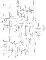
- FIG. 1is a schematic diagram of an apparatus for implementing write assist for SRAM arrays, in accordance with an embodiment of the invention
- FIG. 2is a schematic diagram of an apparatus for implementing write assist for SRAM arrays, in accordance with an alternative embodiment of the invention
- FIG. 3is a schematic diagram of a feedback interlock circuit used to control the timing of the application of negative boost sequence for the write assist circuitry, in accordance with a further embodiment of the invention.
- a negatively boosted write assist apparatusis provided with both a clamping device and an isolation device coupled to a common bit line discharge node.
- the isolation deviceselectively couples the common bitline discharge node to a common boost node driven by a boost capacitor for generating the voltage below the low supply rail value, so as to prevent charge transfer from write data lines to the boost node in unselected banks.
- the clamping deviceprevents the negative boost voltage generated on the boost node from dropping the common discharge node below a certain value that could otherwise activate unselected bit switches.
- a single control function ordinarily used to control both the discharge of the common discharge node and generation of the negative boost voltage on the boost nodeis made independent of one another such that the power dissipated in charging the boost capacitor is further advantageously used to precharge the write bit lines and write data lines, instead of otherwise being wasted.
- an interlock circuitis used to generate feedback that controls the timing of completion of the initial discharge of the common discharge node and the beginning of the negative boost sequence.
- a mimic bit line associated with one or more dummy array cells located along the periphery of the arrayis used in conjunction with control interlock logic that determines a point at which the mimic bit line is very close to ground potential. Once this mimic bit line discharge point is detected, the interlock logic forces the write line discharge control circuitry to cease discharging the common discharge node to ground and apply the negative boost.
- FIG. 1there is shown a schematic diagram of an apparatus 100 for implementing write assist for SRAM arrays, in accordance with an embodiment of the invention.
- the bit line pairs (true and complement) shown in FIG. 1are labeled as BLT_A 0 , BLC_A 0 and BLT_A 1 , BLC_A 1 .
- Each bit line pairincludes a trio of precharge PFETs (collectively designated by 102 ) that are controlled through control signal BLR, as well as a pair of cross-coupled PFETs (collectively designated by 104 ) that serve to reinforce the VDD-precharged level of only one of the bit line pair during a write operation.
- each bit line pairincludes a pair of bit switches 106 , controlled by respective control signals BS 0 , BS 1 .
- the bit switches of a given bit line pairenable writing of individual SRAM cells connected to the bit line pair.
- the write data to be written to selected SRAM cellsis introduced through complementary write data line pairs DLTW 0 , DLCW 0 and DLTW 1 , DLCW 1 in the exemplary embodiment depicted.
- the write data line pairsare also precharged to a logic high rail voltage (V DD ) through PFET devices collectively designated by 108 , and the activation of which is controlled by signal WSEL ⁇ 1 >.
- Global write datais sent to each of the bit line pairs through a pair of NFETs collectively designated by 110 .
- the corresponding global write data NFET control signalse.g., WGBLT ⁇ 0 >, WGBLC ⁇ 0 >
- WGBLT ⁇ 0 >, WGBLC ⁇ 0 >determine which of the true and complementary bit lines of the column will be discharged during the write operation for that column.
- the source terminals of each of the global write data NFETs 110are coupled to a common discharge node 112 labeled WSOURCE in FIG. 1 .
- the common discharge node 112(WSOURCE) is discharged to the nominal low voltage supply rail (e.g., ground) upon activation of a discharge NFET 114 through control signal WSEL ⁇ 0 >.
- the writing of datawould be accomplished once WSOURCE is discharged to ground through the discharge NFET device 114 .
- a negative boostis also used to provide a write assist feature in order to increase the write margin without incurring significant circuit complexity and area penalty.
- FIG. 1further illustrates negative boost circuitry, including a negative boost node 116 (WBOOST), a delay stage (inverter pair) 118 , and a boost capacitor 120 .
- the boost capacitormay be embodied by, for example, a thick oxide FET such as a depletion mode NFET.
- One of the capacitor electrodese.g., the gate terminal of the FET
- the other capacitor electrodee.g., the shorted source/drain terminals of the FET
- the charging of the boost capacitorfollows and is controlled by the same signal WSEL ⁇ 0 >used to activate the discharge NFET device 114 .
- each decoded write data lineapplies a negative voltage on the bitline so as to increase both gate-to-source voltage (V gs ) and drain-to-source voltage (V ds ) on the cell pass gates (not shown), in turn increasing the pass gate conductivity cell write margin by 3 ⁇ or more.
- V gsgate-to-source voltage
- V dsdrain-to-source voltage
- FIG. 1further provides a clamping device 112 , embodied by a diode connected NFET.
- the common discharge node 112(WSOURCE) is prevented from dropping more than (for example) about 250 mV below ground potential, assuming the nominal logic low supply rail is ground.
- the source terminals of unselected NFET bit switchesare not at such a low voltage below ground as to render them conductive when the gate voltage is at a nominally deactivated ground potential.
- the write assist apparatus 100further provides an isolation device 124 to selectively isolate the common discharge node 112 from the negative boost node 116 .
- the isolation device 124embodied by an NFET controlled by signal WSEL ⁇ 1 > in FIG. 1 , prevents charge transfer from write data lines to the negative boost node 116 in unselected banks. Moreover, there is also a resulting performance improvement by keeping the negative boost node voltage between ground and the negative voltage generated thereon. Further, the isolation device 124 helps to eliminate the variability of the boost level generated on the bit lines prior to the boosting operation.
- the bit line pairs and data line pairsare initially charged to the logic high supply value (e.g., V DD ).
- the discharge NFET 114is activated by signal WSEL ⁇ 0 > transitioning from low to high, thus discharging the common discharge node to ground.
- one of the true/complement data lines in a given columnmay be selectively activated through a corresponding NFET 110 .
- all selected bit linesare provided with a path to ground.
- the isolation device NFET 124is activated to couple the common discharge node 112 to the negative boost node 116 .
- the control signal WSEL ⁇ 0 >(through inverter delay stage 118 ) charges the boost capacitor 120 to VDD.
- the resulting positive charge transferred from the boost capacitor 120 to the negative boost node 116is also drained by the discharge NFET 114 .
- NFET 114is deactivated, which also results in the subsequent discharging of the gate terminal of the boost capacitor 120 (also labeled as node BSTRAP in FIG. 1 ), thereby allowing the voltage of the common discharge node 112 to move below ground, the magnitude of which is limited by the clamping device 122 . Any excess negative charge on the common discharge node is dissipated by the diode-connected NFET 122 .
- FIG. 2there is shown a schematic diagram of an apparatus 200 for implementing write assist for SRAM arrays, in accordance with an alternative embodiment of the invention.
- like elements in apparatus 200are designated with the same reference numbers for ease of understanding.
- the apparatus 200may be utilized, for example, in applications where power dissipation is a primary concern.
- the capacitor chargeis essentially wasted.
- the energy used in charging the boost capacitoris further reused to assist in precharging the write data lines and bit lines.
- both the discharge NFET 114 and the boost capacitor 120are coupled directly to the common discharge node 112 (WSOURCE), and thus the use of a separate negative boost node is eliminated.
- WSOURCEcommon discharge node 112
- the control of the discharge NFET 114is now decoupled from the charging of the boost capacitor 120 . That is, the discharge NFET 114 is still controlled by signal WSEL ⁇ 0 >, but charging of the boost capacitor 120 is now controlled by a separate control signal (BOOST) coupled to the input of the inverter delay stage 118 .
- BOOSTseparate control signal
- precharging of the data lines and bit linesis implemented through set of PFET precharge devices, collectively designated by 202 .
- the source terminals of the precharge devices 202are coupled to respective the data lines and bit lines, while the drain terminal thereof are coupled to the common discharge node 112 .
- Control of the PFET precharge devices 202is implemented through a precharge signal WPREN applied to the gate terminals thereof.
- the global write data signalsare (in addition to being applied to global write data NFETs 110 ) applied to another set of PFETs 204 to help maintain the charge on unselected write data lines and bit lines.
- FIG. 3is a schematic diagram of a feedback interlock circuit 300 used to control the timing of the application of negative boost sequence for the write assist circuitry, in accordance with a further embodiment of the invention.
- the interlock circuit 300provides a more precise timing of the turn-off of signal WSEL ⁇ 0 > so that the boost on the write data lines and occurs shortly after the bit lines are discharged to ground by NFET 114 .
- the interlock circuit 300includes a mimic bit line 302 (BLTM) that has write discharge characteristics substantially equivalent to that of a functional bit line (e.g., BLTA 0 ).
- Dummy array edge cellssuch as dummy cell 303 for example, are used to provide the mimic bit line 302 . Because such dummy edge cells are already used in traditional memory devices to isolate and protect the functional array cells from lithographic aberrations, no area penalty is incurred from the use of the mimic bit line.
- the mimic bit line 302is connected to series NFETs N 1 , N 2 and N 3 that emulate the discharge of a functional bit line during a write cycle.
- NFETs N 1 and N 3are controlled by a feedback node 304 in common with the control signal WSEL ⁇ 0 >.
- a precharge PFET P 1is also controlled by the feedback node 304 to precharge the mimic bit line 302 .
- NFET N 3is also coupled to the common discharge node 112 .
- Another NFET N 4in parallel with N 2 , is a margin adjust device controlled by a signal (MAR_ADJ) so as to tune the discharge characteristics of the mimic bit line 302 if need be.
- MAR_ADJa margin adjust device controlled by a signal
- the voltage on the mimic bit line 302is input to trip voltage logic depicted generally at 306 in FIG. 3 .
- the trip voltage logic 306e.g., a NAND gate
- the trip voltage logic 306is configured to trip and generate a logic high output once the voltage on the mimic bit line is close to ground potential.
- This trip signalis inverted by inverter 308 and coupled to PFET P 2 , which in turn causes circuit node 310 to be pulled high.
- Another inverter 312(along with keeper PFET P 3 ) then converts the logic high voltage on node 310 to a logic low voltage at the output thereof, which is also coupled to the feedback node 304 .
- WSEL ⁇ 0 >transitions from high to low, thereby ceasing the discharge of not only the array bit lines and write data lines, but also the mimic bit line 302 .
- the low transition of WSEL ⁇ 0 > that turns off the discharge of the common discharge nodedoes not occur until the bit lines are discharged to ground.
- FIG. 3also illustrates the interface between the interlock circuitry of the mimic bit line and the control circuitry used to implement the write operations of the array, the control circuitry generally designate by 314 .
- the control circuitryincludes a write command signal (WRITE), a subarray select signal (SUBSEL) and address decode signal (SUB_ADDRESS).
- FIG. 4is a graph illustrating the operation of the feedback interlock circuit of FIG. 3 .
- FIG. 4illustrates the timings of the interlock circuit 300 .
- the WRITE commandenables the activation of the WSEL ⁇ 0 > signal that in turn initiates the discharge of the mimic bit line (BLTM).
- BLTMmimic bit line
- the discharging transition of the mimic bit line BLTMis very close (in both slew rate and timing) to that of a functional bit line (BLT 0 ).
- the interlock circuitryshuts off the discharge of all bit lines (i.e., the mimic bit line BLTM and all functional bit lines).
- node BSTRAP(representing the gate voltage of the boost capacitor from FIGS. 1 and 2 ) transitions low to negatively boost WSOURCE as indicated by the arrow in FIG. 4 and produce a negative voltage on the functional bit line BLT 0 .
Landscapes
- Engineering & Computer Science (AREA)
- Microelectronics & Electronic Packaging (AREA)
- Computer Hardware Design (AREA)
- Static Random-Access Memory (AREA)
Abstract
Description
- The present invention relates generally to integrated circuit (IC) memory devices and, more particularly, to an apparatus and method for implementing write assist for static random access memory (SRAM) arrays.
- Memory devices are commonly employed as internal storage areas in a computer or other type of electronic equipment. One specific type of memory used to store data in a computer is random access memory (RAM), such as static RAM (SRAM) or dynamic RAM (DRAM), for example. RAM is typically used as main memory in a computer environment. RAM is generally volatile, in that once power is turned off, all data stored in the RAM is lost.
- A typical SRAM device includes an array of individual SRAM cells. Each SRAM cell is capable of storing a binary voltage value therein, which voltage value represents a logical data bit (e.g., “0” or “1”). One existing configuration for an SRAM cell includes a pair of cross-coupled devices such as inverters. With CMOS (complementary metal oxide semiconductor) technology, the inverters further include a pull-up PFET (p-channel) transistor connected to a complementary pull-down NFET (n-channel) transistor. The inverters, connected in a cross-coupled configuration, act as a latch that stores the data bit therein so long as power is supplied to the memory array. In a conventional six-transistor (6T) cell, a pair of access transistors or pass gates (when activated by a word line) selectively couples the inverters to a pair of complementary bit lines. Other SRAM cell designs may include a different number of transistors, e.g., 4T, 8T, etc.
- The design of SRAM cells has traditionally involved a compromise between the read and write functions of the memory cell to maintain cell stability, read performance and write performance. The transistors which make up the cross-coupled latch must be weak enough to be overdriven during a write operation, while also strong enough to maintain their data value when driving a bit line during a read operation. The access transistors that connect the cross-coupled cell nodes to the true and complement bit lines affect both the stability and performance of the cell. In one-port SRAM cells, a single pair of access transistors is conventionally used for both read and write access to the cell. The gates are driven to a digital value in order to switch the transistors between an on and off state. The optimization of an access for a write operation would drive the reduction of the on-resistance (Ron) for the device. On the other hand, the optimization of an access transistor for a read operation drives an increase in Ronin order to isolate the cell from the bit line capacitance and prevent a cell disturb.
- One recently proposed approach to improving write performance of SRAM devices is to use so-called “negative boosting” to discharge a bit line to a voltage level below the nominal low supply rail value (e.g., ground). In so doing, the pass gates of the SRAM cell coupled to the discharged bit line see a resultant increase in both the gate-to-source and drain-to-source voltages. This negative boosting may allow for an increased margin of 3σ or more (in terms of expected device failures) as compared to more conventional write techniques, wherein the bit line is simply discharged to the value of the nominal low voltage rail (e.g., ground).
- However, notwithstanding the benefits of negative boosting, there are additional problems associated with this technique as presently implemented. For example, in array columns that are unselected (e.g., bit switches are non-conductive to nominally prevent discharging of the associated bit lines), the discharge of a bit line could inadvertently render an inactive bit switch connected thereto conductive if the difference between the gate voltage (e.g., ground) and the source terminal (boosted to a negative voltage) exceeds the threshold voltage of the transistor. In addition, conventional write drivers may allow charge transfer from write data lines to a boost node in unselected memory banks. Furthermore, in existing negative boosting write assist devices, power is wasted when charging a boost capacitor used to generate the voltage below the value of the logic low supply rail. Still another shortcoming of write assist circuitry is the timing between the discharge of the bit line to ground and the subsequent of the negative boost assist to the bit line. If the boost is performed too soon before complete discharge, the bit line will not reach the optimum voltage level below ground potential. Conversely, if performed too late following bit line discharge, the array incurs a cycle-time penalty.
- Accordingly, it would be desirable to be able to take advantage of the performance benefits of negative boost write assistance, but in a manner that also overcomes the above described disadvantages currently associated therewith.
- The foregoing discussed drawbacks and deficiencies of the prior art are overcome or alleviated, in an exemplary embodiment, by an apparatus for implementing a write assist for a memory array, including a common discharge node configured to provide a discharge path for precharged write data lines and bit lines selected during a write operation of the memory array; negative boost circuitry configured to introduce a voltage lower than a nominal logic low supply voltage onto the common discharge node following the discharge of the common discharge node, write data lines and bit lines; and a clamping device coupled to the common discharge node, the clamping device configured to limit the magnitude of negative voltage applied to common discharge node by the negative boost circuitry so as to prevent activation of non-selected bit switches.
- In another embodiment, an interlock apparatus for controlling timing of write assist circuitry associated with a memory array includes a mimic bit line configured to have substantially the same discharge characteristics as write data lines and bit lines associated with the memory array; trip voltage logic coupled to the mimic bit line, the trip voltage logic configured to generate a trip signal upon detection of the mimic bit line being discharged to ground potential; and the trip signal controlling a logic state of a feedback node common to discharge devices of the mimic bit line, and of the write data lines and the bit lines of the memory array such that deactivation of the discharge of the selected write data lines and bit lines of the memory array during a write operation and application of a negative boost voltage to the selected write data lines and bit lines of the memory array does not occur until after the bit lines and write data lines are discharged to ground.
- In still another embodiment, a method for implementing a write assist for a memory array includes configuring a common discharge node to provide a discharge path for precharged write data lines and bit lines selected during a write operation of the memory array; configuring negative boost circuitry to introduce a voltage lower than a nominal logic low supply voltage onto the common discharge node following the discharge of the common discharge node, write data lines and bit lines; and coupling a clamping device to the common discharge node, the clamping device configured to limit the magnitude of negative voltage applied to common discharge node by the negative boost circuitry so as to prevent activation of non-selected bit switches.
- Referring to the exemplary drawings wherein like elements are numbered alike in the several Figures:
FIG. 1 is a schematic diagram of an apparatus for implementing write assist for SRAM arrays, in accordance with an embodiment of the invention;FIG. 2 is a schematic diagram of an apparatus for implementing write assist for SRAM arrays, in accordance with an alternative embodiment of the invention;FIG. 3 is a schematic diagram of a feedback interlock circuit used to control the timing of the application of negative boost sequence for the write assist circuitry, in accordance with a further embodiment of the invention; andFIG. 4 is a graph illustrating the operation of the feedback interlock circuit ofFIG. 3 .- Disclosed herein is an apparatus and method for implementing write assist for SRAM arrays. In one aspect, a negatively boosted write assist apparatus is provided with both a clamping device and an isolation device coupled to a common bit line discharge node. The isolation device selectively couples the common bitline discharge node to a common boost node driven by a boost capacitor for generating the voltage below the low supply rail value, so as to prevent charge transfer from write data lines to the boost node in unselected banks. The clamping device prevents the negative boost voltage generated on the boost node from dropping the common discharge node below a certain value that could otherwise activate unselected bit switches.
- In another aspect, a single control function ordinarily used to control both the discharge of the common discharge node and generation of the negative boost voltage on the boost node is made independent of one another such that the power dissipated in charging the boost capacitor is further advantageously used to precharge the write bit lines and write data lines, instead of otherwise being wasted.
- In still another aspect, an interlock circuit is used to generate feedback that controls the timing of completion of the initial discharge of the common discharge node and the beginning of the negative boost sequence. In lieu of an open-ended timing sequence that could result in process variations causing premature boosting or delayed boosting, a mimic bit line associated with one or more dummy array cells located along the periphery of the array is used in conjunction with control interlock logic that determines a point at which the mimic bit line is very close to ground potential. Once this mimic bit line discharge point is detected, the interlock logic forces the write line discharge control circuitry to cease discharging the common discharge node to ground and apply the negative boost.
- Referring initially to
FIG. 1 , there is shown a schematic diagram of anapparatus 100 for implementing write assist for SRAM arrays, in accordance with an embodiment of the invention. In the exemplary embodiment depicted, only two bit line pairs are illustrated for purposes of simplicity, and thus it will be understood that several additional bit lines are contemplated in a functional SRAM array. The bit line pairs (true and complement) shown inFIG. 1 are labeled as BLT_A0, BLC_A0 and BLT_A1, BLC_A1. Each bit line pair includes a trio of precharge PFETs (collectively designated by102) that are controlled through control signal BLR, as well as a pair of cross-coupled PFETs (collectively designated by104) that serve to reinforce the VDD-precharged level of only one of the bit line pair during a write operation. - As further shown in
FIG. 1 , each bit line pair includes a pair ofbit switches 106, controlled by respective control signals BS0, BS1. The bit switches of a given bit line pair enable writing of individual SRAM cells connected to the bit line pair. The write data to be written to selected SRAM cells is introduced through complementary write data line pairs DLTW0, DLCW0 and DLTW1, DLCW1 in the exemplary embodiment depicted. The write data line pairs are also precharged to a logic high rail voltage (VDD) through PFET devices collectively designated by108, and the activation of which is controlled by signal WSEL<1>. - Global write data is sent to each of the bit line pairs through a pair of NFETs collectively designated by110. For a given write data line pair (e.g., DLTW0, DLCW0) the corresponding global write data NFET control signals (e.g., WGBLT<0>, WGBLC<0>) determine which of the true and complementary bit lines of the column will be discharged during the write operation for that column. Thus, the source terminals of each of the global
write data NFETs 110 are coupled to acommon discharge node 112 labeled WSOURCE inFIG. 1 . The common discharge node112 (WSOURCE) is discharged to the nominal low voltage supply rail (e.g., ground) upon activation of adischarge NFET 114 through control signal WSEL<0>. In a conventional write circuit for an SRAM array, the writing of data would be accomplished once WSOURCE is discharged to ground through thedischarge NFET device 114. However, as mentioned above, a negative boost is also used to provide a write assist feature in order to increase the write margin without incurring significant circuit complexity and area penalty. - More specifically,
FIG. 1 further illustrates negative boost circuitry, including a negative boost node116 (WBOOST), a delay stage (inverter pair)118, and aboost capacitor 120. As known in the art, the boost capacitor may be embodied by, for example, a thick oxide FET such as a depletion mode NFET. One of the capacitor electrodes (e.g., the gate terminal of the FET) is coupled to the output of thedelay stage 118, while the other capacitor electrode (e.g., the shorted source/drain terminals of the FET) is coupled to thenegative boost node 116. In the embodiment depicted, the charging of the boost capacitor (delayed by inverter delay stage118) follows and is controlled by the same signal WSEL<0>used to activate thedischarge NFET device 114. - The mechanism of generating a negative voltage on the
boost node 116 with respect to thecommon discharge node 112 is known in the art, and a detailed description of the same is omitted herein. Notwithstanding, it will be appreciated that the negative boost circuitry is designed to generate a negative voltage with respect to the low voltage rail (e.g., ground) to the extent of about, for example 150 millivolts (mV). Thereby, each decoded write data line applies a negative voltage on the bitline so as to increase both gate-to-source voltage (Vgs) and drain-to-source voltage (Vds) on the cell pass gates (not shown), in turn increasing the pass gate conductivity cell write margin by 3σ or more. - However, as also indicated above, existing negative boost voltage generating devices do not necessarily prevent the boost node from dropping the common discharge node below a certain value that could otherwise activate unselected bit switches. That is, if the negative boost voltage is too large in magnitude, device performance could be adversely affected. Accordingly,
FIG. 1 further provides aclamping device 112, embodied by a diode connected NFET. In so doing, the common discharge node112 (WSOURCE) is prevented from dropping more than (for example) about 250 mV below ground potential, assuming the nominal logic low supply rail is ground. Thereby, the source terminals of unselected NFET bit switches are not at such a low voltage below ground as to render them conductive when the gate voltage is at a nominally deactivated ground potential. - In addition to providing voltage clamping of the
common discharge node 112, thewrite assist apparatus 100 further provides anisolation device 124 to selectively isolate thecommon discharge node 112 from thenegative boost node 116. Theisolation device 124, embodied by an NFET controlled by signal WSEL<1> inFIG. 1 , prevents charge transfer from write data lines to thenegative boost node 116 in unselected banks. Moreover, there is also a resulting performance improvement by keeping the negative boost node voltage between ground and the negative voltage generated thereon. Further, theisolation device 124 helps to eliminate the variability of the boost level generated on the bit lines prior to the boosting operation. - In operation of
apparatus 100, the bit line pairs and data line pairs are initially charged to the logic high supply value (e.g., VDD). After the precharge is complete, thedischarge NFET 114 is activated by signal WSEL<0> transitioning from low to high, thus discharging the common discharge node to ground. Depending upon the data on the global bit line signals, one of the true/complement data lines in a given column may be selectively activated through acorresponding NFET 110. In turn, all selected bit lines are provided with a path to ground. Notably, once the precharge of the data lines is completed (i.e., signal WSEL<1> transitions from low to high), theisolation device NFET 124 is activated to couple thecommon discharge node 112 to thenegative boost node 116. - During the discharge of the
global discharge node 112 to ground, the control signal WSEL<0> (through inverter delay stage118) charges theboost capacitor 120 to VDD. The resulting positive charge transferred from theboost capacitor 120 to thenegative boost node 116 is also drained by thedischarge NFET 114. Once the common discharge node is discharged to ground,NFET 114 is deactivated, which also results in the subsequent discharging of the gate terminal of the boost capacitor120 (also labeled as node BSTRAP inFIG. 1 ), thereby allowing the voltage of thecommon discharge node 112 to move below ground, the magnitude of which is limited by theclamping device 122. Any excess negative charge on the common discharge node is dissipated by the diode-connectedNFET 122. - Referring initially to
FIG. 2 , there is shown a schematic diagram of anapparatus 200 for implementing write assist for SRAM arrays, in accordance with an alternative embodiment of the invention. With respect to the embodiment ofFIG. 1 , like elements inapparatus 200 are designated with the same reference numbers for ease of understanding. Theapparatus 200 may be utilized, for example, in applications where power dissipation is a primary concern. Specifically, in generating the negative boost voltage described above, the capacitor charge is essentially wasted. However, in the embodiment ofFIG. 2 , the energy used in charging the boost capacitor is further reused to assist in precharging the write data lines and bit lines. - More specifically, it will be noted in
FIG. 2 that both the discharge NFET114 and theboost capacitor 120 are coupled directly to the common discharge node112 (WSOURCE), and thus the use of a separate negative boost node is eliminated. Because the generation of the boost voltage is now used in precharging write data and bit lines, the control of thedischarge NFET 114 is now decoupled from the charging of theboost capacitor 120. That is, thedischarge NFET 114 is still controlled by signal WSEL<0>, but charging of theboost capacitor 120 is now controlled by a separate control signal (BOOST) coupled to the input of theinverter delay stage 118. - As further illustrated in
FIG. 2 , precharging of the data lines and bit lines is implemented through set of PFET precharge devices, collectively designated by202. The source terminals of theprecharge devices 202 are coupled to respective the data lines and bit lines, while the drain terminal thereof are coupled to thecommon discharge node 112. Control of the PFETprecharge devices 202 is implemented through a precharge signal WPREN applied to the gate terminals thereof. In addition, the global write data signals are (in addition to being applied to global write data NFETs110) applied to another set ofPFETs 204 to help maintain the charge on unselected write data lines and bit lines. Although theapparatus 200 ofFIG. 2 offers improved power dissipation with respect to the embodiment ofFIG. 1 , one trade off resulting from the use of the boost capacitor charge for precharging is the use of an additional control signal, which results in more complex device control, and ultimately increased cycle time. - With respect to timing, there is also the issue of precisely controlling the timing of turning off the WSEL<0> signal so that the negative boost generated on the
common discharge node 112 occurs shortly after the bit lines are actually discharge to ground throughNFET 114. As indicated above, if the boost is performed too soon before complete discharge of the bit line, the boost circuitry will actually increase the voltage on the discharging bit line instead of lowering it below ground potential (thus preventing the desired write operation). Conversely, if the boost is performed too late following bit line discharge, the array incurs a time penalty. - Accordingly,
FIG. 3 is a schematic diagram of afeedback interlock circuit 300 used to control the timing of the application of negative boost sequence for the write assist circuitry, in accordance with a further embodiment of the invention. In sum, theinterlock circuit 300 provides a more precise timing of the turn-off of signal WSEL<0> so that the boost on the write data lines and occurs shortly after the bit lines are discharged to ground byNFET 114. More specifically, theinterlock circuit 300 includes a mimic bit line302 (BLTM) that has write discharge characteristics substantially equivalent to that of a functional bit line (e.g., BLTA0). Dummy array edge cells, such asdummy cell 303 for example, are used to provide the mimic bit line302. Because such dummy edge cells are already used in traditional memory devices to isolate and protect the functional array cells from lithographic aberrations, no area penalty is incurred from the use of the mimic bit line. - As further shown in
FIG. 3 , the mimic bit line302 is connected to series NFETs N1, N2 and N3 that emulate the discharge of a functional bit line during a write cycle. NFETs N1 and N3 are controlled by afeedback node 304 in common with the control signal WSEL<0>. A precharge PFET P1 is also controlled by thefeedback node 304 to precharge the mimic bit line302. NFET N3 is also coupled to thecommon discharge node 112. Another NFET N4, in parallel with N2, is a margin adjust device controlled by a signal (MAR_ADJ) so as to tune the discharge characteristics of the mimic bit line302 if need be. Thus, during the discharge of the common discharge node such as inFIGS. 1 and 2 , the mimic bit line302 is also discharged in a similar manner. - The voltage on the mimic bit line302 is input to trip voltage logic depicted generally at306 in
FIG. 3 . The trip voltage logic306 (e.g., a NAND gate) is configured to trip and generate a logic high output once the voltage on the mimic bit line is close to ground potential. This trip signal is inverted byinverter 308 and coupled to PFET P2, which in turn causescircuit node 310 to be pulled high. Another inverter312 (along with keeper PFET P3) then converts the logic high voltage onnode 310 to a logic low voltage at the output thereof, which is also coupled to thefeedback node 304. As a result, WSEL<0> transitions from high to low, thereby ceasing the discharge of not only the array bit lines and write data lines, but also the mimic bit line302. In so doing, the low transition of WSEL<0> that turns off the discharge of the common discharge node does not occur until the bit lines are discharged to ground. FIG. 3 also illustrates the interface between the interlock circuitry of the mimic bit line and the control circuitry used to implement the write operations of the array, the control circuitry generally designate by314. As shown, the control circuitry includes a write command signal (WRITE), a subarray select signal (SUBSEL) and address decode signal (SUB_ADDRESS).- Finally,
FIG. 4 is a graph illustrating the operation of the feedback interlock circuit ofFIG. 3 . In particular,FIG. 4 illustrates the timings of theinterlock circuit 300. The WRITE command enables the activation of the WSEL<0> signal that in turn initiates the discharge of the mimic bit line (BLTM). It will be noted fromFIG. 4 that the discharging transition of the mimic bit line BLTM is very close (in both slew rate and timing) to that of a functional bit line (BLT0). Upon reaching the low-level trip point of the mimic bit line (at about 4.55 ns inFIG. 4 ), the interlock circuitry shuts off the discharge of all bit lines (i.e., the mimic bit line BLTM and all functional bit lines). Shortly thereafter, node BSTRAP (representing the gate voltage of the boost capacitor fromFIGS. 1 and 2 ) transitions low to negatively boost WSOURCE as indicated by the arrow inFIG. 4 and produce a negative voltage on the functional bit line BLT0. - While the invention has been described with reference to a preferred embodiment or embodiments, it will be understood by those skilled in the art that various changes may be made and equivalents may be substituted for elements thereof without departing from the scope of the invention. In addition, many modifications may be made to adapt a particular situation or material to the teachings of the invention without departing from the essential scope thereof. Therefore, it is intended that the invention not be limited to the particular embodiment disclosed as the best mode contemplated for carrying out this invention, but that the invention will include all embodiments falling within the scope of the appended claims.
Claims (20)
Priority Applications (1)
| Application Number | Priority Date | Filing Date | Title |
|---|---|---|---|
| US12/048,237US8233342B2 (en) | 2008-03-14 | 2008-03-14 | Apparatus and method for implementing write assist for static random access memory arrays |
Applications Claiming Priority (1)
| Application Number | Priority Date | Filing Date | Title |
|---|---|---|---|
| US12/048,237US8233342B2 (en) | 2008-03-14 | 2008-03-14 | Apparatus and method for implementing write assist for static random access memory arrays |
Publications (2)
| Publication Number | Publication Date |
|---|---|
| US20090235171A1true US20090235171A1 (en) | 2009-09-17 |
| US8233342B2 US8233342B2 (en) | 2012-07-31 |
Family
ID=41064343
Family Applications (1)
| Application Number | Title | Priority Date | Filing Date |
|---|---|---|---|
| US12/048,237Active2031-06-01US8233342B2 (en) | 2008-03-14 | 2008-03-14 | Apparatus and method for implementing write assist for static random access memory arrays |
Country Status (1)
| Country | Link |
|---|---|
| US (1) | US8233342B2 (en) |
Cited By (28)
| Publication number | Priority date | Publication date | Assignee | Title |
|---|---|---|---|---|
| US20120140551A1 (en)* | 2010-12-03 | 2012-06-07 | International Business Machines Corporation | Static random access memory (sram) write assist circuit with leakage suppression and level control |
| US8411518B2 (en) | 2010-12-29 | 2013-04-02 | Stmicroelectronics Pvt. Ltd. | Memory device with boost compensation |
| US8441874B2 (en) | 2010-12-28 | 2013-05-14 | Stmicroelectronics International N.V. | Memory device with robust write assist |
| US8593890B2 (en) | 2012-04-25 | 2013-11-26 | International Business Machines Corporation | Implementing supply and source write assist for SRAM arrays |
| US8806245B2 (en) | 2010-11-04 | 2014-08-12 | Apple Inc. | Memory read timing margin adjustment for a plurality of memory arrays according to predefined delay tables |
| US8842464B2 (en) | 2010-07-23 | 2014-09-23 | Samsung Electronics Co., Ltd. | Static random access memory device including negative voltage level shifter |
| US20150131366A1 (en)* | 2013-11-14 | 2015-05-14 | Taiwan Semiconductor Manufacturing Company Limited | Voltage controller |
| US9087607B2 (en) | 2013-11-12 | 2015-07-21 | International Business Machines Corporation | Implementing sense amplifier for sensing local write driver with bootstrap write assist for SRAM arrays |
| TWI512740B (en)* | 2014-05-07 | 2015-12-11 | Au Optronics Corp | Shift register apparatus and voltage regulating device thereof |
| US20160267952A1 (en)* | 2012-03-15 | 2016-09-15 | Intel Corporation | Negative bitline write assist circuit and method for operating the same |
| US9508420B1 (en)* | 2016-01-28 | 2016-11-29 | Globalfoundries Inc | Voltage-aware adaptive static random access memory (SRAM) write assist circuit |
| US9570156B1 (en) | 2015-08-21 | 2017-02-14 | Globalfoundries Inc. | Data aware write scheme for SRAM |
| US9570155B2 (en)* | 2015-06-09 | 2017-02-14 | Globalfoundries Inc. | Circuit to improve SRAM stability |
| WO2017053068A1 (en)* | 2015-09-22 | 2017-03-30 | Qualcomm Incorporated | Adaptive negative bit line write assist |
| US20170365331A1 (en)* | 2016-06-21 | 2017-12-21 | Arm Limited | Boost Circuit for Memory |
| US9959926B2 (en)* | 2015-10-21 | 2018-05-01 | Avago Technologies General Ip (Singapore) Pte. Ltd. | Method and apparatus for selective write assist using shared boost capacitor |
| WO2018106866A1 (en)* | 2016-12-08 | 2018-06-14 | Ampere Computing Llc | Write assist for memories with resistive bit lines |
| US10020047B2 (en)* | 2016-03-21 | 2018-07-10 | Globalfoundries Inc. | Static random access memory (SRAM) write assist circuit with improved boost |
| US10186312B1 (en)* | 2017-10-12 | 2019-01-22 | Globalfoundries Inc. | Hybrid stack write driver |
| US10395700B1 (en) | 2018-03-20 | 2019-08-27 | Globalfoundries Inc. | Integrated level translator |
| US10522214B2 (en)* | 2016-06-09 | 2019-12-31 | Synopsys, Inc. | Robust negative bit-line and reliability aware write assist |
| US10553274B2 (en)* | 2016-09-21 | 2020-02-04 | Apple Inc. | Low active power write driver with reduced-power boost circuit |
| US11152376B2 (en) | 2017-12-26 | 2021-10-19 | Stmicroelectronics International N.V. | Dual port memory cell with improved access resistance |
| US11176992B2 (en) | 2019-11-04 | 2021-11-16 | Realtek Semiconductor Corporation | Memory write operation apparatus and method |
| DE102021109480A1 (en) | 2020-12-14 | 2022-06-15 | Taiwan Semiconductor Manufacturing Co., Ltd. | STORAGE DEVICE |
| US11404115B2 (en)* | 2020-10-30 | 2022-08-02 | Taiwan Semiconductor Manufacturing Company, Ltd. | Memory with write assist scheme |
| US11462551B2 (en) | 2020-12-14 | 2022-10-04 | Taiwan Semiconductor Manufacturing Company, Ltd. | Memory device |
| WO2023059637A1 (en)* | 2021-10-07 | 2023-04-13 | Micron Technology, Inc. | Boost-assisted memory cell selection in a memory array |
Families Citing this family (18)
| Publication number | Priority date | Publication date | Assignee | Title |
|---|---|---|---|---|
| US8427896B1 (en)* | 2011-11-15 | 2013-04-23 | International Business Machines Corporation | Dynamic wordline assist scheme to improve performance tradeoff in SRAM |
| US9374072B2 (en) | 2012-12-06 | 2016-06-21 | Arm Limited | Post fabrication tuning of an integrated circuit |
| US9058861B2 (en)* | 2012-12-18 | 2015-06-16 | International Business Machines Corporation | Power management SRAM write bit line drive circuit |
| US9070432B2 (en) | 2013-11-12 | 2015-06-30 | Taiwan Semiconductor Manufacturing Co., Ltd. | Negative bitline boost scheme for SRAM write-assist |
| US9142266B2 (en) | 2013-11-19 | 2015-09-22 | Arm Limited | Memory circuitry using write assist voltage boost |
| US9412438B2 (en)* | 2014-01-24 | 2016-08-09 | Taiwan Semiconductor Manufacturing Company, Ltd. | Writing data to a memory cell |
| JP6308831B2 (en)* | 2014-03-25 | 2018-04-11 | ルネサスエレクトロニクス株式会社 | Semiconductor memory device |
| US9548104B1 (en) | 2015-06-30 | 2017-01-17 | International Business Machines Corporation | Boost control to improve SRAM write operation |
| US9431096B1 (en) | 2015-11-17 | 2016-08-30 | International Business Machines Corporation | Hierarchical negative bitline boost write assist for SRAM memory devices |
| US10163524B2 (en) | 2016-06-22 | 2018-12-25 | Darryl G. Walker | Testing a semiconductor device including a voltage detection circuit and temperature detection circuit that can be used to generate read assist and/or write assist in an SRAM circuit portion and method therefor |
| US10497430B2 (en) | 2016-06-22 | 2019-12-03 | Samsung Electronics Co., Ltd. | Semiconductor devices, circuits and methods for read and/or write assist of an SRAM circuit portion based on power supply voltage detection circuits |
| US9852783B1 (en)* | 2016-09-23 | 2017-12-26 | Qualcomm Technologies, Inc. | Metal-oxide semiconductor (MOS) transistor offset-cancelling (OC), zero-sensing (ZS) dead zone, current-latched sense amplifiers (SAs) (CLSAs) (OCZS-SAs) for sensing differential voltages |
| US9761304B1 (en) | 2016-09-27 | 2017-09-12 | International Business Machines Corporation | Write-bitline control in multicore SRAM arrays |
| US9865337B1 (en) | 2017-03-22 | 2018-01-09 | Qualcomm Incorporated | Write data path to reduce charge leakage of negative boost |
| US9875790B1 (en) | 2017-03-31 | 2018-01-23 | Qualcomm Incorporated | Boost charge recycle for low-power memory |
| TWI730745B (en) | 2020-04-30 | 2021-06-11 | 瑞昱半導體股份有限公司 | Device and method for sram write assist |
| US11972793B2 (en) | 2021-09-15 | 2024-04-30 | Mavagail Technology, LLC | Integrated circuit device including an SRAM portion having end power select circuits |
| US12125526B2 (en)* | 2022-03-30 | 2024-10-22 | Qualcomm Incorporated | Memory with bitcell power boosting |
Citations (6)
| Publication number | Priority date | Publication date | Assignee | Title |
|---|---|---|---|---|
| US5576641A (en)* | 1994-05-30 | 1996-11-19 | Kabushiki Kaisha Toshiba | Output buffer |
| US6084454A (en)* | 1998-08-26 | 2000-07-04 | Advanced Micro Devices, Inc. | Start-up circuit for write selects and equilibrates |
| US6671201B2 (en)* | 2001-04-02 | 2003-12-30 | Nec Electronics Corporation | Method for writing data into a semiconductor memory device and semiconductor memory therefor |
| US20070081379A1 (en)* | 2005-09-23 | 2007-04-12 | Texas Instruments, Inc. | Write assist for latch and memory circuits |
| US7292481B2 (en)* | 2003-09-04 | 2007-11-06 | Nec Corporation | Semiconductor storage device |
| US7499325B2 (en)* | 2006-12-21 | 2009-03-03 | Intel Corporation | Flash memory device with improved erase operation |
- 2008
- 2008-03-14USUS12/048,237patent/US8233342B2/enactiveActive
Patent Citations (6)
| Publication number | Priority date | Publication date | Assignee | Title |
|---|---|---|---|---|
| US5576641A (en)* | 1994-05-30 | 1996-11-19 | Kabushiki Kaisha Toshiba | Output buffer |
| US6084454A (en)* | 1998-08-26 | 2000-07-04 | Advanced Micro Devices, Inc. | Start-up circuit for write selects and equilibrates |
| US6671201B2 (en)* | 2001-04-02 | 2003-12-30 | Nec Electronics Corporation | Method for writing data into a semiconductor memory device and semiconductor memory therefor |
| US7292481B2 (en)* | 2003-09-04 | 2007-11-06 | Nec Corporation | Semiconductor storage device |
| US20070081379A1 (en)* | 2005-09-23 | 2007-04-12 | Texas Instruments, Inc. | Write assist for latch and memory circuits |
| US7499325B2 (en)* | 2006-12-21 | 2009-03-03 | Intel Corporation | Flash memory device with improved erase operation |
Cited By (51)
| Publication number | Priority date | Publication date | Assignee | Title |
|---|---|---|---|---|
| US8842464B2 (en) | 2010-07-23 | 2014-09-23 | Samsung Electronics Co., Ltd. | Static random access memory device including negative voltage level shifter |
| US8806245B2 (en) | 2010-11-04 | 2014-08-12 | Apple Inc. | Memory read timing margin adjustment for a plurality of memory arrays according to predefined delay tables |
| CN103229242A (en)* | 2010-12-03 | 2013-07-31 | 国际商业机器公司 | Static random access memory (SRAM) write assist circuit with leakage suppression and level control |
| GB2501997A (en)* | 2010-12-03 | 2013-11-13 | Ibm | Static random access memory (SRAM) write assist circuit with leakage suppression and level control |
| GB2501997B (en)* | 2010-12-03 | 2014-03-26 | Ibm | Static random access memory (SRAM) write assist circuit with leakage suppression and level control |
| US8363453B2 (en)* | 2010-12-03 | 2013-01-29 | International Business Machines Corporation | Static random access memory (SRAM) write assist circuit with leakage suppression and level control |
| WO2012074790A1 (en)* | 2010-12-03 | 2012-06-07 | International Business Machinines Corporation | Static random access memory (sram) write assist circuit with leakage suppression and level control |
| US20120140551A1 (en)* | 2010-12-03 | 2012-06-07 | International Business Machines Corporation | Static random access memory (sram) write assist circuit with leakage suppression and level control |
| US8441874B2 (en) | 2010-12-28 | 2013-05-14 | Stmicroelectronics International N.V. | Memory device with robust write assist |
| US8411518B2 (en) | 2010-12-29 | 2013-04-02 | Stmicroelectronics Pvt. Ltd. | Memory device with boost compensation |
| US20160267952A1 (en)* | 2012-03-15 | 2016-09-15 | Intel Corporation | Negative bitline write assist circuit and method for operating the same |
| US9818460B2 (en)* | 2012-03-15 | 2017-11-14 | Intel Corporation | Negative bitline write assist circuit and method for operating the same |
| US10818326B2 (en) | 2012-03-15 | 2020-10-27 | Intel Corporation | Negative bitline write assist circuit and method for operating the same |
| US10902893B2 (en) | 2012-03-15 | 2021-01-26 | Intel Corporation | Negative bitline write assist circuit and method for operating the same |
| US8593890B2 (en) | 2012-04-25 | 2013-11-26 | International Business Machines Corporation | Implementing supply and source write assist for SRAM arrays |
| US9087607B2 (en) | 2013-11-12 | 2015-07-21 | International Business Machines Corporation | Implementing sense amplifier for sensing local write driver with bootstrap write assist for SRAM arrays |
| US9685223B2 (en)* | 2013-11-14 | 2017-06-20 | Taiwan Semiconductor Manufacturing Company Limited | Voltage controller |
| US20150131366A1 (en)* | 2013-11-14 | 2015-05-14 | Taiwan Semiconductor Manufacturing Company Limited | Voltage controller |
| TWI512740B (en)* | 2014-05-07 | 2015-12-11 | Au Optronics Corp | Shift register apparatus and voltage regulating device thereof |
| US9570155B2 (en)* | 2015-06-09 | 2017-02-14 | Globalfoundries Inc. | Circuit to improve SRAM stability |
| US9570156B1 (en) | 2015-08-21 | 2017-02-14 | Globalfoundries Inc. | Data aware write scheme for SRAM |
| KR20180054779A (en)* | 2015-09-22 | 2018-05-24 | 퀄컴 인코포레이티드 | Adaptive Negative Bitline Write Aid |
| WO2017053068A1 (en)* | 2015-09-22 | 2017-03-30 | Qualcomm Incorporated | Adaptive negative bit line write assist |
| CN108028062A (en)* | 2015-09-22 | 2018-05-11 | 高通股份有限公司 | Adaptive Negative Bitline Write Assist |
| KR102615203B1 (en) | 2015-09-22 | 2023-12-15 | 퀄컴 인코포레이티드 | Adaptive negative bit line writing assistance |
| JP2018527691A (en)* | 2015-09-22 | 2018-09-20 | クアルコム,インコーポレイテッド | Adaptive negative line writing support |
| US9959926B2 (en)* | 2015-10-21 | 2018-05-01 | Avago Technologies General Ip (Singapore) Pte. Ltd. | Method and apparatus for selective write assist using shared boost capacitor |
| CN107017019A (en)* | 2016-01-28 | 2017-08-04 | 格罗方德半导体公司 | Voltage perceives adaptability static random-access memory and writes auxiliary circuit |
| CN107017019B (en)* | 2016-01-28 | 2021-06-01 | 马维尔亚洲私人有限公司 | Voltage-sensing adaptive static random access memory write assist circuit |
| US9508420B1 (en)* | 2016-01-28 | 2016-11-29 | Globalfoundries Inc | Voltage-aware adaptive static random access memory (SRAM) write assist circuit |
| US10020047B2 (en)* | 2016-03-21 | 2018-07-10 | Globalfoundries Inc. | Static random access memory (SRAM) write assist circuit with improved boost |
| US10522214B2 (en)* | 2016-06-09 | 2019-12-31 | Synopsys, Inc. | Robust negative bit-line and reliability aware write assist |
| US20170365331A1 (en)* | 2016-06-21 | 2017-12-21 | Arm Limited | Boost Circuit for Memory |
| US10199092B2 (en)* | 2016-06-21 | 2019-02-05 | Arm Limited | Boost circuit for memory |
| US10553274B2 (en)* | 2016-09-21 | 2020-02-04 | Apple Inc. | Low active power write driver with reduced-power boost circuit |
| US10049725B2 (en) | 2016-12-08 | 2018-08-14 | Ampere Computing Llc | Write assist for memories with resistive bit lines |
| US10109345B2 (en) | 2016-12-08 | 2018-10-23 | Ampere Computing Llc | Write assist for memories with resistive bit lines |
| WO2018106866A1 (en)* | 2016-12-08 | 2018-06-14 | Ampere Computing Llc | Write assist for memories with resistive bit lines |
| US10186312B1 (en)* | 2017-10-12 | 2019-01-22 | Globalfoundries Inc. | Hybrid stack write driver |
| CN109658959A (en)* | 2017-10-12 | 2019-04-19 | 格芯公司 | Hybrid Stacked Write Drives |
| TWI677869B (en)* | 2017-10-12 | 2019-11-21 | 美商格芯(美國)集成電路科技有限公司 | Hybrid stack write driver |
| US11532633B2 (en) | 2017-12-26 | 2022-12-20 | Stmicroelectronics International N.V. | Dual port memory cell with improved access resistance |
| US11152376B2 (en) | 2017-12-26 | 2021-10-19 | Stmicroelectronics International N.V. | Dual port memory cell with improved access resistance |
| US11889675B2 (en) | 2017-12-26 | 2024-01-30 | Stmicroelectronics International N.V. | Dual port memory cell with improved access resistance |
| US10395700B1 (en) | 2018-03-20 | 2019-08-27 | Globalfoundries Inc. | Integrated level translator |
| US11176992B2 (en) | 2019-11-04 | 2021-11-16 | Realtek Semiconductor Corporation | Memory write operation apparatus and method |
| US11404115B2 (en)* | 2020-10-30 | 2022-08-02 | Taiwan Semiconductor Manufacturing Company, Ltd. | Memory with write assist scheme |
| US11462551B2 (en) | 2020-12-14 | 2022-10-04 | Taiwan Semiconductor Manufacturing Company, Ltd. | Memory device |
| DE102021109480A1 (en) | 2020-12-14 | 2022-06-15 | Taiwan Semiconductor Manufacturing Co., Ltd. | STORAGE DEVICE |
| US12193206B2 (en) | 2020-12-14 | 2025-01-07 | Taiwan Semiconductor Manufacturing Company, Ltd. | Memory device |
| WO2023059637A1 (en)* | 2021-10-07 | 2023-04-13 | Micron Technology, Inc. | Boost-assisted memory cell selection in a memory array |
Also Published As
| Publication number | Publication date |
|---|---|
| US8233342B2 (en) | 2012-07-31 |
Similar Documents
| Publication | Publication Date | Title |
|---|---|---|
| US8233342B2 (en) | Apparatus and method for implementing write assist for static random access memory arrays | |
| US10783956B2 (en) | Tunable negative bitline write assist and boost attenuation circuit | |
| CN111164691B (en) | Area efficient write data path circuit for SRAM yield enhancement | |
| JP2006318642A (en) | Dynamic random access memory | |
| US6801463B2 (en) | Method and apparatus for leakage compensation with full Vcc pre-charge | |
| US9978443B2 (en) | Method of controlling auxiliary branches for SRAM cell | |
| US9837144B1 (en) | Apparatus and method for controlling boost capacitance for low power memory circuits | |
| US9865334B2 (en) | Efficient bitline driven one-sided power collapse write-assist design for SRAMs | |
| KR20010073605A (en) | High voltage discharge circuit of a semiconductor memory device | |
| US8830784B2 (en) | Negative word line driver for semiconductor memories | |
| US7203097B2 (en) | Method of operating a semiconductor device and the semiconductor device | |
| US7376029B2 (en) | Semiconductor memory devices including precharge circuit and methods for precharging | |
| TW202213337A (en) | Boost circuit | |
| US20130308399A1 (en) | Write self timing circuitry for self-timed memory | |
| US11610612B2 (en) | High speed SRAM using enhance wordline/global buffer drive | |
| US11676652B2 (en) | Wordline boost driver | |
| TWI699764B (en) | Memory write operation apparatus and method | |
| US11929116B2 (en) | Memory device having a negative voltage circuit | |
| US20240071480A1 (en) | Process and temperature compensated word line underdrive scheme for sram |
Legal Events
| Date | Code | Title | Description |
|---|---|---|---|
| AS | Assignment | Owner name:INTERNATIONAL BUSINESS MACHINES CORPORATION, NEW Y Free format text:ASSIGNMENT OF ASSIGNORS INTEREST;ASSIGNORS:ADAMS, CARL A.;BRACERAS, GEORGE M.;PILO, HAROLD;AND OTHERS;REEL/FRAME:020649/0614;SIGNING DATES FROM 20080307 TO 20080310 Owner name:INTERNATIONAL BUSINESS MACHINES CORPORATION, NEW Y Free format text:ASSIGNMENT OF ASSIGNORS INTEREST;ASSIGNORS:ADAMS, CARL A.;BRACERAS, GEORGE M.;PILO, HAROLD;AND OTHERS;SIGNING DATES FROM 20080307 TO 20080310;REEL/FRAME:020649/0614 | |
| STCF | Information on status: patent grant | Free format text:PATENTED CASE | |
| AS | Assignment | Owner name:GLOBALFOUNDRIES U.S. 2 LLC, NEW YORK Free format text:ASSIGNMENT OF ASSIGNORS INTEREST;ASSIGNOR:INTERNATIONAL BUSINESS MACHINES CORPORATION;REEL/FRAME:036550/0001 Effective date:20150629 | |
| AS | Assignment | Owner name:GLOBALFOUNDRIES INC., CAYMAN ISLANDS Free format text:ASSIGNMENT OF ASSIGNORS INTEREST;ASSIGNORS:GLOBALFOUNDRIES U.S. 2 LLC;GLOBALFOUNDRIES U.S. INC.;REEL/FRAME:036779/0001 Effective date:20150910 | |
| FPAY | Fee payment | Year of fee payment:4 | |
| AS | Assignment | Owner name:WILMINGTON TRUST, NATIONAL ASSOCIATION, DELAWARE Free format text:SECURITY AGREEMENT;ASSIGNOR:GLOBALFOUNDRIES INC.;REEL/FRAME:049490/0001 Effective date:20181127 | |
| AS | Assignment | Owner name:GLOBALFOUNDRIES U.S. INC., CALIFORNIA Free format text:ASSIGNMENT OF ASSIGNORS INTEREST;ASSIGNOR:GLOBALFOUNDRIES INC.;REEL/FRAME:050122/0001 Effective date:20190821 | |
| AS | Assignment | Owner name:MARVELL INTERNATIONAL LTD., BERMUDA Free format text:ASSIGNMENT OF ASSIGNORS INTEREST;ASSIGNOR:GLOBALFOUNDRIES U.S. INC.;REEL/FRAME:051070/0625 Effective date:20191105 | |
| MAFP | Maintenance fee payment | Free format text:PAYMENT OF MAINTENANCE FEE, 8TH YEAR, LARGE ENTITY (ORIGINAL EVENT CODE: M1552); ENTITY STATUS OF PATENT OWNER: LARGE ENTITY Year of fee payment:8 | |
| AS | Assignment | Owner name:CAVIUM INTERNATIONAL, CAYMAN ISLANDS Free format text:ASSIGNMENT OF ASSIGNORS INTEREST;ASSIGNOR:MARVELL INTERNATIONAL LTD.;REEL/FRAME:052918/0001 Effective date:20191231 | |
| AS | Assignment | Owner name:MARVELL ASIA PTE, LTD., SINGAPORE Free format text:ASSIGNMENT OF ASSIGNORS INTEREST;ASSIGNOR:CAVIUM INTERNATIONAL;REEL/FRAME:053475/0001 Effective date:20191231 | |
| AS | Assignment | Owner name:GLOBALFOUNDRIES INC., CAYMAN ISLANDS Free format text:RELEASE BY SECURED PARTY;ASSIGNOR:WILMINGTON TRUST, NATIONAL ASSOCIATION;REEL/FRAME:054636/0001 Effective date:20201117 | |
| MAFP | Maintenance fee payment | Free format text:PAYMENT OF MAINTENANCE FEE, 12TH YEAR, LARGE ENTITY (ORIGINAL EVENT CODE: M1553); ENTITY STATUS OF PATENT OWNER: LARGE ENTITY Year of fee payment:12 |