US20090233449A1 - Etching chamber with subchamber - Google Patents
Etching chamber with subchamberDownload PDFInfo
- Publication number
- US20090233449A1 US20090233449A1US11/816,760US81676006AUS2009233449A1US 20090233449 A1US20090233449 A1US 20090233449A1US 81676006 AUS81676006 AUS 81676006AUS 2009233449 A1US2009233449 A1US 2009233449A1
- Authority
- US
- United States
- Prior art keywords
- sample
- chamber
- semiconductor wafer
- subchamber
- assembly
- Prior art date
- Legal status (The legal status is an assumption and is not a legal conclusion. Google has not performed a legal analysis and makes no representation as to the accuracy of the status listed.)
- Granted
Links
- 238000005530etchingMethods0.000titleclaimsabstractdescription61
- 239000004065semiconductorSubstances0.000claimsabstractdescription68
- 230000007246mechanismEffects0.000claimsdescription17
- 238000000034methodMethods0.000claimsdescription8
- 238000004891communicationMethods0.000claimsdescription4
- 235000012431wafersNutrition0.000description67
- 239000007789gasSubstances0.000description45
- BLIQUJLAJXRXSG-UHFFFAOYSA-N1-benzyl-3-(trifluoromethyl)pyrrolidin-1-ium-3-carboxylateChemical compoundC1C(C(=O)O)(C(F)(F)F)CCN1CC1=CC=CC=C1BLIQUJLAJXRXSG-UHFFFAOYSA-N0.000description4
- 239000000463materialSubstances0.000description3
- 230000004075alterationEffects0.000description2
- 239000012530fluidSubstances0.000description2
- 229910052734heliumInorganic materials0.000description2
- 239000001307heliumSubstances0.000description2
- SWQJXJOGLNCZEY-UHFFFAOYSA-Nhelium atomChemical compound[He]SWQJXJOGLNCZEY-UHFFFAOYSA-N0.000description2
- 238000012986modificationMethods0.000description2
- 230000004048modificationEffects0.000description2
- 238000003825pressingMethods0.000description2
- 230000008569processEffects0.000description2
- 238000012545processingMethods0.000description2
- 238000007789sealingMethods0.000description2
- 239000002699waste materialSubstances0.000description2
- ZOKXTWBITQBERF-UHFFFAOYSA-NMolybdenumChemical compound[Mo]ZOKXTWBITQBERF-UHFFFAOYSA-N0.000description1
- 230000009471actionEffects0.000description1
- 230000008901benefitEffects0.000description1
- 230000015572biosynthetic processEffects0.000description1
- 238000013461designMethods0.000description1
- 238000010586diagramMethods0.000description1
- 238000004519manufacturing processMethods0.000description1
- 230000013011matingEffects0.000description1
- 229910052750molybdenumInorganic materials0.000description1
- 239000011733molybdenumSubstances0.000description1
- NJPPVKZQTLUDBO-UHFFFAOYSA-NnovaluronChemical compoundC1=C(Cl)C(OC(F)(F)C(OC(F)(F)F)F)=CC=C1NC(=O)NC(=O)C1=C(F)C=CC=C1FNJPPVKZQTLUDBO-UHFFFAOYSA-N0.000description1
- 230000000750progressive effectEffects0.000description1
- 229910052710siliconInorganic materials0.000description1
- 239000010703siliconSubstances0.000description1
- 239000011343solid materialSubstances0.000description1
- 239000000758substrateSubstances0.000description1
Images


Classifications
- H—ELECTRICITY
- H01—ELECTRIC ELEMENTS
- H01L—SEMICONDUCTOR DEVICES NOT COVERED BY CLASS H10
- H01L21/00—Processes or apparatus adapted for the manufacture or treatment of semiconductor or solid state devices or of parts thereof
- H01L21/02—Manufacture or treatment of semiconductor devices or of parts thereof
- H01L21/04—Manufacture or treatment of semiconductor devices or of parts thereof the devices having potential barriers, e.g. a PN junction, depletion layer or carrier concentration layer
- H01L21/18—Manufacture or treatment of semiconductor devices or of parts thereof the devices having potential barriers, e.g. a PN junction, depletion layer or carrier concentration layer the devices having semiconductor bodies comprising elements of Group IV of the Periodic Table or AIIIBV compounds with or without impurities, e.g. doping materials
- H01L21/30—Treatment of semiconductor bodies using processes or apparatus not provided for in groups H01L21/20 - H01L21/26
- H01L21/302—Treatment of semiconductor bodies using processes or apparatus not provided for in groups H01L21/20 - H01L21/26 to change their surface-physical characteristics or shape, e.g. etching, polishing, cutting
- H01L21/306—Chemical or electrical treatment, e.g. electrolytic etching
- H01L21/3065—Plasma etching; Reactive-ion etching
- H—ELECTRICITY
- H01—ELECTRIC ELEMENTS
- H01L—SEMICONDUCTOR DEVICES NOT COVERED BY CLASS H10
- H01L21/00—Processes or apparatus adapted for the manufacture or treatment of semiconductor or solid state devices or of parts thereof
- H01L21/67—Apparatus specially adapted for handling semiconductor or electric solid state devices during manufacture or treatment thereof; Apparatus specially adapted for handling wafers during manufacture or treatment of semiconductor or electric solid state devices or components ; Apparatus not specifically provided for elsewhere
- H01L21/67005—Apparatus not specifically provided for elsewhere
- H01L21/67011—Apparatus for manufacture or treatment
- H01L21/67017—Apparatus for fluid treatment
- H01L21/67063—Apparatus for fluid treatment for etching
- H01L21/67069—Apparatus for fluid treatment for etching for drying etching
- H—ELECTRICITY
- H01—ELECTRIC ELEMENTS
- H01L—SEMICONDUCTOR DEVICES NOT COVERED BY CLASS H10
- H01L21/00—Processes or apparatus adapted for the manufacture or treatment of semiconductor or solid state devices or of parts thereof
- H01L21/67—Apparatus specially adapted for handling semiconductor or electric solid state devices during manufacture or treatment thereof; Apparatus specially adapted for handling wafers during manufacture or treatment of semiconductor or electric solid state devices or components ; Apparatus not specifically provided for elsewhere
- H01L21/67005—Apparatus not specifically provided for elsewhere
- H01L21/67011—Apparatus for manufacture or treatment
- H01L21/67017—Apparatus for fluid treatment
- H01L21/67063—Apparatus for fluid treatment for etching
- H—ELECTRICITY
- H01—ELECTRIC ELEMENTS
- H01L—SEMICONDUCTOR DEVICES NOT COVERED BY CLASS H10
- H01L21/00—Processes or apparatus adapted for the manufacture or treatment of semiconductor or solid state devices or of parts thereof
- H01L21/67—Apparatus specially adapted for handling semiconductor or electric solid state devices during manufacture or treatment thereof; Apparatus specially adapted for handling wafers during manufacture or treatment of semiconductor or electric solid state devices or components ; Apparatus not specifically provided for elsewhere
- H01L21/677—Apparatus specially adapted for handling semiconductor or electric solid state devices during manufacture or treatment thereof; Apparatus specially adapted for handling wafers during manufacture or treatment of semiconductor or electric solid state devices or components ; Apparatus not specifically provided for elsewhere for conveying, e.g. between different workstations
- H01L21/67739—Apparatus specially adapted for handling semiconductor or electric solid state devices during manufacture or treatment thereof; Apparatus specially adapted for handling wafers during manufacture or treatment of semiconductor or electric solid state devices or components ; Apparatus not specifically provided for elsewhere for conveying, e.g. between different workstations into and out of processing chamber
- H01L21/67745—Apparatus specially adapted for handling semiconductor or electric solid state devices during manufacture or treatment thereof; Apparatus specially adapted for handling wafers during manufacture or treatment of semiconductor or electric solid state devices or components ; Apparatus not specifically provided for elsewhere for conveying, e.g. between different workstations into and out of processing chamber characterized by movements or sequence of movements of transfer devices
- H—ELECTRICITY
- H01—ELECTRIC ELEMENTS
- H01L—SEMICONDUCTOR DEVICES NOT COVERED BY CLASS H10
- H01L21/00—Processes or apparatus adapted for the manufacture or treatment of semiconductor or solid state devices or of parts thereof
- H01L21/67—Apparatus specially adapted for handling semiconductor or electric solid state devices during manufacture or treatment thereof; Apparatus specially adapted for handling wafers during manufacture or treatment of semiconductor or electric solid state devices or components ; Apparatus not specifically provided for elsewhere
- H01L21/677—Apparatus specially adapted for handling semiconductor or electric solid state devices during manufacture or treatment thereof; Apparatus specially adapted for handling wafers during manufacture or treatment of semiconductor or electric solid state devices or components ; Apparatus not specifically provided for elsewhere for conveying, e.g. between different workstations
- H01L21/67739—Apparatus specially adapted for handling semiconductor or electric solid state devices during manufacture or treatment thereof; Apparatus specially adapted for handling wafers during manufacture or treatment of semiconductor or electric solid state devices or components ; Apparatus not specifically provided for elsewhere for conveying, e.g. between different workstations into and out of processing chamber
- H01L21/67751—Apparatus specially adapted for handling semiconductor or electric solid state devices during manufacture or treatment thereof; Apparatus specially adapted for handling wafers during manufacture or treatment of semiconductor or electric solid state devices or components ; Apparatus not specifically provided for elsewhere for conveying, e.g. between different workstations into and out of processing chamber vertical transfer of a single workpiece
Definitions
- Vapor etching of semiconductor materials and/or substratesis accomplished using gases, such as xenon difluoride. Specifically, in xenon difluoride etching, xenon difluoride gas reacts with solid materials, such as silicon and molybdenum, such that the materials are converted to a gas phase. The removal of these materials is known as etching.
- MESCModular Equipment Standards Committee
- MESC compatible chambershave a wafer loading port on one side, the chamber is inherently non-symmetric. Such asymmetry can lead to non-uniform etching of the wafer since the gas is not distributed axisymmetrically about the wafer.
- a chambersuch as, without limitation, an MESC compatible etching chamber or other etching chamber with a port on the side for loading, which has a subchamber assembly inside that creates a reduced chamber volume, is desirably axisymmetric shaped, that maximizes utilization of the etching gas and improves wafer etch uniformity.
- the inventionis a semiconductor wafer or sample etching system having a first chamber including a loading port for the passage of a semiconductor wafer or sample between an exterior and an interior of the first chamber having a first volume and a vacuum port in communication with the interior of the first chamber.
- a wafer or sample holderis disposed in the interior of the first chamber for supporting the semiconductor wafer or sample passed through the loading port.
- a subchamber assemblyis disposed within the first chamber. The subchamber assembly is moveable between an open position, wherein the semiconductor wafer or sample passed through the loading port can be loaded on the sample holder, and a closed position, wherein the combination of the subchamber assembly and the first chamber form a second chamber defining a second, smaller volume that includes the sample holder and the vacuum port.
- the etching systemcan include means for lowering and lifting the semiconductor wafer or sample to and from the sample holder.
- the means for lowering and liftingcan include means for supporting the semiconductor wafer or sample along an edge thereof during the lowering and lifting thereof, a pneumatic or hydraulic mechanism for lowering and lifting the semiconductor wafer or sample, and/or an electric actuator for lowering and lifting the semiconductor wafer or sample.
- the etching systemcan include an etching gas port in the subchamber assembly for the passage of etching gas into the second chamber and means for passing the etching gas to the etching gas port.
- Meanscan be provided for clamping or holding the semiconductor wafer or sample to the sample holder, especially when the subchamber assembly is in the closed position. Means can also be provided for introducing a gas between the semiconductor wafer or sample and the sample holder when the semiconductor wafer or sample is positioned on the sample holder.
- a first sealcan be disposed between the subchamber assembly and the first chamber for avoiding the passage of gas therebetween when the subchamber assembly is in the closed position.
- An adaptor ringcan be disposed between the subchamber assembly and the first chamber.
- a second sealcan be disposed between the adaptor ring and the first chamber for avoiding the passage of gas therebetween when the subchamber assembly is in the closed position.
- the inventionis also a method of etching a semiconductor wafer or sample comprising (a) causing a semiconductor wafer or sample to be placed on a sample holder in a first chamber; (b) enclosing the semiconductor wafer or sample on the sample holder within a second chamber inside the first chamber; (c) evacuating gas from the second chamber; and (d) introducing an etching gas into the second chamber but not into the first chamber.
- the methodcan also include clamping the semiconductor wafer or sample to the sample holder and/or introducing a thermally-conductive gas between the semiconductor wafer or sample and the sample holder.
- the first chambercan have a first volume and the second chamber can have a second, smaller volume that is coextensive with the first volume.
- the inventionis a semiconductor wafer or sample etching system that includes a first chamber, a sample holder in the first chamber, and a subchamber assembly inside the first chamber.
- the subchamber assemblycan be moved between a first position that permits introduction or removal of a semiconductor wafer or sample onto or from the sample holder and second position, wherein the combination of the subchamber assembly and the first chamber define an enclosed second chamber inside the first chamber.
- Meanscan be provided for lowering and lifting the semiconductor wafer or sample to and from the sample holder.
- the means for lowering and liftingcan include means for supporting the semiconductor wafer or sample along an edge thereof during the lowering and lifting thereof, a pneumatic or hydraulic mechanism for lowering and lifting the semiconductor wafer or sample semiconductor wafer or sample, and/or an electric actuator for lowering and lifting the semiconductor wafer or sample.
- Meanscan also be provided for passing etching gas into the second chamber, but not the first chamber.
- Meanscan also be provided for holding the semiconductor wafer or sample to the sample holder, especially when the subchamber assembly is in the closed position.
- Meanscan also be provided for introducing a gas between the semiconductor wafer or sample and the sample holder when the semiconductor wafer or sample is positioned on the sample holder.
- At least one sealcan be disposed between the subchamber assembly and the first chamber for avoiding the passage of gas therebetween when the subchamber assembly is in the closed position.
- An adaptor ringcan be disposed between the subchamber assembly and the first chamber, whereupon the subchamber assembly in the closed position contacts the adaptor ring which, in turn, contacts the first chamber.
- FIG. 1is a cross-sectional perspective view of prior art MESC compatible chamber block and lid including therein a subchamber assembly in accordance with the present invention
- FIG. 2is a sectional view taken along line II-II in FIG. 1 ;
- FIG. 3is a block diagram of a flow of etching gas through the subchamber assembly shown in FIG. 1 ;
- FIGS. 4-8are cross-sectional views of the chamber block and subchamber assembly shown in FIG. 1 showing the progressive loading of a semiconductor wafer or sample on a sample holder thereof and the formation of a sealed chamber around the sample holder with the semiconductor wafer or sample loaded thereon;
- FIG. 9is a cross-sectional perspective view of the semiconductor wafer or sample positioned on the sample holder of the sealed chamber shown in FIG. 8 including vertical and horizontal channels in fluid communication with a port of the subchamber assembly for the introducing of etchant gas into the sealed chamber;
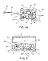
- FIG. 10is a cross-sectional perspective view of another embodiment of the chamber block including the subchamber assembly and an adaptor ring, with the subchamber assembly in the open position;
- FIG. 11is a cross-sectional view of the chamber block and subchamber assembly shown in FIG. 10 , with the subchamber assembly in the closed position against the adaptor ring;
- FIG. 12is a cross-sectional perspective view of the chamber block and subchamber assembly, wherein the wafer clamping tabs utilized to clamp the semiconductor wafer or sample to the sample holder shown in FIG. 8 are replaced with a weight and clamping fingers;
- FIG. 13is a cross-sectional view of the chamber block and subchamber assembly shown in FIG. 12 , with the semiconductor wafer or sample positioned for loading onto the sample holder;
- FIG. 14is a cross-sectional perspective view of the chamber block and subchamber assembly of FIGS. 12 and 13 , with the semiconductor wafer or sample positioned on the sample holder in the sealed chamber formed by the subchamber assembly in the closed position.
- a MESC compatible or other side-loaded etching chamberincludes a chamber block 103 and a lid 102 .
- Chamber block 103includes a sample loading port 108 and a vacuum port 113 which can be coupled to a suitable source of vacuum, e.g., vacuum pump 128 in FIG. 3 , which is operative for drawing a vacuum on an interior of chamber block 103 .
- the interior of chamber block 103defines a first volume.
- a sample loading arm 100with a semiconductor wafer or sample 101 , a subchamber assembly 106 having a gas inlet port 110 in a lid thereof, one or more optional sample clamping tabs 107 , a sample lifting means 105 and a subchamber seal 111 .
- gas inlet port 110 in the lid of subchamber assembly 106is not to be construed as limiting the invention.
- a lifting mechanism 112is desirably coupled between chamber block 103 and a lifting/lowering means 114 , shown in FIG. 4 , which is operative for raising and lowering subchamber assembly 106 , and any components attached thereto, via lifting mechanism 112 .
- lifting mechanism 112desirably comprises a pair of rods coupled between subchamber assembly 106 , desirably a lid of subchamber assembly 106 , and lifting/lower means 114 via a pair of slide channels defined through a floor of chamber block 103 .
- a suitable gas tight seal(not shown) can be disposed between each rod and its corresponding slide channel to avoid the passage of gas thereby.
- lifting mechanism 112comprising a pair of rods slideable in slide channels, however, is not to be construed as limiting the invention since it is envisioned that lifting mechanism 112 can be implemented in any manner deemed suitable and/or desirable by one of ordinary skill in the art.
- FIG. 1also shows a sample holder 104 , such as, without limitation, a wafer chuck, desirably temperature controlled, with an optional gas connection 109 .
- Gas connection 109is configured for introducing a thermal conduction gas, such as helium, between sample 101 and sample holder 104 when sample 101 is positioned on sample holder 104 to improve thermal conduction therebetween.
- a flexible gas seal 117shown in phantom in FIG. 1 , can be disposed between sample 101 positioned on sample holder 104 .
- sample holder 104includes notches 116 defined therein and sample lifting means 105 includes corresponding tabs 115 .
- tabs 115 defined on sample lifting means 105are received in notches 116 defined in or through sample holder 104 .
- Tabs 115provide wafer lift capability known as edge lift.
- etching gasflows from a source container 120 , through a gas control 122 , e.g., a valve, a series of valves, a pressure controller, an intermediate expansion chamber of any of the types disclosed in U.S. Pat. No. 6,887,337 to Lebouitz et al., which is incorporated herein by reference, a flow controller, or any combination of these components, through subchamber assembly 106 (block 124 ), which, in combination with chamber block 103 , can form a sealed chamber 130 (shown best in FIGS. 8 and 9 ), through a vacuum controller 126 , which may be a valve, a series of valves, a pressure controller, a flow controller or any combination of these components, and then through a vacuum pump 128 .
- a gas control 122e.g., a valve, a series of valves, a pressure controller, an intermediate expansion chamber of any of the types disclosed in U.S. Pat. No. 6,887,337 to Lebouitz
- FIG. 4shows subchamber assembly 106 , sample lifting means 105 , subchamber seal 111 , wafer clamping tabs 107 and lifting mechanism 112 raised into a load or open position via lifting/lowering means 114 , such as, without limitation, a suitable pneumatic or hydraulic mechanism or an electric actuator.
- sample lifting means 105 , subchamber assembly seal 111 and wafer clamping tabs 107are coupled to subchamber assembly 106 which, in turn, is coupled to lifting mechanism 112 .
- thisis not to be construed as limiting the invention since it is envisioned that sample lifting means 105 and wafer clamping tabs 107 can be coupled to lifting mechanism 112 in any suitable and/or desirable manner.
- subchamber assembly seal 111can alternatively be located on the mating face of a floor of chamber block 103 where the lower end of subchamber assembly 106 contacts to form the sealed chamber 130 , shown best in FIGS. 8 and 9 .
- sample 101is shown positioned between subchamber assembly seal 111 and sample lifting means 105 outside the periphery of subchamber assembly seal 111 by sample loading arm 100 .
- sample 101is positioned beneath, desirably concentric, with subchamber assembly 106 by sample loading arm 100 .
- FIG. 6shows sample loading arm 100 in the same position as in FIG. 5 but with subchamber assembly 106 , sample lifting means 105 , subchamber seal 111 , and wafer clamping tabs 107 moved by lifting/lowering means 114 via lifting mechanism 112 in a vertical direction away from sample holder 104 , whereupon tabs 115 of sample lifting means 105 lift sample 101 off of sample loading arm 100 via the edge of sample 101 .
- This lifting actionis helpful in that sample loading arm 100 does not need to have vertical motion capability.
- wafer arm 100is retracted from chamber block 103 .
- chamber block 103includes a door (not shown) for closing and sealing loading port 108 after sample 101 has been loaded onto sample holder 104 .
- sample clamping tabs 107are flexible and have a spring memory in a vertical direction whereupon they can clamp sample 101 to sample holder 104 with spring force related to the diameter and thickness of sample 101 .
- thisis not to be construed as limiting the invention.
- Adding a thermally-conductive gas, such as helium, through gas connection 109 when sample 101 is loaded on sample holder 104can further improve thermal conduction between sample 101 and sample holder 104 . Clamping sample 101 to sample holder 104 also avoids etching gas from reaching the rear of sample 101 .
- a thermally-conductive gassuch as helium
- FIG. 9shows one non-limiting embodiment wherein etching gas flows through a vertical channel 132 defined in a rod of lifting mechanism 112 in direct fluid communication with a horizontal channel 134 in the lid of subchamber assembly 106 before exiting port 110 .
- sample 101is removed from the etching chamber by reversing the procedures used to load sample 101 on sample holder 104 .
- FIG. 10shows that a reduced volume subchamber assembly 106 N is easily implemented maximizing the utilization of etching gas.
- This reduced volume subchamber assembly 106 Nincludes appropriately sized components, such as, without limitation, sample lifting means 105 , subchamber seal 111 , wafer clamping tabs 107 , and lifting mechanism 112 .
- a reduced-sized sample holder 104 ′can also be employed in combination with an optional adaptor sealing ring 140 mounted on a floor of chamber block 103 around sample holder 104 ′.
- Adaptor ring 140includes around the base thereof a seal 141 configured to engage the floor of chamber block 103 to form a seal between adaptor ring 140 and the floor of chamber block 103 to avoid the passage of etching gas from sealed chamber 130 .
- FIG. 11shows a cross section of the chamber block 103 shown in FIG. 10 looking directly from the side with subchamber assembly 106 in the closed position pressing subchamber seal 111 into contact with a top surface of adaptor ring 140 and, thereby, pressing seal 141 into contact with the floor of chamber block 103 to form seals therebetween that avoid the passage of etching gas from sealed chamber 130 .
- FIGS. 12-14show another means for clamping semiconductor wafer or sample 101 to sample holder 104 by way of a weight 150 .
- Weight 150provides the necessary downward force to clamp sample 101 to sample holder 104 via clamping fingers 152 arranged around an inner periphery of weight 150 .
- An advantage of using weight 150 for clampingis that the clamping force will be independent of wafer diameter, which is typically not the case when using a spring-based clamping design, e.g., wafer clamping tabs 107 .
- Weight 150is able to move vertically inside of the subchamber assembly 106 so that clamping fingers 152 can apply a downward force on sample 101 .
- vertical sliding motion between weight 150 and subchamber assembly 106is accomplished via slides 154 which are distributed between weight 150 and subchamber assembly 106 and which are accommodated by grooves 158 in subchamber assembly 106 .
- the downward motion of weight 150is restricted by a retaining ring 156 which, thereby, enables weight 150 to be raised and lowered from and to sample holder 104 in concert with the raising and lowering of subchamber assembly 106 by lifting/lowering means 114 . As shown in FIG.
- slides 154enable subchamber assembly 103 to move subchamber seal 111 into contact with a floor of chamber block 103 after clamping fingers 152 of weight 150 have engaged a top surface of sample 101 , thereby clamping sample 101 to sample holder 104 .
- sample lifting means 105can be replaced by other suitable means, such as so-called wafer lift pins 144 , shown in phantom in FIG. 13 , slidably received in channels 146 formed in sample holder 104 and coupled to lifting/lowering means 114 .
- wafer lift pins 144shown in phantom in FIG. 13
- the vertical motion of these wafer lift pins 144can be controlled to raise and lower sample 101 away and toward sample holder 104 during loading and unloading of sample 101 on sample holder 104 .
- sample lifting means 105can be replaced by a single, central pedestal or post (not shown) slidably received in a channel formed centrally in sample holder 104 and having a diameter sufficient for supporting sample 101 during the raising and lowering thereof.
- clamping tabs 107 and clamping fingers 152 for clamping semiconductor wafer or sample to sample holder 104is not to be construed as limiting the invention since it is envisioned that any other suitable and/or desirable mechanical clamping means, such as a clamping ring, or electrostatic clamping means may also or alternatively be used for hold semiconductor wafer or sample 101 to sample holder 104 . It is intended that the invention be construed as including all such modifications and alterations insofar as they come within the scope of the appended claims or the equivalents thereof.
Landscapes
- Engineering & Computer Science (AREA)
- Physics & Mathematics (AREA)
- Condensed Matter Physics & Semiconductors (AREA)
- General Physics & Mathematics (AREA)
- Manufacturing & Machinery (AREA)
- Computer Hardware Design (AREA)
- Microelectronics & Electronic Packaging (AREA)
- Power Engineering (AREA)
- Plasma & Fusion (AREA)
- Drying Of Semiconductors (AREA)
- Container, Conveyance, Adherence, Positioning, Of Wafer (AREA)
Abstract
Description
- Vapor etching of semiconductor materials and/or substrates is accomplished using gases, such as xenon difluoride. Specifically, in xenon difluoride etching, xenon difluoride gas reacts with solid materials, such as silicon and molybdenum, such that the materials are converted to a gas phase. The removal of these materials is known as etching.
- Some of the gases used to perform vapor etching, such as xenon difluoride, can be expensive, hence, waste of this etching gas should be minimized. However, standard production etching systems in the semiconductor industry are typically not optimized to maximize gas utilization. In particular, Modular Equipment Standards Committee (MESC) compatible chambers, which are those which are typically connected in a cluster arrangement around a central robot, inherently have large chamber volumes. This large chamber volume is a result primarily of a side port used to provide access for the wafer. In addition, many MESC compatible chambers can be used for processing of large diameter wafers, e.g., 200 mm diameter wafer, but can also be used to process smaller diameter wafers, e.g., 100 mm diameter wafers. When using the larger chamber to process a smaller wafer, which is a common occurrence in facilities where more than one wafer size is used, further waste of etching gas occurs.
- In addition, since MESC compatible chambers have a wafer loading port on one side, the chamber is inherently non-symmetric. Such asymmetry can lead to non-uniform etching of the wafer since the gas is not distributed axisymmetrically about the wafer.
- What is, therefore, needed is a chamber such as, without limitation, an MESC compatible etching chamber or other etching chamber with a port on the side for loading, which has a subchamber assembly inside that creates a reduced chamber volume, is desirably axisymmetric shaped, that maximizes utilization of the etching gas and improves wafer etch uniformity.
- The invention is a semiconductor wafer or sample etching system having a first chamber including a loading port for the passage of a semiconductor wafer or sample between an exterior and an interior of the first chamber having a first volume and a vacuum port in communication with the interior of the first chamber. A wafer or sample holder is disposed in the interior of the first chamber for supporting the semiconductor wafer or sample passed through the loading port. A subchamber assembly is disposed within the first chamber. The subchamber assembly is moveable between an open position, wherein the semiconductor wafer or sample passed through the loading port can be loaded on the sample holder, and a closed position, wherein the combination of the subchamber assembly and the first chamber form a second chamber defining a second, smaller volume that includes the sample holder and the vacuum port.
- The etching system can include means for lowering and lifting the semiconductor wafer or sample to and from the sample holder.
- The means for lowering and lifting can include means for supporting the semiconductor wafer or sample along an edge thereof during the lowering and lifting thereof, a pneumatic or hydraulic mechanism for lowering and lifting the semiconductor wafer or sample, and/or an electric actuator for lowering and lifting the semiconductor wafer or sample.
- The etching system can include an etching gas port in the subchamber assembly for the passage of etching gas into the second chamber and means for passing the etching gas to the etching gas port.
- Means can be provided for clamping or holding the semiconductor wafer or sample to the sample holder, especially when the subchamber assembly is in the closed position. Means can also be provided for introducing a gas between the semiconductor wafer or sample and the sample holder when the semiconductor wafer or sample is positioned on the sample holder.
- A first seal can be disposed between the subchamber assembly and the first chamber for avoiding the passage of gas therebetween when the subchamber assembly is in the closed position. An adaptor ring can be disposed between the subchamber assembly and the first chamber. A second seal can be disposed between the adaptor ring and the first chamber for avoiding the passage of gas therebetween when the subchamber assembly is in the closed position.
- The invention is also a method of etching a semiconductor wafer or sample comprising (a) causing a semiconductor wafer or sample to be placed on a sample holder in a first chamber; (b) enclosing the semiconductor wafer or sample on the sample holder within a second chamber inside the first chamber; (c) evacuating gas from the second chamber; and (d) introducing an etching gas into the second chamber but not into the first chamber.
- The method can also include clamping the semiconductor wafer or sample to the sample holder and/or introducing a thermally-conductive gas between the semiconductor wafer or sample and the sample holder.
- The first chamber can have a first volume and the second chamber can have a second, smaller volume that is coextensive with the first volume.
- Lastly, the invention is a semiconductor wafer or sample etching system that includes a first chamber, a sample holder in the first chamber, and a subchamber assembly inside the first chamber. The subchamber assembly can be moved between a first position that permits introduction or removal of a semiconductor wafer or sample onto or from the sample holder and second position, wherein the combination of the subchamber assembly and the first chamber define an enclosed second chamber inside the first chamber.
- Means can be provided for lowering and lifting the semiconductor wafer or sample to and from the sample holder. The means for lowering and lifting can include means for supporting the semiconductor wafer or sample along an edge thereof during the lowering and lifting thereof, a pneumatic or hydraulic mechanism for lowering and lifting the semiconductor wafer or sample semiconductor wafer or sample, and/or an electric actuator for lowering and lifting the semiconductor wafer or sample.
- Means can also be provided for passing etching gas into the second chamber, but not the first chamber.
- Means can also be provided for holding the semiconductor wafer or sample to the sample holder, especially when the subchamber assembly is in the closed position.
- Means can also be provided for introducing a gas between the semiconductor wafer or sample and the sample holder when the semiconductor wafer or sample is positioned on the sample holder.
- At least one seal can be disposed between the subchamber assembly and the first chamber for avoiding the passage of gas therebetween when the subchamber assembly is in the closed position. An adaptor ring can be disposed between the subchamber assembly and the first chamber, whereupon the subchamber assembly in the closed position contacts the adaptor ring which, in turn, contacts the first chamber.
FIG. 1 is a cross-sectional perspective view of prior art MESC compatible chamber block and lid including therein a subchamber assembly in accordance with the present invention;FIG. 2 is a sectional view taken along line II-II inFIG. 1 ;FIG. 3 is a block diagram of a flow of etching gas through the subchamber assembly shown inFIG. 1 ;FIGS. 4-8 are cross-sectional views of the chamber block and subchamber assembly shown inFIG. 1 showing the progressive loading of a semiconductor wafer or sample on a sample holder thereof and the formation of a sealed chamber around the sample holder with the semiconductor wafer or sample loaded thereon;FIG. 9 is a cross-sectional perspective view of the semiconductor wafer or sample positioned on the sample holder of the sealed chamber shown inFIG. 8 including vertical and horizontal channels in fluid communication with a port of the subchamber assembly for the introducing of etchant gas into the sealed chamber;FIG. 10 is a cross-sectional perspective view of another embodiment of the chamber block including the subchamber assembly and an adaptor ring, with the subchamber assembly in the open position;FIG. 11 is a cross-sectional view of the chamber block and subchamber assembly shown inFIG. 10 , with the subchamber assembly in the closed position against the adaptor ring;FIG. 12 is a cross-sectional perspective view of the chamber block and subchamber assembly, wherein the wafer clamping tabs utilized to clamp the semiconductor wafer or sample to the sample holder shown inFIG. 8 are replaced with a weight and clamping fingers;FIG. 13 is a cross-sectional view of the chamber block and subchamber assembly shown inFIG. 12 , with the semiconductor wafer or sample positioned for loading onto the sample holder; andFIG. 14 is a cross-sectional perspective view of the chamber block and subchamber assembly ofFIGS. 12 and 13 , with the semiconductor wafer or sample positioned on the sample holder in the sealed chamber formed by the subchamber assembly in the closed position.- The present invention will be described with reference to the accompanying figures, where like reference numbers correspond to like elements.
- With reference to
FIG. 1 , a MESC compatible or other side-loaded etching chamber includes achamber block 103 and alid 102.Chamber block 103 includes asample loading port 108 and avacuum port 113 which can be coupled to a suitable source of vacuum, e.g.,vacuum pump 128 inFIG. 3 , which is operative for drawing a vacuum on an interior ofchamber block 103. The interior ofchamber block 103 defines a first volume. - Also shown are a
sample loading arm 100, with a semiconductor wafer orsample 101, asubchamber assembly 106 having agas inlet port 110 in a lid thereof, one or more optionalsample clamping tabs 107, a sample lifting means105 and a subchamber seal111. The illustration ofgas inlet port 110 in the lid ofsubchamber assembly 106 is not to be construed as limiting the invention. - A
lifting mechanism 112 is desirably coupled betweenchamber block 103 and a lifting/lowering means114, shown inFIG. 4 , which is operative for raising and loweringsubchamber assembly 106, and any components attached thereto, vialifting mechanism 112. As shown best inFIGS. 2 and 9 ,lifting mechanism 112 desirably comprises a pair of rods coupled betweensubchamber assembly 106, desirably a lid ofsubchamber assembly 106, and lifting/lower means 114 via a pair of slide channels defined through a floor ofchamber block 103. A suitable gas tight seal (not shown) can be disposed between each rod and its corresponding slide channel to avoid the passage of gas thereby. The illustration oflifting mechanism 112 comprising a pair of rods slideable in slide channels, however, is not to be construed as limiting the invention since it is envisioned thatlifting mechanism 112 can be implemented in any manner deemed suitable and/or desirable by one of ordinary skill in the art. - In addition,
FIG. 1 also shows asample holder 104, such as, without limitation, a wafer chuck, desirably temperature controlled, with anoptional gas connection 109.Gas connection 109 is configured for introducing a thermal conduction gas, such as helium, betweensample 101 andsample holder 104 whensample 101 is positioned onsample holder 104 to improve thermal conduction therebetween. To avoid the escape of this thermal conduction gas from betweensample 101 positioned onsample holder 104, a flexible gas seal117, shown in phantom inFIG. 1 , can be disposed betweensample 101 positioned onsample holder 104. - With reference to
FIG. 2 ,sample holder 104 includesnotches 116 defined therein and sample lifting means105 includescorresponding tabs 115. When sample lifting means105 is lowered towardsample holder 104 in the manner to be described hereinafter,tabs 115 defined onsample lifting means 105 are received innotches 116 defined in or throughsample holder 104.Tabs 115 provide wafer lift capability known as edge lift. - With reference to
FIG. 3 , etching gas flows from asource container 120, through agas control 122, e.g., a valve, a series of valves, a pressure controller, an intermediate expansion chamber of any of the types disclosed in U.S. Pat. No. 6,887,337 to Lebouitz et al., which is incorporated herein by reference, a flow controller, or any combination of these components, through subchamber assembly106 (block124), which, in combination withchamber block 103, can form a sealed chamber130 (shown best inFIGS. 8 and 9 ), through avacuum controller 126, which may be a valve, a series of valves, a pressure controller, a flow controller or any combination of these components, and then through avacuum pump 128. - With reference to
FIGS. 4-8 , a sequence of loading, processing, and unloadingsample 101 will now be described. FIG. 4 showssubchamber assembly 106, sample lifting means105, subchamber seal111,wafer clamping tabs 107 andlifting mechanism 112 raised into a load or open position via lifting/lowering means114, such as, without limitation, a suitable pneumatic or hydraulic mechanism or an electric actuator. In the illustrated embodiment, sample lifting means105, subchamber assembly seal111 andwafer clamping tabs 107 are coupled tosubchamber assembly 106 which, in turn, is coupled to liftingmechanism 112. However, this is not to be construed as limiting the invention since it is envisioned that sample lifting means105 andwafer clamping tabs 107 can be coupled to liftingmechanism 112 in any suitable and/or desirable manner. Moreover, it is envisioned that subchamber assembly seal111 can alternatively be located on the mating face of a floor ofchamber block 103 where the lower end ofsubchamber assembly 106 contacts to form the sealedchamber 130, shown best inFIGS. 8 and 9 . InFIG. 4 ,sample 101 is shown positioned between subchamber assembly seal111 and sample lifting means105 outside the periphery of subchamber assembly seal111 bysample loading arm 100.- With reference to
FIG. 5 , at a suitable time,sample 101 is positioned beneath, desirably concentric, withsubchamber assembly 106 bysample loading arm 100. FIG. 6 showssample loading arm 100 in the same position as inFIG. 5 but withsubchamber assembly 106, sample lifting means105, subchamber seal111, andwafer clamping tabs 107 moved by lifting/lowering means114 vialifting mechanism 112 in a vertical direction away fromsample holder 104, whereupontabs 115 of sample lifting means105lift sample 101 off ofsample loading arm 100 via the edge ofsample 101. This lifting action is helpful in thatsample loading arm 100 does not need to have vertical motion capability.- With reference to
FIG. 7 , oncesample 101 has been lifted off ofsample loading arm 100 bytabs 115 ofwafer lift ring 105,wafer arm 100 is retracted fromchamber block 103. - With reference to
FIG. 8 , afterwafer arm 100 has been retracted fromchamber block 103,subchamber assembly 106, sample lifting means105, subchamber seal111,wafer clamping tabs 107 andlifting mechanism 112 are lowered by lifting/lowering means114 whereuponsample 101 is deposited onsample holder 104 and sealedchamber 130 is formed having a second, smaller volume within the first volume defined bychamber block 103. Ordinarily,chamber block 103 includes a door (not shown) for closing and sealingloading port 108 aftersample 101 has been loaded ontosample holder 104. - During lowering of
subchamber assembly 106,tabs 115 are received innotches 116 andwafer clamping tabs 107, if present, press againstsample 101 to clamp it againstsample holder 104. This clamping improves the thermal contact betweensample 101 andsample holder 104 to aid controlling the temperature ofsample 101 during etching. In one non-limiting embodiment,sample clamping tabs 107 are flexible and have a spring memory in a vertical direction whereupon they can clampsample 101 to sampleholder 104 with spring force related to the diameter and thickness ofsample 101. However, this is not to be construed as limiting the invention. - Adding a thermally-conductive gas, such as helium, through
gas connection 109 whensample 101 is loaded onsample holder 104 can further improve thermal conduction betweensample 101 andsample holder 104. Clampingsample 101 to sampleholder 104 also avoids etching gas from reaching the rear ofsample 101. - Once sealed
chamber 130 has been formed, gas is evacuated from sealedchamber 130 by the operation ofvacuum pump 128 viavacuum port 113. Thereafter, etching ofsample 101 can proceed by flowing vapor etching gas throughport 110 into sealedchamber 130.FIG. 9 shows one non-limiting embodiment wherein etching gas flows through avertical channel 132 defined in a rod oflifting mechanism 112 in direct fluid communication with ahorizontal channel 134 in the lid ofsubchamber assembly 106 before exitingport 110. - Once
sample 101 has been etched by etching gas to a desired extent,sample 101 is removed from the etching chamber by reversing the procedures used to loadsample 101 onsample holder 104. - With reference to
FIG. 10 , whenchamber block 103 is designed to handlelarge wafers 101, it can be readily modified to accommodate smaller wafers. More specifically,FIG. 10 shows that a reduced volume subchamber assembly106N is easily implemented maximizing the utilization of etching gas. This reduced volume subchamber assembly106N includes appropriately sized components, such as, without limitation, sample lifting means105, subchamber seal111,wafer clamping tabs 107, andlifting mechanism 112. A reduced-sized sample holder 104′ can also be employed in combination with an optionaladaptor sealing ring 140 mounted on a floor ofchamber block 103 aroundsample holder 104′.Adaptor ring 140 includes around the base thereof aseal 141 configured to engage the floor ofchamber block 103 to form a seal betweenadaptor ring 140 and the floor ofchamber block 103 to avoid the passage of etching gas from sealedchamber 130. FIG. 11 shows a cross section of thechamber block 103 shown inFIG. 10 looking directly from the side withsubchamber assembly 106 in the closed position pressing subchamber seal111 into contact with a top surface ofadaptor ring 140 and, thereby, pressingseal 141 into contact with the floor ofchamber block 103 to form seals therebetween that avoid the passage of etching gas from sealedchamber 130.FIGS. 12-14 show another means for clamping semiconductor wafer orsample 101 to sampleholder 104 by way of aweight 150.Weight 150 provides the necessary downward force to clampsample 101 to sampleholder 104 via clampingfingers 152 arranged around an inner periphery ofweight 150. An advantage of usingweight 150 for clamping is that the clamping force will be independent of wafer diameter, which is typically not the case when using a spring-based clamping design, e.g.,wafer clamping tabs 107.Weight 150 is able to move vertically inside of thesubchamber assembly 106 so that clampingfingers 152 can apply a downward force onsample 101. In this embodiment, vertical sliding motion betweenweight 150 andsubchamber assembly 106 is accomplished viaslides 154 which are distributed betweenweight 150 andsubchamber assembly 106 and which are accommodated bygrooves 158 insubchamber assembly 106. The downward motion ofweight 150 is restricted by a retainingring 156 which, thereby, enablesweight 150 to be raised and lowered from and tosample holder 104 in concert with the raising and lowering ofsubchamber assembly 106 by lifting/lowering means114. As shown inFIG. 14 , whensubchamber assembly 103 andweight 150 are lowered towardsample 101 positioned onsample holder 104, slides154 enablesubchamber assembly 103 to move subchamber seal111 into contact with a floor ofchamber block 103 after clampingfingers 152 ofweight 150 have engaged a top surface ofsample 101, thereby clampingsample 101 to sampleholder 104.- The invention has been described with reference to the preferred embodiments. Obvious modifications and alterations will occur to others upon reading and understanding the preceding detailed description. For example, sample lifting means105 can be replaced by other suitable means, such as so-called wafer lift pins144, shown in phantom in
FIG. 13 , slidably received inchannels 146 formed insample holder 104 and coupled to lifting/lowering means114. Under the control of lifting/lowering means114, the vertical motion of these wafer lift pins144, shown by two headed arrow148 inFIG. 13 , can be controlled to raise andlower sample 101 away and towardsample holder 104 during loading and unloading ofsample 101 onsample holder 104. Alternatively, sample lifting means105 can be replaced by a single, central pedestal or post (not shown) slidably received in a channel formed centrally insample holder 104 and having a diameter sufficient for supportingsample 101 during the raising and lowering thereof. Moreover, the description herein of clampingtabs 107 and clampingfingers 152 for clamping semiconductor wafer or sample to sampleholder 104 is not to be construed as limiting the invention since it is envisioned that any other suitable and/or desirable mechanical clamping means, such as a clamping ring, or electrostatic clamping means may also or alternatively be used for hold semiconductor wafer orsample 101 to sampleholder 104. It is intended that the invention be construed as including all such modifications and alterations insofar as they come within the scope of the appended claims or the equivalents thereof.
Claims (19)
Priority Applications (1)
| Application Number | Priority Date | Filing Date | Title |
|---|---|---|---|
| US11/816,760US9576824B2 (en) | 2005-02-22 | 2006-02-22 | Etching chamber with subchamber |
Applications Claiming Priority (3)
| Application Number | Priority Date | Filing Date | Title |
|---|---|---|---|
| US65509405P | 2005-02-22 | 2005-02-22 | |
| PCT/US2006/006090WO2006091588A2 (en) | 2005-02-22 | 2006-02-22 | Etching chamber with subchamber |
| US11/816,760US9576824B2 (en) | 2005-02-22 | 2006-02-22 | Etching chamber with subchamber |
Publications (2)
| Publication Number | Publication Date |
|---|---|
| US20090233449A1true US20090233449A1 (en) | 2009-09-17 |
| US9576824B2 US9576824B2 (en) | 2017-02-21 |
Family
ID=36927952
Family Applications (1)
| Application Number | Title | Priority Date | Filing Date |
|---|---|---|---|
| US11/816,760Active2031-08-04US9576824B2 (en) | 2005-02-22 | 2006-02-22 | Etching chamber with subchamber |
Country Status (6)
| Country | Link |
|---|---|
| US (1) | US9576824B2 (en) |
| EP (1) | EP1855794B1 (en) |
| JP (1) | JP5531284B2 (en) |
| KR (1) | KR101213390B1 (en) |
| CN (1) | CN101128622B (en) |
| WO (1) | WO2006091588A2 (en) |
Cited By (30)
| Publication number | Priority date | Publication date | Assignee | Title |
|---|---|---|---|---|
| US20140055154A1 (en)* | 2009-11-30 | 2014-02-27 | Essai, Inc. | Systems and methods for conforming test tooling to integrated circuit device profiles with ejection mechanisms |
| WO2018165533A1 (en)* | 2017-03-10 | 2018-09-13 | Applied Materials, Inc. | High pressure wafer processing systems and related methods technical field |
| US10234630B2 (en) | 2017-07-12 | 2019-03-19 | Applied Materials, Inc. | Method for creating a high refractive index wave guide |
| US10269571B2 (en) | 2017-07-12 | 2019-04-23 | Applied Materials, Inc. | Methods for fabricating nanowire for semiconductor applications |
| US10276411B2 (en) | 2017-08-18 | 2019-04-30 | Applied Materials, Inc. | High pressure and high temperature anneal chamber |
| US10453694B2 (en) | 2011-03-01 | 2019-10-22 | Applied Materials, Inc. | Abatement and strip process chamber in a dual loadlock configuration |
| US10468282B2 (en)* | 2011-03-01 | 2019-11-05 | Applied Materials, Inc. | Method and apparatus for substrate transfer and radical confinement |
| US10529585B2 (en) | 2017-06-02 | 2020-01-07 | Applied Materials, Inc. | Dry stripping of boron carbide hardmask |
| US10566205B2 (en) | 2012-02-29 | 2020-02-18 | Applied Materials, Inc. | Abatement and strip process chamber in a load lock configuration |
| US10566188B2 (en) | 2018-05-17 | 2020-02-18 | Applied Materials, Inc. | Method to improve film stability |
| US10622214B2 (en) | 2017-05-25 | 2020-04-14 | Applied Materials, Inc. | Tungsten defluorination by high pressure treatment |
| US10636677B2 (en) | 2017-08-18 | 2020-04-28 | Applied Materials, Inc. | High pressure and high temperature anneal chamber |
| US10636669B2 (en) | 2018-01-24 | 2020-04-28 | Applied Materials, Inc. | Seam healing using high pressure anneal |
| US10643867B2 (en) | 2017-11-03 | 2020-05-05 | Applied Materials, Inc. | Annealing system and method |
| US10675581B2 (en) | 2018-08-06 | 2020-06-09 | Applied Materials, Inc. | Gas abatement apparatus |
| US10685830B2 (en) | 2017-11-17 | 2020-06-16 | Applied Materials, Inc. | Condenser system for high pressure processing system |
| US10704141B2 (en) | 2018-06-01 | 2020-07-07 | Applied Materials, Inc. | In-situ CVD and ALD coating of chamber to control metal contamination |
| US10714331B2 (en) | 2018-04-04 | 2020-07-14 | Applied Materials, Inc. | Method to fabricate thermally stable low K-FinFET spacer |
| US10720341B2 (en) | 2017-11-11 | 2020-07-21 | Micromaterials, LLC | Gas delivery system for high pressure processing chamber |
| US10748783B2 (en) | 2018-07-25 | 2020-08-18 | Applied Materials, Inc. | Gas delivery module |
| US10854483B2 (en) | 2017-11-16 | 2020-12-01 | Applied Materials, Inc. | High pressure steam anneal processing apparatus |
| US10957533B2 (en) | 2018-10-30 | 2021-03-23 | Applied Materials, Inc. | Methods for etching a structure for semiconductor applications |
| US10998200B2 (en) | 2018-03-09 | 2021-05-04 | Applied Materials, Inc. | High pressure annealing process for metal containing materials |
| US11171008B2 (en) | 2011-03-01 | 2021-11-09 | Applied Materials, Inc. | Abatement and strip process chamber in a dual load lock configuration |
| US11177128B2 (en) | 2017-09-12 | 2021-11-16 | Applied Materials, Inc. | Apparatus and methods for manufacturing semiconductor structures using protective barrier layer |
| US11227797B2 (en) | 2018-11-16 | 2022-01-18 | Applied Materials, Inc. | Film deposition using enhanced diffusion process |
| US11581183B2 (en) | 2018-05-08 | 2023-02-14 | Applied Materials, Inc. | Methods of forming amorphous carbon hard mask layers and hard mask layers formed therefrom |
| US20230062731A1 (en)* | 2021-08-30 | 2023-03-02 | Taiwan Semiconductor Manufacturing Co., Ltd. | Etching apparatus and method |
| US11749555B2 (en) | 2018-12-07 | 2023-09-05 | Applied Materials, Inc. | Semiconductor processing system |
| US11901222B2 (en) | 2020-02-17 | 2024-02-13 | Applied Materials, Inc. | Multi-step process for flowable gap-fill film |
Families Citing this family (4)
| Publication number | Priority date | Publication date | Assignee | Title |
|---|---|---|---|---|
| US10179941B1 (en)* | 2017-07-14 | 2019-01-15 | Applied Materials, Inc. | Gas delivery system for high pressure processing chamber |
| CN113467199B (en)* | 2021-09-06 | 2021-11-12 | 宁波润华全芯微电子设备有限公司 | Device convenient to dismantle and capable of preventing wafer from being polluted by splashing liquid |
| US20230133714A1 (en)* | 2021-11-01 | 2023-05-04 | Semes Co., Ltd. | Apparatus for treating substrate and method for treating substrate |
| KR102717994B1 (en)* | 2023-04-13 | 2024-10-17 | 팸텍주식회사 | Automated semiconductor wafer sample prep system |
Citations (15)
| Publication number | Priority date | Publication date | Assignee | Title |
|---|---|---|---|---|
| US4838978A (en)* | 1986-11-21 | 1989-06-13 | Kabushiki Kaisha Toshiba | Dry etching apparatus |
| US4842683A (en)* | 1986-12-19 | 1989-06-27 | Applied Materials, Inc. | Magnetic field-enhanced plasma etch reactor |
| US5002010A (en)* | 1989-10-18 | 1991-03-26 | Varian Associates, Inc. | Vacuum vessel |
| US5520743A (en)* | 1992-09-03 | 1996-05-28 | Tokyo Electron Kabushiki Kaisha | Processing apparatus with means for rotating an object mounting means and a disk body located in the mounting means differently relative to each other |
| US5667592A (en)* | 1996-04-16 | 1997-09-16 | Gasonics International | Process chamber sleeve with ring seals for isolating individual process modules in a common cluster |
| US5883017A (en)* | 1994-08-23 | 1999-03-16 | Applied Materials, Inc. | Compartmentalized substrate processing chamber |
| US20020036065A1 (en)* | 2000-08-22 | 2002-03-28 | Takayuki Yamagishi | Semiconductor processing module and apparatus |
| US20020122885A1 (en)* | 2001-03-01 | 2002-09-05 | Micron Technology, Inc. | Methods, systems, and apparatus for uniform chemical-vapor depositions |
| US6455098B2 (en)* | 2000-03-09 | 2002-09-24 | Semix Incorporated | Wafer processing apparatus and method |
| US20030035705A1 (en)* | 1999-09-29 | 2003-02-20 | Tokyo Electron Limited | Chuck transport method and system |
| US20030185715A1 (en)* | 2002-03-29 | 2003-10-02 | Applied Materials Israel, Inc. | Chamber elements defining a movable internal chamber |
| US6733593B1 (en)* | 1999-01-18 | 2004-05-11 | Tokyo Electron Limited | Film forming device |
| US6887337B2 (en)* | 2000-09-19 | 2005-05-03 | Xactix, Inc. | Apparatus for etching semiconductor samples and a source for providing a gas by sublimation thereto |
| US20060075972A1 (en)* | 2000-03-24 | 2006-04-13 | Hitachi Kokusai Electric Inc. | Substrate processing apparatus and substrate processing method |
| US7682454B2 (en)* | 2003-08-07 | 2010-03-23 | Sundew Technologies, Llc | Perimeter partition-valve with protected seals and associated small size process chambers and multiple chamber systems |
Family Cites Families (5)
| Publication number | Priority date | Publication date | Assignee | Title |
|---|---|---|---|---|
| JPS5966120A (en) | 1982-10-08 | 1984-04-14 | Hitachi Ltd | Semiconductor manufacturing device |
| JPS61291032A (en)* | 1985-06-17 | 1986-12-20 | Fujitsu Ltd | vacuum equipment |
| JP2746179B2 (en) | 1995-03-17 | 1998-04-28 | 日本電気株式会社 | Vacuum processing apparatus and vacuum processing method |
| JP4054159B2 (en)* | 2000-03-08 | 2008-02-27 | 東京エレクトロン株式会社 | Substrate processing method and apparatus |
| JP4753224B2 (en) | 2000-08-22 | 2011-08-24 | 日本エー・エス・エム株式会社 | Gas line system |
- 2006
- 2006-02-22CNCN2006800060025Apatent/CN101128622B/enactiveActive
- 2006-02-22KRKR1020077021719Apatent/KR101213390B1/enactiveActive
- 2006-02-22USUS11/816,760patent/US9576824B2/enactiveActive
- 2006-02-22EPEP06735657Apatent/EP1855794B1/enactiveActive
- 2006-02-22WOPCT/US2006/006090patent/WO2006091588A2/enactiveApplication Filing
- 2006-02-22JPJP2007557101Apatent/JP5531284B2/enactiveActive
Patent Citations (16)
| Publication number | Priority date | Publication date | Assignee | Title |
|---|---|---|---|---|
| US4838978A (en)* | 1986-11-21 | 1989-06-13 | Kabushiki Kaisha Toshiba | Dry etching apparatus |
| US4842683A (en)* | 1986-12-19 | 1989-06-27 | Applied Materials, Inc. | Magnetic field-enhanced plasma etch reactor |
| US5002010A (en)* | 1989-10-18 | 1991-03-26 | Varian Associates, Inc. | Vacuum vessel |
| US5520743A (en)* | 1992-09-03 | 1996-05-28 | Tokyo Electron Kabushiki Kaisha | Processing apparatus with means for rotating an object mounting means and a disk body located in the mounting means differently relative to each other |
| US5883017A (en)* | 1994-08-23 | 1999-03-16 | Applied Materials, Inc. | Compartmentalized substrate processing chamber |
| US5667592A (en)* | 1996-04-16 | 1997-09-16 | Gasonics International | Process chamber sleeve with ring seals for isolating individual process modules in a common cluster |
| US6733593B1 (en)* | 1999-01-18 | 2004-05-11 | Tokyo Electron Limited | Film forming device |
| US20030035705A1 (en)* | 1999-09-29 | 2003-02-20 | Tokyo Electron Limited | Chuck transport method and system |
| US6455098B2 (en)* | 2000-03-09 | 2002-09-24 | Semix Incorporated | Wafer processing apparatus and method |
| US20060075972A1 (en)* | 2000-03-24 | 2006-04-13 | Hitachi Kokusai Electric Inc. | Substrate processing apparatus and substrate processing method |
| US6630053B2 (en)* | 2000-08-22 | 2003-10-07 | Asm Japan K.K. | Semiconductor processing module and apparatus |
| US20020036065A1 (en)* | 2000-08-22 | 2002-03-28 | Takayuki Yamagishi | Semiconductor processing module and apparatus |
| US6887337B2 (en)* | 2000-09-19 | 2005-05-03 | Xactix, Inc. | Apparatus for etching semiconductor samples and a source for providing a gas by sublimation thereto |
| US20020122885A1 (en)* | 2001-03-01 | 2002-09-05 | Micron Technology, Inc. | Methods, systems, and apparatus for uniform chemical-vapor depositions |
| US20030185715A1 (en)* | 2002-03-29 | 2003-10-02 | Applied Materials Israel, Inc. | Chamber elements defining a movable internal chamber |
| US7682454B2 (en)* | 2003-08-07 | 2010-03-23 | Sundew Technologies, Llc | Perimeter partition-valve with protected seals and associated small size process chambers and multiple chamber systems |
Cited By (51)
| Publication number | Priority date | Publication date | Assignee | Title |
|---|---|---|---|---|
| US20140055154A1 (en)* | 2009-11-30 | 2014-02-27 | Essai, Inc. | Systems and methods for conforming test tooling to integrated circuit device profiles with ejection mechanisms |
| US9494642B2 (en)* | 2009-11-30 | 2016-11-15 | Essai, Inc. | Systems and methods for conforming test tooling to integrated circuit device profiles with ejection mechanisms |
| US10468282B2 (en)* | 2011-03-01 | 2019-11-05 | Applied Materials, Inc. | Method and apparatus for substrate transfer and radical confinement |
| US11171008B2 (en) | 2011-03-01 | 2021-11-09 | Applied Materials, Inc. | Abatement and strip process chamber in a dual load lock configuration |
| US11177136B2 (en) | 2011-03-01 | 2021-11-16 | Applied Materials, Inc. | Abatement and strip process chamber in a dual loadlock configuration |
| US11574831B2 (en) | 2011-03-01 | 2023-02-07 | Applied Materials, Inc. | Method and apparatus for substrate transfer and radical confinement |
| US10453694B2 (en) | 2011-03-01 | 2019-10-22 | Applied Materials, Inc. | Abatement and strip process chamber in a dual loadlock configuration |
| US20200066563A1 (en)* | 2011-03-01 | 2020-02-27 | Applied Materials, Inc. | Method and apparatus for substrate transfer and radical confinement |
| US10566205B2 (en) | 2012-02-29 | 2020-02-18 | Applied Materials, Inc. | Abatement and strip process chamber in a load lock configuration |
| US12094715B2 (en) | 2012-02-29 | 2024-09-17 | Applied Materials, Inc. | Abatement and strip process chamber in a load lock configuration |
| US10943788B2 (en) | 2012-02-29 | 2021-03-09 | Applied Materials, Inc. | Abatement and strip process chamber in a load lock configuration |
| US12198951B2 (en) | 2017-03-10 | 2025-01-14 | Applied Materials, Inc. | High pressure wafer processing systems and related methods |
| US10529603B2 (en) | 2017-03-10 | 2020-01-07 | Micromaterials, LLC | High pressure wafer processing systems and related methods |
| WO2018165533A1 (en)* | 2017-03-10 | 2018-09-13 | Applied Materials, Inc. | High pressure wafer processing systems and related methods technical field |
| US10224224B2 (en) | 2017-03-10 | 2019-03-05 | Micromaterials, LLC | High pressure wafer processing systems and related methods |
| US10622214B2 (en) | 2017-05-25 | 2020-04-14 | Applied Materials, Inc. | Tungsten defluorination by high pressure treatment |
| US11705337B2 (en) | 2017-05-25 | 2023-07-18 | Applied Materials, Inc. | Tungsten defluorination by high pressure treatment |
| US10529585B2 (en) | 2017-06-02 | 2020-01-07 | Applied Materials, Inc. | Dry stripping of boron carbide hardmask |
| US10269571B2 (en) | 2017-07-12 | 2019-04-23 | Applied Materials, Inc. | Methods for fabricating nanowire for semiconductor applications |
| US10234630B2 (en) | 2017-07-12 | 2019-03-19 | Applied Materials, Inc. | Method for creating a high refractive index wave guide |
| US11469113B2 (en) | 2017-08-18 | 2022-10-11 | Applied Materials, Inc. | High pressure and high temperature anneal chamber |
| US11462417B2 (en) | 2017-08-18 | 2022-10-04 | Applied Materials, Inc. | High pressure and high temperature anneal chamber |
| US10276411B2 (en) | 2017-08-18 | 2019-04-30 | Applied Materials, Inc. | High pressure and high temperature anneal chamber |
| US10636677B2 (en) | 2017-08-18 | 2020-04-28 | Applied Materials, Inc. | High pressure and high temperature anneal chamber |
| US11694912B2 (en) | 2017-08-18 | 2023-07-04 | Applied Materials, Inc. | High pressure and high temperature anneal chamber |
| US11018032B2 (en) | 2017-08-18 | 2021-05-25 | Applied Materials, Inc. | High pressure and high temperature anneal chamber |
| US11177128B2 (en) | 2017-09-12 | 2021-11-16 | Applied Materials, Inc. | Apparatus and methods for manufacturing semiconductor structures using protective barrier layer |
| US10643867B2 (en) | 2017-11-03 | 2020-05-05 | Applied Materials, Inc. | Annealing system and method |
| US11527421B2 (en) | 2017-11-11 | 2022-12-13 | Micromaterials, LLC | Gas delivery system for high pressure processing chamber |
| US10720341B2 (en) | 2017-11-11 | 2020-07-21 | Micromaterials, LLC | Gas delivery system for high pressure processing chamber |
| US11756803B2 (en) | 2017-11-11 | 2023-09-12 | Applied Materials, Inc. | Gas delivery system for high pressure processing chamber |
| US10854483B2 (en) | 2017-11-16 | 2020-12-01 | Applied Materials, Inc. | High pressure steam anneal processing apparatus |
| US10685830B2 (en) | 2017-11-17 | 2020-06-16 | Applied Materials, Inc. | Condenser system for high pressure processing system |
| US11610773B2 (en) | 2017-11-17 | 2023-03-21 | Applied Materials, Inc. | Condenser system for high pressure processing system |
| US10636669B2 (en) | 2018-01-24 | 2020-04-28 | Applied Materials, Inc. | Seam healing using high pressure anneal |
| US10998200B2 (en) | 2018-03-09 | 2021-05-04 | Applied Materials, Inc. | High pressure annealing process for metal containing materials |
| US11881411B2 (en) | 2018-03-09 | 2024-01-23 | Applied Materials, Inc. | High pressure annealing process for metal containing materials |
| US10714331B2 (en) | 2018-04-04 | 2020-07-14 | Applied Materials, Inc. | Method to fabricate thermally stable low K-FinFET spacer |
| US11581183B2 (en) | 2018-05-08 | 2023-02-14 | Applied Materials, Inc. | Methods of forming amorphous carbon hard mask layers and hard mask layers formed therefrom |
| US10566188B2 (en) | 2018-05-17 | 2020-02-18 | Applied Materials, Inc. | Method to improve film stability |
| US10704141B2 (en) | 2018-06-01 | 2020-07-07 | Applied Materials, Inc. | In-situ CVD and ALD coating of chamber to control metal contamination |
| US10748783B2 (en) | 2018-07-25 | 2020-08-18 | Applied Materials, Inc. | Gas delivery module |
| US11361978B2 (en) | 2018-07-25 | 2022-06-14 | Applied Materials, Inc. | Gas delivery module |
| US10675581B2 (en) | 2018-08-06 | 2020-06-09 | Applied Materials, Inc. | Gas abatement apparatus |
| US11110383B2 (en) | 2018-08-06 | 2021-09-07 | Applied Materials, Inc. | Gas abatement apparatus |
| US10957533B2 (en) | 2018-10-30 | 2021-03-23 | Applied Materials, Inc. | Methods for etching a structure for semiconductor applications |
| US11227797B2 (en) | 2018-11-16 | 2022-01-18 | Applied Materials, Inc. | Film deposition using enhanced diffusion process |
| US11749555B2 (en) | 2018-12-07 | 2023-09-05 | Applied Materials, Inc. | Semiconductor processing system |
| US11901222B2 (en) | 2020-02-17 | 2024-02-13 | Applied Materials, Inc. | Multi-step process for flowable gap-fill film |
| US20230062731A1 (en)* | 2021-08-30 | 2023-03-02 | Taiwan Semiconductor Manufacturing Co., Ltd. | Etching apparatus and method |
| US11705375B2 (en)* | 2021-08-30 | 2023-07-18 | Taiwan Semiconductor Manufacturing Co., Ltd. | Etching apparatus and method |
Also Published As
| Publication number | Publication date |
|---|---|
| CN101128622B (en) | 2010-08-25 |
| US9576824B2 (en) | 2017-02-21 |
| WO2006091588A3 (en) | 2007-01-11 |
| EP1855794A2 (en) | 2007-11-21 |
| KR101213390B1 (en) | 2012-12-18 |
| KR20080007219A (en) | 2008-01-17 |
| EP1855794A4 (en) | 2010-10-20 |
| JP2008532287A (en) | 2008-08-14 |
| JP5531284B2 (en) | 2014-06-25 |
| CN101128622A (en) | 2008-02-20 |
| WO2006091588A2 (en) | 2006-08-31 |
| EP1855794B1 (en) | 2012-10-31 |
Similar Documents
| Publication | Publication Date | Title |
|---|---|---|
| US9576824B2 (en) | Etching chamber with subchamber | |
| JP7508628B2 (en) | High pressure wafer processing system and related methods | |
| KR200491849Y1 (en) | Load lock chamber with slit valve doors | |
| KR20030002299A (en) | Substrate processing apparatus, substrate processing method, semiconductor device fabricating method, and conveying unit | |
| US20170352562A1 (en) | Dodecadon transfer chamber and processing system having the same | |
| JPH0774447B2 (en) | Vacuum container | |
| US10115611B2 (en) | Substrate cooling method, substrate transfer method, and load-lock mechanism | |
| JP5144352B2 (en) | Etching device | |
| JP3276382B2 (en) | Vacuum processing device and vacuum processing method | |
| JP2010027810A (en) | Vacuum carrier | |
| JP2004225878A (en) | Substrate processing equipment | |
| JP2002093715A (en) | Semiconductor manufacturing equipment | |
| KR102820432B1 (en) | Substrate mounting apparatus, substrate processing apparatus and method of adjusting position | |
| JP5060916B2 (en) | Substrate processing apparatus, semiconductor device manufacturing method, and substrate processing method | |
| JPH098011A (en) | Method and apparatus for processing plasma | |
| US20070077134A1 (en) | Vacuum handler systems and processes for flexible automation of semiconductor fabrication | |
| JP2001085338A (en) | Semiconductor manufacturing equipment | |
| JPH10310237A (en) | Substrate loading/unloading device for vacuum device |
Legal Events
| Date | Code | Title | Description |
|---|---|---|---|
| AS | Assignment | Owner name:XACTIX, INC., PENNSYLVANIA Free format text:ASSIGNMENT OF ASSIGNORS INTEREST;ASSIGNORS:LEBOUITZ, KYLE;HINDS, EDWARD F.;REEL/FRAME:021475/0459 Effective date:20080729 | |
| AS | Assignment | Owner name:SPTS TECHNOLOGIES LIMITED, UNITED KINGDOM Free format text:ASSIGNMENT OF ASSIGNORS INTEREST;ASSIGNOR:XACTIX, INC.;REEL/FRAME:031451/0174 Effective date:20130917 | |
| AS | Assignment | Owner name:JPMORGAN CHASE BANK, N.A., AS ADMINISTRATIVE AGENT, ILLINOIS Free format text:SECURITY INTEREST;ASSIGNOR:SPTS TECHNOLOGIES LIMITED;REEL/FRAME:035364/0295 Effective date:20150401 Owner name:JPMORGAN CHASE BANK, N.A., AS ADMINISTRATIVE AGENT Free format text:SECURITY INTEREST;ASSIGNOR:SPTS TECHNOLOGIES LIMITED;REEL/FRAME:035364/0295 Effective date:20150401 | |
| AS | Assignment | Owner name:SPTS TECHNOLOGIES LIMITED, UNITED KINGDOM Free format text:RELEASE BY SECURED PARTY;ASSIGNOR:JPMORGAN CHASE BANK, N.A.;REEL/FRAME:039257/0026 Effective date:20160623 | |
| STCF | Information on status: patent grant | Free format text:PATENTED CASE | |
| MAFP | Maintenance fee payment | Free format text:PAYMENT OF MAINTENANCE FEE, 4TH YEAR, LARGE ENTITY (ORIGINAL EVENT CODE: M1551); ENTITY STATUS OF PATENT OWNER: LARGE ENTITY Year of fee payment:4 | |
| MAFP | Maintenance fee payment | Free format text:PAYMENT OF MAINTENANCE FEE, 8TH YEAR, LARGE ENTITY (ORIGINAL EVENT CODE: M1552); ENTITY STATUS OF PATENT OWNER: LARGE ENTITY Year of fee payment:8 |