US20090233436A1 - Semiconductor Device Having High-Density Interconnect Array with Core Pillars Formed With OSP Coating - Google Patents
Semiconductor Device Having High-Density Interconnect Array with Core Pillars Formed With OSP CoatingDownload PDFInfo
- Publication number
- US20090233436A1 US20090233436A1US12/046,761US4676108AUS2009233436A1US 20090233436 A1US20090233436 A1US 20090233436A1US 4676108 AUS4676108 AUS 4676108AUS 2009233436 A1US2009233436 A1US 2009233436A1
- Authority
- US
- United States
- Prior art keywords
- conductive material
- substrate
- over
- semiconductor device
- forming
- Prior art date
- Legal status (The legal status is an assumption and is not a legal conclusion. Google has not performed a legal analysis and makes no representation as to the accuracy of the status listed.)
- Abandoned
Links
- 239000004065semiconductorSubstances0.000titleclaimsabstractdescription39
- 239000011248coating agentSubstances0.000titleclaimsabstractdescription21
- 238000000576coating methodMethods0.000titleclaimsabstractdescription21
- 229910000679solderInorganic materials0.000claimsabstractdescription53
- 239000000758substrateSubstances0.000claimsabstractdescription46
- 239000004020conductorSubstances0.000claimsabstractdescription33
- 229920002120photoresistant polymerPolymers0.000claimsabstractdescription29
- 239000010949copperSubstances0.000claimsabstractdescription25
- 239000003755preservative agentSubstances0.000claimsabstractdescription21
- 230000002335preservative effectEffects0.000claimsabstractdescription21
- PXHVJJICTQNCMI-UHFFFAOYSA-NNickelChemical group[Ni]PXHVJJICTQNCMI-UHFFFAOYSA-N0.000claimsabstractdescription20
- 238000000151depositionMethods0.000claimsabstractdescription20
- 229910052802copperInorganic materials0.000claimsabstractdescription14
- 238000001465metallisationMethods0.000claimsabstractdescription14
- RSWGJHLUYNHPMX-UHFFFAOYSA-NAbietic-SaeureChemical classC12CCC(C(C)C)=CC2=CCC2C1(C)CCCC2(C)C(O)=ORSWGJHLUYNHPMX-UHFFFAOYSA-N0.000claimsabstractdescription12
- KHPCPRHQVVSZAH-HUOMCSJISA-NRosinChemical classO(C/C=C/c1ccccc1)[C@H]1[C@H](O)[C@@H](O)[C@@H](O)[C@@H](CO)O1KHPCPRHQVVSZAH-HUOMCSJISA-N0.000claimsabstractdescription12
- KHPCPRHQVVSZAH-UHFFFAOYSA-Ntrans-cinnamyl beta-D-glucopyranosideChemical classOC1C(O)C(O)C(CO)OC1OCC=CC1=CC=CC=C1KHPCPRHQVVSZAH-UHFFFAOYSA-N0.000claimsabstractdescription12
- RYGMFSIKBFXOCR-UHFFFAOYSA-NCopperChemical group[Cu]RYGMFSIKBFXOCR-UHFFFAOYSA-N0.000claimsabstractdescription10
- 229910052759nickelInorganic materials0.000claimsabstractdescription10
- QRUDEWIWKLJBPS-UHFFFAOYSA-NbenzotriazoleChemical classC1=CC=C2N[N][N]C2=C1QRUDEWIWKLJBPS-UHFFFAOYSA-N0.000claimsabstractdescription6
- 239000012964benzotriazoleSubstances0.000claimsabstractdescription6
- 150000002148estersChemical class0.000claimsabstractdescription6
- 150000002460imidazolesChemical class0.000claimsabstractdescription6
- 125000003785benzimidazolyl groupChemical classN1=C(NC2=C1C=CC=C2)*0.000claimsabstract5
- 238000000034methodMethods0.000claimsdescription39
- 238000004519manufacturing processMethods0.000claimsdescription13
- 238000007747platingMethods0.000claimsdescription9
- SEULWJSKCVACTH-UHFFFAOYSA-N1-phenylimidazoleChemical compoundC1=NC=CN1C1=CC=CC=C1SEULWJSKCVACTH-UHFFFAOYSA-N0.000claimsdescription5
- 230000007423decreaseEffects0.000abstractdescription4
- 239000010410layerSubstances0.000description59
- 239000000463materialSubstances0.000description20
- 229910052751metalInorganic materials0.000description18
- 239000002184metalSubstances0.000description18
- 230000008021depositionEffects0.000description9
- VYPSYNLAJGMNEJ-UHFFFAOYSA-NSilicium dioxideChemical compoundO=[Si]=OVYPSYNLAJGMNEJ-UHFFFAOYSA-N0.000description6
- 230000004888barrier functionEffects0.000description6
- -1e.g.Substances0.000description6
- 239000011133leadSubstances0.000description6
- 239000010931goldSubstances0.000description5
- 239000011135tinSubstances0.000description5
- XUIMIQQOPSSXEZ-UHFFFAOYSA-NSiliconChemical compound[Si]XUIMIQQOPSSXEZ-UHFFFAOYSA-N0.000description4
- XAGFODPZIPBFFR-UHFFFAOYSA-NaluminiumChemical compound[Al]XAGFODPZIPBFFR-UHFFFAOYSA-N0.000description4
- 230000015572biosynthetic processEffects0.000description4
- 238000007772electroless platingMethods0.000description4
- 238000009713electroplatingMethods0.000description4
- 238000005530etchingMethods0.000description4
- 229910052737goldInorganic materials0.000description4
- 229910052710siliconInorganic materials0.000description4
- 239000010703siliconSubstances0.000description4
- XLYOFNOQVPJJNP-UHFFFAOYSA-NwaterSubstancesOXLYOFNOQVPJJNP-UHFFFAOYSA-N0.000description4
- KDLHZDBZIXYQEI-UHFFFAOYSA-NPalladiumChemical compound[Pd]KDLHZDBZIXYQEI-UHFFFAOYSA-N0.000description3
- 229910052581Si3N4Inorganic materials0.000description3
- 229910052782aluminiumInorganic materials0.000description3
- UMIVXZPTRXBADB-UHFFFAOYSA-NbenzocyclobuteneChemical compoundC1=CC=C2CCC2=C1UMIVXZPTRXBADB-UHFFFAOYSA-N0.000description3
- 238000004140cleaningMethods0.000description3
- 150000004699copper complexChemical class0.000description3
- 230000008020evaporationEffects0.000description3
- 238000001704evaporationMethods0.000description3
- 238000010438heat treatmentMethods0.000description3
- 238000004806packaging method and processMethods0.000description3
- BASFCYQUMIYNBI-UHFFFAOYSA-NplatinumChemical compound[Pt]BASFCYQUMIYNBI-UHFFFAOYSA-N0.000description3
- 229920002577polybenzoxazolePolymers0.000description3
- 235000012239silicon dioxideNutrition0.000description3
- 239000000377silicon dioxideSubstances0.000description3
- HQVNEWCFYHHQES-UHFFFAOYSA-Nsilicon nitrideChemical compoundN12[Si]34N5[Si]62N3[Si]51N64HQVNEWCFYHHQES-UHFFFAOYSA-N0.000description3
- 229910052709silverInorganic materials0.000description3
- 239000000243solutionSubstances0.000description3
- 238000004544sputter depositionMethods0.000description3
- HYZJCKYKOHLVJF-UHFFFAOYSA-N1H-benzimidazoleChemical compoundC1=CC=C2NC=NC2=C1HYZJCKYKOHLVJF-UHFFFAOYSA-N0.000description2
- 229910000838Al alloyInorganic materials0.000description2
- 229910000881Cu alloyInorganic materials0.000description2
- 239000004642PolyimideSubstances0.000description2
- 239000002253acidSubstances0.000description2
- 239000012790adhesive layerSubstances0.000description2
- 229910045601alloyInorganic materials0.000description2
- 239000000956alloySubstances0.000description2
- 239000011651chromiumSubstances0.000description2
- 238000005520cutting processMethods0.000description2
- 238000009792diffusion processMethods0.000description2
- 230000007613environmental effectEffects0.000description2
- 238000007654immersionMethods0.000description2
- 239000011810insulating materialSubstances0.000description2
- 238000002955isolationMethods0.000description2
- 230000008018meltingEffects0.000description2
- 238000002844meltingMethods0.000description2
- 238000012986modificationMethods0.000description2
- 230000004048modificationEffects0.000description2
- HBVFXTAPOLSOPB-UHFFFAOYSA-Nnickel vanadiumChemical compound[V].[Ni]HBVFXTAPOLSOPB-UHFFFAOYSA-N0.000description2
- 150000007524organic acidsChemical class0.000description2
- 230000003647oxidationEffects0.000description2
- 238000007254oxidation reactionMethods0.000description2
- 229920001721polyimidePolymers0.000description2
- 238000007650screen-printingMethods0.000description2
- 239000010944silver (metal)Substances0.000description2
- 229910052718tinInorganic materials0.000description2
- 239000010936titaniumSubstances0.000description2
- 238000009736wettingMethods0.000description2
- VYZAMTAEIAYCRO-UHFFFAOYSA-NChromiumChemical compound[Cr]VYZAMTAEIAYCRO-UHFFFAOYSA-N0.000description1
- JPVYNHNXODAKFH-UHFFFAOYSA-NCu2+Chemical compound[Cu+2]JPVYNHNXODAKFH-UHFFFAOYSA-N0.000description1
- 229910000990Ni alloyInorganic materials0.000description1
- BQCADISMDOOEFD-UHFFFAOYSA-NSilverChemical compound[Ag]BQCADISMDOOEFD-UHFFFAOYSA-N0.000description1
- ATJFFYVFTNAWJD-UHFFFAOYSA-NTinChemical compound[Sn]ATJFFYVFTNAWJD-UHFFFAOYSA-N0.000description1
- RTAQQCXQSZGOHL-UHFFFAOYSA-NTitaniumChemical group[Ti]RTAQQCXQSZGOHL-UHFFFAOYSA-N0.000description1
- 230000002378acidificating effectEffects0.000description1
- 239000004480active ingredientSubstances0.000description1
- 230000006978adaptationEffects0.000description1
- 125000000217alkyl groupChemical group0.000description1
- 239000007864aqueous solutionSubstances0.000description1
- 238000003491arrayMethods0.000description1
- 150000001556benzimidazolesChemical class0.000description1
- 229910052797bismuthInorganic materials0.000description1
- 125000004432carbon atomChemical groupC*0.000description1
- 238000006243chemical reactionMethods0.000description1
- 238000005229chemical vapour depositionMethods0.000description1
- 229910052804chromiumInorganic materials0.000description1
- ZTXONRUJVYXVTJ-UHFFFAOYSA-Nchromium copperChemical compound[Cr][Cu][Cr]ZTXONRUJVYXVTJ-UHFFFAOYSA-N0.000description1
- 229910001431copper ionInorganic materials0.000description1
- 238000013461designMethods0.000description1
- 238000007598dipping methodMethods0.000description1
- 239000002019doping agentSubstances0.000description1
- 238000001035dryingMethods0.000description1
- 230000005496eutecticsEffects0.000description1
- PCHJSUWPFVWCPO-UHFFFAOYSA-NgoldChemical compound[Au]PCHJSUWPFVWCPO-UHFFFAOYSA-N0.000description1
- XEMZLVDIUVCKGL-UHFFFAOYSA-Nhydrogen peroxide;sulfuric acidChemical compoundOO.OS(O)(=O)=OXEMZLVDIUVCKGL-UHFFFAOYSA-N0.000description1
- 238000005468ion implantationMethods0.000description1
- 229910052745leadInorganic materials0.000description1
- 230000000873masking effectEffects0.000description1
- 229910052763palladiumInorganic materials0.000description1
- 238000000059patterningMethods0.000description1
- 238000000206photolithographyMethods0.000description1
- 229910052697platinumInorganic materials0.000description1
- 238000012545processingMethods0.000description1
- 239000004332silverSubstances0.000description1
- 229910052719titaniumInorganic materials0.000description1
- MAKDTFFYCIMFQP-UHFFFAOYSA-Ntitanium tungstenChemical compound[Ti].[W]MAKDTFFYCIMFQP-UHFFFAOYSA-N0.000description1
Images


Classifications
- H—ELECTRICITY
- H01—ELECTRIC ELEMENTS
- H01L—SEMICONDUCTOR DEVICES NOT COVERED BY CLASS H10
- H01L24/00—Arrangements for connecting or disconnecting semiconductor or solid-state bodies; Methods or apparatus related thereto
- H01L24/01—Means for bonding being attached to, or being formed on, the surface to be connected, e.g. chip-to-package, die-attach, "first-level" interconnects; Manufacturing methods related thereto
- H01L24/10—Bump connectors ; Manufacturing methods related thereto
- H01L24/11—Manufacturing methods
- C—CHEMISTRY; METALLURGY
- C23—COATING METALLIC MATERIAL; COATING MATERIAL WITH METALLIC MATERIAL; CHEMICAL SURFACE TREATMENT; DIFFUSION TREATMENT OF METALLIC MATERIAL; COATING BY VACUUM EVAPORATION, BY SPUTTERING, BY ION IMPLANTATION OR BY CHEMICAL VAPOUR DEPOSITION, IN GENERAL; INHIBITING CORROSION OF METALLIC MATERIAL OR INCRUSTATION IN GENERAL
- C23F—NON-MECHANICAL REMOVAL OF METALLIC MATERIAL FROM SURFACE; INHIBITING CORROSION OF METALLIC MATERIAL OR INCRUSTATION IN GENERAL; MULTI-STEP PROCESSES FOR SURFACE TREATMENT OF METALLIC MATERIAL INVOLVING AT LEAST ONE PROCESS PROVIDED FOR IN CLASS C23 AND AT LEAST ONE PROCESS COVERED BY SUBCLASS C21D OR C22F OR CLASS C25
- C23F11/00—Inhibiting corrosion of metallic material by applying inhibitors to the surface in danger of corrosion or adding them to the corrosive agent
- C23F11/08—Inhibiting corrosion of metallic material by applying inhibitors to the surface in danger of corrosion or adding them to the corrosive agent in other liquids
- C23F11/10—Inhibiting corrosion of metallic material by applying inhibitors to the surface in danger of corrosion or adding them to the corrosive agent in other liquids using organic inhibitors
- C23F11/14—Nitrogen-containing compounds
- C23F11/149—Heterocyclic compounds containing nitrogen as hetero atom
- H—ELECTRICITY
- H01—ELECTRIC ELEMENTS
- H01L—SEMICONDUCTOR DEVICES NOT COVERED BY CLASS H10
- H01L24/00—Arrangements for connecting or disconnecting semiconductor or solid-state bodies; Methods or apparatus related thereto
- H01L24/01—Means for bonding being attached to, or being formed on, the surface to be connected, e.g. chip-to-package, die-attach, "first-level" interconnects; Manufacturing methods related thereto
- H01L24/10—Bump connectors ; Manufacturing methods related thereto
- H01L24/12—Structure, shape, material or disposition of the bump connectors prior to the connecting process
- H01L24/13—Structure, shape, material or disposition of the bump connectors prior to the connecting process of an individual bump connector
- H—ELECTRICITY
- H01—ELECTRIC ELEMENTS
- H01L—SEMICONDUCTOR DEVICES NOT COVERED BY CLASS H10
- H01L24/00—Arrangements for connecting or disconnecting semiconductor or solid-state bodies; Methods or apparatus related thereto
- H01L24/01—Means for bonding being attached to, or being formed on, the surface to be connected, e.g. chip-to-package, die-attach, "first-level" interconnects; Manufacturing methods related thereto
- H01L24/10—Bump connectors ; Manufacturing methods related thereto
- H01L24/15—Structure, shape, material or disposition of the bump connectors after the connecting process
- H01L24/16—Structure, shape, material or disposition of the bump connectors after the connecting process of an individual bump connector
- H—ELECTRICITY
- H01—ELECTRIC ELEMENTS
- H01L—SEMICONDUCTOR DEVICES NOT COVERED BY CLASS H10
- H01L24/00—Arrangements for connecting or disconnecting semiconductor or solid-state bodies; Methods or apparatus related thereto
- H01L24/80—Methods for connecting semiconductor or other solid state bodies using means for bonding being attached to, or being formed on, the surface to be connected
- H01L24/81—Methods for connecting semiconductor or other solid state bodies using means for bonding being attached to, or being formed on, the surface to be connected using a bump connector
- H—ELECTRICITY
- H01—ELECTRIC ELEMENTS
- H01L—SEMICONDUCTOR DEVICES NOT COVERED BY CLASS H10
- H01L2224/00—Indexing scheme for arrangements for connecting or disconnecting semiconductor or solid-state bodies and methods related thereto as covered by H01L24/00
- H01L2224/01—Means for bonding being attached to, or being formed on, the surface to be connected, e.g. chip-to-package, die-attach, "first-level" interconnects; Manufacturing methods related thereto
- H01L2224/02—Bonding areas; Manufacturing methods related thereto
- H01L2224/04—Structure, shape, material or disposition of the bonding areas prior to the connecting process
- H01L2224/05—Structure, shape, material or disposition of the bonding areas prior to the connecting process of an individual bonding area
- H01L2224/05001—Internal layers
- H01L2224/0502—Disposition
- H01L2224/05022—Disposition the internal layer being at least partially embedded in the surface
- H—ELECTRICITY
- H01—ELECTRIC ELEMENTS
- H01L—SEMICONDUCTOR DEVICES NOT COVERED BY CLASS H10
- H01L2224/00—Indexing scheme for arrangements for connecting or disconnecting semiconductor or solid-state bodies and methods related thereto as covered by H01L24/00
- H01L2224/01—Means for bonding being attached to, or being formed on, the surface to be connected, e.g. chip-to-package, die-attach, "first-level" interconnects; Manufacturing methods related thereto
- H01L2224/02—Bonding areas; Manufacturing methods related thereto
- H01L2224/04—Structure, shape, material or disposition of the bonding areas prior to the connecting process
- H01L2224/05—Structure, shape, material or disposition of the bonding areas prior to the connecting process of an individual bonding area
- H01L2224/05001—Internal layers
- H01L2224/05099—Material
- H01L2224/051—Material with a principal constituent of the material being a metal or a metalloid, e.g. boron [B], silicon [Si], germanium [Ge], arsenic [As], antimony [Sb], tellurium [Te] and polonium [Po], and alloys thereof
- H01L2224/05117—Material with a principal constituent of the material being a metal or a metalloid, e.g. boron [B], silicon [Si], germanium [Ge], arsenic [As], antimony [Sb], tellurium [Te] and polonium [Po], and alloys thereof the principal constituent melting at a temperature of greater than or equal to 400°C and less than 950°C
- H01L2224/05124—Aluminium [Al] as principal constituent
- H—ELECTRICITY
- H01—ELECTRIC ELEMENTS
- H01L—SEMICONDUCTOR DEVICES NOT COVERED BY CLASS H10
- H01L2224/00—Indexing scheme for arrangements for connecting or disconnecting semiconductor or solid-state bodies and methods related thereto as covered by H01L24/00
- H01L2224/01—Means for bonding being attached to, or being formed on, the surface to be connected, e.g. chip-to-package, die-attach, "first-level" interconnects; Manufacturing methods related thereto
- H01L2224/02—Bonding areas; Manufacturing methods related thereto
- H01L2224/04—Structure, shape, material or disposition of the bonding areas prior to the connecting process
- H01L2224/05—Structure, shape, material or disposition of the bonding areas prior to the connecting process of an individual bonding area
- H01L2224/05001—Internal layers
- H01L2224/05099—Material
- H01L2224/051—Material with a principal constituent of the material being a metal or a metalloid, e.g. boron [B], silicon [Si], germanium [Ge], arsenic [As], antimony [Sb], tellurium [Te] and polonium [Po], and alloys thereof
- H01L2224/05138—Material with a principal constituent of the material being a metal or a metalloid, e.g. boron [B], silicon [Si], germanium [Ge], arsenic [As], antimony [Sb], tellurium [Te] and polonium [Po], and alloys thereof the principal constituent melting at a temperature of greater than or equal to 950°C and less than 1550°C
- H01L2224/05147—Copper [Cu] as principal constituent
- H—ELECTRICITY
- H01—ELECTRIC ELEMENTS
- H01L—SEMICONDUCTOR DEVICES NOT COVERED BY CLASS H10
- H01L2224/00—Indexing scheme for arrangements for connecting or disconnecting semiconductor or solid-state bodies and methods related thereto as covered by H01L24/00
- H01L2224/01—Means for bonding being attached to, or being formed on, the surface to be connected, e.g. chip-to-package, die-attach, "first-level" interconnects; Manufacturing methods related thereto
- H01L2224/02—Bonding areas; Manufacturing methods related thereto
- H01L2224/04—Structure, shape, material or disposition of the bonding areas prior to the connecting process
- H01L2224/05—Structure, shape, material or disposition of the bonding areas prior to the connecting process of an individual bonding area
- H01L2224/05001—Internal layers
- H01L2224/05099—Material
- H01L2224/051—Material with a principal constituent of the material being a metal or a metalloid, e.g. boron [B], silicon [Si], germanium [Ge], arsenic [As], antimony [Sb], tellurium [Te] and polonium [Po], and alloys thereof
- H01L2224/05138—Material with a principal constituent of the material being a metal or a metalloid, e.g. boron [B], silicon [Si], germanium [Ge], arsenic [As], antimony [Sb], tellurium [Te] and polonium [Po], and alloys thereof the principal constituent melting at a temperature of greater than or equal to 950°C and less than 1550°C
- H01L2224/05155—Nickel [Ni] as principal constituent
- H—ELECTRICITY
- H01—ELECTRIC ELEMENTS
- H01L—SEMICONDUCTOR DEVICES NOT COVERED BY CLASS H10
- H01L2224/00—Indexing scheme for arrangements for connecting or disconnecting semiconductor or solid-state bodies and methods related thereto as covered by H01L24/00
- H01L2224/01—Means for bonding being attached to, or being formed on, the surface to be connected, e.g. chip-to-package, die-attach, "first-level" interconnects; Manufacturing methods related thereto
- H01L2224/02—Bonding areas; Manufacturing methods related thereto
- H01L2224/04—Structure, shape, material or disposition of the bonding areas prior to the connecting process
- H01L2224/05—Structure, shape, material or disposition of the bonding areas prior to the connecting process of an individual bonding area
- H01L2224/05001—Internal layers
- H01L2224/05099—Material
- H01L2224/051—Material with a principal constituent of the material being a metal or a metalloid, e.g. boron [B], silicon [Si], germanium [Ge], arsenic [As], antimony [Sb], tellurium [Te] and polonium [Po], and alloys thereof
- H01L2224/05163—Material with a principal constituent of the material being a metal or a metalloid, e.g. boron [B], silicon [Si], germanium [Ge], arsenic [As], antimony [Sb], tellurium [Te] and polonium [Po], and alloys thereof the principal constituent melting at a temperature of greater than 1550°C
- H01L2224/05164—Palladium [Pd] as principal constituent
- H—ELECTRICITY
- H01—ELECTRIC ELEMENTS
- H01L—SEMICONDUCTOR DEVICES NOT COVERED BY CLASS H10
- H01L2224/00—Indexing scheme for arrangements for connecting or disconnecting semiconductor or solid-state bodies and methods related thereto as covered by H01L24/00
- H01L2224/01—Means for bonding being attached to, or being formed on, the surface to be connected, e.g. chip-to-package, die-attach, "first-level" interconnects; Manufacturing methods related thereto
- H01L2224/02—Bonding areas; Manufacturing methods related thereto
- H01L2224/04—Structure, shape, material or disposition of the bonding areas prior to the connecting process
- H01L2224/05—Structure, shape, material or disposition of the bonding areas prior to the connecting process of an individual bonding area
- H01L2224/05001—Internal layers
- H01L2224/05099—Material
- H01L2224/051—Material with a principal constituent of the material being a metal or a metalloid, e.g. boron [B], silicon [Si], germanium [Ge], arsenic [As], antimony [Sb], tellurium [Te] and polonium [Po], and alloys thereof
- H01L2224/05163—Material with a principal constituent of the material being a metal or a metalloid, e.g. boron [B], silicon [Si], germanium [Ge], arsenic [As], antimony [Sb], tellurium [Te] and polonium [Po], and alloys thereof the principal constituent melting at a temperature of greater than 1550°C
- H01L2224/05166—Titanium [Ti] as principal constituent
- H—ELECTRICITY
- H01—ELECTRIC ELEMENTS
- H01L—SEMICONDUCTOR DEVICES NOT COVERED BY CLASS H10
- H01L2224/00—Indexing scheme for arrangements for connecting or disconnecting semiconductor or solid-state bodies and methods related thereto as covered by H01L24/00
- H01L2224/01—Means for bonding being attached to, or being formed on, the surface to be connected, e.g. chip-to-package, die-attach, "first-level" interconnects; Manufacturing methods related thereto
- H01L2224/02—Bonding areas; Manufacturing methods related thereto
- H01L2224/04—Structure, shape, material or disposition of the bonding areas prior to the connecting process
- H01L2224/05—Structure, shape, material or disposition of the bonding areas prior to the connecting process of an individual bonding area
- H01L2224/05001—Internal layers
- H01L2224/05099—Material
- H01L2224/051—Material with a principal constituent of the material being a metal or a metalloid, e.g. boron [B], silicon [Si], germanium [Ge], arsenic [As], antimony [Sb], tellurium [Te] and polonium [Po], and alloys thereof
- H01L2224/05163—Material with a principal constituent of the material being a metal or a metalloid, e.g. boron [B], silicon [Si], germanium [Ge], arsenic [As], antimony [Sb], tellurium [Te] and polonium [Po], and alloys thereof the principal constituent melting at a temperature of greater than 1550°C
- H01L2224/05169—Platinum [Pt] as principal constituent
- H—ELECTRICITY
- H01—ELECTRIC ELEMENTS
- H01L—SEMICONDUCTOR DEVICES NOT COVERED BY CLASS H10
- H01L2224/00—Indexing scheme for arrangements for connecting or disconnecting semiconductor or solid-state bodies and methods related thereto as covered by H01L24/00
- H01L2224/01—Means for bonding being attached to, or being formed on, the surface to be connected, e.g. chip-to-package, die-attach, "first-level" interconnects; Manufacturing methods related thereto
- H01L2224/02—Bonding areas; Manufacturing methods related thereto
- H01L2224/04—Structure, shape, material or disposition of the bonding areas prior to the connecting process
- H01L2224/05—Structure, shape, material or disposition of the bonding areas prior to the connecting process of an individual bonding area
- H01L2224/05001—Internal layers
- H01L2224/05099—Material
- H01L2224/051—Material with a principal constituent of the material being a metal or a metalloid, e.g. boron [B], silicon [Si], germanium [Ge], arsenic [As], antimony [Sb], tellurium [Te] and polonium [Po], and alloys thereof
- H01L2224/05163—Material with a principal constituent of the material being a metal or a metalloid, e.g. boron [B], silicon [Si], germanium [Ge], arsenic [As], antimony [Sb], tellurium [Te] and polonium [Po], and alloys thereof the principal constituent melting at a temperature of greater than 1550°C
- H01L2224/05171—Chromium [Cr] as principal constituent
- H—ELECTRICITY
- H01—ELECTRIC ELEMENTS
- H01L—SEMICONDUCTOR DEVICES NOT COVERED BY CLASS H10
- H01L2224/00—Indexing scheme for arrangements for connecting or disconnecting semiconductor or solid-state bodies and methods related thereto as covered by H01L24/00
- H01L2224/01—Means for bonding being attached to, or being formed on, the surface to be connected, e.g. chip-to-package, die-attach, "first-level" interconnects; Manufacturing methods related thereto
- H01L2224/02—Bonding areas; Manufacturing methods related thereto
- H01L2224/04—Structure, shape, material or disposition of the bonding areas prior to the connecting process
- H01L2224/05—Structure, shape, material or disposition of the bonding areas prior to the connecting process of an individual bonding area
- H01L2224/0554—External layer
- H01L2224/0556—Disposition
- H01L2224/05571—Disposition the external layer being disposed in a recess of the surface
- H01L2224/05572—Disposition the external layer being disposed in a recess of the surface the external layer extending out of an opening
- H—ELECTRICITY
- H01—ELECTRIC ELEMENTS
- H01L—SEMICONDUCTOR DEVICES NOT COVERED BY CLASS H10
- H01L2224/00—Indexing scheme for arrangements for connecting or disconnecting semiconductor or solid-state bodies and methods related thereto as covered by H01L24/00
- H01L2224/01—Means for bonding being attached to, or being formed on, the surface to be connected, e.g. chip-to-package, die-attach, "first-level" interconnects; Manufacturing methods related thereto
- H01L2224/02—Bonding areas; Manufacturing methods related thereto
- H01L2224/04—Structure, shape, material or disposition of the bonding areas prior to the connecting process
- H01L2224/05—Structure, shape, material or disposition of the bonding areas prior to the connecting process of an individual bonding area
- H01L2224/0554—External layer
- H01L2224/05599—Material
- H01L2224/056—Material with a principal constituent of the material being a metal or a metalloid, e.g. boron [B], silicon [Si], germanium [Ge], arsenic [As], antimony [Sb], tellurium [Te] and polonium [Po], and alloys thereof
- H01L2224/05617—Material with a principal constituent of the material being a metal or a metalloid, e.g. boron [B], silicon [Si], germanium [Ge], arsenic [As], antimony [Sb], tellurium [Te] and polonium [Po], and alloys thereof the principal constituent melting at a temperature of greater than or equal to 400°C and less than 950°C
- H01L2224/05624—Aluminium [Al] as principal constituent
- H—ELECTRICITY
- H01—ELECTRIC ELEMENTS
- H01L—SEMICONDUCTOR DEVICES NOT COVERED BY CLASS H10
- H01L2224/00—Indexing scheme for arrangements for connecting or disconnecting semiconductor or solid-state bodies and methods related thereto as covered by H01L24/00
- H01L2224/01—Means for bonding being attached to, or being formed on, the surface to be connected, e.g. chip-to-package, die-attach, "first-level" interconnects; Manufacturing methods related thereto
- H01L2224/02—Bonding areas; Manufacturing methods related thereto
- H01L2224/04—Structure, shape, material or disposition of the bonding areas prior to the connecting process
- H01L2224/05—Structure, shape, material or disposition of the bonding areas prior to the connecting process of an individual bonding area
- H01L2224/0554—External layer
- H01L2224/05599—Material
- H01L2224/056—Material with a principal constituent of the material being a metal or a metalloid, e.g. boron [B], silicon [Si], germanium [Ge], arsenic [As], antimony [Sb], tellurium [Te] and polonium [Po], and alloys thereof
- H01L2224/05638—Material with a principal constituent of the material being a metal or a metalloid, e.g. boron [B], silicon [Si], germanium [Ge], arsenic [As], antimony [Sb], tellurium [Te] and polonium [Po], and alloys thereof the principal constituent melting at a temperature of greater than or equal to 950°C and less than 1550°C
- H01L2224/05644—Gold [Au] as principal constituent
- H—ELECTRICITY
- H01—ELECTRIC ELEMENTS
- H01L—SEMICONDUCTOR DEVICES NOT COVERED BY CLASS H10
- H01L2224/00—Indexing scheme for arrangements for connecting or disconnecting semiconductor or solid-state bodies and methods related thereto as covered by H01L24/00
- H01L2224/01—Means for bonding being attached to, or being formed on, the surface to be connected, e.g. chip-to-package, die-attach, "first-level" interconnects; Manufacturing methods related thereto
- H01L2224/02—Bonding areas; Manufacturing methods related thereto
- H01L2224/04—Structure, shape, material or disposition of the bonding areas prior to the connecting process
- H01L2224/05—Structure, shape, material or disposition of the bonding areas prior to the connecting process of an individual bonding area
- H01L2224/0554—External layer
- H01L2224/05599—Material
- H01L2224/056—Material with a principal constituent of the material being a metal or a metalloid, e.g. boron [B], silicon [Si], germanium [Ge], arsenic [As], antimony [Sb], tellurium [Te] and polonium [Po], and alloys thereof
- H01L2224/05638—Material with a principal constituent of the material being a metal or a metalloid, e.g. boron [B], silicon [Si], germanium [Ge], arsenic [As], antimony [Sb], tellurium [Te] and polonium [Po], and alloys thereof the principal constituent melting at a temperature of greater than or equal to 950°C and less than 1550°C
- H01L2224/05655—Nickel [Ni] as principal constituent
- H—ELECTRICITY
- H01—ELECTRIC ELEMENTS
- H01L—SEMICONDUCTOR DEVICES NOT COVERED BY CLASS H10
- H01L2224/00—Indexing scheme for arrangements for connecting or disconnecting semiconductor or solid-state bodies and methods related thereto as covered by H01L24/00
- H01L2224/01—Means for bonding being attached to, or being formed on, the surface to be connected, e.g. chip-to-package, die-attach, "first-level" interconnects; Manufacturing methods related thereto
- H01L2224/10—Bump connectors; Manufacturing methods related thereto
- H01L2224/11—Manufacturing methods
- H01L2224/114—Manufacturing methods by blanket deposition of the material of the bump connector
- H01L2224/1146—Plating
- H01L2224/11462—Electroplating
- H—ELECTRICITY
- H01—ELECTRIC ELEMENTS
- H01L—SEMICONDUCTOR DEVICES NOT COVERED BY CLASS H10
- H01L2224/00—Indexing scheme for arrangements for connecting or disconnecting semiconductor or solid-state bodies and methods related thereto as covered by H01L24/00
- H01L2224/01—Means for bonding being attached to, or being formed on, the surface to be connected, e.g. chip-to-package, die-attach, "first-level" interconnects; Manufacturing methods related thereto
- H01L2224/10—Bump connectors; Manufacturing methods related thereto
- H01L2224/11—Manufacturing methods
- H01L2224/114—Manufacturing methods by blanket deposition of the material of the bump connector
- H01L2224/1146—Plating
- H01L2224/11464—Electroless plating
- H—ELECTRICITY
- H01—ELECTRIC ELEMENTS
- H01L—SEMICONDUCTOR DEVICES NOT COVERED BY CLASS H10
- H01L2224/00—Indexing scheme for arrangements for connecting or disconnecting semiconductor or solid-state bodies and methods related thereto as covered by H01L24/00
- H01L2224/01—Means for bonding being attached to, or being formed on, the surface to be connected, e.g. chip-to-package, die-attach, "first-level" interconnects; Manufacturing methods related thereto
- H01L2224/10—Bump connectors; Manufacturing methods related thereto
- H01L2224/11—Manufacturing methods
- H01L2224/1147—Manufacturing methods using a lift-off mask
- H—ELECTRICITY
- H01—ELECTRIC ELEMENTS
- H01L—SEMICONDUCTOR DEVICES NOT COVERED BY CLASS H10
- H01L2224/00—Indexing scheme for arrangements for connecting or disconnecting semiconductor or solid-state bodies and methods related thereto as covered by H01L24/00
- H01L2224/01—Means for bonding being attached to, or being formed on, the surface to be connected, e.g. chip-to-package, die-attach, "first-level" interconnects; Manufacturing methods related thereto
- H01L2224/10—Bump connectors; Manufacturing methods related thereto
- H01L2224/12—Structure, shape, material or disposition of the bump connectors prior to the connecting process
- H01L2224/13—Structure, shape, material or disposition of the bump connectors prior to the connecting process of an individual bump connector
- H01L2224/13001—Core members of the bump connector
- H01L2224/13005—Structure
- H01L2224/13007—Bump connector smaller than the underlying bonding area, e.g. than the under bump metallisation [UBM]
- H—ELECTRICITY
- H01—ELECTRIC ELEMENTS
- H01L—SEMICONDUCTOR DEVICES NOT COVERED BY CLASS H10
- H01L2224/00—Indexing scheme for arrangements for connecting or disconnecting semiconductor or solid-state bodies and methods related thereto as covered by H01L24/00
- H01L2224/01—Means for bonding being attached to, or being formed on, the surface to be connected, e.g. chip-to-package, die-attach, "first-level" interconnects; Manufacturing methods related thereto
- H01L2224/10—Bump connectors; Manufacturing methods related thereto
- H01L2224/12—Structure, shape, material or disposition of the bump connectors prior to the connecting process
- H01L2224/13—Structure, shape, material or disposition of the bump connectors prior to the connecting process of an individual bump connector
- H01L2224/13001—Core members of the bump connector
- H01L2224/13099—Material
- H01L2224/131—Material with a principal constituent of the material being a metal or a metalloid, e.g. boron [B], silicon [Si], germanium [Ge], arsenic [As], antimony [Sb], tellurium [Te] and polonium [Po], and alloys thereof
- H01L2224/13138—Material with a principal constituent of the material being a metal or a metalloid, e.g. boron [B], silicon [Si], germanium [Ge], arsenic [As], antimony [Sb], tellurium [Te] and polonium [Po], and alloys thereof the principal constituent melting at a temperature of greater than or equal to 950°C and less than 1550°C
- H01L2224/13155—Nickel [Ni] as principal constituent
- H—ELECTRICITY
- H01—ELECTRIC ELEMENTS
- H01L—SEMICONDUCTOR DEVICES NOT COVERED BY CLASS H10
- H01L2224/00—Indexing scheme for arrangements for connecting or disconnecting semiconductor or solid-state bodies and methods related thereto as covered by H01L24/00
- H01L2224/01—Means for bonding being attached to, or being formed on, the surface to be connected, e.g. chip-to-package, die-attach, "first-level" interconnects; Manufacturing methods related thereto
- H01L2224/10—Bump connectors; Manufacturing methods related thereto
- H01L2224/15—Structure, shape, material or disposition of the bump connectors after the connecting process
- H01L2224/16—Structure, shape, material or disposition of the bump connectors after the connecting process of an individual bump connector
- H—ELECTRICITY
- H01—ELECTRIC ELEMENTS
- H01L—SEMICONDUCTOR DEVICES NOT COVERED BY CLASS H10
- H01L2224/00—Indexing scheme for arrangements for connecting or disconnecting semiconductor or solid-state bodies and methods related thereto as covered by H01L24/00
- H01L2224/80—Methods for connecting semiconductor or other solid state bodies using means for bonding being attached to, or being formed on, the surface to be connected
- H01L2224/81—Methods for connecting semiconductor or other solid state bodies using means for bonding being attached to, or being formed on, the surface to be connected using a bump connector
- H01L2224/8119—Arrangement of the bump connectors prior to mounting
- H01L2224/81193—Arrangement of the bump connectors prior to mounting wherein the bump connectors are disposed on both the semiconductor or solid-state body and another item or body to be connected to the semiconductor or solid-state body
- H—ELECTRICITY
- H01—ELECTRIC ELEMENTS
- H01L—SEMICONDUCTOR DEVICES NOT COVERED BY CLASS H10
- H01L2224/00—Indexing scheme for arrangements for connecting or disconnecting semiconductor or solid-state bodies and methods related thereto as covered by H01L24/00
- H01L2224/80—Methods for connecting semiconductor or other solid state bodies using means for bonding being attached to, or being formed on, the surface to be connected
- H01L2224/81—Methods for connecting semiconductor or other solid state bodies using means for bonding being attached to, or being formed on, the surface to be connected using a bump connector
- H01L2224/818—Bonding techniques
- H01L2224/81801—Soldering or alloying
- H—ELECTRICITY
- H01—ELECTRIC ELEMENTS
- H01L—SEMICONDUCTOR DEVICES NOT COVERED BY CLASS H10
- H01L24/00—Arrangements for connecting or disconnecting semiconductor or solid-state bodies; Methods or apparatus related thereto
- H01L24/01—Means for bonding being attached to, or being formed on, the surface to be connected, e.g. chip-to-package, die-attach, "first-level" interconnects; Manufacturing methods related thereto
- H01L24/02—Bonding areas ; Manufacturing methods related thereto
- H01L24/03—Manufacturing methods
- H—ELECTRICITY
- H01—ELECTRIC ELEMENTS
- H01L—SEMICONDUCTOR DEVICES NOT COVERED BY CLASS H10
- H01L24/00—Arrangements for connecting or disconnecting semiconductor or solid-state bodies; Methods or apparatus related thereto
- H01L24/01—Means for bonding being attached to, or being formed on, the surface to be connected, e.g. chip-to-package, die-attach, "first-level" interconnects; Manufacturing methods related thereto
- H01L24/02—Bonding areas ; Manufacturing methods related thereto
- H01L24/04—Structure, shape, material or disposition of the bonding areas prior to the connecting process
- H01L24/05—Structure, shape, material or disposition of the bonding areas prior to the connecting process of an individual bonding area
- H—ELECTRICITY
- H01—ELECTRIC ELEMENTS
- H01L—SEMICONDUCTOR DEVICES NOT COVERED BY CLASS H10
- H01L24/00—Arrangements for connecting or disconnecting semiconductor or solid-state bodies; Methods or apparatus related thereto
- H01L24/01—Means for bonding being attached to, or being formed on, the surface to be connected, e.g. chip-to-package, die-attach, "first-level" interconnects; Manufacturing methods related thereto
- H01L24/02—Bonding areas ; Manufacturing methods related thereto
- H01L24/04—Structure, shape, material or disposition of the bonding areas prior to the connecting process
- H01L24/06—Structure, shape, material or disposition of the bonding areas prior to the connecting process of a plurality of bonding areas
- H—ELECTRICITY
- H01—ELECTRIC ELEMENTS
- H01L—SEMICONDUCTOR DEVICES NOT COVERED BY CLASS H10
- H01L2924/00—Indexing scheme for arrangements or methods for connecting or disconnecting semiconductor or solid-state bodies as covered by H01L24/00
- H01L2924/01—Chemical elements
- H01L2924/01006—Carbon [C]
- H—ELECTRICITY
- H01—ELECTRIC ELEMENTS
- H01L—SEMICONDUCTOR DEVICES NOT COVERED BY CLASS H10
- H01L2924/00—Indexing scheme for arrangements or methods for connecting or disconnecting semiconductor or solid-state bodies as covered by H01L24/00
- H01L2924/01—Chemical elements
- H01L2924/01013—Aluminum [Al]
- H—ELECTRICITY
- H01—ELECTRIC ELEMENTS
- H01L—SEMICONDUCTOR DEVICES NOT COVERED BY CLASS H10
- H01L2924/00—Indexing scheme for arrangements or methods for connecting or disconnecting semiconductor or solid-state bodies as covered by H01L24/00
- H01L2924/01—Chemical elements
- H01L2924/01022—Titanium [Ti]
- H—ELECTRICITY
- H01—ELECTRIC ELEMENTS
- H01L—SEMICONDUCTOR DEVICES NOT COVERED BY CLASS H10
- H01L2924/00—Indexing scheme for arrangements or methods for connecting or disconnecting semiconductor or solid-state bodies as covered by H01L24/00
- H01L2924/01—Chemical elements
- H01L2924/01023—Vanadium [V]
- H—ELECTRICITY
- H01—ELECTRIC ELEMENTS
- H01L—SEMICONDUCTOR DEVICES NOT COVERED BY CLASS H10
- H01L2924/00—Indexing scheme for arrangements or methods for connecting or disconnecting semiconductor or solid-state bodies as covered by H01L24/00
- H01L2924/01—Chemical elements
- H01L2924/01024—Chromium [Cr]
- H—ELECTRICITY
- H01—ELECTRIC ELEMENTS
- H01L—SEMICONDUCTOR DEVICES NOT COVERED BY CLASS H10
- H01L2924/00—Indexing scheme for arrangements or methods for connecting or disconnecting semiconductor or solid-state bodies as covered by H01L24/00
- H01L2924/01—Chemical elements
- H01L2924/01029—Copper [Cu]
- H—ELECTRICITY
- H01—ELECTRIC ELEMENTS
- H01L—SEMICONDUCTOR DEVICES NOT COVERED BY CLASS H10
- H01L2924/00—Indexing scheme for arrangements or methods for connecting or disconnecting semiconductor or solid-state bodies as covered by H01L24/00
- H01L2924/01—Chemical elements
- H01L2924/01046—Palladium [Pd]
- H—ELECTRICITY
- H01—ELECTRIC ELEMENTS
- H01L—SEMICONDUCTOR DEVICES NOT COVERED BY CLASS H10
- H01L2924/00—Indexing scheme for arrangements or methods for connecting or disconnecting semiconductor or solid-state bodies as covered by H01L24/00
- H01L2924/01—Chemical elements
- H01L2924/01047—Silver [Ag]
- H—ELECTRICITY
- H01—ELECTRIC ELEMENTS
- H01L—SEMICONDUCTOR DEVICES NOT COVERED BY CLASS H10
- H01L2924/00—Indexing scheme for arrangements or methods for connecting or disconnecting semiconductor or solid-state bodies as covered by H01L24/00
- H01L2924/01—Chemical elements
- H01L2924/0105—Tin [Sn]
- H—ELECTRICITY
- H01—ELECTRIC ELEMENTS
- H01L—SEMICONDUCTOR DEVICES NOT COVERED BY CLASS H10
- H01L2924/00—Indexing scheme for arrangements or methods for connecting or disconnecting semiconductor or solid-state bodies as covered by H01L24/00
- H01L2924/01—Chemical elements
- H01L2924/01074—Tungsten [W]
- H—ELECTRICITY
- H01—ELECTRIC ELEMENTS
- H01L—SEMICONDUCTOR DEVICES NOT COVERED BY CLASS H10
- H01L2924/00—Indexing scheme for arrangements or methods for connecting or disconnecting semiconductor or solid-state bodies as covered by H01L24/00
- H01L2924/01—Chemical elements
- H01L2924/01078—Platinum [Pt]
- H—ELECTRICITY
- H01—ELECTRIC ELEMENTS
- H01L—SEMICONDUCTOR DEVICES NOT COVERED BY CLASS H10
- H01L2924/00—Indexing scheme for arrangements or methods for connecting or disconnecting semiconductor or solid-state bodies as covered by H01L24/00
- H01L2924/01—Chemical elements
- H01L2924/01079—Gold [Au]
- H—ELECTRICITY
- H01—ELECTRIC ELEMENTS
- H01L—SEMICONDUCTOR DEVICES NOT COVERED BY CLASS H10
- H01L2924/00—Indexing scheme for arrangements or methods for connecting or disconnecting semiconductor or solid-state bodies as covered by H01L24/00
- H01L2924/01—Chemical elements
- H01L2924/01082—Lead [Pb]
- H—ELECTRICITY
- H01—ELECTRIC ELEMENTS
- H01L—SEMICONDUCTOR DEVICES NOT COVERED BY CLASS H10
- H01L2924/00—Indexing scheme for arrangements or methods for connecting or disconnecting semiconductor or solid-state bodies as covered by H01L24/00
- H01L2924/013—Alloys
- H01L2924/0132—Binary Alloys
- H01L2924/01322—Eutectic Alloys, i.e. obtained by a liquid transforming into two solid phases
- H—ELECTRICITY
- H01—ELECTRIC ELEMENTS
- H01L—SEMICONDUCTOR DEVICES NOT COVERED BY CLASS H10
- H01L2924/00—Indexing scheme for arrangements or methods for connecting or disconnecting semiconductor or solid-state bodies as covered by H01L24/00
- H01L2924/013—Alloys
- H01L2924/014—Solder alloys
- H—ELECTRICITY
- H01—ELECTRIC ELEMENTS
- H01L—SEMICONDUCTOR DEVICES NOT COVERED BY CLASS H10
- H01L2924/00—Indexing scheme for arrangements or methods for connecting or disconnecting semiconductor or solid-state bodies as covered by H01L24/00
- H01L2924/10—Details of semiconductor or other solid state devices to be connected
- H01L2924/11—Device type
- H01L2924/14—Integrated circuits
- H—ELECTRICITY
- H01—ELECTRIC ELEMENTS
- H01L—SEMICONDUCTOR DEVICES NOT COVERED BY CLASS H10
- H01L2924/00—Indexing scheme for arrangements or methods for connecting or disconnecting semiconductor or solid-state bodies as covered by H01L24/00
- H01L2924/30—Technical effects
- H01L2924/301—Electrical effects
- H01L2924/30105—Capacitance
Definitions
- the present inventionrelates in general to semiconductor devices and, more particularly, to a semiconductor device having a high-density interconnect array formed with core pillars having coating of organic solderability preservative to produce a finer pitch and high-density I/O by avoiding solder reflow.
- Semiconductor devicesare found in many products in the fields of entertainment, communications, networks, computers, and household markets. Semiconductor devices are also found in military, aviation, automotive, industrial controllers, and office equipment. The semiconductor devices perform a variety of electrical functions necessary for each of these applications.
- Front-end manufacturinggenerally refers to formation of the semiconductor devices on the wafer.
- the finished waferhas an active side containing the transistors and other active and passive components.
- Back-end manufacturingrefers to cutting or singulating the finished wafer into the individual die and then packaging the die for structural support and environmental isolation.
- Flip chip packages or wafer level packagesare ideally suited for ICs demanding high speed, high density, and greater pin count.
- Flip chip style packaginginvolves mounting the active side of the die facedown toward a chip carrier substrate or printed circuit board (PCB).
- PCBprinted circuit board
- the electrical and mechanical interconnect between the active devices on the die and conduction tracks on the carrier substrateis achieved through a solder bump structure comprising a large number of conductive solder bumps or balls.
- the solder bumpsare formed by a reflow process applied to solder material deposited on metal contact pads which are disposed on the semiconductor substrate.
- the solder bumpsare then soldered to the carrier substrate.
- the flip chip semiconductor packageprovides a short electrical conduction path from the active devices on the die to the carrier substrate in order to reduce signal propagation, lower capacitance, and achieve overall better circuit performance.
- FIG. 1illustrates a portion of a conventional flip chip 10 with a core pillar and solder bump 11 formed on silicon substrate 12 .
- FIG. 2describes the process of forming the core pillar and solder bump 11 .
- step 30the incoming wafer undergoes cleaning.
- step 32metal contact pad 14 is formed on substrate 12 by sputtering. Contact pad 14 is made of aluminum, copper, or aluminum/copper alloys. Contact pad 14 is electrically connected to active and passive devices through conduction tracks or layers formed on substrate 12 .
- An insulating layer 16is formed over substrate 12 and contact pad 14 .
- the insulating layer 16can be made with silicon nitride (SiN), silicon dioxide (SiO 2 ), silicon oxynitride (SiON), polyimide, benzocyclobutene (BCB), polybenzoxazole (PBO), or other insulating material.
- a portion of insulating layer 16is removed by an etching process to expose metal contact pad 14 .
- An under bump metallization (UBM) 18is deposited and patterned to electrically connect to contact pad 14 .
- UBMs 18may include a wetting layer, barrier layer, and adhesive layer.
- a photoresist layer 54is coated, exposed, developed, and etched to form a first opening or column having a width which is less than that of contact pad 14 and UBM 18 .
- the first openingis located central to contact pad 14 and UBM 18 , as shown in FIG. 3 .
- an inner core pillar 20is plated into the first opening between photoresist layers 54 .
- Core pillar 20electrically connects to UBM 18 and contact pad 14 .
- Core pillar 20is made of Cu.
- An electrically conductive solder materialis deposited over pillar 20 through an evaporation, electrolytic plating, electroless plating, ball drop, or screen printing process.
- the solder materialcan be any metal or electrically conductive material, e.g., Sn, Pb, Ni, Au, Ag, Cu, Bi, and alloys thereof.
- photoresist layer 54is removed.
- the solder materialis reflowed by heating the solder material above its melting point to form solder bumps 22 on core pillars 20 , as seen in the final structure of FIG. 1 .
- the core pillar and solder bumpsare common in high-density arrays having many input/output (I/O) terminals for routing electrical signals.
- the core pillar and solder bump structuresrequire solder deposition and solder reflow to preserve the insulating layer. The solder deposition and reflow processes limit the density of the core pillars and solder bumps that can be formed per unit area in the interconnect array.
- the present inventionis a method of making an interconnect structure on a semiconductor device comprising the steps of providing a substrate, forming a contact pad on the substrate, forming an under bump metallization layer over the contact pad, forming a photoresist layer over the substrate, removing a portion of the photoresist layer to form an opening which exposes the under bump metallization layer, depositing a first conductive material into the opening of the photoresist, removing the photoresist layer, depositing a second conductive material over the first conductive material, and coating the second conductive material with an organic solderability preservative.
- the present inventionis a method of making an interconnect structure on a semiconductor device comprising the steps of providing a substrate, forming a contact pad on the substrate, forming a core pillar over the contact pad, the core pillar being made with a first conductive material, depositing a second conductive material over the core pillar, and coating the second conductive material with an organic solderability preservative.
- the present inventionis a method of making an interconnect structure on a semiconductor device comprising the steps of providing a substrate, forming an under bump metallization layer over the substrate, forming a photoresist layer having an opening over the under bump metallization layer, plating a first conductive material into the opening of the photoresist layer to form a core pillar, plating a second conductive material over the core pillar, and coating the second conductive material with an organic solderability preservative.
- the present inventionis a semiconductor device having an interconnect structure comprising a substrate and a contact pad formed on the substrate.
- a core pillaris formed over the contact pad.
- the core pillaris made with a first conductive material.
- a second conductive materialis deposited over the core pillar.
- An organic solderabilitypreservative coats the second conductive material.
- FIG. 1is a conventional core pillar and solder bump formed on a contact pad of a flip chip
- FIG. 2is a known process for forming the core pillar and solder bump
- FIG. 3illustrates conventional deposition of metal and solder material into photoresist opening to form the core pillar and solder bump
- FIG. 4is a flip chip semiconductor device with solder bumps providing electrical interconnect between an active area of the die and a chip carrier substrate;
- FIG. 5illustrates a core pillar interconnect structure for a high-density interconnect array coated with organic solderability preservative
- FIG. 6is a process for forming the core pillar in the high-density interconnect array using an OSP coating
- FIG. 7illustrates deposition of a first metal into photoresist openings to form the core pillar
- FIG. 8illustrates deposition of a second metal layer and OSP coating over the core pillar
- FIG. 9shows the core pillars coated with OSP in physical contact with solder bumps on a carrier substrate.
- FIG. 10illustrates reflow of carrier substrate solder bumps to metallurgically connect to the core pillars.
- Front-end manufacturinggenerally refers to formation of the semiconductor devices on the wafer.
- the finished waferhas an active side containing the transistors and other active and passive components.
- Back-end manufacturingrefers to cutting or singulating the finished wafer into the individual die and then packaging the die for structural support and/or environmental isolation.
- a semiconductor wafergenerally includes an active surface having semiconductor devices disposed thereon, and a backside surface formed with bulk semiconductor material, e.g., silicon.
- the active side surfacecontains a plurality of semiconductor die.
- the active surfaceis formed by a variety of semiconductor processes, including layering, patterning, doping, and heat treatment.
- semiconductor materialsare grown or deposited on the substrate by techniques involving thermal oxidation, nitridation, chemical vapor deposition, evaporation, and sputtering.
- Photolithographyinvolves the masking of areas of the surface and etching away undesired material to form specific structures.
- the doping processinjects concentrations of dopant material by thermal diffusion or ion implantation.
- Flip chip semiconductor packages and wafer level packagesare commonly used with integrated circuits (ICs) demanding high speed, high density, and greater pin count.
- Flip chip style semiconductor device 60involves mounting an active area 62 of die 64 facedown toward a chip carrier substrate or printed circuit board (PCB) 66 , as shown in FIG. 4 .
- Active area 62contains active and passive devices, conductive layers, and dielectric layers according to the electrical design of the die.
- the electrical and mechanical interconnectis achieved through a solder bump structure 70 comprising a large number of individual conductive solder bumps or balls 72 .
- the solder bumpsare formed on bump pads or interconnect sites 74 , which are disposed on active area 62 .
- the bump pads 74connect to the active circuits by conduction tracks in active area 62 .
- the solder bumps 72are electrically and mechanically connected to contact pads or interconnect sites 76 on carrier substrate 66 .
- the flip chip semiconductor deviceprovides a short electrical conduction path from the active devices on die 64 to conduction tracks on carrier substrate 66 in order to reduce signal propagation, lower capacitance, and achieve overall better circuit performance.
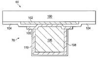
- FIG. 5illustrates a portion of flip chip 60 with a core pillar interconnect structure 78 formed on silicon substrate 100 .
- Flip chip 60has many input/output (I/O) terminals for routing electrical signals and requires a high-density interconnect array containing a large number of core pillar interconnect structures like 78 , similar to FIG. 4 .
- Each core pillar interconnect structure 78provides one I/O terminal.
- the core pillar interconnect structuresneed a fine pitch to minimize its area and maximize the density of the interconnect array.
- FIG. 6describes the process of forming the core pillar interconnect structure 78 .
- the incoming waferundergoes cleaning.
- a metal contact pad 102is formed on substrate 100 by sputtering or other suitable metal deposition process.
- Contact pad 102is made of aluminum (Al), copper (Cu), or aluminum/copper alloys.
- Contact pad 102is electrically connected to active and passive devices through conduction tracks or layers formed on substrate 100 .
- An insulating layer 104is formed over substrate 100 and contact pad 102 .
- the insulating layer 104can be made with SiN, SiO2, SiON, polyimide, BCB, PBO, or other insulating material. A portion of insulating layer 104 is removed by an etching process to expose contact pad 102 .
- UBM 105is deposited and patterned to electrically connect to contact pad 102 .
- UBM 105may include a wetting layer, barrier layer, and adhesive layer.
- the adhesion layeris formed over insulating layer 104 for bonding to the barrier layer.
- the adhesion layercan be titanium (Ti), Al, titanium tungsten (TiW), and chromium (Cr).
- the barrier layerinhibits the diffusion of Cu into the active area of the die.
- the barrier layercan be made of nickel (Ni), Ni-alloy, platinum (Pt), palladium (Pd), TiW, and chromium copper (CrCu).
- the seed layeris formed over the barrier layer.
- the seed layercan be made with Cu, Ni, nickel vanadium (NiV), Cu, gold (Au), or Al.
- the seed layerfollows the contour of insulating layer 104 and contact pad 102 and acts as an intermediate conductive layer formed between metal contact pad 102 and the core pillar.
- a photoresist layer 112is coated, exposed, developed, and etched to form an opening or column having a width which is less than that of contact pad 102 and UBM 105 .
- the opening in photoresist 112is located central to contact pad 102 and UBM 105 , as shown in FIG. 7 .
- an inner core pillar 106is deposited into the opening between photoresist layers 112 by an electroless plating or electrolytic plating process. Core pillar 106 electrically connects to UBM 105 and contact pad 102 .
- Core pillar 106is made with Ni or other similar or suitable metal. Ni pillar plating is a simpler and lower cost process than the Cu pillar and solder plating of prior art step 38 in FIG. 2 .
- photoresist layer 112is removed.
- a metal layer 108is formed over core pillar 106 .
- Metal layer 108is deposited by an electroless plating or electrolytic plating process.
- Metal layer 108is made with Cu or other similar or suitable metal.
- An organic solderability preservative (OSP) 110is coated over metal layer 108 by dipping in an immersion tank.
- the OSPis formed by a series of processing steps including acidic cleaning of the underlying Cu layer 108 , water rinse, micro-etch, water rinse, acid clean, water rinse, air knife, apply OSP, air knife, low pressure water rinse, and drying to expel moisture from the OSP coating and stabilize the materials.
- the micro-etchcan use a hydrogen-peroxide sulfuric acid.
- the Cu metal layer 108maintains a uniform and continuous OSP coating which completely fills the underlying surface.
- the immersion timeis typically less than one minute at a temperature range of 40-45° C.
- the pH of the operating OSP solutionshould be maintained between 4.3 and 4.5.
- the OSP solutionmay contain benzotriazole, rosin, rosin esters, or benzimidazole compounds, as described in U.S. Pat. No. 5,173,130 and incorporated herein by reference.
- a typical benzimidazole compoundmay have an alkyl group of at least three carbon atoms at the 2-position dissolved in an organic acid.
- the benzimidazole compound in an organic acidis converted to a copper complex.
- the copper complexreacts with the bare copper surface and forms a layer of benzimidazole and copper complex.
- the OSP coatingcan also be made with phenylimidazole or other imidazole compounds including 2-arylimidazole as the active ingredient, as described in U.S. Pat. No. 5,560,785 and incorporated herein by reference.
- the OSP coating 110is made about 0.35 micrometers ( ⁇ m) in thickness. The OSP coating 110 selectively protects the bare copper from oxidation, which if allowed to form could interfere with the solderability of the core pillar surface.
- FIG. 8shows metal layer 108 plated over core pillar 106 and coated with OSP 110 .
- core pillar 106has been formed without deposition of solder material or reflow process.
- the absence of solder material deposition and reflowdecreases the pitch of the core pillars and increases I/O density of the interconnect structure.
- the CU layer 108 and OSP coating 110provides good solderability for core pillar 106 to the chip carrier substrate.
- a chip carrier substrate 120has contact pads or UBM 122 formed on its surface.
- the contact pad 122can be Al, Cu, tin (Sn), Ni, Au, or silver (Ag).
- An insulating layer 126is formed over substrate 120 and contact pads 122 . A portion of insulating layer 126 is removed by an etching process to expose contact pads 122 .
- An electrically conductive solder materialis deposited in the insulating layer opening over contact pads 122 using an evaporation, electrolytic plating, electroless plating, ball drop, or screen printing process.
- the solder materialcan be any metal or electrically conductive material, e.g., Sn, lead (Pb), Ni, Au, Ag, Cu, bismuthinite (Bi), and alloys thereof.
- the solder materialcan be eutectic Sn/Pb, high lead, lead free, or other solder materials.
- the solder materialis reflowed by heating the solder material above its melting point to form solder bumps 128 . In some applications, solder bumps 128 are reflowed a second time to improve electrical contact to contact pads 122 .
- the interconnect structure 78 of substrate 100with Cu layer 108 and OSP coating 110 formed over core pillars 106 , is brought into physical contact with solder bumps 128 on carrier substrate 120 .
- the solder bumps 128are reflowed to metallurgically and electrically connect core pillar 106 to the solder bumps, as shown in FIG. 10 .
- the Cu layer 108 and OSP coating 110provides good solderability characteristics while maintaining a fine core pillar pitch.
- the Ni core pillar with Cu outer layer and OSP coatingis used to decrease the pitch between the core pillars in the interconnect array.
- the pitchis smaller in part because the process requires no deposition of solder material or solder reflow process to form the core pillars.
- the decrease in core pillar pitchincreases the number of I/O contacts per unit area on the semiconductor device.
- the density of the interconnect arraycan be increased by about 15%.
Landscapes
- Engineering & Computer Science (AREA)
- Computer Hardware Design (AREA)
- Microelectronics & Electronic Packaging (AREA)
- Power Engineering (AREA)
- Manufacturing & Machinery (AREA)
- Chemical & Material Sciences (AREA)
- Materials Engineering (AREA)
- Mechanical Engineering (AREA)
- Metallurgy (AREA)
- Organic Chemistry (AREA)
- Internal Circuitry In Semiconductor Integrated Circuit Devices (AREA)
Abstract
Description
- The present invention relates in general to semiconductor devices and, more particularly, to a semiconductor device having a high-density interconnect array formed with core pillars having coating of organic solderability preservative to produce a finer pitch and high-density I/O by avoiding solder reflow.
- Semiconductor devices are found in many products in the fields of entertainment, communications, networks, computers, and household markets. Semiconductor devices are also found in military, aviation, automotive, industrial controllers, and office equipment. The semiconductor devices perform a variety of electrical functions necessary for each of these applications.
- The manufacture of semiconductor devices involves formation of a wafer having a plurality of die. Each semiconductor die contains hundreds or thousands of transistors and other active and passive devices performing a variety of electrical functions. For a given wafer, each die from the wafer typically performs the same electrical function. Front-end manufacturing generally refers to formation of the semiconductor devices on the wafer. The finished wafer has an active side containing the transistors and other active and passive components. Back-end manufacturing refers to cutting or singulating the finished wafer into the individual die and then packaging the die for structural support and environmental isolation.
- One goal of semiconductor manufacturing is to produce a package suitable for faster, reliable, smaller, and higher-density integrated circuits (IC) at lower cost. Flip chip packages or wafer level packages (WLP) are ideally suited for ICs demanding high speed, high density, and greater pin count. Flip chip style packaging involves mounting the active side of the die facedown toward a chip carrier substrate or printed circuit board (PCB). The electrical and mechanical interconnect between the active devices on the die and conduction tracks on the carrier substrate is achieved through a solder bump structure comprising a large number of conductive solder bumps or balls. The solder bumps are formed by a reflow process applied to solder material deposited on metal contact pads which are disposed on the semiconductor substrate. The solder bumps are then soldered to the carrier substrate. The flip chip semiconductor package provides a short electrical conduction path from the active devices on the die to the carrier substrate in order to reduce signal propagation, lower capacitance, and achieve overall better circuit performance.
FIG. 1 illustrates a portion of aconventional flip chip 10 with a core pillar andsolder bump 11 formed onsilicon substrate 12.FIG. 2 describes the process of forming the core pillar andsolder bump 11. Instep 30, the incoming wafer undergoes cleaning. Instep 32,metal contact pad 14 is formed onsubstrate 12 by sputtering.Contact pad 14 is made of aluminum, copper, or aluminum/copper alloys.Contact pad 14 is electrically connected to active and passive devices through conduction tracks or layers formed onsubstrate 12. Aninsulating layer 16 is formed oversubstrate 12 andcontact pad 14. Theinsulating layer 16 can be made with silicon nitride (SiN), silicon dioxide (SiO2), silicon oxynitride (SiON), polyimide, benzocyclobutene (BCB), polybenzoxazole (PBO), or other insulating material. A portion ofinsulating layer 16 is removed by an etching process to exposemetal contact pad 14. An under bump metallization (UBM)18 is deposited and patterned to electrically connect tocontact pad 14. In one embodiment,UBMs 18 may include a wetting layer, barrier layer, and adhesive layer.- In
steps FIG. 2 , aphotoresist layer 54 is coated, exposed, developed, and etched to form a first opening or column having a width which is less than that ofcontact pad 14 and UBM18. The first opening is located central to contactpad 14 and UBM18, as shown inFIG. 3 . Instep 38, aninner core pillar 20 is plated into the first opening betweenphotoresist layers 54.Core pillar 20 electrically connects to UBM18 andcontact pad 14.Core pillar 20 is made of Cu. An electrically conductive solder material is deposited overpillar 20 through an evaporation, electrolytic plating, electroless plating, ball drop, or screen printing process. The solder material can be any metal or electrically conductive material, e.g., Sn, Pb, Ni, Au, Ag, Cu, Bi, and alloys thereof. Instep 40,photoresist layer 54 is removed. Instep 42, the solder material is reflowed by heating the solder material above its melting point to formsolder bumps 22 oncore pillars 20, as seen in the final structure ofFIG. 1 . - Many interconnect structures for flip chips use a version of the above-described core pillar and solder bumps in an interconnect array. The core pillar and solder bumps are common in high-density arrays having many input/output (I/O) terminals for routing electrical signals. The core pillar and solder bump structures require solder deposition and solder reflow to preserve the insulating layer. The solder deposition and reflow processes limit the density of the core pillars and solder bumps that can be formed per unit area in the interconnect array.
- A need exists for high-density interconnect structures without solder deposition or solder reflow to form the core pillars.
- In one embodiment, the present invention is a method of making an interconnect structure on a semiconductor device comprising the steps of providing a substrate, forming a contact pad on the substrate, forming an under bump metallization layer over the contact pad, forming a photoresist layer over the substrate, removing a portion of the photoresist layer to form an opening which exposes the under bump metallization layer, depositing a first conductive material into the opening of the photoresist, removing the photoresist layer, depositing a second conductive material over the first conductive material, and coating the second conductive material with an organic solderability preservative.
- In another embodiment, the present invention is a method of making an interconnect structure on a semiconductor device comprising the steps of providing a substrate, forming a contact pad on the substrate, forming a core pillar over the contact pad, the core pillar being made with a first conductive material, depositing a second conductive material over the core pillar, and coating the second conductive material with an organic solderability preservative.
- In another embodiment, the present invention is a method of making an interconnect structure on a semiconductor device comprising the steps of providing a substrate, forming an under bump metallization layer over the substrate, forming a photoresist layer having an opening over the under bump metallization layer, plating a first conductive material into the opening of the photoresist layer to form a core pillar, plating a second conductive material over the core pillar, and coating the second conductive material with an organic solderability preservative.
- In another embodiment, the present invention is a semiconductor device having an interconnect structure comprising a substrate and a contact pad formed on the substrate. A core pillar is formed over the contact pad. The core pillar is made with a first conductive material. A second conductive material is deposited over the core pillar. An organic solderability preservative coats the second conductive material.
FIG. 1 is a conventional core pillar and solder bump formed on a contact pad of a flip chip;FIG. 2 is a known process for forming the core pillar and solder bump;FIG. 3 illustrates conventional deposition of metal and solder material into photoresist opening to form the core pillar and solder bump;FIG. 4 is a flip chip semiconductor device with solder bumps providing electrical interconnect between an active area of the die and a chip carrier substrate;FIG. 5 illustrates a core pillar interconnect structure for a high-density interconnect array coated with organic solderability preservative;FIG. 6 is a process for forming the core pillar in the high-density interconnect array using an OSP coating;FIG. 7 illustrates deposition of a first metal into photoresist openings to form the core pillar;FIG. 8 illustrates deposition of a second metal layer and OSP coating over the core pillar;FIG. 9 shows the core pillars coated with OSP in physical contact with solder bumps on a carrier substrate; andFIG. 10 illustrates reflow of carrier substrate solder bumps to metallurgically connect to the core pillars.- The present invention is described in one or more embodiments in the following description with reference to the Figures, in which like numerals represent the same or similar elements. While the invention is described in terms of the best mode for achieving the invention's objectives, it will be appreciated by those skilled in the art that it is intended to cover alternatives, modifications, and equivalents as may be included within the spirit and scope of the invention as defined by the appended claims and their equivalents as supported by the following disclosure and drawings.
- The manufacture of semiconductor devices involves formation of a wafer having a plurality of die. Each die contains hundreds or thousands of transistors and other active and passive devices performing one or more electrical functions. For a given wafer, each die from the wafer typically performs the same electrical function. Front-end manufacturing generally refers to formation of the semiconductor devices on the wafer. The finished wafer has an active side containing the transistors and other active and passive components. Back-end manufacturing refers to cutting or singulating the finished wafer into the individual die and then packaging the die for structural support and/or environmental isolation.
- A semiconductor wafer generally includes an active surface having semiconductor devices disposed thereon, and a backside surface formed with bulk semiconductor material, e.g., silicon. The active side surface contains a plurality of semiconductor die. The active surface is formed by a variety of semiconductor processes, including layering, patterning, doping, and heat treatment. In the layering process, semiconductor materials are grown or deposited on the substrate by techniques involving thermal oxidation, nitridation, chemical vapor deposition, evaporation, and sputtering. Photolithography involves the masking of areas of the surface and etching away undesired material to form specific structures. The doping process injects concentrations of dopant material by thermal diffusion or ion implantation.
- Flip chip semiconductor packages and wafer level packages (WLP) are commonly used with integrated circuits (ICs) demanding high speed, high density, and greater pin count. Flip chip
style semiconductor device 60 involves mounting anactive area 62 ofdie 64 facedown toward a chip carrier substrate or printed circuit board (PCB)66, as shown inFIG. 4 .Active area 62 contains active and passive devices, conductive layers, and dielectric layers according to the electrical design of the die. The electrical and mechanical interconnect is achieved through asolder bump structure 70 comprising a large number of individual conductive solder bumps orballs 72. The solder bumps are formed on bump pads orinterconnect sites 74, which are disposed onactive area 62. Thebump pads 74 connect to the active circuits by conduction tracks inactive area 62. The solder bumps72 are electrically and mechanically connected to contact pads orinterconnect sites 76 oncarrier substrate 66. The flip chip semiconductor device provides a short electrical conduction path from the active devices on die64 to conduction tracks oncarrier substrate 66 in order to reduce signal propagation, lower capacitance, and achieve overall better circuit performance. FIG. 5 illustrates a portion offlip chip 60 with a corepillar interconnect structure 78 formed onsilicon substrate 100.Flip chip 60 has many input/output (I/O) terminals for routing electrical signals and requires a high-density interconnect array containing a large number of core pillar interconnect structures like78, similar toFIG. 4 . Each corepillar interconnect structure 78 provides one I/O terminal. The core pillar interconnect structures need a fine pitch to minimize its area and maximize the density of the interconnect array.FIG. 6 describes the process of forming the corepillar interconnect structure 78. Instep 80, the incoming wafer undergoes cleaning. Instep 82, ametal contact pad 102 is formed onsubstrate 100 by sputtering or other suitable metal deposition process.Contact pad 102 is made of aluminum (Al), copper (Cu), or aluminum/copper alloys.Contact pad 102 is electrically connected to active and passive devices through conduction tracks or layers formed onsubstrate 100. An insulatinglayer 104 is formed oversubstrate 100 andcontact pad 102. The insulatinglayer 104 can be made with SiN, SiO2, SiON, polyimide, BCB, PBO, or other insulating material. A portion of insulatinglayer 104 is removed by an etching process to exposecontact pad 102.- An under bump metallization layer (UBM)105 is deposited and patterned to electrically connect to contact
pad 102. In one embodiment,UBM 105 may include a wetting layer, barrier layer, and adhesive layer. The adhesion layer is formed overinsulating layer 104 for bonding to the barrier layer. The adhesion layer can be titanium (Ti), Al, titanium tungsten (TiW), and chromium (Cr). The barrier layer inhibits the diffusion of Cu into the active area of the die. The barrier layer can be made of nickel (Ni), Ni-alloy, platinum (Pt), palladium (Pd), TiW, and chromium copper (CrCu). The seed layer is formed over the barrier layer. The seed layer can be made with Cu, Ni, nickel vanadium (NiV), Cu, gold (Au), or Al. The seed layer follows the contour of insulatinglayer 104 andcontact pad 102 and acts as an intermediate conductive layer formed betweenmetal contact pad 102 and the core pillar. - In
steps FIG. 6 , a photoresist layer112 is coated, exposed, developed, and etched to form an opening or column having a width which is less than that ofcontact pad 102 andUBM 105. The opening in photoresist112 is located central tocontact pad 102 andUBM 105, as shown inFIG. 7 . Instep 88, aninner core pillar 106 is deposited into the opening between photoresist layers112 by an electroless plating or electrolytic plating process.Core pillar 106 electrically connects toUBM 105 andcontact pad 102.Core pillar 106 is made with Ni or other similar or suitable metal. Ni pillar plating is a simpler and lower cost process than the Cu pillar and solder plating ofprior art step 38 inFIG. 2 . Instep 90, photoresist layer112 is removed. - In
step 92 ofFIG. 6 , ametal layer 108 is formed overcore pillar 106.Metal layer 108 is deposited by an electroless plating or electrolytic plating process.Metal layer 108 is made with Cu or other similar or suitable metal. An organic solderability preservative (OSP)110 is coated overmetal layer 108 by dipping in an immersion tank. - In one embodiment, the OSP is formed by a series of processing steps including acidic cleaning of the
underlying Cu layer 108, water rinse, micro-etch, water rinse, acid clean, water rinse, air knife, apply OSP, air knife, low pressure water rinse, and drying to expel moisture from the OSP coating and stabilize the materials. The micro-etch can use a hydrogen-peroxide sulfuric acid. TheCu metal layer 108 maintains a uniform and continuous OSP coating which completely fills the underlying surface. The immersion time is typically less than one minute at a temperature range of 40-45° C. The pH of the operating OSP solution should be maintained between 4.3 and 4.5. The OSP solution may contain benzotriazole, rosin, rosin esters, or benzimidazole compounds, as described in U.S. Pat. No. 5,173,130 and incorporated herein by reference. A typical benzimidazole compound may have an alkyl group of at least three carbon atoms at the 2-position dissolved in an organic acid. When the bare copper surface is immersed in OSP solution, the benzimidazole compound in an organic acid is converted to a copper complex. The copper complex reacts with the bare copper surface and forms a layer of benzimidazole and copper complex. By incorporating copper ions in the aqueous solution of the benzimidazole and acid, the reaction rate is enhanced. - Alternatively, the OSP coating can also be made with phenylimidazole or other imidazole compounds including 2-arylimidazole as the active ingredient, as described in U.S. Pat. No. 5,560,785 and incorporated herein by reference. In any case, the
OSP coating 110 is made about 0.35 micrometers (μm) in thickness. TheOSP coating 110 selectively protects the bare copper from oxidation, which if allowed to form could interfere with the solderability of the core pillar surface.FIG. 8 showsmetal layer 108 plated overcore pillar 106 and coated withOSP 110. - Note that
core pillar 106 has been formed without deposition of solder material or reflow process. The absence of solder material deposition and reflow decreases the pitch of the core pillars and increases I/O density of the interconnect structure. TheCU layer 108 andOSP coating 110 provides good solderability forcore pillar 106 to the chip carrier substrate. - In
FIG. 9 , achip carrier substrate 120 has contact pads orUBM 122 formed on its surface. Thecontact pad 122 can be Al, Cu, tin (Sn), Ni, Au, or silver (Ag). An insulatinglayer 126 is formed oversubstrate 120 andcontact pads 122. A portion of insulatinglayer 126 is removed by an etching process to exposecontact pads 122. An electrically conductive solder material is deposited in the insulating layer opening overcontact pads 122 using an evaporation, electrolytic plating, electroless plating, ball drop, or screen printing process. The solder material can be any metal or electrically conductive material, e.g., Sn, lead (Pb), Ni, Au, Ag, Cu, bismuthinite (Bi), and alloys thereof. For example, the solder material can be eutectic Sn/Pb, high lead, lead free, or other solder materials. The solder material is reflowed by heating the solder material above its melting point to form solder bumps128. In some applications, solder bumps128 are reflowed a second time to improve electrical contact to contactpads 122. - The
interconnect structure 78 ofsubstrate 100, withCu layer 108 andOSP coating 110 formed overcore pillars 106, is brought into physical contact withsolder bumps 128 oncarrier substrate 120. The solder bumps128 are reflowed to metallurgically and electrically connectcore pillar 106 to the solder bumps, as shown inFIG. 10 . TheCu layer 108 andOSP coating 110 provides good solderability characteristics while maintaining a fine core pillar pitch. - In summary, flip chips requiring a high-density interconnect array have many I/O terminals for routing electrical signals to external devices. The Ni core pillar with Cu outer layer and OSP coating, such as shown in
FIG. 5 , is used to decrease the pitch between the core pillars in the interconnect array. The pitch is smaller in part because the process requires no deposition of solder material or solder reflow process to form the core pillars. The decrease in core pillar pitch increases the number of I/O contacts per unit area on the semiconductor device. The density of the interconnect array can be increased by about 15%. - While one or more embodiments of the present invention have been illustrated in detail, the skilled artisan will appreciate that modifications and adaptations to those embodiments may be made without departing from the scope of the present invention as set forth in the following claims.
Claims (25)
Priority Applications (2)
| Application Number | Priority Date | Filing Date | Title |
|---|---|---|---|
| US12/046,761US20090233436A1 (en) | 2008-03-12 | 2008-03-12 | Semiconductor Device Having High-Density Interconnect Array with Core Pillars Formed With OSP Coating |
| US14/181,429US20140159236A1 (en) | 2008-03-12 | 2014-02-14 | Semiconductor Device Having High-Density Interconnect Array with Core Pillars Formed With OSP Coating |
Applications Claiming Priority (1)
| Application Number | Priority Date | Filing Date | Title |
|---|---|---|---|
| US12/046,761US20090233436A1 (en) | 2008-03-12 | 2008-03-12 | Semiconductor Device Having High-Density Interconnect Array with Core Pillars Formed With OSP Coating |
Related Child Applications (1)
| Application Number | Title | Priority Date | Filing Date |
|---|---|---|---|
| US14/181,429ContinuationUS20140159236A1 (en) | 2008-03-12 | 2014-02-14 | Semiconductor Device Having High-Density Interconnect Array with Core Pillars Formed With OSP Coating |
Publications (1)
| Publication Number | Publication Date |
|---|---|
| US20090233436A1true US20090233436A1 (en) | 2009-09-17 |
Family
ID=41063500
Family Applications (2)
| Application Number | Title | Priority Date | Filing Date |
|---|---|---|---|
| US12/046,761AbandonedUS20090233436A1 (en) | 2008-03-12 | 2008-03-12 | Semiconductor Device Having High-Density Interconnect Array with Core Pillars Formed With OSP Coating |
| US14/181,429AbandonedUS20140159236A1 (en) | 2008-03-12 | 2014-02-14 | Semiconductor Device Having High-Density Interconnect Array with Core Pillars Formed With OSP Coating |
Family Applications After (1)
| Application Number | Title | Priority Date | Filing Date |
|---|---|---|---|
| US14/181,429AbandonedUS20140159236A1 (en) | 2008-03-12 | 2014-02-14 | Semiconductor Device Having High-Density Interconnect Array with Core Pillars Formed With OSP Coating |
Country Status (1)
| Country | Link |
|---|---|
| US (2) | US20090233436A1 (en) |
Cited By (42)
| Publication number | Priority date | Publication date | Assignee | Title |
|---|---|---|---|---|
| US20100252311A1 (en)* | 2009-04-01 | 2010-10-07 | Advanced Interconnections Corp. | Terminal assembly with regions of differing solderability |
| CN102201375A (en)* | 2010-03-24 | 2011-09-28 | 台湾积体电路制造股份有限公司 | Integrated circuit device and packaging assembly |
| US8232193B2 (en) | 2010-07-08 | 2012-07-31 | Taiwan Semiconductor Manufacturing Company, Ltd. | Method of forming Cu pillar capped by barrier layer |
| US20120295434A1 (en)* | 2011-05-18 | 2012-11-22 | Samsung Electronics Co., Ltd | Solder collapse free bumping process of semiconductor device |
| US20130093076A1 (en)* | 2011-10-13 | 2013-04-18 | Taiwan Semiconductor Manufacturing Company, Ltd. | Semiconductor package and method of forming the same |
| US8435881B2 (en) | 2011-06-23 | 2013-05-07 | STAT ChipPAC, Ltd. | Semiconductor device and method of forming protective coating over interconnect structure to inhibit surface oxidation |
| US8492891B2 (en) | 2010-04-22 | 2013-07-23 | Taiwan Semiconductor Manufacturing Company, Ltd. | Cu pillar bump with electrolytic metal sidewall protection |
| US20130234311A1 (en)* | 2009-09-29 | 2013-09-12 | Semiconductor Components Industries, Llc | Semiconductor component that includes a protective structure |
| WO2013116876A3 (en)* | 2012-02-03 | 2013-11-07 | Avery Dennison Corporation | Sheet assembly with aluminum based electrodes |
| US20130313695A1 (en)* | 2012-05-24 | 2013-11-28 | Nichia Corporation | Semiconductor device |
| CN103915357A (en)* | 2014-04-16 | 2014-07-09 | 华进半导体封装先导技术研发中心有限公司 | Manufacturing method of superfine interval micro protruding point |
| US8803333B2 (en) | 2012-05-18 | 2014-08-12 | Taiwan Semiconductor Manufacturing Company, Ltd. | Three-dimensional chip stack and method of forming the same |
| US8823166B2 (en) | 2010-08-30 | 2014-09-02 | Taiwan Semiconductor Manufacturing Company, Ltd. | Pillar bumps and process for making same |
| US20150021767A1 (en)* | 2013-07-16 | 2015-01-22 | Doo Hyun Park | Semiconductor device with plated conductive pillar coupling |
| US20150027750A1 (en)* | 2012-05-16 | 2015-01-29 | Ngk Spark Plug Co., Ltd. | Wiring board |
| US8970034B2 (en)* | 2012-05-09 | 2015-03-03 | Micron Technology, Inc. | Semiconductor assemblies and structures |
| US8969734B2 (en) | 2009-04-01 | 2015-03-03 | Advanced Interconnections Corp. | Terminal assembly with regions of differing solderability |
| US20150228533A1 (en)* | 2010-06-02 | 2015-08-13 | Taiwan Semiconductor Manufacturing Company, Ltd. | Method of forming cu pillar bump with non-metal sidewall spacer and metal top cap |
| US20150262953A1 (en)* | 2014-03-13 | 2015-09-17 | Taiwan Semiconductor Manufacturing Co., Ltd | Semiconductor device structure and manufacturing method |
| CN104981092A (en)* | 2015-06-17 | 2015-10-14 | 三星半导体(中国)研究开发有限公司 | Surface plating and semiconductor package including the surface plating |
| JP2015216344A (en)* | 2014-04-21 | 2015-12-03 | 新光電気工業株式会社 | Wiring board and method of manufacturing the same |
| US20160013162A1 (en)* | 2010-05-20 | 2016-01-14 | Taiwan Semiconductor Manufacturing Company, Ltd. | Substrate Interconnections having Different Sizes |
| US20160372408A1 (en)* | 2015-06-17 | 2016-12-22 | Samsung Electronics Co., Ltd. | Methods of manufacturing printed circuit board and semiconductor package |
| US20170098627A1 (en)* | 2014-04-23 | 2017-04-06 | Massachusetts Institute Of Technology | Interconnect structures for fine pitch assembly of semiconductor structures |
| TWI595576B (en)* | 2014-05-23 | 2017-08-11 | 艾馬克科技公司 | Copper pillar sidewall protection |
| US9780075B2 (en) | 2014-08-11 | 2017-10-03 | Massachusetts Institute Of Technology | Interconnect structures for assembly of multi-layer semiconductor devices |
| US9812429B2 (en) | 2014-11-05 | 2017-11-07 | Massachusetts Institute Of Technology | Interconnect structures for assembly of multi-layer semiconductor devices |
| US9953939B2 (en) | 2012-09-18 | 2018-04-24 | Taiwan Semiconductor Manufacturing Company, Ltd. | Conductive contacts having varying widths and method of manufacturing same |
| US9991224B2 (en) | 2012-04-18 | 2018-06-05 | Taiwan Semiconductor Manufacturing Company, Ltd. | Bump-on-trace interconnect having varying widths and methods of forming same |
| US10056345B2 (en) | 2012-04-17 | 2018-08-21 | Taiwan Semiconductor Manufacturing Company, Ltd. | Conical-shaped or tier-shaped pillar connections |
| US10121754B2 (en) | 2015-11-05 | 2018-11-06 | Massachusetts Institute Of Technology | Interconnect structures and methods for fabricating interconnect structures |
| US10134972B2 (en) | 2015-07-23 | 2018-11-20 | Massachusetts Institute Of Technology | Qubit and coupler circuit structures and coupling techniques |
| TWI647807B (en)* | 2017-01-24 | 2019-01-11 | 旺宏電子股份有限公司 | Interconnect structure and fabricating method thereof |
| US10204851B2 (en)* | 2011-12-31 | 2019-02-12 | Intel Corporation | High density package interconnects |
| US10204859B2 (en)* | 2017-01-25 | 2019-02-12 | Macronix International Co., Ltd. | Interconnect structure and fabricating method thereof |
| US10242968B2 (en) | 2015-11-05 | 2019-03-26 | Massachusetts Institute Of Technology | Interconnect structure and semiconductor structures for assembly of cryogenic electronic packages |
| US10381541B2 (en) | 2016-10-11 | 2019-08-13 | Massachusetts Institute Of Technology | Cryogenic electronic packages and methods for fabricating cryogenic electronic packages |
| US10658424B2 (en) | 2015-07-23 | 2020-05-19 | Massachusetts Institute Of Technology | Superconducting integrated circuit |
| US20200258800A1 (en)* | 2019-02-12 | 2020-08-13 | Intel Corporation | Subtractive etch resolution implementing a functional thin metal resist |
| US11462520B2 (en)* | 2014-07-29 | 2022-10-04 | Huawei Technologies Co., Ltd. | Chip integration module, chip package structure, and chip integration method |
| US11553599B2 (en)* | 2018-12-24 | 2023-01-10 | AT&S(Chongqing) Company Limited | Component carrier comprising pillars on a coreless substrate |
| US11616007B2 (en)* | 2020-10-08 | 2023-03-28 | Advanced Semiconductor Engineering, Inc. | Electronic package |
Families Citing this family (4)
| Publication number | Priority date | Publication date | Assignee | Title |
|---|---|---|---|---|
| CN104509231A (en)* | 2012-07-28 | 2015-04-08 | 莱尔德技术股份有限公司 | Metallized film-over-foam contacts |
| WO2016019335A1 (en)* | 2014-08-01 | 2016-02-04 | Kyocera America, Inc. | Chip attachment system |
| US9806052B2 (en)* | 2015-09-15 | 2017-10-31 | Qualcomm Incorporated | Semiconductor package interconnect |
| JP7251951B2 (en)* | 2018-11-13 | 2023-04-04 | 新光電気工業株式会社 | Semiconductor device and method for manufacturing semiconductor device |
Citations (6)
| Publication number | Priority date | Publication date | Assignee | Title |
|---|---|---|---|---|
| US5858074A (en)* | 1997-07-29 | 1999-01-12 | National Research Council Of Canada | Organic solderability preservative compositions |
| US20020173073A1 (en)* | 2001-05-16 | 2002-11-21 | Industrial Technology Research Institute | Fabricating process for forming multi-layered metal bumps by electroless plating |
| US6495397B2 (en)* | 2001-03-28 | 2002-12-17 | Intel Corporation | Fluxless flip chip interconnection |
| US6524644B1 (en)* | 1999-08-26 | 2003-02-25 | Enthone Inc. | Process for selective deposition of OSP coating on copper, excluding deposition on gold |
| US20050173809A1 (en)* | 2004-01-22 | 2005-08-11 | Yukihiro Yamamoto | Wafer-level package and method for production thereof |
| US20060094223A1 (en)* | 2004-11-03 | 2006-05-04 | Advanced Semiconductor Engineering, Inc. | Fabrication method of a wafer structure |
Family Cites Families (6)
| Publication number | Priority date | Publication date | Assignee | Title |
|---|---|---|---|---|
| US5011711A (en)* | 1989-07-18 | 1991-04-30 | Toyo Kohan Co., Ltd. | Method for post-treatment of electroplated steel sheets for soldering |
| US6204454B1 (en)* | 1997-12-27 | 2001-03-20 | Tdk Corporation | Wiring board and process for the production thereof |
| JP3968554B2 (en)* | 2000-05-01 | 2007-08-29 | セイコーエプソン株式会社 | Bump forming method and semiconductor device manufacturing method |
| US7794531B2 (en)* | 2007-01-08 | 2010-09-14 | Enthone Inc. | Organic solderability preservative comprising high boiling temperature alcohol |
| JP5629580B2 (en)* | 2007-09-28 | 2014-11-19 | テッセラ,インコーポレイテッド | Flip chip interconnect with double posts |
| US7993971B2 (en)* | 2007-12-28 | 2011-08-09 | Freescale Semiconductor, Inc. | Forming a 3-D semiconductor die structure with an intermetallic formation |
- 2008
- 2008-03-12USUS12/046,761patent/US20090233436A1/ennot_activeAbandoned
- 2014
- 2014-02-14USUS14/181,429patent/US20140159236A1/ennot_activeAbandoned
Patent Citations (6)
| Publication number | Priority date | Publication date | Assignee | Title |
|---|---|---|---|---|
| US5858074A (en)* | 1997-07-29 | 1999-01-12 | National Research Council Of Canada | Organic solderability preservative compositions |
| US6524644B1 (en)* | 1999-08-26 | 2003-02-25 | Enthone Inc. | Process for selective deposition of OSP coating on copper, excluding deposition on gold |
| US6495397B2 (en)* | 2001-03-28 | 2002-12-17 | Intel Corporation | Fluxless flip chip interconnection |
| US20020173073A1 (en)* | 2001-05-16 | 2002-11-21 | Industrial Technology Research Institute | Fabricating process for forming multi-layered metal bumps by electroless plating |
| US20050173809A1 (en)* | 2004-01-22 | 2005-08-11 | Yukihiro Yamamoto | Wafer-level package and method for production thereof |
| US20060094223A1 (en)* | 2004-11-03 | 2006-05-04 | Advanced Semiconductor Engineering, Inc. | Fabrication method of a wafer structure |
Cited By (86)
| Publication number | Priority date | Publication date | Assignee | Title |
|---|---|---|---|---|
| US20100252311A1 (en)* | 2009-04-01 | 2010-10-07 | Advanced Interconnections Corp. | Terminal assembly with regions of differing solderability |
| US8119926B2 (en)* | 2009-04-01 | 2012-02-21 | Advanced Interconnections Corp. | Terminal assembly with regions of differing solderability |
| US8969734B2 (en) | 2009-04-01 | 2015-03-03 | Advanced Interconnections Corp. | Terminal assembly with regions of differing solderability |
| US9263390B2 (en)* | 2009-09-29 | 2016-02-16 | Semiconductor Components Industries, Llc | Semiconductor component that includes a protective structure |
| US20130234311A1 (en)* | 2009-09-29 | 2013-09-12 | Semiconductor Components Industries, Llc | Semiconductor component that includes a protective structure |
| CN102201375A (en)* | 2010-03-24 | 2011-09-28 | 台湾积体电路制造股份有限公司 | Integrated circuit device and packaging assembly |
| US9006097B2 (en) | 2010-04-22 | 2015-04-14 | Taiwan Semiconductor Manufacturing Company, Ltd. | Cu pillar bump with electrolytic metal sidewall protection |
| US8492891B2 (en) | 2010-04-22 | 2013-07-23 | Taiwan Semiconductor Manufacturing Company, Ltd. | Cu pillar bump with electrolytic metal sidewall protection |
| US20160013162A1 (en)* | 2010-05-20 | 2016-01-14 | Taiwan Semiconductor Manufacturing Company, Ltd. | Substrate Interconnections having Different Sizes |
| US9773755B2 (en)* | 2010-05-20 | 2017-09-26 | Taiwan Semiconductor Manufacturing Company, Ltd. | Substrate interconnections having different sizes |
| US20150228533A1 (en)* | 2010-06-02 | 2015-08-13 | Taiwan Semiconductor Manufacturing Company, Ltd. | Method of forming cu pillar bump with non-metal sidewall spacer and metal top cap |
| US9685372B2 (en)* | 2010-06-02 | 2017-06-20 | Taiwan Semiconductor Manufacturing Company, Ltd. | Method of forming Cu pillar bump with non-metal sidewall spacer and metal top cap |
| US8653659B2 (en) | 2010-07-08 | 2014-02-18 | Taiwan Semiconductor Manufacturing Company, Ltd. | Integrated circuit device including a copper pillar capped by barrier layer |
| US8232193B2 (en) | 2010-07-08 | 2012-07-31 | Taiwan Semiconductor Manufacturing Company, Ltd. | Method of forming Cu pillar capped by barrier layer |
| US9627339B2 (en) | 2010-07-08 | 2017-04-18 | Taiwan Semiconductor Manufacturing Company, Ltd. | Method of forming an integrated circuit device including a pillar capped by barrier layer |
| US9142521B2 (en) | 2010-07-08 | 2015-09-22 | Taiwan Semiconductor Manufacturing Company, Ltd. | Integrated circuit device including a copper pillar capped by barrier layer and method of forming the same |
| US8823166B2 (en) | 2010-08-30 | 2014-09-02 | Taiwan Semiconductor Manufacturing Company, Ltd. | Pillar bumps and process for making same |
| US9449931B2 (en) | 2010-08-30 | 2016-09-20 | Taiwan Semiconductor Manufacturing Company, Ltd. | Pillar bumps and process for making same |
| US20120295434A1 (en)* | 2011-05-18 | 2012-11-22 | Samsung Electronics Co., Ltd | Solder collapse free bumping process of semiconductor device |
| US8980739B2 (en)* | 2011-05-18 | 2015-03-17 | Samsung Electronics Co., Ltd. | Solder collapse free bumping process of semiconductor device |
| US8912650B2 (en) | 2011-06-23 | 2014-12-16 | Stats Chippac, Ltd. | Semiconductor device and method of forming protective coating over interconnect structure to inhibit surface oxidation |
| US8435881B2 (en) | 2011-06-23 | 2013-05-07 | STAT ChipPAC, Ltd. | Semiconductor device and method of forming protective coating over interconnect structure to inhibit surface oxidation |
| US9536818B2 (en)* | 2011-10-13 | 2017-01-03 | Taiwan Semiconductor Manufacturing Company, Ltd. | Semiconductor package and method of forming the same |
| US20130093076A1 (en)* | 2011-10-13 | 2013-04-18 | Taiwan Semiconductor Manufacturing Company, Ltd. | Semiconductor package and method of forming the same |
| US10658279B2 (en) | 2011-12-31 | 2020-05-19 | Intel Corporation | High density package interconnects |
| US10204851B2 (en)* | 2011-12-31 | 2019-02-12 | Intel Corporation | High density package interconnects |
| WO2013116876A3 (en)* | 2012-02-03 | 2013-11-07 | Avery Dennison Corporation | Sheet assembly with aluminum based electrodes |
| US11315896B2 (en) | 2012-04-17 | 2022-04-26 | Taiwan Semiconductor Manufacturing Company, Ltd. | Conical-shaped or tier-shaped pillar connections |
| US10056345B2 (en) | 2012-04-17 | 2018-08-21 | Taiwan Semiconductor Manufacturing Company, Ltd. | Conical-shaped or tier-shaped pillar connections |
| US11682651B2 (en) | 2012-04-18 | 2023-06-20 | Taiwan Semiconductor Manufacturing Company | Bump-on-trace interconnect |
| US10510710B2 (en) | 2012-04-18 | 2019-12-17 | Taiwan Semiconductor Manufacturing Company, Ltd. | Bump-on-trace interconnect |
| US9991224B2 (en) | 2012-04-18 | 2018-06-05 | Taiwan Semiconductor Manufacturing Company, Ltd. | Bump-on-trace interconnect having varying widths and methods of forming same |
| US10847493B2 (en) | 2012-04-18 | 2020-11-24 | Taiwan Semiconductor Manufacturing, Ltd. | Bump-on-trace interconnect |
| US9224715B2 (en) | 2012-05-09 | 2015-12-29 | Micron Technology, Inc. | Methods of forming semiconductor die assemblies |
| US8970034B2 (en)* | 2012-05-09 | 2015-03-03 | Micron Technology, Inc. | Semiconductor assemblies and structures |
| US9560739B2 (en)* | 2012-05-16 | 2017-01-31 | Ngk Spark Plug Co., Ltd. | Wiring board |
| US20150027750A1 (en)* | 2012-05-16 | 2015-01-29 | Ngk Spark Plug Co., Ltd. | Wiring board |
| US8803333B2 (en) | 2012-05-18 | 2014-08-12 | Taiwan Semiconductor Manufacturing Company, Ltd. | Three-dimensional chip stack and method of forming the same |
| USRE47708E1 (en)* | 2012-05-24 | 2019-11-05 | Nichia Corporation | Semiconductor device |
| US9117803B2 (en)* | 2012-05-24 | 2015-08-25 | Nichia Corporation | Method for manufacturing a semiconductor device |
| US20140287557A1 (en)* | 2012-05-24 | 2014-09-25 | Nichia Corporation | Semiconductor device |
| US8779567B2 (en)* | 2012-05-24 | 2014-07-15 | Nichia Corporation | Semiconductor device |
| US20130313695A1 (en)* | 2012-05-24 | 2013-11-28 | Nichia Corporation | Semiconductor device |
| US11961810B2 (en) | 2012-09-18 | 2024-04-16 | Taiwan Semiconductor Manufacturing Company | Solderless interconnection structure and method of forming same |
| US11043462B2 (en) | 2012-09-18 | 2021-06-22 | Taiwan Semiconductor Manufacturing Company | Solderless interconnection structure and method of forming same |
| US9953939B2 (en) | 2012-09-18 | 2018-04-24 | Taiwan Semiconductor Manufacturing Company, Ltd. | Conductive contacts having varying widths and method of manufacturing same |
| US9966346B2 (en) | 2012-09-18 | 2018-05-08 | Taiwan Semiconductor Manufacturing Company | Bump structure and method of forming same |
| US10008459B2 (en) | 2012-09-18 | 2018-06-26 | Taiwan Semiconductor Manufacturing Company | Structures having a tapering curved profile and methods of making same |
| US10319691B2 (en) | 2012-09-18 | 2019-06-11 | Taiwan Semiconductor Manufacturing Company | Solderless interconnection structure and method of forming same |
| US20150021767A1 (en)* | 2013-07-16 | 2015-01-22 | Doo Hyun Park | Semiconductor device with plated conductive pillar coupling |
| US9735123B2 (en)* | 2014-03-13 | 2017-08-15 | Taiwan Semiconductor Manufacturing Company, Ltd. | Semiconductor device structure and manufacturing method |
| US20150262953A1 (en)* | 2014-03-13 | 2015-09-17 | Taiwan Semiconductor Manufacturing Co., Ltd | Semiconductor device structure and manufacturing method |
| CN103915357A (en)* | 2014-04-16 | 2014-07-09 | 华进半导体封装先导技术研发中心有限公司 | Manufacturing method of superfine interval micro protruding point |
| JP2015216344A (en)* | 2014-04-21 | 2015-12-03 | 新光電気工業株式会社 | Wiring board and method of manufacturing the same |
| US9786633B2 (en)* | 2014-04-23 | 2017-10-10 | Massachusetts Institute Of Technology | Interconnect structures for fine pitch assembly of semiconductor structures and related techniques |
| US20170098627A1 (en)* | 2014-04-23 | 2017-04-06 | Massachusetts Institute Of Technology | Interconnect structures for fine pitch assembly of semiconductor structures |
| TWI595576B (en)* | 2014-05-23 | 2017-08-11 | 艾馬克科技公司 | Copper pillar sidewall protection |
| KR101905334B1 (en)* | 2014-05-23 | 2018-10-05 | 앰코 테크놀로지 인코포레이티드 | Method for semiconductor packaging and electronic device |
| US9875980B2 (en)* | 2014-05-23 | 2018-01-23 | Amkor Technology, Inc. | Copper pillar sidewall protection |
| US11462520B2 (en)* | 2014-07-29 | 2022-10-04 | Huawei Technologies Co., Ltd. | Chip integration module, chip package structure, and chip integration method |
| US10229897B2 (en) | 2014-08-11 | 2019-03-12 | Massachusetts Institute Of Technology | Multi-layer semiconductor structure and methods for fabricating multi-layer semiconductor structures |
| US10418350B2 (en) | 2014-08-11 | 2019-09-17 | Massachusetts Institute Of Technology | Semiconductor structures for assembly in multi-layer semiconductor devices including at least one semiconductor structure |
| US10079224B2 (en) | 2014-08-11 | 2018-09-18 | Massachusetts Institute Of Technology | Interconnect structures for assembly of semiconductor structures including at least one integrated circuit structure |
| US9780075B2 (en) | 2014-08-11 | 2017-10-03 | Massachusetts Institute Of Technology | Interconnect structures for assembly of multi-layer semiconductor devices |
| US9812429B2 (en) | 2014-11-05 | 2017-11-07 | Massachusetts Institute Of Technology | Interconnect structures for assembly of multi-layer semiconductor devices |
| US9881904B2 (en) | 2014-11-05 | 2018-01-30 | Massachusetts Institute Of Technology | Multi-layer semiconductor devices fabricated using a combination of substrate and via structures and fabrication techniques |
| KR102410017B1 (en)* | 2015-06-17 | 2022-06-16 | 삼성전자주식회사 | Methods for manufacturing printed circuit board and semiconductor package |
| CN104981092A (en)* | 2015-06-17 | 2015-10-14 | 三星半导体(中国)研究开发有限公司 | Surface plating and semiconductor package including the surface plating |
| US10049970B2 (en)* | 2015-06-17 | 2018-08-14 | Samsung Electronics Co., Ltd. | Methods of manufacturing printed circuit board and semiconductor package |
| US20160372408A1 (en)* | 2015-06-17 | 2016-12-22 | Samsung Electronics Co., Ltd. | Methods of manufacturing printed circuit board and semiconductor package |
| KR20160149130A (en)* | 2015-06-17 | 2016-12-27 | 삼성전자주식회사 | Methods for manufacturing printed circuit board and semiconductor package |
| CN106954335A (en)* | 2015-06-17 | 2017-07-14 | 三星半导体(中国)研究开发有限公司 | Surface plating and semiconductor package including the surface plating |
| US10658424B2 (en) | 2015-07-23 | 2020-05-19 | Massachusetts Institute Of Technology | Superconducting integrated circuit |
| US10134972B2 (en) | 2015-07-23 | 2018-11-20 | Massachusetts Institute Of Technology | Qubit and coupler circuit structures and coupling techniques |
| US10199553B1 (en) | 2015-11-05 | 2019-02-05 | Massachusetts Institute Of Technology | Shielded through via structures and methods for fabricating shielded through via structures |
| US10121754B2 (en) | 2015-11-05 | 2018-11-06 | Massachusetts Institute Of Technology | Interconnect structures and methods for fabricating interconnect structures |
| US10242968B2 (en) | 2015-11-05 | 2019-03-26 | Massachusetts Institute Of Technology | Interconnect structure and semiconductor structures for assembly of cryogenic electronic packages |
| US10396269B2 (en) | 2015-11-05 | 2019-08-27 | Massachusetts Institute Of Technology | Interconnect structures for assembly of semiconductor structures including superconducting integrated circuits |
| US10586909B2 (en) | 2016-10-11 | 2020-03-10 | Massachusetts Institute Of Technology | Cryogenic electronic packages and assemblies |
| US10381541B2 (en) | 2016-10-11 | 2019-08-13 | Massachusetts Institute Of Technology | Cryogenic electronic packages and methods for fabricating cryogenic electronic packages |
| TWI647807B (en)* | 2017-01-24 | 2019-01-11 | 旺宏電子股份有限公司 | Interconnect structure and fabricating method thereof |
| US10204859B2 (en)* | 2017-01-25 | 2019-02-12 | Macronix International Co., Ltd. | Interconnect structure and fabricating method thereof |
| US11553599B2 (en)* | 2018-12-24 | 2023-01-10 | AT&S(Chongqing) Company Limited | Component carrier comprising pillars on a coreless substrate |
| US20200258800A1 (en)* | 2019-02-12 | 2020-08-13 | Intel Corporation | Subtractive etch resolution implementing a functional thin metal resist |
| US11948848B2 (en)* | 2019-02-12 | 2024-04-02 | Intel Corporation | Subtractive etch resolution implementing a functional thin metal resist |
| US11616007B2 (en)* | 2020-10-08 | 2023-03-28 | Advanced Semiconductor Engineering, Inc. | Electronic package |
Also Published As
| Publication number | Publication date |
|---|---|
| US20140159236A1 (en) | 2014-06-12 |
Similar Documents
| Publication | Publication Date | Title |
|---|---|---|
| US20090233436A1 (en) | Semiconductor Device Having High-Density Interconnect Array with Core Pillars Formed With OSP Coating | |
| US8304339B2 (en) | Solder bump with inner core pillar in semiconductor package | |
| US7727876B2 (en) | Semiconductor device and method of protecting passivation layer in a solder bump process | |
| US9349723B2 (en) | Semiconductor device and method of forming passive devices | |
| US7968445B2 (en) | Semiconductor package with passivation island for reducing stress on solder bumps | |
| US8435881B2 (en) | Semiconductor device and method of forming protective coating over interconnect structure to inhibit surface oxidation | |
| US9142514B2 (en) | Semiconductor device and method of forming wafer level die integration | |
| US7842607B2 (en) | Semiconductor device and method of providing a thermal dissipation path through RDL and conductive via | |
| US7851345B2 (en) | Semiconductor device and method of forming oxide layer on signal traces for electrical isolation in fine pitch bonding | |
| US8039302B2 (en) | Semiconductor package and method of forming similar structure for top and bottom bonding pads | |
| US9337141B2 (en) | Method of forming an inductor on a semiconductor wafer | |
| US20090146297A1 (en) | Semiconductor Device and Method of Forming Wafer Level Ground Plane and Power Ring | |
| US9466577B2 (en) | Semiconductor interconnect structure with stacked vias separated by signal line and method therefor |
Legal Events
| Date | Code | Title | Description |
|---|---|---|---|
| AS | Assignment | Owner name:STATS CHIPPAC, LTD., SINGAPORE Free format text:ASSIGNMENT OF ASSIGNORS INTEREST;ASSIGNORS:KIM, BAEYONG;JANG, KIYOUN;KIM, JOONDONG;REEL/FRAME:020640/0513 Effective date:20080229 | |
| STCB | Information on status: application discontinuation | Free format text:ABANDONED -- AFTER EXAMINER'S ANSWER OR BOARD OF APPEALS DECISION | |
| AS | Assignment | Owner name:CITICORP INTERNATIONAL LIMITED, AS COMMON SECURITY AGENT, HONG KONG Free format text:SECURITY INTEREST;ASSIGNORS:STATS CHIPPAC, INC.;STATS CHIPPAC LTD.;REEL/FRAME:036288/0748 Effective date:20150806 Owner name:CITICORP INTERNATIONAL LIMITED, AS COMMON SECURITY Free format text:SECURITY INTEREST;ASSIGNORS:STATS CHIPPAC, INC.;STATS CHIPPAC LTD.;REEL/FRAME:036288/0748 Effective date:20150806 | |
| AS | Assignment | Owner name:STATS CHIPPAC PTE. LTE., SINGAPORE Free format text:CHANGE OF NAME;ASSIGNOR:STATS CHIPPAC LD.;REEL/FRAME:038378/0442 Effective date:20160329 | |
| AS | Assignment | Owner name:STATS CHIPPAC PTE. LTD., SINGAPORE Free format text:CORRECTIVE ASSIGNMENT TO CORRECT THE ASSIGNOR NAME PREVIOUSLY RECORDED AT REEL: 039514 FRAME: 0451. ASSIGNOR(S) HEREBY CONFIRMS THE CHANGE OF NAME;ASSIGNOR:STATS CHIPPAC LTD.;REEL/FRAME:039980/0838 Effective date:20160329 | |
| AS | Assignment | Owner name:STATS CHIPPAC, INC., CALIFORNIA Free format text:RELEASE BY SECURED PARTY;ASSIGNOR:CITICORP INTERNATIONAL LIMITED, AS COMMON SECURITY AGENT;REEL/FRAME:053476/0094 Effective date:20190503 Owner name:STATS CHIPPAC PTE. LTD. FORMERLY KNOWN AS STATS CHIPPAC LTD., SINGAPORE Free format text:RELEASE BY SECURED PARTY;ASSIGNOR:CITICORP INTERNATIONAL LIMITED, AS COMMON SECURITY AGENT;REEL/FRAME:053476/0094 Effective date:20190503 |