US20090230454A1 - Memory array with a pair of memory-cell strings to a single conductive pillar - Google Patents
Memory array with a pair of memory-cell strings to a single conductive pillarDownload PDFInfo
- Publication number
- US20090230454A1 US20090230454A1US12/047,414US4741408AUS2009230454A1US 20090230454 A1US20090230454 A1US 20090230454A1US 4741408 AUS4741408 AUS 4741408AUS 2009230454 A1US2009230454 A1US 2009230454A1
- Authority
- US
- United States
- Prior art keywords
- conductive
- conductive pillar
- coupled
- memory
- layer
- Prior art date
- Legal status (The legal status is an assumption and is not a legal conclusion. Google has not performed a legal analysis and makes no representation as to the accuracy of the status listed.)
- Granted
Links
- 238000000034methodMethods0.000claimsabstractdescription9
- 238000002955isolationMethods0.000claimsdescription23
- 230000004913activationEffects0.000claimsdescription15
- 150000004767nitridesChemical class0.000claimsdescription15
- 238000003860storageMethods0.000claimsdescription13
- 238000004518low pressure chemical vapour depositionMethods0.000claimsdescription10
- 239000000758substrateSubstances0.000claimsdescription8
- 239000003989dielectric materialSubstances0.000claimsdescription6
- 238000005520cutting processMethods0.000claimsdescription2
- 238000003491arrayMethods0.000abstractdescription8
- VYPSYNLAJGMNEJ-UHFFFAOYSA-NSilicium dioxideChemical compoundO=[Si]=OVYPSYNLAJGMNEJ-UHFFFAOYSA-N0.000description12
- 239000004065semiconductorSubstances0.000description12
- 229910021420polycrystalline siliconInorganic materials0.000description7
- 229920005591polysiliconPolymers0.000description7
- 238000004891communicationMethods0.000description6
- 239000000377silicon dioxideSubstances0.000description6
- 229910052581Si3N4Inorganic materials0.000description4
- 238000005530etchingMethods0.000description4
- 238000005468ion implantationMethods0.000description4
- 229910052751metalInorganic materials0.000description4
- 239000002184metalSubstances0.000description4
- 238000000059patterningMethods0.000description4
- 229920003209poly(hydridosilsesquioxane)Polymers0.000description4
- HQVNEWCFYHHQES-UHFFFAOYSA-Nsilicon nitrideChemical compoundN12[Si]34N5[Si]62N3[Si]51N64HQVNEWCFYHHQES-UHFFFAOYSA-N0.000description4
- 238000005516engineering processMethods0.000description3
- 239000003870refractory metalSubstances0.000description3
- 230000004044responseEffects0.000description3
- 235000012239silicon dioxideNutrition0.000description3
- XUIMIQQOPSSXEZ-UHFFFAOYSA-NSiliconChemical compound[Si]XUIMIQQOPSSXEZ-UHFFFAOYSA-N0.000description2
- 230000006978adaptationEffects0.000description2
- 239000011651chromiumSubstances0.000description2
- 238000010586diagramMethods0.000description2
- 230000005669field effectEffects0.000description2
- UQEAIHBTYFGYIE-UHFFFAOYSA-NhexamethyldisiloxaneChemical compoundC[Si](C)(C)O[Si](C)(C)CUQEAIHBTYFGYIE-UHFFFAOYSA-N0.000description2
- 239000012212insulatorSubstances0.000description2
- 238000004519manufacturing processMethods0.000description2
- 239000010955niobiumSubstances0.000description2
- CXQXSVUQTKDNFP-UHFFFAOYSA-NoctamethyltrisiloxaneChemical compoundC[Si](C)(C)O[Si](C)(C)O[Si](C)(C)CCXQXSVUQTKDNFP-UHFFFAOYSA-N0.000description2
- 229910052594sapphireInorganic materials0.000description2
- 239000010980sapphireSubstances0.000description2
- 229910021332silicideInorganic materials0.000description2
- FVBUAEGBCNSCDD-UHFFFAOYSA-Nsilicide(4-)Chemical compound[Si-4]FVBUAEGBCNSCDD-UHFFFAOYSA-N0.000description2
- 229910052710siliconInorganic materials0.000description2
- 239000010703siliconSubstances0.000description2
- 239000010409thin filmSubstances0.000description2
- 239000010936titaniumSubstances0.000description2
- VYZAMTAEIAYCRO-UHFFFAOYSA-NChromiumChemical compound[Cr]VYZAMTAEIAYCRO-UHFFFAOYSA-N0.000description1
- ZOKXTWBITQBERF-UHFFFAOYSA-NMolybdenumChemical compound[Mo]ZOKXTWBITQBERF-UHFFFAOYSA-N0.000description1
- RTAQQCXQSZGOHL-UHFFFAOYSA-NTitaniumChemical compound[Ti]RTAQQCXQSZGOHL-UHFFFAOYSA-N0.000description1
- 229910052782aluminiumInorganic materials0.000description1
- XAGFODPZIPBFFR-UHFFFAOYSA-NaluminiumChemical compound[Al]XAGFODPZIPBFFR-UHFFFAOYSA-N0.000description1
- 230000015572biosynthetic processEffects0.000description1
- 229910052804chromiumInorganic materials0.000description1
- 239000010941cobaltSubstances0.000description1
- 229910017052cobaltInorganic materials0.000description1
- GUTLYIVDDKVIGB-UHFFFAOYSA-Ncobalt atomChemical compound[Co]GUTLYIVDDKVIGB-UHFFFAOYSA-N0.000description1
- 230000002860competitive effectEffects0.000description1
- 238000007599dischargingMethods0.000description1
- 230000000694effectsEffects0.000description1
- 239000007772electrode materialSubstances0.000description1
- 238000007667floatingMethods0.000description1
- 229910052735hafniumInorganic materials0.000description1
- VBJZVLUMGGDVMO-UHFFFAOYSA-Nhafnium atomChemical compound[Hf]VBJZVLUMGGDVMO-UHFFFAOYSA-N0.000description1
- 150000002739metalsChemical class0.000description1
- 229910052750molybdenumInorganic materials0.000description1
- 239000011733molybdenumSubstances0.000description1
- 229910021421monocrystalline siliconInorganic materials0.000description1
- 229910052758niobiumInorganic materials0.000description1
- GUCVJGMIXFAOAE-UHFFFAOYSA-Nniobium atomChemical compound[Nb]GUCVJGMIXFAOAE-UHFFFAOYSA-N0.000description1
- 229920000642polymerPolymers0.000description1
- VSZWPYCFIRKVQL-UHFFFAOYSA-Nselanylidenegallium;seleniumChemical compound[Se].[Se]=[Ga].[Se]=[Ga]VSZWPYCFIRKVQL-UHFFFAOYSA-N0.000description1
- 230000001360synchronised effectEffects0.000description1
- 229910052715tantalumInorganic materials0.000description1
- GUVRBAGPIYLISA-UHFFFAOYSA-Ntantalum atomChemical compound[Ta]GUVRBAGPIYLISA-UHFFFAOYSA-N0.000description1
- 229910052719titaniumInorganic materials0.000description1
- WFKWXMTUELFFGS-UHFFFAOYSA-NtungstenChemical compound[W]WFKWXMTUELFFGS-UHFFFAOYSA-N0.000description1
- 229910052721tungstenInorganic materials0.000description1
- 239000010937tungstenSubstances0.000description1
- LEONUFNNVUYDNQ-UHFFFAOYSA-Nvanadium atomChemical compound[V]LEONUFNNVUYDNQ-UHFFFAOYSA-N0.000description1
Images


Classifications
- H—ELECTRICITY
- H10—SEMICONDUCTOR DEVICES; ELECTRIC SOLID-STATE DEVICES NOT OTHERWISE PROVIDED FOR
- H10B—ELECTRONIC MEMORY DEVICES
- H10B43/00—EEPROM devices comprising charge-trapping gate insulators
- H10B43/20—EEPROM devices comprising charge-trapping gate insulators characterised by three-dimensional arrangements, e.g. with cells on different height levels
- H—ELECTRICITY
- H10—SEMICONDUCTOR DEVICES; ELECTRIC SOLID-STATE DEVICES NOT OTHERWISE PROVIDED FOR
- H10B—ELECTRONIC MEMORY DEVICES
- H10B41/00—Electrically erasable-and-programmable ROM [EEPROM] devices comprising floating gates
- H10B41/20—Electrically erasable-and-programmable ROM [EEPROM] devices comprising floating gates characterised by three-dimensional arrangements, e.g. with cells on different height levels
- H10B41/23—Electrically erasable-and-programmable ROM [EEPROM] devices comprising floating gates characterised by three-dimensional arrangements, e.g. with cells on different height levels with source and drain on different levels, e.g. with sloping channels
- H10B41/27—Electrically erasable-and-programmable ROM [EEPROM] devices comprising floating gates characterised by three-dimensional arrangements, e.g. with cells on different height levels with source and drain on different levels, e.g. with sloping channels the channels comprising vertical portions, e.g. U-shaped channels
- H—ELECTRICITY
- H10—SEMICONDUCTOR DEVICES; ELECTRIC SOLID-STATE DEVICES NOT OTHERWISE PROVIDED FOR
- H10B—ELECTRONIC MEMORY DEVICES
- H10B43/00—EEPROM devices comprising charge-trapping gate insulators
- H10B43/10—EEPROM devices comprising charge-trapping gate insulators characterised by the top-view layout
- H—ELECTRICITY
- H10—SEMICONDUCTOR DEVICES; ELECTRIC SOLID-STATE DEVICES NOT OTHERWISE PROVIDED FOR
- H10B—ELECTRONIC MEMORY DEVICES
- H10B43/00—EEPROM devices comprising charge-trapping gate insulators
- H10B43/20—EEPROM devices comprising charge-trapping gate insulators characterised by three-dimensional arrangements, e.g. with cells on different height levels
- H10B43/23—EEPROM devices comprising charge-trapping gate insulators characterised by three-dimensional arrangements, e.g. with cells on different height levels with source and drain on different levels, e.g. with sloping channels
- H10B43/27—EEPROM devices comprising charge-trapping gate insulators characterised by three-dimensional arrangements, e.g. with cells on different height levels with source and drain on different levels, e.g. with sloping channels the channels comprising vertical portions, e.g. U-shaped channels
- H—ELECTRICITY
- H10—SEMICONDUCTOR DEVICES; ELECTRIC SOLID-STATE DEVICES NOT OTHERWISE PROVIDED FOR
- H10B—ELECTRONIC MEMORY DEVICES
- H10B43/00—EEPROM devices comprising charge-trapping gate insulators
- H10B43/30—EEPROM devices comprising charge-trapping gate insulators characterised by the memory core region
- H10B43/35—EEPROM devices comprising charge-trapping gate insulators characterised by the memory core region with cell select transistors, e.g. NAND
- H—ELECTRICITY
- H10—SEMICONDUCTOR DEVICES; ELECTRIC SOLID-STATE DEVICES NOT OTHERWISE PROVIDED FOR
- H10D—INORGANIC ELECTRIC SEMICONDUCTOR DEVICES
- H10D30/00—Field-effect transistors [FET]
- H10D30/60—Insulated-gate field-effect transistors [IGFET]
- H10D30/69—IGFETs having charge trapping gate insulators, e.g. MNOS transistors
- H10D30/693—Vertical IGFETs having charge trapping gate insulators
- H—ELECTRICITY
- H10—SEMICONDUCTOR DEVICES; ELECTRIC SOLID-STATE DEVICES NOT OTHERWISE PROVIDED FOR
- H10D—INORGANIC ELECTRIC SEMICONDUCTOR DEVICES
- H10D62/00—Semiconductor bodies, or regions thereof, of devices having potential barriers
- H10D62/10—Shapes, relative sizes or dispositions of the regions of the semiconductor bodies; Shapes of the semiconductor bodies
- H10D62/113—Isolations within a component, i.e. internal isolations
- H10D62/115—Dielectric isolations, e.g. air gaps
- H—ELECTRICITY
- H10—SEMICONDUCTOR DEVICES; ELECTRIC SOLID-STATE DEVICES NOT OTHERWISE PROVIDED FOR
- H10D—INORGANIC ELECTRIC SEMICONDUCTOR DEVICES
- H10D64/00—Electrodes of devices having potential barriers
- H10D64/01—Manufacture or treatment
- H10D64/031—Manufacture or treatment of data-storage electrodes
- H10D64/037—Manufacture or treatment of data-storage electrodes comprising charge-trapping insulators
- H—ELECTRICITY
- H10—SEMICONDUCTOR DEVICES; ELECTRIC SOLID-STATE DEVICES NOT OTHERWISE PROVIDED FOR
- H10D—INORGANIC ELECTRIC SEMICONDUCTOR DEVICES
- H10D88/00—Three-dimensional [3D] integrated devices
Definitions
- the present disclosurerelates generally to memory arrays and in particular at least one embodiment of the present disclosure relates to a memory array with a pair of memory-cell strings to a single conductive pillar.
- RAMrandom-access memory
- ROMread only memory
- DRAMdynamic random access memory
- SDRAMsynchronous dynamic random access memory
- flash memoryflash memory
- Flash memory deviceshave developed into a popular source of non-volatile memory for a wide range of electronic applications.
- Non-volatile memoryis memory that can retain its data values for some extended period without the application of power. Flash memory devices typically use a one-transistor memory cell that allows for high memory densities, high reliability, and low power consumption.
- Changes in threshold voltage of the cellsthrough programming of charge storage nodes, such as floating gates or trapping layers or other physical phenomena, determine the data value of each cell. By defining two or more ranges of threshold voltages to correspond to individual data values, one or more bits of information may be stored on each cell.
- flash memory and other non-volatile memoryinclude personal computers, personal digital assistants (PDAs), digital cameras, digital media players, digital recorders, games, appliances, vehicles, wireless devices, mobile telephones and removable memory modules, and the uses for non-volatile memory continue to expand.
- PDAspersonal digital assistants
- flash memory and other non-volatile memoryinclude personal computers, personal digital assistants (PDAs), digital cameras, digital media players, digital recorders, games, appliances, vehicles, wireless devices, mobile telephones and removable memory modules, and the uses for non-volatile memory continue to expand.
- Flash memorytypically utilizes one of two basic architectures known as NOR flash and NAND flash. The designation is derived from the logic used to read the devices.
- NOR flash architecturea column of memory cells are coupled in parallel with each memory cell coupled to a bit line.
- NAND flash architecturea column of memory cells are coupled in series with only the first memory cell of the column coupled to a bit line.
- flash memoryis a nitride read only memory (NROM), sometimes referred to as semiconductor-oxide-nitride-oxide-semiconductor (SONOS) memory.
- NROMnitride read only memory
- SONOSsemiconductor-oxide-nitride-oxide-semiconductor
- Such devicesgenerally include silicon nitride (Si 3 N 4 ) as a charge-trapping node, although other dielectric materials may be utilized. By accumulating charge in, or discharging, the charge-trapping node within a memory cell, the threshold voltage of that memory cell may be altered.
- one way of increasing the density of memory devicesis to form multi-layered memory arrays, e.g., often referred to as three-dimensional memory arrays.
- one type of three-dimensional memory arrayincludes a plurality of horizontal layers of traditional two-dimensional arrays, such as NAND or NOR memory arrays, stacked vertically one atop the other, with the memory cells of each memory array being silicon-on-sapphire transistors, silicon-on-insulator transistors, thin film transistors, thermoelectric polymer transistors, semiconductor-oxide-nitride-oxide-semiconductor transistors, etc.
- Another type of three-dimensional memory arrayincludes pillars of stacked memory elements, such as vertical NAND strings that pass vertically through multi-stacked layers of electrode material, where each memory element is a semiconductor-oxide-nitride-oxide-semiconductor transistor, for example.
- FIG. 1is a simplified block diagram of an embodiment of a NAND flash memory device, according to an embodiment of the disclosure.
- FIGS. 2A-2Care cross-sectional views of a portion of a memory array at various stages of fabrication in accordance with another embodiment of the disclosure.
- FIG. 3is an enlarged view of region 300 of FIG. 2B , according to another embodiment of the disclosure.
- FIG. 4is a top view of the structure of FIG. 2B , according to another embodiment of the disclosure.
- wafer or substrate used in the following descriptionincludes any base semiconductor structure. Both are to be understood as including silicon-on-sapphire (SOS) technology, silicon-on-insulator (SOI) technology, thin film transistor (TFT) technology, doped and undoped semiconductors, epitaxial layers of a silicon supported by a base semiconductor structure, as well as other semiconductor structures well known to one skilled in the art.
- SOSsilicon-on-sapphire
- SOIsilicon-on-insulator
- TFTthin film transistor
- FIG. 1is a simplified block diagram of a NAND flash memory device 100 in communication with a processor 130 as part of an electronic system, according to an embodiment.
- the processor 130may be a memory controller or other external host device.
- Memory device 100includes an array of memory cells 104 formed in accordance with embodiments of the disclosure.
- a row decoder 108 and a column decoder 110are provided to decode address signals. Address signals are received and decoded to access memory array 104 .
- Memory device 100also includes input/output (I/O) control circuitry 112 to manage input of commands, addresses and data to the memory device 100 as well as output of data and status information from the memory device 100 .
- I/O control circuitry 112to manage input of commands, addresses and data to the memory device 100 as well as output of data and status information from the memory device 100 .
- An address register 114is in communication with I/O control circuitry 112 , and row decoder 108 and column decoder 110 to latch the address signals prior to decoding.
- a command register 124is in communication with I/O control circuitry 112 and control logic 116 to latch incoming commands.
- Control logic 116controls access to the memory array 104 in response to the commands and generates status information for the external processor 130 .
- the control logic 116is in communication with row decoder 108 and column decoder 110 to control the row decoder 108 and column decoder 110 in response to the addresses.
- Control logic 116is also in communication with a cache register 118 .
- Cache register 118latches data, either incoming or outgoing, as directed by control logic 116 to temporarily store data while the memory array 104 is busy writing or reading, respectively, other data.
- control logic 116may include one or more circuits adapted to produce a particular and predictable outcome or set of outcomes in response to one or more input events.
- datais passed from the cache register 118 to data register 120 for transfer to the memory array 104 ; then new data is latched in the cache register 118 from the I/O control circuitry 112 .
- a status register 122is in communication with I/O control circuitry 112 and control logic 116 to latch the status information for output to the processor 130 .
- Memory device 100receives control signals at control logic 116 from processor 130 over a control link 132 .
- the control signalsmay include at least chip enable CE #, a command latch enable CLE, an address latch enable ALE, and a write enable WE #.
- Memory device 100receives command signals (which represent commands), address signals (which represent addresses), and data signals (which represent data) from processor 130 over a multiplexed input/output (I/O) bus 134 and outputs data to processor 130 over I/O bus 134 .
- I/Oinput/output
- the commandsare received over input/output (I/O) pins [ 0 : 7 ] of I/O bus 134 at I/O control circuitry 112 and are written into command register 124 .
- the addressesare received over input/output (I/O) pins [ 0 : 7 ] of bus 134 at I/O control circuitry 112 and are written into address register 114 .
- the dataare received over input/output (I/O) pins [ 0 : 7 ] for an 8-bit device or input/output (I/O) pins [ 0 : 15 ] for a 16-bit device at I/O control circuitry 112 and are written into cache register 118 .
- the dataare subsequently written into data register 120 for programming memory array 104 .
- cache register 118may be omitted, and the data are written directly into data register 120 .
- Dataare also output over input/output (I/O) pins [ 0 : 7 ] for an 8-bit device or input/output (I/O) pins [ 0 : 15 ] for a 16-bit device.
- FIG. 1It will be appreciated by those skilled in the art that additional circuitry and signals can be provided, and that the memory device of FIG. 1 has been simplified. It should be recognized that the functionality of the various block components described with reference to FIG. 1 may not be segregated to distinct components or component portions of an integrated circuit device. For example, a single component or component portion of an integrated circuit device could be adapted to perform the functionality of more than one block component of FIG. 1 . Alternatively, one or more components or component portions of an integrated circuit device could be combined to perform the functionality of a single block component of FIG. 1 .
- I/O pinsare described in accordance with popular conventions for receipt and output of the various signals, it is noted that other combinations or numbers of I/O pins may be used in the various embodiments.
- FIGS. 2A-2Care cross sectional views of a portion of a memory array, such as memory array 104 of FIG. 1 , during various stages of fabrication, according to an embodiment.
- FIG. 2Ashows a cross-section of a source-select-gate portion 201 of the memory array after several processing steps have been performed.
- the formation of the structure of FIG. 2Amay include forming a dielectric layer 202 overlying a semiconductor substrate 200 , such as a silicon-containing substrate, e.g., a P-type monocrystalline silicon substrate, as shown in FIG. 2A .
- semiconductor substrate 200forms a source line 200 of the memory array.
- Dielectric layer 202may be an oxide-nitride-oxide (ONO) layer, with a first oxide layer in contact with source line 200 , the nitride layer overlying and in contact with the first oxide layer, and a second oxide layer overlying and in contact with the nitride layer.
- ONOoxide-nitride-oxide
- Conductive layer 204is formed overlying dielectric layer 202 .
- Conductive layer 204may be of polysilicon, such as conductively doped P-type polysilicon, as shown in FIG. 2A .
- conductive layer 204may be a metal-containing layer, such as a refractory metal silicide layer.
- the metals of chromium (Cr), cobalt (Co), hafnium (Hf), molybdenum (Mo), niobium (Nb), tantalum (Ta), titanium (Ti), tungsten (W), vanadium (V) and zirconium (Zr)are generally recognized as refractory metals.
- a dielectric layer 206such as a pad oxide layer, e.g., a thermal oxide layer or a deposited silicon dioxide (SiO 2 ) layer, is formed overlying conductive layer 204 .
- a cap 208such as a nitride cap, e.g., of silicon nitride, is formed overlying dielectric layer 206 .
- holes 210are formed passing through cap 208 , dielectric layer 206 , conductive layer 204 , and dielectric layer 202 , stopping substantially on source line 200 .
- Holes 210may be formed by patterning cap layer 208 and removing portions of cap layer 208 , dielectric layer 206 , conductive layer 204 , and dielectric layer 202 corresponding to the holes 210 exposed by the patterned cap layer 208 by etching, for example. Note that each of holes 210 exposes an edge of cap layer 208 , dielectric layer 206 , conductive layer cap layer 204 , and dielectric layer 202 and portion of source line 200 .
- Each of holes 210is then lined with a dielectric layer 212 , such as an oxide layer, e.g., using low pressure chemical vapor deposition (LPCVD).
- dielectric layer 212is formed on the exposed edges of cap 208 , dielectric layer 206 , conductive layer 204 , and dielectric layer 202 .
- the remaining portion of each of holes 210is then filled with a conductive layer, e.g., a conductive pillar, such as a plug, 214 , e.g., of polysilicon, that overlies dielectric layer 212 .
- a conductive layere.g., a conductive pillar, such as a plug, 214 , e.g., of polysilicon
- conductive pillar 214is conductively doped to an n ⁇ conductivity type. Then, for example, ion implantation at a first power setting may be used to convert a portion of conductive pillar 214 at the level of dielectric layer 202 to an n + conductivity type, as shown in FIG. 2A . Ion implantation at a second power setting may be used to convert a portion of conductive pillar 214 at the level of cap layer 208 to an n + conductivity type, for example, as shown in FIG. 2A .
- a source select transistor 216such as a field effect transistor (FET) is formed at each intersection of a conductive pillar 214 and conductive layer 204 , where conductive layer 204 , dielectric layer 212 , and conductive pillar 214 respectively form the control gate (which can also be referred to as a select gate), gate dielectric, and channel, of each select transistor 216 .
- each source select transistor 216has a gate dielectric 212 on a conductive pillar 214 and a select gate 204 on the gate dielectric 212 .
- Each select gate 204forms a portion of a source select line extending substantially perpendicularly into the plane of FIG. 2A (not shown).
- a memory cell portion 220 of the memory arrayis formed overlying the source-select-gate portion 201 of FIG. 2A .
- Memory cell portion 220may be formed by forming a dielectric layer 222 , e.g., dielectric layer 222 1 , such as a pad oxide layer, e.g., a thermal oxide layer or a deposited silicon dioxide (SiO 2 ) layer, overlying cap layer 208 .
- a conductive layer 224e.g., conductive layer 224 1 , is formed overlying dielectric layer 222 1 .
- Conductive layer 224may be of polysilicon, such as conductively doped P-type polysilicon.
- conductive layer 224may be a metal-containing layer, such as a refractory metal silicide layer.
- Another dielectric layer 222e.g., dielectric layer 222 2
- another conductive layer 224e.g., conductive layer 224 2
- dielectric layers 222 and conductive layers 224may alternate, as shown in FIG.
- memory cell portion 220includes up to a certain number, e.g., N, where N is generally some power of two, such as 8, 16, 32, 64, etc., of alternating dielectric layers 222 and conductive layers 224 overlying source-select-gate portion 201 .
- Holes 226are formed passing through dielectric layers 222 and conductive layers 224 , stopping substantially on an upper surface of source-select-gate portion 201 so that holes 226 are substantially aligned with conductive pillars 214 , as shown in FIG. 2B .
- holes 226may stop at an upper surface of conductive pillars 214 .
- Holes 226may be formed by patterning the uppermost conductive layer 224 , e.g., conductive layer 224 2 in FIG. 2B , and removing portions of dielectric layers 222 and conductive layers 224 corresponding to the holes 226 exposed by the patterned conductive layer 224 by etching, for example. Note that each of holes 226 exposes an edge of each dielectric layer 222 and each conductive layer 224 and an upper surface of a conductive pillar 214 .
- Each of holes 226may be lined with a charge trapping layer 228 , e.g., using low pressure chemical vapor deposition (LPCVD).
- charge trapping layer 228is formed on the exposed edges of each conductive layer 224 and each dielectric layer 222 .
- the remaining portion of each of holes 226is then filled with a conductive layer, e.g., a conductive pillar, such as a plug, 230 , e.g., of polysilicon, that overlies charge trapping layer 228 so that each conductive pillar 230 contacts a respective one of conductive pillars 214 , as shown in FIG. 2B .
- a conductive layere.g., a conductive pillar, such as a plug, 230 , e.g., of polysilicon
- FIG. 3is an enlarged view of region 300 of FIG. 2B , illustrating the structure of charge trapping layer 228 , according to another embodiment.
- conductive pillar 230 , charge trapping layer 228 , and conductive layer 224form a semiconductor-oxide-nitride-oxide-semiconductor (SONOS) structure.
- charge trapping layer 228may include an oxide layer 232 formed on conductive layer 224 , a nitride layer 234 formed on oxide layer 232 , and an oxide layer 236 formed on nitride layer 234 , as shown in FIG. 3 .
- lining each hole 226includes forming oxide layer 232 on the sidewalls of each hole 226 , e.g., using LPCVD, forming nitride layer 234 on oxide layer 232 , e.g., using LPCVD, and forming oxide layer 236 on nitride layer 234 , e.g., using LPCVD.
- Conductive pillar 230is then formed on oxide layer 236 so as to fill the remainder of each hole 226 .
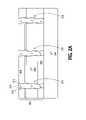
- FIG. 4is a top view of the structure of FIG. 2B .
- FIG. 2Bis a cross-section viewed along line 2 B- 2 B of FIG. 4 .
- slots 410are formed passing through dielectric layers 222 and conductive layers 224 in a direction substantially parallel to holes 226 , stopping substantially on the upper surface of source-select-gate portion 201 so that slots 410 extend to substantially the same level below the upper surface of memory cell portion 220 as do holes 226 .
- slots 410stop at an upper surface of conductive pillars 214 and an upper surface of cap layer 208 .
- Each slot 410is then filled with a dielectric material 415 , such as a high-density-plasma (HDP) oxide, spin-on dielectric material, e.g., hydrogen silsesquioxane (HSQ), hexamethyldisiloxane, octamethyltrisiloxane, etc., to form an isolation region 420
- a dielectric material 415such as a high-density-plasma (HDP) oxide, spin-on dielectric material, e.g., hydrogen silsesquioxane (HSQ), hexamethyldisiloxane, octamethyltrisiloxane, etc.
- Isolation regions 420cut each conductive layer 224 into electrically isolated activation lines, such as word lines, 424 , as shown in FIGS. 2B and 4 , that extend substantially perpendicularly into the plane of FIG. 2B .
- isolation regions 420divide conductive layer 2242 into a plurality of isolated word lines 424 2,1 , 424 2,2 , 424 2,3 , and 424 2,4 .
- Each isolation region 420extends between conductive pillars 230 in a direction transverse to the depth of that isolation region 420 , e.g., in a direction substantially parallel to the word-line direction indicated by arrows 430 .
- Each isolation region 420cuts through at least a portion of the charge trapping layers 228 overlying the conductive pillars 230 between which that isolation region 420 extends so that the each charge trapping layer 228 is not contiguous in a direction around a perimeter of the respective one of the filled holes 226 , as shown in FIG. 4 .
- Each isolation region 420forms a pair of charge traps 229 from each of the charge trapping layers 228 , with a charge trap 229 interposed between a side of a conductive pillar 230 and a word line 424 , as shown in FIGS. 2B and 4 .
- an isolation region 420may cut through oxide layer 232 , nitride layer 234 , and oxide layer 236 , as shown in FIG.
- an isolation region 420may cut through oxide layer 232 and nitride layer 234 of a charge trap 228 .
- holes 226are shown to have circular cross-sections in FIG. 4 , holes 226 may have oval or substantially square or rectangular cross-sections or the like.
- Cutting a charge trapping layer 228 with an isolation region 420forms a pair of isolated memory cells 450 1,2 , 450 2,2 , with memory cell 450 1,2 occurring at an intersection between a first side of a pillar 230 and word line 424 2,2 , and memory cell 450 2,2 occurring at an intersection between a second side, opposite the first side, of that pillar 230 and word line 424 2,3 , as shown in FIGS. 2B and 4 .
- the word lineforms a control gate of the memory cell 450 at that intersection. As shown in FIG.
- memory cells 450 1,1 and 450 1,2 respectively formed at the intersection of a first side of a pillar 230 and word lines 424 1,2 and 424 2,2form a first serially-coupled string, e.g., a first NAND string, of memory cells on the first side of that pillar 230
- memory cells 450 2,1 and 450 2,2 respectively formed at the intersection of the second side of that pillar 230 word lines 424 1,3 and 424 2,3form a second serially-coupled string, e.g., a second NAND string, of memory cells on the second side of that pillar 230
- memory cells of a serially-coupled stringmay alternate on opposing sides of a pillar 230 .
- memory cells 450 1,1 and 450 2,2 respectively formed at the intersection of a first side of a pillar 230 and word line 424 1,2 and at the intersection of a second side of that pillar 230 and word line 424 2,3may form a first serially-coupled string, e.g., a first NAND string, of memory cells on alternating sides of that pillar 230
- memory cells 450 2,1 and 450 1,2 respectively formed at the intersection of the second side of that pillar 230 and word lines 424 1,3 and at the intersection of the first side of that pillar 230 and word line 424 2,3may form a second serially-coupled string, e.g., a second NAND string, of memory cells on alternating sides of that pillar 230 .
- each memory cell 450may be a non-volatile SONOS flash memory cell that includes a portion of a word line 424 that forms a control gate of the memory cell 450 , a charge trap 228 , including an oxide layer 232 formed on the word line 424 , a nitride layer 234 formed on the oxide layer 232 , an oxide layer 236 formed on the nitride layer 234 , and a portion of a conductive pillar 230 formed on the oxide layer 236 .
- drain-select-gate portion 250 of the memory arrayis formed overlying the memory cell portion 220 of FIG. 2B , according to an embodiment.
- Drain-select-gate portion 250may be formed by forming a dielectric layer 252 , such as a pad oxide layer, e.g., a thermal oxide layer or a deposited silicon dioxide (SiO 2 ) layer, overlying the uppermost word lines 424 , e.g., word lines 424 2,1 , 424 2,2 , 424 2,3 , and 424 2,4 , the isolation region 420 between the uppermost word lines 424 , and conductive pillars 230 , as shown in FIG. 2C .
- a dielectric layer 252such as a pad oxide layer, e.g., a thermal oxide layer or a deposited silicon dioxide (SiO 2 ) layer
- a dielectric layer 254such as a nitride layer, e.g., a layer of silicon nitride, is formed overlying dielectric layer 252 .
- a dielectric layer 256e.g., similar to dielectric layer 252 , is formed overlying dielectric layer 254 .
- a conductive layer 258e.g., similar to conductive layer 204 as described above in conjunction with FIG. 2A , is formed overlying dielectric layer 256 .
- a dielectric layer 260e.g., similar to dielectric layer 252 , is formed overlying conductive layer 258 .
- a dielectric layer 262e.g., similar to dielectric layer 254 , is formed overlying dielectric layer 260 .
- a dielectric layer 264e.g., similar to dielectric layer 252 , is formed overlying dielectric layer 262 .
- holes 266are formed passing through dielectric layer 264 , dielectric layer 262 , dielectric layer 260 , conductive layer 258 , dielectric layer 254 , and dielectric layer 252 , e.g., stopping substantially on conductive pillars 230 .
- holes 266may be aligned with conductive pillars 230 , as shown in FIG. 2C .
- Holes 266may be formed by patterning dielectric layer 264 and removing portions of dielectric layer 264 , dielectric layer 262 , dielectric layer 260 , conductive layer 258 , dielectric layer 256 , dielectric layer 254 , and dielectric layer 252 corresponding to the holes 266 exposed by the patterned dielectric layer 264 by etching, for example. Note that each of holes 266 exposes an edge of dielectric layer 264 , dielectric layer 262 , dielectric layer 260 , conductive layer 258 , dielectric layer 254 , and dielectric layer 252 and an upper surface of a conductive pillar 230 .
- Each of holes 266is then lined with a dielectric layer 268 , such as an oxide layer, e.g., using low pressure chemical vapor deposition (LPCVD).
- dielectric layer 268is formed on the exposed edges of dielectric layer 264 , dielectric layer 262 , dielectric layer 260 , conductive layer 258 , dielectric layer 254 , and dielectric layer 252 .
- the remaining portion of each of holes 266is then filled with a conductive layer, e.g., a conductive pillar, such as a plug, 270 , e.g., of polysilicon, that overlies dielectric layer 268 .
- conductive pillar 270is conductively doped to an n 31 conductivity type. Then, for example, ion implantation at a first power setting may be used to convert a portion of conductive pillar 270 at the level of dielectric layers 252 , 254 , and 256 to an n + conductivity type, as shown in FIG. 2C . Ion implantation at a second power setting may be used to convert a portion of conductive pillar 270 at the level of dielectric layers 260 , 262 , and 264 to an n + conductivity type, for example, as shown in FIG. 2C .
- trenches 274are formed passing through dielectric layer 264 , dielectric layer 262 , dielectric layer 260 , conductive layer 258 , dielectric layer 256 , dielectric layer 254 , and dielectric layer 252 , stopping substantially on the uppermost word lines 424 , e.g., word lines 424 2,1 , 424 2,2 , 424 2,3 , and 424 2,4 of FIG. 2C .
- Trenches 274may be formed by patterning dielectric layer 264 and removing portions of dielectric layer 264 , dielectric layer 262 , dielectric layer 260 , conductive layer 258 , dielectric layer 256 , dielectric layer 254 , and dielectric layer 252 corresponding to the trenches 274 exposed by the patterned dielectric layer 264 by etching, for example.
- Each trench 274is then filled with a dielectric material 276 , such as a high-density-plasma (HDP) oxide, spin-on dielectric material, e.g., hydrogen silsesquioxane (HSQ), hexamethyldisiloxane, octamethyltrisiloxane, etc., to form isolation regions 278 .
- Isolation regions 278define a control gate, such as a select gate 279 , at each intersection of the remaining portions of conductive layer 258 and a conductive pillar 270 , as shown in FIG. 2C .
- a drain select transistor 280such as a field effect transistor (FET) is formed at each intersection of a conductive pillar 270 and conductive layer 258 , where conductive layer 258 , dielectric layer 268 , and conductive pillar 270 respectively form the select gate, gate dielectric, and channel, of each drain select transistor 280 .
- each drain select transistor 280has a gate dielectric 268 on a conductive pillar 270 and a select gate 279 on the gate dielectric 268 .
- Each select gate 279forms a portion of a drain select line 282 , indicated by a dashed line in FIG. 4 .
- Each drain select line 282overlies and is substantially parallel to a dielectric-filled slot 410 , as shown in FIG. 4 .
- a conductive layer 286e.g., a metal layer, such as aluminum, is formed overlying an upper surface of each isolation region 278 , an upper surface of dielectric layer 264 , and an upper surface of each conductive pillar 270 , as shown in FIG. 2C .
- Conductive layer 286is patterned, etched, and processed, e.g., using standard processing, to produce individual data lines, such as bit lines 290 , shown as dashed lines in FIG. 4 , therefrom.
- Bit lines 290are substantially orthogonal to select lines 282 and dielectric-filled slots 410 , as shown in FIG. 4 .
- FIG. 2Cshows a serially-coupled string of memory cells 450 1,1 and 450 1,2 located on one side of a conductive pillar 230 and interposed between source select transistor 216 and a drain select transistor 280 , and a serially-coupled string of memory cells 450 2,1 and 450 2,2 , located on the opposite side of that conductive pillar 230 and interposed between source select transistor 216 and a drain select transistor 280 .
- the common pillar 230couples the memory cells 450 1,1 and 450 1,2 in series and the memory cells 450 2,1 and 450 2,2 in series.
- the number of memory cells in a serially-coupled string of memory cellsmay be some power of 2, such as 8, 16, 32, 64, etc.
- a source select transistor 216is coupled to each serially-coupled string of memory cells through a conductive pillar 214
- a drain select transistor 280is coupled to each serially-coupled string of memory cells through a conductive pillar 270 , as shown in FIG. 2C .
- Each source select transistor 216selectively couples the lower end of each conductive pillar 230 and thus the serially-coupled string of memory cells on either side of that conductive pillar 230 to source line 200 , as shown in FIG. 2C .
- Each drain select transistor 280selectively couples the upper end of each conductive pillar 230 and thus the serially-coupled string of memory cells on either side of that conductive pillar 230 to a bit line 290 .
Landscapes
- Non-Volatile Memory (AREA)
- Semiconductor Memories (AREA)
Abstract
Description
- The present disclosure relates generally to memory arrays and in particular at least one embodiment of the present disclosure relates to a memory array with a pair of memory-cell strings to a single conductive pillar.
- Memory devices are typically provided as internal, semiconductor, integrated circuits in computers or other electronic devices. There are many different types of memory including random-access memory (RAM), read only memory (ROM), dynamic random access memory (DRAM), synchronous dynamic random access memory (SDRAM), and flash memory.
- Flash memory devices have developed into a popular source of non-volatile memory for a wide range of electronic applications. Non-volatile memory is memory that can retain its data values for some extended period without the application of power. Flash memory devices typically use a one-transistor memory cell that allows for high memory densities, high reliability, and low power consumption. Changes in threshold voltage of the cells, through programming of charge storage nodes, such as floating gates or trapping layers or other physical phenomena, determine the data value of each cell. By defining two or more ranges of threshold voltages to correspond to individual data values, one or more bits of information may be stored on each cell. Common uses for flash memory and other non-volatile memory include personal computers, personal digital assistants (PDAs), digital cameras, digital media players, digital recorders, games, appliances, vehicles, wireless devices, mobile telephones and removable memory modules, and the uses for non-volatile memory continue to expand.
- Flash memory typically utilizes one of two basic architectures known as NOR flash and NAND flash. The designation is derived from the logic used to read the devices. In NOR flash architecture, a column of memory cells are coupled in parallel with each memory cell coupled to a bit line. In NAND flash architecture, a column of memory cells are coupled in series with only the first memory cell of the column coupled to a bit line.
- One common type of flash memory is a nitride read only memory (NROM), sometimes referred to as semiconductor-oxide-nitride-oxide-semiconductor (SONOS) memory. Such devices generally include silicon nitride (Si3N4) as a charge-trapping node, although other dielectric materials may be utilized. By accumulating charge in, or discharging, the charge-trapping node within a memory cell, the threshold voltage of that memory cell may be altered.
- In order for memory manufacturers to remain competitive, memory designers are constantly trying to increase the density of memory devices. Increasing the density of a flash memory device generally requires reducing spacing between memory cells and/or making memory cells smaller. Smaller dimensions of many device elements may cause operational problems with the cell. For example, the channel between the source/drain regions becomes shorter, possibly causing severe short channel effects.
- One way of increasing the density of memory devices is to form multi-layered memory arrays, e.g., often referred to as three-dimensional memory arrays. For example, one type of three-dimensional memory array includes a plurality of horizontal layers of traditional two-dimensional arrays, such as NAND or NOR memory arrays, stacked vertically one atop the other, with the memory cells of each memory array being silicon-on-sapphire transistors, silicon-on-insulator transistors, thin film transistors, thermoelectric polymer transistors, semiconductor-oxide-nitride-oxide-semiconductor transistors, etc. Another type of three-dimensional memory array includes pillars of stacked memory elements, such as vertical NAND strings that pass vertically through multi-stacked layers of electrode material, where each memory element is a semiconductor-oxide-nitride-oxide-semiconductor transistor, for example.
- For the reasons stated above, and for other reasons stated below which will become apparent to those skilled in the art upon reading and understanding the present specification, there is a need in the art for alternative three-dimensional memory arrays.
FIG. 1 is a simplified block diagram of an embodiment of a NAND flash memory device, according to an embodiment of the disclosure.FIGS. 2A-2C are cross-sectional views of a portion of a memory array at various stages of fabrication in accordance with another embodiment of the disclosure.FIG. 3 is an enlarged view ofregion 300 ofFIG. 2B , according to another embodiment of the disclosure.FIG. 4 is a top view of the structure ofFIG. 2B , according to another embodiment of the disclosure.- In the following detailed description, reference is made to the accompanying drawings that form a part hereof, and in which is shown, by way of illustration, specific embodiments. In the drawings, like numerals describe substantially similar components throughout the several views. Other embodiments may be utilized and structural, logical, and electrical changes may be made without departing from the scope of the present disclosure. Use the following if applicable: The term wafer or substrate used in the following description includes any base semiconductor structure. Both are to be understood as including silicon-on-sapphire (SOS) technology, silicon-on-insulator (SOI) technology, thin film transistor (TFT) technology, doped and undoped semiconductors, epitaxial layers of a silicon supported by a base semiconductor structure, as well as other semiconductor structures well known to one skilled in the art. Furthermore, when reference is made to a wafer or substrate in the following description, previous process steps may have been utilized to form regions/junctions in the base semiconductor structure, and terms wafer or substrate include the underlying layers containing such regions/junctions. The following detailed description is, therefore, not to be taken in a limiting sense, and the scope of the present disclosure is defined only by the appended claims and equivalents thereof.
FIG. 1 is a simplified block diagram of a NANDflash memory device 100 in communication with aprocessor 130 as part of an electronic system, according to an embodiment. Theprocessor 130 may be a memory controller or other external host device.Memory device 100 includes an array ofmemory cells 104 formed in accordance with embodiments of the disclosure. Arow decoder 108 and acolumn decoder 110 are provided to decode address signals. Address signals are received and decoded to accessmemory array 104.Memory device 100 also includes input/output (I/O)control circuitry 112 to manage input of commands, addresses and data to thememory device 100 as well as output of data and status information from thememory device 100. Anaddress register 114 is in communication with I/O control circuitry 112, androw decoder 108 andcolumn decoder 110 to latch the address signals prior to decoding. Acommand register 124 is in communication with I/O control circuitry 112 andcontrol logic 116 to latch incoming commands.Control logic 116 controls access to thememory array 104 in response to the commands and generates status information for theexternal processor 130. Thecontrol logic 116 is in communication withrow decoder 108 andcolumn decoder 110 to control therow decoder 108 andcolumn decoder 110 in response to the addresses.Control logic 116 is also in communication with acache register 118. Cache register118 latches data, either incoming or outgoing, as directed bycontrol logic 116 to temporarily store data while thememory array 104 is busy writing or reading, respectively, other data. For one embodiment,control logic 116 may include one or more circuits adapted to produce a particular and predictable outcome or set of outcomes in response to one or more input events. During a write operation, data is passed from thecache register 118 todata register 120 for transfer to thememory array 104; then new data is latched in thecache register 118 from the I/O control circuitry 112. During a read operation, data is passed from thecache register 118 to the I/O control circuitry 112 for output to theexternal processor 130; then new data is passed from thedata register 120 to thecache register 118. A status register122 is in communication with I/O control circuitry 112 andcontrol logic 116 to latch the status information for output to theprocessor 130.Memory device 100 receives control signals atcontrol logic 116 fromprocessor 130 over acontrol link 132. The control signals may include at least chip enable CE #, a command latch enable CLE, an address latch enable ALE, and a write enable WE #.Memory device 100 receives command signals (which represent commands), address signals (which represent addresses), and data signals (which represent data) fromprocessor 130 over a multiplexed input/output (I/O)bus 134 and outputs data toprocessor 130 over I/O bus 134.- For example, the commands are received over input/output (I/O) pins [0:7] of I/
O bus 134 at I/O control circuitry 112 and are written intocommand register 124. The addresses are received over input/output (I/O) pins [0:7] ofbus 134 at I/O control circuitry 112 and are written intoaddress register 114. The data are received over input/output (I/O) pins [0:7] for an 8-bit device or input/output (I/O) pins [0:15] for a 16-bit device at I/O control circuitry 112 and are written intocache register 118. The data are subsequently written intodata register 120 forprogramming memory array 104. For another embodiment,cache register 118 may be omitted, and the data are written directly intodata register 120. Data are also output over input/output (I/O) pins [0:7] for an 8-bit device or input/output (I/O) pins [0:15] for a 16-bit device. - It will be appreciated by those skilled in the art that additional circuitry and signals can be provided, and that the memory device of
FIG. 1 has been simplified. It should be recognized that the functionality of the various block components described with reference toFIG. 1 may not be segregated to distinct components or component portions of an integrated circuit device. For example, a single component or component portion of an integrated circuit device could be adapted to perform the functionality of more than one block component ofFIG. 1 . Alternatively, one or more components or component portions of an integrated circuit device could be combined to perform the functionality of a single block component ofFIG. 1 . - Additionally, while specific I/O pins are described in accordance with popular conventions for receipt and output of the various signals, it is noted that other combinations or numbers of I/O pins may be used in the various embodiments.
FIGS. 2A-2C are cross sectional views of a portion of a memory array, such asmemory array 104 ofFIG. 1 , during various stages of fabrication, according to an embodiment.FIG. 2A shows a cross-section of a source-select-gate portion 201 of the memory array after several processing steps have been performed. In general, the formation of the structure ofFIG. 2A may include forming adielectric layer 202 overlying asemiconductor substrate 200, such as a silicon-containing substrate, e.g., a P-type monocrystalline silicon substrate, as shown inFIG. 2A . For one embodiment,semiconductor substrate 200 forms asource line 200 of the memory array.Dielectric layer 202 may be an oxide-nitride-oxide (ONO) layer, with a first oxide layer in contact withsource line 200, the nitride layer overlying and in contact with the first oxide layer, and a second oxide layer overlying and in contact with the nitride layer.- A
conductive layer 204 is formed overlyingdielectric layer 202.Conductive layer 204 may be of polysilicon, such as conductively doped P-type polysilicon, as shown inFIG. 2A . Alternatively,conductive layer 204 may be a metal-containing layer, such as a refractory metal silicide layer. The metals of chromium (Cr), cobalt (Co), hafnium (Hf), molybdenum (Mo), niobium (Nb), tantalum (Ta), titanium (Ti), tungsten (W), vanadium (V) and zirconium (Zr) are generally recognized as refractory metals. - A
dielectric layer 206, such as a pad oxide layer, e.g., a thermal oxide layer or a deposited silicon dioxide (SiO2) layer, is formed overlyingconductive layer 204. Acap 208, such as a nitride cap, e.g., of silicon nitride, is formed overlyingdielectric layer 206. - After forming
cap 208,holes 210 are formed passing throughcap 208,dielectric layer 206,conductive layer 204, anddielectric layer 202, stopping substantially onsource line 200.Holes 210 may be formed by patterningcap layer 208 and removing portions ofcap layer 208,dielectric layer 206,conductive layer 204, anddielectric layer 202 corresponding to theholes 210 exposed by the patternedcap layer 208 by etching, for example. Note that each ofholes 210 exposes an edge ofcap layer 208,dielectric layer 206, conductivelayer cap layer 204, anddielectric layer 202 and portion ofsource line 200. Each ofholes 210 is then lined with adielectric layer 212, such as an oxide layer, e.g., using low pressure chemical vapor deposition (LPCVD). For example,dielectric layer 212 is formed on the exposed edges ofcap 208,dielectric layer 206,conductive layer 204, anddielectric layer 202. The remaining portion of each ofholes 210 is then filled with a conductive layer, e.g., a conductive pillar, such as a plug,214, e.g., of polysilicon, that overliesdielectric layer 212. - For one embodiment,
conductive pillar 214 is conductively doped to an n− conductivity type. Then, for example, ion implantation at a first power setting may be used to convert a portion ofconductive pillar 214 at the level ofdielectric layer 202 to an n+ conductivity type, as shown inFIG. 2A . Ion implantation at a second power setting may be used to convert a portion ofconductive pillar 214 at the level ofcap layer 208 to an n+ conductivity type, for example, as shown inFIG. 2A . - A source
select transistor 216, such as a field effect transistor (FET), is formed at each intersection of aconductive pillar 214 andconductive layer 204, whereconductive layer 204,dielectric layer 212, andconductive pillar 214 respectively form the control gate (which can also be referred to as a select gate), gate dielectric, and channel, of eachselect transistor 216. In other words, each sourceselect transistor 216 has agate dielectric 212 on aconductive pillar 214 and aselect gate 204 on thegate dielectric 212. Eachselect gate 204 forms a portion of a source select line extending substantially perpendicularly into the plane ofFIG. 2A (not shown). - In
FIG. 2B , amemory cell portion 220 of the memory array is formed overlying the source-select-gate portion 201 ofFIG. 2A .Memory cell portion 220 may be formed by forming a dielectric layer222, e.g., dielectric layer2221, such as a pad oxide layer, e.g., a thermal oxide layer or a deposited silicon dioxide (SiO2) layer, overlyingcap layer 208. A conductive layer224, e.g., conductive layer2241, is formed overlying dielectric layer2221. Conductive layer224 may be of polysilicon, such as conductively doped P-type polysilicon. Alternatively, conductive layer224 may be a metal-containing layer, such as a refractory metal silicide layer. Another dielectric layer222, e.g., dielectric layer2222, is formed overlying conductive layer2241, and another conductive layer224, e.g., conductive layer2242, is formed overlying dielectric layer2222, as shown inFIG. 2B . For one embodiment, dielectric layers222 and conductive layers224 may alternate, as shown inFIG. 2B , untilmemory cell portion 220 includes up to a certain number, e.g., N, where N is generally some power of two, such as 8, 16, 32, 64, etc., of alternating dielectric layers222 and conductive layers224 overlying source-select-gate portion 201. Holes 226 are formed passing through dielectric layers222 and conductive layers224, stopping substantially on an upper surface of source-select-gate portion 201 so thatholes 226 are substantially aligned withconductive pillars 214, as shown inFIG. 2B . For example, holes226 may stop at an upper surface ofconductive pillars 214.Holes 226 may be formed by patterning the uppermost conductive layer224, e.g., conductive layer2242inFIG. 2B , and removing portions of dielectric layers222 and conductive layers224 corresponding to theholes 226 exposed by the patterned conductive layer224 by etching, for example. Note that each ofholes 226 exposes an edge of each dielectric layer222 and each conductive layer224 and an upper surface of aconductive pillar 214.- Each of
holes 226 may be lined with acharge trapping layer 228, e.g., using low pressure chemical vapor deposition (LPCVD). For example,charge trapping layer 228 is formed on the exposed edges of each conductive layer224 and each dielectric layer222. The remaining portion of each ofholes 226 is then filled with a conductive layer, e.g., a conductive pillar, such as a plug,230, e.g., of polysilicon, that overliescharge trapping layer 228 so that eachconductive pillar 230 contacts a respective one ofconductive pillars 214, as shown inFIG. 2B . FIG. 3 is an enlarged view ofregion 300 ofFIG. 2B , illustrating the structure ofcharge trapping layer 228, according to another embodiment. For one embodiment,conductive pillar 230,charge trapping layer 228, and conductive layer224 form a semiconductor-oxide-nitride-oxide-semiconductor (SONOS) structure. For example,charge trapping layer 228 may include anoxide layer 232 formed on conductive layer224, anitride layer 234 formed onoxide layer 232, and anoxide layer 236 formed onnitride layer 234, as shown inFIG. 3 . Therefore, lining eachhole 226 includes formingoxide layer 232 on the sidewalls of eachhole 226, e.g., using LPCVD, formingnitride layer 234 onoxide layer 232, e.g., using LPCVD, and formingoxide layer 236 onnitride layer 234, e.g., using LPCVD.Conductive pillar 230 is then formed onoxide layer 236 so as to fill the remainder of eachhole 226.FIG. 4 is a top view of the structure ofFIG. 2B . In other words,FIG. 2B is a cross-section viewed along line2B-2B ofFIG. 4 . For one embodiment,slots 410 are formed passing through dielectric layers222 and conductive layers224 in a direction substantially parallel toholes 226, stopping substantially on the upper surface of source-select-gate portion 201 so thatslots 410 extend to substantially the same level below the upper surface ofmemory cell portion 220 as do holes226. For example,slots 410 stop at an upper surface ofconductive pillars 214 and an upper surface ofcap layer 208. Eachslot 410 is then filled with adielectric material 415, such as a high-density-plasma (HDP) oxide, spin-on dielectric material, e.g., hydrogen silsesquioxane (HSQ), hexamethyldisiloxane, octamethyltrisiloxane, etc., to form anisolation region 420Isolation regions 420 cut each conductive layer224 into electrically isolated activation lines, such as word lines,424, as shown inFIGS. 2B and 4 , that extend substantially perpendicularly into the plane ofFIG. 2B . For example,isolation regions 420 divideconductive layer 2242 into a plurality of isolated word lines4242,1,4242,2,4242,3, and4242,4. Eachisolation region 420 extends betweenconductive pillars 230 in a direction transverse to the depth of thatisolation region 420, e.g., in a direction substantially parallel to the word-line direction indicated byarrows 430.- Each
isolation region 420 cuts through at least a portion of the charge trapping layers228 overlying theconductive pillars 230 between which thatisolation region 420 extends so that the eachcharge trapping layer 228 is not contiguous in a direction around a perimeter of the respective one of the filledholes 226, as shown inFIG. 4 . Eachisolation region 420 forms a pair of charge traps229 from each of the charge trapping layers228, with acharge trap 229 interposed between a side of aconductive pillar 230 and a word line424, as shown inFIGS. 2B and 4 . For example, anisolation region 420 may cut throughoxide layer 232,nitride layer 234, andoxide layer 236, as shown inFIG. 4 . Alternatively, anisolation region 420 may cut throughoxide layer 232 andnitride layer 234 of acharge trap 228. Althoughholes 226 are shown to have circular cross-sections inFIG. 4 , holes226 may have oval or substantially square or rectangular cross-sections or the like. - Cutting a
charge trapping layer 228 with anisolation region 420 forms a pair of isolated memory cells4501,2,4502,2, with memory cell4501,2occurring at an intersection between a first side of apillar 230 and word line4242,2, and memory cell4502,2occurring at an intersection between a second side, opposite the first side, of thatpillar 230 and word line4242,3, as shown inFIGS. 2B and 4 . At each intersection between a side of a conductive pillar and a word line424, the word line forms a control gate of the memory cell450 at that intersection. As shown inFIG. 2B , memory cells4501,1and4501,2respectively formed at the intersection of a first side of apillar 230 and word lines4241,2and4242,2form a first serially-coupled string, e.g., a first NAND string, of memory cells on the first side of thatpillar 230, and memory cells4502,1and4502,2respectively formed at the intersection of the second side of thatpillar 230 word lines4241,3and4242,3form a second serially-coupled string, e.g., a second NAND string, of memory cells on the second side of thatpillar 230. Alternatively, memory cells of a serially-coupled string may alternate on opposing sides of apillar 230. For example, memory cells4501,1and4502,2respectively formed at the intersection of a first side of apillar 230 and word line4241,2and at the intersection of a second side of thatpillar 230 and word line4242,3may form a first serially-coupled string, e.g., a first NAND string, of memory cells on alternating sides of thatpillar 230, and memory cells4502,1and4501,2respectively formed at the intersection of the second side of thatpillar 230 and word lines4241,3and at the intersection of the first side of thatpillar 230 and word line4242,3may form a second serially-coupled string, e.g., a second NAND string, of memory cells on alternating sides of thatpillar 230. For one embodiment, each memory cell450 may be a non-volatile SONOS flash memory cell that includes a portion of a word line424 that forms a control gate of the memory cell450, acharge trap 228, including anoxide layer 232 formed on the word line424, anitride layer 234 formed on theoxide layer 232, anoxide layer 236 formed on thenitride layer 234, and a portion of aconductive pillar 230 formed on theoxide layer 236. - In
FIG. 2C , a drain-select-gate portion 250 of the memory array is formed overlying thememory cell portion 220 ofFIG. 2B , according to an embodiment. Drain-select-gate portion 250 may be formed by forming adielectric layer 252, such as a pad oxide layer, e.g., a thermal oxide layer or a deposited silicon dioxide (SiO2) layer, overlying the uppermost word lines424, e.g., word lines4242,1,4242,2,4242,3, and4242,4, theisolation region 420 between the uppermost word lines424, andconductive pillars 230, as shown inFIG. 2C . - A
dielectric layer 254, such as a nitride layer, e.g., a layer of silicon nitride, is formed overlyingdielectric layer 252. Adielectric layer 256, e.g., similar todielectric layer 252, is formed overlyingdielectric layer 254. Aconductive layer 258, e.g., similar toconductive layer 204 as described above in conjunction withFIG. 2A , is formed overlyingdielectric layer 256. Adielectric layer 260, e.g., similar todielectric layer 252, is formed overlyingconductive layer 258. A dielectric layer262, e.g., similar todielectric layer 254, is formed overlyingdielectric layer 260. Adielectric layer 264, e.g., similar todielectric layer 252, is formed overlying dielectric layer262. - After forming
dielectric layer 264,holes 266 are formed passing throughdielectric layer 264, dielectric layer262,dielectric layer 260,conductive layer 258,dielectric layer 254, anddielectric layer 252, e.g., stopping substantially onconductive pillars 230. For example holes266 may be aligned withconductive pillars 230, as shown inFIG. 2C .Holes 266 may be formed by patterningdielectric layer 264 and removing portions ofdielectric layer 264, dielectric layer262,dielectric layer 260,conductive layer 258,dielectric layer 256,dielectric layer 254, anddielectric layer 252 corresponding to theholes 266 exposed by the patterneddielectric layer 264 by etching, for example. Note that each ofholes 266 exposes an edge ofdielectric layer 264, dielectric layer262,dielectric layer 260,conductive layer 258,dielectric layer 254, anddielectric layer 252 and an upper surface of aconductive pillar 230. Each ofholes 266 is then lined with adielectric layer 268, such as an oxide layer, e.g., using low pressure chemical vapor deposition (LPCVD). For example,dielectric layer 268 is formed on the exposed edges ofdielectric layer 264, dielectric layer262,dielectric layer 260,conductive layer 258,dielectric layer 254, anddielectric layer 252. The remaining portion of each ofholes 266 is then filled with a conductive layer, e.g., a conductive pillar, such as a plug,270, e.g., of polysilicon, that overliesdielectric layer 268. - For one embodiment,
conductive pillar 270 is conductively doped to an n31 conductivity type. Then, for example, ion implantation at a first power setting may be used to convert a portion ofconductive pillar 270 at the level ofdielectric layers FIG. 2C . Ion implantation at a second power setting may be used to convert a portion ofconductive pillar 270 at the level ofdielectric layers FIG. 2C . - For one embodiment,
trenches 274 are formed passing throughdielectric layer 264, dielectric layer262,dielectric layer 260,conductive layer 258,dielectric layer 256,dielectric layer 254, anddielectric layer 252, stopping substantially on the uppermost word lines424, e.g., word lines4242,1,4242,2,4242,3, and4242,4ofFIG. 2C .Trenches 274 may be formed by patterningdielectric layer 264 and removing portions ofdielectric layer 264, dielectric layer262,dielectric layer 260,conductive layer 258,dielectric layer 256,dielectric layer 254, anddielectric layer 252 corresponding to thetrenches 274 exposed by the patterneddielectric layer 264 by etching, for example. Eachtrench 274 is then filled with adielectric material 276, such as a high-density-plasma (HDP) oxide, spin-on dielectric material, e.g., hydrogen silsesquioxane (HSQ), hexamethyldisiloxane, octamethyltrisiloxane, etc., to formisolation regions 278.Isolation regions 278 define a control gate, such as aselect gate 279, at each intersection of the remaining portions ofconductive layer 258 and aconductive pillar 270, as shown inFIG. 2C . - A drain
select transistor 280, such as a field effect transistor (FET), is formed at each intersection of aconductive pillar 270 andconductive layer 258, whereconductive layer 258,dielectric layer 268, andconductive pillar 270 respectively form the select gate, gate dielectric, and channel, of each drainselect transistor 280. In other words, each drainselect transistor 280 has agate dielectric 268 on aconductive pillar 270 and aselect gate 279 on thegate dielectric 268. Eachselect gate 279 forms a portion of a drainselect line 282, indicated by a dashed line inFIG. 4 . Each drainselect line 282 overlies and is substantially parallel to a dielectric-filledslot 410, as shown inFIG. 4 . - A
conductive layer 286, e.g., a metal layer, such as aluminum, is formed overlying an upper surface of eachisolation region 278, an upper surface ofdielectric layer 264, and an upper surface of eachconductive pillar 270, as shown inFIG. 2C .Conductive layer 286 is patterned, etched, and processed, e.g., using standard processing, to produce individual data lines, such asbit lines 290, shown as dashed lines inFIG. 4 , therefrom.Bit lines 290 are substantially orthogonal to selectlines 282 and dielectric-filledslots 410, as shown inFIG. 4 . - Note that the memory cells450 on each side of a
conductive pillar 230 and dielectric-filled slot410 (FIG. 4 ) form a serially-coupled string of memory cells450 interposed between a sourceselect transistor 216 and a drainselect transistor 280. For example,FIG. 2C shows a serially-coupled string of memory cells4501,1and4501,2located on one side of aconductive pillar 230 and interposed between sourceselect transistor 216 and a drainselect transistor 280, and a serially-coupled string of memory cells4502,1and4502,2, located on the opposite side of thatconductive pillar 230 and interposed between sourceselect transistor 216 and a drainselect transistor 280. Thecommon pillar 230 couples the memory cells4501,1and4501,2in series and the memory cells4502,1and4502,2in series. For some embodiments, the number of memory cells in a serially-coupled string of memory cells may be some power of 2, such as 8, 16, 32, 64, etc. - A source
select transistor 216 is coupled to each serially-coupled string of memory cells through aconductive pillar 214, and a drainselect transistor 280 is coupled to each serially-coupled string of memory cells through aconductive pillar 270, as shown inFIG. 2C . Each sourceselect transistor 216 selectively couples the lower end of eachconductive pillar 230 and thus the serially-coupled string of memory cells on either side of thatconductive pillar 230 to sourceline 200, as shown inFIG. 2C . Each drainselect transistor 280 selectively couples the upper end of eachconductive pillar 230 and thus the serially-coupled string of memory cells on either side of thatconductive pillar 230 to abit line 290. - Although specific embodiments have been illustrated and described herein, it will be appreciated by those of ordinary skill in the art that any arrangement that is calculated to achieve the same purpose may be substituted for the specific embodiments shown. Many adaptations of the embodiments will be apparent to those of ordinary skill in the art. Accordingly, this application is intended to cover any adaptations or variations of the embodiments. It is manifestly intended that the embodiments be limited only by the following claims and equivalents thereof.
Claims (25)
Priority Applications (15)
| Application Number | Priority Date | Filing Date | Title |
|---|---|---|---|
| US12/047,414US7906818B2 (en) | 2008-03-13 | 2008-03-13 | Memory array with a pair of memory-cell strings to a single conductive pillar |
| EP09719271.0AEP2253014B1 (en) | 2008-03-13 | 2009-03-12 | Memory array with a pair of memory-cell strings to a single conductive pillar |
| JP2010550856AJP5517073B2 (en) | 2008-03-13 | 2009-03-12 | Memory array with a pair of memory cell strings on a single conductive column |
| PCT/US2009/036929WO2009114675A2 (en) | 2008-03-13 | 2009-03-12 | Memory array with a pair of memory-cell strings to a single conductive pillar |
| KR1020107022780AKR101097535B1 (en) | 2008-03-13 | 2009-03-12 | Memory array with a pair of memory-cell strings to a single conductive pillar |
| CN200980108602.6ACN101971324B (en) | 2008-03-13 | 2009-03-12 | Memory array with a pair of memory-cell strings to a single conductive pillar |
| US13/047,215US8329513B2 (en) | 2008-03-13 | 2011-03-14 | Methods of forming a memory array with a pair of memory-cell strings to a single conductive pillar |
| US13/676,407US9147693B2 (en) | 2008-03-13 | 2012-11-14 | Memory array with a pair of memory-cell strings to a single conductive pillar |
| US14/820,027US9455266B2 (en) | 2008-03-13 | 2015-08-06 | Memory array with a pair of memory-cell strings to a single conductive pillar |
| US15/246,847US9768194B2 (en) | 2008-03-13 | 2016-08-25 | Methods of forming memory arrays |
| US15/691,794US10522559B2 (en) | 2008-03-13 | 2017-08-31 | Systems including memory cells on opposing sides of a pillar |
| US16/545,504US10957709B2 (en) | 2008-03-13 | 2019-08-20 | Systems including memory cells on opposing sides of a pillar |
| US16/736,297US11398493B2 (en) | 2008-03-13 | 2020-01-07 | Arrays of memory cells including pairs of memory cells having respective charge storage nodes between respective access lines |
| US17/872,158US12262536B2 (en) | 2008-03-13 | 2022-07-25 | Arrays of memory cells including pairs of memory cells having respective charge storage nodes between respective access lines |
| US19/021,859US20250234546A1 (en) | 2008-03-13 | 2025-01-15 | Methods of forming arrays of memory cells including pairs of memory cells having respective charge storage nodes between respective access lines |
Applications Claiming Priority (1)
| Application Number | Priority Date | Filing Date | Title |
|---|---|---|---|
| US12/047,414US7906818B2 (en) | 2008-03-13 | 2008-03-13 | Memory array with a pair of memory-cell strings to a single conductive pillar |
Related Child Applications (1)
| Application Number | Title | Priority Date | Filing Date |
|---|---|---|---|
| US13/047,215DivisionUS8329513B2 (en) | 2008-03-13 | 2011-03-14 | Methods of forming a memory array with a pair of memory-cell strings to a single conductive pillar |
Publications (2)
| Publication Number | Publication Date |
|---|---|
| US20090230454A1true US20090230454A1 (en) | 2009-09-17 |
| US7906818B2 US7906818B2 (en) | 2011-03-15 |
Family
ID=41062073
Family Applications (10)
| Application Number | Title | Priority Date | Filing Date |
|---|---|---|---|
| US12/047,414Active2028-09-04US7906818B2 (en) | 2008-03-13 | 2008-03-13 | Memory array with a pair of memory-cell strings to a single conductive pillar |
| US13/047,215ActiveUS8329513B2 (en) | 2008-03-13 | 2011-03-14 | Methods of forming a memory array with a pair of memory-cell strings to a single conductive pillar |
| US13/676,407Active2028-12-18US9147693B2 (en) | 2008-03-13 | 2012-11-14 | Memory array with a pair of memory-cell strings to a single conductive pillar |
| US14/820,027ActiveUS9455266B2 (en) | 2008-03-13 | 2015-08-06 | Memory array with a pair of memory-cell strings to a single conductive pillar |
| US15/246,847ActiveUS9768194B2 (en) | 2008-03-13 | 2016-08-25 | Methods of forming memory arrays |
| US15/691,794Active2028-07-04US10522559B2 (en) | 2008-03-13 | 2017-08-31 | Systems including memory cells on opposing sides of a pillar |
| US16/545,504ActiveUS10957709B2 (en) | 2008-03-13 | 2019-08-20 | Systems including memory cells on opposing sides of a pillar |
| US16/736,297Active2028-09-23US11398493B2 (en) | 2008-03-13 | 2020-01-07 | Arrays of memory cells including pairs of memory cells having respective charge storage nodes between respective access lines |
| US17/872,158Active2028-07-28US12262536B2 (en) | 2008-03-13 | 2022-07-25 | Arrays of memory cells including pairs of memory cells having respective charge storage nodes between respective access lines |
| US19/021,859PendingUS20250234546A1 (en) | 2008-03-13 | 2025-01-15 | Methods of forming arrays of memory cells including pairs of memory cells having respective charge storage nodes between respective access lines |
Family Applications After (9)
| Application Number | Title | Priority Date | Filing Date |
|---|---|---|---|
| US13/047,215ActiveUS8329513B2 (en) | 2008-03-13 | 2011-03-14 | Methods of forming a memory array with a pair of memory-cell strings to a single conductive pillar |
| US13/676,407Active2028-12-18US9147693B2 (en) | 2008-03-13 | 2012-11-14 | Memory array with a pair of memory-cell strings to a single conductive pillar |
| US14/820,027ActiveUS9455266B2 (en) | 2008-03-13 | 2015-08-06 | Memory array with a pair of memory-cell strings to a single conductive pillar |
| US15/246,847ActiveUS9768194B2 (en) | 2008-03-13 | 2016-08-25 | Methods of forming memory arrays |
| US15/691,794Active2028-07-04US10522559B2 (en) | 2008-03-13 | 2017-08-31 | Systems including memory cells on opposing sides of a pillar |
| US16/545,504ActiveUS10957709B2 (en) | 2008-03-13 | 2019-08-20 | Systems including memory cells on opposing sides of a pillar |
| US16/736,297Active2028-09-23US11398493B2 (en) | 2008-03-13 | 2020-01-07 | Arrays of memory cells including pairs of memory cells having respective charge storage nodes between respective access lines |
| US17/872,158Active2028-07-28US12262536B2 (en) | 2008-03-13 | 2022-07-25 | Arrays of memory cells including pairs of memory cells having respective charge storage nodes between respective access lines |
| US19/021,859PendingUS20250234546A1 (en) | 2008-03-13 | 2025-01-15 | Methods of forming arrays of memory cells including pairs of memory cells having respective charge storage nodes between respective access lines |
Country Status (6)
| Country | Link |
|---|---|
| US (10) | US7906818B2 (en) |
| EP (1) | EP2253014B1 (en) |
| JP (1) | JP5517073B2 (en) |
| KR (1) | KR101097535B1 (en) |
| CN (1) | CN101971324B (en) |
| WO (1) | WO2009114675A2 (en) |
Cited By (34)
| Publication number | Priority date | Publication date | Assignee | Title |
|---|---|---|---|---|
| US20100224924A1 (en)* | 2009-03-04 | 2010-09-09 | Innovative Silicon Isi Sa | Techniques for forming a contact to a buried diffusion layer in a semiconductor memory device |
| US20110316063A1 (en)* | 2010-06-28 | 2011-12-29 | Tang Sanh D | Three dimensional memory and methods of forming the same |
| US20120061741A1 (en)* | 2008-09-30 | 2012-03-15 | Samsung Electronics Co., Ltd. | Three-dimensional microelectronic devices including horizontal and vertical patterns |
| US20120139027A1 (en)* | 2010-12-02 | 2012-06-07 | Samsung Electronics Co., Ltd. | Vertical structure non-volatile memory devices including impurity providing layer |
| US8237213B2 (en) | 2010-07-15 | 2012-08-07 | Micron Technology, Inc. | Memory arrays having substantially vertical, adjacent semiconductor structures and the formation thereof |
| WO2013025710A1 (en)* | 2011-08-15 | 2013-02-21 | Micron Technology, Inc. | Apparatus and methods including source gates |
| US8446767B2 (en) | 2010-07-02 | 2013-05-21 | Micron Technology, Inc. | Memories and their formation |
| US20140104955A1 (en)* | 2012-10-11 | 2014-04-17 | Dong-Hun KWAK | Programming nonvolatile memory device using program voltage with variable offset |
| US8735902B2 (en) | 2010-05-10 | 2014-05-27 | Micron Technology, Inc. | Memories with memory arrays extending in opposite directions from a semiconductor and their formation |
| US9043537B1 (en) | 2013-11-21 | 2015-05-26 | Sandisk Technologies Inc. | Update block programming order |
| US9041090B2 (en) | 2013-05-15 | 2015-05-26 | Micron Technology, Inc. | Methods for forming a string of memory cells and apparatuses having a vertical string of memory cells including metal |
| US20150160893A1 (en)* | 2013-12-06 | 2015-06-11 | Sandisk Technologies Inc. | Lower Page Only Host Burst Writes |
| US20150179660A1 (en)* | 2013-12-19 | 2015-06-25 | SanDisk Technologies, Inc. | Three Dimensional NAND Device with Channel Located on Three Sides of Lower Select Gate and Method of Making Thereof |
| US9105737B2 (en)* | 2013-01-07 | 2015-08-11 | Micron Technology, Inc. | Semiconductor constructions |
| US9159845B2 (en) | 2013-05-15 | 2015-10-13 | Micron Technology, Inc. | Charge-retaining transistor, array of memory cells, and methods of forming a charge-retaining transistor |
| US9178077B2 (en) | 2012-11-13 | 2015-11-03 | Micron Technology, Inc. | Semiconductor constructions |
| US9219132B2 (en) | 2013-01-10 | 2015-12-22 | Micron Technology, Inc. | Transistors, semiconductor constructions, and methods of forming semiconductor constructions |
| US9219070B2 (en) | 2013-02-05 | 2015-12-22 | Micron Technology, Inc. | 3-D memory arrays |
| US20160056210A1 (en)* | 2014-08-19 | 2016-02-25 | Sandisk 3D Llc | Word line connection for memory device and method of making thereof |
| WO2016053453A1 (en)* | 2014-09-05 | 2016-04-07 | Sandisk Technologies Inc. | 3d semicircular vertical nand string with self aligned floating gate or charge trap cell memory cells and methods of fabricating and operating the same |
| WO2017087047A1 (en)* | 2015-11-20 | 2017-05-26 | Sandisk Technologies Llc | 3d semicircular vertical nand string with recessed inactive semiconductor channel sections |
| US20170179143A1 (en)* | 2014-10-03 | 2017-06-22 | Micron Technology, Inc. | Memory having a continuous channel |
| US9812463B2 (en) | 2016-03-25 | 2017-11-07 | Sandisk Technologies Llc | Three-dimensional memory device containing vertically isolated charge storage regions and method of making thereof |
| US20180076209A1 (en)* | 2015-11-23 | 2018-03-15 | Micron Technology, Inc. | Integrated Assemblies and Methods of Forming Integrated Assemblies |
| US9935124B2 (en) | 2015-11-25 | 2018-04-03 | Sandisk Technologies Llc | Split memory cells with unsplit select gates in a three-dimensional memory device |
| US9960180B1 (en) | 2017-03-27 | 2018-05-01 | Sandisk Technologies Llc | Three-dimensional memory device with partially discrete charge storage regions and method of making thereof |
| US9991277B1 (en) | 2016-11-28 | 2018-06-05 | Sandisk Technologies Llc | Three-dimensional memory device with discrete self-aligned charge storage elements and method of making thereof |
| US10541029B2 (en) | 2012-08-01 | 2020-01-21 | Micron Technology, Inc. | Partial block memory operations |
| US10586802B2 (en) | 2011-02-25 | 2020-03-10 | Micron Technology, Inc. | Charge storage apparatus and methods |
| US20200098767A1 (en)* | 2018-09-20 | 2020-03-26 | Toshiba Memory Corporation | Semiconductor memory device |
| CN113097214A (en)* | 2019-12-23 | 2021-07-09 | 旺宏电子股份有限公司 | Semiconductor device, array layout thereof and packaging structure comprising same |
| US20210391354A1 (en)* | 2020-06-15 | 2021-12-16 | Taiwan Semiconductor Manufacturing Company, Ltd. | Memory device |
| US11716847B2 (en)* | 2020-10-19 | 2023-08-01 | Yangtze Memory Technologies Co., Ltd. | Three-dimensional NAND memory device with split gates |
| US11961581B2 (en) | 2017-12-22 | 2024-04-16 | Micron Technology, Inc. | Assemblies comprising memory cells and select gates; and methods of forming assemblies |
Families Citing this family (117)
| Publication number | Priority date | Publication date | Assignee | Title |
|---|---|---|---|---|
| JP2009277770A (en)* | 2008-05-13 | 2009-11-26 | Toshiba Corp | Non-volatile semiconductor memory device and its production process |
| JP2011029234A (en)* | 2009-07-21 | 2011-02-10 | Toshiba Corp | Nonvolatile semiconductor memory device |
| JP2011138945A (en)* | 2009-12-28 | 2011-07-14 | Toshiba Corp | Nonvolatile semiconductor memory device |
| KR101149619B1 (en)* | 2010-11-19 | 2012-05-25 | 에스케이하이닉스 주식회사 | 3d structured non-volatile memory device and method for manufacturing the same |
| CN102544049B (en)* | 2010-12-22 | 2014-04-16 | 中国科学院微电子研究所 | Three-dimensional semiconductor memory device and preparation method thereof |
| US8945996B2 (en) | 2011-04-12 | 2015-02-03 | Micron Technology, Inc. | Methods of forming circuitry components and methods of forming an array of memory cells |
| KR20130044711A (en)* | 2011-10-24 | 2013-05-03 | 에스케이하이닉스 주식회사 | Three dimension non-volatile memory device, memory system comprising the same and method of manufacturing the same |
| KR20130046700A (en)* | 2011-10-28 | 2013-05-08 | 삼성전자주식회사 | Semiconductor memory device including three-dimensionally arranged memory elements |
| KR101883380B1 (en)* | 2011-12-26 | 2018-07-31 | 삼성전자주식회사 | Semiconductor device having capacitors |
| US8797804B2 (en) | 2012-07-30 | 2014-08-05 | Micron Technology, Inc. | Vertical memory with body connection |
| US9132436B2 (en) | 2012-09-21 | 2015-09-15 | Applied Materials, Inc. | Chemical control features in wafer process equipment |
| US8778762B2 (en) | 2012-12-07 | 2014-07-15 | Micron Technology, Inc. | Methods of forming vertically-stacked structures, and methods of forming vertically-stacked memory cells |
| KR102045288B1 (en) | 2013-01-17 | 2019-11-15 | 삼성전자주식회사 | Vertical type semiconductor device |
| US10256079B2 (en) | 2013-02-08 | 2019-04-09 | Applied Materials, Inc. | Semiconductor processing systems having multiple plasma configurations |
| US9362130B2 (en) | 2013-03-01 | 2016-06-07 | Applied Materials, Inc. | Enhanced etching processes using remote plasma sources |
| US9119480B1 (en)* | 2013-03-18 | 2015-09-01 | Alpha Bedding, LLC | Pressure variable thermal adaptive microclimate surface and thermoelectric cells for microclimate surface |
| US9136278B2 (en) | 2013-11-18 | 2015-09-15 | Micron Technology, Inc. | Methods of forming vertically-stacked memory cells |
| US9263461B2 (en)* | 2014-03-07 | 2016-02-16 | Micron Technology, Inc. | Apparatuses including memory arrays with source contacts adjacent edges of sources |
| JP6084246B2 (en)* | 2014-05-21 | 2017-02-22 | マクロニクス インターナショナル カンパニー リミテッド | 3D independent double gate flash memory |
| US9520485B2 (en) | 2014-05-21 | 2016-12-13 | Macronix International Co., Ltd. | 3D independent double gate flash memory on bounded conductor layer |
| US9397110B2 (en)* | 2014-05-21 | 2016-07-19 | Macronix International Co., Ltd. | 3D independent double gate flash memory |
| US9309598B2 (en) | 2014-05-28 | 2016-04-12 | Applied Materials, Inc. | Oxide and metal removal |
| KR20160013765A (en)* | 2014-07-28 | 2016-02-05 | 삼성전자주식회사 | Semiconductor device |
| US9263459B1 (en)* | 2014-09-26 | 2016-02-16 | Intel Corporation | Capping poly channel pillars in stacked circuits |
| US9312019B1 (en) | 2014-09-29 | 2016-04-12 | Kabushiki Kaisha Toshiba | Memory device and method for operating the same |
| US9966240B2 (en) | 2014-10-14 | 2018-05-08 | Applied Materials, Inc. | Systems and methods for internal surface conditioning assessment in plasma processing equipment |
| US9355922B2 (en) | 2014-10-14 | 2016-05-31 | Applied Materials, Inc. | Systems and methods for internal surface conditioning in plasma processing equipment |
| US11637002B2 (en) | 2014-11-26 | 2023-04-25 | Applied Materials, Inc. | Methods and systems to enhance process uniformity |
| US10573496B2 (en) | 2014-12-09 | 2020-02-25 | Applied Materials, Inc. | Direct outlet toroidal plasma source |
| US9728437B2 (en) | 2015-02-03 | 2017-08-08 | Applied Materials, Inc. | High temperature chuck for plasma processing systems |
| US20160225652A1 (en) | 2015-02-03 | 2016-08-04 | Applied Materials, Inc. | Low temperature chuck for plasma processing systems |
| US9842847B2 (en) | 2015-02-11 | 2017-12-12 | Micron Technology, Inc. | Drain select gate formation methods and apparatus |
| TWI620307B (en) | 2015-05-13 | 2018-04-01 | 東芝記憶體股份有限公司 | Semiconductor memory device and method for manufacturing the same |
| US9741593B2 (en) | 2015-08-06 | 2017-08-22 | Applied Materials, Inc. | Thermal management systems and methods for wafer processing systems |
| US9691645B2 (en) | 2015-08-06 | 2017-06-27 | Applied Materials, Inc. | Bolted wafer chuck thermal management systems and methods for wafer processing systems |
| US9349605B1 (en) | 2015-08-07 | 2016-05-24 | Applied Materials, Inc. | Oxide etch selectivity systems and methods |
| US10504700B2 (en) | 2015-08-27 | 2019-12-10 | Applied Materials, Inc. | Plasma etching systems and methods with secondary plasma injection |
| KR101940374B1 (en)* | 2016-05-19 | 2019-04-11 | 연세대학교 산학협력단 | 3 dimensional non-volatile memory device and method of fabricating the same |
| US10504754B2 (en) | 2016-05-19 | 2019-12-10 | Applied Materials, Inc. | Systems and methods for improved semiconductor etching and component protection |
| US10522371B2 (en) | 2016-05-19 | 2019-12-31 | Applied Materials, Inc. | Systems and methods for improved semiconductor etching and component protection |
| US9865484B1 (en) | 2016-06-29 | 2018-01-09 | Applied Materials, Inc. | Selective etch using material modification and RF pulsing |
| US10629473B2 (en) | 2016-09-09 | 2020-04-21 | Applied Materials, Inc. | Footing removal for nitride spacer |
| US9934942B1 (en) | 2016-10-04 | 2018-04-03 | Applied Materials, Inc. | Chamber with flow-through source |
| US10546729B2 (en) | 2016-10-04 | 2020-01-28 | Applied Materials, Inc. | Dual-channel showerhead with improved profile |
| US10163696B2 (en) | 2016-11-11 | 2018-12-25 | Applied Materials, Inc. | Selective cobalt removal for bottom up gapfill |
| US10026621B2 (en) | 2016-11-14 | 2018-07-17 | Applied Materials, Inc. | SiN spacer profile patterning |
| US10566206B2 (en) | 2016-12-27 | 2020-02-18 | Applied Materials, Inc. | Systems and methods for anisotropic material breakthrough |
| US10431429B2 (en) | 2017-02-03 | 2019-10-01 | Applied Materials, Inc. | Systems and methods for radial and azimuthal control of plasma uniformity |
| US10319739B2 (en)* | 2017-02-08 | 2019-06-11 | Applied Materials, Inc. | Accommodating imperfectly aligned memory holes |
| US10943834B2 (en) | 2017-03-13 | 2021-03-09 | Applied Materials, Inc. | Replacement contact process |
| US11276559B2 (en) | 2017-05-17 | 2022-03-15 | Applied Materials, Inc. | Semiconductor processing chamber for multiple precursor flow |
| US10043819B1 (en) | 2017-05-17 | 2018-08-07 | Macronix International Co., Ltd. | Method for manufacturing 3D NAND memory using gate replacement, and resulting structures |
| JP7176860B6 (en) | 2017-05-17 | 2022-12-16 | アプライド マテリアルズ インコーポレイテッド | Semiconductor processing chamber to improve precursor flow |
| US11276590B2 (en) | 2017-05-17 | 2022-03-15 | Applied Materials, Inc. | Multi-zone semiconductor substrate supports |
| US10497579B2 (en) | 2017-05-31 | 2019-12-03 | Applied Materials, Inc. | Water-free etching methods |
| US10920320B2 (en) | 2017-06-16 | 2021-02-16 | Applied Materials, Inc. | Plasma health determination in semiconductor substrate processing reactors |
| US10541246B2 (en) | 2017-06-26 | 2020-01-21 | Applied Materials, Inc. | 3D flash memory cells which discourage cross-cell electrical tunneling |
| US10727080B2 (en) | 2017-07-07 | 2020-07-28 | Applied Materials, Inc. | Tantalum-containing material removal |
| US10541184B2 (en) | 2017-07-11 | 2020-01-21 | Applied Materials, Inc. | Optical emission spectroscopic techniques for monitoring etching |
| US10043674B1 (en) | 2017-08-04 | 2018-08-07 | Applied Materials, Inc. | Germanium etching systems and methods |
| US10297458B2 (en) | 2017-08-07 | 2019-05-21 | Applied Materials, Inc. | Process window widening using coated parts in plasma etch processes |
| CN107863348B (en)* | 2017-11-01 | 2019-03-12 | 长江存储科技有限责任公司 | A kind of 3D nand memory part and its manufacturing method |
| US10903054B2 (en) | 2017-12-19 | 2021-01-26 | Applied Materials, Inc. | Multi-zone gas distribution systems and methods |
| US11328909B2 (en) | 2017-12-22 | 2022-05-10 | Applied Materials, Inc. | Chamber conditioning and removal processes |
| US10854426B2 (en) | 2018-01-08 | 2020-12-01 | Applied Materials, Inc. | Metal recess for semiconductor structures |
| US10290643B1 (en)* | 2018-01-22 | 2019-05-14 | Sandisk Technologies Llc | Three-dimensional memory device containing floating gate select transistor |
| US10964512B2 (en) | 2018-02-15 | 2021-03-30 | Applied Materials, Inc. | Semiconductor processing chamber multistage mixing apparatus and methods |
| US10679870B2 (en) | 2018-02-15 | 2020-06-09 | Applied Materials, Inc. | Semiconductor processing chamber multistage mixing apparatus |
| TWI766433B (en) | 2018-02-28 | 2022-06-01 | 美商應用材料股份有限公司 | Systems and methods to form airgaps |
| US10593560B2 (en) | 2018-03-01 | 2020-03-17 | Applied Materials, Inc. | Magnetic induction plasma source for semiconductor processes and equipment |
| US10319600B1 (en) | 2018-03-12 | 2019-06-11 | Applied Materials, Inc. | Thermal silicon etch |
| US10497573B2 (en) | 2018-03-13 | 2019-12-03 | Applied Materials, Inc. | Selective atomic layer etching of semiconductor materials |
| US10573527B2 (en) | 2018-04-06 | 2020-02-25 | Applied Materials, Inc. | Gas-phase selective etching systems and methods |
| US10490406B2 (en) | 2018-04-10 | 2019-11-26 | Appled Materials, Inc. | Systems and methods for material breakthrough |
| US10699879B2 (en) | 2018-04-17 | 2020-06-30 | Applied Materials, Inc. | Two piece electrode assembly with gap for plasma control |
| JP2019192869A (en)* | 2018-04-27 | 2019-10-31 | 東芝メモリ株式会社 | Semiconductor storage device |
| US10886137B2 (en) | 2018-04-30 | 2021-01-05 | Applied Materials, Inc. | Selective nitride removal |
| FR3080949B1 (en)* | 2018-05-04 | 2021-05-28 | St Microelectronics Rousset | NON-VOLATILE LOAD TRAP TYPE MEMORY DEVICE AND METHOD OF MANUFACTURING |
| US10872778B2 (en) | 2018-07-06 | 2020-12-22 | Applied Materials, Inc. | Systems and methods utilizing solid-phase etchants |
| US10755941B2 (en) | 2018-07-06 | 2020-08-25 | Applied Materials, Inc. | Self-limiting selective etching systems and methods |
| US10672642B2 (en) | 2018-07-24 | 2020-06-02 | Applied Materials, Inc. | Systems and methods for pedestal configuration |
| US11049755B2 (en) | 2018-09-14 | 2021-06-29 | Applied Materials, Inc. | Semiconductor substrate supports with embedded RF shield |
| US10892198B2 (en) | 2018-09-14 | 2021-01-12 | Applied Materials, Inc. | Systems and methods for improved performance in semiconductor processing |
| US11062887B2 (en) | 2018-09-17 | 2021-07-13 | Applied Materials, Inc. | High temperature RF heater pedestals |
| US11417534B2 (en) | 2018-09-21 | 2022-08-16 | Applied Materials, Inc. | Selective material removal |
| US11682560B2 (en) | 2018-10-11 | 2023-06-20 | Applied Materials, Inc. | Systems and methods for hafnium-containing film removal |
| KR102664686B1 (en) | 2018-10-22 | 2024-05-08 | 삼성전자주식회사 | Nonvolatile memory device and method for fabricating the same |
| US11121002B2 (en) | 2018-10-24 | 2021-09-14 | Applied Materials, Inc. | Systems and methods for etching metals and metal derivatives |
| US11437242B2 (en) | 2018-11-27 | 2022-09-06 | Applied Materials, Inc. | Selective removal of silicon-containing materials |
| US11721527B2 (en) | 2019-01-07 | 2023-08-08 | Applied Materials, Inc. | Processing chamber mixing systems |
| US10920319B2 (en) | 2019-01-11 | 2021-02-16 | Applied Materials, Inc. | Ceramic showerheads with conductive electrodes |
| KR102684115B1 (en) | 2019-07-19 | 2024-07-12 | 에스케이하이닉스 주식회사 | Semiconductor memory device |
| US11011236B2 (en) | 2019-08-29 | 2021-05-18 | Micron Technology, Inc. | Erasing memory |
| US11251199B2 (en)* | 2019-12-09 | 2022-02-15 | Sandisk Technologies Llc | Three-dimensional NOR array including active region pillars and method of making the same |
| US11282815B2 (en) | 2020-01-14 | 2022-03-22 | Micron Technology, Inc. | Methods of forming microelectronic devices, and related microelectronic devices and electronic systems |
| US11641737B2 (en) | 2021-01-29 | 2023-05-02 | Micron Technology, Inc. | Memory array comprising strings of memory cells and method used in forming a memory array comprising strings of memory cells |
| US11387245B2 (en) | 2020-04-17 | 2022-07-12 | Micron Technology, Inc. | Electronic devices including pillars in array regions and non-array regions, and related systems and methods |
| US11631615B2 (en) | 2020-05-18 | 2023-04-18 | Micron Technology, Inc. | Microelectronic devices including contact structures with enlarged areas, and related electronic systems and methods |
| US11362142B2 (en) | 2020-05-18 | 2022-06-14 | Micron Technology, Inc. | Electronic apparatus with tiered stacks having conductive structures isolated by trenches, and related electronic systems and methods |
| US11380669B2 (en) | 2020-06-18 | 2022-07-05 | Micron Technology, Inc. | Methods of forming microelectronic devices |
| US11557569B2 (en) | 2020-06-18 | 2023-01-17 | Micron Technology, Inc. | Microelectronic devices including source structures overlying stack structures, and related electronic systems |
| US11699652B2 (en) | 2020-06-18 | 2023-07-11 | Micron Technology, Inc. | Microelectronic devices and electronic systems |
| US11563018B2 (en) | 2020-06-18 | 2023-01-24 | Micron Technology, Inc. | Microelectronic devices, and related methods, memory devices, and electronic systems |
| US11705367B2 (en) | 2020-06-18 | 2023-07-18 | Micron Technology, Inc. | Methods of forming microelectronic devices, and related microelectronic devices, memory devices, electronic systems, and additional methods |
| US11527546B2 (en) | 2020-07-30 | 2022-12-13 | Micron Technology, Inc. | Microelectronic devices including conductive structures, and related memory devices, electronic systems, and methods |
| US11825658B2 (en) | 2020-08-24 | 2023-11-21 | Micron Technology, Inc. | Methods of forming microelectronic devices and memory devices |
| US11417676B2 (en) | 2020-08-24 | 2022-08-16 | Micron Technology, Inc. | Methods of forming microelectronic devices and memory devices, and related microelectronic devices, memory devices, and electronic systems |
| US11683932B2 (en) | 2020-08-28 | 2023-06-20 | Micron Technology, Inc. | Memory array comprising strings of memory cells and method used in forming a memory array comprising strings of memory cells |
| US11437097B2 (en) | 2020-12-09 | 2022-09-06 | Micron Technology, Inc. | Voltage equalization for pillars of a memory array |
| US11545220B2 (en) | 2020-12-29 | 2023-01-03 | Micron Technology, Inc. | Split-gate memory cells |
| US11751408B2 (en) | 2021-02-02 | 2023-09-05 | Micron Technology, Inc. | Methods of forming microelectronic devices, and related microelectronic devices, memory devices, and electronic systems |
| JP2022147848A (en) | 2021-03-23 | 2022-10-06 | キオクシア株式会社 | semiconductor storage device |
| US20230066753A1 (en)* | 2021-09-01 | 2023-03-02 | Micron Technology, Inc. | Electronic devices including vertical strings of memory cells, and related memory devices, systems and methods |
| US12406886B2 (en) | 2022-04-14 | 2025-09-02 | Micron Technology, Inc. | Microelectronic devices including slot structures, and related electronic systems and methods of forming the microelectronic devices |
| US12342540B2 (en)* | 2022-04-25 | 2025-06-24 | Micron Technology, Inc. | Memory arrays comprising strings of memory cells and methods used in forming a memory array comprising strings of memory cells |
| US11989427B2 (en)* | 2022-06-01 | 2024-05-21 | Micron Technology, Inc. | Transistor configurations for vertical memory arrays |
| US12300294B2 (en)* | 2023-04-04 | 2025-05-13 | Taiwan Semiconductor Manufacturing Company Limited | Cantilever nanoelectromechanical decoder circuit and methods for forming the same |
Citations (3)
| Publication number | Priority date | Publication date | Assignee | Title |
|---|---|---|---|---|
| US20040206996A1 (en)* | 2000-08-14 | 2004-10-21 | Matrix Semiconductor, Inc. | Dense arrays and charge storage devices |
| US20050133851A1 (en)* | 2003-12-17 | 2005-06-23 | Micron Technology, Inc. | Vertical NAND flash memory array |
| US20080179659A1 (en)* | 2007-01-26 | 2008-07-31 | Kabushiki Kaisha Toshiba | Nonvolatile semiconductor memory device |
Family Cites Families (24)
| Publication number | Priority date | Publication date | Assignee | Title |
|---|---|---|---|---|
| US7052941B2 (en)* | 2003-06-24 | 2006-05-30 | Sang-Yun Lee | Method for making a three-dimensional integrated circuit structure |
| EP1271652A3 (en)* | 2001-06-22 | 2004-05-06 | Fujio Masuoka | A semiconductor memory and its production process |
| JP3957482B2 (en)* | 2001-06-22 | 2007-08-15 | 富士雄 舛岡 | Semiconductor memory device |
| US6853587B2 (en)* | 2002-06-21 | 2005-02-08 | Micron Technology, Inc. | Vertical NROM having a storage density of 1 bit per 1F2 |
| GB0217784D0 (en)* | 2002-07-31 | 2002-09-11 | Hewlett Packard Co | Underfloor cable junction unit and computer center equipped with such junction units |
| US6828618B2 (en)* | 2002-10-30 | 2004-12-07 | Freescale Semiconductor, Inc. | Split-gate thin-film storage NVM cell |
| JP2005093808A (en)* | 2003-09-18 | 2005-04-07 | Fujio Masuoka | Memory cell unit, nonvolatile semiconductor memory device including the same, and memory cell array driving method |
| US7053447B2 (en)* | 2004-09-14 | 2006-05-30 | Infineon Technologies Ag | Charge-trapping semiconductor memory device |
| US7166888B2 (en)* | 2005-01-27 | 2007-01-23 | Micron Technology, Inc. | Scalable high density non-volatile memory cells in a contactless memory array |
| JP4822841B2 (en)* | 2005-12-28 | 2011-11-24 | 株式会社東芝 | Semiconductor memory device and manufacturing method thereof |
| JP5016832B2 (en)* | 2006-03-27 | 2012-09-05 | 株式会社東芝 | Nonvolatile semiconductor memory device and manufacturing method thereof |
| JP2007317874A (en)* | 2006-05-25 | 2007-12-06 | Toshiba Corp | Nonvolatile semiconductor memory device |
| KR100707217B1 (en)* | 2006-05-26 | 2007-04-13 | 삼성전자주식회사 | Semiconductor memory device having recess-type control gate electrode and manufacturing method thereof |
| JP2008010868A (en)* | 2006-06-29 | 2008-01-17 | Samsung Electronics Co Ltd | Nonvolatile memory device having vertical channel and method of manufacturing the same |
| JP5088465B2 (en)* | 2006-07-12 | 2012-12-05 | ユニサンティス エレクトロニクス シンガポール プライベート リミテッド | Nonvolatile semiconductor memory |
| JP4768557B2 (en)* | 2006-09-15 | 2011-09-07 | 株式会社東芝 | Nonvolatile semiconductor memory device and manufacturing method thereof |
| FR2910686B1 (en)* | 2006-12-20 | 2009-04-03 | Commissariat Energie Atomique | MEMORIZATION DEVICE WITH MULTI-LEVEL STRUCTURE |
| JP4772656B2 (en)* | 2006-12-21 | 2011-09-14 | 株式会社東芝 | Nonvolatile semiconductor memory |
| JP5016928B2 (en)* | 2007-01-10 | 2012-09-05 | 株式会社東芝 | Nonvolatile semiconductor memory device and manufacturing method thereof |
| JP2008172164A (en)* | 2007-01-15 | 2008-07-24 | Toshiba Corp | Semiconductor device |
| US7835179B1 (en)* | 2007-09-20 | 2010-11-16 | Venkatraman Prabhakar | Non-volatile latch with low voltage operation |
| KR20090037690A (en)* | 2007-10-12 | 2009-04-16 | 삼성전자주식회사 | Nonvolatile Memory Device, Operation Method and Manufacturing Method Thereof |
| US8394683B2 (en)* | 2008-01-15 | 2013-03-12 | Micron Technology, Inc. | Methods of forming semiconductor constructions, and methods of forming NAND unit cells |
| KR20090079694A (en)* | 2008-01-18 | 2009-07-22 | 삼성전자주식회사 | Nonvolatile Memory Device and Manufacturing Method Thereof |
- 2008
- 2008-03-13USUS12/047,414patent/US7906818B2/enactiveActive
- 2009
- 2009-03-12JPJP2010550856Apatent/JP5517073B2/enactiveActive
- 2009-03-12CNCN200980108602.6Apatent/CN101971324B/enactiveActive
- 2009-03-12WOPCT/US2009/036929patent/WO2009114675A2/enactiveApplication Filing
- 2009-03-12EPEP09719271.0Apatent/EP2253014B1/enactiveActive
- 2009-03-12KRKR1020107022780Apatent/KR101097535B1/enactiveActive
- 2011
- 2011-03-14USUS13/047,215patent/US8329513B2/enactiveActive
- 2012
- 2012-11-14USUS13/676,407patent/US9147693B2/enactiveActive
- 2015
- 2015-08-06USUS14/820,027patent/US9455266B2/enactiveActive
- 2016
- 2016-08-25USUS15/246,847patent/US9768194B2/enactiveActive
- 2017
- 2017-08-31USUS15/691,794patent/US10522559B2/enactiveActive
- 2019
- 2019-08-20USUS16/545,504patent/US10957709B2/enactiveActive
- 2020
- 2020-01-07USUS16/736,297patent/US11398493B2/enactiveActive
- 2022
- 2022-07-25USUS17/872,158patent/US12262536B2/enactiveActive
- 2025
- 2025-01-15USUS19/021,859patent/US20250234546A1/enactivePending
Patent Citations (3)
| Publication number | Priority date | Publication date | Assignee | Title |
|---|---|---|---|---|
| US20040206996A1 (en)* | 2000-08-14 | 2004-10-21 | Matrix Semiconductor, Inc. | Dense arrays and charge storage devices |
| US20050133851A1 (en)* | 2003-12-17 | 2005-06-23 | Micron Technology, Inc. | Vertical NAND flash memory array |
| US20080179659A1 (en)* | 2007-01-26 | 2008-07-31 | Kabushiki Kaisha Toshiba | Nonvolatile semiconductor memory device |
Cited By (106)
| Publication number | Priority date | Publication date | Assignee | Title |
|---|---|---|---|---|
| US20120061741A1 (en)* | 2008-09-30 | 2012-03-15 | Samsung Electronics Co., Ltd. | Three-dimensional microelectronic devices including horizontal and vertical patterns |
| KR101498676B1 (en)* | 2008-09-30 | 2015-03-09 | 삼성전자주식회사 | Three-dimensional semiconductor device |
| US8952438B2 (en) | 2008-09-30 | 2015-02-10 | Samsung Electronics Co., Ltd. | Three-dimensional microelectronic devices including horizontal and vertical patterns |
| US8450788B2 (en)* | 2008-09-30 | 2013-05-28 | Samsung Electronics Co., Ltd. | Three-dimensional microelectronic devices including horizontal and vertical patterns |
| US8710566B2 (en)* | 2009-03-04 | 2014-04-29 | Micron Technology, Inc. | Techniques for forming a contact to a buried diffusion layer in a semiconductor memory device |
| US20100224924A1 (en)* | 2009-03-04 | 2010-09-09 | Innovative Silicon Isi Sa | Techniques for forming a contact to a buried diffusion layer in a semiconductor memory device |
| US9312266B2 (en) | 2010-05-10 | 2016-04-12 | Micron Technology, Inc. | Memories with memory arrays extending in opposite directions from a semiconductor and their formation |
| US8735902B2 (en) | 2010-05-10 | 2014-05-27 | Micron Technology, Inc. | Memories with memory arrays extending in opposite directions from a semiconductor and their formation |
| US11700730B2 (en) | 2010-06-28 | 2023-07-11 | Micron Technology, Inc. | Three dimensional memory and methods of forming the same |
| US12219765B2 (en) | 2010-06-28 | 2025-02-04 | Micron Technology, Inc. | Three dimensional memory and methods of forming the same |
| US10510769B2 (en) | 2010-06-28 | 2019-12-17 | Micron Technology, Inc. | Three dimensional memory and methods of forming the same |
| US9379005B2 (en) | 2010-06-28 | 2016-06-28 | Micron Technology, Inc. | Three dimensional memory and methods of forming the same |
| US10090324B2 (en) | 2010-06-28 | 2018-10-02 | Micron Technology, Inc. | Three dimensional memory and methods of forming the same |
| US10872903B2 (en) | 2010-06-28 | 2020-12-22 | Micron Technology, Inc. | Three dimensional memory and methods of forming the same |
| US9780115B2 (en) | 2010-06-28 | 2017-10-03 | Micron Technology, Inc. | Three dimensional memory and methods of forming the same |
| US8803214B2 (en)* | 2010-06-28 | 2014-08-12 | Micron Technology, Inc. | Three dimensional memory and methods of forming the same |
| US20110316063A1 (en)* | 2010-06-28 | 2011-12-29 | Tang Sanh D | Three dimensional memory and methods of forming the same |
| US8446767B2 (en) | 2010-07-02 | 2013-05-21 | Micron Technology, Inc. | Memories and their formation |
| US8237213B2 (en) | 2010-07-15 | 2012-08-07 | Micron Technology, Inc. | Memory arrays having substantially vertical, adjacent semiconductor structures and the formation thereof |
| US8564045B2 (en) | 2010-07-15 | 2013-10-22 | Micron Technology, Inc. | Memory arrays having substantially vertical, adjacent semiconductor structures and the formation thereof |
| US9147681B2 (en) | 2010-07-15 | 2015-09-29 | Micron Technology, Inc. | Electronic systems having substantially vertical semiconductor structures |
| US20120139027A1 (en)* | 2010-12-02 | 2012-06-07 | Samsung Electronics Co., Ltd. | Vertical structure non-volatile memory devices including impurity providing layer |
| US10586802B2 (en) | 2011-02-25 | 2020-03-10 | Micron Technology, Inc. | Charge storage apparatus and methods |
| US11581324B2 (en) | 2011-02-25 | 2023-02-14 | Micron Technology, Inc. | Charge storage apparatus and methods |
| US12426262B2 (en) | 2011-02-25 | 2025-09-23 | Micron Technology, Inc. | Charge storage apparatus and methods |
| US12148474B2 (en) | 2011-08-15 | 2024-11-19 | Micron Technology, Inc. | Apparatus and methods including source gates |
| US9378839B2 (en) | 2011-08-15 | 2016-06-28 | Micron Technology, Inc. | Apparatus and methods including source gates |
| US9779816B2 (en) | 2011-08-15 | 2017-10-03 | Micron Technology, Inc. | Apparatus and methods including source gates |
| CN103782344A (en)* | 2011-08-15 | 2014-05-07 | 美光科技公司 | Apparatus and methods including source gates |
| WO2013025710A1 (en)* | 2011-08-15 | 2013-02-21 | Micron Technology, Inc. | Apparatus and methods including source gates |
| EP2745295A4 (en)* | 2011-08-15 | 2016-02-24 | Micron Technology Inc | APPARATUS AND METHODS COMPRISING SOURCE GRIDS |
| US11211126B2 (en) | 2011-08-15 | 2021-12-28 | Micron Technology, Inc. | Apparatus and methods including source gates |
| US10783967B2 (en) | 2011-08-15 | 2020-09-22 | Micron Technology, Inc. | Apparatus and methods including source gates |
| US10170189B2 (en) | 2011-08-15 | 2019-01-01 | Micron Technology, Inc. | Apparatus and methods including source gates |
| US8797806B2 (en) | 2011-08-15 | 2014-08-05 | Micron Technology, Inc. | Apparatus and methods including source gates |
| US11626162B2 (en) | 2012-08-01 | 2023-04-11 | Micron Technology, Inc. | Partial block memory operations |
| US10541029B2 (en) | 2012-08-01 | 2020-01-21 | Micron Technology, Inc. | Partial block memory operations |
| US20140104955A1 (en)* | 2012-10-11 | 2014-04-17 | Dong-Hun KWAK | Programming nonvolatile memory device using program voltage with variable offset |
| KR102016041B1 (en) | 2012-10-11 | 2019-08-30 | 삼성전자주식회사 | Programming method of nonvolatile memory device |
| KR20140048392A (en)* | 2012-10-11 | 2014-04-24 | 삼성전자주식회사 | Programming method of nonvolatile memory device |
| US9318191B2 (en)* | 2012-10-11 | 2016-04-19 | Samsung Electronics Co., Ltd. | Programming nonvolatile memory device using program voltage with variable offset between programming state distributions |
| US9178077B2 (en) | 2012-11-13 | 2015-11-03 | Micron Technology, Inc. | Semiconductor constructions |
| US9373636B2 (en) | 2012-11-13 | 2016-06-21 | Micron Technology, Inc. | Methods of forming semiconductor constructions |
| US10121906B2 (en)* | 2013-01-07 | 2018-11-06 | Micron Technology, Inc. | Vertical memory strings, and vertically-stacked structures |
| US9627550B2 (en) | 2013-01-07 | 2017-04-18 | Micron Technology, Inc. | Methods of forming vertical memory strings, and methods of forming vertically-stacked structures |
| US9105737B2 (en)* | 2013-01-07 | 2015-08-11 | Micron Technology, Inc. | Semiconductor constructions |
| US20190006520A1 (en)* | 2013-01-07 | 2019-01-03 | Micron Technology, Inc. | Semiconductor Constructions, Methods of Forming Vertical Memory Strings, and Methods of Forming Vertically-Stacked Structures |
| US20170194348A1 (en)* | 2013-01-07 | 2017-07-06 | Micron Technology, Inc. | Semiconductor Constructions, Methods of Forming Vertical Memory Strings, and Methods of Forming Vertically-Stacked Structures |
| US10340393B2 (en)* | 2013-01-07 | 2019-07-02 | Micron Technology, Inc. | Semiconductor constructions, methods of forming vertical memory strings, and methods of forming vertically-stacked structures |
| US10833205B2 (en)* | 2013-01-07 | 2020-11-10 | Micron Technology, Inc. | Semiconductor constructions, methods of forming vertical memory strings, and methods of forming vertically-stacked structures |
| US11424256B2 (en) | 2013-01-10 | 2022-08-23 | Micron Technology, Inc. | Transistors, semiconductor constructions, and methods of forming semiconductor constructions |
| US9613978B2 (en) | 2013-01-10 | 2017-04-04 | Micron Technology, Inc. | Methods of forming semiconductor constructions |
| US10497707B2 (en) | 2013-01-10 | 2019-12-03 | Micron Technology, Inc. | Semiconductor constructions which include metal-containing gate portions and semiconductor-containing gate portions |
| US9219132B2 (en) | 2013-01-10 | 2015-12-22 | Micron Technology, Inc. | Transistors, semiconductor constructions, and methods of forming semiconductor constructions |
| US9219070B2 (en) | 2013-02-05 | 2015-12-22 | Micron Technology, Inc. | 3-D memory arrays |
| US10381363B2 (en) | 2013-05-15 | 2019-08-13 | Micron Technology, Inc. | Methods for forming a string of memory cells and apparatuses having a vertical string of memory cells including metal |
| US9818756B2 (en) | 2013-05-15 | 2017-11-14 | Micron Technology, Inc. | Methods of forming a charge-retaining transistor having selectively-formed islands of charge-trapping material within a lateral recess |
| US9041090B2 (en) | 2013-05-15 | 2015-05-26 | Micron Technology, Inc. | Methods for forming a string of memory cells and apparatuses having a vertical string of memory cells including metal |
| US9159845B2 (en) | 2013-05-15 | 2015-10-13 | Micron Technology, Inc. | Charge-retaining transistor, array of memory cells, and methods of forming a charge-retaining transistor |
| US9104556B2 (en) | 2013-11-21 | 2015-08-11 | Sandisk Technologies Inc. | Update block programming order |
| US9043537B1 (en) | 2013-11-21 | 2015-05-26 | Sandisk Technologies Inc. | Update block programming order |
| US20150160893A1 (en)* | 2013-12-06 | 2015-06-11 | Sandisk Technologies Inc. | Lower Page Only Host Burst Writes |
| US9182928B2 (en)* | 2013-12-06 | 2015-11-10 | Sandisk Technologies Inc. | Lower page only host burst writes |
| US9244631B2 (en) | 2013-12-06 | 2016-01-26 | Sandisk Technologies Inc. | Lower page only host burst writes |
| US9876027B2 (en)* | 2013-12-19 | 2018-01-23 | Sandisk Technologies Llc | Three dimensional NAND device with channel located on three sides of lower select gate and method of making thereof |
| US20150179660A1 (en)* | 2013-12-19 | 2015-06-25 | SanDisk Technologies, Inc. | Three Dimensional NAND Device with Channel Located on Three Sides of Lower Select Gate and Method of Making Thereof |
| US9449983B2 (en)* | 2013-12-19 | 2016-09-20 | Sandisk Technologies Llc | Three dimensional NAND device with channel located on three sides of lower select gate and method of making thereof |
| US20160307917A1 (en)* | 2013-12-19 | 2016-10-20 | Sandisk Technologies Llc | Three dimensional nand device with channel located on three sides of lower select gate and method of making thereof |
| US9583539B2 (en)* | 2014-08-19 | 2017-02-28 | Sandisk Technologies Llc | Word line connection for memory device and method of making thereof |
| US20160056210A1 (en)* | 2014-08-19 | 2016-02-25 | Sandisk 3D Llc | Word line connection for memory device and method of making thereof |
| US9728546B2 (en) | 2014-09-05 | 2017-08-08 | Sandisk Technologies Llc | 3D semicircular vertical NAND string with self aligned floating gate or charge trap cell memory cells and methods of fabricating and operating the same |
| US9620514B2 (en) | 2014-09-05 | 2017-04-11 | Sandisk Technologies Llc | 3D semicircular vertical NAND string with self aligned floating gate or charge trap cell memory cells and methods of fabricating and operating the same |
| WO2016053453A1 (en)* | 2014-09-05 | 2016-04-07 | Sandisk Technologies Inc. | 3d semicircular vertical nand string with self aligned floating gate or charge trap cell memory cells and methods of fabricating and operating the same |
| US10224337B2 (en)* | 2014-10-03 | 2019-03-05 | Micron Technology, Inc. | Memory having a continuous channel |
| US20170179143A1 (en)* | 2014-10-03 | 2017-06-22 | Micron Technology, Inc. | Memory having a continuous channel |
| US11315941B2 (en) | 2014-10-03 | 2022-04-26 | Micron Technology, Inc. | Memory having a continuous channel |
| US12279420B2 (en) | 2014-10-03 | 2025-04-15 | Micron Technology, Inc. | Memory having a continuous channel |
| US9837431B2 (en) | 2015-11-20 | 2017-12-05 | Sandisk Technologies Llc | 3D semicircular vertical NAND string with recessed inactive semiconductor channel sections |
| WO2017087047A1 (en)* | 2015-11-20 | 2017-05-26 | Sandisk Technologies Llc | 3d semicircular vertical nand string with recessed inactive semiconductor channel sections |
| US11631684B2 (en)* | 2015-11-23 | 2023-04-18 | Micron Technology, Inc. | Integrated assemblies and methods of forming integrated assemblies |
| US20230209822A1 (en)* | 2015-11-23 | 2023-06-29 | Micron Technology, Inc. | Integrated Assemblies and Methods of Forming Integrated Assemblies |
| US20200058663A1 (en)* | 2015-11-23 | 2020-02-20 | Micron Technology, Inc. | Integrated Assemblies and Methods of Forming Integrated Assemblies |
| US20180076209A1 (en)* | 2015-11-23 | 2018-03-15 | Micron Technology, Inc. | Integrated Assemblies and Methods of Forming Integrated Assemblies |
| US10998326B2 (en) | 2015-11-23 | 2021-05-04 | Micron Technology, Inc. | Integrated assemblies and methods of forming integrated assemblies |
| US20240315018A1 (en)* | 2015-11-23 | 2024-09-19 | Micron Technology, Inc. | Integrated Assemblies and Methods of Forming Integrated Assemblies |
| US20210233922A1 (en)* | 2015-11-23 | 2021-07-29 | Micron Technology, Inc. | Integrated Assemblies and Methods of Forming Integrated Assemblies |
| US12029032B2 (en)* | 2015-11-23 | 2024-07-02 | Micron Technology, Inc. | Integrated assemblies and methods of forming integrated assemblies |
| US10483270B2 (en)* | 2015-11-23 | 2019-11-19 | Micron Technology, Inc. | Integrated assemblies and methods of forming integrated assemblies |
| US20190206883A1 (en)* | 2015-11-23 | 2019-07-04 | Micron Technology, Inc. | Integrated Assemblies and Methods of Forming Integrated Assemblies |
| US10229923B2 (en)* | 2015-11-23 | 2019-03-12 | Micron Technology, Inc. | Integrated assemblies and methods of forming integrated assemblies |
| US10734395B2 (en)* | 2015-11-23 | 2020-08-04 | Micron Technology, Inc. | Integrated assemblies and methods of forming integrated assemblies |
| US12363895B2 (en)* | 2015-11-23 | 2025-07-15 | Micron Technology, Inc. | Integrated assemblies and methods of forming integrated assemblies |
| US9935123B2 (en) | 2015-11-25 | 2018-04-03 | Sandisk Technologies Llc | Within array replacement openings for a three-dimensional memory device |
| US9935124B2 (en) | 2015-11-25 | 2018-04-03 | Sandisk Technologies Llc | Split memory cells with unsplit select gates in a three-dimensional memory device |
| US9812463B2 (en) | 2016-03-25 | 2017-11-07 | Sandisk Technologies Llc | Three-dimensional memory device containing vertically isolated charge storage regions and method of making thereof |
| US9991277B1 (en) | 2016-11-28 | 2018-06-05 | Sandisk Technologies Llc | Three-dimensional memory device with discrete self-aligned charge storage elements and method of making thereof |
| US9960180B1 (en) | 2017-03-27 | 2018-05-01 | Sandisk Technologies Llc | Three-dimensional memory device with partially discrete charge storage regions and method of making thereof |
| US11961581B2 (en) | 2017-12-22 | 2024-04-16 | Micron Technology, Inc. | Assemblies comprising memory cells and select gates; and methods of forming assemblies |
| US12400688B2 (en) | 2017-12-22 | 2025-08-26 | Micron Technology, Inc. | Assemblies comprising memory cells and select gates; and methods of forming assemblies |
| US20200098767A1 (en)* | 2018-09-20 | 2020-03-26 | Toshiba Memory Corporation | Semiconductor memory device |
| CN110931494A (en)* | 2018-09-20 | 2020-03-27 | 东芝存储器株式会社 | Semiconductor memory device with a plurality of memory cells |
| US10971510B2 (en)* | 2018-09-20 | 2021-04-06 | Toshiba Memory Corporation | Semiconductor memory device |
| CN113097214A (en)* | 2019-12-23 | 2021-07-09 | 旺宏电子股份有限公司 | Semiconductor device, array layout thereof and packaging structure comprising same |
| US20210391354A1 (en)* | 2020-06-15 | 2021-12-16 | Taiwan Semiconductor Manufacturing Company, Ltd. | Memory device |
| US12058860B2 (en)* | 2020-06-15 | 2024-08-06 | Taiwan Semiconductor Manufacturing Company, Ltd. | Memory device |
| US11716847B2 (en)* | 2020-10-19 | 2023-08-01 | Yangtze Memory Technologies Co., Ltd. | Three-dimensional NAND memory device with split gates |
Also Published As
| Publication number | Publication date |
|---|---|
| CN101971324A (en) | 2011-02-09 |
| US20190371818A1 (en) | 2019-12-05 |
| US20170365618A1 (en) | 2017-12-21 |
| US8329513B2 (en) | 2012-12-11 |
| US11398493B2 (en) | 2022-07-26 |
| US10522559B2 (en) | 2019-12-31 |
| JP5517073B2 (en) | 2014-06-11 |
| KR20100135796A (en) | 2010-12-27 |
| US12262536B2 (en) | 2025-03-25 |
| WO2009114675A3 (en) | 2009-11-19 |
| EP2253014A2 (en) | 2010-11-24 |
| US20250234546A1 (en) | 2025-07-17 |
| US9455266B2 (en) | 2016-09-27 |
| US9768194B2 (en) | 2017-09-19 |
| US20220359567A1 (en) | 2022-11-10 |
| US20160365355A1 (en) | 2016-12-15 |
| CN101971324B (en) | 2014-06-18 |
| US20130069137A1 (en) | 2013-03-21 |
| US20150348989A1 (en) | 2015-12-03 |
| US20200144291A1 (en) | 2020-05-07 |
| US10957709B2 (en) | 2021-03-23 |
| EP2253014B1 (en) | 2019-02-06 |
| US20110159645A1 (en) | 2011-06-30 |
| WO2009114675A2 (en) | 2009-09-17 |
| JP2011514013A (en) | 2011-04-28 |
| KR101097535B1 (en) | 2011-12-22 |
| US7906818B2 (en) | 2011-03-15 |
| US9147693B2 (en) | 2015-09-29 |
| EP2253014A4 (en) | 2012-05-23 |
Similar Documents
| Publication | Publication Date | Title |
|---|---|---|
| US12262536B2 (en) | Arrays of memory cells including pairs of memory cells having respective charge storage nodes between respective access lines | |
| US9147681B2 (en) | Electronic systems having substantially vertical semiconductor structures | |
| US9391082B2 (en) | Memory arrays with a memory cell adjacent to a smaller size of a pillar having a greater channel length than a memory cell adjacent to a larger size of the pillar and methods | |
| US8450789B2 (en) | Memory array with an air gap between memory cells and the formation thereof | |
| US9397210B2 (en) | Forming air gaps in memory arrays and memory arrays with air gaps thus formed | |
| US9312266B2 (en) | Memories with memory arrays extending in opposite directions from a semiconductor and their formation |
Legal Events
| Date | Code | Title | Description |
|---|---|---|---|
| AS | Assignment | Owner name:MICRON TECHNOLOGY, INC., IDAHO Free format text:ASSIGNMENT OF ASSIGNORS INTEREST;ASSIGNOR:PEKNY, THEODORE;REEL/FRAME:020644/0375 Effective date:20080304 | |
| STCF | Information on status: patent grant | Free format text:PATENTED CASE | |
| CC | Certificate of correction | ||
| FPAY | Fee payment | Year of fee payment:4 | |
| AS | Assignment | Owner name:U.S. BANK NATIONAL ASSOCIATION, AS COLLATERAL AGENT, CALIFORNIA Free format text:SECURITY INTEREST;ASSIGNOR:MICRON TECHNOLOGY, INC.;REEL/FRAME:038669/0001 Effective date:20160426 Owner name:U.S. BANK NATIONAL ASSOCIATION, AS COLLATERAL AGEN Free format text:SECURITY INTEREST;ASSIGNOR:MICRON TECHNOLOGY, INC.;REEL/FRAME:038669/0001 Effective date:20160426 | |
| AS | Assignment | Owner name:MORGAN STANLEY SENIOR FUNDING, INC., AS COLLATERAL AGENT, MARYLAND Free format text:PATENT SECURITY AGREEMENT;ASSIGNOR:MICRON TECHNOLOGY, INC.;REEL/FRAME:038954/0001 Effective date:20160426 Owner name:MORGAN STANLEY SENIOR FUNDING, INC., AS COLLATERAL Free format text:PATENT SECURITY AGREEMENT;ASSIGNOR:MICRON TECHNOLOGY, INC.;REEL/FRAME:038954/0001 Effective date:20160426 | |
| AS | Assignment | Owner name:U.S. BANK NATIONAL ASSOCIATION, AS COLLATERAL AGENT, CALIFORNIA Free format text:CORRECTIVE ASSIGNMENT TO CORRECT THE REPLACE ERRONEOUSLY FILED PATENT #7358718 WITH THE CORRECT PATENT #7358178 PREVIOUSLY RECORDED ON REEL 038669 FRAME 0001. ASSIGNOR(S) HEREBY CONFIRMS THE SECURITY INTEREST;ASSIGNOR:MICRON TECHNOLOGY, INC.;REEL/FRAME:043079/0001 Effective date:20160426 Owner name:U.S. BANK NATIONAL ASSOCIATION, AS COLLATERAL AGEN Free format text:CORRECTIVE ASSIGNMENT TO CORRECT THE REPLACE ERRONEOUSLY FILED PATENT #7358718 WITH THE CORRECT PATENT #7358178 PREVIOUSLY RECORDED ON REEL 038669 FRAME 0001. ASSIGNOR(S) HEREBY CONFIRMS THE SECURITY INTEREST;ASSIGNOR:MICRON TECHNOLOGY, INC.;REEL/FRAME:043079/0001 Effective date:20160426 | |
| AS | Assignment | Owner name:JPMORGAN CHASE BANK, N.A., AS COLLATERAL AGENT, ILLINOIS Free format text:SECURITY INTEREST;ASSIGNORS:MICRON TECHNOLOGY, INC.;MICRON SEMICONDUCTOR PRODUCTS, INC.;REEL/FRAME:047540/0001 Effective date:20180703 Owner name:JPMORGAN CHASE BANK, N.A., AS COLLATERAL AGENT, IL Free format text:SECURITY INTEREST;ASSIGNORS:MICRON TECHNOLOGY, INC.;MICRON SEMICONDUCTOR PRODUCTS, INC.;REEL/FRAME:047540/0001 Effective date:20180703 | |
| AS | Assignment | Owner name:MICRON TECHNOLOGY, INC., IDAHO Free format text:RELEASE BY SECURED PARTY;ASSIGNOR:U.S. BANK NATIONAL ASSOCIATION, AS COLLATERAL AGENT;REEL/FRAME:047243/0001 Effective date:20180629 | |
| MAFP | Maintenance fee payment | Free format text:PAYMENT OF MAINTENANCE FEE, 8TH YEAR, LARGE ENTITY (ORIGINAL EVENT CODE: M1552); ENTITY STATUS OF PATENT OWNER: LARGE ENTITY Year of fee payment:8 | |
| AS | Assignment | Owner name:MICRON TECHNOLOGY, INC., IDAHO Free format text:RELEASE BY SECURED PARTY;ASSIGNOR:MORGAN STANLEY SENIOR FUNDING, INC., AS COLLATERAL AGENT;REEL/FRAME:050937/0001 Effective date:20190731 | |
| AS | Assignment | Owner name:MICRON TECHNOLOGY, INC., IDAHO Free format text:RELEASE BY SECURED PARTY;ASSIGNOR:JPMORGAN CHASE BANK, N.A., AS COLLATERAL AGENT;REEL/FRAME:051028/0001 Effective date:20190731 Owner name:MICRON SEMICONDUCTOR PRODUCTS, INC., IDAHO Free format text:RELEASE BY SECURED PARTY;ASSIGNOR:JPMORGAN CHASE BANK, N.A., AS COLLATERAL AGENT;REEL/FRAME:051028/0001 Effective date:20190731 | |
| MAFP | Maintenance fee payment | Free format text:PAYMENT OF MAINTENANCE FEE, 12TH YEAR, LARGE ENTITY (ORIGINAL EVENT CODE: M1553); ENTITY STATUS OF PATENT OWNER: LARGE ENTITY Year of fee payment:12 |