US20090228857A1 - Enforcement of Semiconductor Structure Regularity for Localized Transistors and Interconnect - Google Patents
Enforcement of Semiconductor Structure Regularity for Localized Transistors and InterconnectDownload PDFInfo
- Publication number
- US20090228857A1 US20090228857A1US12/363,705US36370509AUS2009228857A1US 20090228857 A1US20090228857 A1US 20090228857A1US 36370509 AUS36370509 AUS 36370509AUS 2009228857 A1US2009228857 A1US 2009228857A1
- Authority
- US
- United States
- Prior art keywords
- layout
- subgrating
- chip level
- given chip
- shape
- Prior art date
- Legal status (The legal status is an assumption and is not a legal conclusion. Google has not performed a legal analysis and makes no representation as to the accuracy of the status listed.)
- Granted
Links
Images


Classifications
- G—PHYSICS
- G06—COMPUTING OR CALCULATING; COUNTING
- G06F—ELECTRIC DIGITAL DATA PROCESSING
- G06F30/00—Computer-aided design [CAD]
- G06F30/30—Circuit design
- G06F30/39—Circuit design at the physical level
- G06F30/392—Floor-planning or layout, e.g. partitioning or placement
- H—ELECTRICITY
- H01—ELECTRIC ELEMENTS
- H01L—SEMICONDUCTOR DEVICES NOT COVERED BY CLASS H10
- H01L23/00—Details of semiconductor or other solid state devices
- H01L23/52—Arrangements for conducting electric current within the device in operation from one component to another, i.e. interconnections, e.g. wires, lead frames
- H01L23/522—Arrangements for conducting electric current within the device in operation from one component to another, i.e. interconnections, e.g. wires, lead frames including external interconnections consisting of a multilayer structure of conductive and insulating layers inseparably formed on the semiconductor body
- H01L23/528—Layout of the interconnection structure
- G—PHYSICS
- G06—COMPUTING OR CALCULATING; COUNTING
- G06F—ELECTRIC DIGITAL DATA PROCESSING
- G06F30/00—Computer-aided design [CAD]
- G06F30/30—Circuit design
- G06F30/39—Circuit design at the physical level
- G06F30/394—Routing
- G—PHYSICS
- G06—COMPUTING OR CALCULATING; COUNTING
- G06F—ELECTRIC DIGITAL DATA PROCESSING
- G06F30/00—Computer-aided design [CAD]
- G06F30/30—Circuit design
- G06F30/39—Circuit design at the physical level
- G06F30/394—Routing
- G06F30/3947—Routing global
- H—ELECTRICITY
- H01—ELECTRIC ELEMENTS
- H01L—SEMICONDUCTOR DEVICES NOT COVERED BY CLASS H10
- H01L23/00—Details of semiconductor or other solid state devices
- H01L23/48—Arrangements for conducting electric current to or from the solid state body in operation, e.g. leads, terminal arrangements ; Selection of materials therefor
- H01L23/488—Arrangements for conducting electric current to or from the solid state body in operation, e.g. leads, terminal arrangements ; Selection of materials therefor consisting of soldered or bonded constructions
- H01L23/498—Leads, i.e. metallisations or lead-frames on insulating substrates, e.g. chip carriers
- H—ELECTRICITY
- H01—ELECTRIC ELEMENTS
- H01L—SEMICONDUCTOR DEVICES NOT COVERED BY CLASS H10
- H01L23/00—Details of semiconductor or other solid state devices
- H01L23/52—Arrangements for conducting electric current within the device in operation from one component to another, i.e. interconnections, e.g. wires, lead frames
- H01L23/522—Arrangements for conducting electric current within the device in operation from one component to another, i.e. interconnections, e.g. wires, lead frames including external interconnections consisting of a multilayer structure of conductive and insulating layers inseparably formed on the semiconductor body
- H01L23/528—Layout of the interconnection structure
- H01L23/5283—Cross-sectional geometry
- G—PHYSICS
- G06—COMPUTING OR CALCULATING; COUNTING
- G06F—ELECTRIC DIGITAL DATA PROCESSING
- G06F2119/00—Details relating to the type or aim of the analysis or the optimisation
- G06F2119/18—Manufacturability analysis or optimisation for manufacturability
- H—ELECTRICITY
- H01—ELECTRIC ELEMENTS
- H01L—SEMICONDUCTOR DEVICES NOT COVERED BY CLASS H10
- H01L2924/00—Indexing scheme for arrangements or methods for connecting or disconnecting semiconductor or solid-state bodies as covered by H01L24/00
- H01L2924/0001—Technical content checked by a classifier
- H01L2924/0002—Not covered by any one of groups H01L24/00, H01L24/00 and H01L2224/00
- Y—GENERAL TAGGING OF NEW TECHNOLOGICAL DEVELOPMENTS; GENERAL TAGGING OF CROSS-SECTIONAL TECHNOLOGIES SPANNING OVER SEVERAL SECTIONS OF THE IPC; TECHNICAL SUBJECTS COVERED BY FORMER USPC CROSS-REFERENCE ART COLLECTIONS [XRACs] AND DIGESTS
- Y02—TECHNOLOGIES OR APPLICATIONS FOR MITIGATION OR ADAPTATION AGAINST CLIMATE CHANGE
- Y02P—CLIMATE CHANGE MITIGATION TECHNOLOGIES IN THE PRODUCTION OR PROCESSING OF GOODS
- Y02P90/00—Enabling technologies with a potential contribution to greenhouse gas [GHG] emissions mitigation
- Y02P90/02—Total factory control, e.g. smart factories, flexible manufacturing systems [FMS] or integrated manufacturing systems [IMS]
Definitions
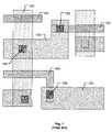
- FIG. 1shows a typical CMOS transistor configuration, in accordance with the prior art.
- a preferred direction for an interconnect level (metal-1)is parallel to that for gate electrode (gate) wires, as seen for metal-1 wire 105 and gate wire 103 .
- Gate wire 103overlaps a diffusion shape 101 , forming a transistor with a source or drain (S/D) node that is connected to metal-1 wire 105 by a contact 106 .
- Wire 105requires a non-rectangular shape, i.e., a shape with a bend, to allow it to overlap a contact 102 which connects to a gate wire 107 .
- FIG. 1also shows a gate electrode wire 104 that requires a bend to overlap a gate contact 108 , which connects to a metal-1 wire 109 .
- the typical CMOS transistor configuration of FIG. 1illustrates a number of features that may increase manufacturing difficulty. For example, contacts for S/D and gate connections are not aligned, gate and metal wire widths are variable, spacing between wire shapes is variable, wire center lines are variably spaced apart, and a ratio of filled to non-filled space for gate and metal-1 levels is variable.
- These featuresmay cause parametric and defect yield loss in advanced semiconductor processes due to associated lithographic effects, CMP (chemical mechanical planarization) dishing, and/or other manufacturing imperfections. Therefore, it is of interest to define a semiconductor device layout methodology that accounts for layout characteristics which adversely affect manufacturability.
- a methodfor defining a layout for a portion of a given semiconductor chip level.
- the methodincludes an operation for defining a preferred routing direction for a given chip level.
- the methodalso includes an operation for identifying each contact level related to the given chip level, wherein each contact level includes at least one interfacing contact defined to physically connect with a structure corresponding to a layout shape to be placed in the given chip level.
- An operationis then performed to define a global placement grating (GPG) for the given chip level to include a set of parallel and evenly spaced virtual lines. At least one virtual line of the GPG is positioned to intersect each interfacing contact within each contact level related to the given chip level.
- GPGglobal placement grating
- a methodfor defining a layout for a portion of a given semiconductor chip level.
- the methodincludes an operation for defining a GPG for a given chip level.
- the GPGis defined by a set of parallel and evenly spaced virtual lines. All connection lines within the GPG are identified.
- a connection lineis a virtual line of the GPG that is spatially coincident with a virtual line of a related contact level.
- the methodalso includes an operation for defining a subgrating for the given chip level as a set of evenly spaced connection lines, such that a spacing between adjacent connection lines in the subgrating is at least as large as a minimum spacing required to support a common run length of layout shapes on the adjacent connection lines in the subgrating.
- the operation for defining the subgratingis repeated until each connection line within the GPG is associated with at least one subgrating.
- the layout for the given chip levelis then partitioned into a number of subgrating regions. Each subgrating region is defined as a contiguous area within the layout for the given chip level. Subgratings are allocated to the number of subgrating regions such that only one subgrating is allocated to any one subgrating region.
- the methodfurther includes an operation for placing functional layout shapes for the given chip level in alignment to the subgratings allocated to the subgrating regions. Following placement of the functional layout shapes, a non-standard spacing is identified within the layout of the given chip level.
- the methodincludes an operation for resolving the non-standard spacing so as to ensure manufacturability of structures corresponding to the functional layout shapes.
- FIG. 1shows a typical CMOS transistor configuration, in accordance with the prior art
- FIG. 2shows a portion of a layout for a given chip level in which a GPG is defined and in which linear layout shapes are placed in alignment with the GPG, in accordance with one embodiment of the present invention
- FIG. 3Ashows an example in which a subgrating pitch results in a ratio of side-to-side spacing to layout shape width that is too large to maintain sufficient shape density for proper manufacturing
- FIG. 3Bshows a modification of the layout of FIG. 3A in which a subresolution shape is used to mitigate the unacceptably large side-to-side spacing to width ratio, in accordance with one embodiment of the present invention
- FIG. 4shows an example layout in which a GPG is used to place layout shapes for gate electrode wires, interconnect wires, diffusion contacts, and gate contacts, in accordance with one embodiment of the present invention
- FIG. 5shows an extension of the exemplary layout of FIG. 4 in which a number of subgrating regions are defined in various chip levels, in accordance with one embodiment of the present invention
- FIG. 6shows an example layout that illustrates subgrating use among different vertically stacked chip levels, in accordance with one embodiment of the present invention
- FIG. 7shows an example layout in which a multi-level orthogonally routed connection is used to connect wires in a same chip level that cannot have a common run length, in accordance with one embodiment of the present invention
- FIG. 8shows another example layout in which a multi-level orthogonally routed connection is used to connect wires in a same chip level that cannot have a common run length, in accordance with one embodiment of the present invention
- FIG. 9Bshows a layout shape stretching technique for mitigating a non-standard spacing introduced at subgrating region borders that lie parallel to the routing direction, in accordance with one embodiment of the present invention
- FIG. 10Ashows an example layout that illustrates the occurrence of a non-standard spacing at an interface between adjacent subgrating regions, when the layout shape stretching technique of FIG. 9B is blocked, in accordance with one embodiment of the present invention
- FIG. 10Billustrates use of a subresolution shape to mitigate a non-standard spacing at an interface between adjacent subgrating regions, when the layout shape stretching technique of FIG. 9B is blocked, in accordance with one embodiment of the present invention
- FIG. 11shows an exemplary layout in which a layout shape is stretched to overlap multiple contacts and/or vias, in accordance with one embodiment of the present invention
- FIG. 12shows another example in which layout shapes are stretched to overlap multiple contacts and/or vias, in accordance with one embodiment of the present invention
- FIG. 13shows an example in which layout shapes are extended relative to a contact and/or via so as to accommodate design requirements, in accordance with one embodiment of the present invention
- FIG. 14shows a flowchart of a method for defining a layout for a portion of a given semiconductor chip level, in accordance with one embodiment of the present invention
- FIG. 15Ashows a flowchart of a method for defining a layout for a portion of a given semiconductor chip level, in accordance with one embodiment of the present invention
- FIG. 15Bshows an expanded view of operation 1509 of FIG. 15A , in accordance with one embodiment of the present invention
- FIG. 15Cshows an extension of the method of FIGS. 15A-15B , in accordance with various embodiments of the present invention.
- FIG. 16shows a flowchart of a method for defining a layout for a portion of a given semiconductor chip level, in accordance with one embodiment of the present invention.
- a global placement gratingis defined by a set of parallel and evenly spaced virtual lines extending across a semiconductor chip (“chip” hereafter) level.
- the even, i.e., equal, perpendicular spacing between adjacent virtual lines of a GPGis referred to at the GPG pitch (GPGP).
- GPGPGPG pitch
- Layout shapes within a portion of a given chip levelcan be placed in accordance with the GPG of the given chip level. For example, layout shapes within a portion of a given chip level may be centered upon or in some way indexed to virtual lines of the GPG of the given chip level.
- the virtual lines of the GPG of a given chip levelare oriented to extend in a preferred routing direction of the given chip level, wherein the preferred routing direction corresponds to a direction in which layout shapes are defined to extend.
- the layout shapes placed in accordance with the GPGare defined as linear layout shapes.
- Each linear layout shapehas a substantially rectangular cross-section when viewed in an as-drawn state.
- the linear layout shapedoes allow for small deviations from the rectangular cross-section.
- a linear layout shapemay include one or more expanded regions along its rectangular cross-section length so as to accommodate contact placements and connections thereto.
- strict adherence to a substantially rectangular cross-sectionmay be specified for the linear layout shapes. It should be understood that a degree of rectangularity of the linear layout shapes can vary between embodiments, depending on the requirements for design and layout of a particular embodiment.
- each linear layout shape placed in a portion of a given chip levelis placed such that a length of its substantially rectangular cross-section is parallel with the GPG of the given chip level. Therefore, in this embodiment, the linear layout shapes extend in the preferred routing direction of the given chip level which is parallel to the virtual lines of the GPG.
- each linear layout shapeis initially placed in a centered manner such that its centerline extending in the preferred routing direction is substantially centered upon a virtual line of the GPG. It should be understood, however, that following initial placement of a given layout shape in the centered manner, a width of the given layout shape may be adjusted, or the given layout shape may be stretched in its width direction, such that a final version of the given layout shape is no longer centered upon a virtual line of the GPG.
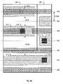
- FIG. 2shows a portion of a layout for a given chip level in which a GPG is defined and in which linear layout shapes are placed in alignment with the GPG, in accordance with one embodiment of the present invention.
- the GPG of FIG. 2is defined by virtual lines 200 - 209 , with adjacent virtual lines evenly spaced at the GPG pitch (GPGP).
- the virtual lines 200 - 209 of the GPGextend in the preferred routing direction of the given chip level.
- FIG. 2depicts layout shapes as shaded rectangular shapes.
- the layout shapes within the portion of the given chip levelare defined as linear layout shapes and are placed so as to be substantially centered upon a virtual line of the GPG.
- FIG. 2further illustrates concepts of the present invention referred to as subgrating and subgrating regions.
- a subgratingis defined as a set of evenly spaced GPG lines having a subgrating pitch that is an integer multiple of the GPG pitch.
- a subgrating regionis defined as a layout area of a portion of a given chip level within which layout shapes are placed according to a single subgrating.
- a subgratingis defined to accommodate a common run length of layout shapes having a specified uniform width, wherein the common run length refers to side-by-side existence of layout shapes on adjacent subgrating virtual lines.
- FIG. 2shows by way of example five separate subgrating regions 220 - 224 , where a periphery of each subgrating region 220 - 224 is delineated by bold solid lines.
- Each of subgrating regions 220 - 224is associated with a particular subgrating.
- the subgrating within each subgrating region 220 - 224is delineated by bold dashed lines.
- the subgratings for each of subgrating regions 220 and 224include each virtual line of the GPG (GPG virtual lines 200 - 206 for subgrating region 220 , and GPG virtual lines 207 - 209 for subgrating region 224 ).
- the subgrating for subgrating region 221includes every other even numbered virtual line of the GPG (GPG virtual lines 200 , 202 , 204 , 206 ), such that the corresponding subgrating pitch is 2*GPGP.
- the subgrating for subgrating region 222includes every other odd numbered virtual line of the GPG (GPG virtual lines 201 , 203 , 205 , 207 , 209 ), such that the corresponding subgrating pitch is 2*GPGP.
- the subgrating for subgrating region 223includes every third virtual line of the GPG, (GPG virtual lines 201 and 204 ), such that the corresponding subgrating pitch is 3*GPGP.
- linear layout shapesare initially placed in a centered manner on the subgrating of the subgrating region in which the linear layout shape is placed.
- layout shapes of uniform width placed in accordance with the same subgratingcan have a common run length.
- layout shapes that are placed on the same virtual line of the GPG in adjacent subgrating regionsmay, if necessary, be extended through the interface between the adjacent subgrating regions so as to combine and form single contiguous layout shape that spans the interface between the adjacent subgrating regions.
- FIG. 2shows layout shapes 250 A and 250 B extending through the interface between adjacent subgrating regions 222 and 224 so as to form a single layout shape 250 .
- a subgrating regionis defined as a contiguous area within a layout of a portion of a given chip level in which layout shapes are aligned to a common subgrating. It should also be understood that a subgrating region can be defined to have an arbitrary shape. However, in one embodiment, an effort is made to define subgrating regions such that a minimal number of boundary segments are used to define a periphery of each subgrating region. Also, in one embodiment, when possible, layout shapes having related functions are grouped together within a subgrating region so as to maximize subgrating region area and minimize the number of boundary segments between adjacent subgrating regions. Moreover, it is likely that connection points utilizing the same subgrating will have related or identical functions. Also, in one embodiment, fill shapes neighboring a given subgrating region are placed in accordance with the given subgrating region so as to further maximize the area of the given subgrating region.
- FIG. 3Ashows an example in which a subgrating pitch (SGP) results in a ratio of side-to-side spacing (S 1 ) to layout shape width (W) that is too large to maintain sufficient shape density for proper manufacturing.
- SGPsubgrating pitch
- FIG. 3Bshows a modification of the layout of FIG. 3A in which a subresolution shape 301 is used to mitigate the unacceptably large ratio (S 1 /W), in accordance with one embodiment of the present invention.
- the subresolution shape 301is defined to have a width (SRW) that is small enough to ensure that subresolution shape 301 will not be manufactured.
- the subresolution shape 301is placed such that a side-to-side spacing (S 2 ) with its neighboring layout shapes is optimized for manufacturability of the neighboring layout shapes.
- SRWwidth
- SLlength
- the presence of the subresolution shape 301will serve to enhance manufacturability of its neighboring layout shapes during a lithographic manufacturing process. It should be understood, however, that subresolution shapes are not intended to be manufactured and should not be placed or sized to cause their manufacture.
- the likelihood of subresolution shape being manufacturedcan be dependent upon a layout shape density in its surrounding neighborhood. Therefore, the placement and sizing of a given subresolution shape should consider the layout shape density around the given subresolution shape.
- a subresolution shapecan be placed within a subgrating region without regard to the corresponding subgrating for the purpose of enhancing manufacturability of layout shapes within the subgrating region.
- a subresolution shapecan be placed within a subgrating region in accordance with the corresponding subgrating for the purpose of enhancing manufacturability of layout shapes within the subgrating region.
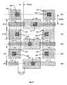
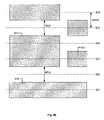
- FIG. 4shows an example layout in which a GPG is used to place layout shapes for gate electrode wires (“gates” hereafter), interconnect wires, diffusion contacts, and gate contacts, in accordance with one embodiment of the present invention.
- the GPGis defined by virtual lines 401 - 406 evenly spaced at GPG pitch (GPGP).
- Gate wires 410are placed according to a subgrating SG-A within the gate chip level that includes every other even numbered virtual line of the GPG (GPG virtual lines 402 , 404 , 406 ), such that the corresponding subgrating pitch is 2*GPGP.
- Interconnect wires 420are also placed according to the subgrating SG-A within a given interconnect chip level that includes every other even numbered virtual line of the GPG (GPG virtual lines 402 , 404 , 406 ).
- Interconnect wires 430are placed according to a subgrating SG-B within the given interconnect chip level that includes every other odd numbered virtual line of the GPG (GPG virtual lines 401 , 403 , 405 ), such that the corresponding subgrating pitch is 2*GPGP.
- Diffusion contacts 440i.e., source/drain contacts, are also placed according to the subgrating SG-B within the diffusion contact chip level that includes every other odd numbered virtual line of the GPG (GPG virtual lines 401 , 403 , 405 ).
- Gate contacts 450are placed according to the subgrating SG-A within the gate contact chip level that includes every other even numbered virtual line of the GPG (GPG virtual lines 402 , 404 , 406 ).
- layout shapes and subgratings within a portion of a given chip levelare defined to enable use of substantially uniform layout shapes widths, substantially uniform layout shape side-to-side spacings, and substantially uniform layout shape end-to-end spacings.
- the embodiment of FIG. 4shows use of a substantially uniform interconnect wire layout shape width (M 1 W) within the illustrated portion of the interconnect chip level.
- FIG. 4shows use of a substantially uniform interconnect layout shape side-to-side spacing (M 1 S) within the illustrated portion of the interconnect chip level.
- FIG. 4shows use of a substantially uniform interconnect layout shape end-to-end spacing (M 1 LES) within the illustrated portion of the interconnect chip level.
- FIG. 4shows use of a substantially uniform gate wire layout shape width (GW) within the illustrated portion of the gate chip level. Also, FIG. 4 shows use of a substantially uniform gate layout shape side-to-side spacing (GS) within the illustrated portion of the gate chip level. Also, FIG. 4 shows use of a substantially uniform gate layout shape end-to-end spacing (GLES) within the illustrated portion of the gate chip level.
- GWgate wire layout shape width
- GSsubstantially uniform gate layout shape side-to-side spacing
- GLESsubstantially uniform gate layout shape end-to-end spacing
- extension of a layout shape size through stretching of one or more of the layout shape's edgescan be used to achieve the substantially constant layout shape widths, side-to-side spacings, and end-to-end spacings.
- manufacturing benefitsmay be achieved by using substantially constant layout shape widths, side-to-side spacings, and end-to-end spacings
- use of GPGs, subgratings, and subgrating regionsdoes not require use of substantially constant layout shape widths, side-to-side spacings, and end-to-end spacings.
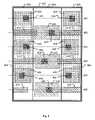
- FIG. 5shows an extension of the exemplary layout of FIG. 4 in which a number of subgrating regions are defined in various chip levels, in accordance with one embodiment of the present invention.
- a diffusion level of the exemplary layoutincludes diffusion regions 502 and 504 .
- a gate level of the exemplary layoutincludes the gate wire layout shapes 410 .
- a single subgrating region 507is defined for the gate level, with the subgrating SG-A allocated thereto.
- Three subgrating regions 501 , 503 , 505are defined for each of the diffusion contact level, gate contact level, and interconnect level with the subgratings SG-B, SG-A, SG-B allocated thereto, respectively. Therefore, each of the chip levels of the exemplary layout of FIG. 5 is partitioned into a number of subgrating regions, wherein each of these subgrating regions is defined as a contiguous area within the layout.
- FIG. 5also illustrates how layout shapes of related function can be placed together within a common subgrating region.
- diffusion contacts 440 and their associated interconnect wires 430are placed together in each of subgrating regions 501 and 505 in accordance with subgrating SG-B.
- gate contacts 450 and their associated interconnect wires 420are placed together in subgrating region 503 in accordance with subgrating SG-A.
- the gate wires 410are placed in subgrating region 507 in accordance with subgrating SG-A.
- a layout shape in one subgrating region of a given chip levelcan connect with another layout shape in an adjacent subgrating region of the given level when the two layout shapes are placed along the same virtual line of the GPG, thereby forming a larger shape that traverses across the interface between the adjacent subgrating regions.
- layout shapes 250 A and 250 B of FIG. 2combining to form layout shape 250 . Therefore, a layout shape can be defined to cross from one subgrating region to an adjacent subgrating region in a given level when the different subgratings in the adjacent subgrating regions align to a common GPG virtual line.
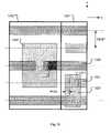
- FIG. 6shows an example layout that illustrates subgrating use among different vertically stacked chip levels, in accordance with one embodiment of the present invention.
- a metal-3 subgrating region 620includes vias 630 that connect to metal-2 wires 631 centered on horizontal GPG virtual line 650 .
- the vias 630 and metal-3 wires 632 that overlap themare centered on odd numbered vertical GPG virtual lines 611 , 613 , 615 , respectively, and have a horizontal pitch M 3 P 2 that is twice the vertical GPG pitch GPG 2 .
- vias 633 that connect to metal-2 wires 634are centered on horizontal GPG virtual line 651 , and the metal-3 wires 635 that overlap them are centered on even numbered vertical GPG virtual lines 610 , 612 , 614 , respectively, and have a horizontal pitch M 3 P 1 that is twice the vertical GPG pitch GPG 2 .
- FIG. 7shows an example layout in which a multi-level orthogonally routed connection is used to connect wires in a same chip level that cannot have a common run length, in accordance with one embodiment of the present invention.
- Parallel metal-1 layout shapes 702 , 701 , 700are centered on adjacent GPG virtual lines 740 , 741 , 742 , respectively, and have insufficient clearance to run side-by-side, i.e., to have a common run length. Therefore, the metal-1 layout shapes 700 , 701 , 702 cannot traverse the boundary between the adjacent subgrating regions 760 and 761 , and therefore cannot make a physical connection to each other within their chip level.
- One solutionis to use multiple chip levels with orthogonal routing directions to make the required connections.
- a diffusion shape 704is connected to gate wire 720 by connecting through each of diffusion contact 710 , metal-1 wire 701 , via 730 , metal-2 wire 740 , via 750 , metal-3 wire 770 , via 751 , metal-2 wire 741 , via 731 , metal-1 wire 702 , and contact 711 .
- This multiple chip level orthogonal routing connection solutioncan be generalized to form connections when layout shapes on a given level cannot traverse a subgrating region boundary that crosses their routing direction, i.e., when layout shapes on a given level cannot have a common run length.
- FIG. 8shows another example layout in which a multi-level orthogonally routed connection is used to connect wires in a same chip level that cannot have a common run length, in accordance with one embodiment of the present invention.
- Parallel metal-3 wires 800 - 803 centered on adjacent GPG lines 870 - 873cannot traverse the boundary 880 between metal-3 subgrating regions 820 and 821 . Therefore, due to the boundary 880 , a direct connection cannot be made between metal-3 wires 801 and 802 .
- FIG. 8also shows that wires on different levels with identical routing directions such as metal-1 wires 860 - 862 and metal-3 wires 800 - 803 may be centered on different GPGs such as the GPG with pitch GRM 3 for metal-3 and the GPG with pitch GRM 1 for metal-1.
- the GPG and subgrating region techniques described abovecan be used to enforce the following layout shape pattern regularity conventions that are beneficial to manufacturing: 1) layout shapes are rectangular, i.e., linear-shaped, 2) wire layout shape pitch is substantially constant in the direction orthogonal to routing, 3) contact layout shape pitch is substantially constant in the direction orthogonal to routing, 4) wire layout shape width is substantially constant, 5) wire layout shape side-to-side spacing is substantially constant, 6) wire layout shape end-to-end spacing is substantially constant, and 7) overall layout shape density is as uniform as possible.
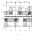
- FIG. 9Ashows an example layout that illustrates the occurrence of a non-standard spacing at an interface between adjacent subgrating regions, in accordance with one embodiment of the present invention.
- a metal-1 subgrating region 900that includes gate contacts 940 centered on even numbered GPG lines 924 , 926 , and a metal-1 subgrating region 901 that includes diffusion contacts 950 centered on odd GPG lines 921 , 923 .
- the metal-1 subgrating region 901borders the metal-1 subgrating region 900 both vertically and horizontally. This introduces a non-standard spacing, M 1 S 2 , straddling the horizontal subgrating regional border located between the metal-1 wires 910 and 912 .
- FIG. 9Bshows a layout shape stretching technique for mitigating a non-standard spacing introduced at subgrating region borders that lie parallel to the routing direction, in accordance with one embodiment of the present invention.
- the layout of FIG. 9Bis a modified version of the metal-1 layout of FIG. 9A .
- the edge of metal-1 wire 910 that faces the large gapis stretched until it is co-linear with the edge of a metal-1 wire 911 , which faces the same gap but is centered on an alternate grating line 923 .
- wire spaces M 1 Sare made constant, but the metal-1 wire 910 has non-standard width and is no longer centered on a GPG line.
- the stretching of the metal-1 wire 910 in favor of constant spacingprovides an overall improvement in manufacturability.
- FIG. 10Ashows an example layout that illustrates the occurrence of a non-standard spacing at an interface between adjacent subgrating regions, when the layout shape stretching technique of FIG. 9B is blocked, in accordance with one embodiment of the present invention.
- layout shape 1010 in subgrating region 1000runs parallel to a layout shape 1012 in subgrating region 1001 , wherein layout shapes 1010 and 1012 are aligned to different subgratings.
- the non-standard gap M 1 S 2extends along the common run length CRL of layout shapes 1010 and 1012 .
- the layout shape 1010cannot be stretched toward the layout shape 1012 to reduce M 1 S 2 because it is blocked by another layout shape 1013 in the same subgrating region 1000 .
- use of the constant GPGP value and the single layout shape width M 1 Wserves to limit the number of non-standard gap values to one, i.e., to the M 1 S 2 value. Therefore, through specification of a constant GPGP value and of a limited number of layout shape widths it is possible to optimize manufacturing processes to account for a controlled number of non-standard spacings that may occur in the layout. In contrast, it should be appreciated that such manufacturing process optimization is not feasible when an uncontrolled number of non-standard layout shape spacings may occur in a given layout.
- FIG. 10Billustrates use of a subresolution shape to mitigate a non-standard spacing at an interface between adjacent subgrating regions, as an alternative to the layout shape stretching technique of FIG. 9B is blocked, in accordance with one embodiment of the present invention.
- the layout of FIG. 10Bis a modified version of the layout of FIG. 10A .
- a sub-resolution layout shape 1014is placed within the area corresponding to the non-standard spacing.
- a width (SRW) of the subresolution layout shape 1014should be small enough to ensure that the subresolution layout shape 1014 is not manufactured.
- FIG. 11shows an exemplary layout in which a layout shape is stretched to overlap multiple contacts and/or vias, in accordance with one embodiment of the present invention.
- a linear layout shape of a wirecan be stretched orthogonally to its preferred routing direction so that it overlaps multiple contacts and/or vias.
- FIG. 11shows a metal-1 wire 1110 having a preferred horizontal routing direction, i.e., preferred x-direction of routing.
- the metal-1 wire 1110is placed in a subgrating region 1100 that is defined adjacent to a subgrating region 1103 .
- the metal-1 wire 1110needs to connect to each of contacts 1120 and 1121 .
- the metal-1 wire 1110may have been initially placed in a centered manner on a GPG virtual line, the metal-1 wire 1110 is stretched orthogonal to its preferred routing direction, i.e., is stretched in the y-direction, so as to cover both of contacts 1120 and 1121 .
- the linear layout shape stretching techniqueexemplified by the metal-1 wire 1110 of FIG. 11 , can be generalized to facilitate connection of layout shapes within different chip levels, within different subgrating regions of a given chip level, or within a same subgrating region of a given chip level.
- FIG. 12shows another example in which layout shapes are stretched to overlap multiple contacts and/or vias, in accordance with one embodiment of the present invention.
- a metal-2 wire layout shape 1231is stretched in the x-direction, i.e., widened, such that both of its edges maintain a standard spacing M 2 S to adjacent wire layout shapes 1232 and 1233 , and such that it overlaps and connects with a via 1240 and a via 1241 .
- the metal-2 wire 1231serves to connect a metal-3 wire 1261 in a metal-3 subgrating region 1270 to a metal-3 wire 1262 in a metal-3 subgrating region 1271 .
- a metal-2 wire layout shape 1230is similarly widened to overlap and connect with a via 1250 and a via 1242 , which are respectively connected to a metal-1 wire 1220 and a metal-3 wire 1260 .
- FIG. 13shows an example in which layout shapes are extended relative to a contact and/or via so as to accommodate design requirements, in accordance with one embodiment of the present invention.
- Two adjacent subgrating regions 1300 and 1301are defined for a metal-1 chip level.
- a diffusion contact 1311is defined to connect a diffusion region 1323 to a metal-1 wire 1321 .
- the diffusion contact 1311is covered by the metal-1 wire 1321 layout shape.
- a horizontal extension M 1 OL of the metal-1 wire 1321 layout shape in the x-directionis provided to enable compliance with design rules.
- a gate contact 1310is defined to connect a gate wire 1322 to a metal-1 wire 1320 .
- the metal-1 wire 1320 layout shapecan be defined to minimally overlap the gate contact 1310 in the x-direction due to the significant overlap of the gate contact 1310 by the metal-1 wire 1320 layout shape in the y-direction.
- the following layout methodcan be used for chip levels that are to be routed according to a GPG that is defined by a pitch too small to allow for common run lengths of shapes placed on adjacent GPG virtual lines.
- subgratingsare defined.
- alternate GPG linesare used for alternate functions when defining the subgratings.
- layout shapesare organized according to subgrating regions.
- layout shapes that use the same set of GPG virtual linesare grouped together in subgrating regions.
- Multiple chip levelscan be utilized to make connections between layout shapes of a given chip level when required due to fragmentation of those layout shapes at subgrating region boundaries within the given chip level.
- layout shapescan be stretched, i.e., widened, so as to maintain substantially constant side-to-side spacing where necessary, such as at subgrating region boundaries that run parallel to the preferred routing direction.
- non-standard spaces between layout shapes at subgrating region boundariescan be accepted when those non-standard spaces are predictable and fixed.
- non-standard spaces between layout shapes at subgrating region boundariescan be partially filled using subresolution layout shapes.
- layout shapes neighboring non-standard spaces at subgrating region boundariescan be stretched so as to mitigate the non-standard spaces.
- a layout shapecan be stretched, i.e., widened, in the direction orthogonal to its preferred routing direction so as to allow for connection of multiple overlapping contacts and/or vias to the layout shape.
- a layout shapecan be stretched, i.e., widened, in the direction orthogonal to its preferred routing direction so as to allow for reduction of contact and/or via overlap/extension by the layout shape in the direction parallel to its preferred routing direction.
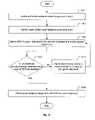
- FIG. 14shows a flowchart of a method for defining a layout for a portion of a given semiconductor chip level, in accordance with one embodiment of the present invention.
- the methodincludes an operation 1401 for defining a preferred routing direction for a given chip level.
- the methodalso includes an operation 1403 for identifying each contact level related to the given chip level, wherein such a related contact level includes at least one interfacing contact defined to physically connect with a structure corresponding to a layout shape to be placed in the given chip level.
- contact levels related to the given chip levelcan include a gate contact level, a diffusion contact level, a via level, or a combination thereof.
- the methodfurther includes an operation 1405 for defining a global placement grating (GPG) for the given chip level to include a set of parallel and evenly spaced virtual lines.
- GPGglobal placement grating
- the GPGis defined such that at least one virtual line of the GPG is positioned to intersect each interfacing contact within each contact level that is related to the given chip level, as identified in operation 1403 .
- An operation 1407is then performed to determine whether a perpendicular spacing between adjacent virtual lines of the GPG, i.e., GPG pitch, provides for enforcement of layout shape pattern regularity within the given chip level as necessary to ensure manufacturability of layout shapes within the given chip level.
- enforcement of layout shape pattern regularity within a given chip levelincludes one or more of 1) a substantially constant layout shape width as measured perpendicular to the preferred routing direction, 2) a substantially constant spacing between adjacently placed layout shapes as measured perpendicular to the preferred routing direction, and 3) a substantially constant spacing between ends of adjacently placed layout shapes as measured parallel to the preferred routing direction.
- An example of this embodimentis illustrated in FIG. 4 , as previously described.
- operation 1407determines that the perpendicular spacing between adjacent virtual lines of the global placement grating is not acceptable, the method proceeds with an operation 1411 for adjustment of the placement(s) of one or more contacts that interface with the given chip level. Then, the method reverts back to operation 1405 and proceeds as described above.
- the methodproceeds with an operation 1409 in which layout shapes are placed in alignment with the GPG for the given chip level.
- the layout shapes placed in alignment with the GPGare defined as linear layout shapes having a substantially rectangular cross-section when viewed in an as-drawn state.
- each linear layout shapeis placed such that a length of its substantially rectangular cross-section is parallel with the preferred routing direction.
- each linear layout shapeis initially placed such that its centerline extending in the preferred routing direction is substantially centered upon a virtual line of the GPG. It stood be understood, however, that after initial placement, some of the linear layout shapes may be stretched or otherwise modified to mitigate non-standard spacings within the layout so as to provide for sufficient layout shape pattern regularity as necessary to ensure manufacturability of layout shapes within the given chip level.
- FIG. 15Ashows a flowchart of a method for defining a layout for a portion of a given semiconductor chip level, in accordance with one embodiment of the present invention.
- the methodincludes an operation 1501 for defining a global placement grating (GPG) for a given chip level.
- the GPGis defined by a set of parallel and evenly spaced virtual lines.
- the methodalso includes an operation 1503 for identifying all connection lines within the GPG.
- a connection lineis a virtual line of the GPG that is spatially coincident with a virtual line of a related contact level.
- a related contact levelincludes at least one contact that is defined to physically connect with a structure corresponding to a layout shape placed within the given chip level.
- the virtual lines of any given related contact levelare defined as a set of parallel and equally spaced virtual lines to which contact layout shapes are aligned.
- the methodfurther includes an operation 1505 for defining a subgrating for the given chip level.
- a subgratingis defined as a set of evenly spaced connection lines, such that a spacing between adjacent connection lines in the subgrating is at least as large as a minimum spacing required to support a common run length of layout shapes on the adjacent connection lines in the subgrating.
- a common run length of two layout shapesoccurs where the two layout shapes are placed in a side-by-side manner on adjacent connection lines in the subgrating.
- defining a subgrating for a chip levelincludes associating the subgrating with a particular function to be performed by structures corresponding to layout shapes to be placed in accordance with the given subgrating. Also, in this embodiment, a perpendicular spacing between adjacent lines of the given subgrating is defined to accommodate placement of the layout shapes corresponding to the particular function.
- the methodproceeds with a decision operation 1507 for determining whether each connection line within the global placement grating is associated with at least one subgrating. If each connection line is not associated with at least one subgrating the method reverts back to proceed again with operation 1505 . However, if each connection line is associated with at least one subgrating, the method proceeds with operation 1509 for placing layout shapes in alignment with the defined subgratings, such that each layout shape is associated with any one subgrating.
- each layout shape of the given chip levelis placed in alignment with at least one subgrating for the given chip level and is defined as a linear layout shape having a substantially rectangular cross-section when viewed in an as-drawn state.
- Each linear layout shapeis placed such that its lengthwise centerline extends parallel to the virtual lines of the GPG.
- each linear layout shapeis initially placed such that its lengthwise centerline is substantially centered upon a line of its subgrating.
- FIG. 15Bshows an expanded view of operation 1509 , in accordance with one embodiment of the present invention.
- the layout for the given chip levelis partitioned into a number of subgrating regions. Each subgrating region is defined as a contiguous area within the layout for the given chip level.
- An operation 1513is performed to allocate subgratings to the number of subgrating regions, such that only one subgrating is allocated to any one subgrating region. It should be understood, however, that different subgrating regions can have different subgratings respectively allocated thereto.
- each of the number of subgrating regions within the given chip levelis defined such that a layout area of each subgrating region is made as large as possible while accommodating layout area requirements of every other subgrating region within the given chip level.
- the subgrating regions within the given chip levelare defined such that a minimal number of boundary segments are used to define a periphery of each subgrating region.
- the methodproceeds with an operation 1515 for placing a first set of layout shapes for the given chip level.
- Each layout shape of the first setis aligned to the subgrating for the subgrating region in which the layout shape is placed.
- each layout shape of the given chip levelis placed according to the following specifications: 1) the layout shape is placed in alignment with at least one subgrating for the given chip level and is defined as a linear layout shape having a substantially rectangular cross-section when viewed in an as-drawn state, 2) the layout shape is placed such that its lengthwise centerline extends parallel to the virtual lines of the GPG, 3) the layout shape is initially placed such that its lengthwise centerline is substantially centered upon a line of its subgrating.
- a particular linear layout shape of the given chip levelis stretched in its widthwise direction extending perpendicular to the virtual lines of the GPG, after the initial placement of the particular linear layout shape, such that a structure corresponding to the particular linear layout shape will physically connect with multiple contacts (i.e., contacts and/or vias) within one or more related contact levels.
- An example of thisis illustrated in FIG. 11 by the stretching of layout shape 1110 to cover and physically connect with contacts 1120 and 1121 .
- a particular linear layout shape of the given chip levelis stretched in its widthwise direction extending perpendicular to the virtual lines of the GPG, after the initial placement of the particular linear layout shape, such that a structure corresponding to the particular linear layout shape will sufficiently overlap one or more contacts (i.e., contacts and/or vias) within one or more related contact levels.
- An example of thisis illustrated in FIG. 13 by the stretching of layout shape 1320 to sufficiently overlap contact 1310 .
- some layout shapes in adjacent subgrating regions that are placed on a common virtual line of the GPGare extended through a boundary between the adjacent subgrating regions so as to form a single contiguous layout shape.
- two or more layout shapes respectively placed in adjacent subgrating regions of the given chip level and on different virtual lines of the GPGare electrically connected together by orthogonally routed structures that extend through multiple chip levels.
- the subgratings of the adjacent subgrating regionsmay not accommodate a common run length of the two or more layout shapes.
- FIG. 15Cshows an extension of the method of FIGS. 15A-15B , in accordance with various embodiments of the present invention.
- the methodproceeds from operation 1515 with an operation 1517 for identifying a blank space within the layout of the given chip level.
- the blank space in this embodimentis identified as a spatial area within the layout of the given chip level at which a non-standard spacing exists between layout shapes of the first set as placed in operation 1515 .
- the methodthen proceeds with an operation 1519 for identifying a subgrating associated with a neighboring layout shape of the first set relative to the blank space and proximate to the blank space.
- An operation 1521is then performed to define a second set of layout shapes for the given chip level within the blank space.
- the second set of layout shapesare placed in alignment with the subgrating identified in operation 1519 .
- the second set of layout shapesare defined within the blank space so as to optimize manufacturability of the first set of layout shapes.
- operations 1517 through 1521are repeated until each blank space within the given chip level has been considered for placement of one or more layout shapes of the second set therein.
- the methodproceeds from operation 1515 with an operation 1525 for identifying a non-standard spacing within the layout of the given chip level at an interface between adjacent subgrating regions.
- the methodthen proceeds with an operation 1527 for identifying a layout shape adjacent to the non-standard spacing that can be stretched toward the interface between the adjacent subgrating regions.
- An operation 1529is then performed to stretch the layout shape identified in operation 1527 toward the interface between the adjacent subgrating regions so as to mitigate the non-standard spacing.
- the layout shape identified in operation 1527is stretched within its subgrating region so as to align with another layout shape present in the adjacent subgrating region.
- the layout shape identified in operation 1527is a linear layout shape and is stretched in its widthwise direction that extends perpendicular to the virtual lines of the GPG.
- the methodproceeds from operation 1515 with an operation 1531 for identifying a non-standard spacing within the layout of the given chip level at an interface between adjacent subgrating regions.
- the methodthen proceeds with an operation 1533 for identifying an inability to stretch a layout shape adjacent to the non-standard spacing toward the interface between the adjacent subgrating regions.
- An operation 1535is then performed to define a subresolution layout shape within a layout area of the given chip level corresponding to the non-standard spacing.
- the subresolution shapeis defined to reinforce manufacturability of the first set of layout shapes near the non-standard spacing, and so as to ensure that the subresolution layout shape is not manufactured.
- one or more non-standard spacingsare identified within the layout of the given chip level.
- a decisionis made to not mitigate the identified non-standard spacings.
- the identified non-standard spacingsmay be dealt with through optimization of one or more manufacturing processes without requiring modification of the layout of the given chip level.
- FIG. 16shows a flowchart of a method for defining a layout for a portion of a given semiconductor chip level, in accordance with one embodiment of the present invention.
- the methodincludes an operation 1601 for defining a global placement grating (GPG) for a given chip level, wherein the global placement grating is defined by a set of parallel and evenly spaced virtual lines.
- the methodalso includes an operation 1603 for identifying all connection lines within the GPG.
- a connection lineis a virtual line of the GPG that is spatially coincident with a virtual line of a related contact level.
- the methodfurther includes an operation 1605 for defining a subgrating for the given chip level as a set of evenly spaced connection lines, such that a spacing between adjacent connection lines in the subgrating is at least as large as a minimum spacing required to support a common run length of layout shapes on the adjacent connection lines in the subgrating.
- a decision operation 1607is provided to determine whether or not each connection line within the GPG is associated with at least one subgrating. If each connection line within the GPG is not associated with at least one subgrating, the method reverts back to operation 1605 . If each connection line within the GPG is associated with at least one subgrating, the method continues with an operation 1609 for partitioning the layout for the given chip level into a number of subgrating regions. Each subgrating region is defined as a contiguous area within the layout for the given chip level. An operation 1611 is then performed to allocate subgratings to the number of subgrating regions such that only one subgrating is allocated to any one subgrating region. It should be understood that different subgratings can be allocated to different subgrating regions, so long as no more than one subgrating is allocated to a given subgrating region in a given chip level.
- the methodcontinues with an operation 1613 for placing functional layout shapes for the given chip level in alignment to the subgratings allocated to the subgrating regions.
- the methodproceeds with an operation 1615 for identifying a non-standard spacing within the layout of the given chip level.
- identifying the non-standard spacing in operation 1615includes comparing a side-to-side spacing of functional layout shapes located adjacent to each subgrating region interface extending parallel to the virtual lines of the GPG with a standard side-to-side spacing between (or specified for) adjacent functional layout shapes within the given chip level.
- an operation 1617is then performed to resolve the non-standard spacing so as to optimize manufacturability of structures corresponding to the functional layout shapes.
- resolving the non-standard spacing in operation 1617can include either stretching a functional layout shape to reduce the non-standard spacing, or inserting a non-functional layout shape within the non-standard spacing, or inserting a subresolution shape within the non-standard spacing, or a combination thereof.
- operation 1617includes making a decision to not mitigate the identified non-standard spacing.
- the identified non-standard spacingmay be dealt with through adjustment of one or more manufacturing processes without requiring modification of the layout of the given chip level.
- each functional layout shape of the given chip levelis placed in alignment with at least one subgrating for the given chip level and is defined as a linear layout shape having a substantially rectangular cross-section when viewed in an as-drawn state. Also in this embodiment, each functional layout shape is placed such that its lengthwise centerline extends parallel to the virtual lines of the GPG. Also in this embodiment, each functional layout shape is initially placed (prior to operation 1617 ) such that its lengthwise centerline is substantially centered upon a line of its subgrating.
- the chip layouts generated by the methods disclosed hereincan be stored in a tangible form, such as in a digital format on a computer readable medium.
- the invention described hereincan be embodied as computer readable code on a computer readable medium.
- the computer readable mediumis any data storage device that can store data which can thereafter be read by a computer system. Examples of the computer readable medium include hard drives, network attached storage (NAS), read-only memory, random-access memory, CD-ROMs, CD-Rs, CD-RWs, magnetic tapes, and other optical and non-optical data storage devices.
- the computer readable mediumcan also be distributed over a network of coupled computer systems so that the computer readable code is stored and executed in a distributed fashion.
- the inventionalso relates to a device or an apparatus for performing these operations.
- the apparatusmay be specially constructed for the required purpose, such as a special purpose computer.
- the computercan also perform other processing, program execution or routines that are not part of the special purpose, while still being capable of operating for the special purpose.
- the operationsmay be processed by a general purpose computer selectively activated or configured by one or more computer programs stored in the computer memory, cache, or obtained over a network. When data is obtained over a network the data maybe processed by other computers on the network, e.g., a cloud of computing resources.
- the embodiments of the present inventioncan also be defined as a machine that transforms data from one state to another state.
- the datamay represent an article, that can be represented as an electronic signal and electronically manipulate data.
- the transformed datacan, in some cases, be visually depicted on a display, representing the physical object that results from the transformation of data.
- the transformed datacan be saved to storage generally, or in particular formats that enable the construction or depiction of a physical and tangible object.
- the manipulationcan be performed by a processor.
- the processorthus transforms the data from one thing to another.
- the methodscan be processed by one or more machines or processors that can be connected over a network. Each machine can transform data from one state or thing to another, and can also process data, save data to storage, transmit data over a network, display the result, or communicate the result to another machine.
Landscapes
- Engineering & Computer Science (AREA)
- Physics & Mathematics (AREA)
- Computer Hardware Design (AREA)
- Theoretical Computer Science (AREA)
- General Physics & Mathematics (AREA)
- Geometry (AREA)
- Evolutionary Computation (AREA)
- General Engineering & Computer Science (AREA)
- Power Engineering (AREA)
- Microelectronics & Electronic Packaging (AREA)
- Condensed Matter Physics & Semiconductors (AREA)
- Computer Networks & Wireless Communication (AREA)
- Architecture (AREA)
- Design And Manufacture Of Integrated Circuits (AREA)
- Semiconductor Integrated Circuits (AREA)
Abstract
Description
- This application claims priority under 35 U.S.C. 119(e) to U.S. Provisional Patent Application No. 61/024,980, filed Jan. 31, 2008, entitled “Enforcement of Semiconductor Structure Regularity for Localized Transistors and Interconnect.” The disclosure of the above-identified provisional patent application is incorporated herein by reference.
FIG. 1 shows a typical CMOS transistor configuration, in accordance with the prior art. In the example ofFIG. 1 , a preferred direction for an interconnect level (metal-1) is parallel to that for gate electrode (gate) wires, as seen for metal-1wire 105 andgate wire 103.Gate wire 103 overlaps adiffusion shape 101, forming a transistor with a source or drain (S/D) node that is connected to metal-1wire 105 by acontact 106. Wire105 requires a non-rectangular shape, i.e., a shape with a bend, to allow it to overlap acontact 102 which connects to agate wire 107.FIG. 1 also shows agate electrode wire 104 that requires a bend to overlap agate contact 108, which connects to a metal-1wire 109.- The typical CMOS transistor configuration of
FIG. 1 illustrates a number of features that may increase manufacturing difficulty. For example, contacts for S/D and gate connections are not aligned, gate and metal wire widths are variable, spacing between wire shapes is variable, wire center lines are variably spaced apart, and a ratio of filled to non-filled space for gate and metal-1 levels is variable. These features may cause parametric and defect yield loss in advanced semiconductor processes due to associated lithographic effects, CMP (chemical mechanical planarization) dishing, and/or other manufacturing imperfections. Therefore, it is of interest to define a semiconductor device layout methodology that accounts for layout characteristics which adversely affect manufacturability. - In one embodiment, a method is disclosed for defining a layout for a portion of a given semiconductor chip level. The method includes an operation for defining a preferred routing direction for a given chip level. The method also includes an operation for identifying each contact level related to the given chip level, wherein each contact level includes at least one interfacing contact defined to physically connect with a structure corresponding to a layout shape to be placed in the given chip level. An operation is then performed to define a global placement grating (GPG) for the given chip level to include a set of parallel and evenly spaced virtual lines. At least one virtual line of the GPG is positioned to intersect each interfacing contact within each contact level related to the given chip level. A determination is then made as to whether a perpendicular spacing between adjacent virtual lines of the GPG provides for enforcement of layout shape pattern regularity within the given chip level as necessary to ensure manufacturability of layout shapes within the given chip level. If it is determined that the perpendicular spacing between adjacent virtual lines of the GPG is acceptable, the method proceeds with placement of layout shapes in alignment with the GPG for the given chip level. However, if it is determined that the perpendicular spacing between adjacent virtual lines of the GPG is not acceptable, the method proceeds with an operation for adjusting placement of one or more interfacing contacts within one or more contact levels related to the given chip level. The method then reverts back to the operation for defining the GPG for the given chip level.
- In another embodiment, a method is disclosed for defining a layout for a portion of a given semiconductor chip level. In the method, a GPG is defined for a given chip level. The GPG is defined by a set of parallel and evenly spaced virtual lines. The method includes identifying all connection lines within the GPG. A connection line is a virtual line of the GPG that is spatially coincident with a virtual line of a related contact level. A subgrating is defined for the given chip level as a set of evenly spaced connection lines, such that a spacing between adjacent connection lines in the subgrating is at least as large as a minimum spacing required to support a common run length of layout shapes on the adjacent connection lines in the subgrating. Definition of subgratings is repeated until each connection line within the GPG is associated with at least one subgrating. The method further includes placement of layout shapes in alignment with the defined subgratings, such that each layout shape is associated with any one subgrating.
- In another embodiment, a method is disclosed for defining a layout for a portion of a given semiconductor chip level. The method includes an operation for defining a GPG for a given chip level. The GPG is defined by a set of parallel and evenly spaced virtual lines. All connection lines within the GPG are identified. A connection line is a virtual line of the GPG that is spatially coincident with a virtual line of a related contact level. The method also includes an operation for defining a subgrating for the given chip level as a set of evenly spaced connection lines, such that a spacing between adjacent connection lines in the subgrating is at least as large as a minimum spacing required to support a common run length of layout shapes on the adjacent connection lines in the subgrating. The operation for defining the subgrating is repeated until each connection line within the GPG is associated with at least one subgrating. The layout for the given chip level is then partitioned into a number of subgrating regions. Each subgrating region is defined as a contiguous area within the layout for the given chip level. Subgratings are allocated to the number of subgrating regions such that only one subgrating is allocated to any one subgrating region. The method further includes an operation for placing functional layout shapes for the given chip level in alignment to the subgratings allocated to the subgrating regions. Following placement of the functional layout shapes, a non-standard spacing is identified within the layout of the given chip level. The method includes an operation for resolving the non-standard spacing so as to ensure manufacturability of structures corresponding to the functional layout shapes.
- Other aspects and advantages of the invention will become more apparent from the following detailed description, taken in conjunction with the accompanying drawings, illustrating by way of example the present invention.
FIG. 1 shows a typical CMOS transistor configuration, in accordance with the prior art;FIG. 2 shows a portion of a layout for a given chip level in which a GPG is defined and in which linear layout shapes are placed in alignment with the GPG, in accordance with one embodiment of the present invention;FIG. 3A shows an example in which a subgrating pitch results in a ratio of side-to-side spacing to layout shape width that is too large to maintain sufficient shape density for proper manufacturing;FIG. 3B shows a modification of the layout ofFIG. 3A in which a subresolution shape is used to mitigate the unacceptably large side-to-side spacing to width ratio, in accordance with one embodiment of the present invention;FIG. 4 shows an example layout in which a GPG is used to place layout shapes for gate electrode wires, interconnect wires, diffusion contacts, and gate contacts, in accordance with one embodiment of the present invention;FIG. 5 shows an extension of the exemplary layout ofFIG. 4 in which a number of subgrating regions are defined in various chip levels, in accordance with one embodiment of the present invention;FIG. 6 shows an example layout that illustrates subgrating use among different vertically stacked chip levels, in accordance with one embodiment of the present invention;FIG. 7 shows an example layout in which a multi-level orthogonally routed connection is used to connect wires in a same chip level that cannot have a common run length, in accordance with one embodiment of the present invention;FIG. 8 shows another example layout in which a multi-level orthogonally routed connection is used to connect wires in a same chip level that cannot have a common run length, in accordance with one embodiment of the present invention;FIG. 9A shows an example layout that illustrates the occurrence of a non-standard spacing at an interface between adjacent subgrating regions, in accordance with one embodiment of the present invention;FIG. 9B shows a layout shape stretching technique for mitigating a non-standard spacing introduced at subgrating region borders that lie parallel to the routing direction, in accordance with one embodiment of the present invention;FIG. 10A shows an example layout that illustrates the occurrence of a non-standard spacing at an interface between adjacent subgrating regions, when the layout shape stretching technique ofFIG. 9B is blocked, in accordance with one embodiment of the present invention;FIG. 10B illustrates use of a subresolution shape to mitigate a non-standard spacing at an interface between adjacent subgrating regions, when the layout shape stretching technique ofFIG. 9B is blocked, in accordance with one embodiment of the present invention;FIG. 11 shows an exemplary layout in which a layout shape is stretched to overlap multiple contacts and/or vias, in accordance with one embodiment of the present invention;FIG. 12 shows another example in which layout shapes are stretched to overlap multiple contacts and/or vias, in accordance with one embodiment of the present invention;FIG. 13 shows an example in which layout shapes are extended relative to a contact and/or via so as to accommodate design requirements, in accordance with one embodiment of the present invention;FIG. 14 shows a flowchart of a method for defining a layout for a portion of a given semiconductor chip level, in accordance with one embodiment of the present invention;FIG. 15A shows a flowchart of a method for defining a layout for a portion of a given semiconductor chip level, in accordance with one embodiment of the present invention;FIG. 15B shows an expanded view ofoperation 1509 ofFIG. 15A , in accordance with one embodiment of the present invention;FIG. 15C shows an extension of the method ofFIGS. 15A-15B , in accordance with various embodiments of the present invention; andFIG. 16 shows a flowchart of a method for defining a layout for a portion of a given semiconductor chip level, in accordance with one embodiment of the present invention.- In the following description, numerous specific details are set forth in order to provide a thorough understanding of the present invention. It will be apparent, however, to one skilled in the art that the present invention may be practiced without some or all of these specific details. In other instances, well known process operations have not been described in detail in order not to unnecessarily obscure the present invention.
- Within the context of the present invention, a global placement grating (GPG) is defined by a set of parallel and evenly spaced virtual lines extending across a semiconductor chip (“chip” hereafter) level. The even, i.e., equal, perpendicular spacing between adjacent virtual lines of a GPG is referred to at the GPG pitch (GPGP). Layout shapes within a portion of a given chip level can be placed in accordance with the GPG of the given chip level. For example, layout shapes within a portion of a given chip level may be centered upon or in some way indexed to virtual lines of the GPG of the given chip level. Also, the virtual lines of the GPG of a given chip level are oriented to extend in a preferred routing direction of the given chip level, wherein the preferred routing direction corresponds to a direction in which layout shapes are defined to extend.
- In one embodiment, the layout shapes placed in accordance with the GPG are defined as linear layout shapes. Each linear layout shape has a substantially rectangular cross-section when viewed in an as-drawn state. In one embodiment, the linear layout shape does allow for small deviations from the rectangular cross-section. For example, a linear layout shape may include one or more expanded regions along its rectangular cross-section length so as to accommodate contact placements and connections thereto. In another embodiment, strict adherence to a substantially rectangular cross-section may be specified for the linear layout shapes. It should be understood that a degree of rectangularity of the linear layout shapes can vary between embodiments, depending on the requirements for design and layout of a particular embodiment. In one embodiment, each linear layout shape placed in a portion of a given chip level is placed such that a length of its substantially rectangular cross-section is parallel with the GPG of the given chip level. Therefore, in this embodiment, the linear layout shapes extend in the preferred routing direction of the given chip level which is parallel to the virtual lines of the GPG.
- Also, in one embodiment, each linear layout shape is initially placed in a centered manner such that its centerline extending in the preferred routing direction is substantially centered upon a virtual line of the GPG. It should be understood, however, that following initial placement of a given layout shape in the centered manner, a width of the given layout shape may be adjusted, or the given layout shape may be stretched in its width direction, such that a final version of the given layout shape is no longer centered upon a virtual line of the GPG.
FIG. 2 shows a portion of a layout for a given chip level in which a GPG is defined and in which linear layout shapes are placed in alignment with the GPG, in accordance with one embodiment of the present invention. The GPG ofFIG. 2 is defined by virtual lines200-209, with adjacent virtual lines evenly spaced at the GPG pitch (GPGP). The virtual lines200-209 of the GPG extend in the preferred routing direction of the given chip level.FIG. 2 depicts layout shapes as shaded rectangular shapes. The layout shapes within the portion of the given chip level are defined as linear layout shapes and are placed so as to be substantially centered upon a virtual line of the GPG.FIG. 2 further illustrates concepts of the present invention referred to as subgrating and subgrating regions. A subgrating is defined as a set of evenly spaced GPG lines having a subgrating pitch that is an integer multiple of the GPG pitch. A subgrating region is defined as a layout area of a portion of a given chip level within which layout shapes are placed according to a single subgrating. In one embodiment, a subgrating is defined to accommodate a common run length of layout shapes having a specified uniform width, wherein the common run length refers to side-by-side existence of layout shapes on adjacent subgrating virtual lines.FIG. 2 shows by way of example five separate subgrating regions220-224, where a periphery of each subgrating region220-224 is delineated by bold solid lines. Each of subgrating regions220-224 is associated with a particular subgrating. The subgrating within each subgrating region220-224 is delineated by bold dashed lines. The subgratings for each ofsubgrating regions subgrating region 220, and GPG virtual lines207-209 for subgrating region224). The subgrating forsubgrating region 221 includes every other even numbered virtual line of the GPG (GPGvirtual lines subgrating region 222 includes every other odd numbered virtual line of the GPG (GPGvirtual lines subgrating region 223 includes every third virtual line of the GPG, (GPGvirtual lines 201 and204), such that the corresponding subgrating pitch is 3*GPGP.- As shown in
FIG. 2 , linear layout shapes are initially placed in a centered manner on the subgrating of the subgrating region in which the linear layout shape is placed. Also, it should be appreciated from the example ofFIG. 2 that layout shapes of uniform width placed in accordance with the same subgrating can have a common run length. Also, layout shapes that are placed on the same virtual line of the GPG in adjacent subgrating regions may, if necessary, be extended through the interface between the adjacent subgrating regions so as to combine and form single contiguous layout shape that spans the interface between the adjacent subgrating regions. For example,FIG. 2 showslayout shapes subgrating regions single layout shape 250. - It should be understood that a subgrating region is defined as a contiguous area within a layout of a portion of a given chip level in which layout shapes are aligned to a common subgrating. It should also be understood that a subgrating region can be defined to have an arbitrary shape. However, in one embodiment, an effort is made to define subgrating regions such that a minimal number of boundary segments are used to define a periphery of each subgrating region. Also, in one embodiment, when possible, layout shapes having related functions are grouped together within a subgrating region so as to maximize subgrating region area and minimize the number of boundary segments between adjacent subgrating regions. Moreover, it is likely that connection points utilizing the same subgrating will have related or identical functions. Also, in one embodiment, fill shapes neighboring a given subgrating region are placed in accordance with the given subgrating region so as to further maximize the area of the given subgrating region.
- When layout shapes are placed according to a subgrating, a situation may arise in which the subgrating pitch and the layout shape width result in a side-to-side spacing between adjacently placed layout shapes that is too large to ensure proper manufacturability of the layout shapes.
FIG. 3A shows an example in which a subgrating pitch (SGP) results in a ratio of side-to-side spacing (S1) to layout shape width (W) that is too large to maintain sufficient shape density for proper manufacturing. FIG. 3B shows a modification of the layout ofFIG. 3A in which asubresolution shape 301 is used to mitigate the unacceptably large ratio (S1/W), in accordance with one embodiment of the present invention. Thesubresolution shape 301 is defined to have a width (SRW) that is small enough to ensure thatsubresolution shape 301 will not be manufactured. Also, thesubresolution shape 301 is placed such that a side-to-side spacing (S2) with its neighboring layout shapes is optimized for manufacturability of the neighboring layout shapes. Also, in some embodiments, because the width (SRW) of thesubresolution shape 301 primarily governs whether or not thesubresolution shape 301 will actually resolve, i.e., be manufactured, a length (SL) of thesubresolution shape 301 can be made as large as necessary without increasing a likelihood that thesubresolution shape 301 is inadvertently manufactured. The presence of thesubresolution shape 301 will serve to enhance manufacturability of its neighboring layout shapes during a lithographic manufacturing process. It should be understood, however, that subresolution shapes are not intended to be manufactured and should not be placed or sized to cause their manufacture. Moreover, the likelihood of subresolution shape being manufactured can be dependent upon a layout shape density in its surrounding neighborhood. Therefore, the placement and sizing of a given subresolution shape should consider the layout shape density around the given subresolution shape.- In one embodiment, a subresolution shape can be placed within a subgrating region without regard to the corresponding subgrating for the purpose of enhancing manufacturability of layout shapes within the subgrating region. In another embodiment, a subresolution shape can be placed within a subgrating region in accordance with the corresponding subgrating for the purpose of enhancing manufacturability of layout shapes within the subgrating region.
FIG. 4 shows an example layout in which a GPG is used to place layout shapes for gate electrode wires (“gates” hereafter), interconnect wires, diffusion contacts, and gate contacts, in accordance with one embodiment of the present invention. The GPG is defined by virtual lines401-406 evenly spaced at GPG pitch (GPGP).Gate wires 410 are placed according to a subgrating SG-A within the gate chip level that includes every other even numbered virtual line of the GPG (GPGvirtual lines Interconnect wires 420 are also placed according to the subgrating SG-A within a given interconnect chip level that includes every other even numbered virtual line of the GPG (GPGvirtual lines Interconnect wires 430 are placed according to a subgrating SG-B within the given interconnect chip level that includes every other odd numbered virtual line of the GPG (GPGvirtual lines Diffusion contacts 440, i.e., source/drain contacts, are also placed according to the subgrating SG-B within the diffusion contact chip level that includes every other odd numbered virtual line of the GPG (GPGvirtual lines Gate contacts 450 are placed according to the subgrating SG-A within the gate contact chip level that includes every other even numbered virtual line of the GPG (GPGvirtual lines - In one embodiment, layout shapes and subgratings within a portion of a given chip level are defined to enable use of substantially uniform layout shapes widths, substantially uniform layout shape side-to-side spacings, and substantially uniform layout shape end-to-end spacings. For example, the embodiment of
FIG. 4 shows use of a substantially uniform interconnect wire layout shape width (M1W) within the illustrated portion of the interconnect chip level. Also,FIG. 4 shows use of a substantially uniform interconnect layout shape side-to-side spacing (M1S) within the illustrated portion of the interconnect chip level. Also,FIG. 4 shows use of a substantially uniform interconnect layout shape end-to-end spacing (M1LES) within the illustrated portion of the interconnect chip level. - Additionally,
FIG. 4 shows use of a substantially uniform gate wire layout shape width (GW) within the illustrated portion of the gate chip level. Also,FIG. 4 shows use of a substantially uniform gate layout shape side-to-side spacing (GS) within the illustrated portion of the gate chip level. Also,FIG. 4 shows use of a substantially uniform gate layout shape end-to-end spacing (GLES) within the illustrated portion of the gate chip level. In various embodiments, extension of a layout shape size through stretching of one or more of the layout shape's edges can be used to achieve the substantially constant layout shape widths, side-to-side spacings, and end-to-end spacings. Moreover, although manufacturing benefits (such as in lithography processes) may be achieved by using substantially constant layout shape widths, side-to-side spacings, and end-to-end spacings, it should be understood that use of GPGs, subgratings, and subgrating regions does not require use of substantially constant layout shape widths, side-to-side spacings, and end-to-end spacings. FIG. 5 shows an extension of the exemplary layout ofFIG. 4 in which a number of subgrating regions are defined in various chip levels, in accordance with one embodiment of the present invention. A diffusion level of the exemplary layout includesdiffusion regions single subgrating region 507 is defined for the gate level, with the subgrating SG-A allocated thereto. Threesubgrating regions FIG. 5 is partitioned into a number of subgrating regions, wherein each of these subgrating regions is defined as a contiguous area within the layout.FIG. 5 also illustrates how layout shapes of related function can be placed together within a common subgrating region. For example,diffusion contacts 440 and their associatedinterconnect wires 430 are placed together in each ofsubgrating regions gate contacts 450 and their associatedinterconnect wires 420 are placed together insubgrating region 503 in accordance with subgrating SG-A. Thegate wires 410 are placed insubgrating region 507 in accordance with subgrating SG-A. Based on the example ofFIG. 5 , it should be appreciated that allocation of a properly defined subgrating to a given subgrating region provides for placement of layout shapes having a common run length within the given subgrating region.- A layout shape in one subgrating region of a given chip level can connect with another layout shape in an adjacent subgrating region of the given level when the two layout shapes are placed along the same virtual line of the GPG, thereby forming a larger shape that traverses across the interface between the adjacent subgrating regions. This is illustrated above with regard to
layout shapes FIG. 2 combining to formlayout shape 250. Therefore, a layout shape can be defined to cross from one subgrating region to an adjacent subgrating region in a given level when the different subgratings in the adjacent subgrating regions align to a common GPG virtual line. - The techniques described herein may be generalized to enable pattern regularity for any number of chip levels that are partitioned into subgrating regions.
FIG. 6 shows an example layout that illustrates subgrating use among different vertically stacked chip levels, in accordance with one embodiment of the present invention. As shown inFIG. 6 , a metal-3subgrating region 620 includesvias 630 that connect to metal-2wires 631 centered on horizontal GPGvirtual line 650. Thevias 630 and metal-3wires 632 that overlap them are centered on odd numbered vertical GPGvirtual lines subgrating region 621, vias633 that connect to metal-2wires 634 are centered on horizontal GPGvirtual line 651, and the metal-3wires 635 that overlap them are centered on even numbered vertical GPGvirtual lines FIG. 7 shows an example layout in which a multi-level orthogonally routed connection is used to connect wires in a same chip level that cannot have a common run length, in accordance with one embodiment of the present invention. Parallel metal-1 layout shapes702,701,700 are centered on adjacent GPGvirtual lines adjacent subgrating regions - One solution is to use multiple chip levels with orthogonal routing directions to make the required connections. For example, as shown in
FIG. 7 , adiffusion shape 704 is connected togate wire 720 by connecting through each ofdiffusion contact 710, metal-1wire 701, via730, metal-2wire 740, via750, metal-3wire 770, via751, metal-2wire 741, via731, metal-1 wire702, and contact711. This multiple chip level orthogonal routing connection solution can be generalized to form connections when layout shapes on a given level cannot traverse a subgrating region boundary that crosses their routing direction, i.e., when layout shapes on a given level cannot have a common run length. FIG. 8 shows another example layout in which a multi-level orthogonally routed connection is used to connect wires in a same chip level that cannot have a common run length, in accordance with one embodiment of the present invention. Parallel metal-3 wires800-803 centered on adjacent GPG lines870-873 cannot traverse theboundary 880 between metal-3subgrating regions boundary 880, a direct connection cannot be made between metal-3wires wires wire 840, via850, metal-1wire 860, via851, metal-2wire 841, and via831.FIG. 8 also shows that wires on different levels with identical routing directions such as metal-1 wires860-862 and metal-3 wires800-803 may be centered on different GPGs such as the GPG with pitch GRM3 for metal-3 and the GPG with pitch GRM1 for metal-1.- In one embodiment, the GPG and subgrating region techniques described above can be used to enforce the following layout shape pattern regularity conventions that are beneficial to manufacturing: 1) layout shapes are rectangular, i.e., linear-shaped, 2) wire layout shape pitch is substantially constant in the direction orthogonal to routing, 3) contact layout shape pitch is substantially constant in the direction orthogonal to routing, 4) wire layout shape width is substantially constant, 5) wire layout shape side-to-side spacing is substantially constant, 6) wire layout shape end-to-end spacing is substantially constant, and 7) overall layout shape density is as uniform as possible.
FIG. 9A shows an example layout that illustrates the occurrence of a non-standard spacing at an interface between adjacent subgrating regions, in accordance with one embodiment of the present invention. In the example ofFIG. 9A , a metal-1subgrating region 900 that includesgate contacts 940 centered on even numberedGPG lines subgrating region 901 that includesdiffusion contacts 950 centered onodd GPG lines subgrating region 901 borders the metal-1subgrating region 900 both vertically and horizontally. This introduces a non-standard spacing, M1S2, straddling the horizontal subgrating regional border located between the metal-1wires FIG. 9B shows a layout shape stretching technique for mitigating a non-standard spacing introduced at subgrating region borders that lie parallel to the routing direction, in accordance with one embodiment of the present invention. The layout ofFIG. 9B is a modified version of the metal-1 layout ofFIG. 9A . InFIG. 9B , the edge of metal-1wire 910 that faces the large gap is stretched until it is co-linear with the edge of a metal-1wire 911, which faces the same gap but is centered on an alternategrating line 923. By stretching the metal-1wire 910, wire spaces M1S are made constant, but the metal-1wire 910 has non-standard width and is no longer centered on a GPG line. However, the stretching of the metal-1wire 910 in favor of constant spacing provides an overall improvement in manufacturability.FIG. 10A shows an example layout that illustrates the occurrence of a non-standard spacing at an interface between adjacent subgrating regions, when the layout shape stretching technique ofFIG. 9B is blocked, in accordance with one embodiment of the present invention. InFIG. 10A ,layout shape 1010 insubgrating region 1000 runs parallel to alayout shape 1012 insubgrating region 1001, whereinlayout shapes layout shapes layout shape 1010 cannot be stretched toward thelayout shape 1012 to reduce M1S2 because it is blocked by anotherlayout shape 1013 in thesame subgrating region 1000.- Due to the application of a GPG and fixed layout shape widths, M1S2 is most likely limited to a fixed value. In the example of
FIG. 10A , M1S2=3*GPGP-M1W. More specifically, the fixed value for M1S2 applies to regions of the chip that share the same GPGP and M1W values. Thus, it should be appreciated that even when non-standard gaps, e.g., M1S2, cannot be mitigated through layout shape modification (such as layout shape stretching), specification of a constant GPGP value and of a limited number of layout shape widths, e.g., M1W, will serve to limit the corresponding number of non-standard gap values that may occur in the layout. For instance, in the example ofFIG. 10A , use of the constant GPGP value and the single layout shape width M1W serves to limit the number of non-standard gap values to one, i.e., to the M1S2 value. Therefore, through specification of a constant GPGP value and of a limited number of layout shape widths it is possible to optimize manufacturing processes to account for a controlled number of non-standard spacings that may occur in the layout. In contrast, it should be appreciated that such manufacturing process optimization is not feasible when an uncontrolled number of non-standard layout shape spacings may occur in a given layout. FIG. 10B illustrates use of a subresolution shape to mitigate a non-standard spacing at an interface between adjacent subgrating regions, as an alternative to the layout shape stretching technique ofFIG. 9B is blocked, in accordance with one embodiment of the present invention. The layout ofFIG. 10B is a modified version of the layout ofFIG. 10A . InFIG. 10B , asub-resolution layout shape 1014 is placed within the area corresponding to the non-standard spacing. As with the previous subresolution layout shape description ofFIG. 3B , a width (SRW) of thesubresolution layout shape 1014 should be small enough to ensure that thesubresolution layout shape 1014 is not manufactured. It should be appreciated that overall layout shape density and layout shape side-to-side spacing M1S can be made substantially uniform through use of this subresolution layout shape insertion technique. It should be understood, however, that in some embodiments the presence of a non-standard spacing at subgrating region boundaries is acceptable and does not require mitigation.FIG. 11 shows an exemplary layout in which a layout shape is stretched to overlap multiple contacts and/or vias, in accordance with one embodiment of the present invention. In one embodiment, a linear layout shape of a wire can be stretched orthogonally to its preferred routing direction so that it overlaps multiple contacts and/or vias. For example,FIG. 11 shows a metal-1 wire1110 having a preferred horizontal routing direction, i.e., preferred x-direction of routing. The metal-1 wire1110 is placed in asubgrating region 1100 that is defined adjacent to asubgrating region 1103. The metal-1 wire1110 needs to connect to each ofcontacts contacts FIG. 11 , can be generalized to facilitate connection of layout shapes within different chip levels, within different subgrating regions of a given chip level, or within a same subgrating region of a given chip level.FIG. 12 shows another example in which layout shapes are stretched to overlap multiple contacts and/or vias, in accordance with one embodiment of the present invention. InFIG. 12 , a metal-2wire layout shape 1231 is stretched in the x-direction, i.e., widened, such that both of its edges maintain a standard spacing M2S to adjacentwire layout shapes wire 1231 serves to connect a metal-3wire 1261 in a metal-3subgrating region 1270 to a metal-3wire 1262 in a metal-3subgrating region 1271. Also, a metal-2wire layout shape 1230 is similarly widened to overlap and connect with a via1250 and a via1242, which are respectively connected to a metal-1wire 1220 and a metal-3wire 1260.FIG. 13 shows an example in which layout shapes are extended relative to a contact and/or via so as to accommodate design requirements, in accordance with one embodiment of the present invention. Twoadjacent subgrating regions diffusion contact 1311 is defined to connect adiffusion region 1323 to a metal-1wire 1321. Thediffusion contact 1311 is covered by the metal-1wire 1321 layout shape. Given a lack of metal-1wire 1321 overlap of thecontact 1311 in the y-direction, a horizontal extension M1OL of the metal-1wire 1321 layout shape in the x-direction is provided to enable compliance with design rules. Also, agate contact 1310 is defined to connect agate wire 1322 to a metal-1wire 1320. The metal-1wire 1320 layout shape can be defined to minimally overlap thegate contact 1310 in the x-direction due to the significant overlap of thegate contact 1310 by the metal-1wire 1320 layout shape in the y-direction.- It should be understood that the manufacturability benefits of layout techniques described herein are preserved if dimensions referred to as substantially constant are allowed to vary slightly, so long as general layout pattern regularity is preserved. In one embodiment, the following layout method can be used for chip levels that are to be routed according to a GPG that is defined by a pitch too small to allow for common run lengths of shapes placed on adjacent GPG virtual lines. First, subgratings are defined. In one embodiment, alternate GPG lines are used for alternate functions when defining the subgratings. Then, layout shapes are organized according to subgrating regions. In one embodiment, layout shapes that use the same set of GPG virtual lines are grouped together in subgrating regions. Multiple chip levels can be utilized to make connections between layout shapes of a given chip level when required due to fragmentation of those layout shapes at subgrating region boundaries within the given chip level.
- Additionally, after initial layout shape placement, layout shapes can be stretched, i.e., widened, so as to maintain substantially constant side-to-side spacing where necessary, such as at subgrating region boundaries that run parallel to the preferred routing direction. In some instances, non-standard spaces between layout shapes at subgrating region boundaries can be accepted when those non-standard spaces are predictable and fixed. Also, in some instances, non-standard spaces between layout shapes at subgrating region boundaries can be partially filled using subresolution layout shapes. Moreover, in some instances, layout shapes neighboring non-standard spaces at subgrating region boundaries can be stretched so as to mitigate the non-standard spaces. Furthermore, a layout shape can be stretched, i.e., widened, in the direction orthogonal to its preferred routing direction so as to allow for connection of multiple overlapping contacts and/or vias to the layout shape. Also, a layout shape can be stretched, i.e., widened, in the direction orthogonal to its preferred routing direction so as to allow for reduction of contact and/or via overlap/extension by the layout shape in the direction parallel to its preferred routing direction.
FIG. 14 shows a flowchart of a method for defining a layout for a portion of a given semiconductor chip level, in accordance with one embodiment of the present invention. The method includes anoperation 1401 for defining a preferred routing direction for a given chip level. The method also includes anoperation 1403 for identifying each contact level related to the given chip level, wherein such a related contact level includes at least one interfacing contact defined to physically connect with a structure corresponding to a layout shape to be placed in the given chip level. In various embodiments, contact levels related to the given chip level can include a gate contact level, a diffusion contact level, a via level, or a combination thereof.- The method further includes an
operation 1405 for defining a global placement grating (GPG) for the given chip level to include a set of parallel and evenly spaced virtual lines. The GPG is defined such that at least one virtual line of the GPG is positioned to intersect each interfacing contact within each contact level that is related to the given chip level, as identified inoperation 1403. Anoperation 1407 is then performed to determine whether a perpendicular spacing between adjacent virtual lines of the GPG, i.e., GPG pitch, provides for enforcement of layout shape pattern regularity within the given chip level as necessary to ensure manufacturability of layout shapes within the given chip level. - It should be understood that what constitutes sufficient layout shape pattern regularity can be dependent upon many factors, such as a critical dimension of structures to be defined in the chip, a spacing between structures to be defined in the chip, and/or a function of structures to be defined in the chip, among others. Thus, it should be understood that what constitutes sufficient layout shape pattern regularity can vary from one design to another. In one particular embodiment, enforcement of layout shape pattern regularity within a given chip level includes one or more of 1) a substantially constant layout shape width as measured perpendicular to the preferred routing direction, 2) a substantially constant spacing between adjacently placed layout shapes as measured perpendicular to the preferred routing direction, and 3) a substantially constant spacing between ends of adjacently placed layout shapes as measured parallel to the preferred routing direction. An example of this embodiment is illustrated in
FIG. 4 , as previously described. - If
operation 1407 determines that the perpendicular spacing between adjacent virtual lines of the global placement grating is not acceptable, the method proceeds with anoperation 1411 for adjustment of the placement(s) of one or more contacts that interface with the given chip level. Then, the method reverts back tooperation 1405 and proceeds as described above. - If
operation 1407 determines that the perpendicular spacing between adjacent virtual lines of the global placement grating is acceptable, the method proceeds with anoperation 1409 in which layout shapes are placed in alignment with the GPG for the given chip level. In one embodiment, the layout shapes placed in alignment with the GPG are defined as linear layout shapes having a substantially rectangular cross-section when viewed in an as-drawn state. Also, in one embodiment, each linear layout shape is placed such that a length of its substantially rectangular cross-section is parallel with the preferred routing direction. Additionally, in one embodiment, each linear layout shape is initially placed such that its centerline extending in the preferred routing direction is substantially centered upon a virtual line of the GPG. It stood be understood, however, that after initial placement, some of the linear layout shapes may be stretched or otherwise modified to mitigate non-standard spacings within the layout so as to provide for sufficient layout shape pattern regularity as necessary to ensure manufacturability of layout shapes within the given chip level. FIG. 15A shows a flowchart of a method for defining a layout for a portion of a given semiconductor chip level, in accordance with one embodiment of the present invention. The method includes anoperation 1501 for defining a global placement grating (GPG) for a given chip level. The GPG is defined by a set of parallel and evenly spaced virtual lines. The method also includes anoperation 1503 for identifying all connection lines within the GPG. A connection line is a virtual line of the GPG that is spatially coincident with a virtual line of a related contact level. A related contact level includes at least one contact that is defined to physically connect with a structure corresponding to a layout shape placed within the given chip level. The virtual lines of any given related contact level are defined as a set of parallel and equally spaced virtual lines to which contact layout shapes are aligned.- The method further includes an
operation 1505 for defining a subgrating for the given chip level. A subgrating is defined as a set of evenly spaced connection lines, such that a spacing between adjacent connection lines in the subgrating is at least as large as a minimum spacing required to support a common run length of layout shapes on the adjacent connection lines in the subgrating. A common run length of two layout shapes occurs where the two layout shapes are placed in a side-by-side manner on adjacent connection lines in the subgrating. In one embodiment, defining a subgrating for a chip level includes associating the subgrating with a particular function to be performed by structures corresponding to layout shapes to be placed in accordance with the given subgrating. Also, in this embodiment, a perpendicular spacing between adjacent lines of the given subgrating is defined to accommodate placement of the layout shapes corresponding to the particular function. - Following
operation 1505, the method proceeds with adecision operation 1507 for determining whether each connection line within the global placement grating is associated with at least one subgrating. If each connection line is not associated with at least one subgrating the method reverts back to proceed again withoperation 1505. However, if each connection line is associated with at least one subgrating, the method proceeds withoperation 1509 for placing layout shapes in alignment with the defined subgratings, such that each layout shape is associated with any one subgrating. - In one embodiment, each layout shape of the given chip level is placed in alignment with at least one subgrating for the given chip level and is defined as a linear layout shape having a substantially rectangular cross-section when viewed in an as-drawn state. Each linear layout shape is placed such that its lengthwise centerline extends parallel to the virtual lines of the GPG. Also, each linear layout shape is initially placed such that its lengthwise centerline is substantially centered upon a line of its subgrating.
FIG. 15B shows an expanded view ofoperation 1509, in accordance with one embodiment of the present invention. In anoperation 1511, the layout for the given chip level is partitioned into a number of subgrating regions. Each subgrating region is defined as a contiguous area within the layout for the given chip level. Anoperation 1513 is performed to allocate subgratings to the number of subgrating regions, such that only one subgrating is allocated to any one subgrating region. It should be understood, however, that different subgrating regions can have different subgratings respectively allocated thereto. In one embodiment, each of the number of subgrating regions within the given chip level is defined such that a layout area of each subgrating region is made as large as possible while accommodating layout area requirements of every other subgrating region within the given chip level. Also in this embodiment, the subgrating regions within the given chip level are defined such that a minimal number of boundary segments are used to define a periphery of each subgrating region.- Once the subgrating regions are defined and have subgratings allocated thereto, the method proceeds with an
operation 1515 for placing a first set of layout shapes for the given chip level. Each layout shape of the first set is aligned to the subgrating for the subgrating region in which the layout shape is placed. In one embodiment, each layout shape of the given chip level is placed according to the following specifications: 1) the layout shape is placed in alignment with at least one subgrating for the given chip level and is defined as a linear layout shape having a substantially rectangular cross-section when viewed in an as-drawn state, 2) the layout shape is placed such that its lengthwise centerline extends parallel to the virtual lines of the GPG, 3) the layout shape is initially placed such that its lengthwise centerline is substantially centered upon a line of its subgrating. - In one augmentation of the above-described embodiment, a particular linear layout shape of the given chip level is stretched in its widthwise direction extending perpendicular to the virtual lines of the GPG, after the initial placement of the particular linear layout shape, such that a structure corresponding to the particular linear layout shape will physically connect with multiple contacts (i.e., contacts and/or vias) within one or more related contact levels. An example of this is illustrated in
FIG. 11 by the stretching of layout shape1110 to cover and physically connect withcontacts FIG. 13 by the stretching oflayout shape 1320 to sufficiently overlapcontact 1310. - Additionally, in one embodiment, some layout shapes in adjacent subgrating regions that are placed on a common virtual line of the GPG are extended through a boundary between the adjacent subgrating regions so as to form a single contiguous layout shape. In yet another embodiment, two or more layout shapes respectively placed in adjacent subgrating regions of the given chip level and on different virtual lines of the GPG are electrically connected together by orthogonally routed structures that extend through multiple chip levels. In this embodiment, the subgratings of the adjacent subgrating regions may not accommodate a common run length of the two or more layout shapes.
FIG. 15C shows an extension of the method ofFIGS. 15A-15B , in accordance with various embodiments of the present invention. In one embodiment, the method proceeds fromoperation 1515 with anoperation 1517 for identifying a blank space within the layout of the given chip level. The blank space in this embodiment is identified as a spatial area within the layout of the given chip level at which a non-standard spacing exists between layout shapes of the first set as placed inoperation 1515. The method then proceeds with anoperation 1519 for identifying a subgrating associated with a neighboring layout shape of the first set relative to the blank space and proximate to the blank space. Anoperation 1521 is then performed to define a second set of layout shapes for the given chip level within the blank space. The second set of layout shapes are placed in alignment with the subgrating identified inoperation 1519. The second set of layout shapes are defined within the blank space so as to optimize manufacturability of the first set of layout shapes. In one embodiment,operations 1517 through1521 are repeated until each blank space within the given chip level has been considered for placement of one or more layout shapes of the second set therein.- In another embodiment, the method proceeds from
operation 1515 with anoperation 1525 for identifying a non-standard spacing within the layout of the given chip level at an interface between adjacent subgrating regions. The method then proceeds with anoperation 1527 for identifying a layout shape adjacent to the non-standard spacing that can be stretched toward the interface between the adjacent subgrating regions. Anoperation 1529 is then performed to stretch the layout shape identified inoperation 1527 toward the interface between the adjacent subgrating regions so as to mitigate the non-standard spacing. In one embodiment, the layout shape identified inoperation 1527 is stretched within its subgrating region so as to align with another layout shape present in the adjacent subgrating region. In one embodiment the layout shape identified inoperation 1527 is a linear layout shape and is stretched in its widthwise direction that extends perpendicular to the virtual lines of the GPG. - In yet another embodiment, the method proceeds from
operation 1515 with anoperation 1531 for identifying a non-standard spacing within the layout of the given chip level at an interface between adjacent subgrating regions. The method then proceeds with anoperation 1533 for identifying an inability to stretch a layout shape adjacent to the non-standard spacing toward the interface between the adjacent subgrating regions. Anoperation 1535 is then performed to define a subresolution layout shape within a layout area of the given chip level corresponding to the non-standard spacing. The subresolution shape is defined to reinforce manufacturability of the first set of layout shapes near the non-standard spacing, and so as to ensure that the subresolution layout shape is not manufactured. - In yet another embodiment, following
operation 1515, one or more non-standard spacings are identified within the layout of the given chip level. In this embodiment, a decision is made to not mitigate the identified non-standard spacings. For example, the identified non-standard spacings may be dealt with through optimization of one or more manufacturing processes without requiring modification of the layout of the given chip level. FIG. 16 shows a flowchart of a method for defining a layout for a portion of a given semiconductor chip level, in accordance with one embodiment of the present invention. The method includes anoperation 1601 for defining a global placement grating (GPG) for a given chip level, wherein the global placement grating is defined by a set of parallel and evenly spaced virtual lines. The method also includes anoperation 1603 for identifying all connection lines within the GPG. A connection line is a virtual line of the GPG that is spatially coincident with a virtual line of a related contact level. The method further includes anoperation 1605 for defining a subgrating for the given chip level as a set of evenly spaced connection lines, such that a spacing between adjacent connection lines in the subgrating is at least as large as a minimum spacing required to support a common run length of layout shapes on the adjacent connection lines in the subgrating.- A
decision operation 1607 is provided to determine whether or not each connection line within the GPG is associated with at least one subgrating. If each connection line within the GPG is not associated with at least one subgrating, the method reverts back tooperation 1605. If each connection line within the GPG is associated with at least one subgrating, the method continues with anoperation 1609 for partitioning the layout for the given chip level into a number of subgrating regions. Each subgrating region is defined as a contiguous area within the layout for the given chip level. Anoperation 1611 is then performed to allocate subgratings to the number of subgrating regions such that only one subgrating is allocated to any one subgrating region. It should be understood that different subgratings can be allocated to different subgrating regions, so long as no more than one subgrating is allocated to a given subgrating region in a given chip level. - The method continues with an
operation 1613 for placing functional layout shapes for the given chip level in alignment to the subgratings allocated to the subgrating regions. Following placement of the functional layout shapes inoperation 1613, the method proceeds with anoperation 1615 for identifying a non-standard spacing within the layout of the given chip level. In one embodiment, identifying the non-standard spacing inoperation 1615 includes comparing a side-to-side spacing of functional layout shapes located adjacent to each subgrating region interface extending parallel to the virtual lines of the GPG with a standard side-to-side spacing between (or specified for) adjacent functional layout shapes within the given chip level. - In one embodiment, an
operation 1617 is then performed to resolve the non- standard spacing so as to optimize manufacturability of structures corresponding to the functional layout shapes. In various embodiments, resolving the non-standard spacing inoperation 1617 can include either stretching a functional layout shape to reduce the non-standard spacing, or inserting a non-functional layout shape within the non-standard spacing, or inserting a subresolution shape within the non-standard spacing, or a combination thereof. - In an alternative embodiment,
operation 1617 includes making a decision to not mitigate the identified non-standard spacing. For example, the identified non-standard spacing may be dealt with through adjustment of one or more manufacturing processes without requiring modification of the layout of the given chip level. - In one embodiment, each functional layout shape of the given chip level is placed in alignment with at least one subgrating for the given chip level and is defined as a linear layout shape having a substantially rectangular cross-section when viewed in an as-drawn state. Also in this embodiment, each functional layout shape is placed such that its lengthwise centerline extends parallel to the virtual lines of the GPG. Also in this embodiment, each functional layout shape is initially placed (prior to operation1617) such that its lengthwise centerline is substantially centered upon a line of its subgrating.
- It should be understood that the chip layouts generated by the methods disclosed herein can be stored in a tangible form, such as in a digital format on a computer readable medium. Also, the invention described herein can be embodied as computer readable code on a computer readable medium. The computer readable medium is any data storage device that can store data which can thereafter be read by a computer system. Examples of the computer readable medium include hard drives, network attached storage (NAS), read-only memory, random-access memory, CD-ROMs, CD-Rs, CD-RWs, magnetic tapes, and other optical and non-optical data storage devices. The computer readable medium can also be distributed over a network of coupled computer systems so that the computer readable code is stored and executed in a distributed fashion.
- Any of the operations described herein that form part of the invention are useful machine operations. The invention also relates to a device or an apparatus for performing these operations. The apparatus may be specially constructed for the required purpose, such as a special purpose computer. When defined as a special purpose computer, the computer can also perform other processing, program execution or routines that are not part of the special purpose, while still being capable of operating for the special purpose. Alternatively, the operations may be processed by a general purpose computer selectively activated or configured by one or more computer programs stored in the computer memory, cache, or obtained over a network. When data is obtained over a network the data maybe processed by other computers on the network, e.g., a cloud of computing resources.
- The embodiments of the present invention can also be defined as a machine that transforms data from one state to another state. The data may represent an article, that can be represented as an electronic signal and electronically manipulate data. The transformed data can, in some cases, be visually depicted on a display, representing the physical object that results from the transformation of data. The transformed data can be saved to storage generally, or in particular formats that enable the construction or depiction of a physical and tangible object. In some embodiments, the manipulation can be performed by a processor. In such an example, the processor thus transforms the data from one thing to another. Still further, the methods can be processed by one or more machines or processors that can be connected over a network. Each machine can transform data from one state or thing to another, and can also process data, save data to storage, transmit data over a network, display the result, or communicate the result to another machine.
- While this invention has been described in terms of several embodiments, it will be appreciated that those skilled in the art upon reading the preceding specifications and studying the drawings will realize various alterations, additions, permutations and equivalents thereof. Therefore, it is intended that the present invention includes all such alterations, additions, permutations, and equivalents as fall within the true spirit and scope of the invention.
Claims (34)
Priority Applications (5)
| Application Number | Priority Date | Filing Date | Title |
|---|---|---|---|
| US12/363,705US8453094B2 (en) | 2008-01-31 | 2009-01-30 | Enforcement of semiconductor structure regularity for localized transistors and interconnect |
| US13/897,307US8701071B2 (en) | 2008-01-31 | 2013-05-17 | Enforcement of semiconductor structure regularity for localized transistors and interconnect |
| US14/216,891US9202779B2 (en) | 2008-01-31 | 2014-03-17 | Enforcement of semiconductor structure regularity for localized transistors and interconnect |
| US14/949,761US9530734B2 (en) | 2008-01-31 | 2015-11-23 | Enforcement of semiconductor structure regularity for localized transistors and interconnect |
| US15/383,946US20170098602A1 (en) | 2008-01-31 | 2016-12-19 | Enforcement of Semiconductor Structure Regularity for Localized Transistors and Interconnect |
Applications Claiming Priority (2)
| Application Number | Priority Date | Filing Date | Title |
|---|---|---|---|
| US2498008P | 2008-01-31 | 2008-01-31 | |
| US12/363,705US8453094B2 (en) | 2008-01-31 | 2009-01-30 | Enforcement of semiconductor structure regularity for localized transistors and interconnect |
Related Child Applications (1)
| Application Number | Title | Priority Date | Filing Date |
|---|---|---|---|
| US13/897,307DivisionUS8701071B2 (en) | 2008-01-31 | 2013-05-17 | Enforcement of semiconductor structure regularity for localized transistors and interconnect |
Publications (2)
| Publication Number | Publication Date |
|---|---|
| US20090228857A1true US20090228857A1 (en) | 2009-09-10 |
| US8453094B2 US8453094B2 (en) | 2013-05-28 |
Family
ID=41054926
Family Applications (5)
| Application Number | Title | Priority Date | Filing Date |
|---|---|---|---|
| US12/363,705Expired - Fee RelatedUS8453094B2 (en) | 2008-01-31 | 2009-01-30 | Enforcement of semiconductor structure regularity for localized transistors and interconnect |
| US13/897,307Expired - Fee RelatedUS8701071B2 (en) | 2008-01-31 | 2013-05-17 | Enforcement of semiconductor structure regularity for localized transistors and interconnect |
| US14/216,891Expired - Fee RelatedUS9202779B2 (en) | 2008-01-31 | 2014-03-17 | Enforcement of semiconductor structure regularity for localized transistors and interconnect |
| US14/949,761Expired - Fee RelatedUS9530734B2 (en) | 2008-01-31 | 2015-11-23 | Enforcement of semiconductor structure regularity for localized transistors and interconnect |
| US15/383,946AbandonedUS20170098602A1 (en) | 2008-01-31 | 2016-12-19 | Enforcement of Semiconductor Structure Regularity for Localized Transistors and Interconnect |
Family Applications After (4)
| Application Number | Title | Priority Date | Filing Date |
|---|---|---|---|
| US13/897,307Expired - Fee RelatedUS8701071B2 (en) | 2008-01-31 | 2013-05-17 | Enforcement of semiconductor structure regularity for localized transistors and interconnect |
| US14/216,891Expired - Fee RelatedUS9202779B2 (en) | 2008-01-31 | 2014-03-17 | Enforcement of semiconductor structure regularity for localized transistors and interconnect |
| US14/949,761Expired - Fee RelatedUS9530734B2 (en) | 2008-01-31 | 2015-11-23 | Enforcement of semiconductor structure regularity for localized transistors and interconnect |
| US15/383,946AbandonedUS20170098602A1 (en) | 2008-01-31 | 2016-12-19 | Enforcement of Semiconductor Structure Regularity for Localized Transistors and Interconnect |
Country Status (1)
| Country | Link |
|---|---|
| US (5) | US8453094B2 (en) |
Cited By (22)
| Publication number | Priority date | Publication date | Assignee | Title |
|---|---|---|---|---|
| US20100187627A1 (en)* | 2008-03-13 | 2010-07-29 | Tela Innovations, Inc. | Channelized Gate Level Cross-Coupled Transistor Device with Overlapping PMOS Transistors and Overlapping NMOS Transistors Relative to Direction of Gate Electrodes |
| US20120144360A1 (en)* | 2006-03-09 | 2012-06-07 | Tela Innovations, Inc. | Scalable Meta-Data Objects |
| US8541879B2 (en) | 2007-12-13 | 2013-09-24 | Tela Innovations, Inc. | Super-self-aligned contacts and method for making the same |
| US8549455B2 (en) | 2007-08-02 | 2013-10-01 | Tela Innovations, Inc. | Methods for cell phasing and placement in dynamic array architecture and implementation of the same |
| US8653857B2 (en) | 2006-03-09 | 2014-02-18 | Tela Innovations, Inc. | Circuitry and layouts for XOR and XNOR logic |
| US8658542B2 (en) | 2006-03-09 | 2014-02-25 | Tela Innovations, Inc. | Coarse grid design methods and structures |
| US8661392B2 (en) | 2009-10-13 | 2014-02-25 | Tela Innovations, Inc. | Methods for cell boundary encroachment and layouts implementing the Same |
| US8667443B2 (en) | 2007-03-05 | 2014-03-04 | Tela Innovations, Inc. | Integrated circuit cell library for multiple patterning |
| US8680626B2 (en) | 2007-10-26 | 2014-03-25 | Tela Innovations, Inc. | Methods, structures, and designs for self-aligning local interconnects used in integrated circuits |
| US8701071B2 (en) | 2008-01-31 | 2014-04-15 | Tela Innovations, Inc. | Enforcement of semiconductor structure regularity for localized transistors and interconnect |
| US8756551B2 (en) | 2007-08-02 | 2014-06-17 | Tela Innovations, Inc. | Methods for designing semiconductor device with dynamic array section |
| US8759985B2 (en) | 2008-03-27 | 2014-06-24 | Tela Innovations, Inc. | Methods for multi-wire routing and apparatus implementing same |
| US8823062B2 (en) | 2006-03-09 | 2014-09-02 | Tela Innovations, Inc. | Integrated circuit with offset line end spacings in linear gate electrode level |
| US8863063B2 (en) | 2009-05-06 | 2014-10-14 | Tela Innovations, Inc. | Finfet transistor circuit |
| US9035359B2 (en) | 2006-03-09 | 2015-05-19 | Tela Innovations, Inc. | Semiconductor chip including region including linear-shaped conductive structures forming gate electrodes and having electrical connection areas arranged relative to inner region between transistors of different types and associated methods |
| US9122832B2 (en) | 2008-08-01 | 2015-09-01 | Tela Innovations, Inc. | Methods for controlling microloading variation in semiconductor wafer layout and fabrication |
| US9159627B2 (en) | 2010-11-12 | 2015-10-13 | Tela Innovations, Inc. | Methods for linewidth modification and apparatus implementing the same |
| US9230910B2 (en) | 2006-03-09 | 2016-01-05 | Tela Innovations, Inc. | Oversized contacts and vias in layout defined by linearly constrained topology |
| US9563733B2 (en) | 2009-05-06 | 2017-02-07 | Tela Innovations, Inc. | Cell circuit and layout with linear finfet structures |
| US9754878B2 (en) | 2006-03-09 | 2017-09-05 | Tela Innovations, Inc. | Semiconductor chip including a chip level based on a layout that includes both regular and irregular wires |
| US20180173835A1 (en)* | 2016-12-16 | 2018-06-21 | Samsung Electronics Co., Ltd. | Integrated circuit for multiple patterning lithography, a computing system and a computer-implemented method for designing an integrated circuit |
| US10289796B2 (en)* | 2016-12-06 | 2019-05-14 | Synopsys, Inc. | Automated place-and-route method for HBM-based IC devices |
Families Citing this family (14)
| Publication number | Priority date | Publication date | Assignee | Title |
|---|---|---|---|---|
| US7448012B1 (en) | 2004-04-21 | 2008-11-04 | Qi-De Qian | Methods and system for improving integrated circuit layout |
| CN102474254A (en)* | 2009-08-05 | 2012-05-23 | 寇比欧股份有限公司 | Print compatible designs and layout schemes for printed electronics |
| US8618607B1 (en)* | 2012-07-02 | 2013-12-31 | Globalfoundries Inc. | Semiconductor devices formed on a continuous active region with an isolating conductive structure positioned between such semiconductor devices, and methods of making same |
| US8533651B1 (en)* | 2012-07-18 | 2013-09-10 | Globalfoundries Inc. | Providing conversion of a planar design to a FinFET design |
| USD758372S1 (en) | 2013-03-13 | 2016-06-07 | Nagrastar Llc | Smart card interface |
| USD729808S1 (en)* | 2013-03-13 | 2015-05-19 | Nagrastar Llc | Smart card interface |
| USD759022S1 (en)* | 2013-03-13 | 2016-06-14 | Nagrastar Llc | Smart card interface |
| US9158879B2 (en)* | 2013-09-04 | 2015-10-13 | Globalfoundries Inc. | Color-insensitive rules for routing structures |
| USD780763S1 (en)* | 2015-03-20 | 2017-03-07 | Nagrastar Llc | Smart card interface |
| USD864968S1 (en) | 2015-04-30 | 2019-10-29 | Echostar Technologies L.L.C. | Smart card interface |
| US9971861B2 (en) | 2016-02-10 | 2018-05-15 | International Business Machines Corporation | Selective boundary overlay insertion for hierarchical circuit design |
| US10790273B2 (en)* | 2017-12-07 | 2020-09-29 | Samsung Electronics Co., Ltd. | Integrated circuits including standard cells and method of manufacturing the integrated circuits |
| US11861287B2 (en) | 2021-08-02 | 2024-01-02 | International Business Machines Corporation | Integrated circuit development using density-aware border fill |
| US12412746B2 (en)* | 2022-05-04 | 2025-09-09 | Taiwan Semiconductor Manufacturing Company, Ltd. | Semiconductor device and method for fabricating the same |
Citations (57)
| Publication number | Priority date | Publication date | Assignee | Title |
|---|---|---|---|---|
| US4424460A (en)* | 1981-07-14 | 1984-01-03 | Rockwell International Corporation | Apparatus and method for providing a logical exclusive OR/exclusive NOR function |
| US4801986A (en)* | 1987-04-03 | 1989-01-31 | General Electric Company | Vertical double diffused metal oxide semiconductor VDMOS device with increased safe operating area and method |
| US4804636A (en)* | 1985-05-01 | 1989-02-14 | Texas Instruments Incorporated | Process for making integrated circuits having titanium nitride triple interconnect |
| US5378649A (en)* | 1994-04-08 | 1995-01-03 | United Microelectronics Corporation | Process for producing non-volatile memory devices having closely spaced buried bit lines and non-overlapping code implant areas |
| US5705301A (en)* | 1996-02-27 | 1998-01-06 | Lsi Logic Corporation | Performing optical proximity correction with the aid of design rule checkers |
| US5858580A (en)* | 1997-09-17 | 1999-01-12 | Numerical Technologies, Inc. | Phase shifting circuit manufacture method and apparatus |
| US6026223A (en)* | 1996-06-28 | 2000-02-15 | Scepanovic; Ranko | Advanced modular cell placement system with overlap remover with minimal noise |
| US6174742B1 (en)* | 1998-10-30 | 2001-01-16 | Lsi Logic Corporation | Off-grid metal layer utilization |
| US6182272B1 (en)* | 1998-07-16 | 2001-01-30 | Lsi Logic Corporation | Metal layer assignment |
| US6194104B1 (en)* | 1999-10-12 | 2001-02-27 | Taiwan Semiconductor Manufacturing Company | Optical proximity correction (OPC) method for improving lithography process window |
| US6194912B1 (en)* | 1999-03-11 | 2001-02-27 | Easic Corporation | Integrated circuit device |
| US6194252B1 (en)* | 1996-07-15 | 2001-02-27 | Kabushiki Kaisha Toshiba | Semiconductor device and manufacturing method for the same, basic cell library and manufacturing method for the same, and mask |
| US6335250B1 (en)* | 1998-10-05 | 2002-01-01 | Kabushiki Kaisha Toshiba | Semiconductor device and method for the manufacture thereof |
| US20020015899A1 (en)* | 2000-05-01 | 2002-02-07 | Chen Jang Fung | Hybrid phase-shift mask |
| US6505327B2 (en)* | 2001-04-13 | 2003-01-07 | Numerical Technologies, Inc. | Generating an instance-based representation of a design hierarchy |
| US6505328B1 (en)* | 1999-04-27 | 2003-01-07 | Magma Design Automation, Inc. | Method for storing multiple levels of design data in a common database |
| US6507941B1 (en)* | 1999-04-28 | 2003-01-14 | Magma Design Automation, Inc. | Subgrid detailed routing |
| US6509952B1 (en)* | 2000-05-23 | 2003-01-21 | Silicon Valley Group, Inc. | Method and system for selective linewidth optimization during a lithographic process |
| US6516459B1 (en)* | 2000-07-10 | 2003-02-04 | Mentor Graphics Corporation | Integrated circuit design correction using fragment correspondence |
| US6514849B1 (en)* | 2001-04-02 | 2003-02-04 | Advanced Micro Devices, Inc. | Method of forming smaller contact size using a spacer hard mask |
| US6523156B2 (en)* | 2001-06-08 | 2003-02-18 | Library Technologies, Inc. | Apparatus and methods for wire load independent logic synthesis and timing closure with constant replacement delay cell libraries |
| US6525350B1 (en)* | 1999-07-16 | 2003-02-25 | Kawasaki Steel Corporation | Semiconductor integrated circuit basic cell semiconductor integrated circuit using the same |
| US6673638B1 (en)* | 2001-11-14 | 2004-01-06 | Kla-Tencor Corporation | Method and apparatus for the production of process sensitive lithographic features |
| US6687895B2 (en)* | 2002-07-03 | 2004-02-03 | Numerical Technologies Inc. | Method and apparatus for reducing optical proximity correction output file size |
| US6691297B1 (en)* | 1999-03-04 | 2004-02-10 | Matsushita Electric Industrial Co., Ltd. | Method for planning layout for LSI pattern, method for forming LSI pattern and method for generating mask data for LSI |
| US6841880B2 (en)* | 2003-01-29 | 2005-01-11 | Nec Electronics Corporation | Semiconductor device and method of fabricating semiconductor device with high CMP uniformity and resistance to loss that occurs in dicing |
| US20050009312A1 (en)* | 2003-06-26 | 2005-01-13 | International Business Machines Corporation | Gate length proximity corrected device |
| US6850854B2 (en)* | 2001-02-23 | 2005-02-01 | Hitachi, Ltd. | Semiconductor production system |
| US6854100B1 (en)* | 2002-08-27 | 2005-02-08 | Taiwan Semiconductor Manufacturing Company | Methodology to characterize metal sheet resistance of copper damascene process |
| US6854096B2 (en)* | 2002-08-15 | 2005-02-08 | Fulcrum Microsystems, Inc. | Optimization of cell subtypes in a hierarchical design flow |
| US6993741B2 (en)* | 2003-07-15 | 2006-01-31 | International Business Machines Corporation | Generating mask patterns for alternating phase-shift mask lithography |
| US6992394B2 (en)* | 2000-12-28 | 2006-01-31 | Infineon Technologies Ag | Multi-level conductive lines with reduced pitch |
| US6992925B2 (en)* | 2002-04-26 | 2006-01-31 | Kilopass Technologies, Inc. | High density semiconductor memory cell and memory array using a single transistor and having counter-doped poly and buried diffusion wordline |
| US6994939B1 (en)* | 2002-10-29 | 2006-02-07 | Advanced Micro Devices, Inc. | Semiconductor manufacturing resolution enhancement system and method for simultaneously patterning different feature types |
| US7159197B2 (en)* | 2001-12-31 | 2007-01-02 | Synopsys, Inc. | Shape-based geometry engine to perform smoothing and other layout beautification operations |
| US20070002617A1 (en)* | 2005-06-30 | 2007-01-04 | Texas Instruments Incorporated | Area efficient implementation of small blocks in an SRAM array |
| US7174520B2 (en)* | 2002-06-07 | 2007-02-06 | Praesagus, Inc. | Characterization and verification for integrated circuit designs |
| US7175940B2 (en)* | 2001-10-09 | 2007-02-13 | Asml Masktools B.V. | Method of two dimensional feature model calibration and optimization |
| US20070038973A1 (en)* | 2005-02-24 | 2007-02-15 | Jianliang Li | Method and apparatus for quickly determining the effect of placing an assist feature at a location in a layout |
| US7185294B2 (en)* | 2004-09-23 | 2007-02-27 | Verisilicon Holdings, Co Ltd | Standard cell library having globally scalable transistor channel length |
| US20080005712A1 (en)* | 2006-06-29 | 2008-01-03 | Charlebois Steven E | Method of optimizing customizable filler cells in an integrated circuit physical design process |
| US20080046846A1 (en)* | 2006-08-15 | 2008-02-21 | Chew Marko P | System and method of maximizing integrated circuit manufacturing yield with fabrication process simulation driven layout optimization |
| US20090014811A1 (en)* | 2006-03-09 | 2009-01-15 | Tela Innovations, Inc. | Dynamic Array Architecture |
| US7480880B2 (en)* | 2006-02-21 | 2009-01-20 | International Business Machines Corporation | Method, system, and program product for computing a yield gradient from statistical timing |
| US7480891B2 (en)* | 2005-04-29 | 2009-01-20 | Cadence Design Systems, Inc. | Method and apparatus of model-based photomask synthesis |
| US20090024974A1 (en)* | 2007-07-17 | 2009-01-22 | Nec Electronics Corporation | Method and program for designing semiconductor integrated circuit |
| US7484197B2 (en)* | 2006-04-14 | 2009-01-27 | International Business Machines Corporation | Minimum layout perturbation-based artwork legalization with grid constraints for hierarchical designs |
| US20090031261A1 (en)* | 2002-06-07 | 2009-01-29 | Cadence Design Systems, Inc. | Characterization and reduction of variation for integrated circuits |
| US20090224408A1 (en)* | 2008-03-27 | 2009-09-10 | Tela Innovations, Inc. | Methods for Multi-Wire Routing and Apparatus Implementing Same |
| US20090228853A1 (en)* | 2006-03-09 | 2009-09-10 | Tela Innovations, Inc. | Methods for Defining Contact Grid in Dynamic Array Architecture |
| US20100006901A1 (en)* | 2006-03-09 | 2010-01-14 | Tela Innovations, Inc. | Semiconductor Device Portion Having Gate Electrode Conductive Structures Formed from Rectangular Shaped Gate Electrode Layout Features Defined Along At Least Four Gate Electrode Tracks and Having Corresponding Non-Symmetric Diffusion Regions |
| US20100006951A1 (en)* | 2006-03-09 | 2010-01-14 | Tela Innovations, Inc. | Semiconductor Device Portion Having Sub-193 Nanometers -Sized Gate Electrode Conductive Structures Formed from Rectangular Shaped Gate Electrode Layout Features and Having Equal Number of PMOS and NMOS Transistors |
| US7653884B2 (en)* | 2005-06-29 | 2010-01-26 | Geoffrey Mark Furnish | Methods and systems for placement |
| US20100019308A1 (en)* | 2008-07-25 | 2010-01-28 | Semiconductor Manufacturing International (Shanghai) Corporation | Electrically programmable device with embedded eeprom and method for making thereof |
| US20100287518A1 (en)* | 2009-05-06 | 2010-11-11 | Tela Innovations, Inc. | Cell Circuit and Layout with Linear Finfet Structures |
| US7873929B2 (en)* | 2006-08-14 | 2011-01-18 | The Regents Of The University Of California | Method, apparatus and system for designing an integrated circuit including generating at least one auxiliary pattern for cell-based optical proximity correction |
| US20120012932A1 (en)* | 2010-07-15 | 2012-01-19 | Taiwan Semiconductor Manufacturing Company, Ltd. | Fin-like field effect transistor (finfet) device and method of manufacturing same |
Family Cites Families (606)
| Publication number | Priority date | Publication date | Assignee | Title |
|---|---|---|---|---|
| US4069493A (en) | 1970-10-02 | 1978-01-17 | Thomson-Csf | Novel integrated circuit and method of manufacturing same |
| US4197555A (en) | 1975-12-29 | 1980-04-08 | Fujitsu Limited | Semiconductor device |
| JPS5746536A (en) | 1980-09-04 | 1982-03-17 | Matsushita Electric Ind Co Ltd | Gate circuit |
| JPS5943824B2 (en) | 1982-03-03 | 1984-10-24 | 三菱電機株式会社 | Semiconductor integrated circuit device |
| JPS58182242U (en) | 1982-05-28 | 1983-12-05 | パイオニア株式会社 | Push button with slide lock |
| JPS58215827A (en) | 1982-06-09 | 1983-12-15 | Toshiba Corp | logic circuit |
| JPS5943548A (en) | 1982-09-06 | 1984-03-10 | Hitachi Ltd | Semiconductor integrated circuit device |
| US4613940A (en) | 1982-11-09 | 1986-09-23 | International Microelectronic Products | Method and structure for use in designing and building electronic systems in integrated circuits |
| JPS6035532A (en) | 1983-07-29 | 1985-02-23 | Fujitsu Ltd | Master slice integrated circuit device |
| US4575648A (en) | 1983-12-23 | 1986-03-11 | At&T Bell Laboratories | Complementary field effect transistor EXCLUSIVE OR logic gates |
| US5121186A (en) | 1984-06-15 | 1992-06-09 | Hewlett-Packard Company | Integrated circuit device having improved junction connections |
| US5545904A (en) | 1986-01-17 | 1996-08-13 | Quick Technologies Ltd. | Personalizable gate array devices |
| US4975756A (en) | 1985-05-01 | 1990-12-04 | Texas Instruments Incorporated | SRAM with local interconnect |
| US4657628A (en) | 1985-05-01 | 1987-04-14 | Texas Instruments Incorporated | Process for patterning local interconnects |
| JPH0216605Y2 (en) | 1985-05-02 | 1990-05-08 | ||
| US4602270A (en) | 1985-05-17 | 1986-07-22 | United Technologies Corporation | Gate array with reduced isolation |
| US5097422A (en) | 1986-10-10 | 1992-03-17 | Cascade Design Automation Corporation | Method and apparatus for designing integrated circuits |
| US4745084A (en) | 1986-11-12 | 1988-05-17 | Vlsi Technology, Inc. | Method of making a customized semiconductor integrated device |
| US4884115A (en) | 1987-02-27 | 1989-11-28 | Siemens Aktiengesellschaft | Basic cell for a gate array arrangement in CMOS Technology |
| JP2742052B2 (en) | 1987-06-12 | 1998-04-22 | 日本電信電話株式会社 | Complementary MIS master slice logic integrated circuit |
| US5119313A (en) | 1987-08-04 | 1992-06-02 | Texas Instruments Incorporated | Comprehensive logic circuit layout system |
| KR100212098B1 (en) | 1987-09-19 | 1999-08-02 | 가나이 쓰도무 | Semiconductor integrated circuit device and manufacturing method thereof, wiring board of semiconductor integrated circuit device and manufacturing method thereof |
| US5068603A (en) | 1987-10-07 | 1991-11-26 | Xilinx, Inc. | Structure and method for producing mask-programmed integrated circuits which are pin compatible substitutes for memory-configured logic arrays |
| US4812688A (en) | 1987-12-30 | 1989-03-14 | International Business Machines Corporation | Transistor delay circuits |
| US5026225A (en) | 1988-04-14 | 1991-06-25 | Mcintyre Jack L | Passenger and wheelchair securement system for vehicles |
| JPH01284115A (en) | 1988-05-11 | 1989-11-15 | Sharp Corp | Logical circuit |
| US5268319A (en) | 1988-06-08 | 1993-12-07 | Eliyahou Harari | Highly compact EPROM and flash EEPROM devices |
| US4928160A (en) | 1989-01-17 | 1990-05-22 | Ncr Corporation | Gate isolated base cell structure with off-grid gate polysilicon pattern |
| JPH02198154A (en) | 1989-01-27 | 1990-08-06 | Hitachi Ltd | Wiring formation method and semiconductor device using the same |
| US5224057A (en) | 1989-02-28 | 1993-06-29 | Kabushiki Kaisha Toshiba | Arrangement method for logic cells in semiconductor IC device |
| US5351197A (en) | 1989-04-13 | 1994-09-27 | Cascade Design Automation Corporation | Method and apparatus for designing the layout of a subcircuit in an integrated circuit |
| JPH03165061A (en) | 1989-11-22 | 1991-07-17 | Hitachi Ltd | Semiconductor integrated circuit device |
| US5298774A (en) | 1990-01-11 | 1994-03-29 | Mitsubishi Denki Kabushiki Kaisha | Gate array system semiconductor integrated circuit device |
| US5483104A (en) | 1990-01-12 | 1996-01-09 | Paradigm Technology, Inc. | Self-aligning contact and interconnect structure |
| KR100199258B1 (en) | 1990-02-09 | 1999-06-15 | 가나이 쓰도무 | Semiconductor integrated circuit device |
| US5977305A (en) | 1990-04-20 | 1999-11-02 | Cold Spring Harbor Laboratories | Cloning by complementation and related processes |
| US6100025A (en) | 1990-04-20 | 2000-08-08 | Cold Spring Harbor Laboratory | Cloning by complementation and related processes |
| US5047979A (en) | 1990-06-15 | 1991-09-10 | Integrated Device Technology, Inc. | High density SRAM circuit with ratio independent memory cells |
| US5208765A (en) | 1990-07-20 | 1993-05-04 | Advanced Micro Devices, Inc. | Computer-based method and system for product development |
| US5079614A (en) | 1990-09-26 | 1992-01-07 | S-Mos Systems, Inc. | Gate array architecture with basic cell interleaved gate electrodes |
| JP3017789B2 (en) | 1990-10-18 | 2000-03-13 | 三菱電機株式会社 | Layout design method for semiconductor integrated circuit device |
| JP2851447B2 (en) | 1991-03-08 | 1999-01-27 | 三菱電機株式会社 | Shape simulation method |
| JPH05152937A (en) | 1991-11-26 | 1993-06-18 | Hitachi Ltd | Logic gate circuit |
| JP3129336B2 (en) | 1991-12-09 | 2001-01-29 | 沖電気工業株式会社 | Semiconductor storage device |
| US7071060B1 (en) | 1996-02-28 | 2006-07-04 | Sandisk Corporation | EEPROM with split gate source side infection with sidewall spacers |
| US5242770A (en) | 1992-01-16 | 1993-09-07 | Microunity Systems Engineering, Inc. | Mask for photolithography |
| JP2760195B2 (en) | 1992-01-20 | 1998-05-28 | 日本電気株式会社 | Logic circuit |
| US5526307A (en) | 1992-01-22 | 1996-06-11 | Macronix International Co., Ltd. | Flash EPROM integrated circuit architecture |
| JPH05218362A (en) | 1992-02-04 | 1993-08-27 | Sharp Corp | Basic cells of gate array |
| IT1257184B (en) | 1992-12-22 | 1996-01-10 | Applied Research Systems | PREPARED FOR ANTI-INFLAMMATORY, ANTI-AGULANT AND ANTI-TUMORAL ACTIVITY |
| US5367187A (en) | 1992-12-22 | 1994-11-22 | Quality Semiconductor, Inc. | Master slice gate array integrated circuits with basic cells adaptable for both input/output and logic functions |
| US5420447A (en) | 1993-01-29 | 1995-05-30 | Sgs-Thomson Microelectronics, Inc. | Double buffer base gate array cell |
| US5359226A (en) | 1993-02-02 | 1994-10-25 | Paradigm Technology, Inc. | Static memory with self aligned contacts and split word lines |
| US5497334A (en) | 1993-02-19 | 1996-03-05 | International Business Machines Corporation | Application generator for use in verifying a hierarchical circuit design |
| US5410107A (en) | 1993-03-01 | 1995-04-25 | The Board Of Trustees Of The University Of Arkansas | Multichip module |
| FR2702595B1 (en) | 1993-03-11 | 1996-05-24 | Toshiba Kk | Multilayer wiring structure. |
| US5536955A (en) | 1993-03-29 | 1996-07-16 | Toppan Electronics (Usa) Inc. | Electronic devices for use in generating integrated circuit structures and method therefor |
| US5338963A (en) | 1993-04-05 | 1994-08-16 | International Business Machines Corporation | Soft error immune CMOS static RAM cell |
| US5691218A (en) | 1993-07-01 | 1997-11-25 | Lsi Logic Corporation | Method of fabricating a programmable polysilicon gate array base cell structure |
| US5396128A (en) | 1993-09-13 | 1995-03-07 | Motorola, Inc. | Output circuit for interfacing integrated circuits having different power supply potentials |
| JP3144967B2 (en) | 1993-11-08 | 2001-03-12 | 株式会社日立製作所 | Semiconductor integrated circuit and method of manufacturing the same |
| JP2746087B2 (en) | 1993-12-01 | 1998-04-28 | 日本電気株式会社 | Semiconductor integrated circuit |
| US5625568A (en) | 1993-12-22 | 1997-04-29 | Vlsi Technology, Inc. | Method and apparatus for compacting integrated circuits with standard cell architectures |
| JP2684980B2 (en) | 1993-12-24 | 1997-12-03 | 日本電気株式会社 | Semiconductor memory device and manufacturing method thereof |
| US5636002A (en) | 1994-04-29 | 1997-06-03 | Lucent Technologies Inc. | Auxiliary mask features for enhancing the resolution of photolithography |
| JP3463180B2 (en) | 1994-05-02 | 2003-11-05 | Necトーキン株式会社 | Method for producing magnetic garnet oxide powder and method for producing magnetic garnet oxide film |
| US5591995A (en) | 1994-05-10 | 1997-01-07 | Texas Instruments, Incorporated | Base cell for BiCMOS and CMOS gate arrays |
| TW297158B (en) | 1994-05-27 | 1997-02-01 | Hitachi Ltd | |
| JP3202490B2 (en) | 1994-07-22 | 2001-08-27 | 株式会社東芝 | Integrated circuit layout method and integrated circuit layout device |
| JP3469362B2 (en) | 1994-08-31 | 2003-11-25 | 株式会社東芝 | Semiconductor storage device |
| US5528177A (en) | 1994-09-16 | 1996-06-18 | Research Foundation Of State University Of New York | Complementary field-effect transistor logic circuits for wave pipelining |
| US5497337A (en) | 1994-10-21 | 1996-03-05 | International Business Machines Corporation | Method for designing high-Q inductors in silicon technology without expensive metalization |
| US5852562A (en) | 1994-12-13 | 1998-12-22 | Matsushita Electric Industrial Co., Ltd. | Method and apparatus for designing an LSI layout utilizing cells having a predetermined wiring height in order to reduce wiring zones |
| JPH08292938A (en) | 1995-02-24 | 1996-11-05 | Fujitsu Ltd | Finite element mesh generation method and device, and analysis method and device |
| JP2647045B2 (en) | 1995-02-28 | 1997-08-27 | 日本電気株式会社 | Semiconductor memory device and method of manufacturing the same |
| US5682323A (en) | 1995-03-06 | 1997-10-28 | Lsi Logic Corporation | System and method for performing optical proximity correction on macrocell libraries |
| US5581098A (en) | 1995-05-05 | 1996-12-03 | Circuit Integration Technology, Inc. | Circuit routing structure using fewer variable masks |
| JP3708168B2 (en) | 1995-06-13 | 2005-10-19 | 富士通株式会社 | Delay device |
| JP3535615B2 (en) | 1995-07-18 | 2004-06-07 | 株式会社ルネサステクノロジ | Semiconductor integrated circuit device |
| US5774367A (en) | 1995-07-24 | 1998-06-30 | Motorola, Inc. | Method of selecting device threshold voltages for high speed and low power |
| US5764533A (en) | 1995-08-01 | 1998-06-09 | Sun Microsystems, Inc. | Apparatus and methods for generating cell layouts |
| US5841663A (en) | 1995-09-14 | 1998-11-24 | Vlsi Technology, Inc. | Apparatus and method for synthesizing integrated circuits using parameterized HDL modules |
| US5789776A (en) | 1995-09-22 | 1998-08-04 | Nvx Corporation | Single poly memory cell and array |
| JPH0993118A (en) | 1995-09-22 | 1997-04-04 | Kawasaki Steel Corp | Pass transistor logic circuit |
| JPH0997885A (en) | 1995-09-28 | 1997-04-08 | Denso Corp | Gate array |
| US5723883A (en) | 1995-11-14 | 1998-03-03 | In-Chip | Gate array cell architecture and routing scheme |
| US5640342A (en) | 1995-11-20 | 1997-06-17 | Micron Technology, Inc. | Structure for cross coupled thin film transistors and static random access memory cell |
| JP3400215B2 (en) | 1995-11-21 | 2003-04-28 | 沖電気工業株式会社 | Semiconductor device |
| JP3486725B2 (en) | 1995-11-28 | 2004-01-13 | 株式会社ルネサステクノロジ | Variable logic integrated circuit |
| JP3934719B2 (en) | 1995-12-22 | 2007-06-20 | 株式会社東芝 | Optical proximity correction method |
| US6043562A (en) | 1996-01-26 | 2000-03-28 | Micron Technology, Inc. | Digit line architecture for dynamic memory |
| KR100229577B1 (en) | 1996-01-31 | 1999-11-15 | 포만 제프리 엘 | Gate array cell and integrated circuit chip containing the same |
| US5798298A (en) | 1996-02-09 | 1998-08-25 | United Microelectronics Corporation | Method of automatically generating dummy metals for multilevel interconnection |
| US6269472B1 (en) | 1996-02-27 | 2001-07-31 | Lsi Logic Corporation | Optical proximity correction method and apparatus |
| US5698873A (en) | 1996-03-08 | 1997-12-16 | Lsi Logic Corporation | High density gate array base cell architecture |
| JP2914292B2 (en) | 1996-04-25 | 1999-06-28 | 日本電気株式会社 | Semiconductor device |
| US5740068A (en) | 1996-05-30 | 1998-04-14 | International Business Machines Corporation | Fidelity enhancement of lithographic and reactive-ion-etched images by optical proximity correction |
| US5935763A (en) | 1996-06-11 | 1999-08-10 | International Business Machines Corporation | Self-aligned pattern over a reflective layer |
| US5796128A (en) | 1996-07-25 | 1998-08-18 | Translogic Technology, Inc. | Gate array with fully wired multiplexer circuits |
| US5920486A (en) | 1996-08-16 | 1999-07-06 | International Business Machines Corporation | Parameterized cells for generating dense layouts of VLSI circuits |
| JP3152635B2 (en) | 1996-09-09 | 2001-04-03 | 三洋電機株式会社 | Master slice type basic cell, semiconductor integrated circuit device, flip-flop circuit, exclusive OR circuit, multiplexer and adder |
| US5790417A (en) | 1996-09-25 | 1998-08-04 | Taiwan Semiconductor Manufacturing Company Ltd. | Method of automatic dummy layout generation |
| US5923060A (en) | 1996-09-27 | 1999-07-13 | In-Chip Systems, Inc. | Reduced area gate array cell design based on shifted placement of alternate rows of cells |
| US5684733A (en) | 1996-09-30 | 1997-11-04 | Holtek Microelectronics, Inc. | Fixed resistance high density parallel ROM device |
| JP3529563B2 (en) | 1996-10-09 | 2004-05-24 | 株式会社東芝 | Semiconductor integrated circuit re-layout method and medium recording semiconductor integrated circuit re-layout program |
| US6209123B1 (en) | 1996-11-01 | 2001-03-27 | Motorola, Inc. | Methods of placing transistors in a circuit layout and semiconductor device with automatically placed transistors |
| US6099584A (en) | 1996-12-06 | 2000-08-08 | Vsli Technology, Inc. | System to fix post-layout timing and design rules violations |
| JP3523762B2 (en) | 1996-12-19 | 2004-04-26 | 株式会社東芝 | Semiconductor storage device |
| JP3352895B2 (en) | 1996-12-25 | 2002-12-03 | 株式会社東芝 | Semiconductor integrated circuit, method of designing and manufacturing semiconductor integrated circuit |
| JP3420694B2 (en) | 1996-12-27 | 2003-06-30 | 株式会社東芝 | Standard cell integrated circuit |
| JPH10189746A (en) | 1996-12-27 | 1998-07-21 | Oki Electric Ind Co Ltd | Wiring layout method for lsi logic circuit |
| JP3036588B2 (en) | 1997-02-03 | 2000-04-24 | 日本電気株式会社 | Semiconductor storage device |
| JP3180700B2 (en) | 1997-02-03 | 2001-06-25 | 日本電気株式会社 | Semiconductor integrated circuit device |
| JP3352349B2 (en) | 1997-02-24 | 2002-12-03 | シャープ株式会社 | Bidirectional thyristor element |
| US5900340A (en) | 1997-03-03 | 1999-05-04 | Motorola, Inc. | One dimensional lithographic proximity correction using DRC shape functions |
| US5977574A (en) | 1997-03-28 | 1999-11-02 | Lsi Logic Corporation | High density gate array cell architecture with sharing of well taps between cells |
| US5880991A (en) | 1997-04-14 | 1999-03-09 | International Business Machines Corporation | Structure for low cost mixed memory integration, new NVRAM structure, and process for forming the mixed memory and NVRAM structure |
| US6393601B1 (en) | 1997-04-14 | 2002-05-21 | Matsushita Electric Industrial Co., Ltd. | Layout designing apparatus for integrated circuit, transistor size determining apparatus, circuit characteristic evaluating method, and transistor size determining method |
| JP3178799B2 (en) | 1997-04-18 | 2001-06-25 | シャープ株式会社 | MOS logic circuit and semiconductor device provided with the MOS logic circuit |
| KR100227621B1 (en) | 1997-05-22 | 1999-11-01 | 김영환 | Transistor manufacturing method of semiconductor device |
| US6005296A (en) | 1997-05-30 | 1999-12-21 | Stmicroelectronics, Inc. | Layout for SRAM structure |
| US6445049B1 (en) | 1997-06-30 | 2002-09-03 | Artisan Components, Inc. | Cell based array comprising logic, transfer and drive cells |
| US6282696B1 (en) | 1997-08-15 | 2001-08-28 | Lsi Logic Corporation | Performing optical proximity correction with the aid of design rule checkers |
| US6470489B1 (en) | 1997-09-17 | 2002-10-22 | Numerical Technologies, Inc. | Design rule checking system and method |
| US6370679B1 (en) | 1997-09-17 | 2002-04-09 | Numerical Technologies, Inc. | Data hierarchy layout correction and verification method and apparatus |
| US6009251A (en) | 1997-09-30 | 1999-12-28 | Synopsys, Inc. | Method and system for layout verification of an integrated circuit design with reusable subdesigns |
| US6114071A (en) | 1997-11-24 | 2000-09-05 | Asml Masktools Netherlands B.V. | Method of fine feature edge tuning with optically-halftoned mask |
| DE69727581D1 (en) | 1997-11-28 | 2004-03-18 | St Microelectronics Srl | RAM memory cell with low power consumption |
| JP3701781B2 (en) | 1997-11-28 | 2005-10-05 | 株式会社ルネサステクノロジ | Logic circuit and its creation method |
| JP3926011B2 (en) | 1997-12-24 | 2007-06-06 | 株式会社ルネサステクノロジ | Semiconductor device design method |
| JP3777768B2 (en) | 1997-12-26 | 2006-05-24 | 株式会社日立製作所 | Semiconductor integrated circuit device, storage medium storing cell library, and method of designing semiconductor integrated circuit |
| KR100278273B1 (en) | 1997-12-30 | 2001-02-01 | 김영환 | A method for forming contact holes in semiconductor device |
| US6249902B1 (en)* | 1998-01-09 | 2001-06-19 | Silicon Perspective Corporation | Design hierarchy-based placement |
| US6571140B1 (en) | 1998-01-15 | 2003-05-27 | Eutech Cybernetics Pte Ltd. | Service-oriented community agent |
| JPH11214662A (en) | 1998-01-29 | 1999-08-06 | Mitsubishi Electric Corp | Semiconductor device |
| US6091845A (en) | 1998-02-24 | 2000-07-18 | Micron Technology, Inc. | Inspection technique of photomask |
| US6230299B1 (en) | 1998-03-31 | 2001-05-08 | Mentor Graphics Corporation | Method and apparatus for extracting and storing connectivity and geometrical data for a deep sub-micron integrated circuit design |
| US6378110B1 (en) | 1998-03-31 | 2002-04-23 | Synopsys, Inc. | Layer-based rule checking for an integrated circuit layout |
| JPH11297856A (en) | 1998-04-16 | 1999-10-29 | Mitsubishi Electric Corp | Static semiconductor memory device |
| US5915199A (en) | 1998-06-04 | 1999-06-22 | Sharp Microelectronics Technology, Inc. | Method for manufacturing a CMOS self-aligned strapped interconnection |
| US6262487B1 (en) | 1998-06-23 | 2001-07-17 | Kabushiki Kaisha Toshiba | Semiconductor integrated circuit device, semiconductor integrated circuit wiring method, and cell arranging method |
| US6063132A (en) | 1998-06-26 | 2000-05-16 | International Business Machines Corporation | Method for verifying design rule checking software |
| US6480989B2 (en) | 1998-06-29 | 2002-11-12 | Lsi Logic Corporation | Integrated circuit design incorporating a power mesh |
| US6714903B1 (en) | 1998-07-10 | 2004-03-30 | Lsi Logic Corporation | Placement and routing of circuits using a combined processing/buffer cell |
| US6240542B1 (en) | 1998-07-14 | 2001-05-29 | Lsi Logic Corporation | Poly routing for chip interconnects with minimal impact on chip performance |
| JP3562975B2 (en) | 1998-09-29 | 2004-09-08 | 株式会社東芝 | Integrated circuit design method and integrated circuit design device |
| US20020008257A1 (en) | 1998-09-30 | 2002-01-24 | John P. Barnak | Mosfet gate electrodes having performance tuned work functions and methods of making same |
| JP3852729B2 (en) | 1998-10-27 | 2006-12-06 | 富士通株式会社 | Semiconductor memory device |
| US6275973B1 (en) | 1998-10-30 | 2001-08-14 | Lsi Logic Corporation | Integrated circuit design with delayed cell selection |
| US6166415A (en) | 1998-11-02 | 2000-12-26 | Mitsubishi Denki Kabushiki Kaisha | Semiconductor device with improved noise resistivity |
| JP3680594B2 (en) | 1998-11-10 | 2005-08-10 | 株式会社日立製作所 | Semiconductor integrated circuit |
| TW476069B (en) | 1998-11-20 | 2002-02-11 | Via Tech Inc | Placement and routing for array device |
| WO2000031871A1 (en) | 1998-11-25 | 2000-06-02 | Nanopower, Inc. | Improved flip-flops and other logic circuits and techniques for improving layouts of integrated circuits |
| US6477695B1 (en) | 1998-12-09 | 2002-11-05 | Artisan Components, Inc. | Methods for designing standard cell transistor structures |
| WO2000036466A1 (en) | 1998-12-11 | 2000-06-22 | Hitachi, Ltd. | Semiconductor integrated circuit device and method of manufacturing the same |
| KR100291384B1 (en) | 1998-12-31 | 2001-07-12 | 윤종용 | Layout method of semiconductor device |
| US6159839A (en) | 1999-02-11 | 2000-12-12 | Vanguard International Semiconductor Corporation | Method for fabricating borderless and self-aligned polysilicon and metal contact landing plugs for multilevel interconnections |
| US6974978B1 (en) | 1999-03-04 | 2005-12-13 | Intel Corporation | Gate array architecture |
| US6480032B1 (en) | 1999-03-04 | 2002-11-12 | Intel Corporation | Gate array architecture |
| US6331733B1 (en) | 1999-08-10 | 2001-12-18 | Easic Corporation | Semiconductor device |
| US6044007A (en) | 1999-03-24 | 2000-03-28 | Advanced Micro Devices, Inc. | Modification of mask layout data to improve writeability of OPC |
| JP3986036B2 (en) | 1999-04-16 | 2007-10-03 | 株式会社日立製作所 | Semiconductor integrated circuit device |
| JP4565700B2 (en) | 1999-05-12 | 2010-10-20 | ルネサスエレクトロニクス株式会社 | Semiconductor device |
| US6492066B1 (en) | 1999-05-28 | 2002-12-10 | Advanced Micro Devices, Inc. | Characterization and synthesis of OPC structures by fourier space analysis and/or wavelet transform expansion |
| US6425112B1 (en) | 1999-06-17 | 2002-07-23 | International Business Machines Corporation | Auto correction of error checked simulated printed images |
| US6381730B1 (en) | 1999-07-09 | 2002-04-30 | Sequence Design, Inc. | Method and system for extraction of parasitic interconnect impedance including inductance |
| JP2001056463A (en) | 1999-08-20 | 2001-02-27 | Casio Comput Co Ltd | Liquid crystal display |
| JP2001068558A (en) | 1999-08-30 | 2001-03-16 | Hitachi Ltd | Semiconductor integrated circuit device |
| US6436805B1 (en) | 1999-09-01 | 2002-08-20 | Micron Technology, Inc. | Local interconnect structures and methods for making the same |
| US6496965B1 (en) | 1999-09-20 | 2002-12-17 | Magma Design Automation, Inc. | Automated design of parallel drive standard cells |
| TW423218B (en) | 1999-10-06 | 2001-02-21 | Ind Tech Res Inst | Charge-redistribution low-swing differential logic circuit |
| US6737347B1 (en) | 1999-10-20 | 2004-05-18 | Texas Instruments Incorporated | Semiconductor device with fully self-aligned local interconnects, and method for fabricating the device |
| US6426269B1 (en) | 1999-10-21 | 2002-07-30 | International Business Machines Corporation | Dummy feature reduction using optical proximity effect correction |
| US6255845B1 (en) | 1999-11-16 | 2001-07-03 | Advanced Micro Devices, Inc. | Efficient use of spare gates for post-silicon debug and enhancements |
| US6570234B1 (en) | 1999-11-17 | 2003-05-27 | Aeroflex Utmc Microelectronic Systems, Inc. | Radiation resistant integrated circuit design |
| JP2001144603A (en) | 1999-11-18 | 2001-05-25 | Oki Micro Design Co Ltd | Level shifter circuit and data output circuit including it |
| JP3811649B2 (en) | 1999-11-18 | 2006-08-23 | ピー・デイ・エフ ソリユーシヨンズ インコーポレイテツド | System and method for product yield prediction using a logical characterization vehicle |
| JP2001168707A (en) | 1999-12-03 | 2001-06-22 | Sony Corp | Logic circuit and full adder using the same |
| US6421820B1 (en) | 1999-12-13 | 2002-07-16 | Infineon Technologies Ag | Semiconductor device fabrication using a photomask with assist features |
| US6303252B1 (en) | 1999-12-27 | 2001-10-16 | United Microelectronics Corp. | Reticle having assist feature between semi-dense lines |
| KR100346832B1 (en) | 2000-01-12 | 2002-08-03 | 삼성전자 주식회사 | Static random access memory device and manufacturing method thereof |
| US6737199B1 (en) | 2000-01-31 | 2004-05-18 | Taiwan Semiconductor Manufacturing Company | Using new pattern fracturing rules for optical proximity correction mask-making to improve critical dimension uniformity |
| US6408427B1 (en) | 2000-02-22 | 2002-06-18 | The Regents Of The University Of California | Wire width planning and performance optimization for VLSI interconnects |
| US6756811B2 (en) | 2000-03-10 | 2004-06-29 | Easic Corporation | Customizable and programmable cell array |
| US6331790B1 (en) | 2000-03-10 | 2001-12-18 | Easic Corporation | Customizable and programmable cell array |
| US6399972B1 (en) | 2000-03-13 | 2002-06-04 | Oki Electric Industry Co., Ltd. | Cell based integrated circuit and unit cell architecture therefor |
| US6536028B1 (en) | 2000-03-14 | 2003-03-18 | Ammocore Technologies, Inc. | Standard block architecture for integrated circuit design |
| JP2001272228A (en) | 2000-03-24 | 2001-10-05 | Railway Technical Res Inst | Relative displacement measurement system and relative displacement measurement method |
| US6356112B1 (en) | 2000-03-28 | 2002-03-12 | Translogic Technology, Inc. | Exclusive or/nor circuit |
| US6553544B2 (en) | 2000-04-04 | 2003-04-22 | Matsushita Electric Industrial Co., Ltd. | Method for design of partial circuit |
| US6416907B1 (en) | 2000-04-27 | 2002-07-09 | Micron Technology, Inc. | Method for designing photolithographic reticle layout, reticle, and photolithographic process |
| US6583041B1 (en) | 2000-05-01 | 2003-06-24 | Advanced Micro Devices, Inc. | Microdevice fabrication method using regular arrays of lines and spaces |
| JP4885365B2 (en) | 2000-05-16 | 2012-02-29 | ルネサスエレクトロニクス株式会社 | Semiconductor device |
| US6610607B1 (en) | 2000-05-25 | 2003-08-26 | International Business Machines Corporation | Method to define and tailor process limited lithographic features using a modified hard mask process |
| US6445065B1 (en) | 2000-06-06 | 2002-09-03 | In-Chip Systems, Inc. | Routing driven, metal programmable integrated circuit architecture with multiple types of core cells |
| US6617621B1 (en) | 2000-06-06 | 2003-09-09 | Virage Logic Corporation | Gate array architecture using elevated metal levels for customization |
| US6425113B1 (en) | 2000-06-13 | 2002-07-23 | Leigh C. Anderson | Integrated verification and manufacturability tool |
| US6889370B1 (en) | 2000-06-20 | 2005-05-03 | Unisys Corporation | Method and apparatus for selecting and aligning cells using a placement tool |
| JP2002026296A (en) | 2000-06-22 | 2002-01-25 | Internatl Business Mach Corp <Ibm> | Semiconductor integrated circuit device |
| JP2002009160A (en) | 2000-06-26 | 2002-01-11 | Nec Microsystems Ltd | Automatic layout method of semiconductor integrated circuit, semiconductor integrated circuit manufactured by this method, and recording medium recording this method |
| US7225423B2 (en) | 2000-06-30 | 2007-05-29 | Zenasis Technologies, Inc. | Method for automated design of integrated circuits with targeted quality objectives using dynamically generated building blocks |
| US6787271B2 (en) | 2000-07-05 | 2004-09-07 | Numerical Technologies, Inc. | Design and layout of phase shifting photolithographic masks |
| US6733929B2 (en) | 2000-07-05 | 2004-05-11 | Numerical Technologies, Inc. | Phase shift masking for complex patterns with proximity adjustments |
| US7028285B2 (en) | 2000-07-05 | 2006-04-11 | Synopsys, Inc. | Standard cell design incorporating phase information |
| US6978436B2 (en) | 2000-07-05 | 2005-12-20 | Synopsys, Inc. | Design data format and hierarchy management for phase processing |
| JP4794030B2 (en) | 2000-07-10 | 2011-10-12 | ルネサスエレクトロニクス株式会社 | Semiconductor device |
| US6632741B1 (en) | 2000-07-19 | 2003-10-14 | International Business Machines Corporation | Self-trimming method on looped patterns |
| US20050136340A1 (en) | 2000-07-21 | 2005-06-23 | Asml Netherlands B.V. | Lithographic apparatus and methods, patterning structure and method for making a patterning structure, device manufacturing method, and device manufactured thereby |
| US6574786B1 (en) | 2000-07-21 | 2003-06-03 | Aeroflex UTMC Microelectronics Systems, Inc. | Gate array cell generator using cadence relative object design |
| US6523162B1 (en) | 2000-08-02 | 2003-02-18 | Numerical Technologies, Inc. | General purpose shape-based layout processing scheme for IC layout modifications |
| JP4764987B2 (en) | 2000-09-05 | 2011-09-07 | 富士電機株式会社 | Super junction semiconductor device |
| US6818389B2 (en) | 2000-09-13 | 2004-11-16 | Massachusetts Institute Of Technology | Method of design and fabrication of integrated circuits using regular arrays and gratings |
| US6800883B2 (en) | 2000-09-21 | 2004-10-05 | Matsushita Electric Industrial Co., Ltd. | CMOS basic cell and method for fabricating semiconductor integrated circuit using the same |
| US6453457B1 (en) | 2000-09-29 | 2002-09-17 | Numerical Technologies, Inc. | Selection of evaluation point locations based on proximity effects model amplitudes for correcting proximity effects in a fabrication layout |
| US6557162B1 (en) | 2000-09-29 | 2003-04-29 | Numerical Technologies, Inc. | Method for high yield reticle formation |
| US6625801B1 (en) | 2000-09-29 | 2003-09-23 | Numerical Technologies, Inc. | Dissection of printed edges from a fabrication layout for correcting proximity effects |
| US6794677B2 (en) | 2000-10-02 | 2004-09-21 | Matsushita Electric Industrial Co., Ltd. | Semiconductor integrated circuit device and method for fabricating the same |
| US6555450B2 (en) | 2000-10-04 | 2003-04-29 | Samsung Electronics Co., Ltd. | Contact forming method for semiconductor device |
| US6566720B2 (en) | 2000-10-05 | 2003-05-20 | United Memories, Inc. | Base cell layout permitting rapid layout with minimum clock line capacitance on CMOS standard-cell and gate-array integrated circuits |
| US6978437B1 (en) | 2000-10-10 | 2005-12-20 | Toppan Photomasks, Inc. | Photomask for eliminating antenna effects in an integrated circuit and integrated circuit manufacture with same |
| KR20020034313A (en) | 2000-10-31 | 2002-05-09 | 박종섭 | Method of manufacturing sram cell |
| US6703170B1 (en) | 2000-12-13 | 2004-03-09 | Dupont Photomasks, Inc. | Method and apparatus for reducing loading effects on a semiconductor manufacturing component during an etch process |
| JP2002184870A (en) | 2000-12-18 | 2002-06-28 | Mitsubishi Electric Corp | Static semiconductor memory device |
| US6553559B2 (en) | 2001-01-05 | 2003-04-22 | International Business Machines Corporation | Method to determine optical proximity correction and assist feature rules which account for variations in mask dimensions |
| US6578190B2 (en) | 2001-01-11 | 2003-06-10 | International Business Machines Corporation | Process window based optical proximity correction of lithographic images |
| JP2002289703A (en) | 2001-01-22 | 2002-10-04 | Nec Corp | Semiconductor memory and its manufacturing method |
| US6792591B2 (en) | 2001-02-28 | 2004-09-14 | Asml Masktools B.V. | Method of identifying an extreme interaction pitch region, methods of designing mask patterns and manufacturing masks, device manufacturing methods and computer programs |
| JP4928675B2 (en) | 2001-03-01 | 2012-05-09 | エルピーダメモリ株式会社 | Semiconductor device |
| JP4736206B2 (en) | 2001-03-05 | 2011-07-27 | 大日本印刷株式会社 | Photomask pattern defect inspection method and fine figure pattern detection method |
| DE60202230T2 (en) | 2001-03-14 | 2005-12-15 | Asml Masktools B.V. | Close-effect correction by means of unresolved auxiliary structures in the form of conductor bars |
| US6732334B2 (en) | 2001-04-02 | 2004-05-04 | Matsushita Electric Industrial Co., Ltd. | Analog MOS semiconductor device, manufacturing method therefor, manufacturing program therefor, and program device therefor |
| US6574779B2 (en) | 2001-04-12 | 2003-06-03 | International Business Machines Corporation | Hierarchical layout method for integrated circuits |
| US6524870B2 (en) | 2001-04-24 | 2003-02-25 | Pell, Iii Edwin A. | Method and apparatus for improving resolution of objects in a semiconductor wafer |
| JP4187947B2 (en) | 2001-04-26 | 2008-11-26 | 株式会社東芝 | PATTERN CORRECTION METHOD, PATTERN CORRECTION DEVICE, AND RECORDING MEDIUM CONTAINING PATTERN CORRECTION PROGRAM |
| US6936908B2 (en) | 2001-05-03 | 2005-08-30 | Ixys Corporation | Forward and reverse blocking devices |
| US6553562B2 (en) | 2001-05-04 | 2003-04-22 | Asml Masktools B.V. | Method and apparatus for generating masks utilized in conjunction with dipole illumination techniques |
| US6590289B2 (en) | 2001-05-17 | 2003-07-08 | Lsi Logic Corporation | Hexadecagonal routing |
| US6759282B2 (en) | 2001-06-12 | 2004-07-06 | International Business Machines Corporation | Method and structure for buried circuits and devices |
| JP2002368135A (en) | 2001-06-12 | 2002-12-20 | Hitachi Ltd | Semiconductor storage device |
| JP4746770B2 (en) | 2001-06-19 | 2011-08-10 | ルネサスエレクトロニクス株式会社 | Semiconductor device |
| US6609235B2 (en) | 2001-06-22 | 2003-08-19 | Bae Systems Information And Electronic Systems Integration, Inc. | Method for providing a fill pattern for an integrated circuit design |
| US7079989B2 (en) | 2001-06-29 | 2006-07-18 | Shmuel Wimer | Arrangements for automatic re-legging of transistors |
| US6835591B2 (en) | 2001-07-25 | 2004-12-28 | Nantero, Inc. | Methods of nanotube films and articles |
| DE10137830A1 (en) | 2001-08-02 | 2003-02-27 | Infineon Technologies Ag | Method for producing a self-aligned structure on a semiconductor wafer |
| US6684382B2 (en) | 2001-08-31 | 2004-01-27 | Numerical Technologies, Inc. | Microloading effect correction |
| DE10143723B4 (en) | 2001-08-31 | 2006-09-28 | Infineon Technologies Ag | A method for optimizing a layout for a mask for use in semiconductor fabrication |
| US6633182B2 (en) | 2001-09-05 | 2003-10-14 | Carnegie Mellon University | Programmable gate array based on configurable metal interconnect vias |
| JP4786836B2 (en) | 2001-09-07 | 2011-10-05 | 富士通セミコンダクター株式会社 | Wiring connection design method and semiconductor device |
| JP2003092250A (en) | 2001-09-18 | 2003-03-28 | Hitachi Ltd | Semiconductor device and manufacturing method thereof |
| JP3989213B2 (en) | 2001-09-25 | 2007-10-10 | シャープ株式会社 | Pass transistor logic circuit |
| JP3637299B2 (en) | 2001-10-05 | 2005-04-13 | 松下電器産業株式会社 | Semiconductor memory device |
| JP2003124339A (en) | 2001-10-11 | 2003-04-25 | Toshiba Corp | Semiconductor device and method of manufacturing the same |
| JP3526450B2 (en) | 2001-10-29 | 2004-05-17 | 株式会社東芝 | Semiconductor integrated circuit and standard cell layout design method |
| JP2003142584A (en) | 2001-11-05 | 2003-05-16 | Matsushita Electric Ind Co Ltd | Design method of semiconductor integrated circuit device |
| JP3789351B2 (en) | 2001-11-30 | 2006-06-21 | 株式会社日立製作所 | Reflective liquid crystal display device and manufacturing method thereof |
| JP2003168640A (en) | 2001-12-03 | 2003-06-13 | Hitachi Ltd | Method for manufacturing semiconductor device |
| JP2003188361A (en) | 2001-12-20 | 2003-07-04 | Mitsubishi Electric Corp | Semiconductor integrated circuit with gate array structure |
| JP3828419B2 (en) | 2001-12-25 | 2006-10-04 | 株式会社東芝 | Semiconductor device and manufacturing method thereof |
| US6787469B2 (en) | 2001-12-28 | 2004-09-07 | Texas Instruments Incorporated | Double pattern and etch of poly with hard mask |
| US7085701B2 (en) | 2002-01-02 | 2006-08-01 | International Business Machines Corporation | Size reduction techniques for vital compliant VHDL simulation models |
| US6817000B2 (en) | 2002-01-02 | 2004-11-09 | International Business Machines Corporation | Delay correlation analysis and representation for vital complaint VHDL models |
| JP2003203993A (en) | 2002-01-10 | 2003-07-18 | Mitsubishi Electric Corp | Semiconductor storage device and method of manufacturing the same |
| US6749972B2 (en) | 2002-01-15 | 2004-06-15 | Taiwan Semiconductor Manufacturing Co., Ltd. | Optical proximity correction common process window maximization over varying feature pitch |
| US6721926B2 (en) | 2002-01-25 | 2004-04-13 | Intel Corporation | Method and apparatus for improving digital circuit design |
| US6662350B2 (en) | 2002-01-28 | 2003-12-09 | International Business Machines Corporation | FinFET layout generation |
| US6820248B1 (en) | 2002-02-14 | 2004-11-16 | Xilinx, Inc. | Method and apparatus for routing interconnects to devices with dissimilar pitches |
| US6877144B1 (en) | 2002-02-28 | 2005-04-05 | Dupont Photomasks, Inc. | System and method for generating a mask layout file to reduce power supply voltage fluctuations in an integrated circuit |
| JP2003264231A (en) | 2002-03-11 | 2003-09-19 | Mitsubishi Electric Corp | Layout design method and semiconductor device |
| TWI252516B (en) | 2002-03-12 | 2006-04-01 | Toshiba Corp | Determination method of process parameter and method for determining at least one of process parameter and design rule |
| US7386433B2 (en) | 2002-03-15 | 2008-06-10 | Synopsys, Inc. | Using a suggested solution to speed up a process for simulating and correcting an integrated circuit layout |
| US6732338B2 (en) | 2002-03-20 | 2004-05-04 | International Business Machines Corporation | Method for comprehensively verifying design rule checking runsets |
| US6765245B2 (en) | 2002-03-25 | 2004-07-20 | Bae Systems Information And Electronic Systems Integration Inc. | Gate array core cell for VLSI ASIC devices |
| US6754121B2 (en) | 2002-03-29 | 2004-06-22 | Stmicroelectronics, Inc. | Sense amplifying circuit and method |
| US6745372B2 (en) | 2002-04-05 | 2004-06-01 | Numerical Technologies, Inc. | Method and apparatus for facilitating process-compliant layout optimization |
| US6789246B1 (en) | 2002-04-07 | 2004-09-07 | Barcelona Design, Inc. | Method and apparatus for automatic layout of circuit structures |
| US7252909B2 (en) | 2002-04-18 | 2007-08-07 | Taiwan Semiconductor Manufacturing Co., Ltd. | Method to reduce CD non-uniformity in IC manufacturing |
| JP4190796B2 (en) | 2002-04-24 | 2008-12-03 | Necエレクトロニクス株式会社 | How to make exposure master |
| US6826738B2 (en) | 2002-05-10 | 2004-11-30 | Pdf Solutions, Inc. | Optimization of die placement on wafers |
| US6794914B2 (en) | 2002-05-24 | 2004-09-21 | Qualcomm Incorporated | Non-volatile multi-threshold CMOS latch with leakage control |
| JP2004013920A (en) | 2002-06-03 | 2004-01-15 | Mitsubishi Electric Corp | Semiconductor storage device |
| US6980211B2 (en) | 2002-06-04 | 2005-12-27 | Springsoft, Inc. | Automatic schematic diagram generation using topology information |
| US7152215B2 (en) | 2002-06-07 | 2006-12-19 | Praesagus, Inc. | Dummy fill for integrated circuits |
| US7124386B2 (en) | 2002-06-07 | 2006-10-17 | Praesagus, Inc. | Dummy fill for integrated circuits |
| US20030229875A1 (en) | 2002-06-07 | 2003-12-11 | Smith Taber H. | Use of models in integrated circuit fabrication |
| US7774726B2 (en) | 2002-06-07 | 2010-08-10 | Cadence Design Systems, Inc. | Dummy fill for integrated circuits |
| US7712056B2 (en) | 2002-06-07 | 2010-05-04 | Cadence Design Systems, Inc. | Characterization and verification for integrated circuit designs |
| US6795953B2 (en) | 2002-06-11 | 2004-09-21 | Hpl Technologies, Inc. | Method for avoiding false failures attributable to dummy interconnects during defect analysis of an integrated circuit design |
| JP3879063B2 (en) | 2002-06-11 | 2007-02-07 | 富士通株式会社 | Semiconductor device and manufacturing method thereof |
| US7039882B2 (en) | 2002-06-17 | 2006-05-02 | Amar Pal Singh Rana | Technology dependent transformations for Silicon-On-Insulator in digital design synthesis |
| JP2004022070A (en) | 2002-06-17 | 2004-01-22 | Renesas Technology Corp | Semiconductor storage device |
| JP4036688B2 (en) | 2002-06-18 | 2008-01-23 | 松下電器産業株式会社 | Standard cell library for automatic placement and routing and semiconductor integrated device |
| EP1376676A3 (en) | 2002-06-24 | 2008-08-20 | Interuniversitair Microelektronica Centrum Vzw | Multibit non-volatile memory device and method |
| JP4462528B2 (en) | 2002-06-24 | 2010-05-12 | 株式会社日立製作所 | Semiconductor integrated circuit device |
| US6998722B2 (en) | 2002-07-08 | 2006-02-14 | Viciciv Technology | Semiconductor latches and SRAM devices |
| JP2004040042A (en) | 2002-07-08 | 2004-02-05 | Fujitsu Ltd | Semiconductor storage device |
| US20040009409A1 (en) | 2002-07-11 | 2004-01-15 | Jiunn-Ren Hwang | Optical proximity correction method |
| US7063923B2 (en) | 2002-07-11 | 2006-06-20 | United Electronics Corp. | Optical proximity correction method |
| EP1579274A4 (en) | 2002-07-12 | 2006-06-07 | Cadence Design Systems Inc | Method and system for context-specific mask inspection |
| JP4416384B2 (en) | 2002-07-19 | 2010-02-17 | 株式会社ルネサステクノロジ | Semiconductor integrated circuit |
| KR100445638B1 (en) | 2002-07-26 | 2004-08-25 | 삼성전자주식회사 | Interconnection structure connecting electrically isolated regions and method of fabricatinging the same |
| US7739624B2 (en) | 2002-07-29 | 2010-06-15 | Synopsys, Inc. | Methods and apparatuses to generate a shielding mesh for integrated circuit devices |
| US7171645B2 (en) | 2002-08-06 | 2007-01-30 | Matsushita Electric Industrial Co., Ltd. | Semiconductor device, method of generating pattern for semiconductor device, method of manufacturing semiconductor device and device of generating pattern used for semiconductor device |
| KR100493025B1 (en) | 2002-08-07 | 2005-06-07 | 삼성전자주식회사 | Method for manufacturing semiconductor memory device |
| US7143380B1 (en)* | 2002-08-08 | 2006-11-28 | Xilinx, Inc. | Method for application of network flow techniques under constraints |
| US6789244B1 (en)* | 2002-08-08 | 2004-09-07 | Xilinx, Inc. | Placement of clock objects under constraints |
| US7345511B2 (en) | 2002-08-29 | 2008-03-18 | Technion Research & Development Foundation Ltd. | Logic circuit and method of logic circuit design |
| JP3795846B2 (en) | 2002-08-29 | 2006-07-12 | 富士通株式会社 | Semiconductor device |
| US6734521B2 (en) | 2002-08-30 | 2004-05-11 | Texas Instruments Incorporated | Integrated circuit cells |
| DE10241170A1 (en) | 2002-09-05 | 2004-03-18 | Infineon Technologies Ag | High density NROM FINFET |
| US20040049754A1 (en) | 2002-09-06 | 2004-03-11 | Sun Microsystems, Inc. | Method and apparatus for filling and connecting filler material in a layout |
| TWI274969B (en) | 2002-09-11 | 2007-03-01 | Asml Masktools Bv | Method and computer program product of generating masks and mask generated thereby, device manufacturing method and device manufactured thereby, and method of printing pattern |
| US6807663B2 (en) | 2002-09-23 | 2004-10-19 | Numerical Technologies, Inc. | Accelerated layout processing using OPC pre-processing |
| US6928635B2 (en) | 2002-09-25 | 2005-08-09 | Numerical Technologies, Inc. | Selectively applying resolution enhancement techniques to improve performance and manufacturing cost of integrated circuits |
| US7327597B1 (en) | 2002-10-02 | 2008-02-05 | Cisco Technology, Inc. | Static random access memory architecture |
| WO2004034463A1 (en)* | 2002-10-10 | 2004-04-22 | Fujitsu Limited | Layout method, layout apparatus, layout program, and recording medium |
| US7214579B2 (en) | 2002-10-24 | 2007-05-08 | Nxp Bv. | Self-aligned 2-bit “double poly CMP” flash memory cell |
| US7053424B2 (en) | 2002-10-31 | 2006-05-30 | Yamaha Corporation | Semiconductor integrated circuit device and its manufacture using automatic layout |
| US7219326B2 (en) | 2002-12-16 | 2007-05-15 | Intrinsity, Inc. | Physical realization of dynamic logic using parameterized tile partitioning |
| JP3848248B2 (en) | 2002-12-17 | 2006-11-22 | 株式会社東芝 | SRAM cell and memory integrated circuit using the same |
| US6953956B2 (en) | 2002-12-18 | 2005-10-11 | Easic Corporation | Semiconductor device having borderless logic array and flexible I/O |
| US7093228B2 (en) | 2002-12-20 | 2006-08-15 | Lsi Logic Corporation | Method and system for classifying an integrated circuit for optical proximity correction |
| JP4202120B2 (en) | 2002-12-27 | 2008-12-24 | セイコーインスツル株式会社 | Integrated circuit optimization design equipment |
| US6898770B2 (en) | 2003-01-09 | 2005-05-24 | Lsi Logic Corporation | Split and merge design flow concept for fast turnaround time of circuit layout design |
| US6996790B2 (en) | 2003-01-30 | 2006-02-07 | Synopsys, Inc. | System and method for generating a two-dimensional yield map for a full layout |
| JP2004241529A (en) | 2003-02-05 | 2004-08-26 | Matsushita Electric Ind Co Ltd | Semiconductor circuit device and circuit simulation method thereof |
| US6884712B2 (en) | 2003-02-07 | 2005-04-26 | Chartered Semiconductor Manufacturing, Ltd. | Method of manufacturing semiconductor local interconnect and contact |
| US6777146B1 (en) | 2003-02-21 | 2004-08-17 | International Business Machines Corporation | Method of optical proximity correction with sub-resolution assists |
| JP2004253730A (en) | 2003-02-21 | 2004-09-09 | Renesas Technology Corp | Semiconductor integrated circuit device and its manufacturing method |
| US7149999B2 (en) | 2003-02-25 | 2006-12-12 | The Regents Of The University Of California | Method for correcting a mask design layout |
| EP1597631B1 (en) | 2003-02-27 | 2009-07-22 | The University of Hong Kong | Multiple exposure method for circuit performance improvement and maskset |
| JP4531340B2 (en) | 2003-02-27 | 2010-08-25 | ルネサスエレクトロニクス株式会社 | Multiplexer cell layout structure |
| JP4290457B2 (en) | 2003-03-31 | 2009-07-08 | 株式会社ルネサステクノロジ | Semiconductor memory device |
| JP3920804B2 (en) | 2003-04-04 | 2007-05-30 | 松下電器産業株式会社 | Semiconductor memory device |
| US6931617B2 (en) | 2003-04-21 | 2005-08-16 | Synopsys, Inc. | Mask cost driven logic optimization and synthesis |
| KR101053010B1 (en) | 2003-05-07 | 2011-07-29 | 모사이드 테크놀로지스, 인코포레이티드 | Managing power on integrated circuits using power islands |
| US7065731B2 (en) | 2003-05-07 | 2006-06-20 | Cadence Design Systems, Inc. | Removal of acute angles in a design layout |
| US7093208B2 (en) | 2003-05-12 | 2006-08-15 | International Business Machines Corporation | Method for tuning a digital design for synthesized random logic circuit macros in a continuous design space with optional insertion of multiple threshold voltage devices |
| JP2004342757A (en) | 2003-05-14 | 2004-12-02 | Toshiba Corp | Semiconductor integrated circuit and design method thereof |
| US7063920B2 (en) | 2003-05-16 | 2006-06-20 | Asml Holding, N.V. | Method for the generation of variable pitch nested lines and/or contact holes using fixed size pixels for direct-write lithographic systems |
| JP4233381B2 (en) | 2003-05-21 | 2009-03-04 | 株式会社ルネサステクノロジ | Semiconductor device and manufacturing method thereof |
| US7770144B2 (en) | 2003-05-28 | 2010-08-03 | Eric Dellinger | Modular array defined by standard cell logic |
| US7107551B1 (en) | 2003-05-30 | 2006-09-12 | Prolific, Inc. | Optimization of circuit designs using a continuous spectrum of library cells |
| US7183611B2 (en) | 2003-06-03 | 2007-02-27 | Micron Technology, Inc. | SRAM constructions, and electronic systems comprising SRAM constructions |
| US7400627B2 (en) | 2003-06-05 | 2008-07-15 | Brooktree Broadband Holding, Inc. | ATM header compression using hash tables |
| US6992916B2 (en) | 2003-06-13 | 2006-01-31 | Taiwan Semiconductor Manufacturing Co., Ltd. | SRAM cell design with high resistor CMOS gate structure for soft error rate improvement |
| JP4245418B2 (en) | 2003-06-25 | 2009-03-25 | 富士通マイクロエレクトロニクス株式会社 | Semiconductor integrated circuit device having diagonal wiring and layout method thereof |
| US6900999B1 (en) | 2003-06-30 | 2005-05-31 | Integrated Device Technology, Inc. | Ternary content addressable memory (TCAM) cells with small footprint size and efficient layout aspect ratio |
| KR100577610B1 (en) | 2003-07-15 | 2006-05-10 | 삼성전자주식회사 | A semiconductor device, a method for manufacturing a semiconductor device, and an SRAM device, a method for manufacturing an SRAM device. |
| EP1519421A1 (en) | 2003-09-25 | 2005-03-30 | Interuniversitair Microelektronica Centrum Vzw | Multiple gate semiconductor device and method for forming same |
| US6921982B2 (en) | 2003-07-21 | 2005-07-26 | International Business Machines Corporation | FET channel having a strained lattice structure along multiple surfaces |
| EP1569273A3 (en) | 2003-07-30 | 2005-09-14 | St Microelectronics S.A. | Conductive lines embedded in isolation regions |
| JP4398195B2 (en) | 2003-08-08 | 2010-01-13 | パナソニック株式会社 | Semiconductor memory device |
| US6924560B2 (en) | 2003-08-08 | 2005-08-02 | Taiwan Semiconductor Manufacturing Co., Ltd. | Compact SRAM cell with FinFET |
| JP4620942B2 (en) | 2003-08-21 | 2011-01-26 | 川崎マイクロエレクトロニクス株式会社 | Semiconductor integrated circuit layout method, layout structure thereof, and photomask |
| TWI220268B (en) | 2003-09-17 | 2004-08-11 | Faraday Tech Corp | Method for programming a routing layout design through one via layer |
| US6957402B2 (en) | 2003-09-24 | 2005-10-18 | Artisan Components, Inc. | Yield maximization in the manufacture of integrated circuits |
| US7345909B2 (en) | 2003-09-24 | 2008-03-18 | Yen-Jen Chang | Low-power SRAM memory cell |
| KR100516226B1 (en) | 2003-09-25 | 2005-09-23 | 동부아남반도체 주식회사 | Cell for test of SRAM cell and method for test SRAM cell |
| JP2005114752A (en) | 2003-10-02 | 2005-04-28 | Yamaha Corp | Music player |
| JP4599048B2 (en) | 2003-10-02 | 2010-12-15 | 川崎マイクロエレクトロニクス株式会社 | Semiconductor integrated circuit layout structure, semiconductor integrated circuit layout method, and photomask |
| JP4632287B2 (en) | 2003-10-06 | 2011-02-16 | 株式会社日立製作所 | Semiconductor integrated circuit device |
| US7155689B2 (en) | 2003-10-07 | 2006-12-26 | Magma Design Automation, Inc. | Design-manufacturing interface via a unified model |
| FR2860920A1 (en) | 2003-10-14 | 2005-04-15 | St Microelectronics Sa | Multiple short local electrical connections for selective linkage of integrated circuit elements comprise masked selective humid attack of deposited metal |
| JP2005123524A (en) | 2003-10-20 | 2005-05-12 | Toshiba Corp | Semiconductor device and manufacturing method thereof |
| US6867073B1 (en) | 2003-10-21 | 2005-03-15 | Ziptronix, Inc. | Single mask via method and device |
| JP4346410B2 (en) | 2003-10-28 | 2009-10-21 | 東芝メモリシステムズ株式会社 | Wiring design method for semiconductor integrated circuit and semiconductor integrated circuit |
| US7329953B2 (en) | 2003-10-29 | 2008-02-12 | Taiwan Semiconductor Manufacturing Co., Ltd. | Structure for reducing leakage currents and high contact resistance for embedded memory and method for making same |
| JP2005149265A (en) | 2003-11-18 | 2005-06-09 | Olympus Corp | Arithmetic processing system and arithmetic processor |
| US7269803B2 (en) | 2003-12-18 | 2007-09-11 | Lsi Corporation | System and method for mapping logical components to physical locations in an integrated circuit design environment |
| US7052972B2 (en) | 2003-12-19 | 2006-05-30 | Micron Technology, Inc. | Method for forming sublithographic features during the manufacture of a semiconductor device and a resulting in-process apparatus |
| KR100702552B1 (en) | 2003-12-22 | 2007-04-04 | 인터내셔널 비지네스 머신즈 코포레이션 | Automated Layer Creation Method and Device for Double Gate FFT Design |
| JP4585197B2 (en) | 2003-12-22 | 2010-11-24 | ルネサスエレクトロニクス株式会社 | Layout design method and photomask |
| JP2005197345A (en) | 2004-01-05 | 2005-07-21 | Hitachi Ltd | Semiconductor device |
| JP2005203447A (en) | 2004-01-13 | 2005-07-28 | Toshiba Corp | Semiconductor integrated circuit, semiconductor integrated circuit design system, and semiconductor integrated circuit design method |
| US7064068B2 (en) | 2004-01-23 | 2006-06-20 | Taiwan Semiconductor Manufacturing Company, Ltd. | Method to improve planarity of electroplated copper |
| KR100564612B1 (en) | 2004-02-19 | 2006-03-28 | 삼성전자주식회사 | Hard disk drive |
| US7523429B2 (en) | 2004-02-20 | 2009-04-21 | Takumi Technology Corporation | System for designing integrated circuits with enhanced manufacturability |
| TW200532768A (en) | 2004-02-24 | 2005-10-01 | Univ Hong Kong | Rectangular contact lithography for circuit performance improvement |
| US7335966B2 (en) | 2004-02-26 | 2008-02-26 | Triad Semiconductor, Inc. | Configurable integrated circuit capacitor array using via mask layers |
| US7084476B2 (en) | 2004-02-26 | 2006-08-01 | International Business Machines Corp. | Integrated circuit logic with self compensating block delays |
| JP2005243928A (en) | 2004-02-26 | 2005-09-08 | Fujitsu Ltd | Semiconductor device having transistor pair separated by trench isolation |
| US7353492B2 (en) | 2004-02-26 | 2008-04-01 | International Business Machines Corporation | Method of IC fabrication, IC mask fabrication and program product therefor |
| JP4317777B2 (en) | 2004-03-10 | 2009-08-19 | パナソニック株式会社 | Semiconductor integrated circuit |
| US7115343B2 (en) | 2004-03-10 | 2006-10-03 | International Business Machines Corporation | Pliant SRAF for improved performance and manufacturability |
| US7423298B2 (en) | 2004-03-17 | 2008-09-09 | Sharp Kabushiki Kaisha | Bidirectional photothyristor chip, optical lighting coupler, and solid state relay |
| JP2005268610A (en) | 2004-03-19 | 2005-09-29 | Matsushita Electric Ind Co Ltd | Standard cell design method and semiconductor integrated circuit |
| DE102004063926B4 (en) | 2004-03-24 | 2017-10-19 | Infineon Technologies Ag | Configurable driver cell of a logical cell field |
| US7126837B1 (en) | 2004-03-26 | 2006-10-24 | Netlogic Microsystems, Inc. | Interlocking memory/logic cell layout and method of manufacture |
| US7706172B2 (en) | 2004-04-01 | 2010-04-27 | Arm Limited | Layout of a SRAM memory cell |
| US7449371B2 (en) | 2004-04-02 | 2008-11-11 | Triad Semiconductor | VIA configurable architecture for customization of analog circuitry in a semiconductor device |
| US7653890B2 (en) | 2004-04-02 | 2010-01-26 | Cadence Design Systems, Inc. | Modeling resolution enhancement processes in integrated circuit fabrication |
| US7404173B2 (en) | 2004-04-07 | 2008-07-22 | Aprio Technologies, Inc. | Intermediate layout for resolution enhancement in semiconductor fabrication |
| US20050229130A1 (en) | 2004-04-07 | 2005-10-13 | Aprio Technologies, Inc. | Method and apparatus for selective, incremental, reconfigurable and reusable semiconductor manufacturing resolution-enhancements |
| US7115920B2 (en) | 2004-04-12 | 2006-10-03 | International Business Machines Corporation | FinFET transistor and circuit |
| EP1741180B1 (en) | 2004-04-20 | 2012-01-11 | Nxp B.V. | High speed differential receiver with rail to rail common mode operation having a symmetrical differential output signal with low skew |
| WO2005111874A2 (en) | 2004-05-07 | 2005-11-24 | Mentor Graphics Corporation | Integrated circuit layout design methodology with process variation bands |
| US7194712B2 (en) | 2004-05-12 | 2007-03-20 | Synopsys, Inc. | Method and apparatus for identifying line-end features for lithography verification |
| US7053668B2 (en) | 2004-05-25 | 2006-05-30 | Kabushiki Kaisha Toshiba | SOI sense amplifier with cross-coupled body terminal |
| US7426710B2 (en) | 2004-05-27 | 2008-09-16 | Verisilicon Holdings, Co. Ltd. | Standard cell library having cell drive strengths selected according to delay |
| US6975133B1 (en) | 2004-05-27 | 2005-12-13 | International Business Machines Corporation | Logic circuits having linear and cellular gate transistors |
| US7257017B2 (en) | 2004-05-28 | 2007-08-14 | Taiwan Semiconductor Manufacturing Company, Ltd. | SRAM cell for soft-error rate reduction and cell stability improvement |
| KR100591158B1 (en) | 2004-06-01 | 2006-06-19 | 동부일렉트로닉스 주식회사 | Method for manufacturing gate electrode of semiconductor device |
| US20070257277A1 (en) | 2004-06-04 | 2007-11-08 | Nec Corporation | Semiconductor Device and Method for Manufacturing the Same |
| JP4834853B2 (en) | 2004-06-10 | 2011-12-14 | シャープ株式会社 | THIN FILM TRANSISTOR CIRCUIT, THIN FILM TRANSISTOR CIRCUIT DESIGN METHOD, THIN FILM TRANSISTOR CIRCUIT DESIGN PROGRAM, DESIGN PROGRAM RECORDING MEDIUM, AND DISPLAY DEVICE |
| JP4248451B2 (en) | 2004-06-11 | 2009-04-02 | パナソニック株式会社 | Semiconductor device and layout design method thereof |
| JP4778689B2 (en) | 2004-06-16 | 2011-09-21 | パナソニック株式会社 | Standard cells, standard cell libraries, and semiconductor integrated circuits |
| US7327591B2 (en) | 2004-06-17 | 2008-02-05 | Texas Instruments Incorporated | Staggered memory cell array |
| US7003068B2 (en) | 2004-06-21 | 2006-02-21 | Kenet, Inc. | Device for subtracting or adding a constant amount of charge in a charge-coupled device at high operating frequencies |
| JP4405865B2 (en) | 2004-06-24 | 2010-01-27 | 富士通マイクロエレクトロニクス株式会社 | Multilayer wiring structure manufacturing method and FIB apparatus |
| JP4175649B2 (en) | 2004-07-22 | 2008-11-05 | 松下電器産業株式会社 | Semiconductor device |
| KR101234746B1 (en) | 2004-07-27 | 2013-02-19 | 이에이직 코포레이션 | Structured integrated circuit device |
| US7176508B2 (en) | 2004-07-27 | 2007-02-13 | International Business Machines Corporation | Temperature sensor for high power very large scale integration circuits |
| JP2006049780A (en) | 2004-08-09 | 2006-02-16 | Elpida Memory Inc | Semiconductor integrated circuit device |
| US7093213B2 (en) | 2004-08-13 | 2006-08-15 | International Business Machines Corporation | Method for designing an integrated circuit defect monitor |
| US7365432B2 (en) | 2004-08-23 | 2008-04-29 | Taiwan Semiconductor Manufacturing Company, Ltd. | Memory cell structure |
| JP2006073696A (en) | 2004-09-01 | 2006-03-16 | Matsushita Electric Ind Co Ltd | Semiconductor integrated circuit using standard cell and its design method |
| US7632610B2 (en) | 2004-09-02 | 2009-12-15 | Intel Corporation | Sub-resolution assist features |
| US20060063334A1 (en) | 2004-09-17 | 2006-03-23 | International Business Machines Corporation | Fin FET diode structures and methods for building |
| US7227183B2 (en) | 2004-09-17 | 2007-06-05 | International Business Machines Corporation | Polysilicon conductor width measurement for 3-dimensional FETs |
| DE102004047263B4 (en) | 2004-09-24 | 2010-04-22 | Qimonda Ag | A method of generating an aberration avoiding mask layout for a mask |
| US7466607B2 (en) | 2004-09-30 | 2008-12-16 | Analog Devices, Inc. | Memory access system and method using de-coupled read and write circuits |
| US7337421B2 (en) | 2004-09-30 | 2008-02-26 | Cadence Design Systems, Inc. | Method and system for managing design corrections for optical and process effects based on feature tolerances |
| JP2006100718A (en) | 2004-09-30 | 2006-04-13 | Matsushita Electric Ind Co Ltd | Semiconductor integrated circuit device operation analysis method, analysis device used therefor, and optimization design method using the same |
| JP2006114668A (en) | 2004-10-14 | 2006-04-27 | Sony Corp | Semiconductor integrated circuit and manufacturing method thereof |
| US7487475B1 (en) | 2004-10-15 | 2009-02-03 | Cadence Design Systems, Inc. | Systems, methods, and apparatus to perform statistical static timing analysis |
| JP2006119195A (en) | 2004-10-19 | 2006-05-11 | Nec Electronics Corp | Wiring layout method |
| US7302651B2 (en) | 2004-10-29 | 2007-11-27 | International Business Machines Corporation | Technology migration for integrated circuits with radical design restrictions |
| US7458045B2 (en) | 2004-10-29 | 2008-11-25 | Synopsys, Inc. | Silicon tolerance specification using shapes as design intent markers |
| US7278118B2 (en) | 2004-11-04 | 2007-10-02 | Pdf Solutions, Inc. | Method and process for design of integrated circuits using regular geometry patterns to obtain geometrically consistent component features |
| US7350183B2 (en) | 2004-11-05 | 2008-03-25 | International Business Machines Corporation | Method for improving optical proximity correction |
| KR100587692B1 (en) | 2004-11-05 | 2006-06-08 | 삼성전자주식회사 | Circuit wiring arrangement in semiconductor memory device and its arrangement |
| JP2006156778A (en) | 2004-11-30 | 2006-06-15 | Matsushita Electric Ind Co Ltd | Semiconductor device and layout design method thereof |
| US7465973B2 (en) | 2004-12-03 | 2008-12-16 | International Business Machines Corporation | Integrated circuit having gates and active regions forming a regular grating |
| US7424696B2 (en) | 2004-12-03 | 2008-09-09 | Lsi Corporation | Power mesh for multiple frequency operation of semiconductor products |
| JP2006165365A (en) | 2004-12-09 | 2006-06-22 | Renesas Technology Corp | Semiconductor device and manufacturing method of semiconductor device |
| US7345330B2 (en) | 2004-12-09 | 2008-03-18 | Omnivision Technologies, Inc. | Local interconnect structure and method for a CMOS image sensor |
| US7396732B2 (en) | 2004-12-17 | 2008-07-08 | Interuniversitair Microelektronica Centrum Vzw (Imec) | Formation of deep trench airgaps and related applications |
| JP4357409B2 (en) | 2004-12-17 | 2009-11-04 | 株式会社東芝 | Semiconductor integrated circuit device and design method thereof |
| JP2007043049A (en) | 2004-12-20 | 2007-02-15 | Matsushita Electric Ind Co Ltd | Cell, standard cell, standard cell arrangement method, standard cell library, and semiconductor integrated circuit |
| FR2879816B1 (en) | 2004-12-20 | 2007-06-08 | Atmel Nantes Sa Sa | ELECTRONIC CIRCUIT COMPRISING AT LEAST ONE FIRST AND A SECOND DIFFERENTIAL PAIRS WHOSE TRANSISTORS SHARE THE SAME HOUSING |
| CN101091252B (en) | 2004-12-28 | 2012-09-05 | 斯班逊有限公司 | Semiconductor device and method of controlling operation of semiconductor device |
| US7106620B2 (en) | 2004-12-30 | 2006-09-12 | International Business Machines Corporation | Memory cell having improved read stability |
| US7509621B2 (en) | 2005-01-03 | 2009-03-24 | Synopsys, Inc. | Method and apparatus for placing assist features by identifying locations of constructive and destructive interference |
| US7366997B1 (en) | 2005-01-11 | 2008-04-29 | Synplicity, Inc. | Methods and apparatuses for thermal analysis based circuit design |
| JP2006196627A (en) | 2005-01-12 | 2006-07-27 | Nec Electronics Corp | Semiconductor device and its design program |
| DE102005002533B4 (en) | 2005-01-14 | 2007-09-13 | Infineon Technologies Ag | A method of generating an aberration avoiding mask layout for a mask |
| JP4455356B2 (en) | 2005-01-28 | 2010-04-21 | Necエレクトロニクス株式会社 | Semiconductor device |
| JP4602112B2 (en) | 2005-02-17 | 2010-12-22 | 株式会社東芝 | Manufacturing method of semiconductor integrated circuit and semiconductor integrated circuit |
| KR20060092408A (en) | 2005-02-17 | 2006-08-23 | 삼성전자주식회사 | High Performance Exclusive Noah and Exclusive Noah Circuits and Methods |
| JP5018475B2 (en) | 2005-02-23 | 2012-09-05 | 富士通セミコンダクター株式会社 | Semiconductor circuit device and method of manufacturing the semiconductor circuit device |
| US7287237B2 (en) | 2005-02-24 | 2007-10-23 | Icera Inc. | Aligned logic cell grid and interconnect routing architecture |
| US7266787B2 (en) | 2005-02-24 | 2007-09-04 | Icera, Inc. | Method for optimising transistor performance in integrated circuits |
| US7200835B2 (en) | 2005-02-24 | 2007-04-03 | Texas Instruments Incorporated | Method of locating sub-resolution assist feature(s) |
| US7421678B2 (en) | 2005-02-24 | 2008-09-02 | Synopsys, Inc. | Assist feature placement using a process-sensitivity model |
| US7188322B2 (en) | 2005-02-25 | 2007-03-06 | International Business Machines Corporation | Circuit layout methodology using a shape processing application |
| TWI281317B (en) | 2005-03-07 | 2007-05-11 | Sunplus Technology Co Ltd | Self DC-bias high frequency logic gate, NAND gate, and NOR gate using the same |
| US7992122B1 (en) | 2005-03-25 | 2011-08-02 | Gg Technology, Inc. | Method of placing and routing for power optimization and timing closure |
| US7563701B2 (en) | 2005-03-31 | 2009-07-21 | Intel Corporation | Self-aligned contacts for transistors |
| US7882456B2 (en) | 2005-04-09 | 2011-02-01 | Cadence Design Systems, Inc. | Optical lithography correction process |
| KR100899359B1 (en) | 2005-04-12 | 2009-05-27 | 에이에스엠엘 마스크툴즈 비.브이. | A method, program product and apparatus for performing double exposure lithography |
| JP4634849B2 (en) | 2005-04-12 | 2011-02-16 | 株式会社東芝 | Integrated circuit pattern layout, photomask, semiconductor device manufacturing method, and data creation method |
| JP4921723B2 (en) | 2005-04-18 | 2012-04-25 | 株式会社東芝 | Manufacturing method of semiconductor device |
| TWI297101B (en) | 2005-04-20 | 2008-05-21 | Nanya Technology Corp | Phase shifting mask for equal line/space dense line patterns |
| US7506300B2 (en) | 2005-04-29 | 2009-03-17 | Cadence Design Systems, Inc. | Apparatus and method for breaking up and merging polygons |
| US7441211B1 (en) | 2005-05-06 | 2008-10-21 | Blaze Dfm, Inc. | Gate-length biasing for digital circuit optimization |
| US8044437B1 (en) | 2005-05-16 | 2011-10-25 | Lsi Logic Corporation | Integrated circuit cell architecture configurable for memory or logic elements |
| JP4936418B2 (en) | 2005-05-17 | 2012-05-23 | ルネサスエレクトロニクス株式会社 | Semiconductor device, manufacturing method thereof, and semiconductor device design program |
| US7308669B2 (en) | 2005-05-18 | 2007-12-11 | International Business Machines Corporation | Use of redundant routes to increase the yield and reliability of a VLSI layout |
| JP4912016B2 (en) | 2005-05-23 | 2012-04-04 | ルネサスエレクトロニクス株式会社 | Semiconductor memory device |
| WO2006126125A1 (en) | 2005-05-26 | 2006-11-30 | Nxp B.V. | Electronic device |
| US7411252B2 (en) | 2005-06-21 | 2008-08-12 | International Business Machines Corporation | Substrate backgate for trigate FET |
| US7960791B2 (en) | 2005-06-24 | 2011-06-14 | International Business Machines Corporation | Dense pitch bulk FinFET process by selective EPI and etch |
| US7492013B2 (en) | 2005-06-27 | 2009-02-17 | International Business Machines Corporation | Systems and arrangements to interconnect components of a semiconductor device |
| US8405216B2 (en) | 2005-06-29 | 2013-03-26 | Taiwan Semiconductor Manufacturing Company, Ltd. | Interconnect structure for integrated circuits |
| JP2007012855A (en) | 2005-06-30 | 2007-01-18 | Matsushita Electric Ind Co Ltd | Semiconductor integrated circuit, standard cell, standard cell library, semiconductor integrated circuit design method, and semiconductor integrated circuit design apparatus |
| JP2007013060A (en) | 2005-07-04 | 2007-01-18 | Matsushita Electric Ind Co Ltd | Semiconductor device |
| JP2007018588A (en) | 2005-07-06 | 2007-01-25 | Toshiba Corp | Semiconductor memory device and driving method of semiconductor memory device |
| US7235424B2 (en) | 2005-07-14 | 2007-06-26 | Taiwan Semiconductor Manufacturing Co., Ltd. | Method and apparatus for enhanced CMP planarization using surrounded dummy design |
| EP1917715A2 (en) | 2005-07-22 | 2008-05-07 | Nanopower Technologies, Inc. | High sensitivity rfid tag integrated circuits |
| CN101228478B (en) | 2005-07-22 | 2012-08-08 | 富士通半导体股份有限公司 | Photomask pattern data generation method, photomask generated using the data, and semiconductor device manufacturing method using the mask |
| US7404154B1 (en) | 2005-07-25 | 2008-07-22 | Lsi Corporation | Basic cell architecture for structured application-specific integrated circuits |
| US7934172B2 (en) | 2005-08-08 | 2011-04-26 | Micronic Laser Systems Ab | SLM lithography: printing to below K1=.30 without previous OPC processing |
| US7568174B2 (en) | 2005-08-19 | 2009-07-28 | Cadence Design Systems, Inc. | Method for checking printability of a lithography target |
| JP2007093861A (en) | 2005-09-28 | 2007-04-12 | Renesas Technology Corp | Method for designing mask pattern, and method for manufacturing semiconductor device |
| US7749662B2 (en) | 2005-10-07 | 2010-07-06 | Globalfoundries Inc. | Process margin using discrete assist features |
| US7485934B2 (en) | 2005-10-25 | 2009-02-03 | Taiwan Semiconductor Manufacturing Co., Ltd. | Integrated semiconductor structure for SRAM cells |
| US7397260B2 (en) | 2005-11-04 | 2008-07-08 | International Business Machines Corporation | Structure and method for monitoring stress-induced degradation of conductive interconnects |
| US20070106971A1 (en) | 2005-11-04 | 2007-05-10 | Lizotech, Inc. | Apparatus for a routing system |
| US7569309B2 (en) | 2005-11-09 | 2009-08-04 | Texas Instruments Incorporated | Gate critical dimension variation by use of ghost features |
| US7527900B2 (en) | 2005-11-10 | 2009-05-05 | United Microelectronics Corp. | Reticle and optical proximity correction method |
| US7934184B2 (en) | 2005-11-14 | 2011-04-26 | Takumi Technology Corporation | Integrated circuit design using modified cells |
| JP2007141971A (en) | 2005-11-15 | 2007-06-07 | Matsushita Electric Ind Co Ltd | Semiconductor integrated circuit design method |
| US7543262B2 (en) | 2005-12-06 | 2009-06-02 | Cadence Design Systems, Inc. | Analog layout module generator and method |
| US7569310B2 (en) | 2005-12-07 | 2009-08-04 | Intel Corporation | Sub-resolution assist features for photolithography with trim ends |
| US7512017B2 (en) | 2005-12-21 | 2009-03-31 | Intel Corporation | Integration of planar and tri-gate devices on the same substrate |
| JP4774294B2 (en) | 2005-12-26 | 2011-09-14 | 富士通株式会社 | Integrated circuit layout apparatus, method and program |
| EP1804282A1 (en) | 2005-12-29 | 2007-07-04 | Interuniversitair Microelektronica Centrum vzw ( IMEC) | Methods for manufacturing dense integrated circuits |
| US7640522B2 (en) | 2006-01-14 | 2009-12-29 | Tela Innovations, Inc. | Method and system for placing layout objects in a standard-cell layout |
| US7614030B2 (en) | 2006-01-17 | 2009-11-03 | Taiwan Semiconductor Manufacturing Co., Ltd. | Scattering bar OPC application method for mask ESD prevention |
| JP4675249B2 (en) | 2006-02-07 | 2011-04-20 | パナソニック株式会社 | Position-dependent variation calculation method and circuit analysis method |
| US7469401B2 (en) | 2006-02-22 | 2008-12-23 | International Business Machines Corporation | Method for using partitioned masks to build a chip |
| JP4644614B2 (en)* | 2006-02-27 | 2011-03-02 | 富士通セミコンダクター株式会社 | Layout editor device, wiring display method, and wiring display program |
| US8839175B2 (en) | 2006-03-09 | 2014-09-16 | Tela Innovations, Inc. | Scalable meta-data objects |
| US8247846B2 (en) | 2006-03-09 | 2012-08-21 | Tela Innovations, Inc. | Oversized contacts and vias in semiconductor chip defined by linearly constrained topology |
| US7956421B2 (en) | 2008-03-13 | 2011-06-07 | Tela Innovations, Inc. | Cross-coupled transistor layouts in restricted gate level layout architecture |
| US8225239B2 (en) | 2006-03-09 | 2012-07-17 | Tela Innovations, Inc. | Methods for defining and utilizing sub-resolution features in linear topology |
| US8658542B2 (en) | 2006-03-09 | 2014-02-25 | Tela Innovations, Inc. | Coarse grid design methods and structures |
| US8245180B2 (en) | 2006-03-09 | 2012-08-14 | Tela Innovations, Inc. | Methods for defining and using co-optimized nanopatterns for integrated circuit design and apparatus implementing same |
| US9009641B2 (en) | 2006-03-09 | 2015-04-14 | Tela Innovations, Inc. | Circuits with linear finfet structures |
| US7763534B2 (en) | 2007-10-26 | 2010-07-27 | Tela Innovations, Inc. | Methods, structures and designs for self-aligning local interconnects used in integrated circuits |
| JP2007265179A (en) | 2006-03-29 | 2007-10-11 | Fujitsu Ltd | Layout verification method and layout verification apparatus |
| JP4882455B2 (en) | 2006-03-31 | 2012-02-22 | 富士通セミコンダクター株式会社 | Unit cell of semiconductor integrated circuit, wiring method using unit cell, and wiring program |
| US7437691B2 (en) | 2006-04-11 | 2008-10-14 | International Business Machines Corporation | VLSI artwork legalization for hierarchical designs with multiple grid constraints |
| US7509622B2 (en) | 2006-04-17 | 2009-03-24 | Synopsys, Inc. | Dummy filling technique for improved planarization of chip surface topography |
| JP5579959B2 (en) | 2006-04-18 | 2014-08-27 | ピーエスフォー ルクスコ エスエイアールエル | Semiconductor device |
| US7407890B2 (en) | 2006-04-21 | 2008-08-05 | International Business Machines Corporation | Patterning sub-lithographic features with variable widths |
| US7355906B2 (en) | 2006-05-24 | 2008-04-08 | International Business Machines Corporation | SRAM cell design to improve stability |
| US7941776B2 (en) | 2006-05-26 | 2011-05-10 | Open-Silicon Inc. | Method of IC design optimization via creation of design-specific cells from post-layout patterns |
| WO2007149004A1 (en) | 2006-06-13 | 2007-12-27 | Freescale Semiconductor, Inc. | Methods and apparatus for simulating distributed effects |
| US7459792B2 (en) | 2006-06-19 | 2008-12-02 | Taiwan Semiconductor Manufacturing Co., Ltd. | Via layout with via groups placed in interlocked arrangement |
| US7992117B2 (en) | 2006-06-20 | 2011-08-02 | Adtran, Inc. | System and method for designing a common centroid layout for an integrated circuit |
| JP2008004796A (en) | 2006-06-23 | 2008-01-10 | Matsushita Electric Ind Co Ltd | Semiconductor device and circuit element layout method |
| US7763932B2 (en) | 2006-06-29 | 2010-07-27 | International Business Machines Corporation | Multi-bit high-density memory device and architecture and method of fabricating multi-bit high-density memory devices |
| US7739627B2 (en) | 2006-07-05 | 2010-06-15 | Chew Marko P | System and method of maximizing integrated circuit manufacturing yield with context-dependent yield cells |
| JP2008027940A (en) | 2006-07-18 | 2008-02-07 | Matsushita Electric Ind Co Ltd | Semiconductor integrated circuit design method and circuit simulation method |
| DE102006037162B4 (en) | 2006-08-01 | 2008-08-21 | Qimonda Ag | Method and apparatus and their use for testing the layout of an electronic circuit |
| US7966579B2 (en)* | 2006-08-04 | 2011-06-21 | Infineon Technologies Ag | Methods of optical proximity correction |
| US20100229140A1 (en) | 2006-08-04 | 2010-09-09 | Sagantec Israel Ltd | Method and system for adapting a circuit layout to a predefined grid |
| TW200811704A (en) | 2006-08-31 | 2008-03-01 | Univ Nat Yunlin Sci & Tech | Full adder of complementary type carry logic voltage compensator |
| US7434185B2 (en) | 2006-09-27 | 2008-10-07 | International Business Machines Corporation | Method and apparatus for parallel data preparation and processing of integrated circuit graphical design data |
| JP4362785B2 (en) | 2006-09-28 | 2009-11-11 | エルピーダメモリ株式会社 | Manufacturing method of semiconductor device |
| US20080082952A1 (en) | 2006-09-29 | 2008-04-03 | Texas Instruments Incorporated | Method of inclusion of sub-resolution assist feature(s) |
| JP4814044B2 (en) | 2006-10-05 | 2011-11-09 | ルネサスエレクトロニクス株式会社 | Pattern design method |
| JP2008103610A (en) | 2006-10-20 | 2008-05-01 | Matsushita Electric Ind Co Ltd | Wiring structure of semiconductor integrated circuit and design method and design apparatus thereof |
| US8230379B2 (en)* | 2006-10-20 | 2012-07-24 | Kabushiki Kaisha Toshiba | Layout generating method for semiconductor integrated circuits |
| US7624369B2 (en) | 2006-10-31 | 2009-11-24 | International Business Machines Corporation | Closed-loop design for manufacturability process |
| US7802219B2 (en)* | 2006-11-30 | 2010-09-21 | Cadence Design Systems, Inc. | Flat placement of cells on non-integer multiple height rows in a digital integrated circuit layout |
| US7774739B2 (en) | 2006-11-30 | 2010-08-10 | Texas Instruments Incorporated | Methods for adjusting shifter width of an alternating phase shifter having variable width |
| US8378407B2 (en) | 2006-12-07 | 2013-02-19 | Tower Semiconductor, Ltd. | Floating gate inverter type memory cell and array |
| US8156450B2 (en) | 2006-12-18 | 2012-04-10 | Cadence Design Systems, Inc. | Method and system for mask optimization |
| US7814447B2 (en) | 2006-12-29 | 2010-10-12 | Cadence Design Systems, Inc. | Supplant design rules in electronic designs |
| US8178905B2 (en) | 2007-01-12 | 2012-05-15 | Panasonic Corporation | Layout structure of semiconductor device |
| JP5217180B2 (en) | 2007-02-20 | 2013-06-19 | 富士通セミコンダクター株式会社 | Method for manufacturing electrostatic discharge protection device |
| US8667443B2 (en) | 2007-03-05 | 2014-03-04 | Tela Innovations, Inc. | Integrated circuit cell library for multiple patterning |
| US7888705B2 (en) | 2007-08-02 | 2011-02-15 | Tela Innovations, Inc. | Methods for defining dynamic array section with manufacturing assurance halo and apparatus implementing the same |
| US20080216207A1 (en) | 2007-03-09 | 2008-09-11 | Shen-Hai Tsai | Finger pressing massage glove |
| KR100911187B1 (en) | 2007-03-13 | 2009-08-06 | 주식회사 하이닉스반도체 | Latch Structure and Bitline Sense Amplifier Structure Containing It |
| US7575973B2 (en) | 2007-03-27 | 2009-08-18 | Sandisk 3D Llc | Method of making three dimensional NAND memory |
| US7543252B2 (en) | 2007-03-28 | 2009-06-02 | International Business Machines Corporation | Migration of integrated circuit layout for alternating phase shift masks |
| US7791109B2 (en) | 2007-03-29 | 2010-09-07 | International Business Machines Corporation | Metal silicide alloy local interconnect |
| US7757196B2 (en) | 2007-04-04 | 2010-07-13 | Cisco Technology, Inc. | Optimizing application specific integrated circuit pinouts for high density interconnect printed circuit boards |
| US7723786B2 (en) | 2007-04-11 | 2010-05-25 | Ronald Kakoschke | Apparatus of memory array using FinFETs |
| US7964267B1 (en) | 2007-04-13 | 2011-06-21 | Bae Systems Tensylon H.P.M., Inc. | Ballistic-resistant panel including high modulus ultra high molecular weight polyethylene tape |
| US7453125B1 (en) | 2007-04-24 | 2008-11-18 | Infineon Technologies Ag | Double mesh finfet |
| US20080283910A1 (en) | 2007-05-15 | 2008-11-20 | Qimonda Ag | Integrated circuit and method of forming an integrated circuit |
| JP4461154B2 (en) | 2007-05-15 | 2010-05-12 | 株式会社東芝 | Semiconductor device |
| US7911830B2 (en) | 2007-05-17 | 2011-03-22 | Integrated Magnetoelectronics | Scalable nonvolatile memory |
| JP4445521B2 (en) | 2007-06-15 | 2010-04-07 | 株式会社東芝 | Semiconductor device |
| US7898040B2 (en) | 2007-06-18 | 2011-03-01 | Infineon Technologies Ag | Dual gate FinFET |
| US7923337B2 (en) | 2007-06-20 | 2011-04-12 | International Business Machines Corporation | Fin field effect transistor devices with self-aligned source and drain regions |
| US8615798B2 (en) | 2007-06-29 | 2013-12-24 | International Business Machines Corporation | Optimizing a data deduplication system using client authentication information |
| US7625790B2 (en) | 2007-07-26 | 2009-12-01 | International Business Machines Corporation | FinFET with sublithographic fin width |
| US7700466B2 (en) | 2007-07-26 | 2010-04-20 | International Business Machines Corporation | Tunneling effect transistor with self-aligned gate |
| US20090057780A1 (en) | 2007-08-27 | 2009-03-05 | International Business Machines Corporation | Finfet structure including multiple semiconductor fin channel heights |
| US8156451B2 (en) | 2007-09-14 | 2012-04-10 | Renesas Electronics Corporation | Method of manufacturing photomask |
| KR100905157B1 (en) | 2007-09-18 | 2009-06-29 | 주식회사 하이닉스반도체 | Method of forming fine pattern of semiconductor device |
| JP2009088085A (en) | 2007-09-28 | 2009-04-23 | Tokyo Electron Ltd | Semiconductor device manufacturing method, semiconductor device manufacturing apparatus, control program, and program storage medium |
| US20090101940A1 (en) | 2007-10-19 | 2009-04-23 | Barrows Corey K | Dual gate fet structures for flexible gate array design methodologies |
| US8042070B2 (en) | 2007-10-23 | 2011-10-18 | International Business Machines Corporation | Methods and system for analysis and management of parametric yield |
| JP2009130238A (en) | 2007-11-27 | 2009-06-11 | Fujitsu Microelectronics Ltd | Semiconductor device |
| JP5193582B2 (en) | 2007-12-12 | 2013-05-08 | 株式会社東芝 | Manufacturing method of semiconductor device |
| WO2009078069A1 (en) | 2007-12-14 | 2009-06-25 | Fujitsu Limited | Semiconductor device |
| US7825437B2 (en) | 2007-12-28 | 2010-11-02 | Intel Corporation | Unity beta ratio tri-gate transistor static random access memory (SRAM) |
| CN101918781B (en) | 2007-12-31 | 2013-01-02 | 阿塞里克股份有限公司 | A cooling device |
| US7983071B2 (en) | 2008-01-04 | 2011-07-19 | Texas Instruments Incorporated | Dual node access storage cell having buffer circuits |
| US7934173B2 (en) | 2008-01-14 | 2011-04-26 | Taiwan Semiconductor Manufacturing Company, Ltd. | Reverse dummy insertion algorithm |
| US7926001B2 (en) | 2008-01-16 | 2011-04-12 | Cadence Design Systems, Inc. | Uniformity for semiconductor patterning operations |
| US7984395B2 (en) | 2008-01-17 | 2011-07-19 | Synopsys, Inc. | Hierarchical compression for metal one logic layer |
| US8453094B2 (en) | 2008-01-31 | 2013-05-28 | Tela Innovations, Inc. | Enforcement of semiconductor structure regularity for localized transistors and interconnect |
| US8866254B2 (en) | 2008-02-19 | 2014-10-21 | Micron Technology, Inc. | Devices including fin transistors robust to gate shorts and methods of making the same |
| US8423947B2 (en) | 2008-03-13 | 2013-04-16 | International Business Machines Corporation | Gridded glyph geometric objects (L3GO) design method |
| US8173544B2 (en) | 2008-05-02 | 2012-05-08 | Texas Instruments Incorporated | Integrated circuit having interleaved gridded features, mask set and method for printing |
| US7958465B2 (en) | 2008-05-08 | 2011-06-07 | Taiwan Semiconductor Manufacturing Company, Ltd. | Dummy pattern design for reducing device performance drift |
| EP2117045A1 (en) | 2008-05-09 | 2009-11-11 | Imec | Design Methodology for MuGFET ESD Protection Devices |
| US7917877B2 (en)* | 2008-05-09 | 2011-03-29 | Cadence Design Systems, Inc. | System and method for circuit schematic generation |
| US7830025B2 (en) | 2008-05-19 | 2010-11-09 | United Microelectronics Corp. | Contact layout structure |
| US7853915B2 (en) | 2008-06-24 | 2010-12-14 | Synopsys, Inc. | Interconnect-driven physical synthesis using persistent virtual routing |
| SG192532A1 (en) | 2008-07-16 | 2013-08-30 | Tela Innovations Inc | Methods for cell phasing and placement in dynamic array architecture and implementation of the same |
| US8136072B2 (en) | 2008-11-03 | 2012-03-13 | Arm Limited | Standard cell placement |
| US8363455B2 (en) | 2008-12-04 | 2013-01-29 | David Rennie | Eight transistor soft error robust storage cell |
| US8116121B2 (en) | 2009-03-06 | 2012-02-14 | Kabushiki Kaisha Toshiba | Semiconductor device and manufacturing methods with using non-planar type of transistors |
| MY163911A (en) | 2009-03-06 | 2017-11-15 | Shenzhen Standarad Patent & Trademark Agent Ltd | Leadless integrated circuit package having high density contacts |
| US8184472B2 (en) | 2009-03-13 | 2012-05-22 | International Business Machines Corporation | Split-gate DRAM with lateral control-gate MuGFET |
| US8004042B2 (en) | 2009-03-20 | 2011-08-23 | Taiwan Semiconductor Manufacturing Company, Ltd. | Static random access memory (SRAM) cell and method for forming same |
| US8053299B2 (en) | 2009-04-17 | 2011-11-08 | Taiwan Semiconductor Manufacturing Company, Ltd. | Method of fabrication of a FinFET element |
| US8076236B2 (en) | 2009-06-01 | 2011-12-13 | Globalfoundries Inc. | SRAM bit cell with self-aligned bidirectional local interconnects |
| US8294212B2 (en) | 2009-09-18 | 2012-10-23 | Taiwan Semiconductor Manufacturing Company, Ltd. | Methods and apparatus for SRAM bit cell with low standby current, low supply voltage and high speed |
| US8675397B2 (en) | 2010-06-25 | 2014-03-18 | Taiwan Semiconductor Manufacturing Company, Ltd. | Cell structure for dual-port SRAM |
| US8860107B2 (en) | 2010-06-03 | 2014-10-14 | International Business Machines Corporation | FinFET-compatible metal-insulator-metal capacitor |
| US8839162B2 (en) | 2010-07-14 | 2014-09-16 | International Business Machines Corporation | Specifying circuit level connectivity during circuit design synthesis |
| US9159627B2 (en) | 2010-11-12 | 2015-10-13 | Tela Innovations, Inc. | Methods for linewidth modification and apparatus implementing the same |
| US8418111B2 (en) | 2010-11-24 | 2013-04-09 | Taiwan Semiconductor Manufacturing Company, Ltd. | Method and apparatus for achieving multiple patterning technology compliant design layout |
| US8402397B2 (en)* | 2011-07-26 | 2013-03-19 | Mentor Graphics Corporation | Hotspot detection based on machine learning |
| US8689164B2 (en)* | 2011-10-18 | 2014-04-01 | National Taiwan University | Method of analytical placement with weighted-average wirelength model |
| US9006841B2 (en) | 2011-12-30 | 2015-04-14 | Stmicroelectronics International N.V. | Dual port SRAM having reduced cell size and rectangular shape |
| FR2996950B1 (en) | 2012-10-11 | 2016-01-01 | Dolphin Integration Sa | MEMORY NETWORK BASED ON ROCKETS |
- 2009
- 2009-01-30USUS12/363,705patent/US8453094B2/ennot_activeExpired - Fee Related
- 2013
- 2013-05-17USUS13/897,307patent/US8701071B2/ennot_activeExpired - Fee Related
- 2014
- 2014-03-17USUS14/216,891patent/US9202779B2/ennot_activeExpired - Fee Related
- 2015
- 2015-11-23USUS14/949,761patent/US9530734B2/ennot_activeExpired - Fee Related
- 2016
- 2016-12-19USUS15/383,946patent/US20170098602A1/ennot_activeAbandoned
Patent Citations (102)
| Publication number | Priority date | Publication date | Assignee | Title |
|---|---|---|---|---|
| US4424460A (en)* | 1981-07-14 | 1984-01-03 | Rockwell International Corporation | Apparatus and method for providing a logical exclusive OR/exclusive NOR function |
| US4804636A (en)* | 1985-05-01 | 1989-02-14 | Texas Instruments Incorporated | Process for making integrated circuits having titanium nitride triple interconnect |
| US4801986A (en)* | 1987-04-03 | 1989-01-31 | General Electric Company | Vertical double diffused metal oxide semiconductor VDMOS device with increased safe operating area and method |
| US5378649A (en)* | 1994-04-08 | 1995-01-03 | United Microelectronics Corporation | Process for producing non-volatile memory devices having closely spaced buried bit lines and non-overlapping code implant areas |
| US5705301A (en)* | 1996-02-27 | 1998-01-06 | Lsi Logic Corporation | Performing optical proximity correction with the aid of design rule checkers |
| US6026223A (en)* | 1996-06-28 | 2000-02-15 | Scepanovic; Ranko | Advanced modular cell placement system with overlap remover with minimal noise |
| US6194252B1 (en)* | 1996-07-15 | 2001-02-27 | Kabushiki Kaisha Toshiba | Semiconductor device and manufacturing method for the same, basic cell library and manufacturing method for the same, and mask |
| US5858580A (en)* | 1997-09-17 | 1999-01-12 | Numerical Technologies, Inc. | Phase shifting circuit manufacture method and apparatus |
| US6182272B1 (en)* | 1998-07-16 | 2001-01-30 | Lsi Logic Corporation | Metal layer assignment |
| US6335250B1 (en)* | 1998-10-05 | 2002-01-01 | Kabushiki Kaisha Toshiba | Semiconductor device and method for the manufacture thereof |
| US6174742B1 (en)* | 1998-10-30 | 2001-01-16 | Lsi Logic Corporation | Off-grid metal layer utilization |
| US6338972B1 (en)* | 1998-10-30 | 2002-01-15 | Lsi Logic Corporation | Off-grid metal layer utilization |
| US6691297B1 (en)* | 1999-03-04 | 2004-02-10 | Matsushita Electric Industrial Co., Ltd. | Method for planning layout for LSI pattern, method for forming LSI pattern and method for generating mask data for LSI |
| US6194912B1 (en)* | 1999-03-11 | 2001-02-27 | Easic Corporation | Integrated circuit device |
| US6505328B1 (en)* | 1999-04-27 | 2003-01-07 | Magma Design Automation, Inc. | Method for storing multiple levels of design data in a common database |
| US6507941B1 (en)* | 1999-04-28 | 2003-01-14 | Magma Design Automation, Inc. | Subgrid detailed routing |
| US6525350B1 (en)* | 1999-07-16 | 2003-02-25 | Kawasaki Steel Corporation | Semiconductor integrated circuit basic cell semiconductor integrated circuit using the same |
| US6194104B1 (en)* | 1999-10-12 | 2001-02-27 | Taiwan Semiconductor Manufacturing Company | Optical proximity correction (OPC) method for improving lithography process window |
| US20020015899A1 (en)* | 2000-05-01 | 2002-02-07 | Chen Jang Fung | Hybrid phase-shift mask |
| US6509952B1 (en)* | 2000-05-23 | 2003-01-21 | Silicon Valley Group, Inc. | Method and system for selective linewidth optimization during a lithographic process |
| US6516459B1 (en)* | 2000-07-10 | 2003-02-04 | Mentor Graphics Corporation | Integrated circuit design correction using fragment correspondence |
| US6992394B2 (en)* | 2000-12-28 | 2006-01-31 | Infineon Technologies Ag | Multi-level conductive lines with reduced pitch |
| US6850854B2 (en)* | 2001-02-23 | 2005-02-01 | Hitachi, Ltd. | Semiconductor production system |
| US6514849B1 (en)* | 2001-04-02 | 2003-02-04 | Advanced Micro Devices, Inc. | Method of forming smaller contact size using a spacer hard mask |
| US6505327B2 (en)* | 2001-04-13 | 2003-01-07 | Numerical Technologies, Inc. | Generating an instance-based representation of a design hierarchy |
| US6523156B2 (en)* | 2001-06-08 | 2003-02-18 | Library Technologies, Inc. | Apparatus and methods for wire load independent logic synthesis and timing closure with constant replacement delay cell libraries |
| US7175940B2 (en)* | 2001-10-09 | 2007-02-13 | Asml Masktools B.V. | Method of two dimensional feature model calibration and optimization |
| US6673638B1 (en)* | 2001-11-14 | 2004-01-06 | Kla-Tencor Corporation | Method and apparatus for the production of process sensitive lithographic features |
| US7159197B2 (en)* | 2001-12-31 | 2007-01-02 | Synopsys, Inc. | Shape-based geometry engine to perform smoothing and other layout beautification operations |
| US6992925B2 (en)* | 2002-04-26 | 2006-01-31 | Kilopass Technologies, Inc. | High density semiconductor memory cell and memory array using a single transistor and having counter-doped poly and buried diffusion wordline |
| US20090031261A1 (en)* | 2002-06-07 | 2009-01-29 | Cadence Design Systems, Inc. | Characterization and reduction of variation for integrated circuits |
| US7174520B2 (en)* | 2002-06-07 | 2007-02-06 | Praesagus, Inc. | Characterization and verification for integrated circuit designs |
| US6687895B2 (en)* | 2002-07-03 | 2004-02-03 | Numerical Technologies Inc. | Method and apparatus for reducing optical proximity correction output file size |
| US6854096B2 (en)* | 2002-08-15 | 2005-02-08 | Fulcrum Microsystems, Inc. | Optimization of cell subtypes in a hierarchical design flow |
| US6854100B1 (en)* | 2002-08-27 | 2005-02-08 | Taiwan Semiconductor Manufacturing Company | Methodology to characterize metal sheet resistance of copper damascene process |
| US6994939B1 (en)* | 2002-10-29 | 2006-02-07 | Advanced Micro Devices, Inc. | Semiconductor manufacturing resolution enhancement system and method for simultaneously patterning different feature types |
| US6841880B2 (en)* | 2003-01-29 | 2005-01-11 | Nec Electronics Corporation | Semiconductor device and method of fabricating semiconductor device with high CMP uniformity and resistance to loss that occurs in dicing |
| US20050009312A1 (en)* | 2003-06-26 | 2005-01-13 | International Business Machines Corporation | Gate length proximity corrected device |
| US6993741B2 (en)* | 2003-07-15 | 2006-01-31 | International Business Machines Corporation | Generating mask patterns for alternating phase-shift mask lithography |
| US7185294B2 (en)* | 2004-09-23 | 2007-02-27 | Verisilicon Holdings, Co Ltd | Standard cell library having globally scalable transistor channel length |
| US20070038973A1 (en)* | 2005-02-24 | 2007-02-15 | Jianliang Li | Method and apparatus for quickly determining the effect of placing an assist feature at a location in a layout |
| US7480891B2 (en)* | 2005-04-29 | 2009-01-20 | Cadence Design Systems, Inc. | Method and apparatus of model-based photomask synthesis |
| US7653884B2 (en)* | 2005-06-29 | 2010-01-26 | Geoffrey Mark Furnish | Methods and systems for placement |
| US20070002617A1 (en)* | 2005-06-30 | 2007-01-04 | Texas Instruments Incorporated | Area efficient implementation of small blocks in an SRAM array |
| US7480880B2 (en)* | 2006-02-21 | 2009-01-20 | International Business Machines Corporation | Method, system, and program product for computing a yield gradient from statistical timing |
| US20100001321A1 (en)* | 2006-03-09 | 2010-01-07 | Tela Innovations, Inc. | Semiconductor Device Layout Having Restricted Layout Region Including Rectangular Shaped Gate Electrode Layout Features Defined Along At Least Four Gate Electrode Tracks with Corresponding Non-Symmetric Diffusion Regions |
| US20100012986A1 (en)* | 2006-03-09 | 2010-01-21 | Tela Innovations, Inc. | Cell of Semiconductor Device Having Gate Electrode Conductive Structures Formed from Rectangular Shaped Gate Electrode Layout Features and Equal Number of PMOS and NMOS Transistors |
| US20100019286A1 (en)* | 2006-03-09 | 2010-01-28 | Tela Innovations, Inc. | Cell of Semiconductor Device Having Gate Electrode Conductive Structures Formed from Linear Shaped Gate Electrode Layout Features Defined Along At Least Four Gate Electrode Tracks with Minimum End-to-End Spacing |
| US20090014811A1 (en)* | 2006-03-09 | 2009-01-15 | Tela Innovations, Inc. | Dynamic Array Architecture |
| US20100019287A1 (en)* | 2006-03-09 | 2010-01-28 | Tela Innovations, Inc. | Cell of Semiconductor Device Having Sub-193 Nanometers-Sized Gate Electrode Conductive Structures Formed from Linear Shaped Gate Electrode Layout Features Defined Along At Least Four Gate Electrode Tracks with Minimum End-to-End Spacing |
| US20090228853A1 (en)* | 2006-03-09 | 2009-09-10 | Tela Innovations, Inc. | Methods for Defining Contact Grid in Dynamic Array Architecture |
| US20100023911A1 (en)* | 2006-03-09 | 2010-01-28 | Tela Innovations, Inc. | Layout of Cell of Semiconductor Device Having Linear Shaped Gate Electrode Layout Features Defined with Minimum End-to-End Spacing and Having At Least Eight Transistors |
| US20100006901A1 (en)* | 2006-03-09 | 2010-01-14 | Tela Innovations, Inc. | Semiconductor Device Portion Having Gate Electrode Conductive Structures Formed from Rectangular Shaped Gate Electrode Layout Features Defined Along At Least Four Gate Electrode Tracks and Having Corresponding Non-Symmetric Diffusion Regions |
| US20100006986A1 (en)* | 2006-03-09 | 2010-01-14 | Tela Innovations, Inc. | Semiconductor Device Layout Including Cell Layout Having Restricted Gate Electrode Level Layout with Rectangular Shaped Gate Electrode Layout Features Defined Along At Least Four Gate Electrode Tracks with Corresponding Non-Symmetric Diffusion Regions |
| US20100006947A1 (en)* | 2006-03-09 | 2010-01-14 | Tela Innovations, Inc. | Semiconductor Device Portion Having Sub-Wavelength-Sized Gate Electrode Conductive Structures Formed from Rectangular Shaped Gate Electrode Layout Features and Having At Least Eight Transistors |
| US20100011329A1 (en)* | 2006-03-09 | 2010-01-14 | Tela Innovations, Inc. | Semiconductor Device Layout Including Cell Layout Having Restricted Gate Electrode Level Layout with Rectangular Shaped Gate Electrode Layout Features and Equal Number of PMOS and NMOS Transistors |
| US20100006900A1 (en)* | 2006-03-09 | 2010-01-14 | Tela Innovations, Inc. | Semiconductor Device Portion Having Sub-Wavelength-Sized Gate Electrode Conductive Structures Formed from Rectangular Shaped Gate Electrode Layout Features and Having Equal Number of PMOS and NMOS Transistors |
| US20100011328A1 (en)* | 2006-03-09 | 2010-01-14 | Tela Innovations, Inc. | Semiconductor Device Layout Including Cell Layout Having Restricted Gate Electrode Level Layout with Linear Shaped Gate Electrode Layout Features Defined with Minimum End-to-End Spacing and Equal Number of PMOS and NMOS Transistors |
| US20100006899A1 (en)* | 2006-03-09 | 2010-01-14 | Tela Innovations, Inc. | Semiconductor Device Portion Having Gate Electrode Conductive Structures Formed from Rectangular Shaped Gate Electrode Layout Features and Having Equal Number of PMOS and NMOS Transistors |
| US20100011331A1 (en)* | 2006-03-09 | 2010-01-14 | Tela Innovations, Inc. | Semiconductor Device Layout Including Cell Layout Having Restricted Gate Electrode Level Layout with Linear Shaped Gate Electrode Layout Features Defined Along At Least Four Gate Electrode Tracks with Minimum End-to-End Spacing with Corresponding Non-Symmetric Diffusion Regions |
| US20100011332A1 (en)* | 2006-03-09 | 2010-01-14 | Tela Innovations, Inc. | Semiconductor Device Layout Having Restricted Layout Region Including Linear Shaped Gate Electrode Layout Features Defined with Minimum End-to-End Spacing and Equal Number of PMOS and NMOS Transistors |
| US20100006897A1 (en)* | 2006-03-09 | 2010-01-14 | Tela Innovations. Inc. | Semiconductor Device Layout Having Restricted Layout Region Including Rectangular Shaped Gate Electrode Layout Features and Equal Number of PMOS and NMOS Transistors |
| US20100011327A1 (en)* | 2006-03-09 | 2010-01-14 | Tela Innovations, Inc. | Semiconductor Device Layout Having Restricted Layout Region Including Rectangular Shaped Gate Electrode Layout Features and At Least Eight Transistors |
| US20100006898A1 (en)* | 2006-03-09 | 2010-01-14 | Tela Innovations, Inc. | Semiconductor Device Layout Including Cell Layout Having Restricted Gate Electrode Level Layout with Rectangular Shaped Gate Electrode Layout Features and At Least Eight Transistors |
| US20100006951A1 (en)* | 2006-03-09 | 2010-01-14 | Tela Innovations, Inc. | Semiconductor Device Portion Having Sub-193 Nanometers -Sized Gate Electrode Conductive Structures Formed from Rectangular Shaped Gate Electrode Layout Features and Having Equal Number of PMOS and NMOS Transistors |
| US20100006950A1 (en)* | 2006-03-09 | 2010-01-14 | Tela Innovations, Inc. | Semiconductor Device Portion Having Gate Electrode Conductive Structures Formed from Rectangular Shaped Gate Electrode Layout Features and Having At Least Eight Transistors |
| US20100011330A1 (en)* | 2006-03-09 | 2010-01-14 | Tela Innovations, Inc. | Semiconductor Device Layout Having Restricted Layout Region Including Linear Shaped Gate Electrode Layout Features Defined Along At Least Four Gate Electrode Tracks with Minimum End-to-End Spacing with Corresponding Non-Symmetric Diffusion Regions |
| US20100006948A1 (en)* | 2006-03-09 | 2010-01-14 | Tela Innovations, Inc. | Semiconductor Device Portion Having Sub-193 Nanometers -Sized Gate Electrode Conductive Structures Formed from Rectangular Shaped Gate Electrode Layout Features and Having At Least Eight Transistors |
| US20100006903A1 (en)* | 2006-03-09 | 2010-01-14 | Tela Innovations, Inc. | Semiconductor Device Portion Having Sub-193 Nanometers-Sized Gate Electrode Conductive Structures Formed from Rectangular Shaped Gate Electrode Layout Features Defined Along At Least Four Gate Electrode Tracks and Having Corresponding Non-Symmetric Diffusion Regions |
| US20100011333A1 (en)* | 2006-03-09 | 2010-01-14 | Tela Innovations, Inc. | Semiconductor Device Layout Having Restricted Layout Region Including Linear Shaped Gate Electrode Layout Features Defined with Minimum End-to-End Spacing and At Least Eight Transistors |
| US20100006902A1 (en)* | 2006-03-09 | 2010-01-14 | Tela Innovations, Inc. | Semiconductor Device Portion Having Sub-Wavelength-Sized Gate Electrode Conductive Structures Formed from Rectangular Shaped Gate Electrode Layout Features Defined Along At Least Four Gate Electrode Tracks and Having Corresponding Non-Symmetric Diffusion Regions |
| US20100017771A1 (en)* | 2006-03-09 | 2010-01-21 | Tela Innovations, Inc. | Layout of Cell of Semiconductor Device Having Rectangular Shaped Gate Electrode Layout Features and At Least Eight Transistors |
| US20100012983A1 (en)* | 2006-03-09 | 2010-01-21 | Tela Innovations, Inc. | Semiconductor Device Portion Having Gate Electrode Conductive Structures Formed from Linear Shaped Gate Electrode Layout Features Defined with Minimum End-to-End Spacing and Having Equal Number of PMOS and NMOS Transistors |
| US20100017766A1 (en)* | 2006-03-09 | 2010-01-21 | Tela Innovations, Inc. | Semiconductor Device Layout Including Cell Layout Having Restricted Gate Electrode Level Layout with Linear Shaped Gate Electrode Layout Features Defined with Minimum End-to-End Spacing and At Least Eight Transistors |
| US20100019288A1 (en)* | 2006-03-09 | 2010-01-28 | Tela Innovations, Inc. | Cell of Semiconductor Device Having Sub-Wavelength-Sized Gate Electrode Conductive Structures Formed from Linear Shaped Gate Electrode Layout Features Defined Along At Least Four Gate Electrode Tracks with Minimum End-to-End Spacing |
| US20100012982A1 (en)* | 2006-03-09 | 2010-01-21 | Tela Innovations, Inc. | Semiconductor Device Portion Having Sub-Wavelength-Sized Gate Electrode Conductive Structures Formed from Linear Shaped Gate Electrode Layout Features Defined Along At Least Four Gate Electrode Tracks with Minimum End-to-End Spacing and Having Corresponding Non-Symmetric Diffusion Regions |
| US20100012981A1 (en)* | 2006-03-09 | 2010-01-21 | Tela Innovations, Inc. | Semiconductor Device Portion Having Gate Electrode Conductive Structures Formed from Linear Shaped Gate Electrode Layout Features Defined Along At Least Four Gate Electrode Tracks with Minimum End-to-End Spacing and Having Corresponding Non-Symmetric Diffusion Regions |
| US20100012984A1 (en)* | 2006-03-09 | 2010-01-21 | Tela Innovations, Inc. | Semiconductor Device Portion Having Sub-Wavelength-Sized Gate Electrode Conductive Structures Formed from Linear Shaped Gate Electrode Layout Features Defined with Minimum End-to-End Spacing and Having Equal Number of PMOS and NMOS Transistors |
| US20100017769A1 (en)* | 2006-03-09 | 2010-01-21 | Tela Innovations, Inc. | Layout of Cell of Semiconductor Device Having Rectangular Shaped Gate Electrode Layout Features and Equal Number of PMOS and NMOS Transistors |
| US20100012985A1 (en)* | 2006-03-09 | 2010-01-21 | Tela Innovations, Inc. | Semiconductor Device Portion Having Sub-193 Nanometers -Sized Gate Electrode Conductive Structures Formed from Linear Shaped Gate Electrode Layout Features Defined with Minimum End-to-End Spacing and Having At Least Eight Transistors |
| US20100017768A1 (en)* | 2006-03-09 | 2010-01-21 | Tela Innovations, Inc. | Layout of Cell of Semiconductor Device Having Rectangular Shaped Gate Electrode Layout Features Defined Along At Least Four Gate Electrode Tracks with Corresponding p-type and n-type Diffusion Regions Separated by Central Inactive Region |
| US20100017772A1 (en)* | 2006-03-09 | 2010-01-21 | Tela Innovations, Inc. | Layout of Cell of Semiconductor Device Having Rectangular Shaped Gate Electrode Layout Features and At Least Eight Transistors with Corresponding p-type and n-type Diffusion Regions Separated by Central Inactive Region |
| US20100017770A1 (en)* | 2006-03-09 | 2010-01-21 | Tela Innovations, Inc. | Layout of Cell of Semiconductor Device Having Rectangular Shaped Gate Electrode Layout Features and Equal Number of PMOS and NMOS Transistors with Corresponding p-type and n-type Diffusion Regions Separated by Central Inactive Region |
| US20100017767A1 (en)* | 2006-03-09 | 2010-01-21 | Tela Innovations, Inc. | Layout of Cell of Semiconductor Device Having Rectangular Shaped Gate Electrode Layout Features Defined Along At Least Four Gate Electrode Tracks |
| US20100019285A1 (en)* | 2006-03-09 | 2010-01-28 | Tela Innovations, Inc. | Cell of Semiconductor Device Having Sub-193 Nanometers-Sized Gate Electrode Conductive Structures Formed from Rectangular Shaped Gate Electrode Layout Features and At Least Eight Transistors |
| US20100023907A1 (en)* | 2006-03-09 | 2010-01-28 | Tela Innovations, Inc. | Layout of Cell of Semiconductor Device Having Linear Shaped Gate Electrode Layout Features Defined Along At Least Four Gate Electrode Tracks with Minimum End-to-End Spacing and Having Corresponding p-type and n-type Diffusion Regions Separated by Central Inactive Region |
| US20100019283A1 (en)* | 2006-03-09 | 2010-01-28 | Tela Innovations, Inc. | Cell of Semiconductor Device Having Sub-Wavelength-Sized Gate Electrode Conductive Structures Formed from Rectangular Shaped Gate Electrode Layout Features and Equal Number of PMOS and NMOS Transistors |
| US20100019282A1 (en)* | 2006-03-09 | 2010-01-28 | Tela Innovations, Inc. | Cell of Semiconductor Device Having Sub-193 Nanometers-Sized Gate Electrode Conductive Structures Formed from Rectangular Shaped Gate Electrode Layout Features Defined Along At Least Four Gate Electrode Tracks |
| US20100019281A1 (en)* | 2006-03-09 | 2010-01-28 | Tela Innovations, Inc. | Cell of Semiconductor Device Having Sub-Wavelength-Sized Gate Electrode Conductive Structures Formed from Rectangular Shaped Gate Electrode Layout Features Defined Along At Least Four Gate Electrode Tracks |
| US20100023908A1 (en)* | 2006-03-09 | 2010-01-28 | Tela Innovations, Inc. | Layout of Cell of Semiconductor Device Having Linear Shaped Gate Electrode Layout Features Defined with Minimum End-to-End Spacing and Having At Least Eight Transistors and Having Corresponding p-type and n-type Diffusion Regions Separated by Central Inactive Region |
| US20100019284A1 (en)* | 2006-03-09 | 2010-01-28 | Tela Innovations, Inc. | Cell of Semiconductor Device Having Sub-Wavelength-Sized Gate Electrode Conductive Structures Formed from Rectangular Shaped Gate Electrode Layout Features and At Least Eight Transistors |
| US20100023906A1 (en)* | 2006-03-09 | 2010-01-28 | Tela Innovations, Inc. | Layout of Cell of Semiconductor Device Having Linear Shaped Gate Electrode Layout Features Defined Along At Least Four Gate Electrode Tracks with Minimum End-to-End Spacing |
| US20100019280A1 (en)* | 2006-03-09 | 2010-01-28 | Tela Innovations, Inc. | Cell of Semiconductor Device Having Gate Electrode Conductive Structures Formed from Rectangular Shaped Gate Electrode Layout Features Defined Along At Least Four Gate Electrode Tracks |
| US7484197B2 (en)* | 2006-04-14 | 2009-01-27 | International Business Machines Corporation | Minimum layout perturbation-based artwork legalization with grid constraints for hierarchical designs |
| US20080005712A1 (en)* | 2006-06-29 | 2008-01-03 | Charlebois Steven E | Method of optimizing customizable filler cells in an integrated circuit physical design process |
| US7873929B2 (en)* | 2006-08-14 | 2011-01-18 | The Regents Of The University Of California | Method, apparatus and system for designing an integrated circuit including generating at least one auxiliary pattern for cell-based optical proximity correction |
| US20080046846A1 (en)* | 2006-08-15 | 2008-02-21 | Chew Marko P | System and method of maximizing integrated circuit manufacturing yield with fabrication process simulation driven layout optimization |
| US20090024974A1 (en)* | 2007-07-17 | 2009-01-22 | Nec Electronics Corporation | Method and program for designing semiconductor integrated circuit |
| US20090224408A1 (en)* | 2008-03-27 | 2009-09-10 | Tela Innovations, Inc. | Methods for Multi-Wire Routing and Apparatus Implementing Same |
| US20100019308A1 (en)* | 2008-07-25 | 2010-01-28 | Semiconductor Manufacturing International (Shanghai) Corporation | Electrically programmable device with embedded eeprom and method for making thereof |
| US20100287518A1 (en)* | 2009-05-06 | 2010-11-11 | Tela Innovations, Inc. | Cell Circuit and Layout with Linear Finfet Structures |
| US20120012932A1 (en)* | 2010-07-15 | 2012-01-19 | Taiwan Semiconductor Manufacturing Company, Ltd. | Fin-like field effect transistor (finfet) device and method of manufacturing same |
Cited By (110)
| Publication number | Priority date | Publication date | Assignee | Title |
|---|---|---|---|---|
| US9336344B2 (en) | 2006-03-09 | 2016-05-10 | Tela Innovations, Inc. | Coarse grid design methods and structures |
| US8653857B2 (en) | 2006-03-09 | 2014-02-18 | Tela Innovations, Inc. | Circuitry and layouts for XOR and XNOR logic |
| US8952425B2 (en) | 2006-03-09 | 2015-02-10 | Tela Innovations, Inc. | Integrated circuit including at least four linear-shaped conductive structures having extending portions of different length |
| US8946781B2 (en) | 2006-03-09 | 2015-02-03 | Tela Innovations, Inc. | Integrated circuit including gate electrode conductive structures with different extension distances beyond contact |
| US8921897B2 (en) | 2006-03-09 | 2014-12-30 | Tela Innovations, Inc. | Integrated circuit with gate electrode conductive structures having offset ends |
| US8921896B2 (en) | 2006-03-09 | 2014-12-30 | Tela Innovations, Inc. | Integrated circuit including linear gate electrode structures having different extension distances beyond contact |
| US10230377B2 (en) | 2006-03-09 | 2019-03-12 | Tela Innovations, Inc. | Circuitry and layouts for XOR and XNOR logic |
| US10217763B2 (en) | 2006-03-09 | 2019-02-26 | Tela Innovations, Inc. | Semiconductor chip having region including gate electrode features of rectangular shape on gate horizontal grid and first-metal structures of rectangular shape on at least eight first-metal gridlines of first-metal vertical grid |
| US10186523B2 (en) | 2006-03-09 | 2019-01-22 | Tela Innovations, Inc. | Semiconductor chip having region including gate electrode features formed in part from rectangular layout shapes on gate horizontal grid and first-metal structures formed in part from rectangular layout shapes on at least eight first-metal gridlines of first-metal vertical grid |
| US10141334B2 (en) | 2006-03-09 | 2018-11-27 | Tela Innovations, Inc. | Semiconductor chip including region having rectangular-shaped gate structures and first-metal structures |
| US10141335B2 (en) | 2006-03-09 | 2018-11-27 | Tela Innovations, Inc. | Semiconductor CIP including region having rectangular-shaped gate structures and first metal structures |
| US20140380260A1 (en)* | 2006-03-09 | 2014-12-25 | Tela Innovations, Inc. | Scalable Meta-Data Objects |
| US9035359B2 (en) | 2006-03-09 | 2015-05-19 | Tela Innovations, Inc. | Semiconductor chip including region including linear-shaped conductive structures forming gate electrodes and having electrical connection areas arranged relative to inner region between transistors of different types and associated methods |
| US8658542B2 (en) | 2006-03-09 | 2014-02-25 | Tela Innovations, Inc. | Coarse grid design methods and structures |
| US9917056B2 (en) | 2006-03-09 | 2018-03-13 | Tela Innovations, Inc. | Coarse grid design methods and structures |
| US9673825B2 (en) | 2006-03-09 | 2017-06-06 | Tela Innovations, Inc. | Circuitry and layouts for XOR and XNOR logic |
| US9230910B2 (en) | 2006-03-09 | 2016-01-05 | Tela Innovations, Inc. | Oversized contacts and vias in layout defined by linearly constrained topology |
| US9905576B2 (en) | 2006-03-09 | 2018-02-27 | Tela Innovations, Inc. | Semiconductor chip including region having rectangular-shaped gate structures and first metal structures |
| US9859277B2 (en) | 2006-03-09 | 2018-01-02 | Tela Innovations, Inc. | Methods, structures, and designs for self-aligning local interconnects used in integrated circuits |
| US9240413B2 (en) | 2006-03-09 | 2016-01-19 | Tela Innovations, Inc. | Methods, structures, and designs for self-aligning local interconnects used in integrated circuits |
| US9009641B2 (en) | 2006-03-09 | 2015-04-14 | Tela Innovations, Inc. | Circuits with linear finfet structures |
| US9425273B2 (en) | 2006-03-09 | 2016-08-23 | Tela Innovations, Inc. | Semiconductor chip including integrated circuit including at least five gate level conductive structures having particular spatial and electrical relationship and method for manufacturing the same |
| US9754878B2 (en) | 2006-03-09 | 2017-09-05 | Tela Innovations, Inc. | Semiconductor chip including a chip level based on a layout that includes both regular and irregular wires |
| US9741719B2 (en) | 2006-03-09 | 2017-08-22 | Tela Innovations, Inc. | Methods, structures, and designs for self-aligning local interconnects used in integrated circuits |
| US20120144360A1 (en)* | 2006-03-09 | 2012-06-07 | Tela Innovations, Inc. | Scalable Meta-Data Objects |
| US8839175B2 (en)* | 2006-03-09 | 2014-09-16 | Tela Innovations, Inc. | Scalable meta-data objects |
| US9711495B2 (en) | 2006-03-09 | 2017-07-18 | Tela Innovations, Inc. | Oversized contacts and vias in layout defined by linearly constrained topology |
| US9425145B2 (en) | 2006-03-09 | 2016-08-23 | Tela Innovations, Inc. | Oversized contacts and vias in layout defined by linearly constrained topology |
| US8823062B2 (en) | 2006-03-09 | 2014-09-02 | Tela Innovations, Inc. | Integrated circuit with offset line end spacings in linear gate electrode level |
| US9425272B2 (en) | 2006-03-09 | 2016-08-23 | Tela Innovations, Inc. | Semiconductor chip including integrated circuit including four transistors of first transistor type and four transistors of second transistor type with electrical connections between various transistors and methods for manufacturing the same |
| US9589091B2 (en)* | 2006-03-09 | 2017-03-07 | Tela Innovations, Inc. | Scalable meta-data objects |
| US9443947B2 (en) | 2006-03-09 | 2016-09-13 | Tela Innovations, Inc. | Semiconductor chip including region having integrated circuit transistor gate electrodes formed by various conductive structures of specified shape and position and method for manufacturing the same |
| US8667443B2 (en) | 2007-03-05 | 2014-03-04 | Tela Innovations, Inc. | Integrated circuit cell library for multiple patterning |
| US10074640B2 (en) | 2007-03-05 | 2018-09-11 | Tela Innovations, Inc. | Integrated circuit cell library for multiple patterning |
| US9633987B2 (en) | 2007-03-05 | 2017-04-25 | Tela Innovations, Inc. | Integrated circuit cell library for multiple patterning |
| US9910950B2 (en) | 2007-03-07 | 2018-03-06 | Tela Innovations, Inc. | Methods for cell phasing and placement in dynamic array architecture and implementation of the same |
| US9595515B2 (en) | 2007-03-07 | 2017-03-14 | Tela Innovations, Inc. | Semiconductor chip including integrated circuit defined within dynamic array section |
| US9424387B2 (en) | 2007-03-07 | 2016-08-23 | Tela Innovations, Inc. | Methods for cell phasing and placement in dynamic array architecture and implementation of the same |
| US8966424B2 (en) | 2007-03-07 | 2015-02-24 | Tela Innovations, Inc. | Methods for cell phasing and placement in dynamic array architecture and implementation of the same |
| US8549455B2 (en) | 2007-08-02 | 2013-10-01 | Tela Innovations, Inc. | Methods for cell phasing and placement in dynamic array architecture and implementation of the same |
| US8756551B2 (en) | 2007-08-02 | 2014-06-17 | Tela Innovations, Inc. | Methods for designing semiconductor device with dynamic array section |
| US8759882B2 (en) | 2007-08-02 | 2014-06-24 | Tela Innovations, Inc. | Semiconductor device with dynamic array sections defined and placed according to manufacturing assurance halos |
| US8680626B2 (en) | 2007-10-26 | 2014-03-25 | Tela Innovations, Inc. | Methods, structures, and designs for self-aligning local interconnects used in integrated circuits |
| US10734383B2 (en) | 2007-10-26 | 2020-08-04 | Tela Innovations, Inc. | Methods, structures, and designs for self-aligning local interconnects used in integrated circuits |
| US9281371B2 (en) | 2007-12-13 | 2016-03-08 | Tela Innovations, Inc. | Super-self-aligned contacts and method for making the same |
| US10461081B2 (en) | 2007-12-13 | 2019-10-29 | Tel Innovations, Inc. | Super-self-aligned contacts and method for making the same |
| US8951916B2 (en) | 2007-12-13 | 2015-02-10 | Tela Innovations, Inc. | Super-self-aligned contacts and method for making the same |
| US8541879B2 (en) | 2007-12-13 | 2013-09-24 | Tela Innovations, Inc. | Super-self-aligned contacts and method for making the same |
| US9818747B2 (en) | 2007-12-13 | 2017-11-14 | Tela Innovations, Inc. | Super-self-aligned contacts and method for making the same |
| US9530734B2 (en) | 2008-01-31 | 2016-12-27 | Tela Innovations, Inc. | Enforcement of semiconductor structure regularity for localized transistors and interconnect |
| US8701071B2 (en) | 2008-01-31 | 2014-04-15 | Tela Innovations, Inc. | Enforcement of semiconductor structure regularity for localized transistors and interconnect |
| US9202779B2 (en) | 2008-01-31 | 2015-12-01 | Tela Innovations, Inc. | Enforcement of semiconductor structure regularity for localized transistors and interconnect |
| US8742462B2 (en) | 2008-03-13 | 2014-06-03 | Tela Innovations, Inc. | Integrated circuit including cross-coupled transistors having gate electrodes formed within gate level feature layout channels with gate contact position specifications |
| US8587034B2 (en) | 2008-03-13 | 2013-11-19 | Tela Innovations, Inc. | Integrated circuit including cross-coupled transistors having gate electrodes formed within gate level feature layout channels with four inside positioned gate contacts and electrical connection of transistor gates through linear interconnect conductors in single interconnect layer |
| US9081931B2 (en) | 2008-03-13 | 2015-07-14 | Tela Innovations, Inc. | Cross-coupled transistor circuit having diffusion regions of common node on opposing sides of same gate electrode track and gate node connection through single interconnect layer |
| US9117050B2 (en) | 2008-03-13 | 2015-08-25 | Tela Innovations, Inc. | Integrated circuit including cross-coupled transistors having gate electrodes formed within gate level feature layout channels with gate contact position and offset specifications |
| US8552508B2 (en) | 2008-03-13 | 2013-10-08 | Tela Innovations, Inc. | Integrated circuit including cross-coupled transistors having gate electrodes formed within gate level feature layout channels with shared diffusion regions on opposite sides of two-transistor-forming gate level feature and electrical connection of transistor gates through linear interconnect conductors in single interconnect layer |
| US10727252B2 (en) | 2008-03-13 | 2020-07-28 | Tela Innovations, Inc. | Semiconductor chip including integrated circuit having cross-coupled transistor configuration and method for manufacturing the same |
| US8866197B2 (en) | 2008-03-13 | 2014-10-21 | Tela Innovations, Inc. | Integrated circuit including cross-coupled transistors having gate electrodes formed within gate level feature layout channels with at least two gate electrodes electrically connected to each other through another transistor forming gate level feature |
| US9208279B2 (en) | 2008-03-13 | 2015-12-08 | Tela Innovations, Inc. | Semiconductor chip including digital logic circuit including linear-shaped conductive structures having electrical connection areas located within inner region between transistors of different type and associated methods |
| US9213792B2 (en) | 2008-03-13 | 2015-12-15 | Tela Innovations, Inc. | Semiconductor chip including digital logic circuit including at least six transistors with some transistors forming cross-coupled transistor configuration and associated methods |
| US10658385B2 (en) | 2008-03-13 | 2020-05-19 | Tela Innovations, Inc. | Cross-coupled transistor circuit defined on four gate electrode tracks |
| US8853794B2 (en) | 2008-03-13 | 2014-10-07 | Tela Innovations, Inc. | Integrated circuit within semiconductor chip including cross-coupled transistor configuration |
| US9245081B2 (en) | 2008-03-13 | 2016-01-26 | Tela Innovations, Inc. | Semiconductor chip including digital logic circuit including at least nine linear-shaped conductive structures collectively forming gate electrodes of at least six transistors with some transistors forming cross-coupled transistor configuration and associated methods |
| US10651200B2 (en) | 2008-03-13 | 2020-05-12 | Tela Innovations, Inc. | Cross-coupled transistor circuit defined on three gate electrode tracks |
| US8853793B2 (en) | 2008-03-13 | 2014-10-07 | Tela Innovations, Inc. | Integrated circuit including gate electrode level region including cross-coupled transistors having gate contacts located over inner portion of gate electrode level region and offset gate level feature line ends |
| US8847329B2 (en) | 2008-03-13 | 2014-09-30 | Tela Innovations, Inc. | Cross-coupled transistor circuit defined having diffusion regions of common node on opposing sides of same gate electrode track with at least two non-inner positioned gate contacts |
| US8552509B2 (en) | 2008-03-13 | 2013-10-08 | Tela Innovations, Inc. | Integrated circuit including cross-coupled transistors having gate electrodes formed within gate level feature layout channels with other transistors positioned between cross-coupled transistors |
| US8558322B2 (en) | 2008-03-13 | 2013-10-15 | Tela Innovations, Inc. | Integrated circuit including cross-coupled transistors having gate electrodes formed within gate level feature layout channels with at least two gate electrodes electrically connected to each other through gate level feature |
| US8847331B2 (en) | 2008-03-13 | 2014-09-30 | Tela Innovations, Inc. | Semiconductor chip including region having cross-coupled transistor configuration with offset electrical connection areas on gate electrode forming conductive structures and at least two different inner extension distances of gate electrode forming conductive structures |
| US8836045B2 (en) | 2008-03-13 | 2014-09-16 | Tela Innovations, Inc. | Cross-coupled transistor circuit having diffusion regions of common node on opposing sides of same gate electrode track |
| US8835989B2 (en) | 2008-03-13 | 2014-09-16 | Tela Innovations, Inc. | Integrated circuit including cross-coupled transistors having gate electrodes formed within gate level feature layout channels with gate electrode placement specifications |
| US8816402B2 (en) | 2008-03-13 | 2014-08-26 | Tela Innovations, Inc. | Integrated circuit including cross-coupled transistors having gate electrodes formed within gate level feature layout channels with gate level feature layout channel including single transistor |
| US8785979B2 (en) | 2008-03-13 | 2014-07-22 | Tela Innovations, Inc. | Integrated circuit including cross-coupled transistors having gate electrodes formed within gate level feature layout channels with two inside positioned gate contacts and two outside positioned gate contacts and electrical connection of cross-coupled transistors through same interconnect layer |
| US8564071B2 (en) | 2008-03-13 | 2013-10-22 | Tela Innovations, Inc. | Integrated circuit including cross-coupled transistors having gate electrodes formed within gate level feature layout channels with at least two different gate level feature extensions beyond contact |
| US8785978B2 (en) | 2008-03-13 | 2014-07-22 | Tela Innovations, Inc. | Integrated circuit including cross-coupled transistors having gate electrodes formed within gate level feature layout channels with electrical connection of cross-coupled transistors through same interconnect layer |
| US9536899B2 (en) | 2008-03-13 | 2017-01-03 | Tela Innovations, Inc. | Semiconductor chip including integrated circuit having cross-coupled transistor configuration and method for manufacturing the same |
| US8569841B2 (en) | 2008-03-13 | 2013-10-29 | Tela Innovations, Inc. | Integrated circuit including cross-coupled transistors having gate electrodes formed within gate level feature layout channels with at least one gate level feature extending into adjacent gate level feature layout channel |
| US8772839B2 (en) | 2008-03-13 | 2014-07-08 | Tela Innovations, Inc. | Integrated circuit including cross-coupled transistors having gate electrodes formed within gate level feature layout channels with four inside positioned gate contacts having offset and aligned relationships and electrical connection of transistor gates through linear interconnect conductors in single interconnect layer |
| US8575706B2 (en) | 2008-03-13 | 2013-11-05 | Tela Innovations, Inc. | Integrated circuit including cross-coupled transistors having gate electrodes formed within gate level feature layout channels with at least two different gate level features inner extensions beyond gate electrode |
| US20100187627A1 (en)* | 2008-03-13 | 2010-07-29 | Tela Innovations, Inc. | Channelized Gate Level Cross-Coupled Transistor Device with Overlapping PMOS Transistors and Overlapping NMOS Transistors Relative to Direction of Gate Electrodes |
| US8742463B2 (en) | 2008-03-13 | 2014-06-03 | Tela Innovations, Inc. | Integrated circuit including cross-coupled transistors having gate electrodes formed within gate level feature layout channels with outer positioned gate contacts |
| US8581304B2 (en) | 2008-03-13 | 2013-11-12 | Tela Innovations, Inc. | Integrated circuit including cross-coupled transistors having gate electrodes formed within gate level feature layout channels with four inside positioned gate contacts having offset and aligned relationships |
| US8735995B2 (en) | 2008-03-13 | 2014-05-27 | Tela Innovations, Inc. | Cross-coupled transistor circuit defined on three gate electrode tracks with diffusion regions of common node on opposing sides of same gate electrode track |
| US8735944B2 (en) | 2008-03-13 | 2014-05-27 | Tela Innovations, Inc. | Integrated circuit including cross-coupled transistors having gate electrodes formed within gate level feature layout channels with serially connected transistors |
| US8729643B2 (en) | 2008-03-13 | 2014-05-20 | Tela Innovations, Inc. | Cross-coupled transistor circuit including offset inner gate contacts |
| US8872283B2 (en) | 2008-03-13 | 2014-10-28 | Tela Innovations, Inc. | Integrated circuit including cross-coupled transistors having gate electrodes formed within gate level feature layout channels with shared diffusion regions on opposite sides of two-transistor-forming gate level feature |
| US8729606B2 (en) | 2008-03-13 | 2014-05-20 | Tela Innovations, Inc. | Integrated circuit including cross-coupled transistors having gate electrodes formed within gate level feature layout channels |
| US8680583B2 (en) | 2008-03-13 | 2014-03-25 | Tela Innovations, Inc. | Integrated circuit including cross-coupled transistors having gate electrodes formed within at least nine gate level feature layout channels |
| US9871056B2 (en) | 2008-03-13 | 2018-01-16 | Tela Innovations, Inc. | Semiconductor chip including integrated circuit having cross-coupled transistor configuration and method for manufacturing the same |
| US8669594B2 (en) | 2008-03-13 | 2014-03-11 | Tela Innovations, Inc. | Integrated circuit including cross-coupled transistors having gate electrodes formed within at least twelve gate level feature layout channels |
| US8669595B2 (en) | 2008-03-13 | 2014-03-11 | Tela Innovations, Inc. | Integrated circuit including cross-coupled transistors having gate electrodes formed within gate level feature layout channels with gate contact position, alignment, and offset specifications |
| US10020321B2 (en) | 2008-03-13 | 2018-07-10 | Tela Innovations, Inc. | Cross-coupled transistor circuit defined on two gate electrode tracks |
| US8759985B2 (en) | 2008-03-27 | 2014-06-24 | Tela Innovations, Inc. | Methods for multi-wire routing and apparatus implementing same |
| US9779200B2 (en) | 2008-03-27 | 2017-10-03 | Tela Innovations, Inc. | Methods for multi-wire routing and apparatus implementing same |
| US9390215B2 (en) | 2008-03-27 | 2016-07-12 | Tela Innovations, Inc. | Methods for multi-wire routing and apparatus implementing same |
| US9122832B2 (en) | 2008-08-01 | 2015-09-01 | Tela Innovations, Inc. | Methods for controlling microloading variation in semiconductor wafer layout and fabrication |
| EP3029840A1 (en)* | 2009-04-30 | 2016-06-08 | Tela Innovations, Inc. | Layouts for xor and xnor logic |
| EP3358747A3 (en)* | 2009-04-30 | 2018-11-14 | Tela Innovations, Inc. | Layouts for xor logic |
| US9563733B2 (en) | 2009-05-06 | 2017-02-07 | Tela Innovations, Inc. | Cell circuit and layout with linear finfet structures |
| US10446536B2 (en) | 2009-05-06 | 2019-10-15 | Tela Innovations, Inc. | Cell circuit and layout with linear finfet structures |
| US8863063B2 (en) | 2009-05-06 | 2014-10-14 | Tela Innovations, Inc. | Finfet transistor circuit |
| US9530795B2 (en) | 2009-10-13 | 2016-12-27 | Tela Innovations, Inc. | Methods for cell boundary encroachment and semiconductor devices implementing the same |
| US9269702B2 (en) | 2009-10-13 | 2016-02-23 | Tela Innovations, Inc. | Methods for cell boundary encroachment and layouts implementing the same |
| US8661392B2 (en) | 2009-10-13 | 2014-02-25 | Tela Innovations, Inc. | Methods for cell boundary encroachment and layouts implementing the Same |
| US9704845B2 (en) | 2010-11-12 | 2017-07-11 | Tela Innovations, Inc. | Methods for linewidth modification and apparatus implementing the same |
| US9159627B2 (en) | 2010-11-12 | 2015-10-13 | Tela Innovations, Inc. | Methods for linewidth modification and apparatus implementing the same |
| US10289796B2 (en)* | 2016-12-06 | 2019-05-14 | Synopsys, Inc. | Automated place-and-route method for HBM-based IC devices |
| US10445455B2 (en)* | 2016-12-16 | 2019-10-15 | Samsung Electronics Co., Ltd. | Integrated circuit for multiple patterning lithography, a computing system and a computer-implemented method for designing an integrated circuit |
| US20180173835A1 (en)* | 2016-12-16 | 2018-06-21 | Samsung Electronics Co., Ltd. | Integrated circuit for multiple patterning lithography, a computing system and a computer-implemented method for designing an integrated circuit |
Also Published As
| Publication number | Publication date |
|---|---|
| US9202779B2 (en) | 2015-12-01 |
| US20170098602A1 (en) | 2017-04-06 |
| US8701071B2 (en) | 2014-04-15 |
| US20130254732A1 (en) | 2013-09-26 |
| US9530734B2 (en) | 2016-12-27 |
| US8453094B2 (en) | 2013-05-28 |
| US20140197543A1 (en) | 2014-07-17 |
| US20160079159A1 (en) | 2016-03-17 |
Similar Documents
| Publication | Publication Date | Title |
|---|---|---|
| US9530734B2 (en) | Enforcement of semiconductor structure regularity for localized transistors and interconnect | |
| US6463575B1 (en) | Cell-layout method in integrated circuit devices | |
| US8471391B2 (en) | Methods for multi-wire routing and apparatus implementing same | |
| US9754878B2 (en) | Semiconductor chip including a chip level based on a layout that includes both regular and irregular wires | |
| US7503026B2 (en) | Cell, standard cell, standard cell library, a placement method using standard cell, and a semiconductor integrated circuit | |
| US7962878B2 (en) | Method of making an integrated circuit using pre-defined interconnect wiring | |
| US8549455B2 (en) | Methods for cell phasing and placement in dynamic array architecture and implementation of the same | |
| US9824968B2 (en) | Method, system and computer readable medium using stitching for mask assignment of patterns | |
| US11495619B2 (en) | Integrated circuit device with improved layout | |
| CN110875307A (en) | Semiconductor unit structure | |
| US20160118344A1 (en) | Oversized Contacts and Vias in Layout Defined by Linearly Constrained Topology | |
| US7698679B2 (en) | Method and apparatus for automatic routing yield optimization | |
| US9601478B2 (en) | Oxide definition (OD) gradient reduced semiconductor device | |
| CN105826315A (en) | Layout design method and layout design unit set | |
| JPH0323651A (en) | Semiconductor logic integrated circuit and manufacture thereof | |
| US9767245B1 (en) | Method, system, and computer program product for improving mask designs and manufacturability of electronic designs for multi-exposure lithography | |
| KR20210028306A (en) | Method for designing layout of semiconductor device |
Legal Events
| Date | Code | Title | Description |
|---|---|---|---|
| AS | Assignment | Owner name:TELA INNOVATIONS, INC., CALIFORNIA Free format text:ASSIGNMENT OF ASSIGNORS INTEREST;ASSIGNOR:BECKER, SCOTT T.;REEL/FRAME:025471/0319 Effective date:20101112 | |
| STCF | Information on status: patent grant | Free format text:PATENTED CASE | |
| AS | Assignment | Owner name:TELA INNOVATIONS, INC., CALIFORNIA Free format text:ASSIGNMENT OF ASSIGNORS INTEREST;ASSIGNORS:KORNACHUK, STEPHEN;MALI, JIM;LAMBERT, CAROLE;SIGNING DATES FROM 20090315 TO 20090317;REEL/FRAME:030988/0624 | |
| FPAY | Fee payment | Year of fee payment:4 | |
| FEPP | Fee payment procedure | Free format text:MAINTENANCE FEE REMINDER MAILED (ORIGINAL EVENT CODE: REM.); ENTITY STATUS OF PATENT OWNER: LARGE ENTITY | |
| AS | Assignment | Owner name:RPX CORPORATION, CALIFORNIA Free format text:ASSIGNMENT OF ASSIGNORS INTEREST;ASSIGNOR:TELA INNOVATIONS, INC.;REEL/FRAME:056602/0001 Effective date:20210604 | |
| LAPS | Lapse for failure to pay maintenance fees | Free format text:PATENT EXPIRED FOR FAILURE TO PAY MAINTENANCE FEES (ORIGINAL EVENT CODE: EXP.); ENTITY STATUS OF PATENT OWNER: LARGE ENTITY | |
| STCH | Information on status: patent discontinuation | Free format text:PATENT EXPIRED DUE TO NONPAYMENT OF MAINTENANCE FEES UNDER 37 CFR 1.362 | |
| FP | Lapsed due to failure to pay maintenance fee | Effective date:20210528 | |
| AS | Assignment | Owner name:BARINGS FINANCE LLC, AS COLLATERAL AGENT, NORTH CAROLINA Free format text:PATENT SECURITY AGREEMENT;ASSIGNOR:RPX CORPORATION;REEL/FRAME:063424/0569 Effective date:20210706 |