US20090224349A1 - Image sensor including spatially different active and dark pixel interconnect patterns - Google Patents
Image sensor including spatially different active and dark pixel interconnect patternsDownload PDFInfo
- Publication number
- US20090224349A1 US20090224349A1US12/423,055US42305509AUS2009224349A1US 20090224349 A1US20090224349 A1US 20090224349A1US 42305509 AUS42305509 AUS 42305509AUS 2009224349 A1US2009224349 A1US 2009224349A1
- Authority
- US
- United States
- Prior art keywords
- interconnect
- electrically active
- layer
- pattern
- image sensor
- Prior art date
- Legal status (The legal status is an assumption and is not a legal conclusion. Google has not performed a legal analysis and makes no representation as to the accuracy of the status listed.)
- Granted
Links
- 239000004065semiconductorSubstances0.000claimsdescription31
- 229910052751metalInorganic materials0.000claimsdescription22
- 239000002184metalSubstances0.000claimsdescription22
- 239000000758substrateSubstances0.000claimsdescription18
- RYGMFSIKBFXOCR-UHFFFAOYSA-NCopperChemical compound[Cu]RYGMFSIKBFXOCR-UHFFFAOYSA-N0.000claimsdescription6
- XAGFODPZIPBFFR-UHFFFAOYSA-NaluminiumChemical compound[Al]XAGFODPZIPBFFR-UHFFFAOYSA-N0.000claimsdescription6
- 229910052802copperInorganic materials0.000claimsdescription6
- 239000010949copperSubstances0.000claimsdescription6
- WFKWXMTUELFFGS-UHFFFAOYSA-NtungstenChemical compound[W]WFKWXMTUELFFGS-UHFFFAOYSA-N0.000claimsdescription6
- 229910052721tungstenInorganic materials0.000claimsdescription6
- 239000010937tungstenSubstances0.000claimsdescription6
- 238000000034methodMethods0.000abstractdescription71
- 238000004519manufacturing processMethods0.000abstractdescription12
- 238000001465metallisationMethods0.000abstractdescription3
- 239000010410layerSubstances0.000description189
- 239000000463materialSubstances0.000description56
- 238000010586diagramMethods0.000description24
- 239000003989dielectric materialSubstances0.000description20
- 238000002955isolationMethods0.000description15
- 239000004020conductorSubstances0.000description13
- 125000006850spacer groupChemical group0.000description12
- 150000004767nitridesChemical class0.000description10
- 229910052710siliconInorganic materials0.000description9
- 239000010703siliconSubstances0.000description9
- XUIMIQQOPSSXEZ-UHFFFAOYSA-NSiliconChemical compound[Si]XUIMIQQOPSSXEZ-UHFFFAOYSA-N0.000description8
- 239000002019doping agentSubstances0.000description7
- 238000005229chemical vapour depositionMethods0.000description6
- 238000005240physical vapour depositionMethods0.000description6
- 230000005669field effectEffects0.000description5
- 101500027295Homo sapiens Sperm histone HP3Proteins0.000description4
- 102400000926Sperm histone HP3Human genes0.000description4
- 229910052782aluminiumInorganic materials0.000description4
- 150000002739metalsChemical class0.000description4
- 230000003647oxidationEffects0.000description4
- 238000007254oxidation reactionMethods0.000description4
- 238000002161passivationMethods0.000description4
- 229910021420polycrystalline siliconInorganic materials0.000description4
- 229920005591polysiliconPolymers0.000description4
- 239000002243precursorSubstances0.000description4
- 229910052814silicon oxideInorganic materials0.000description4
- 239000000126substanceSubstances0.000description4
- VYPSYNLAJGMNEJ-UHFFFAOYSA-NSilicium dioxideChemical compoundO=[Si]=OVYPSYNLAJGMNEJ-UHFFFAOYSA-N0.000description3
- 229910000577Silicon-germaniumInorganic materials0.000description3
- LEVVHYCKPQWKOP-UHFFFAOYSA-N[Si].[Ge]Chemical compound[Si].[Ge]LEVVHYCKPQWKOP-UHFFFAOYSA-N0.000description3
- 229910045601alloyInorganic materials0.000description3
- 239000000956alloySubstances0.000description3
- 238000012937correctionMethods0.000description3
- 238000013461designMethods0.000description3
- 229920000642polymerPolymers0.000description3
- 238000012545processingMethods0.000description3
- 238000000277atomic layer chemical vapour depositionMethods0.000description2
- 239000003086colorantSubstances0.000description2
- 230000000295complement effectEffects0.000description2
- 239000002131composite materialSubstances0.000description2
- 150000001875compoundsChemical class0.000description2
- 238000000151depositionMethods0.000description2
- 230000008021depositionEffects0.000description2
- 230000009977dual effectEffects0.000description2
- 239000011521glassSubstances0.000description2
- -1hafnium silicatesChemical class0.000description2
- 238000003384imaging methodMethods0.000description2
- 238000005468ion implantationMethods0.000description2
- MRELNEQAGSRDBK-UHFFFAOYSA-Nlanthanum oxideInorganic materials[O-2].[O-2].[O-2].[La+3].[La+3]MRELNEQAGSRDBK-UHFFFAOYSA-N0.000description2
- 229910001092metal group alloyInorganic materials0.000description2
- 239000000203mixtureSubstances0.000description2
- 239000011368organic materialSubstances0.000description2
- 229920000620organic polymerPolymers0.000description2
- 229920002120photoresistant polymerPolymers0.000description2
- 239000002861polymer materialSubstances0.000description2
- 230000000750progressive effectEffects0.000description2
- 229910021332silicideInorganic materials0.000description2
- 238000004544sputter depositionMethods0.000description2
- 238000012546transferMethods0.000description2
- JBRZTFJDHDCESZ-UHFFFAOYSA-NAsGaChemical compound[As]#[Ga]JBRZTFJDHDCESZ-UHFFFAOYSA-N0.000description1
- 229910001218Gallium arsenideInorganic materials0.000description1
- 229910000530Gallium indium arsenideInorganic materials0.000description1
- GPXJNWSHGFTCBW-UHFFFAOYSA-NIndium phosphideChemical compound[In]#PGPXJNWSHGFTCBW-UHFFFAOYSA-N0.000description1
- WOIHABYNKOEWFG-UHFFFAOYSA-N[Sr].[Ba]Chemical compound[Sr].[Ba]WOIHABYNKOEWFG-UHFFFAOYSA-N0.000description1
- 230000003247decreasing effectEffects0.000description1
- 229910052732germaniumInorganic materials0.000description1
- GNPVGFCGXDBREM-UHFFFAOYSA-Ngermanium atomChemical compound[Ge]GNPVGFCGXDBREM-UHFFFAOYSA-N0.000description1
- 230000009477glass transitionEffects0.000description1
- 229910052735hafniumInorganic materials0.000description1
- WIHZLLGSGQNAGK-UHFFFAOYSA-Nhafnium(4+);oxygen(2-)Chemical class[O-2].[O-2].[Hf+4]WIHZLLGSGQNAGK-UHFFFAOYSA-N0.000description1
- RPQDHPTXJYYUPQ-UHFFFAOYSA-Nindium arsenideChemical compound[In]#[As]RPQDHPTXJYYUPQ-UHFFFAOYSA-N0.000description1
- 229910010272inorganic materialInorganic materials0.000description1
- 239000011147inorganic materialSubstances0.000description1
- 229910044991metal oxideInorganic materials0.000description1
- 150000004706metal oxidesChemical class0.000description1
- 238000012986modificationMethods0.000description1
- 230000004048modificationEffects0.000description1
- SOQBVABWOPYFQZ-UHFFFAOYSA-Noxygen(2-);titanium(4+)Chemical class[O-2].[O-2].[Ti+4]SOQBVABWOPYFQZ-UHFFFAOYSA-N0.000description1
- 238000000059patterningMethods0.000description1
- 238000007747platingMethods0.000description1
- 238000000926separation methodMethods0.000description1
- FVBUAEGBCNSCDD-UHFFFAOYSA-Nsilicide(4-)Chemical compound[Si-4]FVBUAEGBCNSCDD-UHFFFAOYSA-N0.000description1
- HBMJWWWQQXIZIP-UHFFFAOYSA-Nsilicon carbideChemical compound[Si+]#[C-]HBMJWWWQQXIZIP-UHFFFAOYSA-N0.000description1
- 229910010271silicon carbideInorganic materials0.000description1
- LIVNPJMFVYWSIS-UHFFFAOYSA-Nsilicon monoxideChemical class[Si-]#[O+]LIVNPJMFVYWSIS-UHFFFAOYSA-N0.000description1
- 239000002356single layerSubstances0.000description1
- OGIDPMRJRNCKJF-UHFFFAOYSA-Ntitanium oxideInorganic materials[Ti]=OOGIDPMRJRNCKJF-UHFFFAOYSA-N0.000description1
Images


Classifications
- H—ELECTRICITY
- H10—SEMICONDUCTOR DEVICES; ELECTRIC SOLID-STATE DEVICES NOT OTHERWISE PROVIDED FOR
- H10F—INORGANIC SEMICONDUCTOR DEVICES SENSITIVE TO INFRARED RADIATION, LIGHT, ELECTROMAGNETIC RADIATION OF SHORTER WAVELENGTH OR CORPUSCULAR RADIATION
- H10F39/00—Integrated devices, or assemblies of multiple devices, comprising at least one element covered by group H10F30/00, e.g. radiation detectors comprising photodiode arrays
- H10F39/80—Constructional details of image sensors
- H10F39/811—Interconnections
- H—ELECTRICITY
- H10—SEMICONDUCTOR DEVICES; ELECTRIC SOLID-STATE DEVICES NOT OTHERWISE PROVIDED FOR
- H10F—INORGANIC SEMICONDUCTOR DEVICES SENSITIVE TO INFRARED RADIATION, LIGHT, ELECTROMAGNETIC RADIATION OF SHORTER WAVELENGTH OR CORPUSCULAR RADIATION
- H10F39/00—Integrated devices, or assemblies of multiple devices, comprising at least one element covered by group H10F30/00, e.g. radiation detectors comprising photodiode arrays
- H10F39/011—Manufacture or treatment of image sensors covered by group H10F39/12
- H10F39/026—Wafer-level processing
- H—ELECTRICITY
- H10—SEMICONDUCTOR DEVICES; ELECTRIC SOLID-STATE DEVICES NOT OTHERWISE PROVIDED FOR
- H10F—INORGANIC SEMICONDUCTOR DEVICES SENSITIVE TO INFRARED RADIATION, LIGHT, ELECTROMAGNETIC RADIATION OF SHORTER WAVELENGTH OR CORPUSCULAR RADIATION
- H10F39/00—Integrated devices, or assemblies of multiple devices, comprising at least one element covered by group H10F30/00, e.g. radiation detectors comprising photodiode arrays
- H10F39/80—Constructional details of image sensors
- H10F39/802—Geometry or disposition of elements in pixels, e.g. address-lines or gate electrodes
- H—ELECTRICITY
- H10—SEMICONDUCTOR DEVICES; ELECTRIC SOLID-STATE DEVICES NOT OTHERWISE PROVIDED FOR
- H10F—INORGANIC SEMICONDUCTOR DEVICES SENSITIVE TO INFRARED RADIATION, LIGHT, ELECTROMAGNETIC RADIATION OF SHORTER WAVELENGTH OR CORPUSCULAR RADIATION
- H10F39/00—Integrated devices, or assemblies of multiple devices, comprising at least one element covered by group H10F30/00, e.g. radiation detectors comprising photodiode arrays
- H10F39/10—Integrated devices
- H10F39/12—Image sensors
- H10F39/18—Complementary metal-oxide-semiconductor [CMOS] image sensors; Photodiode array image sensors
- H10F39/182—Colour image sensors
- H—ELECTRICITY
- H10—SEMICONDUCTOR DEVICES; ELECTRIC SOLID-STATE DEVICES NOT OTHERWISE PROVIDED FOR
- H10F—INORGANIC SEMICONDUCTOR DEVICES SENSITIVE TO INFRARED RADIATION, LIGHT, ELECTROMAGNETIC RADIATION OF SHORTER WAVELENGTH OR CORPUSCULAR RADIATION
- H10F39/00—Integrated devices, or assemblies of multiple devices, comprising at least one element covered by group H10F30/00, e.g. radiation detectors comprising photodiode arrays
- H10F39/80—Constructional details of image sensors
- H10F39/805—Coatings
- H10F39/8053—Colour filters
- H—ELECTRICITY
- H10—SEMICONDUCTOR DEVICES; ELECTRIC SOLID-STATE DEVICES NOT OTHERWISE PROVIDED FOR
- H10F—INORGANIC SEMICONDUCTOR DEVICES SENSITIVE TO INFRARED RADIATION, LIGHT, ELECTROMAGNETIC RADIATION OF SHORTER WAVELENGTH OR CORPUSCULAR RADIATION
- H10F39/00—Integrated devices, or assemblies of multiple devices, comprising at least one element covered by group H10F30/00, e.g. radiation detectors comprising photodiode arrays
- H10F39/80—Constructional details of image sensors
- H10F39/805—Coatings
- H10F39/8057—Optical shielding
- H—ELECTRICITY
- H10—SEMICONDUCTOR DEVICES; ELECTRIC SOLID-STATE DEVICES NOT OTHERWISE PROVIDED FOR
- H10F—INORGANIC SEMICONDUCTOR DEVICES SENSITIVE TO INFRARED RADIATION, LIGHT, ELECTROMAGNETIC RADIATION OF SHORTER WAVELENGTH OR CORPUSCULAR RADIATION
- H10F39/00—Integrated devices, or assemblies of multiple devices, comprising at least one element covered by group H10F30/00, e.g. radiation detectors comprising photodiode arrays
- H10F39/80—Constructional details of image sensors
- H10F39/806—Optical elements or arrangements associated with the image sensors
- H10F39/8063—Microlenses
Definitions
- the inventionrelates generally to pixels within image sensors. More particularly, the invention relates to interconnect patterns within pixels within image sensors.
- CMOS image sensorsincluding complementary metal oxide semiconductor (CMOS) image sensors and charge coupled device (CCD) image sensors
- CCD image sensorsare gaining in popularity.
- semiconductor image sensorsare used as imaging components within various types of consumer and industrial products.
- Non-limiting examples of applications for image sensorsinclude scanners, photocopiers, digital cameras and video telecommunications devices.
- CMOS image sensorsprovide advantages in comparison with other types of semiconductor image sensors insofar as CMOS image sensors are generally less expensive to fabricate. CMOS image sensors also generally consume less power.
- Image sensorstypically comprise an array of pixels that in turn comprises an array of photosensors located within a semiconductor substrate.
- the photosensorsare often photodiodes.
- Aligned over the array of photosensorsis an array of lens structures (or lens layers) that is used to capture incoming light that is representative of an object desired to be imaged.
- Interposed between the array of photosensors and the array of lens structuresare spacer layers and color filter layers that allow for color discrimination and focusing of incoming light.
- Image sensorsalso typically include dark pixels (i.e., pixels from which light is excluded) in addition to active pixels (i.e., pixels that are actively used within an imaging application).
- An electrical output from a dark pixelis typically used to determine a background response of a pixel, for purposes of electrical correction for active pixel output within the image sensor.
- Pixel dimensions within image sensorsare certain to continue to decrease and such decreased pixel dimensions within image sensors are likely to lead to a need for more efficient image sensor structures and methods for fabrication thereof. Included are sensors that include dark pixel correction. Thus, desirable are image sensors, and methods for fabrication thereof, that efficiently provide for dark pixel correction.
- the inventionincludes an interconnect wiring pattern for a sensor array, the sensor array that includes the interconnect wiring pattern and a method for fabricating the sensor array.
- a first electrically active interconnect wiring patternis used within an active pixel region and a second electrically active interconnect wiring pattern spatially different from the first electrically active interconnect wiring pattern is used within a dark pixel region.
- the second electrically active interconnect wiring patternincludes at least one interconnect layer that if included within the first electrically active interconnect pattern would be within a light path.
- an “electrically active” interconnect wiring patternis intended to exclude portions of wiring patterns that are used in light shield layers within dark pixel regions. “Electrically active” interconnect wiring patterns are thus in general also intended to primarily include portions of wiring patterns that are actively used in electrical signal sensing or propagation.
- spatialally differentwith respect to a comparison of a first electrically active wiring pattern used within an active pixel region and a second electrically active wiring pattern used within a dark pixel region is intended to indicate a different geometric arrangement of wiring layers within the first electrically active wiring pattern and the second electrically active wiring pattern.
- the different geometric arrangementmay include, but is not limited to a density of wiring layers, a separation distance of wiring layers and a specific spatial location of wiring layers.
- An interconnect layoutfor a sensor array in accordance with the invention includes a first electrically active physical interconnect pattern located within a plurality of active pixels.
- the interconnect layoutalso includes a second electrically active physical interconnect pattern spatially different from the first electrically active physical interconnect pattern located within a plurality of dark pixels.
- the second electrically active physical interconnect patternincludes at least one interconnect layer not included within the first electrically active physical interconnect pattern that would be spatially located in a light path if included within the first electrically active physical interconnect pattern.
- An image sensor in accordance with the inventionincludes a plurality of photosensor regions located within a substrate.
- the image sensoralso includes a multi-layer interconnect layer located over the substrate including the plurality of photosensor regions.
- the multi-layer interconnect layercomprises a first electrically active pattern within a plurality of active pixel regions and a second electrically active pattern spatially different from the first electrically active pattern within a plurality of dark pixel regions.
- the second electrically active patterncomprises at least one interconnect layer not included within the first electrically active pattern that would be spatially located in a light path if included within the first electrically active pattern
- a method for fabricating an image sensor in accordance with the inventionincludes forming a multi-layer interconnect layer over a substrate comprising a plurality of photosensor regions.
- the methodprovides that the plurality of photosensor regions comprises a plurality of dark pixels and a plurality of active pixels.
- the methodalso provides that the multi-layer interconnect layer has a first electrically active pattern with respect to the plurality of active pixels and a second electrically active pattern spatially different from the first electrically active pattern with respect to the plurality of dark pixels.
- the second electrically active patterncomprises at least one interconnect layer not included within the first electrically active pattern that would be spatially located in a light path if formed within the first electrically active pattern
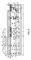
- FIG. 1 to FIG. 6show a series of schematic cross-sectional diagrams illustrating the results of progressive stages in fabricating a CMOS image sensor in accordance with an embodiment of the invention.
- FIG. 7 and FIG. 8show a pair of schematic plan-view diagrams illustrating an active pixel region and a dark pixel region generally in accordance with the embodiment of the invention that is illustrated within FIG. 1 to FIG. 6 .
- the instant inventionwhich includes an interconnect layout (i.e., wiring pattern) for use within an image sensor, the image sensor that includes the interconnect layout and a method for fabricating the image sensor, will be described in further detail within the context of the following description. The description is further understood within the context of the drawings described above.
- the drawingsare intended for illustrative purposes and as such the drawings are not necessarily drawn to scale.
- FIG. 1 to FIG. 6show a series of schematic cross-sectional diagrams illustrating the results of progressive stages in fabricating a CMOS image sensor in accordance with an embodiment of the invention.
- FIG. 1in particular shows a schematic cross-sectional diagram of the CMOS image sensor at an early stage in the fabrication thereof in accordance with the embodiment.
- FIG. 1shows a semiconductor substrate 10 .
- a counter-doped well 11(having a conductivity type different from the semiconductor substrate 10 ) is located within the semiconductor substrate 10 .
- a series of isolation regions 12is also located within the semiconductor substrate 10 .
- the semiconductor substrate 10comprises a first region R 1 that comprises an active pixel region, a laterally adjacent second region R 2 that comprises a dark pixel region and a further laterally adjacent third region R 3 that comprises a circuitry region.
- the semiconductor substrate 10may comprise any of several semiconductor materials.
- semiconductor materialsinclude silicon, germanium, silicon-germanium alloy, silicon carbide, silicon-germanium carbide alloy and compound semiconductor materials.
- Non-limiting examples of compound semiconductor materialsinclude gallium arsenide, indium arsenide and indium phosphide semiconductor materials.
- the semiconductor substrate 10comprises a silicon or silicon-germanium alloy semiconductor material that has a thickness from about 1 to about 3 mils.
- the series of isolation regions 12separates a series of photosensor regions 14 .
- the series of isolation regions 12separates a plurality of active regions.
- the active regions within the circuitry regioninclude a first field effect transistor T 1 and a second field effect transistor T 2 located and fabricated therein.
- the field effect transistors T 1 and T 2comprises a pair of CMOS transistors, since transistor T 1 is located and fabricated within the semiconductor substrate 10 and transistor T 2 is located and fabricated within the doped well 11 (having different conductivity type than the semiconductor substrate 10 ).
- the series of isolation regions 12may comprise materials, have dimensions and be formed using methods that are otherwise generally conventional in the semiconductor fabrication art.
- the isolation regions 12may include, but are not limited to, local oxidation of silicon (LOCOS) isolation regions, shallow trench isolation regions (i.e., having a depth up to about 5000 angstroms) and deep trench isolation regions (i.e., having a depth up to about 60000 angstroms).
- LOClocal oxidation of silicon
- shallow trench isolation regionsi.e., having a depth up to about 5000 angstroms
- deep trench isolation regionsi.e., having a depth up to about 60000 angstroms.
- the embodimentuses shallow trench isolation regions that are located within shallow isolation trenches.
- the isolation regions 12may comprise any of several dielectric materials. Typically included are oxides, nitrides and oxynitrides of silicon, as well as laminates thereof and composites thererof. Oxides, nitrides and oxynitrides of other elements are not excluded.
- the dielectric materials which may comprise the isolation regions 12are formed at least in part using a blanket layer deposition and planarizing method.
- Appropriate blanket layersmay be formed using methods including but not limited to thermal or plasma oxidation or nitridation methods, chemical vapor deposition methods and physical vapor deposition methods.
- Planarization methodsmay include, but are not limited to mechanical planarizing methods and chemical mechanical polish (CMP) planarizing methods. Chemical mechanical polish planarizing methods are most common.
- the isolation regions 12comprise at least in part a silicon oxide material that has a thickness from about 1000 to about 5000 angstroms.
- each of the photosensor regions 14may comprise photosensors that are otherwise generally conventional in the semiconductor fabrication art.
- Each of the photosensor regions 14typically comprises a photodiode, although the invention is not limited to a photosensor region 14 using only a photodiode.
- charge coupled devicesare also known to be used within photosensors.
- the photodiodeif used is doped to a concentration from about 1e16 to about 1e18 dopant atoms per cubic centimeter, while using an appropriate dopant.
- the photosensor region 14 plan-view linewidthsare typically from about 6.0 to about 1.5 microns.
- each of the field effect transistors T 1 and T 2comprises a gate dielectric 16 located upon the semiconductor substrate 10 .
- a gate 18is located aligned upon the gate dielectric 16 , although such alignment is not necessarily a feature of the invention.
- a plurality of spacers 20(illustrated as plural layers in cross-section but intended as single layers that surround the individual gates 18 in plan-view) is located adjoining the sidewalls of the gate dielectrics 16 and the gates 18 .
- each of the first transistor T 1 and the second transistor T 2comprises a pair of source/drain regions 22 separated by a channel region located beneath a corresponding gate 18 .
- Each of the foregoing layers and structures that comprise the first transistor T 1 and the second transistor T 2may comprise materials and have dimensions that are conventional in the semiconductor fabrication art. Each of the foregoing layers and structures that comprise the first transistor T 1 and the second transistor T 2 may also be formed using methods that are conventional in the semiconductor fabrication art.
- the gate dielectrics 16may comprise any of several gate dielectric materials. Included but not limiting are generally lower dielectric constant gate dielectric materials such as but not limited to oxides, nitrides and oxynitrides of silicon having a dielectric constant from about 4 to about 20, measured in vacuum. Also included, and also not limiting, are generally higher dielectric constant gate dielectric materials having a dielectric constant from about 20 to at least about 100. These higher dielectric constant gate dielectric materials may include, but are not limited to hafnium oxides, hafnium silicates, titanium oxides, lanthanum oxides, barium-strontium titanates (BSTs) and lead-zirconate titanates (PZTs).
- BSTsbarium-strontium titanates
- PZTslead-zirconate titanates
- the foregoing gate dielectric materialsmay be formed using methods appropriate to their materials of composition.
- Non-limiting examples of methodsinclude thermal or plasma oxidation or nitridation methods, chemical vapor deposition methods (including atomic layer chemical vapor deposition methods) and physical vapor deposition methods (including sputtering methods).
- the gate dielectrics 16comprise a thermal silicon oxide gate dielectric material having a thickness from about 20 to about 70 angstroms.
- the gates 18may similarly also comprise any of several gate conductor materials.
- Non-limiting examplesinclude certain metals, metal alloys, metal silicides and metal nitrides, as well as doped polysilicon materials (i.e., having a dopant concentration from about 1e18 to about 1e22 dopant atoms per cubic centimeter) and polycide (i.e., doped polysilicon/metal silicide stack) materials.
- the gate conductor materialsmay be formed using any of several methods. Non-limiting examples include chemical vapor deposition methods (also including atomic layer chemical vapor deposition methods) and physical vapor deposition methods (including sputtering methods).
- each of the gates 18comprises a doped polysilicon material having a thickness from about 1000 to about 1500 angstroms.
- the spacers 20typically comprise a dielectric spacer material or a laminate of dielectric spacer materials, although spacer layers comprising conductor materials are also known. Oxides, nitrides and oxynitrides of silicon are commonly used as dielectric spacer materials. Oxides, nitrides and oxynitrides of other elements are not excluded.
- the dielectric spacer materialsmay be deposited using methods analogous, equivalent or identical to the methods used for forming the gate dielectrics 16 .
- the spacers 20are formed using a blanket layer deposition and etchback method that provides the spacers 20 with the characteristic inward pointed shape.
- the source/drain regions 22are typically formed using a two-step ion implantation method.
- the source/drain regions 22are implanted with a dopant of polarity appropriate to a polarity of a field effect transistor within which they are formed.
- the two-step ion implantation methoduses a gate 18 , with and without a spacer 20 , as a mask.
- Typical concentrations of dopants within the source/drain regions 22are from about 1e15 to about 1e22 dopant atoms per cubic centimeter.
- FIG. 1Reference numerals for the gate dielectrics 16 , the gates 18 , the spacers 20 and the source/drain regions 22 for the first transistor T 1 and the second transistor T 2 are illustrated specifically in FIG. 1 . However, for clarity the reference numerals 16 / 18 / 20 / 22 are largely omitted within subsequent cross-sectional diagrams, although the first transistor and the second transistor are still designated as T 1 and T 2 .
- FIG. 2shows the results of further processing of the CMOS image sensor whose schematic cross-sectional diagram is illustrated in FIG. 1 .
- FIG. 2shows a dielectric/contact stud layer 23 located upon the CMOS image sensor whose schematic cross-sectional diagram is illustrated in FIG. 1 .
- the dielectric/contact stud layer 23comprises a dielectric layer 24 and a plurality of contact studs 25 .
- the dielectric layer 24may comprise any of several dielectric materials. Included but not limiting are oxides, nitrides and oxynitrides of silicon. Oxides, nitrides and oxynitrides of other elements are not excluded. Also included are crystalline as well as amorphous dielectric materials.
- comparatively dense dielectric materialssuch as silicon oxides, silicon nitrides and silicon oxynitrides deposited using chemical vapor deposition methods and physical vapor deposition methods (i.e., having a generally higher dielectric constant in a range from about 4 to about 20); as well as (2) comparatively less dense or porous dielectric materials such as spin-on-glass and spin-on-polymer dielectric materials (having a generally lower dielectric constant in a range from about 2.5 to about 4).
- the dielectric materialsmay be formed using any of several methods. Included are thermal or plasma oxidation or nitridation methods, chemical vapor deposition methods, physical vapor deposition methods and spin-on methods.
- the dielectric layer 24comprises at least in part a silicon oxide material having a thickness from about 3000 to about 9000 angstroms.
- the contact studs 25may comprise any of several conductor materials. Included but not limiting are certain metals, metal alloys, doped polysilicon and polycide conductor materials. Metals such as tungsten, aluminum and copper are generally common conductor materials.
- the conductor stud materialsmay be deposited using methods that are appropriate to their materials of composition. Included are plating methods, chemical vapor deposition methods and physical vapor deposition methods.
- the contact studs 25comprise a tungsten conductor material for purposes of effecting optimal electrical contact and conduction to the first transistor T 1 and the second transistor T 2 .
- a blanket precursor layer to the dielectric layer 24is first formed upon the semiconductor structure of FIG. 1 .
- This precursor dielectric layeris then patterned to expose a source/drain region 22 within each of the first transistor T 1 and the second transistor T 2 .
- a blanket tungsten layer(or alternatively another conductor material layer) is deposited and located upon the resulting patterned dielectric layer 24 and planarized to form the contact studs 25 .
- the planarizationmay be effected using methods including but not limited to purely mechanical planarizing methods, as well as chemical mechanical polish planarizing methods. Chemical mechanical polish planarizing methods are generally more common, but they do not limit the invention.
- FIG. 3shows a dielectric/interconnect layer 27 located upon the semiconductor structure whose schematic cross-sectional diagram is illustrated in FIG. 2 .
- the dielectric/interconnect layer 27comprises a dielectric layer 28 and a plurality of interconnect layers 29 and 29 ′.
- the plurality of interconnect layers 29 and 29 ′has a different spatial pattern P 1 (i.e., a less dense spatial pattern) within the region R 1 that comprises the active pixels than a spatial pattern P 2 (i.e., a more dense spatial pattern) within the region R 2 that comprises the dark pixel.
- the spatial pattern P 1does not include any interconnect layers 29 or 29 ′ within a light path with respect to a photosensor region 14 within the region R 1 comprising the active pixels.
- the spatial pattern P 2does include an interconnect layer 29 ′ that is nominally centered above the photosensor region 14 within the region R 2 comprising the dark pixel. Interconnect layer 29 ′ is thus clearly within a light path with respect to the photosensor region 14 within the region R 2 comprising the dark pixel, and interconnect layer 29 ′ would be within a light path with respect to one of the photosensor regions 14 within the region R 1 comprising the active pixels if included within the pattern P 1 .
- the dielectric layer 28may comprise dielectric materials and be formed using methods similar to the materials and methods that are used within the context of the dielectric layer 24 .
- the interconnect layers 29 and 29 ′may comprise any of the several conductor materials from which may be comprised the contact studs 25 .
- the interconnect layers 29 and 29 ′comprise copper conductor materials, although the invention is not so limited.
- the dielectric/interconnect layer 27has a thickness from about 1000 to about 5000 angstroms.
- the dielectric/interconnect layer 27may be formed using methods that are generally analogous to the methods used for forming the dielectric/contact stud layer 23 .
- a precursor layer to the dielectric layer 28is formed and patterned to form the dielectric layer 28 .
- a blanket interconnect conductor layeris then formed and located upon the dielectric layer 28 and planarized to form the interconnect layers 29 and 29 ′.
- FIG. 4shows a dielectric/stud-interconnect layer 31 located upon the dielectric/interconnect layer 27 illustrated within the schematic cross-sectional diagram of FIG. 3 .
- the dielectric/stud-interconnect layer 31comprises dielectric layer 32 and stud-interconnect layers 33 and 33 ′, some of which are not of appropriate cross-section to illustrate stud portions of stud-interconnect layers 33 and 33 ′.
- the dielectric layer 32may comprise materials and be formed using methods generally analogous to the materials and methods used for forming the dielectric layers 28 and 24 .
- the stud-interconnect layers 33 and 33 ′may comprise materials and be formed using methods generally analogous to the materials and methods used for forming the interconnect layers 29 and 29 ′ or the stud layers 25 .
- the methods for forming the stud-interconnect layers 33 and 33 ′will comprise dual damascene methods rather than the single damascene methods disclosed above within the context of forming the interconnect layers 29 and 29 ′′ within the dielectric/interconnect layer 27 and the stud layers 25 within the dielectric/stud layer 23 .
- Such a dual damascene methodfirst provides for forming a contiguous trench and via within a precursor layer to the dielectric layer 32 . Either the trench or the via may be formed first.
- a blanket stud-interconnect material layeri.e., typically copper, but the invention is not so limited
- the blanket stud-interconnect material layeris then planarized to form the stud-interconnect layers 33 and 33 ′.
- the dielectric/stud-interconnect layer 31has a thickness from about 3000 to about 9000 angstroms.
- the stud-interconnect layers 33 and 33 ′also have a different spatial pattern P 1 ′ in the first region R 1 comprising the active pixels, in comparison with a spatial pattern P 2 ′ in the second region R 2 comprising the dark pixel.
- none of the stud-interconnect layers 33 or 33 ′is within a light path with respect to the photosensor regions 14 within the first region R 1 comprising the active pixels.
- stud-interconnect layers 33 ′are located within a light path with respect to the photosensor region 14 within the second region R 2 comprising the dark pixel.
- the embodimentprovides interconnect wiring layers (i.e., interconnect layer 29 ′ and stud-interconnect layers 33 ′) that are located within a light path with respect to the photosensor region 14 within the region R 2 comprising the dark pixel.
- interconnect wiring layersi.e., interconnect layer 29 ′ and stud-interconnect layers 33 ′
- similar wiring layersi.e., interconnect layers 29 and stud-interconnect layers 33
- FIG. 5shows a schematic cross-sectional diagram illustrating the results of further processing of the semiconductor structure of FIG. 4 .
- FIG. 5first shows dielectric/terminal stud layer 35 located upon the dielectric/stud-interconnect layer 31 .
- the dielectric/terminal stud layer 35comprises a dielectric layer 36 and a terminal stud layer 37 .
- the dielectric layer 36may comprise materials and be formed using methods that are analogous, equivalent or identical to the materials and methods used for forming the dielectric layers 32 , 28 and 24 .
- the stud layer 37may comprise materials and be formed using methods, analogous, equivalent or identical to the materials and methods used for forming the stud layers 25 .
- the dielectric/terminal stud layer 35has a thickness from about 2000 to about 6000 angstroms.
- FIG. 5also shows a plurality of interconnect layers 38 , a light shield layer 38 ′′ and a bond pad 38 ′′ located upon the dielectric/terminal stud layer 35 .
- the bond pad 38 ′′contacts the terminal stud 37 .
- the interconnect layers 38 , the light shield layer 38 ′ and the bond pad 38 ′′are typically patterned from a single blanket metal layer. Metals from which may be comprised the blanket metal layer include but are not limited to aluminum, copper and tungsten. Aluminum is more common, since aluminum is often desirable as a bond pad material. The invention is not so limited.
- each of the interconnect layers 38 , the light shield layer 38 ′ and the bond pad 38 ′′has a thickness from about 2000 to about 9000 angstroms.
- FIG. 5shows a schematic cross-sectional diagram of a CMOS image sensor having an electrically active first physical interconnect pattern P 1 ′′ within the region R 1 comprising the active pixels that is spatially different from an electrically active second physical interconnect pattern P 2 ′′ within the region R 2 comprising the dark pixel.
- the electrically active second physical interconnect pattern P 2 ′′includes the interconnect layer 29 ′ and the stud-interconnect layers 33 ′ interposed between the light shield 38 ′ and the photosensor region 14 within the region R 2 comprising the dark pixel.
- the interconnect layer 29 ′ and the stud-interconnect layers 33 ′would thus be within a light path within the region R 2 comprising the dark pixel, but for the presence of the light shield 38 ′.
- the interconnect layer 29 ′ and the stud-interconnect layers 33 ′are not included within the electrically active first physical interconnect pattern P 1 ′′ within the first region R 1 comprising the active pixels, but would be within a light path with respect to a photosensor region 14 if included within the electrically active first physical interconnect pattern P 1 ′′.
- the CMOS image sensorBy locating the interconnect layer 29 ′ and the stud-interconnect layers 33 ′ within the space available interposed between the light shield 38 ′ and the photosensor region 14 within the region R 2 comprising the dark pixel, the CMOS image sensor whose schematic cross-sectional diagram is illustrated in FIG. 5 provides for enhanced flexibility in the design and implementation of interconnect circuitry.
- the use of the space available interposed between the light shield 38 ′ and the photosensor 14 within the region R 2 comprising the dark pixel for additional interconnect circuitryalso potentially allows for use of a lesser number of metallization levels (i.e., a number of vertical metallization layers) when fabricating a CMOS image sensor.
- FIG. 6shows the results of further processing of the CMOS image sensor whose schematic cross-sectional diagram is illustrated in FIG. 5 .
- FIG. 6first shows a passivation layer 39 located conformally upon the semiconductor structure of FIG. 5 .
- the passivation layer 39passivates the interconnect layers 38 , the light shield 38 ′ and the bond pad 38 ′′.
- Located upon the passivation layer 39is a planarizing layer 40 .
- the passivation layer 39typically comprises a bilayer of materials, as is illustrated within FIG. 6 .
- the bilayertypically comprises a lower layer 39 a predominantly comprising an oxide material and an upper layer 39 b predominantly comprising a nitride material.
- the oxide material and the nitride materialmay be formed using methods analogous to the methods used for forming underlying dielectric layers 36 / 32 / 28 / 24 within the CMOS image sensor that is illustrated in FIG. 6 .
- the lower layer 39 ahas a thickness from about 500 to about 5000 angstroms and the upper layer 39 b has a thickness from about 500 to about 5000 angstroms.
- the planarizing layer 40may comprise any of several optically transparent planarizing materials. Non-limiting examples include spin-on-glass planarizing materials and spin-on-polymer planarizing materials that may include, but are not limited to spin-on-polymers such as but not limited to photoresist materials.
- the planarizing layer 40has a thickness sufficient to at least planarize the interconnect layers 38 , the light shield 38 ′ and the bond pad 38 ′′, thus providing a planar surface for fabrication of additional structures within the CMOS image sensor whose schematic cross-sectional diagram is illustrated in FIG. 6 .
- the planarizing layer 40has a thickness from about 2000 to about 9000 angstroms within the context of the foregoing planarization limitations.
- FIG. 6also shows a plurality of color filter layers 42 a , 42 b and 42 c located upon tle planarizing layer 40 .
- Each of the plurality of color filter layers 42 a , 42 b and 42 cis aligned and registered with respect to one of the photosensor regions 14 .
- the color filter layers 42 a , 42 b and 42 cwill typically include either the primary colors of red, green and blue, or the complementary colors of yellow, cyan and magenta.
- the color filter layers 42 a , 42 b and 42 ctypically comprise a series of dyed or pigmented patterned photoresist layers that is intrinsically imaged to form the series of color filter layers 42 a , 42 b and 42 c .
- the color filter layers 42 a , 42 b and 42 cmay comprise dyed or pigmented organic polymer materials that are otherwise optically transparent, but extrinsically imaged while using an appropriate mask layer. Alternative color filter materials may also be used.
- FIG. 6finally shows a plurality of lens layers 44 located upon the color filter layers 42 a , 42 b and 42 c .
- the lens layers 44may comprise any of several optically transparent lens materials that are known in the art. Non-limiting examples include optically transparent inorganic materials, optically transparent organic materials and optically transparent composite materials. Most common are optically transparent organic materials.
- the lens layers 44are formed incident to patterning and reflow of an organic polymer material that has a glass transition temperature lower than the series of color filter layers 42 a , 42 b and 42 c or the planarizing layer 40 . Other methods and materials may alternatively be used.
- FIG. 6shows a schematic cross-sectional diagram of a CMOS image sensor in accordance with an embodiment of the invention.
- the CMOS image sensorcomprises the first region R 1 comprising the plurality active pixels and the second region R 2 comprising the dark pixel that includes the light shield 38 ′′.
- the CMOS image sensoralso comprises the third region R 3 that comprises circuitry including the first transistor T 1 and the second transistor T 2 .
- the CMOS image sensoralso comprises a multi-layer interconnect layer comprising the dielectric/contact stud layer 23 , the dielectric/interconnect layer 27 , the dielectric/stud-interconnect layer 31 , the dielectric/terminal stud layer 35 and the interconnect layers 38 .
- the multi-level interconnect layercomprises a first electrically active interconnect pattern P 1 ′′′ within the first region R 1 that comprises the active pixels and a second electrically active interconnect pattern P 2 ′′′ spatially different from the first electrically active interconnect pattern P 1 ′′′ within the second region R 2 that comprises the dark pixel.
- the second electrically active interconnect pattern P 2 ′′′ within the region R 2 that comprises the dark pixelincludes electrically active interconnect layer 29 ′ and stud-interconnect layers 33 ′ interposed between the light shield 38 ′ and the photosensor region 14 .
- the electrically active interconnect layer 29 ′ and stud-interconnect layers 33 ′would otherwise be within a light path between the lens layer 44 and the photosensor region 14 within the second region R 2 if the light shield 38 ′ was absent.
- the use of these additional electrically active interconnect layer 29 ′ and stud-interconnect layers 33 ′ interposed between the light shield 38 ′ and the photosensor region 14 within the second region R 2allows for design of additional circuitry within the CMOS image sensor at a location which is otherwise unused. Design and implementation of this additional circuitry also allows for the CMOS image sensor to be fabricated with a lesser number of metal levels. By using a lesser number of metal levels, a CMOS image sensor may be fabricated more efficiently and with less expenditure of manufacturing resource.
- CMOS image sensorcomprising three interconnect metal levels (i.e., interconnect layers 29 and 29 ′, stud-interconnect layers 33 and 33 ′ and interconnect layers 38 )
- the inventionis clearly not limited to the foregoing embodiment. Rather an additional embodiment may comprise additional interconnect layers beyond the interconnect layers illustrated within the CMOS image sensor whose schematic cross-sectional diagram is illustrated in FIG. 6 .
- FIG. 7 and FIG. 8show schematic plan-view diagrams illustrating an active pixel region generally, but not specifically, in accordance with the CMOS image sensor of FIG. 5 and a dark pixel region generally, but not specifically, in accordance with the CMOS image sensor of FIG. 4 .
- FIG. 7shows a plurality of photosensor regions 14 illustrated in the foregoing cross-sectional diagrams and a plurality of transfer gates 15 that are not illustrated within the foregoing cross-sectional diagrams.
- FIG. 7also shows a plurality of first interconnect layers 29 , second interconnect layers 33 and third interconnect layers 38 .
- FIG. 7also shows dense interconnect regions 45 .
- the plurality of photosensor regions 14is largely exposed to an incoming light path.
- FIG. 8also shows the plurality of photosensor regions 14 , transfer gates 15 , first interconnect layers 29 / 29 ′ and second interconnect layers 33 / 33 ′.
- Third interconnect layers that include light shieldsare omitted within FIG. 8 . As is illustrated within the schematic plan-view diagram of FIG.
- first interconnect layers 29 / 29 ′i.e., the portions designated as first interconnect layers 29 ′
- second interconnect layers 33 / 33 ′i.e., the portions designated as second interconnect layers 33 ′
- the plan-view diagrams of FIG. 7 and FIG. 8also illustrate a CMOS image sensor in accordance with an embodiment of the invention.
- the CMOS image sensorincludes electrically active interconnect layers 29 ′ and 33 ′ interposed between the light shield layers (not shown) and the photosensor regions 14 within dark pixel regions but not active pixel regions.
- These additional electrically active interconnect layers 29 ′ and 33 ′ that are within a light path with respect to photosensor regions 14 within the dark pixel regionallow for greater functionality and fewer metal levels when fabricating a CMOS image sensor array. Thus use of fewer metal levels provides for enhanced manufacturing efficiency.
Landscapes
- Solid State Image Pick-Up Elements (AREA)
Abstract
Description
- This application is a divisional of U.S. application Ser. No. 11/560,019, filed Nov. 15, 2006.
- 1. Field of the Invention
- The invention relates generally to pixels within image sensors. More particularly, the invention relates to interconnect patterns within pixels within image sensors.
- 2. Description of Related Art
- Semiconductor image sensors, including complementary metal oxide semiconductor (CMOS) image sensors and charge coupled device (CCD) image sensors, are gaining in popularity. In general, semiconductor image sensors are used as imaging components within various types of consumer and industrial products. Non-limiting examples of applications for image sensors include scanners, photocopiers, digital cameras and video telecommunications devices. CMOS image sensors provide advantages in comparison with other types of semiconductor image sensors insofar as CMOS image sensors are generally less expensive to fabricate. CMOS image sensors also generally consume less power.
- Image sensors typically comprise an array of pixels that in turn comprises an array of photosensors located within a semiconductor substrate. The photosensors are often photodiodes. Aligned over the array of photosensors is an array of lens structures (or lens layers) that is used to capture incoming light that is representative of an object desired to be imaged. Interposed between the array of photosensors and the array of lens structures are spacer layers and color filter layers that allow for color discrimination and focusing of incoming light.
- Image sensors also typically include dark pixels (i.e., pixels from which light is excluded) in addition to active pixels (i.e., pixels that are actively used within an imaging application). An electrical output from a dark pixel is typically used to determine a background response of a pixel, for purposes of electrical correction for active pixel output within the image sensor.
- Pixel dimensions within image sensors are certain to continue to decrease and such decreased pixel dimensions within image sensors are likely to lead to a need for more efficient image sensor structures and methods for fabrication thereof. Included are sensors that include dark pixel correction. Thus, desirable are image sensors, and methods for fabrication thereof, that efficiently provide for dark pixel correction.
- The invention includes an interconnect wiring pattern for a sensor array, the sensor array that includes the interconnect wiring pattern and a method for fabricating the sensor array. Within the interconnect pattern, sensor array and method for fabrication thereof, a first electrically active interconnect wiring pattern is used within an active pixel region and a second electrically active interconnect wiring pattern spatially different from the first electrically active interconnect wiring pattern is used within a dark pixel region.
- The second electrically active interconnect wiring pattern includes at least one interconnect layer that if included within the first electrically active interconnect pattern would be within a light path.
- Within the embodiment and the invention, an “electrically active” interconnect wiring pattern is intended to exclude portions of wiring patterns that are used in light shield layers within dark pixel regions. “Electrically active” interconnect wiring patterns are thus in general also intended to primarily include portions of wiring patterns that are actively used in electrical signal sensing or propagation.
- Within the embodiment and the invention, “spatially different” with respect to a comparison of a first electrically active wiring pattern used within an active pixel region and a second electrically active wiring pattern used within a dark pixel region is intended to indicate a different geometric arrangement of wiring layers within the first electrically active wiring pattern and the second electrically active wiring pattern. The different geometric arrangement may include, but is not limited to a density of wiring layers, a separation distance of wiring layers and a specific spatial location of wiring layers.
- An interconnect layout (i.e., wiring pattern) for a sensor array in accordance with the invention includes a first electrically active physical interconnect pattern located within a plurality of active pixels. The interconnect layout also includes a second electrically active physical interconnect pattern spatially different from the first electrically active physical interconnect pattern located within a plurality of dark pixels. The second electrically active physical interconnect pattern includes at least one interconnect layer not included within the first electrically active physical interconnect pattern that would be spatially located in a light path if included within the first electrically active physical interconnect pattern.
- An image sensor in accordance with the invention includes a plurality of photosensor regions located within a substrate. The image sensor also includes a multi-layer interconnect layer located over the substrate including the plurality of photosensor regions. The multi-layer interconnect layer comprises a first electrically active pattern within a plurality of active pixel regions and a second electrically active pattern spatially different from the first electrically active pattern within a plurality of dark pixel regions. Within the image sensor, the second electrically active pattern comprises at least one interconnect layer not included within the first electrically active pattern that would be spatially located in a light path if included within the first electrically active pattern
- A method for fabricating an image sensor in accordance with the invention includes forming a multi-layer interconnect layer over a substrate comprising a plurality of photosensor regions. The method provides that the plurality of photosensor regions comprises a plurality of dark pixels and a plurality of active pixels. The method also provides that the multi-layer interconnect layer has a first electrically active pattern with respect to the plurality of active pixels and a second electrically active pattern spatially different from the first electrically active pattern with respect to the plurality of dark pixels. Within the method, the second electrically active pattern comprises at least one interconnect layer not included within the first electrically active pattern that would be spatially located in a light path if formed within the first electrically active pattern
- The objects, features and advantages of the invention are understood within the context of the Description of the Preferred Embodiments, as set forth below. The Description of the Preferred Embodiments is understood within the context of the accompanying drawings, which form a material part of this disclosure, wherein:
FIG. 1 toFIG. 6 show a series of schematic cross-sectional diagrams illustrating the results of progressive stages in fabricating a CMOS image sensor in accordance with an embodiment of the invention.FIG. 7 andFIG. 8 show a pair of schematic plan-view diagrams illustrating an active pixel region and a dark pixel region generally in accordance with the embodiment of the invention that is illustrated withinFIG. 1 toFIG. 6 .- The instant invention, which includes an interconnect layout (i.e., wiring pattern) for use within an image sensor, the image sensor that includes the interconnect layout and a method for fabricating the image sensor, will be described in further detail within the context of the following description. The description is further understood within the context of the drawings described above. The drawings are intended for illustrative purposes and as such the drawings are not necessarily drawn to scale.
FIG. 1 toFIG. 6 show a series of schematic cross-sectional diagrams illustrating the results of progressive stages in fabricating a CMOS image sensor in accordance with an embodiment of the invention.FIG. 1 in particular shows a schematic cross-sectional diagram of the CMOS image sensor at an early stage in the fabrication thereof in accordance with the embodiment.FIG. 1 shows asemiconductor substrate 10. A counter-doped well11 (having a conductivity type different from the semiconductor substrate10) is located within thesemiconductor substrate 10. A series ofisolation regions 12 is also located within thesemiconductor substrate 10. Thesemiconductor substrate 10 comprises a first region R1 that comprises an active pixel region, a laterally adjacent second region R2 that comprises a dark pixel region and a further laterally adjacent third region R3 that comprises a circuitry region.- The
semiconductor substrate 10 may comprise any of several semiconductor materials. Non-limiting examples of semiconductor materials include silicon, germanium, silicon-germanium alloy, silicon carbide, silicon-germanium carbide alloy and compound semiconductor materials. Non-limiting examples of compound semiconductor materials include gallium arsenide, indium arsenide and indium phosphide semiconductor materials. Typically, thesemiconductor substrate 10 comprises a silicon or silicon-germanium alloy semiconductor material that has a thickness from about 1 to about 3 mils. - Within the first region R1 and the second region R2, the series of
isolation regions 12 separates a series ofphotosensor regions 14. Within the third region R3, the series ofisolation regions 12 separates a plurality of active regions. The active regions within the circuitry region include a first field effect transistor T1 and a second field effect transistor T2 located and fabricated therein. The field effect transistors T1 and T2 comprises a pair of CMOS transistors, since transistor T1 is located and fabricated within thesemiconductor substrate 10 and transistor T2 is located and fabricated within the doped well11 (having different conductivity type than the semiconductor substrate10). - Within the first region R1, the second region R1 and the third region R3, the series of
isolation regions 12 may comprise materials, have dimensions and be formed using methods that are otherwise generally conventional in the semiconductor fabrication art. - The
isolation regions 12 may include, but are not limited to, local oxidation of silicon (LOCOS) isolation regions, shallow trench isolation regions (i.e., having a depth up to about 5000 angstroms) and deep trench isolation regions (i.e., having a depth up to about 60000 angstroms). Typically, the embodiment uses shallow trench isolation regions that are located within shallow isolation trenches. The isolation regions12 (whether located within shallow isolation trenches or deep isolation trenches) may comprise any of several dielectric materials. Typically included are oxides, nitrides and oxynitrides of silicon, as well as laminates thereof and composites thererof. Oxides, nitrides and oxynitrides of other elements are not excluded. - Typically, the dielectric materials which may comprise the
isolation regions 12 are formed at least in part using a blanket layer deposition and planarizing method. Appropriate blanket layers may be formed using methods including but not limited to thermal or plasma oxidation or nitridation methods, chemical vapor deposition methods and physical vapor deposition methods. Planarization methods may include, but are not limited to mechanical planarizing methods and chemical mechanical polish (CMP) planarizing methods. Chemical mechanical polish planarizing methods are most common. Typically theisolation regions 12 comprise at least in part a silicon oxide material that has a thickness from about 1000 to about 5000 angstroms. - Within the first region R1 and the second region R1, each of the
photosensor regions 14 may comprise photosensors that are otherwise generally conventional in the semiconductor fabrication art. Each of thephotosensor regions 14 typically comprises a photodiode, although the invention is not limited to aphotosensor region 14 using only a photodiode. As noted above, charge coupled devices are also known to be used within photosensors. Typically, the photodiode (if used) is doped to a concentration from about 1e16 to about 1e18 dopant atoms per cubic centimeter, while using an appropriate dopant. Thephotosensor region 14 plan-view linewidths (in both directions) are typically from about 6.0 to about 1.5 microns. - Within the third region R3, each of the field effect transistors T1 and T2 comprises a
gate dielectric 16 located upon thesemiconductor substrate 10. Agate 18 is located aligned upon thegate dielectric 16, although such alignment is not necessarily a feature of the invention. A plurality of spacers20 (illustrated as plural layers in cross-section but intended as single layers that surround theindividual gates 18 in plan-view) is located adjoining the sidewalls of thegate dielectrics 16 and thegates 18. Finally, each of the first transistor T1 and the second transistor T2 comprises a pair of source/drain regions 22 separated by a channel region located beneath a correspondinggate 18. - Each of the foregoing layers and structures that comprise the first transistor T1 and the second transistor T2 may comprise materials and have dimensions that are conventional in the semiconductor fabrication art. Each of the foregoing layers and structures that comprise the first transistor T1 and the second transistor T2 may also be formed using methods that are conventional in the semiconductor fabrication art.
- The gate dielectrics16 may comprise any of several gate dielectric materials. Included but not limiting are generally lower dielectric constant gate dielectric materials such as but not limited to oxides, nitrides and oxynitrides of silicon having a dielectric constant from about 4 to about 20, measured in vacuum. Also included, and also not limiting, are generally higher dielectric constant gate dielectric materials having a dielectric constant from about 20 to at least about 100. These higher dielectric constant gate dielectric materials may include, but are not limited to hafnium oxides, hafnium silicates, titanium oxides, lanthanum oxides, barium-strontium titanates (BSTs) and lead-zirconate titanates (PZTs).
- The foregoing gate dielectric materials may be formed using methods appropriate to their materials of composition. Non-limiting examples of methods include thermal or plasma oxidation or nitridation methods, chemical vapor deposition methods (including atomic layer chemical vapor deposition methods) and physical vapor deposition methods (including sputtering methods). Typically, the
gate dielectrics 16 comprise a thermal silicon oxide gate dielectric material having a thickness from about 20 to about 70 angstroms. - The
gates 18 may similarly also comprise any of several gate conductor materials. Non-limiting examples include certain metals, metal alloys, metal silicides and metal nitrides, as well as doped polysilicon materials (i.e., having a dopant concentration from about 1e18 to about 1e22 dopant atoms per cubic centimeter) and polycide (i.e., doped polysilicon/metal silicide stack) materials. The gate conductor materials may be formed using any of several methods. Non-limiting examples include chemical vapor deposition methods (also including atomic layer chemical vapor deposition methods) and physical vapor deposition methods (including sputtering methods). Typically, each of thegates 18 comprises a doped polysilicon material having a thickness from about 1000 to about 1500 angstroms. - The
spacers 20 typically comprise a dielectric spacer material or a laminate of dielectric spacer materials, although spacer layers comprising conductor materials are also known. Oxides, nitrides and oxynitrides of silicon are commonly used as dielectric spacer materials. Oxides, nitrides and oxynitrides of other elements are not excluded. The dielectric spacer materials may be deposited using methods analogous, equivalent or identical to the methods used for forming thegate dielectrics 16. Typically, thespacers 20 are formed using a blanket layer deposition and etchback method that provides thespacers 20 with the characteristic inward pointed shape. - The source/
drain regions 22 are typically formed using a two-step ion implantation method. The source/drain regions 22 are implanted with a dopant of polarity appropriate to a polarity of a field effect transistor within which they are formed. The two-step ion implantation method uses agate 18, with and without aspacer 20, as a mask. Typical concentrations of dopants within the source/drain regions 22 are from about 1e15 to about 1e22 dopant atoms per cubic centimeter. - Reference numerals for the gate dielectrics16, the
gates 18, thespacers 20 and the source/drain regions 22 for the first transistor T1 and the second transistor T2 are illustrated specifically inFIG. 1 . However, for clarity thereference numerals 16/18/20/22 are largely omitted within subsequent cross-sectional diagrams, although the first transistor and the second transistor are still designated as T1 and T2. FIG. 2 shows the results of further processing of the CMOS image sensor whose schematic cross-sectional diagram is illustrated inFIG. 1 .FIG. 2 shows a dielectric/contact stud layer 23 located upon the CMOS image sensor whose schematic cross-sectional diagram is illustrated inFIG. 1 . The dielectric/contact stud layer 23 comprises adielectric layer 24 and a plurality ofcontact studs 25.- The
dielectric layer 24 may comprise any of several dielectric materials. Included but not limiting are oxides, nitrides and oxynitrides of silicon. Oxides, nitrides and oxynitrides of other elements are not excluded. Also included are crystalline as well as amorphous dielectric materials. Further included are: (1) comparatively dense dielectric materials such as silicon oxides, silicon nitrides and silicon oxynitrides deposited using chemical vapor deposition methods and physical vapor deposition methods (i.e., having a generally higher dielectric constant in a range from about 4 to about 20); as well as (2) comparatively less dense or porous dielectric materials such as spin-on-glass and spin-on-polymer dielectric materials (having a generally lower dielectric constant in a range from about 2.5 to about 4). The dielectric materials may be formed using any of several methods. Included are thermal or plasma oxidation or nitridation methods, chemical vapor deposition methods, physical vapor deposition methods and spin-on methods. Typically, thedielectric layer 24 comprises at least in part a silicon oxide material having a thickness from about 3000 to about 9000 angstroms. - The
contact studs 25 may comprise any of several conductor materials. Included but not limiting are certain metals, metal alloys, doped polysilicon and polycide conductor materials. Metals such as tungsten, aluminum and copper are generally common conductor materials. The conductor stud materials may be deposited using methods that are appropriate to their materials of composition. Included are plating methods, chemical vapor deposition methods and physical vapor deposition methods. Typically, thecontact studs 25 comprise a tungsten conductor material for purposes of effecting optimal electrical contact and conduction to the first transistor T1 and the second transistor T2. - To fabricate the dielectric/
contact stud layer 23 that is illustrated inFIG. 2 upon the semiconductor structure whose schematic cross-sectional diagram is illustrated inFIG. 1 , a blanket precursor layer to thedielectric layer 24 is first formed upon the semiconductor structure ofFIG. 1 . This precursor dielectric layer is then patterned to expose a source/drain region 22 within each of the first transistor T1 and the second transistor T2. Finally, a blanket tungsten layer (or alternatively another conductor material layer) is deposited and located upon the resulting patterneddielectric layer 24 and planarized to form thecontact studs 25. The planarization may be effected using methods including but not limited to purely mechanical planarizing methods, as well as chemical mechanical polish planarizing methods. Chemical mechanical polish planarizing methods are generally more common, but they do not limit the invention. FIG. 3 shows a dielectric/interconnect layer 27 located upon the semiconductor structure whose schematic cross-sectional diagram is illustrated inFIG. 2 . The dielectric/interconnect layer 27 comprises adielectric layer 28 and a plurality of interconnect layers29 and29′. The plurality of interconnect layers29 and29′ has a different spatial pattern P1 (i.e., a less dense spatial pattern) within the region R1 that comprises the active pixels than a spatial pattern P2 (i.e., a more dense spatial pattern) within the region R2 that comprises the dark pixel. The spatial pattern P1 does not include anyinterconnect layers photosensor region 14 within the region R1 comprising the active pixels. The spatial pattern P2 does include aninterconnect layer 29′ that is nominally centered above thephotosensor region 14 within the region R2 comprising the dark pixel.Interconnect layer 29′ is thus clearly within a light path with respect to thephotosensor region 14 within the region R2 comprising the dark pixel, andinterconnect layer 29′ would be within a light path with respect to one of thephotosensor regions 14 within the region R1 comprising the active pixels if included within the pattern P1.- The
dielectric layer 28 may comprise dielectric materials and be formed using methods similar to the materials and methods that are used within the context of thedielectric layer 24. The interconnect layers29 and29′ may comprise any of the several conductor materials from which may be comprised thecontact studs 25. Typically the interconnect layers29 and29′ comprise copper conductor materials, although the invention is not so limited. Typically, the dielectric/interconnect layer 27 has a thickness from about 1000 to about 5000 angstroms. - The dielectric/
interconnect layer 27 may be formed using methods that are generally analogous to the methods used for forming the dielectric/contact stud layer 23. In particular, a precursor layer to thedielectric layer 28 is formed and patterned to form thedielectric layer 28. A blanket interconnect conductor layer is then formed and located upon thedielectric layer 28 and planarized to form the interconnect layers29 and29′. FIG. 4 shows a dielectric/stud-interconnect layer 31 located upon the dielectric/interconnect layer 27 illustrated within the schematic cross-sectional diagram ofFIG. 3 . The dielectric/stud-interconnect layer 31 comprisesdielectric layer 32 and stud-interconnect layers interconnect layers dielectric layer 32 may comprise materials and be formed using methods generally analogous to the materials and methods used for forming thedielectric layers interconnect layers - More particularly, the methods for forming the stud-
interconnect layers interconnect layer 27 and the stud layers25 within the dielectric/stud layer 23. - Such a dual damascene method first provides for forming a contiguous trench and via within a precursor layer to the
dielectric layer 32. Either the trench or the via may be formed first. A blanket stud-interconnect material layer (i.e., typically copper, but the invention is not so limited) is then formed to fill the via and the trench. The blanket stud-interconnect material layer is then planarized to form the stud-interconnect layers interconnect layer 31 has a thickness from about 3000 to about 9000 angstroms. - As is illustrated in
FIG. 4 , the stud-interconnect layers interconnect layers photosensor regions 14 within the first region R1 comprising the active pixels. However, stud-interconnect layers 33′ are located within a light path with respect to thephotosensor region 14 within the second region R2 comprising the dark pixel. - Thus, within the context of the schematic cross-sectional diagrams of
FIG. 3 andFIG. 4 , the embodiment provides interconnect wiring layers (i.e.,interconnect layer 29′ and stud-interconnect layers 33′) that are located within a light path with respect to thephotosensor region 14 within the region R2 comprising the dark pixel. The embodiment also provides that similar wiring layers (i.e., interconnect layers29 and stud-interconnect layers33) are not located within a light path with respect to thephotosensor regions 14 within the first region R1 comprising the active pixels. FIG. 5 shows a schematic cross-sectional diagram illustrating the results of further processing of the semiconductor structure ofFIG. 4 .FIG. 5 first shows dielectric/terminal stud layer 35 located upon the dielectric/stud-interconnect layer 31. The dielectric/terminal stud layer 35 comprises adielectric layer 36 and aterminal stud layer 37.- The
dielectric layer 36 may comprise materials and be formed using methods that are analogous, equivalent or identical to the materials and methods used for forming thedielectric layers stud layer 37 may comprise materials and be formed using methods, analogous, equivalent or identical to the materials and methods used for forming the stud layers25. Typically, the dielectric/terminal stud layer 35 has a thickness from about 2000 to about 6000 angstroms. FIG. 5 also shows a plurality of interconnect layers38, alight shield layer 38″ and abond pad 38″ located upon the dielectric/terminal stud layer 35. In particular, thebond pad 38″ contacts theterminal stud 37. The interconnect layers38, thelight shield layer 38′ and thebond pad 38″ are typically patterned from a single blanket metal layer. Metals from which may be comprised the blanket metal layer include but are not limited to aluminum, copper and tungsten. Aluminum is more common, since aluminum is often desirable as a bond pad material. The invention is not so limited. Typically, each of the interconnect layers38, thelight shield layer 38′ and thebond pad 38″ has a thickness from about 2000 to about 9000 angstroms.- Within the schematic cross-sectional diagram of
FIG. 5 , all conductor layers other than thelight shield 38′ (i.e.,contact studs 25, interconnect layers29 and29′, stud-interconnect layers terminal stud layer 37, interconnect layers38 andbond pad 38″) are intended as electrically active layers. Thus,FIG. 5 shows a schematic cross-sectional diagram of a CMOS image sensor having an electrically active first physical interconnect pattern P1″ within the region R1 comprising the active pixels that is spatially different from an electrically active second physical interconnect pattern P2″ within the region R2 comprising the dark pixel. - The electrically active second physical interconnect pattern P2″ includes the
interconnect layer 29′ and the stud-interconnect layers 33′ interposed between thelight shield 38′ and thephotosensor region 14 within the region R2 comprising the dark pixel. Theinterconnect layer 29′ and the stud-interconnect layers 33′ would thus be within a light path within the region R2 comprising the dark pixel, but for the presence of thelight shield 38′. Theinterconnect layer 29′ and the stud-interconnect layers 33′ are not included within the electrically active first physical interconnect pattern P1″ within the first region R1 comprising the active pixels, but would be within a light path with respect to aphotosensor region 14 if included within the electrically active first physical interconnect pattern P1″. - By locating the
interconnect layer 29′ and the stud-interconnect layers 33′ within the space available interposed between thelight shield 38′ and thephotosensor region 14 within the region R2 comprising the dark pixel, the CMOS image sensor whose schematic cross-sectional diagram is illustrated inFIG. 5 provides for enhanced flexibility in the design and implementation of interconnect circuitry. The use of the space available interposed between thelight shield 38′ and thephotosensor 14 within the region R2 comprising the dark pixel for additional interconnect circuitry also potentially allows for use of a lesser number of metallization levels (i.e., a number of vertical metallization layers) when fabricating a CMOS image sensor. FIG. 6 shows the results of further processing of the CMOS image sensor whose schematic cross-sectional diagram is illustrated inFIG. 5 .FIG. 6 first shows apassivation layer 39 located conformally upon the semiconductor structure ofFIG. 5 . Thepassivation layer 39 passivates the interconnect layers38, thelight shield 38′ and thebond pad 38″. Located upon thepassivation layer 39 is aplanarizing layer 40.- The
passivation layer 39 typically comprises a bilayer of materials, as is illustrated withinFIG. 6 . The bilayer typically comprises alower layer 39apredominantly comprising an oxide material and anupper layer 39bpredominantly comprising a nitride material. The oxide material and the nitride material may be formed using methods analogous to the methods used for forming underlyingdielectric layers 36/32/28/24 within the CMOS image sensor that is illustrated inFIG. 6 . Typically, thelower layer 39ahas a thickness from about 500 to about 5000 angstroms and theupper layer 39bhas a thickness from about 500 to about 5000 angstroms. - The
planarizing layer 40 may comprise any of several optically transparent planarizing materials. Non-limiting examples include spin-on-glass planarizing materials and spin-on-polymer planarizing materials that may include, but are not limited to spin-on-polymers such as but not limited to photoresist materials. Typically, theplanarizing layer 40 has a thickness sufficient to at least planarize the interconnect layers38, thelight shield 38′ and thebond pad 38″, thus providing a planar surface for fabrication of additional structures within the CMOS image sensor whose schematic cross-sectional diagram is illustrated inFIG. 6 . Typically, theplanarizing layer 40 has a thickness from about 2000 to about 9000 angstroms within the context of the foregoing planarization limitations. FIG. 6 also shows a plurality of color filter layers42a,42band42clocated upontle planarizing layer 40. Each of the plurality of color filter layers42a,42band42cis aligned and registered with respect to one of thephotosensor regions 14.- The color filter layers42a,42band42cwill typically include either the primary colors of red, green and blue, or the complementary colors of yellow, cyan and magenta. The color filter layers42a,42band42ctypically comprise a series of dyed or pigmented patterned photoresist layers that is intrinsically imaged to form the series of color filter layers42a,42band42c. Alternatively, the color filter layers42a,42band42cmay comprise dyed or pigmented organic polymer materials that are otherwise optically transparent, but extrinsically imaged while using an appropriate mask layer. Alternative color filter materials may also be used.
FIG. 6 finally shows a plurality of lens layers44 located upon the color filter layers42a,42band42c. The lens layers44 may comprise any of several optically transparent lens materials that are known in the art. Non-limiting examples include optically transparent inorganic materials, optically transparent organic materials and optically transparent composite materials. Most common are optically transparent organic materials. Typically the lens layers44 are formed incident to patterning and reflow of an organic polymer material that has a glass transition temperature lower than the series of color filter layers42a,42band42cor theplanarizing layer 40. Other methods and materials may alternatively be used.FIG. 6 shows a schematic cross-sectional diagram of a CMOS image sensor in accordance with an embodiment of the invention. The CMOS image sensor comprises the first region R1 comprising the plurality active pixels and the second region R2 comprising the dark pixel that includes thelight shield 38″. The CMOS image sensor also comprises the third region R3 that comprises circuitry including the first transistor T1 and the second transistor T2. The CMOS image sensor also comprises a multi-layer interconnect layer comprising the dielectric/contact stud layer 23, the dielectric/interconnect layer 27, the dielectric/stud-interconnect layer 31, the dielectric/terminal stud layer 35 and the interconnect layers38. The multi-level interconnect layer comprises a first electrically active interconnect pattern P1′″ within the first region R1 that comprises the active pixels and a second electrically active interconnect pattern P2′″ spatially different from the first electrically active interconnect pattern P1′″ within the second region R2 that comprises the dark pixel. The second electrically active interconnect pattern P2′″ within the region R2 that comprises the dark pixel includes electricallyactive interconnect layer 29′ and stud-interconnect layers 33′ interposed between thelight shield 38′ and thephotosensor region 14. The electricallyactive interconnect layer 29′ and stud-interconnect layers 33′ would otherwise be within a light path between thelens layer 44 and thephotosensor region 14 within the second region R2 if thelight shield 38′ was absent. The use of these additional electricallyactive interconnect layer 29′ and stud-interconnect layers 33′ interposed between thelight shield 38′ and thephotosensor region 14 within the second region R2 allows for design of additional circuitry within the CMOS image sensor at a location which is otherwise unused. Design and implementation of this additional circuitry also allows for the CMOS image sensor to be fabricated with a lesser number of metal levels. By using a lesser number of metal levels, a CMOS image sensor may be fabricated more efficiently and with less expenditure of manufacturing resource.- While the foregoing preferred embodiment illustrates the invention within the context of a CMOS image sensor comprising three interconnect metal levels (i.e., interconnect layers29 and29′, stud-
interconnect layers FIG. 6 . FIG. 7 andFIG. 8 show schematic plan-view diagrams illustrating an active pixel region generally, but not specifically, in accordance with the CMOS image sensor ofFIG. 5 and a dark pixel region generally, but not specifically, in accordance with the CMOS image sensor ofFIG. 4 .FIG. 7 shows a plurality ofphotosensor regions 14 illustrated in the foregoing cross-sectional diagrams and a plurality oftransfer gates 15 that are not illustrated within the foregoing cross-sectional diagrams.FIG. 7 also shows a plurality of first interconnect layers29, second interconnect layers33 and third interconnect layers38.FIG. 7 also showsdense interconnect regions 45. The plurality ofphotosensor regions 14 is largely exposed to an incoming light path.FIG. 8 also shows the plurality ofphotosensor regions 14,transfer gates 15, first interconnect layers29/29′ and second interconnect layers33/33′. Third interconnect layers that include light shields (such as thelight shield 38′ that is illustrated inFIG. 5 ) are omitted withinFIG. 8 . As is illustrated within the schematic plan-view diagram ofFIG. 8 , some portions of the first interconnect layers29/29′ (i.e., the portions designated as first interconnect layers29′) and the second interconnect layers33/33′ (i.e., the portions designated as second interconnect layers33′) intrude over thephotodiode regions 14 and occupy light path space that may otherwise used for allowing light to be captured by thephotosensor regions 14.- Thus, in accordance with description above, the plan-view diagrams of
FIG. 7 andFIG. 8 also illustrate a CMOS image sensor in accordance with an embodiment of the invention. The CMOS image sensor includes electrically active interconnect layers29′ and33′ interposed between the light shield layers (not shown) and thephotosensor regions 14 within dark pixel regions but not active pixel regions. These additional electrically active interconnect layers29′ and33′ that are within a light path with respect tophotosensor regions 14 within the dark pixel region allow for greater functionality and fewer metal levels when fabricating a CMOS image sensor array. Thus use of fewer metal levels provides for enhanced manufacturing efficiency. - The preferred embodiments of the invention are illustrative of the invention rather than limiting of the invention. Revisions and modifications may be made to methods, materials, structures and dimensions of a CMOS image sensor in accordance with the preferred embodiments of the invention while still providing a CMOS image sensor in accordance with the invention, further in accordance with the accompanying claims.
Claims (13)
Priority Applications (1)
| Application Number | Priority Date | Filing Date | Title |
|---|---|---|---|
| US12/423,055US7825416B2 (en) | 2006-11-15 | 2009-04-14 | Image sensor including spatially different active and dark pixel interconnect patterns |
Applications Claiming Priority (2)
| Application Number | Priority Date | Filing Date | Title |
|---|---|---|---|
| US11/560,019US7537951B2 (en) | 2006-11-15 | 2006-11-15 | Image sensor including spatially different active and dark pixel interconnect patterns |
| US12/423,055US7825416B2 (en) | 2006-11-15 | 2009-04-14 | Image sensor including spatially different active and dark pixel interconnect patterns |
Related Parent Applications (1)
| Application Number | Title | Priority Date | Filing Date |
|---|---|---|---|
| US11/560,019DivisionUS7537951B2 (en) | 2006-11-15 | 2006-11-15 | Image sensor including spatially different active and dark pixel interconnect patterns |
Publications (2)
| Publication Number | Publication Date |
|---|---|
| US20090224349A1true US20090224349A1 (en) | 2009-09-10 |
| US7825416B2 US7825416B2 (en) | 2010-11-02 |
Family
ID=39368386
Family Applications (2)
| Application Number | Title | Priority Date | Filing Date |
|---|---|---|---|
| US11/560,019Active2027-07-25US7537951B2 (en) | 2006-11-15 | 2006-11-15 | Image sensor including spatially different active and dark pixel interconnect patterns |
| US12/423,055Expired - Fee RelatedUS7825416B2 (en) | 2006-11-15 | 2009-04-14 | Image sensor including spatially different active and dark pixel interconnect patterns |
Family Applications Before (1)
| Application Number | Title | Priority Date | Filing Date |
|---|---|---|---|
| US11/560,019Active2027-07-25US7537951B2 (en) | 2006-11-15 | 2006-11-15 | Image sensor including spatially different active and dark pixel interconnect patterns |
Country Status (2)
| Country | Link |
|---|---|
| US (2) | US7537951B2 (en) |
| CN (1) | CN101183671B (en) |
Cited By (23)
| Publication number | Priority date | Publication date | Assignee | Title |
|---|---|---|---|---|
| US20090261443A1 (en)* | 2008-04-18 | 2009-10-22 | Hyun-Pil Noh | Shared-pixel-type image sensor and method of fabricating the same |
| US20130020620A1 (en)* | 2008-09-04 | 2013-01-24 | Zena Technologies, Inc. | Optical waveguides in image sensors |
| US8710488B2 (en) | 2009-12-08 | 2014-04-29 | Zena Technologies, Inc. | Nanowire structured photodiode with a surrounding epitaxially grown P or N layer |
| US8735797B2 (en) | 2009-12-08 | 2014-05-27 | Zena Technologies, Inc. | Nanowire photo-detector grown on a back-side illuminated image sensor |
| US8748799B2 (en) | 2010-12-14 | 2014-06-10 | Zena Technologies, Inc. | Full color single pixel including doublet or quadruplet si nanowires for image sensors |
| US8766272B2 (en) | 2009-12-08 | 2014-07-01 | Zena Technologies, Inc. | Active pixel sensor with nanowire structured photodetectors |
| US8791470B2 (en) | 2009-10-05 | 2014-07-29 | Zena Technologies, Inc. | Nano structured LEDs |
| US8810808B2 (en) | 2009-05-26 | 2014-08-19 | Zena Technologies, Inc. | Determination of optimal diameters for nanowires |
| US8835905B2 (en) | 2010-06-22 | 2014-09-16 | Zena Technologies, Inc. | Solar blind ultra violet (UV) detector and fabrication methods of the same |
| US8866065B2 (en) | 2010-12-13 | 2014-10-21 | Zena Technologies, Inc. | Nanowire arrays comprising fluorescent nanowires |
| TWI459548B (en)* | 2009-12-08 | 2014-11-01 | Zena Technologies Inc | Manufacture of nanowire light detectors grown on backside illuminated image sensors |
| US8890271B2 (en) | 2010-06-30 | 2014-11-18 | Zena Technologies, Inc. | Silicon nitride light pipes for image sensors |
| US9000353B2 (en) | 2010-06-22 | 2015-04-07 | President And Fellows Of Harvard College | Light absorption and filtering properties of vertically oriented semiconductor nano wires |
| US9082673B2 (en) | 2009-10-05 | 2015-07-14 | Zena Technologies, Inc. | Passivated upstanding nanostructures and methods of making the same |
| US9177985B2 (en) | 2009-06-04 | 2015-11-03 | Zena Technologies, Inc. | Array of nanowires in a single cavity with anti-reflective coating on substrate |
| US9299866B2 (en) | 2010-12-30 | 2016-03-29 | Zena Technologies, Inc. | Nanowire array based solar energy harvesting device |
| US9304035B2 (en) | 2008-09-04 | 2016-04-05 | Zena Technologies, Inc. | Vertical waveguides with various functionality on integrated circuits |
| US9343490B2 (en) | 2013-08-09 | 2016-05-17 | Zena Technologies, Inc. | Nanowire structured color filter arrays and fabrication method of the same |
| US9406709B2 (en) | 2010-06-22 | 2016-08-02 | President And Fellows Of Harvard College | Methods for fabricating and using nanowires |
| US9478685B2 (en) | 2014-06-23 | 2016-10-25 | Zena Technologies, Inc. | Vertical pillar structured infrared detector and fabrication method for the same |
| US9515218B2 (en) | 2008-09-04 | 2016-12-06 | Zena Technologies, Inc. | Vertical pillar structured photovoltaic devices with mirrors and optical claddings |
| US9613995B2 (en)* | 2015-07-06 | 2017-04-04 | Powerchip Technology Corporation | Method of manufacturing semiconductor device |
| TWI677972B (en)* | 2015-04-16 | 2019-11-21 | 台灣積體電路製造股份有限公司 | Back-side illumination (bsi) image sensor and method for forming thereof |
Families Citing this family (25)
| Publication number | Priority date | Publication date | Assignee | Title |
|---|---|---|---|---|
| US7755120B2 (en)* | 2007-01-22 | 2010-07-13 | Taiwan Semiconductor Manufacturing Co., Ltd. | Semiconductor device |
| JP4346655B2 (en) | 2007-05-15 | 2009-10-21 | 株式会社東芝 | Semiconductor device |
| KR100881200B1 (en)* | 2007-07-30 | 2009-02-05 | 삼성전자주식회사 | CMOS image sensor and its manufacturing method |
| US8710560B2 (en)* | 2007-08-08 | 2014-04-29 | Taiwan Semiconductor Manufacturing Company, Ltd. | Embedded bonding pad for image sensors |
| US20090239363A1 (en)* | 2008-03-24 | 2009-09-24 | Honeywell International, Inc. | Methods for forming doped regions in semiconductor substrates using non-contact printing processes and dopant-comprising inks for forming such doped regions using non-contact printing processes |
| US8077240B2 (en)* | 2008-04-23 | 2011-12-13 | Inernational Business Machines Corporation | Methods for enhancing quality of pixel sensor image frames for global shutter imaging |
| US20090302323A1 (en)* | 2008-06-04 | 2009-12-10 | Micron Technology, Inc. | Method and apparatus for providing a low-level interconnect section in an imager device |
| US20100035422A1 (en)* | 2008-08-06 | 2010-02-11 | Honeywell International, Inc. | Methods for forming doped regions in a semiconductor material |
| US8053867B2 (en)* | 2008-08-20 | 2011-11-08 | Honeywell International Inc. | Phosphorous-comprising dopants and methods for forming phosphorous-doped regions in semiconductor substrates using phosphorous-comprising dopants |
| US7951696B2 (en) | 2008-09-30 | 2011-05-31 | Honeywell International Inc. | Methods for simultaneously forming N-type and P-type doped regions using non-contact printing processes |
| US8518170B2 (en)* | 2008-12-29 | 2013-08-27 | Honeywell International Inc. | Boron-comprising inks for forming boron-doped regions in semiconductor substrates using non-contact printing processes and methods for fabricating such boron-comprising inks |
| US7820532B2 (en)* | 2008-12-29 | 2010-10-26 | Honeywell International Inc. | Methods for simultaneously forming doped regions having different conductivity-determining type element profiles |
| US8324089B2 (en)* | 2009-07-23 | 2012-12-04 | Honeywell International Inc. | Compositions for forming doped regions in semiconductor substrates, methods for fabricating such compositions, and methods for forming doped regions using such compositions |
| US8039286B2 (en)* | 2009-08-19 | 2011-10-18 | United Microelectronics Corp. | Method for fabricating optical device |
| US8592244B2 (en)* | 2011-07-25 | 2013-11-26 | International Business Machines Corporation | Pixel sensor cells and methods of manufacturing |
| US8629294B2 (en) | 2011-08-25 | 2014-01-14 | Honeywell International Inc. | Borate esters, boron-comprising dopants, and methods of fabricating boron-comprising dopants |
| US8975170B2 (en) | 2011-10-24 | 2015-03-10 | Honeywell International Inc. | Dopant ink compositions for forming doped regions in semiconductor substrates, and methods for fabricating dopant ink compositions |
| TWI566361B (en)* | 2012-06-06 | 2017-01-11 | 聯華電子股份有限公司 | Integrated circuit structure, back side illumination image sensor and integrated circuit process thereof |
| US20130328151A1 (en)* | 2012-06-07 | 2013-12-12 | Ching-Hung Kao | Integrated circuit structure, back side illumination image sensor and integrated circuit process thereof |
| EP3045896B1 (en)* | 2015-01-16 | 2023-06-07 | Personal Genomics, Inc. | Optical sensor with light-guiding feature |
| US9947708B2 (en)* | 2015-02-13 | 2018-04-17 | Renesas Electronics Corporation | Semiconductor device and manufacturing method of the same |
| KR102632442B1 (en)* | 2018-05-09 | 2024-01-31 | 삼성전자주식회사 | Image sensor and electronic device |
| JP2020113573A (en)* | 2019-01-08 | 2020-07-27 | キヤノン株式会社 | Photoelectric conversion device |
| CN109786416A (en)* | 2019-03-25 | 2019-05-21 | 德淮半导体有限公司 | Back side illumination image sensor and its manufacturing method |
| CN113471226B (en)* | 2020-03-31 | 2024-12-10 | 比亚迪半导体股份有限公司 | Image sensor and electronic device |
Citations (13)
| Publication number | Priority date | Publication date | Assignee | Title |
|---|---|---|---|---|
| US20030052982A1 (en)* | 2001-09-20 | 2003-03-20 | Yuen-Shung Chieh | Method for reducing coherent row-wise and column-wise fixed pattern noise in CMOS image sensors |
| US6566160B2 (en)* | 2001-06-21 | 2003-05-20 | United Microelectronics Corp. | Method of forming a color filter |
| US20030146994A1 (en)* | 2002-02-04 | 2003-08-07 | Fujitsu Limited | CMOS image sensor |
| US6855956B2 (en)* | 1997-02-24 | 2005-02-15 | Semiconductor Energy Laboratory Co., Ltd. | Semiconductor thin film and semiconductor device |
| US6855957B1 (en)* | 2000-03-13 | 2005-02-15 | Semiconductor Energy Laboratory Co., Ltd. | Semiconductor device and manufacturing method thereof |
| US6858898B1 (en)* | 1999-03-23 | 2005-02-22 | Semiconductor Energy Laboratory Co., Ltd. | Semiconductor device and method for manufacturing the same |
| US20050056902A1 (en)* | 2002-03-19 | 2005-03-17 | Takashi Abe | Solid state image pickup device and method of producing solid state image pickup device |
| US6876404B2 (en)* | 2001-12-20 | 2005-04-05 | Lg. Philips Lcd Co., Ltd. | Liquid crystal display device and fabricating method thereof |
| US20050139828A1 (en)* | 2003-11-04 | 2005-06-30 | Yasushi Maruyama | Solid-state imaging device and method for manufacturing the same |
| US20050243193A1 (en)* | 2004-04-30 | 2005-11-03 | Bob Gove | Suppression of row-wise noise in an imager |
| US20070238034A1 (en)* | 2006-04-07 | 2007-10-11 | Micron Technology, Inc. | Color filter array and imaging device containing such color filter array and method of fabrication |
| US20080087921A1 (en)* | 2006-10-03 | 2008-04-17 | Chung-Yi Yu | Image sensor device suitable for use with logic-embedded CIS chips and methods for making the same |
| US20080117319A1 (en)* | 2006-11-16 | 2008-05-22 | Micron Technology, Inc. | Imager device with anti-fuse pixels and recessed color filter array |
- 2006
- 2006-11-15USUS11/560,019patent/US7537951B2/enactiveActive
- 2007
- 2007-11-09CNCN2007101657970Apatent/CN101183671B/enactiveActive
- 2009
- 2009-04-14USUS12/423,055patent/US7825416B2/ennot_activeExpired - Fee Related
Patent Citations (13)
| Publication number | Priority date | Publication date | Assignee | Title |
|---|---|---|---|---|
| US6855956B2 (en)* | 1997-02-24 | 2005-02-15 | Semiconductor Energy Laboratory Co., Ltd. | Semiconductor thin film and semiconductor device |
| US6858898B1 (en)* | 1999-03-23 | 2005-02-22 | Semiconductor Energy Laboratory Co., Ltd. | Semiconductor device and method for manufacturing the same |
| US6855957B1 (en)* | 2000-03-13 | 2005-02-15 | Semiconductor Energy Laboratory Co., Ltd. | Semiconductor device and manufacturing method thereof |
| US6566160B2 (en)* | 2001-06-21 | 2003-05-20 | United Microelectronics Corp. | Method of forming a color filter |
| US20030052982A1 (en)* | 2001-09-20 | 2003-03-20 | Yuen-Shung Chieh | Method for reducing coherent row-wise and column-wise fixed pattern noise in CMOS image sensors |
| US6876404B2 (en)* | 2001-12-20 | 2005-04-05 | Lg. Philips Lcd Co., Ltd. | Liquid crystal display device and fabricating method thereof |
| US20030146994A1 (en)* | 2002-02-04 | 2003-08-07 | Fujitsu Limited | CMOS image sensor |
| US20050056902A1 (en)* | 2002-03-19 | 2005-03-17 | Takashi Abe | Solid state image pickup device and method of producing solid state image pickup device |
| US20050139828A1 (en)* | 2003-11-04 | 2005-06-30 | Yasushi Maruyama | Solid-state imaging device and method for manufacturing the same |
| US20050243193A1 (en)* | 2004-04-30 | 2005-11-03 | Bob Gove | Suppression of row-wise noise in an imager |
| US20070238034A1 (en)* | 2006-04-07 | 2007-10-11 | Micron Technology, Inc. | Color filter array and imaging device containing such color filter array and method of fabrication |
| US20080087921A1 (en)* | 2006-10-03 | 2008-04-17 | Chung-Yi Yu | Image sensor device suitable for use with logic-embedded CIS chips and methods for making the same |
| US20080117319A1 (en)* | 2006-11-16 | 2008-05-22 | Micron Technology, Inc. | Imager device with anti-fuse pixels and recessed color filter array |
Cited By (38)
| Publication number | Priority date | Publication date | Assignee | Title |
|---|---|---|---|---|
| US20090261443A1 (en)* | 2008-04-18 | 2009-10-22 | Hyun-Pil Noh | Shared-pixel-type image sensor and method of fabricating the same |
| US8193600B2 (en)* | 2008-04-18 | 2012-06-05 | Samsung Electronics Co., Ltd. | Shared-pixel-type image sensor and method of fabricating the same |
| US20130020620A1 (en)* | 2008-09-04 | 2013-01-24 | Zena Technologies, Inc. | Optical waveguides in image sensors |
| US9601529B2 (en) | 2008-09-04 | 2017-03-21 | Zena Technologies, Inc. | Light absorption and filtering properties of vertically oriented semiconductor nano wires |
| US9515218B2 (en) | 2008-09-04 | 2016-12-06 | Zena Technologies, Inc. | Vertical pillar structured photovoltaic devices with mirrors and optical claddings |
| US9429723B2 (en)* | 2008-09-04 | 2016-08-30 | Zena Technologies, Inc. | Optical waveguides in image sensors |
| US9410843B2 (en) | 2008-09-04 | 2016-08-09 | Zena Technologies, Inc. | Nanowire arrays comprising fluorescent nanowires and substrate |
| US9337220B2 (en) | 2008-09-04 | 2016-05-10 | Zena Technologies, Inc. | Solar blind ultra violet (UV) detector and fabrication methods of the same |
| US9304035B2 (en) | 2008-09-04 | 2016-04-05 | Zena Technologies, Inc. | Vertical waveguides with various functionality on integrated circuits |
| US8810808B2 (en) | 2009-05-26 | 2014-08-19 | Zena Technologies, Inc. | Determination of optimal diameters for nanowires |
| US9177985B2 (en) | 2009-06-04 | 2015-11-03 | Zena Technologies, Inc. | Array of nanowires in a single cavity with anti-reflective coating on substrate |
| US9082673B2 (en) | 2009-10-05 | 2015-07-14 | Zena Technologies, Inc. | Passivated upstanding nanostructures and methods of making the same |
| US8791470B2 (en) | 2009-10-05 | 2014-07-29 | Zena Technologies, Inc. | Nano structured LEDs |
| US9490283B2 (en) | 2009-11-19 | 2016-11-08 | Zena Technologies, Inc. | Active pixel sensor with nanowire structured photodetectors |
| US8735797B2 (en) | 2009-12-08 | 2014-05-27 | Zena Technologies, Inc. | Nanowire photo-detector grown on a back-side illuminated image sensor |
| US8766272B2 (en) | 2009-12-08 | 2014-07-01 | Zena Technologies, Inc. | Active pixel sensor with nanowire structured photodetectors |
| US8710488B2 (en) | 2009-12-08 | 2014-04-29 | Zena Technologies, Inc. | Nanowire structured photodiode with a surrounding epitaxially grown P or N layer |
| US8889455B2 (en) | 2009-12-08 | 2014-11-18 | Zena Technologies, Inc. | Manufacturing nanowire photo-detector grown on a back-side illuminated image sensor |
| US8754359B2 (en) | 2009-12-08 | 2014-06-17 | Zena Technologies, Inc. | Nanowire photo-detector grown on a back-side illuminated image sensor |
| US9123841B2 (en) | 2009-12-08 | 2015-09-01 | Zena Technologies, Inc. | Nanowire photo-detector grown on a back-side illuminated image sensor |
| TWI459548B (en)* | 2009-12-08 | 2014-11-01 | Zena Technologies Inc | Manufacture of nanowire light detectors grown on backside illuminated image sensors |
| US9263613B2 (en) | 2009-12-08 | 2016-02-16 | Zena Technologies, Inc. | Nanowire photo-detector grown on a back-side illuminated image sensor |
| US8835831B2 (en) | 2010-06-22 | 2014-09-16 | Zena Technologies, Inc. | Polarized light detecting device and fabrication methods of the same |
| US9054008B2 (en) | 2010-06-22 | 2015-06-09 | Zena Technologies, Inc. | Solar blind ultra violet (UV) detector and fabrication methods of the same |
| US9000353B2 (en) | 2010-06-22 | 2015-04-07 | President And Fellows Of Harvard College | Light absorption and filtering properties of vertically oriented semiconductor nano wires |
| US9406709B2 (en) | 2010-06-22 | 2016-08-02 | President And Fellows Of Harvard College | Methods for fabricating and using nanowires |
| US8835905B2 (en) | 2010-06-22 | 2014-09-16 | Zena Technologies, Inc. | Solar blind ultra violet (UV) detector and fabrication methods of the same |
| US8890271B2 (en) | 2010-06-30 | 2014-11-18 | Zena Technologies, Inc. | Silicon nitride light pipes for image sensors |
| US8866065B2 (en) | 2010-12-13 | 2014-10-21 | Zena Technologies, Inc. | Nanowire arrays comprising fluorescent nanowires |
| US9543458B2 (en) | 2010-12-14 | 2017-01-10 | Zena Technologies, Inc. | Full color single pixel including doublet or quadruplet Si nanowires for image sensors |
| US8748799B2 (en) | 2010-12-14 | 2014-06-10 | Zena Technologies, Inc. | Full color single pixel including doublet or quadruplet si nanowires for image sensors |
| US9299866B2 (en) | 2010-12-30 | 2016-03-29 | Zena Technologies, Inc. | Nanowire array based solar energy harvesting device |
| US9343490B2 (en) | 2013-08-09 | 2016-05-17 | Zena Technologies, Inc. | Nanowire structured color filter arrays and fabrication method of the same |
| US9478685B2 (en) | 2014-06-23 | 2016-10-25 | Zena Technologies, Inc. | Vertical pillar structured infrared detector and fabrication method for the same |
| TWI677972B (en)* | 2015-04-16 | 2019-11-21 | 台灣積體電路製造股份有限公司 | Back-side illumination (bsi) image sensor and method for forming thereof |
| US9613995B2 (en)* | 2015-07-06 | 2017-04-04 | Powerchip Technology Corporation | Method of manufacturing semiconductor device |
| US20170098677A1 (en)* | 2015-07-06 | 2017-04-06 | Powerchip Technology Corporation | Semiconductor device |
| US9679934B2 (en)* | 2015-07-06 | 2017-06-13 | Powerchip Technology Corporation | Semiconductor device |
Also Published As
| Publication number | Publication date |
|---|---|
| US20080111159A1 (en) | 2008-05-15 |
| US7825416B2 (en) | 2010-11-02 |
| CN101183671B (en) | 2010-12-01 |
| CN101183671A (en) | 2008-05-21 |
| US7537951B2 (en) | 2009-05-26 |
Similar Documents
| Publication | Publication Date | Title |
|---|---|---|
| US7825416B2 (en) | Image sensor including spatially different active and dark pixel interconnect patterns | |
| US20210335871A1 (en) | Apparatus for Reducing Optical Cross-Talk in Image Sensors | |
| US11749695B2 (en) | Image sensor and method of fabricating the same | |
| USRE46123E1 (en) | Solid-state image sensor and method of manufacturing the same | |
| US7262400B2 (en) | Image sensor device having an active layer overlying a substrate and an isolating region in the active layer | |
| US20070187787A1 (en) | Pixel sensor structure including light pipe and method for fabrication thereof | |
| CN102074563B (en) | Image sensor having enhanced backside illumination quantum efficiency | |
| US7928527B2 (en) | Delamination and crack resistant image sensor structures and methods | |
| US7935560B2 (en) | Imagers having electrically active optical elements | |
| US20080303071A1 (en) | Image Sensor and Method for Manufacturing the Same | |
| US12266674B2 (en) | Image sensor with aluminum grid pattern having openings and copper dummy patterns covering the openings | |
| US20230092590A1 (en) | Image sensor | |
| US20070145443A1 (en) | CMOS Image Sensor and Method of Manufacturing the Same | |
| JP2024098142A (en) | Image sensor and method for manufacturing the same | |
| US7642582B2 (en) | Imagers having electrically active optical elements | |
| JP2023024342A (en) | Image sensor and method of fabricating the same | |
| US20240145514A1 (en) | Image sensor | |
| US20250006763A1 (en) | Image sensor and method of fabricating the same | |
| TW202312473A (en) | Image sensor |
Legal Events
| Date | Code | Title | Description |
|---|---|---|---|
| STCF | Information on status: patent grant | Free format text:PATENTED CASE | |
| REMI | Maintenance fee reminder mailed | ||
| FPAY | Fee payment | Year of fee payment:4 | |
| SULP | Surcharge for late payment | ||
| AS | Assignment | Owner name:GLOBALFOUNDRIES U.S. 2 LLC, NEW YORK Free format text:ASSIGNMENT OF ASSIGNORS INTEREST;ASSIGNOR:INTERNATIONAL BUSINESS MACHINES CORPORATION;REEL/FRAME:036550/0001 Effective date:20150629 | |
| AS | Assignment | Owner name:GLOBALFOUNDRIES INC., CAYMAN ISLANDS Free format text:ASSIGNMENT OF ASSIGNORS INTEREST;ASSIGNORS:GLOBALFOUNDRIES U.S. 2 LLC;GLOBALFOUNDRIES U.S. INC.;REEL/FRAME:036779/0001 Effective date:20150910 | |
| MAFP | Maintenance fee payment | Free format text:PAYMENT OF MAINTENANCE FEE, 8TH YEAR, LARGE ENTITY (ORIGINAL EVENT CODE: M1552) Year of fee payment:8 | |
| AS | Assignment | Owner name:WILMINGTON TRUST, NATIONAL ASSOCIATION, DELAWARE Free format text:SECURITY AGREEMENT;ASSIGNOR:GLOBALFOUNDRIES INC.;REEL/FRAME:049490/0001 Effective date:20181127 | |
| AS | Assignment | Owner name:GLOBALFOUNDRIES U.S. INC., CALIFORNIA Free format text:ASSIGNMENT OF ASSIGNORS INTEREST;ASSIGNOR:GLOBALFOUNDRIES INC.;REEL/FRAME:054633/0001 Effective date:20201022 | |
| AS | Assignment | Owner name:GLOBALFOUNDRIES INC., CAYMAN ISLANDS Free format text:RELEASE BY SECURED PARTY;ASSIGNOR:WILMINGTON TRUST, NATIONAL ASSOCIATION;REEL/FRAME:054636/0001 Effective date:20201117 | |
| AS | Assignment | Owner name:GLOBALFOUNDRIES U.S. INC., NEW YORK Free format text:RELEASE BY SECURED PARTY;ASSIGNOR:WILMINGTON TRUST, NATIONAL ASSOCIATION;REEL/FRAME:056987/0001 Effective date:20201117 | |
| FEPP | Fee payment procedure | Free format text:MAINTENANCE FEE REMINDER MAILED (ORIGINAL EVENT CODE: REM.); ENTITY STATUS OF PATENT OWNER: LARGE ENTITY | |
| LAPS | Lapse for failure to pay maintenance fees | Free format text:PATENT EXPIRED FOR FAILURE TO PAY MAINTENANCE FEES (ORIGINAL EVENT CODE: EXP.); ENTITY STATUS OF PATENT OWNER: LARGE ENTITY | |
| STCH | Information on status: patent discontinuation | Free format text:PATENT EXPIRED DUE TO NONPAYMENT OF MAINTENANCE FEES UNDER 37 CFR 1.362 | |
| FP | Lapsed due to failure to pay maintenance fee | Effective date:20221102 |