US20090224242A1 - Isolation circuit - Google Patents
Isolation circuitDownload PDFInfo
- Publication number
- US20090224242A1 US20090224242A1US12/468,482US46848209AUS2009224242A1US 20090224242 A1US20090224242 A1US 20090224242A1US 46848209 AUS46848209 AUS 46848209AUS 2009224242 A1US2009224242 A1US 2009224242A1
- Authority
- US
- United States
- Prior art keywords
- pad
- transistor
- die
- signal
- operable
- Prior art date
- Legal status (The legal status is an assumption and is not a legal conclusion. Google has not performed a legal analysis and makes no representation as to the accuracy of the status listed.)
- Granted
Links
Images


Classifications
- G—PHYSICS
- G01—MEASURING; TESTING
- G01R—MEASURING ELECTRIC VARIABLES; MEASURING MAGNETIC VARIABLES
- G01R31/00—Arrangements for testing electric properties; Arrangements for locating electric faults; Arrangements for electrical testing characterised by what is being tested not provided for elsewhere
- G01R31/28—Testing of electronic circuits, e.g. by signal tracer
- G01R31/2851—Testing of integrated circuits [IC]
- G01R31/2884—Testing of integrated circuits [IC] using dedicated test connectors, test elements or test circuits on the IC under test
Definitions
- the present inventionrelates generally to microelectronic dies, semiconductor chips and the like, and more particularly to an isolation circuit for use with a microelectronic die.
- an electrical signalcan be transmitted or shared from one component part or die to another. This can be the case in testing a wafer when a test signal can be sent to multiple different dies.
- One problem with sharing an electrical signal from one part or die to anotheris that a malfunction or defect in any of the dies can adversely effect the electrical signal being shared and cause the remaining dies to malfunction or appear to fail the test when the dies may actually be good.
- WLTWafer Level Testing
- multiple dies on a wafercan be evaluated simultaneously.
- each of the dies on a wafercan be individually tested by probe testing or by a similar procedure to determine if any of the dies have certain defects.
- probe testingseveral predetermined electrical signals can be applied to contact pads formed on the wafer to more efficiently test multiple dies simultaneously. If one or more of the dies in a group being tested together are defective, the integrity of the shared electrical signal can be impacted such that potentially all of the dies sharing the signal can fail the test.
- Electrical signals such as the shared electrical signalscan be applied to a die by a conductive pad formed on the die or wafer.
- a conductive padformed on the die or wafer.
- at least one test padcan be formed in association with each die for applying test signals during WLT.
- the different test pads that share the test signalcan be interconnected by conductive lines or traces.
- a test pad and associated interconnect lines or tracescan become inadvertently coupled to an associated die or remnants of a test pad and associated interconnect lines after the dies are separated from the wafer can become inadvertently coupled to the die.
- the test pad and interconnecting linescan present a substantial capacitive and resistive load coupled to the die that can adversely effect performance of the die.
- a circuit or deviceto isolate a defective die to prevent a shared signal from being impacted by the defective die and thereby adversely effecting the operation or testing of other dies to which the shared signal is applied. Additionally, there is a need for a circuit or device to prevent a test pad or other type pad from being coupled to an associated microelectronic die during normal operation of the die or during operation of the die other than when the pad is needed to apply a test signal or another signal. Further, there is a need for a method of testing multiple dies on a wafer where a defective die cannot adversely effect the testing of other dies sharing a common signal.
- Isolation circuits, microelectronic dies, semiconductor wafers and systemsare provided by the present invention that isolate a defective die and thereby prevent a shared signal from being impacted by the defective die and prevent the defective die from effecting the operation or testing of other dies to which the shared signal is applied.
- the present inventionalso provides a circuit or device to prevent a test pad or other pad from being coupled to an associated microelectronic die during normal operation of the die or during operation of the die other than when the pad is needed to apply a signal.
- an isolation circuitincludes a first pad adapted to receive a control signal and a second pad adapted to receive another signal, such as a test signal.
- a third padis coupled to a microelectronic die and a device is adapted to transfer the other signal from the second pad to the third pad in response to the control signal.
- an isolation circuitincludes a first pad adapted to receive a control signal and a second pad adapted to receive another signal.
- a third padis coupled to a microelectronic die.
- a first deviceis adapted to transfer the other signal from the second pad to the third pad in response to the control signal.
- a second deviceis adapted to selectively prevent the second pad from being coupled to the third pad during a predetermined use or normal use of the microelectronic die.
- an electronic systemincludes a processor and a memory system coupled to the processor, wherein at least one of the processor and the memory system are formed on a microelectronic die including an isolation circuit.
- the isolation circuitincludes a first pad adapted to receive a control signal and a second pad adapted to receive another signal.
- a third padis coupled to one of the processor or the memory system and a device is adapted to transfer the other signal from the second pad to the third pad in response to the control signal.
- a methodcomprises: determining if any microelectronic dies of a plurality of microelectronic dies formed on a semiconductor wafer are defective; applying a test signal to a test pad associated with each of the microelectronic dies; operating a device associated with each microelectronic die to couple the test pad to a part pad if the microelectronic die is good, wherein the part pad is connected to the microelectronic die; and preventing the test signal from being applied to the microelectronic die if the die is defective.
- FIG. 1is a top view of a wafer or substrate containing microelectronic or semiconductor dies in accordance with an embodiment of the present invention.
- FIG. 2is a top view of a portion of a wafer or substrate illustrating an isolation circuit in accordance with an embodiment of the present invention.
- FIG. 3is a top view of a portion of a wafer or substrate illustrating an isolation circuit in accordance with another embodiment of the present invention.
- FIG. 4is a cross-sectional view of a wafer or substrate showing a redistribution layer (RDL) in accordance with an embodiment of the present invention.
- RDLredistribution layer
- FIG. 5is a block schematic diagram of an isolation circuit in accordance with an embodiment of the present invention.
- FIG. 6is a block schematic diagram of an isolation circuit in accordance with another embodiment the present invention.
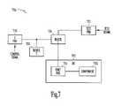
- FIG. 7is a block schematic diagram of an isolation circuit in accordance with a further embodiment of the present invention.
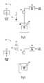
- FIG. 8is a block schematic diagram of an isolation circuit including a conductive jumper to selectively prevent a test pad from being coupled to a part pad in accordance with another embodiment of the present invention.
- FIG. 9is a block schematic diagram of an isolation circuit including an anti-fuse to selectively prevent a test pad from being coupled to a part pad in accordance with an embodiment of the present invention.
- FIG. 10is a block schematic diagram of an isolation circuit in accordance with another embodiment of the present invention.
- FIG. 11is a block schematic diagram of an isolation circuit in accordance with a further embodiment of the present invention.
- FIG. 12is an example of an application of an isolation circuit in accordance with an embodiment of the present invention.
- FIG. 13is another example of an application of an isolation circuit in accordance with an embodiment of the present invention.
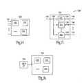
- FIG. 14is a block schematic diagram of a circuit module including microelectronic dies having isolation circuits in accordance with an embodiment of the present invention.
- FIG. 15is a block schematic diagram of a memory module including microelectronic dies with isolation circuits in accordance with an embodiment of the present invention.
- FIG. 16is a block schematic diagram of an electronic system including a isolation circuit in accordance with another embodiment the present invention.
- FIG. 17is a block schematic diagram of a memory system including microelectronic dies with isolation circuits in accordance with an embodiment of the present invention.
- FIG. 18is a block schematic diagram of a computer system including isolation circuits in accordance with an embodiment of the present invention.
- the transistors described hereininclude transistors from bipolar-junction technology (BJT), field effect technology (FET), or complimentary metal-oxide-semiconductor (CMOS) technology.
- a metal-oxide-semiconductor (MOS) transistorincludes a gate, a first node (drain) and a second node (source). Since a MOS transistor is typically a symmetrical device, the true designation of “source” and “drain” is only possible once voltage is impressed on the terminals. The designations of source and drain herein should be interpreted, therefore, in the broadest sense.
- a P-channel MOS transistorcould alternatively be used for an N-channel MOS transistor and vice versa with the polarity of the associated gate voltages merely being reversed. For example, applying a negative gate voltage in the situation of a P-channel MOS transistor to activate the transistor and reversing the polarity to apply a positive gate voltage to activate an N-channel transistor if an N-channel MOS transistor is substituted for a P-channel transistor.
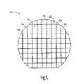
- FIG. 1is a top view of a wafer 100 or substrate containing a plurality of microelectronic or semiconductor dies 102 in accordance with an embodiment of the present invention.
- a die 102is an individual pattern, typically rectangular, on a substrate that contains circuitry to perform a specific function.
- a semiconductor wafer 100will typically contain a repeated pattern of such dies 102 containing the same functionality.
- Die 102can further contain additional circuitry to extend to such complex devices as a monolithic processor with multiple functionality.
- Die 102is typically packaged in a protective casing (not shown) with leads extending therefrom (not shown) providing access to the circuitry of the die 102 for unilateral or bilateral communication and control.
- the dies 102are separated from one another by a scribe line 104 .
- the scribe lines 104can be used to separate each of dies 102 by sawing along the scribe lines 104 .
- Near the edge of the wafer 100are partial or incomplete dies that can be referred to as mutant dies 106 .
- the mutant dieshave typically have insufficient area to contain the repeated circuitry formed on the complete dies 102 .
- FIG. 2is a top view of a portion of a wafer 200 or substrate illustrating an isolation circuit 208 in accordance with an embodiment of the present invention.
- the wafer 200includes a plurality of complete microelectronic dies 202 and mutant dies 206 .
- the dies 202 and 206are separated by scribe lines 204 .
- the wafer 200also includes isolation circuits 208 .
- Each isolation circuit 208can be coupled to a first conductive pad 210 adapted to receive a test signal or other signal or power from a probe of a test system (not shown in FIG. 2 ) or the like.
- a second conductive pad 212 of each the isolation circuit 208can be adapted to receive a control signal from another probe of the test system, and a third conductive pad 214 can be coupled to an associated microelectronic die 202 .
- a device 216can be coupled between the first conductive pad 210 and each third conductive pad 214 to transfer any electrical signals or power at the first conductive pad 210 to the third conductive pad 214 in response to the device receiving a control signal from the second conductive pad 212 .
- the device 216can be an N-channel transistor as shown in FIG.
- the device 216can also be a P-channel transistor, a multiplexor, a conductive jumper, an anti-fuse type device or other fuse type device or a combination of such devices that can be selectively formed or activated to couple the first pad 210 to the third pad 214 or selectively deactivated or open circuited to prevent the first pad 210 from being coupled to the third pad 214 in the event that the particular associated die 202 is defective.
- the first conductive pad 210can be coupled to a plurality of devices 216 as shown in FIG. 2 .
- each of the dies 202can be individually probe tested to determine if any of the dies 202 have certain defects that could adversely impact a signal shared with multiple dies and possibly cause good dies to appear to malfunction or otherwise fail testing. If a defective die 202 is found, the test system can apply a control signal (or not apply a control signal) to the second pad 212 to prevent the device 216 from operating and thus prevent the first conductive pad 210 from being coupled to the third conductive pad 214 and to the microelectronic die 202 .
- each isolation circuit 220is coupled to a first conductive pad 222 adapted to receive a control signal from a probe of a test system (not shown) or the like.
- a second conductive pad 224 of each isolation circuit 220can be adapted to receive a control signal form another probe of the test system, and a third conductive pad 226 can be coupled to an associated microelectronic die 202 .
- a device 228can be coupled between the second conductive pad 224 and the third conductive pad 226 of each isolation circuit 220 to transfer any electrical signals or power at the second conductive pad 224 to the third conductive pad 226 in response to the device 228 receiving a control signal from the first conductive pad 222 .
- the isolation circuit 208can also include a second device 230 connected between the first conductive pad 222 and each of the devices 228 to control the connection or application of the control signal to each of the devices 228 .
- the second device 230can be an anti-fuse type device, a fuse type device, a conductive jumper or a MOS device or a combination thereof. Accordingly, the second devices 230 can be open circuits or closed circuits initially and can be selectively opened or closed to provide flexibility in controlling the application of the control signal to selected dies 202 .
- the second device 230 associated with the defective die 202can be open circuited, if close circuited initially, or left open to prevent a control signal from operating the first device 228 associated with the defective die 202 and allowing the second pad 224 to be coupled to the third pad 226 .
- a third device 232can be coupled to the first pad 222 to control the application of a control signal to a group of devices 228 associated with the particular first pad 222 . In this way application of a signal from the second pad 224 to an entire group of dies 202 , such as a row or column of dies 202 , can be controlled.
- the third device 232can be a fuse type device, anti-fuse type device, MOS device or the like or a combination of such devices.
- the third device 232can be a MOS device to couple the gates of the N-channel transistors 228 to ground to inactivate the transistors 228 and prevent any signal at second pads 224 from passing to the third pads 226 and being applied to the dies 202 in a row or column of dies 202 .
- the first conductive pad 222(or 210 ), the second conductive pad 224 (or 212 ), the first device 228 (or 216 ), and the second and third devices 230 and 232 , if provided, can be formed in the scribe 204 .
- the third conductive pad 226can generally be formed on the die 202 .
- Control signalscan be applied to the first conductive pads 222 and test signals or other signals can be applied to the second conductive pads 224 by probes or pins of a parallel test system (not shown in the Figures) to simultaneously test a plurality of dies 202 on the wafer 200 .
- FIG. 3is a top view of a portion of a wafer 300 or substrate illustrating isolation circuits 308 in accordance with another embodiment of the present invention.
- an isolation circuit 308 Acan be at least partially formed on a mutant die 306 A.
- a first conductive pad 310 A, a second conductive pad 312 A and a device 316 Acan be formed on the mutant die 306 A.
- the device 316 Acan be coupled to a third pad 314 A coupled to a mutant die 306 B.
- the first pad 310 Acan be coupled to other devices 316 C and 316 D formed on dies 302 C and 302 D respectively.
- a second conductive pad 312 C coupled to the device 316 Ccan also be formed on the die 302 C and a second pad 312 D coupled to the device 316 D can be formed on the die 302 D. Accordingly, portions of an isolation circuit 308 can be formed on a mutant die 306 or on the die 302 itself. A good or complete die 302 can also be used or sacrificed, a sacrifice die, to form all or portions of an isolation circuit 308 . A complete isolation circuit 308 E and 308 F are formed on the dies 302 E and 302 F respectively. The isolation circuits 308 E and 308 F can also be coupled to other dies 302 (not shown in FIG. 3 ) to isolate or prevent a signal applied to a second conductive pad 312 associated with one of these other dies 302 from being applied to a third conductive pad 314 that is coupled to a component or circuit formed on one of these other dies 302 .
- FIG. 4is a cross-sectional view of a portion of a semiconductor wafer 400 showing a redistribution layer (RDL) 402 in accordance with an embodiment of the present invention.
- the RDL 402can be any type of conductive material.
- the conductive pads 210 , 212 , 214 and the interconnecting conductive lines or traces in FIG. 2 and the conductive pads 310 , 312 and 314 and the interconnecting conductive lines or traces in FIG. 3can be formed in a RDL, such as the RDL 402 ( FIG. 4 ) to make contact with devices or components, such as device 404 formed on a substrate 406 of the semiconductor wafer 400 .
- FIG. 4As an example in FIG.
- the device or component 404can be a MOS device including a first source/drain region 408 and a second source/drain region 410 formed in the substrate 406 .
- a first layer 412 of conductive material or metallizationcan be formed on a surface 414 of the substrate 406 and selectively patterned to form a gate electrode 416 , a first source/drain electrode 418 in contact with the first source/drain region 408 and a second source/drain electrode 420 in contact with the second source/drain region 410 .
- a layer 422 of insulation materialcan be formed over the first layer 412 of conductive material.
- the RDLcan be formed by forming vias 424 in the layer 422 of insulation material at selected locations to make contact with the underlying devices or components 404 .
- Conductive pads 426can then be formed at each of the vias 424 .
- the conductive pads 426are similar to the conductive pads 210 , 212 and 214 of FIG. 2 and the conductive pads 310 , 312 and 314 of FIG. 3 and provide probe points or locations where electrical signals can be applied or measured during testing operations or for other purposes.
- FIG. 5is a block schematic diagram of an isolation circuit 500 in accordance with an embodiment of the present invention.
- the isolation circuit 500includes a first pad or a control pad 510 adapted to receive a control signal and a second pad 512 adapted to receive a test signal, power or another type signal.
- a third pad or part pad 514can be coupled to a microelectronic die 502 or to a component part 503 formed on the microelectronic die 502 .
- a first device 516couples the test pad 512 to the part pad 514 to transfer the test signal or power to the die 502 or to the component 503 formed on the die 502 in response to the control signal from the control pad 510 .
- the first device 516can be an N-channel MOS device, a P-channel MOS device, a multiplexor, a conductive or metal jumper, a fuse device, such as a fusible link, laser fuse or the like, or an anti-fuse device or a combination of such devices.
- any or all of the pads 510 , 512 and the device 516can be formed in a scribe 104 ( FIG. 1 ), on the die 502 itself, on a mutant die 106 ( FIG. 1 ) or on a sacrifice die 102 ( FIG. 1 ).
- FIG. 6is a block schematic diagram of an isolation circuit 600 in accordance with another embodiment of the present invention.
- the isolation circuit 600includes a test pad 612 , a part pad 614 connected to a microelectronic die 602 or to a component part 603 formed on the die 602 and a first device 616 to couple the test pad 612 to the part pad 614 in response to receiving a control signal.
- the isolation circuit 600can also include a radio frequency identification circuit (RFID) 618 or wireless identification circuit, such as a Bluetooth® type device or the like, coupled to the first device 616 to control operation of the first device 616 .
- RFIDradio frequency identification circuit
- the RFID 618receives a predetermined wireless or RF signal or a coded RF signal and generates a control signal to control operation of the first device 616 in response to the predetermined RF signal. Accordingly, different isolation circuits 600 on a wafer, such as wafer 100 in FIG. 1 , can be selectively controlled to operate (or not operate) the associated device 616 by a wireless signal without having to physically contact the isolation circuit 602 . This process can be useful when the die 600 or wafer is not accessible.
- FIG. 7is a block schematic diagram of an isolation circuit 700 in accordance with a further embodiment of the present invention.
- the isolation circuit 700includes a second device 720 adapted to selectively prevent the first device 716 from operating to prevent the second pad 712 from inadvertently being coupled to the part pad 714 during a predetermined use of the microelectronic die 702 , such as a normally intended use of the die 702 .
- the second device 720can be any device or circuit that can be used to prevent the first device 716 from operating and allowing the test pad 712 to be coupled to the part pad 714 during a predetermined use of the die 702 .
- the test pad 712can present a significant resistive and capacitive load when coupled to the die 702 during operation of the die 702 other than testing. Accordingly, the test pad 712 should be prevented from coupling to the part pad 714 during such operations.
- FIG. 8is a block schematic diagram of an isolation circuit 800 including a conductive jumper 820 , as an example of the second device 720 in FIG. 7 , to selectively prevent a test pad 812 from being coupled to a part pad 814 in accordance with an embodiment of the present invention.
- the isolation circuit 800includes an N-channel transistor 816 , as a example of the first device 716 in FIG. 7 , to couple the test pad 812 to the part pad 814 in response to a control signal from the control pad 810 .
- a conductive jumper 820can be formed to connect the gate of the N-channel transistor 816 to ground potential to prevent the transistor 816 from operating and coupling the test pad 812 to the part pad 814 and thereby adversely effecting operation of the die 802 .
- FIG. 9is a block schematic diagram of an isolation circuit 900 including a circuit 920 with an anti-fuse type device 922 coupled to a supply voltage VCC, as an example of the second device 720 in FIG. 7 , to selectively prevent a test pad 912 from being coupled to a part pad 914 in accordance with an embodiment of the present invention.
- the isolation circuit 900includes a P-channel transistor 916 , as an example of the first device 716 in FIG. 7 , to couple the test pad 912 to the part pad 914 in response to a control signal from the control pad 910 .
- the anti-fuse type device 922can be operated to couple a gate of the P-channel transistor 916 to the supply voltage VCC to prevent the P-channel transistor 916 from operating and coupling the test pad 912 to the part pad 914 and to the die 902 whenever the die 902 is operating under normal conditions.
- FIG. 10is a block schematic diagram of an isolation circuit 1000 in accordance with another embodiment of the present invention.
- the isolation circuit 1000includes a control pad 1010 adapted to receive a control signal and a test pad 1012 adapted to receive a test signal.
- a part pad 1014can be coupled to a microelectronic die 1002 and an N-channel transistor 1016 , as an example of the first device 716 in FIG. 7 , can be provided to couple the test pad 1012 to the part pad 1014 in response to a control signal from the control pad 1010 .
- the isolation circuit 1000further includes a circuit 1020 , as an example of the second device 720 in FIG.
- the circuit 1020can include a second N-channel transistor 1022 with a gate that can be coupled to a supply voltage VCC whenever the die 1002 is in normal operation.
- the supply voltage VCCcauses the transistor 1022 to operate and connect the gate of the transistor 1016 to ground potential to prevent the transistor 1016 from operating and connecting the test pad 1012 to the part pad 1014 during normal operation of the die 1002 .
- the transistor 1022can typically be a weak drive transistor so that a tester drive signal applied to the control pad 1010 can overdrive the transistor 1022 .
- FIG. 10uses N-channel transistors for transistors 1016 and 1022 , P-channel transistors could be used as well with the appropriate voltages or signals being applied to the transistors to prevent the test pad 1012 from being coupled to the part pad 1014 if the die 1002 is defective or during normal operation of the die 1002 .
- FIG. 11is a block diagram of an isolation circuit 1100 including an enable pad 1104 and a disable signal pad 1106 in accordance with an embodiment of the present invention.
- the enable pad 1104 and the disable pad 1106are each coupled to a first device 1116 to control operation of the device 1116 .
- the isolation circuit 1100includes a test pad 1112 adapted to receive a test signal and a part pad 1114 coupled to a microelectronic die 1102 .
- the test pad 1112is coupled to the part pad 1114 by the first device 1116 in response to an enable signal from the enable pad 1104 and the first device 1116 is non-operational or disabled in response to a disable signal from the disable pad 1106 .
- the enable pad 1104can be connected to or disconnected from the first device 1116 by a component 1122 such as a fuse device or an anti-fuse device to provide flexibility in connecting or disconnecting the enable pad 1104 to the first device 1116 .
- the disable pad 1106can be connected to or disconnected from the first device 1116 by a component 1124 such as a fuse device or an anti-fuse device.
- the isolation circuit 1100can also include a second device 1120 to prevent the test pad 1112 from being coupled to the part pad 1114 during normal operation of the die 1102 .
- the first device 1116 and the second device 1120can each be a MOS device, a multiplexor, a conductive or metal jumper, a fuse type device or an anti-fuse type device or a combination of such devices.
- the first device 1116 and the second device 1120can both be formed on the die 1102 .
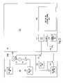
- FIG. 12is an example of an application of an isolation circuit 1200 in accordance with an embodiment of the present invention.
- the isolation circuit 1200includes a first MOS transistor 1202 .
- the first MOS transistor 1202can be an N-channel transistor although a P-channel transistor could be used as well with the appropriate signals being applied to the gate for operation and non-operation of the transistor 1202 .
- a gate of the transistor 1202can be coupled to a RDL enable pad 1203 that can be formed in a redistribution layer (RDL) or upper most conductive layer similar to the RDL 402 shown in FIG. 4 .
- RDLredistribution layer
- One source/drain terminal of the transistor 1202can be coupled to a RDL ground pad 1206 and the other source/drain terminal of the transistor 1202 can be connected to a node 1208 through a fuse device 1210 .
- the fuse device 1210can be formed from metal, polysilicon or other fusible conductive material.
- the RDL enable pad 1203can also be connected to the node 1208 through a fuse device 1212 .
- the node 1208can be connected to a second MOS device 1214 and to a third MOS device 1216 .
- the MOS devices 1214 and 1216are N-channel transistors but could also be P-channel devices.
- One source/drain terminal of the MOS device 1214can be connected to a RDL VCC pad 1218 to receive a supply voltage and the other source/drain terminal of the MOS device 1214 can be connected to a VCC pad 1220 on the die 1222 .
- the MOS device 1214can connect a supply voltage or a power source to the VCC pad 1220 on the die 1222 when the MOS device 1214 is activated or turned on by a control signal applied to the RDL enable pad 1203 .
- the RDL VCC pad 1218can be formed in an RDL in a scribe line 1204 and the VCC pad 1220 can be formed on the die 1222 and in contact therewith.
- One source/drain terminal of the MOS device 1216can be connected to a RDL command and address pad (RDL CMD & ADD) 1224 and the other source/drain of the MOS device 1216 can be connected to command and address pad 1226 formed on the die 1222 .
- RDL CMD & ADDRDL command and address pad
- MOS device 1228can be coupled between the MOS device 1216 and the command and address pad 1226 formed on the die 1222 .
- the MOS device 1228can be an N-channel transistor with a gate electrode connected to an anti-fuse and associated control logic circuitry 1230 to control operation of the MOS device 1228 .
- Anti-fuses and associated control logic circuitry to control operation or blowing of the anti-fuse, such as anti-fuse and associate control logic 1230are known.
- the anti-fuse and associated control logic 1230can provide an AF_CONTROL signal to control operation of the N-channel MOS device 1228 .
- the AF_CONTROL signalcan be translated by the anti-fuse and associated control logic circuitry 1230 to a higher or lower voltage other than a supply voltage VCC to optimize the turning on of the MOS device 1228 .
- the N-channel MOS device 1228will be on or operative in response to the AF_CONTROL signal being high or a logic “1” when the anti-fuse of the anti-fuse and control logic circuitry 1230 is not blown or operated. In this on or operative state, the MOS device 1228 can pass any signals from the MOS device 1216 to the command and address pad 1226 .
- the MOS device 1228will be off or non-operative in response to the AF_CONTROL signal being low or a logic “0” when the anti-fuse of the anti-fuse and control logic 1230 is blown. In this off or non-operative state, the MOS device 1228 isolates the command and address pad 1226 from the capacitance associated with the conductive routing trace between the MOS device 1228 and the MOS device 1216 .
- P-channel MOS devicescould be substituted for N-channel devices with the gate control voltages being reversed or the opposite polarity to control operation of the P-channel MOS devices.
- the isolation circuit 1200is operated by blowing the fuse device 1210 and leaving the fuse device 1212 intact.
- An enable signal applied to the RDL enable pad 1203will turn on or activate the MOS devices 1214 and 1216 .
- the MOS device 1214will transfer any test signal, power or other signal applied to the RDL VCC pad 1218 to the VCC pad 1220 on the die 1222
- the MOS device 1216will transfer any test signal or other signal applied to the RDL command and address pad 1224 to the command and address pad 1226 on the die 1222 .
- the isolation circuit 1200is operated by blowing the fuse device 1212 and leaving the fuse device 1210 intact.
- a high signal or an enable signal applied to the RDL enable pad 1203 by a probe of a parallel test systemcauses the MOS device or transistor 1202 to operate and to connect the RDL ground pad 1206 and ground potential to the MOS devices 1214 and 1216 to prevent them from operating.
- the RDL VCC pad 1218is not coupled to the VCC pad 1220 on the die 1222 and the RDL CMD & ADD pad 1224 are not coupled to the Command & Address pad 1226 on the die 1222 . Therefore, if the die 1222 is defective, the die 1222 can effectively be isolated during WLB, WLT or parallel testing so as to not adversely effect the testing of other dies on a wafer.
- FIG. 13is another example of an application of an isolation circuit 1300 in accordance with an embodiment of the present invention.
- the isolation circuit 1300is similar to the isolation circuit 1200 in FIG. 12 except the second MOS device 1314 coupled between a RDL VCC pad 1318 and a VCC pad 1320 can be formed on the die 1322 rather than in the scribe 1304 as shown in FIG. 12 .
- the third MOS device 1316can also be formed on the die 1322 . If either the second MOS device 1314 or the third MOS device 1316 are formed on the die 1322 , another MOS device 1340 can be formed on the die 1322 and coupled to the node 1308 .
- the MOS device 1340can be an N-channel transistor or the like.
- the gate of the N-channel transistor 1340can be connected to VCC to connect the gates of the second MOS device 1314 and the third MOS device 1316 to ground potential to turn off the second MOS device 1314 and the third MOS device 1316 during a selected operation of the die 1322 , such as normal operation of the die 1322 , and with the RDL removed or sawed off.
- Turning off the second MOS device 1314prevents the RDL VCC pad 1318 from being coupled to the VCC pad 1320 during normal operation of the die 1322 and turning off the third MOS device 1316 prevents the RDL CMD & ADD pad 1324 from being coupled to the Command & Address pad 1326 during normal operation or a predetermined operation of the die 1322 .
- MOS device 1328similar to the MOS device 1228 in FIG. 12 can be coupled between the third MOS device 1316 and the command and address pad 1326 .
- the gate electrode of the MOS device 1328can be coupled to an anti-fuse and associated control logic circuitry 1330 to control operation of the MOS device 1328 .
- the anti-fuse and associated control logic circuitry 1330can be similar to the anti-fuse and associated control logic 1230 in FIG. 12 and can operate in a like manner.
- FIG. 14is a block schematic diagram of a circuit module 1400 including microelectronic dies 1402 with isolation circuits, similar to those previously described in FIGS. 2-13 , in accordance with an embodiment of the present invention.
- two or more dies 1402can be combined, with or without a protective casing, into a circuit module 1400 to enhance or extend the functionality of an individual die 1402 .
- Circuit module 1400can be a combination of dies 1402 representing a variety of functions, or a combination of dies 1402 containing the same functionality.
- Some examples of a circuit module 1400include memory modules, device drivers, power modules, communication modems, processor modules and application-specific modules and can include multi-layer, multi-chip modules.
- Circuit module 1400can be a sub-component of a variety of electronic systems, such as a clock, a television, a cell phone, a personal computer, an automobile, an industrial control system, an aircraft and others. Circuit module 1400 will have a variety of leads 1410 extending therefrom providing unilateral or bilateral communication and control.
- FIG. 15shows one embodiment of a circuit module as a memory module 1500 including isolation circuits similar to those previously described with reference to FIGS. 2-13 .
- Memory module 1500generally depicts a Single In-line Memory Module (SIMM) or Dual In-line Memory Module (DIMM).
- SIMM or DIMMcan generally be a printed circuit board (PCB) or other support containing a series of memory devices. While a SIMM will have a single in-line set of contacts or leads, a DIMM will have a set of leads on each side of the support with each set representing separate I/O signals.
- Memory module 1500contains multiple memory devices 1510 contained on support 1515 , the number depending upon the desired bus width and the desire for parity. Memory module 1500 can contain memory devices 1510 on both sides of support 1515 .
- Memory module 1500accepts a command signal from an external controller (not shown) on a command link 1520 and provides for data input and data output on data links 1530 .
- the command link 1520 and data links 1530are connected to leads 1540 extending from the support 1515 .
- Leads 1540are shown for conceptual purposes and are not limited to the positions shown in FIG. 15 .
- FIG. 16shows an electronic system 1600 containing one or more circuit modules 1602 similar to circuit module 1500 ( FIG. 15 ) and including isolation circuits, such as the isolation circuit 1200 of the present invention.
- Electronic system 1600generally contains a user interface 1610 .
- User interface 1610provides a user of the electronic system 1600 with some form of control or observation of the results of the electronic system 1600 .
- Some examples of user interface 1610include the keyboard, pointing device, monitor and printer of a personal computer; the tuning dial, display and speakers of a radio; the ignition switch and gas pedal of an automobile; and the card reader, keypad, display and currency dispenser of an automated teller machine.
- User interface 1610can further describe access ports provided to electronic system 1600 .
- Access portsare used to connect an electronic system to the more tangible user interface components previously exemplified.
- One or more circuit modules 1602can be a processor providing some form of manipulation, control or direction of inputs from or outputs to user interface 1610 , or of other information either preprogrammed into, or otherwise provided to, electronic system 1600 .
- electronic system 1600will often contain certain mechanical components (not shown) in addition to the circuit modules 1602 and user interface 1610 . It will be appreciated that the one or more circuit modules 1602 in electronic system 1600 can be replaced by a single integrated circuit.
- electronic system 1600can be a sub-component of a larger electronic system.
- FIG. 17shows one embodiment of an electronic system as memory system 1700 .
- Memory system 1700contains one or more memory modules 1702 similar to memory modules 1500 in FIG. 15 and including an isolation circuits, such as isolation circuit 1200 in accordance with the present invention.
- a memory controller 1710provides and controls a bidirectional interface between memory system 1700 and an external system bus 1720 .
- Memory system 1700accepts a command signal from the external bus 1720 and relays it to the one or more memory modules 1704 on a command link 1730 .
- Memory system 1700provides for data input and data output between the one or more memory modules 1704 and external system bus 1720 on data links 1740 .
- FIG. 18shows a further embodiment of an electronic system as a computer system 1800 .
- Computer system 1800contains a processor 1810 and a memory system 1802 similar to memory system 1700 of FIG. 17 .
- the processor 1810 and the memory system 1802can be housed in a computer unit 1805 .
- Computer system 1800is but one example of an electronic system containing another electronic system, i.e. memory system 1802 .
- the processor 1810 and the memory system 1802can include isolation circuits in accordance with the present invention, such as the isolation circuit 1200 in FIG. 12 .
- Computer system 1800optionally contains user interface components. Depicted in FIG. 18 are a keyboard 1820 , a pointing device 1830 , a monitor 1840 , a printer 1850 and a bulk storage device 1860 .
- processor 1810 and the memory system 1802 of the computer system 1800can be incorporated on a single integrated circuit and can use the isolation circuits of the present invention.
- the present inventionthus provides a circuit or device to isolate a defective die to prevent a shared signal from being impacted by the defective die and thereby adversely effecting the operation or testing of other dies to which the shared signal is applied. Additionally, the present invention provides a circuit or device to prevent a test pad or other type pad from being coupled to an associated microelectronic die during normal operation of the die or during operation of the die other than when the pad is needed to apply a test signal or another signal. Further, the present invention provides a method for testing multiple dies on a wafer where a defective die cannot adversely effect the testing of other dies sharing a common signal.
Landscapes
- Engineering & Computer Science (AREA)
- Computer Hardware Design (AREA)
- Microelectronics & Electronic Packaging (AREA)
- General Engineering & Computer Science (AREA)
- Physics & Mathematics (AREA)
- General Physics & Mathematics (AREA)
- Semiconductor Integrated Circuits (AREA)
- Design And Manufacture Of Integrated Circuits (AREA)
- Testing Or Measuring Of Semiconductors Or The Like (AREA)
Abstract
Description
- This application is a Continuation of U.S. application Ser. No. 11/338,066, filed Jan. 24, 2006 which is a Divisional of U.S. application Ser. No. 10/176,015, filed Jun. 20, 2002, now issued as U.S. Pat. No. 7,026,646 which are incorporated herein their entirety by reference.
- The present application is related to U.S. application Ser. No. 10/176,330, filed Jun. 20, 2002, now U.S. Pat. No. 6,967,348, and is assigned to the assignee as the present application and is incorporated herein in its entirety by reference.
- The present invention relates generally to microelectronic dies, semiconductor chips and the like, and more particularly to an isolation circuit for use with a microelectronic die.
- In semiconductor wafers including microelectronic dies formed on the wafers and the like, an electrical signal can be transmitted or shared from one component part or die to another. This can be the case in testing a wafer when a test signal can be sent to multiple different dies. One problem with sharing an electrical signal from one part or die to another is that a malfunction or defect in any of the dies can adversely effect the electrical signal being shared and cause the remaining dies to malfunction or appear to fail the test when the dies may actually be good.
- One example where electrical signals are shared by a plurality of different parts or dies is in a parallel test system for Wafer Level Testing (WLT). In WLT, multiple dies on a wafer can be evaluated simultaneously. Prior to WLT, each of the dies on a wafer can be individually tested by probe testing or by a similar procedure to determine if any of the dies have certain defects. After probe testing, several predetermined electrical signals can be applied to contact pads formed on the wafer to more efficiently test multiple dies simultaneously. If one or more of the dies in a group being tested together are defective, the integrity of the shared electrical signal can be impacted such that potentially all of the dies sharing the signal can fail the test. There can also be uses other than testing when electrical signals are shared and one or more defective parts or dies can adversely effect the electrical signals and consequently the performance of a device or system incorporating the dies.
- Electrical signals such as the shared electrical signals can be applied to a die by a conductive pad formed on the die or wafer. For example, at least one test pad can be formed in association with each die for applying test signals during WLT. The different test pads that share the test signal can be interconnected by conductive lines or traces. During normal operation of the die, a test pad and associated interconnect lines or traces can become inadvertently coupled to an associated die or remnants of a test pad and associated interconnect lines after the dies are separated from the wafer can become inadvertently coupled to the die. The test pad and interconnecting lines can present a substantial capacitive and resistive load coupled to the die that can adversely effect performance of the die.
- Accordingly, for the reasons stated above, and for other reasons that will become apparent upon reading and understanding the present specification, there is a need for a circuit or device to isolate a defective die to prevent a shared signal from being impacted by the defective die and thereby adversely effecting the operation or testing of other dies to which the shared signal is applied. Additionally, there is a need for a circuit or device to prevent a test pad or other type pad from being coupled to an associated microelectronic die during normal operation of the die or during operation of the die other than when the pad is needed to apply a test signal or another signal. Further, there is a need for a method of testing multiple dies on a wafer where a defective die cannot adversely effect the testing of other dies sharing a common signal.
- The above mentioned problems with defective microelectronic dies are addressed by the present invention and will be understood by reading and studying the following specification. Isolation circuits, microelectronic dies, semiconductor wafers and systems are provided by the present invention that isolate a defective die and thereby prevent a shared signal from being impacted by the defective die and prevent the defective die from effecting the operation or testing of other dies to which the shared signal is applied. The present invention also provides a circuit or device to prevent a test pad or other pad from being coupled to an associated microelectronic die during normal operation of the die or during operation of the die other than when the pad is needed to apply a signal.
- In accordance with an embodiment of the present invention, an isolation circuit includes a first pad adapted to receive a control signal and a second pad adapted to receive another signal, such as a test signal. A third pad is coupled to a microelectronic die and a device is adapted to transfer the other signal from the second pad to the third pad in response to the control signal.
- In accordance with another embodiment of the present invention, an isolation circuit includes a first pad adapted to receive a control signal and a second pad adapted to receive another signal. A third pad is coupled to a microelectronic die. A first device is adapted to transfer the other signal from the second pad to the third pad in response to the control signal. A second device is adapted to selectively prevent the second pad from being coupled to the third pad during a predetermined use or normal use of the microelectronic die.
- In accordance with another embodiment of the present invention, an electronic system includes a processor and a memory system coupled to the processor, wherein at least one of the processor and the memory system are formed on a microelectronic die including an isolation circuit. The isolation circuit includes a first pad adapted to receive a control signal and a second pad adapted to receive another signal. A third pad is coupled to one of the processor or the memory system and a device is adapted to transfer the other signal from the second pad to the third pad in response to the control signal.
- In accordance with another embodiment of the present invention, a method comprises: determining if any microelectronic dies of a plurality of microelectronic dies formed on a semiconductor wafer are defective; applying a test signal to a test pad associated with each of the microelectronic dies; operating a device associated with each microelectronic die to couple the test pad to a part pad if the microelectronic die is good, wherein the part pad is connected to the microelectronic die; and preventing the test signal from being applied to the microelectronic die if the die is defective.
- These and other embodiments, aspects, advantages and features of the present invention will be set forth in part in the description which follows, and in part will become apparent to those skilled in the art by reference to the following description of the invention and referenced drawings or by practice of the invention. The aspects, advantages, and features of the invention are realized and attained by means of the instrumentalities, procedures, and combinations particularly pointed out in the appended claims.
- In the drawings, like numerals describe substantially similar components throughout the several views. Like numerals having different letter suffixes or primed (X′) represent different occurrences of substantially similar components.
FIG. 1 is a top view of a wafer or substrate containing microelectronic or semiconductor dies in accordance with an embodiment of the present invention.FIG. 2 is a top view of a portion of a wafer or substrate illustrating an isolation circuit in accordance with an embodiment of the present invention.FIG. 3 is a top view of a portion of a wafer or substrate illustrating an isolation circuit in accordance with another embodiment of the present invention.FIG. 4 is a cross-sectional view of a wafer or substrate showing a redistribution layer (RDL) in accordance with an embodiment of the present invention.FIG. 5 is a block schematic diagram of an isolation circuit in accordance with an embodiment of the present invention.FIG. 6 is a block schematic diagram of an isolation circuit in accordance with another embodiment the present invention.FIG. 7 is a block schematic diagram of an isolation circuit in accordance with a further embodiment of the present invention.FIG. 8 is a block schematic diagram of an isolation circuit including a conductive jumper to selectively prevent a test pad from being coupled to a part pad in accordance with another embodiment of the present invention.FIG. 9 is a block schematic diagram of an isolation circuit including an anti-fuse to selectively prevent a test pad from being coupled to a part pad in accordance with an embodiment of the present invention.FIG. 10 is a block schematic diagram of an isolation circuit in accordance with another embodiment of the present invention.FIG. 11 is a block schematic diagram of an isolation circuit in accordance with a further embodiment of the present invention.FIG. 12 is an example of an application of an isolation circuit in accordance with an embodiment of the present invention.FIG. 13 is another example of an application of an isolation circuit in accordance with an embodiment of the present invention.FIG. 14 is a block schematic diagram of a circuit module including microelectronic dies having isolation circuits in accordance with an embodiment of the present invention.FIG. 15 is a block schematic diagram of a memory module including microelectronic dies with isolation circuits in accordance with an embodiment of the present invention.FIG. 16 is a block schematic diagram of an electronic system including a isolation circuit in accordance with another embodiment the present invention.FIG. 17 is a block schematic diagram of a memory system including microelectronic dies with isolation circuits in accordance with an embodiment of the present invention.FIG. 18 is a block schematic diagram of a computer system including isolation circuits in accordance with an embodiment of the present invention.- In the following detailed description of the preferred embodiments, reference is made to the accompanying drawings which form a part hereof, and in which is shown by way of illustration specific embodiments in which the invention may be practiced. These embodiments are described in sufficient detail to enable those skilled in the art to practice the invention, and it is to be understood that other embodiments can be utilized and that process or mechanical changes may be made without departing from the scope of the present invention. The terms wafer and substrate used in the following description include any base semiconductor structure. Both are to be understood as including silicon-on-sapphire (SOS) technology, silicon-on-insulator (SOI) technology, thin film transistor (TFT) technology, doped and undoped semiconductors, epitaxial layers of a silicon supported by a base semiconductor, as well as other semiconductor support structures well known to one skilled in the art. Furthermore, when reference is made to a wafer or substrate in the following description, previous process operations may have been utilized to form regions/junctions in the base semiconductor structure. The following detailed description is, therefore, not to be taken in a limiting sense, and the scope of the present invention is defined only by the appended claims.
- The transistors described herein include transistors from bipolar-junction technology (BJT), field effect technology (FET), or complimentary metal-oxide-semiconductor (CMOS) technology. A metal-oxide-semiconductor (MOS) transistor includes a gate, a first node (drain) and a second node (source). Since a MOS transistor is typically a symmetrical device, the true designation of “source” and “drain” is only possible once voltage is impressed on the terminals. The designations of source and drain herein should be interpreted, therefore, in the broadest sense. It should also be noted that a P-channel MOS transistor could alternatively be used for an N-channel MOS transistor and vice versa with the polarity of the associated gate voltages merely being reversed. For example, applying a negative gate voltage in the situation of a P-channel MOS transistor to activate the transistor and reversing the polarity to apply a positive gate voltage to activate an N-channel transistor if an N-channel MOS transistor is substituted for a P-channel transistor.
FIG. 1 is a top view of awafer 100 or substrate containing a plurality of microelectronic or semiconductor dies102 in accordance with an embodiment of the present invention. Adie 102 is an individual pattern, typically rectangular, on a substrate that contains circuitry to perform a specific function. Asemiconductor wafer 100 will typically contain a repeated pattern of such dies102 containing the same functionality. Die102 can further contain additional circuitry to extend to such complex devices as a monolithic processor with multiple functionality.Die 102 is typically packaged in a protective casing (not shown) with leads extending therefrom (not shown) providing access to the circuitry of thedie 102 for unilateral or bilateral communication and control. The dies102 are separated from one another by ascribe line 104. The scribe lines104 can be used to separate each of dies102 by sawing along the scribe lines104. Near the edge of thewafer 100 are partial or incomplete dies that can be referred to as mutant dies106. The mutant dies have typically have insufficient area to contain the repeated circuitry formed on the complete dies102.FIG. 2 is a top view of a portion of awafer 200 or substrate illustrating anisolation circuit 208 in accordance with an embodiment of the present invention. Thewafer 200 includes a plurality of complete microelectronic dies202 and mutant dies206. The dies202 and206 are separated byscribe lines 204. Thewafer 200 also includesisolation circuits 208. Eachisolation circuit 208 can be coupled to a firstconductive pad 210 adapted to receive a test signal or other signal or power from a probe of a test system (not shown inFIG. 2 ) or the like. A secondconductive pad 212 of each theisolation circuit 208 can be adapted to receive a control signal from another probe of the test system, and a thirdconductive pad 214 can be coupled to an associated microelectronic die202. Adevice 216 can be coupled between the firstconductive pad 210 and each thirdconductive pad 214 to transfer any electrical signals or power at the firstconductive pad 210 to the thirdconductive pad 214 in response to the device receiving a control signal from the secondconductive pad 212. Thedevice 216 can be an N-channel transistor as shown inFIG. 2 or thedevice 216 can also be a P-channel transistor, a multiplexor, a conductive jumper, an anti-fuse type device or other fuse type device or a combination of such devices that can be selectively formed or activated to couple thefirst pad 210 to thethird pad 214 or selectively deactivated or open circuited to prevent thefirst pad 210 from being coupled to thethird pad 214 in the event that the particular associated die202 is defective.- In parallel testing multiple dies202 on a
wafer 200 or wafer level testing (WLT), the firstconductive pad 210 can be coupled to a plurality ofdevices 216 as shown inFIG. 2 . Prior to WLT or parallel testing, each of the dies202 can be individually probe tested to determine if any of the dies202 have certain defects that could adversely impact a signal shared with multiple dies and possibly cause good dies to appear to malfunction or otherwise fail testing. If adefective die 202 is found, the test system can apply a control signal (or not apply a control signal) to thesecond pad 212 to prevent thedevice 216 from operating and thus prevent the firstconductive pad 210 from being coupled to the thirdconductive pad 214 and to themicroelectronic die 202. - Another embodiment of the present invention is shown with respect to a
second row 218 of dies202 inFIG. 2 . This other embodiment and the embodiment described above with respect to thefirst row 219 of dies would not necessarily be used in practice together on thesame wafer 200 but typically one embodiment or the other can be used through out anentire wafer 200. In this embodiment, eachisolation circuit 220 is coupled to a first conductive pad222 adapted to receive a control signal from a probe of a test system (not shown) or the like. A secondconductive pad 224 of eachisolation circuit 220 can be adapted to receive a control signal form another probe of the test system, and a thirdconductive pad 226 can be coupled to an associated microelectronic die202. Adevice 228 can be coupled between the secondconductive pad 224 and the thirdconductive pad 226 of eachisolation circuit 220 to transfer any electrical signals or power at the secondconductive pad 224 to the thirdconductive pad 226 in response to thedevice 228 receiving a control signal from the first conductive pad222. - The
isolation circuit 208 can also include asecond device 230 connected between the first conductive pad222 and each of thedevices 228 to control the connection or application of the control signal to each of thedevices 228. Thesecond device 230 can be an anti-fuse type device, a fuse type device, a conductive jumper or a MOS device or a combination thereof. Accordingly, thesecond devices 230 can be open circuits or closed circuits initially and can be selectively opened or closed to provide flexibility in controlling the application of the control signal to selected dies202. For example, if adie 202 is determined to be defective during a probing operation of thewafer 200, then thesecond device 230 associated with thedefective die 202 can be open circuited, if close circuited initially, or left open to prevent a control signal from operating thefirst device 228 associated with thedefective die 202 and allowing thesecond pad 224 to be coupled to thethird pad 226. - In a further embodiment of the present invention, a
third device 232 can be coupled to the first pad222 to control the application of a control signal to a group ofdevices 228 associated with the particular first pad222. In this way application of a signal from thesecond pad 224 to an entire group of dies202, such as a row or column of dies202, can be controlled. Thethird device 232 can be a fuse type device, anti-fuse type device, MOS device or the like or a combination of such devices. For example, thethird device 232 can be a MOS device to couple the gates of the N-channel transistors 228 to ground to inactivate thetransistors 228 and prevent any signal atsecond pads 224 from passing to thethird pads 226 and being applied to the dies202 in a row or column of dies202. - As shown in
FIG. 2 , the first conductive pad222 (or210), the second conductive pad224 (or212), the first device228 (or216), and the second andthird devices scribe 204. The thirdconductive pad 226 can generally be formed on thedie 202. - Control signals can be applied to the first conductive pads222 and test signals or other signals can be applied to the second
conductive pads 224 by probes or pins of a parallel test system (not shown in the Figures) to simultaneously test a plurality of dies202 on thewafer 200. FIG. 3 is a top view of a portion of awafer 300 or substrate illustrating isolation circuits308 in accordance with another embodiment of the present invention. In this embodiment, anisolation circuit 308A can be at least partially formed on a mutant die306A. A firstconductive pad 310A, a secondconductive pad 312A and adevice 316A can be formed on the mutant die306A. Thedevice 316A can be coupled to athird pad 314A coupled to amutant die 306B. Thefirst pad 310A can be coupled toother devices conductive pad 312C coupled to thedevice 316C can also be formed on thedie 302C and asecond pad 312D coupled to thedevice 316D can be formed on thedie 302D. Accordingly, portions of an isolation circuit308 can be formed on a mutant die306 or on the die302 itself. A good or complete die302 can also be used or sacrificed, a sacrifice die, to form all or portions of an isolation circuit308. Acomplete isolation circuit isolation circuits FIG. 3 ) to isolate or prevent a signal applied to a second conductive pad312 associated with one of these other dies302 from being applied to a third conductive pad314 that is coupled to a component or circuit formed on one of these other dies302.FIG. 4 is a cross-sectional view of a portion of asemiconductor wafer 400 showing a redistribution layer (RDL)402 in accordance with an embodiment of the present invention. TheRDL 402 can be any type of conductive material. Theconductive pads FIG. 2 and the conductive pads310,312 and314 and the interconnecting conductive lines or traces inFIG. 3 can be formed in a RDL, such as the RDL402 (FIG. 4 ) to make contact with devices or components, such asdevice 404 formed on asubstrate 406 of thesemiconductor wafer 400. As an example inFIG. 4 , the device orcomponent 404 can be a MOS device including a first source/drain region 408 and a second source/drain region 410 formed in thesubstrate 406. Afirst layer 412 of conductive material or metallization can be formed on asurface 414 of thesubstrate 406 and selectively patterned to form agate electrode 416, a first source/drain electrode 418 in contact with the first source/drain region 408 and a second source/drain electrode 420 in contact with the second source/drain region 410. Alayer 422 of insulation material can be formed over thefirst layer 412 of conductive material. The RDL can be formed by formingvias 424 in thelayer 422 of insulation material at selected locations to make contact with the underlying devices orcomponents 404.Conductive pads 426 can then be formed at each of thevias 424. Theconductive pads 426 are similar to theconductive pads FIG. 2 and the conductive pads310,312 and314 ofFIG. 3 and provide probe points or locations where electrical signals can be applied or measured during testing operations or for other purposes.FIG. 5 is a block schematic diagram of anisolation circuit 500 in accordance with an embodiment of the present invention. Theisolation circuit 500 includes a first pad or acontrol pad 510 adapted to receive a control signal and asecond pad 512 adapted to receive a test signal, power or another type signal. A third pad orpart pad 514 can be coupled to amicroelectronic die 502 or to acomponent part 503 formed on themicroelectronic die 502. Afirst device 516 couples thetest pad 512 to thepart pad 514 to transfer the test signal or power to the die502 or to thecomponent 503 formed on thedie 502 in response to the control signal from thecontrol pad 510. Thefirst device 516 can be an N-channel MOS device, a P-channel MOS device, a multiplexor, a conductive or metal jumper, a fuse device, such as a fusible link, laser fuse or the like, or an anti-fuse device or a combination of such devices. As previously discussed with respect toFIGS. 2 and 3 , any or all of thepads device 516 can be formed in a scribe104 (FIG. 1 ), on thedie 502 itself, on a mutant die106 (FIG. 1 ) or on a sacrifice die102 (FIG. 1 ).FIG. 6 is a block schematic diagram of anisolation circuit 600 in accordance with another embodiment of the present invention. Theisolation circuit 600 includes atest pad 612, apart pad 614 connected to amicroelectronic die 602 or to acomponent part 603 formed on thedie 602 and afirst device 616 to couple thetest pad 612 to thepart pad 614 in response to receiving a control signal. Theisolation circuit 600 can also include a radio frequency identification circuit (RFID)618 or wireless identification circuit, such as a Bluetooth® type device or the like, coupled to thefirst device 616 to control operation of thefirst device 616. The RFID618 receives a predetermined wireless or RF signal or a coded RF signal and generates a control signal to control operation of thefirst device 616 in response to the predetermined RF signal. Accordingly,different isolation circuits 600 on a wafer, such aswafer 100 inFIG. 1 , can be selectively controlled to operate (or not operate) the associateddevice 616 by a wireless signal without having to physically contact theisolation circuit 602. This process can be useful when thedie 600 or wafer is not accessible.FIG. 7 is a block schematic diagram of anisolation circuit 700 in accordance with a further embodiment of the present invention. Theisolation circuit 700 includes asecond device 720 adapted to selectively prevent thefirst device 716 from operating to prevent thesecond pad 712 from inadvertently being coupled to thepart pad 714 during a predetermined use of themicroelectronic die 702, such as a normally intended use of thedie 702. Thesecond device 720 can be any device or circuit that can be used to prevent thefirst device 716 from operating and allowing thetest pad 712 to be coupled to thepart pad 714 during a predetermined use of thedie 702. Thetest pad 712 can present a significant resistive and capacitive load when coupled to thedie 702 during operation of thedie 702 other than testing. Accordingly, thetest pad 712 should be prevented from coupling to thepart pad 714 during such operations.FIG. 8 is a block schematic diagram of anisolation circuit 800 including aconductive jumper 820, as an example of thesecond device 720 inFIG. 7 , to selectively prevent atest pad 812 from being coupled to apart pad 814 in accordance with an embodiment of the present invention. Theisolation circuit 800 includes an N-channel transistor 816, as a example of thefirst device 716 inFIG. 7 , to couple thetest pad 812 to thepart pad 814 in response to a control signal from thecontrol pad 810. After testing or before normal operation of thedie 802, aconductive jumper 820 can be formed to connect the gate of the N-channel transistor 816 to ground potential to prevent thetransistor 816 from operating and coupling thetest pad 812 to thepart pad 814 and thereby adversely effecting operation of thedie 802.FIG. 9 is a block schematic diagram of anisolation circuit 900 including acircuit 920 with ananti-fuse type device 922 coupled to a supply voltage VCC, as an example of thesecond device 720 inFIG. 7 , to selectively prevent atest pad 912 from being coupled to apart pad 914 in accordance with an embodiment of the present invention. Theisolation circuit 900 includes a P-channel transistor 916, as an example of thefirst device 716 inFIG. 7 , to couple thetest pad 912 to thepart pad 914 in response to a control signal from thecontrol pad 910. After thedie 902 is tested or before normal operation of thedie 902, theanti-fuse type device 922 can be operated to couple a gate of the P-channel transistor 916 to the supply voltage VCC to prevent the P-channel transistor 916 from operating and coupling thetest pad 912 to thepart pad 914 and to the die902 whenever thedie 902 is operating under normal conditions.FIG. 10 is a block schematic diagram of anisolation circuit 1000 in accordance with another embodiment of the present invention. Theisolation circuit 1000 includes acontrol pad 1010 adapted to receive a control signal and atest pad 1012 adapted to receive a test signal. Apart pad 1014 can be coupled to amicroelectronic die 1002 and an N-channel transistor 1016, as an example of thefirst device 716 inFIG. 7 , can be provided to couple thetest pad 1012 to thepart pad 1014 in response to a control signal from thecontrol pad 1010. Theisolation circuit 1000 further includes acircuit 1020, as an example of thesecond device 720 inFIG. 7 , to couple a gate of the N-channel transistor 1016 to ground potential or any potential to prevent thetransistor 1016 from operating and coupling thetest pad 1012 to thepart pad 1014 during normal operations of thedie 1002. Thecircuit 1020 can include a second N-channel transistor 1022 with a gate that can be coupled to a supply voltage VCC whenever thedie 1002 is in normal operation. The supply voltage VCC causes thetransistor 1022 to operate and connect the gate of thetransistor 1016 to ground potential to prevent thetransistor 1016 from operating and connecting thetest pad 1012 to thepart pad 1014 during normal operation of thedie 1002. Thetransistor 1022 can typically be a weak drive transistor so that a tester drive signal applied to thecontrol pad 1010 can overdrive thetransistor 1022.- While the embodiment shown in
FIG. 10 uses N-channel transistors fortransistors test pad 1012 from being coupled to thepart pad 1014 if thedie 1002 is defective or during normal operation of thedie 1002. FIG. 11 is a block diagram of anisolation circuit 1100 including an enablepad 1104 and a disablesignal pad 1106 in accordance with an embodiment of the present invention. The enablepad 1104 and the disablepad 1106 are each coupled to afirst device 1116 to control operation of thedevice 1116. Theisolation circuit 1100 includes atest pad 1112 adapted to receive a test signal and apart pad 1114 coupled to amicroelectronic die 1102. Thetest pad 1112 is coupled to thepart pad 1114 by thefirst device 1116 in response to an enable signal from theenable pad 1104 and thefirst device 1116 is non-operational or disabled in response to a disable signal from the disablepad 1106. The enablepad 1104 can be connected to or disconnected from thefirst device 1116 by acomponent 1122 such as a fuse device or an anti-fuse device to provide flexibility in connecting or disconnecting theenable pad 1104 to thefirst device 1116. Similarly, the disablepad 1106 can be connected to or disconnected from thefirst device 1116 by acomponent 1124 such as a fuse device or an anti-fuse device.- The
isolation circuit 1100 can also include asecond device 1120 to prevent thetest pad 1112 from being coupled to thepart pad 1114 during normal operation of thedie 1102. As previously discussed, thefirst device 1116 and thesecond device 1120 can each be a MOS device, a multiplexor, a conductive or metal jumper, a fuse type device or an anti-fuse type device or a combination of such devices. Thefirst device 1116 and thesecond device 1120 can both be formed on thedie 1102. FIG. 12 is an example of an application of anisolation circuit 1200 in accordance with an embodiment of the present invention. Theisolation circuit 1200 includes afirst MOS transistor 1202. In the example shown, thefirst MOS transistor 1202 can be an N-channel transistor although a P-channel transistor could be used as well with the appropriate signals being applied to the gate for operation and non-operation of thetransistor 1202. A gate of thetransistor 1202 can be coupled to a RDL enablepad 1203 that can be formed in a redistribution layer (RDL) or upper most conductive layer similar to theRDL 402 shown inFIG. 4 . One source/drain terminal of thetransistor 1202 can be coupled to aRDL ground pad 1206 and the other source/drain terminal of thetransistor 1202 can be connected to anode 1208 through afuse device 1210. Thefuse device 1210 can be formed from metal, polysilicon or other fusible conductive material. The RDL enablepad 1203 can also be connected to thenode 1208 through afuse device 1212. Thenode 1208 can be connected to asecond MOS device 1214 and to athird MOS device 1216. In the example ofFIG. 12 , theMOS devices MOS device 1214 can be connected to aRDL VCC pad 1218 to receive a supply voltage and the other source/drain terminal of theMOS device 1214 can be connected to aVCC pad 1220 on thedie 1222. TheMOS device 1214 can connect a supply voltage or a power source to theVCC pad 1220 on thedie 1222 when theMOS device 1214 is activated or turned on by a control signal applied to the RDL enablepad 1203. TheRDL VCC pad 1218 can be formed in an RDL in ascribe line 1204 and theVCC pad 1220 can be formed on thedie 1222 and in contact therewith. One source/drain terminal of theMOS device 1216 can be connected to a RDL command and address pad (RDL CMD & ADD)1224 and the other source/drain of theMOS device 1216 can be connected to command andaddress pad 1226 formed on thedie 1222.- Another
MOS device 1228 can be coupled between theMOS device 1216 and the command andaddress pad 1226 formed on thedie 1222. TheMOS device 1228 can be an N-channel transistor with a gate electrode connected to an anti-fuse and associatedcontrol logic circuitry 1230 to control operation of theMOS device 1228. Anti-fuses and associated control logic circuitry to control operation or blowing of the anti-fuse, such as anti-fuse andassociate control logic 1230, are known. The anti-fuse and associatedcontrol logic 1230 can provide an AF_CONTROL signal to control operation of the N-channel MOS device 1228. The AF_CONTROL signal can be translated by the anti-fuse and associatedcontrol logic circuitry 1230 to a higher or lower voltage other than a supply voltage VCC to optimize the turning on of theMOS device 1228. The N-channel MOS device 1228 will be on or operative in response to the AF_CONTROL signal being high or a logic “1” when the anti-fuse of the anti-fuse and controllogic circuitry 1230 is not blown or operated. In this on or operative state, theMOS device 1228 can pass any signals from theMOS device 1216 to the command andaddress pad 1226. TheMOS device 1228 will be off or non-operative in response to the AF_CONTROL signal being low or a logic “0” when the anti-fuse of the anti-fuse andcontrol logic 1230 is blown. In this off or non-operative state, theMOS device 1228 isolates the command andaddress pad 1226 from the capacitance associated with the conductive routing trace between theMOS device 1228 and theMOS device 1216. Those skilled in the art will recognize that P-channel MOS devices could be substituted for N-channel devices with the gate control voltages being reversed or the opposite polarity to control operation of the P-channel MOS devices. - If the
die 1222 is found to be good during a probe operation to evaluate theindividual die 1222 prior to parallel testing, WLT or wafer level burn-in (WLB), theisolation circuit 1200 is operated by blowing thefuse device 1210 and leaving thefuse device 1212 intact. An enable signal applied to the RDL enablepad 1203 will turn on or activate theMOS devices MOS device 1214 will transfer any test signal, power or other signal applied to theRDL VCC pad 1218 to theVCC pad 1220 on thedie 1222, and theMOS device 1216 will transfer any test signal or other signal applied to the RDL command andaddress pad 1224 to the command andaddress pad 1226 on thedie 1222. - If the
die 1222 is found to be defective during a probe operation to evaluate theindividual die 1222 prior to parallel testing or WLT or WLB, theisolation circuit 1200 is operated by blowing thefuse device 1212 and leaving thefuse device 1210 intact. A high signal or an enable signal applied to the RDL enablepad 1203 by a probe of a parallel test system causes the MOS device ortransistor 1202 to operate and to connect theRDL ground pad 1206 and ground potential to theMOS devices RDL VCC pad 1218 is not coupled to theVCC pad 1220 on thedie 1222 and the RDL CMD &ADD pad 1224 are not coupled to the Command &Address pad 1226 on thedie 1222. Therefore, if thedie 1222 is defective, thedie 1222 can effectively be isolated during WLB, WLT or parallel testing so as to not adversely effect the testing of other dies on a wafer. FIG. 13 is another example of an application of anisolation circuit 1300 in accordance with an embodiment of the present invention. Theisolation circuit 1300 is similar to theisolation circuit 1200 inFIG. 12 except thesecond MOS device 1314 coupled between aRDL VCC pad 1318 and aVCC pad 1320 can be formed on thedie 1322 rather than in thescribe 1304 as shown inFIG. 12 . Thethird MOS device 1316 can also be formed on thedie 1322. If either thesecond MOS device 1314 or thethird MOS device 1316 are formed on thedie 1322, anotherMOS device 1340 can be formed on thedie 1322 and coupled to thenode 1308. In the example shown inFIG. 13 , theMOS device 1340 can be an N-channel transistor or the like. The gate of the N-channel transistor 1340 can be connected to VCC to connect the gates of thesecond MOS device 1314 and thethird MOS device 1316 to ground potential to turn off thesecond MOS device 1314 and thethird MOS device 1316 during a selected operation of thedie 1322, such as normal operation of thedie 1322, and with the RDL removed or sawed off. Turning off thesecond MOS device 1314 prevents theRDL VCC pad 1318 from being coupled to theVCC pad 1320 during normal operation of thedie 1322 and turning off thethird MOS device 1316 prevents the RDL CMD &ADD pad 1324 from being coupled to the Command &Address pad 1326 during normal operation or a predetermined operation of thedie 1322.- Another
MOS device 1328 similar to theMOS device 1228 inFIG. 12 can be coupled between thethird MOS device 1316 and the command andaddress pad 1326. The gate electrode of theMOS device 1328 can be coupled to an anti-fuse and associatedcontrol logic circuitry 1330 to control operation of theMOS device 1328. The anti-fuse and associatedcontrol logic circuitry 1330 can be similar to the anti-fuse and associatedcontrol logic 1230 inFIG. 12 and can operate in a like manner. FIG. 14 is a block schematic diagram of acircuit module 1400 including microelectronic dies1402 with isolation circuits, similar to those previously described inFIGS. 2-13 , in accordance with an embodiment of the present invention. As shown inFIG. 14 , two or more dies1402 can be combined, with or without a protective casing, into acircuit module 1400 to enhance or extend the functionality of anindividual die 1402.Circuit module 1400 can be a combination of dies1402 representing a variety of functions, or a combination of dies1402 containing the same functionality. Some examples of acircuit module 1400 include memory modules, device drivers, power modules, communication modems, processor modules and application-specific modules and can include multi-layer, multi-chip modules.Circuit module 1400 can be a sub-component of a variety of electronic systems, such as a clock, a television, a cell phone, a personal computer, an automobile, an industrial control system, an aircraft and others.Circuit module 1400 will have a variety ofleads 1410 extending therefrom providing unilateral or bilateral communication and control.FIG. 15 shows one embodiment of a circuit module as amemory module 1500 including isolation circuits similar to those previously described with reference toFIGS. 2-13 .Memory module 1500 generally depicts a Single In-line Memory Module (SIMM) or Dual In-line Memory Module (DIMM). A SIMM or DIMM can generally be a printed circuit board (PCB) or other support containing a series of memory devices. While a SIMM will have a single in-line set of contacts or leads, a DIMM will have a set of leads on each side of the support with each set representing separate I/O signals.Memory module 1500 containsmultiple memory devices 1510 contained onsupport 1515, the number depending upon the desired bus width and the desire for parity.Memory module 1500 can containmemory devices 1510 on both sides ofsupport 1515.Memory module 1500 accepts a command signal from an external controller (not shown) on acommand link 1520 and provides for data input and data output ondata links 1530. Thecommand link 1520 anddata links 1530 are connected toleads 1540 extending from thesupport 1515.Leads 1540 are shown for conceptual purposes and are not limited to the positions shown inFIG. 15 .FIG. 16 shows anelectronic system 1600 containing one ormore circuit modules 1602 similar to circuit module1500 (FIG. 15 ) and including isolation circuits, such as theisolation circuit 1200 of the present invention.Electronic system 1600 generally contains auser interface 1610.User interface 1610 provides a user of theelectronic system 1600 with some form of control or observation of the results of theelectronic system 1600. Some examples ofuser interface 1610 include the keyboard, pointing device, monitor and printer of a personal computer; the tuning dial, display and speakers of a radio; the ignition switch and gas pedal of an automobile; and the card reader, keypad, display and currency dispenser of an automated teller machine.User interface 1610 can further describe access ports provided toelectronic system 1600. Access ports are used to connect an electronic system to the more tangible user interface components previously exemplified. One ormore circuit modules 1602, such as thecircuit modules 1500 inFIG. 15 , can be a processor providing some form of manipulation, control or direction of inputs from or outputs touser interface 1610, or of other information either preprogrammed into, or otherwise provided to,electronic system 1600. As will be apparent from the lists of examples previously given,electronic system 1600 will often contain certain mechanical components (not shown) in addition to thecircuit modules 1602 anduser interface 1610. It will be appreciated that the one ormore circuit modules 1602 inelectronic system 1600 can be replaced by a single integrated circuit. Furthermore,electronic system 1600 can be a sub-component of a larger electronic system.FIG. 17 shows one embodiment of an electronic system asmemory system 1700.Memory system 1700 contains one ormore memory modules 1702 similar tomemory modules 1500 inFIG. 15 and including an isolation circuits, such asisolation circuit 1200 in accordance with the present invention. Amemory controller 1710 provides and controls a bidirectional interface betweenmemory system 1700 and anexternal system bus 1720.Memory system 1700 accepts a command signal from theexternal bus 1720 and relays it to the one ormore memory modules 1704 on acommand link 1730.Memory system 1700 provides for data input and data output between the one ormore memory modules 1704 andexternal system bus 1720 ondata links 1740.FIG. 18 shows a further embodiment of an electronic system as acomputer system 1800.Computer system 1800 contains a processor1810 and amemory system 1802 similar tomemory system 1700 ofFIG. 17 . The processor1810 and thememory system 1802 can be housed in a computer unit1805.Computer system 1800 is but one example of an electronic system containing another electronic system, i.e.memory system 1802. The processor1810 and thememory system 1802 can include isolation circuits in accordance with the present invention, such as theisolation circuit 1200 inFIG. 12 .Computer system 1800 optionally contains user interface components. Depicted inFIG. 18 are akeyboard 1820, apointing device 1830, amonitor 1840, aprinter 1850 and abulk storage device 1860. It will be appreciated that other components are often associated with thecomputer system 1800 such as modems, device driver cards, additional storage devices, etc. It will further be appreciated that the processor1810 and thememory system 1802 of thecomputer system 1800 can be incorporated on a single integrated circuit and can use the isolation circuits of the present invention.- The present invention thus provides a circuit or device to isolate a defective die to prevent a shared signal from being impacted by the defective die and thereby adversely effecting the operation or testing of other dies to which the shared signal is applied. Additionally, the present invention provides a circuit or device to prevent a test pad or other type pad from being coupled to an associated microelectronic die during normal operation of the die or during operation of the die other than when the pad is needed to apply a test signal or another signal. Further, the present invention provides a method for testing multiple dies on a wafer where a defective die cannot adversely effect the testing of other dies sharing a common signal.
- Although specific embodiments have been illustrated and described herein, it will be appreciated by those of ordinary skill in the art that any arrangement which is calculated to achieve the same purpose may be substituted for the specific embodiments shown. This application is intended to cover any adaptations or variations of the present invention. Therefore, it is intended that this invention be limited only by the claims and the equivalents thereof.
Claims (21)
Priority Applications (1)
| Application Number | Priority Date | Filing Date | Title |
|---|---|---|---|
| US12/468,482US7952169B2 (en) | 2002-06-20 | 2009-05-19 | Isolation circuit |
Applications Claiming Priority (3)
| Application Number | Priority Date | Filing Date | Title |
|---|---|---|---|
| US10/176,015US7026646B2 (en) | 2002-06-20 | 2002-06-20 | Isolation circuit |
| US11/338,066US7550762B2 (en) | 2002-06-20 | 2006-01-24 | Isolation circuit |
| US12/468,482US7952169B2 (en) | 2002-06-20 | 2009-05-19 | Isolation circuit |
Related Parent Applications (1)
| Application Number | Title | Priority Date | Filing Date |
|---|---|---|---|
| US11/338,066ContinuationUS7550762B2 (en) | 2002-06-20 | 2006-01-24 | Isolation circuit |
Publications (2)
| Publication Number | Publication Date |
|---|---|
| US20090224242A1true US20090224242A1 (en) | 2009-09-10 |
| US7952169B2 US7952169B2 (en) | 2011-05-31 |
Family
ID=29734034
Family Applications (4)
| Application Number | Title | Priority Date | Filing Date |
|---|---|---|---|
| US10/176,015Expired - Fee RelatedUS7026646B2 (en) | 2002-06-20 | 2002-06-20 | Isolation circuit |
| US10/929,898Expired - Fee RelatedUS7378290B2 (en) | 2002-06-20 | 2004-08-30 | Isolation circuit |
| US11/338,066Expired - LifetimeUS7550762B2 (en) | 2002-06-20 | 2006-01-24 | Isolation circuit |
| US12/468,482Expired - Fee RelatedUS7952169B2 (en) | 2002-06-20 | 2009-05-19 | Isolation circuit |
Family Applications Before (3)
| Application Number | Title | Priority Date | Filing Date |
|---|---|---|---|
| US10/176,015Expired - Fee RelatedUS7026646B2 (en) | 2002-06-20 | 2002-06-20 | Isolation circuit |
| US10/929,898Expired - Fee RelatedUS7378290B2 (en) | 2002-06-20 | 2004-08-30 | Isolation circuit |
| US11/338,066Expired - LifetimeUS7550762B2 (en) | 2002-06-20 | 2006-01-24 | Isolation circuit |
Country Status (1)
| Country | Link |
|---|---|
| US (4) | US7026646B2 (en) |
Cited By (6)
| Publication number | Priority date | Publication date | Assignee | Title |
|---|---|---|---|---|
| US8519513B2 (en)* | 2012-01-04 | 2013-08-27 | Freescale Semiconductor, Inc. | Semiconductor wafer plating bus |
| US20150332980A1 (en)* | 2014-05-13 | 2015-11-19 | Freescale Semiconductor, Inc. | Programmable stitch chaining of die-level interconnects for reliability testing |
| US9911706B2 (en)* | 2014-11-11 | 2018-03-06 | Samsung Electronics Co., Ltd. | Semiconductor device |
| CN109872737A (en)* | 2017-12-05 | 2019-06-11 | 华邦电子股份有限公司 | memory device |
| CN112630633A (en)* | 2015-12-01 | 2021-04-09 | 德州仪器公司 | System and method for testing multiple bare chips |
| US11107549B2 (en) | 2019-12-16 | 2021-08-31 | Microsoft Technology Licensing, Llc | At-risk memory location identification and management |
Families Citing this family (36)
| Publication number | Priority date | Publication date | Assignee | Title |
|---|---|---|---|---|
| US6732352B2 (en)* | 2002-05-23 | 2004-05-04 | Hewlett-Packard Development Company, L.P. | System and method for creating probe masks |
| US7026646B2 (en)* | 2002-06-20 | 2006-04-11 | Micron Technology, Inc. | Isolation circuit |
| US6630685B1 (en)* | 2002-06-24 | 2003-10-07 | Micron Technology, Inc. | Probe look ahead: testing parts not currently under a probehead |
| US7223320B2 (en) | 2003-06-12 | 2007-05-29 | Symbol Technologies, Inc. | Method and apparatus for expanding a semiconductor wafer |
| US20050111151A1 (en)* | 2003-11-25 | 2005-05-26 | Lam Don T. | Isolation circuit for a communication system |
| US7479614B2 (en)* | 2004-01-12 | 2009-01-20 | Symbol Technologies | Radio frequency identification tag inlay sortation and assembly |
| US7444735B2 (en)* | 2004-06-15 | 2008-11-04 | Chartered Semiconductor Manufacturing Ltd. | Process for manufacturing an integrated circuit system |
| DE102004060369A1 (en)* | 2004-12-15 | 2006-06-29 | Infineon Technologies Ag | Semiconductor circuit manufacturing wafer, has connection contacts provided in test structure-area and forming two rows, which run in longitudinal direction and are displaced against each other transverse to longitudinal direction |
| KR100602131B1 (en)* | 2004-12-30 | 2006-07-19 | 동부일렉트로닉스 주식회사 | Semiconductor device and manufacturing method thereof |
| US8405220B1 (en) | 2005-03-23 | 2013-03-26 | Marvell International Ltd. | Structures, architectures, systems, methods, algorithms and software for configuring an integrated circuit for multiple packaging types |
| US7586199B1 (en) | 2005-03-23 | 2009-09-08 | Marvell International Ltd. | Structures, architectures, systems, methods, algorithms and software for configuring and integrated circuit for multiple packaging types |
| US20060258051A1 (en)* | 2005-05-10 | 2006-11-16 | Texas Instruments Incorporated | Method and system for solder die attach |
| US7489151B2 (en)* | 2005-10-03 | 2009-02-10 | Pdf Solutions, Inc. | Layout for DUT arrays used in semiconductor wafer testing |
| US7352602B2 (en)* | 2005-12-30 | 2008-04-01 | Micron Technology, Inc. | Configurable inputs and outputs for memory stacking system and method |
| JP4472650B2 (en)* | 2006-02-27 | 2010-06-02 | シャープ株式会社 | Semiconductor wafer, semiconductor chip, semiconductor device, and wafer test method |
| KR100843887B1 (en)* | 2006-06-02 | 2008-07-03 | 주식회사 하이닉스반도체 | Integrated circuits and information recording methods |
| US7902852B1 (en)* | 2007-07-10 | 2011-03-08 | Pdf Solutions, Incorporated | High density test structure array to support addressable high accuracy 4-terminal measurements |
| US7973541B2 (en)* | 2007-12-06 | 2011-07-05 | Qualcomm Incorporated | Method and apparatus for estimating resistance and capacitance of metal interconnects |
| IT1395368B1 (en) | 2009-08-28 | 2012-09-14 | St Microelectronics Srl | ELECTROMAGNETIC SHIELD FOR THE TESTING OF INTEGRATED CIRCUITS |
| KR101094945B1 (en)* | 2009-12-28 | 2011-12-15 | 주식회사 하이닉스반도체 | Semiconductor device and its test method |
| FR2976403B1 (en)* | 2011-06-09 | 2013-11-22 | St Microelectronics Rousset | METHOD OF MANUFACTURING AN INTEGRATED CIRCUIT WITHOUT MASS CONTACT RANGE |
| ITMI20111418A1 (en)* | 2011-07-28 | 2013-01-29 | St Microelectronics Srl | TESTING ARCHITECTURE OF CIRCUITS INTEGRATED ON A WAFER |
| JP6689188B2 (en)* | 2013-03-15 | 2020-04-28 | ザ ジェネラル ホスピタル コーポレイション | Inspiratory synthesis of nitric oxide |
| US9960227B2 (en)* | 2013-09-11 | 2018-05-01 | Xilinx, Inc. | Removal of electrostatic charges from interposer for die attachment |
| US9412674B1 (en)* | 2013-10-24 | 2016-08-09 | Xilinx, Inc. | Shielded wire arrangement for die testing |
| US20150270184A1 (en)* | 2014-03-19 | 2015-09-24 | Avago Technologies General Ip (Singapore) Pte. Ltd. | Location-Shifted Probe Pads For Pre-Bond Testing |
| US9508618B2 (en)* | 2014-04-11 | 2016-11-29 | Globalfoundries Inc. | Staggered electrical frame structures for frame area reduction |
| US10074631B2 (en)* | 2014-04-14 | 2018-09-11 | Taiwan Semiconductor Manufacturing Company | Packages and packaging methods for semiconductor devices, and packaged semiconductor devices |
| KR20170070434A (en)* | 2015-12-14 | 2017-06-22 | 삼성전자주식회사 | Test architecture, test system and method of testing semiconductor devices at wafer level |
| US10269789B2 (en)* | 2016-09-30 | 2019-04-23 | Synopsys, Inc. | Protection circuit for integrated circuit die-let after scribe cut |
| US20180190549A1 (en)* | 2016-12-30 | 2018-07-05 | John Jude O'Donnell | Semiconductor wafer with scribe line conductor and associated method |
| KR20180138472A (en)* | 2017-06-21 | 2018-12-31 | 에스케이하이닉스 주식회사 | Semiconductor device having test circuit |
| US10410938B1 (en)* | 2018-04-03 | 2019-09-10 | Micron Technology, Inc. | Apparatuses and methods for coupling contact pads to a circuit in a semiconductor device |
| WO2020162922A1 (en) | 2019-02-06 | 2020-08-13 | Hewlett-Packard Development Company, L.P. | Contact connectivity |
| PT3710263T (en) | 2019-02-06 | 2023-01-16 | Hewlett Packard Development Co | Pulldown devices |
| CN115831936B (en)* | 2021-09-16 | 2023-09-05 | 安徽奥飞声学科技有限公司 | A substrate with buried capacity and its buried capacity testing method |
Citations (82)
| Publication number | Priority date | Publication date | Assignee | Title |
|---|---|---|---|---|
| US3721838A (en)* | 1970-12-21 | 1973-03-20 | Ibm | Repairable semiconductor circuit element and method of manufacture |
| US4379259A (en)* | 1980-03-12 | 1983-04-05 | National Semiconductor Corporation | Process of performing burn-in and parallel functional testing of integrated circuit memories in an environmental chamber |
| US4458297A (en)* | 1981-01-16 | 1984-07-03 | Mosaic Systems, Inc. | Universal interconnection substrate |
| US4467400A (en)* | 1981-01-16 | 1984-08-21 | Burroughs Corporation | Wafer scale integrated circuit |
| US4479088A (en)* | 1981-01-16 | 1984-10-23 | Burroughs Corporation | Wafer including test lead connected to ground for testing networks thereon |
| US4689494A (en)* | 1986-09-18 | 1987-08-25 | Advanced Micro Devices, Inc. | Redundancy enable/disable circuit |
| US4752929A (en)* | 1985-03-26 | 1988-06-21 | Siemens Aktiengesellschaft | Method of operating a semiconductor memory with a capability of testing, and an evaluation circuit for performing the method |
| US4812742A (en)* | 1987-12-03 | 1989-03-14 | Unisys Corporation | Integrated circuit package having a removable test region for testing for shorts and opens |
| US4847810A (en)* | 1986-04-22 | 1989-07-11 | Sharp Kabushiki Kaisha | Memory having redundancy circuit |
| US4918379A (en)* | 1988-02-16 | 1990-04-17 | U.S. Philips Corp. | Integrated monolithic circuit having a test bus |
| US4961053A (en)* | 1985-07-24 | 1990-10-02 | Heinz Krug | Circuit arrangement for testing integrated circuit components |
| US5059835A (en)* | 1987-06-04 | 1991-10-22 | Ncr Corporation | Cmos circuit with programmable input threshold |
| US5059899A (en)* | 1990-08-16 | 1991-10-22 | Micron Technology, Inc. | Semiconductor dies and wafers and methods for making |
| US5099149A (en)* | 1990-12-19 | 1992-03-24 | At&T Bell Laboratories | Programmable integrated circuit |
| US5301159A (en)* | 1993-02-05 | 1994-04-05 | Micron Technology, Inc. | Anti-fuse circuit and method wherein the read operation and programming operation are reversed |
| US5301143A (en)* | 1992-12-31 | 1994-04-05 | Micron Semiconductor, Inc. | Method for identifying a semiconductor die using an IC with programmable links |
| US5424672A (en)* | 1994-02-24 | 1995-06-13 | Micron Semiconductor, Inc. | Low current redundancy fuse assembly |
| US5442282A (en)* | 1992-07-02 | 1995-08-15 | Lsi Logic Corporation | Testing and exercising individual, unsingulated dies on a wafer |
| US5446695A (en)* | 1994-03-22 | 1995-08-29 | International Business Machines Corporation | Memory device with programmable self-refreshing and testing methods therefore |
| US5457659A (en)* | 1994-07-19 | 1995-10-10 | Micron Technology, Inc. | Programmable dynamic random access memory (DRAM) |
| US5485032A (en)* | 1992-12-18 | 1996-01-16 | International Business Machines Corporation | Antifuse element with electrical or optical programming |
| US5485031A (en)* | 1993-11-22 | 1996-01-16 | Actel Corporation | Antifuse structure suitable for VLSI application |
| US5486707A (en)* | 1992-08-21 | 1996-01-23 | Xilinx, Inc. | Antifuse structure with double oxide layers |
| US5486776A (en)* | 1994-09-29 | 1996-01-23 | Xilinx, Inc. | Antifuse-based programmable logic circuit |
| US5490042A (en)* | 1992-08-10 | 1996-02-06 | Environmental Research Institute Of Michigan | Programmable silicon circuit board |
| US5495436A (en)* | 1995-01-13 | 1996-02-27 | Vlsi Technology, Inc. | Anti-fuse ROM programming circuit |
| US5495181A (en)* | 1994-12-01 | 1996-02-27 | Quicklogic Corporation | Integrated circuit facilitating simultaneous programming of multiple antifuses |
| US5498895A (en)* | 1993-07-07 | 1996-03-12 | Actel Corporation | Process ESD protection devices for use with antifuses |
| US5500588A (en)* | 1991-11-01 | 1996-03-19 | Sgs-Thomson Microelectronics, Inc. | Method and apparatus for testing integrated circuit devices |
| US5502674A (en)* | 1993-04-08 | 1996-03-26 | Sharp Microelectronics Technology, Inc. | Method and apparatus for repair of memory by redundancy |
| US5502000A (en)* | 1992-08-21 | 1996-03-26 | Xilinx, Inc. | Method of forming a antifuse structure with increased breakdown at edges |
| US5502333A (en)* | 1994-03-30 | 1996-03-26 | International Business Machines Corporation | Semiconductor stack structures and fabrication/sparing methods utilizing programmable spare circuit |
| US5502668A (en)* | 1991-08-16 | 1996-03-26 | Rohm Co., Ltd. | Semiconductor memory device capable of low-voltage programming |
| US5506518A (en)* | 1994-09-20 | 1996-04-09 | Xilinx, Inc. | Antifuse-based programmable logic circuit |
| US5537108A (en)* | 1994-02-08 | 1996-07-16 | Prolinx Labs Corporation | Method and structure for programming fuses |
| US5548560A (en)* | 1995-04-19 | 1996-08-20 | Alliance Semiconductor Corporation | Synchronous static random access memory having asynchronous test mode |
| US5594694A (en)* | 1995-07-28 | 1997-01-14 | Micron Quantum Devices, Inc. | Memory circuit with switch for selectively connecting an input/output pad directly to a nonvolatile memory cell |
| US5648661A (en)* | 1992-07-02 | 1997-07-15 | Lsi Logic Corporation | Integrated circuit wafer comprising unsingulated dies, and decoder arrangement for individually testing the dies |
| US5648730A (en)* | 1994-11-30 | 1997-07-15 | Texas Instruments Incorporated | Large integrated circuit with modular probe structures |
| US5661690A (en)* | 1996-02-27 | 1997-08-26 | Micron Quantum Devices, Inc. | Circuit and method for performing tests on memory array cells using external sense amplifier reference current |
| US5679609A (en)* | 1995-03-14 | 1997-10-21 | International Business Machines Corporation | Fabrication, testing and repair of multichip semiconductor structures having connect assemblies with fuses |
| US5726482A (en)* | 1994-02-08 | 1998-03-10 | Prolinx Labs Corporation | Device-under-test card for a burn-in board |
| US5734661A (en)* | 1996-09-20 | 1998-03-31 | Micron Technology, Inc. | Method and apparatus for providing external access to internal integrated circuit test circuits |
| US5754486A (en)* | 1997-02-28 | 1998-05-19 | Micron Technology, Inc. | Self-test circuit for memory integrated circuits |
| US5757705A (en)* | 1997-01-22 | 1998-05-26 | Micron Technology, Inc. | SDRAM clocking test mode |
| US5809038A (en)* | 1997-07-24 | 1998-09-15 | Micron Technology, Inc. | Method and apparatus for reading compressed test data from memory devices |
| US5956567A (en)* | 1994-12-19 | 1999-09-21 | Matsushita Electric Industrial Co., Ltd. | Semiconductor chip and semiconductor wafer having power supply pads for probe test |
| US5966021A (en)* | 1996-04-03 | 1999-10-12 | Pycon, Inc. | Apparatus for testing an integrated circuit in an oven during burn-in |
| US6025730A (en)* | 1997-03-17 | 2000-02-15 | Micron Technology, Inc. | Direct connect interconnect for testing semiconductor dice and wafers |
| US6052321A (en)* | 1997-04-16 | 2000-04-18 | Micron Technology, Inc. | Circuit and method for performing test on memory array cells using external sense amplifier reference current |
| US6094388A (en)* | 1999-07-01 | 2000-07-25 | Micron Technology, Inc. | Methods of identifying defects in an array of memory cells and related integrated circuitry |
| US6104651A (en)* | 1997-11-04 | 2000-08-15 | Micron Technology, Inc. | Testing parameters of an electronic device |
| US6114878A (en)* | 1998-02-13 | 2000-09-05 | Micron Technology, Inc. | Circuit for contact pad isolation |
| US6121677A (en)* | 1997-12-31 | 2000-09-19 | Samsung Electronics Co. | Reduced size integrated circuits and methods using test pads located in scribe regions of integrated circuits wafers |
| US6130811A (en)* | 1997-01-07 | 2000-10-10 | Micron Technology, Inc. | Device and method for protecting an integrated circuit during an ESD event |
| US6228684B1 (en)* | 1998-12-28 | 2001-05-08 | Fujitsu Limited | Wafer-level package, a method of manufacturing thereof and a method of manufacturing semiconductor devices from such a wafer-level package |
| US6246250B1 (en)* | 1998-05-11 | 2001-06-12 | Micron Technology, Inc. | Probe card having on-board multiplex circuitry for expanding tester resources |
| US6275058B1 (en)* | 1999-01-26 | 2001-08-14 | Micron Technology, Inc. | Method and apparatus for properly disabling high current parts in a parallel test environment |
| US6337577B1 (en)* | 1998-05-11 | 2002-01-08 | Micron Technology, Inc. | Interconnect and system for testing bumped semiconductor components with on-board multiplex circuitry for expanding tester resources |
| US6362087B1 (en)* | 2000-05-05 | 2002-03-26 | Aptos Corporation | Method for fabricating a microelectronic fabrication having formed therein a redistribution structure |
| US6365443B1 (en)* | 1999-08-26 | 2002-04-02 | Fujitsu Limited | Method of manufacturing a semiconductor device having data pads formed in scribed area |
| US6366766B1 (en)* | 2000-05-12 | 2002-04-02 | Tektronix, Inc. | Input protection circuit for a radio frequency |
| US6417695B1 (en)* | 2001-03-15 | 2002-07-09 | Micron Technology, Inc. | Antifuse reroute of dies |
| US20020133770A1 (en)* | 2001-03-15 | 2002-09-19 | Cowles Timothy B. | Circuit and method for test and repair |
| US20020133769A1 (en)* | 2001-03-15 | 2002-09-19 | Cowles Timothy B. | Circuit and method for test and repair |
| US6525982B1 (en)* | 2001-09-11 | 2003-02-25 | Micron Technology, Inc. | Methods of programming and circuitry for a programmable element |
| US6538264B2 (en)* | 1995-11-17 | 2003-03-25 | Micron Technology, Inc. | Semiconductor reliability test chip |
| US20030063056A1 (en)* | 2001-09-28 | 2003-04-03 | Three-Five System, Inc. | Pixel circuit with shared active regions |
| US6545510B1 (en)* | 2001-12-10 | 2003-04-08 | Micron Technology, Inc. | Input buffer and method for voltage level detection |
| US6577148B1 (en)* | 1994-08-31 | 2003-06-10 | Motorola, Inc. | Apparatus, method, and wafer used for testing integrated circuits formed on a product wafer |
| US20030124816A1 (en)* | 2001-12-27 | 2003-07-03 | Texas Instruments | Semiconductor wafer with grouped integrated circuit die having inter-die connections for group testing |
| US6590225B2 (en)* | 2001-01-19 | 2003-07-08 | Texas Instruments Incorporated | Die testing using top surface test pads |
| US20030137030A1 (en)* | 2002-01-22 | 2003-07-24 | Lunde Aron T. | Die assembly and method for forming a die on a wafer |
| US6605861B2 (en)* | 2001-01-17 | 2003-08-12 | Mitsubishi Denki Kabushiki Kaisha | Semiconductor device |
| US6714031B2 (en)* | 2001-05-31 | 2004-03-30 | Seiko Epson Corporation | Semiconductor device for wafer examination |
| US6763282B2 (en)* | 2001-06-04 | 2004-07-13 | Time Domain Corp. | Method and system for controlling a robot |
| US6838891B2 (en)* | 2001-04-09 | 2005-01-04 | Matsushita Electric Industrial Co., Ltd. | Semiconductor device |
| US6844751B2 (en)* | 2000-09-30 | 2005-01-18 | Texas Instruments Incorporated | Multi-state test structures and methods |
| US20050026315A1 (en)* | 2002-06-20 | 2005-02-03 | Micron Technology, Inc. | Isolation circuit |
| US7365555B2 (en)* | 2003-07-24 | 2008-04-29 | Kabushiki Kaisha Toshiba | Semiconductor device, method for testing the same and IC card |
| US20080169467A1 (en)* | 2007-01-12 | 2008-07-17 | Elpida Memory, Inc. | Semiconductor device |
| US7550763B2 (en)* | 1999-01-22 | 2009-06-23 | Renesas Technology Corp. | Semiconductor integrated circuit device and manufacture thereof |
Family Cites Families (21)
| Publication number | Priority date | Publication date | Assignee | Title |
|---|---|---|---|---|
| US3781683A (en) | 1971-03-30 | 1973-12-25 | Ibm | Test circuit configuration for integrated semiconductor circuits and a test system containing said configuration |
| JPS632351A (en)* | 1986-06-20 | 1988-01-07 | Sharp Corp | Semiconductor device |
| US4970454A (en) | 1986-12-09 | 1990-11-13 | Texas Instruments Incorporated | Packaged semiconductor device with test circuits for determining fabrication parameters |
| US5469393A (en)* | 1993-09-15 | 1995-11-21 | Micron Semiconductor, Inc. | Circuit and method for decreasing the cell margin during a test mode |
| US5494181A (en)* | 1994-04-14 | 1996-02-27 | Conestoga Wood, Inc. | Roll-top cedar chest |
| EP0702402B1 (en)* | 1994-09-13 | 2003-01-15 | STMicroelectronics S.r.l. | Manufacturing method for integrated circuits and semiconductor wafer so obtained |
| US5848018A (en)* | 1996-01-19 | 1998-12-08 | Stmicroelectronics, Inc. | Memory-row selector having a test function |
| US5898186A (en)* | 1996-09-13 | 1999-04-27 | Micron Technology, Inc. | Reduced terminal testing system |
| US5996096A (en)* | 1996-11-15 | 1999-11-30 | International Business Machines Corporation | Dynamic redundancy for random access memory assemblies |
| US6119255A (en)* | 1998-01-21 | 2000-09-12 | Micron Technology, Inc. | Testing system for evaluating integrated circuits, a burn-in testing system, and a method for testing an integrated circuit |
| US6133582A (en) | 1998-05-14 | 2000-10-17 | Lightspeed Semiconductor Corporation | Methods and apparatuses for binning partially completed integrated circuits based upon test results |
| US6313658B1 (en)* | 1998-05-22 | 2001-11-06 | Micron Technology, Inc. | Device and method for isolating a short-circuited integrated circuit (IC) from other IC's on a semiconductor wafer |
| US6289476B1 (en)* | 1998-06-10 | 2001-09-11 | Micron Technology, Inc. | Method and apparatus for testing the timing of integrated circuits |
| JP3483130B2 (en) | 1999-11-29 | 2004-01-06 | 松下電器産業株式会社 | Inspection method for integrated circuits |
| US6462575B1 (en) | 2000-08-28 | 2002-10-08 | Micron Technology, Inc. | Method and system for wafer level testing and burning-in semiconductor components |
| US6472239B2 (en)* | 2001-04-02 | 2002-10-29 | Micron Technology, Inc. | Method for fabricating semiconductor components |
| TW559970B (en) | 2001-04-05 | 2003-11-01 | Kawasaki Microelectronics Inc | Test circuit, semiconductor product wafer having the test circuit, and method of monitoring manufacturing process using the test circuit |
| US6809378B2 (en) | 2001-08-30 | 2004-10-26 | Micron Technology, Inc. | Structure for temporarily isolating a die from a common conductor to facilitate wafer level testing |
| KR100466984B1 (en)* | 2002-05-15 | 2005-01-24 | 삼성전자주식회사 | Integrated circuit chip having test element group circuit and method of test the same |
| US6967348B2 (en) | 2002-06-20 | 2005-11-22 | Micron Technology, Inc. | Signal sharing circuit with microelectric die isolation features |
| US6630685B1 (en)* | 2002-06-24 | 2003-10-07 | Micron Technology, Inc. | Probe look ahead: testing parts not currently under a probehead |
- 2002
- 2002-06-20USUS10/176,015patent/US7026646B2/ennot_activeExpired - Fee Related
- 2004
- 2004-08-30USUS10/929,898patent/US7378290B2/ennot_activeExpired - Fee Related
- 2006
- 2006-01-24USUS11/338,066patent/US7550762B2/ennot_activeExpired - Lifetime
- 2009
- 2009-05-19USUS12/468,482patent/US7952169B2/ennot_activeExpired - Fee Related
Patent Citations (99)
| Publication number | Priority date | Publication date | Assignee | Title |
|---|---|---|---|---|
| US3721838A (en)* | 1970-12-21 | 1973-03-20 | Ibm | Repairable semiconductor circuit element and method of manufacture |
| US4379259A (en)* | 1980-03-12 | 1983-04-05 | National Semiconductor Corporation | Process of performing burn-in and parallel functional testing of integrated circuit memories in an environmental chamber |
| US4458297A (en)* | 1981-01-16 | 1984-07-03 | Mosaic Systems, Inc. | Universal interconnection substrate |
| US4467400A (en)* | 1981-01-16 | 1984-08-21 | Burroughs Corporation | Wafer scale integrated circuit |
| US4479088A (en)* | 1981-01-16 | 1984-10-23 | Burroughs Corporation | Wafer including test lead connected to ground for testing networks thereon |
| US4752929A (en)* | 1985-03-26 | 1988-06-21 | Siemens Aktiengesellschaft | Method of operating a semiconductor memory with a capability of testing, and an evaluation circuit for performing the method |
| US4961053A (en)* | 1985-07-24 | 1990-10-02 | Heinz Krug | Circuit arrangement for testing integrated circuit components |
| US4847810A (en)* | 1986-04-22 | 1989-07-11 | Sharp Kabushiki Kaisha | Memory having redundancy circuit |
| US4689494A (en)* | 1986-09-18 | 1987-08-25 | Advanced Micro Devices, Inc. | Redundancy enable/disable circuit |
| US5059835A (en)* | 1987-06-04 | 1991-10-22 | Ncr Corporation | Cmos circuit with programmable input threshold |
| US4812742A (en)* | 1987-12-03 | 1989-03-14 | Unisys Corporation | Integrated circuit package having a removable test region for testing for shorts and opens |
| US4918379A (en)* | 1988-02-16 | 1990-04-17 | U.S. Philips Corp. | Integrated monolithic circuit having a test bus |
| US5059899A (en)* | 1990-08-16 | 1991-10-22 | Micron Technology, Inc. | Semiconductor dies and wafers and methods for making |
| US5099149A (en)* | 1990-12-19 | 1992-03-24 | At&T Bell Laboratories | Programmable integrated circuit |
| US5502668A (en)* | 1991-08-16 | 1996-03-26 | Rohm Co., Ltd. | Semiconductor memory device capable of low-voltage programming |
| US5500588A (en)* | 1991-11-01 | 1996-03-19 | Sgs-Thomson Microelectronics, Inc. | Method and apparatus for testing integrated circuit devices |
| US5648661A (en)* | 1992-07-02 | 1997-07-15 | Lsi Logic Corporation | Integrated circuit wafer comprising unsingulated dies, and decoder arrangement for individually testing the dies |
| US5539325A (en)* | 1992-07-02 | 1996-07-23 | Lsi Logic Corporation | Testing and exercising individual, unsingulated dies on a wafer |
| US5442282A (en)* | 1992-07-02 | 1995-08-15 | Lsi Logic Corporation | Testing and exercising individual, unsingulated dies on a wafer |
| US5490042A (en)* | 1992-08-10 | 1996-02-06 | Environmental Research Institute Of Michigan | Programmable silicon circuit board |
| US5502000A (en)* | 1992-08-21 | 1996-03-26 | Xilinx, Inc. | Method of forming a antifuse structure with increased breakdown at edges |
| US5486707A (en)* | 1992-08-21 | 1996-01-23 | Xilinx, Inc. | Antifuse structure with double oxide layers |
| US5485032A (en)* | 1992-12-18 | 1996-01-16 | International Business Machines Corporation | Antifuse element with electrical or optical programming |
| US5301143A (en)* | 1992-12-31 | 1994-04-05 | Micron Semiconductor, Inc. | Method for identifying a semiconductor die using an IC with programmable links |
| US5301159A (en)* | 1993-02-05 | 1994-04-05 | Micron Technology, Inc. | Anti-fuse circuit and method wherein the read operation and programming operation are reversed |
| US5502674A (en)* | 1993-04-08 | 1996-03-26 | Sharp Microelectronics Technology, Inc. | Method and apparatus for repair of memory by redundancy |
| US5498895A (en)* | 1993-07-07 | 1996-03-12 | Actel Corporation | Process ESD protection devices for use with antifuses |
| US5485031A (en)* | 1993-11-22 | 1996-01-16 | Actel Corporation | Antifuse structure suitable for VLSI application |
| US5537108A (en)* | 1994-02-08 | 1996-07-16 | Prolinx Labs Corporation | Method and structure for programming fuses |
| US5726482A (en)* | 1994-02-08 | 1998-03-10 | Prolinx Labs Corporation | Device-under-test card for a burn-in board |
| US5508638A (en)* | 1994-02-24 | 1996-04-16 | Micron Technology, Inc. | Low current redundancy fuse assembly |
| US5424672A (en)* | 1994-02-24 | 1995-06-13 | Micron Semiconductor, Inc. | Low current redundancy fuse assembly |
| US5446695A (en)* | 1994-03-22 | 1995-08-29 | International Business Machines Corporation | Memory device with programmable self-refreshing and testing methods therefore |
| US5502333A (en)* | 1994-03-30 | 1996-03-26 | International Business Machines Corporation | Semiconductor stack structures and fabrication/sparing methods utilizing programmable spare circuit |
| US5457659A (en)* | 1994-07-19 | 1995-10-10 | Micron Technology, Inc. | Programmable dynamic random access memory (DRAM) |
| US6577148B1 (en)* | 1994-08-31 | 2003-06-10 | Motorola, Inc. | Apparatus, method, and wafer used for testing integrated circuits formed on a product wafer |
| US5506518A (en)* | 1994-09-20 | 1996-04-09 | Xilinx, Inc. | Antifuse-based programmable logic circuit |
| US5486776A (en)* | 1994-09-29 | 1996-01-23 | Xilinx, Inc. | Antifuse-based programmable logic circuit |
| US5648730A (en)* | 1994-11-30 | 1997-07-15 | Texas Instruments Incorporated | Large integrated circuit with modular probe structures |
| US5495181A (en)* | 1994-12-01 | 1996-02-27 | Quicklogic Corporation | Integrated circuit facilitating simultaneous programming of multiple antifuses |
| US5956567A (en)* | 1994-12-19 | 1999-09-21 | Matsushita Electric Industrial Co., Ltd. | Semiconductor chip and semiconductor wafer having power supply pads for probe test |
| US5495436A (en)* | 1995-01-13 | 1996-02-27 | Vlsi Technology, Inc. | Anti-fuse ROM programming circuit |
| US5679609A (en)* | 1995-03-14 | 1997-10-21 | International Business Machines Corporation | Fabrication, testing and repair of multichip semiconductor structures having connect assemblies with fuses |
| US5548560A (en)* | 1995-04-19 | 1996-08-20 | Alliance Semiconductor Corporation | Synchronous static random access memory having asynchronous test mode |
| US5594694A (en)* | 1995-07-28 | 1997-01-14 | Micron Quantum Devices, Inc. | Memory circuit with switch for selectively connecting an input/output pad directly to a nonvolatile memory cell |
| US6094377A (en)* | 1995-07-28 | 2000-07-25 | Micron Technology, Inc. | Memory circuit with switch for selectively connecting an input/output pad directly to a nonvolatile memory cell |
| US5706235A (en)* | 1995-07-28 | 1998-01-06 | Micron Quantum Devices, Inc. | Memory circuit with switch for selectively connecting an I/O pad directly to a nonvolatile memory cell and method for operating same |
| US5896400A (en)* | 1995-07-28 | 1999-04-20 | Micron Technology, Inc. | Memory circuit with switch for selectively connecting an input/output pad directly to a nonvolatile memory cell |
| US6538264B2 (en)* | 1995-11-17 | 2003-03-25 | Micron Technology, Inc. | Semiconductor reliability test chip |
| US5661690A (en)* | 1996-02-27 | 1997-08-26 | Micron Quantum Devices, Inc. | Circuit and method for performing tests on memory array cells using external sense amplifier reference current |
| US5966021A (en)* | 1996-04-03 | 1999-10-12 | Pycon, Inc. | Apparatus for testing an integrated circuit in an oven during burn-in |
| US5734661A (en)* | 1996-09-20 | 1998-03-31 | Micron Technology, Inc. | Method and apparatus for providing external access to internal integrated circuit test circuits |
| US6130811A (en)* | 1997-01-07 | 2000-10-10 | Micron Technology, Inc. | Device and method for protecting an integrated circuit during an ESD event |
| US5757705A (en)* | 1997-01-22 | 1998-05-26 | Micron Technology, Inc. | SDRAM clocking test mode |
| US5754486A (en)* | 1997-02-28 | 1998-05-19 | Micron Technology, Inc. | Self-test circuit for memory integrated circuits |
| US6025730A (en)* | 1997-03-17 | 2000-02-15 | Micron Technology, Inc. | Direct connect interconnect for testing semiconductor dice and wafers |
| US6204678B1 (en)* | 1997-03-17 | 2001-03-20 | Micron Technology, Inc. | Direct connect interconnect for testing semiconductor dice and wafers |
| US6052321A (en)* | 1997-04-16 | 2000-04-18 | Micron Technology, Inc. | Circuit and method for performing test on memory array cells using external sense amplifier reference current |
| US5809038A (en)* | 1997-07-24 | 1998-09-15 | Micron Technology, Inc. | Method and apparatus for reading compressed test data from memory devices |
| US6104651A (en)* | 1997-11-04 | 2000-08-15 | Micron Technology, Inc. | Testing parameters of an electronic device |
| US6121677A (en)* | 1997-12-31 | 2000-09-19 | Samsung Electronics Co. | Reduced size integrated circuits and methods using test pads located in scribe regions of integrated circuits wafers |
| US6114878A (en)* | 1998-02-13 | 2000-09-05 | Micron Technology, Inc. | Circuit for contact pad isolation |
| US6396300B1 (en)* | 1998-02-13 | 2002-05-28 | Micron Technology, Inc. | Circuit and method for contact pad isolation |
| US6246250B1 (en)* | 1998-05-11 | 2001-06-12 | Micron Technology, Inc. | Probe card having on-board multiplex circuitry for expanding tester resources |
| US6337577B1 (en)* | 1998-05-11 | 2002-01-08 | Micron Technology, Inc. | Interconnect and system for testing bumped semiconductor components with on-board multiplex circuitry for expanding tester resources |
| US6366112B1 (en)* | 1998-05-11 | 2002-04-02 | Micron Technology, Inc. | Probe card having on-board multiplex circuitry for expanding tester resources |
| US6433574B1 (en)* | 1998-05-11 | 2002-08-13 | Micron Technology, Inc. | Interconnect and system for testing bumped semiconductor components with on-board multiplex circuitry for expanding tester resources |
| US6228684B1 (en)* | 1998-12-28 | 2001-05-08 | Fujitsu Limited | Wafer-level package, a method of manufacturing thereof and a method of manufacturing semiconductor devices from such a wafer-level package |
| US7550763B2 (en)* | 1999-01-22 | 2009-06-23 | Renesas Technology Corp. | Semiconductor integrated circuit device and manufacture thereof |
| US6275058B1 (en)* | 1999-01-26 | 2001-08-14 | Micron Technology, Inc. | Method and apparatus for properly disabling high current parts in a parallel test environment |
| US6522161B2 (en)* | 1999-01-26 | 2003-02-18 | Micron Technology, Inc. | Method and apparatus for properly disabling high current parts in a parallel test environment |
| US6094388A (en)* | 1999-07-01 | 2000-07-25 | Micron Technology, Inc. | Methods of identifying defects in an array of memory cells and related integrated circuitry |
| US6365443B1 (en)* | 1999-08-26 | 2002-04-02 | Fujitsu Limited | Method of manufacturing a semiconductor device having data pads formed in scribed area |
| US6362087B1 (en)* | 2000-05-05 | 2002-03-26 | Aptos Corporation | Method for fabricating a microelectronic fabrication having formed therein a redistribution structure |
| US6366766B1 (en)* | 2000-05-12 | 2002-04-02 | Tektronix, Inc. | Input protection circuit for a radio frequency |
| US6844751B2 (en)* | 2000-09-30 | 2005-01-18 | Texas Instruments Incorporated | Multi-state test structures and methods |
| US6605861B2 (en)* | 2001-01-17 | 2003-08-12 | Mitsubishi Denki Kabushiki Kaisha | Semiconductor device |
| US6590225B2 (en)* | 2001-01-19 | 2003-07-08 | Texas Instruments Incorporated | Die testing using top surface test pads |
| US20020130687A1 (en)* | 2001-03-15 | 2002-09-19 | Kevin Duesman | Antifuse reroute of dies |
| US6417695B1 (en)* | 2001-03-15 | 2002-07-09 | Micron Technology, Inc. | Antifuse reroute of dies |
| US20020133770A1 (en)* | 2001-03-15 | 2002-09-19 | Cowles Timothy B. | Circuit and method for test and repair |
| US20020133767A1 (en)* | 2001-03-15 | 2002-09-19 | Cowles Timothy B. | Circuit and method for test and repair |
| US20020133769A1 (en)* | 2001-03-15 | 2002-09-19 | Cowles Timothy B. | Circuit and method for test and repair |
| US6838891B2 (en)* | 2001-04-09 | 2005-01-04 | Matsushita Electric Industrial Co., Ltd. | Semiconductor device |
| US6714031B2 (en)* | 2001-05-31 | 2004-03-30 | Seiko Epson Corporation | Semiconductor device for wafer examination |
| US6763282B2 (en)* | 2001-06-04 | 2004-07-13 | Time Domain Corp. | Method and system for controlling a robot |
| US20030086318A1 (en)* | 2001-09-11 | 2003-05-08 | Cowles Timothy B. | Methods of programming and circuitry for a programmable element |
| US6525982B1 (en)* | 2001-09-11 | 2003-02-25 | Micron Technology, Inc. | Methods of programming and circuitry for a programmable element |
| US20030063056A1 (en)* | 2001-09-28 | 2003-04-03 | Three-Five System, Inc. | Pixel circuit with shared active regions |
| US6545510B1 (en)* | 2001-12-10 | 2003-04-08 | Micron Technology, Inc. | Input buffer and method for voltage level detection |
| US6844218B2 (en)* | 2001-12-27 | 2005-01-18 | Texas Instruments Incorporated | Semiconductor wafer with grouped integrated circuit die having inter-die connections for group testing |
| US20030124816A1 (en)* | 2001-12-27 | 2003-07-03 | Texas Instruments | Semiconductor wafer with grouped integrated circuit die having inter-die connections for group testing |
| US20030137030A1 (en)* | 2002-01-22 | 2003-07-24 | Lunde Aron T. | Die assembly and method for forming a die on a wafer |
| US20050026315A1 (en)* | 2002-06-20 | 2005-02-03 | Micron Technology, Inc. | Isolation circuit |
| US7026646B2 (en)* | 2002-06-20 | 2006-04-11 | Micron Technology, Inc. | Isolation circuit |
| US20060131577A1 (en)* | 2002-06-20 | 2006-06-22 | Micron Technology, Inc. | Isolation circuit |
| US7378290B2 (en)* | 2002-06-20 | 2008-05-27 | Micron Technology, Inc. | Isolation circuit |
| US7365555B2 (en)* | 2003-07-24 | 2008-04-29 | Kabushiki Kaisha Toshiba | Semiconductor device, method for testing the same and IC card |
| US20080169467A1 (en)* | 2007-01-12 | 2008-07-17 | Elpida Memory, Inc. | Semiconductor device |
Cited By (8)
| Publication number | Priority date | Publication date | Assignee | Title |
|---|---|---|---|---|
| US8519513B2 (en)* | 2012-01-04 | 2013-08-27 | Freescale Semiconductor, Inc. | Semiconductor wafer plating bus |
| US8895409B2 (en) | 2012-01-04 | 2014-11-25 | Freescale Semiconductor, Inc. | Semiconductor wafer plating bus and method for forming |
| US20150332980A1 (en)* | 2014-05-13 | 2015-11-19 | Freescale Semiconductor, Inc. | Programmable stitch chaining of die-level interconnects for reliability testing |
| US10424521B2 (en)* | 2014-05-13 | 2019-09-24 | Nxp Usa, Inc. | Programmable stitch chaining of die-level interconnects for reliability testing |
| US9911706B2 (en)* | 2014-11-11 | 2018-03-06 | Samsung Electronics Co., Ltd. | Semiconductor device |
| CN112630633A (en)* | 2015-12-01 | 2021-04-09 | 德州仪器公司 | System and method for testing multiple bare chips |
| CN109872737A (en)* | 2017-12-05 | 2019-06-11 | 华邦电子股份有限公司 | memory device |
| US11107549B2 (en) | 2019-12-16 | 2021-08-31 | Microsoft Technology Licensing, Llc | At-risk memory location identification and management |
Also Published As
| Publication number | Publication date |
|---|---|
| US7952169B2 (en) | 2011-05-31 |
| US7026646B2 (en) | 2006-04-11 |
| US20050026315A1 (en) | 2005-02-03 |
| US20030234393A1 (en) | 2003-12-25 |
| US7550762B2 (en) | 2009-06-23 |
| US7378290B2 (en) | 2008-05-27 |
| US20060131577A1 (en) | 2006-06-22 |
Similar Documents
| Publication | Publication Date | Title |
|---|---|---|
| US7952169B2 (en) | Isolation circuit | |
| US6967348B2 (en) | Signal sharing circuit with microelectric die isolation features | |
| US6636068B2 (en) | Device and method for isolating a short-circuited integrated circuit (IC) from other ICs on a semiconductor wafer | |
| US6826730B2 (en) | System and method for controlling current in an integrated circuit | |
| US6500682B1 (en) | Method for configuring a redundant bond pad for probing a semiconductor | |
| US20020063262A1 (en) | Semiconductor apparatus having a large-size bus connection | |
| US6420883B1 (en) | Semiconductor integrated circuit device and IC card | |
| JP2002313860A (en) | Semiconductor device | |
| KR100343283B1 (en) | A circuit for supplying test power of semiconductor device | |
| KR20040002441A (en) | Semiconductor device, semiconductor package, and method for testing semiconductor device | |
| EP0632385B1 (en) | Semiconductor integrated circuit including test circuit | |
| US6563339B2 (en) | Multiple voltage supply switch | |
| US6445018B1 (en) | Semiconductor device having signal line above main ground or main VDD line, and manufacturing method thereof | |
| US6313655B1 (en) | Semiconductor component and method for testing and operating a semiconductor component | |
| US6784026B2 (en) | Microelectronic die including low RC under-layer interconnects | |
| US5068605A (en) | Semiconductor integrated circuit device and method of testing the same | |
| JP4887563B2 (en) | Semiconductor device | |
| US6308312B1 (en) | System and method for controlling leakage current in an integrated circuit using current limiting devices | |
| US20060248383A1 (en) | Processing device on which processing elements having same function are embedded in one chip | |
| KR20010113522A (en) | Integrated circuit with test mode and test device for testing the same | |
| KR20010028416A (en) | Semiconductor input circuit comprising common pads | |
| KR0147453B1 (en) | Semiconductor integrated circuit | |
| US6815230B2 (en) | Control signal transmitting method with package power pin and related integrated circuit package structure | |
| US20090134892A1 (en) | Semiconductor integrated circuit | |
| WO1994008356A1 (en) | Semiconductor memory device |
Legal Events
| Date | Code | Title | Description |
|---|---|---|---|
| STCF | Information on status: patent grant | Free format text:PATENTED CASE | |
| CC | Certificate of correction | ||
| FPAY | Fee payment | Year of fee payment:4 | |
| AS | Assignment | Owner name:U.S. BANK NATIONAL ASSOCIATION, AS COLLATERAL AGENT, CALIFORNIA Free format text:SECURITY INTEREST;ASSIGNOR:MICRON TECHNOLOGY, INC.;REEL/FRAME:038669/0001 Effective date:20160426 Owner name:U.S. BANK NATIONAL ASSOCIATION, AS COLLATERAL AGEN Free format text:SECURITY INTEREST;ASSIGNOR:MICRON TECHNOLOGY, INC.;REEL/FRAME:038669/0001 Effective date:20160426 | |
| AS | Assignment | Owner name:MORGAN STANLEY SENIOR FUNDING, INC., AS COLLATERAL AGENT, MARYLAND Free format text:PATENT SECURITY AGREEMENT;ASSIGNOR:MICRON TECHNOLOGY, INC.;REEL/FRAME:038954/0001 Effective date:20160426 Owner name:MORGAN STANLEY SENIOR FUNDING, INC., AS COLLATERAL Free format text:PATENT SECURITY AGREEMENT;ASSIGNOR:MICRON TECHNOLOGY, INC.;REEL/FRAME:038954/0001 Effective date:20160426 | |
| AS | Assignment | Owner name:U.S. BANK NATIONAL ASSOCIATION, AS COLLATERAL AGENT, CALIFORNIA Free format text:CORRECTIVE ASSIGNMENT TO CORRECT THE REPLACE ERRONEOUSLY FILED PATENT #7358718 WITH THE CORRECT PATENT #7358178 PREVIOUSLY RECORDED ON REEL 038669 FRAME 0001. ASSIGNOR(S) HEREBY CONFIRMS THE SECURITY INTEREST;ASSIGNOR:MICRON TECHNOLOGY, INC.;REEL/FRAME:043079/0001 Effective date:20160426 Owner name:U.S. BANK NATIONAL ASSOCIATION, AS COLLATERAL AGEN Free format text:CORRECTIVE ASSIGNMENT TO CORRECT THE REPLACE ERRONEOUSLY FILED PATENT #7358718 WITH THE CORRECT PATENT #7358178 PREVIOUSLY RECORDED ON REEL 038669 FRAME 0001. ASSIGNOR(S) HEREBY CONFIRMS THE SECURITY INTEREST;ASSIGNOR:MICRON TECHNOLOGY, INC.;REEL/FRAME:043079/0001 Effective date:20160426 | |
| AS | Assignment | Owner name:JPMORGAN CHASE BANK, N.A., AS COLLATERAL AGENT, ILLINOIS Free format text:SECURITY INTEREST;ASSIGNORS:MICRON TECHNOLOGY, INC.;MICRON SEMICONDUCTOR PRODUCTS, INC.;REEL/FRAME:047540/0001 Effective date:20180703 Owner name:JPMORGAN CHASE BANK, N.A., AS COLLATERAL AGENT, IL Free format text:SECURITY INTEREST;ASSIGNORS:MICRON TECHNOLOGY, INC.;MICRON SEMICONDUCTOR PRODUCTS, INC.;REEL/FRAME:047540/0001 Effective date:20180703 | |
| AS | Assignment | Owner name:MICRON TECHNOLOGY, INC., IDAHO Free format text:RELEASE BY SECURED PARTY;ASSIGNOR:U.S. BANK NATIONAL ASSOCIATION, AS COLLATERAL AGENT;REEL/FRAME:047243/0001 Effective date:20180629 | |
| MAFP | Maintenance fee payment | Free format text:PAYMENT OF MAINTENANCE FEE, 8TH YEAR, LARGE ENTITY (ORIGINAL EVENT CODE: M1552); ENTITY STATUS OF PATENT OWNER: LARGE ENTITY Year of fee payment:8 | |
| AS | Assignment | Owner name:MICRON TECHNOLOGY, INC., IDAHO Free format text:RELEASE BY SECURED PARTY;ASSIGNOR:MORGAN STANLEY SENIOR FUNDING, INC., AS COLLATERAL AGENT;REEL/FRAME:050937/0001 Effective date:20190731 | |
| AS | Assignment | Owner name:MICRON SEMICONDUCTOR PRODUCTS, INC., IDAHO Free format text:RELEASE BY SECURED PARTY;ASSIGNOR:JPMORGAN CHASE BANK, N.A., AS COLLATERAL AGENT;REEL/FRAME:051028/0001 Effective date:20190731 Owner name:MICRON TECHNOLOGY, INC., IDAHO Free format text:RELEASE BY SECURED PARTY;ASSIGNOR:JPMORGAN CHASE BANK, N.A., AS COLLATERAL AGENT;REEL/FRAME:051028/0001 Effective date:20190731 | |
| FEPP | Fee payment procedure | Free format text:MAINTENANCE FEE REMINDER MAILED (ORIGINAL EVENT CODE: REM.); ENTITY STATUS OF PATENT OWNER: LARGE ENTITY | |
| LAPS | Lapse for failure to pay maintenance fees | Free format text:PATENT EXPIRED FOR FAILURE TO PAY MAINTENANCE FEES (ORIGINAL EVENT CODE: EXP.); ENTITY STATUS OF PATENT OWNER: LARGE ENTITY | |
| STCH | Information on status: patent discontinuation | Free format text:PATENT EXPIRED DUE TO NONPAYMENT OF MAINTENANCE FEES UNDER 37 CFR 1.362 | |
| FP | Lapsed due to failure to pay maintenance fee | Effective date:20230531 |