US20090219743A1 - Three dimensional structure memory - Google Patents
Three dimensional structure memoryDownload PDFInfo
- Publication number
- US20090219743A1 US20090219743A1US12/405,237US40523709AUS2009219743A1US 20090219743 A1US20090219743 A1US 20090219743A1US 40523709 AUS40523709 AUS 40523709AUS 2009219743 A1US2009219743 A1US 2009219743A1
- Authority
- US
- United States
- Prior art keywords
- memory
- layer
- data
- memory cells
- logic
- Prior art date
- Legal status (The legal status is an assumption and is not a legal conclusion. Google has not performed a legal analysis and makes no representation as to the accuracy of the status listed.)
- Abandoned
Links
Images


Classifications
- G—PHYSICS
- G11—INFORMATION STORAGE
- G11C—STATIC STORES
- G11C5/00—Details of stores covered by group G11C11/00
- G11C5/02—Disposition of storage elements, e.g. in the form of a matrix array
- G—PHYSICS
- G11—INFORMATION STORAGE
- G11C—STATIC STORES
- G11C5/00—Details of stores covered by group G11C11/00
- G11C5/06—Arrangements for interconnecting storage elements electrically, e.g. by wiring
- H—ELECTRICITY
- H01—ELECTRIC ELEMENTS
- H01L—SEMICONDUCTOR DEVICES NOT COVERED BY CLASS H10
- H01L23/00—Details of semiconductor or other solid state devices
- H01L23/52—Arrangements for conducting electric current within the device in operation from one component to another, i.e. interconnections, e.g. wires, lead frames
- H01L23/522—Arrangements for conducting electric current within the device in operation from one component to another, i.e. interconnections, e.g. wires, lead frames including external interconnections consisting of a multilayer structure of conductive and insulating layers inseparably formed on the semiconductor body
- H01L23/5226—Via connections in a multilevel interconnection structure
- H—ELECTRICITY
- H01—ELECTRIC ELEMENTS
- H01L—SEMICONDUCTOR DEVICES NOT COVERED BY CLASS H10
- H01L25/00—Assemblies consisting of a plurality of semiconductor or other solid state devices
- H01L25/03—Assemblies consisting of a plurality of semiconductor or other solid state devices all the devices being of a type provided for in a single subclass of subclasses H10B, H10D, H10F, H10H, H10K or H10N, e.g. assemblies of rectifier diodes
- H01L25/04—Assemblies consisting of a plurality of semiconductor or other solid state devices all the devices being of a type provided for in a single subclass of subclasses H10B, H10D, H10F, H10H, H10K or H10N, e.g. assemblies of rectifier diodes the devices not having separate containers
- H01L25/065—Assemblies consisting of a plurality of semiconductor or other solid state devices all the devices being of a type provided for in a single subclass of subclasses H10B, H10D, H10F, H10H, H10K or H10N, e.g. assemblies of rectifier diodes the devices not having separate containers the devices being of a type provided for in group H10D89/00
- H01L25/0657—Stacked arrangements of devices
- H—ELECTRICITY
- H10—SEMICONDUCTOR DEVICES; ELECTRIC SOLID-STATE DEVICES NOT OTHERWISE PROVIDED FOR
- H10B—ELECTRONIC MEMORY DEVICES
- H10B12/00—Dynamic random access memory [DRAM] devices
- H10B12/50—Peripheral circuit region structures
- H—ELECTRICITY
- H10—SEMICONDUCTOR DEVICES; ELECTRIC SOLID-STATE DEVICES NOT OTHERWISE PROVIDED FOR
- H10D—INORGANIC ELECTRIC SEMICONDUCTOR DEVICES
- H10D62/00—Semiconductor bodies, or regions thereof, of devices having potential barriers
- H—ELECTRICITY
- H10—SEMICONDUCTOR DEVICES; ELECTRIC SOLID-STATE DEVICES NOT OTHERWISE PROVIDED FOR
- H10D—INORGANIC ELECTRIC SEMICONDUCTOR DEVICES
- H10D88/00—Three-dimensional [3D] integrated devices
- H—ELECTRICITY
- H01—ELECTRIC ELEMENTS
- H01L—SEMICONDUCTOR DEVICES NOT COVERED BY CLASS H10
- H01L21/00—Processes or apparatus adapted for the manufacture or treatment of semiconductor or solid state devices or of parts thereof
- H01L21/70—Manufacture or treatment of devices consisting of a plurality of solid state components formed in or on a common substrate or of parts thereof; Manufacture of integrated circuit devices or of parts thereof
- H01L21/71—Manufacture of specific parts of devices defined in group H01L21/70
- H01L21/768—Applying interconnections to be used for carrying current between separate components within a device comprising conductors and dielectrics
- H01L21/76898—Applying interconnections to be used for carrying current between separate components within a device comprising conductors and dielectrics formed through a semiconductor substrate
- H—ELECTRICITY
- H01—ELECTRIC ELEMENTS
- H01L—SEMICONDUCTOR DEVICES NOT COVERED BY CLASS H10
- H01L2224/00—Indexing scheme for arrangements for connecting or disconnecting semiconductor or solid-state bodies and methods related thereto as covered by H01L24/00
- H01L2224/80—Methods for connecting semiconductor or other solid state bodies using means for bonding being attached to, or being formed on, the surface to be connected
- H01L2224/80001—Methods for connecting semiconductor or other solid state bodies using means for bonding being attached to, or being formed on, the surface to be connected by connecting a bonding area directly to another bonding area, i.e. connectorless bonding, e.g. bumpless bonding
- H01L2224/808—Bonding techniques
- H01L2224/80801—Soldering or alloying
- H01L2224/8082—Diffusion bonding
- H01L2224/8083—Solid-solid interdiffusion
- H—ELECTRICITY
- H01—ELECTRIC ELEMENTS
- H01L—SEMICONDUCTOR DEVICES NOT COVERED BY CLASS H10
- H01L2224/00—Indexing scheme for arrangements for connecting or disconnecting semiconductor or solid-state bodies and methods related thereto as covered by H01L24/00
- H01L2224/80—Methods for connecting semiconductor or other solid state bodies using means for bonding being attached to, or being formed on, the surface to be connected
- H01L2224/83—Methods for connecting semiconductor or other solid state bodies using means for bonding being attached to, or being formed on, the surface to be connected using a layer connector
- H01L2224/838—Bonding techniques
- H01L2224/8384—Sintering
- H—ELECTRICITY
- H01—ELECTRIC ELEMENTS
- H01L—SEMICONDUCTOR DEVICES NOT COVERED BY CLASS H10
- H01L23/00—Details of semiconductor or other solid state devices
- H01L23/48—Arrangements for conducting electric current to or from the solid state body in operation, e.g. leads, terminal arrangements ; Selection of materials therefor
- H01L23/481—Internal lead connections, e.g. via connections, feedthrough structures
- H—ELECTRICITY
- H01—ELECTRIC ELEMENTS
- H01L—SEMICONDUCTOR DEVICES NOT COVERED BY CLASS H10
- H01L2924/00—Indexing scheme for arrangements or methods for connecting or disconnecting semiconductor or solid-state bodies as covered by H01L24/00
- H01L2924/01—Chemical elements
- H01L2924/01079—Gold [Au]
- Y—GENERAL TAGGING OF NEW TECHNOLOGICAL DEVELOPMENTS; GENERAL TAGGING OF CROSS-SECTIONAL TECHNOLOGIES SPANNING OVER SEVERAL SECTIONS OF THE IPC; TECHNICAL SUBJECTS COVERED BY FORMER USPC CROSS-REFERENCE ART COLLECTIONS [XRACs] AND DIGESTS
- Y10—TECHNICAL SUBJECTS COVERED BY FORMER USPC
- Y10S—TECHNICAL SUBJECTS COVERED BY FORMER USPC CROSS-REFERENCE ART COLLECTIONS [XRACs] AND DIGESTS
- Y10S438/00—Semiconductor device manufacturing: process
- Y10S438/977—Thinning or removal of substrate
Definitions
- the present inventionrelates to stacked integrated circuit memory.
- Manufacturing methods for increasing the performance and decreasing the cost of electronic circuitsare methods that increase the integration of the circuit and decrease its physical size per equivalent number of circuit devices such as transistors or capacitors. These methods have produced as of 1996 microprocessors capable of over 100 million operations per second that cost less than $1,000 and 64 Mbit DRAM circuits that access data in less than 50 ns and cost less than $50. The physical size of such circuits is less than 2 cm . Such manufacturing methods support to a large degree the economic standard of living in the major industrialized countries and will most certainly continue to have significant consequences in the daily lives of people all over the world.
- Circuit manufacturing methodstake two primary forms: process integration and assembly integration. Historically the line between these two manufacturing disciplines has been clear, but recently with the rise in the use of MCMs (Multi-Chip Modules) and flip-chip die attach, this clear separation may soon disappear.
- MCMsMulti-Chip Modules
- ICIntegrated Circuit
- Integrated circuit memorysuch as DRAM, SRAM, flash EPROM, EEPROM, Ferroelectric, GMR (Giant MagnetoResistance), etc. have the common architectural or structural characteristic of being monolithic with the control circuitry integrated on the same die with the memory array circuitry.
- This established (standard or conventional) architecture or circuit layout structurecreates a design trade-off constraint between control circuitry and memory array circuitry for large memory circuits. Reductions in the fabrication geometries of memory cell circuitry has resulted in denser and denser memory ICs, however, these higher memory densities have resulted in more sophisticated control circuitry at the expense of increased area of the IC.
- Increased IC areameans at least higher fabrication costs per IC (fewer ICs per wafer) and lower IC yields (fewer working ICs per wafer), and in the worst case, an IC design that cannot be manufactured due to its non-competitive cost or unreliable operation.
- control circuitry of a memory ICas a percentage of IC area in some cases such as DRAMs approaches or exceeds 40%.
- One portion of the control circuitryis the sense amp which senses the state, potential or charge of a memory cell in the memory array circuitry during a read operation.
- the sense amp circuitryis a significant portion of the control circuitry and it is a constant challenge to the IC memory designer to improve sense amp sensitivity in order to sense ever smaller memory cells while preventing the area used by the sense amp from becoming too large.
- control circuitrycould be made to perform numerous additional functions, such as sensing multiple storage states per memory cell, faster memory access through larger more sensitive sense amps, caching, refresh, address translation, etc. But this trade-off is the physical and economic reality for memory ICs as they are presently made by all manufacturers.
- DRAM circuitsincrease by a factor of four from one generation to the next; e.g. 1 bit, 4 bit, 16 Mbit and 64 Mbit DRAMs. This four times increase in circuit memory capacity per generation has resulted in larger and larger DRAM circuit areas.
- circuit yieldsare too low and, therefore, not cost effective for high volume manufacture. It is normally several years between the date prototype samples of a new DRAM generation are shown and the date such circuits are in volume production.
- Assembling die in a stacked or three dimensional (3D) manneris disclosed in U.S. Pat. No. 5,354,695 of the present inventor, incorporated herein by reference. Furthermore, assembling die in a 3D manner has been attempted with regard to memory. Texas Instruments of Dallas Tex., Irvine Sensors of Costa Mesa Calif. and Cubic Memory Corporation of Scotts Valley Calif. have all attempted to produce stacked or 3D DRAM products. In all three cases, conventional DRAM circuits in die form were stacked and the interconnect between each DRAM in the stack was formed along the outside surface of the circuit stack. These products have been available for the past several years and have proved to be too expensive for commercial applications, but have found some use in space and military applications due to their small physical size or footprint.
- the DRAM circuit typeis referred to and often used as an example in this specification, however, this invention is clearly not limited to the DRAM type of circuit.
- Undoubtedly memory cell typessuch as EEPROMs (Electrically Erasable Programmable Read Only Memories), flash EPROM, Ferroelectric, GMR Giant Magneto Resistance or combinations (intra or inter) of such memory cells can also be used with the present Three Dimensional Structure (3DS) methods to form 3DS memory devices.
- the present inventionfurthers, among others, the following objectives:
- the present 3DS memory technologyis a stacked or 3D circuit assembly technology.
- Featuresinclude:
- the 3DS memory manufacturing methodenables several performance and physical size efficiencies, and is implemented with established semiconductor processing techniques.
- a 64 Mbit DRAM made with a 0.25 ⁇ m processcould have a die size of 84 mm 2 , a memory area to die size ratio of 40% and a access time of about 50 ns for 8 Mbytes of storage;
- a 3DS DRAM IC made with the same 0.25 ⁇ m processwould have a die size of 18.6 mm 2 , use 17 DRAM array circuit layers, a memory area to die size ratio of 94.4% and an expected access time of less than 10 ns for 64 Mbytes of storage.
- the 3DS DRAM IC manufacturing methodrepresents a scalable, many-fold reduction in the cost per megabyte versus that of conventional DRAM IC manufacturing methods.
- the 3DS memory manufacturing methodrepresents, at the infrastructure level, a fundamental cost savings that is independent of the process fabrication technology used.
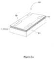
- FIG. 1 ais a pictorial view of a 3DS DRAM IC manufactured with Method A or Method B and demonstrating the same physical appearance of I/O bond pads as a conventional IC die;
- FIG. 1 bis a cross-sectional view of a 3DS memory IC showing the metal bonding interconnect between several thinned circuit layers;
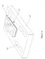
- FIG. 1 cis a pictorial view of a 3DS DRAM IC stack bonded and interconnected face-down onto a larger conventional IC or another 3DS IC;
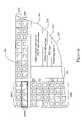
- FIG. 2 ais a diagram showing the physical layout of a 3DS DRAM array circuit block with one data-line set of bus lines, i.e. one port;
- FIG. 2 bis a diagram showing the physical layout of a 3DS DRAM array circuit block with two sets of data-line bus lines, i.e. two ports;
- FIG. 2 cis a diagram showing the physical layout of a portion of an exemplary memory controller circuit
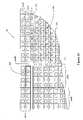
- FIG. 3is a diagram showing the physical layout of a 3DS DRAM array circuit showing partitions for sixty-four (64) 3DS DRAM array blocks;
- FIG. 4is a cross-sectional view of a generic 3DS vertical interconnection or feed-through in a thinned substrate
- FIG. 5is a diagram showing the layout of a 3DS memory multiplexer for down-selecting gate-line read or write selection.
- the 3DS (Threee Dimensional Structure) memory device 100is a stack of integrated circuit layers with fine-grain vertical interconnect between all circuit layers.
- the term fine-grain inter-layer vertical interconnectis used to mean electrical conductors that pass through a circuit layer with or without an intervening device element and have a pitch of nominally less than 100 ⁇ m and more typically less than 10 ⁇ m, but not limited to a pitch of less than 2 m, as best seen in FIG. 2 a and FIG. 2 b .
- the fine-grain inter-layer vertical interconnectalso functions to bond together the various circuit layers. As shown in FIG. 1 b , although the bond and interconnect layers 105 a , 105 b , etc., are preferably metal, other material may also be used as described more fully hereinafter.
- the pattern 107 a , 107 b , etc. in the bond and interconnect layers 105 a , 105 b , etc.defines the vertical interconnect contacts between the integrated circuit layers and serves to electrically isolate these contacts from each other and the remaining bond material; this pattern takes the form of either voids or dielectric filled spaces in the bond layers.
- the 3DS memory stackis typically organized as a controller circuit 101 and some number of memory array circuit layers 103 , typically between nine (9) and thirty-two (32), but there is no particular limit to the number of layers.
- the controller circuitis of nominal circuit thickness (typically 0.5 mm or greater), but each memory array circuit layer is a thinned and substantially flexible circuit with net low stress, less than 50 ⁇ m and typically less than 10 ⁇ m in thickness.
- Conventional I/O bond padsare formed on a final memory array circuit layer for use with conventional packaging methods.
- Other metal patternsmay be used such as insertion interconnection (disclosed in U.S. Pat. Nos. 5,323,035 and 5,453,404 of the present inventor), DCA (Direct Chip Attach) or FCA (Flip-Chip Attach) methods.
- the fine grain inter-layer vertical interconnectcan be used for direct singulated die bonding between a 3DS memory die and a conventional die (wherein the conventional die could be the controller circuit as shown in FIG. 1 c ) or a 3DS memory die and another 3DS memory die; it should be assumed that the areas (sizes) of the respective dice to be bonded together can vary and need not be the same.
- a 3DS DRAM IC stack 100is bonded and interconnected face-down onto a larger conventional IC or another 3DS IC 107 .
- the 3DS stack 100can be composed of only DRAM array circuits with the DRAM controller circuitry as part of the larger die.
- fine-grain vertical bus interconnectwould be required (at the face 109 of the 3DS DRAM IC stack 100 ) to connect the 3DS DRAM array circuit to the DRAM controller, otherwise larger grain conventional interconnection could be incorporated (patterned) into the planarized bond layer.
- each memory array circuit layerincludes a memory array circuit 300 composed of memory array blocks 301 (nominally less than 5 mm 2 in area) and each block is composed of memory cells (in much the same manner as the cell array of a DRAM or EEPROM circuit), busing electrodes, and—at the option of the designer—enabling gates for selection of specific rows or columns of the memory array.
- the controller circuitis composed of sense amps, address, control and drive logic that would normally be found at the periphery of a typical memory circuit of monolithic design such as in a conventional DRAM.
- Fine-grain busingvertically connects the controller independently to each memory array layer such that the controller can provide drive (power) or enable signals to any one layer without affecting the state of any of the other layers. This allows the controller to test, read or write independently each of the memory circuit layers.
- FIG. 2 a and FIG. 2 bshow examples of layouts of possible blocks of a memory array such as the block 301 of FIG. 3 . Although only a portion of the block is shown, in the illustrated embodiment, the blocks exhibit bilateral symmetry such that the layout of the complete block may be ascertained from the illustrated portion. Abbreviations “T”, “L”, and “TL” are used following various reference numerals to indicate “Top”, “Left” and “Top-Left,” respectively, implying corresponding elements not shown in the figure. Referring to FIG. 2 a , a core portion 200 of the block is composed of a “sea” of memory cells.
- the aggregation of memory cellsmay be subdivided into “macrocells” 201 each containing some number of memory cells, e.g. an 8 ⁇ 8 array of 64 memory cells.
- fine-grain vertical interconnectcomprising inter-layer bond and bus contact metallizations 400 , described in greater detail hereinafter with reference to FIG. 4 .
- the fine-grain vertical interconnectincludes I/O power and ground bus lines 203 TL, memory circuit layer selects 205 T, memory macro cell column selects 207 T, data lines 209 L, and gate-line multiplexer (“mux”) selects 209 TL.
- Gate-line multiplexers 211 Tare, in the illustrated embodiment, 4:1 multiplexers used to select one of four columns within an eight-wide memory macro cell column. Corresponding bottom-side 4:1 multiplexers combine with the topside multiplexers 211 T to form equivalent 8:1 multiplexers for selecting a single gate-line from an eight-gate-line-wide memory macro cell column.
- FIG. 5One implementation of a 4:1 gate-line bus muliplexer 500 is shown in FIG. 5 .
- Gate-line enables 209 TL′formed in a Metal-1 layer, for example
- control transistors 501 a through 501 drespectively. Coupled to the transistors are respective gate lines 503 a through 503 d .
- gate-lines 505 a through 505 dwhich are coupled to a corresponding 4:1 multiplexer (not shown).
- the corresponding gate-lineis coupled to an output line 507 of the multiplexer (formed in a Metal-2 layer, for example).
- the output lineis connected to one or more vertical bus connects through a line 509 (formed in a Metal-3 layer and corresponding to metal contact 400 of vertical bus interconnect, for example) and tungsten plugs 511 and 513 .
- the tungsten plug 513joins the line 509 to a vertical interconnect (not shown).
- the layermay also include output line enables (gates) from controller layer enable signals 205 T, for which I/O enables (gates) 213 may be provided.
- each memory block 301is electrically isolated from every other memory block 301 . Accordingly, the yield probability for each memory block is independent.
- Additional read/write portscan be added as can additional gate-line vertical interconnections; additional vertical interconnection can be used in a redundant manner to improve vertical interconnect yield.
- the 3DS memory circuitcan be designed to have one or more data read and write bus port interconnections. Referring to FIG. 2 b , a memory block 301 ′ is shown as having a port P 0 , ( 209 L) and a further port P 1 ( 209 L′).
- the only limitation on the number of vertical interconnectionsis the overhead such vertical interconnections impose on the cost of the circuit.
- the fine-grain vertical interconnect methodallows thousands of interconnects per block at an increase in die area of only a few percent.
- the overhead of the vertical interconnect shown in FIG. 2 b for a DRAM memory block of 4 bits with two read/write ports and implemented in 0.35 cm or 0.15 ⁇ m design rulesconsists of approximately 5,000 connections and is less than 6% of the total area of the memory array block. Therefore, the vertical interconnect overhead for each memory array circuit layer in the 3DS DRAM circuit is less than 6%. This is significantly less than that presently experienced in monolithic DRAM circuit designs where the percentage of non-memory cell area can exceed 40%. In a completed 3DS DRAM circuit the percentage of non-memory cell area is typically less than 10% of the total area of all circuits in the stacked structure.
- the 3DS memory devicedecouples control functions that normally would be found adjacent the memory cells of monolithic memory circuits and segregates them to the controller circuit.
- the control functionsrather than occurring on each memory array layer as in conventional memory ICs, occur only once in the controller circuit. This creates an economy by which several memory array layers share the same controller logic, and therefore, lowers the net cost per memory cell by as much as a factor of two versus conventional memory design.
- control functionsto a separate controller circuit allows more area for such functions (i.e., an area equal to the area one or several of the memory array blocks).
- This physical segregation by functionalso allows fabrication process segregation of the two very different fabrication technologies used for the control logic and the memory array, again realizing additional fabrication cost savings versus the more complicated combined logic/memory fabrication process used for conventional memory.
- the memory arraycan also be fabricated in a process technology without consideration of the process requirements of control logic functions. This results in the ability to design higher performance controller functions at lower cost than is the case with present memory circuits.
- the memory array circuitcan also be fabricated with fewer process steps and nominally reduce memory circuit fabrication costs by 30% to 40% (e.g., in the case of a DRAM array, the process technology can be limited to NMOS or PMOS transistors versus CMOS).
- the inventioncontemplates bonding of separate memory controller and memory array substrates by any of various conventional surface bonding methods, such as anisotropically conductive epoxy adhesive, to form interconnects between the two to provide random access data storage.
- FIG. 2 cthe layout of a portion of an exemplary memory controller circuit is shown.
- the inter-layer bond and bus contact metallizationhas the same pattern as previously described in relation to FIG. 2 a .
- memory controller circuitryincluding, for example, sense amps and data line buffers 215 .
- sense amps and data line buffers 215are also shown.
- multi-level logicmay be provided in conjunction with the sense amps and data line buffers 215 .
- self-test logicECC logic, and windowing logic are provided in addition to functions normally found within a DRAM memory controller circuit.
- any of numerous other functionsmay also be provided including, for example, virtual memory management, address functions such as indirect addressing or content addressing, data compression, data decompression, audio encoding, audio decoding, video encoding, video decoding, voice recognition, handwriting recognition, power management, database processing, graphics acceleration functions, microprocessor functions (including adding a microprocessor substrate), etc.
- the size of the 3DS memory circuit dieis not dependent on the present constraint of containing the necessary number of memory cells and control function logic on one monolithic layer. This allows the circuit designer to reduce the 3DS circuit die size or choose a die size that is more optimal for the yield of the circuit.
- 3DS memory circuit die sizeis primarily a function of the size and number of memory array blocks and the number of memory array layers used to fabricate the final 3DS memory circuit. (The yield of a nineteen (19) layer, 0.25 ⁇ m process 3DS DRAM memory circuit may be shown to be greater than 90% as described below.)
- This advantage of selecting the 3DS circuit die sizeenables an earlier first production use of a more advanced process technology than would normally be possible for conventional monolithic circuit designs. This, of course, implies additional cost reductions and greater performance over the conventional memory circuits.
- the two 3DS memory fabrication methodshave a common objective which is the thermal diffusion metal bonding (also referred to as thermal compression bonding) of a number of circuit substrates onto a rigid supporting or common substrate which itself may optionally also be a circuit component layer.
- the supporting or common substratecan be a standard semiconductor wafer, a quartz wafer or a substrate of any material composition that is compatible with the processing steps of the 3DS circuit, the operation of the circuit and the processing equipment used.
- the size and shape of the supporting substrateis a choice that best optimizes available manufacturing equipment and methods.
- Circuit substratesare bonded to the supporting substrate and then thinned through various methods.
- Circuit substratesmay be formed on standard single crystal semiconductor substrates or as polysilicon circuits formed on an appropriate substrate such as silicon or quartz.
- Polysilicon transistor circuitshave the important cost saving option of incorporating a parting layer (film) that allows the substrate upon which the polysilicon circuits are formed to be released and reused.
- Polysilicon transistor or TFTs (Thin Film Transistor) devicesare widely used, and need not be made solely from silicon.
- the various circuit layers of the 3DS memory circuitare bonded together by use of thermal diffusion of two metal surfaces, typically aluminum.
- the surface of the circuits to be bondedare smooth and sufficiently planar as is the case with the surface of an unprocessed semiconductor wafer or a processed semiconductor wafer that has been planarized with the CMP (Chemical Mechanical Processing) method with a surface planarity of less than 1 ⁇ m and preferably less than 1,000 ⁇ over at least the area of the surface of the circuit (formed on the substrate) to be bonded.
- the metal bonding material on the surfaces of the circuits to be bondedare patterned to be mirror images of each other and to define the various vertical interconnect contacts as indicated in FIG. 2 a , FIG. 2 b , FIG. 2 c and FIG. 5 .
- the step of bonding two circuit substratesresults in simultaneously forming the vertical interconnection between the two respective circuit layers or substrates.
- the thermal diffusion bonding of the circuit layerstakes place preferably in an equipment chamber with controlled pressure and atmospheric components such as N 2 with little H 2 O and O 2 content.
- the bonding equipmentaligns the patterns of the substrates to be bonded, presses them together with a set of programmed pressures and at one or more temperatures for a period of time as required by the type of metal used as the bonding material.
- the thickness of the bonding materialis nominally in a range of 500 ⁇ to 15,000 ⁇ or greater with a preferred thickness of 1,500 ⁇ .
- the initial bonding of the substratesis preferably done at lower than standard pressure such as a negative pressure between 1 torr and 740 torr depending on the design of the bond pattern. This can leave an interior negative pressure between the bonding surfaces once external atmospheric pressure is returned which further assists in the formation of the bond and enhances the reliability of the bond.
- the preferred bonding materialis pure aluminum or an alloy of aluminum, but it is not limited to aluminum and may include, for example, such metals as Sn, Ti, In, Pb, Zn, Ni, Cu, Pt, Au or alloys of such metals that provide acceptable surface bond diffusion capabilities at acceptable temperatures and forming periods.
- the bonding materialis not limited to metal, and could be a combination of bonding materials, such as highly conductive polysilicon, some of which are non-conducting such as silicon dioxide, and the foregoing exemplary types of bond material choices should not be considered to be limitations on how the circuit layers can be bonded.
- the oxideshould be removed.
- the bonding equipmentprovides an oxide reduction capability such that bonding surfaces of the bond material are rendered without native surface oxide.
- the methods of forming gas atmospheres for the reduction of surface oxidesare well known, and there arc other methods for removing the native oxide such as sputter etching, plasma etching or ion mill etching.
- the thin native aluminum oxide film of approximately 40 ⁇ on the bonding surfacesbe removed prior to bonding.
- the thinned (substantially flexible) substrate circuit layers of the 3DS memory circuitare typically memory array circuits, however, the thinned substrate circuit layers are not limited to memory circuits.
- Other circuit layer typescan be controller circuits, non-volatile memory such as EEPROM, additional logic circuitry including microprocessor logic and application specific logic functions such as those that support graphic or database processing, etc. The selection of such circuit layer types follows from the functional requirements of the design of the circuit and is not limited by the 3DS memory fabrication process.
- the thinned (substantially flexible) substrate circuit layersare preferably made with dielectrics in low stress (less than 5 ⁇ 10 8 dynes/cm 2 ) such as low stress silicon dioxide and silicon nitride dielectrics as opposed to the more commonly used higher stress dielectrics of silicon oxide and silicon nitride used in conventional memory circuit fabrication.
- low stress dielectricsare discussed at length in U.S. Pat. No. 5,354,695 of the present inventor, incorporated herein by reference.
- each layer in the assemblywill have to be stress balanced so that the net stress of the deposited films of a layer is less than 5 ⁇ 10 8 dynes/cm 2 .
- the use of intrinsically low stress deposited filmsis the preferred method of fabrication versus the use of the method where the stress of individually deposited films are not equal but are deposited to create a net balanced lower stress.
- FIG. 1 aAn example of a resulting 3DS memory circuit is shown in FIG. 1 a.
- an etch stopmay be incorporated in the second substrate from less than a micron to several microns below the semiconductor surface prior to device fabrication.
- This etch stopcan be an epitaxially formed film such as GeB (described in U.S. Pat. Nos. 5,354,695 and 5,323,035 of the present inventor, incorporated herein by reference) or a low density implanted layer of O 2 or N 2 to form a buried oxide or nitride barrier etch stop layer just below the device layer on the topside of the second substrate.
- the remaining portion of the backside of the second substrateis then selectively etched in a chemical bath which stops on the surface of the eptiaxial or implanted layer. Subsequent polishing and RIE steps as necessary can then be used to complete the thinning of the second substrate.
- a parting layer such as H 2 implanted into the topside surface of the second substrate prior to device fabricationcan be used with a thermal step to crack off the majority of the backside of the second substrate, allowing its reuse.
- the second substratemay alternatively be a circuit formed of polysilicon transistors or TFTs over a parting layer such as aluminum, titanium, A1As, KBr, etc. which can be activated by a specific chemical release agent.
- the backside of the second substrateis then removed upon activating (dissolving) the release layer and followed as needed by interconnect semiconductor processing steps.
- the backside processingtypically comprises conventional semiconductor processing steps of dielectric and metal deposition, lithography and RIE, the order of which can vary to a great degree.
- a patterned metal layerthat is similar to the topside bond material pattern to facilitate the subsequent bonding of an additional circuit substrate, a terminal pattern such as a conventional I/O IC bond pad (wire bonding) pattern, a pattern for thermal diffusion bonding of the 3DS memory circuit to another die (either another 3DS circuit or a conventional die), or a pattern for insertion interconnection, conventional DCA (Direct Chip Attach) or FCA (Flip-Chip Attach).
- a terminal patternsuch as a conventional I/O IC bond pad (wire bonding) pattern, a pattern for thermal diffusion bonding of the 3DS memory circuit to another die (either another 3DS circuit or a conventional die), or a pattern for insertion interconnection, conventional DCA (Direct Chip Attach) or FCA (Flip-Chip Attach).
- an oxide mask 401is thermally grown or deposited.
- Vertical bus contacts 403are then formed, for example from highly-doped polysilicon coincident with a polysilicon gate forming step. Alternatively, contact 403 may be formed of metal.
- Conventional DRAM interconnect structures 410are then formed using conventional processing.
- the DRAM interconnectmay include an internal pad 405 .
- the “DRAM processed” portion 420 of the waferincludes various dielectric and metal layers.
- a final passivation layer 407is deposited, after which vias 409 are formed. Conventional CMP processing is then used to obtain a planar surface 411 . Contacts 413 and bond surfaces not shown are then patterned in a top-most metal layer (e.g, Metal-3).
- feed-throughs 417are then formed in registration with the contacts 403 .
- a passivation layer 419 and contacts 421are then formed.
- the contacts 421may be formed so as to form a mirror image of the contacts 413 , allowing for the bonding of further wafers.
- steps 1-3are repeated.
- circuits of the finished 3DS memory substrateare then conventionally sawed into die (singulated), resulting in a circuit of the type shown in FIG. 1 a , and packaged as would be the case with conventional integrated circuits.
- the circuits of the finished 3DS memory substrateare then conventionally sawed and then individually aligned and thermal diffusion bonded (metal pattern down) to the surface of a second (conventional IC) die or MCM substrate in a manner similar to that used in the bonding of the circuit substrates of step 1 above.
- the conventional die or MCM substratemay have a larger area than the 3DS memory substrate and may include a graphics controller, video controller or microprocessor, such that the 3DS becomes embedded as part of another circuit.
- This final bonding steptypically incorporates a fine-grain interconnect between the 3DS memory circuit and the die or MCM substrate, but could also use a conventional interconnect pattern.
- a 3DS memory circuitcan be bonded face up to a conventional IC in die form or MCM substrate and wire bonding used to form conventional I/O interconnections.
- This fabrication sequenceassumes that a circuit substrate will first be bonded to a transfer substrate, thinned and then bonded to a common substrate as a layer of the circuit stack. The transfer substrate is then released.
- This methodhas the advantage over Method A of allowing substrates to be thinned prior to being bonded to the final circuit stack and allows for simultaneous thinning and vertical interconnect processing of substrate circuit layers.
- a transfer substratemay have high tolerance parallel surfaces (TTV or Total Thickness Variance of less than 1 ⁇ m) and may be perforated with an array of small holes to assist the parting process.
- the parting layercan be a blanket deposition of a bonding metal. Precise alignment of the surfaces is not required.
- the backside processingtypically comprises conventional semiconductor processing steps of dielectric and metal deposition, lithography and RIE, the order of which can vary to great degree.
- the completion of the backside processingwill also result in a patterned metal layer that is similar to the bond material pattern of the common substrate to facilitate the subsequent bonding of an additional circuit layer.
- the 3DS circuitmay be considered a vertically assembled MCM (Multi-Chip Module) and as with an MCM the final yield is the product of the yield probabilities of each component circuit (layer) in the completed 3DS circuit.
- the 3DS circuituses several yield enhancement methods that are synergistic in their combined usage within a single memory IC.
- the yield enhancement methods used in the 3DS memory circuitinclude small memory array block size, memory array block electrical isolation through physically unique or separate vertical bus interconnections, intra memory array block gate-line sparing, memory array layer sparing (inter-block gate-line sparing), controller sparing and ECC (Error Correcting Codes).
- sparingis used to mean substitution by a redundant element.
- the selected size of the memory array blockis the first component in the yield equation for the 3DS memory circuit.
- Each memory array blockis individually (uniquely) accessed and powered by the controller circuit and is physically independent of each and every other memory array block including those on the same memory array layer in addition to those on a different memory array layer.
- the size of the memory array blockis typically less than 5 mm 2 and preferably less than 3 mm 2 , but is not limited to a specific size.
- the size of memory array block, the simplicity of its NMOS or PMOS fabrication process and its physical independence from each of the other memory array blocks, for nearly all production IC processes,provides a conservatively stated nominal yield of greater than 99.5%.
- the stack yield Ys for the complete memory arrayis 97.47%.
- the Ys memory array stack yieldis then multiplied by the yield of the controller Yc. Assuming a die size of less than 50 mm 2 , a reasonable Yc for a controller fabricated from a 0.5 cm BiCMOS or mixed signal process would be between 65% and 85%, giving a net 3DS memory circuit yield of between 63.4% and 82.8%. If a redundant controller circuit layer is added to the 3DS memory stack, the yield probabilities would be between 85.7% and 95.2%.
- ECC logiccorrects data bit errors for some group size of data bits.
- the syndrome bits necessary for the operation of ECC logicwould be stored on redundant gate-lines of any of the memory array layers in a vertically associated block stack. Further, if necessary, in order to accommodate the storage of ECC syndrome bits, additional memory array layers could be added to the circuit.
- the 3DS memory controller circuitcan have various advantageous capabilities due the additional area available for controller circuitry and the availability of various mixed signal process fabrication technologies. Some of these capabilities are self-test of memory cells with dynamic gate-line address assignment, virtual address translation, programmable address windowing or mapping, ECC, data compression and multi-level storage.
- Dynamic gate-line address assignmentis the use of programmable gates to enable the layer and gate-line for a read/write operation. This allows the physical order of memory storage to be separate or different from the logical order of stored memory.
- the testing of each generation of memory deviceshas resulted in significantly increased test costs.
- the 3DS memory controllerreduces the cost of testing by incorporating sufficient control logic to perform an internal test (self-test) of the various memory array blocks. Circuit testing in the conventional ATE manner is required only for verification of controller circuit functions. The scope of the internal test is further extended to the programmable (dynamic) assignment of unique addresses corresponding to the various gate-lines of each memory array block on each layer. Self-test capability of the 3DS controller circuit can be used anytime during the life of the 3DS memory circuit as a diagnostic tool and as a means to increase circuit reliability by reconfiguring (sparing) the addresses of gate-lines that fail after the 3DS memory circuit is in use in a product.
- ECCis a circuit capability that, if included in the controller circuit, can be enabled or disabled by a programming signal or made a dedicated function.
- Data compression logicwill allow the total amount of data that can be stored in the 3DS memory array to be increased. There are various generally known data compression methods available for this purpose.
Landscapes
- Engineering & Computer Science (AREA)
- Power Engineering (AREA)
- Microelectronics & Electronic Packaging (AREA)
- General Physics & Mathematics (AREA)
- Condensed Matter Physics & Semiconductors (AREA)
- Computer Hardware Design (AREA)
- Physics & Mathematics (AREA)
- Semiconductor Memories (AREA)
- Dram (AREA)
- Semiconductor Integrated Circuits (AREA)
- Manufacturing & Machinery (AREA)
- Internal Circuitry In Semiconductor Integrated Circuit Devices (AREA)
- Design And Manufacture Of Integrated Circuits (AREA)
Abstract
Description
- 1. Field of the Invention
- The present invention relates to stacked integrated circuit memory.
- 2. State of the Art
- Manufacturing methods for increasing the performance and decreasing the cost of electronic circuits, nearly without exception, are methods that increase the integration of the circuit and decrease its physical size per equivalent number of circuit devices such as transistors or capacitors. These methods have produced as of 1996 microprocessors capable of over 100 million operations per second that cost less than $1,000 and 64 Mbit DRAM circuits that access data in less than 50 ns and cost less than $50. The physical size of such circuits is less than 2 cm.Such manufacturing methods support to a large degree the economic standard of living in the major industrialized countries and will most certainly continue to have significant consequences in the daily lives of people all over the world.
- Circuit manufacturing methods take two primary forms: process integration and assembly integration. Historically the line between these two manufacturing disciplines has been clear, but recently with the rise in the use of MCMs (Multi-Chip Modules) and flip-chip die attach, this clear separation may soon disappear. (The predominate use of the term Integrated Circuit (IC) herein is in reference to an Integrated Circuit in singulated die form as sawed from a circuit substrate such as s semiconductor wafer versus, for example, an Integrated Circuit in packaged form.) The majority of ICs when in initial die form are presently individually packaged, however, there is an increasing use of MCMs. Die in an MCM are normally attached to a circuit substrate in a planar fashion with conventional IC die I/O interconnect bonding methods such as wire bonding, DCA (Direct Chip Attach) or FCA (Flip-Chip Attach).
- Integrated circuit memory such as DRAM, SRAM, flash EPROM, EEPROM, Ferroelectric, GMR (Giant MagnetoResistance), etc. have the common architectural or structural characteristic of being monolithic with the control circuitry integrated on the same die with the memory array circuitry. This established (standard or conventional) architecture or circuit layout structure creates a design trade-off constraint between control circuitry and memory array circuitry for large memory circuits. Reductions in the fabrication geometries of memory cell circuitry has resulted in denser and denser memory ICs, however, these higher memory densities have resulted in more sophisticated control circuitry at the expense of increased area of the IC. Increased IC area means at least higher fabrication costs per IC (fewer ICs per wafer) and lower IC yields (fewer working ICs per wafer), and in the worst case, an IC design that cannot be manufactured due to its non-competitive cost or unreliable operation.
- As memory density increases and the individual memory cell size decreases more control circuitry is required. The control circuitry of a memory IC as a percentage of IC area in some cases such as DRAMs approaches or exceeds 40%. One portion of the control circuitry is the sense amp which senses the state, potential or charge of a memory cell in the memory array circuitry during a read operation. The sense amp circuitry is a significant portion of the control circuitry and it is a constant challenge to the IC memory designer to improve sense amp sensitivity in order to sense ever smaller memory cells while preventing the area used by the sense amp from becoming too large.
- If this design constraint or trade-off between control and memory circuits did not exist, the control circuitry could be made to perform numerous additional functions, such as sensing multiple storage states per memory cell, faster memory access through larger more sensitive sense amps, caching, refresh, address translation, etc. But this trade-off is the physical and economic reality for memory ICs as they are presently made by all manufacturers.
- The capacity of DRAM circuits increases by a factor of four from one generation to the next; e.g. 1 bit, 4 bit, 16 Mbit and 64 Mbit DRAMs. This four times increase in circuit memory capacity per generation has resulted in larger and larger DRAM circuit areas. Upon introduction of a new DRAM generation the circuit yields are too low and, therefore, not cost effective for high volume manufacture. It is normally several years between the date prototype samples of a new DRAM generation are shown and the date such circuits are in volume production.
- Assembling die in a stacked or three dimensional (3D) manner is disclosed in U.S. Pat. No. 5,354,695 of the present inventor, incorporated herein by reference. Furthermore, assembling die in a 3D manner has been attempted with regard to memory. Texas Instruments of Dallas Tex., Irvine Sensors of Costa Mesa Calif. and Cubic Memory Corporation of Scotts Valley Calif. have all attempted to produce stacked or 3D DRAM products. In all three cases, conventional DRAM circuits in die form were stacked and the interconnect between each DRAM in the stack was formed along the outside surface of the circuit stack. These products have been available for the past several years and have proved to be too expensive for commercial applications, but have found some use in space and military applications due to their small physical size or footprint.
- The DRAM circuit type is referred to and often used as an example in this specification, however, this invention is clearly not limited to the DRAM type of circuit. Undoubtedly memory cell types such as EEPROMs (Electrically Erasable Programmable Read Only Memories), flash EPROM, Ferroelectric, GMR Giant Magneto Resistance or combinations (intra or inter) of such memory cells can also be used with the present Three Dimensional Structure (3DS) methods to form 3DS memory devices.
- The present invention furthers, among others, the following objectives:
- 1. Several-fold lower fabrication cost per megabyte of memory than circuits conventionally made solely with monolithic circuit integration methods.
2. Several-fold higher performance than conventionally made memory circuits.
3. Many-fold higher memory density per IC than conventionally made memory circuits.
4. Greater designer control of circuit area size, and therefore, cost.
5. Circuit dynamic and static self-test of memory cells by an internal controller.
6. Dynamic error recovery and reconfiguration.
7. Multi-level storage per memory cell.
8. Virtual address translation, address windowing, various address functions such as indirect addressing or content addressing, analog circuit functions and various graphics acceleration and microprocessor functions. - The present 3DS memory technology is a stacked or 3D circuit assembly technology. Features include:
- 1. Physical separation of the memory circuits and the control logic circuit onto different layers;
2. The use of one control logic circuit for several memory circuits;
3. Thinning of the memory circuit to less than about 50 μm in thickness forming a substantially flexible substrate with planar processed bond surfaces and bonding the circuit to the circuit stack while still in wafer substrate form; and
4. The use of fine-grain high density inter layer vertical bus connections. - The 3DS memory manufacturing method enables several performance and physical size efficiencies, and is implemented with established semiconductor processing techniques. Using the DRAM circuit as an example, a 64 Mbit DRAM made with a 0.25 μm process could have a die size of 84 mm2, a memory area to die size ratio of 40% and a access time of about 50 ns for 8 Mbytes of storage; a 3DS DRAM IC made with the same 0.25 μm process would have a die size of 18.6 mm2, use 17 DRAM array circuit layers, a memory area to die size ratio of 94.4% and an expected access time of less than 10 ns for 64 Mbytes of storage. The 3DS DRAM IC manufacturing method represents a scalable, many-fold reduction in the cost per megabyte versus that of conventional DRAM IC manufacturing methods. In other words, the 3DS memory manufacturing method represents, at the infrastructure level, a fundamental cost savings that is independent of the process fabrication technology used.
- The present invention may be further understood from the following description in conjunction with the appended drawing. In the drawing:
FIG. 1 ais a pictorial view of a 3DS DRAM IC manufactured with Method A or Method B and demonstrating the same physical appearance of I/O bond pads as a conventional IC die;FIG. 1 bis a cross-sectional view of a 3DS memory IC showing the metal bonding interconnect between several thinned circuit layers;FIG. 1 cis a pictorial view of a 3DS DRAM IC stack bonded and interconnected face-down onto a larger conventional IC or another 3DS IC;FIG. 2 ais a diagram showing the physical layout of a 3DS DRAM array circuit block with one data-line set of bus lines, i.e. one port;FIG. 2 bis a diagram showing the physical layout of a 3DS DRAM array circuit block with two sets of data-line bus lines, i.e. two ports;FIG. 2 cis a diagram showing the physical layout of a portion of an exemplary memory controller circuit;FIG. 3 is a diagram showing the physical layout of a 3DS DRAM array circuit showing partitions for sixty-four (64) 3DS DRAM array blocks;FIG. 4 is a cross-sectional view of a generic 3DS vertical interconnection or feed-through in a thinned substrate;FIG. 5 is a diagram showing the layout of a 3DS memory multiplexer for down-selecting gate-line read or write selection.- Referring to
FIG. 1 aandFIG. 1 b, the 3DS (Three Dimensional Structure)memory device 100 is a stack of integrated circuit layers with fine-grain vertical interconnect between all circuit layers. The term fine-grain inter-layer vertical interconnect is used to mean electrical conductors that pass through a circuit layer with or without an intervening device element and have a pitch of nominally less than 100 μm and more typically less than 10 μm, but not limited to a pitch of less than 2 m, as best seen inFIG. 2 aandFIG. 2 b. The fine-grain inter-layer vertical interconnect also functions to bond together the various circuit layers. As shown inFIG. 1 b, although the bond andinterconnect layers - The
pattern interconnect layers - The 3DS memory stack is typically organized as a
controller circuit 101 and some number of memory array circuit layers103, typically between nine (9) and thirty-two (32), but there is no particular limit to the number of layers. The controller circuit is of nominal circuit thickness (typically 0.5 mm or greater), but each memory array circuit layer is a thinned and substantially flexible circuit with net low stress, less than 50 μm and typically less than 10 μm in thickness. Conventional I/O bond pads are formed on a final memory array circuit layer for use with conventional packaging methods. Other metal patterns may be used such as insertion interconnection (disclosed in U.S. Pat. Nos. 5,323,035 and 5,453,404 of the present inventor), DCA (Direct Chip Attach) or FCA (Flip-Chip Attach) methods. - Further, the fine grain inter-layer vertical interconnect can be used for direct singulated die bonding between a 3DS memory die and a conventional die (wherein the conventional die could be the controller circuit as shown in
FIG. 1 c) or a 3DS memory die and another 3DS memory die; it should be assumed that the areas (sizes) of the respective dice to be bonded together can vary and need not be the same. Referring more particularly toFIG. 1 c, a 3DSDRAM IC stack 100 is bonded and interconnected face-down onto a larger conventional IC or another3DS IC 107. Optionally the3DS stack 100 can be composed of only DRAM array circuits with the DRAM controller circuitry as part of the larger die. If the DRAM controller circuitry is part of the larger die, then fine-grain vertical bus interconnect would be required (at theface 109 of the 3DS DRAM IC stack100) to connect the 3DS DRAM array circuit to the DRAM controller, otherwise larger grain conventional interconnection could be incorporated (patterned) into the planarized bond layer. - As shown in
FIG. 3 , each memory array circuit layer includes amemory array circuit 300 composed of memory array blocks301 (nominally less than 5 mm2in area) and each block is composed of memory cells (in much the same manner as the cell array of a DRAM or EEPROM circuit), busing electrodes, and—at the option of the designer—enabling gates for selection of specific rows or columns of the memory array. The controller circuit is composed of sense amps, address, control and drive logic that would normally be found at the periphery of a typical memory circuit of monolithic design such as in a conventional DRAM. - Fine-grain busing vertically connects the controller independently to each memory array layer such that the controller can provide drive (power) or enable signals to any one layer without affecting the state of any of the other layers. This allows the controller to test, read or write independently each of the memory circuit layers.
FIG. 2 aandFIG. 2 bshow examples of layouts of possible blocks of a memory array such as theblock 301 ofFIG. 3 . Although only a portion of the block is shown, in the illustrated embodiment, the blocks exhibit bilateral symmetry such that the layout of the complete block may be ascertained from the illustrated portion. Abbreviations “T”, “L”, and “TL” are used following various reference numerals to indicate “Top”, “Left” and “Top-Left,” respectively, implying corresponding elements not shown in the figure. Referring toFIG. 2 a, acore portion 200 of the block is composed of a “sea” of memory cells. Logically, the aggregation of memory cells may be subdivided into “macrocells”201 each containing some number of memory cells, e.g. an 8×8 array of 64 memory cells. At the periphery of the core is formed fine-grain vertical interconnect comprising inter-layer bond andbus contact metallizations 400, described in greater detail hereinafter with reference toFIG. 4 . The fine-grain vertical interconnect includes I/O power and ground bus lines203TL, memory circuit layer selects205T, memory macro cell column selects207T, data lines209L, and gate-line multiplexer (“mux”) selects209TL. Gate-line multiplexers 211T are, in the illustrated embodiment, 4:1 multiplexers used to select one of four columns within an eight-wide memory macro cell column. Corresponding bottom-side 4:1 multiplexers combine with thetopside multiplexers 211T to form equivalent 8:1 multiplexers for selecting a single gate-line from an eight-gate-line-wide memory macro cell column.- One implementation of a 4:1 gate-
line bus muliplexer 500 is shown inFIG. 5 . Gate-line enables209TL′ (formed in a Metal-1 layer, for example)control transistors 501athrough501d, respectively. Coupled to the transistors arerespective gate lines 503athrough503d. Also partly visible are gate-lines 505athrough505dwhich are coupled to a corresponding 4:1 multiplexer (not shown). When one of the gate-line enables is active, the corresponding gate-line is coupled to anoutput line 507 of the multiplexer (formed in a Metal-2 layer, for example). The output line is connected to one or more vertical bus connects through a line509 (formed in a Metal-3 layer and corresponding tometal contact 400 of vertical bus interconnect, for example) and tungsten plugs511 and513. Thetungsten plug 513 joins theline 509 to a vertical interconnect (not shown). - Referring again to
FIG. 2 a, in the case of a memory circuit layer, the layer may also include output line enables (gates) from controller layer enablesignals 205T, for which I/O enables (gates)213 may be provided. - Note that at the memory layer level, each
memory block 301 is electrically isolated from everyother memory block 301. Accordingly, the yield probability for each memory block is independent. - Additional read/write ports can be added as can additional gate-line vertical interconnections; additional vertical interconnection can be used in a redundant manner to improve vertical interconnect yield. The 3DS memory circuit can be designed to have one or more data read and write bus port interconnections. Referring to
FIG. 2 b, amemory block 301′ is shown as having a port P0, (209L) and a further port P1(209L′). The only limitation on the number of vertical interconnections is the overhead such vertical interconnections impose on the cost of the circuit. The fine-grain vertical interconnect method allows thousands of interconnects per block at an increase in die area of only a few percent. - As an example, the overhead of the vertical interconnect shown in
FIG. 2 bfor a DRAM memory block of 4 bits with two read/write ports and implemented in 0.35 cm or 0.15 μm design rules consists of approximately 5,000 connections and is less than 6% of the total area of the memory array block. Therefore, the vertical interconnect overhead for each memory array circuit layer in the 3DS DRAM circuit is less than 6%. This is significantly less than that presently experienced in monolithic DRAM circuit designs where the percentage of non-memory cell area can exceed 40%. In a completed 3DS DRAM circuit the percentage of non-memory cell area is typically less than 10% of the total area of all circuits in the stacked structure. - The 3DS memory device decouples control functions that normally would be found adjacent the memory cells of monolithic memory circuits and segregates them to the controller circuit. The control functions, rather than occurring on each memory array layer as in conventional memory ICs, occur only once in the controller circuit. This creates an economy by which several memory array layers share the same controller logic, and therefore, lowers the net cost per memory cell by as much as a factor of two versus conventional memory design.
- The segregation of the control functions to a separate controller circuit allows more area for such functions (i.e., an area equal to the area one or several of the memory array blocks). This physical segregation by function also allows fabrication process segregation of the two very different fabrication technologies used for the control logic and the memory array, again realizing additional fabrication cost savings versus the more complicated combined logic/memory fabrication process used for conventional memory. The memory array can also be fabricated in a process technology without consideration of the process requirements of control logic functions. This results in the ability to design higher performance controller functions at lower cost than is the case with present memory circuits. Furthermore, the memory array circuit can also be fabricated with fewer process steps and nominally reduce memory circuit fabrication costs by 30% to 40% (e.g., in the case of a DRAM array, the process technology can be limited to NMOS or PMOS transistors versus CMOS).
- Hence, although bonding of sufficiently planar surfaces of a memory controller substrate and a memory array substrate using thermal diffusion metal bonding is preferred, in the broader aspects of the present invention, the invention contemplates bonding of separate memory controller and memory array substrates by any of various conventional surface bonding methods, such as anisotropically conductive epoxy adhesive, to form interconnects between the two to provide random access data storage.
- Referring to
FIG. 2 c, the layout of a portion of an exemplary memory controller circuit is shown. The inter-layer bond and bus contact metallization has the same pattern as previously described in relation toFIG. 2 a. Instead of a sea of memory cells, however, there is provided memory controller circuitry including, for example, sense amps and data line buffers215. Because of the increased availability of die area, multi-level logic may be provided in conjunction with the sense amps and data line buffers215. Also shown are address decode, gate-line and DRAM layerselect logic 217, refresh and self-test logic 219,ECC logic 221,windowing logic 223, etc. Note that self-test logic, ECC logic, and windowing logic are provided in addition to functions normally found within a DRAM memory controller circuit. Depending on die size or the number of controller circuit layers used, any of numerous other functions may also be provided including, for example, virtual memory management, address functions such as indirect addressing or content addressing, data compression, data decompression, audio encoding, audio decoding, video encoding, video decoding, voice recognition, handwriting recognition, power management, database processing, graphics acceleration functions, microprocessor functions (including adding a microprocessor substrate), etc. - The size of the 3DS memory circuit die is not dependent on the present constraint of containing the necessary number of memory cells and control function logic on one monolithic layer. This allows the circuit designer to reduce the 3DS circuit die size or choose a die size that is more optimal for the yield of the circuit. 3DS memory circuit die size is primarily a function of the size and number of memory array blocks and the number of memory array layers used to fabricate the final 3DS memory circuit. (The yield of a nineteen (19) layer, 0.25 μm process 3DS DRAM memory circuit may be shown to be greater than 90% as described below.) This advantage of selecting the 3DS circuit die size enables an earlier first production use of a more advanced process technology than would normally be possible for conventional monolithic circuit designs. This, of course, implies additional cost reductions and greater performance over the conventional memory circuits.
- There are two principal fabrication methods for 3DS memory circuits. The two 3DS memory fabrication methods, however, have a common objective which is the thermal diffusion metal bonding (also referred to as thermal compression bonding) of a number of circuit substrates onto a rigid supporting or common substrate which itself may optionally also be a circuit component layer.
- The supporting or common substrate can be a standard semiconductor wafer, a quartz wafer or a substrate of any material composition that is compatible with the processing steps of the 3DS circuit, the operation of the circuit and the processing equipment used. The size and shape of the supporting substrate is a choice that best optimizes available manufacturing equipment and methods. Circuit substrates are bonded to the supporting substrate and then thinned through various methods. Circuit substrates may be formed on standard single crystal semiconductor substrates or as polysilicon circuits formed on an appropriate substrate such as silicon or quartz. Polysilicon transistor circuits have the important cost saving option of incorporating a parting layer (film) that allows the substrate upon which the polysilicon circuits are formed to be released and reused. Polysilicon transistor or TFTs (Thin Film Transistor) devices are widely used, and need not be made solely from silicon.
- The various circuit layers of the 3DS memory circuit are bonded together by use of thermal diffusion of two metal surfaces, typically aluminum. The surface of the circuits to be bonded are smooth and sufficiently planar as is the case with the surface of an unprocessed semiconductor wafer or a processed semiconductor wafer that has been planarized with the CMP (Chemical Mechanical Processing) method with a surface planarity of less than 1 μm and preferably less than 1,000 Å over at least the area of the surface of the circuit (formed on the substrate) to be bonded. The metal bonding material on the surfaces of the circuits to be bonded are patterned to be mirror images of each other and to define the various vertical interconnect contacts as indicated in
FIG. 2 a,FIG. 2 b,FIG. 2 candFIG. 5 . The step of bonding two circuit substrates results in simultaneously forming the vertical interconnection between the two respective circuit layers or substrates. - The thermal diffusion bonding of the circuit layers takes place preferably in an equipment chamber with controlled pressure and atmospheric components such as N2with little H2O and O2content. The bonding equipment aligns the patterns of the substrates to be bonded, presses them together with a set of programmed pressures and at one or more temperatures for a period of time as required by the type of metal used as the bonding material. The thickness of the bonding material is nominally in a range of 500 Å to 15,000 Å or greater with a preferred thickness of 1,500 Å. The initial bonding of the substrates is preferably done at lower than standard pressure such as a negative pressure between 1 torr and 740 torr depending on the design of the bond pattern. This can leave an interior negative pressure between the bonding surfaces once external atmospheric pressure is returned which further assists in the formation of the bond and enhances the reliability of the bond.
- The preferred bonding material is pure aluminum or an alloy of aluminum, but it is not limited to aluminum and may include, for example, such metals as Sn, Ti, In, Pb, Zn, Ni, Cu, Pt, Au or alloys of such metals that provide acceptable surface bond diffusion capabilities at acceptable temperatures and forming periods. The bonding material is not limited to metal, and could be a combination of bonding materials, such as highly conductive polysilicon, some of which are non-conducting such as silicon dioxide, and the foregoing exemplary types of bond material choices should not be considered to be limitations on how the circuit layers can be bonded.
- In the case where metal bond materials form a native surface oxide that either inhibits the forming of a satisfactory bond or may increase the resistance in the vertical interconnections formed by the bond, the oxide should be removed. The bonding equipment provides an oxide reduction capability such that bonding surfaces of the bond material are rendered without native surface oxide. The methods of forming gas atmospheres for the reduction of surface oxides are well known, and there arc other methods for removing the native oxide such as sputter etching, plasma etching or ion mill etching. In the case where aluminum is used as the bonding material, it is preferred that the thin native aluminum oxide film of approximately 40 Å on the bonding surfaces be removed prior to bonding.
- The thinned (substantially flexible) substrate circuit layers of the 3DS memory circuit are typically memory array circuits, however, the thinned substrate circuit layers are not limited to memory circuits. Other circuit layer types can be controller circuits, non-volatile memory such as EEPROM, additional logic circuitry including microprocessor logic and application specific logic functions such as those that support graphic or database processing, etc. The selection of such circuit layer types follows from the functional requirements of the design of the circuit and is not limited by the 3DS memory fabrication process.
- The thinned (substantially flexible) substrate circuit layers are preferably made with dielectrics in low stress (less than 5×10⁸dynes/cm2) such as low stress silicon dioxide and silicon nitride dielectrics as opposed to the more commonly used higher stress dielectrics of silicon oxide and silicon nitride used in conventional memory circuit fabrication. Such low stress dielectrics are discussed at length in U.S. Pat. No. 5,354,695 of the present inventor, incorporated herein by reference. The use of dielectrics with conventional stress levels could be used in the assembly of a 3DS DRAM circuit, however, if more than a few layers comprise the stacked assembly, each layer in the assembly will have to be stress balanced so that the net stress of the deposited films of a layer is less than 5×10⁸dynes/cm2. The use of intrinsically low stress deposited films is the preferred method of fabrication versus the use of the method where the stress of individually deposited films are not equal but are deposited to create a net balanced lower stress.
- Method A, 3DS Memory Device Fabrication Sequence
- This fabrication sequence assumes that several circuit layers will be bonded to a common or support substrate and subsequently thinned in place. An example of a resulting 3DS memory circuit is shown in
FIG. 1 a. - 1. Align and bond to the common substrate the topside of a second circuit substrate.
- 2A. Grind the backside or exposed surface of the second circuit substrate to a thickness of less than 50 μm and then polish or smooth the surface. The thinned substrate is now a substantially flexible substrate.
- Optionally an etch stop may be incorporated in the second substrate from less than a micron to several microns below the semiconductor surface prior to device fabrication. This etch stop can be an epitaxially formed film such as GeB (described in U.S. Pat. Nos. 5,354,695 and 5,323,035 of the present inventor, incorporated herein by reference) or a low density implanted layer of O2or N2to form a buried oxide or nitride barrier etch stop layer just below the device layer on the topside of the second substrate. After a preliminary grinding of a significant portion of the backside of the substrate, the remaining portion of the backside of the second substrate is then selectively etched in a chemical bath which stops on the surface of the eptiaxial or implanted layer. Subsequent polishing and RIE steps as necessary can then be used to complete the thinning of the second substrate.
- Alternately, a parting layer such as H2implanted into the topside surface of the second substrate prior to device fabrication can be used with a thermal step to crack off the majority of the backside of the second substrate, allowing its reuse.
- 2B. The second substrate may alternatively be a circuit formed of polysilicon transistors or TFTs over a parting layer such as aluminum, titanium, A1As, KBr, etc. which can be activated by a specific chemical release agent. The backside of the second substrate is then removed upon activating (dissolving) the release layer and followed as needed by interconnect semiconductor processing steps.
- 3. Process the thinned backside of the second substrate to form vertical interconnections such as that shown in
FIG. 4 with the bonded surface side of the second substrate. The backside processing typically comprises conventional semiconductor processing steps of dielectric and metal deposition, lithography and RIE, the order of which can vary to a great degree. The completion of the backside processing will also result in a patterned metal layer that is similar to the topside bond material pattern to facilitate the subsequent bonding of an additional circuit substrate, a terminal pattern such as a conventional I/O IC bond pad (wire bonding) pattern, a pattern for thermal diffusion bonding of the 3DS memory circuit to another die (either another 3DS circuit or a conventional die), or a pattern for insertion interconnection, conventional DCA (Direct Chip Attach) or FCA (Flip-Chip Attach). - Referring more particularly to
FIG. 4 , during the fabrication of active circuit devices, anoxide mask 401 is thermally grown or deposited.Vertical bus contacts 403 are then formed, for example from highly-doped polysilicon coincident with a polysilicon gate forming step. Alternatively, contact403 may be formed of metal. ConventionalDRAM interconnect structures 410 are then formed using conventional processing. The DRAM interconnect may include aninternal pad 405. The “DRAM processed”portion 420 of the wafer includes various dielectric and metal layers. Afinal passivation layer 407 is deposited, after which vias409 are formed. Conventional CMP processing is then used to obtain aplanar surface 411.Contacts 413 and bond surfaces not shown are then patterned in a top-most metal layer (e.g, Metal-3). - After bonding and thinning of the backside of the second substrate to about 1-8 μm of silicon (or other semiconductor)
substrate 415, feed-throughs 417 are then formed in registration with thecontacts 403. Apassivation layer 419 andcontacts 421 are then formed. Thecontacts 421 may be formed so as to form a mirror image of thecontacts 413, allowing for the bonding of further wafers. - 4. If another circuit layer is to be bonded to the 3DS circuit stack, steps 1-3 are repeated.
- 5A. The circuits of the finished 3DS memory substrate are then conventionally sawed into die (singulated), resulting in a circuit of the type shown in
FIG. 1 a, and packaged as would be the case with conventional integrated circuits. - 5B. The circuits of the finished 3DS memory substrate are then conventionally sawed and then individually aligned and thermal diffusion bonded (metal pattern down) to the surface of a second (conventional IC) die or MCM substrate in a manner similar to that used in the bonding of the circuit substrates of
step 1 above. (The conventional die or MCM substrate may have a larger area than the 3DS memory substrate and may include a graphics controller, video controller or microprocessor, such that the 3DS becomes embedded as part of another circuit.) This final bonding step typically incorporates a fine-grain interconnect between the 3DS memory circuit and the die or MCM substrate, but could also use a conventional interconnect pattern. Further, a 3DS memory circuit can be bonded face up to a conventional IC in die form or MCM substrate and wire bonding used to form conventional I/O interconnections. - This fabrication sequence assumes that a circuit substrate will first be bonded to a transfer substrate, thinned and then bonded to a common substrate as a layer of the circuit stack. The transfer substrate is then released. This method has the advantage over Method A of allowing substrates to be thinned prior to being bonded to the final circuit stack and allows for simultaneous thinning and vertical interconnect processing of substrate circuit layers.
- 1. Bond to a transfer substrate a second circuit substrate using a release or parting layer. A transfer substrate may have high tolerance parallel surfaces (TTV or Total Thickness Variance of less than 1 μm) and may be perforated with an array of small holes to assist the parting process.
- The parting layer can be a blanket deposition of a bonding metal. Precise alignment of the surfaces is not required.
- 2. Perform step 2A or 2B of Method A.
- 3. Process the backside of the second substrate to form interconnections with the bonded topside surface of the second substrate as shown in
FIG. 4 . The backside processing typically comprises conventional semiconductor processing steps of dielectric and metal deposition, lithography and RIE, the order of which can vary to great degree. The completion of the backside processing will also result in a patterned metal layer that is similar to the bond material pattern of the common substrate to facilitate the subsequent bonding of an additional circuit layer. - 4. Bond the second circuit to a common or support substrate (3DS stack) and release the transfer substrate by activating the parting layer between it and the second circuit.
- 5. Process the now exposed topside of the second substrate to form interconnections for subsequent substrate bonding or a terminal pattern for conventional I/O bonding (wire bonding) pad pattern, a pattern for thermal diffusion bonding of the 3DS memory circuit to another die (either another 3DS circuit or a conventional die), or a pattern for conventional insertion interconnect, DCA (Direct Chip Attach) or FCA (Flip-Chip Attach). If another circuit layer is to be bonded to the 3DS circuit stack, steps 1 through 4 are repeated.
- 6. Perform step 5A or 5B of Method A.
- 3DS Memory Device Yield Enhancement Methods
- The 3DS circuit may be considered a vertically assembled MCM (Multi-Chip Module) and as with an MCM the final yield is the product of the yield probabilities of each component circuit (layer) in the completed 3DS circuit. The 3DS circuit uses several yield enhancement methods that are synergistic in their combined usage within a single memory IC. The yield enhancement methods used in the 3DS memory circuit include small memory array block size, memory array block electrical isolation through physically unique or separate vertical bus interconnections, intra memory array block gate-line sparing, memory array layer sparing (inter-block gate-line sparing), controller sparing and ECC (Error Correcting Codes). The term sparing is used to mean substitution by a redundant element.
- The selected size of the memory array block is the first component in the yield equation for the 3DS memory circuit. Each memory array block is individually (uniquely) accessed and powered by the controller circuit and is physically independent of each and every other memory array block including those on the same memory array layer in addition to those on a different memory array layer. The size of the memory array block is typically less than 5 mm2and preferably less than 3 mm2, but is not limited to a specific size. The size of memory array block, the simplicity of its NMOS or PMOS fabrication process and its physical independence from each of the other memory array blocks, for nearly all production IC processes, provides a conservatively stated nominal yield of greater than 99.5%. This yield assumes that most point defects in the memory array block such as open or shorted interconnect lines or failed memory cells can be spared (replaced) from the intra-block or inter-block set of redundant gate-lines. Major defects in a memory array block which render the complete memory array block unusable result in the complete sparing of the block from a redundant memory array layer or the rejection of the 3DS circuit.
- In the example of a 3DS DRAM circuit the yield of a stack of memory array blocks is calculated from the yield equation Ys=((1−(1−PY)2)n)b, where n is the number DRAM array layers, b is the number of blocks per DRAM array and Pyis the effective yield (probability) of a DRAM array block less than 3 mm2in area. Assuming a DRAM array block redundancy of 4% for gate-lines in the DRAM array block lines and one redundant DRAM array layer, and assuming further that the number of blocks per layer is 64, the number of memory array layers in the stack is 17 and the effective value for Py is 0.995, then the stack yield Ys for the complete memory array (including all memory array block stacks) is 97.47%.
- The Ys memory array stack yield is then multiplied by the yield of the controller Yc. Assuming a die size of less than 50 mm2, a reasonable Yc for a controller fabricated from a 0.5 cm BiCMOS or mixed signal process would be between 65% and 85%, giving a net 3DS memory circuit yield of between 63.4% and 82.8%. If a redundant controller circuit layer is added to the 3DS memory stack, the yield probabilities would be between 85.7% and 95.2%.
- The effective yield of a memory array block can be further increased by the optional use of ECC logic. ECC logic corrects data bit errors for some group size of data bits. The syndrome bits necessary for the operation of ECC logic would be stored on redundant gate-lines of any of the memory array layers in a vertically associated block stack. Further, if necessary, in order to accommodate the storage of ECC syndrome bits, additional memory array layers could be added to the circuit.
- As compared to a conventional memory circuit, the 3DS memory controller circuit can have various advantageous capabilities due the additional area available for controller circuitry and the availability of various mixed signal process fabrication technologies. Some of these capabilities are self-test of memory cells with dynamic gate-line address assignment, virtual address translation, programmable address windowing or mapping, ECC, data compression and multi-level storage.
- Dynamic gate-line address assignment is the use of programmable gates to enable the layer and gate-line for a read/write operation. This allows the physical order of memory storage to be separate or different from the logical order of stored memory.
- The testing of each generation of memory devices has resulted in significantly increased test costs. The 3DS memory controller reduces the cost of testing by incorporating sufficient control logic to perform an internal test (self-test) of the various memory array blocks. Circuit testing in the conventional ATE manner is required only for verification of controller circuit functions. The scope of the internal test is further extended to the programmable (dynamic) assignment of unique addresses corresponding to the various gate-lines of each memory array block on each layer. Self-test capability of the 3DS controller circuit can be used anytime during the life of the 3DS memory circuit as a diagnostic tool and as a means to increase circuit reliability by reconfiguring (sparing) the addresses of gate-lines that fail after the 3DS memory circuit is in use in a product.
- ECC is a circuit capability that, if included in the controller circuit, can be enabled or disabled by a programming signal or made a dedicated function.
- Data compression logic will allow the total amount of data that can be stored in the 3DS memory array to be increased. There are various generally known data compression methods available for this purpose.
- Larger sense amps allow greater dynamic performance and enable higher speed read operations from the memory cells. Larger sense amps are expected to provide the capability to store more than one bit (multi-level storage) of information in each memory cell; this capability has already been demonstrated in non-volatile memory circuits such as flash EPROM. Multi-level storage has also been proposed for use in the 4 Gbit DRAM generation circuits.
- It will be appreciated by those of ordinary skill in the art that the invention can be embodied in other specific forms without departing from the spirit or essential character thereof. The presently disclosed embodiments are therefore considered in all respects to be illustrative and not restrictive. The scope of the invention is indicated by the appended claims rather than the foregoing description, and all changes which come within the meaning and range of equivalents thereof are intended to be embraced therein.
Claims (138)
1. A stacked integrated circuit comprising:
a logic layer including means for initiating a memory access;
at least one memory layer; and
an array of vertical interconnects between the logic layer and the at least one memory layer for routing data vertically between the logic layer and selected storage locations within the at least one memory layer;
wherein during a single memory access cycle, a plurality of bytes of data are routed from the selected storage locations to the logic layer.
2. The apparatus ofclaim 1 , wherein said array is an array of vertical interconnections interior to the stacked integrated circuit.
3. The apparatus ofclaim 1 , wherein the logic layer comprises means for receiving a virtual address and translating the virtual address to a real address.
4. The apparatus ofclaim 1 , wherein the logic layer comprises means for receiving an indirect address and translating the indirect address to one of a real address and a virtual address.
5. The apparatus ofclaim 1 , wherein the at least one memory layer comprises at least one content-addressable memory circuit, wherein the logic layer receives a content word and produces as an output signal an address of the content word within the at least one memory circuit.
6. The apparatus ofclaim 1 , wherein the logic layer comprises means for performing at least one of audio encoding and audio decoding of data that is one of read from and written to the memory layer.
7. The apparatus ofclaim 1 , wherein the logic layer comprises means for performing at least one of video encoding and video decoding of data that is one of read from and written to the at least one memory layer.
8. The apparatus ofclaim 1 , wherein the logic layer comprises means for performing recognition of data that is one of read from and written to the at least one memory layer.
9. The apparatus ofclaim 8 , wherein recognition processing is voice recognition processing.
10. The apparatus ofclaim 8 , wherein recognition processing is hand writing recognition processing.
11. The apparatus ofclaim 1 , wherein the logic layer comprises means for performing power management functions.
12. The apparatus ofclaim 1 , wherein the logic layer comprises means for performing graphics acceleration functions.
13. The apparatus ofclaim 1 , wherein the logic layer comprises means for performing database processing functions.
14. The apparatus ofclaim 1 , wherein the logic layer comprises a microprocessor.
15. The apparatus ofclaim 1 , wherein the logic layer is fabricated using one process technology, and the at least one memory layer is fabricated using a different process technology.
16. The apparatus ofclaim 15 , wherein the different process technology is selected from a group consisting of: DRAM, SRAM, FLASH, EPROM, EEPROM, Ferroelectric and Giant Magneto Resistance.
17. The apparatus ofclaim 1 , wherein the at least one memory layer is formed from one of single crystal semiconductor material and polycrystalline semiconductor material.
18. A stacked integrated circuit memory comprising:
circuit layers having at least one logic layer and at least one memory layer; and
a plurality of connections interior to the stacked integrated circuit memory for vertically routing data within the stacked integrated circuit memory during a memory access.
19. The apparatus ofclaim 18 , wherein the at least one logic layer is a microprocessor layer.
20. The apparatus ofclaim 18 , wherein the at least one logic layer is a memory controller layer.
21. The apparatus ofclaim 18 , wherein the at least one logic layer performs programmable gate line address assignment.
22. The apparatus ofclaim 21 , wherein the programmable gate-line address assignment provides for the use of at least one redundant gate line.
23. The apparatus ofclaim 18 , wherein the at least one logic layer can perform self test of at least one of the memory layers.
24. The apparatus ofclaim 18 , wherein at least one of the at least one logic layer and the at least one memory layer is made with polysilicon circuits.
25. The apparatus ofclaim 18 , wherein the at least one logic layer is fabricated using a process technology, and the at least one memory layer is fabricated using a different process technology.
26. The apparatus ofclaim 25 , wherein the at least one memory layer is made with a process technology from a group consisting of: DRAM, SRAM, FLASH, EPROM, EEPROM, Ferroelectric and Giant Magneto Resistance.
27. The apparatus ofclaim 18 , wherein the at least one logic layer includes logic for performing at least one of the following functions: virtual memory management, ECC, indirect addressing, content addressing, data compression, data decompression, graphics acceleration, audio encoding, audio decoding, video encoding, video decoding, voice recognition, handwriting recognition, power management and database processing.
28. The apparatus ofclaim 1 , wherein the logic layer and the memory layer are formed with one of single crystal semiconductor material and polycrystalline semiconductor material.
29. The apparatus ofclaim 1 , wherein one of the logic layer and the memory layer is formed using a different process technology than another of the logic layer and the memory layer, the different process technology being selected from a group consisting of DRAM, SRAM, FLASH, EPROM, EEPROM, Ferroelectric and Giant Magneto Resistance.
30. The apparatus ofclaim 1 , wherein at least one of the logic and the memory layers comprises a microprocessor.
31. The apparatus ofclaim 1 , wherein the logic layer performs testing of the at least one memory layer.
32. The apparatus ofclaim 1 , wherein the at least one memory layer has multiple memory locations including at least one memory location used for sparing, wherein data from the at least one memory location on the at least one memory layer is used instead of data from a defective memory location on the at least one memory layer.
33. The apparatus ofclaim 1 , wherein the logic layer performs programmable gate line address assignment with respect to the at least one memory layer.
34. The apparatus ofclaim 1 , wherein a plurality of interior vertical interconnections traverse at least one of the layers.
35. The apparatus ofclaim 1 , wherein continuous vertical interconnections connect circuitry of the layers.
36. The apparatus ofclaim 1 , wherein information processing is performed on data routed between circuitry on two or more of the layers.
37. The apparatus ofclaim 1 , wherein at least one of the layers has reconfiguration circuitry.
38. The apparatus ofclaim 1 , further comprising at least one logic layer having logic for performing at least one of the following functions: virtual memory management, ECC, indirect addressing, content addressing, data compression, data decompression, graphics acceleration, audio encoding, audio decoding, video encoding, video decoding, voice recognition, handwriting recognition, power management and database processing.
39. The apparatus ofclaim 1 , further comprising:
a memory array having a plurality of memory cells, a plurality of data lines, and a plurality of gate lines, each memory storage cell storing a data value and comprising circuitry for coupling that data value to one of said data lines in response to a gate control signal on one of said gate lines;
circuitry for generating a gate control signal in response to an address, including means for mapping addresses to gate lines; and
a controller for determining that one of said memory cells is defective and for altering said mapping to eliminate references to said one of said memory cells.
40. The apparatus ofclaim 1 , further comprising:
one or more controller layers;
one or more memory layers;
a plurality of data lines and a plurality of gate lines on each memory layer; an array of memory cells on each memory layer, each memory cell storing a data value and comprising circuitry for coupling that data value to one of said data lines in response to the selection of one of said gate lines;
a gate line selection circuit for enabling a gate line for a memory operation, said gate line selection circuit comprising programmable gates to receive address assignments for one or more of said gate lines, said address assignments for determining which of said gate lines is selected for each programmed address assignment; and
controller logic for determining that one of said array memory cells is defective and for altering, in at least one instance, said address assignments of said gate lines to eliminate references to that gate line that causes that defective memory cell to couple a data value to one of said data lines.
41. The apparatus ofclaim 40 , wherein said controller tests said memory cells periodically to determine if any of said memory cells is defective and wherein said controller eliminates references in said address assignments to gate lines that cause said detected defective memory cells to couple data values to said data lines.
42. The apparatus ofclaim 40 , further comprising programmable logic to prevent the use of data values from data lines when gate lines cause said detected defective memory cells to couple data values to said data lines.
43. The apparatus ofclaim 40 , wherein said memory cells are arranged within physical space in a physical order and are arranged within an address space in a logical order, wherein said physical order of at least one memory cell is different than the logical order of that memory cell.
44. The apparatus ofclaim 40 , wherein external testing of the controller portion of the apparatus together with testing by the controller of the memory cells achieves a functional testing of a preponderance of the memory cells.
45. The apparatus ofclaim 40 , wherein testing by the controller of the memory cells substantially reduces or eliminates the need for external testing of the memory cells of the memory circuit layers.
46. The apparatus ofclaim 40 , wherein altering said address assignments comprises preventing the use of at least one defective gate line and replacing references to memory cells addressed using said defective gate line with references to spare memory cells addressed using a spare gate line.
47. The apparatus ofclaim 18 , wherein the logic layer and the memory layer are formed with one of single crystal semiconductor material and polycrystalline semiconductor material.
48. The apparatus ofclaim 18 , wherein one of the logic layer and the memory layer is formed using a different process technology than another of the logic layer and the memory layer, the different process technology being selected from a group consisting of DRAM, SRAM, FLASH, EPROM, EEPROM/Ferroelectric and Giant Magneto Resistance.
49. The apparatus ofclaim 18 , wherein at least one of the logic and the memory layers comprises a microprocessor.
50. The apparatus ofclaim 18 , wherein the logic layer performs testing of the at least one memory layer.
51. The apparatus ofclaim 18 , wherein the at least one memory layer has multiple memory locations including at least one memory location used for sparing, wherein data from the at least one memory location on the at least one memory layer is used instead of data from a defective memory location on the at least one memory layer.
52. The apparatus ofclaim 18 , wherein the logic layer performs programmable gate line address assignment with respect to the at least one memory layer.
53. The apparatus ofclaim 18 , wherein a plurality of interior vertical interconnections traverse at least one of the layers.
54. The apparatus ofclaim 18 , wherein continuous vertical interconnections connect circuitry of the layers.
55. The apparatus ofclaim 18 , wherein information processing is performed on data routed between circuitry on two or more of the layers.
56. The apparatus ofclaim 18 , wherein at least one of the layers has reconfiguration circuitry.
57. The apparatus ofclaim 18 , further comprising at least one logic layer having logic for performing at least one of the following functions: virtual memory management, ECC, indirect addressing, content addressing, data compression, data decompression, graphics acceleration, audio encoding, audio decoding, video encoding, video decoding, voice recognition, handwriting recognition, power management and database processing.
58. The apparatus ofclaim 18 , further comprising:
a memory array having a plurality of memory cells, a plurality of data lines, and a plurality of gate lines, each memory storage cell storing a data value and comprising circuitry for coupling that data value to one of said data lines in response to a gate control signal on one of said gate lines;
circuitry for generating a gate control signal in response to an address, including means for mapping addresses to gate lines; and
a controller for determining that one of said memory cells is defective and for altering said mapping to eliminate references to said one of said memory cells.
59. The apparatus ofclaim 18 , further comprising:
one or more controller layers;
one or more memory layers;
a plurality of data lines and a plurality of gate lines on each memory layer;
an array of memory cells on each memory layer, each memory cell storing a data value and comprising circuitry for coupling that data value to one of said data lines in response to the selection of one of said gate lines;
a gate line selection circuit for enabling a gate line for a memory operation, said gate line selection circuit comprising programmable gates to receive address assignments for one or more of said gate lines! said address assignments for determining which of said gate lines is selected for each programmed address assignment; and
controller logic for determining that one of said array memory cells is defective and for altering! in at least one instance, said address assignments of said gate lines to eliminate references to that gate line that causes that defective memory cell to couple a data value to one of said data lines.
60. The apparatus ofclaim 59 , wherein said controller tests said memory cells periodically to determine if any of said memory cells is defective and wherein said controller eliminates references in said address assignments to gate lines that cause said detected defective memory cells to couple data values to said data lines.
61. The apparatus ofclaim 59 , further comprising programmable logic to prevent the use of data values from data lines when gate lines cause said detected defective memory cells to couple data values to said data lines.
62. The apparatus ofclaim 59 , wherein said memory cells are arranged within physical space in a physical order and are arranged within an address space in a logical order, wherein said physical order of at least one memory cell is different than the logical order of that memory cell.
63. The apparatus ofclaim 59 , wherein external testing of the controller portion of the apparatus together with testing by the controller of the memory cells achieves a functional testing of a preponderance of the memory cells.
64. The apparatus ofclaim 59 , wherein testing by the controller of the memory cells substantially reduces or eliminates the need for external testing of the memory cells of the memory circuit layers.
65. The apparatus ofclaim 59 , wherein altering said address assignments comprises preventing the use of at least one defective gate line and replacing references to memory cells addressed using said defective gate line with references to spare memory cells addressed using a spare gate line.
66. An information processing integrated circuit comprising:
stacked integrated circuit layers having a logic layer and a memory layer; and
logic on the logic layer for initiating a memory access;
wherein vertical interconnections route data of the memory access interior to the stacked integrated circuit layers between the logic layer and at least one memory location on the a memory layer.
67. The apparatus ofclaim 66 , wherein the logic layer and the memory layer are formed with one of single crystal semiconductor material and polycrystalline semiconductor material.
68. The apparatus ofclaim 66 , wherein one of the logic layer and the memory layer is formed using a different process technology than another of the logic layer and the memory layer, the different process technology being selected from a group consisting of DRAM, SRAM, FLASH, EPROM, EEPROM, Ferroelectric and Giant Magneto Resistance.
69. The apparatus ofclaim 66 , wherein at least one of the logic and the memory layers comprises a microprocessor.
70. The apparatus ofclaim 66 , wherein the logic layer performs testing of the at least one memory layer.
71. The apparatus ofclaim 66 , wherein the at least one memory layer has multiple memory locations including at least one memory location used for sparing, wherein data from the at least one memory location on the at least one memory layer is used instead of data from a defective memory location on the at least one memory layer.
72. The apparatus ofclaim 66 , wherein the logic layer performs programmable gate line address assignment with respect to the at least one memory layer.
73. The apparatus ofclaim 66 , wherein a plurality of interior vertical interconnections traverse at least one of the layers.
74. The apparatus ofclaim 66 , wherein continuous vertical interconnections connect circuitry of the layers.
75. The apparatus ofclaim 66 , wherein information processing is performed on data routed between circuitry on two or more of the layers.
76. The apparatus ofclaim 66 , wherein at least one of the layers has reconfiguration circuitry.
77. The apparatus ofclaim 66 , further comprising at least one logic layer having logic for performing at least one of the following functions: virtual memory management, ECC, indirect addressing, content addressing, data compression, data decompression, graphics acceleration, audio encoding, audio decoding, video encoding, video decoding, voice recognition, handwriting recognition, power management and database processing.
78. The apparatus ofclaim 66 , further comprising:
a memory array having a plurality of memory cells, a plurality of data lines, and a plurality of gate lines, each memory storage cell storing a data value and comprising circuitry for coupling that data value to one of said data lines in response to a gate control signal on one of said gate lines;
circuitry for generating a gate control signal in response to an address, including means for mapping addresses to gate lines; and
a controller for determining that one of said memory cells is defective and for altering said mapping to eliminate references to said one of said memory cells.
79. The apparatus ofclaim 66 , further comprising:
one or more controller layers;
one or more memory layers;
a plurality of data lines and a plurality of gate lines on each memory layer;
an array of memory cells on each memory layer, each memory cell storing a data value and comprising circuitry for coupling that data value to one of said data lines in response to the selection of one of said gate lines;
a gate line selection circuit for enabling a gate line for a memory operation, said gate line selection circuit comprising programmable gates to receive address assignments for one or more of said gate lines, said address assignments for determining which of said gate lines is selected for each programmed address assignment; and
controller logic for determining that one of said array memory cells is defective and for altering, in at least one instance, said address assignments of said gate lines to eliminate references to that gate line that causes that defective memory cell to couple a data value to one of said data lines.
80. The apparatus ofclaim 79 , wherein said controller tests said memory cells periodically to determine if any of said memory cells is defective and wherein said controller eliminates references in said address assignments to gate lines that cause said detected defective memory cells to couple data values to said data lines.
81. The apparatus ofclaim 79 , further comprising programmable logic to prevent the use of data values from data lines when gate lines cause said detected defective memory cells to couple data values to said data lines.
82. The apparatus ofclaim 79 , wherein said memory cells are arranged within physical space in a physical order and are arranged within an address space in a logical order, wherein said physical order of at least one memory cell is different than the logical order of that memory cell.
83. The apparatus ofclaim 79 , wherein external testing of the controller portion of the apparatus together with testing by the controller of the memory cells achieves a functional testing of a preponderance of the memory cells.
84. The apparatus ofclaim 79 , wherein testing by the controller of the memory cells substantially reduces or eliminates the need for external testing of the memory cells of the memory circuit layers.
85. The apparatus ofclaim 79 , wherein altering said address assignments comprises preventing the use of at least one defective gate line and replacing references to memory cells addressed using said defective gate line with references to spare memory cells addressed using a spare gate line.
86. An information processing integrated circuit comprising:
stacked integrated circuit layers having a logic layer and a memory layer; and
a plurality of vertical interconnections interior to the stacked integrated circuit layers for the transfer of data between the logic layer and the memory circuit layer of said information processing integrated circuit.
87. The apparatus ofclaim 86 , wherein the logic layer and the memory layer are formed with one of single crystal semiconductor material and polycrystalline semiconductor material.
88. The apparatus ofclaim 86 , wherein one of the logic layer and the memory layer is formed using a different process technology than another of the logic layer and the memory layer, the different process technology being selected from a group consisting of DRAM, SRAM, FLASH, EPROM, EEPROM, Ferroelectric and Giant Magneto Resistance.
89. The apparatus ofclaim 86 , wherein at least one of the logic and the memory layers comprises a microprocessor.
90. The apparatus ofclaim 86 , wherein the logic layer performs testing of the at least one memory layer.
91. The apparatus ofclaim 86 , wherein the at least one memory layer has multiple memory locations including at least one memory location used for sparing, wherein data from the at least one memory location on the at least one memory layer is used instead of data from a defective memory location on the at least one memory layer.
92. The apparatus ofclaim 86 , wherein the logic layer performs programmable gate line address assignment with respect to the at least one memory layer.
93. The apparatus ofclaim 86 , wherein a plurality of interior vertical interconnections traverse at least one of the layers.
94. The apparatus ofclaim 86 , wherein continuous vertical interconnections connect circuitry of the layers.
95. The apparatus ofclaim 86 , wherein information processing is performed on data routed between circuitry on two or more of the layers.
96. The apparatus ofclaim 86 , wherein at least one of the layers has reconfiguration circuitry.
97. The apparatus ofclaim 86 , further comprising at least one logic layer having logic for performing at least one of the following functions: virtual memory management, ECC, indirect addressing, content addressing, data compression, data decompression, graphics acceleration, audio encoding, audio decoding, video encoding, video decoding, voice recognition, handwriting recognition, power management and database processing.
98. The apparatus ofclaim 86 , further comprising:
a memory array having a plurality of memory cells, a plurality of data lines, and a plurality of gate lines, each memory storage cell storing a data value and comprising circuitry for coupling that data value to one of said data lines in response to a gate control signal on one of said gate lines;
circuitry for generating a gate control signal in response to an address, including means for mapping addresses to gate lines; and
a controller for determining that one of said memory cells is defective and for altering said mapping to eliminate references to said one of said memory cells.
99. The apparatus ofclaim 86 , further comprising:
one or more controller layers;
one or more memory layers;
a plurality of data lines and a plurality of gate lines on each memory layer;
an array of memory cells on each memory layer, each memory cell storing a data value and comprising circuitry for coupling that data value to one of said data lines in response to the selection of one of said gate lines;
a gate line selection circuit for enabling a gate line for a memory operation, said gate line selection circuit comprising programmable gates to receive address assignments for one or more of said gate lines, said address assignments for determining which of said gate lines is selected for each programmed address assignment; and
controller logic for determining that one of said array memory cells is defective and for altering, in at least one instance, said address assignments of said gate lines to eliminate references to that gate line that causes that defective memory cell to couple a data value to one of said data lines.
100. The apparatus ofclaim 99 , wherein said controller tests said memory cells periodically to determine if any of said memory cells is defective and wherein said controller eliminates references in said address assignments to gate lines that cause said detected defective memory cells to couple data values to said data lines.
101. The apparatus ofclaim 99 , further comprising programmable logic to prevent the use of data values from data lines when gate lines cause said detected defective memory cells to couple data values to said data lines.
102. The apparatus ofclaim 99 , wherein said memory cells are arranged within physical space in a physical order and are arranged within an address space in a logical order, wherein said physical order of at least one memory cell is different than the logical order of that memory cell.
103. The apparatus ofclaim 99 , wherein external testing of the controller portion of the apparatus together with testing by the controller of the memory cells achieves a functional testing of a preponderance of the memory cells.
104. The apparatus ofclaim 99 , wherein testing by the controller of the memory cells substantially reduces or eliminates the need for external testing of the memory cells of the memory circuit layers.
105. The apparatus ofclaim 99 , wherein altering said address assignments comprises preventing the use of at least one defective gate line and replacing references to memory cells addressed using said defective gate line with references to spare memory cells addressed using a spare gate line.
106. An integrated circuit comprising:
stacked integrated circuit layers having a logic layer and a memory layer; and
vertical interconnections interior to the integrated circuit with at least one of the vertical interconnections formed through the memory layer of said integrated circuit.
107. The apparatus ofclaim 106 , wherein the logic layer and the memory layer are formed with one of single crystal semiconductor material and polycrystalline semiconductor material.
108. The apparatus ofclaim 106 , wherein one of the logic layer and the memory layer is formed using a different process technology than another of the logic layer and the memory layer, the different process technology being selected from a group consisting of DRAM, SRAM, FLASH, EPROM, EEPROM, Ferroelectric and Giant Magneto Resistance.
109. The apparatus ofclaim 106 , wherein at least one of the logic and the memory layers comprises a microprocessor.
110. The apparatus ofclaim 106 , wherein the logic layer performs testing of the at least one memory layer.
111. The apparatus ofclaim 106 , wherein the at least one memory layer has multiple memory locations including at least one memory location used for sparing, wherein data from the at least one memory location on the at least one memory layer is used instead of data from a defective memory location on the at least one memory layer.
112. The apparatus ofclaim 106 , wherein the logic layer performs programmable gate line address assignment with respect to the at least one memory layer.
113. The apparatus ofclaim 106 , wherein a plurality of interior vertical interconnections traverse at least one of the layers.
114. The apparatus ofclaim 106 , wherein continuous vertical interconnections connect circuitry of the layers.
115. The apparatus ofclaim 106 , wherein information processing is performed on data routed between circuitry on two or more of the layers.
116. The apparatus ofclaim 106 , wherein at least one of the layers has reconfiguration circuitry.
117. The apparatus ofclaim 106 , further comprising at least one logic layer having logic for performing at least one of the following functions: virtual memory management, ECC, indirect addressing, content addressing, data compression, data decompression, graphics acceleration, audio encoding, audio decoding, video encoding, video decoding, voice recognition, handwriting recognition, power management and database processing.
118. The apparatus ofclaim 106 , further comprising:
a memory array having a plurality of memory cells, a plurality of data lines, and a plurality of gate lines, each memory storage cell storing a data value and comprising circuitry for coupling that data value to one of said data lines in response to a gate control signal on one of said gate lines;
circuitry for generating a gate control signal in response to an address, including means for mapping addresses to gate lines; and
a controller for determining that one of said memory cells is defective and for altering said mapping to eliminate references to said one of said memory cells.
119. The apparatus ofclaim 106 , further comprising:
one or more controller layers;
one or more memory layers;
a plurality of data lines and a plurality of gate lines on each memory layer;
an array of memory cells on each memory layer, each memory cell storing a data value and comprising circuitry for coupling that data value to one of said data lines in response to the selection of one of said gate lines;
a gate line selection circuit for enabling a gate line for a memory operation, said gate line selection circuit comprising programmable gates to receive address assignments for one or more of said gate lines, said address assignments for determining which of said gate lines is selected for each programmed address assignment; and
controller logic for determining that one of said array memory cells is defective and for altering, in at least one instance, said address assignments of said gate lines to eliminate references to that gate line that causes that defective memory cell to couple a data value to one of said data lines.
120. The apparatus ofclaim 119 , wherein said controller tests said memory cells periodically to determine if any of said memory cells is defective and wherein said controller eliminates references in said address assignments to gate lines that cause said detected defective memory cells to couple data values to said data lines.
121. The apparatus ofclaim 119 , further comprising programmable logic to prevent the use of data values from data lines when gate lines cause said detected defective memory cells to couple data values to said data lines.
122. The apparatus ofclaim 119 , wherein said memory cells are arranged within physical space in a physical order and are arranged within an address space in a logical order, wherein said physical order of at least one memory cell is different than the logical order of that memory cell.
123. The apparatus ofclaim 119 , wherein external testing of the controller portion of the apparatus together with testing by the controller of the memory cells achieves a functional testing of a preponderance of the memory cells.
124. The apparatus ofclaim 119 , wherein testing by the controller of the memory cells substantially reduces or eliminates the need for external testing of the memory cells of the memory circuit layers.
125. The apparatus ofclaim 119 , wherein altering said address assignments comprises preventing the use of at least one defective gate line and replacing references to memory cells addressed using said defective gate line with references to spare memory cells addressed using a spare gate line.
126. The apparatus ofclaim 66 , wherein the logic layer is fabricated using one process technology, and the memory layer is fabricated using a different process technology.
127. The apparatus ofclaim 86 , wherein the logic layer is fabricated using one process technology, and the memory layer is fabricated using a different process technology.
128. The apparatus ofclaim 106 , wherein the logic layer is fabricated using one process technology, and the memory layer is fabricated using a different process technology.
129. The apparatus ofclaim 1 , wherein at least one of the layers has a thickness of one of 10 microns or less and 50 microns or less.
130. The apparatus ofclaim 1 , wherein at least one of the layers is formed with a low stress dielectric, wherein the low stress dielectric is at least one of a silicon dioxide dielectric and an oxide of silicon dielectric and is caused to have a tensile stress of about 5×10⁸dynes/cm2or less.
131. The apparatus ofclaim 18 , wherein at least one of the layers has a thickness of one of 10 microns or less and 50 microns or less.
132. The apparatus ofclaim 18 , wherein at least one of the layers is formed with a low stress dielectric, wherein the low stress dielectric is at least one of a silicon dioxide dielectric and an oxide of silicon dielectric and is caused to have a tensile stress of about 5×10⁸dynes/cm2or less.
133. The apparatus ofclaim 66 , wherein at least one of the layers has a thickness of one of 10 microns or less and 50 microns or less.
134. The apparatus ofclaim 66 , wherein at least one of the layers is formed with a low stress dielectric, wherein the low stress dielectric is at least one of a silicon dioxide dielectric and an oxide of silicon dielectric and is caused to have a tensile stress of about 5×10⁸dynes/cm2or less.
135. The apparatus ofclaim 86 , wherein at least one of the layers has a thickness of one of 10 microns or less and 50 microns or less.
136. The apparatus ofclaim 86 , wherein at least one of the layers is formed with a low stress dielectric, wherein the low stress dielectric is at least one of a silicon dioxide dielectric and an oxide of silicon dielectric and is caused to have a tensile stress of about 5×10⁸dynes/cm2or less.
137. The apparatus ofclaim 106 , wherein at least one of the layers has a thickness of one of 10 microns or less and 50 microns or less.
138. The apparatus ofclaim 106 , wherein at least one of the layers is formed with a low stress dielectric, wherein the low stress dielectric is at least one of a silicon dioxide dielectric and an oxide of silicon dielectric and is caused to have a tensile stress of about 5×10⁸dynes/cm2or less.
Priority Applications (1)
| Application Number | Priority Date | Filing Date | Title |
|---|---|---|---|
| US12/405,237US20090219743A1 (en) | 1997-04-04 | 2009-03-17 | Three dimensional structure memory |
Applications Claiming Priority (6)
| Application Number | Priority Date | Filing Date | Title |
|---|---|---|---|
| US08/835,190US5915167A (en) | 1997-04-04 | 1997-04-04 | Three dimensional structure memory |
| US08/971,565US6133640A (en) | 1997-04-04 | 1997-11-17 | Three-dimensional structure memory |
| US09/607,363US6632706B1 (en) | 1997-04-04 | 2000-06-30 | Three dimensional structure integrated circuit fabrication process |
| US09/776,885US6551857B2 (en) | 1997-04-04 | 2001-02-06 | Three dimensional structure integrated circuits |
| US10/222,816US7504732B2 (en) | 1997-04-04 | 2002-08-19 | Three dimensional structure memory |
| US12/405,237US20090219743A1 (en) | 1997-04-04 | 2009-03-17 | Three dimensional structure memory |
Related Parent Applications (1)
| Application Number | Title | Priority Date | Filing Date |
|---|---|---|---|
| US10/222,816DivisionUS7504732B2 (en) | 1997-04-04 | 2002-08-19 | Three dimensional structure memory |
Publications (1)
| Publication Number | Publication Date |
|---|---|
| US20090219743A1true US20090219743A1 (en) | 2009-09-03 |
Family
ID=28794575
Family Applications (26)
| Application Number | Title | Priority Date | Filing Date |
|---|---|---|---|
| US09/776,885Expired - LifetimeUS6551857B2 (en) | 1997-04-04 | 2001-02-06 | Three dimensional structure integrated circuits |
| US10/143,200AbandonedUS20020132465A1 (en) | 1997-04-04 | 2002-05-13 | Reconfigurable integrated circuit memory |
| US10/144,791Expired - LifetimeUS6563224B2 (en) | 1997-04-04 | 2002-05-15 | Three dimensional structure integrated circuit |
| US10/222,816Expired - LifetimeUS7504732B2 (en) | 1997-04-04 | 2002-08-19 | Three dimensional structure memory |
| US10/379,820Expired - Fee RelatedUS8035233B2 (en) | 1997-04-04 | 2003-03-03 | Adjacent substantially flexible substrates having integrated circuits that are bonded together by non-polymeric layer |
| US10/672,961Expired - Fee RelatedUS7705466B2 (en) | 1997-04-04 | 2003-09-26 | Three dimensional multi layer memory and control logic integrated circuit structure |
| US10/742,387Expired - Fee RelatedUS7138295B2 (en) | 1997-04-04 | 2003-12-18 | Method of information processing using three dimensional integrated circuits |
| US10/741,602Expired - LifetimeUS7474004B2 (en) | 1997-04-04 | 2003-12-18 | Three dimensional structure memory |
| US12/405,232Expired - Fee RelatedUS9401183B2 (en) | 1997-04-04 | 2009-03-17 | Stacked integrated memory device |
| US12/405,240Expired - Fee RelatedUS8928119B2 (en) | 1997-04-04 | 2009-03-17 | Three dimensional structure memory |
| US12/405,237AbandonedUS20090219743A1 (en) | 1997-04-04 | 2009-03-17 | Three dimensional structure memory |
| US12/405,234Expired - LifetimeUS8629542B2 (en) | 1997-04-04 | 2009-03-17 | Three dimensional structure memory |
| US12/405,241Expired - Fee RelatedUS8318538B2 (en) | 1997-04-04 | 2009-03-17 | Three dimensional structure memory |
| US12/405,239Expired - LifetimeUS8933570B2 (en) | 1997-04-04 | 2009-03-17 | Three dimensional structure memory |
| US12/405,235AbandonedUS20090219742A1 (en) | 1997-04-04 | 2009-03-17 | Three dimensional structure memory |
| US12/414,749Expired - Fee RelatedUS8824159B2 (en) | 1997-04-04 | 2009-03-31 | Three dimensional structure memory |
| US12/497,655Expired - Fee RelatedUS8410617B2 (en) | 1997-04-04 | 2009-07-04 | Three dimensional structure memory |
| US12/497,654Expired - Fee RelatedUS8288206B2 (en) | 1997-04-04 | 2009-07-04 | Three dimensional structure memory |
| US12/497,652AbandonedUS20100171224A1 (en) | 1997-04-04 | 2009-07-04 | Three dimensional structure memory |
| US12/497,653AbandonedUS20100171225A1 (en) | 1997-04-04 | 2009-07-04 | Three dimensional structure memory |
| US12/788,618Expired - LifetimeUS8653672B2 (en) | 1997-04-04 | 2010-05-27 | Three dimensional structure memory |
| US13/734,874Expired - Fee RelatedUS8907499B2 (en) | 1997-04-04 | 2013-01-04 | Three dimensional structure memory |
| US13/963,149Expired - Fee RelatedUS8841778B2 (en) | 1997-04-04 | 2013-08-09 | Three dimensional memory structure |
| US13/963,164Expired - Fee RelatedUS8796862B2 (en) | 1997-04-04 | 2013-08-09 | Three dimensional memory structure |
| US14/060,840Expired - Fee RelatedUS8791581B2 (en) | 1997-04-04 | 2013-10-23 | Three dimensional structure memory |
| US14/457,515Expired - Fee RelatedUS9087556B2 (en) | 1997-04-04 | 2014-08-12 | Three dimension structure memory |
Family Applications Before (10)
| Application Number | Title | Priority Date | Filing Date |
|---|---|---|---|
| US09/776,885Expired - LifetimeUS6551857B2 (en) | 1997-04-04 | 2001-02-06 | Three dimensional structure integrated circuits |
| US10/143,200AbandonedUS20020132465A1 (en) | 1997-04-04 | 2002-05-13 | Reconfigurable integrated circuit memory |
| US10/144,791Expired - LifetimeUS6563224B2 (en) | 1997-04-04 | 2002-05-15 | Three dimensional structure integrated circuit |
| US10/222,816Expired - LifetimeUS7504732B2 (en) | 1997-04-04 | 2002-08-19 | Three dimensional structure memory |
| US10/379,820Expired - Fee RelatedUS8035233B2 (en) | 1997-04-04 | 2003-03-03 | Adjacent substantially flexible substrates having integrated circuits that are bonded together by non-polymeric layer |
| US10/672,961Expired - Fee RelatedUS7705466B2 (en) | 1997-04-04 | 2003-09-26 | Three dimensional multi layer memory and control logic integrated circuit structure |
| US10/742,387Expired - Fee RelatedUS7138295B2 (en) | 1997-04-04 | 2003-12-18 | Method of information processing using three dimensional integrated circuits |
| US10/741,602Expired - LifetimeUS7474004B2 (en) | 1997-04-04 | 2003-12-18 | Three dimensional structure memory |
| US12/405,232Expired - Fee RelatedUS9401183B2 (en) | 1997-04-04 | 2009-03-17 | Stacked integrated memory device |
| US12/405,240Expired - Fee RelatedUS8928119B2 (en) | 1997-04-04 | 2009-03-17 | Three dimensional structure memory |
Family Applications After (15)
| Application Number | Title | Priority Date | Filing Date |
|---|---|---|---|
| US12/405,234Expired - LifetimeUS8629542B2 (en) | 1997-04-04 | 2009-03-17 | Three dimensional structure memory |
| US12/405,241Expired - Fee RelatedUS8318538B2 (en) | 1997-04-04 | 2009-03-17 | Three dimensional structure memory |
| US12/405,239Expired - LifetimeUS8933570B2 (en) | 1997-04-04 | 2009-03-17 | Three dimensional structure memory |
| US12/405,235AbandonedUS20090219742A1 (en) | 1997-04-04 | 2009-03-17 | Three dimensional structure memory |
| US12/414,749Expired - Fee RelatedUS8824159B2 (en) | 1997-04-04 | 2009-03-31 | Three dimensional structure memory |
| US12/497,655Expired - Fee RelatedUS8410617B2 (en) | 1997-04-04 | 2009-07-04 | Three dimensional structure memory |
| US12/497,654Expired - Fee RelatedUS8288206B2 (en) | 1997-04-04 | 2009-07-04 | Three dimensional structure memory |
| US12/497,652AbandonedUS20100171224A1 (en) | 1997-04-04 | 2009-07-04 | Three dimensional structure memory |
| US12/497,653AbandonedUS20100171225A1 (en) | 1997-04-04 | 2009-07-04 | Three dimensional structure memory |
| US12/788,618Expired - LifetimeUS8653672B2 (en) | 1997-04-04 | 2010-05-27 | Three dimensional structure memory |
| US13/734,874Expired - Fee RelatedUS8907499B2 (en) | 1997-04-04 | 2013-01-04 | Three dimensional structure memory |
| US13/963,149Expired - Fee RelatedUS8841778B2 (en) | 1997-04-04 | 2013-08-09 | Three dimensional memory structure |
| US13/963,164Expired - Fee RelatedUS8796862B2 (en) | 1997-04-04 | 2013-08-09 | Three dimensional memory structure |
| US14/060,840Expired - Fee RelatedUS8791581B2 (en) | 1997-04-04 | 2013-10-23 | Three dimensional structure memory |
| US14/457,515Expired - Fee RelatedUS9087556B2 (en) | 1997-04-04 | 2014-08-12 | Three dimension structure memory |
Country Status (1)
| Country | Link |
|---|---|
| US (26) | US6551857B2 (en) |
Cited By (28)
| Publication number | Priority date | Publication date | Assignee | Title |
|---|---|---|---|---|
| US20090174082A1 (en)* | 1997-04-04 | 2009-07-09 | Glenn J Leedy | Three dimensional structure memory |
| US20100280388A1 (en)* | 2007-12-03 | 2010-11-04 | Kolo Technologies, Inc | CMUT Packaging for Ultrasound System |
| US7829438B2 (en) | 2006-10-10 | 2010-11-09 | Tessera, Inc. | Edge connect wafer level stacking |
| US7901989B2 (en) | 2006-10-10 | 2011-03-08 | Tessera, Inc. | Reconstituted wafer level stacking |
| US7952195B2 (en) | 2006-12-28 | 2011-05-31 | Tessera, Inc. | Stacked packages with bridging traces |
| US20110171827A1 (en)* | 2010-01-14 | 2011-07-14 | International Business Machines Corporation | Three Dimensional Integration and Methods of Through Silicon Via Creation |
| US20110171582A1 (en)* | 2010-01-14 | 2011-07-14 | International Business Machines Corporation | Three Dimensional Integration With Through Silicon Vias Having Multiple Diameters |
| US20110180923A1 (en)* | 2010-01-26 | 2011-07-28 | International Business Machines Corporation | Reliability enhancement of metal thermal interface |
| US20110193199A1 (en)* | 2010-02-09 | 2011-08-11 | International Business Machines Corporation | Electromigration immune through-substrate vias |
| WO2011123936A1 (en)* | 2010-04-05 | 2011-10-13 | Mosaid Technologies Incorporated | Semiconductor memory device having a three-dimensional structure |
| US8043895B2 (en) | 2007-08-09 | 2011-10-25 | Tessera, Inc. | Method of fabricating stacked assembly including plurality of stacked microelectronic elements |
| US8080442B2 (en) | 2002-08-08 | 2011-12-20 | Elm Technology Corporation | Vertical system integration |
| US8114707B2 (en) | 2010-03-25 | 2012-02-14 | International Business Machines Corporation | Method of forming a multi-chip stacked structure including a thin interposer chip having a face-to-back bonding with another chip |
| US8158515B2 (en) | 2009-02-03 | 2012-04-17 | International Business Machines Corporation | Method of making 3D integrated circuits |
| US8232648B2 (en) | 2010-06-01 | 2012-07-31 | International Business Machines Corporation | Semiconductor article having a through silicon via and guard ring |
| US8237278B2 (en) | 2009-11-16 | 2012-08-07 | International Business Machines Corporation | Configurable interposer |
| US8409989B2 (en) | 2010-11-11 | 2013-04-02 | International Business Machines Corporation | Structure and method to fabricate a body contact |
| US8431435B2 (en) | 2006-10-10 | 2013-04-30 | Tessera, Inc. | Edge connect wafer level stacking |
| US8455853B2 (en) | 2008-10-30 | 2013-06-04 | Micron Technology, Inc. | Memory devices and formation methods |
| US8461672B2 (en) | 2007-07-27 | 2013-06-11 | Tessera, Inc. | Reconstituted wafer stack packaging with after-applied pad extensions |
| US8466542B2 (en) | 2009-03-13 | 2013-06-18 | Tessera, Inc. | Stacked microelectronic assemblies having vias extending through bond pads |
| US8492878B2 (en) | 2010-07-21 | 2013-07-23 | International Business Machines Corporation | Metal-contamination-free through-substrate via structure |
| US8546961B2 (en) | 2011-01-10 | 2013-10-01 | International Business Machines Corporation | Alignment marks to enable 3D integration |
| US8551815B2 (en) | 2007-08-03 | 2013-10-08 | Tessera, Inc. | Stack packages using reconstituted wafers |
| US8558345B2 (en) | 2009-11-09 | 2013-10-15 | International Business Machines Corporation | Integrated decoupling capacitor employing conductive through-substrate vias |
| US8680662B2 (en) | 2008-06-16 | 2014-03-25 | Tessera, Inc. | Wafer level edge stacking |
| US9029988B2 (en) | 2010-09-30 | 2015-05-12 | International Business Machines Corporation | Through silicon via in n+ epitaxy wafers with reduced parasitic capacitance |
| US9287239B2 (en) | 2010-04-26 | 2016-03-15 | Rambus Inc. | Techniques for interconnecting stacked dies using connection sites |
Families Citing this family (373)
| Publication number | Priority date | Publication date | Assignee | Title |
|---|---|---|---|---|
| US5354695A (en) | 1992-04-08 | 1994-10-11 | Leedy Glenn J | Membrane dielectric isolation IC fabrication |
| US7633162B2 (en)* | 2004-06-21 | 2009-12-15 | Sang-Yun Lee | Electronic circuit with embedded memory |
| US5915167A (en)* | 1997-04-04 | 1999-06-22 | Elm Technology Corporation | Three dimensional structure memory |
| US7157314B2 (en) | 1998-11-16 | 2007-01-02 | Sandisk Corporation | Vertically stacked field programmable nonvolatile memory and method of fabrication |
| US6984571B1 (en) | 1999-10-01 | 2006-01-10 | Ziptronix, Inc. | Three dimensional device integration method and integrated device |
| US6902987B1 (en) | 2000-02-16 | 2005-06-07 | Ziptronix, Inc. | Method for low temperature bonding and bonded structure |
| US6888750B2 (en) | 2000-04-28 | 2005-05-03 | Matrix Semiconductor, Inc. | Nonvolatile memory on SOI and compound semiconductor substrates and method of fabrication |
| US8575719B2 (en) | 2000-04-28 | 2013-11-05 | Sandisk 3D Llc | Silicon nitride antifuse for use in diode-antifuse memory arrays |
| KR100821456B1 (en) | 2000-08-14 | 2008-04-11 | 샌디스크 쓰리디 엘엘씨 | Dense array and charge storage device and manufacturing method thereof |
| US7352199B2 (en)* | 2001-02-20 | 2008-04-01 | Sandisk Corporation | Memory card with enhanced testability and methods of making and using the same |
| US6521994B1 (en)* | 2001-03-22 | 2003-02-18 | Netlogic Microsystems, Inc. | Multi-chip module having content addressable memory |
| US6897514B2 (en) | 2001-03-28 | 2005-05-24 | Matrix Semiconductor, Inc. | Two mask floating gate EEPROM and method of making |
| US20020163072A1 (en)* | 2001-05-01 | 2002-11-07 | Subhash Gupta | Method for bonding wafers to produce stacked integrated circuits |
| US6841813B2 (en)* | 2001-08-13 | 2005-01-11 | Matrix Semiconductor, Inc. | TFT mask ROM and method for making same |
| US6843421B2 (en) | 2001-08-13 | 2005-01-18 | Matrix Semiconductor, Inc. | Molded memory module and method of making the module absent a substrate support |
| US6525953B1 (en) | 2001-08-13 | 2003-02-25 | Matrix Semiconductor, Inc. | Vertically-stacked, field-programmable, nonvolatile memory and method of fabrication |
| US6624485B2 (en) | 2001-11-05 | 2003-09-23 | Matrix Semiconductor, Inc. | Three-dimensional, mask-programmed read only memory |
| US6731011B2 (en) | 2002-02-19 | 2004-05-04 | Matrix Semiconductor, Inc. | Memory module having interconnected and stacked integrated circuits |
| US6751113B2 (en)* | 2002-03-07 | 2004-06-15 | Netlist, Inc. | Arrangement of integrated circuits in a memory module |
| US6853049B2 (en)* | 2002-03-13 | 2005-02-08 | Matrix Semiconductor, Inc. | Silicide-silicon oxide-semiconductor antifuse device and method of making |
| US6737675B2 (en) | 2002-06-27 | 2004-05-18 | Matrix Semiconductor, Inc. | High density 3D rail stack arrays |
| US6747478B2 (en)* | 2002-07-08 | 2004-06-08 | Viciciv | Field programmable gate array with convertibility to application specific integrated circuit |
| US6992503B2 (en) | 2002-07-08 | 2006-01-31 | Viciciv Technology | Programmable devices with convertibility to customizable devices |
| US7673273B2 (en) | 2002-07-08 | 2010-03-02 | Tier Logic, Inc. | MPGA products based on a prototype FPGA |
| US7112994B2 (en)* | 2002-07-08 | 2006-09-26 | Viciciv Technology | Three dimensional integrated circuits |
| US20040004251A1 (en)* | 2002-07-08 | 2004-01-08 | Madurawe Raminda U. | Insulated-gate field-effect thin film transistors |
| US7129744B2 (en)* | 2003-10-23 | 2006-10-31 | Viciciv Technology | Programmable interconnect structures |
| US6777290B2 (en)* | 2002-08-05 | 2004-08-17 | Micron Technology, Inc. | Global column select structure for accessing a memory |
| US7812458B2 (en)* | 2007-11-19 | 2010-10-12 | Tier Logic, Inc. | Pad invariant FPGA and ASIC devices |
| US8643162B2 (en) | 2007-11-19 | 2014-02-04 | Raminda Udaya Madurawe | Pads and pin-outs in three dimensional integrated circuits |
| AU2003300040A1 (en) | 2002-12-31 | 2004-07-29 | Massachusetts Institute Of Technology | Multi-layer integrated semiconductor structure having an electrical shielding portion |
| US7064055B2 (en)* | 2002-12-31 | 2006-06-20 | Massachusetts Institute Of Technology | Method of forming a multi-layer semiconductor structure having a seamless bonding interface |
| US6962835B2 (en)* | 2003-02-07 | 2005-11-08 | Ziptronix, Inc. | Method for room temperature metal direct bonding |
| US6936929B1 (en)* | 2003-03-17 | 2005-08-30 | National Semiconductor Corporation | Multichip packages with exposed dice |
| US7109092B2 (en) | 2003-05-19 | 2006-09-19 | Ziptronix, Inc. | Method of room temperature covalent bonding |
| US7030651B2 (en) | 2003-12-04 | 2006-04-18 | Viciciv Technology | Programmable structured arrays |
| US7208094B2 (en)* | 2003-12-17 | 2007-04-24 | Hewlett-Packard Development Company, L.P. | Methods of bridging lateral nanowires and device using same |
| US7307345B2 (en)* | 2005-11-01 | 2007-12-11 | Hewlett-Packard Development Company, L.P. | Crossbar-array designs and wire addressing methods that tolerate misalignment of electrical components at wire overlap points |
| US20050018495A1 (en)* | 2004-01-29 | 2005-01-27 | Netlist, Inc. | Arrangement of integrated circuits in a memory module |
| KR101169370B1 (en) | 2004-01-30 | 2012-07-30 | 가부시키가이샤 한도오따이 에네루기 켄큐쇼 | Semiconductor device |
| US7453150B1 (en) | 2004-04-01 | 2008-11-18 | Rensselaer Polytechnic Institute | Three-dimensional face-to-face integration assembly |
| US7489164B2 (en) | 2004-05-17 | 2009-02-10 | Raminda Udaya Madurawe | Multi-port memory devices |
| US7507638B2 (en)* | 2004-06-30 | 2009-03-24 | Freescale Semiconductor, Inc. | Ultra-thin die and method of fabricating same |
| FR2880189B1 (en)* | 2004-12-24 | 2007-03-30 | Tracit Technologies Sa | METHOD FOR DEFERRING A CIRCUIT ON A MASS PLAN |
| US7251160B2 (en)* | 2005-03-16 | 2007-07-31 | Sandisk Corporation | Non-volatile memory and method with power-saving read and program-verify operations |
| US20060289981A1 (en)* | 2005-06-28 | 2006-12-28 | Nickerson Robert M | Packaging logic and memory integrated circuits |
| US7827345B2 (en)* | 2005-08-04 | 2010-11-02 | Joel Henry Hinrichs | Serially interfaced random access memory |
| US20070290333A1 (en)* | 2006-06-16 | 2007-12-20 | Intel Corporation | Chip stack with a higher power chip on the outside of the stack |
| US7952184B2 (en) | 2006-08-31 | 2011-05-31 | Micron Technology, Inc. | Distributed semiconductor device methods, apparatus, and systems |
| JP4768557B2 (en)* | 2006-09-15 | 2011-09-07 | 株式会社東芝 | Nonvolatile semiconductor memory device and manufacturing method thereof |
| US7928549B2 (en)* | 2006-09-19 | 2011-04-19 | Taiwan Semiconductor Manufacturing Co., Ltd. | Integrated circuit devices with multi-dimensional pad structures |
| US7754532B2 (en)* | 2006-10-19 | 2010-07-13 | Micron Technology, Inc. | High density chip packages, methods of forming, and systems including same |
| JP4245180B2 (en)* | 2006-10-30 | 2009-03-25 | エルピーダメモリ株式会社 | Stacked memory |
| KR100806031B1 (en)* | 2006-11-27 | 2008-02-26 | 동부일렉트로닉스 주식회사 | Semiconductor device and manufacturing method thereof |
| US7691668B2 (en)* | 2006-12-19 | 2010-04-06 | Spansion Llc | Method and apparatus for multi-chip packaging |
| KR20080080882A (en)* | 2007-03-02 | 2008-09-05 | 삼성전자주식회사 | Multi-layered semiconductor memory device having ECC layer and error detection and correction method using same |
| US8198716B2 (en)* | 2007-03-26 | 2012-06-12 | Intel Corporation | Die backside wire bond technology for single or stacked die package |
| US7487012B2 (en)* | 2007-05-11 | 2009-02-03 | International Business Machines Corporation | Methods for thermal management of three-dimensional integrated circuits |
| US20080288720A1 (en)* | 2007-05-18 | 2008-11-20 | International Business Machines Corporation | Multi-wafer 3d cam cell |
| US8513791B2 (en) | 2007-05-18 | 2013-08-20 | International Business Machines Corporation | Compact multi-port CAM cell implemented in 3D vertical integration |
| US8044497B2 (en)* | 2007-09-10 | 2011-10-25 | Intel Corporation | Stacked die package |
| US8064739B2 (en)* | 2007-10-23 | 2011-11-22 | Hewlett-Packard Development Company, L.P. | Three-dimensional die stacks with inter-device and intra-device optical interconnect |
| US8059443B2 (en)* | 2007-10-23 | 2011-11-15 | Hewlett-Packard Development Company, L.P. | Three-dimensional memory module architectures |
| US7635988B2 (en)* | 2007-11-19 | 2009-12-22 | Tier Logic, Inc. | Multi-port thin-film memory devices |
| US20090128189A1 (en)* | 2007-11-19 | 2009-05-21 | Raminda Udaya Madurawe | Three dimensional programmable devices |
| US8679861B2 (en)* | 2007-11-29 | 2014-03-25 | International Business Machines Corporation | Semiconductor chip repair by stacking of a base semiconductor chip and a repair semiconductor chip |
| US7573293B2 (en)* | 2007-12-26 | 2009-08-11 | Tier Logic, Inc. | Programmable logic based latches and shift registers |
| US7602213B2 (en)* | 2007-12-26 | 2009-10-13 | Tier Logic, Inc. | Using programmable latch to implement logic |
| US7795913B2 (en)* | 2007-12-26 | 2010-09-14 | Tier Logic | Programmable latch based multiplier |
| US7573294B2 (en)* | 2007-12-26 | 2009-08-11 | Tier Logic, Inc. | Programmable logic based latches and shift registers |
| US8597960B2 (en)* | 2008-03-04 | 2013-12-03 | International Business Machines Corporation | Semiconductor chip stacking for redundancy and yield improvement |
| US8273603B2 (en) | 2008-04-04 | 2012-09-25 | The Charles Stark Draper Laboratory, Inc. | Interposers, electronic modules, and methods for forming the same |
| US8017451B2 (en) | 2008-04-04 | 2011-09-13 | The Charles Stark Draper Laboratory, Inc. | Electronic modules and methods for forming the same |
| US8787060B2 (en) | 2010-11-03 | 2014-07-22 | Netlist, Inc. | Method and apparatus for optimizing driver load in a memory package |
| US8521979B2 (en) | 2008-05-29 | 2013-08-27 | Micron Technology, Inc. | Memory systems and methods for controlling the timing of receiving read data |
| US8756486B2 (en)* | 2008-07-02 | 2014-06-17 | Micron Technology, Inc. | Method and apparatus for repairing high capacity/high bandwidth memory devices |
| US7855931B2 (en) | 2008-07-21 | 2010-12-21 | Micron Technology, Inc. | Memory system and method using stacked memory device dice, and system using the memory system |
| US8289760B2 (en) | 2008-07-02 | 2012-10-16 | Micron Technology, Inc. | Multi-mode memory device and method having stacked memory dice, a logic die and a command processing circuit and operating in direct and indirect modes |
| US8230375B2 (en) | 2008-09-14 | 2012-07-24 | Raminda Udaya Madurawe | Automated metal pattern generation for integrated circuits |
| US7966581B2 (en)* | 2008-10-16 | 2011-06-21 | Seagate Technology Llc | Generic non-volatile service layer |
| US8032804B2 (en) | 2009-01-12 | 2011-10-04 | Micron Technology, Inc. | Systems and methods for monitoring a memory system |
| DE102009001081B3 (en) | 2009-02-23 | 2010-04-22 | Airbus Deutschland Gmbh | Device for transmitting data e.g. control data, and energy over e.g. network nodes, of Ethernet network in e.g. passenger aircraft, has supply unit supplying data-voltage signal to receiving line with supply voltage signals |
| US7969774B2 (en) | 2009-03-10 | 2011-06-28 | Micron Technology, Inc. | Electronic devices formed of two or more substrates bonded together, electronic systems comprising electronic devices and methods of making electronic devices |
| US8362482B2 (en) | 2009-04-14 | 2013-01-29 | Monolithic 3D Inc. | Semiconductor device and structure |
| US8669778B1 (en) | 2009-04-14 | 2014-03-11 | Monolithic 3D Inc. | Method for design and manufacturing of a 3D semiconductor device |
| US8058137B1 (en) | 2009-04-14 | 2011-11-15 | Monolithic 3D Inc. | Method for fabrication of a semiconductor device and structure |
| US9509313B2 (en)* | 2009-04-14 | 2016-11-29 | Monolithic 3D Inc. | 3D semiconductor device |
| US8395191B2 (en) | 2009-10-12 | 2013-03-12 | Monolithic 3D Inc. | Semiconductor device and structure |
| US9577642B2 (en) | 2009-04-14 | 2017-02-21 | Monolithic 3D Inc. | Method to form a 3D semiconductor device |
| US8564103B2 (en)* | 2009-06-04 | 2013-10-22 | Taiwan Semiconductor Manufacturing Company, Ltd. | Method of manufacturing an electronic device |
| US10388863B2 (en) | 2009-10-12 | 2019-08-20 | Monolithic 3D Inc. | 3D memory device and structure |
| US10157909B2 (en) | 2009-10-12 | 2018-12-18 | Monolithic 3D Inc. | 3D semiconductor device and structure |
| US11018133B2 (en) | 2009-10-12 | 2021-05-25 | Monolithic 3D Inc. | 3D integrated circuit |
| US11984445B2 (en) | 2009-10-12 | 2024-05-14 | Monolithic 3D Inc. | 3D semiconductor devices and structures with metal layers |
| US10354995B2 (en) | 2009-10-12 | 2019-07-16 | Monolithic 3D Inc. | Semiconductor memory device and structure |
| US10910364B2 (en) | 2009-10-12 | 2021-02-02 | Monolitaic 3D Inc. | 3D semiconductor device |
| US9099424B1 (en) | 2012-08-10 | 2015-08-04 | Monolithic 3D Inc. | Semiconductor system, device and structure with heat removal |
| US11374118B2 (en) | 2009-10-12 | 2022-06-28 | Monolithic 3D Inc. | Method to form a 3D integrated circuit |
| US10043781B2 (en) | 2009-10-12 | 2018-08-07 | Monolithic 3D Inc. | 3D semiconductor device and structure |
| US12027518B1 (en) | 2009-10-12 | 2024-07-02 | Monolithic 3D Inc. | 3D semiconductor devices and structures with metal layers |
| US9892972B2 (en)* | 2009-10-12 | 2018-02-13 | Monolithic 3D Inc. | 3D semiconductor device and structure |
| US10366970B2 (en) | 2009-10-12 | 2019-07-30 | Monolithic 3D Inc. | 3D semiconductor device and structure |
| US8492886B2 (en) | 2010-02-16 | 2013-07-23 | Monolithic 3D Inc | 3D integrated circuit with logic |
| US8026521B1 (en) | 2010-10-11 | 2011-09-27 | Monolithic 3D Inc. | Semiconductor device and structure |
| US9099526B2 (en) | 2010-02-16 | 2015-08-04 | Monolithic 3D Inc. | Integrated circuit device and structure |
| US9953925B2 (en) | 2011-06-28 | 2018-04-24 | Monolithic 3D Inc. | Semiconductor system and device |
| US9219005B2 (en) | 2011-06-28 | 2015-12-22 | Monolithic 3D Inc. | Semiconductor system and device |
| US8901613B2 (en) | 2011-03-06 | 2014-12-02 | Monolithic 3D Inc. | Semiconductor device and structure for heat removal |
| US10217667B2 (en) | 2011-06-28 | 2019-02-26 | Monolithic 3D Inc. | 3D semiconductor device, fabrication method and system |
| TWI670711B (en) | 2010-09-14 | 2019-09-01 | 日商半導體能源研究所股份有限公司 | Memory device and semiconductor device |
| KR20120028147A (en)* | 2010-09-14 | 2012-03-22 | 삼성전자주식회사 | Method for manufacturing three dimensional semiconductor memory device |
| US12362219B2 (en) | 2010-11-18 | 2025-07-15 | Monolithic 3D Inc. | 3D semiconductor memory device and structure |
| US10497713B2 (en) | 2010-11-18 | 2019-12-03 | Monolithic 3D Inc. | 3D semiconductor memory device and structure |
| US11482440B2 (en) | 2010-12-16 | 2022-10-25 | Monolithic 3D Inc. | 3D semiconductor device and structure with a built-in test circuit for repairing faulty circuits |
| US8163581B1 (en) | 2010-10-13 | 2012-04-24 | Monolith IC 3D | Semiconductor and optoelectronic devices |
| US10896931B1 (en) | 2010-10-11 | 2021-01-19 | Monolithic 3D Inc. | 3D semiconductor device and structure |
| US11315980B1 (en) | 2010-10-11 | 2022-04-26 | Monolithic 3D Inc. | 3D semiconductor device and structure with transistors |
| US11018191B1 (en) | 2010-10-11 | 2021-05-25 | Monolithic 3D Inc. | 3D semiconductor device and structure |
| US11469271B2 (en) | 2010-10-11 | 2022-10-11 | Monolithic 3D Inc. | Method to produce 3D semiconductor devices and structures with memory |
| US11158674B2 (en) | 2010-10-11 | 2021-10-26 | Monolithic 3D Inc. | Method to produce a 3D semiconductor device and structure |
| US11600667B1 (en) | 2010-10-11 | 2023-03-07 | Monolithic 3D Inc. | Method to produce 3D semiconductor devices and structures with memory |
| US10290682B2 (en) | 2010-10-11 | 2019-05-14 | Monolithic 3D Inc. | 3D IC semiconductor device and structure with stacked memory |
| US11257867B1 (en) | 2010-10-11 | 2022-02-22 | Monolithic 3D Inc. | 3D semiconductor device and structure with oxide bonds |
| US11227897B2 (en) | 2010-10-11 | 2022-01-18 | Monolithic 3D Inc. | Method for producing a 3D semiconductor memory device and structure |
| US11024673B1 (en) | 2010-10-11 | 2021-06-01 | Monolithic 3D Inc. | 3D semiconductor device and structure |
| US11437368B2 (en) | 2010-10-13 | 2022-09-06 | Monolithic 3D Inc. | Multilevel semiconductor device and structure with oxide bonding |
| US11043523B1 (en) | 2010-10-13 | 2021-06-22 | Monolithic 3D Inc. | Multilevel semiconductor device and structure with image sensors |
| US11327227B2 (en) | 2010-10-13 | 2022-05-10 | Monolithic 3D Inc. | Multilevel semiconductor device and structure with electromagnetic modulators |
| US11605663B2 (en) | 2010-10-13 | 2023-03-14 | Monolithic 3D Inc. | Multilevel semiconductor device and structure with image sensors and wafer bonding |
| US11133344B2 (en) | 2010-10-13 | 2021-09-28 | Monolithic 3D Inc. | Multilevel semiconductor device and structure with image sensors |
| US11404466B2 (en) | 2010-10-13 | 2022-08-02 | Monolithic 3D Inc. | Multilevel semiconductor device and structure with image sensors |
| US12360310B2 (en) | 2010-10-13 | 2025-07-15 | Monolithic 3D Inc. | Multilevel semiconductor device and structure with oxide bonding |
| US11063071B1 (en) | 2010-10-13 | 2021-07-13 | Monolithic 3D Inc. | Multilevel semiconductor device and structure with waveguides |
| US10833108B2 (en) | 2010-10-13 | 2020-11-10 | Monolithic 3D Inc. | 3D microdisplay device and structure |
| US11855100B2 (en) | 2010-10-13 | 2023-12-26 | Monolithic 3D Inc. | Multilevel semiconductor device and structure with oxide bonding |
| US11163112B2 (en) | 2010-10-13 | 2021-11-02 | Monolithic 3D Inc. | Multilevel semiconductor device and structure with electromagnetic modulators |
| US11694922B2 (en) | 2010-10-13 | 2023-07-04 | Monolithic 3D Inc. | Multilevel semiconductor device and structure with oxide bonding |
| US11869915B2 (en) | 2010-10-13 | 2024-01-09 | Monolithic 3D Inc. | Multilevel semiconductor device and structure with image sensors and wafer bonding |
| US11855114B2 (en) | 2010-10-13 | 2023-12-26 | Monolithic 3D Inc. | Multilevel semiconductor device and structure with image sensors and wafer bonding |
| US12094892B2 (en) | 2010-10-13 | 2024-09-17 | Monolithic 3D Inc. | 3D micro display device and structure |
| US10943934B2 (en) | 2010-10-13 | 2021-03-09 | Monolithic 3D Inc. | Multilevel semiconductor device and structure |
| US10679977B2 (en) | 2010-10-13 | 2020-06-09 | Monolithic 3D Inc. | 3D microdisplay device and structure |
| US10978501B1 (en) | 2010-10-13 | 2021-04-13 | Monolithic 3D Inc. | Multilevel semiconductor device and structure with waveguides |
| US11929372B2 (en) | 2010-10-13 | 2024-03-12 | Monolithic 3D Inc. | Multilevel semiconductor device and structure with image sensors and wafer bonding |
| US11164898B2 (en) | 2010-10-13 | 2021-11-02 | Monolithic 3D Inc. | Multilevel semiconductor device and structure |
| US10998374B1 (en) | 2010-10-13 | 2021-05-04 | Monolithic 3D Inc. | Multilevel semiconductor device and structure |
| US12080743B2 (en) | 2010-10-13 | 2024-09-03 | Monolithic 3D Inc. | Multilevel semiconductor device and structure with image sensors and wafer bonding |
| US9197804B1 (en) | 2011-10-14 | 2015-11-24 | Monolithic 3D Inc. | Semiconductor and optoelectronic devices |
| US11984438B2 (en) | 2010-10-13 | 2024-05-14 | Monolithic 3D Inc. | Multilevel semiconductor device and structure with oxide bonding |
| JP5319641B2 (en)* | 2010-10-14 | 2013-10-16 | 株式会社東芝 | Diagnostic circuit and semiconductor integrated circuit |
| US11211279B2 (en) | 2010-11-18 | 2021-12-28 | Monolithic 3D Inc. | Method for processing a 3D integrated circuit and structure |
| US12154817B1 (en) | 2010-11-18 | 2024-11-26 | Monolithic 3D Inc. | Methods for producing a 3D semiconductor memory device and structure |
| US11784082B2 (en) | 2010-11-18 | 2023-10-10 | Monolithic 3D Inc. | 3D semiconductor device and structure with bonding |
| US11355381B2 (en) | 2010-11-18 | 2022-06-07 | Monolithic 3D Inc. | 3D semiconductor memory device and structure |
| US11107721B2 (en) | 2010-11-18 | 2021-08-31 | Monolithic 3D Inc. | 3D semiconductor device and structure with NAND logic |
| US12144190B2 (en) | 2010-11-18 | 2024-11-12 | Monolithic 3D Inc. | 3D semiconductor device and structure with bonding and memory cells preliminary class |
| US11508605B2 (en) | 2010-11-18 | 2022-11-22 | Monolithic 3D Inc. | 3D semiconductor memory device and structure |
| US12033884B2 (en) | 2010-11-18 | 2024-07-09 | Monolithic 3D Inc. | Methods for producing a 3D semiconductor device and structure with memory cells and multiple metal layers |
| US12272586B2 (en) | 2010-11-18 | 2025-04-08 | Monolithic 3D Inc. | 3D semiconductor memory device and structure with memory and metal layers |
| US11862503B2 (en) | 2010-11-18 | 2024-01-02 | Monolithic 3D Inc. | Method for producing a 3D semiconductor device and structure with memory cells and multiple metal layers |
| US11482438B2 (en) | 2010-11-18 | 2022-10-25 | Monolithic 3D Inc. | Methods for producing a 3D semiconductor memory device and structure |
| US11569117B2 (en) | 2010-11-18 | 2023-01-31 | Monolithic 3D Inc. | 3D semiconductor device and structure with single-crystal layers |
| US12100611B2 (en) | 2010-11-18 | 2024-09-24 | Monolithic 3D Inc. | Methods for producing a 3D semiconductor device and structure with memory cells and multiple metal layers |
| US11031275B2 (en) | 2010-11-18 | 2021-06-08 | Monolithic 3D Inc. | 3D semiconductor device and structure with memory |
| US11121021B2 (en) | 2010-11-18 | 2021-09-14 | Monolithic 3D Inc. | 3D semiconductor device and structure |
| US11443971B2 (en) | 2010-11-18 | 2022-09-13 | Monolithic 3D Inc. | 3D semiconductor device and structure with memory |
| US11482439B2 (en) | 2010-11-18 | 2022-10-25 | Monolithic 3D Inc. | Methods for producing a 3D semiconductor memory device comprising charge trap junction-less transistors |
| US11004719B1 (en) | 2010-11-18 | 2021-05-11 | Monolithic 3D Inc. | Methods for producing a 3D semiconductor memory device and structure |
| US11615977B2 (en) | 2010-11-18 | 2023-03-28 | Monolithic 3D Inc. | 3D semiconductor memory device and structure |
| US11355380B2 (en) | 2010-11-18 | 2022-06-07 | Monolithic 3D Inc. | Methods for producing 3D semiconductor memory device and structure utilizing alignment marks |
| US12125737B1 (en) | 2010-11-18 | 2024-10-22 | Monolithic 3D Inc. | 3D semiconductor device and structure with metal layers and memory cells |
| US11735462B2 (en) | 2010-11-18 | 2023-08-22 | Monolithic 3D Inc. | 3D semiconductor device and structure with single-crystal layers |
| US12136562B2 (en) | 2010-11-18 | 2024-11-05 | Monolithic 3D Inc. | 3D semiconductor device and structure with single-crystal layers |
| US11018042B1 (en) | 2010-11-18 | 2021-05-25 | Monolithic 3D Inc. | 3D semiconductor memory device and structure |
| US11094576B1 (en) | 2010-11-18 | 2021-08-17 | Monolithic 3D Inc. | Methods for producing a 3D semiconductor memory device and structure |
| US11521888B2 (en) | 2010-11-18 | 2022-12-06 | Monolithic 3D Inc. | 3D semiconductor device and structure with high-k metal gate transistors |
| US11495484B2 (en) | 2010-11-18 | 2022-11-08 | Monolithic 3D Inc. | 3D semiconductor devices and structures with at least two single-crystal layers |
| US12068187B2 (en) | 2010-11-18 | 2024-08-20 | Monolithic 3D Inc. | 3D semiconductor device and structure with bonding and DRAM memory cells |
| US11923230B1 (en) | 2010-11-18 | 2024-03-05 | Monolithic 3D Inc. | 3D semiconductor device and structure with bonding |
| US11901210B2 (en) | 2010-11-18 | 2024-02-13 | Monolithic 3D Inc. | 3D semiconductor device and structure with memory |
| US11610802B2 (en) | 2010-11-18 | 2023-03-21 | Monolithic 3D Inc. | Method for producing a 3D semiconductor device and structure with single crystal transistors and metal gate electrodes |
| US11854857B1 (en) | 2010-11-18 | 2023-12-26 | Monolithic 3D Inc. | Methods for producing a 3D semiconductor device and structure with memory cells and multiple metal layers |
| US12243765B2 (en) | 2010-11-18 | 2025-03-04 | Monolithic 3D Inc. | 3D semiconductor device and structure with metal layers and memory cells |
| US11804396B2 (en) | 2010-11-18 | 2023-10-31 | Monolithic 3D Inc. | Methods for producing a 3D semiconductor device and structure with memory cells and multiple metal layers |
| US11164770B1 (en) | 2010-11-18 | 2021-11-02 | Monolithic 3D Inc. | Method for producing a 3D semiconductor memory device and structure |
| US8400808B2 (en) | 2010-12-16 | 2013-03-19 | Micron Technology, Inc. | Phase interpolators and push-pull buffers |
| US8975670B2 (en) | 2011-03-06 | 2015-03-10 | Monolithic 3D Inc. | Semiconductor device and structure for heat removal |
| US9477597B2 (en)* | 2011-03-25 | 2016-10-25 | Nvidia Corporation | Techniques for different memory depths on different partitions |
| US9432298B1 (en) | 2011-12-09 | 2016-08-30 | P4tents1, LLC | System, method, and computer program product for improving memory systems |
| US8701057B2 (en) | 2011-04-11 | 2014-04-15 | Nvidia Corporation | Design, layout, and manufacturing techniques for multivariant integrated circuits |
| US8481425B2 (en) | 2011-05-16 | 2013-07-09 | United Microelectronics Corp. | Method for fabricating through-silicon via structure |
| US8822336B2 (en) | 2011-06-16 | 2014-09-02 | United Microelectronics Corp. | Through-silicon via forming method |
| US10388568B2 (en) | 2011-06-28 | 2019-08-20 | Monolithic 3D Inc. | 3D semiconductor device and system |
| US8828745B2 (en) | 2011-07-06 | 2014-09-09 | United Microelectronics Corp. | Method for manufacturing through-silicon via |
| KR101131782B1 (en)* | 2011-07-19 | 2012-03-30 | 디지털옵틱스 코포레이션 이스트 | Substrate for integrated modules |
| US8486814B2 (en) | 2011-07-21 | 2013-07-16 | International Business Machines Corporation | Wafer backside defectivity clean-up utilizing selective removal of substrate material |
| US9529712B2 (en) | 2011-07-26 | 2016-12-27 | Nvidia Corporation | Techniques for balancing accesses to memory having different memory types |
| US8593869B2 (en) | 2011-07-27 | 2013-11-26 | Micron Technology, Inc. | Apparatuses and methods including memory array and data line architecture |
| US8942341B2 (en)* | 2011-09-01 | 2015-01-27 | General Electric Company | Method of dose reduction for CT imaging and apparatus for implementing same |
| US8687399B2 (en) | 2011-10-02 | 2014-04-01 | Monolithic 3D Inc. | Semiconductor device and structure |
| US8792263B2 (en) | 2011-12-22 | 2014-07-29 | Micron Technology, Inc. | Apparatuses and methods including memory with top and bottom data lines |
| US8518823B2 (en) | 2011-12-23 | 2013-08-27 | United Microelectronics Corp. | Through silicon via and method of forming the same |
| US20130229776A1 (en)* | 2011-12-23 | 2013-09-05 | Wisconsin Alumni Research Foundation | High-speed, flexible integrated circuits and methods for making high-speed, flexible integrated circuits |
| US8609529B2 (en) | 2012-02-01 | 2013-12-17 | United Microelectronics Corp. | Fabrication method and structure of through silicon via |
| US9947609B2 (en) | 2012-03-09 | 2018-04-17 | Honeywell International Inc. | Integrated circuit stack |
| US11881443B2 (en) | 2012-04-09 | 2024-01-23 | Monolithic 3D Inc. | 3D semiconductor device and structure with metal layers and a connective path |
| US11616004B1 (en) | 2012-04-09 | 2023-03-28 | Monolithic 3D Inc. | 3D semiconductor device and structure with metal layers and a connective path |
| US8557632B1 (en) | 2012-04-09 | 2013-10-15 | Monolithic 3D Inc. | Method for fabrication of a semiconductor device and structure |
| US11735501B1 (en) | 2012-04-09 | 2023-08-22 | Monolithic 3D Inc. | 3D semiconductor device and structure with metal layers and a connective path |
| US11594473B2 (en) | 2012-04-09 | 2023-02-28 | Monolithic 3D Inc. | 3D semiconductor device and structure with metal layers and a connective path |
| US11694944B1 (en) | 2012-04-09 | 2023-07-04 | Monolithic 3D Inc. | 3D semiconductor device and structure with metal layers and a connective path |
| US10600888B2 (en) | 2012-04-09 | 2020-03-24 | Monolithic 3D Inc. | 3D semiconductor device |
| US11164811B2 (en) | 2012-04-09 | 2021-11-02 | Monolithic 3D Inc. | 3D semiconductor device with isolation layers and oxide-to-oxide bonding |
| US11476181B1 (en) | 2012-04-09 | 2022-10-18 | Monolithic 3D Inc. | 3D semiconductor device and structure with metal layers |
| US11088050B2 (en) | 2012-04-09 | 2021-08-10 | Monolithic 3D Inc. | 3D semiconductor device with isolation layers |
| US11410912B2 (en) | 2012-04-09 | 2022-08-09 | Monolithic 3D Inc. | 3D semiconductor device with vias and isolation layers |
| US8697542B2 (en) | 2012-04-12 | 2014-04-15 | The Research Foundation Of State University Of New York | Method for thin die-to-wafer bonding |
| US8982598B2 (en)* | 2012-04-18 | 2015-03-17 | Rambus Inc. | Stacked memory device with redundant resources to correct defects |
| US8691600B2 (en) | 2012-05-02 | 2014-04-08 | United Microelectronics Corp. | Method for testing through-silicon-via (TSV) structures |
| US8691688B2 (en) | 2012-06-18 | 2014-04-08 | United Microelectronics Corp. | Method of manufacturing semiconductor structure |
| US9275933B2 (en) | 2012-06-19 | 2016-03-01 | United Microelectronics Corp. | Semiconductor device |
| US8900996B2 (en) | 2012-06-21 | 2014-12-02 | United Microelectronics Corp. | Through silicon via structure and method of fabricating the same |
| US8525296B1 (en) | 2012-06-26 | 2013-09-03 | United Microelectronics Corp. | Capacitor structure and method of forming the same |
| US8780631B2 (en) | 2012-08-21 | 2014-07-15 | Micron Technology, Inc. | Memory devices having data lines included in top and bottom conductive lines |
| US9129715B2 (en) | 2012-09-05 | 2015-09-08 | SVXR, Inc. | High speed x-ray inspection microscope |
| US8912844B2 (en) | 2012-10-09 | 2014-12-16 | United Microelectronics Corp. | Semiconductor structure and method for reducing noise therein |
| US9035457B2 (en) | 2012-11-29 | 2015-05-19 | United Microelectronics Corp. | Substrate with integrated passive devices and method of manufacturing the same |
| US8716104B1 (en) | 2012-12-20 | 2014-05-06 | United Microelectronics Corp. | Method of fabricating isolation structure |
| US11784169B2 (en) | 2012-12-22 | 2023-10-10 | Monolithic 3D Inc. | 3D semiconductor device and structure with metal layers |
| US11967583B2 (en) | 2012-12-22 | 2024-04-23 | Monolithic 3D Inc. | 3D semiconductor device and structure with metal layers |
| US11916045B2 (en) | 2012-12-22 | 2024-02-27 | Monolithic 3D Inc. | 3D semiconductor device and structure with metal layers |
| US8674470B1 (en) | 2012-12-22 | 2014-03-18 | Monolithic 3D Inc. | Semiconductor device and structure |
| US11309292B2 (en) | 2012-12-22 | 2022-04-19 | Monolithic 3D Inc. | 3D semiconductor device and structure with metal layers |
| US12051674B2 (en) | 2012-12-22 | 2024-07-30 | Monolithic 3D Inc. | 3D semiconductor device and structure with metal layers |
| US11961827B1 (en) | 2012-12-22 | 2024-04-16 | Monolithic 3D Inc. | 3D semiconductor device and structure with metal layers |
| US11063024B1 (en) | 2012-12-22 | 2021-07-13 | Monlithic 3D Inc. | Method to form a 3D semiconductor device and structure |
| US11217565B2 (en) | 2012-12-22 | 2022-01-04 | Monolithic 3D Inc. | Method to form a 3D semiconductor device and structure |
| US11018116B2 (en) | 2012-12-22 | 2021-05-25 | Monolithic 3D Inc. | Method to form a 3D semiconductor device and structure |
| US11004694B1 (en) | 2012-12-29 | 2021-05-11 | Monolithic 3D Inc. | 3D semiconductor device and structure |
| US10892169B2 (en) | 2012-12-29 | 2021-01-12 | Monolithic 3D Inc. | 3D semiconductor device and structure |
| US9871034B1 (en) | 2012-12-29 | 2018-01-16 | Monolithic 3D Inc. | Semiconductor device and structure |
| US10903089B1 (en) | 2012-12-29 | 2021-01-26 | Monolithic 3D Inc. | 3D semiconductor device and structure |
| US12249538B2 (en) | 2012-12-29 | 2025-03-11 | Monolithic 3D Inc. | 3D semiconductor device and structure including power distribution grids |
| US11177140B2 (en) | 2012-12-29 | 2021-11-16 | Monolithic 3D Inc. | 3D semiconductor device and structure |
| US9385058B1 (en) | 2012-12-29 | 2016-07-05 | Monolithic 3D Inc. | Semiconductor device and structure |
| US10651054B2 (en) | 2012-12-29 | 2020-05-12 | Monolithic 3D Inc. | 3D semiconductor device and structure |
| US11430668B2 (en) | 2012-12-29 | 2022-08-30 | Monolithic 3D Inc. | 3D semiconductor device and structure with bonding |
| US10115663B2 (en) | 2012-12-29 | 2018-10-30 | Monolithic 3D Inc. | 3D semiconductor device and structure |
| US11087995B1 (en) | 2012-12-29 | 2021-08-10 | Monolithic 3D Inc. | 3D semiconductor device and structure |
| US10600657B2 (en) | 2012-12-29 | 2020-03-24 | Monolithic 3D Inc | 3D semiconductor device and structure |
| US11430667B2 (en) | 2012-12-29 | 2022-08-30 | Monolithic 3D Inc. | 3D semiconductor device and structure with bonding |
| US12094965B2 (en) | 2013-03-11 | 2024-09-17 | Monolithic 3D Inc. | 3D semiconductor device and structure with metal layers and memory cells |
| US11869965B2 (en) | 2013-03-11 | 2024-01-09 | Monolithic 3D Inc. | 3D semiconductor device and structure with metal layers and memory cells |
| US10325651B2 (en) | 2013-03-11 | 2019-06-18 | Monolithic 3D Inc. | 3D semiconductor device with stacked memory |
| US8902663B1 (en) | 2013-03-11 | 2014-12-02 | Monolithic 3D Inc. | Method of maintaining a memory state |
| US11935949B1 (en) | 2013-03-11 | 2024-03-19 | Monolithic 3D Inc. | 3D semiconductor device and structure with metal layers and memory cells |
| US11923374B2 (en) | 2013-03-12 | 2024-03-05 | Monolithic 3D Inc. | 3D semiconductor device and structure with metal layers |
| US11088130B2 (en) | 2014-01-28 | 2021-08-10 | Monolithic 3D Inc. | 3D semiconductor device and structure |
| US10840239B2 (en) | 2014-08-26 | 2020-11-17 | Monolithic 3D Inc. | 3D semiconductor device and structure |
| US11398569B2 (en) | 2013-03-12 | 2022-07-26 | Monolithic 3D Inc. | 3D semiconductor device and structure |
| US8994404B1 (en) | 2013-03-12 | 2015-03-31 | Monolithic 3D Inc. | Semiconductor device and structure |
| US12100646B2 (en) | 2013-03-12 | 2024-09-24 | Monolithic 3D Inc. | 3D semiconductor device and structure with metal layers |
| US9117749B1 (en) | 2013-03-15 | 2015-08-25 | Monolithic 3D Inc. | Semiconductor device and structure |
| US10224279B2 (en) | 2013-03-15 | 2019-03-05 | Monolithic 3D Inc. | Semiconductor device and structure |
| US8884398B2 (en) | 2013-04-01 | 2014-11-11 | United Microelectronics Corp. | Anti-fuse structure and programming method thereof |
| US9021414B1 (en) | 2013-04-15 | 2015-04-28 | Monolithic 3D Inc. | Automation for monolithic 3D devices |
| US11574109B1 (en) | 2013-04-15 | 2023-02-07 | Monolithic 3D Inc | Automation methods for 3D integrated circuits and devices |
| US11030371B2 (en) | 2013-04-15 | 2021-06-08 | Monolithic 3D Inc. | Automation for monolithic 3D devices |
| US11487928B2 (en) | 2013-04-15 | 2022-11-01 | Monolithic 3D Inc. | Automation for monolithic 3D devices |
| US11341309B1 (en) | 2013-04-15 | 2022-05-24 | Monolithic 3D Inc. | Automation for monolithic 3D devices |
| US11270055B1 (en) | 2013-04-15 | 2022-03-08 | Monolithic 3D Inc. | Automation for monolithic 3D devices |
| US11720736B2 (en) | 2013-04-15 | 2023-08-08 | Monolithic 3D Inc. | Automation methods for 3D integrated circuits and devices |
| US9287173B2 (en) | 2013-05-23 | 2016-03-15 | United Microelectronics Corp. | Through silicon via and process thereof |
| US9048410B2 (en) | 2013-05-31 | 2015-06-02 | Micron Technology, Inc. | Memory devices comprising magnetic tracks individually comprising a plurality of magnetic domains having domain walls and methods of forming a memory device comprising magnetic tracks individually comprising a plurality of magnetic domains having domain walls |
| US9123730B2 (en) | 2013-07-11 | 2015-09-01 | United Microelectronics Corp. | Semiconductor device having through silicon trench shielding structure surrounding RF circuit |
| US9024416B2 (en) | 2013-08-12 | 2015-05-05 | United Microelectronics Corp. | Semiconductor structure |
| US8916471B1 (en) | 2013-08-26 | 2014-12-23 | United Microelectronics Corp. | Method for forming semiconductor structure having through silicon via for signal and shielding structure |
| US9171597B2 (en) | 2013-08-30 | 2015-10-27 | Micron Technology, Inc. | Apparatuses and methods for providing strobe signals to memories |
| US9048223B2 (en) | 2013-09-03 | 2015-06-02 | United Microelectronics Corp. | Package structure having silicon through vias connected to ground potential |
| US9117804B2 (en) | 2013-09-13 | 2015-08-25 | United Microelectronics Corporation | Interposer structure and manufacturing method thereof |
| US9147438B2 (en) | 2013-10-23 | 2015-09-29 | Qualcomm Incorporated | Monolithic three dimensional (3D) integrated circuits (ICs) (3DICs) with vertical memory components, related systems and methods |
| US9343359B2 (en) | 2013-12-25 | 2016-05-17 | United Microelectronics Corp. | Integrated structure and method for fabricating the same |
| US11107808B1 (en) | 2014-01-28 | 2021-08-31 | Monolithic 3D Inc. | 3D semiconductor device and structure |
| US11031394B1 (en) | 2014-01-28 | 2021-06-08 | Monolithic 3D Inc. | 3D semiconductor device and structure |
| US10297586B2 (en) | 2015-03-09 | 2019-05-21 | Monolithic 3D Inc. | Methods for processing a 3D semiconductor device |
| US12094829B2 (en) | 2014-01-28 | 2024-09-17 | Monolithic 3D Inc. | 3D semiconductor device and structure |
| US10340203B2 (en) | 2014-02-07 | 2019-07-02 | United Microelectronics Corp. | Semiconductor structure with through silicon via and method for fabricating and testing the same |
| US20150286529A1 (en)* | 2014-04-08 | 2015-10-08 | Micron Technology, Inc. | Memory device having controller with local memory |
| KR102204391B1 (en) | 2014-08-18 | 2021-01-18 | 삼성전자주식회사 | Memory device having sharable ECC (Error Correction Code) cell array |
| US9361195B2 (en) | 2014-11-12 | 2016-06-07 | International Business Machines Corporation | Mirroring in three-dimensional stacked memory |
| US9627395B2 (en) | 2015-02-11 | 2017-04-18 | Sandisk Technologies Llc | Enhanced channel mobility three-dimensional memory structure and method of making thereof |
| US9691475B2 (en) | 2015-03-19 | 2017-06-27 | Micron Technology, Inc. | Constructions comprising stacked memory arrays |
| US11056468B1 (en) | 2015-04-19 | 2021-07-06 | Monolithic 3D Inc. | 3D semiconductor device and structure |
| US10381328B2 (en) | 2015-04-19 | 2019-08-13 | Monolithic 3D Inc. | Semiconductor device and structure |
| US11011507B1 (en) | 2015-04-19 | 2021-05-18 | Monolithic 3D Inc. | 3D semiconductor device and structure |
| US10825779B2 (en) | 2015-04-19 | 2020-11-03 | Monolithic 3D Inc. | 3D semiconductor device and structure |
| US9548277B2 (en) | 2015-04-21 | 2017-01-17 | Honeywell International Inc. | Integrated circuit stack including a patterned array of electrically conductive pillars |
| US10117713B2 (en) | 2015-07-01 | 2018-11-06 | Mako Surgical Corp. | Robotic systems and methods for controlling a tool removing material from a workpiece |
| US10468363B2 (en) | 2015-08-10 | 2019-11-05 | X-Celeprint Limited | Chiplets with connection posts |
| US9575671B1 (en) | 2015-08-11 | 2017-02-21 | International Business Machines Corporation | Read distribution in a three-dimensional stacked memory based on thermal profiles |
| US11956952B2 (en) | 2015-08-23 | 2024-04-09 | Monolithic 3D Inc. | Semiconductor memory device and structure |
| US11937422B2 (en) | 2015-11-07 | 2024-03-19 | Monolithic 3D Inc. | Semiconductor memory device and structure |
| US12100658B2 (en) | 2015-09-21 | 2024-09-24 | Monolithic 3D Inc. | Method to produce a 3D multilayer semiconductor device and structure |
| US11114427B2 (en) | 2015-11-07 | 2021-09-07 | Monolithic 3D Inc. | 3D semiconductor processor and memory device and structure |
| CN108401468A (en) | 2015-09-21 | 2018-08-14 | 莫诺利特斯3D有限公司 | 3D semiconductor devices and structures |
| US12178055B2 (en) | 2015-09-21 | 2024-12-24 | Monolithic 3D Inc. | 3D semiconductor memory devices and structures |
| US12250830B2 (en) | 2015-09-21 | 2025-03-11 | Monolithic 3D Inc. | 3D semiconductor memory devices and structures |
| US11978731B2 (en) | 2015-09-21 | 2024-05-07 | Monolithic 3D Inc. | Method to produce a multi-level semiconductor memory device and structure |
| US11120884B2 (en) | 2015-09-30 | 2021-09-14 | Sunrise Memory Corporation | Implementing logic function and generating analog signals using NOR memory strings |
| US10522225B1 (en) | 2015-10-02 | 2019-12-31 | Monolithic 3D Inc. | Semiconductor device with non-volatile memory |
| US9673214B2 (en)* | 2015-10-07 | 2017-06-06 | Kabushiki Kaisha Toshiba | Semiconductor device |
| US10418369B2 (en) | 2015-10-24 | 2019-09-17 | Monolithic 3D Inc. | Multi-level semiconductor memory device and structure |
| US12016181B2 (en) | 2015-10-24 | 2024-06-18 | Monolithic 3D Inc. | 3D semiconductor device and structure with logic and memory |
| US11296115B1 (en) | 2015-10-24 | 2022-04-05 | Monolithic 3D Inc. | 3D semiconductor device and structure |
| US11991884B1 (en) | 2015-10-24 | 2024-05-21 | Monolithic 3D Inc. | 3D semiconductor device and structure with logic and memory |
| US12035531B2 (en) | 2015-10-24 | 2024-07-09 | Monolithic 3D Inc. | 3D semiconductor device and structure with logic and memory |
| US10847540B2 (en) | 2015-10-24 | 2020-11-24 | Monolithic 3D Inc. | 3D semiconductor memory device and structure |
| US11114464B2 (en) | 2015-10-24 | 2021-09-07 | Monolithic 3D Inc. | 3D semiconductor device and structure |
| US12219769B2 (en) | 2015-10-24 | 2025-02-04 | Monolithic 3D Inc. | 3D semiconductor device and structure with logic and memory |
| US12120880B1 (en) | 2015-10-24 | 2024-10-15 | Monolithic 3D Inc. | 3D semiconductor device and structure with logic and memory |
| US9478495B1 (en) | 2015-10-26 | 2016-10-25 | Sandisk Technologies Llc | Three dimensional memory device containing aluminum source contact via structure and method of making thereof |
| US11055606B2 (en)* | 2016-03-21 | 2021-07-06 | HangZhou HaiCun Information Technology Co., Ltd. | Vertically integrated neuro-processor |
| CN114037068A (en)* | 2016-03-21 | 2022-02-11 | 杭州海存信息技术有限公司 | Neural computation circuit using three-dimensional memory to store activation function look-up table |
| US10103069B2 (en) | 2016-04-01 | 2018-10-16 | X-Celeprint Limited | Pressure-activated electrical interconnection by micro-transfer printing |
| US9881956B2 (en)* | 2016-05-06 | 2018-01-30 | International Business Machines Corporation | Heterogeneous integration using wafer-to-wafer stacking with die size adjustment |
| US10222698B2 (en) | 2016-07-28 | 2019-03-05 | X-Celeprint Limited | Chiplets with wicking posts |
| US11064609B2 (en) | 2016-08-04 | 2021-07-13 | X Display Company Technology Limited | Printable 3D electronic structure |
| US10020281B2 (en)* | 2016-08-30 | 2018-07-10 | International Business Machines Corporation | Metal bonding pads for packaging applications |
| US11251149B2 (en) | 2016-10-10 | 2022-02-15 | Monolithic 3D Inc. | 3D memory device and structure |
| US11329059B1 (en) | 2016-10-10 | 2022-05-10 | Monolithic 3D Inc. | 3D memory devices and structures with thinned single crystal substrates |
| US12225704B2 (en) | 2016-10-10 | 2025-02-11 | Monolithic 3D Inc. | 3D memory devices and structures with memory arrays and metal layers |
| US11869591B2 (en) | 2016-10-10 | 2024-01-09 | Monolithic 3D Inc. | 3D memory devices and structures with control circuits |
| US11930648B1 (en) | 2016-10-10 | 2024-03-12 | Monolithic 3D Inc. | 3D memory devices and structures with metal layers |
| US11711928B2 (en) | 2016-10-10 | 2023-07-25 | Monolithic 3D Inc. | 3D memory devices and structures with control circuits |
| US11812620B2 (en) | 2016-10-10 | 2023-11-07 | Monolithic 3D Inc. | 3D DRAM memory devices and structures with control circuits |
| JP2018117102A (en)* | 2017-01-20 | 2018-07-26 | ソニーセミコンダクタソリューションズ株式会社 | Semiconductor device |
| US10366738B2 (en) | 2017-01-30 | 2019-07-30 | Micron Technology, Inc. | Integrated memory assemblies comprising multiple memory array decks |
| CN108538839B (en) | 2017-03-01 | 2019-08-23 | 联华电子股份有限公司 | Semiconductor structure, semiconductor structure for memory element and manufacturing method thereof |
| CN107644839B (en) | 2017-08-31 | 2018-10-02 | 长江存储科技有限责任公司 | Wafer three-dimensional integration lead technique and its structure for three-dimensional storage |
| US10679941B2 (en) | 2017-08-31 | 2020-06-09 | Yangtze Memory Technologies Co., Ltd. | Method for forming three-dimensional integrated wiring structure and semiconductor structure thereof |
| US10283493B1 (en)* | 2018-01-17 | 2019-05-07 | Sandisk Technologies Llc | Three-dimensional memory device containing bonded memory die and peripheral logic die and method of making thereof |
| US10679924B2 (en) | 2018-03-05 | 2020-06-09 | Win Semiconductors Corp. | Semiconductor device with antenna integrated |
| US10586795B1 (en)* | 2018-04-30 | 2020-03-10 | Micron Technology, Inc. | Semiconductor devices, and related memory devices and electronic systems |
| US11292135B2 (en) | 2018-05-31 | 2022-04-05 | Mako Surgical Corp. | Rotating switch sensor for a robotic system |
| FR3082656B1 (en)* | 2018-06-18 | 2022-02-04 | Commissariat Energie Atomique | INTEGRATED CIRCUIT COMPRISING MACROS AND ITS MANUFACTURING METHOD |
| US10593681B1 (en) | 2018-08-21 | 2020-03-17 | International Business Machines Corporation | Three-dimensional monolithic vertical transistor memory cell with unified inter-tier cross-couple |
| US11569243B2 (en) | 2018-09-25 | 2023-01-31 | Intel Corporation | Stacked-substrate DRAM semiconductor devices |
| US10923502B2 (en) | 2019-01-16 | 2021-02-16 | Sandisk Technologies Llc | Three-dimensional ferroelectric memory devices including a backside gate electrode and methods of making same |
| WO2020160169A1 (en) | 2019-01-30 | 2020-08-06 | Sunrise Memory Corporation | Device with embedded high-bandwidth, high-capacity memory using wafer bonding |
| US10879260B2 (en)* | 2019-02-28 | 2020-12-29 | Sandisk Technologies Llc | Bonded assembly of a support die and plural memory dies containing laterally shifted vertical interconnections and methods for making the same |
| US11158652B1 (en) | 2019-04-08 | 2021-10-26 | Monolithic 3D Inc. | 3D memory semiconductor devices and structures |
| US10892016B1 (en) | 2019-04-08 | 2021-01-12 | Monolithic 3D Inc. | 3D memory semiconductor devices and structures |
| US11763864B2 (en) | 2019-04-08 | 2023-09-19 | Monolithic 3D Inc. | 3D memory semiconductor devices and structures with bit-line pillars |
| US11296106B2 (en) | 2019-04-08 | 2022-04-05 | Monolithic 3D Inc. | 3D memory semiconductor devices and structures |
| US11018156B2 (en) | 2019-04-08 | 2021-05-25 | Monolithic 3D Inc. | 3D memory semiconductor devices and structures |
| KR102601225B1 (en)* | 2019-04-15 | 2023-11-10 | 양쯔 메모리 테크놀로지스 씨오., 엘티디. | Integration of 3D NAND memory devices with multiple functional chips |
| CN111033728A (en) | 2019-04-15 | 2020-04-17 | 长江存储科技有限责任公司 | Bonded semiconductor device with programmable logic device and dynamic random access memory and method of forming the same |
| CN110870062A (en) | 2019-04-30 | 2020-03-06 | 长江存储科技有限责任公司 | Bonded semiconductor device with programmable logic device and NAND flash memory and method of forming the same |
| US11081468B2 (en) | 2019-08-28 | 2021-08-03 | Micron Technology, Inc. | Stacked die package including a first die coupled to a substrate through direct chip attachment and a second die coupled to the substrate through wire bonding and related methods, devices and apparatuses |
| WO2021127218A1 (en) | 2019-12-19 | 2021-06-24 | Sunrise Memory Corporation | Process for preparing a channel region of a thin-film transistor |
| TWI836184B (en) | 2020-02-07 | 2024-03-21 | 美商森恩萊斯記憶體公司 | High capacity memory circuit with low effective latency |
| WO2021158994A1 (en) | 2020-02-07 | 2021-08-12 | Sunrise Memory Corporation | Quasi-volatile system-level memory |
| US11561911B2 (en) | 2020-02-24 | 2023-01-24 | Sunrise Memory Corporation | Channel controller for shared memory access |
| US11508693B2 (en)* | 2020-02-24 | 2022-11-22 | Sunrise Memory Corporation | High capacity memory module including wafer-section memory circuit |
| US11507301B2 (en) | 2020-02-24 | 2022-11-22 | Sunrise Memory Corporation | Memory module implementing memory centric architecture |
| US11387178B2 (en) | 2020-03-06 | 2022-07-12 | X-Celeprint Limited | Printable 3D electronic components and structures |
| US11251186B2 (en) | 2020-03-23 | 2022-02-15 | Intel Corporation | Compute near memory with backend memory |
| US11749370B2 (en) | 2020-05-29 | 2023-09-05 | Taiwan Semiconductor Manufacturing Company, Ltd. | Method of testing a memory circuit and memory circuit |
| DE102021106756A1 (en) | 2020-05-29 | 2021-12-02 | Taiwan Semiconductor Manufacturing Co., Ltd. | METHOD OF TESTING A MEMORY CIRCUIT AND MEMORY CIRCUIT |
| KR20230097121A (en) | 2020-10-29 | 2023-06-30 | 아데이아 세미컨덕터 본딩 테크놀로지스 인코포레이티드 | Direct bonding method and structure |
| US11490519B2 (en) | 2021-01-11 | 2022-11-01 | X-Celeprint Limited | Printed stacked micro-devices |
| WO2022173700A1 (en) | 2021-02-10 | 2022-08-18 | Sunrise Memory Corporation | Memory interface with configurable high-speed serial data lanes for high bandwidth memory |
| JP2022141179A (en)* | 2021-03-15 | 2022-09-29 | キオクシア株式会社 | Semiconductor device manufacturing method and semiconductor device |
Citations (88)
| Publication number | Priority date | Publication date | Assignee | Title |
|---|---|---|---|---|
| US3430835A (en)* | 1966-06-07 | 1969-03-04 | Westinghouse Electric Corp | Wire bonding apparatus for microelectronic components |
| US3559282A (en)* | 1967-04-25 | 1971-02-02 | Motorola Inc | Method for making thin semiconductor dice |
| US3560364A (en)* | 1968-10-10 | 1971-02-02 | Ibm | Method for preparing thin unsupported films of silicon nitride |
| US3636358A (en)* | 1968-12-02 | 1972-01-18 | Siemens Ag | Integrated optical-electronic solid-state system having two superimposed circuit planes linked by optical and/or electronic and horizontal and/or vertical connections |
| US3716429A (en)* | 1970-06-18 | 1973-02-13 | Rca Corp | Method of making semiconductor devices |
| US3868565A (en)* | 1973-07-30 | 1975-02-25 | Jack Kuipers | Object tracking and orientation determination means, system and process |
| US3932932A (en)* | 1974-09-16 | 1976-01-20 | International Telephone And Telegraph Corporation | Method of making multilayer printed circuit board |
| US4070230A (en)* | 1974-07-04 | 1978-01-24 | Siemens Aktiengesellschaft | Semiconductor component with dielectric carrier and its manufacture |
| US4131985A (en)* | 1976-08-31 | 1979-01-02 | Itt Industries, Inc. | Thin silicon devices |
| US4142004A (en)* | 1976-01-22 | 1979-02-27 | Bell Telephone Laboratories, Incorporated | Method of coating semiconductor substrates |
| US4196232A (en)* | 1975-12-18 | 1980-04-01 | Rca Corporation | Method of chemically vapor-depositing a low-stress glass layer |
| US4249302A (en)* | 1978-12-28 | 1981-02-10 | Ncr Corporation | Multilayer printed circuit board |
| US4251909A (en)* | 1976-06-29 | 1981-02-24 | U.S. Philips Corporation | Method of manufacturing a target assembly for a camera tube |
| US4262631A (en)* | 1979-10-01 | 1981-04-21 | Kubacki Ronald M | Thin film deposition apparatus using an RF glow discharge |
| US4500905A (en)* | 1981-09-30 | 1985-02-19 | Tokyo Shibaura Denki Kabushiki Kaisha | Stacked semiconductor device with sloping sides |
| US4566037A (en)* | 1981-12-25 | 1986-01-21 | Nippon Kogaku K.K. | Solid-state area imaging apparatus |
| US4585991A (en)* | 1982-06-03 | 1986-04-29 | Texas Instruments Incorporated | Solid state multiprobe testing apparatus |
| US4721938A (en)* | 1986-12-22 | 1988-01-26 | Delco Electronics Corporation | Process for forming a silicon pressure transducer |
| US4724328A (en)* | 1985-02-12 | 1988-02-09 | Siemens Aktiengesellschaft | Lithographic apparatus for the production of microstructures |
| US4810889A (en)* | 1985-12-27 | 1989-03-07 | Canon Kabushiki Kaisha | Fine circuit pattern drawing apparatus and method |
| US4810673A (en)* | 1986-09-18 | 1989-03-07 | Texas Instruments Incorporated | Oxide deposition method |
| US4825277A (en)* | 1987-11-17 | 1989-04-25 | Motorola Inc. | Trench isolation process and structure |
| US4841483A (en)* | 1986-12-15 | 1989-06-20 | Kabushiki Kaisha Toshiba | Semiconductor memory |
| US4892842A (en)* | 1987-10-29 | 1990-01-09 | Tektronix, Inc. | Method of treating an integrated circuit |
| US4892753A (en)* | 1986-12-19 | 1990-01-09 | Applied Materials, Inc. | Process for PECVD of silicon oxide using TEOS decomposition |
| US4897708A (en)* | 1986-07-17 | 1990-01-30 | Laser Dynamics, Inc. | Semiconductor wafer array |
| US4919749A (en)* | 1989-05-26 | 1990-04-24 | Nanostructures, Inc. | Method for making high resolution silicon shadow masks |
| US4939568A (en)* | 1986-03-20 | 1990-07-03 | Fujitsu Limited | Three-dimensional integrated circuit and manufacturing method thereof |
| US4983251A (en)* | 1985-06-20 | 1991-01-08 | U.S. Philips Corporation | Method of manufacturing semiconductor devices |
| US4990462A (en)* | 1989-04-12 | 1991-02-05 | Advanced Micro Devices, Inc. | Method for coplanar integration of semiconductor ic devices |
| US4994735A (en)* | 1988-05-16 | 1991-02-19 | Leedy Glenn J | Flexible tester surface for testing integrated circuits |
| US4994336A (en)* | 1988-05-31 | 1991-02-19 | Siemens Aktiengesellschaft | Method for manufacturing a control plate for a lithographic device |
| US5000113A (en)* | 1986-12-19 | 1991-03-19 | Applied Materials, Inc. | Thermal CVD/PECVD reactor and use for thermal chemical vapor deposition of silicon dioxide and in-situ multi-step planarized process |
| US5008619A (en)* | 1988-11-18 | 1991-04-16 | Amp-Akzo Corporation | Multilevel circuit board precision positioning |
| US5010024A (en)* | 1987-03-04 | 1991-04-23 | Advanced Micro Devices, Inc. | Passivation for integrated circuit structures |
| US5045921A (en)* | 1989-12-26 | 1991-09-03 | Motorola, Inc. | Pad array carrier IC device using flexible tape |
| US5098865A (en)* | 1989-11-02 | 1992-03-24 | Machado Jose R | High step coverage silicon oxide thin films |
| US5103557A (en)* | 1988-05-16 | 1992-04-14 | Leedy Glenn J | Making and testing an integrated circuit using high density probe points |
| US5188706A (en)* | 1989-03-18 | 1993-02-23 | Kabushiki Kaisha Toshiba | Method of manufacturing an x-ray exposure mask and device for controlling the internal stress of thin films |
| US5202754A (en)* | 1991-09-13 | 1993-04-13 | International Business Machines Corporation | Three-dimensional multichip packages and methods of fabrication |
| US5278839A (en)* | 1990-04-18 | 1994-01-11 | Hitachi, Ltd. | Semiconductor integrated circuit having self-check and self-repair capabilities |
| US5279865A (en)* | 1991-06-28 | 1994-01-18 | Digital Equipment Corporation | High throughput interlevel dielectric gap filling process |
| US5283107A (en)* | 1991-05-03 | 1994-02-01 | International Business Machines Corporation | Modular multilayer interwiring structure |
| US5284796A (en)* | 1991-09-10 | 1994-02-08 | Fujitsu Limited | Process for flip chip connecting a semiconductor chip |
| US5284804A (en)* | 1991-12-31 | 1994-02-08 | Texas Instruments Incorporated | Global planarization process |
| US5293457A (en)* | 1989-05-15 | 1994-03-08 | Mitsubishi Denki Kabushiki Kaisha | Neural network integrated circuit device having self-organizing function |
| US5354695A (en)* | 1992-04-08 | 1994-10-11 | Leedy Glenn J | Membrane dielectric isolation IC fabrication |
| US5357473A (en)* | 1990-08-09 | 1994-10-18 | Mitsubishi Denki Kabushiki Kaisha | Semiconductor storage system including defective bit replacement |
| US5374564A (en)* | 1991-09-18 | 1994-12-20 | Commissariat A L'energie Atomique | Process for the production of thin semiconductor material films |
| US5374569A (en)* | 1992-09-21 | 1994-12-20 | Siliconix Incorporated | Method for forming a BiCDMOS |
| US5385632A (en)* | 1993-06-25 | 1995-01-31 | At&T Laboratories | Method for manufacturing integrated semiconductor devices |
| US5399505A (en)* | 1993-07-23 | 1995-03-21 | Motorola, Inc. | Method and apparatus for performing wafer level testing of integrated circuit dice |
| US5480842A (en)* | 1994-04-11 | 1996-01-02 | At&T Corp. | Method for fabricating thin, strong, and flexible die for smart cards |
| US5481133A (en)* | 1994-03-21 | 1996-01-02 | United Microelectronics Corporation | Three-dimensional multichip package |
| US5489554A (en)* | 1992-07-21 | 1996-02-06 | Hughes Aircraft Company | Method of making a 3-dimensional circuit assembly having electrical contacts that extend through the IC layer |
| US5502667A (en)* | 1993-09-13 | 1996-03-26 | International Business Machines Corporation | Integrated multichip memory module structure |
| US5595933A (en)* | 1991-02-25 | 1997-01-21 | U.S. Philips Corporation | Method for manufacturing a cathode |
| US5606186A (en)* | 1993-12-20 | 1997-02-25 | Mitsubishi Denki Kabushiki Kaisha | Semiconductor integrated circuit including opposed substrates of different semiconductor materials and method of manufacturing the semiconductor integrated circuit |
| US5615163A (en)* | 1993-12-21 | 1997-03-25 | Kabushiki Kaisha Toshiba | Semiconductor memory device |
| US5703747A (en)* | 1995-02-22 | 1997-12-30 | Voldman; Steven Howard | Multichip semiconductor structures with interchip electrostatic discharge protection, and fabrication methods therefore |
| US5715144A (en)* | 1994-12-30 | 1998-02-03 | International Business Machines Corporation | Multi-layer, multi-chip pyramid and circuit board structure |
| US5719438A (en)* | 1994-09-28 | 1998-02-17 | International Business Machines Corporation | Method and workpiece for connecting a thin layer to a monolithic electronic module's surface and associated module packaging |
| US5725995A (en)* | 1988-05-16 | 1998-03-10 | Elm Technology Corporation | Method of repairing defective traces in an integrated circuit structure |
| US5733814A (en)* | 1995-04-03 | 1998-03-31 | Aptek Industries, Inc. | Flexible electronic card and method |
| US5856695A (en)* | 1991-10-30 | 1999-01-05 | Harris Corporation | BiCMOS devices |
| US5868949A (en)* | 1994-11-14 | 1999-02-09 | Hitachi, Ltd. | Metalization structure and manufacturing method thereof |
| US5870176A (en)* | 1996-06-19 | 1999-02-09 | Sandia Corporation | Maskless lithography |
| US5880010A (en)* | 1994-07-12 | 1999-03-09 | Sun Microsystems, Inc. | Ultrathin electronics |
| US5882532A (en)* | 1996-05-31 | 1999-03-16 | Hewlett-Packard Company | Fabrication of single-crystal silicon structures using sacrificial-layer wafer bonding |
| US6017658A (en)* | 1992-05-13 | 2000-01-25 | The United States Of America As Represented By The Secretary Of The Navy | Lithographic mask and method for fabrication thereof |
| US6020257A (en)* | 1995-06-07 | 2000-02-01 | Elm Technology Corporation | Membrane dielectric isolation IC fabrication |
| US6027958A (en)* | 1996-07-11 | 2000-02-22 | Kopin Corporation | Transferred flexible integrated circuit |
| US6194245B1 (en)* | 1996-03-18 | 2001-02-27 | Sony Corporation | Method for making thin film semiconductor |
| US6197456B1 (en)* | 1999-01-19 | 2001-03-06 | Lsi Logic Corporation | Mask having an arbitrary complex transmission function |
| US6208545B1 (en)* | 1997-04-04 | 2001-03-27 | Glenn J. Leedy | Three dimensional structure memory |
| US20010013423A1 (en)* | 1996-10-31 | 2001-08-16 | Hormazdyar M. Dalal | Flip chip attach on flexible circuit carrier using chip with metallic cap on solder |
| US6335491B1 (en)* | 2000-02-08 | 2002-01-01 | Lsi Logic Corporation | Interposer for semiconductor package assembly |
| US6355976B1 (en)* | 1992-05-14 | 2002-03-12 | Reveo, Inc | Three-dimensional packaging technology for multi-layered integrated circuits |
| US20030011032A1 (en)* | 2000-12-14 | 2003-01-16 | Taku Umebayashi | Semiconductor device and it's manufacturing method |
| US6511857B1 (en)* | 1998-03-19 | 2003-01-28 | Hitachi, Ltd. | Process for manufacturing semiconductor device |
| US6518073B2 (en)* | 1996-01-25 | 2003-02-11 | Kabushiki Kaisha Toshiba | Method for testing semiconductor memory devices, and apparatus and system for testing semiconductor memory devices |
| US20040000708A1 (en)* | 2001-10-26 | 2004-01-01 | Staktek Group, L.P. | Memory expansion and chip scale stacking system and method |
| US20040021212A1 (en)* | 2000-03-21 | 2004-02-05 | Mitsubishi Denki Kabushiki Kaisha | Semiconductor device, method for manufacturing an electronic equipment, electronic equipment, and portable information terminal |
| US6714625B1 (en)* | 1992-04-08 | 2004-03-30 | Elm Technology Corporation | Lithography device for semiconductor circuit pattern generation |
| US6838896B2 (en)* | 1988-05-16 | 2005-01-04 | Elm Technology Corporation | Method and system for probing, testing, burn-in, repairing and programming of integrated circuits in a closed environment using a single apparatus |
| US20050023656A1 (en)* | 2002-08-08 | 2005-02-03 | Leedy Glenn J. | Vertical system integration |
| US6867486B2 (en)* | 2001-08-30 | 2005-03-15 | Hynix Semiconductor Inc. | Stack chip module with electrical connection and adhesion of chips through a bump for improved heat release capacity |
| US7474004B2 (en)* | 1997-04-04 | 2009-01-06 | Elm Technology Corporation | Three dimensional structure memory |
Family Cites Families (388)
| Publication number | Priority date | Publication date | Assignee | Title |
|---|---|---|---|---|
| US34893A (en)* | 1862-04-08 | Improved cutter attachment to plows | ||
| US472936A (en)* | 1892-04-12 | Cooling-room for breweries | ||
| US494916A (en)* | 1893-04-04 | Milk-vat | ||
| US2070025A (en)* | 1934-06-07 | 1937-02-09 | George P Phillips | Dental instrument |
| US2641129A (en) | 1950-04-21 | 1953-06-09 | John F Truckenbrodt | Fuel registering device for use on motor vehicles |
| US2915722A (en) | 1957-05-13 | 1959-12-01 | Inductosyn Corp | Pattern for slider of position measuring transformer |
| US3044909A (en) | 1958-10-23 | 1962-07-17 | Shockley William | Semiconductive wafer and method of making the same |
| GB914656A (en) | 1959-11-10 | |||
| NL6706735A (en) | 1967-05-13 | 1968-11-14 | ||
| US3387286A (en) | 1967-07-14 | 1968-06-04 | Ibm | Field-effect transistor memory |
| US3508980A (en) | 1967-07-26 | 1970-04-28 | Motorola Inc | Method of fabricating an integrated circuit structure with dielectric isolation |
| US3780352A (en) | 1968-06-25 | 1973-12-18 | J Redwanz | Semiconductor interconnecting system using conductive patterns bonded to thin flexible insulating films |
| US3615901A (en) | 1969-12-01 | 1971-10-26 | Gustav K Medicus | Method of making a plastically shapeable cathode material |
| US3777227A (en) | 1972-08-21 | 1973-12-04 | Westinghouse Electric Corp | Double diffused high voltage, high current npn transistor |
| US3922705A (en) | 1973-06-04 | 1975-11-25 | Gen Electric | Dielectrically isolated integral silicon diaphram or other semiconductor product |
| US3997381A (en) | 1975-01-10 | 1976-12-14 | Intel Corporation | Method of manufacture of an epitaxial semiconductor layer on an insulating substrate |
| US4028547A (en) | 1975-06-30 | 1977-06-07 | Bell Telephone Laboratories, Incorporated | X-ray photolithography |
| US4104418A (en)* | 1975-09-23 | 1978-08-01 | International Business Machines Corporation | Glass layer fabrication |
| JPS52124826A (en)* | 1976-04-12 | 1977-10-20 | Fujitsu Ltd | Memory unit |
| US4246595A (en) | 1977-03-08 | 1981-01-20 | Matsushita Electric Industrial Co., Ltd. | Electronics circuit device and method of making the same |
| US4240195A (en)* | 1978-09-15 | 1980-12-23 | Bell Telephone Laboratories, Incorporated | Dynamic random access memory |
| JPS55156395A (en) | 1979-05-24 | 1980-12-05 | Fujitsu Ltd | Method of fabricating hollow multilayer printed board |
| JPS5930130B2 (en) | 1979-09-20 | 1984-07-25 | 富士通株式会社 | Vapor phase growth method |
| US4401986A (en) | 1979-12-26 | 1983-08-30 | Texas Instruments Incorporated | Position sensor and system |
| US4416054A (en) | 1980-07-01 | 1983-11-22 | Westinghouse Electric Corp. | Method of batch-fabricating flip-chip bonded dual integrated circuit arrays |
| JPS5747711A (en) | 1980-08-08 | 1982-03-18 | Fujitsu Ltd | Chemical plasma growing method in vapor phase |
| EP0048291B1 (en) | 1980-09-19 | 1985-07-03 | Ibm Deutschland Gmbh | Structure with a silicon body that presents an aperture and method of making this structure |
| DE3107016C2 (en) | 1981-02-25 | 1983-09-08 | M.A.N. Maschinenfabrik Augsburg-Nürnberg AG, 4200 Oberhausen | Arc furnace system for melting iron carriers |
| JPS5843554A (en) | 1981-09-08 | 1983-03-14 | Mitsubishi Electric Corp | Semiconductor device |
| US4464747A (en) | 1982-02-18 | 1984-08-07 | The Singer Company | High reliability memory |
| JPS59672A (en) | 1982-06-27 | 1984-01-05 | Tsutomu Jinno | Distance measuring sensor |
| US4622632A (en) | 1982-08-18 | 1986-11-11 | Board Of Regents, University Of Washington | Data processing system having a pyramidal array of processors |
| US4761681A (en) | 1982-09-08 | 1988-08-02 | Texas Instruments Incorporated | Method for fabricating a semiconductor contact and interconnect structure using orientation dependent etching and thermomigration |
| US4663559A (en)* | 1982-09-17 | 1987-05-05 | Christensen Alton O | Field emission device |
| JPS59117271A (en) | 1982-12-24 | 1984-07-06 | Hitachi Ltd | Semiconductor device with pressure sensing element and its manufacturing method |
| US4604162A (en) | 1983-06-13 | 1986-08-05 | Ncr Corporation | Formation and planarization of silicon-on-insulator structures |
| JPS6031288A (en)* | 1983-07-29 | 1985-02-18 | Sharp Corp | Semiconductor laser element |
| JPS6074643A (en)* | 1983-09-30 | 1985-04-26 | Fujitsu Ltd | Manufacture of semiconductor device |
| JPS6074643U (en) | 1983-10-28 | 1985-05-25 | 昭和飛行機工業株式会社 | Guide rail in cart |
| JPS60126871A (en) | 1983-12-14 | 1985-07-06 | Hitachi Ltd | Semiconductor pressure-sensitive device and manufacture thereof |
| JPS60130160A (en)* | 1983-12-19 | 1985-07-11 | Hitachi Ltd | Semiconductor memory device |
| JPS60126871U (en) | 1984-01-30 | 1985-08-26 | 株式会社 イト−キ | Panel for automatic cash handling machine corner |
| JPS6122400U (en) | 1984-07-12 | 1986-02-08 | 株式会社ヨコオ | Component mounting error detection device |
| JPS6130059A (en) | 1984-07-20 | 1986-02-12 | Nec Corp | Manufacturing method of semiconductor device |
| US4702936A (en) | 1984-09-20 | 1987-10-27 | Applied Materials Japan, Inc. | Gas-phase growth process |
| US4642487A (en) | 1984-09-26 | 1987-02-10 | Xilinx, Inc. | Special interconnect for configurable logic array |
| US4617160A (en) | 1984-11-23 | 1986-10-14 | Irvine Sensors Corporation | Method for fabricating modules comprising uniformly stacked, aligned circuit-carrying layers |
| US4597163A (en) | 1984-12-21 | 1986-07-01 | Zilog, Inc. | Method of improving film adhesion between metallic silicide and polysilicon in thin film integrated circuit structures |
| EP0189976A3 (en) | 1985-01-30 | 1987-12-02 | Energy Conversion Devices, Inc. | Extremely lightweight, flexible semiconductor device arrays and method of making same |
| JPH0237655Y2 (en) | 1985-02-28 | 1990-10-11 | ||
| US4762728A (en) | 1985-04-09 | 1988-08-09 | Fairchild Semiconductor Corporation | Low temperature plasma nitridation process and applications of nitride films formed thereby |
| US4618763A (en) | 1985-04-12 | 1986-10-21 | Grumman Aerospace Corporation | Infrared focal plane module with stacked IC module body |
| JPS61288457A (en) | 1985-06-17 | 1986-12-18 | Fujitsu Ltd | Method for manufacturing multilayer semiconductor device |
| JPS61288455A (en) | 1985-06-17 | 1986-12-18 | Fujitsu Ltd | Manufacture of multilayer semiconductor device |
| JPS61288456A (en) | 1985-06-17 | 1986-12-18 | Fujitsu Ltd | Method for manufacturing multilayer semiconductor device |
| JPS629642A (en) | 1985-07-05 | 1987-01-17 | Matsushita Electric Ind Co Ltd | Manufacture of semiconductor device |
| DE3527532A1 (en) | 1985-08-01 | 1987-02-12 | Teves Gmbh Alfred | METHOD AND BRAKE SYSTEM FOR DRIVE CONTROL |
| JPS62128556A (en) | 1985-11-29 | 1987-06-10 | Fujitsu Ltd | semiconductor equipment |
| JPH0442957Y2 (en) | 1985-12-10 | 1992-10-12 | ||
| NL8600087A (en)* | 1986-01-17 | 1987-08-17 | Philips Nv | DEVICE FOR FULL-DUPLEX DATA TRANSMISSION ON TWO-WIRE CONNECTIONS. |
| US4890157A (en)* | 1986-01-31 | 1989-12-26 | Texas Instruments Incorporated | Integrated circuit product having a polyimide film interconnection structure |
| US4952446A (en) | 1986-02-10 | 1990-08-28 | Cornell Research Foundation, Inc. | Ultra-thin semiconductor membranes |
| US5468606A (en) | 1989-09-18 | 1995-11-21 | Biostar, Inc. | Devices for detection of an analyte based upon light interference |
| JPS62272556A (en) | 1986-05-20 | 1987-11-26 | Fujitsu Ltd | Three-dimensional semiconductor integrated circuit device and manufacture thereof |
| US4706166A (en) | 1986-04-25 | 1987-11-10 | Irvine Sensors Corporation | High-density electronic modules--process and product |
| JPS62277556A (en) | 1986-05-27 | 1987-12-02 | Mitsubishi Electric Corp | electromagnetic ultrasound probe |
| US4874507A (en) | 1986-06-06 | 1989-10-17 | Whitlock David R | Separating constituents of a mixture of particles |
| US4954875A (en) | 1986-07-17 | 1990-09-04 | Laser Dynamics, Inc. | Semiconductor wafer array with electrically conductive compliant material |
| US4684436A (en) | 1986-10-29 | 1987-08-04 | International Business Machines Corp. | Method of simultaneously etching personality and select |
| US4939694A (en) | 1986-11-03 | 1990-07-03 | Hewlett-Packard Company | Defect tolerant self-testing self-repairing memory system |
| JPS6376484U (en) | 1986-11-07 | 1988-05-20 | ||
| US4766670A (en) | 1987-02-02 | 1988-08-30 | International Business Machines Corporation | Full panel electronic packaging structure and method of making same |
| US4855867A (en) | 1987-02-02 | 1989-08-08 | International Business Machines Corporation | Full panel electronic packaging structure |
| JPS63229862A (en) | 1987-03-19 | 1988-09-26 | Komatsu Ltd | Manufacturing method of thin film pressure sensor |
| JPS63245567A (en) | 1987-03-31 | 1988-10-12 | Toshiba Corp | Image processing device |
| JPS63277121A (en) | 1987-05-02 | 1988-11-15 | Shinko Electric Co Ltd | Parts receptacle of vibratory parts feeder |
| US5110712A (en)* | 1987-06-12 | 1992-05-05 | Hewlett-Packard Company | Incorporation of dielectric layers in a semiconductor |
| US4952031A (en) | 1987-06-19 | 1990-08-28 | Victor Company Of Japan, Ltd. | Liquid crystal display device |
| US4988423A (en)* | 1987-06-19 | 1991-01-29 | Matsushita Electric Industrial Co., Ltd. | Method for fabricating interconnection structure |
| EP0304263A3 (en) | 1987-08-17 | 1990-09-12 | Lsi Logic Corporation | Semiconductor chip assembly |
| JPH084109B2 (en) | 1987-08-18 | 1996-01-17 | 富士通株式会社 | Semiconductor device and manufacturing method thereof |
| US4849857A (en) | 1987-10-05 | 1989-07-18 | Olin Corporation | Heat dissipating interconnect tape for use in tape automated bonding |
| JPH01199476A (en) | 1987-10-28 | 1989-08-10 | Komatsu Ltd | Pressure sensor |
| FR2623013A1 (en) | 1987-11-06 | 1989-05-12 | Commissariat Energie Atomique | ELECTRO SOURCE WITH EMISSIVE MICROPOINT CATHODES AND FIELD EMISSION-INDUCED CATHODOLUMINESCENCE VISUALIZATION DEVICE USING THE SOURCE |
| KR900002716B1 (en) | 1987-11-26 | 1990-04-23 | 재단법인한국전자 통신연구소 | Condensing optics of laser writers |
| JPH0410649Y2 (en) | 1987-12-07 | 1992-03-17 | ||
| US5198888A (en) | 1987-12-28 | 1993-03-30 | Hitachi, Ltd. | Semiconductor stacked device |
| JPH01176067A (en) | 1987-12-29 | 1989-07-12 | Hoya Corp | Formation of silicon nitride film |
| US4784721A (en) | 1988-02-22 | 1988-11-15 | Honeywell Inc. | Integrated thin-film diaphragm; backside etch |
| GB2215168A (en) | 1988-02-23 | 1989-09-13 | Ibm | Windows with restricted colour range have priority defined by colour codes |
| GB2215914B (en) | 1988-03-17 | 1991-07-03 | Emi Plc Thorn | A microengineered diaphragm pressure switch and a method of manufacture thereof |
| US5015424A (en) | 1988-04-18 | 1991-05-14 | 3D Systems, Inc. | Methods and apparatus for production of three-dimensional objects by stereolithography |
| GB8810973D0 (en) | 1988-05-10 | 1988-06-15 | Stc Plc | Improvements in integrated circuits |
| US5512397A (en)* | 1988-05-16 | 1996-04-30 | Leedy; Glenn J. | Stepper scanner discretionary lithography and common mask discretionary lithography for integrated circuits |
| US5323035A (en) | 1992-10-13 | 1994-06-21 | Glenn Leedy | Interconnection structure for integrated circuits and method for making same |
| US5020219A (en) | 1988-05-16 | 1991-06-04 | Leedy Glenn J | Method of making a flexible tester surface for testing integrated circuits |
| US4924589A (en)* | 1988-05-16 | 1990-05-15 | Leedy Glenn J | Method of making and testing an integrated circuit |
| US5034685A (en) | 1988-05-16 | 1991-07-23 | Leedy Glenn J | Test device for testing integrated circuits |
| USRE34893E (en) | 1988-06-08 | 1995-04-04 | Nippondenso Co., Ltd. | Semiconductor pressure sensor and method of manufacturing same |
| JPH0227600A (en)* | 1988-07-15 | 1990-01-30 | Matsushita Electric Ind Co Ltd | Integrated circuit device |
| US4937653A (en) | 1988-07-21 | 1990-06-26 | American Telephone And Telegraph Company | Semiconductor integrated circuit chip-to-chip interconnection scheme |
| US4966663A (en) | 1988-09-13 | 1990-10-30 | Nanostructures, Inc. | Method for forming a silicon membrane with controlled stress |
| JPH0714982Y2 (en) | 1988-09-13 | 1995-04-10 | オリンパス光学工業株式会社 | Camera viewfinder display |
| US5110373A (en)* | 1988-09-13 | 1992-05-05 | Nanostructures, Inc. | Silicon membrane with controlled stress |
| JPH0828427B2 (en) | 1988-09-14 | 1996-03-21 | 三菱電機株式会社 | Semiconductor device and manufacturing method thereof |
| JPH0282564A (en) | 1988-09-19 | 1990-03-23 | Nec Corp | Semiconductor device |
| US5059556A (en)* | 1988-09-28 | 1991-10-22 | Siemens-Bendix Automotive Electronics, L.P. | Low stress polysilicon microstructures |
| US4877752A (en) | 1988-10-31 | 1989-10-31 | The United States Of America As Represented By The Secretary Of The Army | 3-D packaging of focal plane assemblies |
| JPH02143466A (en) | 1988-11-25 | 1990-06-01 | Mitsubishi Electric Corp | Manufacturing method of semiconductor device |
| ES2084606T3 (en) | 1988-12-21 | 1996-05-16 | At & T Corp | MODIFIED GROWTH THERMAL OXIDATION PROCEDURE FOR THIN OXIDES. |
| US5191405A (en) | 1988-12-23 | 1993-03-02 | Matsushita Electric Industrial Co., Ltd. | Three-dimensional stacked lsi |
| FR2641129A1 (en) | 1988-12-27 | 1990-06-29 | Bull Sa | Substrate for a superconducting thin film |
| US5463246A (en) | 1988-12-29 | 1995-10-31 | Sharp Kabushiki Kaisha | Large scale high density semiconductor apparatus |
| JP2551127B2 (en)* | 1989-01-07 | 1996-11-06 | 三菱電機株式会社 | MIS semiconductor device and manufacturing method thereof |
| WO1990009093A1 (en) | 1989-01-25 | 1990-08-23 | Polylithics, Inc. | Extended integration semiconductor structure and method of making the same |
| US5208782A (en) | 1989-02-09 | 1993-05-04 | Hitachi, Ltd. | Semiconductor integrated circuit device having a plurality of memory blocks and a lead on chip (LOC) arrangement |
| US4950987A (en) | 1989-03-03 | 1990-08-21 | University Of North Carolina At Charlotte | Magneto-inductive sensor for performing tactile and proximity sensing |
| JP2569789B2 (en) | 1989-03-13 | 1997-01-08 | 富士電機株式会社 | Method for forming electrodes on semiconductor chip |
| US4857481A (en) | 1989-03-14 | 1989-08-15 | Motorola, Inc. | Method of fabricating airbridge metal interconnects |
| JPH0760413B2 (en)* | 1989-05-12 | 1995-06-28 | インターナショナル・ビジネス・マシーンズ・コーポレーション | Memory system |
| US5262341A (en) | 1989-05-19 | 1993-11-16 | Fujitsu Limited | Blanking aperture array and charged particle beam exposure method |
| EP0404608B1 (en) | 1989-05-19 | 1995-02-22 | Fujitsu Limited | Blanking aperture array, method of producing blanking aperture array, charged particle beam exposure apparatus and charged particle beam exposure method |
| JP2835140B2 (en) | 1989-05-19 | 1998-12-14 | 富士通株式会社 | Blanking aperture array, manufacturing method thereof, charged particle beam exposure apparatus, and charged particle beam exposure method |
| US4928058A (en)* | 1989-05-23 | 1990-05-22 | The University Of Rochester | Electro-optic signal measurement |
| US5051326A (en) | 1989-05-26 | 1991-09-24 | At&T Bell Laboratories | X-Ray lithography mask and devices made therewith |
| US5070026A (en) | 1989-06-26 | 1991-12-03 | Spire Corporation | Process of making a ferroelectric electronic component and product |
| WO1991000683A2 (en) | 1989-07-07 | 1991-01-24 | Irvine Sensors Corporation | Fabricating electronic circuitry unit containing stacked ic layers having lead rerouting |
| JPH0344067A (en)* | 1989-07-11 | 1991-02-25 | Nec Corp | Laminating method of semiconductor substrate |
| US5119164A (en) | 1989-07-25 | 1992-06-02 | Advanced Micro Devices, Inc. | Avoiding spin-on-glass cracking in high aspect ratio cavities |
| US5343406A (en) | 1989-07-28 | 1994-08-30 | Xilinx, Inc. | Distributed memory architecture for a configurable logic array and method for using distributed memory |
| US5063538A (en)* | 1989-08-30 | 1991-11-05 | Kuehnle Manfred R | Optoelectronic signal recording medium and method of making same |
| US5071510A (en) | 1989-09-22 | 1991-12-10 | Robert Bosch Gmbh | Process for anisotropic etching of silicon plates |
| EP0834909A3 (en) | 1989-09-28 | 1998-06-10 | Siemens Aktiengesellschaft | Method of enhancing the withstanding voltage of a multilayered semiconductor device |
| US5013681A (en) | 1989-09-29 | 1991-05-07 | The United States Of America As Represented By The Secretary Of The Navy | Method of producing a thin silicon-on-insulator layer |
| JPH03127816A (en) | 1989-10-13 | 1991-05-30 | Canon Inc | multi electron source |
| JPH03151637A (en) | 1989-11-09 | 1991-06-27 | Kowa Kurieitaa:Kk | Manufacture of semiconductor device and plasma cvd equipment |
| US5156909A (en) | 1989-11-28 | 1992-10-20 | Battelle Memorial Institute | Thick, low-stress films, and coated substrates formed therefrom, and methods for making same |
| JPH03215338A (en) | 1990-01-16 | 1991-09-20 | Ngk Insulators Ltd | Drying of bottomed thick ceramic material |
| US5169805A (en) | 1990-01-29 | 1992-12-08 | International Business Machines Corporation | Method of resiliently mounting an integrated circuit chip to enable conformal heat dissipation |
| US5019943A (en) | 1990-02-14 | 1991-05-28 | Unisys Corporation | High density chip stack having a zigzag-shaped face which accommodates connections between chips |
| EP0444943B1 (en) | 1990-02-28 | 1997-05-21 | Shin-Etsu Handotai Company Limited | A method of manufacturing a bonded wafer |
| JP3276146B2 (en) | 1990-03-30 | 2002-04-22 | 株式会社デンソー | Semiconductor device and manufacturing method thereof |
| JPH0750580Y2 (en) | 1990-04-06 | 1995-11-15 | 日本メクトロン株式会社 | Torque bearing |
| DE69123575T2 (en) | 1990-04-26 | 1999-09-02 | The Commonwealth Of Australia | BOLOMETER TYPE THERMAL INFRARED DETECTOR WITH SEMICONDUCTOR FILM |
| JP2847890B2 (en) | 1990-04-27 | 1999-01-20 | 株式会社島津製作所 | Method of manufacturing semiconductor substrate for three-dimensional mounting |
| US5116777A (en)* | 1990-04-30 | 1992-05-26 | Sgs-Thomson Microelectronics, Inc. | Method for fabricating semiconductor devices by use of an N+ buried layer for complete isolation |
| US5081421A (en) | 1990-05-01 | 1992-01-14 | At&T Bell Laboratories | In situ monitoring technique and apparatus for chemical/mechanical planarization endpoint detection |
| US5338975A (en) | 1990-07-02 | 1994-08-16 | General Electric Company | High density interconnect structure including a spacer structure and a gap |
| US5203731A (en)* | 1990-07-18 | 1993-04-20 | International Business Machines Corporation | Process and structure of an integrated vacuum microelectronic device |
| JPH0483371A (en) | 1990-07-26 | 1992-03-17 | Toshiba Corp | semiconductor equipment |
| FR2666173A1 (en) | 1990-08-21 | 1992-02-28 | Thomson Csf | HYBRID INTERCONNECTION STRUCTURE FOR INTEGRATED CIRCUITS AND MANUFACTURING METHOD. |
| US5062689A (en) | 1990-08-21 | 1991-11-05 | Koehler Dale R | Electrostatically actuatable light modulating device |
| GB9018766D0 (en) | 1990-08-28 | 1990-10-10 | Lsi Logic Europ | Stacking of integrated circuits |
| JPH04107964A (en) | 1990-08-29 | 1992-04-09 | Hitachi Ltd | Semiconductor integrated circuit device |
| JP2600018B2 (en) | 1990-09-29 | 1997-04-16 | 三菱電機株式会社 | Semiconductor storage device |
| US5432444A (en) | 1990-10-23 | 1995-07-11 | Kaisei Engineer Co., Ltd. | Inspection device having coaxial induction and exciting coils forming a unitary coil unit |
| US5117282A (en)* | 1990-10-29 | 1992-05-26 | Harris Corporation | Stacked configuration for integrated circuit devices |
| DE4034697A1 (en) | 1990-10-31 | 1992-05-14 | Fraunhofer Ges Forschung | METHOD FOR HANDLING MICROSCOPICALLY SMALL, DIELECTRIC PARTICLES AND DEVICE FOR IMPLEMENTING THE METHOD |
| US5245227A (en) | 1990-11-02 | 1993-09-14 | Atmel Corporation | Versatile programmable logic cell for use in configurable logic arrays |
| JPH06103714B2 (en) | 1990-11-22 | 1994-12-14 | 信越半導体株式会社 | Method for inspecting electrical characteristics of silicon single crystal |
| US5130894A (en) | 1990-11-26 | 1992-07-14 | At&T Bell Laboratories | Three-dimensional circuit modules |
| JPH04196263A (en) | 1990-11-27 | 1992-07-16 | Mitsubishi Electric Corp | semiconductor integrated circuit |
| US5274270A (en) | 1990-12-17 | 1993-12-28 | Nchip, Inc. | Multichip module having SiO2 insulating layer |
| JP3071876B2 (en) | 1991-01-08 | 2000-07-31 | 株式会社東芝 | X-ray mask, method of manufacturing the same, and exposure method using the same |
| JP2697315B2 (en) | 1991-01-23 | 1998-01-14 | 日本電気株式会社 | Method of forming fluorine-containing silicon oxide film |
| US5255227A (en) | 1991-02-06 | 1993-10-19 | Hewlett-Packard Company | Switched row/column memory redundancy |
| EP0499433B1 (en) | 1991-02-12 | 1998-04-15 | Matsushita Electronics Corporation | Semiconductor device with improved reliability wiring and method of its fabrication |
| DE4105193A1 (en) | 1991-02-20 | 1992-08-27 | Bodenseewerk Geraetetech | DATA INTERFACE FOR THE INPUT AND OUTPUT OF DATA WITH PARALLEL COMPUTERS |
| US5358909A (en) | 1991-02-27 | 1994-10-25 | Nippon Steel Corporation | Method of manufacturing field-emitter |
| DE4106288C2 (en) | 1991-02-28 | 2001-05-31 | Bosch Gmbh Robert | Sensor for measuring pressures or accelerations |
| JP2613498B2 (en) | 1991-03-15 | 1997-05-28 | 信越半導体株式会社 | Heat treatment method for Si single crystal wafer |
| US5162251A (en) | 1991-03-18 | 1992-11-10 | Hughes Danbury Optical Systems, Inc. | Method for making thinned charge-coupled devices |
| US5111278A (en)* | 1991-03-27 | 1992-05-05 | Eichelberger Charles W | Three-dimensional multichip module systems |
| AU648417B2 (en) | 1991-03-27 | 1994-04-21 | Integrated System Assemblies Corporation | Multichip integrated circuit module and method of fabrication |
| US5229647A (en) | 1991-03-27 | 1993-07-20 | Micron Technology, Inc. | High density data storage using stacked wafers |
| FR2674593B1 (en) | 1991-03-29 | 1993-05-07 | Valeo | TORSION SHOCK ABSORBER COMPRISING A HOUSING PRE-SHOCK ABSORBER WITH HOOK LEGS, ESPECIALLY FOR A MOTOR VEHICLE. |
| DE69224640T2 (en) | 1991-05-17 | 1998-10-01 | Lam Res Corp | METHOD FOR COATING A SIOx FILM WITH REDUCED INTRINSIC TENSION AND / OR REDUCED HYDROGEN CONTENT |
| US5374940A (en) | 1991-06-04 | 1994-12-20 | The University Of Rochester | System for operating a plurality of graphics displays from a single computer |
| JP3109861B2 (en) | 1991-06-12 | 2000-11-20 | キヤノン株式会社 | Information recording and / or reproducing apparatus |
| FR2677668B1 (en) | 1991-06-14 | 1993-10-15 | France Telecom | METHOD FOR CLEANING OXIDIZED METAL SURFACES IN THE MANUFACTURE OF INTERCONNECTION NETWORKS AND WAFERS FOR SUCH NETWORKS. |
| GB2256967B (en) | 1991-06-17 | 1995-03-29 | Motorola Inc | Method of depositing a pecvd teos oxide film |
| JPH0513666A (en) | 1991-06-29 | 1993-01-22 | Sony Corp | Complex semiconductor device |
| US5232060A (en)* | 1991-08-15 | 1993-08-03 | Evans Robert W | Double-acting accelerator for use with hydraulic drilling jars |
| JP3061954B2 (en)* | 1991-08-20 | 2000-07-10 | 株式会社東芝 | Semiconductor device |
| US6230233B1 (en) | 1991-09-13 | 2001-05-08 | Sandisk Corporation | Wear leveling techniques for flash EEPROM systems |
| US5270261A (en)* | 1991-09-13 | 1993-12-14 | International Business Machines Corporation | Three dimensional multichip package methods of fabrication |
| US5151775A (en) | 1991-10-07 | 1992-09-29 | Tektronix, Inc. | Integrated circuit device having improved substrate capacitance isolation |
| JPH05109977A (en) | 1991-10-18 | 1993-04-30 | Mitsubishi Electric Corp | Semiconductor device |
| JPH05129423A (en)* | 1991-10-30 | 1993-05-25 | Rohm Co Ltd | Semiconductor device and manufacturing method thereof |
| DE4137611A1 (en) | 1991-11-15 | 1993-05-19 | Hella Kg Hueck & Co | Direction and hazard light indication system for motor vehicle - has additional input to timing controller and logic integrated circuit to safeguard rate of hazard flashing. |
| US5198965A (en)* | 1991-12-18 | 1993-03-30 | International Business Machines Corporation | Free form packaging of specific functions within a computer system |
| US5241454A (en) | 1992-01-22 | 1993-08-31 | International Business Machines Corporation | Mutlilayered flexible circuit package |
| JP3191061B2 (en) | 1992-01-31 | 2001-07-23 | キヤノン株式会社 | Semiconductor device and liquid crystal display device |
| JPH05283607A (en) | 1992-02-03 | 1993-10-29 | Hitachi Ltd | Semiconductor integrated circuit device and computer system using the same |
| US5470693A (en) | 1992-02-18 | 1995-11-28 | International Business Machines Corporation | Method of forming patterned polyimide films |
| JPH05250900A (en) | 1992-03-09 | 1993-09-28 | Mitsubishi Electric Corp | Semiconductor integrated circuit with test function |
| US5985693A (en) | 1994-09-30 | 1999-11-16 | Elm Technology Corporation | High density three-dimensional IC interconnection |
| US6008126A (en) | 1992-04-08 | 1999-12-28 | Elm Technology Corporation | Membrane dielectric isolation IC fabrication |
| US5236118A (en) | 1992-05-12 | 1993-08-17 | The Regents Of The University Of California | Aligned wafer bonding |
| US5786629A (en) | 1992-05-14 | 1998-07-28 | Reveo, Inc. | 3-D packaging using massive fillo-leaf technology |
| WO1993023873A1 (en) | 1992-05-15 | 1993-11-25 | Irvine Sensors Corporation | Non-conductive end layer for integrated stack of ic chips |
| US5273940A (en) | 1992-06-15 | 1993-12-28 | Motorola, Inc. | Multiple chip package with thinned semiconductor chips |
| US5343366A (en) | 1992-06-24 | 1994-08-30 | International Business Machines Corporation | Packages for stacked integrated circuit chip cubes |
| JP3412839B2 (en)* | 1992-07-01 | 2003-06-03 | 株式会社東芝 | Nonvolatile semiconductor memory device |
| US5303200A (en)* | 1992-07-02 | 1994-04-12 | The Boeing Company | N-dimensional multi-port memory |
| US5245277A (en) | 1992-08-04 | 1993-09-14 | Xilinx, Inc. | Clamp for testing used integrated circuit devices |
| FR2694840B1 (en) | 1992-08-13 | 1994-09-09 | Commissariat Energie Atomique | Three-dimensional multi-chip module. |
| US5432999A (en)* | 1992-08-20 | 1995-07-18 | Capps; David F. | Integrated circuit lamination process |
| JP3424929B2 (en) | 1992-09-16 | 2003-07-07 | クレイトン,ジェイムズ,イー. | Thin multi-chip module |
| US5324687A (en)* | 1992-10-16 | 1994-06-28 | General Electric Company | Method for thinning of integrated circuit chips for lightweight packaged electronic systems |
| GB9223226D0 (en) | 1992-11-05 | 1992-12-16 | Algotronix Ltd | Improved configurable cellular array (cal ii) |
| US5332469A (en) | 1992-11-12 | 1994-07-26 | Ford Motor Company | Capacitive surface micromachined differential pressure sensor |
| US5753564A (en) | 1992-11-24 | 1998-05-19 | Sumitomo Metal Industries, Ltd. | Method for forming a thin film of a silicon oxide on a silicon substrate, by BCR plasma |
| JP3280725B2 (en)* | 1992-12-02 | 2002-05-13 | オーリンス レーシング アクティエ ボラーグ | Cylindrical shock absorber |
| US5347428A (en) | 1992-12-03 | 1994-09-13 | Irvine Sensors Corporation | Module comprising IC memory stack dedicated to and structurally combined with an IC microprocessor chip |
| US5450603A (en) | 1992-12-18 | 1995-09-12 | Xerox Corporation | SIMD architecture with transfer register or value source circuitry connected to bus |
| US5503704A (en) | 1993-01-06 | 1996-04-02 | The Regents Of The University Of California | Nitrogen based low temperature direct bonding |
| US6002268A (en) | 1993-01-08 | 1999-12-14 | Dynachip Corporation | FPGA with conductors segmented by active repeaters |
| US5426072A (en) | 1993-01-21 | 1995-06-20 | Hughes Aircraft Company | Process of manufacturing a three dimensional integrated circuit from stacked SOI wafers using a temporary silicon substrate |
| JPH06251172A (en) | 1993-02-26 | 1994-09-09 | Hitachi Ltd | Semiconductor integrated circuit system device |
| US5801437A (en) | 1993-03-29 | 1998-09-01 | Staktek Corporation | Three-dimensional warp-resistant integrated circuit module method and apparatus |
| US5717947A (en) | 1993-03-31 | 1998-02-10 | Motorola, Inc. | Data processing system and method thereof |
| US5369544A (en) | 1993-04-05 | 1994-11-29 | Ford Motor Company | Silicon-on-insulator capacitive surface micromachined absolute pressure sensor |
| JP2605968B2 (en) | 1993-04-06 | 1997-04-30 | 日本電気株式会社 | Semiconductor integrated circuit and method of forming the same |
| US5527645A (en) | 1993-04-21 | 1996-06-18 | Pati; Yagyensh C. | Systematic method for production of phase-shifting photolithographic masks |
| JP3354937B2 (en) | 1993-04-23 | 2002-12-09 | イルビン センサーズ コーポレーション | An electronic module including a stack of IC chips each interacting with an IC chip fixed to the surface of the stack. |
| US5426363A (en) | 1993-04-26 | 1995-06-20 | Kabushiki Kaisha Honda Denshi Giken | Object detecting device |
| US5432681A (en) | 1993-04-30 | 1995-07-11 | The United States Of America As Represented By The Secretary Of The Air Force | Density improvement for planar hybrid wafer scale integration |
| DE4314907C1 (en) | 1993-05-05 | 1994-08-25 | Siemens Ag | Method for producing semiconductor components making electrically conducting contact with one another vertically |
| US5694588A (en)* | 1993-05-07 | 1997-12-02 | Texas Instruments Incorporated | Apparatus and method for synchronizing data transfers in a single instruction multiple data processor |
| US5323060A (en) | 1993-06-02 | 1994-06-21 | Micron Semiconductor, Inc. | Multichip module having a stacked chip arrangement |
| DE4318241C2 (en) | 1993-06-02 | 1995-06-29 | Schulz Harder Juergen | Metal coated substrate with improved resistance to thermal shock |
| CA2118994A1 (en) | 1993-06-21 | 1994-12-22 | Claude L. Bertin | Polyimide-insulated cube package of stacked semiconductor device chips |
| US5363021A (en) | 1993-07-12 | 1994-11-08 | Cornell Research Foundation, Inc. | Massively parallel array cathode |
| US5434500A (en) | 1993-07-26 | 1995-07-18 | Hauck; Bruce | Magnetic field generator and detector position indicator |
| FR2709020B1 (en) | 1993-08-13 | 1995-09-08 | Thomson Csf | Method for interconnecting three-dimensional semiconductor wafers, and component resulting therefrom. |
| DE69432634D1 (en) | 1993-08-13 | 2003-06-12 | Irvine Sensors Corp | IC STACK AS REPLACEMENT FOR INDIVIDUAL IC |
| US5362986A (en)* | 1993-08-19 | 1994-11-08 | International Business Machines Corporation | Vertical chip mount memory package with packaging substrate and memory chip pairs |
| TW260788B (en)* | 1993-09-01 | 1995-10-21 | Philips Electronics Nv | |
| US5561622A (en) | 1993-09-13 | 1996-10-01 | International Business Machines Corporation | Integrated memory cube structure |
| EP0721662A1 (en) | 1993-09-30 | 1996-07-17 | Kopin Corporation | Three-dimensional processor using transferred thin film circuits |
| US5413659A (en) | 1993-09-30 | 1995-05-09 | Minnesota Mining And Manufacturing Company | Array of conductive pathways |
| JP2980497B2 (en)* | 1993-11-15 | 1999-11-22 | 株式会社東芝 | Method of manufacturing dielectric-isolated bipolar transistor |
| US5385909A (en)* | 1993-11-22 | 1995-01-31 | American Home Products Corporation | Heterocyclic esters of rapamycin |
| US5552995A (en) | 1993-11-24 | 1996-09-03 | The Trustees Of The Stevens Institute Of Technology | Concurrent engineering design tool and method |
| US5473433A (en)* | 1993-12-07 | 1995-12-05 | At&T Corp. | Method of high yield manufacture of VLSI type integrated circuit devices by determining critical surface characteristics of mounting films |
| US5583688A (en) | 1993-12-21 | 1996-12-10 | Texas Instruments Incorporated | Multi-level digital micromirror device |
| US5457879A (en) | 1994-01-04 | 1995-10-17 | Motorola, Inc. | Method of shaping inter-substrate plug and receptacles interconnects |
| US5424245A (en) | 1994-01-04 | 1995-06-13 | Motorola, Inc. | Method of forming vias through two-sided substrate |
| JP2932469B2 (en) | 1994-03-04 | 1999-08-09 | 日本ビクター株式会社 | Hall element and method of manufacturing the same |
| US5446811A (en) | 1994-03-14 | 1995-08-29 | Hewlett-Packard Company | Thermally actuated optical fiber switch |
| US5502333A (en) | 1994-03-30 | 1996-03-26 | International Business Machines Corporation | Semiconductor stack structures and fabrication/sparing methods utilizing programmable spare circuit |
| DE69516933T2 (en) | 1994-04-06 | 2000-12-07 | At&T Ipm Corp., Coral Gables | Manufacturing process for a device with a SiOx layer |
| US5403557A (en)* | 1994-04-19 | 1995-04-04 | Harris; Harold L. | Emission control apparatus for diesel engine |
| US5426378A (en) | 1994-04-20 | 1995-06-20 | Xilinx, Inc. | Programmable logic device which stores more than one configuration and means for switching configurations |
| US5627106A (en) | 1994-05-06 | 1997-05-06 | United Microelectronics Corporation | Trench method for three dimensional chip connecting during IC fabrication |
| US5581028A (en) | 1994-06-23 | 1996-12-03 | Hewlett Packard Company | Fluid property sensors incorporating plated metal rings for improved packaging |
| JPH0817962A (en)* | 1994-07-04 | 1996-01-19 | Fujitsu Ltd | Semiconductor device and semiconductor package |
| US5902118A (en) | 1994-07-05 | 1999-05-11 | Siemens Aktiengesellschaft | Method for production of a three-dimensional circuit arrangement |
| US5828080A (en) | 1994-08-17 | 1998-10-27 | Tdk Corporation | Oxide thin film, electronic device substrate and electronic device |
| KR960009074A (en) | 1994-08-29 | 1996-03-22 | 모리시다 요이치 | Semiconductor device and manufacturing method thereof |
| JPH0883884A (en) | 1994-09-12 | 1996-03-26 | Yotaro Hatamura | Three-dimensional semiconductor integrated circuit and fabrication therefor |
| US5555212A (en) | 1994-09-19 | 1996-09-10 | Kabushiki Kaisha Toshiba | Method and apparatus for redundancy word line replacement in a semiconductor memory device |
| IT1274925B (en)* | 1994-09-21 | 1997-07-29 | Texas Instruments Italia Spa | MEMORY ARCHITECTURE FOR SOLID STATE DISCS |
| DE4433845A1 (en) | 1994-09-22 | 1996-03-28 | Fraunhofer Ges Forschung | Method of manufacturing a three-dimensional integrated circuit |
| DE4433833A1 (en) | 1994-09-22 | 1996-03-28 | Fraunhofer Ges Forschung | Method for producing a three-dimensional integrated circuit while achieving high system yields |
| US5644144A (en) | 1994-09-23 | 1997-07-01 | Advanced Micro Devices, Inc. | Device and method for programming a logic level within an integrated circuit using multiple mask layers |
| US5500312A (en) | 1994-10-11 | 1996-03-19 | At&T Corp. | Masks with low stress multilayer films and a process for controlling the stress of multilayer films |
| JP2806277B2 (en) | 1994-10-13 | 1998-09-30 | 日本電気株式会社 | Semiconductor device and manufacturing method thereof |
| JP3770631B2 (en) | 1994-10-24 | 2006-04-26 | 株式会社ルネサステクノロジ | Manufacturing method of semiconductor device |
| US6124179A (en) | 1996-09-05 | 2000-09-26 | Adamic, Jr.; Fred W. | Inverted dielectric isolation process |
| US5583749A (en) | 1994-11-30 | 1996-12-10 | Altera Corporation | Baseboard and daughtercard apparatus for reconfigurable computing systems |
| US5577050A (en) | 1994-12-28 | 1996-11-19 | Lsi Logic Corporation | Method and apparatus for configurable build-in self-repairing of ASIC memories design |
| US5534465A (en) | 1995-01-10 | 1996-07-09 | At&T Corp. | Method for making multichip circuits using active semiconductor substrates |
| US5731945A (en) | 1995-02-22 | 1998-03-24 | International Business Machines Corporation | Multichip semiconductor structures with consolidated circuitry and programmable ESD protection for input/output nodes |
| US5644277A (en) | 1995-02-27 | 1997-07-01 | Hughes Aircraft Company | Three-wire-line vertical interconnect structure for multilevel substrates |
| JPH08288424A (en) | 1995-04-18 | 1996-11-01 | Nec Corp | Semiconductor device |
| US5666288A (en) | 1995-04-21 | 1997-09-09 | Motorola, Inc. | Method and apparatus for designing an integrated circuit |
| DE19516487C1 (en) | 1995-05-05 | 1996-07-25 | Fraunhofer Ges Forschung | Vertical integration process for microelectronic system |
| JP3174715B2 (en) | 1995-05-26 | 2001-06-11 | キヤノン株式会社 | Wireless communication system and wireless terminal device |
| US5514628A (en)* | 1995-05-26 | 1996-05-07 | Texas Instruments Incorporated | Two-step sinter method utilized in conjunction with memory cell replacement by redundancies |
| US5691945A (en) | 1995-05-31 | 1997-11-25 | Macronix International Co., Ltd. | Technique for reconfiguring a high density memory |
| US5764587A (en) | 1995-06-07 | 1998-06-09 | International Business Machines Corporation | Static wordline redundancy memory device |
| WO1996041624A1 (en) | 1995-06-08 | 1996-12-27 | Immunex Corporation | TNF-α CONVERTING ENZYME |
| US5914504A (en) | 1995-06-16 | 1999-06-22 | Imec Vzw | DRAM applications using vertical MISFET devices |
| JPH0917919A (en) | 1995-06-29 | 1997-01-17 | Fujitsu Ltd | Semiconductor device |
| US5582939A (en) | 1995-07-10 | 1996-12-10 | Micron Technology, Inc. | Method for fabricating and using defect-free phase shifting masks |
| US5902650A (en) | 1995-07-11 | 1999-05-11 | Applied Komatsu Technology, Inc. | Method of depositing amorphous silicon based films having controlled conductivity |
| US5620915A (en)* | 1995-07-12 | 1997-04-15 | United Microelectronics Corporation | Method for bypassing null-code sections for read-only memory by access line control |
| US5777379A (en) | 1995-08-18 | 1998-07-07 | Tessera, Inc. | Semiconductor assemblies with reinforced peripheral regions |
| US5626137A (en) | 1995-10-02 | 1997-05-06 | General Electric Company | Apparatus and methods for magnetic resonance (MR) angiography using fluids polarized at low temperatures |
| JPH09152979A (en) | 1995-09-28 | 1997-06-10 | Matsushita Electric Ind Co Ltd | Semiconductor device |
| US5798937A (en) | 1995-09-28 | 1998-08-25 | Motorola, Inc. | Method and apparatus for forming redundant vias between conductive layers of an integrated circuit |
| US5675185A (en)* | 1995-09-29 | 1997-10-07 | International Business Machines Corporation | Semiconductor structure incorporating thin film transistors with undoped cap oxide layers |
| US5854760A (en) | 1995-11-10 | 1998-12-29 | Nippon Telegraph And Telephone Corporation | Two-dimensional PE array, content addressable memory, data transfer method and mathematical morphology processing method |
| US5627112A (en) | 1995-11-13 | 1997-05-06 | Rockwell International Corporation | Method of making suspended microstructures |
| US5608249A (en) | 1995-11-16 | 1997-03-04 | Micron Technology, Inc. | Reduced area storage node junction |
| US5818748A (en) | 1995-11-21 | 1998-10-06 | International Business Machines Corporation | Chip function separation onto separate stacked chips |
| DE19543540C1 (en) | 1995-11-22 | 1996-11-21 | Siemens Ag | Vertically integrated semiconductor component |
| US5736448A (en)* | 1995-12-04 | 1998-04-07 | General Electric Company | Fabrication method for thin film capacitors |
| US6445006B1 (en) | 1995-12-20 | 2002-09-03 | Advanced Technology Materials, Inc. | Microelectronic and microelectromechanical devices comprising carbon nanotube components, and methods of making same |
| JP3127816B2 (en) | 1995-12-28 | 2001-01-29 | 日新電機株式会社 | Switchgear |
| US5763943A (en) | 1996-01-29 | 1998-06-09 | International Business Machines Corporation | Electronic modules with integral sensor arrays |
| US5764878A (en) | 1996-02-07 | 1998-06-09 | Lsi Logic Corporation | Built-in self repair system for embedded memories |
| JP3284871B2 (en) | 1996-02-15 | 2002-05-20 | 富士電機株式会社 | Power system accident section determination method |
| US5787445A (en) | 1996-03-07 | 1998-07-28 | Norris Communications Corporation | Operating system including improved file management for use in devices utilizing flash memory as main memory |
| SG74580A1 (en)* | 1996-03-08 | 2000-08-22 | Hitachi Ltd | Semiconductor ic device having a memory and a logic circuit implemented with a single chip |
| US5719437A (en)* | 1996-04-19 | 1998-02-17 | Lucent Technologies Inc. | Smart cards having thin die |
| US5796953A (en)* | 1996-06-21 | 1998-08-18 | Mci Communications Corporation | System having user terminal connecting to a remote test system via the internet for remotely testing communication network |
| US5656552A (en)* | 1996-06-24 | 1997-08-12 | Hudak; John James | Method of making a thin conformal high-yielding multi-chip module |
| US5847929A (en) | 1996-06-28 | 1998-12-08 | International Business Machines Corporation | Attaching heat sinks directly to flip chips and ceramic chip carriers |
| US5760478A (en) | 1996-08-20 | 1998-06-02 | International Business Machines Corporation | Clock skew minimization system and method for integrated circuits |
| US5745076A (en) | 1996-09-05 | 1998-04-28 | Northrop Grumman Corporation | Transmit/receive module for planar active apertures |
| US5930150A (en) | 1996-09-06 | 1999-07-27 | Lucent Technologies Inc. | Method and system for designing and analyzing optical application specific integrated circuits |
| US5834162A (en) | 1996-10-28 | 1998-11-10 | Regents Of The University Of California | Process for 3D chip stacking |
| EP0948808A4 (en) | 1996-10-29 | 2000-05-10 | Trusi Technologies Llc | INTEGRATED CIRCUITS AND MANUFACTURING METHODS THEREOF |
| US6045625A (en)* | 1996-12-06 | 2000-04-04 | Texas Instruments Incorporated | Buried oxide with a thermal expansion matching layer for SOI |
| JP3624596B2 (en) | 1996-12-09 | 2005-03-02 | ソニー株式会社 | Image display device |
| US5953635A (en) | 1996-12-19 | 1999-09-14 | Intel Corporation | Interlayer dielectric with a composite dielectric stack |
| JPH10209371A (en) | 1997-01-17 | 1998-08-07 | Mitsubishi Electric Corp | IC memory |
| US6091258A (en) | 1997-02-05 | 2000-07-18 | Altera Corporation | Redundancy circuitry for logic circuits |
| US5786116A (en) | 1997-02-14 | 1998-07-28 | Micron Technology, Inc. | Atom lithographic mask having diffraction grating aligned with primary mask pattern |
| US5914616A (en) | 1997-02-26 | 1999-06-22 | Xilinx, Inc. | FPGA repeatable interconnect structure with hierarchical interconnect lines |
| US5994166A (en) | 1997-03-10 | 1999-11-30 | Micron Technology, Inc. | Method of constructing stacked packages |
| DE19713263C2 (en)* | 1997-03-29 | 1999-11-04 | Carsten Goldschmidt | Use a procaine hydrochloride solution for injection to reduce inflammation |
| US5764577A (en) | 1997-04-07 | 1998-06-09 | Motorola, Inc. | Fusleless memory repair system and method of operation |
| DE19721738C1 (en) | 1997-05-24 | 1998-11-05 | Schott Glas | Aluminosilicate glass for flat displays and uses |
| JP3012555B2 (en)* | 1997-05-29 | 2000-02-21 | 神戸日本電気ソフトウェア株式会社 | Polyhedral IC package |
| US6097096A (en) | 1997-07-11 | 2000-08-01 | Advanced Micro Devices | Metal attachment method and structure for attaching substrates at low temperatures |
| JP3268740B2 (en) | 1997-08-20 | 2002-03-25 | 株式会社東芝 | ASIC design / manufacturing method, standard cell, embedded array, and multi-chip package |
| CA2218307C (en) | 1997-10-10 | 2006-01-03 | Gennum Corporation | Three dimensional packaging configuration for multi-chip module assembly |
| NO308149B1 (en) | 1998-06-02 | 2000-07-31 | Thin Film Electronics Asa | Scalable, integrated data processing device |
| US5998069A (en) | 1998-02-27 | 1999-12-07 | Micron Technology, Inc. | Electrically programmable photolithography mask |
| US6092174A (en) | 1998-06-01 | 2000-07-18 | Context, Inc. | Dynamically reconfigurable distributed integrated circuit processor and method |
| JP4010649B2 (en) | 1998-06-05 | 2007-11-21 | 株式会社ルネサステクノロジ | Foreign matter inspection device |
| JP3563604B2 (en) | 1998-07-29 | 2004-09-08 | 株式会社東芝 | Multi-chip semiconductor device and memory card |
| US6050832A (en)* | 1998-08-07 | 2000-04-18 | Fujitsu Limited | Chip and board stress relief interposer |
| US6301653B1 (en) | 1998-10-14 | 2001-10-09 | Conexant Systems, Inc. | Processor containing data path units with forwarding paths between two data path units and a unique configuration or register blocks |
| US6261728B1 (en) | 1998-10-19 | 2001-07-17 | Vanguard International Semiconductor Corporation | Mask image scanning exposure method |
| US6392304B1 (en) | 1998-11-12 | 2002-05-21 | United Memories, Inc. | Multi-chip memory apparatus and associated method |
| US6320593B1 (en) | 1999-04-20 | 2001-11-20 | Agilent Technologies, Inc. | Method of fast bi-cubic interpolation of image information |
| US6300935B1 (en) | 1999-04-20 | 2001-10-09 | Agilent Technologies, Inc. | Image interpolation circuit architecture and method for fast bi-cubic interpolation of image information |
| US6617671B1 (en) | 1999-06-10 | 2003-09-09 | Micron Technology, Inc. | High density stackable and flexible substrate-based semiconductor device modules |
| JP4083371B2 (en) | 1999-06-11 | 2008-04-30 | 東京エレクトロン株式会社 | Substrate processing equipment |
| EP1200054A1 (en) | 1999-07-15 | 2002-05-02 | Playtex Products, Inc. | Sunscreen aerosol composition |
| US6376909B1 (en) | 1999-09-02 | 2002-04-23 | Micron Technology, Inc. | Mixed-mode stacked integrated circuit with power supply circuit part of the stack |
| US6322903B1 (en) | 1999-12-06 | 2001-11-27 | Tru-Si Technologies, Inc. | Package of integrated circuits and vertical integration |
| US6376904B1 (en) | 1999-12-23 | 2002-04-23 | Rambus Inc. | Redistributed bond pads in stacked integrated circuit die package |
| US6437990B1 (en) | 2000-03-20 | 2002-08-20 | Agere Systems Guardian Corp. | Multi-chip ball grid array IC packages |
| US6236602B1 (en) | 2000-05-25 | 2001-05-22 | Robert Patti | Dynamic configuration of storage arrays |
| ATE224304T1 (en)* | 2000-05-30 | 2002-10-15 | Ilford Imaging Ch Gmbh | DYE RECEIVING MATERIAL FOR INKJET PRINTING |
| JP3265301B2 (en)* | 2000-06-05 | 2002-03-11 | 株式会社東芝 | Semiconductor device and manufacturing method thereof |
| JP4107964B2 (en) | 2000-11-14 | 2008-06-25 | シムデスク・テクノロジーズ・インコーポレーテッド | Remote printing |
| JP2002158312A (en)* | 2000-11-17 | 2002-05-31 | Oki Electric Ind Co Ltd | Semiconductor package for three-dimensional mounting, its manufacturing method and semiconductor device |
| US6734539B2 (en) | 2000-12-27 | 2004-05-11 | Lucent Technologies Inc. | Stacked module package |
| JP4443063B2 (en)* | 2001-02-28 | 2010-03-31 | 株式会社日立製作所 | Field effect transistor and image display device using the same |
| US6779055B2 (en) | 2001-06-20 | 2004-08-17 | Freescale Semiconductor, Inc. | First-in, first-out memory system having both simultaneous and alternating data access and method thereof |
| US6451626B1 (en)* | 2001-07-27 | 2002-09-17 | Charles W.C. Lin | Three-dimensional stacked semiconductor package |
| US6747347B2 (en)* | 2001-08-30 | 2004-06-08 | Micron Technology, Inc. | Multi-chip electronic package and cooling system |
| US6517027B1 (en)* | 2001-12-03 | 2003-02-11 | Pratt & Whitney Canada Corp. | Flexible/fixed support for engine cowl |
| JP4196263B2 (en) | 2002-12-11 | 2008-12-17 | 東洋紡績株式会社 | Profile extrusion molding |
| SE0200868D0 (en) | 2002-03-20 | 2002-03-20 | Chalmers Technology Licensing | Theoretical model for a nanorelay and same relay |
| US6807731B2 (en) | 2002-04-02 | 2004-10-26 | Delphi Technologies, Inc. | Method for forming an electronic assembly |
| US6806559B2 (en) | 2002-04-22 | 2004-10-19 | Irvine Sensors Corporation | Method and apparatus for connecting vertically stacked integrated circuit chips |
| JP4042957B2 (en) | 2002-04-23 | 2008-02-06 | 日本放送協会 | Content acquisition apparatus and program for digital broadcast receiver |
| JP4554152B2 (en) | 2002-12-19 | 2010-09-29 | 株式会社半導体エネルギー研究所 | Manufacturing method of semiconductor chip |
| US7354798B2 (en) | 2002-12-20 | 2008-04-08 | International Business Machines Corporation | Three-dimensional device fabrication method |
| JP2004214258A (en)* | 2002-12-27 | 2004-07-29 | Renesas Technology Corp | Semiconductor module |
| US7230316B2 (en) | 2002-12-27 | 2007-06-12 | Semiconductor Energy Laboratory Co., Ltd. | Semiconductor device having transferred integrated circuit |
| US6873057B2 (en) | 2003-02-14 | 2005-03-29 | United Microelectrtonics Corp. | Damascene interconnect with bi-layer capping film |
| US20040245617A1 (en) | 2003-05-06 | 2004-12-09 | Tessera, Inc. | Dense multichip module |
| JP2004363573A (en) | 2003-05-15 | 2004-12-24 | Kumamoto Technology & Industry Foundation | Semiconductor chip mounted body and its manufacturing method |
| US20090014897A1 (en)* | 2003-05-15 | 2009-01-15 | Kumamoto Technology & Industry Foundation | Semiconductor chip package and method of manufacturing the same |
| US7309923B2 (en) | 2003-06-16 | 2007-12-18 | Sandisk Corporation | Integrated circuit package having stacked integrated circuits and method therefor |
| US6977435B2 (en) | 2003-09-09 | 2005-12-20 | Intel Corporation | Thick metal layer integrated process flow to improve power delivery and mechanical buffering |
| US6975556B2 (en) | 2003-10-09 | 2005-12-13 | Micron Technology, Inc. | Circuit and method for controlling a clock synchronizing circuit for low power refresh operation |
| US7521785B2 (en)* | 2003-12-23 | 2009-04-21 | Tessera, Inc. | Packaged systems with MRAM |
| KR100627006B1 (en)* | 2004-04-01 | 2006-09-25 | 삼성전자주식회사 | Indent chips, semiconductor packages and multi-chip packages using the same |
| US7098070B2 (en)* | 2004-11-16 | 2006-08-29 | International Business Machines Corporation | Device and method for fabricating double-sided SOI wafer scale package with through via connections |
| US7919844B2 (en)* | 2005-05-26 | 2011-04-05 | Aprolase Development Co., Llc | Tier structure with tier frame having a feedthrough structure |
| WO2007054869A1 (en) | 2005-11-11 | 2007-05-18 | Koninklijke Philips Electronics N.V. | Method of manufacturing a plurality of semiconductor devices and carrier substrate |
| US20070176297A1 (en) | 2006-01-31 | 2007-08-02 | Tessera, Inc. | Reworkable stacked chip assembly |
| JP5109977B2 (en) | 2006-09-14 | 2012-12-26 | 住友ベークライト株式会社 | Junction structure, joining method, wiring board, and manufacturing method thereof |
| US20090119772A1 (en)* | 2007-11-06 | 2009-05-07 | Mariette Awad | Secure file access |
| JP5157685B2 (en)* | 2008-07-02 | 2013-03-06 | 日本電気株式会社 | COMMUNICATION SYSTEM, NETWORK DEVICE, COMMUNICATION RECOVERY METHOD USED FOR THEM, AND PROGRAM THEREOF |
| US7939926B2 (en)* | 2008-12-12 | 2011-05-10 | Qualcomm Incorporated | Via first plus via last technique for IC interconnects |
| JP5283607B2 (en) | 2009-11-19 | 2013-09-04 | 新日鐵住金株式会社 | Strength evaluation method for concrete structure and computer program |
| JP3174715U (en) | 2011-12-16 | 2012-04-05 | 昭 田辺 | Knock-type multicolored ballpoint pen |
- 2001
- 2001-02-06USUS09/776,885patent/US6551857B2/ennot_activeExpired - Lifetime
- 2002
- 2002-05-13USUS10/143,200patent/US20020132465A1/ennot_activeAbandoned
- 2002-05-15USUS10/144,791patent/US6563224B2/ennot_activeExpired - Lifetime
- 2002-08-19USUS10/222,816patent/US7504732B2/ennot_activeExpired - Lifetime
- 2003
- 2003-03-03USUS10/379,820patent/US8035233B2/ennot_activeExpired - Fee Related
- 2003-09-26USUS10/672,961patent/US7705466B2/ennot_activeExpired - Fee Related
- 2003-12-18USUS10/742,387patent/US7138295B2/ennot_activeExpired - Fee Related
- 2003-12-18USUS10/741,602patent/US7474004B2/ennot_activeExpired - Lifetime
- 2009
- 2009-03-17USUS12/405,232patent/US9401183B2/ennot_activeExpired - Fee Related
- 2009-03-17USUS12/405,240patent/US8928119B2/ennot_activeExpired - Fee Related
- 2009-03-17USUS12/405,237patent/US20090219743A1/ennot_activeAbandoned
- 2009-03-17USUS12/405,234patent/US8629542B2/ennot_activeExpired - Lifetime
- 2009-03-17USUS12/405,241patent/US8318538B2/ennot_activeExpired - Fee Related
- 2009-03-17USUS12/405,239patent/US8933570B2/ennot_activeExpired - Lifetime
- 2009-03-17USUS12/405,235patent/US20090219742A1/ennot_activeAbandoned
- 2009-03-31USUS12/414,749patent/US8824159B2/ennot_activeExpired - Fee Related
- 2009-07-04USUS12/497,655patent/US8410617B2/ennot_activeExpired - Fee Related
- 2009-07-04USUS12/497,654patent/US8288206B2/ennot_activeExpired - Fee Related
- 2009-07-04USUS12/497,652patent/US20100171224A1/ennot_activeAbandoned
- 2009-07-04USUS12/497,653patent/US20100171225A1/ennot_activeAbandoned
- 2010
- 2010-05-27USUS12/788,618patent/US8653672B2/ennot_activeExpired - Lifetime
- 2013
- 2013-01-04USUS13/734,874patent/US8907499B2/ennot_activeExpired - Fee Related
- 2013-08-09USUS13/963,149patent/US8841778B2/ennot_activeExpired - Fee Related
- 2013-08-09USUS13/963,164patent/US8796862B2/ennot_activeExpired - Fee Related
- 2013-10-23USUS14/060,840patent/US8791581B2/ennot_activeExpired - Fee Related
- 2014
- 2014-08-12USUS14/457,515patent/US9087556B2/ennot_activeExpired - Fee Related
Patent Citations (101)
| Publication number | Priority date | Publication date | Assignee | Title |
|---|---|---|---|---|
| US3430835A (en)* | 1966-06-07 | 1969-03-04 | Westinghouse Electric Corp | Wire bonding apparatus for microelectronic components |
| US3559282A (en)* | 1967-04-25 | 1971-02-02 | Motorola Inc | Method for making thin semiconductor dice |
| US3560364A (en)* | 1968-10-10 | 1971-02-02 | Ibm | Method for preparing thin unsupported films of silicon nitride |
| US3636358A (en)* | 1968-12-02 | 1972-01-18 | Siemens Ag | Integrated optical-electronic solid-state system having two superimposed circuit planes linked by optical and/or electronic and horizontal and/or vertical connections |
| US3716429A (en)* | 1970-06-18 | 1973-02-13 | Rca Corp | Method of making semiconductor devices |
| US3868565A (en)* | 1973-07-30 | 1975-02-25 | Jack Kuipers | Object tracking and orientation determination means, system and process |
| US4070230A (en)* | 1974-07-04 | 1978-01-24 | Siemens Aktiengesellschaft | Semiconductor component with dielectric carrier and its manufacture |
| US3932932A (en)* | 1974-09-16 | 1976-01-20 | International Telephone And Telegraph Corporation | Method of making multilayer printed circuit board |
| US4196232A (en)* | 1975-12-18 | 1980-04-01 | Rca Corporation | Method of chemically vapor-depositing a low-stress glass layer |
| US4142004A (en)* | 1976-01-22 | 1979-02-27 | Bell Telephone Laboratories, Incorporated | Method of coating semiconductor substrates |
| US4251909A (en)* | 1976-06-29 | 1981-02-24 | U.S. Philips Corporation | Method of manufacturing a target assembly for a camera tube |
| US4131985A (en)* | 1976-08-31 | 1979-01-02 | Itt Industries, Inc. | Thin silicon devices |
| US4249302A (en)* | 1978-12-28 | 1981-02-10 | Ncr Corporation | Multilayer printed circuit board |
| US4262631A (en)* | 1979-10-01 | 1981-04-21 | Kubacki Ronald M | Thin film deposition apparatus using an RF glow discharge |
| US4500905A (en)* | 1981-09-30 | 1985-02-19 | Tokyo Shibaura Denki Kabushiki Kaisha | Stacked semiconductor device with sloping sides |
| US4566037A (en)* | 1981-12-25 | 1986-01-21 | Nippon Kogaku K.K. | Solid-state area imaging apparatus |
| US4585991A (en)* | 1982-06-03 | 1986-04-29 | Texas Instruments Incorporated | Solid state multiprobe testing apparatus |
| US4724328A (en)* | 1985-02-12 | 1988-02-09 | Siemens Aktiengesellschaft | Lithographic apparatus for the production of microstructures |
| US4983251A (en)* | 1985-06-20 | 1991-01-08 | U.S. Philips Corporation | Method of manufacturing semiconductor devices |
| US4810889A (en)* | 1985-12-27 | 1989-03-07 | Canon Kabushiki Kaisha | Fine circuit pattern drawing apparatus and method |
| US4939568A (en)* | 1986-03-20 | 1990-07-03 | Fujitsu Limited | Three-dimensional integrated circuit and manufacturing method thereof |
| US4897708A (en)* | 1986-07-17 | 1990-01-30 | Laser Dynamics, Inc. | Semiconductor wafer array |
| US4810673A (en)* | 1986-09-18 | 1989-03-07 | Texas Instruments Incorporated | Oxide deposition method |
| US4841483A (en)* | 1986-12-15 | 1989-06-20 | Kabushiki Kaisha Toshiba | Semiconductor memory |
| USRE36623E (en)* | 1986-12-19 | 2000-03-21 | Applied Materials, Inc. | Process for PECVD of silicon oxide using TEOS decomposition |
| US4892753A (en)* | 1986-12-19 | 1990-01-09 | Applied Materials, Inc. | Process for PECVD of silicon oxide using TEOS decomposition |
| US5000113A (en)* | 1986-12-19 | 1991-03-19 | Applied Materials, Inc. | Thermal CVD/PECVD reactor and use for thermal chemical vapor deposition of silicon dioxide and in-situ multi-step planarized process |
| US4721938A (en)* | 1986-12-22 | 1988-01-26 | Delco Electronics Corporation | Process for forming a silicon pressure transducer |
| US5010024A (en)* | 1987-03-04 | 1991-04-23 | Advanced Micro Devices, Inc. | Passivation for integrated circuit structures |
| US4892842A (en)* | 1987-10-29 | 1990-01-09 | Tektronix, Inc. | Method of treating an integrated circuit |
| US4825277A (en)* | 1987-11-17 | 1989-04-25 | Motorola Inc. | Trench isolation process and structure |
| US5103557A (en)* | 1988-05-16 | 1992-04-14 | Leedy Glenn J | Making and testing an integrated circuit using high density probe points |
| US5725995A (en)* | 1988-05-16 | 1998-03-10 | Elm Technology Corporation | Method of repairing defective traces in an integrated circuit structure |
| US4994735A (en)* | 1988-05-16 | 1991-02-19 | Leedy Glenn J | Flexible tester surface for testing integrated circuits |
| US6838896B2 (en)* | 1988-05-16 | 2005-01-04 | Elm Technology Corporation | Method and system for probing, testing, burn-in, repairing and programming of integrated circuits in a closed environment using a single apparatus |
| US4994336A (en)* | 1988-05-31 | 1991-02-19 | Siemens Aktiengesellschaft | Method for manufacturing a control plate for a lithographic device |
| US5008619A (en)* | 1988-11-18 | 1991-04-16 | Amp-Akzo Corporation | Multilevel circuit board precision positioning |
| US5188706A (en)* | 1989-03-18 | 1993-02-23 | Kabushiki Kaisha Toshiba | Method of manufacturing an x-ray exposure mask and device for controlling the internal stress of thin films |
| US4990462A (en)* | 1989-04-12 | 1991-02-05 | Advanced Micro Devices, Inc. | Method for coplanar integration of semiconductor ic devices |
| US5293457A (en)* | 1989-05-15 | 1994-03-08 | Mitsubishi Denki Kabushiki Kaisha | Neural network integrated circuit device having self-organizing function |
| US4919749A (en)* | 1989-05-26 | 1990-04-24 | Nanostructures, Inc. | Method for making high resolution silicon shadow masks |
| US5098865A (en)* | 1989-11-02 | 1992-03-24 | Machado Jose R | High step coverage silicon oxide thin films |
| US5045921A (en)* | 1989-12-26 | 1991-09-03 | Motorola, Inc. | Pad array carrier IC device using flexible tape |
| US5278839A (en)* | 1990-04-18 | 1994-01-11 | Hitachi, Ltd. | Semiconductor integrated circuit having self-check and self-repair capabilities |
| US5357473A (en)* | 1990-08-09 | 1994-10-18 | Mitsubishi Denki Kabushiki Kaisha | Semiconductor storage system including defective bit replacement |
| US5595933A (en)* | 1991-02-25 | 1997-01-21 | U.S. Philips Corporation | Method for manufacturing a cathode |
| US5283107A (en)* | 1991-05-03 | 1994-02-01 | International Business Machines Corporation | Modular multilayer interwiring structure |
| US5279865A (en)* | 1991-06-28 | 1994-01-18 | Digital Equipment Corporation | High throughput interlevel dielectric gap filling process |
| US5284796A (en)* | 1991-09-10 | 1994-02-08 | Fujitsu Limited | Process for flip chip connecting a semiconductor chip |
| US5202754A (en)* | 1991-09-13 | 1993-04-13 | International Business Machines Corporation | Three-dimensional multichip packages and methods of fabrication |
| US5374564A (en)* | 1991-09-18 | 1994-12-20 | Commissariat A L'energie Atomique | Process for the production of thin semiconductor material films |
| US5856695A (en)* | 1991-10-30 | 1999-01-05 | Harris Corporation | BiCMOS devices |
| US5284804A (en)* | 1991-12-31 | 1994-02-08 | Texas Instruments Incorporated | Global planarization process |
| US5869354A (en)* | 1992-04-08 | 1999-02-09 | Elm Technology Corporation | Method of making dielectrically isolated integrated circuit |
| US6713327B2 (en)* | 1992-04-08 | 2004-03-30 | Elm Technology Corporation | Stress controlled dielectric integrated circuit fabrication |
| US20050051841A1 (en)* | 1992-04-08 | 2005-03-10 | Leedy Glenn Joseph | Stress-controlled dielectric integrated circuit |
| US5592018A (en)* | 1992-04-08 | 1997-01-07 | Leedy; Glenn J. | Membrane dielectric isolation IC fabrication |
| US5592007A (en)* | 1992-04-08 | 1997-01-07 | Leedy; Glenn J. | Membrane dielectric isolation transistor fabrication |
| US7485571B2 (en)* | 1992-04-08 | 2009-02-03 | Elm Technology Corporation | Method of making an integrated circuit |
| US5354695A (en)* | 1992-04-08 | 1994-10-11 | Leedy Glenn J | Membrane dielectric isolation IC fabrication |
| US7670893B2 (en)* | 1992-04-08 | 2010-03-02 | Taiwan Semiconductor Manufacturing Co., Ltd. | Membrane IC fabrication |
| US7479694B2 (en)* | 1992-04-08 | 2009-01-20 | Elm Technology Corporation | Membrane 3D IC fabrication |
| US6682981B2 (en)* | 1992-04-08 | 2004-01-27 | Elm Technology Corporation | Stress controlled dielectric integrated circuit fabrication |
| US6714625B1 (en)* | 1992-04-08 | 2004-03-30 | Elm Technology Corporation | Lithography device for semiconductor circuit pattern generation |
| US6017658A (en)* | 1992-05-13 | 2000-01-25 | The United States Of America As Represented By The Secretary Of The Navy | Lithographic mask and method for fabrication thereof |
| US6355976B1 (en)* | 1992-05-14 | 2002-03-12 | Reveo, Inc | Three-dimensional packaging technology for multi-layered integrated circuits |
| US5489554A (en)* | 1992-07-21 | 1996-02-06 | Hughes Aircraft Company | Method of making a 3-dimensional circuit assembly having electrical contacts that extend through the IC layer |
| US5374569A (en)* | 1992-09-21 | 1994-12-20 | Siliconix Incorporated | Method for forming a BiCDMOS |
| US5385632A (en)* | 1993-06-25 | 1995-01-31 | At&T Laboratories | Method for manufacturing integrated semiconductor devices |
| US5399505A (en)* | 1993-07-23 | 1995-03-21 | Motorola, Inc. | Method and apparatus for performing wafer level testing of integrated circuit dice |
| US5502667A (en)* | 1993-09-13 | 1996-03-26 | International Business Machines Corporation | Integrated multichip memory module structure |
| US5606186A (en)* | 1993-12-20 | 1997-02-25 | Mitsubishi Denki Kabushiki Kaisha | Semiconductor integrated circuit including opposed substrates of different semiconductor materials and method of manufacturing the semiconductor integrated circuit |
| US5615163A (en)* | 1993-12-21 | 1997-03-25 | Kabushiki Kaisha Toshiba | Semiconductor memory device |
| US5481133A (en)* | 1994-03-21 | 1996-01-02 | United Microelectronics Corporation | Three-dimensional multichip package |
| US5480842A (en)* | 1994-04-11 | 1996-01-02 | At&T Corp. | Method for fabricating thin, strong, and flexible die for smart cards |
| US5880010A (en)* | 1994-07-12 | 1999-03-09 | Sun Microsystems, Inc. | Ultrathin electronics |
| US5719438A (en)* | 1994-09-28 | 1998-02-17 | International Business Machines Corporation | Method and workpiece for connecting a thin layer to a monolithic electronic module's surface and associated module packaging |
| US5868949A (en)* | 1994-11-14 | 1999-02-09 | Hitachi, Ltd. | Metalization structure and manufacturing method thereof |
| US5715144A (en)* | 1994-12-30 | 1998-02-03 | International Business Machines Corporation | Multi-layer, multi-chip pyramid and circuit board structure |
| US5703747A (en)* | 1995-02-22 | 1997-12-30 | Voldman; Steven Howard | Multichip semiconductor structures with interchip electrostatic discharge protection, and fabrication methods therefore |
| US5733814A (en)* | 1995-04-03 | 1998-03-31 | Aptek Industries, Inc. | Flexible electronic card and method |
| US6020257A (en)* | 1995-06-07 | 2000-02-01 | Elm Technology Corporation | Membrane dielectric isolation IC fabrication |
| US6518073B2 (en)* | 1996-01-25 | 2003-02-11 | Kabushiki Kaisha Toshiba | Method for testing semiconductor memory devices, and apparatus and system for testing semiconductor memory devices |
| US6194245B1 (en)* | 1996-03-18 | 2001-02-27 | Sony Corporation | Method for making thin film semiconductor |
| US5882532A (en)* | 1996-05-31 | 1999-03-16 | Hewlett-Packard Company | Fabrication of single-crystal silicon structures using sacrificial-layer wafer bonding |
| US5870176A (en)* | 1996-06-19 | 1999-02-09 | Sandia Corporation | Maskless lithography |
| US6027958A (en)* | 1996-07-11 | 2000-02-22 | Kopin Corporation | Transferred flexible integrated circuit |
| US20010013423A1 (en)* | 1996-10-31 | 2001-08-16 | Hormazdyar M. Dalal | Flip chip attach on flexible circuit carrier using chip with metallic cap on solder |
| US6208545B1 (en)* | 1997-04-04 | 2001-03-27 | Glenn J. Leedy | Three dimensional structure memory |
| US7504732B2 (en)* | 1997-04-04 | 2009-03-17 | Elm Technology Corporation | Three dimensional structure memory |
| US7193239B2 (en)* | 1997-04-04 | 2007-03-20 | Elm Technology Corporation | Three dimensional structure integrated circuit |
| US7474004B2 (en)* | 1997-04-04 | 2009-01-06 | Elm Technology Corporation | Three dimensional structure memory |
| US20090067210A1 (en)* | 1997-04-04 | 2009-03-12 | Leedy Glenn J | Three dimensional structure memory |
| US6511857B1 (en)* | 1998-03-19 | 2003-01-28 | Hitachi, Ltd. | Process for manufacturing semiconductor device |
| US6197456B1 (en)* | 1999-01-19 | 2001-03-06 | Lsi Logic Corporation | Mask having an arbitrary complex transmission function |
| US6335491B1 (en)* | 2000-02-08 | 2002-01-01 | Lsi Logic Corporation | Interposer for semiconductor package assembly |
| US20040021212A1 (en)* | 2000-03-21 | 2004-02-05 | Mitsubishi Denki Kabushiki Kaisha | Semiconductor device, method for manufacturing an electronic equipment, electronic equipment, and portable information terminal |
| US20030011032A1 (en)* | 2000-12-14 | 2003-01-16 | Taku Umebayashi | Semiconductor device and it's manufacturing method |
| US6867486B2 (en)* | 2001-08-30 | 2005-03-15 | Hynix Semiconductor Inc. | Stack chip module with electrical connection and adhesion of chips through a bump for improved heat release capacity |
| US20040000708A1 (en)* | 2001-10-26 | 2004-01-01 | Staktek Group, L.P. | Memory expansion and chip scale stacking system and method |
| US20050023656A1 (en)* | 2002-08-08 | 2005-02-03 | Leedy Glenn J. | Vertical system integration |
Cited By (78)
| Publication number | Priority date | Publication date | Assignee | Title |
|---|---|---|---|---|
| US8841778B2 (en) | 1997-04-04 | 2014-09-23 | Glenn J Leedy | Three dimensional memory structure |
| US20110198672A1 (en)* | 1997-04-04 | 2011-08-18 | Leedy Glenn J | Three dimensional structure memory |
| US20090219742A1 (en)* | 1997-04-04 | 2009-09-03 | Leedy Glenn J | Three dimensional structure memory |
| US8288206B2 (en) | 1997-04-04 | 2012-10-16 | Elm Technology Corp | Three dimensional structure memory |
| US8653672B2 (en) | 1997-04-04 | 2014-02-18 | Glenn J Leedy | Three dimensional structure memory |
| US8791581B2 (en) | 1997-04-04 | 2014-07-29 | Glenn J Leedy | Three dimensional structure memory |
| US8796862B2 (en) | 1997-04-04 | 2014-08-05 | Glenn J Leedy | Three dimensional memory structure |
| US8824159B2 (en) | 1997-04-04 | 2014-09-02 | Glenn J. Leedy | Three dimensional structure memory |
| US20090174082A1 (en)* | 1997-04-04 | 2009-07-09 | Glenn J Leedy | Three dimensional structure memory |
| US8629542B2 (en) | 1997-04-04 | 2014-01-14 | Glenn J. Leedy | Three dimensional structure memory |
| US20090219772A1 (en)* | 1997-04-04 | 2009-09-03 | Leedy Glenn J | Three dimensional structure memory |
| US8933570B2 (en) | 1997-04-04 | 2015-01-13 | Elm Technology Corp. | Three dimensional structure memory |
| US9401183B2 (en) | 1997-04-04 | 2016-07-26 | Glenn J. Leedy | Stacked integrated memory device |
| US8035233B2 (en) | 1997-04-04 | 2011-10-11 | Elm Technology Corporation | Adjacent substantially flexible substrates having integrated circuits that are bonded together by non-polymeric layer |
| US8410617B2 (en) | 1997-04-04 | 2013-04-02 | Elm Technology | Three dimensional structure memory |
| US8907499B2 (en) | 1997-04-04 | 2014-12-09 | Glenn J Leedy | Three dimensional structure memory |
| US8318538B2 (en) | 1997-04-04 | 2012-11-27 | Elm Technology Corp. | Three dimensional structure memory |
| US8928119B2 (en) | 1997-04-04 | 2015-01-06 | Glenn J. Leedy | Three dimensional structure memory |
| US9087556B2 (en) | 1997-04-04 | 2015-07-21 | Glenn J Leedy | Three dimension structure memory |
| US8080442B2 (en) | 2002-08-08 | 2011-12-20 | Elm Technology Corporation | Vertical system integration |
| US8587102B2 (en) | 2002-08-08 | 2013-11-19 | Glenn J Leedy | Vertical system integration |
| US8269327B2 (en) | 2002-08-08 | 2012-09-18 | Glenn J Leedy | Vertical system integration |
| US8022527B2 (en) | 2006-10-10 | 2011-09-20 | Tessera, Inc. | Edge connect wafer level stacking |
| US8999810B2 (en) | 2006-10-10 | 2015-04-07 | Tessera, Inc. | Method of making a stacked microelectronic package |
| US9048234B2 (en) | 2006-10-10 | 2015-06-02 | Tessera, Inc. | Off-chip vias in stacked chips |
| US7829438B2 (en) | 2006-10-10 | 2010-11-09 | Tessera, Inc. | Edge connect wafer level stacking |
| US8076788B2 (en) | 2006-10-10 | 2011-12-13 | Tessera, Inc. | Off-chip vias in stacked chips |
| US9899353B2 (en) | 2006-10-10 | 2018-02-20 | Tessera, Inc. | Off-chip vias in stacked chips |
| US7901989B2 (en) | 2006-10-10 | 2011-03-08 | Tessera, Inc. | Reconstituted wafer level stacking |
| US8476774B2 (en) | 2006-10-10 | 2013-07-02 | Tessera, Inc. | Off-chip VIAS in stacked chips |
| US8513789B2 (en) | 2006-10-10 | 2013-08-20 | Tessera, Inc. | Edge connect wafer level stacking with leads extending along edges |
| US9378967B2 (en) | 2006-10-10 | 2016-06-28 | Tessera, Inc. | Method of making a stacked microelectronic package |
| US8426957B2 (en) | 2006-10-10 | 2013-04-23 | Tessera, Inc. | Edge connect wafer level stacking |
| US8431435B2 (en) | 2006-10-10 | 2013-04-30 | Tessera, Inc. | Edge connect wafer level stacking |
| US8461673B2 (en) | 2006-10-10 | 2013-06-11 | Tessera, Inc. | Edge connect wafer level stacking |
| US7952195B2 (en) | 2006-12-28 | 2011-05-31 | Tessera, Inc. | Stacked packages with bridging traces |
| US8349654B2 (en) | 2006-12-28 | 2013-01-08 | Tessera, Inc. | Method of fabricating stacked packages with bridging traces |
| US8883562B2 (en) | 2007-07-27 | 2014-11-11 | Tessera, Inc. | Reconstituted wafer stack packaging with after-applied pad extensions |
| US8461672B2 (en) | 2007-07-27 | 2013-06-11 | Tessera, Inc. | Reconstituted wafer stack packaging with after-applied pad extensions |
| US8551815B2 (en) | 2007-08-03 | 2013-10-08 | Tessera, Inc. | Stack packages using reconstituted wafers |
| US8513794B2 (en) | 2007-08-09 | 2013-08-20 | Tessera, Inc. | Stacked assembly including plurality of stacked microelectronic elements |
| US8043895B2 (en) | 2007-08-09 | 2011-10-25 | Tessera, Inc. | Method of fabricating stacked assembly including plurality of stacked microelectronic elements |
| US9408588B2 (en)* | 2007-12-03 | 2016-08-09 | Kolo Technologies, Inc. | CMUT packaging for ultrasound system |
| US20100280388A1 (en)* | 2007-12-03 | 2010-11-04 | Kolo Technologies, Inc | CMUT Packaging for Ultrasound System |
| US8680662B2 (en) | 2008-06-16 | 2014-03-25 | Tessera, Inc. | Wafer level edge stacking |
| US8455853B2 (en) | 2008-10-30 | 2013-06-04 | Micron Technology, Inc. | Memory devices and formation methods |
| US9190265B2 (en) | 2008-10-30 | 2015-11-17 | Micron Technology, Inc. | Memory devices and formation methods |
| US8729520B2 (en) | 2008-10-30 | 2014-05-20 | Micron Technology, Inc. | Memory devices and formation methods |
| US8158515B2 (en) | 2009-02-03 | 2012-04-17 | International Business Machines Corporation | Method of making 3D integrated circuits |
| US8466542B2 (en) | 2009-03-13 | 2013-06-18 | Tessera, Inc. | Stacked microelectronic assemblies having vias extending through bond pads |
| US8558345B2 (en) | 2009-11-09 | 2013-10-15 | International Business Machines Corporation | Integrated decoupling capacitor employing conductive through-substrate vias |
| US8785289B2 (en) | 2009-11-09 | 2014-07-22 | International Business Machines Corporation | Integrated decoupling capacitor employing conductive through-substrate vias |
| US8237278B2 (en) | 2009-11-16 | 2012-08-07 | International Business Machines Corporation | Configurable interposer |
| US8759152B2 (en) | 2009-11-16 | 2014-06-24 | International Business Machines Corporation | Configurable interposer |
| US9524930B2 (en) | 2009-11-16 | 2016-12-20 | International Business Machines Corporation | Configurable interposer |
| US8569154B2 (en) | 2010-01-14 | 2013-10-29 | International Business Machines Corporation | Three dimensional integration and methods of through silicon via creation |
| US20110171827A1 (en)* | 2010-01-14 | 2011-07-14 | International Business Machines Corporation | Three Dimensional Integration and Methods of Through Silicon Via Creation |
| US8492252B2 (en) | 2010-01-14 | 2013-07-23 | International Business Machines Corporation | Three dimensional integration and methods of through silicon via creation |
| US20110171582A1 (en)* | 2010-01-14 | 2011-07-14 | International Business Machines Corporation | Three Dimensional Integration With Through Silicon Vias Having Multiple Diameters |
| US8415238B2 (en) | 2010-01-14 | 2013-04-09 | International Business Machines Corporation | Three dimensional integration and methods of through silicon via creation |
| US8586431B2 (en) | 2010-01-14 | 2013-11-19 | International Business Machines Corporation | Three dimensional integration and methods of through silicon via creation |
| US8399180B2 (en) | 2010-01-14 | 2013-03-19 | International Business Machines Corporation | Three dimensional integration with through silicon vias having multiple diameters |
| US8232636B2 (en) | 2010-01-26 | 2012-07-31 | International Business Machines Corporation | Reliability enhancement of metal thermal interface |
| US20110180923A1 (en)* | 2010-01-26 | 2011-07-28 | International Business Machines Corporation | Reliability enhancement of metal thermal interface |
| US9153558B2 (en) | 2010-02-09 | 2015-10-06 | International Business Machines Corporation | Electromigration immune through-substrate vias |
| US20110193199A1 (en)* | 2010-02-09 | 2011-08-11 | International Business Machines Corporation | Electromigration immune through-substrate vias |
| US8304863B2 (en) | 2010-02-09 | 2012-11-06 | International Business Machines Corporation | Electromigration immune through-substrate vias |
| US8114707B2 (en) | 2010-03-25 | 2012-02-14 | International Business Machines Corporation | Method of forming a multi-chip stacked structure including a thin interposer chip having a face-to-back bonding with another chip |
| WO2011123936A1 (en)* | 2010-04-05 | 2011-10-13 | Mosaid Technologies Incorporated | Semiconductor memory device having a three-dimensional structure |
| US9287239B2 (en) | 2010-04-26 | 2016-03-15 | Rambus Inc. | Techniques for interconnecting stacked dies using connection sites |
| US9515008B2 (en) | 2010-04-26 | 2016-12-06 | Rambus Inc. | Techniques for interconnecting stacked dies using connection sites |
| US8232648B2 (en) | 2010-06-01 | 2012-07-31 | International Business Machines Corporation | Semiconductor article having a through silicon via and guard ring |
| US8492878B2 (en) | 2010-07-21 | 2013-07-23 | International Business Machines Corporation | Metal-contamination-free through-substrate via structure |
| US9029988B2 (en) | 2010-09-30 | 2015-05-12 | International Business Machines Corporation | Through silicon via in n+ epitaxy wafers with reduced parasitic capacitance |
| US9748114B2 (en) | 2010-09-30 | 2017-08-29 | International Business Machines Corporation | Method for forming through silicon via in N+ epitaxy wafers with reduced parasitic capacitance |
| US8409989B2 (en) | 2010-11-11 | 2013-04-02 | International Business Machines Corporation | Structure and method to fabricate a body contact |
| US8836050B2 (en) | 2010-11-11 | 2014-09-16 | International Business Machines Corporation | Structure and method to fabricate a body contact |
| US8546961B2 (en) | 2011-01-10 | 2013-10-01 | International Business Machines Corporation | Alignment marks to enable 3D integration |
Also Published As
Similar Documents
| Publication | Publication Date | Title |
|---|---|---|
| US9087556B2 (en) | Three dimension structure memory | |
| US7193239B2 (en) | Three dimensional structure integrated circuit |
Legal Events
| Date | Code | Title | Description |
|---|---|---|---|
| AS | Assignment | Owner name:ELM TECHNOLOGY CORPORATION, CALIFORNIA Free format text:ASSIGNMENT OF ASSIGNORS INTEREST;ASSIGNOR:LEEDY, GLENN J;REEL/FRAME:034135/0627 Effective date:20141110 | |
| AS | Assignment | Owner name:ELM TECHNOLOGY CORPORATION, CALIFORNIA Free format text:ASSIGNMENT OF ASSIGNORS INTEREST;ASSIGNOR:LEEDY, GLENN J;REEL/FRAME:034221/0916 Effective date:20141120 | |
| AS | Assignment | Owner name:3DS IP HOLDINGS LLC, CALIFORNIA Free format text:ASSIGNMENT OF ASSIGNORS INTEREST;ASSIGNOR:ELM TECHNOLOGY CORPORATION;REEL/FRAME:034265/0871 Effective date:20141108 | |
| AS | Assignment | Owner name:ELM 3DS INNOVATONS, LLC, CALIFORNIA Free format text:CHANGE OF NAME;ASSIGNOR:3DS IP HOLDINGS LLC;REEL/FRAME:034476/0994 Effective date:20141120 | |
| STCB | Information on status: application discontinuation | Free format text:ABANDONED -- FAILURE TO PAY ISSUE FEE |