US20090218699A1 - Metal interconnects in a dielectric material - Google Patents
Metal interconnects in a dielectric materialDownload PDFInfo
- Publication number
- US20090218699A1 US20090218699A1US12/280,978US28097807AUS2009218699A1US 20090218699 A1US20090218699 A1US 20090218699A1US 28097807 AUS28097807 AUS 28097807AUS 2009218699 A1US2009218699 A1US 2009218699A1
- Authority
- US
- United States
- Prior art keywords
- dielectric
- dielectric layer
- trench
- electrically conductive
- depositing
- Prior art date
- Legal status (The legal status is an assumption and is not a legal conclusion. Google has not performed a legal analysis and makes no representation as to the accuracy of the status listed.)
- Granted
Links
- 239000003989dielectric materialSubstances0.000titleclaimsabstractdescription60
- 229910052751metalInorganic materials0.000titleclaimsdescription15
- 239000002184metalSubstances0.000titleclaimsdescription15
- 239000004065semiconductorSubstances0.000claimsabstractdescription19
- 230000004888barrier functionEffects0.000claimsdescription41
- 238000000034methodMethods0.000claimsdescription37
- RYGMFSIKBFXOCR-UHFFFAOYSA-NCopperChemical compound[Cu]RYGMFSIKBFXOCR-UHFFFAOYSA-N0.000claimsdescription31
- 238000000151depositionMethods0.000claimsdescription29
- VYPSYNLAJGMNEJ-UHFFFAOYSA-NSilicium dioxideChemical compoundO=[Si]=OVYPSYNLAJGMNEJ-UHFFFAOYSA-N0.000claimsdescription26
- 239000004020conductorSubstances0.000claimsdescription24
- 229910052802copperInorganic materials0.000claimsdescription24
- 239000010949copperSubstances0.000claimsdescription24
- 238000005530etchingMethods0.000claimsdescription24
- 238000005498polishingMethods0.000claimsdescription11
- 239000000377silicon dioxideSubstances0.000claimsdescription11
- 238000004519manufacturing processMethods0.000claimsdescription9
- 235000012239silicon dioxideNutrition0.000claimsdescription6
- KRHYYFGTRYWZRS-UHFFFAOYSA-NFluoraneChemical compoundFKRHYYFGTRYWZRS-UHFFFAOYSA-N0.000claimsdescription5
- UMIVXZPTRXBADB-UHFFFAOYSA-NbenzocyclobuteneChemical compoundC1=CC=C2CCC2=C1UMIVXZPTRXBADB-UHFFFAOYSA-N0.000claimsdescription5
- 238000009713electroplatingMethods0.000claimsdescription5
- 239000005380borophosphosilicate glassSubstances0.000claimsdescription4
- 239000005360phosphosilicate glassSubstances0.000claimsdescription4
- 229910052814silicon oxideInorganic materials0.000claimsdescription4
- YCKRFDGAMUMZLT-UHFFFAOYSA-NFluorine atomChemical compound[F]YCKRFDGAMUMZLT-UHFFFAOYSA-N0.000claimsdescription3
- 229910052731fluorineInorganic materials0.000claimsdescription3
- 239000011737fluorineSubstances0.000claimsdescription3
- 229910000040hydrogen fluorideInorganic materials0.000claimsdescription3
- 239000005368silicate glassSubstances0.000claimsdescription3
- -1oxycarbideChemical compound0.000claims2
- 239000011148porous materialSubstances0.000description15
- 230000008569processEffects0.000description12
- 239000000463materialSubstances0.000description10
- 238000000059patterningMethods0.000description10
- 238000009792diffusion processMethods0.000description8
- 238000004140cleaningMethods0.000description7
- 238000000280densificationMethods0.000description7
- 230000009977dual effectEffects0.000description7
- 230000000873masking effectEffects0.000description7
- 230000008021depositionEffects0.000description5
- 238000001465metallisationMethods0.000description5
- 229910052715tantalumInorganic materials0.000description5
- GUVRBAGPIYLISA-UHFFFAOYSA-Ntantalum atomChemical compound[Ta]GUVRBAGPIYLISA-UHFFFAOYSA-N0.000description5
- XLYOFNOQVPJJNP-UHFFFAOYSA-NwaterSubstancesOXLYOFNOQVPJJNP-UHFFFAOYSA-N0.000description5
- 238000005240physical vapour depositionMethods0.000description4
- 238000001020plasma etchingMethods0.000description4
- 239000000758substrateSubstances0.000description4
- JPVYNHNXODAKFH-UHFFFAOYSA-NCu2+Chemical compound[Cu+2]JPVYNHNXODAKFH-UHFFFAOYSA-N0.000description3
- 238000005229chemical vapour depositionMethods0.000description3
- 229910001431copper ionInorganic materials0.000description3
- 230000006866deteriorationEffects0.000description3
- 230000006872improvementEffects0.000description3
- 238000007789sealingMethods0.000description3
- MZLGASXMSKOWSE-UHFFFAOYSA-Ntantalum nitrideChemical compound[Ta]#NMZLGASXMSKOWSE-UHFFFAOYSA-N0.000description3
- RTZKZFJDLAIYFH-UHFFFAOYSA-NDiethyl etherChemical compoundCCOCCRTZKZFJDLAIYFH-UHFFFAOYSA-N0.000description2
- 229910052782aluminiumInorganic materials0.000description2
- XAGFODPZIPBFFR-UHFFFAOYSA-NaluminiumChemical compound[Al]XAGFODPZIPBFFR-UHFFFAOYSA-N0.000description2
- 238000000137annealingMethods0.000description2
- 238000000231atomic layer depositionMethods0.000description2
- 230000010354integrationEffects0.000description2
- 238000000623plasma-assisted chemical vapour depositionMethods0.000description2
- 239000000126substanceSubstances0.000description2
- 230000015556catabolic processEffects0.000description1
- 239000000356contaminantSubstances0.000description1
- 238000006731degradation reactionMethods0.000description1
- NBVXSUQYWXRMNV-UHFFFAOYSA-NfluoromethaneChemical compoundFCNBVXSUQYWXRMNV-UHFFFAOYSA-N0.000description1
- 230000014509gene expressionEffects0.000description1
- 230000003993interactionEffects0.000description1
- 150000002500ionsChemical class0.000description1
- 239000007769metal materialSubstances0.000description1
- 150000001455metallic ionsChemical class0.000description1
- 150000002739metalsChemical class0.000description1
- 230000002093peripheral effectEffects0.000description1
- 229920000412polyarylenePolymers0.000description1
- 239000002243precursorSubstances0.000description1
- 230000009467reductionEffects0.000description1
- 239000011347resinSubstances0.000description1
- 229920005989resinPolymers0.000description1
- HBMJWWWQQXIZIP-UHFFFAOYSA-Nsilicon carbideChemical compound[Si+]#[C-]HBMJWWWQQXIZIP-UHFFFAOYSA-N0.000description1
- 238000004544sputter depositionMethods0.000description1
- 238000004381surface treatmentMethods0.000description1
- 238000002230thermal chemical vapour depositionMethods0.000description1
- 238000007740vapor depositionMethods0.000description1
- 238000001039wet etchingMethods0.000description1
Images


Classifications
- H—ELECTRICITY
- H01—ELECTRIC ELEMENTS
- H01L—SEMICONDUCTOR DEVICES NOT COVERED BY CLASS H10
- H01L21/00—Processes or apparatus adapted for the manufacture or treatment of semiconductor or solid state devices or of parts thereof
- H01L21/70—Manufacture or treatment of devices consisting of a plurality of solid state components formed in or on a common substrate or of parts thereof; Manufacture of integrated circuit devices or of parts thereof
- H01L21/71—Manufacture of specific parts of devices defined in group H01L21/70
- H01L21/768—Applying interconnections to be used for carrying current between separate components within a device comprising conductors and dielectrics
- H01L21/76801—Applying interconnections to be used for carrying current between separate components within a device comprising conductors and dielectrics characterised by the formation and the after-treatment of the dielectrics, e.g. smoothing
- H01L21/76835—Combinations of two or more different dielectric layers having a low dielectric constant
- H—ELECTRICITY
- H01—ELECTRIC ELEMENTS
- H01L—SEMICONDUCTOR DEVICES NOT COVERED BY CLASS H10
- H01L21/00—Processes or apparatus adapted for the manufacture or treatment of semiconductor or solid state devices or of parts thereof
- H01L21/70—Manufacture or treatment of devices consisting of a plurality of solid state components formed in or on a common substrate or of parts thereof; Manufacture of integrated circuit devices or of parts thereof
- H01L21/71—Manufacture of specific parts of devices defined in group H01L21/70
- H01L21/768—Applying interconnections to be used for carrying current between separate components within a device comprising conductors and dielectrics
- H01L21/76801—Applying interconnections to be used for carrying current between separate components within a device comprising conductors and dielectrics characterised by the formation and the after-treatment of the dielectrics, e.g. smoothing
- H01L21/76802—Applying interconnections to be used for carrying current between separate components within a device comprising conductors and dielectrics characterised by the formation and the after-treatment of the dielectrics, e.g. smoothing by forming openings in dielectrics
- H01L21/76807—Applying interconnections to be used for carrying current between separate components within a device comprising conductors and dielectrics characterised by the formation and the after-treatment of the dielectrics, e.g. smoothing by forming openings in dielectrics for dual damascene structures
- H—ELECTRICITY
- H01—ELECTRIC ELEMENTS
- H01L—SEMICONDUCTOR DEVICES NOT COVERED BY CLASS H10
- H01L21/00—Processes or apparatus adapted for the manufacture or treatment of semiconductor or solid state devices or of parts thereof
- H01L21/70—Manufacture or treatment of devices consisting of a plurality of solid state components formed in or on a common substrate or of parts thereof; Manufacture of integrated circuit devices or of parts thereof
- H01L21/71—Manufacture of specific parts of devices defined in group H01L21/70
- H01L21/768—Applying interconnections to be used for carrying current between separate components within a device comprising conductors and dielectrics
- H01L21/76801—Applying interconnections to be used for carrying current between separate components within a device comprising conductors and dielectrics characterised by the formation and the after-treatment of the dielectrics, e.g. smoothing
- H01L21/76802—Applying interconnections to be used for carrying current between separate components within a device comprising conductors and dielectrics characterised by the formation and the after-treatment of the dielectrics, e.g. smoothing by forming openings in dielectrics
- H01L21/76814—Applying interconnections to be used for carrying current between separate components within a device comprising conductors and dielectrics characterised by the formation and the after-treatment of the dielectrics, e.g. smoothing by forming openings in dielectrics post-treatment or after-treatment, e.g. cleaning or removal of oxides on underlying conductors
- H—ELECTRICITY
- H01—ELECTRIC ELEMENTS
- H01L—SEMICONDUCTOR DEVICES NOT COVERED BY CLASS H10
- H01L21/00—Processes or apparatus adapted for the manufacture or treatment of semiconductor or solid state devices or of parts thereof
- H01L21/70—Manufacture or treatment of devices consisting of a plurality of solid state components formed in or on a common substrate or of parts thereof; Manufacture of integrated circuit devices or of parts thereof
- H01L21/71—Manufacture of specific parts of devices defined in group H01L21/70
- H01L21/768—Applying interconnections to be used for carrying current between separate components within a device comprising conductors and dielectrics
- H01L21/76801—Applying interconnections to be used for carrying current between separate components within a device comprising conductors and dielectrics characterised by the formation and the after-treatment of the dielectrics, e.g. smoothing
- H01L21/76829—Applying interconnections to be used for carrying current between separate components within a device comprising conductors and dielectrics characterised by the formation and the after-treatment of the dielectrics, e.g. smoothing characterised by the formation of thin functional dielectric layers, e.g. dielectric etch-stop, barrier, capping or liner layers
- H01L21/76831—Applying interconnections to be used for carrying current between separate components within a device comprising conductors and dielectrics characterised by the formation and the after-treatment of the dielectrics, e.g. smoothing characterised by the formation of thin functional dielectric layers, e.g. dielectric etch-stop, barrier, capping or liner layers in via holes or trenches, e.g. non-conductive sidewall liners
- H—ELECTRICITY
- H01—ELECTRIC ELEMENTS
- H01L—SEMICONDUCTOR DEVICES NOT COVERED BY CLASS H10
- H01L21/00—Processes or apparatus adapted for the manufacture or treatment of semiconductor or solid state devices or of parts thereof
- H01L21/70—Manufacture or treatment of devices consisting of a plurality of solid state components formed in or on a common substrate or of parts thereof; Manufacture of integrated circuit devices or of parts thereof
- H01L21/71—Manufacture of specific parts of devices defined in group H01L21/70
- H01L21/768—Applying interconnections to be used for carrying current between separate components within a device comprising conductors and dielectrics
- H01L21/76838—Applying interconnections to be used for carrying current between separate components within a device comprising conductors and dielectrics characterised by the formation and the after-treatment of the conductors
- H01L21/76841—Barrier, adhesion or liner layers
- H01L21/76843—Barrier, adhesion or liner layers formed in openings in a dielectric
- H01L21/76844—Bottomless liners
Definitions
- the present inventionrelates generally to the field of interconnects made of an electrically conductive material in a dielectric material, and more particularly but not exhaustively to metal interconnects in a dielectric material having a relatively low permittivity, i.e. low-k or ultra-low-k (ULK) materials.
- a dielectric material having a relatively low permittivityi.e. low-k or ultra-low-k (ULK) materials.
- Such interconnectsmay be employed in semiconductor devices, e.g. integrated circuits (ICs).
- ICsintegrated circuits
- An IC interconnectmay thus comprise vias and lines for interconnecting different parts of an underlying semiconductor substrate on which components, e.g. transistors, are formed.
- a lineextends in a plane parallel to the plane of the semiconductor substrate.
- a viaextends in a direction perpendicular to the plane of the semiconductor substrate, through a dielectric layer. Both the lines and the vias are formed by depositing electrically conductive material within a stack of patterned dielectric layers.
- dielectric materialswith a low permittivity coefficient “k”, typically lower than 4.2, or with an ultra-low-k, typically lower than 2.4, may be used.
- the interline capacitanceis indeed proportional to the permittivity coefficient k of the dielectric material that is used.
- the ULK dielectric materialsmay comprise porous materials. The porous materials have a relatively low density.
- ULK dielectric materials and copperallow for reduction in the capacitance C that exists between the lines and the resistance R of the interconnect respectively.
- the value of the propagation constant RCmay hence be reduced.
- a semiconductor device with a propagation constant RC having a relatively low valuemay thus operate properly at relatively high frequencies; stated otherwise, the new materials allow for improvement in the performance of semiconductor devices.
- a dielectric layer made of a first dielectric materialis deposited on a layer of level n ⁇ 1. Trenches are etched within the dielectric layer, the trenches corresponding to portions of the interconnect, e.g. lines and vias.
- a metallization operationin which a thin metallic barrier is deposited, is performed and the electrically conductive material is subsequently deposited so as to fill the trenches and polished until it is level with the upper surface of the dielectric layer.
- the Damascene or Dual Damascene processesare well suited for producing copper lines and vias because, although copper has advantageous electrical properties for narrow lines, it cannot be etched at ambient temperature. Additionally, the Damascene and Dual Damascene processes may be used with other metals used to form lines and vias.
- the etching of the trenchesmay be followed by other patterning operations such as stripping and cleaning.
- the stripping operationallows for removal of residues of photosensitive resin, and/or the residues of the etch chemistry.
- Wet cleaning operationsmay also be performed to remove contaminants.
- a patterning operationi.e. etching, stripping and/or cleaning
- etchingetching
- strippingand/or cleaning
- cleaning solutions used for stripping etch residuesmay penetrate into the already damaged dielectric layer and provide an additional deterioration of the dielectric layer.
- the dielectric layermay comprise a damaged portion on the walls of the trenches.
- the damaged portionmay have a relatively large width, e.g. 10 or 20 nm.
- the permittivity of the damaged portionis higher than the permittivity of the first dielectric material, thus increasing a total permittivity of the etched dielectric layer.
- the interline permittivity of a deposited dielectric layermay rise from 2.4 to 3.5 after the patterning operations.
- the interline capacitancebeing proportional to the overall permittivity, the damaging of the dielectric layer by the patterning operation leads to an increase of the interline capacitance and of the propagation constant RC.
- a porous dielectric materialmay be hydrophilic. If water molecules penetrate into the dielectric layer, the overall permittivity may also increase. The water molecules may also disturb the operation of the semiconductor device.
- metal containing precursor molecules used for a vapor deposition of the thin metallic barriermay diffuse into the pores of the porous dielectric layer, which may lead to a short circuit. If the thin metallic barrier has discontinuities, copper atoms or copper ions may also penetrate into the dielectric layer.
- the intentional densificationmay be performed after the etching, for example using a surface treatment or plasma bombardment.
- the densificationprovides a relative closing of the pores of the damaged portion.
- the relative closing of such peripheral poresallows avoiding diffusion of water and metal molecules.
- the intentional densificationalso increases the overall permittivity of the dielectric layer. Furthermore, a certain width is required for the damaged portion to protect the pores from diffusion. As the dimensions of the semiconductor devices shrink, the ratio between the volume of the damaged portion and the global volume of the etched dielectric layer increases, thus increasing the global permittivity of the dielectric layer and increasing the propagation constant RC.
- the capping layermay be made of a dielectric material having a relatively higher permittivity and a relatively higher density than the porous dielectric material of the dielectric layer. Hence, the capping layer allows to shield the pores from diffusion of water molecules or metal containing molecules, e.g. tantalum containing vapor used in atomic layer deposition (ALD) or chemical vapor deposition (CVD).
- the thin metallic barriermay subsequently be deposited on the capping layer without metallic deposition inside the porous dielectric material.
- the depositing of the capping layerreduces the volume to be filled with copper, which may cause problems in filling the trenches with copper.
- the resistivity of the interconnectmay increase when the section of the interconnect becomes in the order of the mean free path of the electron. As the dimensions of the semiconductor devices shrink, the capping leads inevitably to an increase of the resistance of the interconnect, and thus to an increase of the value of the propagation constant RC.
- the present inventionprovides a method for manufacturing a semiconductor device comprising an interconnect comprising electrically conductive portions, in a dielectric layer made of a first dielectric material, said method comprising
- a dielectric lineron the side walls of the trench, the liner being made of a second dielectric material.
- the forming of the trenchmay comprise patterning operations, e.g. etching, stripping and/or wet cleaning, that may damage at least a portion of the dielectric layer. Such damaged portions are at least partially removed by the removing step and at least partially replaced by the deposited dielectric liner.
- patterning operationse.g. etching, stripping and/or wet cleaning
- the removalallows for avoiding an overall permittivity increase between the further interconnects, as may be the case if an intentional densification of the dielectric layer is performed on the side walls of the trench.
- the first dielectric material and the second dielectric materialare distinct.
- the deposited dielectric linermay have satisfying low-k value and relatively good interaction properties with a further metallic barrier, thus achieving a proper pore sealing.
- the thickness of the deposited dielectric linermay be chosen so as to avoid a significant increase of an overall permittivity between the further interconnects, while assuring a proper protection of the pores of the dielectric layer. Also, the thickness of the deposited dielectric liner may be chosen to be smaller than or substantially equal to the thickness of the removed portions, so as to avoid reducing the volume to be filled with an electrically conductive material, as may be the case if a capping layer is deposited directly on the damaged dielectric layer. Furthermore, the control of the liner thickness may also allow one to control the section of the further interconnect.
- dielectric linersmay be deposited. For example, a relatively porous dielectric liner may be deposited first, followed by a relatively dense dielectric liner. The relatively dense dielectric liner allows sealing the pores of the relatively porous dielectric liner and of the dielectric layer.
- parameterse.g. density, permittivity, thickness, etc. may be controlled, thus allowing a better control of the properties of the semiconductor device.
- the parametersmay be chosen so as to provide a semiconductor device having a relatively low propagation constant value RC.
- first dielectric material and the second dielectric materialmay be similar.
- the removing stepmay be performed immediately after the forming of the trench.
- one or more operationse.g. an annealing operation, may be performed between the forming of the trench and the removing of exposed portions on side walls of the trench.
- the dielectric liner depositionmay be performed immediately after the removal.
- one or more operationse.g. an annealing operation, may be performed between the removal of exposed portions on side walls of the trench and the deposition of the dielectric liner on the side walls of the trench.
- the manufacturing method according to an aspect of the inventionmay involve well-known operations and products and is therefore relatively easy to achieve.
- the removing of the exposed portions of the dielectric layercomprises selectively removing damaged portions of the dielectric layer. Only the damaged portions are removed.
- the removing of the damaged portion of the dielectric layermay be performed using a Hydrogen Fluoride (HF) based wet solution.
- HFHydrogen Fluoride
- the HF based wet solutionmay selectively dissolve the damaged portions of the dielectric layer, while leaving undamaged portions of the dielectric layer unaffected.
- the removingmay for example be time controlled, i.e. the removing operation is stopped after a determined duration.
- the durationmay be determined experimentally, or theoretically, as allowing a total removal of the damaged portions.
- the depth of the removed portionsmay be controlled by any other method.
- the removing of the damaged portionsmay advantageously be total, so as to avoid leaving damaged zones.
- the damaged zonesmay be only partially removed.
- the manufacturing methodfurther comprises providing an anisotropic etching of the deposited dielectric liner to open an underlying electrically conductive zone; and depositing a thin metallic barrier.
- the anisotropic etchingallows etching a bottom portion of the deposited dielectric liner.
- the bottom portion of the deposited dielectric linermay indeed contact an electrically conductive zone, e.g. a contact point of a transistor, a via, or a line of the interconnect.
- the bottom portion of the deposited dielectric linerhas to be removed to establish an electrical contact between said electrically conductive zone and a further electrically conductive portion, e.g. a via, of the interconnect.
- the anisotropic etchingmay leave the deposited dielectric liner on side walls of the trench.
- the anisotropic etchingmay also allow for removal of possible overhangs formed around masking layers.
- the anisotropic etchingmay possibly remove masking layers at a surface of the dielectric layer.
- a thin metallic barrieris deposited on the deposited dielectric liner.
- An anisotropic etching of the deposited thin metallic barrier and of the deposited dielectric lineris subsequently performed, so as to open the underlying electrically conductive zone.
- Such a punch through approachallows for removal of a bottom portion of the deposited thin metallic barrier and the bottom portion of the deposited dielectric liner, thus allowing an electrical contact between the electrically conductive zone and a further electrically conductive portion of the interconnect.
- a seed layer made of an electrically conductive materialis deposited and a bulk made of the electrically conductive material is also deposited via electroplating.
- any other method allowing for filling of the trench with the electrically conductive materialmay be performed instead.
- a polishing operationmay be performed to level the deposited electrically conductive material and a surface of the dielectric layer. Also, the polishing operation may allow for removal of possible masking layers.
- any other operation allowing for leveling of the deposited electrically conductive material and a surface of the dielectric layermay be performed.
- a thin barrier of dielectric materialmay or may not be deposited on the polished surface.
- the thin barrier of dielectric materialmay prevent diffusion of atoms or ions of the electrically conductive material into a further dielectric layer.
- the electrically conductive portionscomprise copper, which is a relatively conductive material.
- any other electrically conductive materialmay be used.
- the permittivity of the first dielectric materialmay be lower than 4.2, or even lower than 2.4.
- the dielectric layermay comprise porous material.
- the first dielectric materialmay advantageously be selected from the group consisting of silicon dioxide (SiO 2 ), carbon-incorporated silicon oxide (SiOC), oxycarbide (SiOCH), Fluorine doped silicate Glass (FSG), Phosphosilicate Glass (PSG) and boro-phospho-silicate glass (BPSG).
- any other suitable materialmay be employed as a first dielectric material.
- FIGS. 1A to 1Eillustrate an example of a process to manufacture a copper interconnect in a dielectric layer according to Prior Art.
- FIGS. 2A to 2Gillustrates an example of a manufacturing method according to a first embodiment of the present invention.
- FIGS. 3A and 3Billustrates an example of a manufacturing method according to a second embodiment of the present invention.
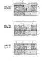
- FIGS. 1A to 1Eillustrate an example of a known process to manufacture a copper interconnect in a dielectric material.
- a previous line 3is formed in a previous dielectric layer 2 ′ made of a first dielectric material, e.g. silicon dioxide (SiO 2 ).
- the electrically conductive material of the previous line 3e.g. copper, is isolated from the silicon dioxide by a previous thin metallic barrier 7 ′.
- the thin metallic barrier 7 ′may comprise tantalum.
- a thin barrier of dielectric material 4is deposited on a surface of the previous dielectric layer 2 ′.
- a dielectric layer 2is deposited on the thin barrier of dielectric material 4 .
- the dielectric layermay also comprise silicon dioxide.
- the Dual Damascene processallows to form trenches 1 A , 1 B within the dielectric layer 2 . Lithographic operations are performed to set the zones to be etched. The dielectric layer is subsequently etched, using for example a reactive ion etching plasma (RIE plasma).
- FIG. 1Aillustrates a portion of a semiconductor device after such an etching operation.
- the etching or other patterning operationsmay damage a portion of the dielectric layer.
- the dielectric layermay comprise a damaged portion 8 on the walls of the trenches 1 A , 1 B .
- References 5 and 6correspond to cap layers, which serve as hard mask layers for patterning purposes or CMP (Chemical Mechanical Polishing) stop layers.
- the cap layersmay be left out in different integration schemes.
- the thin metallic barrier 7may comprise tantalum, or tantalum nitride.
- the thin metallic barrier 7allows for preventing copper atoms or copper ions of a further interconnect to diffuse into the dielectric layer 2 .
- copper 9is subsequently deposited so as to fill the trenches 1 A , 1 B .
- the depositingmay be performed in two steps (not represented). First, a copper seed layer is deposited on the thin metallic barrier, for example via a Physical Vapor Deposition (PVD). Then copper bulk is deposited on the copper seed layer via electroplating.
- PVDPhysical Vapor Deposition
- Polishing operationsallow for a leveling of the deposited copper 9 with the surface of the dielectric material, as shown in FIG. 1D .
- Masking layers 5 , 6may be removed by the polishing.
- the polishingmay for example be performed using a Chemical Mechanical Planarization (CMP).
- CMPChemical Mechanical Planarization
- a thin barrier 10 of dielectric materialmay subsequently be deposited on the polished surface.
- FIGS. 2A to 2G and FIGS. 3A to 3Billustrate exemplary embodiments of the present invention.
- a previous line 3is formed in a previous dielectric layer 2 ′ comprising a first dielectric material.
- the first dielectric materialmay comprise a porous ultra-low-k material.
- the porous ultra-low-k materialmay for example be made of carbon-incorporated silicon oxide (SiOC).
- the electrically conductive material of the previous line 3e.g. copper, is isolated from the SiOC by a previous thin metallic barrier 7 ′.
- the thin metallic barrier 7 ′may comprise tantalum, tantalum nitride or any other suitable metal material.
- a thin barrier of dielectric material 4is deposited on a surface of the previous dielectric layer 2 ′.
- a dielectric layer 2is deposited on the thin barrier of dielectric material 4 by plasma enhanced chemical vapor deposition (PECVD) or by any other deposition method.
- the dielectric layer 2may also comprise the porous SiOC ultra-low-k material.
- the dielectric layermay for example have a permittivity coefficient of 2.4.
- a Dual Damascene processallows to form trenches 1 A , 1 B within the dielectric layer 2 .
- Masking operations and lithographic operationsare performed to set the zones to be etched.
- the dielectric layeris subsequently etched, using for example a reactive ion etching plasma (RIE plasma).
- RIE plasmareactive ion etching plasma
- the trenchescomprise a first trench 1 A , corresponding to a further via, and a second trench 1 B , corresponding to a further line.
- a Dual Damascene processis performed, i.e. a single further deposition allows for the filling of the first trench 1 A and the second trench 1 B .
- each trenchis filled with copper before etching a new trench.
- each trenchis etched simultaneously on a surface of a semiconductor device, each trench corresponding to an interconnect.
- the etchingmay be followed by a stripping operation, and possibly by a wet cleaning operation.
- FIG. 2Aillustrates a portion of a semiconductor device after such patterning operations.
- References 5 and 6correspond to cap layers which serve as hard mask layers for patterning purposes or CMP stop layers.
- the cap layersmay be left out in different integration schemes.
- the patterning operationshave led to a deterioration of a portion 8 of the dielectric layer 2 .
- Pores of such a damaged portion 8may be sealed and the damaged portion 8 may exhibit higher density and permittivity than the rest of the dielectric layer 2 .
- the damaged portion 8may stretch out as far as 10 nm, 20 nm or 30 nm.
- the deteriorationmay partially transform the first dielectric material, i.e. SiOC, into a distinct dielectric material, e.g. SiO 2 .
- the removalis performed on side walls of the trenches 1 A , 1 B , i.e. substantially vertical walls 21 , 22 , 23 .
- the removalis also performed on a substantially horizontal wall 24 .
- the removingis performed selectively, using for example a Hydrogen Fluoride (HF) wet based solution.
- HFHydrogen Fluoride
- Such a selective wet etchingallows to remove the damaged dielectric material, i.e. SiO 2 , while leaving the first dielectric material, i.e. SiOC, unaffected.
- the removalis followed by a conformal deposition of a dielectric liner 12 made of a second dielectric material, as shown in FIG. 2C .
- the conformal depositingmay for example comprise a thermal Chemical Vapor Deposition (CVD) of a benzocyclobutene (BCB) liner.
- a BCB materialhas a permittivity coefficient of 2.7.
- liner materialse.g. SiOC, silicon carbide (SiC), SiO 2 or polyarylene ether (SiLK), may also be used.
- the dielectric liner 12is deposited on the side walls of the trenches 1 A , 1 B , thus allowing a proper sealing of pores of the dielectric layer between interconnects.
- the dielectric liner 12is also deposited on the previous line 3 and on the masking layers 5 , 6 .
- the conformal depositingis followed by a mask-less anisotropic etching, using for example fluoro carbon plasma etch (CF 4 /Ar or C 4 F 8 /Ar).
- CF 4 /Ar or C 4 F 8 /Arfluoro carbon plasma etch
- the anisotropic etchingallows to open up a bottom portion 13 of the deposited dielectric liner 12 , thus opening the copper of the previous line 3 , as shown in FIG. 2D .
- the anisotropic etchingalso allows for removal of surface portions 15 of the dielectric liner 12 , and overhangs 17 .
- a step portion 16 of the liner 12is also removed.
- a thin metallic barrier 14is subsequently deposited using a common metallization process, as shown in FIG. 2E .
- the thin metallic barrier 14may comprise tantalum, or tantalum nitride.
- the thin metallic barrier 14prevents copper atoms or copper ions of a further interconnect to diffuse into the dielectric liner 12 .
- the thin metallic barrier 14may contact the first dielectric material at a step zone corresponding to at least a portion of the removed step portion 16 .
- the anisotropic etchingprovides a densification of the ultra-low-k dielectric material at the step zone. The densification protects the porous ultra-low-k dielectric material from diffusion of metallic atoms or metallic ions.
- an intermediate stop layermay be used to protect the porous dielectric material from diffusion.
- the step zoneis not located between the further line portion 1 B and another further line portion (not represented) within the dielectric layer 2 .
- the interline capacitanceis hence relatively unaffected by a local increase of the permittivity.
- Copper 9may be deposited within the trenches, as shown in FIG. 2F .
- the depositingmay be performed in two steps (not represented). A copper seed layer is deposited and a copper bulk is subsequently deposited via electroplating.
- a polishing operationmay subsequently be performed so as to level the deposited copper with the dielectric layer 9 .
- the polishingmay also allow to remove the masking layers 5 , 6 .
- a thin barrier of dielectric material 10may subsequently be deposited on the polished surface, as shown in FIG. 2G .
- a further dielectric layermay be deposited so as to manufacture a new copper portion, e.g. a new line or a new via.
- the conformal depositing of the dielectric liner 12is followed by a conformal depositing of a thin metallic layer 14 , as shown in FIG. 3A .
- the thin metallic layer 14may possibly have a higher thickness at the bottom of the line 1 B than at the bottom of the via 1 A , depending on the deposition technique.
- a subsequent anisotropic etchingmay be performed, so as to open the previous line 3 (see, FIG. 3B ).
- PVDPhysical Vapor Deposition
- An etch rate variation or a sputtering rate variationallows to remove the metal barrier 14 and the dielectric liner 12 preferentially at the bottom of via 1 A.
- the liner 12may be removed at the bottom of the via 1 A and partially kept anywhere else in the structure, as shown in FIG. 3B .
- Such a tuning of the punch through processtherefore allows to open the bottom of the via 1 A while keeping protected substantially vertical and substantially horizontal walls of the dielectric layer 2 .
- Further operationsmay be performed so as to achieve an interconnect structure within the dielectric layer 2 .
- a subsequent metal barrier after punch through and copperare deposited within the trenches; a polishing operation is subsequently performed and a thin barrier of dielectric material is deposited on the polished surface.
Landscapes
- Engineering & Computer Science (AREA)
- Physics & Mathematics (AREA)
- Condensed Matter Physics & Semiconductors (AREA)
- General Physics & Mathematics (AREA)
- Manufacturing & Machinery (AREA)
- Computer Hardware Design (AREA)
- Microelectronics & Electronic Packaging (AREA)
- Power Engineering (AREA)
- Internal Circuitry In Semiconductor Integrated Circuit Devices (AREA)
- Drying Of Semiconductors (AREA)
Abstract
Description
- This application is a filing under 35 U.S.C. 371 of International Application No. PCT/IB2007/000455 filed Feb. 26, 2007, which claims priority from European Application No. 06290339.8 filed Feb. 28, 2006, the disclosures of which are hereby incorporated by reference.
- The present invention relates generally to the field of interconnects made of an electrically conductive material in a dielectric material, and more particularly but not exhaustively to metal interconnects in a dielectric material having a relatively low permittivity, i.e. low-k or ultra-low-k (ULK) materials.
- Such interconnects may be employed in semiconductor devices, e.g. integrated circuits (ICs).
- In conventional ICs, it is necessary to establish electrical contact between conductive layers that are formed on different levels of metallization and separated by dielectric layers.
- An IC interconnect may thus comprise vias and lines for interconnecting different parts of an underlying semiconductor substrate on which components, e.g. transistors, are formed. A line extends in a plane parallel to the plane of the semiconductor substrate. A via extends in a direction perpendicular to the plane of the semiconductor substrate, through a dielectric layer. Both the lines and the vias are formed by depositing electrically conductive material within a stack of patterned dielectric layers.
- Improvements in the performance of semiconductor devices (speed, low power consumption) have required a large number of changes of the materials that have been used up till now.
- In order to reduce the capacitance that exists between the lines formed in a layer of dielectric material, dielectric materials with a low permittivity coefficient “k”, typically lower than 4.2, or with an ultra-low-k, typically lower than 2.4, may be used. The interline capacitance is indeed proportional to the permittivity coefficient k of the dielectric material that is used. The ULK dielectric materials may comprise porous materials. The porous materials have a relatively low density.
- The improvements in the performance have also been achieved through the use of an electrically conductive material that is more conductive than aluminum, which has traditionally been used to make the interconnect lines. Copper, whose resistivity is nearly half that of aluminum doped with copper, has shown itself to be the best candidate.
- The use of ULK dielectric materials and copper allow for reduction in the capacitance C that exists between the lines and the resistance R of the interconnect respectively. The value of the propagation constant RC may hence be reduced. A semiconductor device with a propagation constant RC having a relatively low value may thus operate properly at relatively high frequencies; stated otherwise, the new materials allow for improvement in the performance of semiconductor devices.
- These new materials may be employed in the well-known Damascene or Dual Damascene processes. To obtain a metallization level n, a dielectric layer made of a first dielectric material is deposited on a layer of level n−1. Trenches are etched within the dielectric layer, the trenches corresponding to portions of the interconnect, e.g. lines and vias. A metallization operation, in which a thin metallic barrier is deposited, is performed and the electrically conductive material is subsequently deposited so as to fill the trenches and polished until it is level with the upper surface of the dielectric layer.
- The Damascene or Dual Damascene processes are well suited for producing copper lines and vias because, although copper has advantageous electrical properties for narrow lines, it cannot be etched at ambient temperature. Additionally, the Damascene and Dual Damascene processes may be used with other metals used to form lines and vias.
- During the Damascene or Dual Damascene processes, the etching of the trenches may be followed by other patterning operations such as stripping and cleaning. The stripping operation allows for removal of residues of photosensitive resin, and/or the residues of the etch chemistry. Wet cleaning operations may also be performed to remove contaminants.
- However, a patterning operation, i.e. etching, stripping and/or cleaning, may damage a portion of the dielectric layer. For example, cleaning solutions used for stripping etch residues may penetrate into the already damaged dielectric layer and provide an additional deterioration of the dielectric layer.
- In the case of porous dielectric materials, the dielectric layer may comprise a damaged portion on the walls of the trenches. The damaged portion may have a relatively large width, e.g. 10 or 20 nm.
- The permittivity of the damaged portion is higher than the permittivity of the first dielectric material, thus increasing a total permittivity of the etched dielectric layer. For example, the interline permittivity of a deposited dielectric layer may rise from 2.4 to 3.5 after the patterning operations. The interline capacitance being proportional to the overall permittivity, the damaging of the dielectric layer by the patterning operation leads to an increase of the interline capacitance and of the propagation constant RC.
- Furthermore, a porous dielectric material may be hydrophilic. If water molecules penetrate into the dielectric layer, the overall permittivity may also increase. The water molecules may also disturb the operation of the semiconductor device.
- Furthermore, metal containing precursor molecules used for a vapor deposition of the thin metallic barrier may diffuse into the pores of the porous dielectric layer, which may lead to a short circuit. If the thin metallic barrier has discontinuities, copper atoms or copper ions may also penetrate into the dielectric layer.
- There is thus a need for a dielectric layer having a small overall permittivity and in which the pores are protected from diffusion of water or metal molecules.
- It is known in the art to provide an intentional densification of the dielectric material on the side walls of the trench. The intentional densification may be performed after the etching, for example using a surface treatment or plasma bombardment.
- The densification provides a relative closing of the pores of the damaged portion. The relative closing of such peripheral pores allows avoiding diffusion of water and metal molecules.
- However, by locally increasing the dielectric permittivity, the intentional densification also increases the overall permittivity of the dielectric layer. Furthermore, a certain width is required for the damaged portion to protect the pores from diffusion. As the dimensions of the semiconductor devices shrink, the ratio between the volume of the damaged portion and the global volume of the etched dielectric layer increases, thus increasing the global permittivity of the dielectric layer and increasing the propagation constant RC.
- It is also known in the art to deposit a capping layer on the etched dielectric layer to protect the pores of the dielectric layer from diffusion. See, “O2-Plasma Degradation of Low-K Organic Dielectric and its Effective Solution for Damascene Trenches”, Ching-Fa Yeh et al., 2000 5thInternational Symposium on Plasma Process-Induced Damage, which describes such a capping operation.
- The capping layer may be made of a dielectric material having a relatively higher permittivity and a relatively higher density than the porous dielectric material of the dielectric layer. Hence, the capping layer allows to shield the pores from diffusion of water molecules or metal containing molecules, e.g. tantalum containing vapor used in atomic layer deposition (ALD) or chemical vapor deposition (CVD). The thin metallic barrier may subsequently be deposited on the capping layer without metallic deposition inside the porous dielectric material.
- However, the depositing of the capping layer reduces the volume to be filled with copper, which may cause problems in filling the trenches with copper. Furthermore, the resistivity of the interconnect may increase when the section of the interconnect becomes in the order of the mean free path of the electron. As the dimensions of the semiconductor devices shrink, the capping leads inevitably to an increase of the resistance of the interconnect, and thus to an increase of the value of the propagation constant RC.
- As a consequence, there is still a need for a semiconductor device comprising an interconnect made of an electrically conductive material in a dielectric layer and having a relatively low propagation constant value RC.
- In a first aspect, the present invention provides a method for manufacturing a semiconductor device comprising an interconnect comprising electrically conductive portions, in a dielectric layer made of a first dielectric material, said method comprising
- forming a trench in said dielectric layer;
- removing exposed portions of the dielectric layer which form the side walls of the trench; and
- depositing a dielectric liner on the side walls of the trench, the liner being made of a second dielectric material.
- The forming of the trench may comprise patterning operations, e.g. etching, stripping and/or wet cleaning, that may damage at least a portion of the dielectric layer. Such damaged portions are at least partially removed by the removing step and at least partially replaced by the deposited dielectric liner.
- The removal allows for avoiding an overall permittivity increase between the further interconnects, as may be the case if an intentional densification of the dielectric layer is performed on the side walls of the trench.
- Advantageously, the first dielectric material and the second dielectric material are distinct. The deposited dielectric liner may have satisfying low-k value and relatively good interaction properties with a further metallic barrier, thus achieving a proper pore sealing.
- The thickness of the deposited dielectric liner may be chosen so as to avoid a significant increase of an overall permittivity between the further interconnects, while assuring a proper protection of the pores of the dielectric layer. Also, the thickness of the deposited dielectric liner may be chosen to be smaller than or substantially equal to the thickness of the removed portions, so as to avoid reducing the volume to be filled with an electrically conductive material, as may be the case if a capping layer is deposited directly on the damaged dielectric layer. Furthermore, the control of the liner thickness may also allow one to control the section of the further interconnect.
- Also, several dielectric liners may be deposited. For example, a relatively porous dielectric liner may be deposited first, followed by a relatively dense dielectric liner. The relatively dense dielectric liner allows sealing the pores of the relatively porous dielectric liner and of the dielectric layer.
- More generally, several parameters, e.g. density, permittivity, thickness, etc. may be controlled, thus allowing a better control of the properties of the semiconductor device. Typically, the parameters may be chosen so as to provide a semiconductor device having a relatively low propagation constant value RC.
- Alternatively, the first dielectric material and the second dielectric material may be similar.
- The removing step may be performed immediately after the forming of the trench. Alternatively, one or more operations, e.g. an annealing operation, may be performed between the forming of the trench and the removing of exposed portions on side walls of the trench.
- The dielectric liner deposition may be performed immediately after the removal. Alternatively, one or more operations, e.g. an annealing operation, may be performed between the removal of exposed portions on side walls of the trench and the deposition of the dielectric liner on the side walls of the trench.
- Furthermore, the manufacturing method according to an aspect of the invention may involve well-known operations and products and is therefore relatively easy to achieve.
- Advantageously, the removing of the exposed portions of the dielectric layer comprises selectively removing damaged portions of the dielectric layer. Only the damaged portions are removed.
- For example, the removing of the damaged portion of the dielectric layer may be performed using a Hydrogen Fluoride (HF) based wet solution. The HF based wet solution may selectively dissolve the damaged portions of the dielectric layer, while leaving undamaged portions of the dielectric layer unaffected.
- Any other selective removal technique may be used.
- Alternatively, the removing may for example be time controlled, i.e. the removing operation is stopped after a determined duration. The duration may be determined experimentally, or theoretically, as allowing a total removal of the damaged portions.
- The depth of the removed portions may be controlled by any other method.
- The removing of the damaged portions may advantageously be total, so as to avoid leaving damaged zones. Alternatively, the damaged zones may be only partially removed.
- Advantageously, the manufacturing method further comprises providing an anisotropic etching of the deposited dielectric liner to open an underlying electrically conductive zone; and depositing a thin metallic barrier.
- The anisotropic etching allows etching a bottom portion of the deposited dielectric liner. The bottom portion of the deposited dielectric liner may indeed contact an electrically conductive zone, e.g. a contact point of a transistor, a via, or a line of the interconnect. The bottom portion of the deposited dielectric liner has to be removed to establish an electrical contact between said electrically conductive zone and a further electrically conductive portion, e.g. a via, of the interconnect.
- The anisotropic etching may leave the deposited dielectric liner on side walls of the trench.
- The anisotropic etching may also allow for removal of possible overhangs formed around masking layers. The anisotropic etching may possibly remove masking layers at a surface of the dielectric layer.
- Alternatively, a thin metallic barrier is deposited on the deposited dielectric liner. An anisotropic etching of the deposited thin metallic barrier and of the deposited dielectric liner is subsequently performed, so as to open the underlying electrically conductive zone. Such a punch through approach allows for removal of a bottom portion of the deposited thin metallic barrier and the bottom portion of the deposited dielectric liner, thus allowing an electrical contact between the electrically conductive zone and a further electrically conductive portion of the interconnect.
- Advantageously, a seed layer made of an electrically conductive material is deposited and a bulk made of the electrically conductive material is also deposited via electroplating.
- Alternatively, any other method allowing for filling of the trench with the electrically conductive material may be performed instead.
- Advantageously, a polishing operation may be performed to level the deposited electrically conductive material and a surface of the dielectric layer. Also, the polishing operation may allow for removal of possible masking layers.
- Alternatively, any other operation allowing for leveling of the deposited electrically conductive material and a surface of the dielectric layer may be performed.
- A thin barrier of dielectric material may or may not be deposited on the polished surface. The thin barrier of dielectric material may prevent diffusion of atoms or ions of the electrically conductive material into a further dielectric layer.
- Advantageously, the electrically conductive portions comprise copper, which is a relatively conductive material.
- However, any other electrically conductive material may be used.
- Advantageously, the permittivity of the first dielectric material may be lower than 4.2, or even lower than 2.4.
- Advantageously, the dielectric layer may comprise porous material.
- The first dielectric material may advantageously be selected from the group consisting of silicon dioxide (SiO2), carbon-incorporated silicon oxide (SiOC), oxycarbide (SiOCH), Fluorine doped silicate Glass (FSG), Phosphosilicate Glass (PSG) and boro-phospho-silicate glass (BPSG).
- However, any other suitable material may be employed as a first dielectric material.
- These and other aspects of the invention will be apparent from and elucidated with reference to the embodiments described hereinafter.
FIGS. 1A to 1E illustrate an example of a process to manufacture a copper interconnect in a dielectric layer according to Prior Art.FIGS. 2A to 2G illustrates an example of a manufacturing method according to a first embodiment of the present invention.FIGS. 3A and 3B illustrates an example of a manufacturing method according to a second embodiment of the present invention.- In all the figures, the same references denote similar or substantially similar elements.
FIGS. 1A to 1E illustrate an example of a known process to manufacture a copper interconnect in a dielectric material. In this example, aprevious line 3 is formed in a previousdielectric layer 2′ made of a first dielectric material, e.g. silicon dioxide (SiO2). The electrically conductive material of theprevious line 3, e.g. copper, is isolated from the silicon dioxide by a previous thinmetallic barrier 7′. The thinmetallic barrier 7′ may comprise tantalum.- A thin barrier of
dielectric material 4 is deposited on a surface of the previousdielectric layer 2′. - A
dielectric layer 2 is deposited on the thin barrier ofdielectric material 4. The dielectric layer may also comprise silicon dioxide. The Dual Damascene process allows to formtrenches dielectric layer 2. Lithographic operations are performed to set the zones to be etched. The dielectric layer is subsequently etched, using for example a reactive ion etching plasma (RIE plasma).FIG. 1A illustrates a portion of a semiconductor device after such an etching operation. - However, the etching or other patterning operations, such as stripping and/or cleaning, may damage a portion of the dielectric layer. The dielectric layer may comprise a damaged
portion 8 on the walls of thetrenches References - Alternatively, the cap layers may be left out in different integration schemes.
- A metallization operation, in which a thin
metallic barrier 7 is deposited, is subsequently performed, as illustrated inFIG. 1B . The thinmetallic barrier 7 may comprise tantalum, or tantalum nitride. The thinmetallic barrier 7 allows for preventing copper atoms or copper ions of a further interconnect to diffuse into thedielectric layer 2. - As illustrated in
FIG. 1C , copper9 is subsequently deposited so as to fill thetrenches - Polishing operations allow for a leveling of the deposited copper9 with the surface of the dielectric material, as shown in
FIG. 1D . Masking layers5,6 may be removed by the polishing. The polishing may for example be performed using a Chemical Mechanical Planarization (CMP). - As illustrated in
FIG. 1E , athin barrier 10 of dielectric material may subsequently be deposited on the polished surface. FIGS. 2A to 2G andFIGS. 3A to 3B illustrate exemplary embodiments of the present invention.- In the illustrated examples, a
previous line 3 is formed in a previousdielectric layer 2′ comprising a first dielectric material. The first dielectric material may comprise a porous ultra-low-k material. The porous ultra-low-k material may for example be made of carbon-incorporated silicon oxide (SiOC). The electrically conductive material of theprevious line 3, e.g. copper, is isolated from the SiOC by a previous thinmetallic barrier 7′. The thinmetallic barrier 7′ may comprise tantalum, tantalum nitride or any other suitable metal material. - A thin barrier of
dielectric material 4 is deposited on a surface of the previousdielectric layer 2′. - A
dielectric layer 2 is deposited on the thin barrier ofdielectric material 4 by plasma enhanced chemical vapor deposition (PECVD) or by any other deposition method. Thedielectric layer 2 may also comprise the porous SiOC ultra-low-k material. The dielectric layer may for example have a permittivity coefficient of 2.4. A Dual Damascene process allows to formtrenches dielectric layer 2. Masking operations and lithographic operations are performed to set the zones to be etched. The dielectric layer is subsequently etched, using for example a reactive ion etching plasma (RIE plasma). - In the illustrated examples, the trenches comprise a
first trench 1A, corresponding to a further via, and asecond trench 1B, corresponding to a further line. A Dual Damascene process is performed, i.e. a single further deposition allows for the filling of thefirst trench 1Aand thesecond trench 1B. - In alternative embodiments (not represented), each trench is filled with copper before etching a new trench.
- Typically, several trenches are etched simultaneously on a surface of a semiconductor device, each trench corresponding to an interconnect.
- The etching may be followed by a stripping operation, and possibly by a wet cleaning operation.
FIG. 2A illustrates a portion of a semiconductor device after such patterning operations.References - Alternatively, the cap layers may be left out in different integration schemes.
- The patterning operations have led to a deterioration of a
portion 8 of thedielectric layer 2. Pores of such a damagedportion 8 may be sealed and the damagedportion 8 may exhibit higher density and permittivity than the rest of thedielectric layer 2. The damagedportion 8 may stretch out as far as 10 nm, 20 nm or 30 nm. The deterioration may partially transform the first dielectric material, i.e. SiOC, into a distinct dielectric material, e.g. SiO2. - The exposed portions of the dielectric layer which form the side walls of the
trenches FIG. 2B . - The removal is performed on side walls of the
trenches vertical walls horizontal wall 24. - The removing is performed selectively, using for example a Hydrogen Fluoride (HF) wet based solution. Such a selective wet etching allows to remove the damaged dielectric material, i.e. SiO2, while leaving the first dielectric material, i.e. SiOC, unaffected.
- The removal is followed by a conformal deposition of a
dielectric liner 12 made of a second dielectric material, as shown inFIG. 2C . The conformal depositing may for example comprise a thermal Chemical Vapor Deposition (CVD) of a benzocyclobutene (BCB) liner. A BCB material has a permittivity coefficient of 2.7. - Other liner materials, e.g. SiOC, silicon carbide (SiC), SiO2or polyarylene ether (SiLK), may also be used.
- The
dielectric liner 12 is deposited on the side walls of thetrenches dielectric liner 12 is also deposited on theprevious line 3 and on the masking layers5,6. - In the first embodiment, the conformal depositing is followed by a mask-less anisotropic etching, using for example fluoro carbon plasma etch (CF4/Ar or C4F8/Ar). The anisotropic etching allows to open up a
bottom portion 13 of the depositeddielectric liner 12, thus opening the copper of theprevious line 3, as shown inFIG. 2D . - The anisotropic etching also allows for removal of
surface portions 15 of thedielectric liner 12, and overhangs17. - In this example, a
step portion 16 of theliner 12 is also removed. - A thin
metallic barrier 14 is subsequently deposited using a common metallization process, as shown inFIG. 2E . The thinmetallic barrier 14 may comprise tantalum, or tantalum nitride. The thinmetallic barrier 14 prevents copper atoms or copper ions of a further interconnect to diffuse into thedielectric liner 12. - The thin
metallic barrier 14 may contact the first dielectric material at a step zone corresponding to at least a portion of the removedstep portion 16. However, the anisotropic etching provides a densification of the ultra-low-k dielectric material at the step zone. The densification protects the porous ultra-low-k dielectric material from diffusion of metallic atoms or metallic ions. - Also, an intermediate stop layer may be used to protect the porous dielectric material from diffusion.
- Furthermore, the step zone is not located between the
further line portion 1Band another further line portion (not represented) within thedielectric layer 2. The interline capacitance is hence relatively unaffected by a local increase of the permittivity. - Copper9 may be deposited within the trenches, as shown in
FIG. 2F . The depositing may be performed in two steps (not represented). A copper seed layer is deposited and a copper bulk is subsequently deposited via electroplating. - A polishing operation may subsequently be performed so as to level the deposited copper with the dielectric layer9. The polishing may also allow to remove the masking layers5,6.
- A thin barrier of
dielectric material 10 may subsequently be deposited on the polished surface, as shown inFIG. 2G . - A further dielectric layer (not represented) may be deposited so as to manufacture a new copper portion, e.g. a new line or a new via.
- In the second embodiment, the conformal depositing of the
dielectric liner 12 is followed by a conformal depositing of a thinmetallic layer 14, as shown inFIG. 3A . - The thin
metallic layer 14 may possibly have a higher thickness at the bottom of theline 1Bthan at the bottom of the via1A, depending on the deposition technique. - A subsequent anisotropic etching may be performed, so as to open the previous line3 (see,
FIG. 3B ). - Such a punch through Physical Vapor Deposition (PVD) barrier process allows to remove surface portions of the thin
metallic layer 14 and thedielectric liner 12. - An etch rate variation or a sputtering rate variation allows to remove the
metal barrier 14 and thedielectric liner 12 preferentially at the bottom of via1A. Typically, theliner 12 may be removed at the bottom of the via1A and partially kept anywhere else in the structure, as shown inFIG. 3B . - Such a tuning of the punch through process therefore allows to open the bottom of the via1A while keeping protected substantially vertical and substantially horizontal walls of the
dielectric layer 2. - Further operations may be performed so as to achieve an interconnect structure within the
dielectric layer 2. Typically, a subsequent metal barrier after punch through and copper are deposited within the trenches; a polishing operation is subsequently performed and a thin barrier of dielectric material is deposited on the polished surface. - In the description above, it will be understood that when an element such as layer, region or substrate is referred to as being “on” or “onto” another element, the element is either directly on the other element, or intervening elements may also be present.
- Expressions such as “comprise”, “include”, “incorporate”, “contain”, “is” and “have” are to be construed in a non-exclusive manner when interpreting the description and its associated claims, namely construed to allow for other items or components which are not explicitly defined also to be present. Reference to the singular is also to be construed in be a reference to the plural and vice versa.
- A person skilled in the art will readily appreciate that various parameters disclosed in the description may be modified and that various embodiments disclosed and/or claimed may be combined without departing from the scope of the invention.
Claims (20)
Applications Claiming Priority (4)
| Application Number | Priority Date | Filing Date | Title |
|---|---|---|---|
| EP06290339.8 | 2006-02-28 | ||
| EP06290339 | 2006-02-28 | ||
| EP06290339 | 2006-02-28 | ||
| PCT/IB2007/000455WO2007099428A1 (en) | 2006-02-28 | 2007-02-26 | Metal interconnects in a dielectric material |
Publications (2)
| Publication Number | Publication Date |
|---|---|
| US20090218699A1true US20090218699A1 (en) | 2009-09-03 |
| US8138082B2 US8138082B2 (en) | 2012-03-20 |
Family
ID=38067583
Family Applications (1)
| Application Number | Title | Priority Date | Filing Date |
|---|---|---|---|
| US12/280,978ActiveUS8138082B2 (en) | 2006-02-28 | 2007-02-26 | Method for forming metal interconnects in a dielectric material |
Country Status (5)
| Country | Link |
|---|---|
| US (1) | US8138082B2 (en) |
| EP (1) | EP1989733A1 (en) |
| JP (1) | JP2009528690A (en) |
| CN (1) | CN101427361A (en) |
| WO (1) | WO2007099428A1 (en) |
Cited By (23)
| Publication number | Priority date | Publication date | Assignee | Title |
|---|---|---|---|---|
| US20100176513A1 (en)* | 2009-01-09 | 2010-07-15 | International Business Machines Corporation | Structure and method of forming metal interconnect structures in ultra low-k dielectrics |
| US20110049503A1 (en)* | 2008-10-29 | 2011-03-03 | Renesas Electronics Corporation | Semiconductor device and method for manufacturing the same |
| US20120199980A1 (en)* | 2011-02-07 | 2012-08-09 | Globalfoundries Inc. | Integrated circuits having interconnect structures and methods for fabricating integrated circuits having interconnect structures |
| US20130330935A1 (en)* | 2012-06-12 | 2013-12-12 | Bhadri Varadarajan | REMOTE PLASMA BASED DEPOSITION OF SiOC CLASS OF FILMS |
| US8846525B2 (en) | 2009-12-04 | 2014-09-30 | Novellus Systems, Inc. | Hardmask materials |
| US9123783B2 (en) | 2012-11-09 | 2015-09-01 | GlobalFoundries, Inc. | Integrated circuits and methods of forming integrated circuits with interlayer dielectric protection |
| US9234276B2 (en) | 2013-05-31 | 2016-01-12 | Novellus Systems, Inc. | Method to obtain SiC class of films of desired composition and film properties |
| US9337068B2 (en) | 2012-12-18 | 2016-05-10 | Lam Research Corporation | Oxygen-containing ceramic hard masks and associated wet-cleans |
| US9371579B2 (en) | 2013-10-24 | 2016-06-21 | Lam Research Corporation | Ground state hydrogen radical sources for chemical vapor deposition of silicon-carbon-containing films |
| US9837270B1 (en) | 2016-12-16 | 2017-12-05 | Lam Research Corporation | Densification of silicon carbide film using remote plasma treatment |
| US20170365462A1 (en)* | 2012-06-12 | 2017-12-21 | Novellus Systems, Inc. | Remote plasma based deposition of oxygen doped silicon carbide films |
| US10002787B2 (en) | 2016-11-23 | 2018-06-19 | Lam Research Corporation | Staircase encapsulation in 3D NAND fabrication |
| US20180358284A1 (en)* | 2012-12-31 | 2018-12-13 | International Business Machines Corporation | Phase changing on-chip thermal heat sink |
| US10297442B2 (en) | 2013-05-31 | 2019-05-21 | Lam Research Corporation | Remote plasma based deposition of graded or multi-layered silicon carbide film |
| US10325773B2 (en) | 2012-06-12 | 2019-06-18 | Novellus Systems, Inc. | Conformal deposition of silicon carbide films |
| US20200075457A1 (en)* | 2018-08-28 | 2020-03-05 | Wuhan Xinxin Semiconductor Manufacturing Co., Ltd. | Semiconductor device and fabrication method thereof |
| US10840087B2 (en) | 2018-07-20 | 2020-11-17 | Lam Research Corporation | Remote plasma based deposition of boron nitride, boron carbide, and boron carbonitride films |
| US11049716B2 (en) | 2015-04-21 | 2021-06-29 | Lam Research Corporation | Gap fill using carbon-based films |
| US20220028797A1 (en)* | 2019-09-28 | 2022-01-27 | International Business Machines Corporation | Bottom Barrier Free Interconnects Without Voids |
| US11335720B2 (en)* | 2016-12-26 | 2022-05-17 | Sony Semiconductor Solutions Corporation | Vertical electrode structure comprising low-resistance film for preventing damage during etching |
| US11848199B2 (en) | 2018-10-19 | 2023-12-19 | Lam Research Corporation | Doped or undoped silicon carbide deposition and remote hydrogen plasma exposure for gapfill |
| US12334332B2 (en) | 2012-06-12 | 2025-06-17 | Lam Research Corporation | Remote plasma based deposition of silicon carbide films using silicon-containing and carbon-containing precursors |
| US12359311B2 (en) | 2012-06-12 | 2025-07-15 | Lam Research Corporation | Conformal deposition of silicon carbide films using heterogeneous precursor interaction |
Families Citing this family (12)
| Publication number | Priority date | Publication date | Assignee | Title |
|---|---|---|---|---|
| US7846834B2 (en)* | 2008-02-04 | 2010-12-07 | International Business Machines Corporation | Interconnect structure and method for Cu/ultra low k integration |
| DE102008054068A1 (en)* | 2008-10-31 | 2010-06-24 | Advanced Micro Devices, Inc., Sunnyvale | Narrowing metal cavities in a metallic layer stack of a semiconductor device by providing a dielectric barrier layer |
| JP2010171081A (en)* | 2009-01-20 | 2010-08-05 | Toshiba Corp | Semiconductor device and manufacturing method thereof |
| JP5173863B2 (en)* | 2009-01-20 | 2013-04-03 | パナソニック株式会社 | Semiconductor device and manufacturing method thereof |
| CN102468223A (en)* | 2010-11-16 | 2012-05-23 | 中芯国际集成电路制造(上海)有限公司 | Method for forming contact hole |
| US8623468B2 (en)* | 2012-01-05 | 2014-01-07 | Taiwan Semiconductor Manufacturing Company, Ltd. | Methods of fabricating metal hard masks |
| CN105097656B (en)* | 2014-05-08 | 2018-05-04 | 中芯国际集成电路制造(上海)有限公司 | A kind of semiconductor devices and preparation method thereof, electronic device |
| US9583386B2 (en)* | 2014-10-25 | 2017-02-28 | Lam Research Corporation | Interlevel conductor pre-fill utilizing selective barrier deposition |
| US10985055B2 (en) | 2015-12-30 | 2021-04-20 | Taiwan Semiconductor Manufacturing Co., Ltd. | Interconnection structure with anti-adhesion layer |
| US10629478B2 (en) | 2017-08-22 | 2020-04-21 | International Business Machines Corporation | Dual-damascene formation with dielectric spacer and thin liner |
| US11096271B1 (en)* | 2020-04-09 | 2021-08-17 | Raytheon Company | Double-sided, high-density network fabrication |
| CN112018079B (en)* | 2020-07-29 | 2022-10-25 | 复旦大学 | Copper interconnection structure and preparation method thereof |
Citations (8)
| Publication number | Priority date | Publication date | Assignee | Title |
|---|---|---|---|---|
| US6297333B1 (en)* | 1995-07-17 | 2001-10-02 | Mitsui Chemicals Inc | Olefin polymerization catalyst, process for preparing olefin polymer, and olefin polymer |
| US20030116854A1 (en)* | 2001-12-26 | 2003-06-26 | Kabushiki Kaisha Toshiba | Semiconductor device and method for manufacturing the same |
| US20040092095A1 (en)* | 2002-11-12 | 2004-05-13 | Applied Materials, Inc. | Side wall passivation films for damascene cu/low k electronic devices |
| US20040135255A1 (en)* | 2003-01-09 | 2004-07-15 | Noriaki Matsunaga | Semiconductor device and its manufacturing method |
| US20050148202A1 (en)* | 2002-06-20 | 2005-07-07 | Ludger Heiliger | Method for sealing porous materials during chip production and compounds therefor |
| US20070202676A1 (en)* | 2006-02-24 | 2007-08-30 | Taiwan Semiconductor Manufacturing Company, Ltd. | Integration scheme for cu/low-k interconnects |
| US7338893B2 (en)* | 2005-11-23 | 2008-03-04 | Texas Instruments Incorporated | Integration of pore sealing liner into dual-damascene methods and devices |
| US7651942B2 (en)* | 2005-08-15 | 2010-01-26 | Infineon Technologies Ag | Metal interconnect structure and method |
Family Cites Families (4)
| Publication number | Priority date | Publication date | Assignee | Title |
|---|---|---|---|---|
| TW486801B (en) | 2000-04-07 | 2002-05-11 | Taiwan Semiconductor Mfg | Method of fabricating dual damascene structure |
| JP3898669B2 (en)* | 2002-06-10 | 2007-03-28 | 株式会社東芝 | Manufacturing method of semiconductor device |
| DE10227663A1 (en)* | 2002-06-20 | 2004-01-15 | Infineon Technologies Ag | Process for sealing porous materials in chip manufacture and connections therefor |
| WO2004107434A1 (en)* | 2003-05-29 | 2004-12-09 | Nec Corporation | Wiring structure and method for producing same |
- 2007
- 2007-02-26WOPCT/IB2007/000455patent/WO2007099428A1/enactiveApplication Filing
- 2007-02-26JPJP2008556867Apatent/JP2009528690A/enactivePending
- 2007-02-26EPEP07713067Apatent/EP1989733A1/ennot_activeWithdrawn
- 2007-02-26CNCNA2007800070248Apatent/CN101427361A/enactivePending
- 2007-02-26USUS12/280,978patent/US8138082B2/enactiveActive
Patent Citations (8)
| Publication number | Priority date | Publication date | Assignee | Title |
|---|---|---|---|---|
| US6297333B1 (en)* | 1995-07-17 | 2001-10-02 | Mitsui Chemicals Inc | Olefin polymerization catalyst, process for preparing olefin polymer, and olefin polymer |
| US20030116854A1 (en)* | 2001-12-26 | 2003-06-26 | Kabushiki Kaisha Toshiba | Semiconductor device and method for manufacturing the same |
| US20050148202A1 (en)* | 2002-06-20 | 2005-07-07 | Ludger Heiliger | Method for sealing porous materials during chip production and compounds therefor |
| US20040092095A1 (en)* | 2002-11-12 | 2004-05-13 | Applied Materials, Inc. | Side wall passivation films for damascene cu/low k electronic devices |
| US20040135255A1 (en)* | 2003-01-09 | 2004-07-15 | Noriaki Matsunaga | Semiconductor device and its manufacturing method |
| US7651942B2 (en)* | 2005-08-15 | 2010-01-26 | Infineon Technologies Ag | Metal interconnect structure and method |
| US7338893B2 (en)* | 2005-11-23 | 2008-03-04 | Texas Instruments Incorporated | Integration of pore sealing liner into dual-damascene methods and devices |
| US20070202676A1 (en)* | 2006-02-24 | 2007-08-30 | Taiwan Semiconductor Manufacturing Company, Ltd. | Integration scheme for cu/low-k interconnects |
Cited By (38)
| Publication number | Priority date | Publication date | Assignee | Title |
|---|---|---|---|---|
| US20110049503A1 (en)* | 2008-10-29 | 2011-03-03 | Renesas Electronics Corporation | Semiconductor device and method for manufacturing the same |
| US8164196B2 (en)* | 2008-10-29 | 2012-04-24 | Renesas Electronics Corporation | Semiconductor device and method for manufacturing the same |
| US20100176513A1 (en)* | 2009-01-09 | 2010-07-15 | International Business Machines Corporation | Structure and method of forming metal interconnect structures in ultra low-k dielectrics |
| US8846525B2 (en) | 2009-12-04 | 2014-09-30 | Novellus Systems, Inc. | Hardmask materials |
| US20120199980A1 (en)* | 2011-02-07 | 2012-08-09 | Globalfoundries Inc. | Integrated circuits having interconnect structures and methods for fabricating integrated circuits having interconnect structures |
| US20170365462A1 (en)* | 2012-06-12 | 2017-12-21 | Novellus Systems, Inc. | Remote plasma based deposition of oxygen doped silicon carbide films |
| US10832904B2 (en)* | 2012-06-12 | 2020-11-10 | Lam Research Corporation | Remote plasma based deposition of oxygen doped silicon carbide films |
| US12359311B2 (en) | 2012-06-12 | 2025-07-15 | Lam Research Corporation | Conformal deposition of silicon carbide films using heterogeneous precursor interaction |
| US11264234B2 (en) | 2012-06-12 | 2022-03-01 | Novellus Systems, Inc. | Conformal deposition of silicon carbide films |
| US12334332B2 (en) | 2012-06-12 | 2025-06-17 | Lam Research Corporation | Remote plasma based deposition of silicon carbide films using silicon-containing and carbon-containing precursors |
| TWI571932B (en)* | 2012-06-12 | 2017-02-21 | 諾發系統有限公司 | Remote plasma based deposition using SiOC films |
| US12272547B2 (en) | 2012-06-12 | 2025-04-08 | Novellus Systems, Inc. | Conformal deposition of silicon carbide films |
| US10325773B2 (en) | 2012-06-12 | 2019-06-18 | Novellus Systems, Inc. | Conformal deposition of silicon carbide films |
| US11894227B2 (en) | 2012-06-12 | 2024-02-06 | Novellus Systems, Inc. | Conformal deposition of silicon carbide films |
| US20130330935A1 (en)* | 2012-06-12 | 2013-12-12 | Bhadri Varadarajan | REMOTE PLASMA BASED DEPOSITION OF SiOC CLASS OF FILMS |
| US10211310B2 (en)* | 2012-06-12 | 2019-02-19 | Novellus Systems, Inc. | Remote plasma based deposition of SiOC class of films |
| US9123783B2 (en) | 2012-11-09 | 2015-09-01 | GlobalFoundries, Inc. | Integrated circuits and methods of forming integrated circuits with interlayer dielectric protection |
| US9337068B2 (en) | 2012-12-18 | 2016-05-10 | Lam Research Corporation | Oxygen-containing ceramic hard masks and associated wet-cleans |
| US20180358284A1 (en)* | 2012-12-31 | 2018-12-13 | International Business Machines Corporation | Phase changing on-chip thermal heat sink |
| US11680314B2 (en) | 2013-05-31 | 2023-06-20 | Novellus Systems, Inc. | Films of desired composition and film properties |
| US11680315B2 (en) | 2013-05-31 | 2023-06-20 | Novellus Systems, Inc. | Films of desired composition and film properties |
| US9234276B2 (en) | 2013-05-31 | 2016-01-12 | Novellus Systems, Inc. | Method to obtain SiC class of films of desired composition and film properties |
| US11732350B2 (en) | 2013-05-31 | 2023-08-22 | Novellus Systems, Inc. | Films of desired composition and film properties |
| US10472714B2 (en) | 2013-05-31 | 2019-11-12 | Novellus Systems, Inc. | Method to obtain SiC class of films of desired composition and film properties |
| US11708634B2 (en) | 2013-05-31 | 2023-07-25 | Novellus Systems, Inc. | Films of desired composition and film properties |
| US10297442B2 (en) | 2013-05-31 | 2019-05-21 | Lam Research Corporation | Remote plasma based deposition of graded or multi-layered silicon carbide film |
| US9371579B2 (en) | 2013-10-24 | 2016-06-21 | Lam Research Corporation | Ground state hydrogen radical sources for chemical vapor deposition of silicon-carbon-containing films |
| US11049716B2 (en) | 2015-04-21 | 2021-06-29 | Lam Research Corporation | Gap fill using carbon-based films |
| US10002787B2 (en) | 2016-11-23 | 2018-06-19 | Lam Research Corporation | Staircase encapsulation in 3D NAND fabrication |
| US10580690B2 (en) | 2016-11-23 | 2020-03-03 | Lam Research Corporation | Staircase encapsulation in 3D NAND fabrication |
| US9837270B1 (en) | 2016-12-16 | 2017-12-05 | Lam Research Corporation | Densification of silicon carbide film using remote plasma treatment |
| US11335720B2 (en)* | 2016-12-26 | 2022-05-17 | Sony Semiconductor Solutions Corporation | Vertical electrode structure comprising low-resistance film for preventing damage during etching |
| US10840087B2 (en) | 2018-07-20 | 2020-11-17 | Lam Research Corporation | Remote plasma based deposition of boron nitride, boron carbide, and boron carbonitride films |
| US20200075457A1 (en)* | 2018-08-28 | 2020-03-05 | Wuhan Xinxin Semiconductor Manufacturing Co., Ltd. | Semiconductor device and fabrication method thereof |
| US11848199B2 (en) | 2018-10-19 | 2023-12-19 | Lam Research Corporation | Doped or undoped silicon carbide deposition and remote hydrogen plasma exposure for gapfill |
| US12300488B2 (en) | 2018-10-19 | 2025-05-13 | Lam Research Corporation | Doped or undoped silicon carbide deposition and remote hydrogen plasma exposure for gapfill |
| US20220028797A1 (en)* | 2019-09-28 | 2022-01-27 | International Business Machines Corporation | Bottom Barrier Free Interconnects Without Voids |
| US12266607B2 (en)* | 2019-09-28 | 2025-04-01 | International Business Machines Corporation | Bottom barrier free interconnects without voids |
Also Published As
| Publication number | Publication date |
|---|---|
| US8138082B2 (en) | 2012-03-20 |
| CN101427361A (en) | 2009-05-06 |
| WO2007099428A1 (en) | 2007-09-07 |
| JP2009528690A (en) | 2009-08-06 |
| EP1989733A1 (en) | 2008-11-12 |
Similar Documents
| Publication | Publication Date | Title |
|---|---|---|
| US8138082B2 (en) | Method for forming metal interconnects in a dielectric material | |
| CN100576494C (en) | Method for forming dual damascene wiring of semiconductor device using protective via capping layer | |
| US7550822B2 (en) | Dual-damascene metal wiring patterns for integrated circuit devices | |
| US6744090B2 (en) | Damascene capacitor formed in metal interconnection layer | |
| US6972253B2 (en) | Method for forming dielectric barrier layer in damascene structure | |
| US20040232552A1 (en) | Air gap dual damascene process and structure | |
| US8791013B2 (en) | Pattern forming method | |
| US7338893B2 (en) | Integration of pore sealing liner into dual-damascene methods and devices | |
| US7566656B2 (en) | Method and apparatus for providing void structures | |
| US8822342B2 (en) | Method to reduce depth delta between dense and wide features in dual damascene structures | |
| US20070232048A1 (en) | Damascene interconnection having a SiCOH low k layer | |
| US7052990B2 (en) | Sealed pores in low-k material damascene conductive structures | |
| US20080171442A1 (en) | Metal interconnect structure and process for forming same | |
| US20120199980A1 (en) | Integrated circuits having interconnect structures and methods for fabricating integrated circuits having interconnect structures | |
| JP5047504B2 (en) | Method for manufacturing dual damascene wiring of semiconductor device using via capping protective film | |
| KR20050114784A (en) | Method for forming cu interconnection of semiconductor device | |
| CN108573912B (en) | Semiconductor structure and forming method thereof | |
| KR100552815B1 (en) | Dual damascene wiring formation method of semiconductor device | |
| US6403471B1 (en) | Method of forming a dual damascene structure including smoothing the top part of a via | |
| US20070273027A1 (en) | Method of forming dual damascene pattern | |
| US7326632B2 (en) | Method for fabricating metal wirings of semiconductor device | |
| US8048799B2 (en) | Method for forming copper wiring in semiconductor device | |
| KR100731085B1 (en) | Copper wiring formation method using dual damascene process | |
| KR100483838B1 (en) | Dual damascene process of metal wire | |
| KR20070033175A (en) | Metal wiring formation method of semiconductor device |
Legal Events
| Date | Code | Title | Description |
|---|---|---|---|
| AS | Assignment | Owner name:STMICROELECTRONICS (CROLLES 2) SAS, FRANCE Free format text:ASSIGNMENT OF ASSIGNORS INTEREST;ASSIGNORS:TORRES, JOAQUIN;ARNAL, VINCENT;GOSSET, LAURENT-GEORGES;AND OTHERS;REEL/FRAME:022454/0455;SIGNING DATES FROM 20090201 TO 20090226 Owner name:KONINKLJKE PHILIPS ELECTRONICS N.V., NETHERLANDS Free format text:ASSIGNMENT OF ASSIGNORS INTEREST;ASSIGNORS:TORRES, JOAQUIN;ARNAL, VINCENT;GOSSET, LAURENT-GEORGES;AND OTHERS;REEL/FRAME:022454/0455;SIGNING DATES FROM 20090201 TO 20090226 Owner name:STMICROELECTRONICS (CROLLES 2) SAS, FRANCE Free format text:ASSIGNMENT OF ASSIGNORS INTEREST;ASSIGNORS:TORRES, JOAQUIN;ARNAL, VINCENT;GOSSET, LAURENT-GEORGES;AND OTHERS;SIGNING DATES FROM 20090201 TO 20090226;REEL/FRAME:022454/0455 Owner name:KONINKLJKE PHILIPS ELECTRONICS N.V., NETHERLANDS Free format text:ASSIGNMENT OF ASSIGNORS INTEREST;ASSIGNORS:TORRES, JOAQUIN;ARNAL, VINCENT;GOSSET, LAURENT-GEORGES;AND OTHERS;SIGNING DATES FROM 20090201 TO 20090226;REEL/FRAME:022454/0455 | |
| AS | Assignment | Owner name:NXP B.V.,NETHERLANDS Free format text:ASSIGNMENT OF ASSIGNORS INTEREST;ASSIGNOR:KONINKLIJKE PHILIPS ELECTRONICS N.V.;REEL/FRAME:022597/0832 Effective date:20090409 Owner name:NXP B.V., NETHERLANDS Free format text:ASSIGNMENT OF ASSIGNORS INTEREST;ASSIGNOR:KONINKLIJKE PHILIPS ELECTRONICS N.V.;REEL/FRAME:022597/0832 Effective date:20090409 | |
| STCF | Information on status: patent grant | Free format text:PATENTED CASE | |
| AS | Assignment | Owner name:STMICROELECTRONICS (CROLLES 2) SAS, FRANCE Free format text:ASSIGNMENT OF ASSIGNORS INTEREST;ASSIGNOR:NXP B.V.;REEL/FRAME:031089/0084 Effective date:20130411 | |
| FPAY | Fee payment | Year of fee payment:4 | |
| MAFP | Maintenance fee payment | Free format text:PAYMENT OF MAINTENANCE FEE, 8TH YEAR, LARGE ENTITY (ORIGINAL EVENT CODE: M1552); ENTITY STATUS OF PATENT OWNER: LARGE ENTITY Year of fee payment:8 | |
| MAFP | Maintenance fee payment | Free format text:PAYMENT OF MAINTENANCE FEE, 12TH YEAR, LARGE ENTITY (ORIGINAL EVENT CODE: M1553); ENTITY STATUS OF PATENT OWNER: LARGE ENTITY Year of fee payment:12 |