US20090218603A1 - Semiconductor device structures and methods of forming semiconductor structures - Google Patents
Semiconductor device structures and methods of forming semiconductor structuresDownload PDFInfo
- Publication number
- US20090218603A1 US20090218603A1US12/463,309US46330909AUS2009218603A1US 20090218603 A1US20090218603 A1US 20090218603A1US 46330909 AUS46330909 AUS 46330909AUS 2009218603 A1US2009218603 A1US 2009218603A1
- Authority
- US
- United States
- Prior art keywords
- semiconductor body
- silicon
- sidewalls
- silicon film
- hard mask
- Prior art date
- Legal status (The legal status is an assumption and is not a legal conclusion. Google has not performed a legal analysis and makes no representation as to the accuracy of the status listed.)
- Granted
Links
Images


Classifications
- H—ELECTRICITY
- H10—SEMICONDUCTOR DEVICES; ELECTRIC SOLID-STATE DEVICES NOT OTHERWISE PROVIDED FOR
- H10D—INORGANIC ELECTRIC SEMICONDUCTOR DEVICES
- H10D30/00—Field-effect transistors [FET]
- H10D30/60—Insulated-gate field-effect transistors [IGFET]
- H10D30/62—Fin field-effect transistors [FinFET]
- H10D30/6212—Fin field-effect transistors [FinFET] having fin-shaped semiconductor bodies having non-rectangular cross-sections
- H—ELECTRICITY
- H01—ELECTRIC ELEMENTS
- H01L—SEMICONDUCTOR DEVICES NOT COVERED BY CLASS H10
- H01L21/00—Processes or apparatus adapted for the manufacture or treatment of semiconductor or solid state devices or of parts thereof
- H01L21/02—Manufacture or treatment of semiconductor devices or of parts thereof
- H01L21/04—Manufacture or treatment of semiconductor devices or of parts thereof the devices having potential barriers, e.g. a PN junction, depletion layer or carrier concentration layer
- H01L21/18—Manufacture or treatment of semiconductor devices or of parts thereof the devices having potential barriers, e.g. a PN junction, depletion layer or carrier concentration layer the devices having semiconductor bodies comprising elements of Group IV of the Periodic Table or AIIIBV compounds with or without impurities, e.g. doping materials
- H01L21/30—Treatment of semiconductor bodies using processes or apparatus not provided for in groups H01L21/20 - H01L21/26
- H01L21/302—Treatment of semiconductor bodies using processes or apparatus not provided for in groups H01L21/20 - H01L21/26 to change their surface-physical characteristics or shape, e.g. etching, polishing, cutting
- H01L21/306—Chemical or electrical treatment, e.g. electrolytic etching
- H01L21/30604—Chemical etching
- H01L21/30608—Anisotropic liquid etching
- H—ELECTRICITY
- H01—ELECTRIC ELEMENTS
- H01L—SEMICONDUCTOR DEVICES NOT COVERED BY CLASS H10
- H01L21/00—Processes or apparatus adapted for the manufacture or treatment of semiconductor or solid state devices or of parts thereof
- H01L21/02—Manufacture or treatment of semiconductor devices or of parts thereof
- H01L21/04—Manufacture or treatment of semiconductor devices or of parts thereof the devices having potential barriers, e.g. a PN junction, depletion layer or carrier concentration layer
- H01L21/18—Manufacture or treatment of semiconductor devices or of parts thereof the devices having potential barriers, e.g. a PN junction, depletion layer or carrier concentration layer the devices having semiconductor bodies comprising elements of Group IV of the Periodic Table or AIIIBV compounds with or without impurities, e.g. doping materials
- H01L21/30—Treatment of semiconductor bodies using processes or apparatus not provided for in groups H01L21/20 - H01L21/26
- H01L21/302—Treatment of semiconductor bodies using processes or apparatus not provided for in groups H01L21/20 - H01L21/26 to change their surface-physical characteristics or shape, e.g. etching, polishing, cutting
- H01L21/306—Chemical or electrical treatment, e.g. electrolytic etching
- H01L21/30604—Chemical etching
- H01L21/30612—Etching of AIIIBV compounds
- H01L21/30617—Anisotropic liquid etching
- H—ELECTRICITY
- H01—ELECTRIC ELEMENTS
- H01L—SEMICONDUCTOR DEVICES NOT COVERED BY CLASS H10
- H01L21/00—Processes or apparatus adapted for the manufacture or treatment of semiconductor or solid state devices or of parts thereof
- H01L21/02—Manufacture or treatment of semiconductor devices or of parts thereof
- H01L21/04—Manufacture or treatment of semiconductor devices or of parts thereof the devices having potential barriers, e.g. a PN junction, depletion layer or carrier concentration layer
- H01L21/18—Manufacture or treatment of semiconductor devices or of parts thereof the devices having potential barriers, e.g. a PN junction, depletion layer or carrier concentration layer the devices having semiconductor bodies comprising elements of Group IV of the Periodic Table or AIIIBV compounds with or without impurities, e.g. doping materials
- H01L21/30—Treatment of semiconductor bodies using processes or apparatus not provided for in groups H01L21/20 - H01L21/26
- H01L21/302—Treatment of semiconductor bodies using processes or apparatus not provided for in groups H01L21/20 - H01L21/26 to change their surface-physical characteristics or shape, e.g. etching, polishing, cutting
- H01L21/306—Chemical or electrical treatment, e.g. electrolytic etching
- H01L21/308—Chemical or electrical treatment, e.g. electrolytic etching using masks
- H01L21/3083—Chemical or electrical treatment, e.g. electrolytic etching using masks characterised by their size, orientation, disposition, behaviour, shape, in horizontal or vertical plane
- H01L21/3085—Chemical or electrical treatment, e.g. electrolytic etching using masks characterised by their size, orientation, disposition, behaviour, shape, in horizontal or vertical plane characterised by their behaviour during the process, e.g. soluble masks, redeposited masks
- H—ELECTRICITY
- H10—SEMICONDUCTOR DEVICES; ELECTRIC SOLID-STATE DEVICES NOT OTHERWISE PROVIDED FOR
- H10D—INORGANIC ELECTRIC SEMICONDUCTOR DEVICES
- H10D30/00—Field-effect transistors [FET]
- H10D30/01—Manufacture or treatment
- H10D30/021—Manufacture or treatment of FETs having insulated gates [IGFET]
- H10D30/024—Manufacture or treatment of FETs having insulated gates [IGFET] of fin field-effect transistors [FinFET]
- H—ELECTRICITY
- H10—SEMICONDUCTOR DEVICES; ELECTRIC SOLID-STATE DEVICES NOT OTHERWISE PROVIDED FOR
- H10D—INORGANIC ELECTRIC SEMICONDUCTOR DEVICES
- H10D62/00—Semiconductor bodies, or regions thereof, of devices having potential barriers
- H10D62/10—Shapes, relative sizes or dispositions of the regions of the semiconductor bodies; Shapes of the semiconductor bodies
- H10D62/117—Shapes of semiconductor bodies
- H—ELECTRICITY
- H10—SEMICONDUCTOR DEVICES; ELECTRIC SOLID-STATE DEVICES NOT OTHERWISE PROVIDED FOR
- H10D—INORGANIC ELECTRIC SEMICONDUCTOR DEVICES
- H10D62/00—Semiconductor bodies, or regions thereof, of devices having potential barriers
- H10D62/40—Crystalline structures
- H—ELECTRICITY
- H10—SEMICONDUCTOR DEVICES; ELECTRIC SOLID-STATE DEVICES NOT OTHERWISE PROVIDED FOR
- H10D—INORGANIC ELECTRIC SEMICONDUCTOR DEVICES
- H10D62/00—Semiconductor bodies, or regions thereof, of devices having potential barriers
- H10D62/40—Crystalline structures
- H10D62/405—Orientations of crystalline planes
- H—ELECTRICITY
- H10—SEMICONDUCTOR DEVICES; ELECTRIC SOLID-STATE DEVICES NOT OTHERWISE PROVIDED FOR
- H10D—INORGANIC ELECTRIC SEMICONDUCTOR DEVICES
- H10D64/00—Electrodes of devices having potential barriers
- H10D64/60—Electrodes characterised by their materials
- H10D64/66—Electrodes having a conductor capacitively coupled to a semiconductor by an insulator, e.g. MIS electrodes
- H10D64/68—Electrodes having a conductor capacitively coupled to a semiconductor by an insulator, e.g. MIS electrodes characterised by the insulator, e.g. by the gate insulator
- H—ELECTRICITY
- H10—SEMICONDUCTOR DEVICES; ELECTRIC SOLID-STATE DEVICES NOT OTHERWISE PROVIDED FOR
- H10D—INORGANIC ELECTRIC SEMICONDUCTOR DEVICES
- H10D86/00—Integrated devices formed in or on insulating or conducting substrates, e.g. formed in silicon-on-insulator [SOI] substrates or on stainless steel or glass substrates
- H10D86/01—Manufacture or treatment
- H—ELECTRICITY
- H10—SEMICONDUCTOR DEVICES; ELECTRIC SOLID-STATE DEVICES NOT OTHERWISE PROVIDED FOR
- H10D—INORGANIC ELECTRIC SEMICONDUCTOR DEVICES
- H10D30/00—Field-effect transistors [FET]
- H10D30/60—Insulated-gate field-effect transistors [IGFET]
- H10D30/67—Thin-film transistors [TFT]
- H10D30/674—Thin-film transistors [TFT] characterised by the active materials
- H10D30/6741—Group IV materials, e.g. germanium or silicon carbide
- H—ELECTRICITY
- H10—SEMICONDUCTOR DEVICES; ELECTRIC SOLID-STATE DEVICES NOT OTHERWISE PROVIDED FOR
- H10D—INORGANIC ELECTRIC SEMICONDUCTOR DEVICES
- H10D30/00—Field-effect transistors [FET]
- H10D30/60—Insulated-gate field-effect transistors [IGFET]
- H10D30/67—Thin-film transistors [TFT]
- H10D30/674—Thin-film transistors [TFT] characterised by the active materials
- H10D30/675—Group III-V materials, Group II-VI materials, Group IV-VI materials, selenium or tellurium
Definitions
- the present inventionrelates to the field of semiconductor processing and more particularly to semiconductor structures and their methods of fabrication.
- SOI transistorsIn order to increase the performance of modern integrated circuits, such as microprocessors, silicon on insulator (SOI) transistors have been proposed. Silicon on insulator (SOI) transistors have an advantage in that they can be operated in a fully depleted manner. Fully depleted transistors have an advantage of ideal subthreshold gradients for optimized on current/off current ratios.
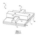
- An example of a proposed SOI transistor which can be operated in a fully depleted manneris that of a tri-gate transistor 100 , such as illustrated in FIG. 1 .
- Tri-gate transistor 100includes a silicon body 104 formed on insulating substrate 102 having buried oxide layer 103 formed on a monocrystalline silicon substrate 105 .
- a gate dielectric layer 106is formed on the top and sidewalls of the silicon body 104 as shown in FIG. 1 .
- a gate electrode 108is formed on the gate dielectric layer and surrounds the body 104 on three sides essentially providing a transistor 100 having three gate electrodes (G 1 , G 2 , G 3 ) one on each of the sidewalls of the silicon body 104 and one on the top surface of the silicon body 104 .
- a source region 110 and a drain region 112are formed in silicon body 104 on opposite sides of gate electrode 108 as shown in FIG. 1 .
- the active channel regionis the region of the silicon body located beneath gate electrode 108 and between the source region 110 and drain region 112 .
- tri-gate transistor 100exhibits good short channel effects (SCEs).
- SCEsshort channel effects
- One reason tri-gate transistors 100 exhibit good short channel effectsis that the nonplanarity of such devices places the gate electrode 108 in such a way as to surround the active channel region on all three sides.
- FIG. 1illustrates a nonplanar or tri-gate transistor.
- FIGS. 2A-2Eillustrate a method of forming a semiconductor structure in accordance with embodiments of the present invention.
- FIG. 2Fis an illustration of a nonplanar transistor formed from the structure of FIG. 2E .
- FIGS. 3A-3Cillustrate a method of forming a semiconductor structure in accordance with embodiments of the present invention.
- FIG. 3Dis an illustration of a nonplanar transistor utilizing a semiconductor structure of FIG. 3C .
- FIGS. 4A-4Cillustrate a method of forming a semiconductor structure in accordance with embodiments of the present invention.
- FIG. 4Dis an illustration of a nonplanar transistor utilizing the semiconductor structure of FIG. 4C .
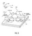
- FIG. 5is an illustration of a portion of an integrated circuit which includes an n type field effect transistor and a p type field effect transistor with a non parallel orientation on a substrate.
- Embodiments of the present inventiondescribe semiconductor structures and methods of forming semiconductor structures.
- numerous specific detailsare set forth in order to provide a thorough understanding of the present invention.
- well known semiconductor processes and manufacturing techniqueshave not been described in particular detail in order to not unnecessarily obscure the present invention.
- the present inventionutilizes atomic layer control of single crystalline semiconductor structures to maximize performance of semiconductor devices.
- hard mask covered single crystalline structuresare exposed to anisotropic wet etches.
- the wet etchhas sufficient chemical strength to overcome the activation energy barrier of the chemical etching reaction in order to etch less dense planes of the semiconductor structure, but insufficient chemical strength to overcome the activation energy barrier of the chemical etching reaction, thereby not etching high density planes.
- natural facets in epitaxial siliconare exploited to negate edge roughness in three-dimensional silicon channel structures.
- natural facetsare exploited to form a three-dimensional channel structure which enables good gate control of the channel region.
- semiconductor bodies of PMOS and NMOS transistorsare formed with specific arrangement on single crystalline semiconductors to exploit the crystal orientation and achieve increased mobility for both holes and electrons.
- FIGS. 2A-2FA method of forming a three-dimensional semiconductor structure utilizing a self limiting etch and natural faceting is illustrated in FIGS. 2A-2F in accordance with embodiments of the present invention.
- the fabrication of a semiconductor structurebegins with a substrate 200 .
- substrate 200is a silicon on insulator (SOI) substrate.
- SOI substrate 200includes a lower monocrystalline silicon substrate 202 .
- An insulating layer 204such as silicon dioxide or silicon nitride, is formed on monocrystalline substrate 202 .
- a single crystalline silicon film 206is formed on the top of the insulating layer 204 .
- Insulating layer 204is sometimes referred to as a “buried oxide” or a “buried insulating” layer and is formed to a thickness sufficient to isolate single crystalline silicon film 206 from lower monocrystalline silicon substrate 202 .
- the insulating layeris a buried oxide layer formed to a thickness between 200-2000 ⁇ .
- the silicon film 206is an intrinsic (i.e., undoped) silicon epitaxial film.
- the single crystalline silicon film 206is doped to a p type or n type conductivity with a concentration level between 1 ⁇ 10 16 -1 ⁇ 10 19 atom/cm 3 .
- Silicon film 206can be in situ doped (i.e., doped while it is deposited) or doped after it is formed on insulating layer 204 by, for example, ion implantation. Doping silicon film 206 after it is deposited enables both n type devices and p type devices to be fabricated on the same substrate. In an embodiment of the present invention, silicon film 206 is formed to a thickness which is approximately equal to the height desired of the subsequently formed silicon structure. In an embodiment of the present invention, the single crystalline silicon film 206 has a thickness of less than 30 nanometers and ideally around 20 nanometers or less.
- a silicon on insulator (SOI) substrate 200can be formed in any well known method.
- SIMOXoxygen atoms are implanted at a high dose into a single crystalline silicon substrate and then annealed to form buried oxide 204 within the substrate. The portion of the single crystalline silicon substrate above the buried oxide becomes the silicon film 206 .
- Another technique currently used to form SOI substratesis an epitaxial silicon film transfer technique which is generally referred to as “bonded SOI”. In this technique, a first silicon wafer has a thin oxide grown on its surface that will later serve as the buried oxide 204 in the SOI structure.
- a high dose hydrogen implantis made into the first silicon wafer to form a stress region below the silicon surface of the first wafer.
- the first waferis then flipped over and bonded to the surface of a second silicon wafer.
- the first waferis then cleaved along the high stress plane created by the hydrogen implant.
- the cleavingresults in a SOI structure with a thin silicon layer on top, the buried oxide underneath, all on top of the second single crystalline silicon wafer.
- Well known smoothing techniquessuch as HCl smoothing or chemical mechanical polishing (CMP) can be used to smooth the top surface of the silicon film 206 to its desired thickness.
- the present inventionwill be described with respect to silicon structures formed on silicon on insulator (SOI) substrates, the present invention can be carried out on standard monocrystalline silicon wafers or substrates to form a “bulk” device.
- the silicon structurescan be formed directly from the monocrystalline silicon wafer or formed from epitaxial silicon films formed on a monocrystalline silicon substrate.
- germaniumgermanium
- Si x Ge ysilicon germanium alloy
- GaAsgallium arsenide
- InSbindium antimonide
- GaPgallium phosphide
- GaSbgallium antimonide
- embodiments of the present inventioninclude semiconductor structures and methods of forming semiconductor structures utilizing semiconductors, such as but not limited to germanium (Ge), a silicon germanium alloy (Si x Ge y ), gallium arsenide (GaAs), indium antimonide (InSb), gallium phosphide (GaP), and gallium antimonide (GaSb).
- semiconductorssuch as but not limited to germanium (Ge), a silicon germanium alloy (Si x Ge y ), gallium arsenide (GaAs), indium antimonide (InSb), gallium phosphide (GaP), and gallium antimonide (GaSb).
- single crystalline silicon film 206has a (100) global crystal orientation, as defined by the xy plane.
- a silicon film with a (100) global crystal orientationhas a ⁇ 100> plane which is planar with the surface of the film. That is, as illustrated in FIG. 2A , a single crystalline silicon film with a (100) global crystal orientation has a ⁇ 100> plane which lies in the xy plane with a normal axis in the z direction.
- brackets ( )are used to illustrate the global crystal orientation of the film, as defined by the xy plane and along the z direction, while pointed brackets ⁇ > are used to describe specific local planes within said globally defined crystalline film.
- a single crystalline silicon with a (100) crystal orientationhas a pair of ⁇ 110> planes which are perpendicular to one another. That is, the (100) single crystalline silicon has a ⁇ 110> plane which lies in the zx plane with a normal axis extending in the y direction and has a ⁇ 110> plane which lies in the zy plane and with a normal axis in the x direction.
- silicon film 206 with a (100) global crystal orientationis etched to form a silicon structure which has a pair of laterally opposite sidewalls which are formed from the ⁇ 110> plane and a second pair of laterally opposite sidewalls, perpendicular thereto, which lie in the ⁇ 110> plane.
- a hard mask material 208can be formed on the top surface 219 of silicon film 206 .
- Hard mask material 208is a material which can provide a hard mask for etching of silicon film 206 .
- Hard mask material 208is a material which can retain its profile during the etching of silicon film 206 .
- Hard mask material 208is a material which will not etch or will only slightly etch during the etching of silicon film 206 .
- the hard mask materialis formed of a material such that the etchant used to etch silicon film 206 will etch silicon film 206 at least 5 times faster than the hard mask material and ideally at least 10 times faster.
- the silicon film and the hard maskare chosen to provide an etch selectivity of at least 5:1 and ideally at least 10:1.
- hard mask material 208is formed from silicon nitride or silicon oxynitride.
- hard mask material 208is formed from a silicon nitride film with between 0-5% carbon, formed by a low pressure chemical vapor deposition (LPCVD) process.
- LPCVDlow pressure chemical vapor deposition
- Hard mask material 208is formed to a thickness sufficient to retain its profile during the entire etch of silicon film 206 but not too thick to cause difficulties in patterning.
- the hard mask material 208is formed to a thickness between 3 nanometers to 50 nanometers and ideally to a thickness around 10 nanometers.
- Photoresist mask 210is formed on hard mask material 208 .
- Photoresist mask 210contains the feature pattern to be transferred into silicon film 206 .
- Photoresist mask 210can be formed by any well known technique, such as by blanket depositing photoresist material and then masking, exposing and developing the photoresist material into a photoresist mask 210 having the desired pattern for a silicon film 206 .
- Photoresist mask 210is typically formed of an organic compound.
- Photoresist mask 210is formed to a thickness sufficient to retain its profile while patterning hard mask film 208 but yet is not formed too thick to prevent its lithographic patterning into the smallest dimensions (i.e., critical dimensions) possible with the photolithography system and process used.
- photoresist mask 210is orientated on single crystalline silicon film 206 so as to define a photoresist mask with a pair of laterally opposite sidewalls aligned with a ⁇ 110> crystal plane and a second pair of laterally opposite sidewalls, perpendicular to the first, aligned with the ⁇ 110> plane.
- hard mask material 208is etched in alignment with photoresist mask 210 to form a hard mask 212 as shown in FIG. 2C .
- Photoresist mask 210prevents the underlying portion of hard mask material 208 from being etched.
- the hard mask material 208is etched with an etchant which can etch the hard mask material but does not etch the underlying silicon film 206 .
- the hard mask materialis etched with an etchant that has almost perfect selectivity to the underlying silicon film 206 .
- the hard mask etchantetches the hard mask material 208 at least 20 times faster than the underlying silicon film 206 (i.e., etchant has a hard mask to silicon film selectivity of at least 20:1).
- hard mask material 208is a silicon nitride or silicon oxynitride film
- hard mask material 208can be etched into a hard mask 212 utilizing a dry etch process, such as a reactive ion etching.
- a silicon nitride or silicon oxynitride hard maskis reactively ion etched utilizing a chemistry comprising CHF 3 and O 2 and Ar.
- photoresist mask 210may be removed by well known techniques. For example, photoresist mask 210 may be removed utilizing “piranha” clean solution which includes sulfuric acid and hydrogen peroxide. Additionally, residue from the photoresist mask 210 may be removed with an O 2 ashing.
- photoresist mask 210prior to patterning silicon film 206 so that a polymer film from the photoresist does not form on the sidewalls of the patterned silicon film 206 .
- silicon film 206is used as a semiconductor body or fin in a nonplanar device, it is desirable to first remove the photoresist mask prior to etching the silicon film because dry etching processes can erode the photoresist mask and cause polymer films to develop on the sidewalls of the silicon body which can be hard to remove and which can detrimentally affect device performance.
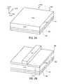
- silicon film 206is etched in alignment with hard mask 212 to form a patterned silicon film 214 which has a first pair of laterally opposite sidewalls 218 aligned with the ⁇ 110> crystal plane and a second pair of laterally opposite sidewalls 220 aligned with the ⁇ 110> crystal plane.
- Hard mask 212prevents the underlying portion of silicon film 206 from being etched during the etch process. In an embodiment of the present invention, the etch is continued until the underlying buried oxide layer 204 is reached. Silicon film 206 is etched with an etchant which etches silicon film 206 without significantly etching hard mask 212 .
- silicon film 206is etched with an etchant which enables silicon film 206 to be etched at least 5 times and ideally 10 times faster than hard mask 212 (i.e., etchant has a silicon film 206 to hard mask 212 etch selectivity of at least 5:1 and ideally at least 10:1). Silicon film 206 can be etched utilizing any suitable process. In an embodiment of the present invention, silicon film 206 is anisotropically etched so that the silicon body 214 has nearly vertical sidewalls 218 formed in alignment with the sidewalls of hard mask 212 .
- silicon film 206can be etched utilizing a dry etch process, such as a reactive ion etch (RIE) or plasma etch with a chemistry comprising Cl 2 and HBr.
- RIEreactive ion etch
- the sidewalls 218will typically have a line edge roughness 222 of about 2-4 nanometers.
- a surface roughnessis unacceptably large and can detrimentally affect device performance.
- the silicon structure 214is exposed to a wet etch or a “faceting” etch while hard mask 212 is present on structure 214 in order to remove the edge roughness and/or to tailor the shape of the structure to enhance device performance.
- the hard mask 212 capped silicon structure 214is exposed to an anisotropic wet etch.
- the wet etchanthas sufficient chemical strength to overcome the activation energy barrier of the chemical etching reaction in order to etch less dense planes of the semiconductor structure, but insufficient chemical strength to overcome the activation energy barrier of the chemical etching reaction, thereby not etching high density planes.
- a wet etch chemistry and processare used which can etch the less dense ⁇ 100> and ⁇ 110> planes but which cannot etch the higher density ⁇ 111> planes. Because hard mask 212 covers the less dense ⁇ 100> plane on the top surface of the silicon structure 214 , said less dense plane is protected from etching. Because the less dense plane ⁇ 100> on the top surface is shielded and because the etch does not have a sufficient chemical strength to etch the ⁇ 111> plane, the wet etch stops on the first total intact or contiguous ⁇ 111> plane as shown in FIG. 2E . In this way, the “faceting” or wet etch is self limiting.
- the faceting etch of the present inventioncan be said to be an anisotropic etch because it etches in one direction at one rate while etching in other directions at a second slower rate or not at all. Because the etch process etches the ⁇ 100> and ⁇ 110> planes but not the ⁇ 111> planes, the faceting or wet etch forms a silicon structure 230 having sidewalls 232 defined by the ⁇ 111> plane as shown in FIG. 2E .
- the anisotropic wet etchremoves the surface roughness 222 from sidewalls 218 ( FIG.
- top surface 219 of structure 230has a width (W 1 ) between laterally opposite sidewalls 232 of between 20-30 nm and the bottom surface has a width (W 2 ) between laterally opposite sidewalls of between 10-15 nm.
- the wet etch or “faceting” etchis a hydroxide based etch with a sufficiently low hydroxide concentration and nucleophillicity (i.e. chemical strength) so that there is no etching of the fully intact ⁇ 111> planes.
- structure 214is exposed to a faceting or wet etch which comprises less than 1% ammonia hydroxide (NH 4 OH) by volume.
- structure 214is exposed to a wet etchant comprising between 0.2-1% NH 4 OH by volume at a temperature range between 5-25° C.
- sonic energy at the frequency range between 600-800 kilohertz dissipating between 0.5-3 watts/cm 2is applied to the etch solution during the faceting etch.
- the hard mask capped silicon structureis exposed to the faceting etch for between 15 seconds-5 minutes.
- the faceting or wet etchcan comprise ultra-dilute ( ⁇ 0.1% by volume) aqueous solutions of tetraalkylammonium hydroxides (e.g. tetraethylammonium hydroxide and tetramethylammonium hydroxide at a temperature between 5 and 20° C.).
- tetraalkylammonium hydroxidese.g. tetraethylammonium hydroxide and tetramethylammonium hydroxide at a temperature between 5 and 20° C.
- the fabricated silicon structure 230can be used to fabricate semiconductor devices, such as transistors and capacitors, as well as micro-electrical mechanical systems (MEMS) and opto-electronic devices.
- semiconductor structure 230is used as a semiconductor body or fin for a nonplanar or three-dimensional transistor, such as but not limited to a tri-gate transistor, a dual gate transistor, a FINFET, an omega-FET or a pi-FET.
- silicon structure 230provides a silicon body or fin for a tri-gate transistor 240 illustrated in FIG. 2F .
- hard mask 212is removed from silicon structure 230 .
- a wet etchcomprising phosphoric acid in de-ionized water may be used to remove the hard mask.
- the hard mask etchantcomprises an aqueous solution of between 80-90% phosphoric acid (by volume) heated to a temperature between 150-170° C. and ideally to 160° C.
- the substrateafter removing hard mask 212 , can be cleaned utilizing standard SC 1 and SC 2 cleans. It is desirable to clean the substrate after removal of the hard mask with phosphoric acid because phosphoric acid typically includes many metallic impurities which can affect device performance or reliability. It is to be appreciated that if one desires to form a FINFET or a dual gate device, the hard mask 212 may be left on silicon structure 230 in order to isolate the top surface of the semiconductor structure 230 from control by a subsequently formed gate electrode.
- gate dielectric layer 250is formed on the sidewalls 232 as well as on the top surface of semiconductor body 230 .
- Gate dielectric layer 250can be any well known and suitable gate dielectric layer, such as but not limited to a silicon dioxide or silicon nitride gate dielectric layer. Additionally, gate dielectric layer 250 can be a high-k gate dielectric layer, such as but not limited to hafnium oxide, zirconium oxide, titanium oxide and tantalum oxide. Any well known technique, such as but not limited to chemical vapor deposition and atomic layer deposition may be utilized to form gate dielectric layer 250 .
- a gate electrode 260is formed on gate dielectric layer 250 on the top surface and sidewalls of semiconductor structure 230 as illustrated in FIG. 2F .
- Gate electrode 260is formed perpendicular to sidewalls 232 .
- the gate electrodecan be formed from any well known gate electrode material, such as but not limited to doped polycrystalline silicon, as well as metal films, such as but not limited to tungsten, tantalum, titanium, and their nitrides. Additionally, it is to be appreciated that a gate electrode need not necessarily be a single material and can be a composite stack of thin films, such as but not limited to a lower metal film formed on the gate dielectric layer with a top polycrystalline silicon film.
- the gate dielectric layer and gate electrodemay be formed by blanket depositing or growing the gate dielectric layer over the semiconductor body and then blanket depositing a gate electrode material over the gate dielectric layer.
- the gate dielectric layer and gate electrode materialmay then be patterned with well know photolithography and etching techniques to form gate electrode 260 and gate dielectric layer 250 as illustrated in FIG. 2F .
- the gate dielectric layer and gate electrodemay be formed utilizing a well known replacement gate process.
- a source region 272 and a drain region 274are formed in silicon body 230 on opposite sides of gate electrode 260 as illustrated in FIG. 2F . Any well known and suitable technique, such as solid source diffusion or ion implantation may be used to form source and drain regions.
- the source region 272 and drain region 274are formed to a concentration between 1 ⁇ 10 19 -1 ⁇ 10 21 atoms/cm 3 .
- the fabricated nonplanar transistor 240includes a semiconductor body 230 surrounded by gate dielectric layer 250 and gate electrode 260 as shown in FIG. 2F .
- the portion of the semiconductor body 230 located beneath the gate dielectric and gate electrodeis the channel region of the device.
- the source and drain regionare doped to a first conductivity type (n type or p type) while the channel region is doped to a second opposite conductivity type (p type or n type) or is left undoped.
- a conductive channelis formed by gate electrode 260 in the channel region of silicon body 230 , charges (i.e., holes or electrons) flow between the source and drain region along the ⁇ 110> plane in silicon body 230 .
- device 240is a p type device where the source and drain regions are formed to a p type conductivity and where the carriers are holes. Additionally, by inwardly tapering the sidewalls of silicon body 230 , gate electrode 260 has good control over the channel region of body 230 enabling fast turn “on” and turn “off” of transistor 240 .
- FIGS. 3A-3Dillustrate a method of forming a monocrystalline silicon body or structure in accordance with another embodiment of the present invention.
- a hard mask 312is formed on a single crystalline silicon film 306 having a (100) global crystal orientation.
- Hard mask 312can be formed as described above.
- the hard mask 312is orientated on silicon film 306 to produce a pair of sidewalls which are aligned with the ⁇ 100> plane and a second pair of sidewalls which are also aligned to the ⁇ 100> plane. (It is to be appreciated that the orientation of hard mask 312 is rotated approximately 45° in the xy plane from the orientation of hard mask 212 in FIG. 2A .)
- the (100) global crystal orientation silicon film 306is etched in alignment with the hard mask 312 to produce a silicon structure 314 which has a pair of laterally opposite sidewalls 318 which are aligned with the ⁇ 100> plane and a second pair of sidewalls 320 , which are perpendicular to the first pair and which are also aligned with the ⁇ 100> plane.
- Silicon film 306can be etched as described above.
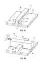
- the silicon structure 314is exposed to a faceting wet etch while hard mask 312 is present on the top surface 319 of silicon structure 314 .
- the faceting wet etchhas a sufficient chemical strength to etch the less dense ⁇ 110> and ⁇ 100> planes but insufficient strength to etch the high density ⁇ 111> plane. Because the less dense ⁇ 100> plane on the top surface 319 of the silicon structure 314 is covered by the hard mask 312 and because the etch does not have sufficient chemical strength to etch the ⁇ 111> plane, the silicon structure 314 is transformed into a silicon structure 330 having a pair of sidewalls 332 having a “V” notched shape formed by intersecting ⁇ 111> planes as illustrated in FIG. 3C .
- the faceting etchis self limiting, and stops at the first contiguous ⁇ 111> planes.
- the ⁇ 111> planes of sidewalls 332meet at an angle ⁇ of approximate 55°.
- a combination of crystal orientation, atom shielding, and a well-controlled anisotropic wet etchenables the formation of silicon structure 330 with “V” notch sidewalls 332 .
- the silicon structure 330can be used to create silicon nonplanar or three-dimensional devices as well as micro-machines and MEMS devices.
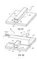
- the silicon structure 330is used to form a nonplanar transistor, such as a tri-gate transistor 330 as illustrated in FIG. 3D .
- Gate electrode 360is formed perpendicular to sidewalls 332 as shown in FIG. 3D .
- the nonplanar devicehas a gate dielectric layer 350 and a gate electrode 360 formed over and around a portion of silicon body 330 as illustrated in FIG. 3D .
- a source region 372 and a drain region 374are formed in the silicon body 330 on opposite sides of the gate electrode.
- the charge migration from the source to the drain region in transistor 340is parallel to or in alignment with the ⁇ 100> plane. Because charge migration is along the ⁇ 100> plane, the silicon structure 330 provides good electron mobility and is therefore ideal for use in the fabrication of an n type field effect transistor (NFET) where the carriers are electrons and the source region 372 and drain regions 374 are n type conductivity.
- NFETn type field effect transistor
- FIGS. 4A-4Dillustrates a method of forming a semiconductor body or structure in accordance with another embodiment of the present invention.
- a substrate 400such as a silicon on insulator (SOI) substrate which includes a lower monocrystalline silicon substrate 402 , a buried oxide layer 404 and a single crystalline silicon film 406 is provided.
- SOIsilicon on insulator
- a silicon on insulator substrate 400is ideally used, other well known semiconductor substrates can be used as set forth above.
- single crystalline silicon film 406has a (110) global crystal orientation as shown in FIG. 4A .
- a single crystalline silicon film with a (110) global crystal orientationhas a ⁇ 110> plane of the silicon lattice which is planar to or parallel with the surface of the film. That is, as illustrated in FIG. 4A , a single crystalline silicon film with a (110) global crystal orientation has a ⁇ 110> plane in the xy plane with a normal axis in the z direction. Additionally, a single crystalline silicon film with a (110) global crystal orientation has ⁇ 111> planes and ⁇ 110> planes which are orthogonal to each other and orthogonal to a ⁇ 110> plane.
- a hard mask 412is formed on single crystalline silicon film 406 having a (110) crystal orientation as described above.
- Hard mask 412is orientated on silicon film 406 to produce a pair of sidewalls aligned with ⁇ 110> plane and a second pair of perpendicular sidewalls which are aligned with the ⁇ 111> plane.
- Hard mask 412can be formed of materials and by methods described above.
- the (110) silicon filmis etched in alignment with hard mask 412 to produce a silicon structure 414 which has a pair of laterally opposite sidewalls 418 which are parallel with or aligned with the ⁇ 110> plane and a second pair of sidewalls 420 , which are perpendicular to the first pair 418 which are parallel with or aligned with a ⁇ 111> plane.
- Hard mask 412 capped silicon structure 414is then exposed to a faceting wet etch.
- the faceting wet etchhas sufficient chemical strength to etch the less dense ⁇ 110> plane, but insufficient chemical strength to etch the higher density ⁇ 111> plane.
- structure 414is transformed into structure 430 having a pair of laterally opposite sidewalls 432 defined by ⁇ 111> planes as illustrated in FIG. 4C .
- the sidewalls 432are defined by the ⁇ 111> planes and generate a structure with a v-shape or inwardly tapered sidewalls.
- the sidewalls 432angle inward from the top surface 419 of structure 430 at an angle gamma of approximately 62.5 degrees.
- the top surface 419has a width (W 1 ) between laterally opposite sidewalls 430 of between 20-30 nm and a bottom surface has width (W 2 ) between laterally opposite sidewalls 440 of between 10-15 nm.
- W 1width between laterally opposite sidewalls 430 of between 20-30 nm
- W 2width between laterally opposite sidewalls 440 of between 10-15 nm.
- structure 430can be used to create a variety of well known semiconductor devices, such as silicon nonplanar or three-dimensional devices, as well as opto-electronic devices and MEMS devices.
- the silicon structure 430is used to form a silicon body of nonplanar transistor, such as a tri-gate transistor 440 , as illustrated in FIG. 4D .
- the tri-gate transistor 440has a gate dielectric layer 450 and a gate electrode 460 formed over and around a portion of silicon body 430 as illustrated in FIG. 4D .
- the gate electrode 460runs in a direction perpendicular to sidewalls 432 as shown in FIG. 4D .
- the gate dielectric layer 450 and gate electrode 460may be formed of any suitable material and suitable known method, such as described above.
- a source region 472 and a drain 474are formed in silicon body 430 on opposite sides of gate electrode 460 as illustrated in FIG. 4D .
- the charge migration from the source region 472 to the drain region 474 in silicon body 430is parallel to or in alignment with the ⁇ 110> plane.
- the inwardly tapered sidewalls 432 of silicon body 430provide good gate control 460 of the channel region of the device which enables the fast turn “on” and turn “off” of device 440 .
- germaniumgermanium
- Si x Ge ysilicon germanium alloy
- GaAsgallium arsenide
- InSbindium antimonide
- GaPgallium phosphide
- GaSbgallium antimonide
- a single crystalline indium antimonide (InSb) structurecan be faceted utilizing a wet etchant comprising an aqueous solution of 0.05-0.1 mol/L citric acid at a temperature range between 5-15° C.
- a single crystalline gallium arsenide (GaAs) structurecan be faceted by exposing a hard mask covered gallium arsenide structure to a wet etchant comprising an aqueous solution of less than 0.05 mol/L citric acid at a temperature range between 5-15° C.
- an integrated circuitis formed from a p type transistor and an n type transistor 520 which are orientated and/or shaped to optimize the performance of each type of transistor.
- a single crystalline silicon film having a (100) global crystal orientationis patterned as described with respect to FIGS. 2A-2F to form a silicon body 512 for a p type nonplanar transistor 510 wherein the charge (hole) migration is parallel with a ⁇ 110> plane and is also patterned as described with respect to FIGS.
- a p type nonplanar transistor and an n type nonplanar transistorare orientated in a non-parallel (e.g., 45° C. offset) manner with respect to one another on a substrate in order to optimize the hole mobility for the p type transistor and the electron mobility for the n type transistor.
- the semiconductor bodies of the p type device and the n type deviceare oriented with respect to one another to enable the faceting etch to shape the bodies into structures which optimize performance for each device type. In this way, the performance of an integrated circuit which includes both an n type nonplanar transistor and a p type nonplanar transistor can be greatly improved.
Landscapes
- Engineering & Computer Science (AREA)
- Microelectronics & Electronic Packaging (AREA)
- Condensed Matter Physics & Semiconductors (AREA)
- General Physics & Mathematics (AREA)
- Manufacturing & Machinery (AREA)
- Computer Hardware Design (AREA)
- Physics & Mathematics (AREA)
- Power Engineering (AREA)
- Chemical & Material Sciences (AREA)
- Chemical Kinetics & Catalysis (AREA)
- General Chemical & Material Sciences (AREA)
- Thin Film Transistor (AREA)
- Crystallography & Structural Chemistry (AREA)
- Internal Circuitry In Semiconductor Integrated Circuit Devices (AREA)
- Weting (AREA)
Abstract
Description
- This application is a divisional of U.S. patent application Ser. No. 11/158,661, filed Jun. 21, 2005, the entire contents of which are hereby incorporated by reference herein.
- 1. Field of the Invention
- The present invention relates to the field of semiconductor processing and more particularly to semiconductor structures and their methods of fabrication.
- 2. Discussion of Related Art
- In order to increase the performance of modern integrated circuits, such as microprocessors, silicon on insulator (SOI) transistors have been proposed. Silicon on insulator (SOI) transistors have an advantage in that they can be operated in a fully depleted manner. Fully depleted transistors have an advantage of ideal subthreshold gradients for optimized on current/off current ratios. An example of a proposed SOI transistor which can be operated in a fully depleted manner is that of a tri-gate
transistor 100, such as illustrated inFIG. 1 .Tri-gate transistor 100 includes asilicon body 104 formed oninsulating substrate 102 having buriedoxide layer 103 formed on amonocrystalline silicon substrate 105. A gatedielectric layer 106 is formed on the top and sidewalls of thesilicon body 104 as shown inFIG. 1 . Agate electrode 108 is formed on the gate dielectric layer and surrounds thebody 104 on three sides essentially providing atransistor 100 having three gate electrodes (G1, G2, G3) one on each of the sidewalls of thesilicon body 104 and one on the top surface of thesilicon body 104. Asource region 110 and adrain region 112 are formed insilicon body 104 on opposite sides ofgate electrode 108 as shown inFIG. 1 . The active channel region is the region of the silicon body located beneathgate electrode 108 and between thesource region 110 anddrain region 112. An advantage of a tri-gatetransistor 100 is that it exhibits good short channel effects (SCEs). One reason tri-gatetransistors 100 exhibit good short channel effects is that the nonplanarity of such devices places thegate electrode 108 in such a way as to surround the active channel region on all three sides. FIG. 1 illustrates a nonplanar or tri-gate transistor.FIGS. 2A-2E illustrate a method of forming a semiconductor structure in accordance with embodiments of the present invention.FIG. 2F is an illustration of a nonplanar transistor formed from the structure ofFIG. 2E .FIGS. 3A-3C illustrate a method of forming a semiconductor structure in accordance with embodiments of the present invention.FIG. 3D is an illustration of a nonplanar transistor utilizing a semiconductor structure ofFIG. 3C .FIGS. 4A-4C illustrate a method of forming a semiconductor structure in accordance with embodiments of the present invention.FIG. 4D is an illustration of a nonplanar transistor utilizing the semiconductor structure ofFIG. 4C .FIG. 5 is an illustration of a portion of an integrated circuit which includes an n type field effect transistor and a p type field effect transistor with a non parallel orientation on a substrate.- Embodiments of the present invention describe semiconductor structures and methods of forming semiconductor structures. In the following description numerous specific details are set forth in order to provide a thorough understanding of the present invention. In other instances, well known semiconductor processes and manufacturing techniques have not been described in particular detail in order to not unnecessarily obscure the present invention.
- The present invention utilizes atomic layer control of single crystalline semiconductor structures to maximize performance of semiconductor devices. In embodiments of the present invention, hard mask covered single crystalline structures are exposed to anisotropic wet etches. The wet etch has sufficient chemical strength to overcome the activation energy barrier of the chemical etching reaction in order to etch less dense planes of the semiconductor structure, but insufficient chemical strength to overcome the activation energy barrier of the chemical etching reaction, thereby not etching high density planes. By choosing proper crystal orientation and by forming a hard mask over the less dense planes of the structure and by using a wet etch chemistry with the appropriate chemical strength, one can form semiconductor structures with desired faceting, crystal orientation and sidewall smoothing. In embodiments of the present invention, natural facets in epitaxial silicon are exploited to negate edge roughness in three-dimensional silicon channel structures. In an embodiment of the present invention, natural facets are exploited to form a three-dimensional channel structure which enables good gate control of the channel region. In yet other embodiments of the present invention, semiconductor bodies of PMOS and NMOS transistors are formed with specific arrangement on single crystalline semiconductors to exploit the crystal orientation and achieve increased mobility for both holes and electrons. Other aspects of the present invention will become obvious from the detailed description which follows.
- A method of forming a three-dimensional semiconductor structure utilizing a self limiting etch and natural faceting is illustrated in
FIGS. 2A-2F in accordance with embodiments of the present invention. The fabrication of a semiconductor structure begins with asubstrate 200. In an embodiment of the present invention,substrate 200 is a silicon on insulator (SOI) substrate. ASOI substrate 200 includes a lowermonocrystalline silicon substrate 202. Aninsulating layer 204, such as silicon dioxide or silicon nitride, is formed onmonocrystalline substrate 202. A singlecrystalline silicon film 206 is formed on the top of theinsulating layer 204. Insulatinglayer 204 is sometimes referred to as a “buried oxide” or a “buried insulating” layer and is formed to a thickness sufficient to isolate singlecrystalline silicon film 206 from lowermonocrystalline silicon substrate 202. In an embodiment of the present invention, the insulating layer is a buried oxide layer formed to a thickness between 200-2000 Å. In an embodiment of the present invention, thesilicon film 206 is an intrinsic (i.e., undoped) silicon epitaxial film. In other embodiments, the singlecrystalline silicon film 206 is doped to a p type or n type conductivity with a concentration level between 1×10¹⁶-1×10¹⁹atom/cm3.Silicon film 206 can be in situ doped (i.e., doped while it is deposited) or doped after it is formed on insulatinglayer 204 by, for example, ion implantation.Doping silicon film 206 after it is deposited enables both n type devices and p type devices to be fabricated on the same substrate. In an embodiment of the present invention,silicon film 206 is formed to a thickness which is approximately equal to the height desired of the subsequently formed silicon structure. In an embodiment of the present invention, the singlecrystalline silicon film 206 has a thickness of less than 30 nanometers and ideally around 20 nanometers or less. - A silicon on insulator (SOI)
substrate 200 can be formed in any well known method. In one method of forming the silicon on insulator substrate, known as the SIMOX technique, oxygen atoms are implanted at a high dose into a single crystalline silicon substrate and then annealed to form buriedoxide 204 within the substrate. The portion of the single crystalline silicon substrate above the buried oxide becomes thesilicon film 206. Another technique currently used to form SOI substrates is an epitaxial silicon film transfer technique which is generally referred to as “bonded SOI”. In this technique, a first silicon wafer has a thin oxide grown on its surface that will later serve as the buriedoxide 204 in the SOI structure. Next, a high dose hydrogen implant is made into the first silicon wafer to form a stress region below the silicon surface of the first wafer. The first wafer is then flipped over and bonded to the surface of a second silicon wafer. The first wafer is then cleaved along the high stress plane created by the hydrogen implant. The cleaving results in a SOI structure with a thin silicon layer on top, the buried oxide underneath, all on top of the second single crystalline silicon wafer. Well known smoothing techniques, such as HCl smoothing or chemical mechanical polishing (CMP) can be used to smooth the top surface of thesilicon film 206 to its desired thickness. - Although the present invention will be described with respect to silicon structures formed on silicon on insulator (SOI) substrates, the present invention can be carried out on standard monocrystalline silicon wafers or substrates to form a “bulk” device. The silicon structures can be formed directly from the monocrystalline silicon wafer or formed from epitaxial silicon films formed on a monocrystalline silicon substrate. Additionally, although embodiments of the present invention are illustrated with respect to the formation of single crystalline silicon structures and devices formed therefrom, the methods and structures of the present invention are equally applicable to other types of semiconductors, such as but not limited to germanium (Ge), a silicon germanium alloy (SixGey), gallium arsenide (GaAs), indium antimonide (InSb), gallium phosphide (GaP), and gallium antimonide (GaSb). Accordingly, embodiments of the present invention include semiconductor structures and methods of forming semiconductor structures utilizing semiconductors, such as but not limited to germanium (Ge), a silicon germanium alloy (SixGey), gallium arsenide (GaAs), indium antimonide (InSb), gallium phosphide (GaP), and gallium antimonide (GaSb).
- In
FIG. 2A , singlecrystalline silicon film 206 has a (100) global crystal orientation, as defined by thexy plane. A silicon film with a (100) global crystal orientation has a <100> plane which is planar with the surface of the film. That is, as illustrated inFIG. 2A , a single crystalline silicon film with a (100) global crystal orientation has a <100> plane which lies in thexy plane with a normal axis in the z direction. - In the following description round brackets ( ) are used to illustrate the global crystal orientation of the film, as defined by the
xy plane and along the z direction, while pointed brackets < > are used to describe specific local planes within said globally defined crystalline film. - Additionally, as illustrated in
FIG. 2A , a single crystalline silicon with a (100) crystal orientation has a pair of <110> planes which are perpendicular to one another. That is, the (100) single crystalline silicon has a <110> plane which lies in thezx plane with a normal axis extending in the y direction and has a <110> plane which lies in thezy plane and with a normal axis in the x direction. In an embodiment of the present invention,silicon film 206 with a (100) global crystal orientation is etched to form a silicon structure which has a pair of laterally opposite sidewalls which are formed from the <110> plane and a second pair of laterally opposite sidewalls, perpendicular thereto, which lie in the <110> plane. - In order to etch
silicon film 206 into a silicon body, ahard mask material 208 can be formed on thetop surface 219 ofsilicon film 206.Hard mask material 208 is a material which can provide a hard mask for etching ofsilicon film 206.Hard mask material 208 is a material which can retain its profile during the etching ofsilicon film 206.Hard mask material 208 is a material which will not etch or will only slightly etch during the etching ofsilicon film 206. In an embodiment of the present invention, the hard mask material is formed of a material such that the etchant used to etchsilicon film 206 will etchsilicon film 206 at least 5 times faster than the hard mask material and ideally at least 10 times faster. That is, in an embodiment of the present invention, the silicon film and the hard mask are chosen to provide an etch selectivity of at least 5:1 and ideally at least 10:1. In an embodiment of the present invention,hard mask material 208 is formed from silicon nitride or silicon oxynitride. In an embodiment of the present invention,hard mask material 208 is formed from a silicon nitride film with between 0-5% carbon, formed by a low pressure chemical vapor deposition (LPCVD) process.Hard mask material 208 is formed to a thickness sufficient to retain its profile during the entire etch ofsilicon film 206 but not too thick to cause difficulties in patterning. In an embodiment of the present invention, thehard mask material 208 is formed to a thickness between 3 nanometers to 50 nanometers and ideally to a thickness around 10 nanometers. - Next, as also shown in
FIG. 2B , aphotoresist mask 210 is formed onhard mask material 208.Photoresist mask 210 contains the feature pattern to be transferred intosilicon film 206.Photoresist mask 210 can be formed by any well known technique, such as by blanket depositing photoresist material and then masking, exposing and developing the photoresist material into aphotoresist mask 210 having the desired pattern for asilicon film 206.Photoresist mask 210 is typically formed of an organic compound.Photoresist mask 210 is formed to a thickness sufficient to retain its profile while patterninghard mask film 208 but yet is not formed too thick to prevent its lithographic patterning into the smallest dimensions (i.e., critical dimensions) possible with the photolithography system and process used. In an embodiment of the present invention,photoresist mask 210 is orientated on singlecrystalline silicon film 206 so as to define a photoresist mask with a pair of laterally opposite sidewalls aligned with a <110> crystal plane and a second pair of laterally opposite sidewalls, perpendicular to the first, aligned with the <110> plane. - Next, as shown in
FIG. 2C ,hard mask material 208 is etched in alignment withphotoresist mask 210 to form ahard mask 212 as shown inFIG. 2C .Photoresist mask 210 prevents the underlying portion ofhard mask material 208 from being etched. In an embodiment of the present invention, thehard mask material 208 is etched with an etchant which can etch the hard mask material but does not etch theunderlying silicon film 206. In an embodiment of the present invention, the hard mask material is etched with an etchant that has almost perfect selectivity to theunderlying silicon film 206. That is, in an embodiment of the present invention, the hard mask etchant etches thehard mask material 208 at least 20 times faster than the underlying silicon film206 (i.e., etchant has a hard mask to silicon film selectivity of at least 20:1). Whenhard mask material 208 is a silicon nitride or silicon oxynitride film,hard mask material 208 can be etched into ahard mask 212 utilizing a dry etch process, such as a reactive ion etching. In an embodiment of the present invention, a silicon nitride or silicon oxynitride hard mask is reactively ion etched utilizing a chemistry comprising CHF3and O2and Ar. - Next, as also shown in
FIG. 2C , afterhard mask film 208 has been patterned into ahard mask 212,photoresist mask 210 may be removed by well known techniques. For example,photoresist mask 210 may be removed utilizing “piranha” clean solution which includes sulfuric acid and hydrogen peroxide. Additionally, residue from thephotoresist mask 210 may be removed with an O2ashing. - Although not required, it is desirable to remove
photoresist mask 210 prior topatterning silicon film 206 so that a polymer film from the photoresist does not form on the sidewalls of the patternedsilicon film 206. For example, whensilicon film 206 is used as a semiconductor body or fin in a nonplanar device, it is desirable to first remove the photoresist mask prior to etching the silicon film because dry etching processes can erode the photoresist mask and cause polymer films to develop on the sidewalls of the silicon body which can be hard to remove and which can detrimentally affect device performance. - Next, as shown in
FIG. 2D ,silicon film 206 is etched in alignment withhard mask 212 to form a patternedsilicon film 214 which has a first pair of laterallyopposite sidewalls 218 aligned with the <110> crystal plane and a second pair of laterallyopposite sidewalls 220 aligned with the <110> crystal plane.Hard mask 212 prevents the underlying portion ofsilicon film 206 from being etched during the etch process. In an embodiment of the present invention, the etch is continued until the underlying buriedoxide layer 204 is reached.Silicon film 206 is etched with an etchant which etchessilicon film 206 without significantly etchinghard mask 212. In an embodiment of the present invention,silicon film 206 is etched with an etchant which enablessilicon film 206 to be etched at least 5 times and ideally 10 times faster than hard mask212 (i.e., etchant has asilicon film 206 tohard mask 212 etch selectivity of at least 5:1 and ideally at least 10:1).Silicon film 206 can be etched utilizing any suitable process. In an embodiment of the present invention,silicon film 206 is anisotropically etched so that thesilicon body 214 has nearlyvertical sidewalls 218 formed in alignment with the sidewalls ofhard mask 212. Whenhard mask 212 is a silicon nitride or silicon oxynitride film,silicon film 206 can be etched utilizing a dry etch process, such as a reactive ion etch (RIE) or plasma etch with a chemistry comprising Cl2and HBr. - After etching
silicon film 206 to form silicon body orstructure 214, thesidewalls 218 will typically have aline edge roughness 222 of about 2-4 nanometers. When forming a silicon body or structure with a width betweensidewalls 218 of only 20-30 nanometers, such a surface roughness is unacceptably large and can detrimentally affect device performance. - Accordingly, in an embodiment of the present invention, the
silicon structure 214 is exposed to a wet etch or a “faceting” etch whilehard mask 212 is present onstructure 214 in order to remove the edge roughness and/or to tailor the shape of the structure to enhance device performance. In an embodiment of the present invention, thehard mask 212 cappedsilicon structure 214, is exposed to an anisotropic wet etch. The wet etchant has sufficient chemical strength to overcome the activation energy barrier of the chemical etching reaction in order to etch less dense planes of the semiconductor structure, but insufficient chemical strength to overcome the activation energy barrier of the chemical etching reaction, thereby not etching high density planes. - In an embodiment of the present invention, a wet etch chemistry and process are used which can etch the less dense <100> and <110> planes but which cannot etch the higher density <111> planes. Because
hard mask 212 covers the less dense <100> plane on the top surface of thesilicon structure 214, said less dense plane is protected from etching. Because the less dense plane <100> on the top surface is shielded and because the etch does not have a sufficient chemical strength to etch the <111> plane, the wet etch stops on the first total intact or contiguous <111> plane as shown inFIG. 2E . In this way, the “faceting” or wet etch is self limiting. Thus, upon self-limitation of the wet etch, only <111> planes and etch-resistant films used to shield the less dense <110> and <100> planes remain exposed. The faceting etch of the present invention can be said to be an anisotropic etch because it etches in one direction at one rate while etching in other directions at a second slower rate or not at all. Because the etch process etches the <100> and <110> planes but not the <111> planes, the faceting or wet etch forms asilicon structure 230 havingsidewalls 232 defined by the <111> plane as shown inFIG. 2E . The anisotropic wet etch removes thesurface roughness 222 from sidewalls218 (FIG. 2D ) and generates opticallysmooth sidewalls 232 as shown inFIG. 2E . Additionally, after exposing thestructure 214 to the faceting etch for a sufficient period of time, sidewalls218 are defined by the <111> plane and generate astructure 230 with a v-shape or inwardly taperedsidewalls 232. Thesidewalls 232 angle inward from thetop surface 219 ofstructure 230 at an angle alfa of 62.5 degrees. In an embodiment of the present invention, thetop surface 219 ofstructure 230 has a width (W1) between laterallyopposite sidewalls 232 of between 20-30 nm and the bottom surface has a width (W2) between laterally opposite sidewalls of between 10-15 nm. - In an embodiment of the present invention, the wet etch or “faceting” etch is a hydroxide based etch with a sufficiently low hydroxide concentration and nucleophillicity (i.e. chemical strength) so that there is no etching of the fully intact <111> planes. In an embodiment of the present invention,
structure 214 is exposed to a faceting or wet etch which comprises less than 1% ammonia hydroxide (NH4OH) by volume. In an embodiment of the present invention,structure 214 is exposed to a wet etchant comprising between 0.2-1% NH4OH by volume at a temperature range between 5-25° C. In an embodiment of the present invention, sonic energy at the frequency range between 600-800 kilohertz dissipating between 0.5-3 watts/cm2is applied to the etch solution during the faceting etch. In an embodiment of the present invention, the hard mask capped silicon structure is exposed to the faceting etch for between 15 seconds-5 minutes. - In another embodiment of the present invention, the faceting or wet etch can comprise ultra-dilute (<0.1% by volume) aqueous solutions of tetraalkylammonium hydroxides (e.g. tetraethylammonium hydroxide and tetramethylammonium hydroxide at a temperature between 5 and 20° C.).
- The fabricated
silicon structure 230 can be used to fabricate semiconductor devices, such as transistors and capacitors, as well as micro-electrical mechanical systems (MEMS) and opto-electronic devices. In an embodiment of the present invention,semiconductor structure 230 is used as a semiconductor body or fin for a nonplanar or three-dimensional transistor, such as but not limited to a tri-gate transistor, a dual gate transistor, a FINFET, an omega-FET or a pi-FET. - In an embodiment of the present invention,
silicon structure 230 provides a silicon body or fin for atri-gate transistor 240 illustrated inFIG. 2F . In order to fabricate atri-gate transistor 240 as illustrated inFIG. 2F ,hard mask 212 is removed fromsilicon structure 230. In an embodiment of the present invention, whenhard mask 212 is a silicon nitride or silicon oxynitride film, a wet etch comprising phosphoric acid in de-ionized water may be used to remove the hard mask. In an embodiment of the present invention, the hard mask etchant comprises an aqueous solution of between 80-90% phosphoric acid (by volume) heated to a temperature between 150-170° C. and ideally to 160° C. In an embodiment of the present invention, after removinghard mask 212, the substrate can be cleaned utilizing standard SC1 and SC2 cleans. It is desirable to clean the substrate after removal of the hard mask with phosphoric acid because phosphoric acid typically includes many metallic impurities which can affect device performance or reliability. It is to be appreciated that if one desires to form a FINFET or a dual gate device, thehard mask 212 may be left onsilicon structure 230 in order to isolate the top surface of thesemiconductor structure 230 from control by a subsequently formed gate electrode. - Next, a
gate dielectric layer 250 is formed on thesidewalls 232 as well as on the top surface ofsemiconductor body 230.Gate dielectric layer 250 can be any well known and suitable gate dielectric layer, such as but not limited to a silicon dioxide or silicon nitride gate dielectric layer. Additionally,gate dielectric layer 250 can be a high-k gate dielectric layer, such as but not limited to hafnium oxide, zirconium oxide, titanium oxide and tantalum oxide. Any well known technique, such as but not limited to chemical vapor deposition and atomic layer deposition may be utilized to formgate dielectric layer 250. - Next, a
gate electrode 260 is formed ongate dielectric layer 250 on the top surface and sidewalls ofsemiconductor structure 230 as illustrated inFIG. 2F .Gate electrode 260 is formed perpendicular to sidewalls232. The gate electrode can be formed from any well known gate electrode material, such as but not limited to doped polycrystalline silicon, as well as metal films, such as but not limited to tungsten, tantalum, titanium, and their nitrides. Additionally, it is to be appreciated that a gate electrode need not necessarily be a single material and can be a composite stack of thin films, such as but not limited to a lower metal film formed on the gate dielectric layer with a top polycrystalline silicon film. The gate dielectric layer and gate electrode may be formed by blanket depositing or growing the gate dielectric layer over the semiconductor body and then blanket depositing a gate electrode material over the gate dielectric layer. The gate dielectric layer and gate electrode material may then be patterned with well know photolithography and etching techniques to formgate electrode 260 andgate dielectric layer 250 as illustrated inFIG. 2F . Alternatively, the gate dielectric layer and gate electrode may be formed utilizing a well known replacement gate process. Asource region 272 and adrain region 274 are formed insilicon body 230 on opposite sides ofgate electrode 260 as illustrated inFIG. 2F . Any well known and suitable technique, such as solid source diffusion or ion implantation may be used to form source and drain regions. In an embodiment of the present invention, thesource region 272 and drainregion 274 are formed to a concentration between 1×10¹⁹-1×10²¹atoms/cm3. - The fabricated
nonplanar transistor 240 includes asemiconductor body 230 surrounded bygate dielectric layer 250 andgate electrode 260 as shown inFIG. 2F . The portion of thesemiconductor body 230 located beneath the gate dielectric and gate electrode is the channel region of the device. In an embodiment of the present invention the source and drain region are doped to a first conductivity type (n type or p type) while the channel region is doped to a second opposite conductivity type (p type or n type) or is left undoped. When a conductive channel is formed bygate electrode 260 in the channel region ofsilicon body 230, charges (i.e., holes or electrons) flow between the source and drain region along the <110> plane insilicon body 230. That is, intransistor 240, charge migration is along the <110> crystal plane instructure 240. Is has been found that charge migration in the <110> direction provides good hole mobility. Accordingly, in an embodiment of the present invention,device 240 is a p type device where the source and drain regions are formed to a p type conductivity and where the carriers are holes. Additionally, by inwardly tapering the sidewalls ofsilicon body 230,gate electrode 260 has good control over the channel region ofbody 230 enabling fast turn “on” and turn “off” oftransistor 240. FIGS. 3A-3D illustrate a method of forming a monocrystalline silicon body or structure in accordance with another embodiment of the present invention. As shown inFIG. 3A , ahard mask 312 is formed on a singlecrystalline silicon film 306 having a (100) global crystal orientation.Hard mask 312 can be formed as described above. InFIG. 3A , however, thehard mask 312 is orientated onsilicon film 306 to produce a pair of sidewalls which are aligned with the <100> plane and a second pair of sidewalls which are also aligned to the <100> plane. (It is to be appreciated that the orientation ofhard mask 312 is rotated approximately 45° in thexy plane from the orientation ofhard mask 212 inFIG. 2A .)- Next, as illustrated in
FIG. 3B , the (100) global crystalorientation silicon film 306 is etched in alignment with thehard mask 312 to produce asilicon structure 314 which has a pair of laterallyopposite sidewalls 318 which are aligned with the <100> plane and a second pair ofsidewalls 320, which are perpendicular to the first pair and which are also aligned with the <100> plane.Silicon film 306 can be etched as described above. - Next, the
silicon structure 314 is exposed to a faceting wet etch whilehard mask 312 is present on thetop surface 319 ofsilicon structure 314. The faceting wet etch has a sufficient chemical strength to etch the less dense <110> and <100> planes but insufficient strength to etch the high density <111> plane. Because the less dense <100> plane on thetop surface 319 of thesilicon structure 314 is covered by thehard mask 312 and because the etch does not have sufficient chemical strength to etch the <111> plane, thesilicon structure 314 is transformed into asilicon structure 330 having a pair ofsidewalls 332 having a “V” notched shape formed by intersecting <111> planes as illustrated inFIG. 3C . As before, the faceting etch is self limiting, and stops at the first contiguous <111> planes. The <111> planes ofsidewalls 332 meet at an angle θ of approximate 55°. A combination of crystal orientation, atom shielding, and a well-controlled anisotropic wet etch enables the formation ofsilicon structure 330 with “V”notch sidewalls 332. - As discussed above, the
silicon structure 330 can be used to create silicon nonplanar or three-dimensional devices as well as micro-machines and MEMS devices. In an embodiment of the present invention, thesilicon structure 330 is used to form a nonplanar transistor, such as atri-gate transistor 330 as illustrated inFIG. 3D .Gate electrode 360 is formed perpendicular to sidewalls332 as shown inFIG. 3D . The nonplanar device has agate dielectric layer 350 and agate electrode 360 formed over and around a portion ofsilicon body 330 as illustrated inFIG. 3D . Asource region 372 and adrain region 374 are formed in thesilicon body 330 on opposite sides of the gate electrode. The charge migration from the source to the drain region intransistor 340 is parallel to or in alignment with the <100> plane. Because charge migration is along the <100> plane, thesilicon structure 330 provides good electron mobility and is therefore ideal for use in the fabrication of an n type field effect transistor (NFET) where the carriers are electrons and thesource region 372 anddrain regions 374 are n type conductivity. FIGS. 4A-4D illustrates a method of forming a semiconductor body or structure in accordance with another embodiment of the present invention. As shown inFIG. 4A , a substrate400, such as a silicon on insulator (SOI) substrate which includes a lowermonocrystalline silicon substrate 402, a buriedoxide layer 404 and a singlecrystalline silicon film 406 is provided. Although, a silicon on insulator substrate400 is ideally used, other well known semiconductor substrates can be used as set forth above. In an embodiment of the present invention, singlecrystalline silicon film 406 has a (110) global crystal orientation as shown inFIG. 4A . A single crystalline silicon film with a (110) global crystal orientation has a <110> plane of the silicon lattice which is planar to or parallel with the surface of the film. That is, as illustrated inFIG. 4A , a single crystalline silicon film with a (110) global crystal orientation has a <110> plane in thexy plane with a normal axis in the z direction. Additionally, a single crystalline silicon film with a (110) global crystal orientation has <111> planes and <110> planes which are orthogonal to each other and orthogonal to a <110> plane. That is, in a singlecrystalline silicon film 406 with (110) global crystal orientation there are <111> planes which lie in thexz plane with normal axis in the y direction and there are <110> planes which lie in thezy plane and have a normal axis in the x direction as shown inFIG. 4A . Next, ahard mask 412, as shown inFIG. 4A , is formed on singlecrystalline silicon film 406 having a (110) crystal orientation as described above.Hard mask 412 is orientated onsilicon film 406 to produce a pair of sidewalls aligned with <110> plane and a second pair of perpendicular sidewalls which are aligned with the <111> plane.Hard mask 412 can be formed of materials and by methods described above.- Next, as illustrated in
FIG. 4B , the (110) silicon film is etched in alignment withhard mask 412 to produce asilicon structure 414 which has a pair of laterallyopposite sidewalls 418 which are parallel with or aligned with the <110> plane and a second pair ofsidewalls 420, which are perpendicular to thefirst pair 418 which are parallel with or aligned with a <111> plane.Hard mask 412 cappedsilicon structure 414 is then exposed to a faceting wet etch. The faceting wet etch has sufficient chemical strength to etch the less dense <110> plane, but insufficient chemical strength to etch the higher density <111> plane. Because the less dense <110> plane of thetop surface 419 is covered byhard mask 412 and because the etch does not have sufficient chemical strength to etch the <111> plane,structure 414 is transformed intostructure 430 having a pair of laterallyopposite sidewalls 432 defined by <111> planes as illustrated inFIG. 4C . After exposingstructure 414 to the faceting etch for a sufficient period of time, thesidewalls 432 are defined by the <111> planes and generate a structure with a v-shape or inwardly tapered sidewalls. Thesidewalls 432 angle inward from thetop surface 419 ofstructure 430 at an angle gamma of approximately 62.5 degrees. In an embodiment of the present invention, thetop surface 419 has a width (W1) between laterallyopposite sidewalls 430 of between 20-30 nm and a bottom surface has width (W2) between laterallyopposite sidewalls 440 of between 10-15 nm. A combination of crystal orientation, hard mask shielding, and a wet etch with the appropriate chemical strength enables the formation ofsilicon structure 430 with inwardly taperedsidewalls 432. - As discussed above,
structure 430 can be used to create a variety of well known semiconductor devices, such as silicon nonplanar or three-dimensional devices, as well as opto-electronic devices and MEMS devices. In an embodiment of the present invention, thesilicon structure 430 is used to form a silicon body of nonplanar transistor, such as atri-gate transistor 440, as illustrated inFIG. 4D . Thetri-gate transistor 440 has agate dielectric layer 450 and agate electrode 460 formed over and around a portion ofsilicon body 430 as illustrated inFIG. 4D . Thegate electrode 460 runs in a direction perpendicular to sidewalls432 as shown inFIG. 4D . Thegate dielectric layer 450 andgate electrode 460 may be formed of any suitable material and suitable known method, such as described above. Asource region 472 and adrain 474 are formed insilicon body 430 on opposite sides ofgate electrode 460 as illustrated inFIG. 4D . The charge migration from thesource region 472 to thedrain region 474 insilicon body 430 is parallel to or in alignment with the <110> plane. The inwardly taperedsidewalls 432 ofsilicon body 430 providegood gate control 460 of the channel region of the device which enables the fast turn “on” and turn “off” ofdevice 440. - Although the present invention thus far has been described with respect to the shaping or “faceting” of single crystalline silicon structures utilizing a combination of crystal orientation, hard mask shielding, and well controlled wet etchants, concepts of the present invention are equally applicable to other types of single crystalline semiconductor films, such as but not limited to germanium (Ge), a silicon germanium alloy (SixGey), gallium arsenide (GaAs), indium antimonide (InSb), gallium phosphide (GaP), and gallium antimonide (GaSb). For example, a single crystalline indium antimonide (InSb) structure can be faceted utilizing a wet etchant comprising an aqueous solution of 0.05-0.1 mol/L citric acid at a temperature range between 5-15° C. Similarly, a single crystalline gallium arsenide (GaAs) structure can be faceted by exposing a hard mask covered gallium arsenide structure to a wet etchant comprising an aqueous solution of less than 0.05 mol/L citric acid at a temperature range between 5-15° C.
- Additionally, in an embodiment of the present invention, an integrated circuit is formed from a p type transistor and an
n type transistor 520 which are orientated and/or shaped to optimize the performance of each type of transistor. For example, as illustrated inFIG. 5 , in an embodiment of the present invention a single crystalline silicon film having a (100) global crystal orientation is patterned as described with respect toFIGS. 2A-2F to form asilicon body 512 for a ptype nonplanar transistor 510 wherein the charge (hole) migration is parallel with a <110> plane and is also patterned as described with respect toFIGS. 3A-3D to form asilicon body 522 for a ntype nonplanar transistor 520 wherein charge (electron) migration is parallel with a <100> plane. Accordingly, in an embodiment of the present invention, a p type nonplanar transistor and an n type nonplanar transistor are orientated in a non-parallel (e.g., 45° C. offset) manner with respect to one another on a substrate in order to optimize the hole mobility for the p type transistor and the electron mobility for the n type transistor. In other embodiments of the present invention, the semiconductor bodies of the p type device and the n type device are oriented with respect to one another to enable the faceting etch to shape the bodies into structures which optimize performance for each device type. In this way, the performance of an integrated circuit which includes both an n type nonplanar transistor and a p type nonplanar transistor can be greatly improved.
Claims (19)
1. An integrated circuit comprising:
a first nonplanar transistor having a first semiconductor body comprising V-notched sidewalls, wherein charge migration in the first semiconductor body is along a first direction; and
a second nonplanar transistor having a second semiconductor body comprising inwardly tapered sidewalls, wherein charge migration in the second semiconductor body is along a second direction, and wherein the second direction is not parallel to the first direction.
2. The integrated circuit ofclaim 1 , wherein the first direction is approximately 45 degrees with respect to the second direction.
3. The integrated circuit ofclaim 1 , wherein the first nonplanar transistor is an n type field effect transistor, wherein the first semiconductor body is formed from a single crystalline silicon film, and wherein the first direction is parallel to a <100> plane of the single crystalline silicon film.
4. The integrated circuit ofclaim 1 , wherein the second nonplanar transistor is a p type field effect transistor, wherein the second semiconductor body is a single crystalline silicon film, and wherein the second direction is parallel to a <110> plane.
5. The integrated circuit ofclaim 1 , wherein the second nonplanar transistor is a p type field effect transistor, wherein the second semiconductor body is formed from a single crystalline silicon film, wherein the second direction is parallel to a <110> plane of the silicon film, wherein the first nonplanar transistor is an n type field effect transistor, wherein the first semiconductor body is a single crystalline silicon film, and wherein the first direction is parallel to a <100> plane.
6. The integrated circuit ofclaim 1 , wherein the inwardly tapered sidewalls each taper inward from the top of the second semiconductor body at an angle of approximately 62.5 degrees.
7. The integrated circuit ofclaim 6 , wherein each sidewall is flat from the top of the second semiconductor body to the bottom of the second semiconductor body.
8. The integrated circuit ofclaim 1 , wherein the V-notched sidewalls each notch inward from the sides of the first semiconductor body at an angle of approximately 55 degrees.
9. The integrated circuit ofclaim 8 , wherein each sidewall is flat from the top of the first semiconductor body to the center of the V-notch, and is flat from the center of the V-notch to the bottom of the first semiconductor body.
10. The integrated circuit ofclaim 1 , wherein charge migration in the second semiconductor body is along a direction perpendicular to the inwardly tapered sidewalls.
11. The integrated circuit ofclaim 1 , wherein charge migration in the first semiconductor body is along a direction perpendicular to the V-notched sidewalls.
12. A nonplanar transistor, comprising:
a semiconductor body comprising inwardly tapered sidewalls, wherein charge migration in the semiconductor body is along a direction perpendicular to the sidewalls; and
a gate electrode disposed over the semiconductor body and orthogonal to the direction of charge migration.
13. The nonplanar transistor ofclaim 12 , wherein the inwardly tapered sidewalls each taper inward from the top of the semiconductor body at an angle of approximately 62.5 degrees.
14. The nonplanar transistor ofclaim 12 , wherein each sidewall is flat from the top of the semiconductor body to the bottom of the semiconductor body.
15. The nonplanar transistor ofclaim 12 , wherein the nonplanar transistor is a p type field effect transistor, wherein the semiconductor body is formed from a single crystalline silicon film, and wherein the direction perpendicular to the sidewalls is parallel to a <110> plane of the single crystalline silicon film.
16. A nonplanar transistor, comprising:
a semiconductor body comprising V-notched sidewalls, wherein charge migration in the semiconductor body is along a direction perpendicular to the V-notched sidewalls; and
a gate electrode disposed over the semiconductor body and orthogonal to the direction of charge migration.
17. The nonplanar transistor ofclaim 16 , wherein the V-notched sidewalls each notch inward from the sides of the semiconductor body at an angle of approximately 55 degrees.
18. The nonplanar transistor ofclaim 16 , wherein each sidewall is flat from the top of the semiconductor body to the center of the V-notch, and is flat from the center of the V-notch to the bottom of the semiconductor body.
19. The nonplanar transistor ofclaim 16 , wherein the nonplanar transistor is an n type field effect transistor, wherein the semiconductor body is formed from a single crystalline silicon film, and wherein the direction perpendicular to the sidewalls is parallel to a <100> plane of the single crystalline silicon film.
Priority Applications (5)
| Application Number | Priority Date | Filing Date | Title |
|---|---|---|---|
| US12/463,309US8071983B2 (en) | 2005-06-21 | 2009-05-08 | Semiconductor device structures and methods of forming semiconductor structures |
| US13/277,897US8581258B2 (en) | 2005-06-21 | 2011-10-20 | Semiconductor device structures and methods of forming semiconductor structures |
| US14/048,923US8933458B2 (en) | 2005-06-21 | 2013-10-08 | Semiconductor device structures and methods of forming semiconductor structures |
| US14/576,111US9385180B2 (en) | 2005-06-21 | 2014-12-18 | Semiconductor device structures and methods of forming semiconductor structures |
| US15/182,343US9761724B2 (en) | 2005-06-21 | 2016-06-14 | Semiconductor device structures and methods of forming semiconductor structures |
Applications Claiming Priority (2)
| Application Number | Priority Date | Filing Date | Title |
|---|---|---|---|
| US11/158,661US7547637B2 (en) | 2005-06-21 | 2005-06-21 | Methods for patterning a semiconductor film |
| US12/463,309US8071983B2 (en) | 2005-06-21 | 2009-05-08 | Semiconductor device structures and methods of forming semiconductor structures |
Related Parent Applications (1)
| Application Number | Title | Priority Date | Filing Date |
|---|---|---|---|
| US11/158,661DivisionUS7547637B2 (en) | 2005-06-21 | 2005-06-21 | Methods for patterning a semiconductor film |
Related Child Applications (1)
| Application Number | Title | Priority Date | Filing Date |
|---|---|---|---|
| US13/277,897DivisionUS8581258B2 (en) | 2005-06-21 | 2011-10-20 | Semiconductor device structures and methods of forming semiconductor structures |
Publications (2)
| Publication Number | Publication Date |
|---|---|
| US20090218603A1true US20090218603A1 (en) | 2009-09-03 |
| US8071983B2 US8071983B2 (en) | 2011-12-06 |
Family
ID=37036803
Family Applications (6)
| Application Number | Title | Priority Date | Filing Date |
|---|---|---|---|
| US11/158,661Expired - Fee RelatedUS7547637B2 (en) | 2005-06-21 | 2005-06-21 | Methods for patterning a semiconductor film |
| US12/463,309Expired - Fee RelatedUS8071983B2 (en) | 2005-06-21 | 2009-05-08 | Semiconductor device structures and methods of forming semiconductor structures |
| US13/277,897Expired - Fee RelatedUS8581258B2 (en) | 2005-06-21 | 2011-10-20 | Semiconductor device structures and methods of forming semiconductor structures |
| US14/048,923Expired - LifetimeUS8933458B2 (en) | 2005-06-21 | 2013-10-08 | Semiconductor device structures and methods of forming semiconductor structures |
| US14/576,111Expired - Fee RelatedUS9385180B2 (en) | 2005-06-21 | 2014-12-18 | Semiconductor device structures and methods of forming semiconductor structures |
| US15/182,343Expired - LifetimeUS9761724B2 (en) | 2005-06-21 | 2016-06-14 | Semiconductor device structures and methods of forming semiconductor structures |
Family Applications Before (1)
| Application Number | Title | Priority Date | Filing Date |
|---|---|---|---|
| US11/158,661Expired - Fee RelatedUS7547637B2 (en) | 2005-06-21 | 2005-06-21 | Methods for patterning a semiconductor film |
Family Applications After (4)
| Application Number | Title | Priority Date | Filing Date |
|---|---|---|---|
| US13/277,897Expired - Fee RelatedUS8581258B2 (en) | 2005-06-21 | 2011-10-20 | Semiconductor device structures and methods of forming semiconductor structures |
| US14/048,923Expired - LifetimeUS8933458B2 (en) | 2005-06-21 | 2013-10-08 | Semiconductor device structures and methods of forming semiconductor structures |
| US14/576,111Expired - Fee RelatedUS9385180B2 (en) | 2005-06-21 | 2014-12-18 | Semiconductor device structures and methods of forming semiconductor structures |
| US15/182,343Expired - LifetimeUS9761724B2 (en) | 2005-06-21 | 2016-06-14 | Semiconductor device structures and methods of forming semiconductor structures |
Country Status (5)
| Country | Link |
|---|---|
| US (6) | US7547637B2 (en) |
| CN (1) | CN101199042B (en) |
| DE (1) | DE112006001589B4 (en) |
| TW (1) | TWI319210B (en) |
| WO (1) | WO2007002426A2 (en) |
Cited By (9)
| Publication number | Priority date | Publication date | Assignee | Title |
|---|---|---|---|---|
| US20110079854A1 (en)* | 2009-10-02 | 2011-04-07 | United Microelectronics Corp. | Semiconductor device and method for fabricating the same |
| US20110140178A1 (en)* | 2008-08-26 | 2011-06-16 | Commissariat A L'energie Atomique Et Aux Energies Alternatives | Three-dimensional cmos circuit on two offset substrates and method for making same |
| US20110147798A1 (en)* | 2009-12-23 | 2011-06-23 | Marko Radosavljevic | Conductivity improvements for iii-v semiconductor devices |
| US20120187418A1 (en)* | 2010-07-30 | 2012-07-26 | Haizhou Yin | Semiconductor structure and method for manufacturing the same |
| US20130071980A1 (en)* | 2010-02-11 | 2013-03-21 | Taiwan Semiconductor Manufacturing Company, Ltd. | Method for fabricating a finfet device |
| US20150097218A1 (en)* | 2013-10-06 | 2015-04-09 | Taiwan Semiconductor Manufacturing Company Limited | Semiconductor device with non-linear surface |
| US20150187766A1 (en)* | 2013-12-27 | 2015-07-02 | International Business Machines Corporation | Multi-gate finfet semiconductor device with flexible design width |
| US20170213828A1 (en)* | 2016-01-21 | 2017-07-27 | Taiwan Semiconductor Manufacturing Co., Ltd. | Integrated circuit and manufacturing method thereof |
| US11075201B2 (en)* | 2013-05-23 | 2021-07-27 | Taiwan Semiconductor Manufacturing Company, Ltd. | Tuning tensile strain on FinFET |
Families Citing this family (111)
| Publication number | Priority date | Publication date | Assignee | Title |
|---|---|---|---|---|
| US6909151B2 (en) | 2003-06-27 | 2005-06-21 | Intel Corporation | Nonplanar device with stress incorporation layer and method of fabrication |
| US7422946B2 (en) | 2004-09-29 | 2008-09-09 | Intel Corporation | Independently accessed double-gate and tri-gate transistors in same process flow |
| US20060086977A1 (en) | 2004-10-25 | 2006-04-27 | Uday Shah | Nonplanar device with thinned lower body portion and method of fabrication |
| US7518196B2 (en) | 2005-02-23 | 2009-04-14 | Intel Corporation | Field effect transistor with narrow bandgap source and drain regions and method of fabrication |
| US7547637B2 (en) | 2005-06-21 | 2009-06-16 | Intel Corporation | Methods for patterning a semiconductor film |
| US7402875B2 (en) | 2005-08-17 | 2008-07-22 | Intel Corporation | Lateral undercut of metal gate in SOI device |
| US7410844B2 (en)* | 2006-01-17 | 2008-08-12 | International Business Machines Corporation | Device fabrication by anisotropic wet etch |
| US7666741B2 (en)* | 2006-01-17 | 2010-02-23 | International Business Machines Corporation | Corner clipping for field effect devices |
| JP4635897B2 (en) | 2006-02-15 | 2011-02-23 | 株式会社東芝 | Semiconductor device and manufacturing method thereof |
| US8518767B2 (en)* | 2007-02-28 | 2013-08-27 | International Business Machines Corporation | FinFET with reduced gate to fin overlay sensitivity |
| US7452758B2 (en)* | 2007-03-14 | 2008-11-18 | International Business Machines Corporation | Process for making FinFET device with body contact and buried oxide junction isolation |
| JP2008300384A (en)* | 2007-05-29 | 2008-12-11 | Elpida Memory Inc | Semiconductor device and manufacturing method thereof |
| US7700427B2 (en)* | 2007-06-13 | 2010-04-20 | Qimonda Ag | Integrated circuit having a Fin structure |
| US7625790B2 (en)* | 2007-07-26 | 2009-12-01 | International Business Machines Corporation | FinFET with sublithographic fin width |
| JP2009054946A (en)* | 2007-08-29 | 2009-03-12 | Seiko Instruments Inc | Semiconductor device and manufacturing method thereof |
| JP4966153B2 (en)* | 2007-10-05 | 2012-07-04 | 株式会社東芝 | Field effect transistor and manufacturing method thereof |
| US20090283829A1 (en)* | 2008-05-13 | 2009-11-19 | International Business Machines Corporation | Finfet with a v-shaped channel |
| US8362566B2 (en) | 2008-06-23 | 2013-01-29 | Intel Corporation | Stress in trigate devices using complimentary gate fill materials |
| US8305829B2 (en)* | 2009-02-23 | 2012-11-06 | Taiwan Semiconductor Manufacturing Company, Ltd. | Memory power gating circuit for controlling internal voltage of a memory array, system and method for controlling the same |
| US8305790B2 (en)* | 2009-03-16 | 2012-11-06 | Taiwan Semiconductor Manufacturing Company, Ltd. | Electrical anti-fuse and related applications |
| US8957482B2 (en)* | 2009-03-31 | 2015-02-17 | Taiwan Semiconductor Manufacturing Company, Ltd. | Electrical fuse and related applications |
| US8912602B2 (en)* | 2009-04-14 | 2014-12-16 | Taiwan Semiconductor Manufacturing Company, Ltd. | FinFETs and methods for forming the same |
| US8072027B2 (en)* | 2009-06-08 | 2011-12-06 | Fairchild Semiconductor Corporation | 3D channel architecture for semiconductor devices |
| US8461015B2 (en)* | 2009-07-08 | 2013-06-11 | Taiwan Semiconductor Manufacturing Company, Ltd. | STI structure and method of forming bottom void in same |
| CN102473642B (en)* | 2009-07-08 | 2014-11-12 | 株式会社东芝 | Semiconductor device and method for manufacturing the semiconductor device |
| US8759943B2 (en)* | 2010-10-08 | 2014-06-24 | Taiwan Semiconductor Manufacturing Company, Ltd. | Transistor having notched fin structure and method of making the same |
| US8472227B2 (en)* | 2010-01-27 | 2013-06-25 | Taiwan Semiconductor Manufacturing Company, Ltd. | Integrated circuits and methods for forming the same |
| US8264021B2 (en)* | 2009-10-01 | 2012-09-11 | Taiwan Semiconductor Manufacturing Company, Ltd. | Finfets and methods for forming the same |
| US8264032B2 (en)* | 2009-09-01 | 2012-09-11 | Taiwan Semiconductor Manufacturing Company, Ltd. | Accumulation type FinFET, circuits and fabrication method thereof |
| US8623728B2 (en)* | 2009-07-28 | 2014-01-07 | Taiwan Semiconductor Manufacturing Company, Ltd. | Method for forming high germanium concentration SiGe stressor |
| US8440517B2 (en) | 2010-10-13 | 2013-05-14 | Taiwan Semiconductor Manufacturing Company, Ltd. | FinFET and method of fabricating the same |
| US9484462B2 (en)* | 2009-09-24 | 2016-11-01 | Taiwan Semiconductor Manufacturing Company, Ltd. | Fin structure of fin field effect transistor |
| US8980719B2 (en) | 2010-04-28 | 2015-03-17 | Taiwan Semiconductor Manufacturing Company, Ltd. | Methods for doping fin field-effect transistors |
| US8629478B2 (en)* | 2009-07-31 | 2014-01-14 | Taiwan Semiconductor Manufacturing Company, Ltd. | Fin structure for high mobility multiple-gate transistor |
| US8482073B2 (en)* | 2010-03-25 | 2013-07-09 | Taiwan Semiconductor Manufacturing Company, Ltd. | Integrated circuit including FINFETs and methods for forming the same |
| US8497528B2 (en) | 2010-05-06 | 2013-07-30 | Taiwan Semiconductor Manufacturing Company, Ltd. | Method for fabricating a strained structure |
| US8298925B2 (en) | 2010-11-08 | 2012-10-30 | Taiwan Semiconductor Manufacturing Company, Ltd. | Mechanisms for forming ultra shallow junction |
| US8084822B2 (en)* | 2009-09-30 | 2011-12-27 | International Business Machines Corporation | Enhanced stress-retention fin-FET devices and methods of fabricating enhanced stress retention fin-FET devices |
| US8237136B2 (en)* | 2009-10-08 | 2012-08-07 | Tel Epion Inc. | Method and system for tilting a substrate during gas cluster ion beam processing |
| US20110084214A1 (en)* | 2009-10-08 | 2011-04-14 | Tel Epion Inc. | Gas cluster ion beam processing method for preparing an isolation layer in non-planar gate structures |
| US20110097867A1 (en)* | 2009-10-22 | 2011-04-28 | Taiwan Semiconductor Manufacturing Company, Ltd. | Method of controlling gate thicknesses in forming fusi gates |
| CN102104058B (en)* | 2009-12-16 | 2012-12-12 | 中国科学院微电子研究所 | Semiconductor material fin |
| US9040393B2 (en) | 2010-01-14 | 2015-05-26 | Taiwan Semiconductor Manufacturing Company, Ltd. | Method of forming semiconductor structure |
| CN102214676A (en)* | 2010-04-09 | 2011-10-12 | 中国科学院微电子研究所 | Semiconductor structure comprising fin and manufacturing method thereof |
| US8669155B2 (en)* | 2010-09-03 | 2014-03-11 | Institute of Microelectronics, Chinese Academy of Sciences | Hybrid channel semiconductor device and method for forming the same |
| US8603924B2 (en) | 2010-10-19 | 2013-12-10 | Taiwan Semiconductor Manufacturing Company, Ltd. | Methods of forming gate dielectric material |
| US9048181B2 (en) | 2010-11-08 | 2015-06-02 | Taiwan Semiconductor Manufacturing Company, Ltd. | Mechanisms for forming ultra shallow junction |
| US8769446B2 (en) | 2010-11-12 | 2014-07-01 | Taiwan Semiconductor Manufacturing Company, Ltd. | Method and device for increasing fin device density for unaligned fins |
| US20120146101A1 (en)* | 2010-12-13 | 2012-06-14 | Chun-Hsien Lin | Multi-gate transistor devices and manufacturing method thereof |
| US8877602B2 (en) | 2011-01-25 | 2014-11-04 | Taiwan Semiconductor Manufacturing Company, Ltd. | Mechanisms of doping oxide for forming shallow trench isolation |
| US8592915B2 (en) | 2011-01-25 | 2013-11-26 | Taiwan Semiconductor Manufacturing Company, Ltd. | Doped oxide for shallow trench isolation (STI) |
| US20120199888A1 (en)* | 2011-02-09 | 2012-08-09 | United Microelectronics Corporation | Fin field-effect transistor structure |
| US8349692B2 (en)* | 2011-03-08 | 2013-01-08 | Globalfoundries Singapore Pte. Ltd. | Channel surface technique for fabrication of FinFET devices |
| JP6019599B2 (en) | 2011-03-31 | 2016-11-02 | ソニー株式会社 | Semiconductor device and manufacturing method thereof |
| US8431453B2 (en) | 2011-03-31 | 2013-04-30 | Taiwan Semiconductor Manufacturing Company, Ltd. | Plasma doping to reduce dielectric loss during removal of dummy layers in a gate structure |
| US9064808B2 (en) | 2011-07-25 | 2015-06-23 | Synopsys, Inc. | Integrated circuit devices having features with reduced edge curvature and methods for manufacturing the same |
| US8609550B2 (en)* | 2011-09-08 | 2013-12-17 | Synopsys, Inc. | Methods for manufacturing integrated circuit devices having features with reduced edge curvature |
| TWI512838B (en)* | 2011-09-23 | 2015-12-11 | United Microelectronics Corp | Semiconductor process |
| US20130134546A1 (en)* | 2011-11-30 | 2013-05-30 | International Business Machines Corporation | High density multi-electrode array |
| WO2013095550A1 (en) | 2011-12-22 | 2013-06-27 | Intel Corporation | Semiconductor device having a necked semiconductor body and method of forming semiconductor bodies of varying width |
| US20130175618A1 (en) | 2012-01-05 | 2013-07-11 | International Business Machines Corporation | Finfet device |
| US9323010B2 (en)* | 2012-01-10 | 2016-04-26 | Invensas Corporation | Structures formed using monocrystalline silicon and/or other materials for optical and other applications |
| US9559099B2 (en) | 2012-03-01 | 2017-01-31 | Taiwan Semiconductor Manufacturing Company, Ltd. | Apparatus and method for FinFETs |
| US8742509B2 (en) | 2012-03-01 | 2014-06-03 | Taiwan Semiconductor Manufacturing Company, Ltd. | Apparatus and method for FinFETs |
| US9105654B2 (en)* | 2012-03-21 | 2015-08-11 | Taiwan Semiconductor Manufacturing Company, Ltd. | Source/drain profile for FinFET |
| US8629512B2 (en) | 2012-03-28 | 2014-01-14 | Taiwan Semiconductor Manufacturing Company, Ltd. | Gate stack of fin field effect transistor with slanted sidewalls |
| CN103377922B (en)* | 2012-04-23 | 2015-12-16 | 中芯国际集成电路制造(上海)有限公司 | A kind of fin formula field effect transistor and forming method thereof |
| KR101909204B1 (en) | 2012-06-25 | 2018-10-17 | 삼성전자 주식회사 | Semiconductor device having embedded strain-inducing pattern and method of forming the same |
| US8946033B2 (en) | 2012-07-30 | 2015-02-03 | International Business Machines Corporation | Merged fin finFET with (100) sidewall surfaces and method of making same |
| CN103594362B (en)* | 2012-08-13 | 2017-02-22 | 中芯国际集成电路制造(上海)有限公司 | Fin field effect transistor and manufacture method thereof |
| CN103681330B (en)* | 2012-09-10 | 2016-03-16 | 中芯国际集成电路制造(上海)有限公司 | Fin and forming method thereof |
| US8890264B2 (en) | 2012-09-26 | 2014-11-18 | Intel Corporation | Non-planar III-V field effect transistors with conformal metal gate electrode and nitrogen doping of gate dielectric interface |
| CN103794498B (en)* | 2012-10-29 | 2016-12-21 | 中芯国际集成电路制造(上海)有限公司 | A kind of semiconductor device and preparation method thereof |
| US8969145B2 (en)* | 2013-01-19 | 2015-03-03 | International Business Machines Corporation | Wire-last integration method and structure for III-V nanowire devices |
| US9076870B2 (en) | 2013-02-21 | 2015-07-07 | United Microelectronics Corp. | Method for forming fin-shaped structure |
| US9362386B2 (en) | 2013-02-27 | 2016-06-07 | Taiwan Semiconductor Manufacturing Company, Ltd. | FETs and methods for forming the same |
| US8987791B2 (en) | 2013-02-27 | 2015-03-24 | Taiwan Semiconductor Manufacturing Company, Ltd. | FinFETs and methods for forming the same |
| US20140306286A1 (en)* | 2013-04-10 | 2014-10-16 | International Business Machines Corporation | Tapered fin field effect transistor |
| CN104576380B (en) | 2013-10-13 | 2017-09-15 | 中国科学院微电子研究所 | FinFET manufacturing method |
| US20150187915A1 (en)* | 2013-12-26 | 2015-07-02 | Samsung Electronics Co., Ltd. | Method for fabricating fin type transistor |
| US20150187909A1 (en)* | 2013-12-30 | 2015-07-02 | Global Foundries, Inc. | Methods for fabricating multiple-gate integrated circuits |
| CN104779283A (en)* | 2014-01-09 | 2015-07-15 | 中芯国际集成电路制造(上海)有限公司 | FINFET device capable of enhancing gate control and current drive and manufacturing method |
| CN104779285B (en)* | 2014-01-09 | 2018-07-10 | 中芯国际集成电路制造(上海)有限公司 | FINFET semiconductor devices and preparation method thereof |
| US9496398B2 (en)* | 2014-01-15 | 2016-11-15 | Taiwan Semiconductor Manufacturing Company, Ltd. | Epitaxial source/drain regions in FinFETs and methods for forming the same |
| WO2015125204A1 (en)* | 2014-02-18 | 2015-08-27 | ユニサンティス エレクトロニクス シンガポール プライベート リミテッド | Semiconductor device manufacturing method and semiconductor device |
| US10340591B2 (en)* | 2014-04-29 | 2019-07-02 | Hewlett-Packard Development Company, L.P. | Antenna with bridged ground planes |
| CN105097535B (en)* | 2014-05-12 | 2018-03-13 | 中国科学院微电子研究所 | method for manufacturing FinFet device |
| US9263586B2 (en) | 2014-06-06 | 2016-02-16 | Taiwan Semiconductor Manufacturing Company, Ltd. | Quantum well fin-like field effect transistor (QWFinFET) having a two-section combo QW structure |
| CN105428238B (en)* | 2014-09-17 | 2019-01-22 | 中芯国际集成电路制造(上海)有限公司 | A FinFET device and its manufacturing method and electronic device |
| US9985112B2 (en) | 2015-02-06 | 2018-05-29 | International Business Machines Corporation | Sloped finFET with methods of forming same |
| US9437445B1 (en) | 2015-02-24 | 2016-09-06 | International Business Machines Corporation | Dual fin integration for electron and hole mobility enhancement |
| EP3267497A4 (en)* | 2015-03-06 | 2018-10-10 | Stanley Electric Co., Ltd. | Group iii nitride laminate and light emitting element comprising said laminate |
| DE102015106689A1 (en) | 2015-04-29 | 2016-11-03 | Infineon Technologies Ag | A method of manufacturing a semiconductor device with tilted ion implantation processes, semiconductor device and integrated circuit |
| US9425259B1 (en) | 2015-07-17 | 2016-08-23 | Samsung Electronics Co., Ltd. | Semiconductor device having a fin |
| KR102319661B1 (en)* | 2015-08-07 | 2021-11-03 | 삼성전자주식회사 | Electronic device and security information storaging method |
| WO2017044117A1 (en) | 2015-09-11 | 2017-03-16 | Intel Corporation | Aluminum indium phosphide subfin germanium channel transistors |
| US9899387B2 (en)* | 2015-11-16 | 2018-02-20 | Taiwan Semiconductor Manufacturing Company, Ltd. | Multi-gate device and method of fabrication thereof |
| US11276755B2 (en) | 2016-06-17 | 2022-03-15 | Intel Corporation | Field effect transistors with gate electrode self-aligned to semiconductor fin |
| JP6547702B2 (en) | 2016-07-26 | 2019-07-24 | 信越半導体株式会社 | Semiconductor device manufacturing method and semiconductor device evaluation method |
| CN106298936A (en)* | 2016-08-16 | 2017-01-04 | 北京大学 | A kind of inverted trapezoidal top gate structure fin formula field effect transistor and preparation method thereof |
| US10529862B2 (en)* | 2016-11-28 | 2020-01-07 | Taiwan Semiconductor Manufacturing Co., Ltd. | Semiconductor device and method of forming semiconductor fin thereof |
| BR112019018861A2 (en)* | 2017-03-08 | 2023-10-10 | Hope Medical Entpr Inc Dba Hope Pharmaceuticals | USE OF SODIUM NITRITE, METHOD TO MAINTAIN PHYSIOLOGICAL NITRITE LEVELS, PREVENT MYOCARDIAL INFARCTION, PREVENT SUDDEN CARDIAC DEATH, PREVENT CEREBRAL VASCULAR ACCIDENT, CARDIOVASCULAR DISEASES, HIGH PRESSURE, AQUEOUS SOLUTION |
| CN116190238A (en)* | 2017-08-03 | 2023-05-30 | 联华电子股份有限公司 | Semiconductor element and manufacturing method thereof |
| US10641957B2 (en)* | 2017-08-29 | 2020-05-05 | Juniper Networks, Inc. | Smooth waveguide structures and manufacturing methods |
| US10825931B2 (en)* | 2018-02-13 | 2020-11-03 | Nanya Technology Corporation | Semiconductor device with undercutted-gate and method of fabricating the same |
| US11398478B2 (en)* | 2018-03-22 | 2022-07-26 | Intel Corporation | Semiconductor nanowire device having (111)-plane channel sidewalls |
| US11139402B2 (en) | 2018-05-14 | 2021-10-05 | Synopsys, Inc. | Crystal orientation engineering to achieve consistent nanowire shapes |
| US11264458B2 (en) | 2019-05-20 | 2022-03-01 | Synopsys, Inc. | Crystal orientation engineering to achieve consistent nanowire shapes |
| JP7403993B2 (en)* | 2019-08-20 | 2023-12-25 | ソニーセミコンダクタソリューションズ株式会社 | Solid-state imaging device and its manufacturing method, and electronic equipment |
| US11171211B1 (en) | 2020-05-11 | 2021-11-09 | Samsung Electronics Co., Ltd. | Group IV and III-V p-type MOSFET with high hole mobility and method of manufacturing the same |
| KR102592701B1 (en) | 2021-06-02 | 2023-10-23 | 삼성전자주식회사 | Semiconductor element and power switching system including the same |
Citations (94)
| Publication number | Priority date | Publication date | Assignee | Title |
|---|---|---|---|---|
| US4818715A (en)* | 1987-07-09 | 1989-04-04 | Industrial Technology Research Institute | Method of fabricating a LDDFET with self-aligned silicide |
| US4905063A (en)* | 1988-06-21 | 1990-02-27 | American Telephone And Telegraph Company, At&T Bell Laboratories | Floating gate memories |
| US4906589A (en)* | 1989-02-06 | 1990-03-06 | Industrial Technology Research Institute | Inverse-T LDDFET with self-aligned silicide |
| US4907048A (en)* | 1987-11-23 | 1990-03-06 | Xerox Corporation | Double implanted LDD transistor self-aligned with gate |
| US4994873A (en)* | 1988-10-17 | 1991-02-19 | Motorola, Inc. | Local interconnect for stacked polysilicon device |
| US4996574A (en)* | 1988-07-01 | 1991-02-26 | Fujitsu Limited | MIS transistor structure for increasing conductance between source and drain regions |
| US5179037A (en)* | 1991-12-24 | 1993-01-12 | Texas Instruments Incorporated | Integration of lateral and vertical quantum well transistors in the same epitaxial stack |
| US5391506A (en)* | 1992-01-31 | 1995-02-21 | Kawasaki Steel Corporation | Manufacturing method for semiconductor devices with source/drain formed in substrate projection. |
| US5482877A (en)* | 1993-02-17 | 1996-01-09 | Samsung Electronics Co., Ltd. | Method for making a semiconductor device having a silicon-on-insulator structure |
| US5595919A (en)* | 1996-02-20 | 1997-01-21 | Chartered Semiconductor Manufacturing Pte Ltd. | Method of making self-aligned halo process for reducing junction capacitance |
| US5716879A (en)* | 1994-12-15 | 1998-02-10 | Goldstar Electron Company, Ltd. | Method of making a thin film transistor |
| US5739544A (en)* | 1993-05-26 | 1998-04-14 | Matsushita Electric Industrial Co., Ltd. | Quantization functional device utilizing a resonance tunneling effect and method for producing the same |
| US5856225A (en)* | 1997-11-24 | 1999-01-05 | Chartered Semiconductor Manufacturing Ltd | Creation of a self-aligned, ion implanted channel region, after source and drain formation |
| US5880015A (en)* | 1991-04-30 | 1999-03-09 | Sgs-Thomson Microelectronics, Inc. | Method of producing stepped wall interconnects and gates |
| US5889304A (en)* | 1996-06-28 | 1999-03-30 | Kabushiki Kaisha Toshiba | Nonvolatile semiconductor memory device |
| US5888309A (en)* | 1997-12-29 | 1999-03-30 | Taiwan Semiconductor Manufacturing Company, Ltd. | Lateral etch inhibited multiple for forming a via through a microelectronics layer susceptible to etching within a fluorine containing plasma followed by an oxygen containing plasma |
| US6013926A (en)* | 1996-11-20 | 2000-01-11 | Mitsubishi Denki Kabushiki Kaisha | Semiconductor device with refractory metal element |
| US6018176A (en)* | 1995-05-26 | 2000-01-25 | Samsung Electronics Co., Ltd. | Vertical transistor and memory cell |
| US6031248A (en)* | 1998-04-28 | 2000-02-29 | Xerox Corporation | Hybrid sensor pixel architecture |
| US6051452A (en)* | 1994-09-29 | 2000-04-18 | Kabushiki Kaisha Toshiba | Method for manufacturing a semiconductor device with ion implantation |
| US6054355A (en)* | 1997-06-30 | 2000-04-25 | Kabushiki Kaisha Toshiba | Method of manufacturing a semiconductor device which includes forming a dummy gate |
| US6174820B1 (en)* | 1999-02-16 | 2001-01-16 | Sandia Corporation | Use of silicon oxynitride as a sacrificial material for microelectromechanical devices |
| US6190975B1 (en)* | 1996-09-17 | 2001-02-20 | Matsushita Electric Industrial Co., Ltd. | Method of forming HCMOS devices with a silicon-germanium-carbon compound semiconductor layer |
| US6200865B1 (en)* | 1998-12-04 | 2001-03-13 | Advanced Micro Devices, Inc. | Use of sacrificial dielectric structure to form semiconductor device with a self-aligned threshold adjust and overlying low-resistance gate |
| US6218309B1 (en)* | 1999-06-30 | 2001-04-17 | Lam Research Corporation | Method of achieving top rounding and uniform etch depths while etching shallow trench isolation features |
| US6335251B2 (en)* | 1998-05-29 | 2002-01-01 | Kabushiki Kaisha Toshiba | Semiconductor apparatus having elevated source and drain structure and manufacturing method therefor |
| US20020011612A1 (en)* | 2000-07-31 | 2002-01-31 | Kabushiki Kaisha Toshiba | Semiconductor device and method for manufacturing the same |
| US6358800B1 (en)* | 2000-09-18 | 2002-03-19 | Vanguard International Semiconductor Corporation | Method of forming a MOSFET with a recessed-gate having a channel length beyond photolithography limit |
| US6359311B1 (en)* | 2001-01-17 | 2002-03-19 | Taiwan Semiconductor Manufacturing Co., Ltd. | Quasi-surrounding gate and a method of fabricating a silicon-on-insulator semiconductor device with the same |
| US6362111B1 (en)* | 1998-12-09 | 2002-03-26 | Texas Instruments Incorporated | Tunable gate linewidth reduction process |
| US20020037619A1 (en)* | 2000-09-22 | 2002-03-28 | Kohei Sugihara | Semiconductor device and method of producing the same |
| US20020036290A1 (en)* | 2000-09-28 | 2002-03-28 | Kabushiki Kaisha Toshiba | Semiconductor device having MIS field effect transistors or three-dimensional structure |
| US6368923B1 (en)* | 2000-04-20 | 2002-04-09 | United Microelectronics Corp. | Method of fabricating a dual metal gate having two different gate dielectric layers |
| US6376317B1 (en)* | 1998-03-30 | 2002-04-23 | Micron Technology, Inc. | Methods for dual-gated transistors |
| US6506692B2 (en)* | 2001-05-30 | 2003-01-14 | Intel Corporation | Method of making a semiconductor device using a silicon carbide hard mask |
| US20030036290A1 (en)* | 2001-08-17 | 2003-02-20 | United Microelectronics Corp. | Method for improving the coating capability of low-k dielectric layer |
| US6526996B1 (en)* | 2000-06-12 | 2003-03-04 | Promos Technologies, Inc. | Dry clean method instead of traditional wet clean after metal etch |
| US20030042542A1 (en)* | 1996-04-26 | 2003-03-06 | Shigeto Maegawa | Semiconductor device having a thin film transistor and manufacturing method thereof |
| US6534807B2 (en)* | 2001-08-13 | 2003-03-18 | International Business Machines Corporation | Local interconnect junction on insulator (JOI) structure |
| US6537885B1 (en)* | 2002-05-09 | 2003-03-25 | Infineon Technologies Ag | Transistor and method of manufacturing a transistor having a shallow junction formation using a two step EPI layer |
| US6537901B2 (en)* | 2000-12-29 | 2003-03-25 | Hynix Semiconductor Inc. | Method of manufacturing a transistor in a semiconductor device |
| US20030057486A1 (en)* | 2001-09-27 | 2003-03-27 | International Business Machines Corporation | Fin field effect transistor with self-aligned gate |
| US20030057477A1 (en)* | 1999-06-18 | 2003-03-27 | Hergenrother John Michael | CMOS integrated circuit having vertical transistors and a process for fabricating same |
| US20030067017A1 (en)* | 2001-10-05 | 2003-04-10 | Meikei Ieong | Variable threshold voltage double gated transistors and method of fabrication |
| US6680240B1 (en)* | 2002-06-25 | 2004-01-20 | Advanced Micro Devices, Inc. | Silicon-on-insulator device with strained device film and method for making the same with partial replacement of isolation oxide |
| US20040016968A1 (en)* | 2002-04-08 | 2004-01-29 | Stmicroelectronics S.A. | Surround-gate semiconductor device encapsulated in an insulating medium |
| US6686231B1 (en)* | 2002-12-06 | 2004-02-03 | Advanced Micro Devices, Inc. | Damascene gate process with sacrificial oxide in semiconductor devices |
| US20040029345A1 (en)* | 2000-06-09 | 2004-02-12 | Simon Deleonibus | Damascene architecture electronics storage and method for making same |
| US20040029393A1 (en)* | 2002-08-12 | 2004-02-12 | Applied Materials, Inc. | Method for removal of residue from a magneto-resistive random access memory (MRAM) film stack using a sacrificial mask layer |
| US6693321B1 (en)* | 2002-05-15 | 2004-02-17 | Advanced Micro Devices, Inc. | Replacing layers of an intergate dielectric layer with high-K material for improved scalability |
| US20040033639A1 (en)* | 2001-05-07 | 2004-02-19 | Applied Materials, Inc. | Integrated method for release and passivation of MEMS structures |
| US20040031979A1 (en)* | 2002-06-07 | 2004-02-19 | Amberwave Systems Corporation | Strained-semiconductor-on-insulator device structures |
| US6696366B1 (en)* | 1998-08-17 | 2004-02-24 | Lam Research Corporation | Technique for etching a low capacitance dielectric layer |
| US20040036118A1 (en)* | 2002-08-26 | 2004-02-26 | International Business Machines Corporation | Concurrent Fin-FET and thick-body device fabrication |
| US20040038533A1 (en)* | 1999-04-09 | 2004-02-26 | Chunlin Liang | Isolated junction structure and method of manufacture |
| US20040036127A1 (en)* | 2002-08-23 | 2004-02-26 | Chau Robert S. | Tri-gate devices and methods of fabrication |
| US20040038436A1 (en)* | 2002-08-09 | 2004-02-26 | Hitachi, Ltd. | Method of manufacturing a semiconductor integrated circuit device |
| US6706571B1 (en)* | 2002-10-22 | 2004-03-16 | Advanced Micro Devices, Inc. | Method for forming multiple structures in a semiconductor device |
| US6705571B2 (en)* | 2002-07-22 | 2004-03-16 | Northrop Grumman Corporation | System and method for loading stores on an aircraft |
| US6709982B1 (en)* | 2002-11-26 | 2004-03-23 | Advanced Micro Devices, Inc. | Double spacer FinFET formation |
| US6713396B2 (en)* | 2002-04-29 | 2004-03-30 | Hewlett-Packard Development Company, L.P. | Method of fabricating high density sub-lithographic features on a substrate |
| US6838322B2 (en)* | 2003-05-01 | 2005-01-04 | Freescale Semiconductor, Inc. | Method for forming a double-gated semiconductor device |
| US6844238B2 (en)* | 2003-03-26 | 2005-01-18 | Taiwan Semiconductor Manufacturing Co., Ltd | Multiple-gate transistors with improved gate control |
| US20050019993A1 (en)* | 2003-07-24 | 2005-01-27 | Deok-Hyung Lee | Methods for fabricating fin field effect transistors using a protective layer to reduce etching damage |
| US20050020020A1 (en)* | 2002-07-16 | 2005-01-27 | Nadine Collaert | Integrated semiconductor fin device and a method for manufacturing such device |
| US6849556B2 (en)* | 2002-09-27 | 2005-02-01 | Oki Electric Industry Co., Ltd. | Etching method, gate etching method, and method of manufacturing semiconductor devices |
| US6849884B2 (en)* | 2002-03-19 | 2005-02-01 | International Business Machines Corporation | Strained Fin FETs structure and method |
| US6852559B2 (en)* | 2002-12-06 | 2005-02-08 | Hynix Semiconductor Inc. | Transistor of semiconductor device, and method for manufacturing the same |
| US6855606B2 (en)* | 2003-02-20 | 2005-02-15 | Taiwan Semiconductor Manufacturing Company, Ltd. | Semiconductor nano-rod devices |
| US6855990B2 (en)* | 2002-11-26 | 2005-02-15 | Taiwan Semiconductor Manufacturing Co., Ltd | Strained-channel multiple-gate transistor |
| US20050035415A1 (en)* | 2003-08-13 | 2005-02-17 | Yee-Chia Yeo | Multiple-gate transistors formed on bulk substrates |
| US20050040444A1 (en)* | 2003-08-22 | 2005-02-24 | International Business Machines Corporation | Strained-channel fin field effect transistor (FET) with a uniform channel thickness and separate gates |
| US6864540B1 (en)* | 2004-05-21 | 2005-03-08 | International Business Machines Corp. | High performance FET with elevated source/drain region |
| US6867433B2 (en)* | 2003-04-30 | 2005-03-15 | Taiwan Semiconductor Manufacturing Company, Ltd. | Semiconductor-on-insulator chip incorporating strained-channel partially-depleted, fully-depleted, and multiple-gate transistors |
| US6867460B1 (en)* | 2003-11-05 | 2005-03-15 | International Business Machines Corporation | FinFET SRAM cell with chevron FinFET logic |
| US20050059214A1 (en)* | 2003-09-16 | 2005-03-17 | International Business Machines Corporation | Method and structure of vertical strained silicon devices |
| US6869868B2 (en)* | 2002-12-13 | 2005-03-22 | Taiwan Semiconductor Manufacturing Company, Ltd. | Method of fabricating a MOSFET device with metal containing gate structures |
| US6869898B2 (en)* | 2000-07-31 | 2005-03-22 | Heraeus Quarzglas Gmbh & Co. Kg | Quartz glass jig for processing apparatus using plasma |
| US20060014338A1 (en)* | 2004-06-30 | 2006-01-19 | International Business Machines Corporation | Method and structure for strained finfet devices |
| US6998318B2 (en)* | 2002-07-26 | 2006-02-14 | Dongbuanam Semiconductor Inc. | Method for forming short-channel transistors |
| US6998301B1 (en)* | 2003-09-03 | 2006-02-14 | Advanced Micro Devices, Inc. | Method for forming a tri-gate MOSFET |
| US20060040054A1 (en)* | 2004-08-18 | 2006-02-23 | Pearlstein Ronald M | Passivating ALD reactor chamber internal surfaces to prevent residue buildup |
| US20060046521A1 (en)* | 2004-09-01 | 2006-03-02 | Vaartstra Brian A | Deposition methods using heteroleptic precursors |
| US20060063469A1 (en)* | 2002-01-17 | 2006-03-23 | Homayoun Talieh | Advanced chemical mechanical polishing system with smart endpoint detection |
| US7018551B2 (en)* | 2003-12-09 | 2006-03-28 | International Business Machines Corporation | Pull-back method of forming fins in FinFets |
| US20060068591A1 (en)* | 2004-09-29 | 2006-03-30 | Marko Radosavljevic | Fabrication of channel wraparound gate structure for field-effect transistor |
| US20070001219A1 (en)* | 2005-06-30 | 2007-01-04 | Marko Radosavljevic | Block contact architectures for nanoscale channel transistors |
| US7162851B2 (en)* | 2002-05-23 | 2007-01-16 | Eiji Yoshida | Method for changing a stopper |
| US20070023795A1 (en)* | 2005-07-15 | 2007-02-01 | Kabushiki Kaisha Toshiba | Semiconductor device and method of fabricating the same |
| US7183137B2 (en)* | 2003-12-01 | 2007-02-27 | Taiwan Semiconductor Manufacturing Company | Method for dicing semiconductor wafers |
| US20070048930A1 (en)* | 2005-09-01 | 2007-03-01 | Figura Thomas A | Peripheral gate stacks and recessed array gates |
| US20070045748A1 (en)* | 2005-08-25 | 2007-03-01 | International Business Machines Corporation | Semiconductor structures integrating damascene-body FinFET's and planar devices on a common substrate and methods for forming such semiconductor structures |
| US7187043B2 (en)* | 2003-03-13 | 2007-03-06 | Sharp Kabushiki Kaisha | Memory function body, particle forming method therefor and, memory device, semiconductor device, and electronic equipment having the memory function body |
| US7348284B2 (en)* | 2004-08-10 | 2008-03-25 | Intel Corporation | Non-planar pMOS structure with a strained channel region and an integrated strained CMOS flow |
Family Cites Families (392)
| Publication number | Priority date | Publication date | Assignee | Title |
|---|---|---|---|---|
| US4231149A (en) | 1978-10-10 | 1980-11-04 | Texas Instruments Incorporated | Narrow band-gap semiconductor CCD imaging device and method of fabrication |
| JPS5673454U (en) | 1979-11-09 | 1981-06-16 | ||
| JPS59145538A (en)* | 1983-10-21 | 1984-08-21 | Hitachi Ltd | Semiconductor integrated circuit device |
| GB2156149A (en)* | 1984-03-14 | 1985-10-02 | Philips Electronic Associated | Dielectrically-isolated integrated circuit manufacture |
| US4487652A (en) | 1984-03-30 | 1984-12-11 | Motorola, Inc. | Slope etch of polyimide |
| US4872046A (en) | 1986-01-24 | 1989-10-03 | University Of Illinois | Heterojunction semiconductor device with <001> tilt |
| US4711701A (en) | 1986-09-16 | 1987-12-08 | Texas Instruments Incorporated | Self-aligned transistor method |
| US5514885A (en) | 1986-10-09 | 1996-05-07 | Myrick; James J. | SOI methods and apparatus |
| FR2605647B1 (en) | 1986-10-27 | 1993-01-29 | Nissim Yves | METHOD FOR VAPOR PHASE DEPOSITION BY THERMAL FLASH OF AN INSULATING LAYER ON A SUBSTRATE OF III-V MATERIAL, APPLICATION TO THE MANUFACTURE OF A MIS STRUCTURE |
| US4751201A (en) | 1987-03-04 | 1988-06-14 | Bell Communications Research, Inc. | Passivation of gallium arsenide devices with sodium sulfide |
| JPH065856Y2 (en) | 1988-03-29 | 1994-02-16 | 株式会社名機製作所 | Mold clamping device |
| KR910010043B1 (en) | 1988-07-28 | 1991-12-10 | 한국전기통신공사 | Fine Line Width Formation Method Using Spacer |
| US4871692A (en) | 1988-09-30 | 1989-10-03 | Lee Hong H | Passivation of group III-V surfaces |
| JPH0294477A (en) | 1988-09-30 | 1990-04-05 | Toshiba Corp | Semiconductor device and manufacture thereof |
| US5346834A (en) | 1988-11-21 | 1994-09-13 | Hitachi, Ltd. | Method for manufacturing a semiconductor device and a semiconductor memory device |
| JPH02302044A (en) | 1989-05-16 | 1990-12-14 | Fujitsu Ltd | Manufacturing method of semiconductor device |
| JP2553702B2 (en)* | 1989-05-18 | 1996-11-13 | 日産自動車株式会社 | Semiconductor device and manufacturing method thereof |
| NL8902292A (en) | 1989-09-14 | 1991-04-02 | Philips Nv | METHOD FOR MANUFACTURING A MESA CONTAINING SEMICONDUCTOR DEVICE |
| US5328810A (en) | 1990-05-07 | 1994-07-12 | Micron Technology, Inc. | Method for reducing, by a factor or 2-N, the minimum masking pitch of a photolithographic process |
| KR930003790B1 (en) | 1990-07-02 | 1993-05-10 | 삼성전자 주식회사 | Dielectrics for Capacitors in Semiconductor Devices |
| US5278102A (en) | 1990-08-18 | 1994-01-11 | Fujitsu Limited | SOI device and a fabrication process thereof |
| JP3061406B2 (en) | 1990-09-28 | 2000-07-10 | 株式会社東芝 | Semiconductor device |
| JP3202223B2 (en) | 1990-11-27 | 2001-08-27 | 日本電気株式会社 | Method for manufacturing transistor |
| US5521859A (en) | 1991-03-20 | 1996-05-28 | Fujitsu Limited | Semiconductor memory device having thin film transistor and method of producing the same |
| EP0510667B1 (en) | 1991-04-26 | 1996-09-11 | Canon Kabushiki Kaisha | Semiconductor device having an improved insulated gate transistor |
| US5346836A (en) | 1991-06-06 | 1994-09-13 | Micron Technology, Inc. | Process for forming low resistance contacts between silicide areas and upper level polysilicon interconnects |
| US5292670A (en) | 1991-06-10 | 1994-03-08 | Texas Instruments Incorporated | Sidewall doping technique for SOI transistors |
| JPH05243572A (en) | 1992-02-27 | 1993-09-21 | Fujitsu Ltd | Semiconductor device |
| US5405454A (en)* | 1992-03-19 | 1995-04-11 | Matsushita Electric Industrial Co., Ltd. | Electrically insulated silicon structure and producing method therefor |
| JP2572003B2 (en) | 1992-03-30 | 1997-01-16 | 三星電子株式会社 | Method of manufacturing thin film transistor having three-dimensional multi-channel structure |
| JPH0793441B2 (en) | 1992-04-24 | 1995-10-09 | ヒュンダイ エレクトロニクス インダストリーズ カンパニー リミテッド | Thin film transistor and manufacturing method thereof |
| JPH06177089A (en) | 1992-12-04 | 1994-06-24 | Fujitsu Ltd | Method for manufacturing semiconductor device |
| US5357119A (en) | 1993-02-19 | 1994-10-18 | Board Of Regents Of The University Of California | Field effect devices having short period superlattice structures using Si and Ge |
| JPH06310547A (en) | 1993-02-25 | 1994-11-04 | Mitsubishi Electric Corp | Semiconductor device and manufacture thereof |
| EP0623963A1 (en) | 1993-05-06 | 1994-11-09 | Siemens Aktiengesellschaft | MOSFET on SOI substrate |
| US5475869A (en) | 1993-05-28 | 1995-12-12 | Nec Corporation | Radio base station capable of distinguishing between interference due to collisions of outgoing call signals and an external interference noise |
| US6730549B1 (en) | 1993-06-25 | 2004-05-04 | Semiconductor Energy Laboratory Co., Ltd. | Semiconductor device and method for its preparation |
| JP3778581B2 (en) | 1993-07-05 | 2006-05-24 | 三菱電機株式会社 | Semiconductor device and manufacturing method thereof |
| US5398641A (en) | 1993-07-27 | 1995-03-21 | Texas Instruments Incorporated | Method for p-type doping of semiconductor structures formed of group II and group VI elements |
| JPH0750410A (en) | 1993-08-06 | 1995-02-21 | Hitachi Ltd | Semiconductor crystal laminated body, method for forming the same, and semiconductor device |
| JP3460863B2 (en) | 1993-09-17 | 2003-10-27 | 三菱電機株式会社 | Method for manufacturing semiconductor device |
| US5554870A (en) | 1994-02-04 | 1996-09-10 | Motorola, Inc. | Integrated circuit having both vertical and horizontal devices and process for making the same |
| US5883564A (en) | 1994-04-18 | 1999-03-16 | General Motors Corporation | Magnetic field sensor having high mobility thin indium antimonide active layer on thin aluminum indium antimonide buffer layer |
| US5479033A (en) | 1994-05-27 | 1995-12-26 | Sandia Corporation | Complementary junction heterostructure field-effect transistor |
| JP3317582B2 (en) | 1994-06-01 | 2002-08-26 | 菱電セミコンダクタシステムエンジニアリング株式会社 | Method of forming fine pattern |
| US5814544A (en) | 1994-07-14 | 1998-09-29 | Vlsi Technology, Inc. | Forming a MOS transistor with a recessed channel |
| JP3361922B2 (en) | 1994-09-13 | 2003-01-07 | 株式会社東芝 | Semiconductor device |
| JP3378414B2 (en) | 1994-09-14 | 2003-02-17 | 株式会社東芝 | Semiconductor device |
| US5602049A (en) | 1994-10-04 | 1997-02-11 | United Microelectronics Corporation | Method of fabricating a buried structure SRAM cell |
| JPH08125152A (en) | 1994-10-28 | 1996-05-17 | Canon Inc | Semiconductor device, correlation calculation device using the same, AD converter, DA converter, signal processing system |
| US5728594A (en) | 1994-11-02 | 1998-03-17 | Texas Instruments Incorporated | Method of making a multiple transistor integrated circuit with thick copper interconnect |
| JP3078720B2 (en) | 1994-11-02 | 2000-08-21 | 三菱電機株式会社 | Semiconductor device and manufacturing method thereof |
| US5576227A (en) | 1994-11-02 | 1996-11-19 | United Microelectronics Corp. | Process for fabricating a recessed gate MOS device |
| GB2295488B (en) | 1994-11-24 | 1996-11-20 | Toshiba Cambridge Res Center | Semiconductor device |
| KR0143713B1 (en) | 1994-12-26 | 1998-07-01 | 김주용 | Transistors and manufacturing methods thereof |
| JPH08204191A (en) | 1995-01-20 | 1996-08-09 | Sony Corp | Field effect transistor and method of manufacturing the same |
| US5665203A (en) | 1995-04-28 | 1997-09-09 | International Business Machines Corporation | Silicon etching method |
| JP3303601B2 (en) | 1995-05-19 | 2002-07-22 | 日産自動車株式会社 | Groove type semiconductor device |
| US5814545A (en) | 1995-10-02 | 1998-09-29 | Motorola, Inc. | Semiconductor device having a phosphorus doped PECVD film and a method of manufacture |
| US5658806A (en) | 1995-10-26 | 1997-08-19 | National Science Council | Method for fabricating thin-film transistor with bottom-gate or dual-gate configuration |
| US5814895A (en) | 1995-12-22 | 1998-09-29 | Sony Corporation | Static random access memory having transistor elements formed on side walls of a trench in a semiconductor substrate |
| KR100205442B1 (en) | 1995-12-26 | 1999-07-01 | 구본준 | Thin film transistor and its manufacturing method |
| DE19607209A1 (en) | 1996-02-26 | 1997-08-28 | Gregor Kohlruss | Cleaning device for cleaning flat objects |
| US5793088A (en) | 1996-06-18 | 1998-08-11 | Integrated Device Technology, Inc. | Structure for controlling threshold voltage of MOSFET |
| TW556263B (en) | 1996-07-11 | 2003-10-01 | Semiconductor Energy Lab | Semiconductor device and method of manufacturing the same |
| US5817560A (en) | 1996-09-12 | 1998-10-06 | Advanced Micro Devices, Inc. | Ultra short trench transistors and process for making same |
| US6063677A (en) | 1996-10-28 | 2000-05-16 | Texas Instruments Incorporated | Method of forming a MOSFET using a disposable gate and raised source and drain |
| US6063675A (en) | 1996-10-28 | 2000-05-16 | Texas Instruments Incorporated | Method of forming a MOSFET using a disposable gate with a sidewall dielectric |
| US6163053A (en) | 1996-11-06 | 2000-12-19 | Ricoh Company, Ltd. | Semiconductor device having opposite-polarity region under channel |
| US5827769A (en) | 1996-11-20 | 1998-10-27 | Intel Corporation | Method for fabricating a transistor with increased hot carrier resistance by nitridizing and annealing the sidewall oxide of the gate electrode |
| FR2757312B1 (en) | 1996-12-16 | 1999-01-08 | Commissariat Energie Atomique | SELF-ALIGNED METAL GRID TRANSISTOR AND MANUFACTURING METHOD THEREOF |
| US5773331A (en) | 1996-12-17 | 1998-06-30 | International Business Machines Corporation | Method for making single and double gate field effect transistors with sidewall source-drain contacts |
| US5908313A (en) | 1996-12-31 | 1999-06-01 | Intel Corporation | Method of forming a transistor |
| JP4086926B2 (en) | 1997-01-29 | 2008-05-14 | 富士通株式会社 | Semiconductor device and manufacturing method thereof |
| JP3382840B2 (en) | 1997-05-23 | 2003-03-04 | シャープ株式会社 | Method for manufacturing semiconductor device |
| JPH118390A (en) | 1997-06-18 | 1999-01-12 | Mitsubishi Electric Corp | Semiconductor device and manufacturing method thereof |
| US6251763B1 (en) | 1997-06-30 | 2001-06-26 | Kabushiki Kaisha Toshiba | Semiconductor device and method for manufacturing same |
| JPH1140811A (en) | 1997-07-22 | 1999-02-12 | Hitachi Ltd | Semiconductor device and manufacturing method thereof |
| US5952701A (en) | 1997-08-18 | 1999-09-14 | National Semiconductor Corporation | Design and fabrication of semiconductor structure having complementary channel-junction insulated-gate field-effect transistors whose gate electrodes have work functions close to mid-gap semiconductor value |
| US5776821A (en) | 1997-08-22 | 1998-07-07 | Vlsi Technology, Inc. | Method for forming a reduced width gate electrode |
| US5981400A (en) | 1997-09-18 | 1999-11-09 | Cornell Research Foundation, Inc. | Compliant universal substrate for epitaxial growth |
| US6066869A (en) | 1997-10-06 | 2000-05-23 | Micron Technology, Inc. | Circuit and method for a folded bit line memory cell with vertical transistor and trench capacitor |
| US5976767A (en)* | 1997-10-09 | 1999-11-02 | Micron Technology, Inc. | Ammonium hydroxide etch of photoresist masked silicon |
| US6120846A (en) | 1997-12-23 | 2000-09-19 | Advanced Technology Materials, Inc. | Method for the selective deposition of bismuth based ferroelectric thin films by chemical vapor deposition |
| US6117741A (en) | 1998-01-09 | 2000-09-12 | Texas Instruments Incorporated | Method of forming a transistor having an improved sidewall gate structure |
| US6294416B1 (en) | 1998-01-23 | 2001-09-25 | Texas Instruments-Acer Incorporated | Method of fabricating CMOS transistors with self-aligned planarization twin-well by using fewer mask counts |
| US6307235B1 (en) | 1998-03-30 | 2001-10-23 | Micron Technology, Inc. | Another technique for gated lateral bipolar transistors |
| US6087208A (en) | 1998-03-31 | 2000-07-11 | Advanced Micro Devices, Inc. | Method for increasing gate capacitance by using both high and low dielectric gate material |
| US6215190B1 (en) | 1998-05-12 | 2001-04-10 | International Business Machines Corporation | Borderless contact to diffusion with respect to gate conductor and methods for fabricating |
| US20030014379A1 (en)* | 1999-07-01 | 2003-01-16 | Isaac Saias | Adaptive and reliable system and method for operations management |
| US6114201A (en) | 1998-06-01 | 2000-09-05 | Texas Instruments-Acer Incorporated | Method of manufacturing a multiple fin-shaped capacitor for high density DRAMs |
| US20010040907A1 (en) | 1998-06-12 | 2001-11-15 | Utpal Kumar Chakrabarti | Optical device including carbon-doped contact layers |
| US6165880A (en) | 1998-06-15 | 2000-12-26 | Taiwan Semiconductor Manufacturing Company | Double spacer technology for making self-aligned contacts (SAC) on semiconductor integrated circuits |
| US6130123A (en) | 1998-06-30 | 2000-10-10 | Intel Corporation | Method for making a complementary metal gate electrode technology |
| JP2000037842A (en) | 1998-07-27 | 2000-02-08 | Dainippon Printing Co Ltd | Electromagnetic wave absorbing cosmetic material |
| US6117697A (en) | 1998-07-27 | 2000-09-12 | The United States Of America As Represented By The Secretary Of The Air Force | Solid state magnetic field sensor method |
| US6093947A (en) | 1998-08-19 | 2000-07-25 | International Business Machines Corporation | Recessed-gate MOSFET with out-diffused source/drain extension |
| JP2000156502A (en) | 1998-09-21 | 2000-06-06 | Texas Instr Inc <Ti> | Integrated circuit and method |
| US6114206A (en) | 1998-11-06 | 2000-09-05 | Advanced Micro Devices, Inc. | Multiple threshold voltage transistor implemented by a damascene process |
| US5985726A (en) | 1998-11-06 | 1999-11-16 | Advanced Micro Devices, Inc. | Damascene process for forming ultra-shallow source/drain extensions and pocket in ULSI MOSFET |
| US6262456B1 (en) | 1998-11-06 | 2001-07-17 | Advanced Micro Devices, Inc. | Integrated circuit having transistors with different threshold voltages |
| US6153485A (en) | 1998-11-09 | 2000-11-28 | Chartered Semiconductor Manufacturing Ltd. | Salicide formation on narrow poly lines by pulling back of spacer |
| US6406795B1 (en) | 1998-11-25 | 2002-06-18 | Applied Optoelectronics, Inc. | Compliant universal substrates for optoelectronic and electronic devices |
| US6252262B1 (en) | 1998-12-15 | 2001-06-26 | The United States Of America As Represented By The Secretary Of The Navy | Metal passivating layer for III-V semiconductors, and improved gate contact for III-V-based metal-insulator-semiconductor (MIS) devices |
| TW449919B (en) | 1998-12-18 | 2001-08-11 | Koninkl Philips Electronics Nv | A method of manufacturing a semiconductor device |
| TW406312B (en) | 1998-12-18 | 2000-09-21 | United Microelectronics Corp | The method of etching doped poly-silicon |
| US6607948B1 (en) | 1998-12-24 | 2003-08-19 | Kabushiki Kaisha Toshiba | Method of manufacturing a substrate using an SiGe layer |
| US6380558B1 (en) | 1998-12-29 | 2002-04-30 | Semiconductor Energy Laboratory Co., Ltd. | Semiconductor device and method of fabricating the same |
| US6150222A (en) | 1999-01-07 | 2000-11-21 | Advanced Micro Devices, Inc. | Method of making a high performance transistor with elevated spacer formation and self-aligned channel regions |
| FR2788629B1 (en) | 1999-01-15 | 2003-06-20 | Commissariat Energie Atomique | TRANSISTOR MIS AND METHOD FOR FABRICATING SUCH A TRANSISTOR ON A SEMICONDUCTOR SUBSTRATE |
| JP2000243854A (en) | 1999-02-22 | 2000-09-08 | Toshiba Corp | Semiconductor device and manufacturing method thereof |
| US6093621A (en) | 1999-04-05 | 2000-07-25 | Vanguard International Semiconductor Corp. | Method of forming shallow trench isolation |
| US6459123B1 (en) | 1999-04-30 | 2002-10-01 | Infineon Technologies Richmond, Lp | Double gated transistor |
| JP2001015704A (en) | 1999-06-29 | 2001-01-19 | Hitachi Ltd | Semiconductor integrated circuit |
| US6501131B1 (en) | 1999-07-22 | 2002-12-31 | International Business Machines Corporation | Transistors having independently adjustable parameters |
| US6133593A (en) | 1999-07-23 | 2000-10-17 | The United States Of America As Represented By The Secretary Of The Navy | Channel design to reduce impact ionization in heterostructure field-effect transistors |
| TW432594B (en) | 1999-07-31 | 2001-05-01 | Taiwan Semiconductor Mfg | Manufacturing method for shallow trench isolation |
| US6124177A (en) | 1999-08-13 | 2000-09-26 | Taiwan Semiconductor Manufacturing Company | Method for making deep sub-micron mosfet structures having improved electrical characteristics |
| US6320212B1 (en) | 1999-09-02 | 2001-11-20 | Hrl Laboratories, Llc. | Superlattice fabrication for InAs/GaSb/AISb semiconductor structures |
| US6259135B1 (en) | 1999-09-24 | 2001-07-10 | International Business Machines Corporation | MOS transistors structure for reducing the size of pitch limited circuits |
| FR2799305B1 (en) | 1999-10-05 | 2004-06-18 | St Microelectronics Sa | METHOD FOR MANUFACTURING A SEMICONDUCTOR DEVICE WITH ENVELOPING GRID AND DEVICE OBTAINED |
| EP1091413A3 (en) | 1999-10-06 | 2005-01-12 | Lsi Logic Corporation | Fully-depleted, fully-inverted, short-length and vertical channel, dual-gate, cmos fet |
| US6541829B2 (en) | 1999-12-03 | 2003-04-01 | Kabushiki Kaisha Toshiba | Semiconductor device and method of manufacturing the same |
| US6252284B1 (en) | 1999-12-09 | 2001-06-26 | International Business Machines Corporation | Planarized silicon fin device |
| KR100311049B1 (en) | 1999-12-13 | 2001-10-12 | 윤종용 | Nonvolatile semiconductor memory device and manufacturing method thereof |
| US6303479B1 (en) | 1999-12-16 | 2001-10-16 | Spinnaker Semiconductor, Inc. | Method of manufacturing a short-channel FET with Schottky-barrier source and drain contacts |
| JP4923318B2 (en) | 1999-12-17 | 2012-04-25 | ソニー株式会社 | Nonvolatile semiconductor memory device and operation method thereof |
| JP4194237B2 (en) | 1999-12-28 | 2008-12-10 | 株式会社リコー | Voltage generation circuit and reference voltage source circuit using field effect transistor |
| US7391087B2 (en) | 1999-12-30 | 2008-06-24 | Intel Corporation | MOS transistor structure and method of fabrication |
| JP3613113B2 (en) | 2000-01-21 | 2005-01-26 | 日本電気株式会社 | Semiconductor device and manufacturing method thereof |
| US6319807B1 (en) | 2000-02-07 | 2001-11-20 | United Microelectronics Corp. | Method for forming a semiconductor device by using reverse-offset spacer process |
| CN100346926C (en) | 2000-02-23 | 2007-11-07 | 信越半导体株式会社 | Polishing method for peripheral chamfer part of wafer |
| US6483156B1 (en) | 2000-03-16 | 2002-11-19 | International Business Machines Corporation | Double planar gated SOI MOSFET structure |
| FR2806832B1 (en) | 2000-03-22 | 2002-10-25 | Commissariat Energie Atomique | METAL SOURCE AND DRAIN MOS TRANSISTOR, AND METHOD FOR MANUFACTURING SUCH A TRANSISTOR |
| JP3906005B2 (en) | 2000-03-27 | 2007-04-18 | 株式会社東芝 | Manufacturing method of semiconductor device |
| KR100332834B1 (en) | 2000-03-29 | 2002-04-15 | 윤덕용 | A fabrication method of sub-micron gate using anisotropic etching |
| GB2362506A (en) | 2000-05-19 | 2001-11-21 | Secr Defence | Field effect transistor with an InSb quantum well and minority carrier extraction |
| JP2001338987A (en) | 2000-05-26 | 2001-12-07 | Nec Microsystems Ltd | Forming method of shallow trench isolation region of mos transistor |
| US6391782B1 (en) | 2000-06-20 | 2002-05-21 | Advanced Micro Devices, Inc. | Process for forming multiple active lines and gate-all-around MOSFET |
| KR100545706B1 (en) | 2000-06-28 | 2006-01-24 | 주식회사 하이닉스반도체 | Semiconductor device manufacturing method |
| EP1299914B1 (en) | 2000-07-04 | 2008-04-02 | Qimonda AG | Field effect transistor |
| US6992319B2 (en) | 2000-07-18 | 2006-01-31 | Epitaxial Technologies | Ultra-linear multi-channel field effect transistor |
| US6403981B1 (en) | 2000-08-07 | 2002-06-11 | Advanced Micro Devices, Inc. | Double gate transistor having a silicon/germanium channel region |
| KR100338778B1 (en) | 2000-08-21 | 2002-05-31 | 윤종용 | Method for fabricating MOS transistor using selective silicide process |
| US6387820B1 (en) | 2000-09-19 | 2002-05-14 | Advanced Micro Devices, Inc. | BC13/AR chemistry for metal overetching on a high density plasma etcher |
| US6562665B1 (en) | 2000-10-16 | 2003-05-13 | Advanced Micro Devices, Inc. | Fabrication of a field effect transistor with a recess in a semiconductor pillar in SOI technology |
| US7163864B1 (en) | 2000-10-18 | 2007-01-16 | International Business Machines Corporation | Method of fabricating semiconductor side wall fin |
| US6645840B2 (en) | 2000-10-19 | 2003-11-11 | Texas Instruments Incorporated | Multi-layered polysilicon process |
| US6413802B1 (en) | 2000-10-23 | 2002-07-02 | The Regents Of The University Of California | Finfet transistor structures having a double gate channel extending vertically from a substrate and methods of manufacture |
| US6716684B1 (en) | 2000-11-13 | 2004-04-06 | Advanced Micro Devices, Inc. | Method of making a self-aligned triple gate silicon-on-insulator device |
| US6472258B1 (en) | 2000-11-13 | 2002-10-29 | International Business Machines Corporation | Double gate trench transistor |
| US6396108B1 (en) | 2000-11-13 | 2002-05-28 | Advanced Micro Devices, Inc. | Self-aligned double gate silicon-on-insulator (SOI) device |
| US6479866B1 (en) | 2000-11-14 | 2002-11-12 | Advanced Micro Devices, Inc. | SOI device with self-aligned selective damage implant, and method |
| JP2002198441A (en) | 2000-11-16 | 2002-07-12 | Hynix Semiconductor Inc | Method of forming dual metal gate for semiconductor device |
| US6552401B1 (en) | 2000-11-27 | 2003-04-22 | Micron Technology | Use of gate electrode workfunction to improve DRAM refresh |
| US20020100942A1 (en) | 2000-12-04 | 2002-08-01 | Fitzgerald Eugene A. | CMOS inverter and integrated circuits utilizing strained silicon surface channel MOSFETs |
| US6921947B2 (en) | 2000-12-15 | 2005-07-26 | Renesas Technology Corp. | Semiconductor device having recessed isolation insulation film |
| US6413877B1 (en) | 2000-12-22 | 2002-07-02 | Lam Research Corporation | Method of preventing damage to organo-silicate-glass materials during resist stripping |
| JP2002198368A (en) | 2000-12-26 | 2002-07-12 | Nec Corp | Method for manufacturing semiconductor device |
| TW561530B (en) | 2001-01-03 | 2003-11-11 | Macronix Int Co Ltd | Process for fabricating CMOS transistor of IC devices employing double spacers for preventing short-channel effect |
| US6975014B1 (en) | 2001-01-09 | 2005-12-13 | Advanced Micro Devices, Inc. | Method for making an ultra thin FDSOI device with improved short-channel performance |
| US6403434B1 (en) | 2001-02-09 | 2002-06-11 | Advanced Micro Devices, Inc. | Process for manufacturing MOS transistors having elevated source and drain regions and a high-k gate dielectric |
| US6475890B1 (en) | 2001-02-12 | 2002-11-05 | Advanced Micro Devices, Inc. | Fabrication of a field effect transistor with an upside down T-shaped semiconductor pillar in SOI technology |
| JP2002246310A (en) | 2001-02-14 | 2002-08-30 | Sony Corp | Method for forming semiconductor thin film, method for manufacturing semiconductor device, apparatus used for implementing these methods, and electro-optical device |
| US6475869B1 (en) | 2001-02-26 | 2002-11-05 | Advanced Micro Devices, Inc. | Method of forming a double gate transistor having an epitaxial silicon/germanium channel region |
| FR2822293B1 (en) | 2001-03-13 | 2007-03-23 | Nat Inst Of Advanced Ind Scien | FIELD EFFECT TRANSISTOR AND DOUBLE GRID, INTEGRATED CIRCUIT COMPRISING THIS TRANSISTOR, AND METHOD OF MANUFACTURING THE SAME |
| TW582071B (en) | 2001-03-20 | 2004-04-01 | Macronix Int Co Ltd | Method for etching metal in a semiconductor |
| JP3940565B2 (en) | 2001-03-29 | 2007-07-04 | 株式会社東芝 | Semiconductor device and manufacturing method thereof |
| JP2002298051A (en) | 2001-03-30 | 2002-10-11 | Mizuho Bank Ltd | Point exchange service system |
| US6458662B1 (en) | 2001-04-04 | 2002-10-01 | Advanced Micro Devices, Inc. | Method of fabricating a semiconductor device having an asymmetrical dual-gate silicon-germanium (SiGe) channel MOSFET and a device thereby formed |
| KR100414217B1 (en) | 2001-04-12 | 2004-01-07 | 삼성전자주식회사 | Semiconductor device having gate all around type transistor and method of forming the same |
| US6645861B2 (en) | 2001-04-18 | 2003-11-11 | International Business Machines Corporation | Self-aligned silicide process for silicon sidewall source and drain contacts |
| US6787402B1 (en) | 2001-04-27 | 2004-09-07 | Advanced Micro Devices, Inc. | Double-gate vertical MOSFET transistor and fabrication method |
| SG112804A1 (en) | 2001-05-10 | 2005-07-28 | Inst Of Microelectronics | Sloped trench etching process |
| US20020171107A1 (en) | 2001-05-21 | 2002-11-21 | Baohong Cheng | Method for forming a semiconductor device having elevated source and drain regions |
| KR100363332B1 (en) | 2001-05-23 | 2002-12-05 | Samsung Electronics Co Ltd | Method for forming semiconductor device having gate all-around type transistor |
| US6635923B2 (en) | 2001-05-24 | 2003-10-21 | International Business Machines Corporation | Damascene double-gate MOSFET with vertical channel regions |
| US6737333B2 (en) | 2001-07-03 | 2004-05-18 | Texas Instruments Incorporated | Semiconductor device isolation structure and method of forming |
| JP2003017508A (en) | 2001-07-05 | 2003-01-17 | Nec Corp | Field effect transistor |
| US6501141B1 (en) | 2001-08-13 | 2002-12-31 | Taiwan Semiconductor Manufacturing Company, Ltd | Self-aligned contact with improved isolation and method for forming |
| JP2003100902A (en) | 2001-09-21 | 2003-04-04 | Mitsubishi Electric Corp | Method for manufacturing semiconductor device |
| US6906350B2 (en) | 2001-10-24 | 2005-06-14 | Cree, Inc. | Delta doped silicon carbide metal-semiconductor field effect transistors having a gate disposed in a double recess structure |
| EP1306890A2 (en) | 2001-10-25 | 2003-05-02 | Matsushita Electric Industrial Co., Ltd. | Semiconductor substrate and device comprising SiC and method for fabricating the same |
| US20030085194A1 (en) | 2001-11-07 | 2003-05-08 | Hopkins Dean A. | Method for fabricating close spaced mirror arrays |
| US7385262B2 (en) | 2001-11-27 | 2008-06-10 | The Board Of Trustees Of The Leland Stanford Junior University | Band-structure modulation of nano-structures in an electric field |
| US6657259B2 (en) | 2001-12-04 | 2003-12-02 | International Business Machines Corporation | Multiple-plane FinFET CMOS |
| US6967351B2 (en) | 2001-12-04 | 2005-11-22 | International Business Machines Corporation | Finfet SRAM cell using low mobility plane for cell stability and method for forming |
| JP4265882B2 (en)* | 2001-12-13 | 2009-05-20 | 忠弘 大見 | Complementary MIS equipment |
| US6610576B2 (en) | 2001-12-13 | 2003-08-26 | International Business Machines Corporation | Method for forming asymmetric dual gate transistor |
| US6555879B1 (en) | 2002-01-11 | 2003-04-29 | Advanced Micro Devices, Inc. | SOI device with metal source/drain and method of fabrication |
| US6583469B1 (en) | 2002-01-28 | 2003-06-24 | International Business Machines Corporation | Self-aligned dog-bone structure for FinFET applications and methods to fabricate the same |
| KR100442089B1 (en) | 2002-01-29 | 2004-07-27 | 삼성전자주식회사 | Method of forming mos transistor having notched gate |
| KR100458288B1 (en) | 2002-01-30 | 2004-11-26 | 한국과학기술원 | Double-Gate FinFET |
| DE10203998A1 (en) | 2002-02-01 | 2003-08-21 | Infineon Technologies Ag | Production of a toothed structure in crystal structure in/on substrate used in production of floating gate transistor comprises forming trenches using a mask on the substrate and etching process and the unmasked region of substrate |
| US6784071B2 (en) | 2003-01-31 | 2004-08-31 | Taiwan Semiconductor Manufacturing Company, Ltd. | Bonded SOI wafer with <100> device layer and <110> substrate for performance improvement |
| US20030151077A1 (en) | 2002-02-13 | 2003-08-14 | Leo Mathew | Method of forming a vertical double gate semiconductor device and structure thereof |
| JP3782021B2 (en) | 2002-02-22 | 2006-06-07 | 株式会社東芝 | Semiconductor device, semiconductor device manufacturing method, and semiconductor substrate manufacturing method |
| US6660598B2 (en) | 2002-02-26 | 2003-12-09 | International Business Machines Corporation | Method of forming a fully-depleted SOI ( silicon-on-insulator) MOSFET having a thinned channel region |
| JP4370104B2 (en) | 2002-03-05 | 2009-11-25 | シャープ株式会社 | Semiconductor memory device |
| US6639827B2 (en) | 2002-03-12 | 2003-10-28 | Intel Corporation | Low standby power using shadow storage |
| JP3634320B2 (en) | 2002-03-29 | 2005-03-30 | 株式会社東芝 | Semiconductor device and manufacturing method of semiconductor device |
| US6605498B1 (en) | 2002-03-29 | 2003-08-12 | Intel Corporation | Semiconductor transistor having a backfilled channel material |
| US6784076B2 (en) | 2002-04-08 | 2004-08-31 | Micron Technology, Inc. | Process for making a silicon-on-insulator ledge by implanting ions from silicon source |
| US6762469B2 (en) | 2002-04-19 | 2004-07-13 | International Business Machines Corporation | High performance CMOS device structure with mid-gap metal gate |
| US6642090B1 (en) | 2002-06-03 | 2003-11-04 | International Business Machines Corporation | Fin FET devices from bulk semiconductor and method for forming |
| US7105891B2 (en) | 2002-07-15 | 2006-09-12 | Texas Instruments Incorporated | Gate structure and method |
| US6919238B2 (en) | 2002-07-29 | 2005-07-19 | Intel Corporation | Silicon on insulator (SOI) transistor and methods of fabrication |
| US6921702B2 (en) | 2002-07-30 | 2005-07-26 | Micron Technology Inc. | Atomic layer deposited nanolaminates of HfO2/ZrO2 films as gate dielectrics |
| EP1387395B1 (en) | 2002-07-31 | 2016-11-23 | Micron Technology, Inc. | Method for manufacturing semiconductor integrated circuit structures |
| US6833556B2 (en) | 2002-08-12 | 2004-12-21 | Acorn Technologies, Inc. | Insulated gate field effect transistor having passivated schottky barriers to the channel |
| US6891234B1 (en) | 2004-01-07 | 2005-05-10 | Acorn Technologies, Inc. | Transistor with workfunction-induced charge layer |
| JP3865233B2 (en) | 2002-08-19 | 2007-01-10 | 富士通株式会社 | CMOS integrated circuit device |
| US6956281B2 (en) | 2002-08-21 | 2005-10-18 | Freescale Semiconductor, Inc. | Semiconductor device for reducing photovolatic current |
| JP5179692B2 (en) | 2002-08-30 | 2013-04-10 | 富士通セミコンダクター株式会社 | Semiconductor memory device and manufacturing method thereof |
| US6812527B2 (en) | 2002-09-05 | 2004-11-02 | International Business Machines Corporation | Method to control device threshold of SOI MOSFET's |
| US6770516B2 (en) | 2002-09-05 | 2004-08-03 | Taiwan Semiconductor Manufacturing Company | Method of forming an N channel and P channel FINFET device on the same semiconductor substrate |
| JP3651802B2 (en) | 2002-09-12 | 2005-05-25 | 株式会社東芝 | Manufacturing method of semiconductor device |
| US6794313B1 (en) | 2002-09-20 | 2004-09-21 | Taiwan Semiconductor Manufacturing Company, Ltd. | Oxidation process to improve polysilicon sidewall roughness |
| US6800910B2 (en) | 2002-09-30 | 2004-10-05 | Advanced Micro Devices, Inc. | FinFET device incorporating strained silicon in the channel region |
| KR100481209B1 (en) | 2002-10-01 | 2005-04-08 | 삼성전자주식회사 | MOS Transistor having multiple channels and method of manufacturing the same |
| JP4294935B2 (en) | 2002-10-17 | 2009-07-15 | 株式会社ルネサステクノロジ | Semiconductor device |
| US6833588B2 (en) | 2002-10-22 | 2004-12-21 | Advanced Micro Devices, Inc. | Semiconductor device having a U-shaped gate structure |
| US6706581B1 (en) | 2002-10-29 | 2004-03-16 | Taiwan Semiconductor Manufacturing Company | Dual gate dielectric scheme: SiON for high performance devices and high k for low power devices |
| US6787439B2 (en) | 2002-11-08 | 2004-09-07 | Advanced Micro Devices, Inc. | Method using planarizing gate material to improve gate critical dimension in semiconductor devices |
| US6611029B1 (en) | 2002-11-08 | 2003-08-26 | Advanced Micro Devices, Inc. | Double gate semiconductor device having separate gates |
| US7388259B2 (en) | 2002-11-25 | 2008-06-17 | International Business Machines Corporation | Strained finFET CMOS device structures |
| US6825506B2 (en) | 2002-11-27 | 2004-11-30 | Intel Corporation | Field effect transistor and method of fabrication |
| US6821834B2 (en) | 2002-12-04 | 2004-11-23 | Yoshiyuki Ando | Ion implantation methods and transistor cell layout for fin type transistors |
| US6645797B1 (en) | 2002-12-06 | 2003-11-11 | Advanced Micro Devices, Inc. | Method for forming fins in a FinFET device using sacrificial carbon layer |
| US7728360B2 (en) | 2002-12-06 | 2010-06-01 | Taiwan Semiconductor Manufacturing Co., Ltd. | Multiple-gate transistor structure |
| US7214991B2 (en) | 2002-12-06 | 2007-05-08 | Taiwan Semiconductor Manufacturing Co., Ltd. | CMOS inverters configured using multiple-gate transistors |
| US6867425B2 (en) | 2002-12-13 | 2005-03-15 | Intel Corporation | Lateral phase change memory and method therefor |
| US6794718B2 (en) | 2002-12-19 | 2004-09-21 | International Business Machines Corporation | High mobility crystalline planes in double-gate CMOS technology |
| DE60236375D1 (en) | 2002-12-20 | 2010-06-24 | Ibm | INTEGRATED ANATFUSE STRUCTURE FOR FINFET AND CMOS DEVICES |
| US6780694B2 (en) | 2003-01-08 | 2004-08-24 | International Business Machines Corporation | MOS transistor |
| US7259425B2 (en) | 2003-01-23 | 2007-08-21 | Advanced Micro Devices, Inc. | Tri-gate and gate around MOSFET devices and methods for making same |
| US6762483B1 (en) | 2003-01-23 | 2004-07-13 | Advanced Micro Devices, Inc. | Narrow fin FinFET |
| US6803631B2 (en) | 2003-01-23 | 2004-10-12 | Advanced Micro Devices, Inc. | Strained channel finfet |
| US6885055B2 (en) | 2003-02-04 | 2005-04-26 | Lee Jong-Ho | Double-gate FinFET device and fabricating method thereof |
| US6949433B1 (en) | 2003-02-07 | 2005-09-27 | Fasl Llc | Method of formation of semiconductor resistant to hot carrier injection stress |
| KR100543472B1 (en) | 2004-02-11 | 2006-01-20 | 삼성전자주식회사 | A semiconductor device having a depletion prevention film in a source / drain region and a method of forming the same |
| WO2004073044A2 (en) | 2003-02-13 | 2004-08-26 | Massachusetts Institute Of Technology | Finfet device and method to make same |
| US7105894B2 (en) | 2003-02-27 | 2006-09-12 | Taiwan Semiconductor Manufacturing Co., Ltd. | Contacts to semiconductor fin devices |
| KR100499159B1 (en) | 2003-02-28 | 2005-07-01 | 삼성전자주식회사 | Semiconductor device having a recessed channel and method of manufacturing the same |
| US6800885B1 (en) | 2003-03-12 | 2004-10-05 | Advance Micro Devices, Inc. | Asymmetrical double gate or all-around gate MOSFET devices and methods for making same |
| US6787854B1 (en) | 2003-03-12 | 2004-09-07 | Advanced Micro Devices, Inc. | Method for forming a fin in a finFET device |
| US6716690B1 (en) | 2003-03-12 | 2004-04-06 | Advanced Micro Devices, Inc. | Uniformly doped source/drain junction in a double-gate MOSFET |
| TW582099B (en) | 2003-03-13 | 2004-04-01 | Ind Tech Res Inst | Method of adhering material layer on transparent substrate and method of forming single crystal silicon on transparent substrate |
| US20040191980A1 (en) | 2003-03-27 | 2004-09-30 | Rafael Rios | Multi-corner FET for better immunity from short channel effects |
| US6790733B1 (en) | 2003-03-28 | 2004-09-14 | International Business Machines Corporation | Preserving TEOS hard mask using COR for raised source-drain including removable/disposable spacer |
| US6764884B1 (en) | 2003-04-03 | 2004-07-20 | Advanced Micro Devices, Inc. | Method for forming a gate in a FinFET device and thinning a fin in a channel region of the FinFET device |
| US6902962B2 (en) | 2003-04-04 | 2005-06-07 | Taiwan Semiconductor Manufacturing Company, Ltd. | Silicon-on-insulator chip with multiple crystal orientations |
| TWI231994B (en) | 2003-04-04 | 2005-05-01 | Univ Nat Taiwan | Strained Si FinFET |
| US7442415B2 (en) | 2003-04-11 | 2008-10-28 | Sharp Laboratories Of America, Inc. | Modulated temperature method of atomic layer deposition (ALD) of high dielectric constant films |
| JP2004319704A (en) | 2003-04-15 | 2004-11-11 | Seiko Instruments Inc | Semiconductor device |
| US6888179B2 (en) | 2003-04-17 | 2005-05-03 | Bae Systems Information And Electronic Systems Integration Inc | GaAs substrate with Sb buffering for high in devices |
| TW200506093A (en) | 2003-04-21 | 2005-02-16 | Aviza Tech Inc | System and method for forming multi-component films |
| WO2004097943A1 (en) | 2003-04-28 | 2004-11-11 | Matsushita Electric Industrial Co., Ltd. | Semiconductor device and method for manufacturing same |
| US7074656B2 (en) | 2003-04-29 | 2006-07-11 | Taiwan Semiconductor Manufacturing Company, Ltd. | Doping of semiconductor fin devices |
| JP3976703B2 (en) | 2003-04-30 | 2007-09-19 | エルピーダメモリ株式会社 | Manufacturing method of semiconductor device |
| US20040219711A1 (en) | 2003-04-30 | 2004-11-04 | Bi-Chu Wu | Method for manufacturing a polymer chip and an integrated mold for the same |
| US6909147B2 (en) | 2003-05-05 | 2005-06-21 | International Business Machines Corporation | Multi-height FinFETS |
| US6765303B1 (en) | 2003-05-06 | 2004-07-20 | Advanced Micro Devices, Inc. | FinFET-based SRAM cell |
| CN1799146A (en) | 2003-05-30 | 2006-07-05 | 松下电器产业株式会社 | Semiconductor device and method for manufacturing same |
| US6982433B2 (en) | 2003-06-12 | 2006-01-03 | Intel Corporation | Gate-induced strain for MOS performance improvement |
| US6830998B1 (en) | 2003-06-17 | 2004-12-14 | Advanced Micro Devices, Inc. | Gate dielectric quality for replacement metal gate transistors |
| US7045401B2 (en) | 2003-06-23 | 2006-05-16 | Sharp Laboratories Of America, Inc. | Strained silicon finFET device |
| US6911383B2 (en) | 2003-06-26 | 2005-06-28 | International Business Machines Corporation | Hybrid planar and finFET CMOS devices |
| US6909151B2 (en) | 2003-06-27 | 2005-06-21 | Intel Corporation | Nonplanar device with stress incorporation layer and method of fabrication |
| US7456476B2 (en) | 2003-06-27 | 2008-11-25 | Intel Corporation | Nonplanar semiconductor device with partially or fully wrapped around gate electrode and methods of fabrication |
| US20040262683A1 (en) | 2003-06-27 | 2004-12-30 | Bohr Mark T. | PMOS transistor strain optimization with raised junction regions |
| US6960517B2 (en) | 2003-06-30 | 2005-11-01 | Intel Corporation | N-gate transistor |
| US6919647B2 (en) | 2003-07-03 | 2005-07-19 | American Semiconductor, Inc. | SRAM cell |
| US6716686B1 (en) | 2003-07-08 | 2004-04-06 | Advanced Micro Devices, Inc. | Method for forming channels in a finfet device |
| US6921982B2 (en) | 2003-07-21 | 2005-07-26 | International Business Machines Corporation | FET channel having a strained lattice structure along multiple surfaces |
| US7013447B2 (en) | 2003-07-22 | 2006-03-14 | Freescale Semiconductor, Inc. | Method for converting a planar transistor design to a vertical double gate transistor design |
| KR100487566B1 (en) | 2003-07-23 | 2005-05-03 | 삼성전자주식회사 | Fin field effect transistors and methods of formiing the same |
| EP1519420A2 (en) | 2003-09-25 | 2005-03-30 | Interuniversitaire Microelectronica Centrum vzw ( IMEC) | Multiple gate semiconductor device and method for forming same |
| US7301206B2 (en) | 2003-08-01 | 2007-11-27 | Taiwan Semiconductor Manufacturing Company, Ltd. | Semiconductor-on-insulator SRAM configured using partially-depleted and fully-depleted transistors |
| US6835618B1 (en) | 2003-08-05 | 2004-12-28 | Advanced Micro Devices, Inc. | Epitaxially grown fin for FinFET |
| US6787406B1 (en) | 2003-08-12 | 2004-09-07 | Advanced Micro Devices, Inc. | Systems and methods for forming dense n-channel and p-channel fins using shadow implanting |
| KR100496891B1 (en) | 2003-08-14 | 2005-06-23 | 삼성전자주식회사 | Silicon fin for finfet and method for fabricating the same |
| JPWO2005022637A1 (en) | 2003-08-28 | 2007-11-01 | 日本電気株式会社 | Semiconductor device having fin-type field effect transistor |
| US7041601B1 (en) | 2003-09-03 | 2006-05-09 | Advanced Micro Devices, Inc. | Method of manufacturing metal gate MOSFET with strained channel |
| US6877728B2 (en) | 2003-09-04 | 2005-04-12 | Lakin Manufacturing Corporation | Suspension assembly having multiple torsion members which cooperatively provide suspension to a wheel |
| JP4439358B2 (en) | 2003-09-05 | 2010-03-24 | 株式会社東芝 | Field effect transistor and manufacturing method thereof |
| US7242041B2 (en) | 2003-09-22 | 2007-07-10 | Lucent Technologies Inc. | Field-effect transistors with weakly coupled layered inorganic semiconductors |
| US6970373B2 (en) | 2003-10-02 | 2005-11-29 | Intel Corporation | Method and apparatus for improving stability of a 6T CMOS SRAM cell |
| JP4904815B2 (en) | 2003-10-09 | 2012-03-28 | 日本電気株式会社 | Semiconductor device and manufacturing method thereof |
| US6949443B2 (en) | 2003-10-10 | 2005-09-27 | Taiwan Semiconductor Manufacturing Company | High performance semiconductor devices fabricated with strain-induced processes and methods for making same |
| US20050139860A1 (en) | 2003-10-22 | 2005-06-30 | Snyder John P. | Dynamic schottky barrier MOSFET device and method of manufacture |
| US6946377B2 (en) | 2003-10-29 | 2005-09-20 | Texas Instruments Incorporated | Multiple-gate MOSFET device with lithography independent silicon body thickness and methods for fabricating the same |
| US7138320B2 (en) | 2003-10-31 | 2006-11-21 | Advanced Micro Devices, Inc. | Advanced technique for forming a transistor having raised drain and source regions |
| KR100515061B1 (en) | 2003-10-31 | 2005-09-14 | 삼성전자주식회사 | Semiconductor devices having a fin field effect transistor and methods for forming the same |
| US6831310B1 (en) | 2003-11-10 | 2004-12-14 | Freescale Semiconductor, Inc. | Integrated circuit having multiple memory types and method of formation |
| US6885072B1 (en) | 2003-11-18 | 2005-04-26 | Applied Intellectual Properties Co., Ltd. | Nonvolatile memory with undercut trapping structure |
| US7545001B2 (en) | 2003-11-25 | 2009-06-09 | Taiwan Semiconductor Manufacturing Company | Semiconductor device having high drive current and method of manufacture therefor |
| US7075150B2 (en) | 2003-12-02 | 2006-07-11 | International Business Machines Corporation | Ultra-thin Si channel MOSFET using a self-aligned oxygen implant and damascene technique |
| US7388258B2 (en) | 2003-12-10 | 2008-06-17 | International Business Machines Corporation | Sectional field effect devices |
| JP2005183770A (en) | 2003-12-22 | 2005-07-07 | Mitsubishi Electric Corp | High frequency semiconductor devices |
| US7569882B2 (en) | 2003-12-23 | 2009-08-04 | Interuniversitair Microelektronica Centrum (Imec) | Non-volatile multibit memory cell and method of manufacturing thereof |
| US7662689B2 (en) | 2003-12-23 | 2010-02-16 | Intel Corporation | Strained transistor integration for CMOS |
| US7223679B2 (en) | 2003-12-24 | 2007-05-29 | Intel Corporation | Transistor gate electrode having conductor material layer |
| US7005333B2 (en) | 2003-12-30 | 2006-02-28 | Infineon Technologies Ag | Transistor with silicon and carbon layer in the channel region |
| US7105390B2 (en) | 2003-12-30 | 2006-09-12 | Intel Corporation | Nonplanar transistors with metal gate electrodes |
| US7045407B2 (en) | 2003-12-30 | 2006-05-16 | Intel Corporation | Amorphous etch stop for the anisotropic etching of substrates |
| US7247578B2 (en)* | 2003-12-30 | 2007-07-24 | Intel Corporation | Method of varying etch selectivities of a film |
| US7078282B2 (en) | 2003-12-30 | 2006-07-18 | Intel Corporation | Replacement gate flow facilitating high yield and incorporation of etch stop layers and/or stressed films |
| US7705345B2 (en) | 2004-01-07 | 2010-04-27 | International Business Machines Corporation | High performance strained silicon FinFETs device and method for forming same |
| US7056794B2 (en) | 2004-01-09 | 2006-06-06 | International Business Machines Corporation | FET gate structure with metal gate electrode and silicide contact |
| US6974736B2 (en) | 2004-01-09 | 2005-12-13 | International Business Machines Corporation | Method of forming FET silicide gate structures incorporating inner spacers |
| US7268058B2 (en) | 2004-01-16 | 2007-09-11 | Intel Corporation | Tri-gate transistors and methods to fabricate same |
| US7385247B2 (en) | 2004-01-17 | 2008-06-10 | Samsung Electronics Co., Ltd. | At least penta-sided-channel type of FinFET transistor |
| JP2005209782A (en) | 2004-01-21 | 2005-08-04 | Toshiba Corp | Semiconductor device |
| US7250645B1 (en) | 2004-01-22 | 2007-07-31 | Advanced Micro Devices, Inc. | Reversed T-shaped FinFET |
| US7224029B2 (en) | 2004-01-28 | 2007-05-29 | International Business Machines Corporation | Method and structure to create multiple device widths in FinFET technology in both bulk and SOI |
| KR100587672B1 (en) | 2004-02-02 | 2006-06-08 | 삼성전자주식회사 | Fin transistor formation method using damascene method |
| EP1566844A3 (en) | 2004-02-20 | 2006-04-05 | Samsung Electronics Co., Ltd. | Multi-gate transistor and method for manufacturing the same |
| US7060539B2 (en) | 2004-03-01 | 2006-06-13 | International Business Machines Corporation | Method of manufacture of FinFET devices with T-shaped fins and devices manufactured thereby |
| JP4852694B2 (en) | 2004-03-02 | 2012-01-11 | 独立行政法人産業技術総合研究所 | Semiconductor integrated circuit and manufacturing method thereof |
| US6921691B1 (en) | 2004-03-18 | 2005-07-26 | Infineon Technologies Ag | Transistor with dopant-bearing metal in source and drain |
| WO2005091374A1 (en) | 2004-03-19 | 2005-09-29 | Nec Corporation | Semiconductor device and method for manufacturing same |
| KR100576361B1 (en) | 2004-03-23 | 2006-05-03 | 삼성전자주식회사 | 3D CMOS field effect transistor and method of manufacturing the same |
| US7141480B2 (en) | 2004-03-26 | 2006-11-28 | Texas Instruments Incorporated | Tri-gate low power device and method for manufacturing the same |
| US7154118B2 (en) | 2004-03-31 | 2006-12-26 | Intel Corporation | Bulk non-planar transistor having strained enhanced mobility and methods of fabrication |
| US8450806B2 (en) | 2004-03-31 | 2013-05-28 | International Business Machines Corporation | Method for fabricating strained silicon-on-insulator structures and strained silicon-on insulator structures formed thereby |
| US20050224797A1 (en) | 2004-04-01 | 2005-10-13 | Taiwan Semiconductor Manufacturing Company, Ltd. | CMOS fabricated on different crystallographic orientation substrates |
| US20050230763A1 (en) | 2004-04-15 | 2005-10-20 | Taiwan Semiconductor Manufacturing Co., Ltd. | Method of manufacturing a microelectronic device with electrode perturbing sill |
| KR100642632B1 (en) | 2004-04-27 | 2006-11-10 | 삼성전자주식회사 | Manufacturing Methods of Semiconductor Devices and Semiconductor Devices Produced by the |
| US7084018B1 (en) | 2004-05-05 | 2006-08-01 | Advanced Micro Devices, Inc. | Sacrificial oxide for minimizing box undercut in damascene FinFET |
| US20050255642A1 (en) | 2004-05-11 | 2005-11-17 | Chi-Wen Liu | Method of fabricating inlaid structure |
| JP4796329B2 (en) | 2004-05-25 | 2011-10-19 | 三星電子株式会社 | Manufacturing method of multi-bridge channel type MOS transistor |
| KR100532564B1 (en) | 2004-05-25 | 2005-12-01 | 한국전자통신연구원 | Multiple-gate MOS transistor and a method for manufacturing the same |
| US7049200B2 (en) | 2004-05-25 | 2006-05-23 | Applied Materials Inc. | Method for forming a low thermal budget spacer |
| KR100625177B1 (en) | 2004-05-25 | 2006-09-20 | 삼성전자주식회사 | Manufacturing method of multi-bridge channel type MOS transistor |
| US6955961B1 (en) | 2004-05-27 | 2005-10-18 | Macronix International Co., Ltd. | Method for defining a minimum pitch in an integrated circuit beyond photolithographic resolution |
| KR100634372B1 (en) | 2004-06-04 | 2006-10-16 | 삼성전자주식회사 | Semiconductor Devices and Formation Methods |
| US7132360B2 (en) | 2004-06-10 | 2006-11-07 | Freescale Semiconductor, Inc. | Method for treating a semiconductor surface to form a metal-containing layer |
| US7452778B2 (en) | 2004-06-10 | 2008-11-18 | Taiwan Semiconductor Manufacturing Company, Ltd. | Semiconductor nano-wire devices and methods of fabrication |
| US7989855B2 (en) | 2004-06-10 | 2011-08-02 | Nec Corporation | Semiconductor device including a deflected part |
| US7291886B2 (en) | 2004-06-21 | 2007-11-06 | International Business Machines Corporation | Hybrid substrate technology for high-mobility planar and multiple-gate MOSFETs |
| US7413957B2 (en) | 2004-06-24 | 2008-08-19 | Applied Materials, Inc. | Methods for forming a transistor |
| KR100541657B1 (en) | 2004-06-29 | 2006-01-11 | 삼성전자주식회사 | Multi-gate transistor fabrication method and multi-gate transistor fabricated thereby |
| US7091069B2 (en) | 2004-06-30 | 2006-08-15 | International Business Machines Corporation | Ultra thin body fully-depleted SOI MOSFETs |
| US20060043500A1 (en) | 2004-08-24 | 2006-03-02 | Jian Chen | Transistor structure with stress modification and capacitive reduction feature in a channel direction and method thereof |
| US7105934B2 (en) | 2004-08-30 | 2006-09-12 | International Business Machines Corporation | FinFET with low gate capacitance and low extrinsic resistance |
| US7238601B2 (en) | 2004-09-10 | 2007-07-03 | Freescale Semiconductor, Inc. | Semiconductor device having conductive spacers in sidewall regions and method for forming |
| US7071064B2 (en) | 2004-09-23 | 2006-07-04 | Intel Corporation | U-gate transistors and methods of fabrication |
| US7422946B2 (en) | 2004-09-29 | 2008-09-09 | Intel Corporation | Independently accessed double-gate and tri-gate transistors in same process flow |
| US7361958B2 (en) | 2004-09-30 | 2008-04-22 | Intel Corporation | Nonplanar transistors with metal gate electrodes |
| DE102005002397A1 (en)* | 2004-10-18 | 2006-04-27 | Werth Messtechnik Gmbh | Method for spacer regulation involves considering optically effective structure of object dependent shift of illustration optics during spacer regulation and takes into account development of anisotropy |
| US20060086977A1 (en)* | 2004-10-25 | 2006-04-27 | Uday Shah | Nonplanar device with thinned lower body portion and method of fabrication |
| US7479684B2 (en) | 2004-11-02 | 2009-01-20 | International Business Machines Corporation | Field effect transistor including damascene gate with an internal spacer structure |
| US7393733B2 (en) | 2004-12-01 | 2008-07-01 | Amberwave Systems Corporation | Methods of forming hybrid fin field-effect transistor structures |
| US20060148182A1 (en) | 2005-01-03 | 2006-07-06 | Suman Datta | Quantum well transistor using high dielectric constant dielectric layer |
| US7247547B2 (en) | 2005-01-05 | 2007-07-24 | International Business Machines Corporation | Method of fabricating a field effect transistor having improved junctions |
| US7875547B2 (en) | 2005-01-12 | 2011-01-25 | Taiwan Semiconductor Manufacturing Co., Ltd. | Contact hole structures and contact structures and fabrication methods thereof |
| US7071047B1 (en) | 2005-01-28 | 2006-07-04 | International Business Machines Corporation | Method of forming buried isolation regions in semiconductor substrates and semiconductor devices with buried isolation regions |
| US7470951B2 (en) | 2005-01-31 | 2008-12-30 | Freescale Semiconductor, Inc. | Hybrid-FET and its application as SRAM |
| US20060172480A1 (en) | 2005-02-03 | 2006-08-03 | Taiwan Semiconductor Manufacturing Company, Ltd. | Single metal gate CMOS device design |
| US20060180859A1 (en) | 2005-02-16 | 2006-08-17 | Marko Radosavljevic | Metal gate carbon nanotube transistor |
| DE102005008478B3 (en) | 2005-02-24 | 2006-10-26 | Infineon Technologies Ag | Process for the preparation of sublithographic structures |
| US7238564B2 (en) | 2005-03-10 | 2007-07-03 | Taiwan Semiconductor Manufacturing Company | Method of forming a shallow trench isolation structure |
| JP4825526B2 (en) | 2005-03-28 | 2011-11-30 | 株式会社東芝 | Fin-type channel transistor and manufacturing method thereof |
| US7177177B2 (en) | 2005-04-07 | 2007-02-13 | International Business Machines Corporation | Back-gate controlled read SRAM cell |
| KR100699839B1 (en) | 2005-04-21 | 2007-03-27 | 삼성전자주식회사 | A semiconductor device having multiple channels and a method of manufacturing the same. |
| US7429536B2 (en) | 2005-05-23 | 2008-09-30 | Micron Technology, Inc. | Methods for forming arrays of small, closely spaced features |
| US7319074B2 (en) | 2005-06-13 | 2008-01-15 | United Microelectronics Corp. | Method of defining polysilicon patterns |
| JP4718908B2 (en) | 2005-06-14 | 2011-07-06 | 株式会社東芝 | Semiconductor device and manufacturing method of semiconductor device |
| US7569443B2 (en) | 2005-06-21 | 2009-08-04 | Intel Corporation | Complementary metal oxide semiconductor integrated circuit using raised source drain and replacement metal gate |
| US7547637B2 (en)* | 2005-06-21 | 2009-06-16 | Intel Corporation | Methods for patterning a semiconductor film |
| US7348642B2 (en) | 2005-08-03 | 2008-03-25 | International Business Machines Corporation | Fin-type field effect transistor |
| US7339241B2 (en) | 2005-08-31 | 2008-03-04 | Freescale Semiconductor, Inc. | FinFET structure with contacts |
| US20070069302A1 (en) | 2005-09-28 | 2007-03-29 | Been-Yih Jin | Method of fabricating CMOS devices having a single work function gate electrode by band gap engineering and article made thereby |
| US20070090416A1 (en) | 2005-09-28 | 2007-04-26 | Doyle Brian S | CMOS devices with a single work function gate electrode and method of fabrication |
| US7479421B2 (en) | 2005-09-28 | 2009-01-20 | Intel Corporation | Process for integrating planar and non-planar CMOS transistors on a bulk substrate and article made thereby |
| US8513066B2 (en) | 2005-10-25 | 2013-08-20 | Freescale Semiconductor, Inc. | Method of making an inverted-T channel transistor |
| US7525160B2 (en) | 2005-12-27 | 2009-04-28 | Intel Corporation | Multigate device with recessed strain regions |
| US7341902B2 (en) | 2006-04-21 | 2008-03-11 | International Business Machines Corporation | Finfet/trigate stress-memorization method |
| US7638843B2 (en) | 2006-05-05 | 2009-12-29 | Texas Instruments Incorporated | Integrating high performance and low power multi-gate devices |
| KR100718159B1 (en) | 2006-05-18 | 2007-05-14 | 삼성전자주식회사 | Wire-type semiconductor device and its manufacturing method |
| US20080017890A1 (en) | 2006-06-30 | 2008-01-24 | Sandisk 3D Llc | Highly dense monolithic three dimensional memory array and method for forming |
| US7573059B2 (en) | 2006-08-02 | 2009-08-11 | Intel Corporation | Dislocation-free InSb quantum well structure on Si using novel buffer architecture |
| US7439120B2 (en) | 2006-08-11 | 2008-10-21 | Advanced Micro Devices, Inc. | Method for fabricating stress enhanced MOS circuits |
| US7456471B2 (en) | 2006-09-15 | 2008-11-25 | International Business Machines Corporation | Field effect transistor with raised source/drain fin straps |
| US7646046B2 (en) | 2006-11-14 | 2010-01-12 | Infineon Technologies Ag | Field effect transistor with a fin structure |
| AU2007319151B2 (en) | 2006-11-16 | 2013-05-23 | Allergan, Inc. | Sulfoximines as kinase inhibitors |
| US7678632B2 (en) | 2006-11-17 | 2010-03-16 | Infineon Technologies Ag | MuGFET with increased thermal mass |
| US20080128797A1 (en) | 2006-11-30 | 2008-06-05 | International Business Machines Corporation | Structure and method for multiple height finfet devices |
| US7655989B2 (en) | 2006-11-30 | 2010-02-02 | International Business Machines Corporation | Triple gate and double gate finFETs with different vertical dimension fins |
| US20080212392A1 (en) | 2007-03-02 | 2008-09-04 | Infineon Technologies | Multiple port mugfet sram |
| JP4406439B2 (en) | 2007-03-29 | 2010-01-27 | 株式会社東芝 | Manufacturing method of semiconductor device |
- 2005
- 2005-06-21USUS11/158,661patent/US7547637B2/ennot_activeExpired - Fee Related
- 2006
- 2006-06-20DEDE112006001589Tpatent/DE112006001589B4/ennot_activeExpired - Fee Related
- 2006-06-20CNCN2006800218170Apatent/CN101199042B/ennot_activeExpired - Fee Related
- 2006-06-20TWTW95122087Apatent/TWI319210B/ennot_activeIP Right Cessation
- 2006-06-20WOPCT/US2006/024516patent/WO2007002426A2/enactiveApplication Filing
- 2009
- 2009-05-08USUS12/463,309patent/US8071983B2/ennot_activeExpired - Fee Related
- 2011
- 2011-10-20USUS13/277,897patent/US8581258B2/ennot_activeExpired - Fee Related
- 2013
- 2013-10-08USUS14/048,923patent/US8933458B2/ennot_activeExpired - Lifetime
- 2014
- 2014-12-18USUS14/576,111patent/US9385180B2/ennot_activeExpired - Fee Related
- 2016
- 2016-06-14USUS15/182,343patent/US9761724B2/ennot_activeExpired - Lifetime
Patent Citations (99)
| Publication number | Priority date | Publication date | Assignee | Title |
|---|---|---|---|---|
| US4818715A (en)* | 1987-07-09 | 1989-04-04 | Industrial Technology Research Institute | Method of fabricating a LDDFET with self-aligned silicide |
| US4907048A (en)* | 1987-11-23 | 1990-03-06 | Xerox Corporation | Double implanted LDD transistor self-aligned with gate |
| US4905063A (en)* | 1988-06-21 | 1990-02-27 | American Telephone And Telegraph Company, At&T Bell Laboratories | Floating gate memories |
| US4996574A (en)* | 1988-07-01 | 1991-02-26 | Fujitsu Limited | MIS transistor structure for increasing conductance between source and drain regions |
| US4994873A (en)* | 1988-10-17 | 1991-02-19 | Motorola, Inc. | Local interconnect for stacked polysilicon device |
| US4906589A (en)* | 1989-02-06 | 1990-03-06 | Industrial Technology Research Institute | Inverse-T LDDFET with self-aligned silicide |
| US5880015A (en)* | 1991-04-30 | 1999-03-09 | Sgs-Thomson Microelectronics, Inc. | Method of producing stepped wall interconnects and gates |
| US5179037A (en)* | 1991-12-24 | 1993-01-12 | Texas Instruments Incorporated | Integration of lateral and vertical quantum well transistors in the same epitaxial stack |
| US5391506A (en)* | 1992-01-31 | 1995-02-21 | Kawasaki Steel Corporation | Manufacturing method for semiconductor devices with source/drain formed in substrate projection. |
| US5482877A (en)* | 1993-02-17 | 1996-01-09 | Samsung Electronics Co., Ltd. | Method for making a semiconductor device having a silicon-on-insulator structure |
| US5739544A (en)* | 1993-05-26 | 1998-04-14 | Matsushita Electric Industrial Co., Ltd. | Quantization functional device utilizing a resonance tunneling effect and method for producing the same |
| US6051452A (en)* | 1994-09-29 | 2000-04-18 | Kabushiki Kaisha Toshiba | Method for manufacturing a semiconductor device with ion implantation |
| US5716879A (en)* | 1994-12-15 | 1998-02-10 | Goldstar Electron Company, Ltd. | Method of making a thin film transistor |
| US6018176A (en)* | 1995-05-26 | 2000-01-25 | Samsung Electronics Co., Ltd. | Vertical transistor and memory cell |
| US5595919A (en)* | 1996-02-20 | 1997-01-21 | Chartered Semiconductor Manufacturing Pte Ltd. | Method of making self-aligned halo process for reducing junction capacitance |
| US20030042542A1 (en)* | 1996-04-26 | 2003-03-06 | Shigeto Maegawa | Semiconductor device having a thin film transistor and manufacturing method thereof |
| US6693324B2 (en)* | 1996-04-26 | 2004-02-17 | Mitsubishi Denki Kabushiki Kaisha | Semiconductor device having a thin film transistor and manufacturing method thereof |
| US5889304A (en)* | 1996-06-28 | 1999-03-30 | Kabushiki Kaisha Toshiba | Nonvolatile semiconductor memory device |
| US6190975B1 (en)* | 1996-09-17 | 2001-02-20 | Matsushita Electric Industrial Co., Ltd. | Method of forming HCMOS devices with a silicon-germanium-carbon compound semiconductor layer |
| US6013926A (en)* | 1996-11-20 | 2000-01-11 | Mitsubishi Denki Kabushiki Kaisha | Semiconductor device with refractory metal element |
| US6054355A (en)* | 1997-06-30 | 2000-04-25 | Kabushiki Kaisha Toshiba | Method of manufacturing a semiconductor device which includes forming a dummy gate |
| US5856225A (en)* | 1997-11-24 | 1999-01-05 | Chartered Semiconductor Manufacturing Ltd | Creation of a self-aligned, ion implanted channel region, after source and drain formation |
| US5888309A (en)* | 1997-12-29 | 1999-03-30 | Taiwan Semiconductor Manufacturing Company, Ltd. | Lateral etch inhibited multiple for forming a via through a microelectronics layer susceptible to etching within a fluorine containing plasma followed by an oxygen containing plasma |
| US6376317B1 (en)* | 1998-03-30 | 2002-04-23 | Micron Technology, Inc. | Methods for dual-gated transistors |
| US6031248A (en)* | 1998-04-28 | 2000-02-29 | Xerox Corporation | Hybrid sensor pixel architecture |
| US6335251B2 (en)* | 1998-05-29 | 2002-01-01 | Kabushiki Kaisha Toshiba | Semiconductor apparatus having elevated source and drain structure and manufacturing method therefor |
| US6696366B1 (en)* | 1998-08-17 | 2004-02-24 | Lam Research Corporation | Technique for etching a low capacitance dielectric layer |
| US6200865B1 (en)* | 1998-12-04 | 2001-03-13 | Advanced Micro Devices, Inc. | Use of sacrificial dielectric structure to form semiconductor device with a self-aligned threshold adjust and overlying low-resistance gate |
| US6362111B1 (en)* | 1998-12-09 | 2002-03-26 | Texas Instruments Incorporated | Tunable gate linewidth reduction process |
| US6174820B1 (en)* | 1999-02-16 | 2001-01-16 | Sandia Corporation | Use of silicon oxynitride as a sacrificial material for microelectromechanical devices |
| US20040038533A1 (en)* | 1999-04-09 | 2004-02-26 | Chunlin Liang | Isolated junction structure and method of manufacture |
| US20030057477A1 (en)* | 1999-06-18 | 2003-03-27 | Hergenrother John Michael | CMOS integrated circuit having vertical transistors and a process for fabricating same |
| US6218309B1 (en)* | 1999-06-30 | 2001-04-17 | Lam Research Corporation | Method of achieving top rounding and uniform etch depths while etching shallow trench isolation features |
| US6368923B1 (en)* | 2000-04-20 | 2002-04-09 | United Microelectronics Corp. | Method of fabricating a dual metal gate having two different gate dielectric layers |
| US20040029345A1 (en)* | 2000-06-09 | 2004-02-12 | Simon Deleonibus | Damascene architecture electronics storage and method for making same |
| US6526996B1 (en)* | 2000-06-12 | 2003-03-04 | Promos Technologies, Inc. | Dry clean method instead of traditional wet clean after metal etch |
| US6869898B2 (en)* | 2000-07-31 | 2005-03-22 | Heraeus Quarzglas Gmbh & Co. Kg | Quartz glass jig for processing apparatus using plasma |
| US20020011612A1 (en)* | 2000-07-31 | 2002-01-31 | Kabushiki Kaisha Toshiba | Semiconductor device and method for manufacturing the same |
| US6358800B1 (en)* | 2000-09-18 | 2002-03-19 | Vanguard International Semiconductor Corporation | Method of forming a MOSFET with a recessed-gate having a channel length beyond photolithography limit |
| US20020037619A1 (en)* | 2000-09-22 | 2002-03-28 | Kohei Sugihara | Semiconductor device and method of producing the same |
| US6525403B2 (en)* | 2000-09-28 | 2003-02-25 | Kabushiki Kaisha Toshiba | Semiconductor device having MIS field effect transistors or three-dimensional structure |
| US20020036290A1 (en)* | 2000-09-28 | 2002-03-28 | Kabushiki Kaisha Toshiba | Semiconductor device having MIS field effect transistors or three-dimensional structure |
| US6537901B2 (en)* | 2000-12-29 | 2003-03-25 | Hynix Semiconductor Inc. | Method of manufacturing a transistor in a semiconductor device |
| US6359311B1 (en)* | 2001-01-17 | 2002-03-19 | Taiwan Semiconductor Manufacturing Co., Ltd. | Quasi-surrounding gate and a method of fabricating a silicon-on-insulator semiconductor device with the same |
| US20040033639A1 (en)* | 2001-05-07 | 2004-02-19 | Applied Materials, Inc. | Integrated method for release and passivation of MEMS structures |
| US6506692B2 (en)* | 2001-05-30 | 2003-01-14 | Intel Corporation | Method of making a semiconductor device using a silicon carbide hard mask |
| US6534807B2 (en)* | 2001-08-13 | 2003-03-18 | International Business Machines Corporation | Local interconnect junction on insulator (JOI) structure |
| US20030036290A1 (en)* | 2001-08-17 | 2003-02-20 | United Microelectronics Corp. | Method for improving the coating capability of low-k dielectric layer |
| US6689650B2 (en)* | 2001-09-27 | 2004-02-10 | International Business Machines Corporation | Fin field effect transistor with self-aligned gate |
| US20030057486A1 (en)* | 2001-09-27 | 2003-03-27 | International Business Machines Corporation | Fin field effect transistor with self-aligned gate |
| US20030067017A1 (en)* | 2001-10-05 | 2003-04-10 | Meikei Ieong | Variable threshold voltage double gated transistors and method of fabrication |
| US20060063469A1 (en)* | 2002-01-17 | 2006-03-23 | Homayoun Talieh | Advanced chemical mechanical polishing system with smart endpoint detection |
| US6849884B2 (en)* | 2002-03-19 | 2005-02-01 | International Business Machines Corporation | Strained Fin FETs structure and method |
| US20040016968A1 (en)* | 2002-04-08 | 2004-01-29 | Stmicroelectronics S.A. | Surround-gate semiconductor device encapsulated in an insulating medium |
| US6713396B2 (en)* | 2002-04-29 | 2004-03-30 | Hewlett-Packard Development Company, L.P. | Method of fabricating high density sub-lithographic features on a substrate |
| US6537885B1 (en)* | 2002-05-09 | 2003-03-25 | Infineon Technologies Ag | Transistor and method of manufacturing a transistor having a shallow junction formation using a two step EPI layer |
| US6693321B1 (en)* | 2002-05-15 | 2004-02-17 | Advanced Micro Devices, Inc. | Replacing layers of an intergate dielectric layer with high-K material for improved scalability |
| US7162851B2 (en)* | 2002-05-23 | 2007-01-16 | Eiji Yoshida | Method for changing a stopper |
| US20040031979A1 (en)* | 2002-06-07 | 2004-02-19 | Amberwave Systems Corporation | Strained-semiconductor-on-insulator device structures |
| US6680240B1 (en)* | 2002-06-25 | 2004-01-20 | Advanced Micro Devices, Inc. | Silicon-on-insulator device with strained device film and method for making the same with partial replacement of isolation oxide |
| US20050020020A1 (en)* | 2002-07-16 | 2005-01-27 | Nadine Collaert | Integrated semiconductor fin device and a method for manufacturing such device |
| US6705571B2 (en)* | 2002-07-22 | 2004-03-16 | Northrop Grumman Corporation | System and method for loading stores on an aircraft |
| US6998318B2 (en)* | 2002-07-26 | 2006-02-14 | Dongbuanam Semiconductor Inc. | Method for forming short-channel transistors |
| US20040038436A1 (en)* | 2002-08-09 | 2004-02-26 | Hitachi, Ltd. | Method of manufacturing a semiconductor integrated circuit device |
| US20040029393A1 (en)* | 2002-08-12 | 2004-02-12 | Applied Materials, Inc. | Method for removal of residue from a magneto-resistive random access memory (MRAM) film stack using a sacrificial mask layer |
| US6858478B2 (en)* | 2002-08-23 | 2005-02-22 | Intel Corporation | Tri-gate devices and methods of fabrication |
| US20040036126A1 (en)* | 2002-08-23 | 2004-02-26 | Chau Robert S. | Tri-gate devices and methods of fabrication |
| US20040036127A1 (en)* | 2002-08-23 | 2004-02-26 | Chau Robert S. | Tri-gate devices and methods of fabrication |
| US20040036118A1 (en)* | 2002-08-26 | 2004-02-26 | International Business Machines Corporation | Concurrent Fin-FET and thick-body device fabrication |
| US6849556B2 (en)* | 2002-09-27 | 2005-02-01 | Oki Electric Industry Co., Ltd. | Etching method, gate etching method, and method of manufacturing semiconductor devices |
| US6706571B1 (en)* | 2002-10-22 | 2004-03-16 | Advanced Micro Devices, Inc. | Method for forming multiple structures in a semiconductor device |
| US6709982B1 (en)* | 2002-11-26 | 2004-03-23 | Advanced Micro Devices, Inc. | Double spacer FinFET formation |
| US6855990B2 (en)* | 2002-11-26 | 2005-02-15 | Taiwan Semiconductor Manufacturing Co., Ltd | Strained-channel multiple-gate transistor |
| US6852559B2 (en)* | 2002-12-06 | 2005-02-08 | Hynix Semiconductor Inc. | Transistor of semiconductor device, and method for manufacturing the same |
| US6686231B1 (en)* | 2002-12-06 | 2004-02-03 | Advanced Micro Devices, Inc. | Damascene gate process with sacrificial oxide in semiconductor devices |
| US6869868B2 (en)* | 2002-12-13 | 2005-03-22 | Taiwan Semiconductor Manufacturing Company, Ltd. | Method of fabricating a MOSFET device with metal containing gate structures |
| US6855606B2 (en)* | 2003-02-20 | 2005-02-15 | Taiwan Semiconductor Manufacturing Company, Ltd. | Semiconductor nano-rod devices |
| US7187043B2 (en)* | 2003-03-13 | 2007-03-06 | Sharp Kabushiki Kaisha | Memory function body, particle forming method therefor and, memory device, semiconductor device, and electronic equipment having the memory function body |
| US6844238B2 (en)* | 2003-03-26 | 2005-01-18 | Taiwan Semiconductor Manufacturing Co., Ltd | Multiple-gate transistors with improved gate control |
| US6867433B2 (en)* | 2003-04-30 | 2005-03-15 | Taiwan Semiconductor Manufacturing Company, Ltd. | Semiconductor-on-insulator chip incorporating strained-channel partially-depleted, fully-depleted, and multiple-gate transistors |
| US6838322B2 (en)* | 2003-05-01 | 2005-01-04 | Freescale Semiconductor, Inc. | Method for forming a double-gated semiconductor device |
| US20050019993A1 (en)* | 2003-07-24 | 2005-01-27 | Deok-Hyung Lee | Methods for fabricating fin field effect transistors using a protective layer to reduce etching damage |
| US20050035415A1 (en)* | 2003-08-13 | 2005-02-17 | Yee-Chia Yeo | Multiple-gate transistors formed on bulk substrates |
| US20050040444A1 (en)* | 2003-08-22 | 2005-02-24 | International Business Machines Corporation | Strained-channel fin field effect transistor (FET) with a uniform channel thickness and separate gates |
| US6998301B1 (en)* | 2003-09-03 | 2006-02-14 | Advanced Micro Devices, Inc. | Method for forming a tri-gate MOSFET |
| US20050059214A1 (en)* | 2003-09-16 | 2005-03-17 | International Business Machines Corporation | Method and structure of vertical strained silicon devices |
| US6867460B1 (en)* | 2003-11-05 | 2005-03-15 | International Business Machines Corporation | FinFET SRAM cell with chevron FinFET logic |
| US7183137B2 (en)* | 2003-12-01 | 2007-02-27 | Taiwan Semiconductor Manufacturing Company | Method for dicing semiconductor wafers |
| US7018551B2 (en)* | 2003-12-09 | 2006-03-28 | International Business Machines Corporation | Pull-back method of forming fins in FinFets |
| US6864540B1 (en)* | 2004-05-21 | 2005-03-08 | International Business Machines Corp. | High performance FET with elevated source/drain region |
| US20060014338A1 (en)* | 2004-06-30 | 2006-01-19 | International Business Machines Corporation | Method and structure for strained finfet devices |
| US7348284B2 (en)* | 2004-08-10 | 2008-03-25 | Intel Corporation | Non-planar pMOS structure with a strained channel region and an integrated strained CMOS flow |
| US20060040054A1 (en)* | 2004-08-18 | 2006-02-23 | Pearlstein Ronald M | Passivating ALD reactor chamber internal surfaces to prevent residue buildup |
| US20060046521A1 (en)* | 2004-09-01 | 2006-03-02 | Vaartstra Brian A | Deposition methods using heteroleptic precursors |
| US20060068591A1 (en)* | 2004-09-29 | 2006-03-30 | Marko Radosavljevic | Fabrication of channel wraparound gate structure for field-effect transistor |
| US20070001219A1 (en)* | 2005-06-30 | 2007-01-04 | Marko Radosavljevic | Block contact architectures for nanoscale channel transistors |
| US20070023795A1 (en)* | 2005-07-15 | 2007-02-01 | Kabushiki Kaisha Toshiba | Semiconductor device and method of fabricating the same |
| US20070045748A1 (en)* | 2005-08-25 | 2007-03-01 | International Business Machines Corporation | Semiconductor structures integrating damascene-body FinFET's and planar devices on a common substrate and methods for forming such semiconductor structures |
| US20070048930A1 (en)* | 2005-09-01 | 2007-03-01 | Figura Thomas A | Peripheral gate stacks and recessed array gates |
Cited By (22)
| Publication number | Priority date | Publication date | Assignee | Title |
|---|---|---|---|---|
| US20110140178A1 (en)* | 2008-08-26 | 2011-06-16 | Commissariat A L'energie Atomique Et Aux Energies Alternatives | Three-dimensional cmos circuit on two offset substrates and method for making same |
| US8569801B2 (en)* | 2008-08-26 | 2013-10-29 | Commissariat A L'energie Atomique Et Aux Energies Alternatives | Three-dimensional CMOS circuit on two offset substrates and method for making same |
| US8288262B2 (en) | 2009-10-02 | 2012-10-16 | United Microelectronics Corp. | Method for fabricating semiconductor device |
| US20110079854A1 (en)* | 2009-10-02 | 2011-04-07 | United Microelectronics Corp. | Semiconductor device and method for fabricating the same |
| US8076735B2 (en)* | 2009-10-02 | 2011-12-13 | United Microelectronics Corp. | Semiconductor device with trench of various widths |
| US9899505B2 (en) | 2009-12-23 | 2018-02-20 | Intel Corporation | Conductivity improvements for III-V semiconductor devices |
| US8936976B2 (en) | 2009-12-23 | 2015-01-20 | Intel Corporation | Conductivity improvements for III-V semiconductor devices |
| US20110147798A1 (en)* | 2009-12-23 | 2011-06-23 | Marko Radosavljevic | Conductivity improvements for iii-v semiconductor devices |
| US8652894B2 (en)* | 2010-02-11 | 2014-02-18 | Taiwan Semiconductor Manufacturing Company, Ltd. | Method for fabricating a FinFET device |
| US20130071980A1 (en)* | 2010-02-11 | 2013-03-21 | Taiwan Semiconductor Manufacturing Company, Ltd. | Method for fabricating a finfet device |
| US20120187418A1 (en)* | 2010-07-30 | 2012-07-26 | Haizhou Yin | Semiconductor structure and method for manufacturing the same |
| US11075201B2 (en)* | 2013-05-23 | 2021-07-27 | Taiwan Semiconductor Manufacturing Company, Ltd. | Tuning tensile strain on FinFET |
| US20150097218A1 (en)* | 2013-10-06 | 2015-04-09 | Taiwan Semiconductor Manufacturing Company Limited | Semiconductor device with non-linear surface |
| US9299784B2 (en)* | 2013-10-06 | 2016-03-29 | Taiwan Semiconductor Manufacturing Company Limited | Semiconductor device with non-linear surface |
| US20150187766A1 (en)* | 2013-12-27 | 2015-07-02 | International Business Machines Corporation | Multi-gate finfet semiconductor device with flexible design width |
| US9691763B2 (en)* | 2013-12-27 | 2017-06-27 | International Business Machines Corporation | Multi-gate FinFET semiconductor device with flexible design width |
| US20170213828A1 (en)* | 2016-01-21 | 2017-07-27 | Taiwan Semiconductor Manufacturing Co., Ltd. | Integrated circuit and manufacturing method thereof |
| TWI626692B (en)* | 2016-01-21 | 2018-06-11 | 台灣積體電路製造股份有限公司 | Integrated circuit and manufacturing method thereof |
| US10763258B2 (en) | 2016-01-21 | 2020-09-01 | Taiwan Semiconductor Manufacturing Company Limited | Integrated circuit and manufacturing method thereof |
| US9985031B2 (en)* | 2016-01-21 | 2018-05-29 | Taiwan Semiconductor Manufacturing Co., Ltd. | Integrated circuit and manufacturing method thereof |
| US11411001B2 (en) | 2016-01-21 | 2022-08-09 | Taiwan Semiconductor Manufacturing Co., Ltd. | Integrated circuit and manufacturing method thereof |
| US12166040B2 (en) | 2016-01-21 | 2024-12-10 | Taiwan Semiconductor Manufacturing Company Limited | Integrated circuit and manufacturing method thereof |
Also Published As
| Publication number | Publication date |
|---|---|
| CN101199042A (en) | 2008-06-11 |
| WO2007002426A2 (en) | 2007-01-04 |
| US8581258B2 (en) | 2013-11-12 |
| US8071983B2 (en) | 2011-12-06 |
| US20140035009A1 (en) | 2014-02-06 |
| US8933458B2 (en) | 2015-01-13 |
| US7547637B2 (en) | 2009-06-16 |
| WO2007002426A3 (en) | 2007-03-15 |
| US20070001173A1 (en) | 2007-01-04 |
| US9761724B2 (en) | 2017-09-12 |
| TWI319210B (en) | 2010-01-01 |
| US20150102429A1 (en) | 2015-04-16 |
| US9385180B2 (en) | 2016-07-05 |
| US20120032237A1 (en) | 2012-02-09 |
| US20160293765A1 (en) | 2016-10-06 |
| TW200721305A (en) | 2007-06-01 |
| DE112006001589T5 (en) | 2008-04-30 |
| CN101199042B (en) | 2011-05-25 |
| DE112006001589B4 (en) | 2012-10-25 |
Similar Documents
| Publication | Publication Date | Title |
|---|---|---|
| US9761724B2 (en) | Semiconductor device structures and methods of forming semiconductor structures | |
| US9741809B2 (en) | Nonplanar device with thinned lower body portion and method of fabrication | |
| US9041009B2 (en) | Method and structure for forming high-K/metal gate extremely thin semiconductor on insulator device | |
| US9543419B1 (en) | FinFET structures and methods of forming the same | |
| US7396711B2 (en) | Method of fabricating a multi-cornered film | |
| US9425053B2 (en) | Block mask litho on high aspect ratio topography with minimal semiconductor material damage | |
| CN1591838A (en) | Hybrid planar and FinFET CMOS devices | |
| US12237231B2 (en) | FINFET device with wrapped-around epitaxial structure and manufacturing method thereof | |
| TWI620250B (en) | Protecting the sidewalls of the trench to form a selective epitaxial semiconductor material | |
| US20240379753A1 (en) | Semiconductor device and manufacturing methods thereof | |
| US20090321833A1 (en) | VERTICAL PROFILE FinFET GATE FORMED VIA PLATING UPON A THIN GATE DIELECTRIC | |
| TWI845114B (en) | Semiconductor device and method of forming the same | |
| US20250151371A1 (en) | Semiconductor device and methods of formation | |
| US12154964B2 (en) | Metal gates with layers for transistor threshold voltage tuning and methods of forming the same | |
| US20250267905A1 (en) | Semiconductor device and methods of formation | |
| US20240194760A1 (en) | Dielectric gas spacer formation for reducing parasitic capacitance in a transistor including nanosheet structures | |
| US10170308B1 (en) | Fabricating semiconductor devices by cross-linking and removing portions of deposited HSQ |
Legal Events
| Date | Code | Title | Description |
|---|---|---|---|
| FEPP | Fee payment procedure | Free format text:PAYOR NUMBER ASSIGNED (ORIGINAL EVENT CODE: ASPN); ENTITY STATUS OF PATENT OWNER: LARGE ENTITY | |
| STCF | Information on status: patent grant | Free format text:PATENTED CASE | |
| FPAY | Fee payment | Year of fee payment:4 | |
| FEPP | Fee payment procedure | Free format text:MAINTENANCE FEE REMINDER MAILED (ORIGINAL EVENT CODE: REM.); ENTITY STATUS OF PATENT OWNER: LARGE ENTITY | |
| LAPS | Lapse for failure to pay maintenance fees | Free format text:PATENT EXPIRED FOR FAILURE TO PAY MAINTENANCE FEES (ORIGINAL EVENT CODE: EXP.); ENTITY STATUS OF PATENT OWNER: LARGE ENTITY | |
| STCH | Information on status: patent discontinuation | Free format text:PATENT EXPIRED DUE TO NONPAYMENT OF MAINTENANCE FEES UNDER 37 CFR 1.362 | |
| FP | Lapsed due to failure to pay maintenance fee | Effective date:20191206 | |
| AS | Assignment | Owner name:TAHOE RESEARCH, LTD., IRELAND Free format text:ASSIGNMENT OF ASSIGNORS INTEREST;ASSIGNOR:INTEL CORPORATION;REEL/FRAME:061175/0176 Effective date:20220718 |