US20090214986A1 - Lithographic apparatus and device manufacturing method - Google Patents
Lithographic apparatus and device manufacturing methodDownload PDFInfo
- Publication number
- US20090214986A1 US20090214986A1US12/463,242US46324209AUS2009214986A1US 20090214986 A1US20090214986 A1US 20090214986A1US 46324209 AUS46324209 AUS 46324209AUS 2009214986 A1US2009214986 A1US 2009214986A1
- Authority
- US
- United States
- Prior art keywords
- joint
- support
- substrate
- projection system
- lithographic apparatus
- Prior art date
- Legal status (The legal status is an assumption and is not a legal conclusion. Google has not performed a legal analysis and makes no representation as to the accuracy of the status listed.)
- Granted
Links
Images


Classifications
- G—PHYSICS
- G03—PHOTOGRAPHY; CINEMATOGRAPHY; ANALOGOUS TECHNIQUES USING WAVES OTHER THAN OPTICAL WAVES; ELECTROGRAPHY; HOLOGRAPHY
- G03F—PHOTOMECHANICAL PRODUCTION OF TEXTURED OR PATTERNED SURFACES, e.g. FOR PRINTING, FOR PROCESSING OF SEMICONDUCTOR DEVICES; MATERIALS THEREFOR; ORIGINALS THEREFOR; APPARATUS SPECIALLY ADAPTED THEREFOR
- G03F7/00—Photomechanical, e.g. photolithographic, production of textured or patterned surfaces, e.g. printing surfaces; Materials therefor, e.g. comprising photoresists; Apparatus specially adapted therefor
- G03F7/70—Microphotolithographic exposure; Apparatus therefor
- G03F7/70216—Mask projection systems
- G03F7/70341—Details of immersion lithography aspects, e.g. exposure media or control of immersion liquid supply
- G—PHYSICS
- G03—PHOTOGRAPHY; CINEMATOGRAPHY; ANALOGOUS TECHNIQUES USING WAVES OTHER THAN OPTICAL WAVES; ELECTROGRAPHY; HOLOGRAPHY
- G03F—PHOTOMECHANICAL PRODUCTION OF TEXTURED OR PATTERNED SURFACES, e.g. FOR PRINTING, FOR PROCESSING OF SEMICONDUCTOR DEVICES; MATERIALS THEREFOR; ORIGINALS THEREFOR; APPARATUS SPECIALLY ADAPTED THEREFOR
- G03F7/00—Photomechanical, e.g. photolithographic, production of textured or patterned surfaces, e.g. printing surfaces; Materials therefor, e.g. comprising photoresists; Apparatus specially adapted therefor
- G03F7/70—Microphotolithographic exposure; Apparatus therefor
- G03F7/708—Construction of apparatus, e.g. environment aspects, hygiene aspects or materials
- G03F7/7095—Materials, e.g. materials for housing, stage or other support having particular properties, e.g. weight, strength, conductivity, thermal expansion coefficient
Definitions
- the present inventionrelates to a lithographic apparatus.
- a lithographic apparatusis a machine that applies a desired pattern onto a target portion of a substrate.
- Lithographic apparatuscan be used, for example, in the manufacture of integrated circuits (ICs).
- a patterning devicesuch as a mask, may be used to generate a circuit pattern corresponding to an individual layer of the IC, and this pattern can be imaged onto a target portion (e.g. comprising part of, one or several dies) on a substrate (e.g. a silicon wafer) that has a layer of radiation-sensitive material (resist).
- a single substratewill contain a network of adjacent target portions that are successively exposed.
- lithographic apparatusinclude so-called steppers, in which each target portion is irradiated by exposing an entire pattern onto the target portion in one go, and so-called scanners, in which each target portion is irradiated by scanning the pattern through the projection beam in a given direction (the “scanning”-direction) while synchronously scanning the substrate parallel or anti-parallel to this direction.
- liquid supply systemto provide liquid on only a localized area of the substrate and in between the final element of the projection system and the substrate using a liquid supply system (the substrate generally has a larger surface area than the final element of the projection system).
- the substrategenerally has a larger surface area than the final element of the projection system.
- liquidis supplied by at least one inlet IN onto the substrate, in an embodiment along the direction of movement of the substrate relative to the final element, and is removed by at least one outlet OUT after having passed under the projection system.
- FIG. 2shows the arrangement schematically in which liquid is supplied via inlet IN and is taken up on the other side of the element by outlet OUT which is connected to a low pressure source.
- the liquidis supplied along the direction of movement of the substrate relative to the final element, though this does not need to be the case.
- FIG. 3Various orientations and numbers of in- and out-lets positioned around the final element are possible, one example is illustrated in FIG. 3 in which four sets of an inlet with an outlet on either side are provided in a regular pattern around the final element.
- the presence of fluid around the bottom of a projection systemmay deform elements of the projection system possibly leading to degradation of exposure. Further, the liquid may enter into the projection system which can damage or deform delicate parts of the apparatus over time.
- a lithographic apparatuscomprising:
- a support structureconfigured to hold a patterning device, the patterning device configured to pattern a projection beam with a pattern in its cross-section;
- a substrate tableconfigured to hold a substrate
- a projection systemconfigured to project the patterned beam onto a target portion of the substrate, wherein a joint between an element of the projection system and its support comprises an inorganic layer.
- deformation of projection system elementsuch as a lens
- deformation of the elementshould be limited to the amount by which lens elements can compensate for the distortion.
- the jointcan comprise a direct bond.
- Direct bondingis used as a broad term and encompasses fusion bonding, anodic bonding, compression bonding etc.
- the inorganic layercan be a metal, ceramic or glass layer or glue protection.
- the element of the projection system and its supportcan be made of glass, bonding of which is relatively simple. In an embodiment, the element and its support are made of fused silica.
- the apparatusmay further comprise a liquid supply system configured to at least partly fill a space between the projection system and the substrate, with a liquid.
- the joints between all parts of the projection system immersed in liquidcomprise an inorganic layer. Liquid can be prevented from entering the projection system or weakening any of the joints.
- the jointcan be made liquid resistant by applying an inorganic layer to the joint.
- the jointcan be made without any heating.
- the jointcan be made liquid tight by applying a liquid resistant layer to the joint.
- the joint between the element of the projection system and its support (and other joints)can be made using glue (which need not be liquid resistant) or by the interaction of physically and chemically clean surfaces. To clean the surfaces, a solvent could be applied or the surfaces freshly cleaved. After a bonding, an inorganic layer could then be applied to the joint.
- the jointcan be heat treated.
- the jointmay be heated to about 900° C., in an embodiment for at least one hour.
- the jointcan be made by the interaction of clean surfaces.
- the glassmay be doped with boron.
- An alternative warm jointis made by the interaction of clean surfaces, sealed with a low temperature glass solder and then heat treated to 600° C.
- a further type of warm jointis a metal solder. Indium solder has been found to work particularly well.
- a lithographic apparatuscomprising:
- a support structureconfigured to hold a patterning device, the patterning device configured to pattern a projection beam with a pattern in its cross-section;
- a substrate tableconfigured to hold a substrate
- a projection systemconfigured to projecting the patterned beam onto a target portion of the substrate, wherein a joint between an of the projection system and its support comprises a direct bond.
- an immersion projection system manufacturing methodcomprising joining an element of a projection system, that in use in a lithographic apparatus comes into contact with a liquid, with its support using at least one of an inorganic layer or direct bonding.
- a device manufacturing methodcomprising projecting a patterned beam of radiation onto a target portion of the substrate through an element of a projection system joined to its support using at least one of an inorganic layer or direct bonding.
- lithographic apparatusin the manufacture of ICs, it should be understood that the lithographic apparatus described herein may have other applications, such as the manufacture of integrated optical systems, guidance and detection patterns for magnetic domain memories, liquid-crystal displays (LCDs), thin-film magnetic heads, etc.
- LCDsliquid-crystal displays
- any use of the terms “wafer” or “die” hereinmay be considered as synonymous with the more general terms “substrate” or “target portion”, respectively.
- the substrate referred to hereinmay be processed, before or after exposure, in for example a track (a tool that typically applies a layer of resist to a substrate and develops the exposed resist) or a metrology or inspection tool.
- the disclosure hereinmay be applied to such and other substrate processing tools.
- the substratemay be processed more than once, for example in order to create a multi-layer IC, so that the term substrate used herein may also refer to a substrate that already contains multiple processed layers.
- UV radiatione.g. having a wavelength of 365, 248, 193, 157 or 126 nm.
- patterning deviceused herein should be broadly interpreted as referring to any device that can be used to impart a projection beam with a pattern in its cross-section such as to create a pattern in a target portion of the substrate. It should be noted that the pattern imparted to the projection beam may not exactly correspond to the desired pattern in the target portion of the substrate. Generally, the pattern imparted to the projection beam will correspond to a particular functional layer in a device being created in the target portion, such as an integrated circuit.
- a patterning devicemay be transmissive or reflective.
- Examples of a patterning deviceinclude masks, programmable mirror arrays, and programmable LCD panels.
- Masksare well known in lithography, and include mask types such as binary, alternating phase-shift, and attenuated phase-shift, as well as various hybrid mask types.
- An example of a programmable mirror arrayemploys a matrix arrangement of small mirrors, each of which can be individually tilted so as to reflect an incoming radiation beam in different directions; in this manner, the reflected beam is patterned.
- the support structuremay be a frame or table, for example, which may be fixed or movable as required and which may ensure that the patterning device is at a desired position, for example with respect to the projection system. Any use of the terms “reticle” or “mask” herein may be considered synonymous with the more general term “patterning device”.
- projection systemused herein should be broadly interpreted as encompassing various types of projection system, including refractive optical systems, reflective optical systems, and catadioptric optical systems, as appropriate for example for the exposure radiation being used, or for other factors such as the use of an immersion fluid or the use of a vacuum. Any use of the term “lens” herein may be considered as synonymous with the more general term “projection system”.
- the illumination systemmay also encompass various types of optical components, including refractive, reflective, and catadioptric optical components for directing, shaping, or controlling the projection beam of radiation, and such components may also be referred to below, collectively or singularly, as a “lens”.
- the lithographic apparatusmay be of a type having two (dual stage) or more substrate tables (and/or two or more mask tables). In such “multiple stage” machines the additional tables may be used in parallel, or preparatory steps may be carried out on one or more tables while one or more other tables are being used for exposure.
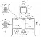
- FIG. 1depicts a lithographic apparatus according to an embodiment of the invention
- FIG. 2depicts a liquid supply system according to an embodiment of the invention
- FIG. 3is an alternative view of the liquid supply system of FIG. 2 according to an embodiment of the invention.
- FIG. 4is a view of a joint according to an embodiment of the invention.
- FIG. 5is a detailed view of the joint shown in FIG. 4 ;
- FIG. 6is a detailed view of an embodiment of the invention.
- FIG. 7is a detailed view of a joint according to an embodiment of the invention.
- FIG. 8is a detailed view of a joint according to an embodiment of the invention.
- FIG. 9is a detailed view of a joint according to another embodiment of the invention.
- FIG. 1schematically depicts a lithographic apparatus according to a particular embodiment of the invention.
- the apparatuscomprises:
- the apparatusis of a transmissive type (e.g. employing a transmissive mask).
- the apparatusmay be of a reflective type (e.g. employing a programmable mirror array of a type as referred to above).
- the illuminator ILreceives a beam of radiation from a radiation source.
- the source and the lithographic apparatusmay be separate entities, for example when the source is an excimer laser. In such cases, the source is not considered to form part of the lithographic apparatus and the radiation beam is passed from the source to the illuminator IL with the aid of a beam delivery system comprising for example suitable directing mirrors and/or a beam expander. In other cases the source may be integral part of the apparatus, for example when the source is a mercury lamp.
- the source and the illuminator IL, together with the beam delivery system if required,may be referred to as a radiation system.
- the illuminator ILmay comprise adjusting means for adjusting the angular intensity distribution of the beam. Generally, at least the outer and/or inner radial extent (commonly referred to as ⁇ -outer and ⁇ -inner, respectively) of the intensity distribution in a pupil plane of the illuminator can be adjusted.
- the illuminator ILgenerally comprises various other components, such as an integrator IN and a condenser CO.
- the illuminatorprovides a conditioned beam of radiation, referred to as the projection beam PB, having a desired uniformity and intensity distribution in its cross-section.
- the projection beam PBis incident on the mask MA, which is held on the mask table MT. Having traversed the mask MA, the projection beam PB passes through the lens PL, which focuses the beam onto a target portion C of the substrate W.
- the substrate table WTcan be moved accurately, e.g. so as to position different target portions C in the path of the beam PB.
- the first positioning means and another position sensorcan be used to accurately position the mask MA with respect to the path of the beam PB, e.g. after mechanical retrieval from a mask library, or during a scan.
- the mask table MTmay be connected to a short stroke actuator only, or may be fixed.
- Mask MA and substrate Wmay be aligned using mask alignment marks M 1 , M 2 and substrate alignment marks P 1 , P 2 .
- the depicted apparatuscan be used in the following modes:
- step modethe mask table MT and the substrate table WT are kept essentially stationary, while an entire pattern imparted to the projection beam is projected onto a target portion C in one go (i.e. a single static exposure).
- the substrate table WTis then shifted in the X and/or Y direction so that a different target portion C can be exposed.
- step modethe maximum size of the exposure field limits the size of the target portion C imaged in a single static exposure.
- the mask table MT and the substrate table WTare scanned synchronously while a pattern imparted to the projection beam is projected onto a target portion C (i.e. a single dynamic exposure).
- the velocity and direction of the substrate table WT relative to the mask table MTis determined by the (de-) magnification and image reversal characteristics of the projection system PL.
- the maximum size of the exposure fieldlimits the width (in the non-scanning direction) of the target portion in a single dynamic exposure, whereas the length of the scanning motion determines the height (in the scanning direction) of the target portion.
- the mask table MTis kept essentially stationary holding a programmable patterning device, and the substrate table WT is moved or scanned while a pattern imparted to the projection beam is projected onto a target portion C.
- a pulsed radiation sourceis employed and the programmable patterning device is updated as required after each movement of the substrate table WT or in between successive radiation pulses during a scan.
- This mode of operationcan be readily applied to maskless lithography that utilizes a programmable patterning device, such as a programmable mirror array of a type as referred to above.
- liquid supply systemwith a seal member which extends along at least a part of a boundary of the space between the final element of the projection system and the substrate table.
- the seal memberis substantially stationary relative to the projection system in the XY plane though there may be some relative movement in the Z direction (in the direction of the optical axis).
- a sealis formed between the seal member and the surface of the substrate.
- the sealis a contactless seal such as a gas seal.
- the final element, e.g. a lens 21 , of the projection systemis shown together with its support 22 .
- both the lens 21 and the support 22are made of fused silica but could be made of another glass or any other transparent material.
- the lens 21 and the support 22need not be made of the same material. Ideally, however, their expansion coefficients should be similar. For example, a higher quality material may be used for the lens 21 and a lower quality material for the support 22 .
- a glue 23joins the lens 21 and the support 22 together. Once the glue has set a liquid tight layer of glue protection 24 is applied to the joint. The glue protection 24 is applied to the entire joint. No parts are left uncovered.
- the surfaces of the lens 21 and the support 22 to be joinedare smoother and physically and chemically cleaned.
- the surfacesare so clean and smooth that the molecules in the lens 21 and support 22 begin to interact chemically by so-called “direct bonding”, forming a bond between the lens and support.
- direct bondingforming a bond between the lens and support.
- the lens 21 and support 22can be pressed together for a time. This type of bonding is particularly suitable for this situation as it produces minimal distortion of the original materials, maintains the qualities of the original materials and is strong.
- glue sealing 25can be applied to the joint followed by glue protection 24 covering the entire of the joint area.
- the jointcan also be made warm.
- a bond between the lens and supporthas been made by joining two physically and chemically clean surfaces, as in FIG. 6 and then heat treated at 900° C. for at least one hour, in an embodiment at least six hours.
- the bonds between the lens 21 and support 22then become covalent bonds which are particularly strong and watertight, as described in Materials Science Engineering incorporated herein in its entirety.
- the (glass) lens 21 and/or support 22can be covered by a thin layer of boron prior to the bonding.
- the borondiffuses into the lens 21 and/or support 22 where it aids bonding of the molecules concerned and reduces local stresses and strains. Annealing can therefore take place at a lower temperature than if boron were not present and covalent bonds will still be formed. This process is described in more detail in Philips Journal of Research 49 (1995) pages 152-153, incorporated herein in it entirety by reference.
- the jointhas been made by bonding two physically and chemically clean surfaces (as in FIGS. 6 and 7 ) and then sealed with a low temperature solder 27 .
- the soldershould have the same composition as the lens 21 and the support 22 .
- the jointis then heat treated at about 600° C.
- an indium solder 28is used between the lens 21 and the support 22 .
- indiumis used in an embodiment, other metals can also be used.
Landscapes
- Physics & Mathematics (AREA)
- General Physics & Mathematics (AREA)
- Health & Medical Sciences (AREA)
- Engineering & Computer Science (AREA)
- Environmental & Geological Engineering (AREA)
- Epidemiology (AREA)
- Public Health (AREA)
- Exposure And Positioning Against Photoresist Photosensitive Materials (AREA)
- Exposure Of Semiconductors, Excluding Electron Or Ion Beam Exposure (AREA)
- Joining Of Glass To Other Materials (AREA)
Abstract
Description
- The present invention relates to a lithographic apparatus.
- A lithographic apparatus is a machine that applies a desired pattern onto a target portion of a substrate. Lithographic apparatus can be used, for example, in the manufacture of integrated circuits (ICs). In that circumstance, a patterning device, such as a mask, may be used to generate a circuit pattern corresponding to an individual layer of the IC, and this pattern can be imaged onto a target portion (e.g. comprising part of, one or several dies) on a substrate (e.g. a silicon wafer) that has a layer of radiation-sensitive material (resist). In general, a single substrate will contain a network of adjacent target portions that are successively exposed. Known lithographic apparatus include so-called steppers, in which each target portion is irradiated by exposing an entire pattern onto the target portion in one go, and so-called scanners, in which each target portion is irradiated by scanning the pattern through the projection beam in a given direction (the “scanning”-direction) while synchronously scanning the substrate parallel or anti-parallel to this direction.
- It has been proposed to immerse the substrate in the lithographic projection apparatus in a liquid having a relatively high refractive index, e.g. water, so as to fill a space between the final element of the projection system and the substrate. The point of this is to enable imaging of smaller features since the exposure radiation will have a shorter wavelength in the liquid. (The effect of the liquid may also be regarded as increasing the effective NA of the system and also increasing the depth of focus.)
- However, submersing the substrate or substrate and substrate table in a bath of liquid (see for example U.S. Pat. No. 4,509,852, hereby incorporated in its entirety by reference) may mean that there is a large body of liquid that should be accelerated during a scanning exposure. This may require additional or more powerful motors and turbulence in the liquid may lead to undesirable and unpredictable effects. Also, the optical properties, in particular the geometrical optical properties of the elements of the projection system should remain constant.
- One of the solutions proposed is for a liquid supply system to provide liquid on only a localized area of the substrate and in between the final element of the projection system and the substrate using a liquid supply system (the substrate generally has a larger surface area than the final element of the projection system). One way which has been proposed to arrange for this is disclosed in PCT patent application WO 99/49504, hereby incorporated in its entirety by reference. As illustrated in
FIGS. 2 and 3 , liquid is supplied by at least one inlet IN onto the substrate, in an embodiment along the direction of movement of the substrate relative to the final element, and is removed by at least one outlet OUT after having passed under the projection system. That is, as the substrate is scanned beneath the element in a −X direction, liquid is supplied at the +X side of the element and taken up at the −X side.FIG. 2 shows the arrangement schematically in which liquid is supplied via inlet IN and is taken up on the other side of the element by outlet OUT which is connected to a low pressure source. In the illustration ofFIG. 2 the liquid is supplied along the direction of movement of the substrate relative to the final element, though this does not need to be the case. Various orientations and numbers of in- and out-lets positioned around the final element are possible, one example is illustrated inFIG. 3 in which four sets of an inlet with an outlet on either side are provided in a regular pattern around the final element. - The presence of fluid around the bottom of a projection system may deform elements of the projection system possibly leading to degradation of exposure. Further, the liquid may enter into the projection system which can damage or deform delicate parts of the apparatus over time.
- Accordingly, it would be advantageous to provide, for example, an apparatus in which distortion of the projection system due to the presence of liquid is minimized.
- According to an aspect, there is provided a lithographic apparatus comprising:
- a support structure configured to hold a patterning device, the patterning device configured to pattern a projection beam with a pattern in its cross-section;
- a substrate table configured to hold a substrate; and
- a projection system configured to project the patterned beam onto a target portion of the substrate, wherein a joint between an element of the projection system and its support comprises an inorganic layer.
- By making a joint liquid tight, i.e., no liquid can enter the projection system, deformation of projection system element, such as a lens, may be minimized. In particular, deformation of the element should be limited to the amount by which lens elements can compensate for the distortion.
- In an embodiment, the joint can comprise a direct bond. Direct bonding is used as a broad term and encompasses fusion bonding, anodic bonding, compression bonding etc.
- The inorganic layer can be a metal, ceramic or glass layer or glue protection. The element of the projection system and its support can be made of glass, bonding of which is relatively simple. In an embodiment, the element and its support are made of fused silica.
- The apparatus may further comprise a liquid supply system configured to at least partly fill a space between the projection system and the substrate, with a liquid.
- In an embodiment, the joints between all parts of the projection system immersed in liquid comprise an inorganic layer. Liquid can be prevented from entering the projection system or weakening any of the joints. The joint can be made liquid resistant by applying an inorganic layer to the joint.
- The joint can be made without any heating. For example, the joint can be made liquid tight by applying a liquid resistant layer to the joint. The joint between the element of the projection system and its support (and other joints) can be made using glue (which need not be liquid resistant) or by the interaction of physically and chemically clean surfaces. To clean the surfaces, a solvent could be applied or the surfaces freshly cleaved. After a bonding, an inorganic layer could then be applied to the joint.
- Alternatively, the joint can be heat treated. The joint may be heated to about 900° C., in an embodiment for at least one hour. Again, the joint can be made by the interaction of clean surfaces. For improved results, the glass may be doped with boron. An alternative warm joint is made by the interaction of clean surfaces, sealed with a low temperature glass solder and then heat treated to 600° C. A further type of warm joint is a metal solder. Indium solder has been found to work particularly well.
- According to an aspect, there is provided a lithographic apparatus comprising:
- a support structure configured to hold a patterning device, the patterning device configured to pattern a projection beam with a pattern in its cross-section;
- a substrate table configured to hold a substrate; and
- a projection system configured to projecting the patterned beam onto a target portion of the substrate, wherein a joint between an of the projection system and its support comprises a direct bond.
- According to an aspect, there is provided an immersion projection system manufacturing method comprising joining an element of a projection system, that in use in a lithographic apparatus comes into contact with a liquid, with its support using at least one of an inorganic layer or direct bonding.
- According to an aspect, there is provided a device manufacturing method comprising projecting a patterned beam of radiation onto a target portion of the substrate through an element of a projection system joined to its support using at least one of an inorganic layer or direct bonding.
- Although specific reference may be made in this text to the use of lithographic apparatus in the manufacture of ICs, it should be understood that the lithographic apparatus described herein may have other applications, such as the manufacture of integrated optical systems, guidance and detection patterns for magnetic domain memories, liquid-crystal displays (LCDs), thin-film magnetic heads, etc. The skilled artisan will appreciate that, in the context of such alternative applications, any use of the terms “wafer” or “die” herein may be considered as synonymous with the more general terms “substrate” or “target portion”, respectively. The substrate referred to herein may be processed, before or after exposure, in for example a track (a tool that typically applies a layer of resist to a substrate and develops the exposed resist) or a metrology or inspection tool. Where applicable, the disclosure herein may be applied to such and other substrate processing tools. Further, the substrate may be processed more than once, for example in order to create a multi-layer IC, so that the term substrate used herein may also refer to a substrate that already contains multiple processed layers.
- The terms “radiation” and “beam” used herein encompass all types of electromagnetic radiation, including ultraviolet (UV) radiation (e.g. having a wavelength of 365, 248, 193, 157 or 126 nm).
- The term “patterning device” used herein should be broadly interpreted as referring to any device that can be used to impart a projection beam with a pattern in its cross-section such as to create a pattern in a target portion of the substrate. It should be noted that the pattern imparted to the projection beam may not exactly correspond to the desired pattern in the target portion of the substrate. Generally, the pattern imparted to the projection beam will correspond to a particular functional layer in a device being created in the target portion, such as an integrated circuit.
- A patterning device may be transmissive or reflective. Examples of a patterning device include masks, programmable mirror arrays, and programmable LCD panels. Masks are well known in lithography, and include mask types such as binary, alternating phase-shift, and attenuated phase-shift, as well as various hybrid mask types. An example of a programmable mirror array employs a matrix arrangement of small mirrors, each of which can be individually tilted so as to reflect an incoming radiation beam in different directions; in this manner, the reflected beam is patterned. In each example of a patterning device, the support structure may be a frame or table, for example, which may be fixed or movable as required and which may ensure that the patterning device is at a desired position, for example with respect to the projection system. Any use of the terms “reticle” or “mask” herein may be considered synonymous with the more general term “patterning device”.
- The term “projection system” used herein should be broadly interpreted as encompassing various types of projection system, including refractive optical systems, reflective optical systems, and catadioptric optical systems, as appropriate for example for the exposure radiation being used, or for other factors such as the use of an immersion fluid or the use of a vacuum. Any use of the term “lens” herein may be considered as synonymous with the more general term “projection system”.
- The illumination system may also encompass various types of optical components, including refractive, reflective, and catadioptric optical components for directing, shaping, or controlling the projection beam of radiation, and such components may also be referred to below, collectively or singularly, as a “lens”.
- The lithographic apparatus may be of a type having two (dual stage) or more substrate tables (and/or two or more mask tables). In such “multiple stage” machines the additional tables may be used in parallel, or preparatory steps may be carried out on one or more tables while one or more other tables are being used for exposure.
- Embodiments of the invention will now be described, by way of example only, with reference to the accompanying schematic drawings in which corresponding reference symbols indicate corresponding parts, and in which:
FIG. 1 depicts a lithographic apparatus according to an embodiment of the invention;FIG. 2 depicts a liquid supply system according to an embodiment of the invention;FIG. 3 is an alternative view of the liquid supply system ofFIG. 2 according to an embodiment of the invention;FIG. 4 is a view of a joint according to an embodiment of the invention;FIG. 5 is a detailed view of the joint shown inFIG. 4 ;FIG. 6 is a detailed view of an embodiment of the invention;FIG. 7 is a detailed view of a joint according to an embodiment of the invention;FIG. 8 is a detailed view of a joint according to an embodiment of the invention; andFIG. 9 is a detailed view of a joint according to another embodiment of the invention.FIG. 1 schematically depicts a lithographic apparatus according to a particular embodiment of the invention. The apparatus comprises:- an illumination system (illuminator) IL for providing a projection beam PB of radiation (e.g. UV radiation);
- a first support structure (e.g. a mask table) MT for supporting a patterning device (e.g. a mask) MA and connected to first positioning means for accurately positioning the patterning device with respect to item PL;
- a substrate table (e.g. a wafer table) WT for holding a substrate (e.g. a resist-coated wafer) W and connected to second positioning means for accurately positioning the substrate with respect to item PL; and
- a projection system (e.g. a refractive projection lens) PL for imaging a pattern imparted to the projection beam PB by patterning device MA onto a target portion C (e.g. comprising one or more dies) of the substrate W.
- As here depicted, the apparatus is of a transmissive type (e.g. employing a transmissive mask). Alternatively, the apparatus may be of a reflective type (e.g. employing a programmable mirror array of a type as referred to above).
- The illuminator IL receives a beam of radiation from a radiation source. The source and the lithographic apparatus may be separate entities, for example when the source is an excimer laser. In such cases, the source is not considered to form part of the lithographic apparatus and the radiation beam is passed from the source to the illuminator IL with the aid of a beam delivery system comprising for example suitable directing mirrors and/or a beam expander. In other cases the source may be integral part of the apparatus, for example when the source is a mercury lamp. The source and the illuminator IL, together with the beam delivery system if required, may be referred to as a radiation system.
- The illuminator IL may comprise adjusting means for adjusting the angular intensity distribution of the beam. Generally, at least the outer and/or inner radial extent (commonly referred to as σ-outer and σ-inner, respectively) of the intensity distribution in a pupil plane of the illuminator can be adjusted. In addition, the illuminator IL generally comprises various other components, such as an integrator IN and a condenser CO. The illuminator provides a conditioned beam of radiation, referred to as the projection beam PB, having a desired uniformity and intensity distribution in its cross-section.
- The projection beam PB is incident on the mask MA, which is held on the mask table MT. Having traversed the mask MA, the projection beam PB passes through the lens PL, which focuses the beam onto a target portion C of the substrate W. With the aid of the second positioning means and position sensor IF (e.g. an interferometric device), the substrate table WT can be moved accurately, e.g. so as to position different target portions C in the path of the beam PB. Similarly, the first positioning means and another position sensor (which is not explicitly depicted in
FIG. 1 ) can be used to accurately position the mask MA with respect to the path of the beam PB, e.g. after mechanical retrieval from a mask library, or during a scan. In general, movement of the object tables MT and WT will be realized with the aid of a long-stroke module (coarse positioning) and a short-stroke module (fine positioning), which form part of the positioning means. However, in the case of a stepper (as opposed to a scanner) the mask table MT may be connected to a short stroke actuator only, or may be fixed. Mask MA and substrate W may be aligned using mask alignment marks M1, M2 and substrate alignment marks P1, P2. - The depicted apparatus can be used in the following modes:
- 1. In step mode, the mask table MT and the substrate table WT are kept essentially stationary, while an entire pattern imparted to the projection beam is projected onto a target portion C in one go (i.e. a single static exposure). The substrate table WT is then shifted in the X and/or Y direction so that a different target portion C can be exposed. In step mode, the maximum size of the exposure field limits the size of the target portion C imaged in a single static exposure.
- 2. In scan mode, the mask table MT and the substrate table WT are scanned synchronously while a pattern imparted to the projection beam is projected onto a target portion C (i.e. a single dynamic exposure). The velocity and direction of the substrate table WT relative to the mask table MT is determined by the (de-) magnification and image reversal characteristics of the projection system PL. In scan mode, the maximum size of the exposure field limits the width (in the non-scanning direction) of the target portion in a single dynamic exposure, whereas the length of the scanning motion determines the height (in the scanning direction) of the target portion.
- 3. In another mode, the mask table MT is kept essentially stationary holding a programmable patterning device, and the substrate table WT is moved or scanned while a pattern imparted to the projection beam is projected onto a target portion C. In this mode, generally a pulsed radiation source is employed and the programmable patterning device is updated as required after each movement of the substrate table WT or in between successive radiation pulses during a scan. This mode of operation can be readily applied to maskless lithography that utilizes a programmable patterning device, such as a programmable mirror array of a type as referred to above.
- Combinations and/or variations on the above described modes of use or entirely different modes of use may also be employed.
- In addition to the liquid supply solutions described above, another solution which has been proposed is to provide the liquid supply system with a seal member which extends along at least a part of a boundary of the space between the final element of the projection system and the substrate table. The seal member is substantially stationary relative to the projection system in the XY plane though there may be some relative movement in the Z direction (in the direction of the optical axis). A seal is formed between the seal member and the surface of the substrate. In an embodiment, the seal is a contactless seal such as a gas seal. Such a system is disclosed in European Patent Application No. 03252955.4 and U.S. patent application Ser. No. 10/705,783, hereby incorporated in its entirety by reference.
- In
FIGS. 4 and 5 , the final element, e.g. alens 21, of the projection system is shown together with itssupport 22. In this example both thelens 21 and thesupport 22 are made of fused silica but could be made of another glass or any other transparent material. Indeed thelens 21 and thesupport 22 need not be made of the same material. Ideally, however, their expansion coefficients should be similar. For example, a higher quality material may be used for thelens 21 and a lower quality material for thesupport 22. Aglue 23 joins thelens 21 and thesupport 22 together. Once the glue has set a liquid tight layer ofglue protection 24 is applied to the joint. Theglue protection 24 is applied to the entire joint. No parts are left uncovered. - In
FIG. 6 , the surfaces of thelens 21 and thesupport 22 to be joined are smoother and physically and chemically cleaned. The surfaces are so clean and smooth that the molecules in thelens 21 andsupport 22 begin to interact chemically by so-called “direct bonding”, forming a bond between the lens and support. To assist and expedite this process thelens 21 andsupport 22 can be pressed together for a time. This type of bonding is particularly suitable for this situation as it produces minimal distortion of the original materials, maintains the qualities of the original materials and is strong. Additionally, glue sealing25 can be applied to the joint followed byglue protection 24 covering the entire of the joint area. - The joint can also be made warm. In
FIG. 7 , a bond between the lens and support has been made by joining two physically and chemically clean surfaces, as inFIG. 6 and then heat treated at 900° C. for at least one hour, in an embodiment at least six hours. The bonds between thelens 21 andsupport 22 then become covalent bonds which are particularly strong and watertight, as described in Materials Science Engineering incorporated herein in its entirety. The (glass)lens 21 and/orsupport 22 can be covered by a thin layer of boron prior to the bonding. The boron diffuses into thelens 21 and/orsupport 22 where it aids bonding of the molecules concerned and reduces local stresses and strains. Annealing can therefore take place at a lower temperature than if boron were not present and covalent bonds will still be formed. This process is described in more detail in Philips Journal of Research 49 (1995) pages 152-153, incorporated herein in it entirety by reference. - In
FIG. 8 , the joint has been made by bonding two physically and chemically clean surfaces (as inFIGS. 6 and 7 ) and then sealed with alow temperature solder 27. The solder should have the same composition as thelens 21 and thesupport 22. The joint is then heat treated at about 600° C. - In
FIG. 9 anindium solder 28 is used between thelens 21 and thesupport 22. Although indium is used in an embodiment, other metals can also be used. - Although the joint between the
lens 21 and itssupport 22 has been described here it will be obvious to the skilled person that the same technology can be applied to any other joint in the projection system, and indeed in the lithographic apparatus. In particular, all joints which may come into contact with the immersion liquid should be made liquid tight by one of the methods described above. - While specific embodiments of the invention have been described above, it will be appreciated that the invention may be practiced otherwise than as described. The description is not intended to limit the invention.
Claims (21)
Priority Applications (1)
| Application Number | Priority Date | Filing Date | Title |
|---|---|---|---|
| US12/463,242US8472006B2 (en) | 2003-11-24 | 2009-05-08 | Lithographic apparatus and device manufacturing method |
Applications Claiming Priority (2)
| Application Number | Priority Date | Filing Date | Title |
|---|---|---|---|
| US10/719,683US7545481B2 (en) | 2003-11-24 | 2003-11-24 | Lithographic apparatus and device manufacturing method |
| US12/463,242US8472006B2 (en) | 2003-11-24 | 2009-05-08 | Lithographic apparatus and device manufacturing method |
Related Parent Applications (1)
| Application Number | Title | Priority Date | Filing Date |
|---|---|---|---|
| US10/719,683ContinuationUS7545481B2 (en) | 2003-11-24 | 2003-11-24 | Lithographic apparatus and device manufacturing method |
Publications (2)
| Publication Number | Publication Date |
|---|---|
| US20090214986A1true US20090214986A1 (en) | 2009-08-27 |
| US8472006B2 US8472006B2 (en) | 2013-06-25 |
Family
ID=34591399
Family Applications (2)
| Application Number | Title | Priority Date | Filing Date |
|---|---|---|---|
| US10/719,683Expired - Fee RelatedUS7545481B2 (en) | 2003-11-24 | 2003-11-24 | Lithographic apparatus and device manufacturing method |
| US12/463,242Expired - Fee RelatedUS8472006B2 (en) | 2003-11-24 | 2009-05-08 | Lithographic apparatus and device manufacturing method |
Family Applications Before (1)
| Application Number | Title | Priority Date | Filing Date |
|---|---|---|---|
| US10/719,683Expired - Fee RelatedUS7545481B2 (en) | 2003-11-24 | 2003-11-24 | Lithographic apparatus and device manufacturing method |
Country Status (4)
| Country | Link |
|---|---|
| US (2) | US7545481B2 (en) |
| CN (1) | CN1906541A (en) |
| TW (1) | TWI261150B (en) |
| WO (1) | WO2005054955A2 (en) |
Families Citing this family (142)
| Publication number | Priority date | Publication date | Assignee | Title |
|---|---|---|---|---|
| KR100585476B1 (en)* | 2002-11-12 | 2006-06-07 | 에이에스엠엘 네델란즈 비.브이. | Lithographic Apparatus and Device Manufacturing Method |
| US7372541B2 (en) | 2002-11-12 | 2008-05-13 | Asml Netherlands B.V. | Lithographic apparatus and device manufacturing method |
| US10503084B2 (en) | 2002-11-12 | 2019-12-10 | Asml Netherlands B.V. | Lithographic apparatus and device manufacturing method |
| US9482966B2 (en) | 2002-11-12 | 2016-11-01 | Asml Netherlands B.V. | Lithographic apparatus and device manufacturing method |
| US7110081B2 (en) | 2002-11-12 | 2006-09-19 | Asml Netherlands B.V. | Lithographic apparatus and device manufacturing method |
| SG121822A1 (en)* | 2002-11-12 | 2006-05-26 | Asml Netherlands Bv | Lithographic apparatus and device manufacturing method |
| DE60335595D1 (en)* | 2002-11-12 | 2011-02-17 | Asml Netherlands Bv | Immersion lithographic apparatus and method of making a device |
| CN100568101C (en) | 2002-11-12 | 2009-12-09 | Asml荷兰有限公司 | Photolithography apparatus and device manufacturing method |
| KR20120127755A (en)* | 2002-12-10 | 2012-11-23 | 가부시키가이샤 니콘 | Exposure apparatus and method for manufacturing device |
| US7948604B2 (en)* | 2002-12-10 | 2011-05-24 | Nikon Corporation | Exposure apparatus and method for producing device |
| WO2004053955A1 (en)* | 2002-12-10 | 2004-06-24 | Nikon Corporation | Exposure system and device producing method |
| US7242455B2 (en)* | 2002-12-10 | 2007-07-10 | Nikon Corporation | Exposure apparatus and method for producing device |
| KR101101737B1 (en)* | 2002-12-10 | 2012-01-05 | 가부시키가이샤 니콘 | Exposure apparatus, exposure method and method for manufacturing device |
| JP4352874B2 (en)* | 2002-12-10 | 2009-10-28 | 株式会社ニコン | Exposure apparatus and device manufacturing method |
| EP1571694A4 (en)* | 2002-12-10 | 2008-10-15 | Nikon Corp | Exposure apparatus and method for manufacturing device |
| DE10261775A1 (en) | 2002-12-20 | 2004-07-01 | Carl Zeiss Smt Ag | Device for the optical measurement of an imaging system |
| EP2466623B1 (en) | 2003-02-26 | 2015-04-22 | Nikon Corporation | Exposure apparatus, exposure method, and method for producing device |
| KR20050110033A (en)* | 2003-03-25 | 2005-11-22 | 가부시키가이샤 니콘 | Exposure system and device production method |
| EP1612850B1 (en)* | 2003-04-07 | 2009-03-25 | Nikon Corporation | Exposure apparatus and method for manufacturing a device |
| WO2004093159A2 (en)* | 2003-04-09 | 2004-10-28 | Nikon Corporation | Immersion lithography fluid control system |
| EP3062152B1 (en)* | 2003-04-10 | 2017-12-20 | Nikon Corporation | Environmental system including vaccum scavenge for an immersion lithography apparatus |
| WO2004090633A2 (en)* | 2003-04-10 | 2004-10-21 | Nikon Corporation | An electro-osmotic element for an immersion lithography apparatus |
| EP3352010A1 (en)* | 2003-04-10 | 2018-07-25 | Nikon Corporation | Run-off path to collect liquid for an immersion lithography apparatus |
| EP2950147B1 (en) | 2003-04-10 | 2017-04-26 | Nikon Corporation | Environmental system including vaccum scavenge for an immersion lithography apparatus |
| KR101225884B1 (en) | 2003-04-11 | 2013-01-28 | 가부시키가이샤 니콘 | Apparatus and method for maintaining immersion fluid in the gap under the projection lens during wafer exchange in an immersion lithography machine |
| CN101825847B (en) | 2003-04-11 | 2013-10-16 | 株式会社尼康 | Cleanup method for optics in immersion lithography |
| JP4582089B2 (en) | 2003-04-11 | 2010-11-17 | 株式会社ニコン | Liquid jet recovery system for immersion lithography |
| SG194246A1 (en) | 2003-04-17 | 2013-11-29 | Nikon Corp | Optical arrangement of autofocus elements for use with immersion lithography |
| TWI295414B (en) | 2003-05-13 | 2008-04-01 | Asml Netherlands Bv | Lithographic apparatus and device manufacturing method |
| KR20060009356A (en)* | 2003-05-15 | 2006-01-31 | 가부시키가이샤 니콘 | Exposure apparatus and device manufacturing method |
| TW201806001A (en)* | 2003-05-23 | 2018-02-16 | 尼康股份有限公司 | Exposure device and device manufacturing method |
| TWI421906B (en)* | 2003-05-23 | 2014-01-01 | 尼康股份有限公司 | An exposure method, an exposure apparatus, and an element manufacturing method |
| KR101548832B1 (en)* | 2003-05-28 | 2015-09-01 | 가부시키가이샤 니콘 | Exposure method, exposure device, and device manufacturing method |
| TWI442694B (en)* | 2003-05-30 | 2014-06-21 | Asml Netherlands Bv | Lithographic apparatus and device manufacturing method |
| US7213963B2 (en) | 2003-06-09 | 2007-05-08 | Asml Netherlands B.V. | Lithographic apparatus and device manufacturing method |
| US7317504B2 (en)* | 2004-04-08 | 2008-01-08 | Asml Netherlands B.V. | Lithographic apparatus and device manufacturing method |
| EP2261741A3 (en) | 2003-06-11 | 2011-05-25 | ASML Netherlands B.V. | Lithographic apparatus and device manufacturing method |
| KR101242815B1 (en)* | 2003-06-13 | 2013-03-12 | 가부시키가이샤 니콘 | Exposure method, substrate stage, exposure apparatus and method for manufacturing device |
| TW201721717A (en) | 2003-06-19 | 2017-06-16 | 尼康股份有限公司 | Exposure apparatus, exposure method, and device manufacturing method |
| KR20060027832A (en)* | 2003-07-01 | 2006-03-28 | 가부시키가이샤 니콘 | Method of Using Isotopically Specified Fluids as Optical Elements |
| EP3179309A1 (en)* | 2003-07-08 | 2017-06-14 | Nikon Corporation | Wafer table for immersion lithography |
| EP1643543B1 (en)* | 2003-07-09 | 2010-11-24 | Nikon Corporation | Exposure apparatus and method for manufacturing device |
| WO2005006415A1 (en)* | 2003-07-09 | 2005-01-20 | Nikon Corporation | Exposure apparatus and method for manufacturing device |
| WO2005006418A1 (en)* | 2003-07-09 | 2005-01-20 | Nikon Corporation | Exposure apparatus and method for manufacturing device |
| SG109000A1 (en)* | 2003-07-16 | 2005-02-28 | Asml Netherlands Bv | Lithographic apparatus and device manufacturing method |
| EP1500982A1 (en)* | 2003-07-24 | 2005-01-26 | ASML Netherlands B.V. | Lithographic apparatus and device manufacturing method |
| WO2005010960A1 (en)* | 2003-07-25 | 2005-02-03 | Nikon Corporation | Inspection method and inspection device for projection optical system, and production method for projection optical system |
| KR101641011B1 (en)* | 2003-07-28 | 2016-07-19 | 가부시키가이샤 니콘 | Exposure apparatus, device producing method, and exposure apparatus controlling method |
| US7175968B2 (en) | 2003-07-28 | 2007-02-13 | Asml Netherlands B.V. | Lithographic apparatus, device manufacturing method and a substrate |
| US7326522B2 (en) | 2004-02-11 | 2008-02-05 | Asml Netherlands B.V. | Device manufacturing method and a substrate |
| EP1503244A1 (en) | 2003-07-28 | 2005-02-02 | ASML Netherlands B.V. | Lithographic projection apparatus and device manufacturing method |
| US7779781B2 (en) | 2003-07-31 | 2010-08-24 | Asml Netherlands B.V. | Lithographic apparatus and device manufacturing method |
| US8149381B2 (en)* | 2003-08-26 | 2012-04-03 | Nikon Corporation | Optical element and exposure apparatus |
| JP4474652B2 (en)* | 2003-08-26 | 2010-06-09 | 株式会社ニコン | Optical element and exposure apparatus |
| EP2261740B1 (en) | 2003-08-29 | 2014-07-09 | ASML Netherlands BV | Lithographic apparatus |
| TWI263859B (en) | 2003-08-29 | 2006-10-11 | Asml Netherlands Bv | Lithographic apparatus and device manufacturing method |
| TWI245163B (en) | 2003-08-29 | 2005-12-11 | Asml Netherlands Bv | Lithographic apparatus and device manufacturing method |
| KR101380989B1 (en)* | 2003-08-29 | 2014-04-04 | 가부시키가이샤 니콘 | Exposure apparatus and device producing method |
| EP3223053A1 (en)* | 2003-09-03 | 2017-09-27 | Nikon Corporation | Apparatus and method for providing fluid for immersion lithography |
| JP4444920B2 (en)* | 2003-09-19 | 2010-03-31 | 株式会社ニコン | Exposure apparatus and device manufacturing method |
| EP2837969B1 (en) | 2003-09-29 | 2016-04-20 | Nikon Corporation | Exposure apparatus, exposure method, and method for producing device |
| KR20060126949A (en) | 2003-10-08 | 2006-12-11 | 가부시키가이샤 니콘 | Substrate conveyance apparatus and substrate conveyance method, exposure apparatus, exposure method, and device manufacturing method |
| JP2005136364A (en)* | 2003-10-08 | 2005-05-26 | Zao Nikon Co Ltd | Substrate transport apparatus, exposure apparatus, and device manufacturing method |
| KR101203028B1 (en) | 2003-10-08 | 2012-11-21 | 가부시키가이샤 자오 니콘 | Substrate carrying apparatus, substrate carrying method, exposure apparatus, exposure method, and method for producing device |
| TWI553701B (en) | 2003-10-09 | 2016-10-11 | 尼康股份有限公司 | Exposure apparatus and exposure method, component manufacturing method |
| EP1524557A1 (en) | 2003-10-15 | 2005-04-20 | ASML Netherlands B.V. | Lithographic apparatus and device manufacturing method |
| EP1524558A1 (en) | 2003-10-15 | 2005-04-20 | ASML Netherlands B.V. | Lithographic apparatus and device manufacturing method |
| US7352433B2 (en) | 2003-10-28 | 2008-04-01 | Asml Netherlands B.V. | Lithographic apparatus and device manufacturing method |
| US7411653B2 (en)* | 2003-10-28 | 2008-08-12 | Asml Netherlands B.V. | Lithographic apparatus |
| US7528929B2 (en) | 2003-11-14 | 2009-05-05 | Asml Netherlands B.V. | Lithographic apparatus and device manufacturing method |
| US7545481B2 (en)* | 2003-11-24 | 2009-06-09 | Asml Netherlands B.V. | Lithographic apparatus and device manufacturing method |
| KR101394764B1 (en) | 2003-12-03 | 2014-05-27 | 가부시키가이샤 니콘 | Exposure apparatus, exposure method, device producing method, and optical component |
| JPWO2005057635A1 (en)* | 2003-12-15 | 2007-07-05 | 株式会社ニコン | Projection exposure apparatus, stage apparatus, and exposure method |
| US20070081133A1 (en)* | 2004-12-14 | 2007-04-12 | Niikon Corporation | Projection exposure apparatus and stage unit, and exposure method |
| JP4720506B2 (en) | 2003-12-15 | 2011-07-13 | 株式会社ニコン | Stage apparatus, exposure apparatus, and exposure method |
| US7589818B2 (en)* | 2003-12-23 | 2009-09-15 | Asml Netherlands B.V. | Lithographic apparatus, alignment apparatus, device manufacturing method, and a method of converting an apparatus |
| US7394521B2 (en)* | 2003-12-23 | 2008-07-01 | Asml Netherlands B.V. | Lithographic apparatus and device manufacturing method |
| DE602005019689D1 (en)* | 2004-01-20 | 2010-04-15 | Zeiss Carl Smt Ag | EXPOSURE DEVICE AND MEASURING DEVICE FOR A PROJECTION SECTOR |
| US7589822B2 (en) | 2004-02-02 | 2009-09-15 | Nikon Corporation | Stage drive method and stage unit, exposure apparatus, and device manufacturing method |
| WO2005076321A1 (en) | 2004-02-03 | 2005-08-18 | Nikon Corporation | Exposure apparatus and method of producing device |
| US7050146B2 (en) | 2004-02-09 | 2006-05-23 | Asml Netherlands B.V. | Lithographic apparatus and device manufacturing method |
| KR101851511B1 (en) | 2004-03-25 | 2018-04-23 | 가부시키가이샤 니콘 | Exposure apparatus and method for manufacturing device |
| US7034917B2 (en)* | 2004-04-01 | 2006-04-25 | Asml Netherlands B.V. | Lithographic apparatus, device manufacturing method and device manufactured thereby |
| US7898642B2 (en) | 2004-04-14 | 2011-03-01 | Asml Netherlands B.V. | Lithographic apparatus and device manufacturing method |
| US7379159B2 (en) | 2004-05-03 | 2008-05-27 | Asml Netherlands B.V. | Lithographic apparatus and device manufacturing method |
| US8054448B2 (en)* | 2004-05-04 | 2011-11-08 | Nikon Corporation | Apparatus and method for providing fluid for immersion lithography |
| US7616383B2 (en)* | 2004-05-18 | 2009-11-10 | Asml Netherlands B.V. | Lithographic apparatus and device manufacturing method |
| US7486381B2 (en)* | 2004-05-21 | 2009-02-03 | Asml Netherlands B.V. | Lithographic apparatus and device manufacturing method |
| CN100594430C (en) | 2004-06-04 | 2010-03-17 | 卡尔蔡司Smt股份公司 | System for measuring image quality of optical imaging system |
| US20070103661A1 (en)* | 2004-06-04 | 2007-05-10 | Nikon Corporation | Exposure apparatus, exposure method, and method for producing device |
| WO2005119742A1 (en)* | 2004-06-04 | 2005-12-15 | Nikon Corporation | Exposure apparatus, exposure method, and device producing method |
| EP3203498A1 (en)* | 2004-06-09 | 2017-08-09 | Nikon Corporation | Exposure apparatus and device manufacturing method |
| US20070222959A1 (en)* | 2004-06-10 | 2007-09-27 | Nikon Corporation | Exposure apparatus, exposure method, and method for producing device |
| EP3067749B1 (en)* | 2004-06-10 | 2017-10-18 | Nikon Corporation | Exposure apparatus, exposure method, and method for producing device |
| US7481867B2 (en) | 2004-06-16 | 2009-01-27 | Edwards Limited | Vacuum system for immersion photolithography |
| US7463330B2 (en) | 2004-07-07 | 2008-12-09 | Asml Netherlands B.V. | Lithographic apparatus and device manufacturing method |
| JP4894515B2 (en)* | 2004-07-12 | 2012-03-14 | 株式会社ニコン | Exposure apparatus, device manufacturing method, and liquid detection method |
| US7304715B2 (en) | 2004-08-13 | 2007-12-04 | Asml Netherlands B.V. | Lithographic apparatus and device manufacturing method |
| KR20070048164A (en)* | 2004-08-18 | 2007-05-08 | 가부시키가이샤 니콘 | Exposure apparatus and device manufacturing method |
| US7701550B2 (en) | 2004-08-19 | 2010-04-20 | Asml Netherlands B.V. | Lithographic apparatus and device manufacturing method |
| US7522261B2 (en)* | 2004-09-24 | 2009-04-21 | Asml Netherlands B.V. | Lithographic apparatus and device manufacturing method |
| US7355674B2 (en)* | 2004-09-28 | 2008-04-08 | Asml Netherlands B.V. | Lithographic apparatus, device manufacturing method and computer program product |
| US7894040B2 (en)* | 2004-10-05 | 2011-02-22 | Asml Netherlands B.V. | Lithographic apparatus and device manufacturing method |
| US7379155B2 (en)* | 2004-10-18 | 2008-05-27 | Asml Netherlands B.V. | Lithographic apparatus and device manufacturing method |
| US7414699B2 (en)* | 2004-11-12 | 2008-08-19 | Asml Netherlands B.V. | Lithographic apparatus and device manufacturing method |
| US7423720B2 (en) | 2004-11-12 | 2008-09-09 | Asml Netherlands B.V. | Lithographic apparatus and device manufacturing method |
| US7583357B2 (en)* | 2004-11-12 | 2009-09-01 | Asml Netherlands B.V. | Lithographic apparatus and device manufacturing method |
| US7397533B2 (en) | 2004-12-07 | 2008-07-08 | Asml Netherlands B.V. | Lithographic apparatus and device manufacturing method |
| US7365827B2 (en) | 2004-12-08 | 2008-04-29 | Asml Netherlands B.V. | Lithographic apparatus and device manufacturing method |
| US7403261B2 (en)* | 2004-12-15 | 2008-07-22 | Asml Netherlands B.V. | Lithographic apparatus and device manufacturing method |
| US7880860B2 (en)* | 2004-12-20 | 2011-02-01 | Asml Netherlands B.V. | Lithographic apparatus and device manufacturing method |
| US7405805B2 (en)* | 2004-12-28 | 2008-07-29 | Asml Netherlands B.V. | Lithographic apparatus and device manufacturing method |
| SG124351A1 (en)* | 2005-01-14 | 2006-08-30 | Asml Netherlands Bv | Lithographic apparatus and device manufacturing method |
| DE602006012746D1 (en)* | 2005-01-14 | 2010-04-22 | Asml Netherlands Bv | Lithographic apparatus and manufacturing method |
| KR101513840B1 (en)* | 2005-01-31 | 2015-04-20 | 가부시키가이샤 니콘 | Exposure apparatus and method for manufacturing device |
| US8692973B2 (en)* | 2005-01-31 | 2014-04-08 | Nikon Corporation | Exposure apparatus and method for producing device |
| US7282701B2 (en)* | 2005-02-28 | 2007-10-16 | Asml Netherlands B.V. | Sensor for use in a lithographic apparatus |
| US7684010B2 (en)* | 2005-03-09 | 2010-03-23 | Asml Netherlands B.V. | Lithographic apparatus, device manufacturing method, seal structure, method of removing an object and a method of sealing |
| USRE43576E1 (en) | 2005-04-08 | 2012-08-14 | Asml Netherlands B.V. | Dual stage lithographic apparatus and device manufacturing method |
| US7535644B2 (en)* | 2005-08-12 | 2009-05-19 | Asml Netherlands B.V. | Lens element, lithographic apparatus, device manufacturing method, and device manufactured thereby |
| US7357768B2 (en)* | 2005-09-22 | 2008-04-15 | William Marshall | Recliner exerciser |
| JP4514225B2 (en) | 2005-11-16 | 2010-07-28 | キヤノン株式会社 | Exposure apparatus and device manufacturing method |
| US20070124987A1 (en)* | 2005-12-05 | 2007-06-07 | Brown Jeffrey K | Electronic pest control apparatus |
| KR100768849B1 (en)* | 2005-12-06 | 2007-10-22 | 엘지전자 주식회사 | Power supply system and method for grid-connected fuel cell system |
| US7649611B2 (en) | 2005-12-30 | 2010-01-19 | Asml Netherlands B.V. | Lithographic apparatus and device manufacturing method |
| US7893047B2 (en)* | 2006-03-03 | 2011-02-22 | Arch Chemicals, Inc. | Biocide composition comprising pyrithione and pyrrole derivatives |
| DE102006021797A1 (en) | 2006-05-09 | 2007-11-15 | Carl Zeiss Smt Ag | Optical imaging device with thermal damping |
| DE102006050653A1 (en)* | 2006-10-24 | 2008-04-30 | Carl Zeiss Smt Ag | Method for connecting an optical element with a fitting on at least one connecting site used in semiconductor lithography comprises indirectly or directly positioning the element and the fitting during connection using a support element |
| US8654305B2 (en)* | 2007-02-15 | 2014-02-18 | Asml Holding N.V. | Systems and methods for insitu lens cleaning in immersion lithography |
| US8817226B2 (en) | 2007-02-15 | 2014-08-26 | Asml Holding N.V. | Systems and methods for insitu lens cleaning using ozone in immersion lithography |
| US8237911B2 (en) | 2007-03-15 | 2012-08-07 | Nikon Corporation | Apparatus and methods for keeping immersion fluid adjacent to an optical assembly during wafer exchange in an immersion lithography machine |
| US7969555B2 (en)* | 2007-03-16 | 2011-06-28 | Industry-Academic Cooperation Foundation, Yonsei University | Lens structure, optical system having the same, and lithography method using the optical system |
| KR101448152B1 (en)* | 2008-03-26 | 2014-10-07 | 삼성전자주식회사 | Distance measuring sensor having vertical photogate and three dimensional color image sensor having the same |
| US9176393B2 (en) | 2008-05-28 | 2015-11-03 | Asml Netherlands B.V. | Lithographic apparatus and a method of operating the apparatus |
| MX2012007581A (en)* | 2009-12-28 | 2012-07-30 | Pioneer Hi Bred Int | Sorghum fertility restorer genotypes and methods of marker-assisted selection. |
| EP2381310B1 (en) | 2010-04-22 | 2015-05-06 | ASML Netherlands BV | Fluid handling structure and lithographic apparatus |
| CN102998906B (en)* | 2011-09-08 | 2015-01-21 | 上海微电子装备有限公司 | Support structure of lithography machine and manufacture method |
| CN104090345B (en)* | 2014-07-28 | 2016-03-30 | 中国科学院光电技术研究所 | Large-diameter lens assembling device |
| CN107121892B (en)* | 2017-04-26 | 2018-12-28 | 武汉华星光电技术有限公司 | A kind of substrate exposure edge equipment |
| CN109714504B (en)* | 2017-10-25 | 2021-03-05 | 佳能株式会社 | Image pickup apparatus |
| JP7061666B2 (en) | 2017-10-30 | 2022-04-28 | エーエスエムエル ホールディング エヌ.ブイ. | Assemblies for use in semiconductor photolithography and how to manufacture the same |
| CN109085688B (en)* | 2018-09-30 | 2021-02-19 | 江西联创电子有限公司 | Imaging device and lens system |
Citations (42)
| Publication number | Priority date | Publication date | Assignee | Title |
|---|---|---|---|---|
| US3253331A (en)* | 1962-12-06 | 1966-05-31 | Westinghouse Electric Corp | Glass-metallizing technique |
| US3573975A (en)* | 1968-07-10 | 1971-04-06 | Ibm | Photochemical fabrication process |
| US3648587A (en)* | 1967-10-20 | 1972-03-14 | Eastman Kodak Co | Focus control for optical instruments |
| US4200794A (en)* | 1978-11-08 | 1980-04-29 | Control Data Corporation | Micro lens array and micro deflector assembly for fly's eye electron beam tubes using silicon components and techniques of fabrication and assembly |
| US4346164A (en)* | 1980-10-06 | 1982-08-24 | Werner Tabarelli | Photolithographic method for the manufacture of integrated circuits |
| US4355323A (en)* | 1979-05-31 | 1982-10-19 | U.S. Philips Corporation | Coupler comprising a light source and lens |
| US4396705A (en)* | 1980-09-19 | 1983-08-02 | Hitachi, Ltd. | Pattern forming method and pattern forming apparatus using exposures in a liquid |
| US4480910A (en)* | 1981-03-18 | 1984-11-06 | Hitachi, Ltd. | Pattern forming apparatus |
| US4509852A (en)* | 1980-10-06 | 1985-04-09 | Werner Tabarelli | Apparatus for the photolithographic manufacture of integrated circuit elements |
| US4983251A (en)* | 1985-06-20 | 1991-01-08 | U.S. Philips Corporation | Method of manufacturing semiconductor devices |
| US5040020A (en)* | 1988-03-31 | 1991-08-13 | Cornell Research Foundation, Inc. | Self-aligned, high resolution resonant dielectric lithography |
| US5054683A (en)* | 1989-09-12 | 1991-10-08 | U.S. Philips Corporation | Method of bonding together two bodies with silicon oxide and practically pure boron |
| US5121256A (en)* | 1991-03-14 | 1992-06-09 | The Board Of Trustees Of The Leland Stanford Junior University | Lithography system employing a solid immersion lens |
| US5488514A (en)* | 1991-11-04 | 1996-01-30 | General Signal Corporation | Method of mounting an optical element |
| US5610683A (en)* | 1992-11-27 | 1997-03-11 | Canon Kabushiki Kaisha | Immersion type projection exposure apparatus |
| US5715039A (en)* | 1995-05-19 | 1998-02-03 | Hitachi, Ltd. | Projection exposure apparatus and method which uses multiple diffraction gratings in order to produce a solid state device with fine patterns |
| US5825043A (en)* | 1996-10-07 | 1998-10-20 | Nikon Precision Inc. | Focusing and tilting adjustment system for lithography aligner, manufacturing apparatus or inspection apparatus |
| US5896222A (en)* | 1995-12-22 | 1999-04-20 | Corning Incorporated | Fused silica lens, microlithography system including a fused silica lens and method of making a fused silica lens |
| US5900354A (en)* | 1997-07-03 | 1999-05-04 | Batchelder; John Samuel | Method for optical inspection and lithography |
| US5991101A (en)* | 1997-12-12 | 1999-11-23 | Carl-Zeiss-Stiftung | UV-resistant jointing technique for lenses and mounts |
| US6147817A (en)* | 1997-12-11 | 2000-11-14 | Nippon Sheet Glass Co., Ltd. | Optical module |
| US6190778B1 (en)* | 1998-04-28 | 2001-02-20 | Degussa-Huls Aktiengesellschaft | Process for joining two solid bodies and the resultant structural element |
| US20010055826A1 (en)* | 2000-06-16 | 2001-12-27 | Keiko Chiba | Method for manufacturing optical element, optical element, optical system using optical element, optical apparatus and exposure apparatus using optical system, and method for manufacturing device |
| US6392824B1 (en)* | 1997-08-18 | 2002-05-21 | Carl-Zeiss-Stiftung | Soldering process for optical materials to metal mountings, and mounted assemblies |
| US6448568B1 (en)* | 1999-07-30 | 2002-09-10 | Applied Materials, Inc. | Electron beam column using high numerical aperture photocathode source illumination |
| US20020163629A1 (en)* | 2001-05-07 | 2002-11-07 | Michael Switkes | Methods and apparatus employing an index matching medium |
| US20020186937A1 (en)* | 1999-12-23 | 2002-12-12 | Leflohic Marc | Hybrid optical coupling component |
| US6556364B2 (en)* | 2000-04-25 | 2003-04-29 | Michael F. Meehan | Apparatus, system, and method for precision positioning and alignment of a lens in an optical system |
| US6560032B2 (en)* | 2000-03-27 | 2003-05-06 | Olympus Optical Co., Ltd. | Liquid immersion lens system and optical apparatus using the same |
| US20030123040A1 (en)* | 2001-11-07 | 2003-07-03 | Gilad Almogy | Optical spot grid array printer |
| US6600547B2 (en)* | 2001-09-24 | 2003-07-29 | Nikon Corporation | Sliding seal |
| US6603130B1 (en)* | 1999-04-19 | 2003-08-05 | Asml Netherlands B.V. | Gas bearings for use with vacuum chambers and their application in lithographic projection apparatuses |
| US20030174408A1 (en)* | 2002-03-08 | 2003-09-18 | Carl Zeiss Smt Ag | Refractive projection objective for immersion lithography |
| US6633365B2 (en)* | 2000-12-11 | 2003-10-14 | Nikon Corporation | Projection optical system and exposure apparatus having the projection optical system |
| US20040000627A1 (en)* | 2002-06-28 | 2004-01-01 | Carl Zeiss Semiconductor Manufacturing Technologies Ag | Method for focus detection and an imaging system with a focus-detection system |
| US20040075895A1 (en)* | 2002-10-22 | 2004-04-22 | Taiwan Semiconductor Manufacturing Co., Ltd. | Apparatus for method for immersion lithography |
| US20040090607A1 (en)* | 1998-06-15 | 2004-05-13 | Nikon Corporation | Position detecting method, position detecting apparatus, exposure method, exposure apparatus, making method thereof, and device and device manufacturing method |
| US20040109237A1 (en)* | 2002-12-09 | 2004-06-10 | Carl Zeiss Smt Ag | Projection objective, especially for microlithography, and method for adjusting a projection objective |
| US20050041226A1 (en)* | 1997-04-18 | 2005-02-24 | Nikon Corporation | Method and device for exposure control, method and device for exposure, and method of manufacture of device |
| US20060050414A1 (en)* | 2002-09-20 | 2006-03-09 | Harchanko John S | Optical element/device mounting process and apparatus |
| US7092069B2 (en)* | 2002-03-08 | 2006-08-15 | Carl Zeiss Smt Ag | Projection exposure method and projection exposure system |
| US7545481B2 (en)* | 2003-11-24 | 2009-06-09 | Asml Netherlands B.V. | Lithographic apparatus and device manufacturing method |
Family Cites Families (67)
| Publication number | Priority date | Publication date | Assignee | Title |
|---|---|---|---|---|
| DE221563C (en) | ||||
| DE224448C (en) | ||||
| US396705A (en)* | 1889-01-22 | Emil meyer | ||
| DE206607C (en) | ||||
| DE242880C (en) | ||||
| ATE1462T1 (en) | 1979-07-27 | 1982-08-15 | Werner W. Dr. Tabarelli | OPTICAL LITHOGRAPHY PROCESS AND DEVICE FOR COPYING A PATTERN ONTO A SEMICONDUCTOR DISC. |
| FR2474708B1 (en) | 1980-01-24 | 1987-02-20 | Dme | HIGH-RESOLUTION MICROPHOTOLITHOGRAPHY PROCESS |
| US4390273A (en) | 1981-02-17 | 1983-06-28 | Censor Patent-Und Versuchsanstalt | Projection mask as well as a method and apparatus for the embedding thereof and projection printing system |
| JPS58202448A (en) | 1982-05-21 | 1983-11-25 | Hitachi Ltd | exposure equipment |
| DD206607A1 (en) | 1982-06-16 | 1984-02-01 | Mikroelektronik Zt Forsch Tech | METHOD AND DEVICE FOR ELIMINATING INTERFERENCE EFFECTS |
| DD242880A1 (en) | 1983-01-31 | 1987-02-11 | Kuch Karl Heinz | DEVICE FOR PHOTOLITHOGRAPHIC STRUCTURAL TRANSMISSION |
| DD221563A1 (en) | 1983-09-14 | 1985-04-24 | Mikroelektronik Zt Forsch Tech | IMMERSIONS OBJECTIVE FOR THE STEP-BY-STEP PROJECTION IMAGING OF A MASK STRUCTURE |
| DD224448A1 (en) | 1984-03-01 | 1985-07-03 | Zeiss Jena Veb Carl | DEVICE FOR PHOTOLITHOGRAPHIC STRUCTURAL TRANSMISSION |
| JPS6265326A (en) | 1985-09-18 | 1987-03-24 | Hitachi Ltd | Exposure device |
| JPS62121417A (en) | 1985-11-22 | 1987-06-02 | Hitachi Ltd | Immersion objective lens device |
| JPS63157419A (en) | 1986-12-22 | 1988-06-30 | Toshiba Corp | Fine pattern transfer apparatus |
| JPH03209479A (en) | 1989-09-06 | 1991-09-12 | Sanee Giken Kk | Exposure method |
| JPH04305917A (en) | 1991-04-02 | 1992-10-28 | Nikon Corp | Close-contact exposure equipment |
| JPH04305915A (en) | 1991-04-02 | 1992-10-28 | Nikon Corp | Adhesion type exposure device |
| US5436766A (en) | 1992-09-04 | 1995-07-25 | Lockheed Missiles & Space Company, Inc. | Bond between a rigid refractive element and a surrounding housing structure in an optical system containing a liquid refractive element |
| JPH06124873A (en) | 1992-10-09 | 1994-05-06 | Canon Inc | Immersion projection exposure system |
| JP2520833B2 (en) | 1992-12-21 | 1996-07-31 | 東京エレクトロン株式会社 | Immersion type liquid treatment device |
| JPH07220990A (en) | 1994-01-28 | 1995-08-18 | Hitachi Ltd | Pattern forming method and exposure apparatus thereof |
| US5754893A (en) | 1996-01-26 | 1998-05-19 | Asahi Kogaku Kogyo Kabushiki Kaisha | Lens barrel having waterproof coating |
| US6104687A (en) | 1996-08-26 | 2000-08-15 | Digital Papyrus Corporation | Method and apparatus for coupling an optical lens to a disk through a coupling medium having a relatively high index of refraction |
| JP3612920B2 (en) | 1997-02-14 | 2005-01-26 | ソニー株式会社 | Exposure apparatus for producing an optical recording medium master |
| JPH10255319A (en) | 1997-03-12 | 1998-09-25 | Hitachi Maxell Ltd | Master exposure apparatus and method |
| JP3747566B2 (en) | 1997-04-23 | 2006-02-22 | 株式会社ニコン | Immersion exposure equipment |
| JP3817836B2 (en) | 1997-06-10 | 2006-09-06 | 株式会社ニコン | EXPOSURE APPARATUS, ITS MANUFACTURING METHOD, EXPOSURE METHOD, AND DEVICE MANUFACTURING METHOD |
| JPH11176727A (en) | 1997-12-11 | 1999-07-02 | Nikon Corp | Projection exposure equipment |
| EP1039511A4 (en) | 1997-12-12 | 2005-03-02 | Nikon Corp | Projection exposure method and projection aligner |
| WO1999049504A1 (en) | 1998-03-26 | 1999-09-30 | Nikon Corporation | Projection exposure method and system |
| JP2000058436A (en) | 1998-08-11 | 2000-02-25 | Nikon Corp | Projection exposure apparatus and exposure method |
| DE19929403A1 (en) | 1999-06-26 | 2000-12-28 | Zeiss Carl Fa | Objective, in particular objective for a semiconductor lithography projection exposure system and manufacturing method |
| JP4504479B2 (en) | 1999-09-21 | 2010-07-14 | オリンパス株式会社 | Immersion objective lens for microscope |
| TW591653B (en) | 2000-08-08 | 2004-06-11 | Koninkl Philips Electronics Nv | Method of manufacturing an optically scannable information carrier |
| US6775076B2 (en)* | 2002-06-15 | 2004-08-10 | Intel Corporation | Micro optical bench for mounting precision aligned optics, optical assembly and method of mounting optics |
| TWI249082B (en) | 2002-08-23 | 2006-02-11 | Nikon Corp | Projection optical system and method for photolithography and exposure apparatus and method using same |
| CN101470360B (en) | 2002-11-12 | 2013-07-24 | Asml荷兰有限公司 | Immersion lithographic apparatus and device manufacturing method |
| CN100568101C (en) | 2002-11-12 | 2009-12-09 | Asml荷兰有限公司 | Photolithography apparatus and device manufacturing method |
| SG121822A1 (en) | 2002-11-12 | 2006-05-26 | Asml Netherlands Bv | Lithographic apparatus and device manufacturing method |
| DE60335595D1 (en) | 2002-11-12 | 2011-02-17 | Asml Netherlands Bv | Immersion lithographic apparatus and method of making a device |
| KR100585476B1 (en) | 2002-11-12 | 2006-06-07 | 에이에스엠엘 네델란즈 비.브이. | Lithographic Apparatus and Device Manufacturing Method |
| SG131766A1 (en) | 2002-11-18 | 2007-05-28 | Asml Netherlands Bv | Lithographic apparatus and device manufacturing method |
| SG121829A1 (en) | 2002-11-29 | 2006-05-26 | Asml Netherlands Bv | Lithographic apparatus and device manufacturing method |
| DE10257766A1 (en) | 2002-12-10 | 2004-07-15 | Carl Zeiss Smt Ag | Method for setting a desired optical property of a projection lens and microlithographic projection exposure system |
| EP1429190B1 (en) | 2002-12-10 | 2012-05-09 | Canon Kabushiki Kaisha | Exposure apparatus and method |
| WO2004053955A1 (en) | 2002-12-10 | 2004-06-24 | Nikon Corporation | Exposure system and device producing method |
| AU2003289272A1 (en) | 2002-12-10 | 2004-06-30 | Nikon Corporation | Surface position detection apparatus, exposure method, and device porducing method |
| KR20050085026A (en) | 2002-12-10 | 2005-08-29 | 가부시키가이샤 니콘 | Optical device and projection exposure apparatus using such optical device |
| EP1571694A4 (en) | 2002-12-10 | 2008-10-15 | Nikon Corp | Exposure apparatus and method for manufacturing device |
| KR20120127755A (en) | 2002-12-10 | 2012-11-23 | 가부시키가이샤 니콘 | Exposure apparatus and method for manufacturing device |
| JP4352874B2 (en) | 2002-12-10 | 2009-10-28 | 株式会社ニコン | Exposure apparatus and device manufacturing method |
| AU2003289237A1 (en) | 2002-12-10 | 2004-06-30 | Nikon Corporation | Exposure apparatus and method for manufacturing device |
| JP4232449B2 (en) | 2002-12-10 | 2009-03-04 | 株式会社ニコン | Exposure method, exposure apparatus, and device manufacturing method |
| KR101101737B1 (en) | 2002-12-10 | 2012-01-05 | 가부시키가이샤 니콘 | Exposure apparatus, exposure method and method for manufacturing device |
| WO2004053950A1 (en) | 2002-12-10 | 2004-06-24 | Nikon Corporation | Exposure apparatus and method for manufacturing device |
| WO2004053951A1 (en) | 2002-12-10 | 2004-06-24 | Nikon Corporation | Exposure method, exposure apparatus and method for manufacturing device |
| EP1573730B1 (en) | 2002-12-13 | 2009-02-25 | Koninklijke Philips Electronics N.V. | Liquid removal in a method and device for irradiating spots on a layer |
| EP1584089B1 (en) | 2002-12-19 | 2006-08-02 | Koninklijke Philips Electronics N.V. | Method and device for irradiating spots on a layer |
| US7514699B2 (en) | 2002-12-19 | 2009-04-07 | Koninklijke Philips Electronics N.V. | Method and device for irradiating spots on a layer |
| US6781670B2 (en) | 2002-12-30 | 2004-08-24 | Intel Corporation | Immersion lithography |
| US7326522B2 (en) | 2004-02-11 | 2008-02-05 | Asml Netherlands B.V. | Device manufacturing method and a substrate |
| US6954256B2 (en) | 2003-08-29 | 2005-10-11 | Asml Netherlands B.V. | Gradient immersion lithography |
| US7589818B2 (en) | 2003-12-23 | 2009-09-15 | Asml Netherlands B.V. | Lithographic apparatus, alignment apparatus, device manufacturing method, and a method of converting an apparatus |
| US7394521B2 (en) | 2003-12-23 | 2008-07-01 | Asml Netherlands B.V. | Lithographic apparatus and device manufacturing method |
| US7050146B2 (en) | 2004-02-09 | 2006-05-23 | Asml Netherlands B.V. | Lithographic apparatus and device manufacturing method |
- 2003
- 2003-11-24USUS10/719,683patent/US7545481B2/ennot_activeExpired - Fee Related
- 2004
- 2004-11-22CNCNA2004800408354Apatent/CN1906541A/enactivePending
- 2004-11-23TWTW093136018Apatent/TWI261150B/ennot_activeIP Right Cessation
- 2004-11-24WOPCT/EP2004/013310patent/WO2005054955A2/enactiveApplication Filing
- 2009
- 2009-05-08USUS12/463,242patent/US8472006B2/ennot_activeExpired - Fee Related
Patent Citations (44)
| Publication number | Priority date | Publication date | Assignee | Title |
|---|---|---|---|---|
| US3253331A (en)* | 1962-12-06 | 1966-05-31 | Westinghouse Electric Corp | Glass-metallizing technique |
| US3648587A (en)* | 1967-10-20 | 1972-03-14 | Eastman Kodak Co | Focus control for optical instruments |
| US3573975A (en)* | 1968-07-10 | 1971-04-06 | Ibm | Photochemical fabrication process |
| US4200794A (en)* | 1978-11-08 | 1980-04-29 | Control Data Corporation | Micro lens array and micro deflector assembly for fly's eye electron beam tubes using silicon components and techniques of fabrication and assembly |
| US4355323A (en)* | 1979-05-31 | 1982-10-19 | U.S. Philips Corporation | Coupler comprising a light source and lens |
| US4396705A (en)* | 1980-09-19 | 1983-08-02 | Hitachi, Ltd. | Pattern forming method and pattern forming apparatus using exposures in a liquid |
| US4346164A (en)* | 1980-10-06 | 1982-08-24 | Werner Tabarelli | Photolithographic method for the manufacture of integrated circuits |
| US4509852A (en)* | 1980-10-06 | 1985-04-09 | Werner Tabarelli | Apparatus for the photolithographic manufacture of integrated circuit elements |
| US4480910A (en)* | 1981-03-18 | 1984-11-06 | Hitachi, Ltd. | Pattern forming apparatus |
| US4983251A (en)* | 1985-06-20 | 1991-01-08 | U.S. Philips Corporation | Method of manufacturing semiconductor devices |
| US5040020A (en)* | 1988-03-31 | 1991-08-13 | Cornell Research Foundation, Inc. | Self-aligned, high resolution resonant dielectric lithography |
| US5054683A (en)* | 1989-09-12 | 1991-10-08 | U.S. Philips Corporation | Method of bonding together two bodies with silicon oxide and practically pure boron |
| US5121256A (en)* | 1991-03-14 | 1992-06-09 | The Board Of Trustees Of The Leland Stanford Junior University | Lithography system employing a solid immersion lens |
| US5488514A (en)* | 1991-11-04 | 1996-01-30 | General Signal Corporation | Method of mounting an optical element |
| US5610683A (en)* | 1992-11-27 | 1997-03-11 | Canon Kabushiki Kaisha | Immersion type projection exposure apparatus |
| US5715039A (en)* | 1995-05-19 | 1998-02-03 | Hitachi, Ltd. | Projection exposure apparatus and method which uses multiple diffraction gratings in order to produce a solid state device with fine patterns |
| US5896222A (en)* | 1995-12-22 | 1999-04-20 | Corning Incorporated | Fused silica lens, microlithography system including a fused silica lens and method of making a fused silica lens |
| US5825043A (en)* | 1996-10-07 | 1998-10-20 | Nikon Precision Inc. | Focusing and tilting adjustment system for lithography aligner, manufacturing apparatus or inspection apparatus |
| US6191429B1 (en)* | 1996-10-07 | 2001-02-20 | Nikon Precision Inc. | Projection exposure apparatus and method with workpiece area detection |
| US20050041226A1 (en)* | 1997-04-18 | 2005-02-24 | Nikon Corporation | Method and device for exposure control, method and device for exposure, and method of manufacture of device |
| US5900354A (en)* | 1997-07-03 | 1999-05-04 | Batchelder; John Samuel | Method for optical inspection and lithography |
| US6392824B1 (en)* | 1997-08-18 | 2002-05-21 | Carl-Zeiss-Stiftung | Soldering process for optical materials to metal mountings, and mounted assemblies |
| US6147817A (en)* | 1997-12-11 | 2000-11-14 | Nippon Sheet Glass Co., Ltd. | Optical module |
| US5991101A (en)* | 1997-12-12 | 1999-11-23 | Carl-Zeiss-Stiftung | UV-resistant jointing technique for lenses and mounts |
| US6190778B1 (en)* | 1998-04-28 | 2001-02-20 | Degussa-Huls Aktiengesellschaft | Process for joining two solid bodies and the resultant structural element |
| US20040090607A1 (en)* | 1998-06-15 | 2004-05-13 | Nikon Corporation | Position detecting method, position detecting apparatus, exposure method, exposure apparatus, making method thereof, and device and device manufacturing method |
| US6603130B1 (en)* | 1999-04-19 | 2003-08-05 | Asml Netherlands B.V. | Gas bearings for use with vacuum chambers and their application in lithographic projection apparatuses |
| US6448568B1 (en)* | 1999-07-30 | 2002-09-10 | Applied Materials, Inc. | Electron beam column using high numerical aperture photocathode source illumination |
| US20020186937A1 (en)* | 1999-12-23 | 2002-12-12 | Leflohic Marc | Hybrid optical coupling component |
| US6560032B2 (en)* | 2000-03-27 | 2003-05-06 | Olympus Optical Co., Ltd. | Liquid immersion lens system and optical apparatus using the same |
| US6556364B2 (en)* | 2000-04-25 | 2003-04-29 | Michael F. Meehan | Apparatus, system, and method for precision positioning and alignment of a lens in an optical system |
| US20010055826A1 (en)* | 2000-06-16 | 2001-12-27 | Keiko Chiba | Method for manufacturing optical element, optical element, optical system using optical element, optical apparatus and exposure apparatus using optical system, and method for manufacturing device |
| US6633365B2 (en)* | 2000-12-11 | 2003-10-14 | Nikon Corporation | Projection optical system and exposure apparatus having the projection optical system |
| US20040021844A1 (en)* | 2000-12-11 | 2004-02-05 | Nikon Corporation | Projection optical system and exposure apparatus having the projection optical system |
| US20020163629A1 (en)* | 2001-05-07 | 2002-11-07 | Michael Switkes | Methods and apparatus employing an index matching medium |
| US6600547B2 (en)* | 2001-09-24 | 2003-07-29 | Nikon Corporation | Sliding seal |
| US20030123040A1 (en)* | 2001-11-07 | 2003-07-03 | Gilad Almogy | Optical spot grid array printer |
| US20030174408A1 (en)* | 2002-03-08 | 2003-09-18 | Carl Zeiss Smt Ag | Refractive projection objective for immersion lithography |
| US7092069B2 (en)* | 2002-03-08 | 2006-08-15 | Carl Zeiss Smt Ag | Projection exposure method and projection exposure system |
| US20040000627A1 (en)* | 2002-06-28 | 2004-01-01 | Carl Zeiss Semiconductor Manufacturing Technologies Ag | Method for focus detection and an imaging system with a focus-detection system |
| US20060050414A1 (en)* | 2002-09-20 | 2006-03-09 | Harchanko John S | Optical element/device mounting process and apparatus |
| US20040075895A1 (en)* | 2002-10-22 | 2004-04-22 | Taiwan Semiconductor Manufacturing Co., Ltd. | Apparatus for method for immersion lithography |
| US20040109237A1 (en)* | 2002-12-09 | 2004-06-10 | Carl Zeiss Smt Ag | Projection objective, especially for microlithography, and method for adjusting a projection objective |
| US7545481B2 (en)* | 2003-11-24 | 2009-06-09 | Asml Netherlands B.V. | Lithographic apparatus and device manufacturing method |
Also Published As
| Publication number | Publication date |
|---|---|
| US8472006B2 (en) | 2013-06-25 |
| TW200528931A (en) | 2005-09-01 |
| US20050110973A1 (en) | 2005-05-26 |
| US7545481B2 (en) | 2009-06-09 |
| WO2005054955A2 (en) | 2005-06-16 |
| WO2005054955A3 (en) | 2006-01-05 |
| TWI261150B (en) | 2006-09-01 |
| CN1906541A (en) | 2007-01-31 |
Similar Documents
| Publication | Publication Date | Title |
|---|---|---|
| US8472006B2 (en) | Lithographic apparatus and device manufacturing method | |
| JP6630419B2 (en) | Lithographic apparatus and device manufacturing method | |
| US7326522B2 (en) | Device manufacturing method and a substrate | |
| US7589818B2 (en) | Lithographic apparatus, alignment apparatus, device manufacturing method, and a method of converting an apparatus | |
| US7532304B2 (en) | Lithographic apparatus and device manufacturing method | |
| KR100883610B1 (en) | Method of manufacturing a lithographic apparatus and electrostatic clamp for lithographic apparatus | |
| US7251013B2 (en) | Lithographic apparatus and device manufacturing method | |
| US8913225B2 (en) | Lithographic apparatus and device manufacturing method | |
| KR100801952B1 (en) | Lithographic Apparatus and Device Manufacturing Method | |
| US7327439B2 (en) | Lithographic apparatus and device manufacturing method | |
| US8848169B2 (en) | Lithographic apparatus, composite material and manufacturing method |
Legal Events
| Date | Code | Title | Description |
|---|---|---|---|
| AS | Assignment | Owner name:ASML NETHERLANDS B.V., NETHERLANDS Free format text:ASSIGNMENT OF ASSIGNORS INTEREST;ASSIGNORS:STREEFKERK, BOB;BASELMANS, JOHANNES JACOBUS MATHEUS;GRAUPNER, PAUL;AND OTHERS;REEL/FRAME:022662/0367;SIGNING DATES FROM 20040405 TO 20040602 Owner name:CARL ZEISS SMT AG, GERMANY Free format text:ASSIGNMENT OF ASSIGNORS INTEREST;ASSIGNORS:STREEFKERK, BOB;BASELMANS, JOHANNES JACOBUS MATHEUS;GRAUPNER, PAUL;AND OTHERS;REEL/FRAME:022662/0367;SIGNING DATES FROM 20040405 TO 20040602 Owner name:CARL ZEISS SMT AG, GERMANY Free format text:ASSIGNMENT OF ASSIGNORS INTEREST;ASSIGNORS:STREEFKERK, BOB;BASELMANS, JOHANNES JACOBUS MATHEUS;GRAUPNER, PAUL;AND OTHERS;SIGNING DATES FROM 20040405 TO 20040602;REEL/FRAME:022662/0367 Owner name:ASML NETHERLANDS B.V., NETHERLANDS Free format text:ASSIGNMENT OF ASSIGNORS INTEREST;ASSIGNORS:STREEFKERK, BOB;BASELMANS, JOHANNES JACOBUS MATHEUS;GRAUPNER, PAUL;AND OTHERS;SIGNING DATES FROM 20040405 TO 20040602;REEL/FRAME:022662/0367 | |
| AS | Assignment | Owner name:CARL ZEISS SMT GMBH, GERMANY Free format text:A MODIFYING CONVERSION;ASSIGNOR:CARL ZEISS SMT AG;REEL/FRAME:025763/0367 Effective date:20101014 | |
| FEPP | Fee payment procedure | Free format text:PAYOR NUMBER ASSIGNED (ORIGINAL EVENT CODE: ASPN); ENTITY STATUS OF PATENT OWNER: LARGE ENTITY | |
| STCF | Information on status: patent grant | Free format text:PATENTED CASE | |
| FPAY | Fee payment | Year of fee payment:4 | |
| FEPP | Fee payment procedure | Free format text:MAINTENANCE FEE REMINDER MAILED (ORIGINAL EVENT CODE: REM.); ENTITY STATUS OF PATENT OWNER: LARGE ENTITY | |
| LAPS | Lapse for failure to pay maintenance fees | Free format text:PATENT EXPIRED FOR FAILURE TO PAY MAINTENANCE FEES (ORIGINAL EVENT CODE: EXP.); ENTITY STATUS OF PATENT OWNER: LARGE ENTITY | |
| STCH | Information on status: patent discontinuation | Free format text:PATENT EXPIRED DUE TO NONPAYMENT OF MAINTENANCE FEES UNDER 37 CFR 1.362 | |
| FP | Lapsed due to failure to pay maintenance fee | Effective date:20210625 |