US20090212351A1 - Electron blocking layers for electronic devices - Google Patents
Electron blocking layers for electronic devicesDownload PDFInfo
- Publication number
- US20090212351A1 US20090212351A1US12/390,275US39027509AUS2009212351A1US 20090212351 A1US20090212351 A1US 20090212351A1US 39027509 AUS39027509 AUS 39027509AUS 2009212351 A1US2009212351 A1US 2009212351A1
- Authority
- US
- United States
- Prior art keywords
- layer
- dielectric layer
- charge
- gate stack
- dielectric
- Prior art date
- Legal status (The legal status is an assumption and is not a legal conclusion. Google has not performed a legal analysis and makes no representation as to the accuracy of the status listed.)
- Granted
Links
Images


Classifications
- G—PHYSICS
- G11—INFORMATION STORAGE
- G11C—STATIC STORES
- G11C11/00—Digital stores characterised by the use of particular electric or magnetic storage elements; Storage elements therefor
- G11C11/56—Digital stores characterised by the use of particular electric or magnetic storage elements; Storage elements therefor using storage elements with more than two stable states represented by steps, e.g. of voltage, current, phase, frequency
- G11C11/5621—Digital stores characterised by the use of particular electric or magnetic storage elements; Storage elements therefor using storage elements with more than two stable states represented by steps, e.g. of voltage, current, phase, frequency using charge storage in a floating gate
- B—PERFORMING OPERATIONS; TRANSPORTING
- B82—NANOTECHNOLOGY
- B82Y—SPECIFIC USES OR APPLICATIONS OF NANOSTRUCTURES; MEASUREMENT OR ANALYSIS OF NANOSTRUCTURES; MANUFACTURE OR TREATMENT OF NANOSTRUCTURES
- B82Y10/00—Nanotechnology for information processing, storage or transmission, e.g. quantum computing or single electron logic
- G—PHYSICS
- G11—INFORMATION STORAGE
- G11C—STATIC STORES
- G11C11/00—Digital stores characterised by the use of particular electric or magnetic storage elements; Storage elements therefor
- G11C11/56—Digital stores characterised by the use of particular electric or magnetic storage elements; Storage elements therefor using storage elements with more than two stable states represented by steps, e.g. of voltage, current, phase, frequency
- G11C11/5671—Digital stores characterised by the use of particular electric or magnetic storage elements; Storage elements therefor using storage elements with more than two stable states represented by steps, e.g. of voltage, current, phase, frequency using charge trapping in an insulator
- G—PHYSICS
- G11—INFORMATION STORAGE
- G11C—STATIC STORES
- G11C16/00—Erasable programmable read-only memories
- G11C16/02—Erasable programmable read-only memories electrically programmable
- G11C16/04—Erasable programmable read-only memories electrically programmable using variable threshold transistors, e.g. FAMOS
- G—PHYSICS
- G11—INFORMATION STORAGE
- G11C—STATIC STORES
- G11C16/00—Erasable programmable read-only memories
- G11C16/02—Erasable programmable read-only memories electrically programmable
- G11C16/06—Auxiliary circuits, e.g. for writing into memory
- G11C16/10—Programming or data input circuits
- H—ELECTRICITY
- H10—SEMICONDUCTOR DEVICES; ELECTRIC SOLID-STATE DEVICES NOT OTHERWISE PROVIDED FOR
- H10D—INORGANIC ELECTRIC SEMICONDUCTOR DEVICES
- H10D30/00—Field-effect transistors [FET]
- H10D30/01—Manufacture or treatment
- H10D30/021—Manufacture or treatment of FETs having insulated gates [IGFET]
- H10D30/0411—Manufacture or treatment of FETs having insulated gates [IGFET] of FETs having floating gates
- H—ELECTRICITY
- H10—SEMICONDUCTOR DEVICES; ELECTRIC SOLID-STATE DEVICES NOT OTHERWISE PROVIDED FOR
- H10D—INORGANIC ELECTRIC SEMICONDUCTOR DEVICES
- H10D30/00—Field-effect transistors [FET]
- H10D30/01—Manufacture or treatment
- H10D30/021—Manufacture or treatment of FETs having insulated gates [IGFET]
- H10D30/0413—Manufacture or treatment of FETs having insulated gates [IGFET] of FETs having charge-trapping gate insulators, e.g. MNOS transistors
- H—ELECTRICITY
- H10—SEMICONDUCTOR DEVICES; ELECTRIC SOLID-STATE DEVICES NOT OTHERWISE PROVIDED FOR
- H10D—INORGANIC ELECTRIC SEMICONDUCTOR DEVICES
- H10D30/00—Field-effect transistors [FET]
- H10D30/60—Insulated-gate field-effect transistors [IGFET]
- H10D30/68—Floating-gate IGFETs
- H10D30/6891—Floating-gate IGFETs characterised by the shapes, relative sizes or dispositions of the floating gate electrode
- H10D30/6893—Floating-gate IGFETs characterised by the shapes, relative sizes or dispositions of the floating gate electrode wherein the floating gate has multiple non-connected parts, e.g. multi-particle floating gate
- H—ELECTRICITY
- H10—SEMICONDUCTOR DEVICES; ELECTRIC SOLID-STATE DEVICES NOT OTHERWISE PROVIDED FOR
- H10D—INORGANIC ELECTRIC SEMICONDUCTOR DEVICES
- H10D30/00—Field-effect transistors [FET]
- H10D30/60—Insulated-gate field-effect transistors [IGFET]
- H10D30/69—IGFETs having charge trapping gate insulators, e.g. MNOS transistors
- H10D30/694—IGFETs having charge trapping gate insulators, e.g. MNOS transistors characterised by the shapes, relative sizes or dispositions of the gate electrodes
- H10D30/697—IGFETs having charge trapping gate insulators, e.g. MNOS transistors characterised by the shapes, relative sizes or dispositions of the gate electrodes having trapping at multiple separated sites, e.g. multi-particles trapping sites
- H—ELECTRICITY
- H10—SEMICONDUCTOR DEVICES; ELECTRIC SOLID-STATE DEVICES NOT OTHERWISE PROVIDED FOR
- H10D—INORGANIC ELECTRIC SEMICONDUCTOR DEVICES
- H10D64/00—Electrodes of devices having potential barriers
- H10D64/01—Manufacture or treatment
- H10D64/031—Manufacture or treatment of data-storage electrodes
- H10D64/035—Manufacture or treatment of data-storage electrodes comprising conductor-insulator-conductor-insulator-semiconductor structures
- H—ELECTRICITY
- H10—SEMICONDUCTOR DEVICES; ELECTRIC SOLID-STATE DEVICES NOT OTHERWISE PROVIDED FOR
- H10D—INORGANIC ELECTRIC SEMICONDUCTOR DEVICES
- H10D64/00—Electrodes of devices having potential barriers
- H10D64/01—Manufacture or treatment
- H10D64/031—Manufacture or treatment of data-storage electrodes
- H10D64/037—Manufacture or treatment of data-storage electrodes comprising charge-trapping insulators
- H—ELECTRICITY
- H10—SEMICONDUCTOR DEVICES; ELECTRIC SOLID-STATE DEVICES NOT OTHERWISE PROVIDED FOR
- H10D—INORGANIC ELECTRIC SEMICONDUCTOR DEVICES
- H10D64/00—Electrodes of devices having potential barriers
- H10D64/60—Electrodes characterised by their materials
- H10D64/66—Electrodes having a conductor capacitively coupled to a semiconductor by an insulator, e.g. MIS electrodes
- H10D64/68—Electrodes having a conductor capacitively coupled to a semiconductor by an insulator, e.g. MIS electrodes characterised by the insulator, e.g. by the gate insulator
- H10D64/681—Electrodes having a conductor capacitively coupled to a semiconductor by an insulator, e.g. MIS electrodes characterised by the insulator, e.g. by the gate insulator having a compositional variation, e.g. multilayered
- H10D64/683—Electrodes having a conductor capacitively coupled to a semiconductor by an insulator, e.g. MIS electrodes characterised by the insulator, e.g. by the gate insulator having a compositional variation, e.g. multilayered being parallel to the channel plane
- H—ELECTRICITY
- H10—SEMICONDUCTOR DEVICES; ELECTRIC SOLID-STATE DEVICES NOT OTHERWISE PROVIDED FOR
- H10D—INORGANIC ELECTRIC SEMICONDUCTOR DEVICES
- H10D64/00—Electrodes of devices having potential barriers
- H10D64/60—Electrodes characterised by their materials
- H10D64/66—Electrodes having a conductor capacitively coupled to a semiconductor by an insulator, e.g. MIS electrodes
- H10D64/68—Electrodes having a conductor capacitively coupled to a semiconductor by an insulator, e.g. MIS electrodes characterised by the insulator, e.g. by the gate insulator
- H10D64/681—Electrodes having a conductor capacitively coupled to a semiconductor by an insulator, e.g. MIS electrodes characterised by the insulator, e.g. by the gate insulator having a compositional variation, e.g. multilayered
- H10D64/685—Electrodes having a conductor capacitively coupled to a semiconductor by an insulator, e.g. MIS electrodes characterised by the insulator, e.g. by the gate insulator having a compositional variation, e.g. multilayered being perpendicular to the channel plane
- H—ELECTRICITY
- H10—SEMICONDUCTOR DEVICES; ELECTRIC SOLID-STATE DEVICES NOT OTHERWISE PROVIDED FOR
- H10D—INORGANIC ELECTRIC SEMICONDUCTOR DEVICES
- H10D64/00—Electrodes of devices having potential barriers
- H10D64/60—Electrodes characterised by their materials
- H10D64/66—Electrodes having a conductor capacitively coupled to a semiconductor by an insulator, e.g. MIS electrodes
- H10D64/68—Electrodes having a conductor capacitively coupled to a semiconductor by an insulator, e.g. MIS electrodes characterised by the insulator, e.g. by the gate insulator
- H10D64/691—Electrodes having a conductor capacitively coupled to a semiconductor by an insulator, e.g. MIS electrodes characterised by the insulator, e.g. by the gate insulator comprising metallic compounds, e.g. metal oxides or metal silicates
Definitions
- the present disclosurerelates to memory devices, and more particularly, to flash memory devices.
- Non-volatile memory devicessuch as flash memory devices
- flash memory devicesare memory devices that can store information even when not powered.
- a flash memory devicestores information in a charge storage layer that is separated from a “control gate.”
- a voltageis applied to the control gate to program and erase the memory device by causing electrons to be stored in, and discharged from the charge storage layer.
- a control dielectricis used to isolate the control gate from the charge storage layer. It is desirable for the control dielectric to block charge flow between the charge storage layer and control gate.
- High-k dielectric layerscan serve as efficient charge-blocking layers. They have been used as the control dielectric layer for flash memory devices, such as Samsung's TANOS devices, to enable the down-scaling of flash memory devices below 40 nm.
- the control dielectric layermay be a single layer of Al 2 O 3 , typically with a thickness of less than 20 nm. However, Al 2 O 3 does not completely block charge transport and leads to program and erase saturation at lower voltage windows.
- gate stacks for nonvolatile memory devicesthat may provide advantages over existing devices and methods.
- the gate stack of the memory devicecomprises: a charge storage layer on a tunneling dielectric layer; a first dielectric layer comprising a high-k dielectric material on the charge storage layer; a second dielectric layer comprising SiO 2 on the first dielectric layer; a third dielectric layer comprising SiN on the second dielectric layer; a fourth dielectric layer comprising SiO 2 on the third dielectric layer, and a fifth dielectric layer comprising a high-k dielectric material on the fourth dielectric layer.
- the gate stackcomprises: a charge storage layer comprising localized charge traps on a tunneling dielectric layer; a first dielectric layer comprising SiO 2 on the charge storage layer; a second dielectric layer comprising SiN on the first dielectric layer; a third dielectric layer comprising SiO 2 on the second dielectric layer, and a fourth dielectric layer comprising a high-k dielectric material on the third dielectric layer.
- the gate stackcomprises: a charge storage layer comprising nanocrystals on a tunneling dielectric layer; a first charge blocking layer on the charge storage layer, the first charge blocking layer comprising hafnium; a control dielectric layer including a first oxide layer on the first charge blocking layer; a nitride layer on the first oxide layer; and a second oxide layer on the nitride layer, and a second charge blocking layer on the control dielectric layer, the second charge blocking layer comprising hafnium.
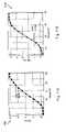
- FIG. 1shows a cross-sectional view of a memory device
- FIGS. 2-3show cross-sectional views of a gate stack of a memory device according to two embodiments
- FIGS. 4A-4Bare schematics showing the energy barrier to electron tunneling posed by dielectric layers according to several embodiments
- FIGS. 5-6show cross-sectional views of a gate stack of a memory device according to other embodiments.
- FIG. 7shows a contiguous charge storage layer according to one embodiment
- FIG. 8shows a non-contiguous charge storage layer according to another embodiment
- FIGS. 9A and 9Bshow simulation plots related to a combination control dielectric layer, according to various embodiments.
- FIGS. 10A-10C and 11 A- 11 Dshow plots related to a program/erase window for various gate stacks having one or more charge blocking layers, according to various embodiments
- FIGS. 11E and 11Fshow plots related to charge retention for memory devices including various exemplary gates stacks
- FIG. 12shows a cross-sectional view of a gate stack of a memory device according to another embodiment
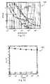
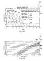
- FIG. 13shows a plot of erase time (x-axis) versus flat-band voltage (y-axis) for gate stacks using a nitride layer as the charge trapping layer, comparing a gate stack without one or more charge blocking layers and an improved gate stack with a charge blocking layer;
- FIG. 14shows a plot of the number of program and erase cycles (x-axis) versus the flat-band voltage (y-axis) using the improved gate stack of FIG. 13 ;
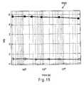
- FIG. 15shows a chart of room temperature charge retention mapping time (x-axis) versus flat-band voltage (y-axis) using the improved gate stack of FIG. 13 .
- FIG. 16A-16Bshow simulation plots related to a combination control dielectric layer, according to several embodiments.
- FIGS. 17A-17Cshow simulation plots related to a charge blocking layer having a composition gradient, according to several embodiments.
- FIG. 18shows a simulation plot related to a charge blocking layer having a composition gradient, according to several embodiments.
- FIGS. 19A-19Dshow simulation plots related to a charge blocking layer having a composition gradient, according to several embodiments.
- FIG. 20shows a flowchart of a method for forming an electronic device, such as a memory device, according to one embodiment
- FIG. 21is a cross-sectional view of an alternative embodiment of a gate stack of a memory device including a multilayer control dielectric
- FIGS. 22A-22Bare capacitance-voltage curves obtained from programming and erase operations on an embodiment of the gate stack of FIG. 21 where the high-k dielectric layers are 4 nm of HfO 2 ;
- FIGS. 23A-23Bare capacitance-voltage curves obtained from programming and erase operations on an embodiment of the gate stack of FIG. 21 where the high-k dielectric layers are 2 nm of HfO 2 ;
- FIGS. 24A-24Bare capacitance-voltage curves obtained from charge retention tests of an embodiment of the gate stack of FIG. 21 where the high-k dielectric layers are 4 nm of HfO 2 ;
- FIGS. 25A-25Bare capacitance-voltage curves obtained from charge retention tests of an embodiment of the gate stack of FIG. 21 where high-k dielectric layers are 2 nm of HfO 2 ;
- FIG. 26shows charge retention of an embodiment of the gate stack of FIG. 21 over time for both programming (upper data set) and erase (lower data set) states where the high-k dielectric layers are 2 nm of HfO 2 ;
- FIG. 27is a cross-sectional view of an alternative embodiment of a gate stack of a memory device including a multilayer control dielectric.
- FIG. 28is a cross-sectional view of an alternative embodiment of the gate stack of FIG. 21 .
- adjacentAs used herein to describe the relationship of one layer to another layer, are intended to be interpreted broadly to include layers in direct contact with one another and layers spaced apart by one or more intervening layers. Similarly, the term “between” is intended to be interpreted broadly to include a layer that is directly between two other layers or spaced apart from two other layers but still intermediate the two other layers.
- Embodiments of the present inventionare provided in the following sub-sections for electronic devices, such as non-volatile memory devices, including flash memory devices. Furthermore, embodiments for enhanced memory devices, such as multistate memory devices, are described. These embodiments are provided for illustrative purposes, and are not limiting. The embodiments described herein may be combined in any manner. Additional operational and structural embodiments will be apparent to persons skilled in the relevant art(s) from the description herein. These additional embodiments are within the scope and spirit of the present invention.
- a conventional charge storage layer memory cell or structureis programmed by applying appropriate voltages to the source, drain, and control gate nodes of the memory structure for an appropriate time period. Electrons are thereby caused to tunnel or be injected (e.g., via channel hot electrons) from a channel region to a charge storage layer, which is thereby “charged.” The charge stored in the charge storage layer sets the memory transistor to a logical “1” or “0.” Depending on whether the memory structure includes an enhancement or depletion transistor structure, when the charge storage layer is positively charged or contains electrons (negative charge), the memory cell will or will not conduct during a read operation.
- Erasingis the process of transferring electrons from the charge storage layer (or holes to the charge storage layer) (i.e., charge trapping layer).
- Programmingis the process of transferring electrons onto the charge storage layer.
- nonvolatile memory devicesusing metal or semiconductor nanocrystals (such as colloidal quantum dots or quantum dots formed using processes such as chemical vapor deposition or physical vapor deposition) or nonconductive nitride based charge trapping layers embedded in a high-k dielectric matrix, may be important to overcome the scaling limitations of conventional non-volatile memories beyond the 50 nm technology node and to fully enable reliable multi-bit operation.
- metal or semiconductor nanocrystalssuch as colloidal quantum dots or quantum dots formed using processes such as chemical vapor deposition or physical vapor deposition
- nonconductive nitride based charge trapping layers embedded in a high-k dielectric matrixmay be important to overcome the scaling limitations of conventional non-volatile memories beyond the 50 nm technology node and to fully enable reliable multi-bit operation.
- FIG. 1shows a detailed cross-sectional view of a memory device 100 , according to an exemplary embodiment.
- memory device 100is formed on a substrate 102 .
- Memory device 100includes source region 112 , channel region 114 , drain region 116 , a control gate or gate contact 118 , a gate stack 120 , a source contact 104 , a drain contact 106 .
- Source region 112 , channel region 114 , and drain region 116are configured generally similar to a transistor configuration.
- Gate stack 120is formed on channel region 114 .
- Gate contact 118which may alternatively be referred to as a control gate or gate electrode, is formed on gate stack 120 .
- Memory device 100generally operates as described above for conventional memories having charge storage layers.
- charge storage layer memory device 100includes gate stack 120 .
- Gate stack 120provides a charge storage layer for memory device 100 , and further features, as further described below.
- Gate stack 120may include any type of charge storage layer or charge storage medium. Exemplary charge storage layers are described below.
- substrate 102is a semiconductor type substrate, and is formed to have either P-type or N-type conductivity, at least in channel region 114 .
- Gate contact 118 , source contact 104 , and drain contact 106provide electrical connectivity to memory device 100 .
- Source contact 104is formed in contact with source region 112 .
- Drain contact 106is formed in contact with drain region 116 .
- Source and drain regions 112 and 116are typically doped regions of substrate 102 that have a conductivity different from that of channel region 114 .
- source contact 104is coupled to a potential, such as a ground potential.
- Drain contact 106is coupled to another signal. Note that source and drain regions 112 and 116 are interchangeable, and their interconnections may be reversed.
- FIG. 2shows a cross-sectional view of gate stack 120 , according to one exemplary embodiment.
- gate stack 120includes a tunneling dielectric layer 202 , a charge storage layer 204 , a charge blocking layer 206 , and a control dielectric layer 208 .
- tunneling dielectric layer 202is formed on channel region 114 of substrate 102 of memory device 100 .
- Charge storage layer 204is formed on tunneling dielectric layer 202 .
- Charge blocking layer 206is formed on charge storage layer 204 .
- Control dielectric layer 208is formed on charge blocking layer 206 .
- gate contact 118is formed on control dielectric layer 208 .
- the charge blocking layer 206may be formed on the control dielectric layer 208
- the gate contact 118may be formed on the charge blocking layer 206 , as shown in FIG. 11 .
- one or more further layers of materialmay separate the layers of gate stack 120 and/or may separate gate stack 120 from substrate 102 and/or gate contact 118 .
- Charge storage layer 204stores a positive or negative charge to indicate a programmed state of memory device 100 , as described above.
- Charge storage layer 204may include the materials described above, or otherwise known.
- a voltage applied to gate contact 118creates an electric field that causes electrons to tunnel (e.g., or via hot electron injection) into charge storage layer 204 from channel region 114 through tunneling dielectric layer 202 .
- the resulting negative charge stored in charge storage layer 204shifts a threshold voltage of memory device 100 . The charge remains in charge storage layer 204 even after the voltage is removed from gate contact 118 .
- an oppositely charged voltagemay be applied to gate contact 118 to cause electrons to discharge from charge storage layer 204 to substrate 102 through tunneling dielectric layer 202 or draws holes from the channel 114 to tunnel through (or via channel hot holes) the tunnel dielectric layer 202 to the charge storage layer 204 .
- Control dielectric layer 208isolates the gate contact 118 from the charge blocking layer 206 .
- the gate contact 118is preferably formed of a conductive material.
- the gate contact 118may be formed of polycrystalline silicon (polysilicon).
- the gate contact 118may be formed of a metal or a material including one or more metals, such as, for example, one or more transition metals.
- Exemplary transition metals that may be suitable for the gate contact 118include, but are not limited to: Ti, V, Cr, Mn, Fe, Co, Ni, Cu, Zn, Zr, Nb, Mo, Ru, Rh, Pd, Ag, Cd, Hf, Ta, W, Re, Os, Ir, Pt, Au, and Hg.
- the gate contact 118may be formed of TaN.
- the thickness of the gate contact 118is in the range of from about 5 nm to about 5,000 nm. Preferably, the thickness is in the range of from about 10 nm to about 500 nm.
- the gate contact 118may include a plurality of sublayers. Each sublayer may be formed of a different conductive material.
- the gate contact 118may be formed by vapor deposition techniques known in the art. Physical vapor deposition (PVD) techniques, such as sputtering or thermal evaporation, chemical vapor deposition (CVD), or atomic layer deposition (ALD) may be suitable for deposition of the gate contact 118 .
- PVDphysical vapor deposition
- CVDchemical vapor deposition
- ALDatomic layer deposition
- the charge storage layer 204may include any type of charge storage medium.
- the charge storage layer 204is a localized charge storage layer that includes a plurality of discrete charge storage elements.
- the discrete charge storage elementsmay be one or more localized charge traps, such as those found in a nitride layer, or semiconducting, metallic, or dielectric nanoparticles (quantum dots).
- charge storage layer 204may include nanocrystals formed of a high work function (e.g., greater than 4.5 eV) metal such as ruthenium (Ru), and preferably having a size of less than about 5 nm.
- a high work functione.g., greater than 4.5 eV
- Ruruthenium
- Such nanocrystalsmay be deposited on tunneling dielectric layer 202 by a variety of processes, such as chemical vapor deposition (CVD), atomic layer deposition (ALD) or physical vapor deposition (PVD), as is known in the art.
- Charge storage layer 204may also include preformed colloidal metal or semiconductor or dielectric quantum dots (nanocrystals) deposited on tunneling dielectric layer 202 .
- such materialsmay be deposited by methods such as spin coating, spray coating, printing, chemical assembly, nano-imprints using polymer self-assembly and the like, such as described in U.S. Pat. No. 6,586,785, U.S. application Ser. No. 11/147,670, and U.S. application Ser. No.
- Charge storage layer 204may also include a contiguous metal or semiconductor conductive layer, a non-contiguous metal or semiconductor conductive layer, a nonconductive nitride-based or other types of insulating charge trapping layer, a nonconductive oxide layer (e.g., SiO 2 ) having conductive elements disposed therein (e.g., silicon islands), a doped oxide layer, etc.
- a nonconductive oxide layere.g., SiO 2
- the charge storage layermay have a U-shape when viewed in cross-section along a word line direction of the memory cell.
- tunneling dielectric layer 202may be altered in order to provide an improved barrier to metal migration when metal quantum dots such as ruthenium (or other metal or alloy) are used for the charge storage material.
- gate stack 120 ′may include a barrier layer 302 formed on tunneling dielectric layer 202 between tunneling dielectric layer 202 and charge storage layer 204 .
- Barrier layer 302can include, for example, a nitrogen containing compound such as nitride (Si 3 N 4 ) or silicon oxynitride (SiO x N y , wherein x and y are positive numbers, 0.8, 1.5, etc., or other suitable barrier layer such as alumina (Al 2 O 3 ). Barrier layer 302 changes the surface structure of tunneling dielectric layer 202 such that metal migration effects may be minimized. Where barrier layer 302 is made from a nitrogen compound, the nitrogen-containing layer may be formed by adding nitrogen or a “nitrogen-containing” compound (e.g., “nitriding”) to tunneling dielectric layer 202 (e.g., which may be SiO 2 ).
- a nitrogen containing compoundsuch as nitride (Si 3 N 4 ) or silicon oxynitride (SiO x N y , wherein x and y are positive numbers, 0.8, 1.5, etc.
- barrier layer 302changes the surface structure of tunneling
- the nitrogen or nitrogen-containing compoundmay be deposited on tunneling dielectric layer 202 using a chemical vapor deposition (CVD) process, such as low pressure CVD (LPCVD) or ultra high vacuum CVD (UHVCVD).
- CVDchemical vapor deposition
- LPCVDlow pressure CVD
- UHVCVDultra high vacuum CVD
- the nitrogen-containing layermay be in direct contact with tunneling dielectric layer 202 .
- UHVCVD of barrier layer 302may be more controllable than LPCVD, as the UHVCVD generally occurs more slowly, and therefore the growth rate may be more closely regulated.
- the nitrogen-containing layermay be formed as a result of deposition from the reaction of such gases as silane (or other silicon source precursor such as dichlorosilane, or disilane) and ammonia (or other nitrogen species such as plasma-ionized nitrogen, N 2 O or NO), or a surface reaction to a reacting gas such as ammonia (or other nitrogen species such as plasma-ionized nitrogen, N 2 O or NO).
- Dichlorosilane and ammonia gas in combination with a co-flow of some inert gas and oxygen-containing gasmay be used for growth of the nitrogen-containing layer.
- Barrier layer 302impedes penetration of metal nanoparticles/quantum dots of charge storage layer 204 into tunneling dielectric layer 202 , such that contamination of tunnel dielectric layer 202 , which may result in leakage, is avoided.
- a thickness of barrier layer 302is preferably configured to ensure that carrier traps included in nitride structures do not dominate the charge storage aspects of the semiconductor device being formed.
- a desired thickness for barrier layer 302is less than about 10 angstroms. In further embodiments, the desired thickness may be about 5 angstroms or less.
- the relative thicknesses of tunneling dielectric layer 202 and barrier layer 302can be tailored to optimize electrical performance and metal migration barrier functions.
- the thickness of barrier layer 302should be at least that required to ensure generally uniform coverage of tunneling dielectric layer 202 by barrier layer 302 .
- the barrier layer 302is at least about 1 angstrom in thickness.
- the concentration of nitrogen within the silicon oxynitridemay be greater than about 5%, for example.
- a percentage concentration of nitrogen included in the silicon oxynitridecan be controlled such that the trade-off between the barrier function of the nitrogen layer against metal migration from metal quantum dots (when in charge storage layer 204 ) and the inclusion of traps due to nitride concentration is regulated.
- the tunneling dielectric layer 202is SiO 2 and the substrate 102 is silicon.
- the control dielectric layer 208may be formed of a single component oxide, such as, for example, Al 2 O 3 or SiO 2 . It is believed that SiO 2 may be advantageous as the control dielectric layer 208 because it poses a high energy barrier to electron tunneling (e.g., see FIG. 4B ). Also, SiO 2 contains few charge traps, and it is believed that those present in the layer are sufficiently deep that they do not hamper the charge retention of the device.
- the control dielectric layer 208may be formed of a multicomponent material such as a multicomponent oxide. According to one embodiment, the multicomponent oxide may be a silicate.
- Exemplary silicatesinclude Hf x Si 1-x O y , Al x Si 1-x O y , Zr x Si 1-x O y , and Hf x Al y Si z O, where x is a positive number between 0 and 1, and y and z are positive numbers.
- control dielectric layer 208have a thickness of no more than about 20 nm.
- the thickness of the control dielectric layeris believed to be important due to the scaling of new generations of memory devices to smaller lateral dimensions. As the channel length and device width of a memory cell reduce to below about 30 nm, it is desirable to reduce the thickness of the dielectric layer to less than the channel length such that the control gate can maintain the coupling to the charge storage layer.
- the control dielectric layer 208is about 15 nm or less in thickness.
- the control dielectric layer 208may also be about 10 nm or less in thickness. According to a preferred embodiment, the control dielectric layer 208 has a thickness of about 5 nm or less.
- control dielectric layer 208may be about 4 nm or less in thickness, about 3 nm or less in thickness, about 2 nm or less in thickness, or about 1 nm or less in thickness. It is also preferred that the thickness of the control dielectric layer 208 is at least that required to ensure generally uniform coverage of the underlying layer. Accordingly, the thickness of the control dielectric layer 208 is preferably at least about 0.1 nm.
- the thickness of the control dielectric layer 208is no more than about 200% of a thickness of the charge blocking layer 206 . More preferably, the thickness of the control dielectric layer 208 is no more than about 150% of the thickness of the charge blocking layer 206 .
- the thickness of the charge blocking layer 206is about 4 nm, and the thickness of the control dielectric layer 208 is about 5 nm or about 125% of the thickness of the charge blocking layer 206 .
- the thickness of the control dielectric layer 208is no more than about 125% of the thickness of the charge blocking layer 206 , or no more than about 100% of the thickness of the charge blocking layer 206 . It is also contemplated that the thickness of the control dielectric layer 208 may be less than the thickness of the charge blocking layer 206 .
- charge blocking layer 206is formed of a high-k dielectric material.
- a high-k dielectric materialhas a dielectric constant higher than that of SiO 2 (e.g., 3.9).
- the high-k dielectric material of the charge blocking layer 206may be, for example, Al 2 O 3 , HfO 2 , HfSiO 2 , ZrO 2 , Hf 1-x Al x O y , where x is a positive number between 0 and 1, and y is a positive number, e.g., HfAlO 3 , etc., preferably HfO 2 or Hf 1-x Al x O y , where x is a positive number between 0 and 1, and y is a positive number, e.g., HfAlO 3 .
- charge blocking layer 206may be formed of other high-k dielectric materials, such as Gd 2 O 3 , Yb 2 O 3 , Dy 2 O 3 , Nb 2 O 5 , Y 2 O 3 , La 2 O 3 , ZrO 2 , TiO 2 , Ta 2 O 5 , SrTiO 3 , Ba x Sr 1-x TiO 3 , Zr x Si 1-x O y , Hf x Si 1-x O y , Al x Zr 1-x O 2 , or Pr 2 O, for example.
- charge blocking layer 206has a higher dielectric constant than control dielectric layer 208 .
- control dielectric layer 208is Al 2 O 3 , which has a dielectric constant of approximately 9, and charge blocking layer 206 is HfO 2 , which has a dielectric constant of less than about 25, e.g., around 22, when deposited.
- control dielectric layer 208is SiO 2 , which has a dielectric constant of approximately 4, while charge blocking layer is HfO 2 .
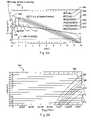
- FIGS. 4A-4Cinclude plots 400 , 410 , 420 showing schematically how including a dielectric layer of a higher dielectric constant (e.g., the charge blocking layer 206 ) adjacent to a dielectric layer of a lower dielectric constant (e.g., the control dielectric layer 208 ) may improve tunneling resistance.
- the plot 400 of FIG. 4Ashows the energy barrier (eV) of a dielectric layer having a higher dielectric constant (e.g., HfO 2 ) alone
- the plot 410 of FIG. 4Bshows the energy barrier of a dielectric layer having a lower dielectric constant (e.g., SiO 2 ) alone.
- the lower k-dielectric layer (SiO 2 )provides a higher energy barrier to tunneling than does the higher-k dielectric layer (HfO 2 ), but the higher-k dielectric layer (HfO 2 ) provides a wider barrier.
- the plot 420 of FIG. 4Cshows the improvement in the magnitude of the tunneling barrier when the higher-k dielectric layer (e.g., HfO 2 ) is disposed adjacent to the lower-k dielectric layer (e.g., SiO 2 ). Accordingly, tunneling current may be reduced.
- Any combination of higher-k and lower-k dielectricsmay be suitable for the charge blocking layer 206 and the control dielectric layer 208 .
- the charge blocking layer 206has the higher dielectric constant (e.g., lower barrier height)
- the control dielectric layer 208has the lower dielectric constant (e.g., higher barrier height).
- charge blocking layer 206may include a gradient of composition, band gap value and/or dielectric constant through a thickness of the layer 206 .
- the gradientmay increase or decrease from a first surface of charge blocking layer 206 (e.g., a surface of charge blocking layer 206 adjacent to charge storage layer 204 ) to a second surface of charge blocking layer 206 (e.g., a surface of charge blocking layer 206 adjacent to control dielectric layer 208 ).
- the charge blocking layer 206 having a gradient of compositionmay comprise a dielectric material, and an amount of at least one component of the dielectric material may vary across the thickness of the charge blocking layer 206 .
- the dielectric materialis a high-k dielectric material.
- the amount of the componentmay vary linearly, nonlinearly, or step-wise across the thickness of the charge blocking layer 206 .
- the amount of the componentis a minimum near the control dielectric layer 208 and increases across the thickness of the charge blocking layer 206 .
- the componentmay be an element or a compound.
- the componentmay be hafnium or hafnium oxide.
- the charge blocking layer 206 having a gradient of compositionis formed of a multicomponent dielectric material.
- the charge blocking layer 206may be formed of a multicomponent oxide such as, Hf x Al 1-x O y , Hf x Si 1-x O y , Zr x Si 1-x O y , Ba x Sr 1-x TiO y , or Al x Zr 1-x O y .
- the multicomponent dielectric materialmay include the component (e.g., hafnium) and a second component, and a ratio of the component to the second component may vary across the thickness of the charge blocking layer 206 , according to an exemplary embodiment.
- the multicomponent dielectric materialmay include nitrogen.
- the multicomponent dielectric materialmay be Hf x Si 1-x O 2-y N y , according to an exemplary embodiment.
- the charge blocking layer 206 having a gradient of compositionmay be disposed between the charge storage layer 204 and the control dielectric layer 208 , or between the control dielectric layer 208 and the gate contact 118 of the memory device 100 .
- charge blocking layer 206comprises a plurality of layers of materials.
- FIG. 5shows, for example, a charge blocking layer 206 including three layers.
- the charge blocking layer 206includes a first layer 210 closest to the charge storage layer 204 , a second (middle) layer 212 , and a third layer 214 (furthest from the charge storage layer 204 ).
- the layer closest to charge storage layer 204is formed of a relatively high band gap material, while the layer(s) further from charge storage layer 204 are formed of material(s) having a progressively lower band gap.
- charge storage layer 204comprises isolated particles (e.g., nanoparticles, quantum dots), because a relatively higher band gap material allows less tunneling between particles than a lower band gap material.
- SiO 2 , Al 2 O 3 , HfAlO 3are exemplary materials having relatively high band gap.
- an alternative embodimentwould include a layer closest to the charge storage layer 204 being formed of a relatively low band gap material, and layer(s) further from the charge storage layer 204 being formed of material(s) having a progressively higher band gap.
- the first layer 210may be Al 2 O 3
- the second (middle) layer 212may be HfAlO 3
- the third layer 214may be HfO 2 (which has a relatively low band gap).
- the first layer(closest to charge storage layer 204 ) may be SiO 2
- the second layermay be HfO 2 , which has a relatively high dielectric constant (for effective charge blocking) and a low band gap.
- control dielectric layer 208may be a material such as Al 2 O 3 or SiO 2 .
- charge blocking layer 206may be doped.
- charge blocking layer 206may be doped with dopant materials, such as a rare earth metal, transition metal, silicon, oxygen, or nitrogen.
- the charge blocking layer 206may be Hf 1-x Si x O 2-y N y .
- the nitrogenmay be introduced by a post deposition nitridation treatment.
- a Hf 1-x Si x O 2 layermay be annealed in an environment containing NH 3 , N 2 O, or NO to form the Hf 1-x Si x O 2-y N y layer.
- charge blocking layer 206is formed to be relatively thin, such as less than about 10 nm, e.g., less than about 5 nm, e.g., less than about 2 nm, to reduce trapping of electrons by the high dielectric material of charge blocking layer 206 .
- the charge blocking layer 206has a thickness sufficient to ensure generally uniform coverage of the underlying layer.
- the charge blocking layer 206may be at least 0.1 nm thick.
- the charge blocking layer 206is at least 0.5 nm thick.
- FIG. 6shows another cross-sectional view of gate stack 120 ′′, according to an exemplary embodiment.
- the configuration of gate stack 120 ′′ in FIG. 6is generally similar to FIG. 2 , except that in FIG. 6 , gate stack 120 ′′ further includes a second charge blocking layer 402 formed on control dielectric layer 208 .
- gate contact 118is formed on second charge blocking layer 402 .
- second charge blocking layer 402is formed of a high-k dielectric material, such as Al 2 O 3 , HfO 2 , ZrO 2 , Hf 1-x Al x O y , where x is a positive number between 0 and 1, and y is a positive number, e.g., HfAlO 3 , Hf 1-x Si x O 2 , Hf 1-x Si x O 2-y N y , etc., preferably HfO 2 .
- the second charge blocking layer 402may be formed of any of the materials described above for first charge blocking layer 206 , and may be configured similarly, such as in a single layer configuration (uniform or gradient of material) or multi-layer configuration.
- the second charge blocking layer 402may comprise a dielectric material, and an amount of at least one component of the dielectric material may vary across the thickness of the charge blocking layer 402 .
- the dielectric materialis a high-k dielectric material.
- the amount of the componentmay vary linearly, nonlinearly, or step-wise across the thickness of the second charge blocking layer 402 .
- the amount of the componentis a minimum near the control dielectric layer 208 and increases across the thickness of the second charge blocking layer 402 .
- the componentmay be an element or compound.
- the componentmay be hafnium or hafnium oxide.
- the second charge blocking layer 402 having a gradient of compositionis formed of a multicomponent dielectric material.
- the second charge blocking layer 402may be formed of a multicomponent oxide such as, Hf x Al 1-x O y , Hf x Si 1-x O y , Zr x Si 1-x O y , Ba x Sr 1-x TiO y , or Al x Zr 1-x O y .
- the multicomponent dielectric materialmay include the component (e.g., Hf) and a second component, and a ratio of the component to the second component may vary across the thickness of the second charge blocking layer 402 , according to an exemplary embodiment.
- the multicomponent dielectric materialmay include nitrogen.
- the multicomponent dielectric materialmay be Hf x Si 1-x O 2-y N y , according to an exemplary embodiment.
- the second charge blocking layer 402 having a gradient of compositionmay be disposed between the control dielectric layer 208 and the gate contact 118 of the memory device 100 , or between the charge storage layer 204 and the control dielectric layer 208 .
- Charge blocking layers 206 and 402may efficiently block charge transport through control dielectric layer 208 .
- first charge blocking layer 206e.g., HfO 2
- Second charge blocking layer 402e.g., HfO 2
- the first and/or second charge blocking layers 206 , 402may have other functions.
- the thicknesses of first and second charge blocking layers 206 and 402are thin, such as less than 10 nm, e.g., less than 5 nm.
- first and second charge blocking layer 206 and 402Another advantage of the first and second charge blocking layer 206 and 402 is that, although high-k dielectric layers can themselves have traps, first and second charge blocking layers 206 and 402 can be made very thin, such as less than about 4 nm, e.g., less than 2 nm, to reduce a total amount of charge traps while efficiently blocking current flow. Furthermore, second charge blocking layer 402 is positioned adjacent to gate contact 118 . Thus, even if a relatively large amount of charge is trapped in second charge blocking layer 402 , an effect on the flat-band voltage is proportional to a distance from second charge blocking layer 402 to gate contact 118 , which is minimal (since they may be directly adjacent to (in contact with) each other).
- first and second charge blocking layers 206 and 402are HfO 2
- control dielectric layer 208is Al 2 O 3
- a program/erase (P/E) windowis the voltage difference between threshold states of a program state and an erase state.
- memory device 100can be erased (e.g., up to ⁇ 6V), with a P/E window of 12.8V or greater.
- the P/E windowmay range from about 8 V to about 16 V (e.g., in ranges of from about 9 V to about 14V, about 10 V to about 13V, or have values of about 9 V, about 10 V, about 11V, about 12V, or about 13V).
- the P/E windowmay be as large as 14.2V, approaching multi-state memory voltage requirements, such as for 3-bit or even 4-bit memory cells;
- the P/E windowmay not show significant drift after 100,000 P/E cycles.
- Chargemay be retained in charge storage layer 204 at a 12V P/E window, and more importantly 100,000 P/E cycles may not degrade the charge retention characteristics.
- the control dielectric layermay have a multilayer structure including two or more sublayers.
- the control dielectric layer 2208may include three sublayers.
- FIG. 21shows an exemplary gate stack 2120 of a memory device that includes a tunneling dielectric layer 202 , a charge storage layer 204 comprising localized charge traps or a continuous floating gate, a first charge blocking layer 206 , a control dielectric layer 2208 including three sublayers 2102 , 2104 , 2106 , and a second charge blocking layer 402 overlying the control dielectric layer 2208 .
- Deposition techniques known in the artsuch as chemical vapor deposition or atomic layer deposition, may be employed to form the control dielectric layer 2208 having the sublayer structure.
- the control dielectric layer 2208may have an ONO structure including a first oxide layer 2102 , a nitride layer 2104 overlying the oxide layer 2102 , and a second oxide layer 2106 .
- the first oxide layer 2102may be SiO 2
- the nitride layer 2104may be SiN
- the second oxide layer 2106may be SiO 2 .
- the thickness of each sublayer of the control dielectric layer 2208is preferably about 4 nm or less, and more preferably about 3 nm or less.
- the ONO layersmay have the structure: SiO 2 (3 nm)/SiN (3 nm)/SiO 2 (3 nm).
- a control dielectric layer 2208 having such a sublayer structurehas been shown to be effective in combination with hafnium-based charge blocking layers 206 , 402 and a nanodot charge storage layer 204 in providing a gate stack 2120 with excellent charge retention capabilities and program/erase characteristics.
- the control dielectric layermay also be effective in combination with a nitride trap storage layer and one or more charge blocking layers, as will be discussed further below.
- the physical layer thickness of the gate stackmay be reduced for the same EOT when ONO layers are employed as the control dielectric layer instead of a single aluminum oxide layer, for example. Another advantage of using ONO layers is that they may be readily etched without damaging the sidewalls of the gate stack.
- FIGS. 22A and 22Bshow program and erase characteristics, respectively, for a gate stack (“gate stack A”) including an 8 nm SiO 2 tunneling dielectric layer 202 , Ru nanocrystals as the charge storage layer 204 , a 4 nm hafnium oxide layer as the first charge blocking layer 206 , an ONO stack of SiO 2 (3 nm)/SiN (3 nm)/SiO 2 (3 nm) as the control dielectric layer 2208 , and a 4 nm hafnium oxide layer as the second charge blocking layer 402 .
- gate stack Aincluding an 8 nm SiO 2 tunneling dielectric layer 202 , Ru nanocrystals as the charge storage layer 204 , a 4 nm hafnium oxide layer as the first charge blocking layer 206 , an ONO stack of SiO 2 (3 nm)/SiN (3 nm)/SiO 2 (3 nm) as the control dielectric layer 2208 , and a 4 n
- Each capacitance versus voltage (C-V) curverepresents a shift of ⁇ 1V in gate voltage compared to the previous curve, for a ⁇ 12V to ⁇ 22V sweep, with capacitance given in farads.
- a 1V step sizewhich is nearly achieved during the programming operation, may be obtained with ideal charge blocking behavior.
- FIGS. 23A and 23Bshow program and erase characteristics, respectively, for a gate stack (“gate stack B”) including an 8 nm SiO 2 tunneling dielectric layer 202 , Ru nanocrystals as the charge storage layer 204 , a 2 nm hafnium oxide layer as the first charge blocking layer 206 , an ONO stack of SiO 2 (3 nm)/SiN (3 nm)/SiO 2 (3 nm) as the control dielectric layer 2208 , and a 2 nm hafnium oxide layer as the second charge blocking layer 402 .
- gate stack Bincluding an 8 nm SiO 2 tunneling dielectric layer 202 , Ru nanocrystals as the charge storage layer 204 , a 2 nm hafnium oxide layer as the first charge blocking layer 206 , an ONO stack of SiO 2 (3 nm)/SiN (3 nm)/SiO 2 (3 nm) as the control dielectric layer 2208 , and a 2 n
- each C-V curverepresents a shift of ⁇ 1V in gate voltage for a ⁇ 12V to ⁇ 22V sweep, and capacitance is shown in farads. A roughly 1V step size between the curves is attained during the programming operation.
- FIGS. 24A-24Bshow charge retention characteristics for gate stack A immediately after programming ( FIG. 24A ) and erase ( FIG. 24B ) operations at 250° C., and then after 1 min, 10 min, and 60 min. These test conditions were employed to simulate charge retention over a much longer period (e.g., up to ten years) at room temperature.
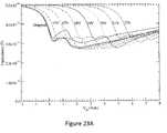
- FIGS. 25A-25Bshow charge retention characteristics for gate stack B under the same conditions after programming ( FIG. 25A ) and erase ( FIG. 25B ) operations.
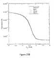
- the charge retention of gate stack B at 250° C.is shown as a function of time in FIG. 26 .
- the change in the flat band voltage ( ⁇ V FB )is less than 0.1 V after 60 minutes at 250° C.
- the control dielectric layermay 2208 may be part of a gate stack including a nitride trap (e.g., SiN) charge storage layer.
- FIG. 27shows an exemplary gate stack 2720 of a memory device that includes a tunneling dielectric layer 202 , a nitride charge storage layer 204 including localized charge traps, the control dielectric layer 2208 including three sublayers 2102 , 2104 , 2106 , and a charge blocking layer 206 overlying the control dielectric layer.
- a nitride trape.g., SiN
- the control dielectric layer 2208may have an ONO structure including a first oxide layer 2102 , a nitride layer 2104 overlying the oxide layer 2102 , and a second oxide layer 2106 .
- the first oxide layer 2102may be SiO 2
- the nitride layer 2104may be SiN
- the second oxide layer 2106may be SiO 2 .
- the thickness of each sublayer of the control dielectric layer 2208is preferably about 4 nm or less, and more preferably about 3 nm or less.
- the ONO layersmay have the structure: SiO 2 (3 nm)/SiN (3 nm)/SiO 2 (3 nm).
- the control dielectric layer 2208 of the exemplary gate stacks 2120 , 2720 of FIGS. 21 and 27is not limited to an ONO stack.
- the control dielectric layer 2208may include, for example, one or more silicate layers, such as Hf x Si 1-x O y , Al x Si 1-x O y , Zr x Si 1-x O y , and Hf x Al y Si z O, where x is a positive number between 0 and 1, and y and z are positive numbers.
- the control dielectric layer 2208may include a central layer 2104 comprising a metal silicate sandwiched between two oxide layers 2102 , 2106 .
- control dielectric layer 2208may have the structure HfO 2 /HfSiO/HfO 2 .
- the control dielectric layer 2208may be comprised entirely of metal silicate sublayers 2102 , 2104 , 2106 , such as HfSiO/AlSiO/HfSiO.
- the charge blocking layer 206 of FIG. 27 , and each of the first and second charge blocking layers 206 , 402 of FIG. 21 ,are preferably formed of a high-k dielectric material.
- the high-k dielectric materialmay be a single component oxide such as HfO 2 .
- the high-k dielectric materialmay be a multicomponent oxide such as a metal silicate (e.g., hafnium silicate or aluminum silicate).
- Suitable materials for the first and second charge blocking layersmay include: Al 2 O 3 , HfO 2 , ZrO 2 , Gd 2 O 3 , Yb 2 O 3 , Dy 2 O 3 , Nb 2 O 5 , Y 2 O 3 , La 2 O 3 , ZrO 2 , TiO 2 , Ta 2 O 5 , Pr 2 O, SrTiO 3 , Ba x Sr 1-x TiO 3 , Zr x Si 1-x O y , Hf x Si 1-x O y (e.g., HfSiO 4 ), Hf 1-x Al x O y , (e.g., HfAlO 3 ), Al x Si 1-x O y , Hf x Al y Si z O, and Al x Zr 1-x O y , where x is a positive number between 0 and 1, and y and z are positive numbers.
- the charge blocking layersmay include nitrogen and/or a gradient of composition across the thickness of the layer.
- the thickness of the first and second charge blocking layers 206 , 402is about 4 nm or less, or about 2 nm or less.
- the tunneling dielectric layer 202 of the gate stacks 2120 , 2720is as described previously, and may be SiO 2 .
- a thin dielectric layer 2210may lie between the control dielectric layer 2208 and the first charge blocking layer 206 and/or the second charge blocking layer 402 .
- the dipole momentdiffers with different combinations of dielectric materials.
- FIG. 28which shows an alternative embodiment 2120 ′ of the gate stack 2120 of FIG.
- a first thin dielectric layer 2210 amay be disposed between the first charge blocking layer 206 and the control dielectric layer 2208
- a second thin dielectric layer 2210 bmay be disposed between the second charge blocking layer 402 and the control dielectric layer 2208
- the thin dielectric layer(s) 2210has a thickness of about 1 nm or less. The thickness may also be about 0.5 nm or less.
- a very thin Al 2 O 3 layer of less than about 1 nm in thickness inserted at a HfO 2 and SiO 2 interfacemay be sufficient to increase the dipole moment.
- the tunnel barrier heightmay be increased and the leakage tunneling current may be suppressed.
- the program windowcan be improved due to the increased barrier height on top of the conductive charge storage elements (e.g., nanocrystals or a floating gate).
- the erase windowcan be improved due to increased barrier height for the control gate 118 during erase.
- other single-component or multi-component oxidesmay also be suitable, such as HfO 2 , ZrO 2 , Gd 2 O 3 , Yb 2 O 3 , Dy 2 O 3 , Nb 2 O 5 , Y 2 O 3 , La 2 O 3 , ZrO 2 , TiO 2 , Ta 2 O 5 , Pr 2 O, SrTiO 3 , Ba x Sr 1-x TiO 3 , Zr x Si 1-x O y , Hf x Si 1-x O y (e.g., HfSiO 4 ), Hf 1-x Al x O y , (e.g., HfAlO 3 ), Al x Si 1-x O y , Hf x Al y Si z
- charge storage layer 204is a single continuous region.
- FIG. 7shows a plan view of charge storage layer 204 having a planar, continuous configuration.
- charge storage layer 204may be formed from a continuous film of silicon (or polysilicon), a metal, etc. In such a configuration, if a single point of the continuous region breaks down and begins to lose charge, the entire region can lose its charge, causing memory device 100 to lose its programmed state.
- FIG. 8shows a plan view of charge storage layer 204 having a non-continuous configuration, according to an exemplary embodiment. In the example of FIG.
- charge storage layer 204comprises a plurality of nanoparticles 802 . Because nanoparticles 802 of charge storage layer 204 each separately store charge, and are insulated from one another, even if a single nanoparticle loses charge, this will not likely affect the remaining nanoparticles of charge storage layer 204 . The same advantage may be obtained with nonconductive nitride-based charge storage layers which store charge in localized charge trap regions. Thus, a memory device incorporating a charge storage layer 204 according to the present disclosure may maintain a constant programmed state over a much longer time than conventional memory devices.
- nanoparticles 802are electrically isolated nanocrystals.
- Nanocrystalsare small clusters or crystals of a conductive material that are electrically isolated from one another. Generally, nanocrystals have a crystallite size of approximately 100 nm or less.
- One advantage in using nanocrystals for charge storage layer 204is that they do not form a continuous film, and thus charge storage layers formed of nanocrystals are self-isolating. Because nanocrystals form a non-continuous film, charge storage layers may be formed without concern about shorting of the charge storage medium of one cell level to the charge storage medium of adjacent cells lying directly above or below (i.e., vertically adjacent). Yet another advantage of the use of nanocrystals for charge storage layers is that they may experience less charge leakage than do continuous film charge storage layers.
- Nanocrystalscan be formed from conductive material such as palladium (Pd), iridium (Ir), nickel (Ni), platinum (Pt), gold (Au), ruthenium (Ru), cobalt (Co), tungsten (W), tellurium (Te), rhenium (Re), molybdenum (Mo), iron platinum alloy (FePt), tantalum (Ta), tantalum nitride (TaN), etc.
- conductive materialsuch as palladium (Pd), iridium (Ir), nickel (Ni), platinum (Pt), gold (Au), ruthenium (Ru), cobalt (Co), tungsten (W), tellurium (Te), rhenium (Re), molybdenum (Mo), iron platinum alloy (FePt), tantalum (Ta), tantalum nitride (TaN), etc.
- Such materialsgenerally have a higher work function (e.g., about 4.5 eV or higher) than
- a metal nanocrystal charge storage layercan be formed by physical vapor deposition (PVD) or atomic layer deposition (ALD) in which a thin film is first deposited on a surface of a substrate (e.g., by sputtering using PVD) and then annealed at high temperature (e.g., about 900 degrees C. or higher) for a short time (e.g., about 10 seconds) to coalesce metal particles of nanoscale dimensions.
- PVDphysical vapor deposition
- ALDatomic layer deposition
- the uniformity and size of the metal particlescan be controlled by varying the thickness of the sputtered metal layer, the annealing temperature and annealing time, pressure, and ambient gas species, etc.
- the silicon nanocrystalsmay be formed by a process such as CVD as described, for example, in U.S. Pat. No. 6,297,095, which is incorporated by reference herein in its entirety.
- Charge storage layer 204may include preformed colloidal metal or semiconductor quantum dots deposited on the tunneling dielectric layer 202 by methods such as spin coating, spray coating, printing, chemical self-assembly and the like. For example, such processes are described in U.S. Pat. No. 6,586,785, U.S. application Ser. No. 11/147,670, and U.S. application Ser. No. 11/495,188, which is each incorporated by reference herein in its entirety.
- a nonconductive trapping layer formed in a dielectric stack of the gate stackmay be used.
- the charge storage mediumcan be a dielectric stack comprising a first oxide layer (e.g., tunneling dielectric layer 202 ) adjacent to channel region 114 , a nonconductive nitride layer adjacent to the first oxide layer, and a second oxide layer adjacent to the nitride layer and adjacent to gate contact 118 .
- a dielectric stackis sometimes referred to as an ONO stack (i.e., oxide-nitride-oxide) stack.
- the second oxide layercan be replaced with one of gate stacks 120 , 120 ′, or 120 ′′ to improve the performance of the traditional ONO stack.
- Other suitable charge trapping dielectric filmssuch as an H+ containing oxide film can be used if desired.
- charge storage layer 204includes metal dots
- charge blocking layer 206is HfO 2
- control dielectric layer 208is Al 2 O 3
- FIG. 9Ashows a simulation plot 900 of energy (eV) versus a thickness (nm) for a combination control dielectric of charge blocking layer 206 (HfO 2 ) and control dielectric layer 208 (Al 2 O 3 ).
- FIG. 9Bshows a simulation plot 920 of current (A/cm 2 ) versus electric field (V/cm). The plot includes a plot line 902 for the combination control dielectric including only HfO 2 , and a plot line 904 for the combination control dielectric including only Al 2 O 3 .
- FIGS. 9A and 9Bshow that including a thin layer of HfO 2 at the interface of metal and Al 2 O 3 can reduce the electron tunneling current by many orders of magnitude. This is true even if the HfO 2 layer is less than 1 nm thick.
- FIGS. 10A-10Cshow plots 1000 , 1010 , and 1020 related to an exemplary gate stack similar to gate stack 120 shown in FIG. 2 .
- an erase voltageis approximately ⁇ 3.7V and a program voltage is approximately 9.3V, for a total P/E window of 13 V.
- FIGS. 11A and 11Bshow plots 1100 , 1120 of program and erase voltages for an exemplary gate stack similar to gate stack 120 ′′ shown in FIG. 6 .
- charge storage layer 204is formed of quantum dots
- first charge blocking layer 206is formed of HfO 2 having a thickness of 4 nm
- control dielectric layer 208is formed of Al 2 O 3 at a thickness of 12 nm
- second charge blocking layer 402is formed of HfO 2 at a thickness of 4 nm.
- a P/E linear windowis approximately 11.39V.
- FIGS. 11C and 11Drespectively show plots 1130 and 1140 of program and erase voltages for an exemplary gate stack similar to gate stack 120 ′′ shown in FIG. 6 .
- charge storage layer 204is formed of quantum dots
- first charge blocking layer 206is formed of HfO 2 having a thickness of 4 nm
- control dielectric layer 208is formed of Al 2 O 3 at a thickness of 12 nm
- second charge blocking layer 402is formed of HfO 2 at a thickness of 8 nm.
- a P/E linear windowis approximately 12.76V.
- FIGS. 11E and 11Fshow plots 1150 and 1160 , respectively, obtained from charge retention tests of memory devices including four exemplary gate stacks similar to gate stack 120 ′′ shown in FIG. 6 .
- first charge blocking layer 206is formed of HfO 2 of 2 nm in thickness that has undergone a nitridation treatment
- control dielectric layer 208comprises Al 2 O 3 of 16 nm in thickness
- second charge blocking layer 402is formed of HfO 2 of 2 nm in thickness that has undergone a nitridation treatment.
- first charge blocking layer 206is formed of HfO 2 of 4 nm in thickness that has undergone a nitridation treatment
- control dielectric layer 208comprises Al 2 O 3 of 12 nm in thickness
- second charge blocking layer 402is formed of HfO 2 of 4 nm in thickness that has undergone a nitridation treatment.
- the nitridation treatmententails an ammonia (NH 3 ) anneal followed by a rapid thermal anneal (RTA) in nitrogen
- RTArapid thermal anneal
- the nitridation treatmententails just the RTA in nitrogen.
- the ammonia annealwas carried out at 900° C. for 1 h at an ammonia pressure of 250 mTorr, and the RTA was carried out in flowing nitrogen at 950° C. for 20 s.
- the nitridation treatmentmay be carried out in a nitrogen plasma. Having undergone the nitridation treatment, all or a portion of the first and second charge blocking layers 206 , 402 of the exemplary embodiments may include hafnium oxynitride (HfON).
- the sampleswere prepared on a substrate including an 80 ⁇ SiO 2 tunnel oxide layer.
- the charge storage layer 204 of the four exemplary gate stacks in the examples of FIGS. 11E and 11Fincludes metal nanocrystals, but alternatively the charge storage layer 204 may be a nitride layer or a polycrystalline silicon (polysilicon) layer, as described previously.
- a dual layer dielectric structureincluding just the first charge blocking layer 206 and the control dielectric layer 208 , as shown for example in FIGS. 2 and 12 , may be advantageous.
- the memory devices including the exemplary gate stacksare initially programmed to approximately 4V and then baked (heated) at 250° C. for up to 24 hours. Under these conditions, the memory devices undergo an accelerated reliability test that allows the charge loss that would occur over a much longer period (e.g., up to ten years) at room temperature to be simulated.
- FIG. 11Eshows flatband voltage V FB as a function of bake time in seconds, where data were obtained from each memory device at the start, after 60 seconds, after 600 seconds, and after 3,600 seconds (1 hour).
- the memory devices including the gate stacks that were nitrided in ammoniashow the best charge retention.
- the memory device including the gate stack having a 16 nm Al 2 O 3 layer sandwiched between two 2 nm HfO 2 layershad the higher charge retention with a charge loss ( ⁇ V FB ) of about 0.1 V at 250° C. for 1 h.
- the memory deviceincluding the 12 nm Al 2 O 3 layer sandwiched between two 4 nm HfO 2 layers (second embodiment of the gate stack; curve 1154 ) showed the second best charge retention with a charge loss of about 0.7 V at 250° C. for 1 h.
- the memory devices including the gate stacks that underwent only the RTA in nitrogenshow higher charge losses.
- the memory device including the gate stack having a 12 nm Al 2 O 3 layer sandwiched between two 4 nm HfO 2 layershad the lowest charge retention of all four devices with a charge loss of about 1 V at 250° C. for 1 h.
- the third embodiment of the gate stack(curve 1156 ), with a 16 nm Al 2 O 3 layer sandwiched between two 2 nm HfO 2 layers, exhibited a charge loss of about 0.8 V at 250° C. for 1 h.
- the charge retention of the memory device including the first embodiment of the gate stackwhich includes the 16 nm Al 2 O 3 layer sandwiched between two 2 nm HfO 2 layers that underwent the ammonia anneal and then the RTA, was evaluated over a 24 h period at the same test temperature of 250° C.
- the memory deviceexhibited a charge loss ( ⁇ V FB ) Of 0.32 V over the duration of the test.
- the memory deviceexhibits a charge loss of about 0.5 V or less over a period of 24 hours at 250° C.
- the memory devicepreferably exhibits a charge retention of about 85% or greater. More preferably, the memory device exhibits a charge retention of about 90% or greater.
- control dielectric layer 208has a thickness of from about 6 times to about 10 times that of the first and second charge blocking layers 206 , 402 .
- control dielectric layer 208may have a thickness of from about 4 nm to about 18 nm, or from about 8 nm to about 16 nm, and for each of the first and second charge blocking layers 206 , 402 to have a thickness of from about 1 nm to about 6 nm, or from about 1 nm to about 3 nm.
- the oxynitride layerswere formed by nitriding hafnium oxide layers deposited by atomic layer deposition or a similar technique. It is also contemplated that the oxynitride may include a component other than hafnium and may be formed by nitriding an oxide other than hafnium oxide.
- the oxynitridemay be a silicon oxynitride formed by nitriding silicon oxide.
- the oxynitridemay include a component M (MO 2-y N y ), where M is selected from the group consisting of, for example, Hf, Si, and Al.
- the oxynitridemay also include more than one component (e.g., M and M′) in addition to oxygen and hydrogen; for example, the component M may be present at a concentration x and M′ may be present at a concentration of 1-x: M x M′ 1-x O 2-y N y .
- Mmay be Hf and M′ may be Si
- the oxynitridemay be Hf x Si 1-x O 2-y N y .
- the second charge blocking layer 402may include an excess of nitrogen compared to the first charge blocking layer 206 . Accordingly, it may be advantageous to carry out a nitridation treatment after the first charge blocking layer 206 is deposited and before the second charge blocking layer 402 is deposited, and then to repeat the nitridation treatment after forming the second charge blocking layer 402 . Using this processing approach, the first and second charge blocking layers 208 , 402 may contain similar amounts of nitrogen.
- a layer of HfO 2may be deposited as the first charge blocking layer 206 on the charge storage layer 204 of the gate stack 120 ′′.
- the devicePrior to depositing additional layers, the device may be placed in a furnace and annealed in, for example, 250 mTorr of ammonia for 1 h at about 900° C.
- an oxynitride (HfON)may be formed from some or all of the oxide (HfO 2 ) of the first charge blocking layer 206 .
- control dielectric layer 208e.g., Al 2 O 3
- second charge blocking layer 402e.g., HfO 2
- the devicemay be returned to the furnace and annealed in ammonia for 1 h at 900° C. as described previously. Consequently, HfON may be obtained from some or all of the HfO 2 of the second charge blocking layer 402 , as well as from some or all of the first charge blocking layer 206 .
- RTArapid thermal anneal
- the ammonia annealis preferably carried out at a temperature of about 900° C. or less.
- the annealmay be carried out at a temperature of about 850° C. or less, or at a temperature of about 800° C. or less.
- the temperature of the ammonia annealis at least about 750° C.
- the duration of the ammonia annealis preferably about 60 minutes, although any time in the range of from about 50 minutes to about 70 minutes may be suitable for the nitridation treatment.
- a rapid thermal anneal in ammoniamay be carried out at higher temperatures and shorter times than a furnace anneal in ammonia.
- the gate stack of the memory devicemay include a nitride layer as the charge storage layer, an Al 2 O 3 layer as the control dielectric layer, and a hafnium containing compound such as HfO 2 as the charge blocking layer.
- the charge blocking layer 206may be formed above the control dielectric layer 208 and adjacent the control gate 118 according to this embodiment.
- the gate stackmay include one (or more) other charge blocking layers, such as a charge blocking layer below the control dielectric layer and adjacent the nitride layer.
- FIG. 13shows a chart 1300 of erase time (x-axis) versus flat-band voltage (y-axis) comparing a conventional gate stack (reference numeral 1304 ) without one (or more) charge blocking layers, versus an improved gate stack (reference numeral 1302 ) described above using a nitride layer as the charge trapping layer and a charge blocking layer (e.g., HfO 2 ) formed adjacent to the control dielectric layer (e.g., Al 2 O 3 ).
- FIG. 14shows a chart 1400 comparing the number of program and erase cycles (x-axis) versus the flat-band voltage (y-axis) using the improved gate stack represented by reference numeral 1302 in FIG. 13 .
- FIG. 14shows a chart of room temperature charge retention mapping time (x-axis) versus flat-band voltage (y-axis) using the improved gate stack.
- the use of the improved gate stack 1302 comprising charge blocking layer (e.g., HfO 2 ) formed over the control dielectric layer (e.g., Al 2 O 3 ) with a nitride charge trapping layershows an enhancement in the memory P/E window (e.g., on the order of about 2 volts or greater) compared to conventional gate stack 1304 including only an Al 2 O 3 control dielectric layer without a charge blocking layer.
- Such a memory device with the improved gate stackhas a total P/E window of greater than about 8 volts, which is believed to be the highest P/E window reported in the literature to date using a nitride layer as the charge trapping layer.
- the P/E windowdoes not show significant drift after 100,000 P/E cycles using the improved gate stack embodiment.
- the chargeis retained at greater than an 8V P/E window using the improved gate stack, and 100,000 P/E cycles do not degrade the charge retention characteristics of the memory device.
- the charge blocking layer 206is HfO 2 and the control dielectric layer 208 is SiO 2 .
- FIG. 16Ashows a simulation plot 1600 of energy (eV) versus thickness (nm) for various dielectric layers, including SiO 2 alone (data line 1602 ), HfO 2 alone (data line 1604 ), and combinations of HfO 2 with SiO 2 (data lines 1606 , 1608 , 1612 , 1614 ).
- FIG. 16Bshows a simulation plot 1610 of Fowler-Nordheim tunneling current density (A/cm 2 ) versus electric field (V/cm) for the same dielectric layers.
- the calculated datashow that including a thin layer of HfO 2 at an interface between a conductor (e.g., a metal having a work function of 4.8 eV) and SiO 2 can reduce electron tunneling by several orders of magnitude.
- a conductore.g., a metal having a work function of 4.8 eV
- the optimal composition and thickness of the charge blocking layer to suppress electron tunnelingdepend on the electric field strength. The data were optimized for an electric field strength (E SiO2 ) of 20 MV/cm.
- E SiO2electric field strength
- FIG. 17Bshows a simulation plot 1710 of barrier height (eV) versus distance (z) from the interface for the Hf x Si 1-x O 2 layer of varying Hf content compared to the barrier height for HfO 2 and SiO 2 layers.
- FIG. 17Cshows a simulation plot 1720 of the variation in dielectric constant (F) across the layer (z) for the Hf x Si 1-x O 2 layer of varying Hf content. Dielectric constants of the HfO 2 and SiO 2 layers are also shown.
- the data lines for Hf x Si 1-x O 2 , HfO 2 , and SiO 2are represented by reference numerals 1702 , 1704 , and 1706 , respectively.
- Plot 1800 in FIG. 18shows how the optimal Hf content (x) of the Hf x Si 1-x O 2 layer varies as a function of voltage for a given electric field strength.
- Plot 1900 of FIG. 19Ashows optimal Hf contents (x) for various electric field strengths across a charge blocking layer/control dielectric layer/charge blocking layer structure of the following composition: Hf x Si 1-x O 2 /SiO 2 /Hf x Si 1-x O 2 .
- Data lines 1902 , 1904 , 1906 , and 1908correspond respectively to electric field strengths of 15 MV/cm, 20 MV/cm, 25 MV/cm, and 30 MV/cm.
- the optimal film compositionis roughly Hf 2/3 Si 1/3 O 2 (4.5 nm)/SiO 2 (5 nm)/Hf 2/3 Si 1/3 O 2 (4.5 nm) at an electric field strength of 20 MV/cm.
- Plot 1910 of FIG. 19Bshows Fowler-Nordheim tunneling current density as a function of electric field strength for the same layer structure and composition as in FIG. 19A , and also for SiO 2 , HfO 2 , and for HfO 2 (4 nm)/SiO 2 (5.4 nm)/HfO 2 (4 nm) (data lines 1912 , 1914 , and 1916 , respectively).
- Tunneling currentcan be reduced by over two orders of magnitude by using a compositionally graded dielectric as the charge blocking layer.
- the datashow that tunneling current may be maintained at less than about 10 ⁇ 4 A/cm 2 at an electric field strength that is equivalent to an electric field strength of 2.5 ⁇ 10 7 V/cm in SiO 2 . Accordingly, a total dynamic linear range of a memory device may be extended to ⁇ 10V with Vg ⁇ 25V using an optimized charge blocking layer.
- Plots 1920 and 1930 of FIGS. 19C and 19Dshow energy band diagrams calculated for various electric field strengths for the above-mentioned layer structures and compositions.
- needed material constantsmay be obtained by linear superposition.
- An effective mass m eff of the material Mmay be obtained from M eff ⁇ x ⁇ m eff,A +(1 ⁇ x) ⁇ m eff,B .
- E Fis the Fermi energy.
- a memory devicemay have any number of memory cells.
- a memory cellassumes one of two information storage states, either an “on” state or an “off” state.
- the binary condition of “on” or “off”defines one bit of information.
- a conventional memory device capable of storing n-bits of datarequires (n) separate memory cells.
- the number of bits that can be stored using single-bit per cell memory devicesdepends upon the number of memory cells. Thus, increasing memory capacity requires larger die sizes containing more memory cells, or using improved photolithography techniques to create smaller memory cells. Smaller memory cells allow more memory cells to be placed within a given area of a single die.
- a multi-bit or multistate flash memory cellmay be produced by creating a memory cell with multiple, distinct threshold voltage levels, V t1-n , as described, for example, in U.S. Pat. No. 5,583,812, which is incorporated by reference herein in its entirety.
- Each distinct threshold voltage level, V t1-ncorresponds to a value of a set of data bits, with the number of bits representing the amount of data that can be stored in the multistate memory cell.
- multiple bits of binary datacan be stored within the same memory cell.
- Each binary data value that can be stored in a multistate memory cellcorresponds to a threshold voltage value or range of values over which the multistate memory cell conducts current.
- the multiple threshold voltage levels of a multistate memory cellare separated from each other by a sufficient amount so that a level of a multistate memory cell can be programmed or erased in an unambiguous manner.
- the specific relationship between the data programmed into the memory cell and the threshold voltage levels of the celldepends upon the data encoding scheme adopted for the multistate memory cell.
- a programming voltageis applied over a sufficient time period to store enough charge in the charge storage layer to move the multistate memory cell's threshold voltage to a desired level.
- This levelrepresents a state of the multistate memory cell, corresponding to an encoding of the data programmed into the multistate memory cell.
- multiple threshold voltage levels for a multistate memory cell/devicemay be provided in charge storage layer 204 by electrically isolated nanoparticles (such as shown in FIG. 8 ) or a contiguous or non-contiguous metal (or silicon) layer such as shown in FIG. 7 .
- chargeis stored in a non-conductive charge trapping layer (e.g., a nitride layer) in two physically distinct regions on opposite sides of the memory cell near the source and drain regions of the device.
- a non-conductive charge trapping layere.g., a nitride layer
- two non-interactive physically distinct charge storage regionsare created, with each region physically representing one bit of information mapped directly to the memory array and each cell thereby containing two bits of information.
- Programming of the cellis performed in a forward direction which includes injecting electrical charge into the charge trapping material within the gate utilizing hot electron injection for a sufficient time duration such that electrical charge becomes trapped asymmetrically in the charge trapping material, the electrical charge being injected until the threshold voltage of the gate reaches a predetermined level.
- the cellis then read in the reverse direction from which it was programmed.
- This type of multi-bit memory cellcan also be extended to charge storage layer memory devices using discrete metal nanocrystals as the charge storage medium, as described, for example, in U.S. Appl. Pub. No. 2004/0130941, which is incorporated by reference herein in its entirety.
- multi-bit storage using asymmetrical charge storage as described abovecan be accomplished using colloidal metal nanocrystals (e.g., as described in U.S. Pat. No. 6,586,785 and in U.S. application Ser. Nos. 11/147,670 and 11/495,188).
- colloidal metal nanocrystalse.g., as described in U.S. Pat. No. 6,586,785 and in U.S. application Ser. Nos. 11/147,670 and 11/495,188.
- the tighter control of the size and uniformity of such colloidal metal dotse.g., over other deposited nanocrystals using PVD or CVD
- a significant feature of the use of the devices and methods described hereinis that they may enable the reliable storage of multiple bits in a single device using, e.g., any of the conventional techniques for generating multi-state memory as described herein.
- Conventional flash memories using multi-bit storage achieved through the above-described methodssuch as the multi-level approach suffer from the stringent requirements on the control of the threshold spread.
- the present exemplary embodimentsmay overcome many of the limitations of conventional flash memory devices by providing a large programming/erase window (on the order of, e.g., 8 volts or greater, or 12 volts or greater), increased programming/erasing speed and good charge retention. This may allow for a greater separation between the various threshold voltage states from each other so that a level of a multistate memory cell can be programmed or erased in an unambiguous manner.
- the present embodimentsmay also further enable the storage of multiple bits, such as three or more (e.g., four) bits per cell by, e.g., storing charge in each of two different storage locations in the charge storage layer and further adding the ability to store different quantities or charge states in each of the two locations using e.g., multiple voltage threshold levels as described above.
- the enhancement in program/erase windowprovided by the teachings described herein without compromising charge retention may further enable multi-bit storage capability by providing greater flexibility in the injection and detection of charge in the storage medium and a relaxed requirement on threshold spread.
- FIG. 20shows a flowchart 2000 providing an exemplary procedure for forming an electronic device, such as a memory device.
- Flowchart 2000is provided for illustrative purposes, but is not intended to be limiting. Further structural and operational embodiments will be apparent to persons skilled in the relevant art(s) based on the following discussion. The procedure of flowchart 2000 does not necessarily have to be followed in the order shown.
- Flowchart 2000begins with formation of a source region in a substrate 2002 .
- source region 112may be formed in substrate 102 .
- Source region 112may be formed according to conventional doping or other techniques.
- source contact 104may be formed on source region 112 according to conventional deposition or other techniques.
- drain region 116may be formed in substrate 102 .
- Drain region 116may be formed according to conventional doping or other techniques.
- drain contact 106may be formed on drain region 116 according to conventional deposition or other techniques.
- a tunneling dielectric layermay be formed on the substrate 2006 .
- tunneling dielectric layer 202may be formed on channel region 114 of substrate 102 .
- Tunneling dielectric layer 202may be formed according to conventional oxide growth or other techniques.
- a charge storage layermay be formed on the tunneling dielectric layer 2008 .
- charge storage layer 204may be formed over tunneling dielectric layer 202 .
- charge storage layer 204is formed directly on tunneling dielectric layer 202 .
- charge storage layer 204is formed on an intermediate layer formed on tunneling dielectric layer 202 , such as barrier layer 302 shown in FIG. 3 .
- Charge storage layer 204may be a metal or semiconductor material layer (continuous or non-continuous) or a layer of particles, such as further described above.
- Charge storage layer 204may be formed by deposition techniques such as physical vapor deposition (PVD), chemical vapor deposition (CVD), electrochemical deposition (ECD), molecular beam epitaxy (MBE), atomic layer deposition (ALD), or other techniques described elsewhere herein or otherwise known.
- PVDphysical vapor deposition
- CVDchemical vapor deposition
- ECDelectrochemical deposition
- MBEmolecular beam epitaxy
- ALDatomic layer deposition
- the charge blocking layermay be formed on the charge storage layer 2010 .
- charge blocking layer 206is formed over charge storage layer 204 .
- Charge blocking layer 206may be formed according to any deposition technique described elsewhere herein or otherwise known, such as by atomic layer deposition.
- charge blocking layer 206may be doped.
- charge blocking layer 206may be formed as a gradient or as having multiple layers.
- Atomic layer depositionmay be particularly suitable for forming a charge blocking layer 206 including a composition gradient or multiple layers.
- a charge blocking layer 206composed of a dielectric material having a component that varies in concentration across a thickness of the charge blocking layer 206
- one or more first monolayers of the dielectric materialmay be deposited using a first precursor of a first chemistry
- one or more second monolayers of the dielectric materialmay be deposited using a second precursor of a second chemistry
- one or more third monolayers of the dielectric materialmay be deposited using a third precursor of a third chemistry, etc.
- consecutive depositions of one or more monolayersmay be carried out using different precursors in order to form the charge blocking layer 206 including either a composition gradient or multiple layers. It is also envisioned that a charge blocking layer 206 of a uniform composition may be deposited initially and then a rapid thermal anneal (RTA) may be employed to achieve the effect of a compositionally graded layer.
- RTArapid thermal anneal
- control dielectric layermay be formed on the charge blocking layer 2012 .
- control dielectric layer 208is formed over charge blocking layer 206 .
- Control dielectric layer 208may be formed according to any deposition technique described elsewhere herein or otherwise known, such as by atomic layer deposition.
- a second charge blocking layermay be formed over the control dielectric layer 2014 .
- second charge blocking layer 402is formed over control dielectric layer 208 .
- Second charge blocking layer 402may be formed according to any deposition technique described elsewhere herein or otherwise known, such as atomic layer deposition.
- second charge blocking layer 402may be doped.
- second charge blocking layer 402may be formed as a gradient or as having multiple layers.
- the second charge blocking layer 402is not necessarily formed in all embodiments.
- FIG. 2shows a gate stack 120 that does not include a second charge blocking layer.
- the gate stack 120may include the charge blocking layer 206 on the control dielectric layer 208 , and a second charge blocking layer may not be formed.
- a control gatemay be formed over the gate stack 2016 .
- gate contact 118is formed over control dielectric layer 208 of gate stack 120 .
- gate contact 118is formed over second charge blocking layer 402 of gate stack 120 ′′.
- Gate contact 118may be formed on gate stacks 120 and 120 ′′ according to conventional deposition or other techniques.
- the use of a multi-layer control dielectric, such as a double or triple layer control dielectric, in a nonvolatile memory devicehas been disclosed.
- the multi-layer control dielectricmay include a combination of high-k dielectric materials such as aluminum oxide (Al 2 O 3 ), hafnium oxide (HfO 2 ), and/or hybrid films of hafnium aluminum oxide (HfAlO x , wherein x is a positive integer, e.g., 1, 2, 3, 4, etc.) therein.
- a double control dielectric layer for a memory devicehas been described, including, for example, a control dielectric layer of Al 2 O 3 , and a charge blocking layer of HfO 2 (or Hf 1-x Al x O y , where x is a positive number between 0 and 1, and y is a positive number, e.g., HfAlO 3 ).
- the layer of HfO 2may provide an efficient charge blocking layer to block electron current flow from the charge storage layer to the control gate during a programming operation of the memory device.
- a double control dielectric layer for a memory deviceincluding, for example, a control dielectric layer of Al 2 O 3 and a layer of a hafnium containing compound such as HfO 2 between the control dielectric and the control gate has also been disclosed.
- the layer of HfO 2may suppress a tunneling current from a control gate of the memory device during erase operations which can lead to large over-erase voltages.
- a double control dielectric layer for a memory deviceincluding, for example, a control dielectric layer of Al 2 O 3 and a layer of a hafnium containing compound such as HfO 2 between the control dielectric and the charge storage layer has also been disclosed.
- the layer of HfO 2may suppress a tunneling current from the charge storage layer of the memory device to the control gate during programming operations.
- the triple control dielectric layermay include a first layer of a hafnium containing compound such as HfO 2 (or Hf 1-x Al x O y , where x is a positive number between 0 and 1, and y is a positive number, e.g., HfAlO 3 ) adjacent to the charge storage layer of the device, a second layer of a hafnium containing compound such as HfO 2 adjacent to the control gate of the memory device, and a layer of Al 2 O 3 between the first and second layers of HfO 2 .
- the second layer of HfO 2may block electron current from the control gate to the charge storage layer during the erase operation of the memory device.
- the thickness of single or dual layers of the charge blocking layermay be kept very thin while still efficiently blocking current flow.
- the thicknessis less than about 10 nm e.g., less than about 5 nm, e.g., less than about 4 nm.
- the thicknessis less than about 2 nm.
- the thicknessis greater than about 0.1 nm
- control dielectricmay provide the unexpected result of achieving a very large program/erase window (e.g., on the order of at least 8 volts or greater, for example, about 9 volts, e.g., about 10 volts, e.g., about 11 volts, e.g., about 12 volts or greater), while still providing for good charge retention and programming/erasing speed, which is important in making reliable multi-bit/cell memory devices with scaling to smaller node sizes.
- the charge blocking layermay dramatically reduce the amount of current that flows through the control dielectric during the program, erase, and read operations, which may enable flash memory devices that can endure a large number of program/erase cycles without significant drift in operation voltages.
- various high-k dielectric materialssuch as Gd 2 O 3 , Yb 2 O 3 , Dy 2 O 3 , Nb 2 O 5 , Y 2 O 3 , La 2 O 3 , ZrO 2 , TiO 2 , Ta 2 O 5 , SrTiO 3 , Ba x Sr 1-x TiO 3 , Zr x Si 1-x O y , Hf x Si 1-x O y ) Hf x Si 1-x O 2-y N y , Al x Zr 1-x O 2 , or Pr 2 O, for example, may be used for the charge blocking layer.
- the charge blocking layermay be made of a dielectric material, and an amount of at least one component of the dielectric material may vary across the thickness of the charge blocking layer.
- the componentmay be hafnium or hafnium oxide.
- the charge blocking layer having a composition gradientmay be formed of a multicomponent oxide such as, for example, Hf x Al 1-x O y , HF x Si 1-x O y , Zr x Si 1-x O, Ba x Sr 1-x TiO y , and Al x Zr 1-x O y .
- the multicomponent oxidemay include nitrogen (e.g., Hf x Si 1-x O 2-y N y ) according to an exemplary embodiment.
- the charge blocking layer having a composition gradientmay be disposed between the charge storage layer and the control dielectric layer, or between the control dielectric layer and the gate contact of the memory device.
- the gate stackmay include both a first and a second charge blocking layer.
- One or both charge blocking layersmay have a composition gradient, as described herein.
Landscapes
- Engineering & Computer Science (AREA)
- Computer Hardware Design (AREA)
- Chemical & Material Sciences (AREA)
- Nanotechnology (AREA)
- Physics & Mathematics (AREA)
- Mathematical Physics (AREA)
- Theoretical Computer Science (AREA)
- Crystallography & Structural Chemistry (AREA)
- Microelectronics & Electronic Packaging (AREA)
- Non-Volatile Memory (AREA)
- Semiconductor Memories (AREA)
Abstract
Description
- The present patent document is a continuation-in-part of U.S. patent application Ser. No. 12/247,917, which was filed on Oct. 8, 2008, which is a continuation-in-part of PCT International Patent Application No. PCT/US2007/087167, which was filed on Dec. 12, 2007, and which claims priority to U.S. Provisional Patent Application Ser. No. 60/931,488, which was filed on May 23, 2007, and to U.S. patent application Ser. No. 11/743,085, filed on May 1, 2007, which is a continuation-in-part of U.S. patent application Ser. No. 11/688,087, filed on Mar. 19, 2007, which is a continuation-in-part of U.S. patent application Ser. No. 11/641,956, filed on Dec. 20, 2006, the entire contents of which are hereby incorporated by reference.
- The present disclosure relates to memory devices, and more particularly, to flash memory devices.
- Non-volatile memory devices, such as flash memory devices, are memory devices that can store information even when not powered. A flash memory device stores information in a charge storage layer that is separated from a “control gate.” A voltage is applied to the control gate to program and erase the memory device by causing electrons to be stored in, and discharged from the charge storage layer.
- A control dielectric is used to isolate the control gate from the charge storage layer. It is desirable for the control dielectric to block charge flow between the charge storage layer and control gate. High-k dielectric layers can serve as efficient charge-blocking layers. They have been used as the control dielectric layer for flash memory devices, such as Samsung's TANOS devices, to enable the down-scaling of flash memory devices below 40 nm. The control dielectric layer may be a single layer of Al2O3, typically with a thickness of less than 20 nm. However, Al2O3does not completely block charge transport and leads to program and erase saturation at lower voltage windows.
- What is needed are improved, longer lasting non-volatile memory devices, with improved charge blocking characteristics. Furthermore, multi-state memory devices exist, which can store more than one bit of information per memory cell. What is needed are improved multi-state memory devices that can store multiple bits per cell with relatively large program/erase voltage windows of operation.
- Described herein are gate stacks for nonvolatile memory devices that may provide advantages over existing devices and methods.
- According to one embodiment, the gate stack of the memory device comprises: a charge storage layer on a tunneling dielectric layer; a first dielectric layer comprising a high-k dielectric material on the charge storage layer; a second dielectric layer comprising SiO2on the first dielectric layer; a third dielectric layer comprising SiN on the second dielectric layer; a fourth dielectric layer comprising SiO2on the third dielectric layer, and a fifth dielectric layer comprising a high-k dielectric material on the fourth dielectric layer.
- According to second embodiment, the gate stack comprises: a charge storage layer comprising localized charge traps on a tunneling dielectric layer; a first dielectric layer comprising SiO2on the charge storage layer; a second dielectric layer comprising SiN on the first dielectric layer; a third dielectric layer comprising SiO2on the second dielectric layer, and a fourth dielectric layer comprising a high-k dielectric material on the third dielectric layer.
- According to a third embodiment, the gate stack comprises: a charge storage layer comprising nanocrystals on a tunneling dielectric layer; a first charge blocking layer on the charge storage layer, the first charge blocking layer comprising hafnium; a control dielectric layer including a first oxide layer on the first charge blocking layer; a nitride layer on the first oxide layer; and a second oxide layer on the nitride layer, and a second charge blocking layer on the control dielectric layer, the second charge blocking layer comprising hafnium.
FIG. 1 shows a cross-sectional view of a memory device;FIGS. 2-3 show cross-sectional views of a gate stack of a memory device according to two embodiments;FIGS. 4A-4B are schematics showing the energy barrier to electron tunneling posed by dielectric layers according to several embodiments;FIGS. 5-6 show cross-sectional views of a gate stack of a memory device according to other embodiments;FIG. 7 shows a contiguous charge storage layer according to one embodiment;FIG. 8 shows a non-contiguous charge storage layer according to another embodiment;FIGS. 9A and 9B show simulation plots related to a combination control dielectric layer, according to various embodiments;FIGS. 10A-10C and11A-11D show plots related to a program/erase window for various gate stacks having one or more charge blocking layers, according to various embodiments;FIGS. 11E and 11F show plots related to charge retention for memory devices including various exemplary gates stacks;FIG. 12 shows a cross-sectional view of a gate stack of a memory device according to another embodiment;FIG. 13 shows a plot of erase time (x-axis) versus flat-band voltage (y-axis) for gate stacks using a nitride layer as the charge trapping layer, comparing a gate stack without one or more charge blocking layers and an improved gate stack with a charge blocking layer;FIG. 14 shows a plot of the number of program and erase cycles (x-axis) versus the flat-band voltage (y-axis) using the improved gate stack ofFIG. 13 ; andFIG. 15 shows a chart of room temperature charge retention mapping time (x-axis) versus flat-band voltage (y-axis) using the improved gate stack ofFIG. 13 .FIG. 16A-16B show simulation plots related to a combination control dielectric layer, according to several embodiments;FIGS. 17A-17C show simulation plots related to a charge blocking layer having a composition gradient, according to several embodiments;FIG. 18 shows a simulation plot related to a charge blocking layer having a composition gradient, according to several embodiments;FIGS. 19A-19D show simulation plots related to a charge blocking layer having a composition gradient, according to several embodiments;FIG. 20 shows a flowchart of a method for forming an electronic device, such as a memory device, according to one embodiment;FIG. 21 is a cross-sectional view of an alternative embodiment of a gate stack of a memory device including a multilayer control dielectric;FIGS. 22A-22B are capacitance-voltage curves obtained from programming and erase operations on an embodiment of the gate stack ofFIG. 21 where the high-k dielectric layers are 4 nm of HfO2;FIGS. 23A-23B are capacitance-voltage curves obtained from programming and erase operations on an embodiment of the gate stack ofFIG. 21 where the high-k dielectric layers are 2 nm of HfO2;FIGS. 24A-24B are capacitance-voltage curves obtained from charge retention tests of an embodiment of the gate stack ofFIG. 21 where the high-k dielectric layers are 4 nm of HfO2;FIGS. 25A-25B are capacitance-voltage curves obtained from charge retention tests of an embodiment of the gate stack ofFIG. 21 where high-k dielectric layers are 2 nm of HfO2;FIG. 26 shows charge retention of an embodiment of the gate stack ofFIG. 21 over time for both programming (upper data set) and erase (lower data set) states where the high-k dielectric layers are 2 nm of HfO2;FIG. 27 is a cross-sectional view of an alternative embodiment of a gate stack of a memory device including a multilayer control dielectric; andFIG. 28 is a cross-sectional view of an alternative embodiment of the gate stack ofFIG. 21 .- In the drawings, like reference numbers indicate identical or functionally similar elements. Additionally, the left-most digit(s) of a reference number generally identifies the drawing in which the reference number first appears.
- It should be appreciated that the particular implementations shown and described herein are exemplary and are not intended to otherwise limit the scope of the present invention in any way. Indeed, for the sake of brevity, conventional electronics, manufacturing, semiconductor devices, and other functional aspects of the systems (and components of the individual operating components of the systems) may not be described in detail herein.
- It should be understood that the spatial descriptions (e.g., “above,” “below,” “up,” “down,” “top,” “bottom,” etc.) made herein are for purposes of illustration only, and that devices described herein can be spatially arranged in any orientation or manner.
- The terms “adjacent,” “on,” “over,” and “overlying,” as used herein to describe the relationship of one layer to another layer, are intended to be interpreted broadly to include layers in direct contact with one another and layers spaced apart by one or more intervening layers. Similarly, the term “between” is intended to be interpreted broadly to include a layer that is directly between two other layers or spaced apart from two other layers but still intermediate the two other layers.
- Embodiments of the present invention are provided in the following sub-sections for electronic devices, such as non-volatile memory devices, including flash memory devices. Furthermore, embodiments for enhanced memory devices, such as multistate memory devices, are described. These embodiments are provided for illustrative purposes, and are not limiting. The embodiments described herein may be combined in any manner. Additional operational and structural embodiments will be apparent to persons skilled in the relevant art(s) from the description herein. These additional embodiments are within the scope and spirit of the present invention.
- A conventional charge storage layer memory cell or structure is programmed by applying appropriate voltages to the source, drain, and control gate nodes of the memory structure for an appropriate time period. Electrons are thereby caused to tunnel or be injected (e.g., via channel hot electrons) from a channel region to a charge storage layer, which is thereby “charged.” The charge stored in the charge storage layer sets the memory transistor to a logical “1” or “0.” Depending on whether the memory structure includes an enhancement or depletion transistor structure, when the charge storage layer is positively charged or contains electrons (negative charge), the memory cell will or will not conduct during a read operation. When the charge storage layer is neutral (or positively charged) or has an absence of negative charge, the memory cell will conduct during a read operation by a proper choice of the gate voltage. The conducting or non-conducting state is output as the appropriate logical level. “Erasing” is the process of transferring electrons from the charge storage layer (or holes to the charge storage layer) (i.e., charge trapping layer). “Programming” is the process of transferring electrons onto the charge storage layer.
- The enhancement of performance and charge retention properties of nonvolatile memory devices using metal or semiconductor nanocrystals (such as colloidal quantum dots or quantum dots formed using processes such as chemical vapor deposition or physical vapor deposition) or nonconductive nitride based charge trapping layers embedded in a high-k dielectric matrix, may be important to overcome the scaling limitations of conventional non-volatile memories beyond the 50 nm technology node and to fully enable reliable multi-bit operation.
FIG. 1 shows a detailed cross-sectional view of amemory device 100, according to an exemplary embodiment. As shown inFIG. 1 ,memory device 100 is formed on asubstrate 102.Memory device 100 includessource region 112,channel region 114,drain region 116, a control gate orgate contact 118, agate stack 120, asource contact 104, adrain contact 106.Source region 112,channel region 114, and drainregion 116 are configured generally similar to a transistor configuration.Gate stack 120 is formed onchannel region 114.Gate contact 118, which may alternatively be referred to as a control gate or gate electrode, is formed ongate stack 120.Memory device 100 generally operates as described above for conventional memories having charge storage layers. However, charge storagelayer memory device 100 includesgate stack 120.Gate stack 120 provides a charge storage layer formemory device 100, and further features, as further described below. Whenmemory device 100 is programmed, electrons are transferred to, and stored by, the charge storage layer ofgate stack 120.Gate stack 120 may include any type of charge storage layer or charge storage medium. Exemplary charge storage layers are described below.- In the current embodiment,
substrate 102 is a semiconductor type substrate, and is formed to have either P-type or N-type conductivity, at least inchannel region 114.Gate contact 118,source contact 104, anddrain contact 106 provide electrical connectivity tomemory device 100.Source contact 104 is formed in contact withsource region 112.Drain contact 106 is formed in contact withdrain region 116. Source anddrain regions substrate 102 that have a conductivity different from that ofchannel region 114. - As shown in
FIG. 1 ,source contact 104 is coupled to a potential, such as a ground potential.Drain contact 106 is coupled to another signal. Note that source and drainregions FIG. 2 shows a cross-sectional view ofgate stack 120, according to one exemplary embodiment. InFIG. 2 ,gate stack 120 includes atunneling dielectric layer 202, acharge storage layer 204, acharge blocking layer 206, and acontrol dielectric layer 208. In the example ofFIG. 2 , tunnelingdielectric layer 202 is formed onchannel region 114 ofsubstrate 102 ofmemory device 100.Charge storage layer 204 is formed on tunnelingdielectric layer 202.Charge blocking layer 206 is formed oncharge storage layer 204.Control dielectric layer 208 is formed oncharge blocking layer 206. As shown inFIG. 2 ,gate contact 118 is formed on controldielectric layer 208. Alternatively, thecharge blocking layer 206 may be formed on thecontrol dielectric layer 208, and thegate contact 118 may be formed on thecharge blocking layer 206, as shown inFIG. 11 . Note that in exemplary embodiments, one or more further layers of material may separate the layers ofgate stack 120 and/or may separategate stack 120 fromsubstrate 102 and/orgate contact 118.Charge storage layer 204 stores a positive or negative charge to indicate a programmed state ofmemory device 100, as described above.Charge storage layer 204 may include the materials described above, or otherwise known. During programming, a voltage applied togate contact 118 creates an electric field that causes electrons to tunnel (e.g., or via hot electron injection) intocharge storage layer 204 fromchannel region 114 through tunnelingdielectric layer 202. The resulting negative charge stored incharge storage layer 204 shifts a threshold voltage ofmemory device 100. The charge remains incharge storage layer 204 even after the voltage is removed fromgate contact 118. During an erase process, an oppositely charged voltage may be applied togate contact 118 to cause electrons to discharge fromcharge storage layer 204 tosubstrate 102 through tunnelingdielectric layer 202 or draws holes from thechannel 114 to tunnel through (or via channel hot holes) thetunnel dielectric layer 202 to thecharge storage layer 204.Control dielectric layer 208 isolates thegate contact 118 from thecharge blocking layer 206.- The
gate contact 118 is preferably formed of a conductive material. For example, thegate contact 118 may be formed of polycrystalline silicon (polysilicon). In another example, thegate contact 118 may be formed of a metal or a material including one or more metals, such as, for example, one or more transition metals. Exemplary transition metals that may be suitable for thegate contact 118 include, but are not limited to: Ti, V, Cr, Mn, Fe, Co, Ni, Cu, Zn, Zr, Nb, Mo, Ru, Rh, Pd, Ag, Cd, Hf, Ta, W, Re, Os, Ir, Pt, Au, and Hg. According to one exemplary embodiment, thegate contact 118 may be formed of TaN. - Generally, the thickness of the
gate contact 118 is in the range of from about 5 nm to about 5,000 nm. Preferably, the thickness is in the range of from about 10 nm to about 500 nm. According to one exemplary embodiment, thegate contact 118 may include a plurality of sublayers. Each sublayer may be formed of a different conductive material. - The
gate contact 118 may be formed by vapor deposition techniques known in the art. Physical vapor deposition (PVD) techniques, such as sputtering or thermal evaporation, chemical vapor deposition (CVD), or atomic layer deposition (ALD) may be suitable for deposition of thegate contact 118. - The
charge storage layer 204 may include any type of charge storage medium. Preferably, thecharge storage layer 204 is a localized charge storage layer that includes a plurality of discrete charge storage elements. The discrete charge storage elements may be one or more localized charge traps, such as those found in a nitride layer, or semiconducting, metallic, or dielectric nanoparticles (quantum dots). For example,charge storage layer 204 may include nanocrystals formed of a high work function (e.g., greater than 4.5 eV) metal such as ruthenium (Ru), and preferably having a size of less than about 5 nm. Such nanocrystals may be deposited on tunnelingdielectric layer 202 by a variety of processes, such as chemical vapor deposition (CVD), atomic layer deposition (ALD) or physical vapor deposition (PVD), as is known in the art.Charge storage layer 204 may also include preformed colloidal metal or semiconductor or dielectric quantum dots (nanocrystals) deposited on tunnelingdielectric layer 202. For example, such materials may be deposited by methods such as spin coating, spray coating, printing, chemical assembly, nano-imprints using polymer self-assembly and the like, such as described in U.S. Pat. No. 6,586,785, U.S. application Ser. No. 11/147,670, and U.S. application Ser. No. 11/495,188, which are each incorporated by reference herein in their entirety.Charge storage layer 204 may also include a contiguous metal or semiconductor conductive layer, a non-contiguous metal or semiconductor conductive layer, a nonconductive nitride-based or other types of insulating charge trapping layer, a nonconductive oxide layer (e.g., SiO2) having conductive elements disposed therein (e.g., silicon islands), a doped oxide layer, etc. For further description of charge storage layers that include nitrides, refer to U.S. Pat. No. 5,768,192, which is incorporated by reference herein in its entirety. According to one exemplary embodiment, the charge storage layer may have a U-shape when viewed in cross-section along a word line direction of the memory cell. - A surface of tunneling dielectric layer202 (also referred to as “tunnel dielectric layer”) may be altered in order to provide an improved barrier to metal migration when metal quantum dots such as ruthenium (or other metal or alloy) are used for the charge storage material. For example, as shown in
FIG. 3 ,gate stack 120′ may include abarrier layer 302 formed on tunnelingdielectric layer 202 between tunnelingdielectric layer 202 andcharge storage layer 204.Barrier layer 302 can include, for example, a nitrogen containing compound such as nitride (Si3N4) or silicon oxynitride (SiOxNy, wherein x and y are positive numbers, 0.8, 1.5, etc., or other suitable barrier layer such as alumina (Al2O3).Barrier layer 302 changes the surface structure of tunnelingdielectric layer 202 such that metal migration effects may be minimized. Wherebarrier layer 302 is made from a nitrogen compound, the nitrogen-containing layer may be formed by adding nitrogen or a “nitrogen-containing” compound (e.g., “nitriding”) to tunneling dielectric layer202 (e.g., which may be SiO2). In an exemplary embodiment, the nitrogen or nitrogen-containing compound may be deposited on tunnelingdielectric layer 202 using a chemical vapor deposition (CVD) process, such as low pressure CVD (LPCVD) or ultra high vacuum CVD (UHVCVD). The nitrogen-containing layer may be in direct contact with tunnelingdielectric layer 202. - UHVCVD of
barrier layer 302 may be more controllable than LPCVD, as the UHVCVD generally occurs more slowly, and therefore the growth rate may be more closely regulated. The nitrogen-containing layer may be formed as a result of deposition from the reaction of such gases as silane (or other silicon source precursor such as dichlorosilane, or disilane) and ammonia (or other nitrogen species such as plasma-ionized nitrogen, N2O or NO), or a surface reaction to a reacting gas such as ammonia (or other nitrogen species such as plasma-ionized nitrogen, N2O or NO). Dichlorosilane and ammonia gas in combination with a co-flow of some inert gas and oxygen-containing gas may be used for growth of the nitrogen-containing layer.Barrier layer 302 impedes penetration of metal nanoparticles/quantum dots ofcharge storage layer 204 into tunnelingdielectric layer 202, such that contamination oftunnel dielectric layer 202, which may result in leakage, is avoided. - A thickness of
barrier layer 302 is preferably configured to ensure that carrier traps included in nitride structures do not dominate the charge storage aspects of the semiconductor device being formed. In an exemplary embodiment, a desired thickness forbarrier layer 302 is less than about 10 angstroms. In further embodiments, the desired thickness may be about 5 angstroms or less. The relative thicknesses of tunnelingdielectric layer 202 andbarrier layer 302 can be tailored to optimize electrical performance and metal migration barrier functions. The thickness ofbarrier layer 302 should be at least that required to ensure generally uniform coverage of tunnelingdielectric layer 202 bybarrier layer 302. Preferably, thebarrier layer 302 is at least about 1 angstrom in thickness. In an exemplary embodiment where silicon oxynitride is utilized asbarrier layer 302, the concentration of nitrogen within the silicon oxynitride may be greater than about 5%, for example. A percentage concentration of nitrogen included in the silicon oxynitride can be controlled such that the trade-off between the barrier function of the nitrogen layer against metal migration from metal quantum dots (when in charge storage layer204) and the inclusion of traps due to nitride concentration is regulated. - In an exemplary embodiment, the
tunneling dielectric layer 202 is SiO2and thesubstrate 102 is silicon. Thecontrol dielectric layer 208 may be formed of a single component oxide, such as, for example, Al2O3or SiO2. It is believed that SiO2may be advantageous as thecontrol dielectric layer 208 because it poses a high energy barrier to electron tunneling (e.g., seeFIG. 4B ). Also, SiO2contains few charge traps, and it is believed that those present in the layer are sufficiently deep that they do not hamper the charge retention of the device. According to an alternative embodiment, thecontrol dielectric layer 208 may be formed of a multicomponent material such as a multicomponent oxide. According to one embodiment, the multicomponent oxide may be a silicate. Exemplary silicates include HfxSi1-xOy, AlxSi1-xOy, ZrxSi1-xOy, and HfxAlySizO, where x is a positive number between 0 and 1, and y and z are positive numbers. - It is preferred that the
control dielectric layer 208 have a thickness of no more than about 20 nm. The thickness of the control dielectric layer is believed to be important due to the scaling of new generations of memory devices to smaller lateral dimensions. As the channel length and device width of a memory cell reduce to below about 30 nm, it is desirable to reduce the thickness of the dielectric layer to less than the channel length such that the control gate can maintain the coupling to the charge storage layer. According to an exemplary embodiment, thecontrol dielectric layer 208 is about 15 nm or less in thickness. Thecontrol dielectric layer 208 may also be about 10 nm or less in thickness. According to a preferred embodiment, thecontrol dielectric layer 208 has a thickness of about 5 nm or less. For example, thecontrol dielectric layer 208 may be about 4 nm or less in thickness, about 3 nm or less in thickness, about 2 nm or less in thickness, or about 1 nm or less in thickness. It is also preferred that the thickness of thecontrol dielectric layer 208 is at least that required to ensure generally uniform coverage of the underlying layer. Accordingly, the thickness of thecontrol dielectric layer 208 is preferably at least about 0.1 nm. - Preferably, the thickness of the
control dielectric layer 208 is no more than about 200% of a thickness of thecharge blocking layer 206. More preferably, the thickness of thecontrol dielectric layer 208 is no more than about 150% of the thickness of thecharge blocking layer 206. For example, according to one exemplary embodiment, the thickness of thecharge blocking layer 206 is about 4 nm, and the thickness of thecontrol dielectric layer 208 is about 5 nm or about 125% of the thickness of thecharge blocking layer 206. In other exemplary embodiments, the thickness of thecontrol dielectric layer 208 is no more than about 125% of the thickness of thecharge blocking layer 206, or no more than about 100% of the thickness of thecharge blocking layer 206. It is also contemplated that the thickness of thecontrol dielectric layer 208 may be less than the thickness of thecharge blocking layer 206. - In an exemplary embodiment,
charge blocking layer 206 is formed of a high-k dielectric material. For the purposes of this disclosure, a high-k dielectric material has a dielectric constant higher than that of SiO2(e.g., 3.9). The high-k dielectric material of thecharge blocking layer 206 may be, for example, Al2O3, HfO2, HfSiO2, ZrO2, Hf1-xAlxOy, where x is a positive number between 0 and 1, and y is a positive number, e.g., HfAlO3, etc., preferably HfO2or Hf1-xAlxOy, where x is a positive number between 0 and 1, and y is a positive number, e.g., HfAlO3. In further embodiments,charge blocking layer 206 may be formed of other high-k dielectric materials, such as Gd2O3, Yb2O3, Dy2O3, Nb2O5, Y2O3, La2O3, ZrO2, TiO2, Ta2O5, SrTiO3, BaxSr1-xTiO3, ZrxSi1-xOy, HfxSi1-xOy, AlxZr1-xO2, or Pr2O, for example. - In exemplary embodiments,
charge blocking layer 206 has a higher dielectric constant than controldielectric layer 208. For example, in one embodiment, controldielectric layer 208 is Al2O3, which has a dielectric constant of approximately 9, and charge blockinglayer 206 is HfO2, which has a dielectric constant of less than about 25, e.g., around 22, when deposited. In another embodiment, controldielectric layer 208 is SiO2, which has a dielectric constant of approximately 4, while charge blocking layer is HfO2. FIGS. 4A-4C includeplots plot 400 ofFIG. 4A shows the energy barrier (eV) of a dielectric layer having a higher dielectric constant (e.g., HfO2) alone, and theplot 410 ofFIG. 4B shows the energy barrier of a dielectric layer having a lower dielectric constant (e.g., SiO2) alone. The lower k-dielectric layer (SiO2) provides a higher energy barrier to tunneling than does the higher-k dielectric layer (HfO2), but the higher-k dielectric layer (HfO2) provides a wider barrier. Theplot 420 ofFIG. 4C shows the improvement in the magnitude of the tunneling barrier when the higher-k dielectric layer (e.g., HfO2) is disposed adjacent to the lower-k dielectric layer (e.g., SiO2). Accordingly, tunneling current may be reduced. Any combination of higher-k and lower-k dielectrics may be suitable for thecharge blocking layer 206 and thecontrol dielectric layer 208. Preferably, as noted above, thecharge blocking layer 206 has the higher dielectric constant (e.g., lower barrier height), and thecontrol dielectric layer 208 has the lower dielectric constant (e.g., higher barrier height).- In an exemplary embodiment,
charge blocking layer 206 may include a gradient of composition, band gap value and/or dielectric constant through a thickness of thelayer 206. The gradient may increase or decrease from a first surface of charge blocking layer206 (e.g., a surface ofcharge blocking layer 206 adjacent to charge storage layer204) to a second surface of charge blocking layer206 (e.g., a surface ofcharge blocking layer 206 adjacent to control dielectric layer208). - For example, the
charge blocking layer 206 having a gradient of composition may comprise a dielectric material, and an amount of at least one component of the dielectric material may vary across the thickness of thecharge blocking layer 206. Preferably, the dielectric material is a high-k dielectric material. The amount of the component may vary linearly, nonlinearly, or step-wise across the thickness of thecharge blocking layer 206. Preferably, the amount of the component is a minimum near thecontrol dielectric layer 208 and increases across the thickness of thecharge blocking layer 206. The component may be an element or a compound. For example, the component may be hafnium or hafnium oxide. According to an exemplary embodiment, thecharge blocking layer 206 having a gradient of composition is formed of a multicomponent dielectric material. For example, thecharge blocking layer 206 may be formed of a multicomponent oxide such as, HfxAl1-xOy, HfxSi1-xOy, ZrxSi1-xOy, BaxSr1-xTiOy, or AlxZr1-xOy. The multicomponent dielectric material may include the component (e.g., hafnium) and a second component, and a ratio of the component to the second component may vary across the thickness of thecharge blocking layer 206, according to an exemplary embodiment. The multicomponent dielectric material may include nitrogen. For example, the multicomponent dielectric material may be HfxSi1-xO2-yNy, according to an exemplary embodiment. Thecharge blocking layer 206 having a gradient of composition may be disposed between thecharge storage layer 204 and thecontrol dielectric layer 208, or between thecontrol dielectric layer 208 and thegate contact 118 of thememory device 100. - In another exemplary embodiment,
charge blocking layer 206 comprises a plurality of layers of materials.FIG. 5 shows, for example, acharge blocking layer 206 including three layers. According to this exemplary embodiment, thecharge blocking layer 206 includes afirst layer 210 closest to thecharge storage layer 204, a second (middle)layer 212, and a third layer214 (furthest from the charge storage layer204). According to one embodiment, the layer closest to chargestorage layer 204 is formed of a relatively high band gap material, while the layer(s) further fromcharge storage layer 204 are formed of material(s) having a progressively lower band gap. This may be desirable whencharge storage layer 204 comprises isolated particles (e.g., nanoparticles, quantum dots), because a relatively higher band gap material allows less tunneling between particles than a lower band gap material. SiO2, Al2O3, HfAlO3are exemplary materials having relatively high band gap. As one of ordinary skill in the art would recognize, an alternative embodiment would include a layer closest to thecharge storage layer 204 being formed of a relatively low band gap material, and layer(s) further from thecharge storage layer 204 being formed of material(s) having a progressively higher band gap. - According to an exemplary three-layer embodiment for
charge blocking layer 206, thefirst layer 210 may be Al2O3, the second (middle)layer 212 may be HfAlO3, and thethird layer 214 may be HfO2(which has a relatively low band gap). In an exemplary two-layer embodiment forcharge blocking layer 206, the first layer (closest to charge storage layer204) may be SiO2, and the second layer may be HfO2, which has a relatively high dielectric constant (for effective charge blocking) and a low band gap. As described above, controldielectric layer 208 may be a material such as Al2O3or SiO2. - In an exemplary embodiment,
charge blocking layer 206 may be doped. For example,charge blocking layer 206 may be doped with dopant materials, such as a rare earth metal, transition metal, silicon, oxygen, or nitrogen. According to one exemplary embodiment, thecharge blocking layer 206 may be Hf1-xSixO2-yNy. The nitrogen may be introduced by a post deposition nitridation treatment. For example, a Hf1-xSixO2layer may be annealed in an environment containing NH3, N2O, or NO to form the Hf1-xSixO2-yNylayer. - In an exemplary embodiment,
charge blocking layer 206 is formed to be relatively thin, such as less than about 10 nm, e.g., less than about 5 nm, e.g., less than about 2 nm, to reduce trapping of electrons by the high dielectric material ofcharge blocking layer 206. Preferably, thecharge blocking layer 206 has a thickness sufficient to ensure generally uniform coverage of the underlying layer. For example, thecharge blocking layer 206 may be at least 0.1 nm thick. Preferably, thecharge blocking layer 206 is at least 0.5 nm thick. FIG. 6 shows another cross-sectional view ofgate stack 120″, according to an exemplary embodiment. The configuration ofgate stack 120″ inFIG. 6 is generally similar toFIG. 2 , except that inFIG. 6 ,gate stack 120″ further includes a secondcharge blocking layer 402 formed on controldielectric layer 208. InFIG. 6 ,gate contact 118 is formed on secondcharge blocking layer 402. In an exemplary embodiment, secondcharge blocking layer 402 is formed of a high-k dielectric material, such as Al2O3, HfO2, ZrO2, Hf1-xAlxOy, where x is a positive number between 0 and 1, and y is a positive number, e.g., HfAlO3, Hf1-xSixO2, Hf1-xSixO2-yNy, etc., preferably HfO2. The secondcharge blocking layer 402 may be formed of any of the materials described above for firstcharge blocking layer 206, and may be configured similarly, such as in a single layer configuration (uniform or gradient of material) or multi-layer configuration.- According to an exemplary embodiment in which the second
charge blocking layer 402 includes a gradient of composition, the secondcharge blocking layer 402 may comprise a dielectric material, and an amount of at least one component of the dielectric material may vary across the thickness of thecharge blocking layer 402. Preferably, the dielectric material is a high-k dielectric material. The amount of the component may vary linearly, nonlinearly, or step-wise across the thickness of the secondcharge blocking layer 402. Preferably, the amount of the component is a minimum near thecontrol dielectric layer 208 and increases across the thickness of the secondcharge blocking layer 402. The component may be an element or compound. For example, the component may be hafnium or hafnium oxide. - According to an exemplary embodiment, the second
charge blocking layer 402 having a gradient of composition is formed of a multicomponent dielectric material. For example, the secondcharge blocking layer 402 may be formed of a multicomponent oxide such as, HfxAl1-xOy, HfxSi1-xOy, ZrxSi1-xOy, BaxSr1-xTiOy, or AlxZr1-xOy. The multicomponent dielectric material may include the component (e.g., Hf) and a second component, and a ratio of the component to the second component may vary across the thickness of the secondcharge blocking layer 402, according to an exemplary embodiment. The multicomponent dielectric material may include nitrogen. For example, the multicomponent dielectric material may be HfxSi1-xO2-yNy, according to an exemplary embodiment. The secondcharge blocking layer 402 having a gradient of composition may be disposed between thecontrol dielectric layer 208 and thegate contact 118 of thememory device 100, or between thecharge storage layer 204 and thecontrol dielectric layer 208. - Charge blocking layers206 and402, which sandwich control
dielectric layer 208, may efficiently block charge transport through controldielectric layer 208. For example, first charge blocking layer206 (e.g., HfO2) may block electron current fromcharge storage layer 204 togate contact 118 during a programming operation. Second charge blocking layer402 (e.g., HfO2) may block electron current fromgate contact 118 to chargestorage layer 402 during an erase operation. In addition, the first and/or secondcharge blocking layers charge blocking layers - Another advantage of the first and second
charge blocking layer charge blocking layers charge blocking layer 402 is positioned adjacent togate contact 118. Thus, even if a relatively large amount of charge is trapped in secondcharge blocking layer 402, an effect on the flat-band voltage is proportional to a distance from secondcharge blocking layer 402 togate contact 118, which is minimal (since they may be directly adjacent to (in contact with) each other). - Some further exemplary advantages of the embodiment of
FIG. 6 , where first and secondcharge blocking layers dielectric layer 208 is Al2O3, include: - 1) An enhancement in the memory program/erase window may be achieved. As used herein, a program/erase (P/E) window is the voltage difference between threshold states of a program state and an erase state. With
gate stack 120″,memory device 100 can be erased (e.g., up to −6V), with a P/E window of 12.8V or greater. In exemplary embodiments, the P/E window may range from about 8 V to about 16 V (e.g., in ranges of from about 9 V to about 14V, about 10 V to about 13V, or have values of about 9 V, about 10 V, about 11V, about 12V, or about 13V). With scaling of tunnelingdielectric layer 202 to 6 nm in a +/−20V P/E limit, the P/E window may be as large as 14.2V, approaching multi-state memory voltage requirements, such as for 3-bit or even 4-bit memory cells; - (2) The P/E window may not show significant drift after 100,000 P/E cycles; and
- (3) Charge may be retained in
charge storage layer 204 at a 12V P/E window, and more importantly 100,000 P/E cycles may not degrade the charge retention characteristics. - The control dielectric layer may have a multilayer structure including two or more sublayers. For example, the
control dielectric layer 2208 may include three sublayers.FIG. 21 shows anexemplary gate stack 2120 of a memory device that includes atunneling dielectric layer 202, acharge storage layer 204 comprising localized charge traps or a continuous floating gate, a firstcharge blocking layer 206, acontrol dielectric layer 2208 including threesublayers charge blocking layer 402 overlying thecontrol dielectric layer 2208. Deposition techniques known in the art, such as chemical vapor deposition or atomic layer deposition, may be employed to form thecontrol dielectric layer 2208 having the sublayer structure. - According to one exemplary embodiment, the
control dielectric layer 2208 may have an ONO structure including afirst oxide layer 2102, anitride layer 2104 overlying theoxide layer 2102, and asecond oxide layer 2106. Thefirst oxide layer 2102 may be SiO2, thenitride layer 2104 may be SiN, and thesecond oxide layer 2106 may be SiO2. The thickness of each sublayer of thecontrol dielectric layer 2208 is preferably about 4 nm or less, and more preferably about 3 nm or less. For example, the ONO layers may have the structure: SiO2(3 nm)/SiN (3 nm)/SiO2(3 nm). - A
control dielectric layer 2208 having such a sublayer structure has been shown to be effective in combination with hafnium-basedcharge blocking layers charge storage layer 204 in providing agate stack 2120 with excellent charge retention capabilities and program/erase characteristics. The control dielectric layer may also be effective in combination with a nitride trap storage layer and one or more charge blocking layers, as will be discussed further below. In addition, the physical layer thickness of the gate stack may be reduced for the same EOT when ONO layers are employed as the control dielectric layer instead of a single aluminum oxide layer, for example. Another advantage of using ONO layers is that they may be readily etched without damaging the sidewalls of the gate stack. FIGS. 22A and 22B show program and erase characteristics, respectively, for a gate stack (“gate stack A”) including an 8 nm SiO2tunnelingdielectric layer 202, Ru nanocrystals as thecharge storage layer 204, a 4 nm hafnium oxide layer as the firstcharge blocking layer 206, an ONO stack of SiO2(3 nm)/SiN (3 nm)/SiO2(3 nm) as thecontrol dielectric layer 2208, and a 4 nm hafnium oxide layer as the secondcharge blocking layer 402. Each capacitance versus voltage (C-V) curve represents a shift of ±1V in gate voltage compared to the previous curve, for a ±12V to ±22V sweep, with capacitance given in farads. A 1V step size, which is nearly achieved during the programming operation, may be obtained with ideal charge blocking behavior.FIGS. 23A and 23B show program and erase characteristics, respectively, for a gate stack (“gate stack B”) including an 8 nm SiO2tunnelingdielectric layer 202, Ru nanocrystals as thecharge storage layer 204, a 2 nm hafnium oxide layer as the firstcharge blocking layer 206, an ONO stack of SiO2(3 nm)/SiN (3 nm)/SiO2(3 nm) as thecontrol dielectric layer 2208, and a 2 nm hafnium oxide layer as the secondcharge blocking layer 402. As inFIGS. 22A and 22B , each C-V curve represents a shift of ±1V in gate voltage for a ±12V to ±22V sweep, and capacitance is shown in farads. A roughly 1V step size between the curves is attained during the programming operation.- The C-V curves of
FIGS. 24A-24B show charge retention characteristics for gate stack A immediately after programming (FIG. 24A ) and erase (FIG. 24B ) operations at 250° C., and then after 1 min, 10 min, and 60 min. These test conditions were employed to simulate charge retention over a much longer period (e.g., up to ten years) at room temperature.FIGS. 25A-25B show charge retention characteristics for gate stack B under the same conditions after programming (FIG. 25A ) and erase (FIG. 25B ) operations. The charge retention of gate stack B at 250° C. is shown as a function of time inFIG. 26 . For both program and erase states, the change in the flat band voltage (ΔVFB) is less than 0.1 V after 60 minutes at 250° C. - Referring to
FIG. 27 , the control dielectric layer may2208 may be part of a gate stack including a nitride trap (e.g., SiN) charge storage layer.FIG. 27 shows anexemplary gate stack 2720 of a memory device that includes atunneling dielectric layer 202, a nitridecharge storage layer 204 including localized charge traps, thecontrol dielectric layer 2208 including threesublayers charge blocking layer 206 overlying the control dielectric layer. As in the gate stack embodiment ofFIG. 21 , thecontrol dielectric layer 2208 may have an ONO structure including afirst oxide layer 2102, anitride layer 2104 overlying theoxide layer 2102, and asecond oxide layer 2106. Thefirst oxide layer 2102 may be SiO2, thenitride layer 2104 may be SiN, and thesecond oxide layer 2106 may be SiO2. The thickness of each sublayer of thecontrol dielectric layer 2208 is preferably about 4 nm or less, and more preferably about 3 nm or less. For example, the ONO layers may have the structure: SiO2(3 nm)/SiN (3 nm)/SiO2(3 nm). - The
control dielectric layer 2208 of theexemplary gate stacks FIGS. 21 and 27 is not limited to an ONO stack. Thecontrol dielectric layer 2208 may include, for example, one or more silicate layers, such as HfxSi1-xOy, AlxSi1-xOy, ZrxSi1-xOy, and HfxAlySizO, where x is a positive number between 0 and 1, and y and z are positive numbers. According to one exemplary embodiment, thecontrol dielectric layer 2208 may include acentral layer 2104 comprising a metal silicate sandwiched between twooxide layers control dielectric layer 2208 may have the structure HfO2/HfSiO/HfO2. According to another exemplary embodiment, thecontrol dielectric layer 2208 may be comprised entirely ofmetal silicate sublayers - The
charge blocking layer 206 ofFIG. 27 , and each of the first and secondcharge blocking layers FIG. 21 , are preferably formed of a high-k dielectric material. According to one embodiment, the high-k dielectric material may be a single component oxide such as HfO2. Alternatively, according to another embodiment, the high-k dielectric material may be a multicomponent oxide such as a metal silicate (e.g., hafnium silicate or aluminum silicate). Suitable materials for the first and second charge blocking layers may include: Al2O3, HfO2, ZrO2, Gd2O3, Yb2O3, Dy2O3, Nb2O5, Y2O3, La2O3, ZrO2, TiO2, Ta2O5, Pr2O, SrTiO3, BaxSr1-xTiO3, ZrxSi1-xOy, HfxSi1-xOy(e.g., HfSiO4), Hf1-xAlxOy, (e.g., HfAlO3), AlxSi1-xOy, HfxAlySizO, and AlxZr1-xOy, where x is a positive number between 0 and 1, and y and z are positive numbers. Also, as described previously, the charge blocking layers may include nitrogen and/or a gradient of composition across the thickness of the layer. Preferably, the thickness of the first and secondcharge blocking layers tunneling dielectric layer 202 of the gate stacks2120,2720 is as described previously, and may be SiO2. - According to another exemplary embodiment, a thin dielectric layer2210 may lie between the
control dielectric layer 2208 and the firstcharge blocking layer 206 and/or the secondcharge blocking layer 402. At the interface between two dielectric films, there are dipole moments as a result of local charge transfer. The dipole moment differs with different combinations of dielectric materials. One can utilize this dipole moment to increase or decrease the barrier height at the interface. It has been shown that Al2O3/SiO2interface has a higher dipole moment than HfO2/SiO2interface (Appl. Phys. Lett.,92, 132907, 2008.) Referring toFIG. 28 , which shows analternative embodiment 2120′ of thegate stack 2120 ofFIG. 21 , a firstthin dielectric layer 2210amay be disposed between the firstcharge blocking layer 206 and thecontrol dielectric layer 2208, and a secondthin dielectric layer 2210bmay be disposed between the secondcharge blocking layer 402 and thecontrol dielectric layer 2208. Preferably, the thin dielectric layer(s)2210 has a thickness of about 1 nm or less. The thickness may also be about 0.5 nm or less. A very thin Al2O3layer of less than about 1 nm in thickness inserted at a HfO2and SiO2interface may be sufficient to increase the dipole moment. Therefore, if an Al2O3layer of about 0.6 nm is inserted between HfO2and SiO2layers, the tunnel barrier height may be increased and the leakage tunneling current may be suppressed. In particular, by including a thin Al2O3layer of less than 1nm 2210abetween the firstcharge blocking layer 206, which may be HfO2, and thefirst oxide layer 2102, which may be SiO2, the program window can be improved due to the increased barrier height on top of the conductive charge storage elements (e.g., nanocrystals or a floating gate). By including a thin Al2O3layer of less than 1nm 2210bbelow the uppercharge blocking layer 402, the erase window can be improved due to increased barrier height for thecontrol gate 118 during erase. Besides Al2O3, other single-component or multi-component oxides may also be suitable, such as HfO2, ZrO2, Gd2O3, Yb2O3, Dy2O3, Nb2O5, Y2O3, La2O3, ZrO2, TiO2, Ta2O5, Pr2O, SrTiO3, BaxSr1-xTiO3, ZrxSi1-xOy, HfxSi1-xOy(e.g., HfSiO4), Hf1-xAlxOy, (e.g., HfAlO3), AlxSi1-xOy, HfxAlySizO, and AlxZr1-xOy, where x is a positive number between 0 and 1, and y and z are positive numbers. Vapor deposition techniques known in the art, such as atomic layer deposition or chemical vapor deposition, may be employed for forming the thin dielectric layer (s)2210. - In some exemplary embodiments of
memory device 100,charge storage layer 204 is a single continuous region. For example,FIG. 7 shows a plan view ofcharge storage layer 204 having a planar, continuous configuration. For example,charge storage layer 204 may be formed from a continuous film of silicon (or polysilicon), a metal, etc. In such a configuration, if a single point of the continuous region breaks down and begins to lose charge, the entire region can lose its charge, causingmemory device 100 to lose its programmed state. However, some embodiments may offer some protection from this problem. For example,FIG. 8 shows a plan view ofcharge storage layer 204 having a non-continuous configuration, according to an exemplary embodiment. In the example ofFIG. 8 ,charge storage layer 204 comprises a plurality ofnanoparticles 802. Becausenanoparticles 802 ofcharge storage layer 204 each separately store charge, and are insulated from one another, even if a single nanoparticle loses charge, this will not likely affect the remaining nanoparticles ofcharge storage layer 204. The same advantage may be obtained with nonconductive nitride-based charge storage layers which store charge in localized charge trap regions. Thus, a memory device incorporating acharge storage layer 204 according to the present disclosure may maintain a constant programmed state over a much longer time than conventional memory devices. - In an exemplary embodiment,
nanoparticles 802 are electrically isolated nanocrystals. Nanocrystals are small clusters or crystals of a conductive material that are electrically isolated from one another. Generally, nanocrystals have a crystallite size of approximately 100 nm or less. One advantage in using nanocrystals forcharge storage layer 204 is that they do not form a continuous film, and thus charge storage layers formed of nanocrystals are self-isolating. Because nanocrystals form a non-continuous film, charge storage layers may be formed without concern about shorting of the charge storage medium of one cell level to the charge storage medium of adjacent cells lying directly above or below (i.e., vertically adjacent). Yet another advantage of the use of nanocrystals for charge storage layers is that they may experience less charge leakage than do continuous film charge storage layers. - Nanocrystals can be formed from conductive material such as palladium (Pd), iridium (Ir), nickel (Ni), platinum (Pt), gold (Au), ruthenium (Ru), cobalt (Co), tungsten (W), tellurium (Te), rhenium (Re), molybdenum (Mo), iron platinum alloy (FePt), tantalum (Ta), tantalum nitride (TaN), etc. Such materials generally have a higher work function (e.g., about 4.5 eV or higher) than many semiconductors such as silicon, which is desirable for multiple electron storage. They may also have a higher melting point (which allows a higher thermal budget), have longer retention times, and have high density of states for both positive and negative charge storage.
- Methods for forming nanocrystals are well known in the art, for example, as disclosed in U.S. application Ser. No. 11/506,769, filed Aug. 18, 2006, the disclosure of which is incorporated herein by reference in its entirety. A metal nanocrystal charge storage layer can be formed by physical vapor deposition (PVD) or atomic layer deposition (ALD) in which a thin film is first deposited on a surface of a substrate (e.g., by sputtering using PVD) and then annealed at high temperature (e.g., about 900 degrees C. or higher) for a short time (e.g., about 10 seconds) to coalesce metal particles of nanoscale dimensions. The uniformity and size of the metal particles can be controlled by varying the thickness of the sputtered metal layer, the annealing temperature and annealing time, pressure, and ambient gas species, etc. When silicon nanocrystals are used in
charge storage layer 204, the silicon nanocrystals may be formed by a process such as CVD as described, for example, in U.S. Pat. No. 6,297,095, which is incorporated by reference herein in its entirety.Charge storage layer 204 may include preformed colloidal metal or semiconductor quantum dots deposited on thetunneling dielectric layer 202 by methods such as spin coating, spray coating, printing, chemical self-assembly and the like. For example, such processes are described in U.S. Pat. No. 6,586,785, U.S. application Ser. No. 11/147,670, and U.S. application Ser. No. 11/495,188, which is each incorporated by reference herein in its entirety. - Additionally, instead of including a dielectric isolated charge storage layer for charge storage in
memory device 100, a nonconductive trapping layer formed in a dielectric stack of the gate stack may be used. For example, the charge storage medium can be a dielectric stack comprising a first oxide layer (e.g., tunneling dielectric layer202) adjacent to channelregion 114, a nonconductive nitride layer adjacent to the first oxide layer, and a second oxide layer adjacent to the nitride layer and adjacent togate contact 118. Such a dielectric stack is sometimes referred to as an ONO stack (i.e., oxide-nitride-oxide) stack. The second oxide layer can be replaced with one of gate stacks120,120′, or120″ to improve the performance of the traditional ONO stack. Other suitable charge trapping dielectric films such as an H+ containing oxide film can be used if desired. - In an exemplary embodiment,
charge storage layer 204 includes metal dots,charge blocking layer 206 is HfO2, and controldielectric layer 208 is Al2O3.FIG. 9A shows asimulation plot 900 of energy (eV) versus a thickness (nm) for a combination control dielectric of charge blocking layer206 (HfO2) and control dielectric layer208 (Al2O3).FIG. 9B shows asimulation plot 920 of current (A/cm2) versus electric field (V/cm). The plot includes aplot line 902 for the combination control dielectric including only HfO2, and aplot line 904 for the combination control dielectric including only Al2O3. For both ofplot lines FIGS. 9A and 9B show that including a thin layer of HfO2at the interface of metal and Al2O3can reduce the electron tunneling current by many orders of magnitude. This is true even if the HfO2layer is less than 1 nm thick. FIGS. 10A- 10C show plots gate stack 120 shown inFIG. 2 . As shown inFIG. 10B , an erase voltage is approximately −3.7V and a program voltage is approximately 9.3V, for a total P/E window of 13 V.FIGS. 11A and 11B show plots gate stack 120″ shown inFIG. 6 . In this example,charge storage layer 204 is formed of quantum dots, firstcharge blocking layer 206 is formed of HfO2having a thickness of 4 nm, controldielectric layer 208 is formed of Al2O3at a thickness of 12 nm, and secondcharge blocking layer 402 is formed of HfO2at a thickness of 4 nm. As indicated by the data inFIGS. 11A and 11B , a P/E linear window is approximately 11.39V.FIGS. 11C and 11D respectively showplots gate stack 120″ shown inFIG. 6 . In this example,charge storage layer 204 is formed of quantum dots, firstcharge blocking layer 206 is formed of HfO2having a thickness of 4 nm, controldielectric layer 208 is formed of Al2O3at a thickness of 12 nm, and secondcharge blocking layer 402 is formed of HfO2at a thickness of 8 nm. As indicated by the data inFIGS. 11C and 11D , a P/E linear window is approximately 12.76V.FIGS. 11E and 11F showplots gate stack 120″ shown inFIG. 6 . According to first and third embodiments (1152,1156) of the gate stack, firstcharge blocking layer 206 is formed of HfO2of 2 nm in thickness that has undergone a nitridation treatment; controldielectric layer 208 comprises Al2O3of 16 nm in thickness; and secondcharge blocking layer 402 is formed of HfO2of 2 nm in thickness that has undergone a nitridation treatment. According to second and fourth embodiments (1154,1158) of the gate stack, firstcharge blocking layer 206 is formed of HfO2of 4 nm in thickness that has undergone a nitridation treatment; controldielectric layer 208 comprises Al2O3of 12 nm in thickness; and secondcharge blocking layer 402 is formed of HfO2of 4 nm in thickness that has undergone a nitridation treatment. In the first and second embodiments (1152,1154), the nitridation treatment entails an ammonia (NH3) anneal followed by a rapid thermal anneal (RTA) in nitrogen, and in the third and fourth embodiments (1156,1158) the nitridation treatment entails just the RTA in nitrogen. The ammonia anneal was carried out at 900° C. for 1 h at an ammonia pressure of 250 mTorr, and the RTA was carried out in flowing nitrogen at 950° C. for 20 s. Alternatively, the nitridation treatment may be carried out in a nitrogen plasma. Having undergone the nitridation treatment, all or a portion of the first and secondcharge blocking layers - The samples were prepared on a substrate including an 80 Å SiO2tunnel oxide layer. The
charge storage layer 204 of the four exemplary gate stacks in the examples ofFIGS. 11E and 11F includes metal nanocrystals, but alternatively thecharge storage layer 204 may be a nitride layer or a polycrystalline silicon (polysilicon) layer, as described previously. In the case of a nitride charge storage layer, a dual layer dielectric structure including just the firstcharge blocking layer 206 and thecontrol dielectric layer 208, as shown for example inFIGS. 2 and 12 , may be advantageous. - To carry out the charge retention tests, the memory devices including the exemplary gate stacks are initially programmed to approximately 4V and then baked (heated) at 250° C. for up to 24 hours. Under these conditions, the memory devices undergo an accelerated reliability test that allows the charge loss that would occur over a much longer period (e.g., up to ten years) at room temperature to be simulated.
FIG. 11E shows flatband voltage VFBas a function of bake time in seconds, where data were obtained from each memory device at the start, after 60 seconds, after 600 seconds, and after 3,600 seconds (1 hour). The memory devices including the gate stacks that were nitrided in ammonia (the first and second embodiments) show the best charge retention. Of these two embodiments, the memory device including the gate stack having a 16 nm Al2O3layer sandwiched between two 2 nm HfO2layers (first embodiment; curve1152) had the higher charge retention with a charge loss (ΔVFB) of about 0.1 V at 250° C. for 1 h. The memory device including the 12 nm Al2O3layer sandwiched between two 4 nm HfO2layers (second embodiment of the gate stack; curve1154) showed the second best charge retention with a charge loss of about 0.7 V at 250° C. for 1 h.- The memory devices including the gate stacks that underwent only the RTA in nitrogen (third and fourth embodiments) show higher charge losses. Of these two embodiments, the memory device including the gate stack having a 12 nm Al2O3layer sandwiched between two 4 nm HfO2layers (fourth embodiment; curve1158) had the lowest charge retention of all four devices with a charge loss of about 1 V at 250° C. for 1 h. The third embodiment of the gate stack (curve1156), with a 16 nm Al2O3layer sandwiched between two 2 nm HfO2layers, exhibited a charge loss of about 0.8 V at 250° C. for 1 h.
- Referring now to
FIG. 11F , the charge retention of the memory device including the first embodiment of the gate stack, which includes the 16 nm Al2O3layer sandwiched between two 2 nm HfO2layers that underwent the ammonia anneal and then the RTA, was evaluated over a 24 h period at the same test temperature of 250° C. The memory device exhibited a charge loss (ΔVFB) Of 0.32 V over the duration of the test. - Preferably, the memory device exhibits a charge loss of about 0.5 V or less over a period of 24 hours at 250° C. In addition, the memory device preferably exhibits a charge retention of about 85% or greater. More preferably, the memory device exhibits a charge retention of about 90% or greater.
- The inventors believe that the inclusion of nitrogen in the HfO2layers serves to densify the high K dielectric, thereby reducing the trap density and the rate of charge leakage. The data indicate that the thickness of the layers also plays a role in the charge retention capability of the device. Preferably, the
control dielectric layer 208 has a thickness of from about 6 times to about 10 times that of the first and secondcharge blocking layers control dielectric layer 208 to have a thickness of from about 4 nm to about 18 nm, or from about 8 nm to about 16 nm, and for each of the first and secondcharge blocking layers - In the preceding examples, the oxynitride layers were formed by nitriding hafnium oxide layers deposited by atomic layer deposition or a similar technique. It is also contemplated that the oxynitride may include a component other than hafnium and may be formed by nitriding an oxide other than hafnium oxide. For example, the oxynitride may be a silicon oxynitride formed by nitriding silicon oxide. Generally speaking, the oxynitride may include a component M (MO2-yNy), where M is selected from the group consisting of, for example, Hf, Si, and Al. The oxynitride may also include more than one component (e.g., M and M′) in addition to oxygen and hydrogen; for example, the component M may be present at a concentration x and M′ may be present at a concentration of 1-x: MxM′1-xO2-yNy. According to this embodiment, for example, M may be Hf and M′ may be Si, and the oxynitride may be HfxSi1-xO2-yNy.
- If the nitridation treatment (e.g., ammonia anneal) is carried out after all of the layers of the gate stack are deposited, then the second
charge blocking layer 402 may include an excess of nitrogen compared to the firstcharge blocking layer 206. Accordingly, it may be advantageous to carry out a nitridation treatment after the firstcharge blocking layer 206 is deposited and before the secondcharge blocking layer 402 is deposited, and then to repeat the nitridation treatment after forming the secondcharge blocking layer 402. Using this processing approach, the first and secondcharge blocking layers - For example, referring again to
FIG. 6 , a layer of HfO2may be deposited as the firstcharge blocking layer 206 on thecharge storage layer 204 of thegate stack 120″. Prior to depositing additional layers, the device may be placed in a furnace and annealed in, for example, 250 mTorr of ammonia for 1 h at about 900° C. As a result of this nitridation treatment, an oxynitride (HfON) may be formed from some or all of the oxide (HfO2) of the firstcharge blocking layer 206. Then, the control dielectric layer208 (e.g., Al2O3) and the second charge blocking layer402 (e.g., HfO2) may be deposited by ALD or another technique, and the nitridation treatment can be repeated to form an oxynitride from the oxide of the secondcharge blocking layer 402. For example, the device may be returned to the furnace and annealed in ammonia for 1 h at 900° C. as described previously. Consequently, HfON may be obtained from some or all of the HfO2of the secondcharge blocking layer 402, as well as from some or all of the firstcharge blocking layer 206. It may also be advantageous as a final step to place the ammonia-annealed device in a tube configured for flowing nitrogen to perform a rapid thermal anneal (RTA) at a temperature of about 1000° C. for about 10-30 seconds. The RTA may be effective in driving hydrogen out of the gate stack. In the case of a gate stack including only one charge blocking layer adjacent to the control dielectric layer, more than one nitridation treatment may not be necessary. - As described above, the ammonia anneal is preferably carried out at a temperature of about 900° C. or less. For example, the anneal may be carried out at a temperature of about 850° C. or less, or at a temperature of about 800° C. or less. Preferably, the temperature of the ammonia anneal is at least about 750° C. The duration of the ammonia anneal is preferably about 60 minutes, although any time in the range of from about 50 minutes to about 70 minutes may be suitable for the nitridation treatment. Generally speaking, a rapid thermal anneal in ammonia may be carried out at higher temperatures and shorter times than a furnace anneal in ammonia.
- In another exemplary embodiment, the gate stack of the memory device may include a nitride layer as the charge storage layer, an Al2O3layer as the control dielectric layer, and a hafnium containing compound such as HfO2as the charge blocking layer. As shown in
FIG. 12 , thecharge blocking layer 206 may be formed above thecontrol dielectric layer 208 and adjacent thecontrol gate 118 according to this embodiment. As noted above, the gate stack may include one (or more) other charge blocking layers, such as a charge blocking layer below the control dielectric layer and adjacent the nitride layer.FIG. 13 shows achart 1300 of erase time (x-axis) versus flat-band voltage (y-axis) comparing a conventional gate stack (reference numeral1304) without one (or more) charge blocking layers, versus an improved gate stack (reference numeral1302) described above using a nitride layer as the charge trapping layer and a charge blocking layer (e.g., HfO2) formed adjacent to the control dielectric layer (e.g., Al2O3).FIG. 14 shows achart 1400 comparing the number of program and erase cycles (x-axis) versus the flat-band voltage (y-axis) using the improved gate stack represented byreference numeral 1302 inFIG. 13 .FIG. 14 shows a chart of room temperature charge retention mapping time (x-axis) versus flat-band voltage (y-axis) using the improved gate stack. - As first shown in
FIG. 13 , the use of theimproved gate stack 1302 comprising charge blocking layer (e.g., HfO2) formed over the control dielectric layer (e.g., Al2O3) with a nitride charge trapping layer shows an enhancement in the memory P/E window (e.g., on the order of about 2 volts or greater) compared toconventional gate stack 1304 including only an Al2O3control dielectric layer without a charge blocking layer. Such a memory device with the improved gate stack has a total P/E window of greater than about 8 volts, which is believed to be the highest P/E window reported in the literature to date using a nitride layer as the charge trapping layer. In addition, as shown in theplot 1400 ofFIG. 14 , the P/E window does not show significant drift after 100,000 P/E cycles using the improved gate stack embodiment. And, as shown in theplot 1500 ofFIG. 15 , the charge is retained at greater than an 8V P/E window using the improved gate stack, and 100,000 P/E cycles do not degrade the charge retention characteristics of the memory device. - In another exemplary embodiment, the
charge blocking layer 206 is HfO2and thecontrol dielectric layer 208 is SiO2.FIG. 16A shows asimulation plot 1600 of energy (eV) versus thickness (nm) for various dielectric layers, including SiO2alone (data line1602), HfO2alone (data line1604), and combinations of HfO2with SiO2(data lines FIG. 16B shows asimulation plot 1610 of Fowler-Nordheim tunneling current density (A/cm2) versus electric field (V/cm) for the same dielectric layers. The calculated data show that including a thin layer of HfO2at an interface between a conductor (e.g., a metal having a work function of 4.8 eV) and SiO2can reduce electron tunneling by several orders of magnitude. - In another exemplary embodiment, the
charge blocking layer 206 is HfxSi1-xO2and the amount (x) of Hf varies across the thickness (z) of the charge blocking layer, as shown inplot 1700 ofFIG. 17A . In this figure, the amount of Hf decreases away from the interface (z=0) in a nonlinear fashion. The optimal composition and thickness of the charge blocking layer to suppress electron tunneling depend on the electric field strength. The data were optimized for an electric field strength (ESiO2) of 20 MV/cm.FIG. 17B shows a simulation plot1710 of barrier height (eV) versus distance (z) from the interface for the HfxSi1-xO2layer of varying Hf content compared to the barrier height for HfO2and SiO2layers. Similarly,FIG. 17C shows asimulation plot 1720 of the variation in dielectric constant (F) across the layer (z) for the HfxSi1-xO2layer of varying Hf content. Dielectric constants of the HfO2and SiO2layers are also shown. The data lines for HfxSi1-xO2, HfO2, and SiO2are represented byreference numerals Plot 1800 inFIG. 18 shows how the optimal Hf content (x) of the HfxSi1-xO2layer varies as a function of voltage for a given electric field strength.Plot 1900 ofFIG. 19A shows optimal Hf contents (x) for various electric field strengths across a charge blocking layer/control dielectric layer/charge blocking layer structure of the following composition: HfxSi1-xO2/SiO2/HfxSi1-xO2. Data lines1902,1904,1906, and1908 correspond respectively to electric field strengths of 15 MV/cm, 20 MV/cm, 25 MV/cm, and 30 MV/cm. For an equivalent oxide thickness (EOT) of 7 nm, the optimal film composition is roughly Hf2/3Si1/3O2(4.5 nm)/SiO2(5 nm)/Hf2/3Si1/3O2(4.5 nm) at an electric field strength of 20 MV/cm.Plot 1910 ofFIG. 19B shows Fowler-Nordheim tunneling current density as a function of electric field strength for the same layer structure and composition as inFIG. 19A , and also for SiO2, HfO2, and for HfO2(4 nm)/SiO2(5.4 nm)/HfO2(4 nm) (data lines Plots 1920 and1930 ofFIGS. 19C and 19D , respectively, show energy band diagrams calculated for various electric field strengths for the above-mentioned layer structures and compositions.- Various data presented in the previous figures were calculated using the Wentzel-Kramers-Brillouin (WKB) approximation, where Ψ(x) represents the wave function in the tunnel barrier and k(z) represents the imaginary part of the wave vector:
- To minimize the tunneling current
- is maximized.
- Thus, √{square root over (2meff(z)[φ(z)−V(z)−EF]×∈2(z))}{square root over (2meff(z)[φ(z)−V(z)−EF]×∈2(z))}{square root over (2meff(z)[φ(z)−V(z)−EF]×∈2(z))}{square root over (2meff(z)[φ(z)−V(z)−EF]×∈2(z))} is maximized for each V(z). For a material M including components A and B, where x represents the proportion of A and (1−x) is the proportion of B, e.g., M=x×A+(1−x)×B, needed material constants may be obtained by linear superposition. For example, a dielectric constant ∈ of the material M may be obtained from ∈=x×∈A+(1−x)×∈B. An effective mass meffof the material M may be obtained from Meff−x×meff,A+(1−x)×meff,B. Electron affinity φ may be obtained from φ=x×φA+(1−x)×φB. EFis the Fermi energy.
- It is believed that the above-described calculation procedure is useful for predicting the behavior of dielectric layers, gate stacks, and/or memory devices described herein; however, this calculation procedure should not be used to limit the scope of the present invention.
- A memory device may have any number of memory cells. In a conventional single-bit memory cell, a memory cell assumes one of two information storage states, either an “on” state or an “off” state. The binary condition of “on” or “off” defines one bit of information. As a result, a conventional memory device capable of storing n-bits of data requires (n) separate memory cells.
- The number of bits that can be stored using single-bit per cell memory devices depends upon the number of memory cells. Thus, increasing memory capacity requires larger die sizes containing more memory cells, or using improved photolithography techniques to create smaller memory cells. Smaller memory cells allow more memory cells to be placed within a given area of a single die.
- An alternative to a single-bit memory cell is a multi-bit or multistate memory cell, which can store more than one bit of data. A multi-bit or multistate flash memory cell may be produced by creating a memory cell with multiple, distinct threshold voltage levels, Vt1-n, as described, for example, in U.S. Pat. No. 5,583,812, which is incorporated by reference herein in its entirety. Each distinct threshold voltage level, Vt1-n, corresponds to a value of a set of data bits, with the number of bits representing the amount of data that can be stored in the multistate memory cell. Thus, multiple bits of binary data can be stored within the same memory cell.
- Each binary data value that can be stored in a multistate memory cell corresponds to a threshold voltage value or range of values over which the multistate memory cell conducts current. The multiple threshold voltage levels of a multistate memory cell are separated from each other by a sufficient amount so that a level of a multistate memory cell can be programmed or erased in an unambiguous manner. The specific relationship between the data programmed into the memory cell and the threshold voltage levels of the cell depends upon the data encoding scheme adopted for the multistate memory cell.
- In programming a multistate memory cell, a programming voltage is applied over a sufficient time period to store enough charge in the charge storage layer to move the multistate memory cell's threshold voltage to a desired level. This level represents a state of the multistate memory cell, corresponding to an encoding of the data programmed into the multistate memory cell.
- According to various exemplary embodiments, multiple threshold voltage levels for a multistate memory cell/device may be provided in
charge storage layer 204 by electrically isolated nanoparticles (such as shown inFIG. 8 ) or a contiguous or non-contiguous metal (or silicon) layer such as shown inFIG. 7 . - In another embodiment of multi-bit memory cells, as described for example in U.S. Pat. No. 5,768,192, which is incorporated by reference herein in its entirety, charge is stored in a non-conductive charge trapping layer (e.g., a nitride layer) in two physically distinct regions on opposite sides of the memory cell near the source and drain regions of the device. By developing symmetric and interchangeable source and drain regions in the cell, two non-interactive physically distinct charge storage regions are created, with each region physically representing one bit of information mapped directly to the memory array and each cell thereby containing two bits of information. Programming of the cell is performed in a forward direction which includes injecting electrical charge into the charge trapping material within the gate utilizing hot electron injection for a sufficient time duration such that electrical charge becomes trapped asymmetrically in the charge trapping material, the electrical charge being injected until the threshold voltage of the gate reaches a predetermined level. The cell is then read in the reverse direction from which it was programmed. This type of multi-bit memory cell can also be extended to charge storage layer memory devices using discrete metal nanocrystals as the charge storage medium, as described, for example, in U.S. Appl. Pub. No. 2004/0130941, which is incorporated by reference herein in its entirety.
- The present inventors have also discovered that multi-bit storage using asymmetrical charge storage as described above can be accomplished using colloidal metal nanocrystals (e.g., as described in U.S. Pat. No. 6,586,785 and in U.S. application Ser. Nos. 11/147,670 and 11/495,188). The tighter control of the size and uniformity of such colloidal metal dots (e.g., over other deposited nanocrystals using PVD or CVD) has the advantage of relaxing the requirement on threshold spread by minimizing lateral charge conduction between adjacent dots when selectively charging a small portion of the nanocrystals near the source and/or drain of the device to produce the charging asymmetry.
- A significant feature of the use of the devices and methods described herein is that they may enable the reliable storage of multiple bits in a single device using, e.g., any of the conventional techniques for generating multi-state memory as described herein. Conventional flash memories using multi-bit storage achieved through the above-described methods such as the multi-level approach suffer from the stringent requirements on the control of the threshold spread. The present exemplary embodiments, however, may overcome many of the limitations of conventional flash memory devices by providing a large programming/erase window (on the order of, e.g., 8 volts or greater, or 12 volts or greater), increased programming/erasing speed and good charge retention. This may allow for a greater separation between the various threshold voltage states from each other so that a level of a multistate memory cell can be programmed or erased in an unambiguous manner.
- The present embodiments may also further enable the storage of multiple bits, such as three or more (e.g., four) bits per cell by, e.g., storing charge in each of two different storage locations in the charge storage layer and further adding the ability to store different quantities or charge states in each of the two locations using e.g., multiple voltage threshold levels as described above. The charge storage layer may be, for example, a nanocrystal layer or a non-conductive nitride layer, as described above. By storing four different quantities of charge at each location the memory device can thereby store 4×4=16 different combinations of charge providing the equivalent of four bits per cell. The enhancement in program/erase window provided by the teachings described herein without compromising charge retention may further enable multi-bit storage capability by providing greater flexibility in the injection and detection of charge in the storage medium and a relaxed requirement on threshold spread.
- The exemplary embodiments described herein may be assembled according to well known semiconductor manufacturing techniques.
FIG. 20 shows aflowchart 2000 providing an exemplary procedure for forming an electronic device, such as a memory device.Flowchart 2000 is provided for illustrative purposes, but is not intended to be limiting. Further structural and operational embodiments will be apparent to persons skilled in the relevant art(s) based on the following discussion. The procedure offlowchart 2000 does not necessarily have to be followed in the order shown. Flowchart 2000 begins with formation of a source region in asubstrate 2002. For example, as shown inFIG. 1 ,source region 112 may be formed insubstrate 102.Source region 112 may be formed according to conventional doping or other techniques. Furthermore, in an exemplary embodiment,source contact 104 may be formed onsource region 112 according to conventional deposition or other techniques.- Next, a drain region may be formed in the
substrate 2004. For example, as shown inFIG. 1 , drainregion 116 may be formed insubstrate 102.Drain region 116 may be formed according to conventional doping or other techniques. Furthermore, in an embodiment,drain contact 106 may be formed ondrain region 116 according to conventional deposition or other techniques. - A tunneling dielectric layer may be formed on the
substrate 2006. For example, as shown inFIGS. 2 and 6 , tunnelingdielectric layer 202 may be formed onchannel region 114 ofsubstrate 102. Tunnelingdielectric layer 202 may be formed according to conventional oxide growth or other techniques. - A charge storage layer may be formed on the
tunneling dielectric layer 2008. For example, as shown inFIGS. 2 and 6 ,charge storage layer 204 may be formed overtunneling dielectric layer 202. In an exemplary embodiment,charge storage layer 204 is formed directly on tunnelingdielectric layer 202. In another embodiment,charge storage layer 204 is formed on an intermediate layer formed on tunnelingdielectric layer 202, such asbarrier layer 302 shown inFIG. 3 . Charge storage layer 204 may be a metal or semiconductor material layer (continuous or non-continuous) or a layer of particles, such as further described above.Charge storage layer 204 may be formed by deposition techniques such as physical vapor deposition (PVD), chemical vapor deposition (CVD), electrochemical deposition (ECD), molecular beam epitaxy (MBE), atomic layer deposition (ALD), or other techniques described elsewhere herein or otherwise known.- The charge blocking layer may be formed on the
charge storage layer 2010. For example, as shown inFIGS. 2 and 6 ,charge blocking layer 206 is formed overcharge storage layer 204.Charge blocking layer 206 may be formed according to any deposition technique described elsewhere herein or otherwise known, such as by atomic layer deposition. In an exemplary embodiment, as described above,charge blocking layer 206 may be doped. Furthermore, in another exemplary embodiment, as described above,charge blocking layer 206 may be formed as a gradient or as having multiple layers. - Atomic layer deposition may be particularly suitable for forming a
charge blocking layer 206 including a composition gradient or multiple layers. For example, to form acharge blocking layer 206 composed of a dielectric material having a component that varies in concentration across a thickness of thecharge blocking layer 206, one or more first monolayers of the dielectric material may be deposited using a first precursor of a first chemistry, and then one or more second monolayers of the dielectric material may be deposited using a second precursor of a second chemistry, and then one or more third monolayers of the dielectric material may be deposited using a third precursor of a third chemistry, etc. In other words, consecutive depositions of one or more monolayers may be carried out using different precursors in order to form thecharge blocking layer 206 including either a composition gradient or multiple layers. It is also envisioned that acharge blocking layer 206 of a uniform composition may be deposited initially and then a rapid thermal anneal (RTA) may be employed to achieve the effect of a compositionally graded layer. - A control dielectric layer may be formed on the
charge blocking layer 2012. For example, as shown inFIGS. 2 and 6 , controldielectric layer 208 is formed overcharge blocking layer 206.Control dielectric layer 208 may be formed according to any deposition technique described elsewhere herein or otherwise known, such as by atomic layer deposition. - A second charge blocking layer may be formed over the
control dielectric layer 2014. As shown inFIG. 6 , secondcharge blocking layer 402 is formed over controldielectric layer 208. Secondcharge blocking layer 402 may be formed according to any deposition technique described elsewhere herein or otherwise known, such as atomic layer deposition. In an embodiment, in a similar fashion to firstcharge blocking layer 206, secondcharge blocking layer 402 may be doped. Furthermore, in an embodiment, in a similar fashion to firstcharge blocking layer 206, secondcharge blocking layer 402 may be formed as a gradient or as having multiple layers. - The second
charge blocking layer 402 is not necessarily formed in all embodiments. For example,FIG. 2 shows agate stack 120 that does not include a second charge blocking layer. In another example, as shown inFIG. 11 , thegate stack 120 may include thecharge blocking layer 206 on thecontrol dielectric layer 208, and a second charge blocking layer may not be formed. - A control gate may be formed over the
gate stack 2016. For example, as shown inFIG. 2 ,gate contact 118 is formed over controldielectric layer 208 ofgate stack 120. As shown inFIG. 6 ,gate contact 118 is formed over secondcharge blocking layer 402 ofgate stack 120″.Gate contact 118 may be formed ongate stacks - Methods, systems and apparatuses for improved electronic devices, such as memory devices that may have enhanced characteristics, including increased charge retention, enhanced memory program/erase window, improved reliability and stability, with feasibility for single or multistate (e.g., two, three or four bit) operation, have been described herein.
- The use of a multi-layer control dielectric, such as a double or triple layer control dielectric, in a nonvolatile memory device has been disclosed. The multi-layer control dielectric may include a combination of high-k dielectric materials such as aluminum oxide (Al2O3), hafnium oxide (HfO2), and/or hybrid films of hafnium aluminum oxide (HfAlOx, wherein x is a positive integer, e.g., 1, 2, 3, 4, etc.) therein.
- A double control dielectric layer for a memory device has been described, including, for example, a control dielectric layer of Al2O3, and a charge blocking layer of HfO2(or Hf1-xAlxOy, where x is a positive number between 0 and 1, and y is a positive number, e.g., HfAlO3). The layer of HfO2may provide an efficient charge blocking layer to block electron current flow from the charge storage layer to the control gate during a programming operation of the memory device.
- A double control dielectric layer for a memory device including, for example, a control dielectric layer of Al2O3and a layer of a hafnium containing compound such as HfO2between the control dielectric and the control gate has also been disclosed. The layer of HfO2may suppress a tunneling current from a control gate of the memory device during erase operations which can lead to large over-erase voltages.
- A double control dielectric layer for a memory device including, for example, a control dielectric layer of Al2O3and a layer of a hafnium containing compound such as HfO2between the control dielectric and the charge storage layer has also been disclosed. The layer of HfO2may suppress a tunneling current from the charge storage layer of the memory device to the control gate during programming operations.
- A triple control dielectric layer for a memory device also has been described. For example, the triple control dielectric layer may include a first layer of a hafnium containing compound such as HfO2(or Hf1-xAlxOy, where x is a positive number between 0 and 1, and y is a positive number, e.g., HfAlO3) adjacent to the charge storage layer of the device, a second layer of a hafnium containing compound such as HfO2adjacent to the control gate of the memory device, and a layer of Al2O3between the first and second layers of HfO2. The second layer of HfO2may block electron current from the control gate to the charge storage layer during the erase operation of the memory device.
- The thickness of single or dual layers of the charge blocking layer may be kept very thin while still efficiently blocking current flow. For example, in an embodiment, the thickness is less than about 10 nm e.g., less than about 5 nm, e.g., less than about 4 nm. In another example embodiment, the thickness is less than about 2 nm. Preferably, the thickness is greater than about 0.1 nm
- The use of such a double or triple layer control dielectric may provide the unexpected result of achieving a very large program/erase window (e.g., on the order of at least 8 volts or greater, for example, about 9 volts, e.g., about 10 volts, e.g., about 11 volts, e.g., about 12 volts or greater), while still providing for good charge retention and programming/erasing speed, which is important in making reliable multi-bit/cell memory devices with scaling to smaller node sizes. Furthermore, the charge blocking layer may dramatically reduce the amount of current that flows through the control dielectric during the program, erase, and read operations, which may enable flash memory devices that can endure a large number of program/erase cycles without significant drift in operation voltages.
- In exemplary embodiments, various high-k dielectric materials, such as Gd2O3, Yb2O3, Dy2O3, Nb2O5, Y2O3, La2O3, ZrO2, TiO2, Ta2O5, SrTiO3, BaxSr1-xTiO3, ZrxSi1-xOy, HfxSi1-xOy) HfxSi1-xO2-yNy, AlxZr1-xO2, or Pr2O, for example, may be used for the charge blocking layer.
- A charge blocking layer including a composition gradient across the thickness of the charge blocking layer also has been described herein. For example, the charge blocking layer may be made of a dielectric material, and an amount of at least one component of the dielectric material may vary across the thickness of the charge blocking layer. For example, the component may be hafnium or hafnium oxide. According to an exemplary embodiment, the charge blocking layer having a composition gradient may be formed of a multicomponent oxide such as, for example, HfxAl1-xOy, HFxSi1-xOy, ZrxSi1-xO, BaxSr1-xTiOy, and AlxZr1-xOy. The multicomponent oxide may include nitrogen (e.g., HfxSi1-xO2-yNy) according to an exemplary embodiment. The charge blocking layer having a composition gradient may be disposed between the charge storage layer and the control dielectric layer, or between the control dielectric layer and the gate contact of the memory device. According to some exemplary embodiments, the gate stack may include both a first and a second charge blocking layer. One or both charge blocking layers may have a composition gradient, as described herein.
- While various embodiments of the present invention have been described above, it should be understood that they have been presented by way of example only, and not limitation. It will be apparent to persons skilled in the relevant art that various changes in form and detail can be made therein without departing from the spirit and scope of the invention. Thus, the breadth and scope of the present invention should not be limited by any of the above-described exemplary embodiments, but should be defined only in accordance with the following claims and their equivalents.
Claims (26)
Priority Applications (9)
| Application Number | Priority Date | Filing Date | Title |
|---|---|---|---|
| US12/390,275US8686490B2 (en) | 2006-12-20 | 2009-02-20 | Electron blocking layers for electronic devices |
| EP09819642.1AEP2335287A4 (en) | 2008-10-08 | 2009-09-24 | ELECTRON BLOCKING LAYERS FOR ELECTRONIC DEVICES |
| JP2011531058AJP5635518B2 (en) | 2008-10-08 | 2009-09-24 | Electronic block layer of electronic elements |
| CN2009801396732ACN102171835A (en) | 2008-10-08 | 2009-09-24 | Electron blocking layer for electronic devices |
| KR1020117007472AKR20110074749A (en) | 2008-10-08 | 2009-09-24 | Electron blocking layer for electronic devices |
| CN2013101533634ACN103311285A (en) | 2008-10-08 | 2009-09-24 | Electron blocking layers for electronic devices |
| PCT/US2009/058182WO2010042323A1 (en) | 2008-10-08 | 2009-09-24 | Electron blocking layers for electronic devices |
| TW098134155ATWI426598B (en) | 2008-10-08 | 2009-10-08 | Electronic barrier for electronic devices |
| US14/164,065US9214525B2 (en) | 2006-12-20 | 2014-01-24 | Gate stack having electron blocking layers on charge storage layers for electronic devices |
Applications Claiming Priority (7)
| Application Number | Priority Date | Filing Date | Title |
|---|---|---|---|
| US11/641,956US20080150003A1 (en) | 2006-12-20 | 2006-12-20 | Electron blocking layers for electronic devices |
| US11/688,087US20080150004A1 (en) | 2006-12-20 | 2007-03-19 | Electron Blocking Layers for Electronic Devices |
| US11/743,085US20080150009A1 (en) | 2006-12-20 | 2007-05-01 | Electron Blocking Layers for Electronic Devices |
| US93148807P | 2007-05-23 | 2007-05-23 | |
| PCT/US2007/087167WO2008079684A2 (en) | 2006-12-20 | 2007-12-12 | Electron blocking layers for electronic devices |
| US12/247,917US7847341B2 (en) | 2006-12-20 | 2008-10-08 | Electron blocking layers for electronic devices |
| US12/390,275US8686490B2 (en) | 2006-12-20 | 2009-02-20 | Electron blocking layers for electronic devices |
Related Parent Applications (1)
| Application Number | Title | Priority Date | Filing Date |
|---|---|---|---|
| US12/247,917Continuation-In-PartUS7847341B2 (en) | 2006-12-20 | 2008-10-08 | Electron blocking layers for electronic devices |
Related Child Applications (1)
| Application Number | Title | Priority Date | Filing Date |
|---|---|---|---|
| US14/164,065ContinuationUS9214525B2 (en) | 2006-12-20 | 2014-01-24 | Gate stack having electron blocking layers on charge storage layers for electronic devices |
Publications (2)
| Publication Number | Publication Date |
|---|---|
| US20090212351A1true US20090212351A1 (en) | 2009-08-27 |
| US8686490B2 US8686490B2 (en) | 2014-04-01 |
Family
ID=42100897
Family Applications (2)
| Application Number | Title | Priority Date | Filing Date |
|---|---|---|---|
| US12/390,275Active2027-09-29US8686490B2 (en) | 2006-12-20 | 2009-02-20 | Electron blocking layers for electronic devices |
| US14/164,065Expired - Fee RelatedUS9214525B2 (en) | 2006-12-20 | 2014-01-24 | Gate stack having electron blocking layers on charge storage layers for electronic devices |
Family Applications After (1)
| Application Number | Title | Priority Date | Filing Date |
|---|---|---|---|
| US14/164,065Expired - Fee RelatedUS9214525B2 (en) | 2006-12-20 | 2014-01-24 | Gate stack having electron blocking layers on charge storage layers for electronic devices |
Country Status (7)
| Country | Link |
|---|---|
| US (2) | US8686490B2 (en) |
| EP (1) | EP2335287A4 (en) |
| JP (1) | JP5635518B2 (en) |
| KR (1) | KR20110074749A (en) |
| CN (2) | CN103311285A (en) |
| TW (1) | TWI426598B (en) |
| WO (1) | WO2010042323A1 (en) |
Cited By (26)
| Publication number | Priority date | Publication date | Assignee | Title |
|---|---|---|---|---|
| US20080150003A1 (en)* | 2006-12-20 | 2008-06-26 | Jian Chen | Electron blocking layers for electronic devices |
| US20080150009A1 (en)* | 2006-12-20 | 2008-06-26 | Nanosys, Inc. | Electron Blocking Layers for Electronic Devices |
| US20080150004A1 (en)* | 2006-12-20 | 2008-06-26 | Nanosys, Inc. | Electron Blocking Layers for Electronic Devices |
| US20100171187A1 (en)* | 2008-12-16 | 2010-07-08 | International Business Machines Corporation | Formation of high-k gate stacks in semiconductor devices |
| US20110020992A1 (en)* | 2009-07-21 | 2011-01-27 | Vinod Robert Purayath | Integrated Nanostructure-Based Non-Volatile Memory Fabrication |
| US20110101438A1 (en)* | 2009-11-03 | 2011-05-05 | Dong-Chul Yoo | Nonvolatile Memory Devices Having Gate Structures Therein with Improved Blocking Layers |
| US8298890B1 (en)* | 2009-09-03 | 2012-10-30 | Intermolecular, Inc. | Charge blocking layers for nonvolatile memories |
| US20130001673A1 (en)* | 2010-03-22 | 2013-01-03 | Micron Technology, Inc. | Fortification of charge storing material in high k dielectric environments and resulting apparatuses |
| US20130065369A1 (en)* | 2010-10-05 | 2013-03-14 | Sang-Ryol Yang | Three dimensional semiconductor memory device and method of fabricating the same |
| US8569827B2 (en) | 2010-09-16 | 2013-10-29 | Samsung Electronics Co., Ltd. | Three-dimensional semiconductor memory devices |
| US8603906B2 (en) | 2009-11-17 | 2013-12-10 | Samsung Electronics Co., Ltd. | Method of forming a three-dimensional semiconductor memory device comprising sub-cells, terraced structures and strapping regions |
| US8686490B2 (en) | 2006-12-20 | 2014-04-01 | Sandisk Corporation | Electron blocking layers for electronic devices |
| US20140217492A1 (en)* | 2013-02-04 | 2014-08-07 | National Tsing Hua University | Charge-trap type flash memory device having low-high-low energy band structure as trapping layer |
| US20150115371A1 (en)* | 2013-10-29 | 2015-04-30 | Globalfoundries Inc. | Finfet semiconductor structures and methods of fabricating same |
| US9076669B2 (en) | 2012-05-14 | 2015-07-07 | Samsung Electronics Co., Ltd. | Semiconductor device having high-K gate insulation films including lanthanum |
| US9087813B2 (en) | 2009-11-19 | 2015-07-21 | Globalfoundries Singapore Pte. Ltd. | Control gate |
| US9112045B2 (en) | 2012-03-05 | 2015-08-18 | Samsung Electronics Co., Ltd. | Nonvolatile memory device and fabricating method thereof |
| US20150236170A1 (en)* | 2010-04-26 | 2015-08-20 | Renesas Electronics Corporation | Semiconductor device |
| EP2950332A1 (en)* | 2014-05-30 | 2015-12-02 | Renesas Electronics Corporation | Semiconductor device and method of manufacturing the same |
| US20170317142A1 (en)* | 2016-04-29 | 2017-11-02 | Western Digital Technologies, Inc. | Sidewall insulated resistive memory devices |
| US10115469B2 (en)* | 2001-07-27 | 2018-10-30 | Renesas Electronics Corporation | Semiconductor device |
| US11329127B2 (en) | 2017-08-11 | 2022-05-10 | Micron Technology, Inc. | Memory device including voids between control gates |
| US11393843B2 (en) | 2017-08-11 | 2022-07-19 | Micron Technology, Inc. | Charge trap structure with barrier to blocking region |
| US11569255B2 (en) | 2017-08-11 | 2023-01-31 | Micron Technology, Inc. | Void formation in charge trap structures |
| US11696521B2 (en) | 2019-10-30 | 2023-07-04 | Taiwan Semiconductor Manufacturing Company, Ltd. | High electron affinity dielectric layer to improve cycling |
| US11943924B2 (en) | 2017-08-11 | 2024-03-26 | Micron Technology, Inc. | Void formation for charge trap structures |
Families Citing this family (11)
| Publication number | Priority date | Publication date | Assignee | Title |
|---|---|---|---|---|
| US8692310B2 (en) | 2009-02-09 | 2014-04-08 | Spansion Llc | Gate fringing effect based channel formation for semiconductor device |
| JP6147480B2 (en)* | 2012-09-26 | 2017-06-14 | 株式会社日立国際電気 | Semiconductor device manufacturing method, substrate processing apparatus, and program |
| EP2806452B1 (en)* | 2013-05-24 | 2018-12-26 | IMEC vzw | Non-volatile memory semiconductor devices and method for making thereof |
| KR101663468B1 (en)* | 2014-07-02 | 2016-10-17 | 연세대학교 산학협력단 | Method of operating charge trap-type flash memory device |
| US9876123B2 (en) | 2014-07-16 | 2018-01-23 | Qualcomm Incorporated | Non-volatile one-time programmable memory device |
| US9641272B2 (en) | 2014-10-24 | 2017-05-02 | Qualcomm Incorporated | Inter-rat interference cancellation |
| US9576801B2 (en)* | 2014-12-01 | 2017-02-21 | Qualcomm Incorporated | High dielectric constant/metal gate (HK/MG) compatible floating gate (FG)/ferroelectric dipole non-volatile memory |
| KR102461082B1 (en)* | 2015-09-22 | 2022-11-02 | 에스케이하이닉스 주식회사 | Semiconductor device and manufacturing method thereof |
| KR102584288B1 (en)* | 2016-08-03 | 2023-09-27 | 삼성전자주식회사 | Non-volatile memory device |
| JP7089967B2 (en)* | 2018-07-17 | 2022-06-23 | ルネサスエレクトロニクス株式会社 | Semiconductor devices and their manufacturing methods |
| CN110112073B (en)* | 2019-04-22 | 2021-09-24 | 中国科学院微电子研究所 | Field effect transistor fabrication method and field effect transistor |
Citations (93)
| Publication number | Priority date | Publication date | Assignee | Title |
|---|---|---|---|---|
| US5043940A (en)* | 1988-06-08 | 1991-08-27 | Eliyahou Harari | Flash EEPROM memory systems having multistate storage cells |
| US5434825A (en)* | 1988-06-08 | 1995-07-18 | Harari; Eliyahou | Flash EEPROM system cell array with more than two storage states per memory cell |
| US5714766A (en)* | 1995-09-29 | 1998-02-03 | International Business Machines Corporation | Nano-structure memory device |
| US5719808A (en)* | 1989-04-13 | 1998-02-17 | Sandisk Corporation | Flash EEPROM system |
| US5768192A (en)* | 1996-07-23 | 1998-06-16 | Saifun Semiconductors, Ltd. | Non-volatile semiconductor memory cell utilizing asymmetrical charge trapping |
| US5959896A (en)* | 1997-01-29 | 1999-09-28 | Micron Technology Inc. | Multi-state flash memory cell and method for programming single electron differences |
| US6054349A (en)* | 1997-06-12 | 2000-04-25 | Fujitsu Limited | Single-electron device including therein nanocrystals |
| US6060895A (en)* | 1998-04-20 | 2000-05-09 | Fairchild Semiconductor Corp. | Wafer level dielectric test structure and related method for accelerated endurance testing |
| US6090666A (en)* | 1997-09-30 | 2000-07-18 | Sharp Kabushiki Kaisha | Method for fabricating semiconductor nanocrystal and semiconductor memory device using the semiconductor nanocrystal |
| US6139626A (en)* | 1998-09-04 | 2000-10-31 | Nec Research Institute, Inc. | Three-dimensionally patterned materials and methods for manufacturing same using nanocrystals |
| US6207229B1 (en)* | 1997-11-13 | 2001-03-27 | Massachusetts Institute Of Technology | Highly luminescent color-selective materials and method of making thereof |
| US6222762B1 (en)* | 1992-01-14 | 2001-04-24 | Sandisk Corporation | Multi-state memory |
| US6232643B1 (en)* | 1997-11-13 | 2001-05-15 | Micron Technology, Inc. | Memory using insulator traps |
| US6297095B1 (en)* | 2000-06-16 | 2001-10-02 | Motorola, Inc. | Memory device that includes passivated nanoclusters and method for manufacture |
| US6344403B1 (en)* | 2000-06-16 | 2002-02-05 | Motorola, Inc. | Memory device and method for manufacture |
| US6400610B1 (en)* | 2000-07-05 | 2002-06-04 | Motorola, Inc. | Memory device including isolated storage elements that utilize hole conduction and method therefor |
| US6407435B1 (en)* | 2000-02-11 | 2002-06-18 | Sharp Laboratories Of America, Inc. | Multilayer dielectric stack and method |
| US6413819B1 (en)* | 2000-06-16 | 2002-07-02 | Motorola, Inc. | Memory device and method for using prefabricated isolated storage elements |
| US6441392B1 (en)* | 1997-05-05 | 2002-08-27 | Commissariat A L'energie Atomique | Device based on quantic islands and method for making same |
| US20020130311A1 (en)* | 2000-08-22 | 2002-09-19 | Lieber Charles M. | Doped elongated semiconductors, growing such semiconductors, devices including such semiconductors and fabricating such devices |
| US6542956B1 (en)* | 1996-11-05 | 2003-04-01 | Sandisk Corporation | Latched address multi-chunk write to EEPROM |
| US20030077625A1 (en)* | 1997-05-27 | 2003-04-24 | Hutchison James E. | Particles by facile ligand exchange reactions |
| US20030075756A1 (en)* | 2001-01-19 | 2003-04-24 | Toshiharu Suzuki | Nonvolatile semiconductor memory device and its manufacturing method |
| US6559014B1 (en)* | 2001-10-15 | 2003-05-06 | Advanced Micro Devices, Inc. | Preparation of composite high-K / standard-K dielectrics for semiconductor devices |
| US6562491B1 (en)* | 2001-10-15 | 2003-05-13 | Advanced Micro Devices, Inc. | Preparation of composite high-K dielectrics |
| US6576291B2 (en)* | 2000-12-08 | 2003-06-10 | Massachusetts Institute Of Technology | Preparation of nanocrystallites |
| US6586349B1 (en)* | 2002-02-21 | 2003-07-01 | Advanced Micro Devices, Inc. | Integrated process for fabrication of graded composite dielectric material layers for semiconductor devices |
| US6586785B2 (en)* | 2000-06-29 | 2003-07-01 | California Institute Of Technology | Aerosol silicon nanoparticles for use in semiconductor device fabrication |
| US20030138611A1 (en)* | 2001-12-31 | 2003-07-24 | Memscap | Multilayer structure used especially as a material of high relative permittivity |
| US6602805B2 (en)* | 2000-12-14 | 2003-08-05 | Macronix International Co., Ltd. | Method for forming gate dielectric layer in NROM |
| US20030153151A1 (en)* | 2002-02-09 | 2003-08-14 | Samsung Electronics Co., Ltd. | Memory device with quantum dot and method for manufacturing the same |
| US6610615B1 (en)* | 2000-11-15 | 2003-08-26 | Intel Corporation | Plasma nitridation for reduced leakage gate dielectric layers |
| US6713846B1 (en)* | 2001-01-26 | 2004-03-30 | Aviza Technology, Inc. | Multilayer high κ dielectric films |
| US6717226B2 (en)* | 2002-03-15 | 2004-04-06 | Motorola, Inc. | Transistor with layered high-K gate dielectric and method therefor |
| US20040074565A1 (en)* | 2001-01-19 | 2004-04-22 | Yasuyuki Hayakawa | Grain-oriented magnetic steel sheet having no undercoat film comprising forsterite as primary component and having good magnetic characteristics |
| US6730537B2 (en)* | 2000-03-24 | 2004-05-04 | The State Of Oregon Acting By And Through The State Board Of Higher Education On Behalf Of The University Of Oregon | Scaffold-organized clusters and electronic devices made using such clusters |
| US6750066B1 (en)* | 2002-04-08 | 2004-06-15 | Advanced Micro Devices, Inc. | Precision high-K intergate dielectric layer |
| US6753224B1 (en)* | 2002-12-19 | 2004-06-22 | Taiwan Semiconductor Manufacturing Company | Layer of high-k inter-poly dielectric |
| US6753570B1 (en)* | 2002-08-20 | 2004-06-22 | Advanced Micro Devices, Inc. | Memory device and method of making |
| US20040130941A1 (en)* | 2002-11-26 | 2004-07-08 | Cornell Research Foundation, Inc. | Multibit metal nanocrystal memories and fabrication |
| US20040144972A1 (en)* | 2002-10-04 | 2004-07-29 | Hongjie Dai | Carbon nanotube circuits with high-kappa dielectrics |
| US6781166B2 (en)* | 1999-07-02 | 2004-08-24 | President & Fellows Of Harvard College | Nanoscopic wire-based devices and arrays |
| US20040178470A1 (en)* | 2003-03-14 | 2004-09-16 | Katsuhiko Hieda | Semiconductor memory device and method of manufacturing the same |
| US20050006696A1 (en)* | 2003-06-04 | 2005-01-13 | Kabushiki Kaisha Toshiba | Semiconductor memory |
| US6844604B2 (en)* | 2001-02-02 | 2005-01-18 | Samsung Electronics Co., Ltd. | Dielectric layer for semiconductor device and method of manufacturing the same |
| US6872645B2 (en)* | 2002-04-02 | 2005-03-29 | Nanosys, Inc. | Methods of positioning and/or orienting nanostructures |
| US20050072989A1 (en)* | 2003-10-06 | 2005-04-07 | Bawendi Moungi G. | Non-volatile memory device |
| US6888739B2 (en)* | 2002-06-21 | 2005-05-03 | Micron Technology Inc. | Nanocrystal write once read only memory for archival storage |
| US20050093054A1 (en)* | 2003-11-05 | 2005-05-05 | Jung Jin H. | Non-volatile memory devices and methods of fabricating the same |
| US20050148127A1 (en)* | 2003-12-22 | 2005-07-07 | Samsung Electronics Co., Ltd. | Semiconductor device including gate dielectric layer formed of high dielectric alloy and method of fabricating the same |
| US20050181619A1 (en)* | 2004-02-12 | 2005-08-18 | National Taiwan University | Method for forming metal oxide layer by nitric acid oxidation |
| US20050201149A1 (en)* | 2004-03-10 | 2005-09-15 | Nanosys, Inc. | Nano-enabled memory devices and anisotropic charge carrying arrays |
| US20050201150A1 (en)* | 2003-06-06 | 2005-09-15 | Chih-Hsin Wang | Method and apparatus for semiconductor device and semiconductor memory device |
| US20050202615A1 (en)* | 2004-03-10 | 2005-09-15 | Nanosys, Inc. | Nano-enabled memory devices and anisotropic charge carrying arrays |
| US20050236678A1 (en)* | 2004-04-27 | 2005-10-27 | Motoyuki Sato | Semiconductor device and method of fabricating the same |
| US20060001053A1 (en)* | 2003-06-06 | 2006-01-05 | Chih-Hsin Wang | Method and apparatus transporting charges in semiconductor device and semiconductor memory device |
| US6996009B2 (en)* | 2002-06-21 | 2006-02-07 | Micron Technology, Inc. | NOR flash memory cell with high storage density |
| US20060040103A1 (en)* | 2004-06-08 | 2006-02-23 | Nanosys, Inc. | Post-deposition encapsulation of nanostructures: compositions, devices and systems incorporating same |
| US7005697B2 (en)* | 2002-06-21 | 2006-02-28 | Micron Technology, Inc. | Method of forming a non-volatile electron storage memory and the resulting device |
| US20060054943A1 (en)* | 2004-09-14 | 2006-03-16 | Infineon Technologies North America Corp. | Flash EEPROM with metal floating gate electrode |
| US20060076606A1 (en)* | 2004-10-13 | 2006-04-13 | Bohumil Lojek | Method for simultaneous fabrication of a nanocrystal and non-nanocrystal device |
| US7045851B2 (en)* | 2003-06-20 | 2006-05-16 | International Business Machines Corporation | Nonvolatile memory device using semiconductor nanocrystals and method of forming same |
| US20060118858A1 (en)* | 2004-10-08 | 2006-06-08 | Samsung Electronics Co., Ltd. | Non-volatile semiconductor memory device with alternative metal gate material |
| US20060166452A1 (en)* | 2005-01-26 | 2006-07-27 | Rao Rajesh A | Non-volatile nanocrystal memory and method therefor |
| US20060175653A1 (en)* | 2005-02-07 | 2006-08-10 | Samsung Electronics Co., Ltd. | Nonvolatile nanochannel memory device using mesoporous material |
| US20060175656A1 (en)* | 2001-04-27 | 2006-08-10 | Interuniversitair Microelektronica Centrum (Imec Vzw) | Non-volatile memory devices |
| US7091548B2 (en)* | 2003-09-19 | 2006-08-15 | Samsung Electronics Co., Ltd. | Analog capacitor having at least three high-k-dielectric layers, and method of fabricating the same |
| US7091120B2 (en)* | 2003-08-04 | 2006-08-15 | Nanosys, Inc. | System and process for producing nanowire composites and electronic substrates therefrom |
| US20060180851A1 (en)* | 2001-06-28 | 2006-08-17 | Samsung Electronics Co., Ltd. | Non-volatile memory devices and methods of operating the same |
| US20060186462A1 (en)* | 2005-02-21 | 2006-08-24 | Samsung Electronics Co., Ltd. | Nonvolatile memory device and method of fabricating the same |
| US20060186457A1 (en)* | 2005-02-18 | 2006-08-24 | Burnett James D | Methods for programming a floating body nonvolatile memory |
| US20070018342A1 (en)* | 2005-07-20 | 2007-01-25 | Micron Technology, Inc. | Devices with nanocrystals and methods of formation |
| US7169674B2 (en)* | 2001-06-13 | 2007-01-30 | International Business Machines Corporation | Complementary metal oxide semiconductor (CMOS) gate stack with high dielectric constant gate dielectric and integrated diffusion barrier |
| US20070029625A1 (en)* | 2005-08-04 | 2007-02-08 | Macronix International Co., Ltd. | Non-volatile memory semiconductor device having an oxide-nitride-oxide (ONO) top dielectric layer |
| US20070032091A1 (en)* | 2004-06-08 | 2007-02-08 | Nanosys, Inc. | Methods and devices for forming nanostructure monolayers and devices including such monolayers |
| US20070045718A1 (en)* | 2005-08-31 | 2007-03-01 | Micron Technology, Inc. | Band engineered nano-crystal non-volatile memory device utilizing enhanced gate injection |
| US20070051998A1 (en)* | 2005-09-08 | 2007-03-08 | Deok-Sin Kil | Semiconductor memory device with dielectric structure and method for fabricating the same |
| US20070057313A1 (en)* | 2005-07-18 | 2007-03-15 | Samsung Electronics Co., Ltd. | Multi-Bit Nonvolatile Memory Devices Including Nano-Crystals and Trench, and Methods for Fabricating the Same |
| US20070056925A1 (en)* | 2005-09-09 | 2007-03-15 | Lam Research Corporation | Selective etch of films with high dielectric constant with H2 addition |
| US20070092989A1 (en)* | 2005-08-04 | 2007-04-26 | Micron Technology, Inc. | Conductive nanoparticles |
| US20070096202A1 (en)* | 2005-10-31 | 2007-05-03 | Samsung Electronics Co., Ltd. | Semiconductor device and method for fabricating the same |
| US7217643B2 (en)* | 2005-02-24 | 2007-05-15 | Freescale Semiconductors, Inc. | Semiconductor structures and methods for fabricating semiconductor structures comprising high dielectric constant stacked structures |
| US7221586B2 (en)* | 2002-07-08 | 2007-05-22 | Micron Technology, Inc. | Memory utilizing oxide nanolaminates |
| US20070122946A1 (en)* | 2004-03-25 | 2007-05-31 | Kabushiki Kaisha Toshiba | Semiconductor device and method of manufacturing the same |
| US7365389B1 (en)* | 2004-12-10 | 2008-04-29 | Spansion Llc | Memory cell having enhanced high-K dielectric |
| US20080150003A1 (en)* | 2006-12-20 | 2008-06-26 | Jian Chen | Electron blocking layers for electronic devices |
| US20080150004A1 (en)* | 2006-12-20 | 2008-06-26 | Nanosys, Inc. | Electron Blocking Layers for Electronic Devices |
| US20080150009A1 (en)* | 2006-12-20 | 2008-06-26 | Nanosys, Inc. | Electron Blocking Layers for Electronic Devices |
| US7423326B2 (en)* | 2002-07-31 | 2008-09-09 | Texas Instruments Incorporated | Integrated circuits with composite gate dielectric |
| US20100001335A1 (en)* | 2008-07-07 | 2010-01-07 | Ming-Tsong Wang | Flash Memory Cells Having Leakage-Inhibition Layers |
| US7816727B2 (en)* | 2007-08-27 | 2010-10-19 | Macronix International Co., Ltd. | High-κ capped blocking dielectric bandgap engineered SONOS and MONOS |
| US7956406B2 (en)* | 2007-09-26 | 2011-06-07 | Kabushiki Kaisha Toshiba | Nonvolatile semiconductor memory device |
| US7976646B1 (en)* | 2005-08-19 | 2011-07-12 | Nanosys, Inc. | Electronic grade metal nanostructures |
Family Cites Families (36)
| Publication number | Priority date | Publication date | Assignee | Title |
|---|---|---|---|---|
| US5172338B1 (en) | 1989-04-13 | 1997-07-08 | Sandisk Corp | Multi-state eeprom read and write circuits and techniques |
| US5764568A (en) | 1996-10-24 | 1998-06-09 | Micron Quantum Devices, Inc. | Method for performing analog over-program and under-program detection for a multistate memory cell |
| US6159620A (en) | 1997-03-31 | 2000-12-12 | The Regents Of The University Of California | Single-electron solid state electronic device |
| KR100294691B1 (en) | 1998-06-29 | 2001-07-12 | 김영환 | Memory device using multilevel quantum dot structure and method of the same |
| US6319775B1 (en) | 1999-10-25 | 2001-11-20 | Advanced Micro Devices, Inc. | Nitridation process for fabricating an ONO floating-gate electrode in a two-bit EEPROM device |
| CA2430888C (en) | 2000-12-11 | 2013-10-22 | President And Fellows Of Harvard College | Nanosensors |
| KR100408520B1 (en) | 2001-05-10 | 2003-12-06 | 삼성전자주식회사 | Single electron memory device comprising quantum dots between gate electrode and single electron storage element and method for manufacturing the same |
| US6656792B2 (en) | 2001-10-19 | 2003-12-02 | Chartered Semiconductor Manufacturing Ltd | Nanocrystal flash memory device and manufacturing method therefor |
| US6674138B1 (en) | 2001-12-31 | 2004-01-06 | Advanced Micro Devices, Inc. | Use of high-k dielectric materials in modified ONO structure for semiconductor devices |
| US6642573B1 (en) | 2002-03-13 | 2003-11-04 | Advanced Micro Devices, Inc. | Use of high-K dielectric material in modified ONO structure for semiconductor devices |
| US7154140B2 (en) | 2002-06-21 | 2006-12-26 | Micron Technology, Inc. | Write once read only memory with large work function floating gates |
| CN1259703C (en)* | 2002-08-29 | 2006-06-14 | 上海宏力半导体制造有限公司 | Manufacturing method of semiconductor assembly part capable of improving lattice defectin silicon build up crystal layer |
| US7468146B2 (en)* | 2002-09-12 | 2008-12-23 | Agfa-Gevaert | Metal chalcogenide composite nano-particles and layers therewith |
| JP2004111756A (en) | 2002-09-19 | 2004-04-08 | Mitsui Chemicals Inc | Magnetic composite and magnetic composite material |
| DE10260334B4 (en)* | 2002-12-20 | 2007-07-12 | Infineon Technologies Ag | Fin field effect surge memory cell, fin field effect transistor memory cell array, and method of fabricating a fin field effect transistor memory cell |
| JP2004275068A (en) | 2003-03-14 | 2004-10-07 | Seiko Epson Corp | Drug diffusion device |
| KR100703833B1 (en) | 2003-06-30 | 2007-04-05 | 주식회사 하이닉스반도체 | Manufacturing method of capacitor with double dielectric film |
| US6951782B2 (en) | 2003-07-30 | 2005-10-04 | Promos Technologies, Inc. | Nonvolatile memory cell with multiple floating gates formed after the select gate and having upward protrusions |
| US7012299B2 (en) | 2003-09-23 | 2006-03-14 | Matrix Semiconductors, Inc. | Storage layer optimization of a nonvolatile memory device |
| JP2006005006A (en) | 2004-06-15 | 2006-01-05 | Toshiba Corp | Nonvolatile semiconductor memory device |
| JP2006005313A (en) | 2004-06-21 | 2006-01-05 | Toshiba Corp | Semiconductor device and manufacturing method thereof |
| JP4784065B2 (en) | 2004-10-28 | 2011-09-28 | ソニー株式会社 | Capacitor, capacitor manufacturing method, and semiconductor device |
| US7479425B2 (en) | 2005-01-20 | 2009-01-20 | Chartered Semiconductor Manufacturing, Ltd | Method for forming high-K charge storage device |
| JP2006229044A (en) | 2005-02-18 | 2006-08-31 | Toshiba Corp | Semiconductor device |
| US20060231889A1 (en) | 2005-04-13 | 2006-10-19 | Tupei Chen | Two-terminal solid-state memory device and two-terminal flexible memory device based on nanocrystals or nanoparticles |
| WO2006112793A1 (en) | 2005-04-20 | 2006-10-26 | National University Of Singapore | Nonvolatile flash memory device and method for producing the same |
| US20060275975A1 (en)* | 2005-06-01 | 2006-12-07 | Matt Yeh | Nitridated gate dielectric layer |
| JP4936790B2 (en)* | 2006-05-22 | 2012-05-23 | 株式会社東芝 | Semiconductor device |
| WO2008079684A2 (en) | 2006-12-20 | 2008-07-03 | Nanosys, Inc. | Electron blocking layers for electronic devices |
| TWI361494B (en)* | 2006-12-20 | 2012-04-01 | Nanosys Inc | Electron blocking layers for electronic devices |
| US8686490B2 (en) | 2006-12-20 | 2014-04-01 | Sandisk Corporation | Electron blocking layers for electronic devices |
| JP4372174B2 (en)* | 2007-03-28 | 2009-11-25 | 株式会社東芝 | Nonvolatile semiconductor memory and manufacturing method thereof |
| US20090078989A1 (en)* | 2007-09-21 | 2009-03-26 | Samsung Electronics Co., Ltd. | Method of forming silicon nitride at low temperature, charge trap memory device including crystalline nano dots formed by using the same, and method of manufacturing the charge trap memory device |
| US8377793B2 (en)* | 2007-10-23 | 2013-02-19 | Freescale Semiconductor, Inc. | Method for manufacturing a non-volatile memory, non-volatile memory device, and an integrated circuit |
| CN102017189B (en)* | 2008-05-05 | 2012-11-28 | 惠普开发有限公司 | Nanowire-based photodiode |
| US20090309150A1 (en)* | 2008-06-13 | 2009-12-17 | Infineon Technologies Ag | Semiconductor Device And Method For Making Semiconductor Device |
- 2009
- 2009-02-20USUS12/390,275patent/US8686490B2/enactiveActive
- 2009-09-24CNCN2013101533634Apatent/CN103311285A/enactivePending
- 2009-09-24JPJP2011531058Apatent/JP5635518B2/ennot_activeExpired - Fee Related
- 2009-09-24EPEP09819642.1Apatent/EP2335287A4/ennot_activeWithdrawn
- 2009-09-24KRKR1020117007472Apatent/KR20110074749A/ennot_activeCeased
- 2009-09-24WOPCT/US2009/058182patent/WO2010042323A1/enactiveApplication Filing
- 2009-09-24CNCN2009801396732Apatent/CN102171835A/enactivePending
- 2009-10-08TWTW098134155Apatent/TWI426598B/ennot_activeIP Right Cessation
- 2014
- 2014-01-24USUS14/164,065patent/US9214525B2/ennot_activeExpired - Fee Related
Patent Citations (99)
| Publication number | Priority date | Publication date | Assignee | Title |
|---|---|---|---|---|
| US5434825A (en)* | 1988-06-08 | 1995-07-18 | Harari; Eliyahou | Flash EEPROM system cell array with more than two storage states per memory cell |
| US5043940A (en)* | 1988-06-08 | 1991-08-27 | Eliyahou Harari | Flash EEPROM memory systems having multistate storage cells |
| US5719808A (en)* | 1989-04-13 | 1998-02-17 | Sandisk Corporation | Flash EEPROM system |
| US6222762B1 (en)* | 1992-01-14 | 2001-04-24 | Sandisk Corporation | Multi-state memory |
| US6275419B1 (en)* | 1992-01-14 | 2001-08-14 | Sandisk Corporation | Multi-state memory |
| US5714766A (en)* | 1995-09-29 | 1998-02-03 | International Business Machines Corporation | Nano-structure memory device |
| US5937295A (en)* | 1995-09-29 | 1999-08-10 | International Business Machines Corporation | Nano-structure memory device |
| US5768192A (en)* | 1996-07-23 | 1998-06-16 | Saifun Semiconductors, Ltd. | Non-volatile semiconductor memory cell utilizing asymmetrical charge trapping |
| US6542956B1 (en)* | 1996-11-05 | 2003-04-01 | Sandisk Corporation | Latched address multi-chunk write to EEPROM |
| US5959896A (en)* | 1997-01-29 | 1999-09-28 | Micron Technology Inc. | Multi-state flash memory cell and method for programming single electron differences |
| US6441392B1 (en)* | 1997-05-05 | 2002-08-27 | Commissariat A L'energie Atomique | Device based on quantic islands and method for making same |
| US20030077625A1 (en)* | 1997-05-27 | 2003-04-24 | Hutchison James E. | Particles by facile ligand exchange reactions |
| US6054349A (en)* | 1997-06-12 | 2000-04-25 | Fujitsu Limited | Single-electron device including therein nanocrystals |
| US6090666A (en)* | 1997-09-30 | 2000-07-18 | Sharp Kabushiki Kaisha | Method for fabricating semiconductor nanocrystal and semiconductor memory device using the semiconductor nanocrystal |
| US6207229B1 (en)* | 1997-11-13 | 2001-03-27 | Massachusetts Institute Of Technology | Highly luminescent color-selective materials and method of making thereof |
| US6232643B1 (en)* | 1997-11-13 | 2001-05-15 | Micron Technology, Inc. | Memory using insulator traps |
| US6060895A (en)* | 1998-04-20 | 2000-05-09 | Fairchild Semiconductor Corp. | Wafer level dielectric test structure and related method for accelerated endurance testing |
| US6139626A (en)* | 1998-09-04 | 2000-10-31 | Nec Research Institute, Inc. | Three-dimensionally patterned materials and methods for manufacturing same using nanocrystals |
| US6781166B2 (en)* | 1999-07-02 | 2004-08-24 | President & Fellows Of Harvard College | Nanoscopic wire-based devices and arrays |
| US6407435B1 (en)* | 2000-02-11 | 2002-06-18 | Sharp Laboratories Of America, Inc. | Multilayer dielectric stack and method |
| US6730537B2 (en)* | 2000-03-24 | 2004-05-04 | The State Of Oregon Acting By And Through The State Board Of Higher Education On Behalf Of The University Of Oregon | Scaffold-organized clusters and electronic devices made using such clusters |
| US6344403B1 (en)* | 2000-06-16 | 2002-02-05 | Motorola, Inc. | Memory device and method for manufacture |
| US6413819B1 (en)* | 2000-06-16 | 2002-07-02 | Motorola, Inc. | Memory device and method for using prefabricated isolated storage elements |
| US6297095B1 (en)* | 2000-06-16 | 2001-10-02 | Motorola, Inc. | Memory device that includes passivated nanoclusters and method for manufacture |
| US6586785B2 (en)* | 2000-06-29 | 2003-07-01 | California Institute Of Technology | Aerosol silicon nanoparticles for use in semiconductor device fabrication |
| US6723606B2 (en)* | 2000-06-29 | 2004-04-20 | California Institute Of Technology | Aerosol process for fabricating discontinuous floating gate microelectronic devices |
| US6400610B1 (en)* | 2000-07-05 | 2002-06-04 | Motorola, Inc. | Memory device including isolated storage elements that utilize hole conduction and method therefor |
| US20020130311A1 (en)* | 2000-08-22 | 2002-09-19 | Lieber Charles M. | Doped elongated semiconductors, growing such semiconductors, devices including such semiconductors and fabricating such devices |
| US6610615B1 (en)* | 2000-11-15 | 2003-08-26 | Intel Corporation | Plasma nitridation for reduced leakage gate dielectric layers |
| US6576291B2 (en)* | 2000-12-08 | 2003-06-10 | Massachusetts Institute Of Technology | Preparation of nanocrystallites |
| US6602805B2 (en)* | 2000-12-14 | 2003-08-05 | Macronix International Co., Ltd. | Method for forming gate dielectric layer in NROM |
| US20030075756A1 (en)* | 2001-01-19 | 2003-04-24 | Toshiharu Suzuki | Nonvolatile semiconductor memory device and its manufacturing method |
| US20040074565A1 (en)* | 2001-01-19 | 2004-04-22 | Yasuyuki Hayakawa | Grain-oriented magnetic steel sheet having no undercoat film comprising forsterite as primary component and having good magnetic characteristics |
| US6713846B1 (en)* | 2001-01-26 | 2004-03-30 | Aviza Technology, Inc. | Multilayer high κ dielectric films |
| US20050074982A1 (en)* | 2001-02-02 | 2005-04-07 | Samsung Electronics Co., Ltd. | Dielectric layer for semiconductor device and method of manufacturing the same |
| US6844604B2 (en)* | 2001-02-02 | 2005-01-18 | Samsung Electronics Co., Ltd. | Dielectric layer for semiconductor device and method of manufacturing the same |
| US20060175656A1 (en)* | 2001-04-27 | 2006-08-10 | Interuniversitair Microelektronica Centrum (Imec Vzw) | Non-volatile memory devices |
| US7169674B2 (en)* | 2001-06-13 | 2007-01-30 | International Business Machines Corporation | Complementary metal oxide semiconductor (CMOS) gate stack with high dielectric constant gate dielectric and integrated diffusion barrier |
| US20060180851A1 (en)* | 2001-06-28 | 2006-08-17 | Samsung Electronics Co., Ltd. | Non-volatile memory devices and methods of operating the same |
| US6559014B1 (en)* | 2001-10-15 | 2003-05-06 | Advanced Micro Devices, Inc. | Preparation of composite high-K / standard-K dielectrics for semiconductor devices |
| US6562491B1 (en)* | 2001-10-15 | 2003-05-13 | Advanced Micro Devices, Inc. | Preparation of composite high-K dielectrics |
| US20030138611A1 (en)* | 2001-12-31 | 2003-07-24 | Memscap | Multilayer structure used especially as a material of high relative permittivity |
| US20030153151A1 (en)* | 2002-02-09 | 2003-08-14 | Samsung Electronics Co., Ltd. | Memory device with quantum dot and method for manufacturing the same |
| US6949793B2 (en)* | 2002-02-09 | 2005-09-27 | Samsung Electronics Co., Ltd. | Memory device with quantum dot and method for manufacturing the same |
| US6586349B1 (en)* | 2002-02-21 | 2003-07-01 | Advanced Micro Devices, Inc. | Integrated process for fabrication of graded composite dielectric material layers for semiconductor devices |
| US6717226B2 (en)* | 2002-03-15 | 2004-04-06 | Motorola, Inc. | Transistor with layered high-K gate dielectric and method therefor |
| US6872645B2 (en)* | 2002-04-02 | 2005-03-29 | Nanosys, Inc. | Methods of positioning and/or orienting nanostructures |
| US6750066B1 (en)* | 2002-04-08 | 2004-06-15 | Advanced Micro Devices, Inc. | Precision high-K intergate dielectric layer |
| US6996009B2 (en)* | 2002-06-21 | 2006-02-07 | Micron Technology, Inc. | NOR flash memory cell with high storage density |
| US20060081911A1 (en)* | 2002-06-21 | 2006-04-20 | Micron Technology, Inc. | Method of forming a non-volatile electron storage memory and the resulting device |
| US6888739B2 (en)* | 2002-06-21 | 2005-05-03 | Micron Technology Inc. | Nanocrystal write once read only memory for archival storage |
| US7005697B2 (en)* | 2002-06-21 | 2006-02-28 | Micron Technology, Inc. | Method of forming a non-volatile electron storage memory and the resulting device |
| US7221586B2 (en)* | 2002-07-08 | 2007-05-22 | Micron Technology, Inc. | Memory utilizing oxide nanolaminates |
| US7423326B2 (en)* | 2002-07-31 | 2008-09-09 | Texas Instruments Incorporated | Integrated circuits with composite gate dielectric |
| US6753570B1 (en)* | 2002-08-20 | 2004-06-22 | Advanced Micro Devices, Inc. | Memory device and method of making |
| US20040144972A1 (en)* | 2002-10-04 | 2004-07-29 | Hongjie Dai | Carbon nanotube circuits with high-kappa dielectrics |
| US20040130941A1 (en)* | 2002-11-26 | 2004-07-08 | Cornell Research Foundation, Inc. | Multibit metal nanocrystal memories and fabrication |
| US6753224B1 (en)* | 2002-12-19 | 2004-06-22 | Taiwan Semiconductor Manufacturing Company | Layer of high-k inter-poly dielectric |
| US20040178470A1 (en)* | 2003-03-14 | 2004-09-16 | Katsuhiko Hieda | Semiconductor memory device and method of manufacturing the same |
| US20050006696A1 (en)* | 2003-06-04 | 2005-01-13 | Kabushiki Kaisha Toshiba | Semiconductor memory |
| US20050201150A1 (en)* | 2003-06-06 | 2005-09-15 | Chih-Hsin Wang | Method and apparatus for semiconductor device and semiconductor memory device |
| US20060001053A1 (en)* | 2003-06-06 | 2006-01-05 | Chih-Hsin Wang | Method and apparatus transporting charges in semiconductor device and semiconductor memory device |
| US7045851B2 (en)* | 2003-06-20 | 2006-05-16 | International Business Machines Corporation | Nonvolatile memory device using semiconductor nanocrystals and method of forming same |
| US7091120B2 (en)* | 2003-08-04 | 2006-08-15 | Nanosys, Inc. | System and process for producing nanowire composites and electronic substrates therefrom |
| US7091548B2 (en)* | 2003-09-19 | 2006-08-15 | Samsung Electronics Co., Ltd. | Analog capacitor having at least three high-k-dielectric layers, and method of fabricating the same |
| US20050072989A1 (en)* | 2003-10-06 | 2005-04-07 | Bawendi Moungi G. | Non-volatile memory device |
| US20050093054A1 (en)* | 2003-11-05 | 2005-05-05 | Jung Jin H. | Non-volatile memory devices and methods of fabricating the same |
| US20050148127A1 (en)* | 2003-12-22 | 2005-07-07 | Samsung Electronics Co., Ltd. | Semiconductor device including gate dielectric layer formed of high dielectric alloy and method of fabricating the same |
| US20050181619A1 (en)* | 2004-02-12 | 2005-08-18 | National Taiwan University | Method for forming metal oxide layer by nitric acid oxidation |
| US20050202615A1 (en)* | 2004-03-10 | 2005-09-15 | Nanosys, Inc. | Nano-enabled memory devices and anisotropic charge carrying arrays |
| US20050201149A1 (en)* | 2004-03-10 | 2005-09-15 | Nanosys, Inc. | Nano-enabled memory devices and anisotropic charge carrying arrays |
| US20070122946A1 (en)* | 2004-03-25 | 2007-05-31 | Kabushiki Kaisha Toshiba | Semiconductor device and method of manufacturing the same |
| US20050236678A1 (en)* | 2004-04-27 | 2005-10-27 | Motoyuki Sato | Semiconductor device and method of fabricating the same |
| US20060040103A1 (en)* | 2004-06-08 | 2006-02-23 | Nanosys, Inc. | Post-deposition encapsulation of nanostructures: compositions, devices and systems incorporating same |
| US20070032091A1 (en)* | 2004-06-08 | 2007-02-08 | Nanosys, Inc. | Methods and devices for forming nanostructure monolayers and devices including such monolayers |
| US20060054943A1 (en)* | 2004-09-14 | 2006-03-16 | Infineon Technologies North America Corp. | Flash EEPROM with metal floating gate electrode |
| US20060118858A1 (en)* | 2004-10-08 | 2006-06-08 | Samsung Electronics Co., Ltd. | Non-volatile semiconductor memory device with alternative metal gate material |
| US20060076606A1 (en)* | 2004-10-13 | 2006-04-13 | Bohumil Lojek | Method for simultaneous fabrication of a nanocrystal and non-nanocrystal device |
| US7365389B1 (en)* | 2004-12-10 | 2008-04-29 | Spansion Llc | Memory cell having enhanced high-K dielectric |
| US20060166452A1 (en)* | 2005-01-26 | 2006-07-27 | Rao Rajesh A | Non-volatile nanocrystal memory and method therefor |
| US20060175653A1 (en)* | 2005-02-07 | 2006-08-10 | Samsung Electronics Co., Ltd. | Nonvolatile nanochannel memory device using mesoporous material |
| US20060186457A1 (en)* | 2005-02-18 | 2006-08-24 | Burnett James D | Methods for programming a floating body nonvolatile memory |
| US20060186462A1 (en)* | 2005-02-21 | 2006-08-24 | Samsung Electronics Co., Ltd. | Nonvolatile memory device and method of fabricating the same |
| US7217643B2 (en)* | 2005-02-24 | 2007-05-15 | Freescale Semiconductors, Inc. | Semiconductor structures and methods for fabricating semiconductor structures comprising high dielectric constant stacked structures |
| US20070057313A1 (en)* | 2005-07-18 | 2007-03-15 | Samsung Electronics Co., Ltd. | Multi-Bit Nonvolatile Memory Devices Including Nano-Crystals and Trench, and Methods for Fabricating the Same |
| US20070018342A1 (en)* | 2005-07-20 | 2007-01-25 | Micron Technology, Inc. | Devices with nanocrystals and methods of formation |
| US20070092989A1 (en)* | 2005-08-04 | 2007-04-26 | Micron Technology, Inc. | Conductive nanoparticles |
| US20070029625A1 (en)* | 2005-08-04 | 2007-02-08 | Macronix International Co., Ltd. | Non-volatile memory semiconductor device having an oxide-nitride-oxide (ONO) top dielectric layer |
| US7976646B1 (en)* | 2005-08-19 | 2011-07-12 | Nanosys, Inc. | Electronic grade metal nanostructures |
| US20070045718A1 (en)* | 2005-08-31 | 2007-03-01 | Micron Technology, Inc. | Band engineered nano-crystal non-volatile memory device utilizing enhanced gate injection |
| US20070051998A1 (en)* | 2005-09-08 | 2007-03-08 | Deok-Sin Kil | Semiconductor memory device with dielectric structure and method for fabricating the same |
| US20070056925A1 (en)* | 2005-09-09 | 2007-03-15 | Lam Research Corporation | Selective etch of films with high dielectric constant with H2 addition |
| US20070096202A1 (en)* | 2005-10-31 | 2007-05-03 | Samsung Electronics Co., Ltd. | Semiconductor device and method for fabricating the same |
| US20080150003A1 (en)* | 2006-12-20 | 2008-06-26 | Jian Chen | Electron blocking layers for electronic devices |
| US20080150009A1 (en)* | 2006-12-20 | 2008-06-26 | Nanosys, Inc. | Electron Blocking Layers for Electronic Devices |
| US20080150004A1 (en)* | 2006-12-20 | 2008-06-26 | Nanosys, Inc. | Electron Blocking Layers for Electronic Devices |
| US7816727B2 (en)* | 2007-08-27 | 2010-10-19 | Macronix International Co., Ltd. | High-κ capped blocking dielectric bandgap engineered SONOS and MONOS |
| US7956406B2 (en)* | 2007-09-26 | 2011-06-07 | Kabushiki Kaisha Toshiba | Nonvolatile semiconductor memory device |
| US20100001335A1 (en)* | 2008-07-07 | 2010-01-07 | Ming-Tsong Wang | Flash Memory Cells Having Leakage-Inhibition Layers |
Cited By (53)
| Publication number | Priority date | Publication date | Assignee | Title |
|---|---|---|---|---|
| US10115469B2 (en)* | 2001-07-27 | 2018-10-30 | Renesas Electronics Corporation | Semiconductor device |
| US10354735B2 (en) | 2001-07-27 | 2019-07-16 | Renesas Electronics Corporation | Semiconductor device |
| US9214525B2 (en) | 2006-12-20 | 2015-12-15 | Sandisk Corporation | Gate stack having electron blocking layers on charge storage layers for electronic devices |
| US20080150003A1 (en)* | 2006-12-20 | 2008-06-26 | Jian Chen | Electron blocking layers for electronic devices |
| US8686490B2 (en) | 2006-12-20 | 2014-04-01 | Sandisk Corporation | Electron blocking layers for electronic devices |
| US20080150009A1 (en)* | 2006-12-20 | 2008-06-26 | Nanosys, Inc. | Electron Blocking Layers for Electronic Devices |
| US20080150004A1 (en)* | 2006-12-20 | 2008-06-26 | Nanosys, Inc. | Electron Blocking Layers for Electronic Devices |
| US20100171187A1 (en)* | 2008-12-16 | 2010-07-08 | International Business Machines Corporation | Formation of high-k gate stacks in semiconductor devices |
| US8273618B2 (en)* | 2008-12-16 | 2012-09-25 | International Business Machines Corporation | Formation of high-K gate stacks in semiconductor devices |
| US8383479B2 (en) | 2009-07-21 | 2013-02-26 | Sandisk Technologies Inc. | Integrated nanostructure-based non-volatile memory fabrication |
| US8946022B2 (en) | 2009-07-21 | 2015-02-03 | Sandisk Technologies Inc. | Integrated nanostructure-based non-volatile memory fabrication |
| US20110020992A1 (en)* | 2009-07-21 | 2011-01-27 | Vinod Robert Purayath | Integrated Nanostructure-Based Non-Volatile Memory Fabrication |
| US8298890B1 (en)* | 2009-09-03 | 2012-10-30 | Intermolecular, Inc. | Charge blocking layers for nonvolatile memories |
| US8410542B2 (en)* | 2009-11-03 | 2013-04-02 | Samsung Electronics Co., Ltd. | Charge-trapping nonvolatile memory devices having gate structures therein with improved blocking layers |
| US20110101438A1 (en)* | 2009-11-03 | 2011-05-05 | Dong-Chul Yoo | Nonvolatile Memory Devices Having Gate Structures Therein with Improved Blocking Layers |
| US8603906B2 (en) | 2009-11-17 | 2013-12-10 | Samsung Electronics Co., Ltd. | Method of forming a three-dimensional semiconductor memory device comprising sub-cells, terraced structures and strapping regions |
| US9087813B2 (en) | 2009-11-19 | 2015-07-21 | Globalfoundries Singapore Pte. Ltd. | Control gate |
| US8987806B2 (en)* | 2010-03-22 | 2015-03-24 | Micron Technology, Inc. | Fortification of charge storing material in high K dielectric environments and resulting apparatuses |
| US9576805B2 (en) | 2010-03-22 | 2017-02-21 | Micron Technology, Inc. | Fortification of charge-storing material in high-K dielectric environments and resulting apparatuses |
| US20130001673A1 (en)* | 2010-03-22 | 2013-01-03 | Micron Technology, Inc. | Fortification of charge storing material in high k dielectric environments and resulting apparatuses |
| US20150236170A1 (en)* | 2010-04-26 | 2015-08-20 | Renesas Electronics Corporation | Semiconductor device |
| US10600801B2 (en) | 2010-09-16 | 2020-03-24 | Samsung Electronics Co., Ltd. | Three-dimensional semiconductor memory devices |
| US9136395B2 (en) | 2010-09-16 | 2015-09-15 | Samsung Electronics Co., Ltd. | Three-dimensional semiconductor memory devices |
| US10978479B2 (en) | 2010-09-16 | 2021-04-13 | Samsung Electronics Co., Ltd. | Three-dimensional semiconductor memory devices |
| US9793292B2 (en) | 2010-09-16 | 2017-10-17 | Samsung Electronics Co., Ltd. | Three-dimensional semiconductor memory devices |
| US8569827B2 (en) | 2010-09-16 | 2013-10-29 | Samsung Electronics Co., Ltd. | Three-dimensional semiconductor memory devices |
| US9356159B2 (en) | 2010-09-16 | 2016-05-31 | Samsung Electronics Co., Ltd. | Three-dimensional semiconductor memory devices |
| US9905574B2 (en) | 2010-09-16 | 2018-02-27 | Samsung Electronics Co., Ltd. | Three-dimensional semiconductor memory devices |
| US8815676B2 (en)* | 2010-10-05 | 2014-08-26 | Samsung Electronics Co., Ltd. | Three dimensional semiconductor memory device and method of fabricating the same |
| US20130065369A1 (en)* | 2010-10-05 | 2013-03-14 | Sang-Ryol Yang | Three dimensional semiconductor memory device and method of fabricating the same |
| US9112045B2 (en) | 2012-03-05 | 2015-08-18 | Samsung Electronics Co., Ltd. | Nonvolatile memory device and fabricating method thereof |
| US9391158B2 (en) | 2012-05-14 | 2016-07-12 | Samsung Electronics Co., Ltd. | Method of fabricating semiconductor device having high-k gate insulation films including work function adjusting material |
| US9076669B2 (en) | 2012-05-14 | 2015-07-07 | Samsung Electronics Co., Ltd. | Semiconductor device having high-K gate insulation films including lanthanum |
| US20140217492A1 (en)* | 2013-02-04 | 2014-08-07 | National Tsing Hua University | Charge-trap type flash memory device having low-high-low energy band structure as trapping layer |
| US10096488B2 (en) | 2013-10-29 | 2018-10-09 | Globalfoundries Inc. | FinFET semiconductor structures and methods of fabricating same |
| US9812336B2 (en)* | 2013-10-29 | 2017-11-07 | Globalfoundries Inc. | FinFET semiconductor structures and methods of fabricating same |
| US20150115371A1 (en)* | 2013-10-29 | 2015-04-30 | Globalfoundries Inc. | Finfet semiconductor structures and methods of fabricating same |
| US20150349143A1 (en)* | 2014-05-30 | 2015-12-03 | Renesas Electronics Corporation | Semiconductor device and method of manufacturing the same |
| EP2950332A1 (en)* | 2014-05-30 | 2015-12-02 | Renesas Electronics Corporation | Semiconductor device and method of manufacturing the same |
| CN105140275A (en)* | 2014-05-30 | 2015-12-09 | 瑞萨电子株式会社 | Semiconductor device and method of manufacturing the same |
| TWI647844B (en)* | 2014-05-30 | 2019-01-11 | 日商瑞薩電子股份有限公司 | Semiconductor device and method of manufacturing same |
| US9514946B2 (en)* | 2014-05-30 | 2016-12-06 | Renesas Electronics Corporation | Semiconductor memory incorporating insulating layers of progressively decreasing band gaps and method of manufacturing the same |
| US20170317142A1 (en)* | 2016-04-29 | 2017-11-02 | Western Digital Technologies, Inc. | Sidewall insulated resistive memory devices |
| US10644066B2 (en)* | 2016-04-29 | 2020-05-05 | Western Digital Technologies, Inc. | Sidewall insulated resistive memory devices |
| US20180301507A1 (en)* | 2016-04-29 | 2018-10-18 | Western Digital Technologies, Inc. | Sidewall insulated resistive memory devices |
| US11329127B2 (en) | 2017-08-11 | 2022-05-10 | Micron Technology, Inc. | Memory device including voids between control gates |
| US11393843B2 (en) | 2017-08-11 | 2022-07-19 | Micron Technology, Inc. | Charge trap structure with barrier to blocking region |
| US11569255B2 (en) | 2017-08-11 | 2023-01-31 | Micron Technology, Inc. | Void formation in charge trap structures |
| US11765903B2 (en) | 2017-08-11 | 2023-09-19 | Micron Technology, Inc. | Charge trap structure with barrier to blocking region |
| US11923407B2 (en) | 2017-08-11 | 2024-03-05 | Micron Technology, Inc. | Memory device including voids between control gates |
| US11943924B2 (en) | 2017-08-11 | 2024-03-26 | Micron Technology, Inc. | Void formation for charge trap structures |
| US11696521B2 (en) | 2019-10-30 | 2023-07-04 | Taiwan Semiconductor Manufacturing Company, Ltd. | High electron affinity dielectric layer to improve cycling |
| US12389814B2 (en) | 2019-10-30 | 2025-08-12 | Taiwan Semiconductor Manufacturing Company, Ltd. | High electron affinity dielectric layer to improve cycling |
Also Published As
| Publication number | Publication date |
|---|---|
| TWI426598B (en) | 2014-02-11 |
| EP2335287A1 (en) | 2011-06-22 |
| CN103311285A (en) | 2013-09-18 |
| EP2335287A4 (en) | 2014-01-01 |
| US20140183613A1 (en) | 2014-07-03 |
| US8686490B2 (en) | 2014-04-01 |
| TW201025575A (en) | 2010-07-01 |
| KR20110074749A (en) | 2011-07-01 |
| JP2012505546A (en) | 2012-03-01 |
| WO2010042323A1 (en) | 2010-04-15 |
| CN102171835A (en) | 2011-08-31 |
| US9214525B2 (en) | 2015-12-15 |
| JP5635518B2 (en) | 2014-12-03 |
Similar Documents
| Publication | Publication Date | Title |
|---|---|---|
| US9214525B2 (en) | Gate stack having electron blocking layers on charge storage layers for electronic devices | |
| US7847341B2 (en) | Electron blocking layers for electronic devices | |
| CN101589461B (en) | Electron blocking layers for electronic devices | |
| US20080150009A1 (en) | Electron Blocking Layers for Electronic Devices | |
| CN101399291B (en) | non-volatile semiconductor memory device | |
| US7615446B2 (en) | Charge trap flash memory device, fabrication method thereof, and write/read operation control method thereof | |
| CN102473682B (en) | Nonvolatile semiconductor memory | |
| US8030161B2 (en) | Gate electrode for a nonvolatile memory cell | |
| US20080150004A1 (en) | Electron Blocking Layers for Electronic Devices | |
| EP2166571B1 (en) | Memory device and its reading method | |
| TWI767512B (en) | Cool electron erasing in thin-film storage transistors | |
| KR101443731B1 (en) | Electron blocking layers for electronic devices | |
| Panda et al. | Non-volatile flash memory characteristics of tetralayer nickel-germanide nanocrystals embedded structure | |
| TWI361494B (en) | Electron blocking layers for electronic devices | |
| KR101006868B1 (en) | Multi-Bit Nonvolatile Memory Devices | |
| KR101071520B1 (en) | Method for fabricating nonvolatile memory device having metal silicide particle | |
| Joo et al. | Novel transition layer engineered Si nanocrystal flash memory with MHSOS structure featuring large V/sub th/window and fast P/E speed |
Legal Events
| Date | Code | Title | Description |
|---|---|---|---|
| AS | Assignment | Owner name:NANOSYS, INC., CALIFORNIA Free format text:ASSIGNMENT OF ASSIGNORS INTEREST;ASSIGNOR:CHEN, JIAN;REEL/FRAME:022525/0079 Effective date:20090408 | |
| AS | Assignment | Owner name:SANDISK CORPORATION, CALIFORNIA Free format text:ASSIGNMENT OF ASSIGNORS INTEREST;ASSIGNOR:NANOSYS, INC.;REEL/FRAME:028330/0482 Effective date:20120524 | |
| STCF | Information on status: patent grant | Free format text:PATENTED CASE | |
| AS | Assignment | Owner name:SANDISK TECHNOLOGIES INC., TEXAS Free format text:ASSIGNMENT OF ASSIGNORS INTEREST;ASSIGNOR:SANDISK CORPORATION;REEL/FRAME:038438/0904 Effective date:20160324 | |
| AS | Assignment | Owner name:SANDISK TECHNOLOGIES LLC, TEXAS Free format text:CHANGE OF NAME;ASSIGNOR:SANDISK TECHNOLOGIES INC;REEL/FRAME:038809/0600 Effective date:20160516 | |
| MAFP | Maintenance fee payment | Free format text:PAYMENT OF MAINTENANCE FEE, 4TH YEAR, LARGE ENTITY (ORIGINAL EVENT CODE: M1551) Year of fee payment:4 | |
| MAFP | Maintenance fee payment | Free format text:PAYMENT OF MAINTENANCE FEE, 8TH YEAR, LARGE ENTITY (ORIGINAL EVENT CODE: M1552); ENTITY STATUS OF PATENT OWNER: LARGE ENTITY Year of fee payment:8 | |
| AS | Assignment | Owner name:SANDISK TECHNOLOGIES, INC., CALIFORNIA Free format text:ASSIGNMENT OF ASSIGNORS INTEREST;ASSIGNOR:SANDISK TECHNOLOGIES LLC;REEL/FRAME:069796/0423 Effective date:20241227 | |
| AS | Assignment | Owner name:SANDISK TECHNOLOGIES, INC., CALIFORNIA Free format text:PARTIAL RELEASE OF SECURITY INTERESTS;ASSIGNOR:JPMORGAN CHASE BANK, N.A., AS AGENT;REEL/FRAME:071382/0001 Effective date:20250424 Owner name:JPMORGAN CHASE BANK, N.A., AS COLLATERAL AGENT, ILLINOIS Free format text:SECURITY AGREEMENT;ASSIGNOR:SANDISK TECHNOLOGIES, INC.;REEL/FRAME:071050/0001 Effective date:20250424 | |
| MAFP | Maintenance fee payment | Free format text:PAYMENT OF MAINTENANCE FEE, 12TH YEAR, LARGE ENTITY (ORIGINAL EVENT CODE: M1553); ENTITY STATUS OF PATENT OWNER: LARGE ENTITY Year of fee payment:12 |