US20090209081A1 - Silicon Dioxide Thin Films by ALD - Google Patents
Silicon Dioxide Thin Films by ALDDownload PDFInfo
- Publication number
- US20090209081A1 US20090209081A1US12/340,551US34055108AUS2009209081A1US 20090209081 A1US20090209081 A1US 20090209081A1US 34055108 AUS34055108 AUS 34055108AUS 2009209081 A1US2009209081 A1US 2009209081A1
- Authority
- US
- United States
- Prior art keywords
- substrate
- silicon
- deposition
- silicon dioxide
- reactant
- Prior art date
- Legal status (The legal status is an assumption and is not a legal conclusion. Google has not performed a legal analysis and makes no representation as to the accuracy of the status listed.)
- Granted
Links
Images


Classifications
- C—CHEMISTRY; METALLURGY
- C23—COATING METALLIC MATERIAL; COATING MATERIAL WITH METALLIC MATERIAL; CHEMICAL SURFACE TREATMENT; DIFFUSION TREATMENT OF METALLIC MATERIAL; COATING BY VACUUM EVAPORATION, BY SPUTTERING, BY ION IMPLANTATION OR BY CHEMICAL VAPOUR DEPOSITION, IN GENERAL; INHIBITING CORROSION OF METALLIC MATERIAL OR INCRUSTATION IN GENERAL
- C23C—COATING METALLIC MATERIAL; COATING MATERIAL WITH METALLIC MATERIAL; SURFACE TREATMENT OF METALLIC MATERIAL BY DIFFUSION INTO THE SURFACE, BY CHEMICAL CONVERSION OR SUBSTITUTION; COATING BY VACUUM EVAPORATION, BY SPUTTERING, BY ION IMPLANTATION OR BY CHEMICAL VAPOUR DEPOSITION, IN GENERAL
- C23C16/00—Chemical coating by decomposition of gaseous compounds, without leaving reaction products of surface material in the coating, i.e. chemical vapour deposition [CVD] processes
- C23C16/22—Chemical coating by decomposition of gaseous compounds, without leaving reaction products of surface material in the coating, i.e. chemical vapour deposition [CVD] processes characterised by the deposition of inorganic material, other than metallic material
- C23C16/30—Deposition of compounds, mixtures or solid solutions, e.g. borides, carbides, nitrides
- C23C16/40—Oxides
- C23C16/401—Oxides containing silicon
- C23C16/402—Silicon dioxide
- C—CHEMISTRY; METALLURGY
- C23—COATING METALLIC MATERIAL; COATING MATERIAL WITH METALLIC MATERIAL; CHEMICAL SURFACE TREATMENT; DIFFUSION TREATMENT OF METALLIC MATERIAL; COATING BY VACUUM EVAPORATION, BY SPUTTERING, BY ION IMPLANTATION OR BY CHEMICAL VAPOUR DEPOSITION, IN GENERAL; INHIBITING CORROSION OF METALLIC MATERIAL OR INCRUSTATION IN GENERAL
- C23C—COATING METALLIC MATERIAL; COATING MATERIAL WITH METALLIC MATERIAL; SURFACE TREATMENT OF METALLIC MATERIAL BY DIFFUSION INTO THE SURFACE, BY CHEMICAL CONVERSION OR SUBSTITUTION; COATING BY VACUUM EVAPORATION, BY SPUTTERING, BY ION IMPLANTATION OR BY CHEMICAL VAPOUR DEPOSITION, IN GENERAL
- C23C16/00—Chemical coating by decomposition of gaseous compounds, without leaving reaction products of surface material in the coating, i.e. chemical vapour deposition [CVD] processes
- C23C16/44—Chemical coating by decomposition of gaseous compounds, without leaving reaction products of surface material in the coating, i.e. chemical vapour deposition [CVD] processes characterised by the method of coating
- C23C16/455—Chemical coating by decomposition of gaseous compounds, without leaving reaction products of surface material in the coating, i.e. chemical vapour deposition [CVD] processes characterised by the method of coating characterised by the method used for introducing gases into reaction chamber or for modifying gas flows in reaction chamber
- C23C16/45523—Pulsed gas flow or change of composition over time
- C23C16/45525—Atomic layer deposition [ALD]
- C23C16/45527—Atomic layer deposition [ALD] characterized by the ALD cycle, e.g. different flows or temperatures during half-reactions, unusual pulsing sequence, use of precursor mixtures or auxiliary reactants or activations
- C23C16/45531—Atomic layer deposition [ALD] characterized by the ALD cycle, e.g. different flows or temperatures during half-reactions, unusual pulsing sequence, use of precursor mixtures or auxiliary reactants or activations specially adapted for making ternary or higher compositions
- H—ELECTRICITY
- H01—ELECTRIC ELEMENTS
- H01L—SEMICONDUCTOR DEVICES NOT COVERED BY CLASS H10
- H01L21/00—Processes or apparatus adapted for the manufacture or treatment of semiconductor or solid state devices or of parts thereof
- H01L21/02—Manufacture or treatment of semiconductor devices or of parts thereof
- H01L21/02104—Forming layers
- H01L21/02107—Forming insulating materials on a substrate
- H01L21/02109—Forming insulating materials on a substrate characterised by the type of layer, e.g. type of material, porous/non-porous, pre-cursors, mixtures or laminates
- H01L21/02112—Forming insulating materials on a substrate characterised by the type of layer, e.g. type of material, porous/non-porous, pre-cursors, mixtures or laminates characterised by the material of the layer
- H01L21/02123—Forming insulating materials on a substrate characterised by the type of layer, e.g. type of material, porous/non-porous, pre-cursors, mixtures or laminates characterised by the material of the layer the material containing silicon
- H01L21/02164—Forming insulating materials on a substrate characterised by the type of layer, e.g. type of material, porous/non-porous, pre-cursors, mixtures or laminates characterised by the material of the layer the material containing silicon the material being a silicon oxide, e.g. SiO2
- H—ELECTRICITY
- H01—ELECTRIC ELEMENTS
- H01L—SEMICONDUCTOR DEVICES NOT COVERED BY CLASS H10
- H01L21/00—Processes or apparatus adapted for the manufacture or treatment of semiconductor or solid state devices or of parts thereof
- H01L21/02—Manufacture or treatment of semiconductor devices or of parts thereof
- H01L21/02104—Forming layers
- H01L21/02107—Forming insulating materials on a substrate
- H01L21/02109—Forming insulating materials on a substrate characterised by the type of layer, e.g. type of material, porous/non-porous, pre-cursors, mixtures or laminates
- H01L21/02205—Forming insulating materials on a substrate characterised by the type of layer, e.g. type of material, porous/non-porous, pre-cursors, mixtures or laminates the layer being characterised by the precursor material for deposition
- H01L21/02208—Forming insulating materials on a substrate characterised by the type of layer, e.g. type of material, porous/non-porous, pre-cursors, mixtures or laminates the layer being characterised by the precursor material for deposition the precursor containing a compound comprising Si
- H01L21/02219—Forming insulating materials on a substrate characterised by the type of layer, e.g. type of material, porous/non-porous, pre-cursors, mixtures or laminates the layer being characterised by the precursor material for deposition the precursor containing a compound comprising Si the compound comprising silicon and nitrogen
- H—ELECTRICITY
- H01—ELECTRIC ELEMENTS
- H01L—SEMICONDUCTOR DEVICES NOT COVERED BY CLASS H10
- H01L21/00—Processes or apparatus adapted for the manufacture or treatment of semiconductor or solid state devices or of parts thereof
- H01L21/02—Manufacture or treatment of semiconductor devices or of parts thereof
- H01L21/02104—Forming layers
- H01L21/02107—Forming insulating materials on a substrate
- H01L21/02225—Forming insulating materials on a substrate characterised by the process for the formation of the insulating layer
- H01L21/0226—Forming insulating materials on a substrate characterised by the process for the formation of the insulating layer formation by a deposition process
- H01L21/02263—Forming insulating materials on a substrate characterised by the process for the formation of the insulating layer formation by a deposition process deposition from the gas or vapour phase
- H01L21/02271—Forming insulating materials on a substrate characterised by the process for the formation of the insulating layer formation by a deposition process deposition from the gas or vapour phase deposition by decomposition or reaction of gaseous or vapour phase compounds, i.e. chemical vapour deposition
- H01L21/0228—Forming insulating materials on a substrate characterised by the process for the formation of the insulating layer formation by a deposition process deposition from the gas or vapour phase deposition by decomposition or reaction of gaseous or vapour phase compounds, i.e. chemical vapour deposition deposition by cyclic CVD, e.g. ALD, ALE, pulsed CVD
- H—ELECTRICITY
- H01—ELECTRIC ELEMENTS
- H01L—SEMICONDUCTOR DEVICES NOT COVERED BY CLASS H10
- H01L21/00—Processes or apparatus adapted for the manufacture or treatment of semiconductor or solid state devices or of parts thereof
- H01L21/02—Manufacture or treatment of semiconductor devices or of parts thereof
- H01L21/02104—Forming layers
- H01L21/02107—Forming insulating materials on a substrate
- H01L21/02225—Forming insulating materials on a substrate characterised by the process for the formation of the insulating layer
- H01L21/0226—Forming insulating materials on a substrate characterised by the process for the formation of the insulating layer formation by a deposition process
- H01L21/02263—Forming insulating materials on a substrate characterised by the process for the formation of the insulating layer formation by a deposition process deposition from the gas or vapour phase
- H01L21/02271—Forming insulating materials on a substrate characterised by the process for the formation of the insulating layer formation by a deposition process deposition from the gas or vapour phase deposition by decomposition or reaction of gaseous or vapour phase compounds, i.e. chemical vapour deposition
- H01L21/02274—Forming insulating materials on a substrate characterised by the process for the formation of the insulating layer formation by a deposition process deposition from the gas or vapour phase deposition by decomposition or reaction of gaseous or vapour phase compounds, i.e. chemical vapour deposition in the presence of a plasma [PECVD]
Definitions
- the present disclosureprovides methods for depositing oxide thin films by atomic layer deposition (ALD). More particularly thin films comprising silicon dioxide are deposited using disilane compounds.
- ALDatomic layer deposition
- Silicon dioxideis a widely used material in semiconductor industry. It is used for instance as gate oxide and a dielectric layer in dynamic random access memories (DRAM). Recently, other possible applications have evolved that would require good step coverage and good SiO 2 filling capabilities, for example shallow trench isolation (STI). Atomic layer deposition (ALD) has been proposed as a possible technique to meet these more stringent requirements. Unfortunately, the growth rate per cycle has traditionally been low for ALD SiO 2 processes making the processing economically non-viable. New precursors with higher reactivity enabling higher growth rate are therefore needed.
- STIshallow trench isolation
- Chemical Vapor Depositionis the most frequently used method of producing silicon dioxide (see patent publications JP 9306906, U.S. Pat. No. 4,845,054, U.S. Pat. No. 4,981,724, U.S. Pat. No. 5,462,899, JP 20868486, JP 6158329, JP 80061810, U.S. Pat. No. 4,872,947, JP 7026383, U.S. Pat. No. 5,855,957 and U.S. Pat. No. 5,849,644).
- TEOSMainly tetraethoxy silane
- oxygen, water, hydrogen peroxide or ozonehave been used as the oxygen source material in the patent publications.
- the oxygen source materialis always brought simultaneously with the silicon source material to the growth substrate.
- Atomic layer deposition(ALD), originally known as atomic layer epitaxy (ALE), is an advanced form of vapor deposition.
- ALD processesare based on sequential, self-saturated surface reactions. Examples of these processes are described in detail in U.S. Pat. Nos. 4,058,430 and 5,711,811. Due to the self-saturating nature of the process, ALD enables almost perfectly conformal deposition of films on an atomic level and precise control of the thickness and composition of the deposited films.
- Silicon dioxidehas been gown by ALD processes using compounds such as Si(NCO) 4 and N(C 2 H 5 ) 3 (K. Yamaguchi et al., Appl. Surf. Sci. (1998) 130-132) as source materials.
- Deposition of silicon dioxide by Molecular Layer ALE and UHV-ALE processes using SiCl 4 and H 2 O as source materialsis also described in the literature (Surface Review and Letters, Vol. 6, Nos 3 & 4 (1999) 435-448). However, these processes have long reaction times and cannot be realized on an industrial scale.
- methods for depositing a thin film comprising silicon oxide on a substrate by atomic layer depositiongenerally comprise contacting a substrate in a reaction space with a first reactant that includes a silicon source chemical, preferably a disilane compound as described herein, and a second reactant comprising an oxygen source, thereby forming the silicon oxide thin film on the substrate.
- a first reactantthat includes a silicon source chemical, preferably a disilane compound as described herein
- a second reactantcomprising an oxygen source
- atomic layer deposition (ALD) processes for growing a thin film over a substrateare provided.
- the methodsgenerally comprise alternately and sequentially contacting a substrate in a reaction space with vapor phase pulses of an amino disilane compound, such as hexakis(ethylamino)disilane, that forms no more than about one molecular layer on the structural surface of the substrate, and a second reactant comprising a reactive oxygen source, such as ozone.
- an amino disilane compoundsuch as hexakis(ethylamino)disilane
- FIG. 1is a block diagram of a pulsing sequence in an ALD-type process according to some embodiments of the invention.
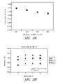
- FIG. 2Ashows the growth rate of silicon dioxide from hexakis(ethylamino) disilane and ozone at various deposition temperatures.
- FIG. 2Bshows the repeatability of the deposition across various wafers.
- FIG. 3Ashows the linearity of growth of silicon dioxide from hexakis(ethylamino) disilane and ozone.
- FIG. 3Bshows the growth rate (squares) and non-uniformity (diamonds) at 100, 250 and 500 cycles.
- FIG. 4Ashows the concentration of C and N and the Si:O ratio in silicon dioxide films deposited from hexakis(ethylamino) disilane and ozone at various deposition temperatures.
- FIG. 4Bshows the XRR density of the films and
- FIG. 4Cis an SEM image of a silicon dioxide film deposited at 300° C.
- FIG. 5illustrates the change in growth rate (squares) and non-uniformity (diamonds) observed at various silicon precursor evaporation temperatures (° C.).
- FIG. 6illustrates the thickness variations between the wafers (i.e. wafer to wafer uniformities) of approximately 400 ⁇ films from a batch load of 120 wafers.
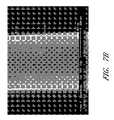
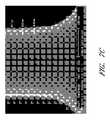
- FIGS. 7A-7Dillustrate step coverage of about 100%+/ ⁇ 5% of about 400 ⁇ thick SiO 2 films.
- FIGS. 7A-7Care enlarged portions of FIG. 7D .
- ALD type processesare based on controlled, self-limiting surface reactions of precursor chemicals. Gas phase reactions are avoided by feeding the precursors alternately and sequentially into the reaction chamber. Vapor phase reactants are separated from each other in the reaction chamber. Excess reactants and/or reactant byproducts are typically removed from the reaction chamber between reactant pulses.
- ALD processesare preferred to chemical vapor deposition processes (CVD) in some applications because the self limiting nature of ALD processes provides advantages such as greater control of film growth and better surface coverage.
- Silicon dioxide thin films and films comprising silicon dioxideare grown in an ALD reactor, preferably at the temperature of about 20-500° C., more preferably about 150-350° C., still more preferably about 250-300° C.
- Even flat (such as glass or wafer) or grooved flat materialscan be used as a substrate.
- On the surface of the substratecan also exist a so-called HSG (hemispherical grain) structure on which the film is grown.
- a powdery materialwhich has a large surface area, can be used as a substrate.
- growth substratedesignates in this invention the surface on which the thin film is grown. The surface can consist of the above-mentioned substrate or of a thin film grown onto the substrate or of another structure.
- Silicon dioxidehas a wide variety of applications, as will be apparent to the skilled artisan. For example it may be used to fill trenches as in STI (shallow trench isolation), as discussed below, or in forming spacers. Although several examples are described herein, other applications will be apparent to the skilled artisan.
- Silicon dioxidecan be used in STI structures.
- the function of STIis to isolate the transistors from each other in both the circuit and memory structures.
- LOCOS isolationis in use, which isolation is not suitable in the future circuits because of its bulkiness.
- STI trenchescan be filled but often the trench has to be widened in the upper part in order to avoid void formation in the middle of the STI isolation.
- ALDis an especially suitable process for producing STI because ALD is characterized by the ability to grow silicon dioxide of uniform quality and without void formation on uneven growth substrates, especially also onto narrow trenches. Using ALD enables thus a narrower isolation area between the circuits whereby the packing density of the circuits can be increased.
- silicon dioxidecan be used as the isolation layer in both the writing/reading head and in the encapsulation of the writing/reading head.
- the processing temperaturemust be low in all steps.
- physical (sputtering) methodsare used in the field, the problem of said methods being the unevenness of produced film.
- ALDhas the capability to produce both physically and electrically homogenous thin films. It is especially preferable to use a relatively low temperature ALD silicon dioxide process that provides a uniformly covering and electrically homogenous SiO 2 thin film. In this way the reproducibility and reliability of this process step can be increased.
- Film deposition methods producing uniform thin film on a large surfaceare needed for field emission displays (FED). Due to the relatively low growth temperature and the uniformity of the silicon dioxide film produced, the ALD silicon dioxide processes disclosed herein are suitable for preparing the dielectric layer for field emission displays.
- an “ALD process”designates a process in which deposition of material onto a surface is based on sequential and alternating self-saturating surface reactions.
- ALDALD
- conditions for ALDinclude a temperature window wherein the substrate is above the temperature at which source gases condense and below the temperature at which the source gases thermally decompose.
- reaction spaceis used to designate a reactor or reaction chamber, or an arbitrarily defined volume therein, in which conditions can be adjusted to effect thin film growth by ALD.
- reaction spaceincludes surfaces subject to all reaction gas pulses from which gases or particles can flow to the substrate, by entrained flow or diffusion, during normal operation.
- Adsorptionis used to designate a chemical attachment of atoms or molecules on a surface.
- “Surface”is used to designate a boundary between the reaction space and a feature of a substrate.
- Thin filmmeans a film that is grown from elements or compounds that are transported as separate ions, atoms or molecules via vacuum, gaseous phase or liquid phase from the source to the substrate.
- the thickness of the filmdepends upon the application and may vary in a wide range, preferably from about one molecular layer to 1,000 nm.
- ALDatomic layer deposition
- a substrate or workpiece placed in a reaction chamberis subjected to alternately repeated surface reactions.
- thin filmsare formed by repetition of a self-limiting ALD cycle.
- each ALD cyclecomprises at least two distinct phases.
- One reactantwill form no more than about one monolayer on the substrate surface and includes silicon.
- This reactantalso referred to herein as “the silicon reactant,” is preferably a disilane compound and in some embodiments is hexakis(ethylamino)disilane.
- a second reactant comprising a reactive oxygen speciesconverts the adsorbed silicon compound to silicon dioxide.
- at least three different source chemicalsare alternatively employed, corresponding to three phases.
- the substrate on which deposition is desiredpreferably a semiconductor workpiece
- the reactormay be part of a cluster tool in which a variety of different processes in the formation of an integrated circuit are carried out.
- a flow-type reactoris utilized.
- a high-volume manufacturing capable single wafer ALD reactoris used.
- a batch reactorcomprising multiple substrates is used.
- the substrate sizemay be, for example, greater than or equal to 200 mm and preferably is in the range of about 200 mm to about 675 mm. More preferably the substrate size is 300 mm.
- the substrate sizecan be in the range of about 500 ⁇ 500 mm 2 to about 2000 ⁇ 2000 mm 2 or even more.
- the number of substratesis preferably in the range of 10 to 200, more preferably in the range of 50 to 150, and most preferably in the range of 100 to 130.
- Exemplary single wafer reactorsdesigned specifically to enhance ALD processes, are commercially available from ASM America, Inc. (Phoenix, Ariz.) under the tradenames Pulsar® 2000 and Pulsar® 3000.
- Exemplary batch ALD reactorsdesigned specifically to enhance ALD processes, are commercially available from and ASM Europe B.V (Almere, Netherlands) under the tradenames A4ALDTM and A412TM.
- the exposed surfaces of the workpiececan be terminated to react with the first phase of the ALD process. In some embodiments a separate termination step is not required.
- a first reactant pulseis supplied to the workpiece.
- the first reactant pulsecomprises a carrier gas flow and a volatile silicon species, preferably an amino disilane compound, that is reactive with the workpiece surfaces of interest. Accordingly, the disilane compound adsorbs upon the workpiece surfaces.
- the first reactant pulseself-saturates the workpiece surfaces such that any excess constituents of the first reactant pulse do not further react with the molecular layer formed by this process.
- the first silicon reactant pulseis preferably supplied in gaseous form.
- the silicon reactant gasis considered “volatile” for purposes of the present description if the species exhibits sufficient vapor pressure under the process conditions to transport the species to the workpiece in sufficient concentration to saturate exposed surfaces.
- the first reactantis then removed from the reaction space.
- the flow of the first chemistryis stopped while continuing to flow a carrier gas for a sufficient time to diffuse or purge excess reactants and reactant by-products, if any, from the reaction space, preferably with greater than about two reaction chamber volumes of the purge gas, more preferably with greater than about three chamber volumes.
- pulse and purge times usedcan vary depending on the type of reactor. For example, pulse/purge times are usually shorter in embodiments with single wafer reactors. Pulse/purge times are usually longer in embodiments with batch reactors because multiple substrates are processed.
- the silicon reactant pulsing timeis from about 0.05 to about 180 seconds. However, depending on the reactor type, substrate type and its surface area, the pulsing time may be even higher than 180 seconds. In some embodiments, pulsing times can be on the order of minutes. The optimum pulsing time can be readily determined by the skilled artisan based on the particular circumstances.
- the silicon reactant in single wafer reactorsis provided with a pulse length of from about 0.1 to about 5 seconds, more preferably about 0.3 to about 1.5 seconds.
- the silicon reactant in batch ALD reactorsis provided with a pulse length of from about 1 to about 180 seconds, more preferably about 10 to about 60 seconds.
- the removal of excess reactantcomprises continuing to flow purge gas for between about 0.1 seconds and 20 seconds after stopping the flow of the first silicon reactant pulse.
- the adsorption and reactant removalrepresent a first phase in an ALD cycle, and can be referred to as the silicon phase. Longer purge times than 20 seconds may be used in some embodiments, for example for batch ALD processes.
- a second reactant pulseis then supplied to the workpiece.
- the second chemistrycomprises an oxygen source which desirably reacts with or adsorbs upon the molecular layer left by the first reactant to form silicon dioxide.
- the second reactant pulsecomprises supplying ozone to the workpiece, for example with the aid of a carrier gas.
- ozoneis provided as a mixture of ozone and oxygen (or an inert gas), comprising an ozone concentration of about 5 vol-% to about 40 vol-%.
- other oxygen sourcessuch as atomic oxygen, oxygen plasma or oxygen radicals, can be used.
- the oxygen source pulsing timeis from about 0.05 to about 180 seconds. However, depending on the reactor type, substrate type and its surface area, the pulsing time may be even higher than 180 seconds. In some embodiments, pulsing times can be on the order of minutes. The optimum pulsing time can be readily determined by the skilled artisan based on the particular circumstances.
- the pulse length of the oxygen source compound in a single wafer reactoris preferably from about 0.1 to about 5 seconds, more preferably from about 0.3 to about 1.5 seconds.
- the pulse length of the oxygen source compound in a batch ALD reactoris preferably from about 1 to about 60 seconds, more preferably from about 5 to about 30 seconds.
- any excess second reactantis removed from the reaction space.
- this stepmay comprise stopping the flow of the second reactant and continuing to flow carrier gas for a time period sufficient for excess reactants and volatile reaction by-products from the second reactant pulse to diffuse out of and be purged from the reaction space.
- the removal of excess reactantcomprises continuing to flow purge gas for between about 0.1 seconds and 20 seconds after stopping the flow of the second reactant pulse.
- the first reactant phasegenerally reacts with the termination left by the second phase in the previous cycle. Thus, while no reactant may be previously adsorbed on the substrate surface or present in the reaction space if the oxidation phase is the first phase in the first ALD cycle, in subsequent cycles the oxidation phase will effectively follow the silicon phase.
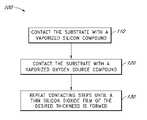
- FIG. 1is a flow chart generally illustrating a method for forming a silicon dioxide thin film in accordance with one embodiment.
- a silicon dioxide thin filmis formed on a substrate by an ALD type process 100 comprising multiple silicon dioxide deposition cycles, each silicon dioxide deposition cycle comprising:
- the silicon dioxide deposition cycleThis can be referred to as the silicon dioxide deposition cycle.
- the substrateis contacted with a vaporized silicon compound 110 .
- a vaporized silicon compound 110Any of the silicon precursors described herein can be used.
- the adsorbed silicon compoundcan be converted to silicon dioxide by contacting the substrate with a vaporized oxygen source compound 120 .
- Any of the oxygen precursors described hereincan be used as the oxygen source compound.
- the contacting stepsare repeated 130 until a thin film of a desired thickness and composition is obtained.
- additional chemistriescan also be included in each cycle or in various cycles throughout the deposition process.
- the cyclecan be extended to include a distinct surface preparation.
- one or more additional phasescan be conducted in each cycle.
- additional phasesmay be included that add additional components to the growing thin film, such as additional oxides to form a multicomponent oxide film.
- the depositioncan be carried out at a wide range of pressure conditions, but it is preferred to operate the process at reduced pressure.
- the pressure in the reaction chamberis typically from about 0.01 to about 500 mbar or more. However, in some cases the pressure will be higher or lower than this range, as can be readily determined by the skilled artisan.
- the pressure in a single wafer reactoris preferably maintained between about 0.01 mbar and 50 mbar, more preferably between about 0.1 mbar and 10 mbar.
- the pressure in a batch ALD reactoris preferably maintained between about 1 mTorr and 500 mTorr, more preferably between about 30 mTorr and 200 mTorr.
- the deposition temperatureis kept low enough to prevent thermal decomposition of the gaseous source chemicals.
- the deposition temperatureis kept high enough to provide activation energy for the surface reactions, to prevent the physisorption of source materials and minimize condensation of gaseous reactants in the reaction space.
- the deposition temperatureis typically about 20° C. to about 500° C., preferably about 150° C. to about 350° C., more preferably about 250° C. to about 300° C.
- the silicon source temperatureis preferably set below the deposition or substrate temperature. This is based on the fact that if the partial pressure of the source chemical vapor exceeds the condensation limit at the substrate temperature, controlled layer-by-layer growth of the thin film is compromised.
- the silicon source temperatureis from about 30 to about 150° C. In some embodiments the silicon source temperature is greater than about 60° C. during the deposition. In some embodiments, where greater doses are needed, for example in batch ALD, the silicon source temperature is from about 90° C. to about 200° C., preferably from about 130° C. to about 170° C.
- the growth rate of the thin film comprising silicon dioxideis preferably above 0.7 ⁇ /cycle. In other embodiments the growth rate is above 0.8 ⁇ /cycle and in still other embodiments the growth rate is above 1.0 ⁇ /cycle, and preferably in the range of 1.0 to 1.2 ⁇ /cycle.
- the deposited thin films comprising silicon dioxidehas less than 2 at-% of nitrogen as an impurity. In other embodiments the films comprise less than 1 at-% of nitrogen, or even less than 0.5 at-% nitrogen as an impurity. Similarly, in some embodiments the thin films comprise less than 1 at-% carbon as an impurity and in some cases less than 0.5 at-% carbon as an impurity.
- the deposited films comprising silicon oxidehas a step coverage of more than 80%, in other embodiments preferably more than 90% and in other embodiments preferably more than 95%.
- the source materialsare preferably selected to provide sufficient vapor pressure, sufficient thermal stability at substrate temperature, and sufficient reactivity of the compounds for effecting deposition by ALD.
- “Sufficient vapor pressure”typically supplies enough source chemical molecules in the gas phase to the substrate surface to enable self-saturated reactions at the surface at the desired rate.
- “Sufficient thermal stability”typically means that the source chemical itself does not form growth-disturbing condensable phases on the surface or leave harmful level of impurities on the substrate surface through thermal decomposition. In other words, temperatures are kept above the condensation limits and below the thermal decomposition limits of the selected reactant vapors.
- One aimis to avoid uncontrolled condensation of molecules on the substrate.
- “Sufficient reactivity”typically results in self-saturation in pulses short enough to allow for a commercially acceptable throughput time. Further selection criteria include the availability of the chemical at high purity and the ease of handling of the chemical.
- the silicon compoundis preferably a disilane and has a Si—Si bond.
- Organic compounds having a Si—Si bond and an NH x group either attached directly to silicon (to one or more silicon atoms) or to a carbon chain attached to siliconare used in some embodiments.
- organosilicon compoundsare used, which may or may not comprise Si—Si bonds. More preferably the silicon compound has the formula:
- xis selected from 1 to 3;
- yis selected from 1 to 3;
- R Iis selected from the group consisting of hydrogen, alkyl, and substituted alkyl
- R IIis selected from the group consisting of alkyl and substituted alkyl
- R IIIis selected from the group consisting of hydrogen, hydroxide (—OH), amino (—NH 2 ), alkoxy, alkyl, and substituted alkyl;
- each x, y, R III , R II and R Ican be selected independently from each other.
- the silicon compoundis hexakis(monoalkylamino)disilane:
- the silicon compoundis hexakis(ethylamino)disilane:
- the silicon compoundis (CH 3 —O) 3 —Si—Si—(O—CH 3 ) 3 (IV)
- the preferred silicon precursorsmay produce unexpectedly good deposition rates and uniformity because there is a Si—Si bond or because there is a catalytic NH group attached to the Si, or both of these factors.
- the silicon compoundcan be formed during the ALD process such that while the silicon compound is bonding, a new gas-phase silicon compound is formed which in turn is able to bond to hydroxyl and, optionally oxide groups of the growth substrate. This phenomenon is called “in situ” formation of silicon compound.
- a suitable reactive oxygen sourceis introduced into the reaction space to convert the silicon compound to silicon dioxide.
- Preferred oxygen source materialsare for example water, oxygen, atomic oxygen, oxygen plasma, oxygen radicals, hydrogen peroxide and the aqueous solutions of hydrogen peroxide and ozone.
- oxygen sourcesare used which are more reactive than water towards silicon compounds which contain an organic ligand.
- the oxygen source materialis ozone (O 3 ).
- Ozonecan be produced by an ozone generator and it is most preferably introduced into the reaction space with the aid of an inert gas of same kind, such as nitrogen, or with the aid of oxygen.
- ozoneis provided at a concentration of from about 5 vol-% to about 40 vol-%, and preferably from about 15 vol-% to about 25 vol-%.
- One or more of the following compoundscan also be used as the oxygen source material:
- methods for forming a silicon dioxide thin film on a substrate in a reaction chamber by atomic layer depositioncomprise a deposition cycle comprising: providing a vapor phase pulse of a first reactant comprising a first silicon source precursor to the reaction chamber such that it forms no more than a monolayer on the substrate; removing excess first reactant from the reaction chamber; providing a vapor phase pulse of a second reactant comprising an oxygen source to the reaction chamber; and removing excess second reactant and any reaction byproducts from the reaction chamber; wherein the providing and removing steps are repeated until a thin silicon dioxide film of a desired thickness is obtained.
- the silicon compoundis hexakis(monoalkylamino)disilane (R II —NH) 3 —Si—Si—(NH—R II ) 3 and R II is selected from the group consisting of alkyl and substituted alkyl.
- R IIis hexakis(monoalkylamino)disilane (R II —NH) 3 —Si—Si—(NH—R II ) 3 and R II is selected from the group consisting of alkyl and substituted alkyl.
- the process conditionscan be as described herein.
- methods for forming a silicon dioxide thin film by atomic layer deposition on a substrate in a reaction chambercomprising: alternately and sequentially providing a vapor phase reactant pulse comprising a silicon precursor and a vapor phase reactant pulse comprising an oxygen precursor to the reaction chamber; wherein the vapor phase reactant pulses are repeated until a thin film of a desired thickness is obtained; wherein the silicon compound is hexakis(ethylamino)disilane (Et-NH) 3 —Si—Si—(NH-Et) 3 .
- the process conditionscan be as described herein.
- a multicomponent filmcan be achieved by changing the source material, i.e. by growing some other oxide onto the growth substrate between silicon dioxide growth cycles. From the point of view of the invention the growth order of the oxide compounds can be optional.
- a multicomponent oxidemay be grown by vaporising the metal source material and leading the vaporised metal source material onto the substrate on which it reacts forming one molecular layer on the surface via a ligand exchange reaction and/or dissociation reaction.
- the reaction spaceis purged carefully with an inert gas to remove the unreacted source material and the reaction products from the reaction space.
- the oxygen source materialcan be led into the reaction space, with the oxygen source material reacting with the remaining ligands of a chemisorbed metal compound complex (e.g. zirconium complex) forming new OH groups and oxygen bridges on the surface.
- the reaction spaceis purged again carefully.
- the above-described growing cycle of silicon dioxidecan be carried out.
- One or wore metals or semimetalscan function as the second cation of the multicomponent oxide (i.e. tertiary oxide).
- Metals belonging to the groups IIIa, IVa and Va (transition metals) of the periodic table of the elements including the rare earth metals, i.e., lanthane and lanthanoids, as well as the metals and semimetals of group IVbcan especially be mentioned of the metals.
- any stable vaporisable compound of metal in questioncan be used.
- the following metal source materialscould be used: aluminium chloride as an aluminium source material, titanium tetrachloride (TiCl 4 ), as a titanium source material, tantalum pentachloride (TaCl 5 ) as a tantalum source material, hafnium tetrachloride (HfCl 4 ) as a hafnium source material, zirconium tetrachloride (ZrCl 4 ) as a zirconium source material, yttrium betadiketonate (Y(thd) 3 ) as a yttrium source material and lanthanum betadiketonate (La(thd) 3 ) as a lanthanum source material.
- Other metal source materials that can be usedwill be apparent to the skilled artisan.
- Multicomponent films containing various concentrations of silicon dioxidee.g. SiAlO x , SiTiO x , SiTaO x , SiHfO x , SiZrO x , SiYO x , SiLaO x can be grown according to the invention by changing the number of reaction cycles of the silicon source material and ozone (or other oxygen source) as compared to reaction cycles of another metal source material.
- the amount of oxidecan vary and the oxide is not always completely stoichiometric.
- the ratio of the amount of the metal oxide and silicon dioxide cyclescan be varied to achieve the desired composition.
- the metal oxide cycle/silicon dioxide cycle ratioin question e.g. from 10:1 to 1:10 the nature of the mixed oxide can be varied in a controlled way from a complete mixed oxide to a nanolaminate structure.
- SiO 2 filmswere deposited in an atomic layer deposition process using hexakis(ethylamino) disilane and O 3 .
- Hexakis(ethylamino) disilaneis a liquid Si precursor with relatively low vapour pressure.
- a vaporization temperature of 110° C.was used.
- the depositionwas carried out on 200 mm silicon wafers in an ASM Pulsar®2000 ALCVDTM reactor. Deposition temperature was varied from 150 to 300° C.
- Film thickness and uniformitywere measured using a spectroscopic ellipsometer.
- X-ray reflectometryXRR was also used for confirming the thickness as well as for determining the film density.
- the film compositionwas studied by both Rutherford backscattering spectroscopy (RBS) and X-ray photoelectron spectroscopy (XPS).
- FIG. 2AGrowth rates ( ⁇ /cycle) at the various temperatures are presented in FIG. 2A .
- the repeatability of the process at 250° C.is illustrated in FIG. 2B .
- FIG. 3Ashows the linearity of growth observed at 200° C.
- FIG. 3Billustrates the growth rate (squares) and non-uniformity (diamonds) is relatively constant from 100 to 500 cycles.
- FIG. 4Aprovides concentrations of carbon and nitrogen impurities at various temperatures, as well as the resultant Si:O ratio.
- FIG. 4Bprovides the XRR density at the various temperatures and
- FIG. 4Cshows an SEM of a silicon oxide film.
- FIG. 5shows an increase in growth rate (squares) and a decrease in non-uniformity (diamonds) over the initial cycles in the deposition process at various silicon precursor temperatures (° C.).
- the film thickness and uniformityappeared to depend on deposition temperature and precursor dose.
- the O 3 doseaffected the uniformity and growth rate.
- the highest growth rateswere above 1 ⁇ /cycle and were obtained at the lower temperatures of 150-200° C.
- the best film uniformitieswere obtained at the highest temperature of 300° C.
- the refractive indexwas the same 1.44 for all the films regardless of deposition temperature.
- the composition of the filmmatches SiO 2 according to XPS. Also RBS gave the same Si:O ratio of 0.5.
- the filmscontain hydrogen, and also some nitrogen and carbon as impurities.
- SiO 2 filmswere deposited in a batch atomic layer deposition process using hexakis(ethylamino)disilane and O 3 .
- the depositionwas carried out on 300 mm silicon wafers in an ASM A412TM reactor using two injectors, one for each precursor, and with a load of 120 wafers.
- the deposition temperaturewas fixed at about 300° C.
- the hexakis(ethylamino)disilane precursor evaporation ratewas about 20 g/hr, which resulted in a flow rate of about 23 sccm from the evaporator.
- the evaporatorwas at a temperature of 148° C.
- the disilane precursor pulseswere about 30 s.
- the oxygen sourcewas ozone, with an ozone flow rate of about 3000 sccm.
- the ozone pulseswere about 10 s.
- a purging and evacuation step of 10 swas used between the pulses.
- a scanning electron microscope (SEM)was used to determine the step coverage.
- the growth ratewas about 1.1 ⁇ /cycle. Within wafer uniformities (thickness variation across a single wafer) of less than 0.5% (full range) were achieved. Minimal thickness variations of less than about 0.2% between the wafers (i.e. wafer to wafer uniformities) of approximately 400 ⁇ films from a batch load of 120 wafers are presented in FIG. 6 . A step coverage of about 100%+/ ⁇ 5% of the films is illustrated in the SEM images in FIGS. 7A-7D .
Landscapes
- Chemical & Material Sciences (AREA)
- Engineering & Computer Science (AREA)
- Chemical Kinetics & Catalysis (AREA)
- General Chemical & Material Sciences (AREA)
- Materials Engineering (AREA)
- Mechanical Engineering (AREA)
- Metallurgy (AREA)
- Organic Chemistry (AREA)
- Inorganic Chemistry (AREA)
- Physics & Mathematics (AREA)
- General Physics & Mathematics (AREA)
- Manufacturing & Machinery (AREA)
- Computer Hardware Design (AREA)
- Microelectronics & Electronic Packaging (AREA)
- Power Engineering (AREA)
- Condensed Matter Physics & Semiconductors (AREA)
- Chemical Vapour Deposition (AREA)
- Formation Of Insulating Films (AREA)
Abstract
Description
- The present application claims priority under 35 U.S.C. § 119(e) to U.S. Provisional Application No. 61/015,966 filed Dec. 21, 2007, entitled SILICON DIOXIDE THIN FILMS BY ALD, which is hereby incorporated by reference in its entirety.
- 1. Field of the Invention
- The present disclosure provides methods for depositing oxide thin films by atomic layer deposition (ALD). More particularly thin films comprising silicon dioxide are deposited using disilane compounds.
- 2. Description of the Related Art
- Silicon dioxide is a widely used material in semiconductor industry. It is used for instance as gate oxide and a dielectric layer in dynamic random access memories (DRAM). Recently, other possible applications have evolved that would require good step coverage and good SiO2filling capabilities, for example shallow trench isolation (STI). Atomic layer deposition (ALD) has been proposed as a possible technique to meet these more stringent requirements. Unfortunately, the growth rate per cycle has traditionally been low for ALD SiO2processes making the processing economically non-viable. New precursors with higher reactivity enabling higher growth rate are therefore needed.
- In its various forms Chemical Vapor Deposition (CVD) is the most frequently used method of producing silicon dioxide (see patent publications JP 9306906, U.S. Pat. No. 4,845,054, U.S. Pat. No. 4,981,724, U.S. Pat. No. 5,462,899, JP 20868486, JP 6158329, JP 80061810, U.S. Pat. No. 4,872,947, JP 7026383, U.S. Pat. No. 5,855,957 and U.S. Pat. No. 5,849,644). Mainly tetraethoxy silane (TEOS) has been used as the silicon source material, and oxygen, water, hydrogen peroxide or ozone have been used as the oxygen source material in the patent publications. In the conventional CVD the oxygen source material is always brought simultaneously with the silicon source material to the growth substrate.
- Conventional CVD methods provide neither sufficiently good coverage nor the level of conformality desired for some applications.
- Atomic layer deposition (ALD), originally known as atomic layer epitaxy (ALE), is an advanced form of vapor deposition. ALD processes are based on sequential, self-saturated surface reactions. Examples of these processes are described in detail in U.S. Pat. Nos. 4,058,430 and 5,711,811. Due to the self-saturating nature of the process, ALD enables almost perfectly conformal deposition of films on an atomic level and precise control of the thickness and composition of the deposited films.
- Silicon dioxide has been gown by ALD processes using compounds such as Si(NCO)4and N(C2H5)3(K. Yamaguchi et al., Appl. Surf. Sci. (1998) 130-132) as source materials. Deposition of silicon dioxide by Molecular Layer ALE and UHV-ALE processes using SiCl4and H2O as source materials is also described in the literature (Surface Review and Letters, Vol. 6,
Nos 3 & 4 (1999) 435-448). However, these processes have long reaction times and cannot be realized on an industrial scale. - According to one aspect of the invention, methods for depositing a thin film comprising silicon oxide on a substrate by atomic layer deposition are provided. The methods generally comprise contacting a substrate in a reaction space with a first reactant that includes a silicon source chemical, preferably a disilane compound as described herein, and a second reactant comprising an oxygen source, thereby forming the silicon oxide thin film on the substrate.
- According to some embodiments of the invention, atomic layer deposition (ALD) processes for growing a thin film over a substrate are provided. The methods generally comprise alternately and sequentially contacting a substrate in a reaction space with vapor phase pulses of an amino disilane compound, such as hexakis(ethylamino)disilane, that forms no more than about one molecular layer on the structural surface of the substrate, and a second reactant comprising a reactive oxygen source, such as ozone.
- For purposes of summarizing the invention and the advantages achieved over the prior art, certain objects and advantages of the invention have been described herein. Of course, it is to be understood that not necessarily all such objects or advantages may be achieved in accordance with any particular embodiment of the invention. Thus, for example, those skilled in the art will recognize that the invention may be embodied or carried out in a manner that achieves or optimizes one advantage or group of advantages as taught herein without necessarily achieving other objects or advantages as may be taught or suggested herein.
- All of the embodiments described herein are intended to be within the scope of the invention herein disclosed. These and other embodiments of the present invention will be readily apparent to those skilled in the art from the following detailed description of the preferred embodiments having reference to the attached figures, the invention not being limited to any particular preferred embodiment(s) disclosed.
- These and other aspects of the invention will be readily apparent to the skilled artisan in view of the description below and the appended drawings, which are meant to illustrate and not to limit the invention, and in which:
FIG. 1 is a block diagram of a pulsing sequence in an ALD-type process according to some embodiments of the invention.FIG. 2A shows the growth rate of silicon dioxide from hexakis(ethylamino) disilane and ozone at various deposition temperatures.FIG. 2B shows the repeatability of the deposition across various wafers.FIG. 3A shows the linearity of growth of silicon dioxide from hexakis(ethylamino) disilane and ozone.FIG. 3B shows the growth rate (squares) and non-uniformity (diamonds) at 100, 250 and 500 cycles.FIG. 4A shows the concentration of C and N and the Si:O ratio in silicon dioxide films deposited from hexakis(ethylamino) disilane and ozone at various deposition temperatures.FIG. 4B shows the XRR density of the films andFIG. 4C is an SEM image of a silicon dioxide film deposited at 300° C.FIG. 5 illustrates the change in growth rate (squares) and non-uniformity (diamonds) observed at various silicon precursor evaporation temperatures (° C.).FIG. 6 illustrates the thickness variations between the wafers (i.e. wafer to wafer uniformities) of approximately 400 Å films from a batch load of 120 wafers.FIGS. 7A-7D illustrate step coverage of about 100%+/−5% of about 400 Å thick SiO2films.FIGS. 7A-7C are enlarged portions ofFIG. 7D .- ALD type processes are based on controlled, self-limiting surface reactions of precursor chemicals. Gas phase reactions are avoided by feeding the precursors alternately and sequentially into the reaction chamber. Vapor phase reactants are separated from each other in the reaction chamber. Excess reactants and/or reactant byproducts are typically removed from the reaction chamber between reactant pulses.
- ALD processes are preferred to chemical vapor deposition processes (CVD) in some applications because the self limiting nature of ALD processes provides advantages such as greater control of film growth and better surface coverage.
- Silicon dioxide thin films and films comprising silicon dioxide are grown in an ALD reactor, preferably at the temperature of about 20-500° C., more preferably about 150-350° C., still more preferably about 250-300° C. Even flat (such as glass or wafer) or grooved flat materials can be used as a substrate. On the surface of the substrate can also exist a so-called HSG (hemispherical grain) structure on which the film is grown. Additionally, a powdery material, which has a large surface area, can be used as a substrate. The term “growth substrate” designates in this invention the surface on which the thin film is grown. The surface can consist of the above-mentioned substrate or of a thin film grown onto the substrate or of another structure.
- Silicon dioxide has a wide variety of applications, as will be apparent to the skilled artisan. For example it may be used to fill trenches as in STI (shallow trench isolation), as discussed below, or in forming spacers. Although several examples are described herein, other applications will be apparent to the skilled artisan.
- Silicon dioxide can be used in STI structures. The function of STI is to isolate the transistors from each other in both the circuit and memory structures. At present in the lateral direction wide so-called LOCOS isolation is in use, which isolation is not suitable in the future circuits because of its bulkiness. In STI technology a horizontal narrow deep trench filled with dielectric=silicon dioxide, is etched between the circuits. Since the depth of the trench is greater than the width STI requires a method which is capable of filling the etched isolation trench conformally. By the conventional CVD method STI trenches can be filled but often the trench has to be widened in the upper part in order to avoid void formation in the middle of the STI isolation. Enlargement of the trench leads to increase of the STI area, i.e., the area of the isolation area increases. ALD is an especially suitable process for producing STI because ALD is characterized by the ability to grow silicon dioxide of uniform quality and without void formation on uneven growth substrates, especially also onto narrow trenches. Using ALD enables thus a narrower isolation area between the circuits whereby the packing density of the circuits can be increased.
- In the components needed in magnetic recording, silicon dioxide can be used as the isolation layer in both the writing/reading head and in the encapsulation of the writing/reading head. In order to avoid the destruction of the magnetic properties of the layers, that are already built, the processing temperature must be low in all steps. In general, physical (sputtering) methods are used in the field, the problem of said methods being the unevenness of produced film. ALD has the capability to produce both physically and electrically homogenous thin films. It is especially preferable to use a relatively low temperature ALD silicon dioxide process that provides a uniformly covering and electrically homogenous SiO2thin film. In this way the reproducibility and reliability of this process step can be increased.
- Film deposition methods producing uniform thin film on a large surface are needed for field emission displays (FED). Due to the relatively low growth temperature and the uniformity of the silicon dioxide film produced, the ALD silicon dioxide processes disclosed herein are suitable for preparing the dielectric layer for field emission displays.
- For the purpose of the present description, an “ALD process” designates a process in which deposition of material onto a surface is based on sequential and alternating self-saturating surface reactions. The general principles of ALD are disclosed, e.g., in U.S. Pat. Nos. 4,058,430 and 5,711,811, the disclosures of which are incorporated herein by reference. Generally, conditions for ALD include a temperature window wherein the substrate is above the temperature at which source gases condense and below the temperature at which the source gases thermally decompose.
- “Reaction space” is used to designate a reactor or reaction chamber, or an arbitrarily defined volume therein, in which conditions can be adjusted to effect thin film growth by ALD. Typically the reaction space includes surfaces subject to all reaction gas pulses from which gases or particles can flow to the substrate, by entrained flow or diffusion, during normal operation.
- “Adsorption” is used to designate a chemical attachment of atoms or molecules on a surface.
- “Surface” is used to designate a boundary between the reaction space and a feature of a substrate.
- “Thin film” means a film that is grown from elements or compounds that are transported as separate ions, atoms or molecules via vacuum, gaseous phase or liquid phase from the source to the substrate. The thickness of the film depends upon the application and may vary in a wide range, preferably from about one molecular layer to 1,000 nm.
- The methods presented herein allow deposition of silicon dioxide films on substrate surfaces. Geometrically challenging applications are also possible due to the self-limited nature of the surface reactions. According to the preferred embodiments, atomic layer deposition (ALD) type processes are used to form silicon dioxide films on substrates, such as integrated circuit workpieces.
- A substrate or workpiece placed in a reaction chamber is subjected to alternately repeated surface reactions. In particular, thin films are formed by repetition of a self-limiting ALD cycle. Preferably, each ALD cycle comprises at least two distinct phases. One reactant will form no more than about one monolayer on the substrate surface and includes silicon. This reactant, also referred to herein as “the silicon reactant,” is preferably a disilane compound and in some embodiments is hexakis(ethylamino)disilane. A second reactant comprising a reactive oxygen species converts the adsorbed silicon compound to silicon dioxide. In the case of multicomponent oxide thin film deposition, at least three different source chemicals are alternatively employed, corresponding to three phases.
- In preferred embodiments the substrate on which deposition is desired, preferably a semiconductor workpiece, is loaded into a reactor. The reactor may be part of a cluster tool in which a variety of different processes in the formation of an integrated circuit are carried out. In some embodiments a flow-type reactor is utilized. In some embodiments a high-volume manufacturing capable single wafer ALD reactor is used. In other embodiments a batch reactor comprising multiple substrates is used. The substrate size may be, for example, greater than or equal to 200 mm and preferably is in the range of about 200 mm to about 675 mm. More preferably the substrate size is 300 mm. However, in some cases, such as for applications outside of integrated circuits like solar cells and display technology, the substrate size can be in the range of about 500×500 mm2to about 2000×2000 mm2or even more. For embodiments in batch ALD reactors, the number of substrates is preferably in the range of 10 to 200, more preferably in the range of 50 to 150, and most preferably in the range of 100 to 130.
- Exemplary single wafer reactors, designed specifically to enhance ALD processes, are commercially available from ASM America, Inc. (Phoenix, Ariz.) under the tradenames Pulsar® 2000 and Pulsar® 3000. Exemplary batch ALD reactors, designed specifically to enhance ALD processes, are commercially available from and ASM Europe B.V (Almere, Netherlands) under the tradenames A4ALD™ and A412™.
- In some embodiments, if necessary, the exposed surfaces of the workpiece can be terminated to react with the first phase of the ALD process. In some embodiments a separate termination step is not required.
- After the initial surface termination, if necessary, a first reactant pulse is supplied to the workpiece. In accordance with some embodiments, the first reactant pulse comprises a carrier gas flow and a volatile silicon species, preferably an amino disilane compound, that is reactive with the workpiece surfaces of interest. Accordingly, the disilane compound adsorbs upon the workpiece surfaces. The first reactant pulse self-saturates the workpiece surfaces such that any excess constituents of the first reactant pulse do not further react with the molecular layer formed by this process.
- The first silicon reactant pulse is preferably supplied in gaseous form. The silicon reactant gas is considered “volatile” for purposes of the present description if the species exhibits sufficient vapor pressure under the process conditions to transport the species to the workpiece in sufficient concentration to saturate exposed surfaces.
- After sufficient time for a molecular layer to adsorb on the substrate surface, the first reactant is then removed from the reaction space. In some embodiments the flow of the first chemistry is stopped while continuing to flow a carrier gas for a sufficient time to diffuse or purge excess reactants and reactant by-products, if any, from the reaction space, preferably with greater than about two reaction chamber volumes of the purge gas, more preferably with greater than about three chamber volumes.
- The pulse and purge times used can vary depending on the type of reactor. For example, pulse/purge times are usually shorter in embodiments with single wafer reactors. Pulse/purge times are usually longer in embodiments with batch reactors because multiple substrates are processed.
- Typically, the silicon reactant pulsing time is from about 0.05 to about 180 seconds. However, depending on the reactor type, substrate type and its surface area, the pulsing time may be even higher than 180 seconds. In some embodiments, pulsing times can be on the order of minutes. The optimum pulsing time can be readily determined by the skilled artisan based on the particular circumstances.
- In some embodiments, the silicon reactant in single wafer reactors is provided with a pulse length of from about 0.1 to about 5 seconds, more preferably about 0.3 to about 1.5 seconds.
- In some embodiments, the silicon reactant in batch ALD reactors is provided with a pulse length of from about 1 to about 180 seconds, more preferably about 10 to about 60 seconds.
- In some embodiments the removal of excess reactant comprises continuing to flow purge gas for between about 0.1 seconds and 20 seconds after stopping the flow of the first silicon reactant pulse. Together, the adsorption and reactant removal represent a first phase in an ALD cycle, and can be referred to as the silicon phase. Longer purge times than 20 seconds may be used in some embodiments, for example for batch ALD processes.
- In the second phase, a second reactant pulse is then supplied to the workpiece. The second chemistry comprises an oxygen source which desirably reacts with or adsorbs upon the molecular layer left by the first reactant to form silicon dioxide. In some embodiments the second reactant pulse comprises supplying ozone to the workpiece, for example with the aid of a carrier gas. In some embodiments ozone is provided as a mixture of ozone and oxygen (or an inert gas), comprising an ozone concentration of about 5 vol-% to about 40 vol-%. As discussed below, other oxygen sources, such as atomic oxygen, oxygen plasma or oxygen radicals, can be used.
- Typically, the oxygen source pulsing time is from about 0.05 to about 180 seconds. However, depending on the reactor type, substrate type and its surface area, the pulsing time may be even higher than 180 seconds. In some embodiments, pulsing times can be on the order of minutes. The optimum pulsing time can be readily determined by the skilled artisan based on the particular circumstances.
- The pulse length of the oxygen source compound in a single wafer reactor is preferably from about 0.1 to about 5 seconds, more preferably from about 0.3 to about 1.5 seconds. The pulse length of the oxygen source compound in a batch ALD reactor is preferably from about 1 to about 60 seconds, more preferably from about 5 to about 30 seconds.
- After a time period sufficient to completely saturate and react the molecular layer with the second reactant pulse, any excess second reactant is removed from the reaction space. As with the removal of the first reactant, this step may comprise stopping the flow of the second reactant and continuing to flow carrier gas for a time period sufficient for excess reactants and volatile reaction by-products from the second reactant pulse to diffuse out of and be purged from the reaction space. In some embodiments the removal of excess reactant comprises continuing to flow purge gas for between about 0.1 seconds and 20 seconds after stopping the flow of the second reactant pulse. Together, the second reactant pulse and removal represent a second phase in the illustrated process, and can also be considered the oxidation phase.
- The two phases together represent one ALD cycle, which is repeated to form silicon oxide thin films of the desired thickness. While the ALD cycle is generally referred to herein as beginning with the silicon phase, it is contemplated that in other embodiments the cycle may begin with the oxidation phase. One of skill in the art will recognize that the first reactant phase generally reacts with the termination left by the second phase in the previous cycle. Thus, while no reactant may be previously adsorbed on the substrate surface or present in the reaction space if the oxidation phase is the first phase in the first ALD cycle, in subsequent cycles the oxidation phase will effectively follow the silicon phase.
FIG. 1 is a flow chart generally illustrating a method for forming a silicon dioxide thin film in accordance with one embodiment. According to a preferred embodiment, a silicon dioxide thin film is formed on a substrate by anALD type process 100 comprising multiple silicon dioxide deposition cycles, each silicon dioxide deposition cycle comprising:- contacting a substrate with a vaporized silicon compound such that the silicon compound adsorbs to the substrate; and
- converting the adsorbed silicon compound into silicon dioxide by contacting it with a reactive vaporized oxygen source compound
- This can be referred to as the silicon dioxide deposition cycle. In the silicon
dioxide deposition cycle 100, the substrate is contacted with a vaporizedsilicon compound 110. Any of the silicon precursors described herein can be used. Next, the adsorbed silicon compound can be converted to silicon dioxide by contacting the substrate with a vaporizedoxygen source compound 120. Any of the oxygen precursors described herein can be used as the oxygen source compound. The contacting steps are repeated130 until a thin film of a desired thickness and composition is obtained. - Although described above in terms of two reactants, it will be understood that, in some embodiments, additional chemistries can also be included in each cycle or in various cycles throughout the deposition process. For example, if necessary, the cycle can be extended to include a distinct surface preparation. Moreover, one or more additional phases can be conducted in each cycle. For example, as discussed below, additional phases may be included that add additional components to the growing thin film, such as additional oxides to form a multicomponent oxide film.
- The deposition can be carried out at a wide range of pressure conditions, but it is preferred to operate the process at reduced pressure. The pressure in the reaction chamber is typically from about 0.01 to about 500 mbar or more. However, in some cases the pressure will be higher or lower than this range, as can be readily determined by the skilled artisan. The pressure in a single wafer reactor is preferably maintained between about 0.01 mbar and 50 mbar, more preferably between about 0.1 mbar and 10 mbar. The pressure in a batch ALD reactor is preferably maintained between about 1 mTorr and 500 mTorr, more preferably between about 30 mTorr and 200 mTorr.
- The deposition temperature is kept low enough to prevent thermal decomposition of the gaseous source chemicals. On the other hand, the deposition temperature is kept high enough to provide activation energy for the surface reactions, to prevent the physisorption of source materials and minimize condensation of gaseous reactants in the reaction space. Depending on the reactants and reactors, the deposition temperature is typically about 20° C. to about 500° C., preferably about 150° C. to about 350° C., more preferably about 250° C. to about 300° C.
- The silicon source temperature is preferably set below the deposition or substrate temperature. This is based on the fact that if the partial pressure of the source chemical vapor exceeds the condensation limit at the substrate temperature, controlled layer-by-layer growth of the thin film is compromised. In some embodiments, the silicon source temperature is from about 30 to about 150° C. In some embodiments the silicon source temperature is greater than about 60° C. during the deposition. In some embodiments, where greater doses are needed, for example in batch ALD, the silicon source temperature is from about 90° C. to about 200° C., preferably from about 130° C. to about 170° C.
- In some embodiments the growth rate of the thin film comprising silicon dioxide is preferably above 0.7 Å/cycle. In other embodiments the growth rate is above 0.8 Å/cycle and in still other embodiments the growth rate is above 1.0 Å/cycle, and preferably in the range of 1.0 to 1.2 Å/cycle.
- In some embodiments the deposited thin films comprising silicon dioxide has less than 2 at-% of nitrogen as an impurity. In other embodiments the films comprise less than 1 at-% of nitrogen, or even less than 0.5 at-% nitrogen as an impurity. Similarly, in some embodiments the thin films comprise less than 1 at-% carbon as an impurity and in some cases less than 0.5 at-% carbon as an impurity.
- In some embodiments the deposited films comprising silicon oxide has a step coverage of more than 80%, in other embodiments preferably more than 90% and in other embodiments preferably more than 95%.
- In general, the source materials, (e.g., silicon source materials), are preferably selected to provide sufficient vapor pressure, sufficient thermal stability at substrate temperature, and sufficient reactivity of the compounds for effecting deposition by ALD. “Sufficient vapor pressure” typically supplies enough source chemical molecules in the gas phase to the substrate surface to enable self-saturated reactions at the surface at the desired rate. “Sufficient thermal stability” typically means that the source chemical itself does not form growth-disturbing condensable phases on the surface or leave harmful level of impurities on the substrate surface through thermal decomposition. In other words, temperatures are kept above the condensation limits and below the thermal decomposition limits of the selected reactant vapors. One aim is to avoid uncontrolled condensation of molecules on the substrate. “Sufficient reactivity” typically results in self-saturation in pulses short enough to allow for a commercially acceptable throughput time. Further selection criteria include the availability of the chemical at high purity and the ease of handling of the chemical.
- In some embodiments, the silicon compound is preferably a disilane and has a Si—Si bond. Organic compounds having a Si—Si bond and an NHxgroup either attached directly to silicon (to one or more silicon atoms) or to a carbon chain attached to silicon are used in some embodiments. In some embodiments organosilicon compounds are used, which may or may not comprise Si—Si bonds. More preferably the silicon compound has the formula:
RIII3-x(RIIRIN)x—Si—Si—(N—RIRII)yRIII3-y, (I)- wherein the
- x is selected from 1 to 3;
- y is selected from 1 to 3;
- RIis selected from the group consisting of hydrogen, alkyl, and substituted alkyl;
- RIIis selected from the group consisting of alkyl and substituted alkyl; and
- RIIIis selected from the group consisting of hydrogen, hydroxide (—OH), amino (—NH2), alkoxy, alkyl, and substituted alkyl;
- and wherein the each x, y, RIII, RIIand RIcan be selected independently from each other.
- In some embodiments the silicon compound is hexakis(monoalkylamino)disilane:
(RII—NH)3—Si—Si—(NH—RII)3 (II)- In other embodiments the silicon compound is hexakis(ethylamino)disilane:
(Et-NH)3—Si—Si—(NH-Et)3 (II)- In other embodiments the silicon compound is (CH3—O)3—Si—Si—(O—CH3)3(IV)
- Without wishing to be held to a particular theory, the preferred silicon precursors may produce unexpectedly good deposition rates and uniformity because there is a Si—Si bond or because there is a catalytic NH group attached to the Si, or both of these factors.
- In some embodiments the silicon compound can be formed during the ALD process such that while the silicon compound is bonding, a new gas-phase silicon compound is formed which in turn is able to bond to hydroxyl and, optionally oxide groups of the growth substrate. This phenomenon is called “in situ” formation of silicon compound.
- As discussed above, after the silicon compound is removed, a suitable reactive oxygen source is introduced into the reaction space to convert the silicon compound to silicon dioxide. Preferred oxygen source materials are for example water, oxygen, atomic oxygen, oxygen plasma, oxygen radicals, hydrogen peroxide and the aqueous solutions of hydrogen peroxide and ozone. In some embodiments oxygen sources are used which are more reactive than water towards silicon compounds which contain an organic ligand. In the example provided below, the oxygen source material is ozone (O3). Ozone can be produced by an ozone generator and it is most preferably introduced into the reaction space with the aid of an inert gas of same kind, such as nitrogen, or with the aid of oxygen. In some embodiments ozone is provided at a concentration of from about 5 vol-% to about 40 vol-%, and preferably from about 15 vol-% to about 25 vol-%.
- One or more of the following compounds can also be used as the oxygen source material:
- oxides of nitrogen, such as N2O, NO and NO2,
- oxyhalide compounds, for example chlorodioxide (ClO2) and perchloroacid (HClO4),
- peracids (—O—O—H), for example perbenzoic acid (C6H5COOOH), and peracetic acid (CH3COOOH),
- alcohols, such as methanol (CH3OH) and ethanol (CH3CH2OH), and
- various radicals, for example oxygen radical (O) or hydroxyl radical (OH).
- In other preferred embodiments, methods for forming a silicon dioxide thin film on a substrate in a reaction chamber by atomic layer deposition are provided. The methods comprise a deposition cycle comprising: providing a vapor phase pulse of a first reactant comprising a first silicon source precursor to the reaction chamber such that it forms no more than a monolayer on the substrate; removing excess first reactant from the reaction chamber; providing a vapor phase pulse of a second reactant comprising an oxygen source to the reaction chamber; and removing excess second reactant and any reaction byproducts from the reaction chamber; wherein the providing and removing steps are repeated until a thin silicon dioxide film of a desired thickness is obtained. In some embodiments, the silicon compound is hexakis(monoalkylamino)disilane (RII—NH)3—Si—Si—(NH—RII)3and RIIis selected from the group consisting of alkyl and substituted alkyl. The process conditions can be as described herein.
- In other preferred embodiments, methods for forming a silicon dioxide thin film by atomic layer deposition on a substrate in a reaction chamber are provided comprising: alternately and sequentially providing a vapor phase reactant pulse comprising a silicon precursor and a vapor phase reactant pulse comprising an oxygen precursor to the reaction chamber; wherein the vapor phase reactant pulses are repeated until a thin film of a desired thickness is obtained; wherein the silicon compound is hexakis(ethylamino)disilane (Et-NH)3—Si—Si—(NH-Et)3. The process conditions can be as described herein.
- A multicomponent film can be achieved by changing the source material, i.e. by growing some other oxide onto the growth substrate between silicon dioxide growth cycles. From the point of view of the invention the growth order of the oxide compounds can be optional.
- A multicomponent oxide, usually MSiOX, may be grown by vaporising the metal source material and leading the vaporised metal source material onto the substrate on which it reacts forming one molecular layer on the surface via a ligand exchange reaction and/or dissociation reaction. After the reaction the reaction space is purged carefully with an inert gas to remove the unreacted source material and the reaction products from the reaction space. After this the oxygen source material can be led into the reaction space, with the oxygen source material reacting with the remaining ligands of a chemisorbed metal compound complex (e.g. zirconium complex) forming new OH groups and oxygen bridges on the surface. After the reaction the reaction space is purged again carefully. In the next step the above-described growing cycle of silicon dioxide can be carried out.
- One or wore metals or semimetals can function as the second cation of the multicomponent oxide (i.e. tertiary oxide). Metals belonging to the groups IIIa, IVa and Va (transition metals) of the periodic table of the elements including the rare earth metals, i.e., lanthane and lanthanoids, as well as the metals and semimetals of group IVb can especially be mentioned of the metals.
- As the source material for the metal or semimetal (e.g. germanium) any stable vaporisable compound of metal in question can be used. For example, the following metal source materials could be used: aluminium chloride as an aluminium source material, titanium tetrachloride (TiCl4), as a titanium source material, tantalum pentachloride (TaCl5) as a tantalum source material, hafnium tetrachloride (HfCl4) as a hafnium source material, zirconium tetrachloride (ZrCl4) as a zirconium source material, yttrium betadiketonate (Y(thd)3) as a yttrium source material and lanthanum betadiketonate (La(thd)3) as a lanthanum source material. Other metal source materials that can be used will be apparent to the skilled artisan.
- Multicomponent films containing various concentrations of silicon dioxide, e.g. SiAlOx, SiTiOx, SiTaOx, SiHfOx, SiZrOx, SiYOx, SiLaOxcan be grown according to the invention by changing the number of reaction cycles of the silicon source material and ozone (or other oxygen source) as compared to reaction cycles of another metal source material. In the formulae above the amount of oxide can vary and the oxide is not always completely stoichiometric.
- The ratio of the amount of the metal oxide and silicon dioxide cycles can be varied to achieve the desired composition. By varying the metal oxide cycle/silicon dioxide cycle ratio in question e.g. from 10:1 to 1:10 the nature of the mixed oxide can be varied in a controlled way from a complete mixed oxide to a nanolaminate structure.
- The following non-limiting examples illustrate the some embodiments of the invention:
- SiO2films were deposited in an atomic layer deposition process using hexakis(ethylamino) disilane and O3. Hexakis(ethylamino) disilane is a liquid Si precursor with relatively low vapour pressure. A vaporization temperature of 110° C. was used. The deposition was carried out on 200 mm silicon wafers in an ASM Pulsar®2000 ALCVD™ reactor. Deposition temperature was varied from 150 to 300° C.
- Film thickness and uniformity were measured using a spectroscopic ellipsometer. X-ray reflectometry (XRR) was also used for confirming the thickness as well as for determining the film density. The film composition was studied by both Rutherford backscattering spectroscopy (RBS) and X-ray photoelectron spectroscopy (XPS).
- Growth rates (Å/cycle) at the various temperatures are presented in
FIG. 2A . The repeatability of the process at 250° C. is illustrated inFIG. 2B .FIG. 3A shows the linearity of growth observed at 200° C.FIG. 3B illustrates the growth rate (squares) and non-uniformity (diamonds) is relatively constant from 100 to 500 cycles.FIG. 4A provides concentrations of carbon and nitrogen impurities at various temperatures, as well as the resultant Si:O ratio.FIG. 4B provides the XRR density at the various temperatures andFIG. 4C shows an SEM of a silicon oxide film.FIG. 5 shows an increase in growth rate (squares) and a decrease in non-uniformity (diamonds) over the initial cycles in the deposition process at various silicon precursor temperatures (° C.). - The film thickness and uniformity appeared to depend on deposition temperature and precursor dose. In particular, the O3dose affected the uniformity and growth rate. The highest growth rates were above 1 Å/cycle and were obtained at the lower temperatures of 150-200° C. On the other hand, the best film uniformities were obtained at the highest temperature of 300° C. According to ellipsometric measurements, the refractive index was the same 1.44 for all the films regardless of deposition temperature. The composition of the film matches SiO2according to XPS. Also RBS gave the same Si:O ratio of 0.5. The films contain hydrogen, and also some nitrogen and carbon as impurities.
- SiO2films were deposited in a batch atomic layer deposition process using hexakis(ethylamino)disilane and O3. The deposition was carried out on 300 mm silicon wafers in an ASM A412™ reactor using two injectors, one for each precursor, and with a load of 120 wafers. The deposition temperature was fixed at about 300° C. The hexakis(ethylamino)disilane precursor evaporation rate was about 20 g/hr, which resulted in a flow rate of about 23 sccm from the evaporator. The evaporator was at a temperature of 148° C. The disilane precursor pulses were about 30 s. The oxygen source was ozone, with an ozone flow rate of about 3000 sccm. The ozone pulses were about 10 s. A purging and evacuation step of 10 s was used between the pulses. A scanning electron microscope (SEM) was used to determine the step coverage.
- The growth rate was about 1.1 Å/cycle. Within wafer uniformities (thickness variation across a single wafer) of less than 0.5% (full range) were achieved. Minimal thickness variations of less than about 0.2% between the wafers (i.e. wafer to wafer uniformities) of approximately 400 Å films from a batch load of 120 wafers are presented in
FIG. 6 . A step coverage of about 100%+/−5% of the films is illustrated in the SEM images inFIGS. 7A-7D . - It will be appreciated by those skilled in the art that various modifications and changes can be made without departing from the scope of the invention. Similar other modifications and changes are intended to fall within the scope of the invention, as defined by the appended claims.
Claims (29)
RIII3-x(RIIRIN)x—Si—Si—(N—RIRII)yRIII3-y,
Priority Applications (1)
| Application Number | Priority Date | Filing Date | Title |
|---|---|---|---|
| US12/340,551US8501637B2 (en) | 2007-12-21 | 2008-12-19 | Silicon dioxide thin films by ALD |
Applications Claiming Priority (2)
| Application Number | Priority Date | Filing Date | Title |
|---|---|---|---|
| US1596607P | 2007-12-21 | 2007-12-21 | |
| US12/340,551US8501637B2 (en) | 2007-12-21 | 2008-12-19 | Silicon dioxide thin films by ALD |
Publications (2)
| Publication Number | Publication Date |
|---|---|
| US20090209081A1true US20090209081A1 (en) | 2009-08-20 |
| US8501637B2 US8501637B2 (en) | 2013-08-06 |
Family
ID=40955505
Family Applications (1)
| Application Number | Title | Priority Date | Filing Date |
|---|---|---|---|
| US12/340,551ActiveUS8501637B2 (en) | 2007-12-21 | 2008-12-19 | Silicon dioxide thin films by ALD |
Country Status (2)
| Country | Link |
|---|---|
| US (1) | US8501637B2 (en) |
| KR (1) | KR20090068179A (en) |
Cited By (431)
| Publication number | Priority date | Publication date | Assignee | Title |
|---|---|---|---|---|
| US20090275214A1 (en)* | 2008-05-02 | 2009-11-05 | Micron Technology, Inc. | Methods of reducing defect formation on silicon dioxide formed by atomic layer deposition (ald) processes and methods of fabricating semiconductor structures |
| US20110014798A1 (en)* | 2007-10-22 | 2011-01-20 | Applied Materials, Inc. | High quality silicon oxide films by remote plasma cvd from disilane precursors |
| US20110104906A1 (en)* | 1999-12-03 | 2011-05-05 | Asm International N.V. | Method of growing oxide thin films |
| WO2012033717A3 (en)* | 2010-09-10 | 2012-06-07 | Applied Materials, Inc. | Embedded catalyst for atomic layer deposition of silicon oxide |
| US8232176B2 (en) | 2006-06-22 | 2012-07-31 | Applied Materials, Inc. | Dielectric deposition and etch back processes for bottom up gapfill |
| US8304351B2 (en) | 2010-01-07 | 2012-11-06 | Applied Materials, Inc. | In-situ ozone cure for radical-component CVD |
| US8329262B2 (en) | 2010-01-05 | 2012-12-11 | Applied Materials, Inc. | Dielectric film formation using inert gas excitation |
| US8357435B2 (en) | 2008-05-09 | 2013-01-22 | Applied Materials, Inc. | Flowable dielectric equipment and processes |
| KR20130035880A (en)* | 2011-09-30 | 2013-04-09 | 에이에스엠 저펜 가부시기가이샤 | Method for forming a single-phase multi-element film by peald |
| US8445078B2 (en) | 2011-04-20 | 2013-05-21 | Applied Materials, Inc. | Low temperature silicon oxide conversion |
| US8450191B2 (en) | 2011-01-24 | 2013-05-28 | Applied Materials, Inc. | Polysilicon films by HDP-CVD |
| US8449942B2 (en) | 2009-11-12 | 2013-05-28 | Applied Materials, Inc. | Methods of curing non-carbon flowable CVD films |
| US8466073B2 (en) | 2011-06-03 | 2013-06-18 | Applied Materials, Inc. | Capping layer for reduced outgassing |
| US8551891B2 (en) | 2011-10-04 | 2013-10-08 | Applied Materials, Inc. | Remote plasma burn-in |
| US8563445B2 (en) | 2010-03-05 | 2013-10-22 | Applied Materials, Inc. | Conformal layers by radical-component CVD |
| EP2669248A1 (en) | 2012-06-01 | 2013-12-04 | Air Products And Chemicals, Inc. | Organoaminodisilane precursors and methods for depositing films comprising same |
| EP2669249A1 (en) | 2012-06-01 | 2013-12-04 | Air Products And Chemicals, Inc. | Organoaminodisilane precursors and methods for depositing films comprising same |
| US8617989B2 (en) | 2011-09-26 | 2013-12-31 | Applied Materials, Inc. | Liner property improvement |
| US8629067B2 (en) | 2009-12-30 | 2014-01-14 | Applied Materials, Inc. | Dielectric film growth with radicals produced using flexible nitrogen/hydrogen ratio |
| US8647992B2 (en) | 2010-01-06 | 2014-02-11 | Applied Materials, Inc. | Flowable dielectric using oxide liner |
| US8664127B2 (en) | 2010-10-15 | 2014-03-04 | Applied Materials, Inc. | Two silicon-containing precursors for gapfill enhancing dielectric liner |
| US8716154B2 (en) | 2011-03-04 | 2014-05-06 | Applied Materials, Inc. | Reduced pattern loading using silicon oxide multi-layers |
| US8741788B2 (en) | 2009-08-06 | 2014-06-03 | Applied Materials, Inc. | Formation of silicon oxide using non-carbon flowable CVD processes |
| US8889566B2 (en) | 2012-09-11 | 2014-11-18 | Applied Materials, Inc. | Low cost flowable dielectric films |
| EP2818474A1 (en) | 2013-06-26 | 2014-12-31 | Air Products And Chemicals, Inc. | Aza-polysilane precursors and methods for depositing films comprising same |
| US8980382B2 (en) | 2009-12-02 | 2015-03-17 | Applied Materials, Inc. | Oxygen-doping for non-carbon radical-component CVD films |
| US8993063B2 (en) | 2010-06-08 | 2015-03-31 | President And Fellows Of Harvard College | Low-temperature synthesis of silica |
| US9018108B2 (en) | 2013-01-25 | 2015-04-28 | Applied Materials, Inc. | Low shrinkage dielectric films |
| US20150243493A1 (en)* | 2008-06-20 | 2015-08-27 | Hitachi Kokusai Electric Inc. | Method for processing substrate and substrate processing apparatus |
| CN104911561A (en)* | 2015-04-14 | 2015-09-16 | 中国计量科学研究院 | Method for producing nano / submicron SiO2 film with high thickness uniformity |
| US20150303060A1 (en)* | 2014-04-16 | 2015-10-22 | Samsung Electronics Co., Ltd. | Silicon precursor, method of forming a layer using the same, and method of fabricating semiconductor device using the same |
| US9285168B2 (en) | 2010-10-05 | 2016-03-15 | Applied Materials, Inc. | Module for ozone cure and post-cure moisture treatment |
| US9324811B2 (en) | 2012-09-26 | 2016-04-26 | Asm Ip Holding B.V. | Structures and devices including a tensile-stressed silicon arsenic layer and methods of forming same |
| US9343297B1 (en) | 2015-04-22 | 2016-05-17 | Asm Ip Holding B.V. | Method for forming multi-element thin film constituted by at least five elements by PEALD |
| EP3029175A1 (en)* | 2014-12-05 | 2016-06-08 | Basf Se | Process for the production of porous thin films |
| US9384987B2 (en) | 2012-04-04 | 2016-07-05 | Asm Ip Holding B.V. | Metal oxide protective layer for a semiconductor device |
| US9394608B2 (en) | 2009-04-06 | 2016-07-19 | Asm America, Inc. | Semiconductor processing reactor and components thereof |
| US9404587B2 (en) | 2014-04-24 | 2016-08-02 | ASM IP Holding B.V | Lockout tagout for semiconductor vacuum valve |
| US9404178B2 (en) | 2011-07-15 | 2016-08-02 | Applied Materials, Inc. | Surface treatment and deposition for reduced outgassing |
| US9412581B2 (en) | 2014-07-16 | 2016-08-09 | Applied Materials, Inc. | Low-K dielectric gapfill by flowable deposition |
| US9412564B2 (en) | 2013-07-22 | 2016-08-09 | Asm Ip Holding B.V. | Semiconductor reaction chamber with plasma capabilities |
| US9447498B2 (en) | 2014-03-18 | 2016-09-20 | Asm Ip Holding B.V. | Method for performing uniform processing in gas system-sharing multiple reaction chambers |
| US9455138B1 (en) | 2015-11-10 | 2016-09-27 | Asm Ip Holding B.V. | Method for forming dielectric film in trenches by PEALD using H-containing gas |
| US9472392B2 (en) | 2015-01-30 | 2016-10-18 | Applied Materials, Inc. | Step coverage dielectric |
| US9478415B2 (en) | 2015-02-13 | 2016-10-25 | Asm Ip Holding B.V. | Method for forming film having low resistance and shallow junction depth |
| US9484191B2 (en) | 2013-03-08 | 2016-11-01 | Asm Ip Holding B.V. | Pulsed remote plasma method and system |
| US9543180B2 (en) | 2014-08-01 | 2017-01-10 | Asm Ip Holding B.V. | Apparatus and method for transporting wafers between wafer carrier and process tool under vacuum |
| US9556516B2 (en) | 2013-10-09 | 2017-01-31 | ASM IP Holding B.V | Method for forming Ti-containing film by PEALD using TDMAT or TDEAT |
| US9558931B2 (en) | 2012-07-27 | 2017-01-31 | Asm Ip Holding B.V. | System and method for gas-phase sulfur passivation of a semiconductor surface |
| US9589770B2 (en) | 2013-03-08 | 2017-03-07 | Asm Ip Holding B.V. | Method and systems for in-situ formation of intermediate reactive species |
| US9605342B2 (en) | 2012-09-12 | 2017-03-28 | Asm Ip Holding B.V. | Process gas management for an inductively-coupled plasma deposition reactor |
| US9607837B1 (en) | 2015-12-21 | 2017-03-28 | Asm Ip Holding B.V. | Method for forming silicon oxide cap layer for solid state diffusion process |
| US9627221B1 (en) | 2015-12-28 | 2017-04-18 | Asm Ip Holding B.V. | Continuous process incorporating atomic layer etching |
| US9640416B2 (en) | 2012-12-26 | 2017-05-02 | Asm Ip Holding B.V. | Single-and dual-chamber module-attachable wafer-handling chamber |
| US9647114B2 (en) | 2015-08-14 | 2017-05-09 | Asm Ip Holding B.V. | Methods of forming highly p-type doped germanium tin films and structures and devices including the films |
| US9657845B2 (en) | 2014-10-07 | 2017-05-23 | Asm Ip Holding B.V. | Variable conductance gas distribution apparatus and method |
| US9659799B2 (en) | 2012-08-28 | 2017-05-23 | Asm Ip Holding B.V. | Systems and methods for dynamic semiconductor process scheduling |
| US9711345B2 (en) | 2015-08-25 | 2017-07-18 | Asm Ip Holding B.V. | Method for forming aluminum nitride-based film by PEALD |
| US9735024B2 (en) | 2015-12-28 | 2017-08-15 | Asm Ip Holding B.V. | Method of atomic layer etching using functional group-containing fluorocarbon |
| US9754779B1 (en) | 2016-02-19 | 2017-09-05 | Asm Ip Holding B.V. | Method for forming silicon nitride film selectively on sidewalls or flat surfaces of trenches |
| US9793148B2 (en) | 2011-06-22 | 2017-10-17 | Asm Japan K.K. | Method for positioning wafers in multiple wafer transport |
| US9790595B2 (en) | 2013-07-12 | 2017-10-17 | Asm Ip Holding B.V. | Method and system to reduce outgassing in a reaction chamber |
| US9793135B1 (en) | 2016-07-14 | 2017-10-17 | ASM IP Holding B.V | Method of cyclic dry etching using etchant film |
| US9793115B2 (en) | 2013-08-14 | 2017-10-17 | Asm Ip Holding B.V. | Structures and devices including germanium-tin films and methods of forming same |
| US9812320B1 (en) | 2016-07-28 | 2017-11-07 | Asm Ip Holding B.V. | Method and apparatus for filling a gap |
| US9859151B1 (en) | 2016-07-08 | 2018-01-02 | Asm Ip Holding B.V. | Selective film deposition method to form air gaps |
| US9887082B1 (en) | 2016-07-28 | 2018-02-06 | Asm Ip Holding B.V. | Method and apparatus for filling a gap |
| US9892908B2 (en) | 2011-10-28 | 2018-02-13 | Asm America, Inc. | Process feed management for semiconductor substrate processing |
| US9890456B2 (en) | 2014-08-21 | 2018-02-13 | Asm Ip Holding B.V. | Method and system for in situ formation of gas-phase compounds |
| US9891521B2 (en) | 2014-11-19 | 2018-02-13 | Asm Ip Holding B.V. | Method for depositing thin film |
| US9899291B2 (en) | 2015-07-13 | 2018-02-20 | Asm Ip Holding B.V. | Method for protecting layer by forming hydrocarbon-based extremely thin film |
| US9899405B2 (en) | 2014-12-22 | 2018-02-20 | Asm Ip Holding B.V. | Semiconductor device and manufacturing method thereof |
| US9905420B2 (en) | 2015-12-01 | 2018-02-27 | Asm Ip Holding B.V. | Methods of forming silicon germanium tin films and structures and devices including the films |
| US9909214B2 (en) | 2015-10-15 | 2018-03-06 | Asm Ip Holding B.V. | Method for depositing dielectric film in trenches by PEALD |
| US9916980B1 (en) | 2016-12-15 | 2018-03-13 | Asm Ip Holding B.V. | Method of forming a structure on a substrate |
| US9960072B2 (en) | 2015-09-29 | 2018-05-01 | Asm Ip Holding B.V. | Variable adjustment for precise matching of multiple chamber cavity housings |
| US20180138077A1 (en)* | 2015-12-30 | 2018-05-17 | Taiwan Semiconductor Manufacturing Co., Ltd. | Method of forming interconnection structure |
| US10032628B2 (en) | 2016-05-02 | 2018-07-24 | Asm Ip Holding B.V. | Source/drain performance through conformal solid state doping |
| US10043661B2 (en) | 2015-07-13 | 2018-08-07 | Asm Ip Holding B.V. | Method for protecting layer by forming hydrocarbon-based extremely thin film |
| CN108475636A (en)* | 2015-12-28 | 2018-08-31 | 乔治洛德方法研究和开发液化空气有限公司 | Use the disilane vapor deposition silicon-containing film of five substitutions |
| US10083836B2 (en) | 2015-07-24 | 2018-09-25 | Asm Ip Holding B.V. | Formation of boron-doped titanium metal films with high work function |
| US10090316B2 (en) | 2016-09-01 | 2018-10-02 | Asm Ip Holding B.V. | 3D stacked multilayer semiconductor memory using doped select transistor channel |
| US10087525B2 (en) | 2015-08-04 | 2018-10-02 | Asm Ip Holding B.V. | Variable gap hard stop design |
| US10087522B2 (en) | 2016-04-21 | 2018-10-02 | Asm Ip Holding B.V. | Deposition of metal borides |
| US10103040B1 (en) | 2017-03-31 | 2018-10-16 | Asm Ip Holding B.V. | Apparatus and method for manufacturing a semiconductor device |
| USD830981S1 (en) | 2017-04-07 | 2018-10-16 | Asm Ip Holding B.V. | Susceptor for semiconductor substrate processing apparatus |
| US10134757B2 (en) | 2016-11-07 | 2018-11-20 | Asm Ip Holding B.V. | Method of processing a substrate and a device manufactured by using the method |
| US20180371612A1 (en)* | 2017-06-27 | 2018-12-27 | Wonik Materials Co., Ltd. | Low Temperature Process for Forming Silicon-Containing Thin Layer |
| US10167557B2 (en) | 2014-03-18 | 2019-01-01 | Asm Ip Holding B.V. | Gas distribution system, reactor including the system, and methods of using the same |
| US10177025B2 (en) | 2016-07-28 | 2019-01-08 | Asm Ip Holding B.V. | Method and apparatus for filling a gap |
| US10179947B2 (en) | 2013-11-26 | 2019-01-15 | Asm Ip Holding B.V. | Method for forming conformal nitrided, oxidized, or carbonized dielectric film by atomic layer deposition |
| US10190213B2 (en) | 2016-04-21 | 2019-01-29 | Asm Ip Holding B.V. | Deposition of metal borides |
| US10211308B2 (en) | 2015-10-21 | 2019-02-19 | Asm Ip Holding B.V. | NbMC layers |
| US10229833B2 (en) | 2016-11-01 | 2019-03-12 | Asm Ip Holding B.V. | Methods for forming a transition metal nitride film on a substrate by atomic layer deposition and related semiconductor device structures |
| US10236177B1 (en) | 2017-08-22 | 2019-03-19 | ASM IP Holding B.V.. | Methods for depositing a doped germanium tin semiconductor and related semiconductor device structures |
| US10249524B2 (en) | 2017-08-09 | 2019-04-02 | Asm Ip Holding B.V. | Cassette holder assembly for a substrate cassette and holding member for use in such assembly |
| US10249577B2 (en) | 2016-05-17 | 2019-04-02 | Asm Ip Holding B.V. | Method of forming metal interconnection and method of fabricating semiconductor apparatus using the method |
| US10262859B2 (en) | 2016-03-24 | 2019-04-16 | Asm Ip Holding B.V. | Process for forming a film on a substrate using multi-port injection assemblies |
| US10269558B2 (en) | 2016-12-22 | 2019-04-23 | Asm Ip Holding B.V. | Method of forming a structure on a substrate |
| US10276355B2 (en) | 2015-03-12 | 2019-04-30 | Asm Ip Holding B.V. | Multi-zone reactor, system including the reactor, and method of using the same |
| US10283321B2 (en) | 2011-01-18 | 2019-05-07 | Applied Materials, Inc. | Semiconductor processing system and methods using capacitively coupled plasma |
| US10283353B2 (en) | 2017-03-29 | 2019-05-07 | Asm Ip Holding B.V. | Method of reforming insulating film deposited on substrate with recess pattern |
| US10290508B1 (en) | 2017-12-05 | 2019-05-14 | Asm Ip Holding B.V. | Method for forming vertical spacers for spacer-defined patterning |
| US10312055B2 (en) | 2017-07-26 | 2019-06-04 | Asm Ip Holding B.V. | Method of depositing film by PEALD using negative bias |
| US10319588B2 (en) | 2017-10-10 | 2019-06-11 | Asm Ip Holding B.V. | Method for depositing a metal chalcogenide on a substrate by cyclical deposition |
| US10322384B2 (en) | 2015-11-09 | 2019-06-18 | Asm Ip Holding B.V. | Counter flow mixer for process chamber |
| US10340135B2 (en) | 2016-11-28 | 2019-07-02 | Asm Ip Holding B.V. | Method of topologically restricted plasma-enhanced cyclic deposition of silicon or metal nitride |
| US10343920B2 (en) | 2016-03-18 | 2019-07-09 | Asm Ip Holding B.V. | Aligned carbon nanotubes |
| US10361201B2 (en) | 2013-09-27 | 2019-07-23 | Asm Ip Holding B.V. | Semiconductor structure and device formed using selective epitaxial process |
| US10367080B2 (en) | 2016-05-02 | 2019-07-30 | Asm Ip Holding B.V. | Method of forming a germanium oxynitride film |
| US10364496B2 (en) | 2011-06-27 | 2019-07-30 | Asm Ip Holding B.V. | Dual section module having shared and unshared mass flow controllers |
| US10381226B2 (en) | 2016-07-27 | 2019-08-13 | Asm Ip Holding B.V. | Method of processing substrate |
| US10381219B1 (en) | 2018-10-25 | 2019-08-13 | Asm Ip Holding B.V. | Methods for forming a silicon nitride film |
| US10378106B2 (en) | 2008-11-14 | 2019-08-13 | Asm Ip Holding B.V. | Method of forming insulation film by modified PEALD |
| US10388509B2 (en) | 2016-06-28 | 2019-08-20 | Asm Ip Holding B.V. | Formation of epitaxial layers via dislocation filtering |
| US10388513B1 (en) | 2018-07-03 | 2019-08-20 | Asm Ip Holding B.V. | Method for depositing silicon-free carbon-containing film as gap-fill layer by pulse plasma-assisted deposition |
| US10395919B2 (en) | 2016-07-28 | 2019-08-27 | Asm Ip Holding B.V. | Method and apparatus for filling a gap |
| US10403504B2 (en) | 2017-10-05 | 2019-09-03 | Asm Ip Holding B.V. | Method for selectively depositing a metallic film on a substrate |
| US10410943B2 (en) | 2016-10-13 | 2019-09-10 | Asm Ip Holding B.V. | Method for passivating a surface of a semiconductor and related systems |
| US10435790B2 (en) | 2016-11-01 | 2019-10-08 | Asm Ip Holding B.V. | Method of subatmospheric plasma-enhanced ALD using capacitively coupled electrodes with narrow gap |
| US10446393B2 (en) | 2017-05-08 | 2019-10-15 | Asm Ip Holding B.V. | Methods for forming silicon-containing epitaxial layers and related semiconductor device structures |
| US10458018B2 (en) | 2015-06-26 | 2019-10-29 | Asm Ip Holding B.V. | Structures including metal carbide material, devices including the structures, and methods of forming same |
| US10468251B2 (en) | 2016-02-19 | 2019-11-05 | Asm Ip Holding B.V. | Method for forming spacers using silicon nitride film for spacer-defined multiple patterning |
| US10468262B2 (en) | 2017-02-15 | 2019-11-05 | Asm Ip Holding B.V. | Methods for forming a metallic film on a substrate by a cyclical deposition and related semiconductor device structures |
| US10483099B1 (en) | 2018-07-26 | 2019-11-19 | Asm Ip Holding B.V. | Method for forming thermally stable organosilicon polymer film |
| US10501866B2 (en) | 2016-03-09 | 2019-12-10 | Asm Ip Holding B.V. | Gas distribution apparatus for improved film uniformity in an epitaxial system |
| US10504742B2 (en) | 2017-05-31 | 2019-12-10 | Asm Ip Holding B.V. | Method of atomic layer etching using hydrogen plasma |
| US10510536B2 (en) | 2018-03-29 | 2019-12-17 | Asm Ip Holding B.V. | Method of depositing a co-doped polysilicon film on a surface of a substrate within a reaction chamber |
| US10529542B2 (en) | 2015-03-11 | 2020-01-07 | Asm Ip Holdings B.V. | Cross-flow reactor and method |
| US10529554B2 (en) | 2016-02-19 | 2020-01-07 | Asm Ip Holding B.V. | Method for forming silicon nitride film selectively on sidewalls or flat surfaces of trenches |
| US10529563B2 (en) | 2017-03-29 | 2020-01-07 | Asm Ip Holdings B.V. | Method for forming doped metal oxide films on a substrate by cyclical deposition and related semiconductor device structures |
| US10535516B2 (en) | 2018-02-01 | 2020-01-14 | Asm Ip Holdings B.V. | Method for depositing a semiconductor structure on a surface of a substrate and related semiconductor structures |
| US10541333B2 (en) | 2017-07-19 | 2020-01-21 | Asm Ip Holding B.V. | Method for depositing a group IV semiconductor and related semiconductor device structures |
| US10559458B1 (en) | 2018-11-26 | 2020-02-11 | Asm Ip Holding B.V. | Method of forming oxynitride film |
| US10590535B2 (en) | 2017-07-26 | 2020-03-17 | Asm Ip Holdings B.V. | Chemical treatment, deposition and/or infiltration apparatus and method for using the same |
| US10600673B2 (en) | 2015-07-07 | 2020-03-24 | Asm Ip Holding B.V. | Magnetic susceptor to baseplate seal |
| US10607895B2 (en) | 2017-09-18 | 2020-03-31 | Asm Ip Holdings B.V. | Method for forming a semiconductor device structure comprising a gate fill metal |
| US10605530B2 (en) | 2017-07-26 | 2020-03-31 | Asm Ip Holding B.V. | Assembly of a liner and a flange for a vertical furnace as well as the liner and the vertical furnace |
| US10612136B2 (en) | 2018-06-29 | 2020-04-07 | ASM IP Holding, B.V. | Temperature-controlled flange and reactor system including same |
| US10612137B2 (en) | 2016-07-08 | 2020-04-07 | Asm Ip Holdings B.V. | Organic reactants for atomic layer deposition |
| USD880437S1 (en) | 2018-02-01 | 2020-04-07 | Asm Ip Holding B.V. | Gas supply plate for semiconductor manufacturing apparatus |
| US10643904B2 (en) | 2016-11-01 | 2020-05-05 | Asm Ip Holdings B.V. | Methods for forming a semiconductor device and related semiconductor device structures |
| US10643826B2 (en) | 2016-10-26 | 2020-05-05 | Asm Ip Holdings B.V. | Methods for thermally calibrating reaction chambers |
| US10658181B2 (en) | 2018-02-20 | 2020-05-19 | Asm Ip Holding B.V. | Method of spacer-defined direct patterning in semiconductor fabrication |
| US10655221B2 (en) | 2017-02-09 | 2020-05-19 | Asm Ip Holding B.V. | Method for depositing oxide film by thermal ALD and PEALD |
| US10658205B2 (en) | 2017-09-28 | 2020-05-19 | Asm Ip Holdings B.V. | Chemical dispensing apparatus and methods for dispensing a chemical to a reaction chamber |
| US10683571B2 (en) | 2014-02-25 | 2020-06-16 | Asm Ip Holding B.V. | Gas supply manifold and method of supplying gases to chamber using same |
| US10685834B2 (en) | 2017-07-05 | 2020-06-16 | Asm Ip Holdings B.V. | Methods for forming a silicon germanium tin layer and related semiconductor device structures |
| US10692741B2 (en) | 2017-08-08 | 2020-06-23 | Asm Ip Holdings B.V. | Radiation shield |
| US10707106B2 (en) | 2011-06-06 | 2020-07-07 | Asm Ip Holding B.V. | High-throughput semiconductor-processing apparatus equipped with multiple dual-chamber modules |
| US10714315B2 (en) | 2012-10-12 | 2020-07-14 | Asm Ip Holdings B.V. | Semiconductor reaction chamber showerhead |
| US10714350B2 (en) | 2016-11-01 | 2020-07-14 | ASM IP Holdings, B.V. | Methods for forming a transition metal niobium nitride film on a substrate by atomic layer deposition and related semiconductor device structures |
| US10714335B2 (en) | 2017-04-25 | 2020-07-14 | Asm Ip Holding B.V. | Method of depositing thin film and method of manufacturing semiconductor device |
| US10714385B2 (en) | 2016-07-19 | 2020-07-14 | Asm Ip Holding B.V. | Selective deposition of tungsten |
| US10731249B2 (en) | 2018-02-15 | 2020-08-04 | Asm Ip Holding B.V. | Method of forming a transition metal containing film on a substrate by a cyclical deposition process, a method for supplying a transition metal halide compound to a reaction chamber, and related vapor deposition apparatus |
| US10734497B2 (en) | 2017-07-18 | 2020-08-04 | Asm Ip Holding B.V. | Methods for forming a semiconductor device structure and related semiconductor device structures |
| US10734244B2 (en) | 2017-11-16 | 2020-08-04 | Asm Ip Holding B.V. | Method of processing a substrate and a device manufactured by the same |
| US10755922B2 (en) | 2018-07-03 | 2020-08-25 | Asm Ip Holding B.V. | Method for depositing silicon-free carbon-containing film as gap-fill layer by pulse plasma-assisted deposition |
| US10767789B2 (en) | 2018-07-16 | 2020-09-08 | Asm Ip Holding B.V. | Diaphragm valves, valve components, and methods for forming valve components |
| US10770286B2 (en) | 2017-05-08 | 2020-09-08 | Asm Ip Holdings B.V. | Methods for selectively forming a silicon nitride film on a substrate and related semiconductor device structures |
| US10770336B2 (en) | 2017-08-08 | 2020-09-08 | Asm Ip Holding B.V. | Substrate lift mechanism and reactor including same |
| US10797133B2 (en) | 2018-06-21 | 2020-10-06 | Asm Ip Holding B.V. | Method for depositing a phosphorus doped silicon arsenide film and related semiconductor device structures |
| US10804098B2 (en) | 2009-08-14 | 2020-10-13 | Asm Ip Holding B.V. | Systems and methods for thin-film deposition of metal oxides using excited nitrogen-oxygen species |
| US10811256B2 (en) | 2018-10-16 | 2020-10-20 | Asm Ip Holding B.V. | Method for etching a carbon-containing feature |
| US10818758B2 (en) | 2018-11-16 | 2020-10-27 | Asm Ip Holding B.V. | Methods for forming a metal silicate film on a substrate in a reaction chamber and related semiconductor device structures |
| USD900036S1 (en) | 2017-08-24 | 2020-10-27 | Asm Ip Holding B.V. | Heater electrical connector and adapter |
| US10829852B2 (en) | 2018-08-16 | 2020-11-10 | Asm Ip Holding B.V. | Gas distribution device for a wafer processing apparatus |
| US10844484B2 (en) | 2017-09-22 | 2020-11-24 | Asm Ip Holding B.V. | Apparatus for dispensing a vapor phase reactant to a reaction chamber and related methods |
| US10847371B2 (en) | 2018-03-27 | 2020-11-24 | Asm Ip Holding B.V. | Method of forming an electrode on a substrate and a semiconductor device structure including an electrode |
| US10847365B2 (en) | 2018-10-11 | 2020-11-24 | Asm Ip Holding B.V. | Method of forming conformal silicon carbide film by cyclic CVD |
| US10847366B2 (en) | 2018-11-16 | 2020-11-24 | Asm Ip Holding B.V. | Methods for depositing a transition metal chalcogenide film on a substrate by a cyclical deposition process |
| US10854498B2 (en) | 2011-07-15 | 2020-12-01 | Asm Ip Holding B.V. | Wafer-supporting device and method for producing same |
| USD903477S1 (en) | 2018-01-24 | 2020-12-01 | Asm Ip Holdings B.V. | Metal clamp |
| US10858737B2 (en) | 2014-07-28 | 2020-12-08 | Asm Ip Holding B.V. | Showerhead assembly and components thereof |
| US10867788B2 (en) | 2016-12-28 | 2020-12-15 | Asm Ip Holding B.V. | Method of forming a structure on a substrate |
| US10867786B2 (en) | 2018-03-30 | 2020-12-15 | Asm Ip Holding B.V. | Substrate processing method |
| US10865475B2 (en) | 2016-04-21 | 2020-12-15 | Asm Ip Holding B.V. | Deposition of metal borides and silicides |
| US10872771B2 (en) | 2018-01-16 | 2020-12-22 | Asm Ip Holding B. V. | Method for depositing a material film on a substrate within a reaction chamber by a cyclical deposition process and related device structures |
| US10886123B2 (en) | 2017-06-02 | 2021-01-05 | Asm Ip Holding B.V. | Methods for forming low temperature semiconductor layers and related semiconductor device structures |
| US10883175B2 (en) | 2018-08-09 | 2021-01-05 | Asm Ip Holding B.V. | Vertical furnace for processing substrates and a liner for use therein |
| US10892156B2 (en) | 2017-05-08 | 2021-01-12 | Asm Ip Holding B.V. | Methods for forming a silicon nitride film on a substrate and related semiconductor device structures |
| US10896820B2 (en) | 2018-02-14 | 2021-01-19 | Asm Ip Holding B.V. | Method for depositing a ruthenium-containing film on a substrate by a cyclical deposition process |
| US10910262B2 (en) | 2017-11-16 | 2021-02-02 | Asm Ip Holding B.V. | Method of selectively depositing a capping layer structure on a semiconductor device structure |
| US10914004B2 (en) | 2018-06-29 | 2021-02-09 | Asm Ip Holding B.V. | Thin-film deposition method and manufacturing method of semiconductor device |
| US10923344B2 (en) | 2017-10-30 | 2021-02-16 | Asm Ip Holding B.V. | Methods for forming a semiconductor structure and related semiconductor structures |
| US10928731B2 (en) | 2017-09-21 | 2021-02-23 | Asm Ip Holding B.V. | Method of sequential infiltration synthesis treatment of infiltrateable material and structures and devices formed using same |
| US10934619B2 (en) | 2016-11-15 | 2021-03-02 | Asm Ip Holding B.V. | Gas supply unit and substrate processing apparatus including the gas supply unit |
| US10941490B2 (en) | 2014-10-07 | 2021-03-09 | Asm Ip Holding B.V. | Multiple temperature range susceptor, assembly, reactor and system including the susceptor, and methods of using the same |
| US10975470B2 (en) | 2018-02-23 | 2021-04-13 | Asm Ip Holding B.V. | Apparatus for detecting or monitoring for a chemical precursor in a high temperature environment |
| US11001925B2 (en) | 2016-12-19 | 2021-05-11 | Asm Ip Holding B.V. | Substrate processing apparatus |
| US11015245B2 (en) | 2014-03-19 | 2021-05-25 | Asm Ip Holding B.V. | Gas-phase reactor and system having exhaust plenum and components thereof |
| US11018047B2 (en) | 2018-01-25 | 2021-05-25 | Asm Ip Holding B.V. | Hybrid lift pin |
| US11018002B2 (en) | 2017-07-19 | 2021-05-25 | Asm Ip Holding B.V. | Method for selectively depositing a Group IV semiconductor and related semiconductor device structures |
| US11024523B2 (en) | 2018-09-11 | 2021-06-01 | Asm Ip Holding B.V. | Substrate processing apparatus and method |
| US11022879B2 (en) | 2017-11-24 | 2021-06-01 | Asm Ip Holding B.V. | Method of forming an enhanced unexposed photoresist layer |
| US11031242B2 (en) | 2018-11-07 | 2021-06-08 | Asm Ip Holding B.V. | Methods for depositing a boron doped silicon germanium film |
| USD922229S1 (en) | 2019-06-05 | 2021-06-15 | Asm Ip Holding B.V. | Device for controlling a temperature of a gas supply unit |
| US11049751B2 (en) | 2018-09-14 | 2021-06-29 | Asm Ip Holding B.V. | Cassette supply system to store and handle cassettes and processing apparatus equipped therewith |
| US11056567B2 (en) | 2018-05-11 | 2021-07-06 | Asm Ip Holding B.V. | Method of forming a doped metal carbide film on a substrate and related semiconductor device structures |
| US11056344B2 (en) | 2017-08-30 | 2021-07-06 | Asm Ip Holding B.V. | Layer forming method |
| US11053591B2 (en) | 2018-08-06 | 2021-07-06 | Asm Ip Holding B.V. | Multi-port gas injection system and reactor system including same |
| US11069510B2 (en) | 2017-08-30 | 2021-07-20 | Asm Ip Holding B.V. | Substrate processing apparatus |
| US20210225634A1 (en)* | 2020-01-17 | 2021-07-22 | Asm Ip Holding B.V. | FORMATION OF SiCN THIN FILMS |
| US20210225633A1 (en)* | 2020-01-17 | 2021-07-22 | Asm Ip Holding B.V. | FORMATION OF SiOCN THIN FILMS |
| US11081345B2 (en) | 2018-02-06 | 2021-08-03 | Asm Ip Holding B.V. | Method of post-deposition treatment for silicon oxide film |
| US11087997B2 (en) | 2018-10-31 | 2021-08-10 | Asm Ip Holding B.V. | Substrate processing apparatus for processing substrates |
| US11088002B2 (en) | 2018-03-29 | 2021-08-10 | Asm Ip Holding B.V. | Substrate rack and a substrate processing system and method |
| US11114283B2 (en) | 2018-03-16 | 2021-09-07 | Asm Ip Holding B.V. | Reactor, system including the reactor, and methods of manufacturing and using same |
| US11114294B2 (en) | 2019-03-08 | 2021-09-07 | Asm Ip Holding B.V. | Structure including SiOC layer and method of forming same |
| US20210280411A1 (en)* | 2020-03-06 | 2021-09-09 | Tokyo Electron Limited | Deposition method |
| USD930782S1 (en) | 2019-08-22 | 2021-09-14 | Asm Ip Holding B.V. | Gas distributor |
| US11127617B2 (en) | 2017-11-27 | 2021-09-21 | Asm Ip Holding B.V. | Storage device for storing wafer cassettes for use with a batch furnace |
| US11127589B2 (en) | 2019-02-01 | 2021-09-21 | Asm Ip Holding B.V. | Method of topology-selective film formation of silicon oxide |
| USD931978S1 (en) | 2019-06-27 | 2021-09-28 | Asm Ip Holding B.V. | Showerhead vacuum transport |
| US11139308B2 (en) | 2015-12-29 | 2021-10-05 | Asm Ip Holding B.V. | Atomic layer deposition of III-V compounds to form V-NAND devices |
| US11139191B2 (en) | 2017-08-09 | 2021-10-05 | Asm Ip Holding B.V. | Storage apparatus for storing cassettes for substrates and processing apparatus equipped therewith |
| US11158513B2 (en) | 2018-12-13 | 2021-10-26 | Asm Ip Holding B.V. | Methods for forming a rhenium-containing film on a substrate by a cyclical deposition process and related semiconductor device structures |
| USD935572S1 (en) | 2019-05-24 | 2021-11-09 | Asm Ip Holding B.V. | Gas channel plate |
| US11171025B2 (en) | 2019-01-22 | 2021-11-09 | Asm Ip Holding B.V. | Substrate processing device |
| US11205585B2 (en) | 2016-07-28 | 2021-12-21 | Asm Ip Holding B.V. | Substrate processing apparatus and method of operating the same |
| US11217444B2 (en) | 2018-11-30 | 2022-01-04 | Asm Ip Holding B.V. | Method for forming an ultraviolet radiation responsive metal oxide-containing film |
| USD940837S1 (en) | 2019-08-22 | 2022-01-11 | Asm Ip Holding B.V. | Electrode |
| US11222772B2 (en) | 2016-12-14 | 2022-01-11 | Asm Ip Holding B.V. | Substrate processing apparatus |
| US11227782B2 (en) | 2019-07-31 | 2022-01-18 | Asm Ip Holding B.V. | Vertical batch furnace assembly |
| US11227789B2 (en) | 2019-02-20 | 2022-01-18 | Asm Ip Holding B.V. | Method and apparatus for filling a recess formed within a substrate surface |
| US11232963B2 (en) | 2018-10-03 | 2022-01-25 | Asm Ip Holding B.V. | Substrate processing apparatus and method |
| US11230766B2 (en) | 2018-03-29 | 2022-01-25 | Asm Ip Holding B.V. | Substrate processing apparatus and method |
| US11251068B2 (en) | 2018-10-19 | 2022-02-15 | Asm Ip Holding B.V. | Substrate processing apparatus and substrate processing method |
| US11251040B2 (en) | 2019-02-20 | 2022-02-15 | Asm Ip Holding B.V. | Cyclical deposition method including treatment step and apparatus for same |
| USD944946S1 (en) | 2019-06-14 | 2022-03-01 | Asm Ip Holding B.V. | Shower plate |
| US11270899B2 (en) | 2018-06-04 | 2022-03-08 | Asm Ip Holding B.V. | Wafer handling chamber with moisture reduction |
| US11274369B2 (en) | 2018-09-11 | 2022-03-15 | Asm Ip Holding B.V. | Thin film deposition method |
| US11282698B2 (en) | 2019-07-19 | 2022-03-22 | Asm Ip Holding B.V. | Method of forming topology-controlled amorphous carbon polymer film |
| US11289326B2 (en) | 2019-05-07 | 2022-03-29 | Asm Ip Holding B.V. | Method for reforming amorphous carbon polymer film |
| US11286562B2 (en) | 2018-06-08 | 2022-03-29 | Asm Ip Holding B.V. | Gas-phase chemical reactor and method of using same |
| US11286558B2 (en) | 2019-08-23 | 2022-03-29 | Asm Ip Holding B.V. | Methods for depositing a molybdenum nitride film on a surface of a substrate by a cyclical deposition process and related semiconductor device structures including a molybdenum nitride film |
| USD947913S1 (en) | 2019-05-17 | 2022-04-05 | Asm Ip Holding B.V. | Susceptor shaft |
| US11295980B2 (en) | 2017-08-30 | 2022-04-05 | Asm Ip Holding B.V. | Methods for depositing a molybdenum metal film over a dielectric surface of a substrate by a cyclical deposition process and related semiconductor device structures |
| USD948463S1 (en) | 2018-10-24 | 2022-04-12 | Asm Ip Holding B.V. | Susceptor for semiconductor substrate supporting apparatus |
| USD949319S1 (en) | 2019-08-22 | 2022-04-19 | Asm Ip Holding B.V. | Exhaust duct |
| US11306395B2 (en) | 2017-06-28 | 2022-04-19 | Asm Ip Holding B.V. | Methods for depositing a transition metal nitride film on a substrate by atomic layer deposition and related deposition apparatus |
| US11315794B2 (en) | 2019-10-21 | 2022-04-26 | Asm Ip Holding B.V. | Apparatus and methods for selectively etching films |
| US11339476B2 (en) | 2019-10-08 | 2022-05-24 | Asm Ip Holding B.V. | Substrate processing device having connection plates, substrate processing method |
| US11342216B2 (en) | 2019-02-20 | 2022-05-24 | Asm Ip Holding B.V. | Cyclical deposition method and apparatus for filling a recess formed within a substrate surface |
| US11345999B2 (en) | 2019-06-06 | 2022-05-31 | Asm Ip Holding B.V. | Method of using a gas-phase reactor system including analyzing exhausted gas |
| US11355338B2 (en) | 2019-05-10 | 2022-06-07 | Asm Ip Holding B.V. | Method of depositing material onto a surface and structure formed according to the method |
| US11361990B2 (en) | 2018-05-28 | 2022-06-14 | Asm Ip Holding B.V. | Substrate processing method and device manufactured by using the same |
| US11374112B2 (en) | 2017-07-19 | 2022-06-28 | Asm Ip Holding B.V. | Method for depositing a group IV semiconductor and related semiconductor device structures |
| US11378337B2 (en) | 2019-03-28 | 2022-07-05 | Asm Ip Holding B.V. | Door opener and substrate processing apparatus provided therewith |
| US11390950B2 (en) | 2017-01-10 | 2022-07-19 | Asm Ip Holding B.V. | Reactor system and method to reduce residue buildup during a film deposition process |
| US11390946B2 (en) | 2019-01-17 | 2022-07-19 | Asm Ip Holding B.V. | Methods of forming a transition metal containing film on a substrate by a cyclical deposition process |
| US11393690B2 (en) | 2018-01-19 | 2022-07-19 | Asm Ip Holding B.V. | Deposition method |
| US11390945B2 (en) | 2019-07-03 | 2022-07-19 | Asm Ip Holding B.V. | Temperature control assembly for substrate processing apparatus and method of using same |
| US11401605B2 (en) | 2019-11-26 | 2022-08-02 | Asm Ip Holding B.V. | Substrate processing apparatus |
| US11414760B2 (en) | 2018-10-08 | 2022-08-16 | Asm Ip Holding B.V. | Substrate support unit, thin film deposition apparatus including the same, and substrate processing apparatus including the same |
| US11424119B2 (en) | 2019-03-08 | 2022-08-23 | Asm Ip Holding B.V. | Method for selective deposition of silicon nitride layer and structure including selectively-deposited silicon nitride layer |
| US11430674B2 (en) | 2018-08-22 | 2022-08-30 | Asm Ip Holding B.V. | Sensor array, apparatus for dispensing a vapor phase reactant to a reaction chamber and related methods |
| US11430640B2 (en) | 2019-07-30 | 2022-08-30 | Asm Ip Holding B.V. | Substrate processing apparatus |
| US11437241B2 (en) | 2020-04-08 | 2022-09-06 | Asm Ip Holding B.V. | Apparatus and methods for selectively etching silicon oxide films |
| US11443926B2 (en) | 2019-07-30 | 2022-09-13 | Asm Ip Holding B.V. | Substrate processing apparatus |
| US11447864B2 (en) | 2019-04-19 | 2022-09-20 | Asm Ip Holding B.V. | Layer forming method and apparatus |
| US11447861B2 (en) | 2016-12-15 | 2022-09-20 | Asm Ip Holding B.V. | Sequential infiltration synthesis apparatus and a method of forming a patterned structure |
| US11453943B2 (en) | 2016-05-25 | 2022-09-27 | Asm Ip Holding B.V. | Method for forming carbon-containing silicon/metal oxide or nitride film by ALD using silicon precursor and hydrocarbon precursor |
| USD965044S1 (en) | 2019-08-19 | 2022-09-27 | Asm Ip Holding B.V. | Susceptor shaft |
| USD965524S1 (en) | 2019-08-19 | 2022-10-04 | Asm Ip Holding B.V. | Susceptor support |
| US11469098B2 (en) | 2018-05-08 | 2022-10-11 | Asm Ip Holding B.V. | Methods for depositing an oxide film on a substrate by a cyclical deposition process and related device structures |
| US11473195B2 (en) | 2018-03-01 | 2022-10-18 | Asm Ip Holding B.V. | Semiconductor processing apparatus and a method for processing a substrate |
| US11476109B2 (en) | 2019-06-11 | 2022-10-18 | Asm Ip Holding B.V. | Method of forming an electronic structure using reforming gas, system for performing the method, and structure formed using the method |
| US11482412B2 (en) | 2018-01-19 | 2022-10-25 | Asm Ip Holding B.V. | Method for depositing a gap-fill layer by plasma-assisted deposition |
| US11482418B2 (en) | 2018-02-20 | 2022-10-25 | Asm Ip Holding B.V. | Substrate processing method and apparatus |
| US11482533B2 (en) | 2019-02-20 | 2022-10-25 | Asm Ip Holding B.V. | Apparatus and methods for plug fill deposition in 3-D NAND applications |
| US11488819B2 (en) | 2018-12-04 | 2022-11-01 | Asm Ip Holding B.V. | Method of cleaning substrate processing apparatus |
| US11488854B2 (en) | 2020-03-11 | 2022-11-01 | Asm Ip Holding B.V. | Substrate handling device with adjustable joints |
| US11495459B2 (en) | 2019-09-04 | 2022-11-08 | Asm Ip Holding B.V. | Methods for selective deposition using a sacrificial capping layer |
| US11492703B2 (en) | 2018-06-27 | 2022-11-08 | Asm Ip Holding B.V. | Cyclic deposition methods for forming metal-containing material and films and structures including the metal-containing material |
| US11499226B2 (en) | 2018-11-02 | 2022-11-15 | Asm Ip Holding B.V. | Substrate supporting unit and a substrate processing device including the same |
| US11499222B2 (en) | 2018-06-27 | 2022-11-15 | Asm Ip Holding B.V. | Cyclic deposition methods for forming metal-containing material and films and structures including the metal-containing material |
| US11501968B2 (en) | 2019-11-15 | 2022-11-15 | Asm Ip Holding B.V. | Method for providing a semiconductor device with silicon filled gaps |
| US11515187B2 (en) | 2020-05-01 | 2022-11-29 | Asm Ip Holding B.V. | Fast FOUP swapping with a FOUP handler |
| US11515188B2 (en) | 2019-05-16 | 2022-11-29 | Asm Ip Holding B.V. | Wafer boat handling device, vertical batch furnace and method |
| US11521851B2 (en) | 2020-02-03 | 2022-12-06 | Asm Ip Holding B.V. | Method of forming structures including a vanadium or indium layer |
| US11527403B2 (en) | 2019-12-19 | 2022-12-13 | Asm Ip Holding B.V. | Methods for filling a gap feature on a substrate surface and related semiconductor structures |
| US11527400B2 (en) | 2019-08-23 | 2022-12-13 | Asm Ip Holding B.V. | Method for depositing silicon oxide film having improved quality by peald using bis(diethylamino)silane |
| US11532757B2 (en) | 2016-10-27 | 2022-12-20 | Asm Ip Holding B.V. | Deposition of charge trapping layers |
| US11530876B2 (en) | 2020-04-24 | 2022-12-20 | Asm Ip Holding B.V. | Vertical batch furnace assembly comprising a cooling gas supply |
| US11530483B2 (en) | 2018-06-21 | 2022-12-20 | Asm Ip Holding B.V. | Substrate processing system |
| US11551925B2 (en) | 2019-04-01 | 2023-01-10 | Asm Ip Holding B.V. | Method for manufacturing a semiconductor device |
| US11551912B2 (en) | 2020-01-20 | 2023-01-10 | Asm Ip Holding B.V. | Method of forming thin film and method of modifying surface of thin film |
| USD975665S1 (en) | 2019-05-17 | 2023-01-17 | Asm Ip Holding B.V. | Susceptor shaft |
| US11557474B2 (en) | 2019-07-29 | 2023-01-17 | Asm Ip Holding B.V. | Methods for selective deposition utilizing n-type dopants and/or alternative dopants to achieve high dopant incorporation |
| US11562901B2 (en) | 2019-09-25 | 2023-01-24 | Asm Ip Holding B.V. | Substrate processing method |
| US11572620B2 (en) | 2018-11-06 | 2023-02-07 | Asm Ip Holding B.V. | Methods for selectively depositing an amorphous silicon film on a substrate |
| US11581186B2 (en) | 2016-12-15 | 2023-02-14 | Asm Ip Holding B.V. | Sequential infiltration synthesis apparatus |
| US11587815B2 (en) | 2019-07-31 | 2023-02-21 | Asm Ip Holding B.V. | Vertical batch furnace assembly |
| US11587814B2 (en) | 2019-07-31 | 2023-02-21 | Asm Ip Holding B.V. | Vertical batch furnace assembly |
| USD979506S1 (en) | 2019-08-22 | 2023-02-28 | Asm Ip Holding B.V. | Insulator |
| US11594600B2 (en) | 2019-11-05 | 2023-02-28 | Asm Ip Holding B.V. | Structures with doped semiconductor layers and methods and systems for forming same |
| US11594450B2 (en) | 2019-08-22 | 2023-02-28 | Asm Ip Holding B.V. | Method for forming a structure with a hole |
| USD980814S1 (en) | 2021-05-11 | 2023-03-14 | Asm Ip Holding B.V. | Gas distributor for substrate processing apparatus |
| US11605528B2 (en) | 2019-07-09 | 2023-03-14 | Asm Ip Holding B.V. | Plasma device using coaxial waveguide, and substrate treatment method |
| USD980813S1 (en) | 2021-05-11 | 2023-03-14 | Asm Ip Holding B.V. | Gas flow control plate for substrate processing apparatus |
| US11610774B2 (en) | 2019-10-02 | 2023-03-21 | Asm Ip Holding B.V. | Methods for forming a topographically selective silicon oxide film by a cyclical plasma-enhanced deposition process |
| USD981973S1 (en) | 2021-05-11 | 2023-03-28 | Asm Ip Holding B.V. | Reactor wall for substrate processing apparatus |
| US11615970B2 (en) | 2019-07-17 | 2023-03-28 | Asm Ip Holding B.V. | Radical assist ignition plasma system and method |
| US11626316B2 (en) | 2019-11-20 | 2023-04-11 | Asm Ip Holding B.V. | Method of depositing carbon-containing material on a surface of a substrate, structure formed using the method, and system for forming the structure |
| US11626308B2 (en) | 2020-05-13 | 2023-04-11 | Asm Ip Holding B.V. | Laser alignment fixture for a reactor system |
| US11629406B2 (en) | 2018-03-09 | 2023-04-18 | Asm Ip Holding B.V. | Semiconductor processing apparatus comprising one or more pyrometers for measuring a temperature of a substrate during transfer of the substrate |
| US11629407B2 (en) | 2019-02-22 | 2023-04-18 | Asm Ip Holding B.V. | Substrate processing apparatus and method for processing substrates |
| US11637014B2 (en) | 2019-10-17 | 2023-04-25 | Asm Ip Holding B.V. | Methods for selective deposition of doped semiconductor material |
| US11637011B2 (en) | 2019-10-16 | 2023-04-25 | Asm Ip Holding B.V. | Method of topology-selective film formation of silicon oxide |
| US11639811B2 (en) | 2017-11-27 | 2023-05-02 | Asm Ip Holding B.V. | Apparatus including a clean mini environment |
| US11639548B2 (en) | 2019-08-21 | 2023-05-02 | Asm Ip Holding B.V. | Film-forming material mixed-gas forming device and film forming device |
| US11646205B2 (en) | 2019-10-29 | 2023-05-09 | Asm Ip Holding B.V. | Methods of selectively forming n-type doped material on a surface, systems for selectively forming n-type doped material, and structures formed using same |
| US11643724B2 (en) | 2019-07-18 | 2023-05-09 | Asm Ip Holding B.V. | Method of forming structures using a neutral beam |
| US11646204B2 (en) | 2020-06-24 | 2023-05-09 | Asm Ip Holding B.V. | Method for forming a layer provided with silicon |
| US11646184B2 (en) | 2019-11-29 | 2023-05-09 | Asm Ip Holding B.V. | Substrate processing apparatus |
| US11644758B2 (en) | 2020-07-17 | 2023-05-09 | Asm Ip Holding B.V. | Structures and methods for use in photolithography |
| US11658035B2 (en) | 2020-06-30 | 2023-05-23 | Asm Ip Holding B.V. | Substrate processing method |
| US11658029B2 (en) | 2018-12-14 | 2023-05-23 | Asm Ip Holding B.V. | Method of forming a device structure using selective deposition of gallium nitride and system for same |
| US11664245B2 (en) | 2019-07-16 | 2023-05-30 | Asm Ip Holding B.V. | Substrate processing device |
| US11664199B2 (en) | 2018-10-19 | 2023-05-30 | Asm Ip Holding B.V. | Substrate processing apparatus and substrate processing method |
| US11664267B2 (en) | 2019-07-10 | 2023-05-30 | Asm Ip Holding B.V. | Substrate support assembly and substrate processing device including the same |
| US11674220B2 (en) | 2020-07-20 | 2023-06-13 | Asm Ip Holding B.V. | Method for depositing molybdenum layers using an underlayer |
| US11680839B2 (en) | 2019-08-05 | 2023-06-20 | Asm Ip Holding B.V. | Liquid level sensor for a chemical source vessel |
| USD990441S1 (en) | 2021-09-07 | 2023-06-27 | Asm Ip Holding B.V. | Gas flow control plate |
| US11688603B2 (en) | 2019-07-17 | 2023-06-27 | Asm Ip Holding B.V. | Methods of forming silicon germanium structures |
| US11685991B2 (en) | 2018-02-14 | 2023-06-27 | Asm Ip Holding B.V. | Method for depositing a ruthenium-containing film on a substrate by a cyclical deposition process |
| USD990534S1 (en) | 2020-09-11 | 2023-06-27 | Asm Ip Holding B.V. | Weighted lift pin |
| US11705333B2 (en) | 2020-05-21 | 2023-07-18 | Asm Ip Holding B.V. | Structures including multiple carbon layers and methods of forming and using same |
| US11718913B2 (en) | 2018-06-04 | 2023-08-08 | Asm Ip Holding B.V. | Gas distribution system and reactor system including same |
| US11725280B2 (en) | 2020-08-26 | 2023-08-15 | Asm Ip Holding B.V. | Method for forming metal silicon oxide and metal silicon oxynitride layers |
| US11725277B2 (en) | 2011-07-20 | 2023-08-15 | Asm Ip Holding B.V. | Pressure transmitter for a semiconductor processing environment |
| US11735422B2 (en) | 2019-10-10 | 2023-08-22 | Asm Ip Holding B.V. | Method of forming a photoresist underlayer and structure including same |
| US11742198B2 (en) | 2019-03-08 | 2023-08-29 | Asm Ip Holding B.V. | Structure including SiOCN layer and method of forming same |
| US11769682B2 (en) | 2017-08-09 | 2023-09-26 | Asm Ip Holding B.V. | Storage apparatus for storing cassettes for substrates and processing apparatus equipped therewith |
| US11767589B2 (en) | 2020-05-29 | 2023-09-26 | Asm Ip Holding B.V. | Substrate processing device |
| US11776846B2 (en) | 2020-02-07 | 2023-10-03 | Asm Ip Holding B.V. | Methods for depositing gap filling fluids and related systems and devices |
| US11781243B2 (en) | 2020-02-17 | 2023-10-10 | Asm Ip Holding B.V. | Method for depositing low temperature phosphorous-doped silicon |
| US11781221B2 (en) | 2019-05-07 | 2023-10-10 | Asm Ip Holding B.V. | Chemical source vessel with dip tube |
| US11804364B2 (en) | 2020-05-19 | 2023-10-31 | Asm Ip Holding B.V. | Substrate processing apparatus |
| US11814747B2 (en) | 2019-04-24 | 2023-11-14 | Asm Ip Holding B.V. | Gas-phase reactor system-with a reaction chamber, a solid precursor source vessel, a gas distribution system, and a flange assembly |
| US11823866B2 (en) | 2020-04-02 | 2023-11-21 | Asm Ip Holding B.V. | Thin film forming method |
| US11821078B2 (en) | 2020-04-15 | 2023-11-21 | Asm Ip Holding B.V. | Method for forming precoat film and method for forming silicon-containing film |
| US11823876B2 (en) | 2019-09-05 | 2023-11-21 | Asm Ip Holding B.V. | Substrate processing apparatus |
| US11830738B2 (en) | 2020-04-03 | 2023-11-28 | Asm Ip Holding B.V. | Method for forming barrier layer and method for manufacturing semiconductor device |
| US11827981B2 (en) | 2020-10-14 | 2023-11-28 | Asm Ip Holding B.V. | Method of depositing material on stepped structure |
| US11828707B2 (en) | 2020-02-04 | 2023-11-28 | Asm Ip Holding B.V. | Method and apparatus for transmittance measurements of large articles |
| US11830730B2 (en) | 2017-08-29 | 2023-11-28 | Asm Ip Holding B.V. | Layer forming method and apparatus |
| US11840761B2 (en) | 2019-12-04 | 2023-12-12 | Asm Ip Holding B.V. | Substrate processing apparatus |
| US11873557B2 (en) | 2020-10-22 | 2024-01-16 | Asm Ip Holding B.V. | Method of depositing vanadium metal |
| US11876356B2 (en) | 2020-03-11 | 2024-01-16 | Asm Ip Holding B.V. | Lockout tagout assembly and system and method of using same |
| US11885020B2 (en) | 2020-12-22 | 2024-01-30 | Asm Ip Holding B.V. | Transition metal deposition method |
| US11885013B2 (en) | 2019-12-17 | 2024-01-30 | Asm Ip Holding B.V. | Method of forming vanadium nitride layer and structure including the vanadium nitride layer |
| USD1012873S1 (en) | 2020-09-24 | 2024-01-30 | Asm Ip Holding B.V. | Electrode for semiconductor processing apparatus |
| US11885023B2 (en) | 2018-10-01 | 2024-01-30 | Asm Ip Holding B.V. | Substrate retaining apparatus, system including the apparatus, and method of using same |
| US11887857B2 (en) | 2020-04-24 | 2024-01-30 | Asm Ip Holding B.V. | Methods and systems for depositing a layer comprising vanadium, nitrogen, and a further element |
| US11891696B2 (en) | 2020-11-30 | 2024-02-06 | Asm Ip Holding B.V. | Injector configured for arrangement within a reaction chamber of a substrate processing apparatus |
| US11898243B2 (en) | 2020-04-24 | 2024-02-13 | Asm Ip Holding B.V. | Method of forming vanadium nitride-containing layer |
| US11901179B2 (en) | 2020-10-28 | 2024-02-13 | Asm Ip Holding B.V. | Method and device for depositing silicon onto substrates |
| US11915929B2 (en) | 2019-11-26 | 2024-02-27 | Asm Ip Holding B.V. | Methods for selectively forming a target film on a substrate comprising a first dielectric surface and a second metallic surface |
| US11923181B2 (en) | 2019-11-29 | 2024-03-05 | Asm Ip Holding B.V. | Substrate processing apparatus for minimizing the effect of a filling gas during substrate processing |
| US11929251B2 (en) | 2019-12-02 | 2024-03-12 | Asm Ip Holding B.V. | Substrate processing apparatus having electrostatic chuck and substrate processing method |
| US11946137B2 (en) | 2020-12-16 | 2024-04-02 | Asm Ip Holding B.V. | Runout and wobble measurement fixtures |
| US11961741B2 (en) | 2020-03-12 | 2024-04-16 | Asm Ip Holding B.V. | Method for fabricating layer structure having target topological profile |
| US11959168B2 (en) | 2020-04-29 | 2024-04-16 | Asm Ip Holding B.V. | Solid source precursor vessel |
| US11967488B2 (en) | 2013-02-01 | 2024-04-23 | Asm Ip Holding B.V. | Method for treatment of deposition reactor |
| USD1023959S1 (en) | 2021-05-11 | 2024-04-23 | Asm Ip Holding B.V. | Electrode for substrate processing apparatus |
| US11976359B2 (en) | 2020-01-06 | 2024-05-07 | Asm Ip Holding B.V. | Gas supply assembly, components thereof, and reactor system including same |
| US11986868B2 (en) | 2020-02-28 | 2024-05-21 | Asm Ip Holding B.V. | System dedicated for parts cleaning |
| US11987881B2 (en) | 2020-05-22 | 2024-05-21 | Asm Ip Holding B.V. | Apparatus for depositing thin films using hydrogen peroxide |
| US11996289B2 (en) | 2020-04-16 | 2024-05-28 | Asm Ip Holding B.V. | Methods of forming structures including silicon germanium and silicon layers, devices formed using the methods, and systems for performing the methods |
| US11996292B2 (en) | 2019-10-25 | 2024-05-28 | Asm Ip Holding B.V. | Methods for filling a gap feature on a substrate surface and related semiconductor structures |
| US11996309B2 (en) | 2019-05-16 | 2024-05-28 | Asm Ip Holding B.V. | Wafer boat handling device, vertical batch furnace and method |
| US11993847B2 (en) | 2020-01-08 | 2024-05-28 | Asm Ip Holding B.V. | Injector |
| US11993843B2 (en) | 2017-08-31 | 2024-05-28 | Asm Ip Holding B.V. | Substrate processing apparatus |
| US12006572B2 (en) | 2019-10-08 | 2024-06-11 | Asm Ip Holding B.V. | Reactor system including a gas distribution assembly for use with activated species and method of using same |
| US12009224B2 (en) | 2020-09-29 | 2024-06-11 | Asm Ip Holding B.V. | Apparatus and method for etching metal nitrides |
| US12009241B2 (en) | 2019-10-14 | 2024-06-11 | Asm Ip Holding B.V. | Vertical batch furnace assembly with detector to detect cassette |
| US12020934B2 (en) | 2020-07-08 | 2024-06-25 | Asm Ip Holding B.V. | Substrate processing method |
| US12025484B2 (en) | 2018-05-08 | 2024-07-02 | Asm Ip Holding B.V. | Thin film forming method |
| US12027365B2 (en) | 2020-11-24 | 2024-07-02 | Asm Ip Holding B.V. | Methods for filling a gap and related systems and devices |
| US12033885B2 (en) | 2020-01-06 | 2024-07-09 | Asm Ip Holding B.V. | Channeled lift pin |
| US12040200B2 (en) | 2017-06-20 | 2024-07-16 | Asm Ip Holding B.V. | Semiconductor processing apparatus and methods for calibrating a semiconductor processing apparatus |
| US12040199B2 (en) | 2018-11-28 | 2024-07-16 | Asm Ip Holding B.V. | Substrate processing apparatus for processing substrates |
| US12040177B2 (en) | 2020-08-18 | 2024-07-16 | Asm Ip Holding B.V. | Methods for forming a laminate film by cyclical plasma-enhanced deposition processes |
| US12051567B2 (en) | 2020-10-07 | 2024-07-30 | Asm Ip Holding B.V. | Gas supply unit and substrate processing apparatus including gas supply unit |
| US12051602B2 (en) | 2020-05-04 | 2024-07-30 | Asm Ip Holding B.V. | Substrate processing system for processing substrates with an electronics module located behind a door in a front wall of the substrate processing system |
| US12057314B2 (en) | 2020-05-15 | 2024-08-06 | Asm Ip Holding B.V. | Methods for silicon germanium uniformity control using multiple precursors |
| US12074022B2 (en) | 2020-08-27 | 2024-08-27 | Asm Ip Holding B.V. | Method and system for forming patterned structures using multiple patterning process |
| US12087586B2 (en) | 2020-04-15 | 2024-09-10 | Asm Ip Holding B.V. | Method of forming chromium nitride layer and structure including the chromium nitride layer |
| US12107005B2 (en) | 2020-10-06 | 2024-10-01 | Asm Ip Holding B.V. | Deposition method and an apparatus for depositing a silicon-containing material |
| US12106944B2 (en) | 2020-06-02 | 2024-10-01 | Asm Ip Holding B.V. | Rotating substrate support |
| US12112940B2 (en) | 2019-07-19 | 2024-10-08 | Asm Ip Holding B.V. | Method of forming topology-controlled amorphous carbon polymer film |
| US12125700B2 (en) | 2020-01-16 | 2024-10-22 | Asm Ip Holding B.V. | Method of forming high aspect ratio features |
| US12129545B2 (en) | 2020-12-22 | 2024-10-29 | Asm Ip Holding B.V. | Precursor capsule, a vessel and a method |
| US12131885B2 (en) | 2020-12-22 | 2024-10-29 | Asm Ip Holding B.V. | Plasma treatment device having matching box |
| US12148609B2 (en) | 2020-09-16 | 2024-11-19 | Asm Ip Holding B.V. | Silicon oxide deposition method |
| US12154824B2 (en) | 2020-08-14 | 2024-11-26 | Asm Ip Holding B.V. | Substrate processing method |
| US12159788B2 (en) | 2020-12-14 | 2024-12-03 | Asm Ip Holding B.V. | Method of forming structures for threshold voltage control |
| US12169361B2 (en) | 2019-07-30 | 2024-12-17 | Asm Ip Holding B.V. | Substrate processing apparatus and method |
| US12173404B2 (en) | 2020-03-17 | 2024-12-24 | Asm Ip Holding B.V. | Method of depositing epitaxial material, structure formed using the method, and system for performing the method |
| US12195852B2 (en) | 2020-11-23 | 2025-01-14 | Asm Ip Holding B.V. | Substrate processing apparatus with an injector |
| US12211742B2 (en) | 2020-09-10 | 2025-01-28 | Asm Ip Holding B.V. | Methods for depositing gap filling fluid |
| US12209308B2 (en) | 2020-11-12 | 2025-01-28 | Asm Ip Holding B.V. | Reactor and related methods |
| USD1060598S1 (en) | 2021-12-03 | 2025-02-04 | Asm Ip Holding B.V. | Split showerhead cover |
| US12217946B2 (en) | 2020-10-15 | 2025-02-04 | Asm Ip Holding B.V. | Method of manufacturing semiconductor device, and substrate treatment apparatus using ether-CAT |
| US12218000B2 (en) | 2020-09-25 | 2025-02-04 | Asm Ip Holding B.V. | Semiconductor processing method |
| US12218269B2 (en) | 2020-02-13 | 2025-02-04 | Asm Ip Holding B.V. | Substrate processing apparatus including light receiving device and calibration method of light receiving device |
| US12217954B2 (en) | 2020-08-25 | 2025-02-04 | Asm Ip Holding B.V. | Method of cleaning a surface |
| US12221357B2 (en) | 2020-04-24 | 2025-02-11 | Asm Ip Holding B.V. | Methods and apparatus for stabilizing vanadium compounds |
| US12230531B2 (en) | 2018-04-09 | 2025-02-18 | Asm Ip Holding B.V. | Substrate supporting apparatus, substrate processing apparatus including the same, and substrate processing method |
| US12243757B2 (en) | 2020-05-21 | 2025-03-04 | Asm Ip Holding B.V. | Flange and apparatus for processing substrates |
| US12243747B2 (en) | 2020-04-24 | 2025-03-04 | Asm Ip Holding B.V. | Methods of forming structures including vanadium boride and vanadium phosphide layers |
| US12241158B2 (en) | 2020-07-20 | 2025-03-04 | Asm Ip Holding B.V. | Method for forming structures including transition metal layers |
| US12243742B2 (en) | 2020-04-21 | 2025-03-04 | Asm Ip Holding B.V. | Method for processing a substrate |
| US12247286B2 (en) | 2019-08-09 | 2025-03-11 | Asm Ip Holding B.V. | Heater assembly including cooling apparatus and method of using same |
| US12252785B2 (en) | 2019-06-10 | 2025-03-18 | Asm Ip Holding B.V. | Method for cleaning quartz epitaxial chambers |
| US12255053B2 (en) | 2020-12-10 | 2025-03-18 | Asm Ip Holding B.V. | Methods and systems for depositing a layer |
| US12266524B2 (en) | 2020-06-16 | 2025-04-01 | Asm Ip Holding B.V. | Method for depositing boron containing silicon germanium layers |
| US12272527B2 (en) | 2018-05-09 | 2025-04-08 | Asm Ip Holding B.V. | Apparatus for use with hydrogen radicals and method of using same |
| US12276023B2 (en) | 2017-08-04 | 2025-04-15 | Asm Ip Holding B.V. | Showerhead assembly for distributing a gas within a reaction chamber |
| US12278129B2 (en) | 2020-03-04 | 2025-04-15 | Asm Ip Holding B.V. | Alignment fixture for a reactor system |
| US12288710B2 (en) | 2020-12-18 | 2025-04-29 | Asm Ip Holding B.V. | Wafer processing apparatus with a rotatable table |
| US12322591B2 (en) | 2020-07-27 | 2025-06-03 | Asm Ip Holding B.V. | Thin film deposition process |
| US12378665B2 (en) | 2018-10-26 | 2025-08-05 | Asm Ip Holding B.V. | High temperature coatings for a preclean and etch apparatus and related methods |
| US12406846B2 (en) | 2020-05-26 | 2025-09-02 | Asm Ip Holding B.V. | Method for depositing boron and gallium containing silicon germanium layers |
| US12410515B2 (en) | 2020-01-29 | 2025-09-09 | Asm Ip Holding B.V. | Contaminant trap system for a reactor system |
| US12431354B2 (en) | 2020-07-01 | 2025-09-30 | Asm Ip Holding B.V. | Silicon nitride and silicon oxide deposition methods using fluorine inhibitor |
| US12431334B2 (en) | 2020-02-13 | 2025-09-30 | Asm Ip Holding B.V. | Gas distribution assembly |
| US12428726B2 (en) | 2019-10-08 | 2025-09-30 | Asm Ip Holding B.V. | Gas injection system and reactor system including same |
| US12444599B2 (en) | 2021-12-08 | 2025-10-14 | Asm Ip Holding B.V. | Method for forming an ultraviolet radiation responsive metal oxide-containing film |
Families Citing this family (6)
| Publication number | Priority date | Publication date | Assignee | Title |
|---|---|---|---|---|
| US10121671B2 (en) | 2015-08-28 | 2018-11-06 | Applied Materials, Inc. | Methods of depositing metal films using metal oxyhalide precursors |
| US10049869B2 (en)* | 2016-09-30 | 2018-08-14 | Lam Research Corporation | Composite dielectric interface layers for interconnect structures |
| US10600648B2 (en) | 2017-04-20 | 2020-03-24 | Lam Research Corporation | Silicon-based deposition for semiconductor processing |
| WO2019168535A1 (en)* | 2018-03-01 | 2019-09-06 | Lam Research Corporation | Silicon-based deposition for semiconductor processing |
| US10714380B2 (en) | 2018-10-26 | 2020-07-14 | Globalfoundries Inc. | Method of forming smooth sidewall structures using spacer materials |
| CN115831723A (en)* | 2022-11-02 | 2023-03-21 | 上海芯物科技有限公司 | Silicon wafer bonding method |
Citations (39)
| Publication number | Priority date | Publication date | Assignee | Title |
|---|---|---|---|---|
| US1234567A (en)* | 1915-09-14 | 1917-07-24 | Edward J Quigley | Soft collar. |
| US4467238A (en)* | 1981-09-03 | 1984-08-21 | General Electric Company | High-pressure sodium lamp with improved IR reflector |
| US5187241A (en)* | 1990-05-15 | 1993-02-16 | International Business Machines Corporation | Isoimide modifications of a polyimide and reaction thereof with nucleophiles |
| US5480818A (en)* | 1992-02-10 | 1996-01-02 | Fujitsu Limited | Method for forming a film and method for manufacturing a thin film transistor |
| US5496582A (en)* | 1993-08-30 | 1996-03-05 | Nippondenso Co., Ltd. | Process for producing electroluminescent device |
| US5496597A (en)* | 1993-07-20 | 1996-03-05 | Planar International Ltd. | Method for preparing a multilayer structure for electroluminescent components |
| US5505991A (en)* | 1994-10-21 | 1996-04-09 | Basf Aktiengesellschaft | Production of silicon oxide-coated solid particles |
| US5536673A (en)* | 1995-07-26 | 1996-07-16 | United Microelectronics Corporation | Method for making dynamic random access memory (DRAM) cells having large capacitor electrode plates for increased capacitance |
| US5603750A (en)* | 1995-08-14 | 1997-02-18 | Minnesota Mining And Manufacturing Company | Fluorocarbon fluids as gas carriers to aid in precious and base metal heap leaching operations |
| US5759903A (en)* | 1991-08-14 | 1998-06-02 | Siemens Aktiengesellschaft | Circuit structure having at least one capacitor and a method for the manufacture thereof |
| US5891744A (en)* | 1996-01-29 | 1999-04-06 | Micron Technology, Inc. | Method of monitoring a process of manufacturing a semiconductor wafer including hemispherical grain polysilicon |
| US5917571A (en)* | 1996-06-03 | 1999-06-29 | Sharp Kabushiki Kaisha | Active matrix substrate having benzocyclobutene-containing interlayer insulating film and method for fabricating same |
| US5928791A (en)* | 1997-04-03 | 1999-07-27 | W. L. Gore & Associates, Inc. | Low dielectric constant material with improved dielectric strength |
| US5972430A (en)* | 1997-11-26 | 1999-10-26 | Advanced Technology Materials, Inc. | Digital chemical vapor deposition (CVD) method for forming a multi-component oxide layer |
| US6006763A (en)* | 1995-01-11 | 1999-12-28 | Seiko Epson Corporation | Surface treatment method |
| US6015590A (en)* | 1994-11-28 | 2000-01-18 | Neste Oy | Method for growing thin films |
| US6174809B1 (en)* | 1997-12-31 | 2001-01-16 | Samsung Electronics, Co., Ltd. | Method for forming metal layer using atomic layer deposition |
| US6203613B1 (en)* | 1999-10-19 | 2001-03-20 | International Business Machines Corporation | Atomic layer deposition with nitrate containing precursors |
| US6207487B1 (en)* | 1998-10-13 | 2001-03-27 | Samsung Electronics Co., Ltd. | Method for forming dielectric film of capacitor having different thicknesses partly |
| US6313035B1 (en)* | 1996-05-31 | 2001-11-06 | Micron Technology, Inc. | Chemical vapor deposition using organometallic precursors |
| US6492528B1 (en)* | 1998-10-09 | 2002-12-10 | Mitsui Chemicals, Inc. | 1,3-dialkyl-2-imidazolidinones and a manufacturing process therefor |
| US6537613B1 (en)* | 2000-04-10 | 2003-03-25 | Air Products And Chemicals, Inc. | Process for metal metalloid oxides and nitrides with compositional gradients |
| US6613383B1 (en)* | 1999-06-21 | 2003-09-02 | Regents Of The University Of Colorado | Atomic layer controlled deposition on particle surfaces |
| US6780704B1 (en)* | 1999-12-03 | 2004-08-24 | Asm International Nv | Conformal thin films over textured capacitor electrodes |
| US6780476B2 (en)* | 2001-09-10 | 2004-08-24 | Renesas Technology Corp. | Method of forming a film using chemical vapor deposition |
| US6818517B1 (en)* | 2003-08-29 | 2004-11-16 | Asm International N.V. | Methods of depositing two or more layers on a substrate in situ |
| US6835417B2 (en)* | 2002-02-27 | 2004-12-28 | Infineon Technologies Ag | Method and device for depositing thin layers via ALD/CVD processes in combination with rapid thermal processes |
| US6849305B2 (en)* | 2000-04-28 | 2005-02-01 | Ekc Technology, Inc. | Photolytic conversion process to form patterned amorphous film |
| US6858546B2 (en)* | 2001-08-03 | 2005-02-22 | Asm International, Nv | Method of depositing rare earth oxide thin films |
| US20050271813A1 (en)* | 2004-05-12 | 2005-12-08 | Shreyas Kher | Apparatuses and methods for atomic layer deposition of hafnium-containing high-k dielectric materials |
| US20060030724A1 (en)* | 2001-11-30 | 2006-02-09 | Christian Dussarrat | Hexakis(monohydrocarbylamino)disilanes and method for the preparation thereof |
| US7045170B1 (en)* | 2002-04-03 | 2006-05-16 | Sandia Corporation | Anti-stiction coating for microelectromechanical devices |
| US7045430B2 (en)* | 2002-05-02 | 2006-05-16 | Micron Technology Inc. | Atomic layer-deposited LaAlO3 films for gate dielectrics |
| US20060138572A1 (en)* | 2003-08-29 | 2006-06-29 | Kabushiki Kaisha Toshiba | Semiconductor device and method for manufacturing the same |
| US20060178019A1 (en)* | 2002-08-18 | 2006-08-10 | Aviza Technology, Inc. | Low temperature deposition of silicon oxides and oxynitrides |
| US20060211259A1 (en)* | 2005-03-21 | 2006-09-21 | Maes Jan W | Silicon oxide cap over high dielectric constant films |
| US20060228888A1 (en)* | 2002-08-18 | 2006-10-12 | Lee Sang-In | Atomic layer deposition of high k metal silicates |
| US20060286776A1 (en)* | 2005-06-21 | 2006-12-21 | Applied Materials, Inc. | Method for forming silicon-containing materials during a photoexcitation deposition process |
| US7507848B2 (en)* | 2000-09-28 | 2009-03-24 | President And Fellows Of Harvard College | Vapor deposition of metal oxides, silicates and phosphates, and silicon dioxide |
Family Cites Families (10)
| Publication number | Priority date | Publication date | Assignee | Title |
|---|---|---|---|---|
| JPS5949687B2 (en) | 1977-05-30 | 1984-12-04 | 株式会社東芝 | semiconductor equipment |
| JPS6065712A (en) | 1983-09-20 | 1985-04-15 | Toshiba Corp | Method of forming silicon oxide film |
| JPH0382769A (en) | 1989-08-28 | 1991-04-08 | Dainippon Screen Mfg Co Ltd | Method and device for forming silicon oxide film |
| JPH03286531A (en) | 1990-04-02 | 1991-12-17 | Kawasaki Steel Corp | Formation of silicon oxide film |
| JPH0680413A (en) | 1992-08-27 | 1994-03-22 | Toshiro Maruyama | Method for chemical vapor growth of silicon dioxide film |
| TW439151B (en) | 1997-12-31 | 2001-06-07 | Samsung Electronics Co Ltd | Method for forming conductive layer using atomic layer deposition process |
| EP1292970B1 (en) | 2000-06-08 | 2011-09-28 | Genitech Inc. | Thin film forming method |
| US7446217B2 (en) | 2002-11-14 | 2008-11-04 | Advanced Technology Materials, Inc. | Composition and method for low temperature deposition of silicon-containing films |
| JP2006261434A (en) | 2005-03-17 | 2006-09-28 | L'air Liquide Sa Pour L'etude & L'exploitation Des Procede S Georges Claude | Method for forming silicon oxide film |
| US7601652B2 (en) | 2005-06-21 | 2009-10-13 | Applied Materials, Inc. | Method for treating substrates and films with photoexcitation |
- 2008
- 2008-12-19USUS12/340,551patent/US8501637B2/enactiveActive
- 2008-12-19KRKR1020080130623Apatent/KR20090068179A/ennot_activeCeased
Patent Citations (40)
| Publication number | Priority date | Publication date | Assignee | Title |
|---|---|---|---|---|
| US1234567A (en)* | 1915-09-14 | 1917-07-24 | Edward J Quigley | Soft collar. |
| US4467238A (en)* | 1981-09-03 | 1984-08-21 | General Electric Company | High-pressure sodium lamp with improved IR reflector |
| US5187241A (en)* | 1990-05-15 | 1993-02-16 | International Business Machines Corporation | Isoimide modifications of a polyimide and reaction thereof with nucleophiles |
| US5759903A (en)* | 1991-08-14 | 1998-06-02 | Siemens Aktiengesellschaft | Circuit structure having at least one capacitor and a method for the manufacture thereof |
| US5480818A (en)* | 1992-02-10 | 1996-01-02 | Fujitsu Limited | Method for forming a film and method for manufacturing a thin film transistor |
| US5496597A (en)* | 1993-07-20 | 1996-03-05 | Planar International Ltd. | Method for preparing a multilayer structure for electroluminescent components |
| US5496582A (en)* | 1993-08-30 | 1996-03-05 | Nippondenso Co., Ltd. | Process for producing electroluminescent device |
| US5505991A (en)* | 1994-10-21 | 1996-04-09 | Basf Aktiengesellschaft | Production of silicon oxide-coated solid particles |
| US6015590A (en)* | 1994-11-28 | 2000-01-18 | Neste Oy | Method for growing thin films |
| US6006763A (en)* | 1995-01-11 | 1999-12-28 | Seiko Epson Corporation | Surface treatment method |
| US5536673A (en)* | 1995-07-26 | 1996-07-16 | United Microelectronics Corporation | Method for making dynamic random access memory (DRAM) cells having large capacitor electrode plates for increased capacitance |
| US5603750A (en)* | 1995-08-14 | 1997-02-18 | Minnesota Mining And Manufacturing Company | Fluorocarbon fluids as gas carriers to aid in precious and base metal heap leaching operations |
| US5891744A (en)* | 1996-01-29 | 1999-04-06 | Micron Technology, Inc. | Method of monitoring a process of manufacturing a semiconductor wafer including hemispherical grain polysilicon |
| US6313035B1 (en)* | 1996-05-31 | 2001-11-06 | Micron Technology, Inc. | Chemical vapor deposition using organometallic precursors |
| US5917571A (en)* | 1996-06-03 | 1999-06-29 | Sharp Kabushiki Kaisha | Active matrix substrate having benzocyclobutene-containing interlayer insulating film and method for fabricating same |
| US5928791A (en)* | 1997-04-03 | 1999-07-27 | W. L. Gore & Associates, Inc. | Low dielectric constant material with improved dielectric strength |
| US5972430A (en)* | 1997-11-26 | 1999-10-26 | Advanced Technology Materials, Inc. | Digital chemical vapor deposition (CVD) method for forming a multi-component oxide layer |
| US6174809B1 (en)* | 1997-12-31 | 2001-01-16 | Samsung Electronics, Co., Ltd. | Method for forming metal layer using atomic layer deposition |
| US6492528B1 (en)* | 1998-10-09 | 2002-12-10 | Mitsui Chemicals, Inc. | 1,3-dialkyl-2-imidazolidinones and a manufacturing process therefor |
| US6207487B1 (en)* | 1998-10-13 | 2001-03-27 | Samsung Electronics Co., Ltd. | Method for forming dielectric film of capacitor having different thicknesses partly |
| US6613383B1 (en)* | 1999-06-21 | 2003-09-02 | Regents Of The University Of Colorado | Atomic layer controlled deposition on particle surfaces |
| US6203613B1 (en)* | 1999-10-19 | 2001-03-20 | International Business Machines Corporation | Atomic layer deposition with nitrate containing precursors |
| US6780704B1 (en)* | 1999-12-03 | 2004-08-24 | Asm International Nv | Conformal thin films over textured capacitor electrodes |
| US6537613B1 (en)* | 2000-04-10 | 2003-03-25 | Air Products And Chemicals, Inc. | Process for metal metalloid oxides and nitrides with compositional gradients |
| US6849305B2 (en)* | 2000-04-28 | 2005-02-01 | Ekc Technology, Inc. | Photolytic conversion process to form patterned amorphous film |
| US7507848B2 (en)* | 2000-09-28 | 2009-03-24 | President And Fellows Of Harvard College | Vapor deposition of metal oxides, silicates and phosphates, and silicon dioxide |
| US6858546B2 (en)* | 2001-08-03 | 2005-02-22 | Asm International, Nv | Method of depositing rare earth oxide thin films |
| US6780476B2 (en)* | 2001-09-10 | 2004-08-24 | Renesas Technology Corp. | Method of forming a film using chemical vapor deposition |
| US20060030724A1 (en)* | 2001-11-30 | 2006-02-09 | Christian Dussarrat | Hexakis(monohydrocarbylamino)disilanes and method for the preparation thereof |
| US6835417B2 (en)* | 2002-02-27 | 2004-12-28 | Infineon Technologies Ag | Method and device for depositing thin layers via ALD/CVD processes in combination with rapid thermal processes |
| US7045170B1 (en)* | 2002-04-03 | 2006-05-16 | Sandia Corporation | Anti-stiction coating for microelectromechanical devices |
| US7045430B2 (en)* | 2002-05-02 | 2006-05-16 | Micron Technology Inc. | Atomic layer-deposited LaAlO3 films for gate dielectrics |
| US20060178019A1 (en)* | 2002-08-18 | 2006-08-10 | Aviza Technology, Inc. | Low temperature deposition of silicon oxides and oxynitrides |
| US20060228888A1 (en)* | 2002-08-18 | 2006-10-12 | Lee Sang-In | Atomic layer deposition of high k metal silicates |
| US20060138572A1 (en)* | 2003-08-29 | 2006-06-29 | Kabushiki Kaisha Toshiba | Semiconductor device and method for manufacturing the same |
| US7268047B2 (en)* | 2003-08-29 | 2007-09-11 | Kabushiki Kaisha Toshiba | Semiconductor device and method for manufacturing the same |
| US6818517B1 (en)* | 2003-08-29 | 2004-11-16 | Asm International N.V. | Methods of depositing two or more layers on a substrate in situ |
| US20050271813A1 (en)* | 2004-05-12 | 2005-12-08 | Shreyas Kher | Apparatuses and methods for atomic layer deposition of hafnium-containing high-k dielectric materials |
| US20060211259A1 (en)* | 2005-03-21 | 2006-09-21 | Maes Jan W | Silicon oxide cap over high dielectric constant films |
| US20060286776A1 (en)* | 2005-06-21 | 2006-12-21 | Applied Materials, Inc. | Method for forming silicon-containing materials during a photoexcitation deposition process |
Cited By (578)
| Publication number | Priority date | Publication date | Assignee | Title |
|---|---|---|---|---|
| US20110104906A1 (en)* | 1999-12-03 | 2011-05-05 | Asm International N.V. | Method of growing oxide thin films |
| US9514956B2 (en)* | 1999-12-03 | 2016-12-06 | Asm International N.V. | Method of growing oxide thin films |
| US8232176B2 (en) | 2006-06-22 | 2012-07-31 | Applied Materials, Inc. | Dielectric deposition and etch back processes for bottom up gapfill |
| US8242031B2 (en) | 2007-10-22 | 2012-08-14 | Applied Materials, Inc. | High quality silicon oxide films by remote plasma CVD from disilane precursors |
| US20110014798A1 (en)* | 2007-10-22 | 2011-01-20 | Applied Materials, Inc. | High quality silicon oxide films by remote plasma cvd from disilane precursors |
| US7858535B2 (en)* | 2008-05-02 | 2010-12-28 | Micron Technology, Inc. | Methods of reducing defect formation on silicon dioxide formed by atomic layer deposition (ALD) processes and methods of fabricating semiconductor structures |
| US20110081786A1 (en)* | 2008-05-02 | 2011-04-07 | Micron Technology, Inc. | Methods of reducing defect formation on silicon dioxide formed by atomic layer deposition (ald) processes |
| US8119543B2 (en) | 2008-05-02 | 2012-02-21 | Micron Technology, Inc. | Methods of reducing defect formation on silicon dioxide formed by atomic layer deposition (ALD) processes |
| US20090275214A1 (en)* | 2008-05-02 | 2009-11-05 | Micron Technology, Inc. | Methods of reducing defect formation on silicon dioxide formed by atomic layer deposition (ald) processes and methods of fabricating semiconductor structures |
| US8357435B2 (en) | 2008-05-09 | 2013-01-22 | Applied Materials, Inc. | Flowable dielectric equipment and processes |
| US20150243493A1 (en)* | 2008-06-20 | 2015-08-27 | Hitachi Kokusai Electric Inc. | Method for processing substrate and substrate processing apparatus |
| US9768012B2 (en)* | 2008-06-20 | 2017-09-19 | Hitachi Kokusai Electric Inc. | Method for processing substrate and substrate processing apparatus |
| US10378106B2 (en) | 2008-11-14 | 2019-08-13 | Asm Ip Holding B.V. | Method of forming insulation film by modified PEALD |
| US9394608B2 (en) | 2009-04-06 | 2016-07-19 | Asm America, Inc. | Semiconductor processing reactor and components thereof |
| US10480072B2 (en) | 2009-04-06 | 2019-11-19 | Asm Ip Holding B.V. | Semiconductor processing reactor and components thereof |
| US10844486B2 (en) | 2009-04-06 | 2020-11-24 | Asm Ip Holding B.V. | Semiconductor processing reactor and components thereof |
| US8741788B2 (en) | 2009-08-06 | 2014-06-03 | Applied Materials, Inc. | Formation of silicon oxide using non-carbon flowable CVD processes |
| US10804098B2 (en) | 2009-08-14 | 2020-10-13 | Asm Ip Holding B.V. | Systems and methods for thin-film deposition of metal oxides using excited nitrogen-oxygen species |
| US8449942B2 (en) | 2009-11-12 | 2013-05-28 | Applied Materials, Inc. | Methods of curing non-carbon flowable CVD films |
| US8980382B2 (en) | 2009-12-02 | 2015-03-17 | Applied Materials, Inc. | Oxygen-doping for non-carbon radical-component CVD films |
| US8629067B2 (en) | 2009-12-30 | 2014-01-14 | Applied Materials, Inc. | Dielectric film growth with radicals produced using flexible nitrogen/hydrogen ratio |
| US8329262B2 (en) | 2010-01-05 | 2012-12-11 | Applied Materials, Inc. | Dielectric film formation using inert gas excitation |
| US8647992B2 (en) | 2010-01-06 | 2014-02-11 | Applied Materials, Inc. | Flowable dielectric using oxide liner |
| US8304351B2 (en) | 2010-01-07 | 2012-11-06 | Applied Materials, Inc. | In-situ ozone cure for radical-component CVD |
| US8563445B2 (en) | 2010-03-05 | 2013-10-22 | Applied Materials, Inc. | Conformal layers by radical-component CVD |
| US8993063B2 (en) | 2010-06-08 | 2015-03-31 | President And Fellows Of Harvard College | Low-temperature synthesis of silica |
| US8580699B2 (en)* | 2010-09-10 | 2013-11-12 | Applied Materials, Inc. | Embedded catalyst for atomic layer deposition of silicon oxide |
| CN103109358A (en)* | 2010-09-10 | 2013-05-15 | 应用材料公司 | Embedded catalyst for atomic layer deposition of silicon oxide |
| US20120196451A1 (en)* | 2010-09-10 | 2012-08-02 | Applied Materials, Inc. | Embedded catalyst for atomic layer deposition of silicon oxide |
| WO2012033717A3 (en)* | 2010-09-10 | 2012-06-07 | Applied Materials, Inc. | Embedded catalyst for atomic layer deposition of silicon oxide |
| US9285168B2 (en) | 2010-10-05 | 2016-03-15 | Applied Materials, Inc. | Module for ozone cure and post-cure moisture treatment |
| US8664127B2 (en) | 2010-10-15 | 2014-03-04 | Applied Materials, Inc. | Two silicon-containing precursors for gapfill enhancing dielectric liner |
| US10283321B2 (en) | 2011-01-18 | 2019-05-07 | Applied Materials, Inc. | Semiconductor processing system and methods using capacitively coupled plasma |
| US8450191B2 (en) | 2011-01-24 | 2013-05-28 | Applied Materials, Inc. | Polysilicon films by HDP-CVD |
| US8716154B2 (en) | 2011-03-04 | 2014-05-06 | Applied Materials, Inc. | Reduced pattern loading using silicon oxide multi-layers |
| US8445078B2 (en) | 2011-04-20 | 2013-05-21 | Applied Materials, Inc. | Low temperature silicon oxide conversion |
| US8466073B2 (en) | 2011-06-03 | 2013-06-18 | Applied Materials, Inc. | Capping layer for reduced outgassing |
| US10707106B2 (en) | 2011-06-06 | 2020-07-07 | Asm Ip Holding B.V. | High-throughput semiconductor-processing apparatus equipped with multiple dual-chamber modules |
| US9793148B2 (en) | 2011-06-22 | 2017-10-17 | Asm Japan K.K. | Method for positioning wafers in multiple wafer transport |
| US10364496B2 (en) | 2011-06-27 | 2019-07-30 | Asm Ip Holding B.V. | Dual section module having shared and unshared mass flow controllers |
| US9404178B2 (en) | 2011-07-15 | 2016-08-02 | Applied Materials, Inc. | Surface treatment and deposition for reduced outgassing |
| US10854498B2 (en) | 2011-07-15 | 2020-12-01 | Asm Ip Holding B.V. | Wafer-supporting device and method for producing same |
| US11725277B2 (en) | 2011-07-20 | 2023-08-15 | Asm Ip Holding B.V. | Pressure transmitter for a semiconductor processing environment |
| US8617989B2 (en) | 2011-09-26 | 2013-12-31 | Applied Materials, Inc. | Liner property improvement |
| KR101952960B1 (en) | 2011-09-30 | 2019-02-27 | 에이에스엠 저펜 가부시기가이샤 | Method for forming a single-phase multi-element film by peald |
| US8569184B2 (en) | 2011-09-30 | 2013-10-29 | Asm Japan K.K. | Method for forming single-phase multi-element film by PEALD |
| KR20130035880A (en)* | 2011-09-30 | 2013-04-09 | 에이에스엠 저펜 가부시기가이샤 | Method for forming a single-phase multi-element film by peald |
| US8551891B2 (en) | 2011-10-04 | 2013-10-08 | Applied Materials, Inc. | Remote plasma burn-in |
| US10832903B2 (en) | 2011-10-28 | 2020-11-10 | Asm Ip Holding B.V. | Process feed management for semiconductor substrate processing |
| US9892908B2 (en) | 2011-10-28 | 2018-02-13 | Asm America, Inc. | Process feed management for semiconductor substrate processing |
| US9384987B2 (en) | 2012-04-04 | 2016-07-05 | Asm Ip Holding B.V. | Metal oxide protective layer for a semiconductor device |
| US9627193B2 (en) | 2012-06-01 | 2017-04-18 | Versum Materials Us, Llc | Organoaminodisilane precursors and methods for depositing films comprising same |
| US9613799B2 (en) | 2012-06-01 | 2017-04-04 | Air Products And Chemicals, Inc. | Methods for depositing films with organoaminodisilane precursors |
| US9978585B2 (en) | 2012-06-01 | 2018-05-22 | Versum Materials Us, Llc | Organoaminodisilane precursors and methods for depositing films comprising same |
| EP2944608A1 (en) | 2012-06-01 | 2015-11-18 | Air Products And Chemicals, Inc. | Organoaminodisilane precursors and methods for depositing films comprising same |
| EP3290425A1 (en) | 2012-06-01 | 2018-03-07 | Versum Materials US, LLC | Method for depositing silicon-containing films using organoaminodisilane precursors |
| EP2669248A1 (en) | 2012-06-01 | 2013-12-04 | Air Products And Chemicals, Inc. | Organoaminodisilane precursors and methods for depositing films comprising same |
| EP2669249A1 (en) | 2012-06-01 | 2013-12-04 | Air Products And Chemicals, Inc. | Organoaminodisilane precursors and methods for depositing films comprising same |
| US9337018B2 (en) | 2012-06-01 | 2016-05-10 | Air Products And Chemicals, Inc. | Methods for depositing films with organoaminodisilane precursors |
| EP3686157A1 (en) | 2012-06-01 | 2020-07-29 | Versum Materials US, LLC | Organoaminodisilane precursors and methods for depositing films comprising same |
| US9558931B2 (en) | 2012-07-27 | 2017-01-31 | Asm Ip Holding B.V. | System and method for gas-phase sulfur passivation of a semiconductor surface |
| US10566223B2 (en) | 2012-08-28 | 2020-02-18 | Asm Ip Holdings B.V. | Systems and methods for dynamic semiconductor process scheduling |
| US9659799B2 (en) | 2012-08-28 | 2017-05-23 | Asm Ip Holding B.V. | Systems and methods for dynamic semiconductor process scheduling |
| US8889566B2 (en) | 2012-09-11 | 2014-11-18 | Applied Materials, Inc. | Low cost flowable dielectric films |
| US9605342B2 (en) | 2012-09-12 | 2017-03-28 | Asm Ip Holding B.V. | Process gas management for an inductively-coupled plasma deposition reactor |
| US10023960B2 (en) | 2012-09-12 | 2018-07-17 | Asm Ip Holdings B.V. | Process gas management for an inductively-coupled plasma deposition reactor |
| US9324811B2 (en) | 2012-09-26 | 2016-04-26 | Asm Ip Holding B.V. | Structures and devices including a tensile-stressed silicon arsenic layer and methods of forming same |
| US10714315B2 (en) | 2012-10-12 | 2020-07-14 | Asm Ip Holdings B.V. | Semiconductor reaction chamber showerhead |
| US11501956B2 (en) | 2012-10-12 | 2022-11-15 | Asm Ip Holding B.V. | Semiconductor reaction chamber showerhead |
| US9640416B2 (en) | 2012-12-26 | 2017-05-02 | Asm Ip Holding B.V. | Single-and dual-chamber module-attachable wafer-handling chamber |
| US9018108B2 (en) | 2013-01-25 | 2015-04-28 | Applied Materials, Inc. | Low shrinkage dielectric films |
| US11967488B2 (en) | 2013-02-01 | 2024-04-23 | Asm Ip Holding B.V. | Method for treatment of deposition reactor |
| US9589770B2 (en) | 2013-03-08 | 2017-03-07 | Asm Ip Holding B.V. | Method and systems for in-situ formation of intermediate reactive species |
| US10340125B2 (en) | 2013-03-08 | 2019-07-02 | Asm Ip Holding B.V. | Pulsed remote plasma method and system |
| US9484191B2 (en) | 2013-03-08 | 2016-11-01 | Asm Ip Holding B.V. | Pulsed remote plasma method and system |
| US10366864B2 (en) | 2013-03-08 | 2019-07-30 | Asm Ip Holding B.V. | Method and system for in-situ formation of intermediate reactive species |
| US9796739B2 (en) | 2013-06-26 | 2017-10-24 | Versum Materials Us, Llc | AZA-polysilane precursors and methods for depositing films comprising same |
| EP2818474A1 (en) | 2013-06-26 | 2014-12-31 | Air Products And Chemicals, Inc. | Aza-polysilane precursors and methods for depositing films comprising same |
| US9790595B2 (en) | 2013-07-12 | 2017-10-17 | Asm Ip Holding B.V. | Method and system to reduce outgassing in a reaction chamber |
| US9412564B2 (en) | 2013-07-22 | 2016-08-09 | Asm Ip Holding B.V. | Semiconductor reaction chamber with plasma capabilities |
| US9793115B2 (en) | 2013-08-14 | 2017-10-17 | Asm Ip Holding B.V. | Structures and devices including germanium-tin films and methods of forming same |
| US10361201B2 (en) | 2013-09-27 | 2019-07-23 | Asm Ip Holding B.V. | Semiconductor structure and device formed using selective epitaxial process |
| US9556516B2 (en) | 2013-10-09 | 2017-01-31 | ASM IP Holding B.V | Method for forming Ti-containing film by PEALD using TDMAT or TDEAT |
| US10179947B2 (en) | 2013-11-26 | 2019-01-15 | Asm Ip Holding B.V. | Method for forming conformal nitrided, oxidized, or carbonized dielectric film by atomic layer deposition |
| US10683571B2 (en) | 2014-02-25 | 2020-06-16 | Asm Ip Holding B.V. | Gas supply manifold and method of supplying gases to chamber using same |
| US9447498B2 (en) | 2014-03-18 | 2016-09-20 | Asm Ip Holding B.V. | Method for performing uniform processing in gas system-sharing multiple reaction chambers |
| US10604847B2 (en) | 2014-03-18 | 2020-03-31 | Asm Ip Holding B.V. | Gas distribution system, reactor including the system, and methods of using the same |
| US10167557B2 (en) | 2014-03-18 | 2019-01-01 | Asm Ip Holding B.V. | Gas distribution system, reactor including the system, and methods of using the same |
| US11015245B2 (en) | 2014-03-19 | 2021-05-25 | Asm Ip Holding B.V. | Gas-phase reactor and system having exhaust plenum and components thereof |
| US9899392B2 (en)* | 2014-04-16 | 2018-02-20 | Samsung Electronics Co., Ltd. | Silicon precursor, method of forming a layer using the same, and method of fabricating semiconductor device using the same |
| US20150303060A1 (en)* | 2014-04-16 | 2015-10-22 | Samsung Electronics Co., Ltd. | Silicon precursor, method of forming a layer using the same, and method of fabricating semiconductor device using the same |
| US20160336328A1 (en)* | 2014-04-16 | 2016-11-17 | Samsung Electronics Co., Ltd. | Silicon precursor, method of forming a layer using the same, and method of fabricating semiconductor device using the same |
| US9404587B2 (en) | 2014-04-24 | 2016-08-02 | ASM IP Holding B.V | Lockout tagout for semiconductor vacuum valve |
| US9412581B2 (en) | 2014-07-16 | 2016-08-09 | Applied Materials, Inc. | Low-K dielectric gapfill by flowable deposition |
| US10858737B2 (en) | 2014-07-28 | 2020-12-08 | Asm Ip Holding B.V. | Showerhead assembly and components thereof |
| US9543180B2 (en) | 2014-08-01 | 2017-01-10 | Asm Ip Holding B.V. | Apparatus and method for transporting wafers between wafer carrier and process tool under vacuum |
| US9890456B2 (en) | 2014-08-21 | 2018-02-13 | Asm Ip Holding B.V. | Method and system for in situ formation of gas-phase compounds |
| US10787741B2 (en) | 2014-08-21 | 2020-09-29 | Asm Ip Holding B.V. | Method and system for in situ formation of gas-phase compounds |
| US10561975B2 (en) | 2014-10-07 | 2020-02-18 | Asm Ip Holdings B.V. | Variable conductance gas distribution apparatus and method |
| US10941490B2 (en) | 2014-10-07 | 2021-03-09 | Asm Ip Holding B.V. | Multiple temperature range susceptor, assembly, reactor and system including the susceptor, and methods of using the same |
| US9657845B2 (en) | 2014-10-07 | 2017-05-23 | Asm Ip Holding B.V. | Variable conductance gas distribution apparatus and method |
| US11795545B2 (en) | 2014-10-07 | 2023-10-24 | Asm Ip Holding B.V. | Multiple temperature range susceptor, assembly, reactor and system including the susceptor, and methods of using the same |
| US9891521B2 (en) | 2014-11-19 | 2018-02-13 | Asm Ip Holding B.V. | Method for depositing thin film |
| EP3029175A1 (en)* | 2014-12-05 | 2016-06-08 | Basf Se | Process for the production of porous thin films |
| US9899405B2 (en) | 2014-12-22 | 2018-02-20 | Asm Ip Holding B.V. | Semiconductor device and manufacturing method thereof |
| US10438965B2 (en) | 2014-12-22 | 2019-10-08 | Asm Ip Holding B.V. | Semiconductor device and manufacturing method thereof |
| US9472392B2 (en) | 2015-01-30 | 2016-10-18 | Applied Materials, Inc. | Step coverage dielectric |
| US9478415B2 (en) | 2015-02-13 | 2016-10-25 | Asm Ip Holding B.V. | Method for forming film having low resistance and shallow junction depth |
| US10529542B2 (en) | 2015-03-11 | 2020-01-07 | Asm Ip Holdings B.V. | Cross-flow reactor and method |
| US10276355B2 (en) | 2015-03-12 | 2019-04-30 | Asm Ip Holding B.V. | Multi-zone reactor, system including the reactor, and method of using the same |
| US11742189B2 (en) | 2015-03-12 | 2023-08-29 | Asm Ip Holding B.V. | Multi-zone reactor, system including the reactor, and method of using the same |
| CN104911561A (en)* | 2015-04-14 | 2015-09-16 | 中国计量科学研究院 | Method for producing nano / submicron SiO2 film with high thickness uniformity |
| US9343297B1 (en) | 2015-04-22 | 2016-05-17 | Asm Ip Holding B.V. | Method for forming multi-element thin film constituted by at least five elements by PEALD |
| US10458018B2 (en) | 2015-06-26 | 2019-10-29 | Asm Ip Holding B.V. | Structures including metal carbide material, devices including the structures, and methods of forming same |
| US11242598B2 (en) | 2015-06-26 | 2022-02-08 | Asm Ip Holding B.V. | Structures including metal carbide material, devices including the structures, and methods of forming same |
| US10600673B2 (en) | 2015-07-07 | 2020-03-24 | Asm Ip Holding B.V. | Magnetic susceptor to baseplate seal |
| US10043661B2 (en) | 2015-07-13 | 2018-08-07 | Asm Ip Holding B.V. | Method for protecting layer by forming hydrocarbon-based extremely thin film |
| US9899291B2 (en) | 2015-07-13 | 2018-02-20 | Asm Ip Holding B.V. | Method for protecting layer by forming hydrocarbon-based extremely thin film |
| US10083836B2 (en) | 2015-07-24 | 2018-09-25 | Asm Ip Holding B.V. | Formation of boron-doped titanium metal films with high work function |
| US10087525B2 (en) | 2015-08-04 | 2018-10-02 | Asm Ip Holding B.V. | Variable gap hard stop design |
| US9647114B2 (en) | 2015-08-14 | 2017-05-09 | Asm Ip Holding B.V. | Methods of forming highly p-type doped germanium tin films and structures and devices including the films |
| US9711345B2 (en) | 2015-08-25 | 2017-07-18 | Asm Ip Holding B.V. | Method for forming aluminum nitride-based film by PEALD |
| US9960072B2 (en) | 2015-09-29 | 2018-05-01 | Asm Ip Holding B.V. | Variable adjustment for precise matching of multiple chamber cavity housings |
| US10312129B2 (en) | 2015-09-29 | 2019-06-04 | Asm Ip Holding B.V. | Variable adjustment for precise matching of multiple chamber cavity housings |
| US9909214B2 (en) | 2015-10-15 | 2018-03-06 | Asm Ip Holding B.V. | Method for depositing dielectric film in trenches by PEALD |
| US11233133B2 (en) | 2015-10-21 | 2022-01-25 | Asm Ip Holding B.V. | NbMC layers |
| US10211308B2 (en) | 2015-10-21 | 2019-02-19 | Asm Ip Holding B.V. | NbMC layers |
| US10322384B2 (en) | 2015-11-09 | 2019-06-18 | Asm Ip Holding B.V. | Counter flow mixer for process chamber |
| US9455138B1 (en) | 2015-11-10 | 2016-09-27 | Asm Ip Holding B.V. | Method for forming dielectric film in trenches by PEALD using H-containing gas |
| US9905420B2 (en) | 2015-12-01 | 2018-02-27 | Asm Ip Holding B.V. | Methods of forming silicon germanium tin films and structures and devices including the films |
| US9607837B1 (en) | 2015-12-21 | 2017-03-28 | Asm Ip Holding B.V. | Method for forming silicon oxide cap layer for solid state diffusion process |
| CN108475636A (en)* | 2015-12-28 | 2018-08-31 | 乔治洛德方法研究和开发液化空气有限公司 | Use the disilane vapor deposition silicon-containing film of five substitutions |
| EP3400607A4 (en)* | 2015-12-28 | 2019-07-31 | L'Air Liquide Société Anonyme pour l'Etude et l'Exploitation des Procédés Georges Claude | VAPOR DEPOSITION OF SILICON-CONTAINING FILMS USING PENTA-SUBSTITUTED DISILANES |
| US9627221B1 (en) | 2015-12-28 | 2017-04-18 | Asm Ip Holding B.V. | Continuous process incorporating atomic layer etching |
| US9735024B2 (en) | 2015-12-28 | 2017-08-15 | Asm Ip Holding B.V. | Method of atomic layer etching using functional group-containing fluorocarbon |
| US11956977B2 (en) | 2015-12-29 | 2024-04-09 | Asm Ip Holding B.V. | Atomic layer deposition of III-V compounds to form V-NAND devices |
| US11139308B2 (en) | 2015-12-29 | 2021-10-05 | Asm Ip Holding B.V. | Atomic layer deposition of III-V compounds to form V-NAND devices |
| US20180138077A1 (en)* | 2015-12-30 | 2018-05-17 | Taiwan Semiconductor Manufacturing Co., Ltd. | Method of forming interconnection structure |
| US11075112B2 (en)* | 2015-12-30 | 2021-07-27 | Taiwan Semiconductor Manufacturing Co., Ltd. | Method of forming interconnection structure |
| US10720322B2 (en) | 2016-02-19 | 2020-07-21 | Asm Ip Holding B.V. | Method for forming silicon nitride film selectively on top surface |
| US10468251B2 (en) | 2016-02-19 | 2019-11-05 | Asm Ip Holding B.V. | Method for forming spacers using silicon nitride film for spacer-defined multiple patterning |
| US9754779B1 (en) | 2016-02-19 | 2017-09-05 | Asm Ip Holding B.V. | Method for forming silicon nitride film selectively on sidewalls or flat surfaces of trenches |
| US10529554B2 (en) | 2016-02-19 | 2020-01-07 | Asm Ip Holding B.V. | Method for forming silicon nitride film selectively on sidewalls or flat surfaces of trenches |
| US11676812B2 (en) | 2016-02-19 | 2023-06-13 | Asm Ip Holding B.V. | Method for forming silicon nitride film selectively on top/bottom portions |
| US10501866B2 (en) | 2016-03-09 | 2019-12-10 | Asm Ip Holding B.V. | Gas distribution apparatus for improved film uniformity in an epitaxial system |
| US12240760B2 (en) | 2016-03-18 | 2025-03-04 | Asm Ip Holding B.V. | Aligned carbon nanotubes |
| US10343920B2 (en) | 2016-03-18 | 2019-07-09 | Asm Ip Holding B.V. | Aligned carbon nanotubes |
| US10262859B2 (en) | 2016-03-24 | 2019-04-16 | Asm Ip Holding B.V. | Process for forming a film on a substrate using multi-port injection assemblies |
| US10190213B2 (en) | 2016-04-21 | 2019-01-29 | Asm Ip Holding B.V. | Deposition of metal borides |
| US10851456B2 (en) | 2016-04-21 | 2020-12-01 | Asm Ip Holding B.V. | Deposition of metal borides |
| US10087522B2 (en) | 2016-04-21 | 2018-10-02 | Asm Ip Holding B.V. | Deposition of metal borides |
| US10865475B2 (en) | 2016-04-21 | 2020-12-15 | Asm Ip Holding B.V. | Deposition of metal borides and silicides |
| US10367080B2 (en) | 2016-05-02 | 2019-07-30 | Asm Ip Holding B.V. | Method of forming a germanium oxynitride film |
| US11101370B2 (en) | 2016-05-02 | 2021-08-24 | Asm Ip Holding B.V. | Method of forming a germanium oxynitride film |
| US10032628B2 (en) | 2016-05-02 | 2018-07-24 | Asm Ip Holding B.V. | Source/drain performance through conformal solid state doping |
| US10665452B2 (en) | 2016-05-02 | 2020-05-26 | Asm Ip Holdings B.V. | Source/drain performance through conformal solid state doping |
| US10249577B2 (en) | 2016-05-17 | 2019-04-02 | Asm Ip Holding B.V. | Method of forming metal interconnection and method of fabricating semiconductor apparatus using the method |
| US11453943B2 (en) | 2016-05-25 | 2022-09-27 | Asm Ip Holding B.V. | Method for forming carbon-containing silicon/metal oxide or nitride film by ALD using silicon precursor and hydrocarbon precursor |
| US10388509B2 (en) | 2016-06-28 | 2019-08-20 | Asm Ip Holding B.V. | Formation of epitaxial layers via dislocation filtering |
| US11749562B2 (en) | 2016-07-08 | 2023-09-05 | Asm Ip Holding B.V. | Selective deposition method to form air gaps |
| US9859151B1 (en) | 2016-07-08 | 2018-01-02 | Asm Ip Holding B.V. | Selective film deposition method to form air gaps |
| US10541173B2 (en) | 2016-07-08 | 2020-01-21 | Asm Ip Holding B.V. | Selective deposition method to form air gaps |
| US11094582B2 (en) | 2016-07-08 | 2021-08-17 | Asm Ip Holding B.V. | Selective deposition method to form air gaps |
| US11649546B2 (en) | 2016-07-08 | 2023-05-16 | Asm Ip Holding B.V. | Organic reactants for atomic layer deposition |
| US10612137B2 (en) | 2016-07-08 | 2020-04-07 | Asm Ip Holdings B.V. | Organic reactants for atomic layer deposition |
| US9793135B1 (en) | 2016-07-14 | 2017-10-17 | ASM IP Holding B.V | Method of cyclic dry etching using etchant film |
| US10714385B2 (en) | 2016-07-19 | 2020-07-14 | Asm Ip Holding B.V. | Selective deposition of tungsten |
| US10381226B2 (en) | 2016-07-27 | 2019-08-13 | Asm Ip Holding B.V. | Method of processing substrate |
| US10395919B2 (en) | 2016-07-28 | 2019-08-27 | Asm Ip Holding B.V. | Method and apparatus for filling a gap |
| US10177025B2 (en) | 2016-07-28 | 2019-01-08 | Asm Ip Holding B.V. | Method and apparatus for filling a gap |
| US11694892B2 (en) | 2016-07-28 | 2023-07-04 | Asm Ip Holding B.V. | Method and apparatus for filling a gap |
| US11205585B2 (en) | 2016-07-28 | 2021-12-21 | Asm Ip Holding B.V. | Substrate processing apparatus and method of operating the same |
| US11610775B2 (en) | 2016-07-28 | 2023-03-21 | Asm Ip Holding B.V. | Method and apparatus for filling a gap |
| US9887082B1 (en) | 2016-07-28 | 2018-02-06 | Asm Ip Holding B.V. | Method and apparatus for filling a gap |
| US10741385B2 (en) | 2016-07-28 | 2020-08-11 | Asm Ip Holding B.V. | Method and apparatus for filling a gap |
| US9812320B1 (en) | 2016-07-28 | 2017-11-07 | Asm Ip Holding B.V. | Method and apparatus for filling a gap |
| US11107676B2 (en) | 2016-07-28 | 2021-08-31 | Asm Ip Holding B.V. | Method and apparatus for filling a gap |
| US10090316B2 (en) | 2016-09-01 | 2018-10-02 | Asm Ip Holding B.V. | 3D stacked multilayer semiconductor memory using doped select transistor channel |
| US10410943B2 (en) | 2016-10-13 | 2019-09-10 | Asm Ip Holding B.V. | Method for passivating a surface of a semiconductor and related systems |
| US10643826B2 (en) | 2016-10-26 | 2020-05-05 | Asm Ip Holdings B.V. | Methods for thermally calibrating reaction chambers |
| US10943771B2 (en) | 2016-10-26 | 2021-03-09 | Asm Ip Holding B.V. | Methods for thermally calibrating reaction chambers |
| US11532757B2 (en) | 2016-10-27 | 2022-12-20 | Asm Ip Holding B.V. | Deposition of charge trapping layers |
| US10643904B2 (en) | 2016-11-01 | 2020-05-05 | Asm Ip Holdings B.V. | Methods for forming a semiconductor device and related semiconductor device structures |
| US10720331B2 (en) | 2016-11-01 | 2020-07-21 | ASM IP Holdings, B.V. | Methods for forming a transition metal nitride film on a substrate by atomic layer deposition and related semiconductor device structures |
| US10229833B2 (en) | 2016-11-01 | 2019-03-12 | Asm Ip Holding B.V. | Methods for forming a transition metal nitride film on a substrate by atomic layer deposition and related semiconductor device structures |
| US10435790B2 (en) | 2016-11-01 | 2019-10-08 | Asm Ip Holding B.V. | Method of subatmospheric plasma-enhanced ALD using capacitively coupled electrodes with narrow gap |
| US11810788B2 (en) | 2016-11-01 | 2023-11-07 | Asm Ip Holding B.V. | Methods for forming a transition metal niobium nitride film on a substrate by atomic layer deposition and related semiconductor device structures |
| US10714350B2 (en) | 2016-11-01 | 2020-07-14 | ASM IP Holdings, B.V. | Methods for forming a transition metal niobium nitride film on a substrate by atomic layer deposition and related semiconductor device structures |
| US10644025B2 (en) | 2016-11-07 | 2020-05-05 | Asm Ip Holding B.V. | Method of processing a substrate and a device manufactured by using the method |
| US10622375B2 (en) | 2016-11-07 | 2020-04-14 | Asm Ip Holding B.V. | Method of processing a substrate and a device manufactured by using the method |
| US10134757B2 (en) | 2016-11-07 | 2018-11-20 | Asm Ip Holding B.V. | Method of processing a substrate and a device manufactured by using the method |
| US10934619B2 (en) | 2016-11-15 | 2021-03-02 | Asm Ip Holding B.V. | Gas supply unit and substrate processing apparatus including the gas supply unit |
| US11396702B2 (en) | 2016-11-15 | 2022-07-26 | Asm Ip Holding B.V. | Gas supply unit and substrate processing apparatus including the gas supply unit |
| US10340135B2 (en) | 2016-11-28 | 2019-07-02 | Asm Ip Holding B.V. | Method of topologically restricted plasma-enhanced cyclic deposition of silicon or metal nitride |
| US11222772B2 (en) | 2016-12-14 | 2022-01-11 | Asm Ip Holding B.V. | Substrate processing apparatus |
| US9916980B1 (en) | 2016-12-15 | 2018-03-13 | Asm Ip Holding B.V. | Method of forming a structure on a substrate |
| US11970766B2 (en) | 2016-12-15 | 2024-04-30 | Asm Ip Holding B.V. | Sequential infiltration synthesis apparatus |
| US12000042B2 (en) | 2016-12-15 | 2024-06-04 | Asm Ip Holding B.V. | Sequential infiltration synthesis apparatus and a method of forming a patterned structure |
| US11581186B2 (en) | 2016-12-15 | 2023-02-14 | Asm Ip Holding B.V. | Sequential infiltration synthesis apparatus |
| US11851755B2 (en) | 2016-12-15 | 2023-12-26 | Asm Ip Holding B.V. | Sequential infiltration synthesis apparatus and a method of forming a patterned structure |
| US11447861B2 (en) | 2016-12-15 | 2022-09-20 | Asm Ip Holding B.V. | Sequential infiltration synthesis apparatus and a method of forming a patterned structure |
| US11001925B2 (en) | 2016-12-19 | 2021-05-11 | Asm Ip Holding B.V. | Substrate processing apparatus |
| US11251035B2 (en) | 2016-12-22 | 2022-02-15 | Asm Ip Holding B.V. | Method of forming a structure on a substrate |
| US10784102B2 (en) | 2016-12-22 | 2020-09-22 | Asm Ip Holding B.V. | Method of forming a structure on a substrate |
| US10269558B2 (en) | 2016-12-22 | 2019-04-23 | Asm Ip Holding B.V. | Method of forming a structure on a substrate |
| US10867788B2 (en) | 2016-12-28 | 2020-12-15 | Asm Ip Holding B.V. | Method of forming a structure on a substrate |
| US11390950B2 (en) | 2017-01-10 | 2022-07-19 | Asm Ip Holding B.V. | Reactor system and method to reduce residue buildup during a film deposition process |
| US12043899B2 (en) | 2017-01-10 | 2024-07-23 | Asm Ip Holding B.V. | Reactor system and method to reduce residue buildup during a film deposition process |
| US10655221B2 (en) | 2017-02-09 | 2020-05-19 | Asm Ip Holding B.V. | Method for depositing oxide film by thermal ALD and PEALD |
| US11410851B2 (en) | 2017-02-15 | 2022-08-09 | Asm Ip Holding B.V. | Methods for forming a metallic film on a substrate by cyclical deposition and related semiconductor device structures |
| US10468261B2 (en) | 2017-02-15 | 2019-11-05 | Asm Ip Holding B.V. | Methods for forming a metallic film on a substrate by cyclical deposition and related semiconductor device structures |
| US10468262B2 (en) | 2017-02-15 | 2019-11-05 | Asm Ip Holding B.V. | Methods for forming a metallic film on a substrate by a cyclical deposition and related semiconductor device structures |
| US12106965B2 (en) | 2017-02-15 | 2024-10-01 | Asm Ip Holding B.V. | Methods for forming a metallic film on a substrate by cyclical deposition and related semiconductor device structures |
| US10283353B2 (en) | 2017-03-29 | 2019-05-07 | Asm Ip Holding B.V. | Method of reforming insulating film deposited on substrate with recess pattern |
| US10529563B2 (en) | 2017-03-29 | 2020-01-07 | Asm Ip Holdings B.V. | Method for forming doped metal oxide films on a substrate by cyclical deposition and related semiconductor device structures |
| US11658030B2 (en) | 2017-03-29 | 2023-05-23 | Asm Ip Holding B.V. | Method for forming doped metal oxide films on a substrate by cyclical deposition and related semiconductor device structures |
| US10103040B1 (en) | 2017-03-31 | 2018-10-16 | Asm Ip Holding B.V. | Apparatus and method for manufacturing a semiconductor device |
| USD830981S1 (en) | 2017-04-07 | 2018-10-16 | Asm Ip Holding B.V. | Susceptor for semiconductor substrate processing apparatus |
| US10714335B2 (en) | 2017-04-25 | 2020-07-14 | Asm Ip Holding B.V. | Method of depositing thin film and method of manufacturing semiconductor device |
| US10950432B2 (en) | 2017-04-25 | 2021-03-16 | Asm Ip Holding B.V. | Method of depositing thin film and method of manufacturing semiconductor device |
| US10892156B2 (en) | 2017-05-08 | 2021-01-12 | Asm Ip Holding B.V. | Methods for forming a silicon nitride film on a substrate and related semiconductor device structures |
| US10446393B2 (en) | 2017-05-08 | 2019-10-15 | Asm Ip Holding B.V. | Methods for forming silicon-containing epitaxial layers and related semiconductor device structures |
| US11848200B2 (en) | 2017-05-08 | 2023-12-19 | Asm Ip Holding B.V. | Methods for selectively forming a silicon nitride film on a substrate and related semiconductor device structures |
| US10770286B2 (en) | 2017-05-08 | 2020-09-08 | Asm Ip Holdings B.V. | Methods for selectively forming a silicon nitride film on a substrate and related semiconductor device structures |
| US10504742B2 (en) | 2017-05-31 | 2019-12-10 | Asm Ip Holding B.V. | Method of atomic layer etching using hydrogen plasma |
| US10886123B2 (en) | 2017-06-02 | 2021-01-05 | Asm Ip Holding B.V. | Methods for forming low temperature semiconductor layers and related semiconductor device structures |
| US12040200B2 (en) | 2017-06-20 | 2024-07-16 | Asm Ip Holding B.V. | Semiconductor processing apparatus and methods for calibrating a semiconductor processing apparatus |
| US20180371612A1 (en)* | 2017-06-27 | 2018-12-27 | Wonik Materials Co., Ltd. | Low Temperature Process for Forming Silicon-Containing Thin Layer |
| US11306395B2 (en) | 2017-06-28 | 2022-04-19 | Asm Ip Holding B.V. | Methods for depositing a transition metal nitride film on a substrate by atomic layer deposition and related deposition apparatus |
| US11976361B2 (en) | 2017-06-28 | 2024-05-07 | Asm Ip Holding B.V. | Methods for depositing a transition metal nitride film on a substrate by atomic layer deposition and related deposition apparatus |
| US10685834B2 (en) | 2017-07-05 | 2020-06-16 | Asm Ip Holdings B.V. | Methods for forming a silicon germanium tin layer and related semiconductor device structures |
| US10734497B2 (en) | 2017-07-18 | 2020-08-04 | Asm Ip Holding B.V. | Methods for forming a semiconductor device structure and related semiconductor device structures |
| US11695054B2 (en) | 2017-07-18 | 2023-07-04 | Asm Ip Holding B.V. | Methods for forming a semiconductor device structure and related semiconductor device structures |
| US11164955B2 (en) | 2017-07-18 | 2021-11-02 | Asm Ip Holding B.V. | Methods for forming a semiconductor device structure and related semiconductor device structures |
| US12363960B2 (en) | 2017-07-19 | 2025-07-15 | Asm Ip Holding B.V. | Method for depositing a Group IV semiconductor and related semiconductor device structures |
| US11018002B2 (en) | 2017-07-19 | 2021-05-25 | Asm Ip Holding B.V. | Method for selectively depositing a Group IV semiconductor and related semiconductor device structures |
| US10541333B2 (en) | 2017-07-19 | 2020-01-21 | Asm Ip Holding B.V. | Method for depositing a group IV semiconductor and related semiconductor device structures |
| US11374112B2 (en) | 2017-07-19 | 2022-06-28 | Asm Ip Holding B.V. | Method for depositing a group IV semiconductor and related semiconductor device structures |
| US11004977B2 (en) | 2017-07-19 | 2021-05-11 | Asm Ip Holding B.V. | Method for depositing a group IV semiconductor and related semiconductor device structures |
| US11802338B2 (en) | 2017-07-26 | 2023-10-31 | Asm Ip Holding B.V. | Chemical treatment, deposition and/or infiltration apparatus and method for using the same |
| US10605530B2 (en) | 2017-07-26 | 2020-03-31 | Asm Ip Holding B.V. | Assembly of a liner and a flange for a vertical furnace as well as the liner and the vertical furnace |
| US10312055B2 (en) | 2017-07-26 | 2019-06-04 | Asm Ip Holding B.V. | Method of depositing film by PEALD using negative bias |
| US10590535B2 (en) | 2017-07-26 | 2020-03-17 | Asm Ip Holdings B.V. | Chemical treatment, deposition and/or infiltration apparatus and method for using the same |
| US12276023B2 (en) | 2017-08-04 | 2025-04-15 | Asm Ip Holding B.V. | Showerhead assembly for distributing a gas within a reaction chamber |
| US11587821B2 (en) | 2017-08-08 | 2023-02-21 | Asm Ip Holding B.V. | Substrate lift mechanism and reactor including same |
| US10770336B2 (en) | 2017-08-08 | 2020-09-08 | Asm Ip Holding B.V. | Substrate lift mechanism and reactor including same |
| US11417545B2 (en) | 2017-08-08 | 2022-08-16 | Asm Ip Holding B.V. | Radiation shield |
| US10692741B2 (en) | 2017-08-08 | 2020-06-23 | Asm Ip Holdings B.V. | Radiation shield |
| US11769682B2 (en) | 2017-08-09 | 2023-09-26 | Asm Ip Holding B.V. | Storage apparatus for storing cassettes for substrates and processing apparatus equipped therewith |
| US11139191B2 (en) | 2017-08-09 | 2021-10-05 | Asm Ip Holding B.V. | Storage apparatus for storing cassettes for substrates and processing apparatus equipped therewith |
| US10249524B2 (en) | 2017-08-09 | 2019-04-02 | Asm Ip Holding B.V. | Cassette holder assembly for a substrate cassette and holding member for use in such assembly |
| US10672636B2 (en) | 2017-08-09 | 2020-06-02 | Asm Ip Holding B.V. | Cassette holder assembly for a substrate cassette and holding member for use in such assembly |
| US10236177B1 (en) | 2017-08-22 | 2019-03-19 | ASM IP Holding B.V.. | Methods for depositing a doped germanium tin semiconductor and related semiconductor device structures |
| USD900036S1 (en) | 2017-08-24 | 2020-10-27 | Asm Ip Holding B.V. | Heater electrical connector and adapter |
| US11830730B2 (en) | 2017-08-29 | 2023-11-28 | Asm Ip Holding B.V. | Layer forming method and apparatus |
| US11295980B2 (en) | 2017-08-30 | 2022-04-05 | Asm Ip Holding B.V. | Methods for depositing a molybdenum metal film over a dielectric surface of a substrate by a cyclical deposition process and related semiconductor device structures |
| US11069510B2 (en) | 2017-08-30 | 2021-07-20 | Asm Ip Holding B.V. | Substrate processing apparatus |
| US11581220B2 (en) | 2017-08-30 | 2023-02-14 | Asm Ip Holding B.V. | Methods for depositing a molybdenum metal film over a dielectric surface of a substrate by a cyclical deposition process and related semiconductor device structures |
| US11056344B2 (en) | 2017-08-30 | 2021-07-06 | Asm Ip Holding B.V. | Layer forming method |
| US11993843B2 (en) | 2017-08-31 | 2024-05-28 | Asm Ip Holding B.V. | Substrate processing apparatus |
| US10607895B2 (en) | 2017-09-18 | 2020-03-31 | Asm Ip Holdings B.V. | Method for forming a semiconductor device structure comprising a gate fill metal |
| US10928731B2 (en) | 2017-09-21 | 2021-02-23 | Asm Ip Holding B.V. | Method of sequential infiltration synthesis treatment of infiltrateable material and structures and devices formed using same |
| US10844484B2 (en) | 2017-09-22 | 2020-11-24 | Asm Ip Holding B.V. | Apparatus for dispensing a vapor phase reactant to a reaction chamber and related methods |
| US10658205B2 (en) | 2017-09-28 | 2020-05-19 | Asm Ip Holdings B.V. | Chemical dispensing apparatus and methods for dispensing a chemical to a reaction chamber |
| US11387120B2 (en) | 2017-09-28 | 2022-07-12 | Asm Ip Holding B.V. | Chemical dispensing apparatus and methods for dispensing a chemical to a reaction chamber |
| US12033861B2 (en) | 2017-10-05 | 2024-07-09 | Asm Ip Holding B.V. | Method for selectively depositing a metallic film on a substrate |
| US10403504B2 (en) | 2017-10-05 | 2019-09-03 | Asm Ip Holding B.V. | Method for selectively depositing a metallic film on a substrate |
| US11094546B2 (en) | 2017-10-05 | 2021-08-17 | Asm Ip Holding B.V. | Method for selectively depositing a metallic film on a substrate |
| US10319588B2 (en) | 2017-10-10 | 2019-06-11 | Asm Ip Holding B.V. | Method for depositing a metal chalcogenide on a substrate by cyclical deposition |
| US10734223B2 (en) | 2017-10-10 | 2020-08-04 | Asm Ip Holding B.V. | Method for depositing a metal chalcogenide on a substrate by cyclical deposition |
| US12040184B2 (en) | 2017-10-30 | 2024-07-16 | Asm Ip Holding B.V. | Methods for forming a semiconductor structure and related semiconductor structures |
| US10923344B2 (en) | 2017-10-30 | 2021-02-16 | Asm Ip Holding B.V. | Methods for forming a semiconductor structure and related semiconductor structures |
| US10734244B2 (en) | 2017-11-16 | 2020-08-04 | Asm Ip Holding B.V. | Method of processing a substrate and a device manufactured by the same |
| US10910262B2 (en) | 2017-11-16 | 2021-02-02 | Asm Ip Holding B.V. | Method of selectively depositing a capping layer structure on a semiconductor device structure |
| US11022879B2 (en) | 2017-11-24 | 2021-06-01 | Asm Ip Holding B.V. | Method of forming an enhanced unexposed photoresist layer |
| US11639811B2 (en) | 2017-11-27 | 2023-05-02 | Asm Ip Holding B.V. | Apparatus including a clean mini environment |
| US11682572B2 (en) | 2017-11-27 | 2023-06-20 | Asm Ip Holdings B.V. | Storage device for storing wafer cassettes for use with a batch furnace |
| US11127617B2 (en) | 2017-11-27 | 2021-09-21 | Asm Ip Holding B.V. | Storage device for storing wafer cassettes for use with a batch furnace |
| US10290508B1 (en) | 2017-12-05 | 2019-05-14 | Asm Ip Holding B.V. | Method for forming vertical spacers for spacer-defined patterning |
| US11501973B2 (en) | 2018-01-16 | 2022-11-15 | Asm Ip Holding B.V. | Method for depositing a material film on a substrate within a reaction chamber by a cyclical deposition process and related device structures |
| US10872771B2 (en) | 2018-01-16 | 2020-12-22 | Asm Ip Holding B. V. | Method for depositing a material film on a substrate within a reaction chamber by a cyclical deposition process and related device structures |
| US11972944B2 (en) | 2018-01-19 | 2024-04-30 | Asm Ip Holding B.V. | Method for depositing a gap-fill layer by plasma-assisted deposition |
| US12119228B2 (en) | 2018-01-19 | 2024-10-15 | Asm Ip Holding B.V. | Deposition method |
| US11482412B2 (en) | 2018-01-19 | 2022-10-25 | Asm Ip Holding B.V. | Method for depositing a gap-fill layer by plasma-assisted deposition |
| US11393690B2 (en) | 2018-01-19 | 2022-07-19 | Asm Ip Holding B.V. | Deposition method |
| USD903477S1 (en) | 2018-01-24 | 2020-12-01 | Asm Ip Holdings B.V. | Metal clamp |
| US11018047B2 (en) | 2018-01-25 | 2021-05-25 | Asm Ip Holding B.V. | Hybrid lift pin |
| USD880437S1 (en) | 2018-02-01 | 2020-04-07 | Asm Ip Holding B.V. | Gas supply plate for semiconductor manufacturing apparatus |
| USD913980S1 (en) | 2018-02-01 | 2021-03-23 | Asm Ip Holding B.V. | Gas supply plate for semiconductor manufacturing apparatus |
| US10535516B2 (en) | 2018-02-01 | 2020-01-14 | Asm Ip Holdings B.V. | Method for depositing a semiconductor structure on a surface of a substrate and related semiconductor structures |
| US11081345B2 (en) | 2018-02-06 | 2021-08-03 | Asm Ip Holding B.V. | Method of post-deposition treatment for silicon oxide film |
| US11735414B2 (en) | 2018-02-06 | 2023-08-22 | Asm Ip Holding B.V. | Method of post-deposition treatment for silicon oxide film |
| US11685991B2 (en) | 2018-02-14 | 2023-06-27 | Asm Ip Holding B.V. | Method for depositing a ruthenium-containing film on a substrate by a cyclical deposition process |
| US11387106B2 (en) | 2018-02-14 | 2022-07-12 | Asm Ip Holding B.V. | Method for depositing a ruthenium-containing film on a substrate by a cyclical deposition process |
| US10896820B2 (en) | 2018-02-14 | 2021-01-19 | Asm Ip Holding B.V. | Method for depositing a ruthenium-containing film on a substrate by a cyclical deposition process |
| US10731249B2 (en) | 2018-02-15 | 2020-08-04 | Asm Ip Holding B.V. | Method of forming a transition metal containing film on a substrate by a cyclical deposition process, a method for supplying a transition metal halide compound to a reaction chamber, and related vapor deposition apparatus |
| US12173402B2 (en) | 2018-02-15 | 2024-12-24 | Asm Ip Holding B.V. | Method of forming a transition metal containing film on a substrate by a cyclical deposition process, a method for supplying a transition metal halide compound to a reaction chamber, and related vapor deposition apparatus |
| US10658181B2 (en) | 2018-02-20 | 2020-05-19 | Asm Ip Holding B.V. | Method of spacer-defined direct patterning in semiconductor fabrication |
| US11482418B2 (en) | 2018-02-20 | 2022-10-25 | Asm Ip Holding B.V. | Substrate processing method and apparatus |
| US10975470B2 (en) | 2018-02-23 | 2021-04-13 | Asm Ip Holding B.V. | Apparatus for detecting or monitoring for a chemical precursor in a high temperature environment |
| US11939673B2 (en) | 2018-02-23 | 2024-03-26 | Asm Ip Holding B.V. | Apparatus for detecting or monitoring for a chemical precursor in a high temperature environment |
| US11473195B2 (en) | 2018-03-01 | 2022-10-18 | Asm Ip Holding B.V. | Semiconductor processing apparatus and a method for processing a substrate |
| US11629406B2 (en) | 2018-03-09 | 2023-04-18 | Asm Ip Holding B.V. | Semiconductor processing apparatus comprising one or more pyrometers for measuring a temperature of a substrate during transfer of the substrate |
| US11114283B2 (en) | 2018-03-16 | 2021-09-07 | Asm Ip Holding B.V. | Reactor, system including the reactor, and methods of manufacturing and using same |
| US10847371B2 (en) | 2018-03-27 | 2020-11-24 | Asm Ip Holding B.V. | Method of forming an electrode on a substrate and a semiconductor device structure including an electrode |
| US11398382B2 (en) | 2018-03-27 | 2022-07-26 | Asm Ip Holding B.V. | Method of forming an electrode on a substrate and a semiconductor device structure including an electrode |
| US12020938B2 (en) | 2018-03-27 | 2024-06-25 | Asm Ip Holding B.V. | Method of forming an electrode on a substrate and a semiconductor device structure including an electrode |
| US10510536B2 (en) | 2018-03-29 | 2019-12-17 | Asm Ip Holding B.V. | Method of depositing a co-doped polysilicon film on a surface of a substrate within a reaction chamber |
| US11088002B2 (en) | 2018-03-29 | 2021-08-10 | Asm Ip Holding B.V. | Substrate rack and a substrate processing system and method |
| US11230766B2 (en) | 2018-03-29 | 2022-01-25 | Asm Ip Holding B.V. | Substrate processing apparatus and method |
| US10867786B2 (en) | 2018-03-30 | 2020-12-15 | Asm Ip Holding B.V. | Substrate processing method |
| US12230531B2 (en) | 2018-04-09 | 2025-02-18 | Asm Ip Holding B.V. | Substrate supporting apparatus, substrate processing apparatus including the same, and substrate processing method |
| US12025484B2 (en) | 2018-05-08 | 2024-07-02 | Asm Ip Holding B.V. | Thin film forming method |
| US11469098B2 (en) | 2018-05-08 | 2022-10-11 | Asm Ip Holding B.V. | Methods for depositing an oxide film on a substrate by a cyclical deposition process and related device structures |
| US20240186138A1 (en)* | 2018-05-08 | 2024-06-06 | Asm Ip Holding B.V. | Methods for depositing an oxide film on a substrate by a cyclical deposition process and related device structures |
| US12272527B2 (en) | 2018-05-09 | 2025-04-08 | Asm Ip Holding B.V. | Apparatus for use with hydrogen radicals and method of using same |
| US11056567B2 (en) | 2018-05-11 | 2021-07-06 | Asm Ip Holding B.V. | Method of forming a doped metal carbide film on a substrate and related semiconductor device structures |
| US11908733B2 (en) | 2018-05-28 | 2024-02-20 | Asm Ip Holding B.V. | Substrate processing method and device manufactured by using the same |
| US11361990B2 (en) | 2018-05-28 | 2022-06-14 | Asm Ip Holding B.V. | Substrate processing method and device manufactured by using the same |
| US11837483B2 (en) | 2018-06-04 | 2023-12-05 | Asm Ip Holding B.V. | Wafer handling chamber with moisture reduction |
| US11270899B2 (en) | 2018-06-04 | 2022-03-08 | Asm Ip Holding B.V. | Wafer handling chamber with moisture reduction |
| US11718913B2 (en) | 2018-06-04 | 2023-08-08 | Asm Ip Holding B.V. | Gas distribution system and reactor system including same |
| US11286562B2 (en) | 2018-06-08 | 2022-03-29 | Asm Ip Holding B.V. | Gas-phase chemical reactor and method of using same |
| US11296189B2 (en) | 2018-06-21 | 2022-04-05 | Asm Ip Holding B.V. | Method for depositing a phosphorus doped silicon arsenide film and related semiconductor device structures |
| US10797133B2 (en) | 2018-06-21 | 2020-10-06 | Asm Ip Holding B.V. | Method for depositing a phosphorus doped silicon arsenide film and related semiconductor device structures |
| US11530483B2 (en) | 2018-06-21 | 2022-12-20 | Asm Ip Holding B.V. | Substrate processing system |
| US11499222B2 (en) | 2018-06-27 | 2022-11-15 | Asm Ip Holding B.V. | Cyclic deposition methods for forming metal-containing material and films and structures including the metal-containing material |
| US11952658B2 (en) | 2018-06-27 | 2024-04-09 | Asm Ip Holding B.V. | Cyclic deposition methods for forming metal-containing material and films and structures including the metal-containing material |
| US11492703B2 (en) | 2018-06-27 | 2022-11-08 | Asm Ip Holding B.V. | Cyclic deposition methods for forming metal-containing material and films and structures including the metal-containing material |
| US11814715B2 (en) | 2018-06-27 | 2023-11-14 | Asm Ip Holding B.V. | Cyclic deposition methods for forming metal-containing material and films and structures including the metal-containing material |
| US11168395B2 (en) | 2018-06-29 | 2021-11-09 | Asm Ip Holding B.V. | Temperature-controlled flange and reactor system including same |
| US10914004B2 (en) | 2018-06-29 | 2021-02-09 | Asm Ip Holding B.V. | Thin-film deposition method and manufacturing method of semiconductor device |
| US10612136B2 (en) | 2018-06-29 | 2020-04-07 | ASM IP Holding, B.V. | Temperature-controlled flange and reactor system including same |
| US11923190B2 (en) | 2018-07-03 | 2024-03-05 | Asm Ip Holding B.V. | Method for depositing silicon-free carbon-containing film as gap-fill layer by pulse plasma-assisted deposition |
| US10755923B2 (en) | 2018-07-03 | 2020-08-25 | Asm Ip Holding B.V. | Method for depositing silicon-free carbon-containing film as gap-fill layer by pulse plasma-assisted deposition |
| US10755922B2 (en) | 2018-07-03 | 2020-08-25 | Asm Ip Holding B.V. | Method for depositing silicon-free carbon-containing film as gap-fill layer by pulse plasma-assisted deposition |
| US11646197B2 (en) | 2018-07-03 | 2023-05-09 | Asm Ip Holding B.V. | Method for depositing silicon-free carbon-containing film as gap-fill layer by pulse plasma-assisted deposition |
| US10388513B1 (en) | 2018-07-03 | 2019-08-20 | Asm Ip Holding B.V. | Method for depositing silicon-free carbon-containing film as gap-fill layer by pulse plasma-assisted deposition |
| US10767789B2 (en) | 2018-07-16 | 2020-09-08 | Asm Ip Holding B.V. | Diaphragm valves, valve components, and methods for forming valve components |
| US10483099B1 (en) | 2018-07-26 | 2019-11-19 | Asm Ip Holding B.V. | Method for forming thermally stable organosilicon polymer film |
| US11053591B2 (en) | 2018-08-06 | 2021-07-06 | Asm Ip Holding B.V. | Multi-port gas injection system and reactor system including same |
| US10883175B2 (en) | 2018-08-09 | 2021-01-05 | Asm Ip Holding B.V. | Vertical furnace for processing substrates and a liner for use therein |
| US10829852B2 (en) | 2018-08-16 | 2020-11-10 | Asm Ip Holding B.V. | Gas distribution device for a wafer processing apparatus |
| US11430674B2 (en) | 2018-08-22 | 2022-08-30 | Asm Ip Holding B.V. | Sensor array, apparatus for dispensing a vapor phase reactant to a reaction chamber and related methods |
| US11274369B2 (en) | 2018-09-11 | 2022-03-15 | Asm Ip Holding B.V. | Thin film deposition method |
| US11024523B2 (en) | 2018-09-11 | 2021-06-01 | Asm Ip Holding B.V. | Substrate processing apparatus and method |
| US11804388B2 (en) | 2018-09-11 | 2023-10-31 | Asm Ip Holding B.V. | Substrate processing apparatus and method |
| US11049751B2 (en) | 2018-09-14 | 2021-06-29 | Asm Ip Holding B.V. | Cassette supply system to store and handle cassettes and processing apparatus equipped therewith |
| US11885023B2 (en) | 2018-10-01 | 2024-01-30 | Asm Ip Holding B.V. | Substrate retaining apparatus, system including the apparatus, and method of using same |
| US11232963B2 (en) | 2018-10-03 | 2022-01-25 | Asm Ip Holding B.V. | Substrate processing apparatus and method |
| US11414760B2 (en) | 2018-10-08 | 2022-08-16 | Asm Ip Holding B.V. | Substrate support unit, thin film deposition apparatus including the same, and substrate processing apparatus including the same |
| US10847365B2 (en) | 2018-10-11 | 2020-11-24 | Asm Ip Holding B.V. | Method of forming conformal silicon carbide film by cyclic CVD |
| US10811256B2 (en) | 2018-10-16 | 2020-10-20 | Asm Ip Holding B.V. | Method for etching a carbon-containing feature |
| US11251068B2 (en) | 2018-10-19 | 2022-02-15 | Asm Ip Holding B.V. | Substrate processing apparatus and substrate processing method |
| US11664199B2 (en) | 2018-10-19 | 2023-05-30 | Asm Ip Holding B.V. | Substrate processing apparatus and substrate processing method |
| USD948463S1 (en) | 2018-10-24 | 2022-04-12 | Asm Ip Holding B.V. | Susceptor for semiconductor substrate supporting apparatus |
| US10381219B1 (en) | 2018-10-25 | 2019-08-13 | Asm Ip Holding B.V. | Methods for forming a silicon nitride film |
| US12378665B2 (en) | 2018-10-26 | 2025-08-05 | Asm Ip Holding B.V. | High temperature coatings for a preclean and etch apparatus and related methods |
| US11735445B2 (en) | 2018-10-31 | 2023-08-22 | Asm Ip Holding B.V. | Substrate processing apparatus for processing substrates |
| US11087997B2 (en) | 2018-10-31 | 2021-08-10 | Asm Ip Holding B.V. | Substrate processing apparatus for processing substrates |
| US11499226B2 (en) | 2018-11-02 | 2022-11-15 | Asm Ip Holding B.V. | Substrate supporting unit and a substrate processing device including the same |
| US11866823B2 (en) | 2018-11-02 | 2024-01-09 | Asm Ip Holding B.V. | Substrate supporting unit and a substrate processing device including the same |
| US11572620B2 (en) | 2018-11-06 | 2023-02-07 | Asm Ip Holding B.V. | Methods for selectively depositing an amorphous silicon film on a substrate |
| US11031242B2 (en) | 2018-11-07 | 2021-06-08 | Asm Ip Holding B.V. | Methods for depositing a boron doped silicon germanium film |
| US10818758B2 (en) | 2018-11-16 | 2020-10-27 | Asm Ip Holding B.V. | Methods for forming a metal silicate film on a substrate in a reaction chamber and related semiconductor device structures |
| US11798999B2 (en) | 2018-11-16 | 2023-10-24 | Asm Ip Holding B.V. | Methods for forming a metal silicate film on a substrate in a reaction chamber and related semiconductor device structures |
| US11244825B2 (en) | 2018-11-16 | 2022-02-08 | Asm Ip Holding B.V. | Methods for depositing a transition metal chalcogenide film on a substrate by a cyclical deposition process |
| US11411088B2 (en) | 2018-11-16 | 2022-08-09 | Asm Ip Holding B.V. | Methods for forming a metal silicate film on a substrate in a reaction chamber and related semiconductor device structures |
| US10847366B2 (en) | 2018-11-16 | 2020-11-24 | Asm Ip Holding B.V. | Methods for depositing a transition metal chalcogenide film on a substrate by a cyclical deposition process |
| US10559458B1 (en) | 2018-11-26 | 2020-02-11 | Asm Ip Holding B.V. | Method of forming oxynitride film |
| US12040199B2 (en) | 2018-11-28 | 2024-07-16 | Asm Ip Holding B.V. | Substrate processing apparatus for processing substrates |
| US11217444B2 (en) | 2018-11-30 | 2022-01-04 | Asm Ip Holding B.V. | Method for forming an ultraviolet radiation responsive metal oxide-containing film |
| US11488819B2 (en) | 2018-12-04 | 2022-11-01 | Asm Ip Holding B.V. | Method of cleaning substrate processing apparatus |
| US11158513B2 (en) | 2018-12-13 | 2021-10-26 | Asm Ip Holding B.V. | Methods for forming a rhenium-containing film on a substrate by a cyclical deposition process and related semiconductor device structures |
| US11769670B2 (en) | 2018-12-13 | 2023-09-26 | Asm Ip Holding B.V. | Methods for forming a rhenium-containing film on a substrate by a cyclical deposition process and related semiconductor device structures |
| US11658029B2 (en) | 2018-12-14 | 2023-05-23 | Asm Ip Holding B.V. | Method of forming a device structure using selective deposition of gallium nitride and system for same |
| US11959171B2 (en) | 2019-01-17 | 2024-04-16 | Asm Ip Holding B.V. | Methods of forming a transition metal containing film on a substrate by a cyclical deposition process |
| US11390946B2 (en) | 2019-01-17 | 2022-07-19 | Asm Ip Holding B.V. | Methods of forming a transition metal containing film on a substrate by a cyclical deposition process |
| US11171025B2 (en) | 2019-01-22 | 2021-11-09 | Asm Ip Holding B.V. | Substrate processing device |
| US11127589B2 (en) | 2019-02-01 | 2021-09-21 | Asm Ip Holding B.V. | Method of topology-selective film formation of silicon oxide |
| US11615980B2 (en) | 2019-02-20 | 2023-03-28 | Asm Ip Holding B.V. | Method and apparatus for filling a recess formed within a substrate surface |
| US11251040B2 (en) | 2019-02-20 | 2022-02-15 | Asm Ip Holding B.V. | Cyclical deposition method including treatment step and apparatus for same |
| US12176243B2 (en) | 2019-02-20 | 2024-12-24 | Asm Ip Holding B.V. | Method and apparatus for filling a recess formed within a substrate surface |
| US11798834B2 (en) | 2019-02-20 | 2023-10-24 | Asm Ip Holding B.V. | Cyclical deposition method and apparatus for filling a recess formed within a substrate surface |
| US11227789B2 (en) | 2019-02-20 | 2022-01-18 | Asm Ip Holding B.V. | Method and apparatus for filling a recess formed within a substrate surface |
| US11342216B2 (en) | 2019-02-20 | 2022-05-24 | Asm Ip Holding B.V. | Cyclical deposition method and apparatus for filling a recess formed within a substrate surface |
| US11482533B2 (en) | 2019-02-20 | 2022-10-25 | Asm Ip Holding B.V. | Apparatus and methods for plug fill deposition in 3-D NAND applications |
| US11629407B2 (en) | 2019-02-22 | 2023-04-18 | Asm Ip Holding B.V. | Substrate processing apparatus and method for processing substrates |
| US12410522B2 (en) | 2019-02-22 | 2025-09-09 | Asm Ip Holding B.V. | Substrate processing apparatus and method for processing substrates |
| US11114294B2 (en) | 2019-03-08 | 2021-09-07 | Asm Ip Holding B.V. | Structure including SiOC layer and method of forming same |
| US11901175B2 (en) | 2019-03-08 | 2024-02-13 | Asm Ip Holding B.V. | Method for selective deposition of silicon nitride layer and structure including selectively-deposited silicon nitride layer |
| US11742198B2 (en) | 2019-03-08 | 2023-08-29 | Asm Ip Holding B.V. | Structure including SiOCN layer and method of forming same |
| US11424119B2 (en) | 2019-03-08 | 2022-08-23 | Asm Ip Holding B.V. | Method for selective deposition of silicon nitride layer and structure including selectively-deposited silicon nitride layer |
| US11378337B2 (en) | 2019-03-28 | 2022-07-05 | Asm Ip Holding B.V. | Door opener and substrate processing apparatus provided therewith |
| US11551925B2 (en) | 2019-04-01 | 2023-01-10 | Asm Ip Holding B.V. | Method for manufacturing a semiconductor device |
| US11447864B2 (en) | 2019-04-19 | 2022-09-20 | Asm Ip Holding B.V. | Layer forming method and apparatus |
| US11814747B2 (en) | 2019-04-24 | 2023-11-14 | Asm Ip Holding B.V. | Gas-phase reactor system-with a reaction chamber, a solid precursor source vessel, a gas distribution system, and a flange assembly |
| US11781221B2 (en) | 2019-05-07 | 2023-10-10 | Asm Ip Holding B.V. | Chemical source vessel with dip tube |
| US11289326B2 (en) | 2019-05-07 | 2022-03-29 | Asm Ip Holding B.V. | Method for reforming amorphous carbon polymer film |
| US11355338B2 (en) | 2019-05-10 | 2022-06-07 | Asm Ip Holding B.V. | Method of depositing material onto a surface and structure formed according to the method |
| US11515188B2 (en) | 2019-05-16 | 2022-11-29 | Asm Ip Holding B.V. | Wafer boat handling device, vertical batch furnace and method |
| US11996309B2 (en) | 2019-05-16 | 2024-05-28 | Asm Ip Holding B.V. | Wafer boat handling device, vertical batch furnace and method |
| USD975665S1 (en) | 2019-05-17 | 2023-01-17 | Asm Ip Holding B.V. | Susceptor shaft |
| USD947913S1 (en) | 2019-05-17 | 2022-04-05 | Asm Ip Holding B.V. | Susceptor shaft |
| USD935572S1 (en) | 2019-05-24 | 2021-11-09 | Asm Ip Holding B.V. | Gas channel plate |
| USD922229S1 (en) | 2019-06-05 | 2021-06-15 | Asm Ip Holding B.V. | Device for controlling a temperature of a gas supply unit |
| US11453946B2 (en) | 2019-06-06 | 2022-09-27 | Asm Ip Holding B.V. | Gas-phase reactor system including a gas detector |
| US11345999B2 (en) | 2019-06-06 | 2022-05-31 | Asm Ip Holding B.V. | Method of using a gas-phase reactor system including analyzing exhausted gas |
| US12195855B2 (en) | 2019-06-06 | 2025-01-14 | Asm Ip Holding B.V. | Gas-phase reactor system including a gas detector |
| US12252785B2 (en) | 2019-06-10 | 2025-03-18 | Asm Ip Holding B.V. | Method for cleaning quartz epitaxial chambers |
| US11908684B2 (en) | 2019-06-11 | 2024-02-20 | Asm Ip Holding B.V. | Method of forming an electronic structure using reforming gas, system for performing the method, and structure formed using the method |
| US11476109B2 (en) | 2019-06-11 | 2022-10-18 | Asm Ip Holding B.V. | Method of forming an electronic structure using reforming gas, system for performing the method, and structure formed using the method |
| USD944946S1 (en) | 2019-06-14 | 2022-03-01 | Asm Ip Holding B.V. | Shower plate |
| USD931978S1 (en) | 2019-06-27 | 2021-09-28 | Asm Ip Holding B.V. | Showerhead vacuum transport |
| US11746414B2 (en) | 2019-07-03 | 2023-09-05 | Asm Ip Holding B.V. | Temperature control assembly for substrate processing apparatus and method of using same |
| US11390945B2 (en) | 2019-07-03 | 2022-07-19 | Asm Ip Holding B.V. | Temperature control assembly for substrate processing apparatus and method of using same |
| US11605528B2 (en) | 2019-07-09 | 2023-03-14 | Asm Ip Holding B.V. | Plasma device using coaxial waveguide, and substrate treatment method |
| US12107000B2 (en) | 2019-07-10 | 2024-10-01 | Asm Ip Holding B.V. | Substrate support assembly and substrate processing device including the same |
| US11664267B2 (en) | 2019-07-10 | 2023-05-30 | Asm Ip Holding B.V. | Substrate support assembly and substrate processing device including the same |
| US11996304B2 (en) | 2019-07-16 | 2024-05-28 | Asm Ip Holding B.V. | Substrate processing device |
| US11664245B2 (en) | 2019-07-16 | 2023-05-30 | Asm Ip Holding B.V. | Substrate processing device |
| US11615970B2 (en) | 2019-07-17 | 2023-03-28 | Asm Ip Holding B.V. | Radical assist ignition plasma system and method |
| US11688603B2 (en) | 2019-07-17 | 2023-06-27 | Asm Ip Holding B.V. | Methods of forming silicon germanium structures |
| US11643724B2 (en) | 2019-07-18 | 2023-05-09 | Asm Ip Holding B.V. | Method of forming structures using a neutral beam |
| US12129548B2 (en) | 2019-07-18 | 2024-10-29 | Asm Ip Holding B.V. | Method of forming structures using a neutral beam |
| US11282698B2 (en) | 2019-07-19 | 2022-03-22 | Asm Ip Holding B.V. | Method of forming topology-controlled amorphous carbon polymer film |
| US12112940B2 (en) | 2019-07-19 | 2024-10-08 | Asm Ip Holding B.V. | Method of forming topology-controlled amorphous carbon polymer film |
| US11557474B2 (en) | 2019-07-29 | 2023-01-17 | Asm Ip Holding B.V. | Methods for selective deposition utilizing n-type dopants and/or alternative dopants to achieve high dopant incorporation |
| US11430640B2 (en) | 2019-07-30 | 2022-08-30 | Asm Ip Holding B.V. | Substrate processing apparatus |
| US12169361B2 (en) | 2019-07-30 | 2024-12-17 | Asm Ip Holding B.V. | Substrate processing apparatus and method |
| US11443926B2 (en) | 2019-07-30 | 2022-09-13 | Asm Ip Holding B.V. | Substrate processing apparatus |
| US11587814B2 (en) | 2019-07-31 | 2023-02-21 | Asm Ip Holding B.V. | Vertical batch furnace assembly |
| US11587815B2 (en) | 2019-07-31 | 2023-02-21 | Asm Ip Holding B.V. | Vertical batch furnace assembly |
| US11227782B2 (en) | 2019-07-31 | 2022-01-18 | Asm Ip Holding B.V. | Vertical batch furnace assembly |
| US11876008B2 (en) | 2019-07-31 | 2024-01-16 | Asm Ip Holding B.V. | Vertical batch furnace assembly |
| US11680839B2 (en) | 2019-08-05 | 2023-06-20 | Asm Ip Holding B.V. | Liquid level sensor for a chemical source vessel |
| US12247286B2 (en) | 2019-08-09 | 2025-03-11 | Asm Ip Holding B.V. | Heater assembly including cooling apparatus and method of using same |
| USD965044S1 (en) | 2019-08-19 | 2022-09-27 | Asm Ip Holding B.V. | Susceptor shaft |
| USD965524S1 (en) | 2019-08-19 | 2022-10-04 | Asm Ip Holding B.V. | Susceptor support |
| US11639548B2 (en) | 2019-08-21 | 2023-05-02 | Asm Ip Holding B.V. | Film-forming material mixed-gas forming device and film forming device |
| USD940837S1 (en) | 2019-08-22 | 2022-01-11 | Asm Ip Holding B.V. | Electrode |
| US11594450B2 (en) | 2019-08-22 | 2023-02-28 | Asm Ip Holding B.V. | Method for forming a structure with a hole |
| US12040229B2 (en) | 2019-08-22 | 2024-07-16 | Asm Ip Holding B.V. | Method for forming a structure with a hole |
| USD979506S1 (en) | 2019-08-22 | 2023-02-28 | Asm Ip Holding B.V. | Insulator |
| USD949319S1 (en) | 2019-08-22 | 2022-04-19 | Asm Ip Holding B.V. | Exhaust duct |
| USD930782S1 (en) | 2019-08-22 | 2021-09-14 | Asm Ip Holding B.V. | Gas distributor |
| US11527400B2 (en) | 2019-08-23 | 2022-12-13 | Asm Ip Holding B.V. | Method for depositing silicon oxide film having improved quality by peald using bis(diethylamino)silane |
| US11827978B2 (en) | 2019-08-23 | 2023-11-28 | Asm Ip Holding B.V. | Methods for depositing a molybdenum nitride film on a surface of a substrate by a cyclical deposition process and related semiconductor device structures including a molybdenum nitride film |
| US12033849B2 (en) | 2019-08-23 | 2024-07-09 | Asm Ip Holding B.V. | Method for depositing silicon oxide film having improved quality by PEALD using bis(diethylamino)silane |
| US11898242B2 (en) | 2019-08-23 | 2024-02-13 | Asm Ip Holding B.V. | Methods for forming a polycrystalline molybdenum film over a surface of a substrate and related structures including a polycrystalline molybdenum film |
| US11286558B2 (en) | 2019-08-23 | 2022-03-29 | Asm Ip Holding B.V. | Methods for depositing a molybdenum nitride film on a surface of a substrate by a cyclical deposition process and related semiconductor device structures including a molybdenum nitride film |
| US11495459B2 (en) | 2019-09-04 | 2022-11-08 | Asm Ip Holding B.V. | Methods for selective deposition using a sacrificial capping layer |
| US11823876B2 (en) | 2019-09-05 | 2023-11-21 | Asm Ip Holding B.V. | Substrate processing apparatus |
| US11562901B2 (en) | 2019-09-25 | 2023-01-24 | Asm Ip Holding B.V. | Substrate processing method |
| US12230497B2 (en) | 2019-10-02 | 2025-02-18 | Asm Ip Holding B.V. | Methods for forming a topographically selective silicon oxide film by a cyclical plasma-enhanced deposition process |
| US11610774B2 (en) | 2019-10-02 | 2023-03-21 | Asm Ip Holding B.V. | Methods for forming a topographically selective silicon oxide film by a cyclical plasma-enhanced deposition process |
| US12006572B2 (en) | 2019-10-08 | 2024-06-11 | Asm Ip Holding B.V. | Reactor system including a gas distribution assembly for use with activated species and method of using same |
| US11339476B2 (en) | 2019-10-08 | 2022-05-24 | Asm Ip Holding B.V. | Substrate processing device having connection plates, substrate processing method |
| US12428726B2 (en) | 2019-10-08 | 2025-09-30 | Asm Ip Holding B.V. | Gas injection system and reactor system including same |
| US11735422B2 (en) | 2019-10-10 | 2023-08-22 | Asm Ip Holding B.V. | Method of forming a photoresist underlayer and structure including same |
| US12009241B2 (en) | 2019-10-14 | 2024-06-11 | Asm Ip Holding B.V. | Vertical batch furnace assembly with detector to detect cassette |
| US11637011B2 (en) | 2019-10-16 | 2023-04-25 | Asm Ip Holding B.V. | Method of topology-selective film formation of silicon oxide |
| US11637014B2 (en) | 2019-10-17 | 2023-04-25 | Asm Ip Holding B.V. | Methods for selective deposition of doped semiconductor material |
| US11315794B2 (en) | 2019-10-21 | 2022-04-26 | Asm Ip Holding B.V. | Apparatus and methods for selectively etching films |
| US11996292B2 (en) | 2019-10-25 | 2024-05-28 | Asm Ip Holding B.V. | Methods for filling a gap feature on a substrate surface and related semiconductor structures |
| US11646205B2 (en) | 2019-10-29 | 2023-05-09 | Asm Ip Holding B.V. | Methods of selectively forming n-type doped material on a surface, systems for selectively forming n-type doped material, and structures formed using same |
| US12266695B2 (en) | 2019-11-05 | 2025-04-01 | Asm Ip Holding B.V. | Structures with doped semiconductor layers and methods and systems for forming same |
| US11594600B2 (en) | 2019-11-05 | 2023-02-28 | Asm Ip Holding B.V. | Structures with doped semiconductor layers and methods and systems for forming same |
| US11501968B2 (en) | 2019-11-15 | 2022-11-15 | Asm Ip Holding B.V. | Method for providing a semiconductor device with silicon filled gaps |
| US11626316B2 (en) | 2019-11-20 | 2023-04-11 | Asm Ip Holding B.V. | Method of depositing carbon-containing material on a surface of a substrate, structure formed using the method, and system for forming the structure |
| US11401605B2 (en) | 2019-11-26 | 2022-08-02 | Asm Ip Holding B.V. | Substrate processing apparatus |
| US11915929B2 (en) | 2019-11-26 | 2024-02-27 | Asm Ip Holding B.V. | Methods for selectively forming a target film on a substrate comprising a first dielectric surface and a second metallic surface |
| US11923181B2 (en) | 2019-11-29 | 2024-03-05 | Asm Ip Holding B.V. | Substrate processing apparatus for minimizing the effect of a filling gas during substrate processing |
| US11646184B2 (en) | 2019-11-29 | 2023-05-09 | Asm Ip Holding B.V. | Substrate processing apparatus |
| US11929251B2 (en) | 2019-12-02 | 2024-03-12 | Asm Ip Holding B.V. | Substrate processing apparatus having electrostatic chuck and substrate processing method |
| US11840761B2 (en) | 2019-12-04 | 2023-12-12 | Asm Ip Holding B.V. | Substrate processing apparatus |
| US11885013B2 (en) | 2019-12-17 | 2024-01-30 | Asm Ip Holding B.V. | Method of forming vanadium nitride layer and structure including the vanadium nitride layer |
| US12119220B2 (en) | 2019-12-19 | 2024-10-15 | Asm Ip Holding B.V. | Methods for filling a gap feature on a substrate surface and related semiconductor structures |
| US11527403B2 (en) | 2019-12-19 | 2022-12-13 | Asm Ip Holding B.V. | Methods for filling a gap feature on a substrate surface and related semiconductor structures |
| US11976359B2 (en) | 2020-01-06 | 2024-05-07 | Asm Ip Holding B.V. | Gas supply assembly, components thereof, and reactor system including same |
| US12033885B2 (en) | 2020-01-06 | 2024-07-09 | Asm Ip Holding B.V. | Channeled lift pin |
| US11993847B2 (en) | 2020-01-08 | 2024-05-28 | Asm Ip Holding B.V. | Injector |
| US12125700B2 (en) | 2020-01-16 | 2024-10-22 | Asm Ip Holding B.V. | Method of forming high aspect ratio features |
| US20210225633A1 (en)* | 2020-01-17 | 2021-07-22 | Asm Ip Holding B.V. | FORMATION OF SiOCN THIN FILMS |
| US20210225634A1 (en)* | 2020-01-17 | 2021-07-22 | Asm Ip Holding B.V. | FORMATION OF SiCN THIN FILMS |
| US12142479B2 (en)* | 2020-01-17 | 2024-11-12 | Asm Ip Holding B.V. | Formation of SiOCN thin films |
| US12341005B2 (en)* | 2020-01-17 | 2025-06-24 | Asm Ip Holding B.V. | Formation of SiCN thin films |
| US11551912B2 (en) | 2020-01-20 | 2023-01-10 | Asm Ip Holding B.V. | Method of forming thin film and method of modifying surface of thin film |
| US12410515B2 (en) | 2020-01-29 | 2025-09-09 | Asm Ip Holding B.V. | Contaminant trap system for a reactor system |
| US11521851B2 (en) | 2020-02-03 | 2022-12-06 | Asm Ip Holding B.V. | Method of forming structures including a vanadium or indium layer |
| US11828707B2 (en) | 2020-02-04 | 2023-11-28 | Asm Ip Holding B.V. | Method and apparatus for transmittance measurements of large articles |
| US11776846B2 (en) | 2020-02-07 | 2023-10-03 | Asm Ip Holding B.V. | Methods for depositing gap filling fluids and related systems and devices |
| US12218269B2 (en) | 2020-02-13 | 2025-02-04 | Asm Ip Holding B.V. | Substrate processing apparatus including light receiving device and calibration method of light receiving device |
| US12431334B2 (en) | 2020-02-13 | 2025-09-30 | Asm Ip Holding B.V. | Gas distribution assembly |
| US11781243B2 (en) | 2020-02-17 | 2023-10-10 | Asm Ip Holding B.V. | Method for depositing low temperature phosphorous-doped silicon |
| US11986868B2 (en) | 2020-02-28 | 2024-05-21 | Asm Ip Holding B.V. | System dedicated for parts cleaning |
| US12278129B2 (en) | 2020-03-04 | 2025-04-15 | Asm Ip Holding B.V. | Alignment fixture for a reactor system |
| JP2021141229A (en)* | 2020-03-06 | 2021-09-16 | 東京エレクトロン株式会社 | Film formation method |
| US11881396B2 (en)* | 2020-03-06 | 2024-01-23 | Tokyo Electron Limited | Deposition method |
| US20210280411A1 (en)* | 2020-03-06 | 2021-09-09 | Tokyo Electron Limited | Deposition method |
| JP7386732B2 (en) | 2020-03-06 | 2023-11-27 | 東京エレクトロン株式会社 | Film forming method |
| US11876356B2 (en) | 2020-03-11 | 2024-01-16 | Asm Ip Holding B.V. | Lockout tagout assembly and system and method of using same |
| US11488854B2 (en) | 2020-03-11 | 2022-11-01 | Asm Ip Holding B.V. | Substrate handling device with adjustable joints |
| US11837494B2 (en) | 2020-03-11 | 2023-12-05 | Asm Ip Holding B.V. | Substrate handling device with adjustable joints |
| US11961741B2 (en) | 2020-03-12 | 2024-04-16 | Asm Ip Holding B.V. | Method for fabricating layer structure having target topological profile |
| US12173404B2 (en) | 2020-03-17 | 2024-12-24 | Asm Ip Holding B.V. | Method of depositing epitaxial material, structure formed using the method, and system for performing the method |
| US11823866B2 (en) | 2020-04-02 | 2023-11-21 | Asm Ip Holding B.V. | Thin film forming method |
| US11830738B2 (en) | 2020-04-03 | 2023-11-28 | Asm Ip Holding B.V. | Method for forming barrier layer and method for manufacturing semiconductor device |
| US11437241B2 (en) | 2020-04-08 | 2022-09-06 | Asm Ip Holding B.V. | Apparatus and methods for selectively etching silicon oxide films |
| US11821078B2 (en) | 2020-04-15 | 2023-11-21 | Asm Ip Holding B.V. | Method for forming precoat film and method for forming silicon-containing film |
| US12087586B2 (en) | 2020-04-15 | 2024-09-10 | Asm Ip Holding B.V. | Method of forming chromium nitride layer and structure including the chromium nitride layer |
| US11996289B2 (en) | 2020-04-16 | 2024-05-28 | Asm Ip Holding B.V. | Methods of forming structures including silicon germanium and silicon layers, devices formed using the methods, and systems for performing the methods |
| US12243742B2 (en) | 2020-04-21 | 2025-03-04 | Asm Ip Holding B.V. | Method for processing a substrate |
| US11530876B2 (en) | 2020-04-24 | 2022-12-20 | Asm Ip Holding B.V. | Vertical batch furnace assembly comprising a cooling gas supply |
| US12221357B2 (en) | 2020-04-24 | 2025-02-11 | Asm Ip Holding B.V. | Methods and apparatus for stabilizing vanadium compounds |
| US11887857B2 (en) | 2020-04-24 | 2024-01-30 | Asm Ip Holding B.V. | Methods and systems for depositing a layer comprising vanadium, nitrogen, and a further element |
| US12130084B2 (en) | 2020-04-24 | 2024-10-29 | Asm Ip Holding B.V. | Vertical batch furnace assembly comprising a cooling gas supply |
| US11898243B2 (en) | 2020-04-24 | 2024-02-13 | Asm Ip Holding B.V. | Method of forming vanadium nitride-containing layer |
| US12243747B2 (en) | 2020-04-24 | 2025-03-04 | Asm Ip Holding B.V. | Methods of forming structures including vanadium boride and vanadium phosphide layers |
| US11959168B2 (en) | 2020-04-29 | 2024-04-16 | Asm Ip Holding B.V. | Solid source precursor vessel |
| US11798830B2 (en) | 2020-05-01 | 2023-10-24 | Asm Ip Holding B.V. | Fast FOUP swapping with a FOUP handler |
| US11515187B2 (en) | 2020-05-01 | 2022-11-29 | Asm Ip Holding B.V. | Fast FOUP swapping with a FOUP handler |
| US12051602B2 (en) | 2020-05-04 | 2024-07-30 | Asm Ip Holding B.V. | Substrate processing system for processing substrates with an electronics module located behind a door in a front wall of the substrate processing system |
| US11626308B2 (en) | 2020-05-13 | 2023-04-11 | Asm Ip Holding B.V. | Laser alignment fixture for a reactor system |
| US12057314B2 (en) | 2020-05-15 | 2024-08-06 | Asm Ip Holding B.V. | Methods for silicon germanium uniformity control using multiple precursors |
| US11804364B2 (en) | 2020-05-19 | 2023-10-31 | Asm Ip Holding B.V. | Substrate processing apparatus |
| US11705333B2 (en) | 2020-05-21 | 2023-07-18 | Asm Ip Holding B.V. | Structures including multiple carbon layers and methods of forming and using same |
| US12243757B2 (en) | 2020-05-21 | 2025-03-04 | Asm Ip Holding B.V. | Flange and apparatus for processing substrates |
| US11987881B2 (en) | 2020-05-22 | 2024-05-21 | Asm Ip Holding B.V. | Apparatus for depositing thin films using hydrogen peroxide |
| US12406846B2 (en) | 2020-05-26 | 2025-09-02 | Asm Ip Holding B.V. | Method for depositing boron and gallium containing silicon germanium layers |
| US11767589B2 (en) | 2020-05-29 | 2023-09-26 | Asm Ip Holding B.V. | Substrate processing device |
| US12106944B2 (en) | 2020-06-02 | 2024-10-01 | Asm Ip Holding B.V. | Rotating substrate support |
| US12266524B2 (en) | 2020-06-16 | 2025-04-01 | Asm Ip Holding B.V. | Method for depositing boron containing silicon germanium layers |
| US11646204B2 (en) | 2020-06-24 | 2023-05-09 | Asm Ip Holding B.V. | Method for forming a layer provided with silicon |
| US11658035B2 (en) | 2020-06-30 | 2023-05-23 | Asm Ip Holding B.V. | Substrate processing method |
| US12431354B2 (en) | 2020-07-01 | 2025-09-30 | Asm Ip Holding B.V. | Silicon nitride and silicon oxide deposition methods using fluorine inhibitor |
| US12020934B2 (en) | 2020-07-08 | 2024-06-25 | Asm Ip Holding B.V. | Substrate processing method |
| US12055863B2 (en) | 2020-07-17 | 2024-08-06 | Asm Ip Holding B.V. | Structures and methods for use in photolithography |
| US11644758B2 (en) | 2020-07-17 | 2023-05-09 | Asm Ip Holding B.V. | Structures and methods for use in photolithography |
| US12241158B2 (en) | 2020-07-20 | 2025-03-04 | Asm Ip Holding B.V. | Method for forming structures including transition metal layers |
| US11674220B2 (en) | 2020-07-20 | 2023-06-13 | Asm Ip Holding B.V. | Method for depositing molybdenum layers using an underlayer |
| US12322591B2 (en) | 2020-07-27 | 2025-06-03 | Asm Ip Holding B.V. | Thin film deposition process |
| US12154824B2 (en) | 2020-08-14 | 2024-11-26 | Asm Ip Holding B.V. | Substrate processing method |
| US12040177B2 (en) | 2020-08-18 | 2024-07-16 | Asm Ip Holding B.V. | Methods for forming a laminate film by cyclical plasma-enhanced deposition processes |
| US12217954B2 (en) | 2020-08-25 | 2025-02-04 | Asm Ip Holding B.V. | Method of cleaning a surface |
| US11725280B2 (en) | 2020-08-26 | 2023-08-15 | Asm Ip Holding B.V. | Method for forming metal silicon oxide and metal silicon oxynitride layers |
| US12074022B2 (en) | 2020-08-27 | 2024-08-27 | Asm Ip Holding B.V. | Method and system for forming patterned structures using multiple patterning process |
| US12211742B2 (en) | 2020-09-10 | 2025-01-28 | Asm Ip Holding B.V. | Methods for depositing gap filling fluid |
| USD990534S1 (en) | 2020-09-11 | 2023-06-27 | Asm Ip Holding B.V. | Weighted lift pin |
| US12148609B2 (en) | 2020-09-16 | 2024-11-19 | Asm Ip Holding B.V. | Silicon oxide deposition method |
| USD1012873S1 (en) | 2020-09-24 | 2024-01-30 | Asm Ip Holding B.V. | Electrode for semiconductor processing apparatus |
| US12218000B2 (en) | 2020-09-25 | 2025-02-04 | Asm Ip Holding B.V. | Semiconductor processing method |
| US12009224B2 (en) | 2020-09-29 | 2024-06-11 | Asm Ip Holding B.V. | Apparatus and method for etching metal nitrides |
| US12107005B2 (en) | 2020-10-06 | 2024-10-01 | Asm Ip Holding B.V. | Deposition method and an apparatus for depositing a silicon-containing material |
| US12051567B2 (en) | 2020-10-07 | 2024-07-30 | Asm Ip Holding B.V. | Gas supply unit and substrate processing apparatus including gas supply unit |
| US11827981B2 (en) | 2020-10-14 | 2023-11-28 | Asm Ip Holding B.V. | Method of depositing material on stepped structure |
| US12217946B2 (en) | 2020-10-15 | 2025-02-04 | Asm Ip Holding B.V. | Method of manufacturing semiconductor device, and substrate treatment apparatus using ether-CAT |
| US11873557B2 (en) | 2020-10-22 | 2024-01-16 | Asm Ip Holding B.V. | Method of depositing vanadium metal |
| US11901179B2 (en) | 2020-10-28 | 2024-02-13 | Asm Ip Holding B.V. | Method and device for depositing silicon onto substrates |
| US12209308B2 (en) | 2020-11-12 | 2025-01-28 | Asm Ip Holding B.V. | Reactor and related methods |
| US12195852B2 (en) | 2020-11-23 | 2025-01-14 | Asm Ip Holding B.V. | Substrate processing apparatus with an injector |
| US12027365B2 (en) | 2020-11-24 | 2024-07-02 | Asm Ip Holding B.V. | Methods for filling a gap and related systems and devices |
| US11891696B2 (en) | 2020-11-30 | 2024-02-06 | Asm Ip Holding B.V. | Injector configured for arrangement within a reaction chamber of a substrate processing apparatus |
| US12255053B2 (en) | 2020-12-10 | 2025-03-18 | Asm Ip Holding B.V. | Methods and systems for depositing a layer |
| US12159788B2 (en) | 2020-12-14 | 2024-12-03 | Asm Ip Holding B.V. | Method of forming structures for threshold voltage control |
| US11946137B2 (en) | 2020-12-16 | 2024-04-02 | Asm Ip Holding B.V. | Runout and wobble measurement fixtures |
| US12288710B2 (en) | 2020-12-18 | 2025-04-29 | Asm Ip Holding B.V. | Wafer processing apparatus with a rotatable table |
| US12129545B2 (en) | 2020-12-22 | 2024-10-29 | Asm Ip Holding B.V. | Precursor capsule, a vessel and a method |
| US11885020B2 (en) | 2020-12-22 | 2024-01-30 | Asm Ip Holding B.V. | Transition metal deposition method |
| US12131885B2 (en) | 2020-12-22 | 2024-10-29 | Asm Ip Holding B.V. | Plasma treatment device having matching box |
| US12442082B2 (en) | 2021-05-04 | 2025-10-14 | Asm Ip Holding B.V. | Reactor system comprising a tuning circuit |
| USD981973S1 (en) | 2021-05-11 | 2023-03-28 | Asm Ip Holding B.V. | Reactor wall for substrate processing apparatus |
| USD980814S1 (en) | 2021-05-11 | 2023-03-14 | Asm Ip Holding B.V. | Gas distributor for substrate processing apparatus |
| USD980813S1 (en) | 2021-05-11 | 2023-03-14 | Asm Ip Holding B.V. | Gas flow control plate for substrate processing apparatus |
| USD1023959S1 (en) | 2021-05-11 | 2024-04-23 | Asm Ip Holding B.V. | Electrode for substrate processing apparatus |
| USD990441S1 (en) | 2021-09-07 | 2023-06-27 | Asm Ip Holding B.V. | Gas flow control plate |
| USD1060598S1 (en) | 2021-12-03 | 2025-02-04 | Asm Ip Holding B.V. | Split showerhead cover |
| US12444599B2 (en) | 2021-12-08 | 2025-10-14 | Asm Ip Holding B.V. | Method for forming an ultraviolet radiation responsive metal oxide-containing film |
Also Published As
| Publication number | Publication date |
|---|---|
| US8501637B2 (en) | 2013-08-06 |
| KR20090068179A (en) | 2009-06-25 |
Similar Documents
| Publication | Publication Date | Title |
|---|---|---|
| US8501637B2 (en) | Silicon dioxide thin films by ALD | |
| US10811249B2 (en) | Atomic layer deposition of GeO2 | |
| US8563444B2 (en) | ALD of metal silicate films | |
| US20200385859A1 (en) | Method of depositing silicon oxide films | |
| US7795160B2 (en) | ALD of metal silicate films | |
| US8049304B2 (en) | Constructions comprising hafnium oxide and/or zirconium oxide | |
| US8481122B2 (en) | Methods of forming material over substrates | |
| US7771533B2 (en) | Atomic-layer-chemical-vapor-deposition of films that contain silicon dioxide | |
| JP3602072B2 (en) | Method for producing silicon-containing solid thin films by atomic layer deposition using hexachlorodisilane and ammonia | |
| US6730163B2 (en) | Aluminum-containing material and atomic layer deposition methods | |
| US20060228888A1 (en) | Atomic layer deposition of high k metal silicates | |
| US11227763B2 (en) | Methods for depositing a hafnium lanthanum oxide film on a substrate by a cyclical deposition process in a reaction chamber | |
| US7018469B2 (en) | Atomic layer deposition methods of forming silicon dioxide comprising layers | |
| US6730354B2 (en) | Forming ferroelectric Pb(Zr,Ti)O3 films | |
| KR20240090860A (en) | High temperature atomic layer deposition of silicon-containing films | |
| KR20120008015A (en) | Method for producing oriented tantalum pentoxide film | |
| US20230175129A1 (en) | Methods for improving thin film quality | |
| KR20080064259A (en) | Thin film deposition method with improved metal precursor supply and purge steps | |
| KR100766007B1 (en) | Hafnium oxide film formation method using hafnium metal organic material | |
| CN118382628A (en) | Homogeneous bismuth precursor for deposition of bismuth oxide-containing thin films |
Legal Events
| Date | Code | Title | Description |
|---|---|---|---|
| AS | Assignment | Owner name:ASM INTERNATIONAL N.V., NETHERLANDS Free format text:ASSIGNMENT OF ASSIGNORS INTEREST;ASSIGNORS:MATERO, RAIJA H.;HAUKKA, SUVI P.;REEL/FRAME:022638/0905;SIGNING DATES FROM 20090423 TO 20090504 Owner name:ASM INTERNATIONAL N.V., NETHERLANDS Free format text:ASSIGNMENT OF ASSIGNORS INTEREST;ASSIGNORS:MATERO, RAIJA H.;HAUKKA, SUVI P.;SIGNING DATES FROM 20090423 TO 20090504;REEL/FRAME:022638/0905 | |
| STCF | Information on status: patent grant | Free format text:PATENTED CASE | |
| CC | Certificate of correction | ||
| FPAY | Fee payment | Year of fee payment:4 | |
| AS | Assignment | Owner name:ASM IP HOLDING B.V., NETHERLANDS Free format text:ASSIGNMENT OF ASSIGNORS INTEREST;ASSIGNORS:ASM INTERNATIONAL N.V.;ASM NETHERLANDS HOLDING B.V.;REEL/FRAME:047669/0332 Effective date:20181204 | |
| MAFP | Maintenance fee payment | Free format text:PAYMENT OF MAINTENANCE FEE, 8TH YEAR, LARGE ENTITY (ORIGINAL EVENT CODE: M1552); ENTITY STATUS OF PATENT OWNER: LARGE ENTITY Year of fee payment:8 | |
| MAFP | Maintenance fee payment | Free format text:PAYMENT OF MAINTENANCE FEE, 12TH YEAR, LARGE ENTITY (ORIGINAL EVENT CODE: M1553); ENTITY STATUS OF PATENT OWNER: LARGE ENTITY Year of fee payment:12 |