US20090197394A1 - Wafer processing - Google Patents
Wafer processingDownload PDFInfo
- Publication number
- US20090197394A1 US20090197394A1US12/025,623US2562308AUS2009197394A1US 20090197394 A1US20090197394 A1US 20090197394A1US 2562308 AUS2562308 AUS 2562308AUS 2009197394 A1US2009197394 A1US 2009197394A1
- Authority
- US
- United States
- Prior art keywords
- semiconductor wafer
- wafer
- trenches
- electronic devices
- etching
- Prior art date
- Legal status (The legal status is an assumption and is not a legal conclusion. Google has not performed a legal analysis and makes no representation as to the accuracy of the status listed.)
- Granted
Links
Images


Classifications
- H—ELECTRICITY
- H01—ELECTRIC ELEMENTS
- H01L—SEMICONDUCTOR DEVICES NOT COVERED BY CLASS H10
- H01L21/00—Processes or apparatus adapted for the manufacture or treatment of semiconductor or solid state devices or of parts thereof
- H01L21/70—Manufacture or treatment of devices consisting of a plurality of solid state components formed in or on a common substrate or of parts thereof; Manufacture of integrated circuit devices or of parts thereof
- H01L21/77—Manufacture or treatment of devices consisting of a plurality of solid state components or integrated circuits formed in, or on, a common substrate
- H01L21/78—Manufacture or treatment of devices consisting of a plurality of solid state components or integrated circuits formed in, or on, a common substrate with subsequent division of the substrate into plural individual devices
Definitions
- the present disclosurerelates generally to electronic semiconductors and, more particularly, to processing semiconductor wafers.
- various electronic circuitrycan be formed on a front side of the semiconductor wafer.
- the electronic devicescan be arranged in a grid-like pattern on the semiconductor wafer.
- the semiconductor wafercan be diced by various means.
- One method of dicing a semiconductor waferis to cut through the wafer from the front side, e.g., the side on which electronic devices are formed, with a rotating saw blade.
- a saw bladein such a manner can have various processing limitations.
- the width of the saw bladereduces the overall usable area of the semiconductor wafer.
- sawing through a semiconductor wafercan cause microcracks near the edge of the saw street, which may propagate and at least partially cause a failure for some electronic devices formed near the edges of saw streets.
- Some methods for semiconductor wafer processinginclude forming test circuits in areas of the wafer that will be used as saw streets during singulation. These testing circuits can be probed to help determine whether certain of the electronic devices formed on the wafer are functioning properly.
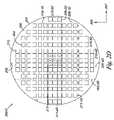
- FIG. 1illustrates a prior art top view of a semiconductor wafer.
- FIGS. 2A-2Dillustrate top views of semiconductor wafers processed according to one or more embodiments of the present disclosure.
- FIGS. 3A-3Dillustrate cross-sectional side views of segments of a semiconductor wafer processed according to one or more embodiments of the present disclosure.
- FIGS. 4A-4Cillustrate cross-sectional side views of segments of a semiconductor wafer processed according to one or more embodiments of the present disclosure.
- FIGS. 5A-5Fillustrate cross-sectional side views of segments of a semiconductor wafer processed according to one or more embodiments of the present disclosure.
- One embodimentincludes removing portions of a first side of the semiconductor wafer to form a number of trenches of a particular depth in rows and columns.
- the methodfurther includes forming a passivation layer on side walls of the number of trenches.
- the methodalso includes cutting a second side of the semiconductor wafer in rows and columns aligned with the number of trenches such that the semiconductor wafer singulates into a number of dice.
- waferand “substrate” are used interchangeably and are to be understood as including, but not limited to, silicon-on-insulator (SOI) or silicon-on-sapphire (SOS) technology, doped and undoped semiconductors, epitaxial layers of silicon supported by a base semiconductor foundation, and other semiconductor structures.
- SOIsilicon-on-insulator
- SOSsilicon-on-sapphire
- doped and undoped semiconductorsdoped and undoped semiconductors
- epitaxial layers of silicon supported by a base semiconductor foundationand other semiconductor structures.
- previous process stepsmay have been utilized to form regions or junctions in the base semiconductor structure or foundation.
- FIG. 1illustrates a prior art top view of a semiconductor wafer 100 .
- the wafer 100can have a round peripheral edge 101 .
- the wafer 100can include a number of dice 103 having streets 105 located therebetween.
- streets 105may be referred to as saw streets or scribe streets, e.g., paths along which a tool may cut in order to singulate the dice 103 .
- the streets 105Prior to a cutting, the streets 105 may be etched to a particular depth to help guide a saw blade.
- one or more sidemarks 106 along the edge 101 of the top of the wafer 100can be used to align the saw blade before cutting. Although two sidemarks 106 are illustrated, a wafer 100 could include more or fewer sidemarks 106 .
- the wafer 100could include a sidemark 106 at the edge 101 of every street 105 .
- the dice 103can be formed on the wafer 100 such that the streets 105 are formed in perpendicular rows 107 and columns 109 .
- the streets 105 forming rows 107 and columns 109can have a same width 110 . That is, each of the streets 105 in each direction can be formed to the same width 110 .
- the dice 103can comprise electronic devices 113 .
- an electronic device 113can include transistors, capacitors, diodes, memory devices, processors, other devices, and/or integrated circuits.
- a testing circuit 111can include circuits for determining the functionality of one or more electronic devices 113 formed on the semiconductor wafer 100 .
- a testing circuit 111can include a contact pad for probing to determine whether one or more electronic devices 113 associated with the testing circuit 111 are functional.
- testing circuits 111are illustrated in only one row 107 , they can be formed in more than one street 105 , all streets 105 , or on portions of one or more streets 105 .
- testing circuits 111can be probed after formation of the electronic devices 113 and before the wafer 100 is diced. After a determination has been made as to which of the electronic devices 113 formed on the wafer 100 are functional, the wafer 100 can be diced, e.g., by a rotating saw blade cutting along the streets 105 , thereby destroying the testing circuits 111 , which may no longer serve a purpose.
- one or more rotating saw bladescan be used to singulate the dice 103 by cutting along the streets 105 .
- the saw bladecan enter the peripheral edge 101 of the wafer 100 at a blade entry point, e.g., a sidemark 106 , such that the blade is aligned with a particular street.
- a blade entry pointe.g., a sidemark 106
- the saw bladecan also contact side surfaces of the number of streets 105 , which may include side surfaces of electronic devices 113 when they are formed such that there is no substrate barrier between the electronic device 113 and the street.
- microcracks that may form in the side surface on the substratecan propagate into the electronic device 113 at least partially in response to mechanical, thermal, chemical, or other stresses that the wafer 100 may be subjected to during processing.
- microcracks and/or other damage to thin films and/or electronic devicesmay still occur near the boundary of the etched trenches using methods described in the '836 and/or '977 patents.
- Backgrinding and/or sawing from the backside of the semiconductor wafere.g., as the grinder and/or saw blade approach the trench, can contribute to cracking and/or other damage.
- Backgrinding a wafer with an open trenchcan cause stress and/or deformation along one or more of the trench walls. Such factors may damage one or more electronic devices formed on the wafer.
- Some methodsmay narrow the width of the saw streets, e.g., the width between electronic devices, to a point where they are too thin to support placement of testing circuits. Such methods may require placement of testing circuits on areas of the semiconductor wafer that could otherwise be used for the formation of electronic devices, thereby at least partially reducing one or more benefits of narrowing the saw street.
- FIGS. 2A-2Dillustrate top views of semiconductor wafers processed according to one or more embodiments of the present disclosure.
- Semiconductor wafers processed according to various embodiments described hereincan provide a greater number of dice, e.g., electronic devices, per wafer while reducing a likelihood of device failure due to processing conditions, e.g., dicing the wafer.
- Such embodimentscan retain an ability to test one or more electronic devices while reducing widths of certain streets between devices.
- FIG. 2Aillustrates a top view of a semiconductor wafer 200 -A processed according to one or more embodiments of the present disclosure.
- the wafer 200 -Acan be substantially similar to the wafer 100 processed according to some previous approaches, such as is illustrated in FIG. 1 . That is, the wafer 200 -A can have a round peripheral edge 201 with one or more sidemarks 206 , and have substantially similar dimensions to the wafer 100 illustrated in FIG. 1 .
- the wafer 200 -Acan, prior to processing, have a thickness between approximately 500-750 micrometers and a width of approximately eight inches ( ⁇ 200 millimeters). Drawings are not to scale.
- the wafer 200 -A illustrated in FIG. 2Acontains more dice 203 , e.g., chips, devices, etc., than the wafer 100 illustrated in FIG. 1 .
- the distance between the dice 203e.g., the width 210 of the streets 205
- Various methods for achieving reduced street 205 widths 210are described below in connection with FIGS. 3A-5F , e.g., by etching narrower trench rows and columns than can be cut by a saw blade.
- street 205 widths 210of approximately 25-50 micrometers, e.g., an approximate width of a saw blade used to singulate the dice 203 plus any buffer region around the saw street 205 .
- the top surface 202 of wafer 200 -Acan be etched between dice 203 to widths 210 between approximately 5-10 micrometers.
- each die 203may comprise a device, e.g., an electronic device 213 or a testing circuit 211 .
- testing circuits 211may be formed in the saw streets 205 prior to singulation. However, in embodiments where all saw streets 205 are reduced in width 210 , as illustrated in FIG. 2A , testing circuits 211 may be relocated to one or more dice 203 if the saw street 205 is too narrow to house such a testing circuit 211 .
- one die 203could comprise a testing circuit 211 capable of testing any of the eight dies 203 adjacent thereto. An example illustration of this appears in FIG. 2A as indicated by testing circuit 211 “T” surrounded by eight electronic devices 213 “E.” In such an example, one out of every nine dice 203 could be a testing circuit 211 rather than an electronic device 213 .
- forming electronic devices 213 according to a method where all streets 205 are reduced to a width 210 narrow enough that testing circuits 211 no longer fit in the saw streets 205can still provide a greater yield of a total number of electronic devices 213 per wafer 200 -A as long as the increased number of dice 203 per wafer 200 -A is great enough to account for the need to use certain dice 203 as testing circuits 211 .
- the increased number of dice 203 per wafer 200 -Ashould be greater than the number of dice 203 originally produced divided by the number of electronic devices 213 a single testing circuit 211 can test, assuming each device needs to be tested.
- FIG. 2Billustrates a top view of a semiconductor wafer 200 -B processed according to one or more embodiments of the present disclosure.
- the wafer 200 -Bcan be substantially similar to the wafer 200 -A described in connection with the embodiment illustrated in FIG. 2A prior to its processing.
- the wafer 200 -Bcan include one or more sidemarks 206 for aligning a saw blade. When cutting is performed from a backside of the wafer 200 -B, the saw blade can be aligned to sidemarks 206 on the front surface 202 of the wafer 200 -B.
- the wafer 200 -B illustrated in FIG. 2Bincludes more dice 203 than the wafer 100 illustrated in FIG. 1 , but fewer than the wafer 200 -A illustrated in FIG. 2A .
- the wafer 200 -B illustrated in FIG. 2Bincludes narrower streets 205 - 2 in the horizontal direction 207 , e.g., trench rows, than streets 205 - 1 the vertical direction 209 , e.g., trench columns.
- the trench rowscan be etched to a width 210 - 2 of approximately 5-10 micrometers, while the trench columns can be etched to a width 210 - 1 sufficient to house a testing circuit 211 , e.g., greater than 25 micrometers.
- the wafer 200 -Bhas a circular edge 201 , it is not critical which direction is defined as vertical 209 (column) or horizontal 207 (row) as long as the two directions are perpendicular to each other.
- the embodiment illustrated in FIG. 2Balso includes a number of testing circuits 211 located in the vertical streets 205 - 1 , e.g., trench columns.
- a testing circuit 211can be formed adjacent to each die 203 , or spaced differently depending on the characteristics of the particular testing circuit 211 .
- a single testing circuit 211may be designed to test one die 203 , e.g., electronic device 213 , or more than one die.
- One of ordinary skill in the art having read and understood the present disclosurewill understand an appropriate placement scheme for testing circuits 211 based on their characteristics.
- 2Bcan provide a greater number of dice 203 housing electronic devices 213 per wafer 200 -B than some previous approaches, while simultaneously allowing the placement of testing circuits 213 in the saw streets, e.g., not placing testing circuits on a die 203 .
- FIG. 2Cillustrates a top view of a semiconductor wafer 200 -C processed according to one or more embodiments of the present disclosure.
- the wafer 200 -Ccan include one or more sidemarks 206 for saw blade alignment.
- a sidemark 206can be used for alignment with one or more, or even all, streets in each direction.
- sidemarks 206 on a top surface 202e.g., front side, of a wafer 200 -C can be used for aligning a saw blade for cutting from the backside of the wafer 200 -C.
- Other methods of saw blade alignmentcan be used with the various embodiments of the present disclosure including, but not limited to, optical, infra-red, laser, and others as will be known to one of ordinary skill in the art.
- every other trench row and columne.g., vertical 209 and horizontal 207 streets, starting from the center and radiating out, are etched to a greater width than the alternating trench rows and columns.
- the narrower streets 205 - 2 C and 205 - 4 Ccan be etched to approximately 5-10 micrometers in width 210 - 2 C and 210 - 4 C
- the wider streets 205 - 1 C and 205 - 3 Ccan be etched to a width 210 - 1 C and 210 - 3 C greater than approximately 25 micrometers to allow for the placement of one or more testing circuits therein.
- the width 210 - 1 C of the wider horizontal streets 250 - 1 Cdoes not necessarily have to be the same as the width 210 - 3 C of the wider vertical streets 205 - 3 C.
- the width 210 - 2 C of the narrower horizontal streets 205 - 2 Cdoes not have to be the same as the width 210 - 4 C of the narrower vertical streets 205 - 4 C.
- Testing circuits 211 - 1can be formed, e.g., placed, adjacent to one or more dice 203 on the wider streets, e.g., streets 205 - 1 C and 205 - 3 C.
- the testing circuits 211 - 2can be placed at the intersections of the wider streets, e.g., streets 205 - 1 C and 205 - 30 , forming four “corner-posts” around a group of four dice 303 .
- One of ordinary skill in the art, having read and understood the present disclosurewill appreciate additional testing circuit placement schemes, which will not deviate from the scope of this disclosure.
- testing circuitsmay be placed on dice 203 , streets, e.g., street 205 - 1 , or a combination thereof.
- FIG. 2Dillustrates a top view of a semiconductor wafer 200 -D processed according to one or more embodiments of the present disclosure.
- the wafer 200 -DPrior to processing the wafer 200 -D can be substantially similar to wafers described above prior to their processing.
- the wafercan have a round peripheral edge 201 and one or more sidemarks 206 on a top, e.g., front, surface 202 .
- the embodiment illustrated in FIG. 2Dincludes streets of varying widths in the horizontal 207 and vertical 209 directions. Streets, e.g., street 205 - 4 D, formed near the center of the wafer in columns have a relatively narrow width 210 - 4 D compared to streets, e.g., street 205 - 3 D formed closer to the edges of the wafer in columns with a relatively wide width 210 - 3 D. Likewise, streets, e.g., street 205 - 2 D, formed near the center of the wafer in rows have a relatively narrow width 210 - 2 D compared to streets, e.g., street 205 - 1 D formed closer to the edges of the wafer in rows with a relatively wide width 210 - 1 D. For example, streets formed to the narrower width may be etched to a width between approximately 5-10 micrometers, while streets formed to the wider width may have a width greater than approximately 25 micrometers.
- the wafer 200 -Dcan have a number of dice 203 formed on the top surface 202 as electronic devices 213 and/or testing circuits, e.g., testing circuit 211 - 2 D.
- Testing circuitse.g., testing circuit 211 - 1 D, may be formed in the streets between dice 203 .
- testing circuits formed in streetscan be formed in streets having relatively wider widths, while testing circuits formed on a die can be formed on die surrounded by streets having relatively narrower widths.
- testing circuitssufficient to test each electronic device
- more testing devicesmay be formed in streets between dice closer to the edges of the wafer, as opposed to dice formed near the center of the wafer.
- Such embodimentsmay be useful for wafer used to form electronic devices known to have a higher average yield in certain areas of the wafer, e.g., near the center of the wafer. That is, such embodiments can allow for a greater number of dice, e.g., electronic devices, to be formed in areas of the wafer that tend to produce higher yields, e.g., devices that do not fail, on average.
- Embodimentsare not limited to arranging street widths such that they are narrower in the center of the wafer, other portions of the wafer, e.g., other portions that may produce a higher yield on average, may be selected to produce a greater number of dice by adjusting street widths accordingly, as will be appreciated by one of ordinary skill in the art having read and understood the present disclosure.
- FIGS. 3A-3Dillustrate cross-sectional side views of segments of a semiconductor wafer processed according to one or more embodiments of the present disclosure.
- the processes illustrated in FIGS. 3A-3Dcan function to provide an additional barrier to microcrack propagation near electronic devices.
- Such embodimentscan be process efficient because many electronic devices have a passivation layer applied as one of the process steps during formation. Therefore applying the passivation layer as a barrier between saw streets and electronic devices can be achieved using a common process step with device formation.
- FIG. 3Aillustrates a cross-sectional view of a segment 320 -A of a semiconductor substrate, e.g., bulk silicon, having a top surface 302 , e.g., a front side of the wafer, and a bottom surface 304 , e.g., a backside of the wafer.
- the segment 320 -A of the semiconductor substrateis illustrated including a first device 315 - 1 and a second device 315 - 2 formed proximate to the top surface 302 , e.g., front side of the wafer, according to a previous process that will be understood by one of ordinary skill in the art.
- the devicesmay comprise electronic devices and/or testing circuits.
- the segment 320 -A of semiconductor substrateis illustrated with a portion removed from the top surface 302 , e.g., from the front side of the wafer when viewed from a top view, that forms a narrow trench 322 , e.g., having a width 310 of approximately 5-10 micrometers, to a particular depth 324 , e.g., approximately 30-60 micrometers from the top surface 302 . That is, a length of a trench sidewall, e.g., sidewall 330 in FIG. 3B , can be between approximately 30-60 micrometers. Embodiments are not so limited. As illustrated in FIG.
- the trench 322can extend between the first device 315 - 1 and second device 315 - 2 to a depth 324 greater than the depth 326 of the electronic and/or testing circuits, e.g., devices 315 - 1 and 315 - 2 .
- the portioncan be removed, for example, by anisotropically dry etching the semiconductor wafer, e.g., by plasma etching, reactive ion etching, or other methods.
- Etch chemistriescan include SF 6 /O 2 /HBr, SF 6 /C 4 F 8 /HBr, or other chemistries as will be understood by one of ordinary skill in the art.
- a photoresist maskmay be formed over areas of the wafer desired to be protected from the etching process.
- etches in the semiconductor wafercan extend along the length of each street, forming perpendicular rows and columns on the front side of the wafer, e.g., as illustrated in FIG. 2A .
- FIG. 3Billustrates a cross-sectional view of a segment 320 -B of the semiconductor substrate, e.g., segment 320 -A illustrated in FIG. 3A , at a subsequent processing point.
- a passivation layer 328can be formed on the side walls 330 and bottom 332 of the trenches 322 , as well as over the devices 315 - 1 and 315 - 2 , e.g., electronic and/or testing circuits.
- the same passivation layer 328can be used to coat the trench 322 and to passivate the electronic device, e.g., a transistor. Accordingly, a single processing step can be employed to reduce fabrication cost and time.
- coating the trench 322 with a passivation layer 328can provide additional protection against the formation of microcracks beyond the trench wall that may propagate near the devices 315 - 1 and 315 - 2 .
- Microcracksmay result from planarizing, e.g., backgrinding, and/or cutting the wafer.
- stresses to the material from the saw and/or grindercan travel along trench walls.
- a microcrack traveling through the passivation layer 328is less likely to transition across a barrier formed at the intersection of different materials, e.g., bulk silicon and the passivation layer 328 and/or some components of the electronic devices 315 - 1 and 315 - 2 and the passivation layer 328 .
- such microcrackscan contribute to failure or reduced functionality of one or more devices, e.g., device 315 - 1 , formed on the semiconductor wafer.
- the passivation layer 328can be formed as silicon nitride (SiN), silicon oxynitride (SiON), titanium nitride (TiN), or another passivating material as will be understood by one of ordinary skill in the art.
- the passivation layer 328can be formed by methods such as chemical vapor deposition, pulsed laser deposition, sputter deposition, atomic layer deposition, and molecular beam epitaxy, among other methods.
- FIG. 3Cillustrates a cross-sectional view of a segment 320 -C of the semiconductor substrate, e.g., segment 320 -B illustrated in FIG. 3B , at a subsequent processing point.
- the bottom 304 - 1e.g., backside
- CMPchemical mechanical polishing/planarization
- a protective layermay be applied to the wafer to protect the previously formed devices. In one or more embodiments using the processes illustrated in FIGS.
- the semiconductor wafercan be thinned 334 such that a particular thickness 336 of substrate remains between the bottom 332 of the trenches 322 and the backside 304 - 2 (after thinning) of the wafer.
- the particular thickness 336 remaining after thinninge.g., backgrinding, can help to provide electrical and physical isolation for electronic devices, e.g., devices 315 - 1 and 315 - 2 , formed on the wafer.
- FIG. 3Dillustrates a cross-sectional view of a segment 320 -D of the semiconductor substrate, e.g., segment 320 -B illustrated in FIG. 3B , at a subsequent processing point.
- the processing step illustrated in FIG. 3De.g., cutting 335 -D the wafer, can occur after the processing step illustrated in FIG. 3B , e.g., after forming a passivation layer 328 on the wafer. Such an embodiment is illustrated in FIG. 3D at cut 335 -D.
- the processing step illustrated in FIG. 3Dcan occur after the processing step illustrated in FIG. 3C , e.g., after thinning 334 the wafer. Such an embodiment is illustrated in FIG. 3C at cut 335 -C.
- a backside 304 of the semiconductor wafercan be cut 335 -D, e.g., with a rotating wafer saw, to the bottom 332 of the trench 322 .
- the wafercan be cut in rows and columns aligned with the number of trenches such that the semiconductor wafer singluates into a number of dice, e.g., where a die includes a device, e.g., an electronic device such as devices 315 - 1 and 315 - 2 . Accordingly, the saw blade does not contact a surface of the substrate adjacent to the devices, e.g., trench side walls 330 .
- any microcracks that may form in the wafer because of the rotating saw bladeare less likely to propagate to an area where they would be likely to affect the functionality of the devices 315 - 1 and 315 - 2 .
- the passivation layer 328can act as a barrier between the microcracks and the devices 315 - 1 and 315 - 2 by absorbing the microcracks and helping to prevent transition thereof into the electronic devices, e.g., devices 315 - 1 and 315 - 2 .
- FIGS. 4A-4Cillustrate cross-sectional side views of segments of a semiconductor wafer processed according to one or more embodiments of the present disclosure.
- the processes illustrated in FIGS. 4A-4Ccan function to singulate a semiconductor wafer into a number of dice without the use of a rotating saw blade, backgrinder, or polisher on a surface of the wafer opposed to an open trench.
- Such embodimentscan be useful to reduce or eliminate the loss of device functionality due to microcrack propagation or other damage to electronic devices adjacent to one or more trenches.
- FIG. 4Aillustrates a cross-sectional view of a segment 420 -A of a semiconductor substrate, e.g., bulk silicon, having a top surface 402 , e.g., a front side of the wafer, and a bottom surface 404 , e.g., a backside of the wafer.
- the segment 420 -A of the semiconductor substrateis illustrated including a first device 415 - 1 and a second device 415 - 2 formed proximate to the top surface 402 , e.g., front side of the wafer, according to a process that will be understood by one of ordinary skill in the art.
- the devices 415 - 1 and 415 - 2may comprise electronic devices or testing circuits.
- FIG. 4Billustrates a cross-sectional view of a segment 420 -B of the semiconductor substrate, e.g., segment 420 -A illustrated in FIG. 4A , at a subsequent processing point.
- the backside 404 - 1 (before thinning), e.g., bottom, of the wafercan be thinned 434 , e.g., through mechanical backgrinding, chemical etching, mechanical polishing, and/or chemical mechanical polishing, to a second backside 404 - 2 (after thinning).
- a protective layermay be applied to the wafer to protect the previously formed devices 415 - 1 and 415 - 2 .
- the semiconductor waferPrior to device formation and thinning 434 , the semiconductor wafer can have an initial thickness 438 between 500-750 micrometers. For example, the wafer may be thinned 434 to a final thickness 440 between 100-300 micrometers. Embodiments are not so limited.
- FIG. 4Cillustrates a cross-sectional view of a segment 420 -C of the semiconductor substrate, e.g., segment 420 -B illustrated in FIG. 4B , at a subsequent processing point.
- a top surface 402e.g., a front side of the wafer
- the wafercan be etched in a number of rows and columns between the electronic devices.
- this processing stepcan etch from a top surface 402 , e.g., a front side of the wafer, through to a bottom surface 404 - 2 , e.g., a backside of the wafer.
- a trench 422 formed by etchingcan pass completely through the wafer so as to singulate the wafer into a number of dice corresponding to a number of devices 415 - 1 and 415 - 2 .
- Such embodimentshave an additional advantage over some previous approaches that etch trenches 422 before wafer thinning 434 because such embodiments backgrind to a thickness substantially equivalent to the depth 424 of the trenches 422 .
- Such previous approachescan allow transfer of vibrations and physical stress along the trench side walls 430 to the edge of the devices 415 - 1 and 415 - 2 when the grinder is in close proximity to the bottom 432 of the trench 422 , potentially affecting the functionality of the devices 415 - 1 and 415 - 2 .
- the above described embodiments of the present disclosurethin 434 the wafer before etching, which allows a backgrinder to stop a substantial distance, e.g., distance 442 , e.g., more than 40 micrometers, from the devices 415 - 1 and 415 - 2 without transferring energy along a previously formed trench side walls 430 .
- one or more test circuitscan be placed, prior to etching, proximate to the top surface 402 , e.g., front side, of the semiconductor wafer thereby allowing testing of a number of electronic devices, e.g., devices 415 - 1 and 415 - 2 , previously formed on the wafer.
- FIGS. 5A-5Fillustrate cross-sectional side views of segments of a semiconductor wafer processed according to one or more embodiments of the present disclosure.
- the processes illustrated in FIGS. 5A-5Fcan function to singulate a semiconductor wafer into a number of dice without the use of a rotating saw blade, while providing trenches filled with a material that can act as a stress buffer while the wafer is being thinned. Subsequently, the filler material can be removed to singulate the dice.
- Such embodimentscan be useful to reduce or eliminate the loss of device functionality due to microcrack propagation or other damage to electronic devices adjacent to one or more trenches.
- FIG. 5Aillustrates a cross-sectional view of a segment 520 -A of a semiconductor substrate, e.g., bulk silicon, having a top surface 502 , e.g., a front side of the wafer, and a bottom surface 504 , e.g., a backside of the wafer.
- the segment 520 -A of the semiconductor substrateis illustrated including a first device 515 - 1 and a second device 515 - 2 formed proximate to the top surface 502 , e.g., front side, of the wafer according to a process that will be understood by one of ordinary skill in the art.
- the devices 515 - 1 and 515 - 2may comprise electronic and/or testing circuits.
- FIG. 5Billustrates a cross-sectional view of a segment 520 -B of the semiconductor substrate, e.g., segment 520 -A illustrated in FIG. 5A , at a subsequent processing point.
- a trench 522can be etched into the top surface 502 , e.g., front side, of the semiconductor wafer. As illustrated in FIG. 5B , the trench 522 can extend to a depth 524 greater than the depth 526 of the electronic and/or testing circuit.
- the trench 522can be etched to a depth 524 between approximately 30-60 micrometers from the top surface 502 of the wafer, e.g., where the top surface 502 can include the bulk wafer 550 and any additional layers, e.g., layers 551 and 552 , added prior to etching.
- the trench 522can be etched to a width 510 between approximately 5-10 micrometers.
- the devices 515 - 1 and 515 - 2can have a depth 526 between approximately 3-5 micrometers from the top surface 502 of the wafer, where the depth 526 of the device can include any layers, e.g., layers 551 and 552 , applied over the device, e.g., a passivation layer.
- the trench 522can be etched according to processes described above with respect to FIG. 3A or with other etching methods known to one of ordinary skill in the art. When viewed from a top view, etches in the semiconductor wafer can extend along the length of each street, forming perpendicular rows and columns on the front side 502 of the wafer.
- FIG. 5Cillustrates a cross-sectional view of a segment 520 -C of the semiconductor substrate, e.g., segment 520 -B illustrated in FIG. 5B , at a subsequent processing point.
- a polyimide layer 544 or resist layercan be deposited to fill the trenches 522 and cover the devices 515 - 1 and 515 - 2 , e.g., forming a uniform top surface 502 on the semiconductor wafer.
- the polyimide layer 544can serve as a stress buffer due to its shock resistant properties during later processing steps to help protect the devices 515 - 1 and 515 - 2 previously formed in the wafer.
- FIG. 5Dillustrates a cross-sectional view of a segment 520 -D of the semiconductor substrate, e.g., segment 520 -C illustrated in FIG. 50 , at a subsequent processing point.
- the backside 504 - 1 (before thinning), e.g., bottom, of the wafercan be thinned 534 to a second backside 504 - 2 (after thinning), e.g., through mechanical backgrinding, chemical etching, mechanical polishing, and/or chemical mechanical polishing.
- the backside 504 - 2(after thinning), e.g., bottom of the wafer, can be thinned to a point substantially equal to the bottom 532 of the polyimide 544 filled trench 522 .
- a protective layermay be applied to the wafer to protect the previously formed devices 515 - 1 and 515 - 2 .
- FIG. 5Eillustrates a cross-sectional view of a segment 520 -E of the semiconductor substrate, e.g., segment 520 -D illustrated in FIG. 5D , at a subsequent processing point.
- a layer of adhesive material 546e.g., dicing tape
- the backside 504e.g., bottom
- the wafercan be released from the top 502 , e.g., front side.
- the layer of adhesive material 526can support the devices 515 - 1 and 515 - 2 during later processing points.
- FIG. 5Fillustrates a cross-sectional view of a segment 520 -F of the semiconductor substrate, e.g., segment 520 -E illustrated in FIG. 5E , at a subsequent processing point.
- the polyimide layer 544can be removed 548 , e.g., wet removal.
- the polyimide layer 544can be removed 548 through application of an acid such as sulfuric acid.
- Another example of a method to remove 548 the polyimide layer 544is with a frequency-based energy source, e.g., ultrasonic energy, provided in U.S. Pat. No. 5,925,260 to Jiang.
- a deionized water flushcan be performed to rinse away material remaining after the wet removal.
- the waferwill have been singulated into dice, e.g., devices 515 - 1 and 515 - 2 . Although the dice may still be attached to the layer of adhesive material 546 , e.g., dicing tape, the dice can be picked for packaging.
- One embodimentincludes removing portions of a first side of the semiconductor wafer to form a number of trenches of a particular depth in rows and columns.
- the methodfurther includes forming a passivation layer on side walls of the number of trenches.
- the methodalso includes cutting a second side of the semiconductor wafer in rows and columns aligned with the number of trenches such that the semiconductor wafer singulates into a number of dice.
Landscapes
- Engineering & Computer Science (AREA)
- Physics & Mathematics (AREA)
- Condensed Matter Physics & Semiconductors (AREA)
- General Physics & Mathematics (AREA)
- Manufacturing & Machinery (AREA)
- Computer Hardware Design (AREA)
- Microelectronics & Electronic Packaging (AREA)
- Power Engineering (AREA)
- Dicing (AREA)
Abstract
Description
- The present disclosure relates generally to electronic semiconductors and, more particularly, to processing semiconductor wafers.
- To form individual electronic devices from a semiconductor wafer, various electronic circuitry can be formed on a front side of the semiconductor wafer. The electronic devices can be arranged in a grid-like pattern on the semiconductor wafer. In order to separate, e.g., singulate, the devices, the semiconductor wafer can be diced by various means.
- One method of dicing a semiconductor wafer is to cut through the wafer from the front side, e.g., the side on which electronic devices are formed, with a rotating saw blade. However, using a saw blade in such a manner can have various processing limitations. For example, the width of the saw blade reduces the overall usable area of the semiconductor wafer. Furthermore, sawing through a semiconductor wafer can cause microcracks near the edge of the saw street, which may propagate and at least partially cause a failure for some electronic devices formed near the edges of saw streets.
- Some methods for semiconductor wafer processing include forming test circuits in areas of the wafer that will be used as saw streets during singulation. These testing circuits can be probed to help determine whether certain of the electronic devices formed on the wafer are functioning properly.
FIG. 1 illustrates a prior art top view of a semiconductor wafer.FIGS. 2A-2D illustrate top views of semiconductor wafers processed according to one or more embodiments of the present disclosure.FIGS. 3A-3D illustrate cross-sectional side views of segments of a semiconductor wafer processed according to one or more embodiments of the present disclosure.FIGS. 4A-4C illustrate cross-sectional side views of segments of a semiconductor wafer processed according to one or more embodiments of the present disclosure.FIGS. 5A-5F illustrate cross-sectional side views of segments of a semiconductor wafer processed according to one or more embodiments of the present disclosure.- Methods for processing semiconductor wafers are described herein. One embodiment includes removing portions of a first side of the semiconductor wafer to form a number of trenches of a particular depth in rows and columns. The method further includes forming a passivation layer on side walls of the number of trenches. The method also includes cutting a second side of the semiconductor wafer in rows and columns aligned with the number of trenches such that the semiconductor wafer singulates into a number of dice.
- In the following detailed description of the present disclosure, reference is made to the accompanying drawings that form a part hereof, and in which is shown by way of illustration how one or more embodiments of the disclosure may be practiced. These embodiments are described in sufficient detail to enable those of ordinary skill in the art to practice the embodiments of this disclosure, and it is to be understood that other embodiments may be utilized and that process, electrical, and/or structural changes may be made without departing from the scope of the present disclosure.
- As used in this disclosure, the terms “wafer” and “substrate” are used interchangeably and are to be understood as including, but not limited to, silicon-on-insulator (SOI) or silicon-on-sapphire (SOS) technology, doped and undoped semiconductors, epitaxial layers of silicon supported by a base semiconductor foundation, and other semiconductor structures. Furthermore, when reference is made to a “wafer” or “substrate” in the following description, previous process steps may have been utilized to form regions or junctions in the base semiconductor structure or foundation.
FIG. 1 illustrates a prior art top view of asemiconductor wafer 100. As illustrated inFIG. 1 , thewafer 100 can have a roundperipheral edge 101. Thewafer 100 can include a number ofdice 103 havingstreets 105 located therebetween. As used herein,streets 105 may be referred to as saw streets or scribe streets, e.g., paths along which a tool may cut in order to singulate thedice 103. Prior to a cutting, thestreets 105 may be etched to a particular depth to help guide a saw blade. Furthermore, one ormore sidemarks 106 along theedge 101 of the top of thewafer 100 can be used to align the saw blade before cutting. Although twosidemarks 106 are illustrated, awafer 100 could include more orfewer sidemarks 106. For example, thewafer 100 could include asidemark 106 at theedge 101 of everystreet 105.- In many cases, and as shown in
FIG. 1 , thedice 103 can be formed on thewafer 100 such that thestreets 105 are formed inperpendicular rows 107 andcolumns 109. As illustrated inFIG. 1 , according to some previous approaches, thestreets 105 formingrows 107 andcolumns 109 can have asame width 110. That is, each of thestreets 105 in each direction can be formed to thesame width 110. - The
dice 103 can compriseelectronic devices 113. As used herein, anelectronic device 113 can include transistors, capacitors, diodes, memory devices, processors, other devices, and/or integrated circuits. Atesting circuit 111, as used herein, can include circuits for determining the functionality of one or moreelectronic devices 113 formed on thesemiconductor wafer 100. For example, atesting circuit 111 can include a contact pad for probing to determine whether one or moreelectronic devices 113 associated with thetesting circuit 111 are functional. Althoughtesting circuits 111 are illustrated in only onerow 107, they can be formed in more than onestreet 105, allstreets 105, or on portions of one ormore streets 105. Thesetesting circuits 111 can be probed after formation of theelectronic devices 113 and before thewafer 100 is diced. After a determination has been made as to which of theelectronic devices 113 formed on thewafer 100 are functional, thewafer 100 can be diced, e.g., by a rotating saw blade cutting along thestreets 105, thereby destroying thetesting circuits 111, which may no longer serve a purpose. - In various previous wafer processing approaches, one or more rotating saw blades can be used to singulate the
dice 103 by cutting along thestreets 105. In such approaches, the saw blade can enter theperipheral edge 101 of thewafer 100 at a blade entry point, e.g., asidemark 106, such that the blade is aligned with a particular street. As the saw blade dices thewafer 100, it can make contact with atop surface 102 of thewafer 100. The saw blade can also contact side surfaces of the number ofstreets 105, which may include side surfaces ofelectronic devices 113 when they are formed such that there is no substrate barrier between theelectronic device 113 and the street. For processing methods including a substrate barrier between theelectronic devices 113 and thesaw street 105, microcracks that may form in the side surface on the substrate can propagate into theelectronic device 113 at least partially in response to mechanical, thermal, chemical, or other stresses that thewafer 100 may be subjected to during processing. - An example of a previous approach to reduce the amount of semiconductor wafer dedicated to saw streets and mitigate the potential for damage from microcracks is described in U.S. Pat. No. 6,890,836 to Howard et al. The '836 patent appears to describe a method to etch trench streets in the front side of a semiconductor wafer and then singulate by cutting from the backside of the wafer to the bottom of the trenches. Another method that appears to be described in the '836 patent avoids the use of a saw altogether by etching trench streets in the front side of a wafer, then backgrinding to singulate the dice.
- Another example of a previous approach to reduce the width of saw streets is described in U.S. Pat. No. 7,052,977 to Yegnashankaran et al. The '977 patent appears to describe a method of dicing a semiconductor wafer by at least etching a number of trenches in the top surface of the wafer, then thinning the bottom surface until the wafer singulates into dice. The '977 patent teaches that the etch forms street openings that vertically weaken the wafer along a stress line extending from the street region vertically down towards the bottom surface of the wafer.
- However, microcracks and/or other damage to thin films and/or electronic devices may still occur near the boundary of the etched trenches using methods described in the '836 and/or '977 patents. Backgrinding and/or sawing from the backside of the semiconductor wafer, e.g., as the grinder and/or saw blade approach the trench, can contribute to cracking and/or other damage. Backgrinding a wafer with an open trench can cause stress and/or deformation along one or more of the trench walls. Such factors may damage one or more electronic devices formed on the wafer.
- Some methods, like the '836 patent describe above, may narrow the width of the saw streets, e.g., the width between electronic devices, to a point where they are too thin to support placement of testing circuits. Such methods may require placement of testing circuits on areas of the semiconductor wafer that could otherwise be used for the formation of electronic devices, thereby at least partially reducing one or more benefits of narrowing the saw street.
FIGS. 2A-2D illustrate top views of semiconductor wafers processed according to one or more embodiments of the present disclosure. Semiconductor wafers processed according to various embodiments described herein can provide a greater number of dice, e.g., electronic devices, per wafer while reducing a likelihood of device failure due to processing conditions, e.g., dicing the wafer. Such embodiments can retain an ability to test one or more electronic devices while reducing widths of certain streets between devices.FIG. 2A illustrates a top view of a semiconductor wafer200-A processed according to one or more embodiments of the present disclosure. Prior to processing, the wafer200-A can be substantially similar to thewafer 100 processed according to some previous approaches, such as is illustrated inFIG. 1 . That is, the wafer200-A can have a roundperipheral edge 201 with one or more sidemarks206, and have substantially similar dimensions to thewafer 100 illustrated inFIG. 1 . For example, the wafer200-A can, prior to processing, have a thickness between approximately 500-750 micrometers and a width of approximately eight inches (˜200 millimeters). Drawings are not to scale.- As can be seen from a comparison of
FIG. 2A withFIG. 1 , the wafer200-A illustrated inFIG. 2A containsmore dice 203, e.g., chips, devices, etc., than thewafer 100 illustrated inFIG. 1 . The distance between thedice 203, e.g., thewidth 210 of thestreets 205, has been decreased for allstreets 205 in both vertical209 and horizontal207 orientations. Various methods for achieving reducedstreet 205widths 210 are described below in connection withFIGS. 3A-5F , e.g., by etching narrower trench rows and columns than can be cut by a saw blade. Some previous approaches, such as that illustrated inFIG. 1 , includestreet 205widths 210 of approximately 25-50 micrometers, e.g., an approximate width of a saw blade used to singulate thedice 203 plus any buffer region around thesaw street 205. In contrast, thetop surface 202 of wafer200-A can be etched betweendice 203 towidths 210 between approximately 5-10 micrometers. - In the embodiment illustrated in
FIG. 2A , each die203 may comprise a device, e.g., anelectronic device 213 or atesting circuit 211. In some embodiments,testing circuits 211 may be formed in thesaw streets 205 prior to singulation. However, in embodiments where all sawstreets 205 are reduced inwidth 210, as illustrated inFIG. 2A ,testing circuits 211 may be relocated to one ormore dice 203 if thesaw street 205 is too narrow to house such atesting circuit 211. For example, one die203 could comprise atesting circuit 211 capable of testing any of the eight dies203 adjacent thereto. An example illustration of this appears inFIG. 2A as indicated bytesting circuit 211 “T” surrounded by eightelectronic devices 213 “E.” In such an example, one out of every ninedice 203 could be atesting circuit 211 rather than anelectronic device 213. - Therefore, forming
electronic devices 213 according to a method where allstreets 205 are reduced to awidth 210 narrow enough that testingcircuits 211 no longer fit in thesaw streets 205 can still provide a greater yield of a total number ofelectronic devices 213 per wafer200-A as long as the increased number ofdice 203 per wafer200-A is great enough to account for the need to usecertain dice 203 astesting circuits 211. Generally, the increased number ofdice 203 per wafer200-A should be greater than the number ofdice 203 originally produced divided by the number of electronic devices213 asingle testing circuit 211 can test, assuming each device needs to be tested. This can be represented by the equation: y>x/q, where y is the increased number ofdice 203, x is the original number ofdice 203, and q is the number ofelectronic devices 213 that asingle testing circuit 211 can test. In the example above, where asingle testing circuit 211 can test eight electronic devices, the result is that the number ofdice 203 should be increased by ⅛ (˜12.5%). Embodiments are not so limited. Asingle testing circuit 211 located on adie 203 could be used to test more or fewerelectronic devices 213 located onother dice 203. FIG. 2B illustrates a top view of a semiconductor wafer200-B processed according to one or more embodiments of the present disclosure. Prior to processing, the wafer200-B can be substantially similar to the wafer200-A described in connection with the embodiment illustrated inFIG. 2A prior to its processing. For example, the wafer200-B can include one or more sidemarks206 for aligning a saw blade. When cutting is performed from a backside of the wafer200-B, the saw blade can be aligned to sidemarks206 on thefront surface 202 of the wafer200-B.- The wafer200-B illustrated in
FIG. 2B includesmore dice 203 than thewafer 100 illustrated inFIG. 1 , but fewer than the wafer200-A illustrated inFIG. 2A . The wafer200-B illustrated inFIG. 2B includes narrower streets205-2 in thehorizontal direction 207, e.g., trench rows, than streets205-1 thevertical direction 209, e.g., trench columns. For example, the trench rows can be etched to a width210-2 of approximately 5-10 micrometers, while the trench columns can be etched to a width210-1 sufficient to house atesting circuit 211, e.g., greater than 25 micrometers. As one of ordinary skill in the art will appreciate, as the wafer200-B has acircular edge 201, it is not critical which direction is defined as vertical209 (column) or horizontal207 (row) as long as the two directions are perpendicular to each other. - The embodiment illustrated in
FIG. 2B also includes a number oftesting circuits 211 located in the vertical streets205-1, e.g., trench columns. Atesting circuit 211 can be formed adjacent to each die203, or spaced differently depending on the characteristics of theparticular testing circuit 211. For example, asingle testing circuit 211 may be designed to test onedie 203, e.g.,electronic device 213, or more than one die. One of ordinary skill in the art having read and understood the present disclosure will understand an appropriate placement scheme fortesting circuits 211 based on their characteristics. Semiconductor wafers processed, e.g., singulated or diced, according to the embodiment illustrated inFIG. 2B can provide a greater number ofdice 203 housingelectronic devices 213 per wafer200-B than some previous approaches, while simultaneously allowing the placement oftesting circuits 213 in the saw streets, e.g., not placing testing circuits on adie 203. FIG. 2C illustrates a top view of a semiconductor wafer200-C processed according to one or more embodiments of the present disclosure. Prior to processing the wafer200-C can be substantially similar to wafers described above inFIGS. 1-2B , prior to their processing. The wafer200-C can include one or more sidemarks206 for saw blade alignment. Asidemark 206 can be used for alignment with one or more, or even all, streets in each direction. As noted above,sidemarks 206 on atop surface 202, e.g., front side, of a wafer200-C can be used for aligning a saw blade for cutting from the backside of the wafer200-C. Other methods of saw blade alignment can be used with the various embodiments of the present disclosure including, but not limited to, optical, infra-red, laser, and others as will be known to one of ordinary skill in the art.- In the embodiment illustrated in
FIG. 2C , every other trench row and column, e.g., vertical209 and horizontal207 streets, starting from the center and radiating out, are etched to a greater width than the alternating trench rows and columns. For example, the narrower streets205-2C and205-4C can be etched to approximately 5-10 micrometers in width210-2C and210-4C, while the wider streets205-1C and205-3C can be etched to a width210-1C and210-3C greater than approximately 25 micrometers to allow for the placement of one or more testing circuits therein. However, the width210-1C of the wider horizontal streets250-1C does not necessarily have to be the same as the width210-3C of the wider vertical streets205-3C. Likewise, the width210-2C of the narrower horizontal streets205-2C does not have to be the same as the width210-4C of the narrower vertical streets205-4C. - Testing circuits211-1 can be formed, e.g., placed, adjacent to one or
more dice 203 on the wider streets, e.g., streets205-1C and205-3C. Alternatively, the testing circuits211-2 can be placed at the intersections of the wider streets, e.g., streets205-1C and205-30, forming four “corner-posts” around a group of four dice303. One of ordinary skill in the art, having read and understood the present disclosure will appreciate additional testing circuit placement schemes, which will not deviate from the scope of this disclosure. The embodiment illustrated inFIG. 2C provides additional options for processing semiconductor wafers, e.g., singulating or dicing, for yielding a greater number ofdice 203 housingelectronic devices 213 per wafer200-C than some previous approaches, while simultaneously allowing the placement of testing circuits, e.g., testing circuit211-1, in the saw streets, e.g., as opposed to placing testing circuits on adie 203. However, according to embodiments described herein, testing circuits may be placed ondice 203, streets, e.g., street205-1, or a combination thereof. FIG. 2D illustrates a top view of a semiconductor wafer200-D processed according to one or more embodiments of the present disclosure. Prior to processing the wafer200-D can be substantially similar to wafers described above prior to their processing. For example, the wafer can have a roundperipheral edge 201 and one or more sidemarks206 on a top, e.g., front,surface 202.- The embodiment illustrated in
FIG. 2D includes streets of varying widths in the horizontal207 and vertical209 directions. Streets, e.g., street205-4D, formed near the center of the wafer in columns have a relatively narrow width210-4D compared to streets, e.g., street205-3D formed closer to the edges of the wafer in columns with a relatively wide width210-3D. Likewise, streets, e.g., street205-2D, formed near the center of the wafer in rows have a relatively narrow width210-2D compared to streets, e.g., street205-1D formed closer to the edges of the wafer in rows with a relatively wide width210-1D. For example, streets formed to the narrower width may be etched to a width between approximately 5-10 micrometers, while streets formed to the wider width may have a width greater than approximately 25 micrometers. - The wafer200-D can have a number of
dice 203 formed on thetop surface 202 aselectronic devices 213 and/or testing circuits, e.g., testing circuit211-2D. Testing circuits, e.g., testing circuit211-1D, may be formed in the streets betweendice 203. For example, testing circuits formed in streets can be formed in streets having relatively wider widths, while testing circuits formed on a die can be formed on die surrounded by streets having relatively narrower widths. - Although the embodiment illustrated in
FIG. 2D can include testing circuits sufficient to test each electronic device, more testing devices may be formed in streets between dice closer to the edges of the wafer, as opposed to dice formed near the center of the wafer. Such embodiments may be useful for wafer used to form electronic devices known to have a higher average yield in certain areas of the wafer, e.g., near the center of the wafer. That is, such embodiments can allow for a greater number of dice, e.g., electronic devices, to be formed in areas of the wafer that tend to produce higher yields, e.g., devices that do not fail, on average. Embodiments are not limited to arranging street widths such that they are narrower in the center of the wafer, other portions of the wafer, e.g., other portions that may produce a higher yield on average, may be selected to produce a greater number of dice by adjusting street widths accordingly, as will be appreciated by one of ordinary skill in the art having read and understood the present disclosure. FIGS. 3A-3D illustrate cross-sectional side views of segments of a semiconductor wafer processed according to one or more embodiments of the present disclosure. The processes illustrated inFIGS. 3A-3D can function to provide an additional barrier to microcrack propagation near electronic devices. Such embodiments can be process efficient because many electronic devices have a passivation layer applied as one of the process steps during formation. Therefore applying the passivation layer as a barrier between saw streets and electronic devices can be achieved using a common process step with device formation.FIG. 3A illustrates a cross-sectional view of a segment320-A of a semiconductor substrate, e.g., bulk silicon, having atop surface 302, e.g., a front side of the wafer, and abottom surface 304, e.g., a backside of the wafer. The segment320-A of the semiconductor substrate is illustrated including a first device315-1 and a second device315-2 formed proximate to thetop surface 302, e.g., front side of the wafer, according to a previous process that will be understood by one of ordinary skill in the art. In one or more embodiments, the devices may comprise electronic devices and/or testing circuits.- The segment320-A of semiconductor substrate is illustrated with a portion removed from the
top surface 302, e.g., from the front side of the wafer when viewed from a top view, that forms anarrow trench 322, e.g., having awidth 310 of approximately 5-10 micrometers, to aparticular depth 324, e.g., approximately 30-60 micrometers from thetop surface 302. That is, a length of a trench sidewall, e.g.,sidewall 330 inFIG. 3B , can be between approximately 30-60 micrometers. Embodiments are not so limited. As illustrated inFIG. 3A , thetrench 322 can extend between the first device315-1 and second device315-2 to adepth 324 greater than thedepth 326 of the electronic and/or testing circuits, e.g., devices315-1 and315-2. The portion can be removed, for example, by anisotropically dry etching the semiconductor wafer, e.g., by plasma etching, reactive ion etching, or other methods. Etch chemistries can include SF6/O2/HBr, SF6/C4F8/HBr, or other chemistries as will be understood by one of ordinary skill in the art. Prior to etching, a photoresist mask may be formed over areas of the wafer desired to be protected from the etching process. When viewed from a top view, etches in the semiconductor wafer can extend along the length of each street, forming perpendicular rows and columns on the front side of the wafer, e.g., as illustrated inFIG. 2A . FIG. 3B illustrates a cross-sectional view of a segment320-B of the semiconductor substrate, e.g., segment320-A illustrated inFIG. 3A , at a subsequent processing point. After portions of the substrate have been removed, e.g., etched, apassivation layer 328 can be formed on theside walls 330 andbottom 332 of thetrenches 322, as well as over the devices315-1 and315-2, e.g., electronic and/or testing circuits. In embodiments where the devices are electronic devices, thesame passivation layer 328 can be used to coat thetrench 322 and to passivate the electronic device, e.g., a transistor. Accordingly, a single processing step can be employed to reduce fabrication cost and time.- Furthermore, coating the
trench 322 with apassivation layer 328 can provide additional protection against the formation of microcracks beyond the trench wall that may propagate near the devices315-1 and315-2. Microcracks may result from planarizing, e.g., backgrinding, and/or cutting the wafer. In embodiments where a rotating wafer saw and/or backgrinder approach atrench 322, stresses to the material from the saw and/or grinder can travel along trench walls. A microcrack traveling through thepassivation layer 328 is less likely to transition across a barrier formed at the intersection of different materials, e.g., bulk silicon and thepassivation layer 328 and/or some components of the electronic devices315-1 and315-2 and thepassivation layer 328. As described above, such microcracks can contribute to failure or reduced functionality of one or more devices, e.g., device315-1, formed on the semiconductor wafer. - The
passivation layer 328 can be formed as silicon nitride (SiN), silicon oxynitride (SiON), titanium nitride (TiN), or another passivating material as will be understood by one of ordinary skill in the art. Thepassivation layer 328 can be formed by methods such as chemical vapor deposition, pulsed laser deposition, sputter deposition, atomic layer deposition, and molecular beam epitaxy, among other methods. FIG. 3C illustrates a cross-sectional view of a segment320-C of the semiconductor substrate, e.g., segment320-B illustrated inFIG. 3B , at a subsequent processing point. After thepassivation layer 328 has been formed, the bottom304-1, e.g., backside, of the waver can be thinned334, e.g., through mechanical backgrinding, chemical etching, mechanical polishing, and/or chemical mechanical polishing/planarization (CMP). Prior to thinning, a protective layer may be applied to the wafer to protect the previously formed devices. In one or more embodiments using the processes illustrated inFIGS. 3A-3D , the semiconductor wafer can be thinned334 such that aparticular thickness 336 of substrate remains between the bottom332 of thetrenches 322 and the backside304-2 (after thinning) of the wafer. Theparticular thickness 336 remaining after thinning, e.g., backgrinding, can help to provide electrical and physical isolation for electronic devices, e.g., devices315-1 and315-2, formed on the wafer.FIG. 3D illustrates a cross-sectional view of a segment320-D of the semiconductor substrate, e.g., segment320-B illustrated inFIG. 3B , at a subsequent processing point. In one or more embodiments, the processing step illustrated inFIG. 3D , e.g., cutting335-D the wafer, can occur after the processing step illustrated inFIG. 3B , e.g., after forming apassivation layer 328 on the wafer. Such an embodiment is illustrated inFIG. 3D at cut335-D. In some embodiments, the processing step illustrated inFIG. 3D can occur after the processing step illustrated inFIG. 3C , e.g., after thinning334 the wafer. Such an embodiment is illustrated inFIG. 3C at cut335-C.- After the
passivation layer 328 has been formed, abackside 304 of the semiconductor wafer can be cut335-D, e.g., with a rotating wafer saw, to thebottom 332 of thetrench 322. From a bottom-view perspective, the wafer can be cut in rows and columns aligned with the number of trenches such that the semiconductor wafer singluates into a number of dice, e.g., where a die includes a device, e.g., an electronic device such as devices315-1 and315-2. Accordingly, the saw blade does not contact a surface of the substrate adjacent to the devices, e.g.,trench side walls 330. As a result, any microcracks that may form in the wafer because of the rotating saw blade are less likely to propagate to an area where they would be likely to affect the functionality of the devices315-1 and315-2. Furthermore, as described above with respect toFIG. 3B , if microcracks propagate in the portion of thepassivation layer 328 that coats thetrenches 322, e.g., due to contact with the saw blade, thepassivation layer 328 can act as a barrier between the microcracks and the devices315-1 and315-2 by absorbing the microcracks and helping to prevent transition thereof into the electronic devices, e.g., devices315-1 and315-2. FIGS. 4A-4C illustrate cross-sectional side views of segments of a semiconductor wafer processed according to one or more embodiments of the present disclosure. The processes illustrated inFIGS. 4A-4C can function to singulate a semiconductor wafer into a number of dice without the use of a rotating saw blade, backgrinder, or polisher on a surface of the wafer opposed to an open trench. Such embodiments can be useful to reduce or eliminate the loss of device functionality due to microcrack propagation or other damage to electronic devices adjacent to one or more trenches.FIG. 4A illustrates a cross-sectional view of a segment420-A of a semiconductor substrate, e.g., bulk silicon, having atop surface 402, e.g., a front side of the wafer, and abottom surface 404, e.g., a backside of the wafer. The segment420-A of the semiconductor substrate is illustrated including a first device415-1 and a second device415-2 formed proximate to thetop surface 402, e.g., front side of the wafer, according to a process that will be understood by one of ordinary skill in the art. In various embodiments, the devices415-1 and415-2 may comprise electronic devices or testing circuits.FIG. 4B illustrates a cross-sectional view of a segment420-B of the semiconductor substrate, e.g., segment420-A illustrated inFIG. 4A , at a subsequent processing point. After the devices415-1 and415-2 have been formed, the backside404-1 (before thinning), e.g., bottom, of the wafer can be thinned434, e.g., through mechanical backgrinding, chemical etching, mechanical polishing, and/or chemical mechanical polishing, to a second backside404-2 (after thinning). Prior to thinning, a protective layer may be applied to the wafer to protect the previously formed devices415-1 and415-2. Prior to device formation and thinning434, the semiconductor wafer can have aninitial thickness 438 between 500-750 micrometers. For example, the wafer may be thinned434 to afinal thickness 440 between 100-300 micrometers. Embodiments are not so limited.FIG. 4C illustrates a cross-sectional view of a segment420-C of the semiconductor substrate, e.g., segment420-B illustrated inFIG. 4B , at a subsequent processing point. After the wafer has been thinned434, atop surface 402, e.g., a front side of the wafer, can be etched between the electronic devices. From a top view perspective, the wafer can be etched in a number of rows and columns between the electronic devices. In one or more embodiments, this processing step can etch from atop surface 402, e.g., a front side of the wafer, through to a bottom surface404-2, e.g., a backside of the wafer. When the etching process occurs after thinning4341 atrench 422 formed by etching can pass completely through the wafer so as to singulate the wafer into a number of dice corresponding to a number of devices415-1 and415-2.- According to such embodiments, mechanical damage free die singulation is possible. Such embodiments have an additional advantage over some previous approaches that etch
trenches 422 before wafer thinning434 because such embodiments backgrind to a thickness substantially equivalent to thedepth 424 of thetrenches 422. Such previous approaches can allow transfer of vibrations and physical stress along thetrench side walls 430 to the edge of the devices415-1 and415-2 when the grinder is in close proximity to thebottom 432 of thetrench 422, potentially affecting the functionality of the devices415-1 and415-2. In contrast, the above described embodiments of the present disclosure thin434 the wafer before etching, which allows a backgrinder to stop a substantial distance, e.g.,distance 442, e.g., more than 40 micrometers, from the devices415-1 and415-2 without transferring energy along a previously formedtrench side walls 430. Additionally, one or more test circuits can be placed, prior to etching, proximate to thetop surface 402, e.g., front side, of the semiconductor wafer thereby allowing testing of a number of electronic devices, e.g., devices415-1 and415-2, previously formed on the wafer. FIGS. 5A-5F illustrate cross-sectional side views of segments of a semiconductor wafer processed according to one or more embodiments of the present disclosure. The processes illustrated inFIGS. 5A-5F can function to singulate a semiconductor wafer into a number of dice without the use of a rotating saw blade, while providing trenches filled with a material that can act as a stress buffer while the wafer is being thinned. Subsequently, the filler material can be removed to singulate the dice. Such embodiments can be useful to reduce or eliminate the loss of device functionality due to microcrack propagation or other damage to electronic devices adjacent to one or more trenches.FIG. 5A illustrates a cross-sectional view of a segment520-A of a semiconductor substrate, e.g., bulk silicon, having atop surface 502, e.g., a front side of the wafer, and abottom surface 504, e.g., a backside of the wafer. The segment520-A of the semiconductor substrate is illustrated including a first device515-1 and a second device515-2 formed proximate to thetop surface 502, e.g., front side, of the wafer according to a process that will be understood by one of ordinary skill in the art. In various embodiments, the devices515-1 and515-2 may comprise electronic and/or testing circuits.FIG. 5B illustrates a cross-sectional view of a segment520-B of the semiconductor substrate, e.g., segment520-A illustrated inFIG. 5A , at a subsequent processing point. After the devices515-1 and515-2 have been formed, atrench 522 can be etched into thetop surface 502, e.g., front side, of the semiconductor wafer. As illustrated inFIG. 5B , thetrench 522 can extend to adepth 524 greater than thedepth 526 of the electronic and/or testing circuit. For example, thetrench 522 can be etched to adepth 524 between approximately 30-60 micrometers from thetop surface 502 of the wafer, e.g., where thetop surface 502 can include thebulk wafer 550 and any additional layers, e.g., layers551 and552, added prior to etching. Thetrench 522 can be etched to awidth 510 between approximately 5-10 micrometers. The devices515-1 and515-2 can have adepth 526 between approximately 3-5 micrometers from thetop surface 502 of the wafer, where thedepth 526 of the device can include any layers, e.g., layers551 and552, applied over the device, e.g., a passivation layer. Thetrench 522 can be etched according to processes described above with respect toFIG. 3A or with other etching methods known to one of ordinary skill in the art. When viewed from a top view, etches in the semiconductor wafer can extend along the length of each street, forming perpendicular rows and columns on thefront side 502 of the wafer.FIG. 5C illustrates a cross-sectional view of a segment520-C of the semiconductor substrate, e.g., segment520-B illustrated inFIG. 5B , at a subsequent processing point. After thetrenches 522 have been formed, apolyimide layer 544 or resist layer can be deposited to fill thetrenches 522 and cover the devices515-1 and515-2, e.g., forming a uniformtop surface 502 on the semiconductor wafer. Thepolyimide layer 544 can serve as a stress buffer due to its shock resistant properties during later processing steps to help protect the devices515-1 and515-2 previously formed in the wafer.FIG. 5D illustrates a cross-sectional view of a segment520-D of the semiconductor substrate, e.g., segment520-C illustrated inFIG. 50 , at a subsequent processing point. After thepolyimide layer 544 has been deposited, the backside504-1 (before thinning), e.g., bottom, of the wafer can be thinned534 to a second backside504-2 (after thinning), e.g., through mechanical backgrinding, chemical etching, mechanical polishing, and/or chemical mechanical polishing. The backside504-2 (after thinning), e.g., bottom of the wafer, can be thinned to a point substantially equal to thebottom 532 of thepolyimide 544 filledtrench 522. Prior to thinning534, a protective layer may be applied to the wafer to protect the previously formed devices515-1 and515-2.FIG. 5E illustrates a cross-sectional view of a segment520-E of the semiconductor substrate, e.g., segment520-D illustrated inFIG. 5D , at a subsequent processing point. After the wafer has been thinned, e.g., thinning534 inFIG. 5D , a layer ofadhesive material 546, e.g., dicing tape, may be applied to thebackside 504, e.g., bottom, of the wafer. Subsequently the wafer can be released from the top502, e.g., front side. The layer ofadhesive material 526 can support the devices515-1 and515-2 during later processing points.FIG. 5F illustrates a cross-sectional view of a segment520-F of the semiconductor substrate, e.g., segment520-E illustrated inFIG. 5E , at a subsequent processing point. After the layer ofadhesive material 546 has been applied, thepolyimide layer 544 can be removed548, e.g., wet removal. For example, thepolyimide layer 544 can be removed548 through application of an acid such as sulfuric acid. Another example of a method to remove548 thepolyimide layer 544 is with a frequency-based energy source, e.g., ultrasonic energy, provided in U.S. Pat. No. 5,925,260 to Jiang. Following the removal ofpolyimide 544, a deionized water flush can be performed to rinse away material remaining after the wet removal. After thepolyimide layer 544 has been removed, the wafer will have been singulated into dice, e.g., devices515-1 and515-2. Although the dice may still be attached to the layer ofadhesive material 546, e.g., dicing tape, the dice can be picked for packaging.- Methods for processing semiconductor wafers are described herein. One embodiment includes removing portions of a first side of the semiconductor wafer to form a number of trenches of a particular depth in rows and columns. The method further includes forming a passivation layer on side walls of the number of trenches. The method also includes cutting a second side of the semiconductor wafer in rows and columns aligned with the number of trenches such that the semiconductor wafer singulates into a number of dice.
- Although specific embodiments have been illustrated and described herein, those of ordinary skill in the art will appreciate that an arrangement calculated to achieve the same results can be substituted for the specific embodiments shown. This disclosure is intended to cover adaptations or variations of various embodiments of the present disclosure. It is to be understood that the above description has been made in an illustrative fashion, and not a restrictive one. Combination of the above embodiments, and other embodiments not specifically described herein will be apparent to those of skill in the art upon reviewing the above description. The scope of the various embodiments of the present disclosure includes other applications in which the above structures and methods are used. Therefore, the scope of various embodiments of the present disclosure should be determined with reference to the appended claims, along with the full range of equivalents to which such claims are entitled.
- In the foregoing Detailed Description, various features are grouped together in a single embodiment for the purpose of streamlining the disclosure. This method of disclosure is not to be interpreted as reflecting an intention that the disclosed embodiments of the present disclosure have to use more features than are expressly recited in each claim. Rather, as the following claims reflect, inventive subject matter lies in less than all features of a single disclosed embodiment. Thus, the following claims are hereby incorporated into the Detailed Description, with each claim standing on its own as a separate embodiment.
Claims (27)
Priority Applications (2)
| Application Number | Priority Date | Filing Date | Title |
|---|---|---|---|
| US12/025,623US7622365B2 (en) | 2008-02-04 | 2008-02-04 | Wafer processing including dicing |
| US12/504,385US7897485B2 (en) | 2008-02-04 | 2009-07-16 | Wafer processing including forming trench rows and columns at least one of which has a different width |
Applications Claiming Priority (1)
| Application Number | Priority Date | Filing Date | Title |
|---|---|---|---|
| US12/025,623US7622365B2 (en) | 2008-02-04 | 2008-02-04 | Wafer processing including dicing |
Related Child Applications (1)
| Application Number | Title | Priority Date | Filing Date |
|---|---|---|---|
| US12/504,385DivisionUS7897485B2 (en) | 2008-02-04 | 2009-07-16 | Wafer processing including forming trench rows and columns at least one of which has a different width |
Publications (2)
| Publication Number | Publication Date |
|---|---|
| US20090197394A1true US20090197394A1 (en) | 2009-08-06 |
| US7622365B2 US7622365B2 (en) | 2009-11-24 |
Family
ID=40932099
Family Applications (2)
| Application Number | Title | Priority Date | Filing Date |
|---|---|---|---|
| US12/025,623ActiveUS7622365B2 (en) | 2008-02-04 | 2008-02-04 | Wafer processing including dicing |
| US12/504,385ActiveUS7897485B2 (en) | 2008-02-04 | 2009-07-16 | Wafer processing including forming trench rows and columns at least one of which has a different width |
Family Applications After (1)
| Application Number | Title | Priority Date | Filing Date |
|---|---|---|---|
| US12/504,385ActiveUS7897485B2 (en) | 2008-02-04 | 2009-07-16 | Wafer processing including forming trench rows and columns at least one of which has a different width |
Country Status (1)
| Country | Link |
|---|---|
| US (2) | US7622365B2 (en) |
Cited By (20)
| Publication number | Priority date | Publication date | Assignee | Title |
|---|---|---|---|---|
| US20100215906A1 (en)* | 2009-02-23 | 2010-08-26 | Yoshihisa Tange | Manufacturing method of glass-sealed package, and glass substrate |
| US20110220383A1 (en)* | 2008-12-18 | 2011-09-15 | Takeshi Sugiyama | Wafer and package product manufacturing method |
| US20110223363A1 (en)* | 2008-11-28 | 2011-09-15 | Takeshi Sugiyama | Wafer and package product manufacturing method |
| ITTO20100332A1 (en)* | 2010-04-21 | 2011-10-22 | St Microelectronics Srl | PROCEDURE FOR THE MANUFACTURE OF SEMICONDUTTRIC PLATES AND SEMICONDUTTRIC PLATE WITH PROTECTIVE TRINCEA |
| CN103871952A (en)* | 2012-12-17 | 2014-06-18 | 英飞凌科技奥地利有限公司 | Method of Manufacturing a Semiconductor Device and a Semiconductor Workpiece |
| US8883614B1 (en)* | 2013-05-22 | 2014-11-11 | Applied Materials, Inc. | Wafer dicing with wide kerf by laser scribing and plasma etching hybrid approach |
| US8930647B1 (en) | 2011-04-06 | 2015-01-06 | P4tents1, LLC | Multiple class memory systems |
| EP2913848A1 (en)* | 2014-02-27 | 2015-09-02 | ams AG | Dicing method |
| US9158546B1 (en) | 2011-04-06 | 2015-10-13 | P4tents1, LLC | Computer program product for fetching from a first physical memory between an execution of a plurality of threads associated with a second physical memory |
| US9164679B2 (en) | 2011-04-06 | 2015-10-20 | Patents1, Llc | System, method and computer program product for multi-thread operation involving first memory of a first memory class and second memory of a second memory class |
| US9172347B2 (en) | 2011-03-03 | 2015-10-27 | Seiko Instruments Inc. | Wafer, method of manufacturing package, and piezoelectric oscillator |
| US9170744B1 (en) | 2011-04-06 | 2015-10-27 | P4tents1, LLC | Computer program product for controlling a flash/DRAM/embedded DRAM-equipped system |
| US9176671B1 (en) | 2011-04-06 | 2015-11-03 | P4tents1, LLC | Fetching data between thread execution in a flash/DRAM/embedded DRAM-equipped system |
| US9417754B2 (en) | 2011-08-05 | 2016-08-16 | P4tents1, LLC | User interface system, method, and computer program product |
| US9432298B1 (en) | 2011-12-09 | 2016-08-30 | P4tents1, LLC | System, method, and computer program product for improving memory systems |
| US20170069578A1 (en)* | 2015-09-09 | 2017-03-09 | Infineon Technologies Americas Corp. | Ultra-Thin Semiconductor Component Fabrication Using a Dielectric Skeleton Structure |
| US9798228B2 (en)* | 2015-09-29 | 2017-10-24 | Nxp B.V. | Maximizing potential good die per wafer, PGDW |
| USD831009S1 (en)* | 2015-12-11 | 2018-10-16 | Gemalto M2M Gmbh | Radio module |
| DE102015102579B4 (en) | 2014-02-24 | 2023-08-10 | Infineon Technologies Ag | Semiconductor devices and methods of forming the same |
| US12326593B1 (en)* | 2024-01-26 | 2025-06-10 | Aeva, Inc. | Techniques for singulating photonics die with optical quality edge |
Families Citing this family (27)
| Publication number | Priority date | Publication date | Assignee | Title |
|---|---|---|---|---|
| US7732932B2 (en)* | 2007-08-03 | 2010-06-08 | International Business Machines Corporation | Semiconductor chips with crack stop regions for reducing crack propagation from chip edges/corners |
| US8044553B2 (en)* | 2010-02-22 | 2011-10-25 | Triquint Semiconductor, Inc. | Temperature compensated surface acoustic wave device and method having buried interdigital transducers for providing an improved insertion loss and quality factor |
| US8168474B1 (en) | 2011-01-10 | 2012-05-01 | International Business Machines Corporation | Self-dicing chips using through silicon vias |
| US10011920B2 (en) | 2011-02-23 | 2018-07-03 | International Business Machines Corporation | Low-temperature selective epitaxial growth of silicon for device integration |
| DE102011018295B4 (en) | 2011-04-20 | 2021-06-24 | Austriamicrosystems Ag | Method for cutting a carrier for electrical components |
| US9059212B2 (en) | 2012-10-31 | 2015-06-16 | International Business Machines Corporation | Back-end transistors with highly doped low-temperature contacts |
| US10257056B2 (en) | 2012-11-28 | 2019-04-09 | Corning Optical Communications LLC | Power management for distributed communication systems, and related components, systems, and methods |
| US8912071B2 (en)* | 2012-12-06 | 2014-12-16 | International Business Machines Corporation | Selective emitter photovoltaic device |
| JP6281699B2 (en) | 2013-07-01 | 2018-02-21 | 富士ゼロックス株式会社 | Semiconductor piece manufacturing method, circuit board and electronic device including semiconductor piece, and substrate dicing method |
| JP5790836B2 (en) | 2013-07-01 | 2015-10-07 | 富士ゼロックス株式会社 | Manufacturing method of semiconductor piece |
| JP5637329B1 (en) | 2013-07-01 | 2014-12-10 | 富士ゼロックス株式会社 | Semiconductor piece manufacturing method, circuit board including semiconductor piece, and image forming apparatus |
| EP3039814B1 (en) | 2013-08-28 | 2018-02-21 | Corning Optical Communications Wireless Ltd. | Power management for distributed communication systems, and related components, systems, and methods |
| JP5862819B1 (en) | 2014-09-08 | 2016-02-16 | 富士ゼロックス株式会社 | Semiconductor piece manufacturing method and etching condition design method |
| JP5862733B1 (en) | 2014-09-08 | 2016-02-16 | 富士ゼロックス株式会社 | Manufacturing method of semiconductor piece |
| US10804206B2 (en) | 2017-07-31 | 2020-10-13 | Taiwan Semiconductor Manufacturing Co., Ltd. | Deep trench protection |
| KR102771622B1 (en)* | 2019-07-08 | 2025-02-26 | 삼성전자주식회사 | Method for plasma dicing |
| US11282815B2 (en) | 2020-01-14 | 2022-03-22 | Micron Technology, Inc. | Methods of forming microelectronic devices, and related microelectronic devices and electronic systems |
| US11557569B2 (en) | 2020-06-18 | 2023-01-17 | Micron Technology, Inc. | Microelectronic devices including source structures overlying stack structures, and related electronic systems |
| US11335602B2 (en) | 2020-06-18 | 2022-05-17 | Micron Technology, Inc. | Methods of forming microelectronic devices, and related microelectronic devices and electronic systems |
| US11705367B2 (en) | 2020-06-18 | 2023-07-18 | Micron Technology, Inc. | Methods of forming microelectronic devices, and related microelectronic devices, memory devices, electronic systems, and additional methods |
| US11380669B2 (en) | 2020-06-18 | 2022-07-05 | Micron Technology, Inc. | Methods of forming microelectronic devices |
| US11563018B2 (en) | 2020-06-18 | 2023-01-24 | Micron Technology, Inc. | Microelectronic devices, and related methods, memory devices, and electronic systems |
| US11699652B2 (en) | 2020-06-18 | 2023-07-11 | Micron Technology, Inc. | Microelectronic devices and electronic systems |
| US11825658B2 (en) | 2020-08-24 | 2023-11-21 | Micron Technology, Inc. | Methods of forming microelectronic devices and memory devices |
| US11417676B2 (en) | 2020-08-24 | 2022-08-16 | Micron Technology, Inc. | Methods of forming microelectronic devices and memory devices, and related microelectronic devices, memory devices, and electronic systems |
| US11751408B2 (en) | 2021-02-02 | 2023-09-05 | Micron Technology, Inc. | Methods of forming microelectronic devices, and related microelectronic devices, memory devices, and electronic systems |
| US12439592B2 (en) | 2021-10-13 | 2025-10-07 | Micron Technology, Inc. | Methods of forming microelectronic devices, and related microelectronic devices, memory devices, and electronic systems |
Citations (22)
| Publication number | Priority date | Publication date | Assignee | Title |
|---|---|---|---|---|
| US5340772A (en)* | 1992-07-17 | 1994-08-23 | Lsi Logic Corporation | Method of increasing the layout efficiency of dies on a wafer and increasing the ratio of I/O area to active area per die |
| US5910687A (en)* | 1997-01-24 | 1999-06-08 | Chipscale, Inc. | Wafer fabrication of die-bottom contacts for electronic devices |
| US5925260A (en)* | 1997-01-02 | 1999-07-20 | Micron Technology, Inc. | Removal of polyimide from dies and wafers |
| US6017776A (en)* | 1997-04-29 | 2000-01-25 | Micron Technology, Inc. | Method of attaching a leadframe to singulated semiconductor dice |
| US6365958B1 (en)* | 1998-02-06 | 2002-04-02 | Texas Instruments Incorporated | Sacrificial structures for arresting insulator cracks in semiconductor devices |
| US20040185580A1 (en)* | 2003-03-22 | 2004-09-23 | Seok Goh | Method for dicing semiconductor wafer |
| US20040266139A1 (en)* | 2002-07-15 | 2004-12-30 | Kazutaka Shibata | Semiconductor device and manufacturing method thereof |
| US6869861B1 (en)* | 2001-03-08 | 2005-03-22 | Amkor Technology, Inc. | Back-side wafer singulation method |
| US6873024B1 (en)* | 2002-05-15 | 2005-03-29 | Eastman Kodak Company | Apparatus and method for wafer level packaging of optical imaging semiconductor devices |
| US6890836B2 (en)* | 2003-05-23 | 2005-05-10 | Texas Instruments Incorporated | Scribe street width reduction by deep trench and shallow saw cut |
| US20050126686A1 (en)* | 2003-12-11 | 2005-06-16 | Cheong Yew W. | Combination back grind tape and underfill for flip chips |
| US6933212B1 (en)* | 2004-01-13 | 2005-08-23 | National Semiconductor Corporation | Apparatus and method for dicing semiconductor wafers |
| US20060057822A1 (en)* | 2004-09-15 | 2006-03-16 | International Business Machines Corporation | Chip dicing |
| US7052977B1 (en)* | 2004-07-06 | 2006-05-30 | National Semiconductor Corporation | Method of dicing a semiconductor wafer that substantially reduces the width of the saw street |
| US7109068B2 (en)* | 2004-08-31 | 2006-09-19 | Micron Technology, Inc. | Through-substrate interconnect fabrication methods |
| US7129114B2 (en)* | 2004-03-10 | 2006-10-31 | Micron Technology, Inc. | Methods relating to singulating semiconductor wafers and wafer scale assemblies |
| US7169685B2 (en)* | 2002-02-25 | 2007-01-30 | Micron Technology, Inc. | Wafer back side coating to balance stress from passivation layer on front of wafer and be used as die attach adhesive |
| US7179720B2 (en)* | 2003-12-04 | 2007-02-20 | Intel Corporation | Pre-fabrication scribing |
| US7199449B2 (en)* | 2004-08-24 | 2007-04-03 | Micron Technology, Inc. | Wafer backside removal to complete through-holes and provide wafer singulation during the formation of a semiconductor device |
| US7259043B2 (en)* | 2002-05-14 | 2007-08-21 | Texas Instruments Incorporated | Circular test pads on scribe street area |
| US7291543B2 (en)* | 2000-12-06 | 2007-11-06 | Micron Technology, Inc. | Thin flip-chip method |
| US20070262424A1 (en)* | 2005-09-01 | 2007-11-15 | Micron Technology, Inc. | Methods for forming through-wafer interconnects and devices and systems having at least one dam structure |
Family Cites Families (2)
| Publication number | Priority date | Publication date | Assignee | Title |
|---|---|---|---|---|
| US5863813A (en)* | 1997-08-20 | 1999-01-26 | Micron Communications, Inc. | Method of processing semiconductive material wafers and method of forming flip chips and semiconductor chips |
| US6995032B2 (en)* | 2002-07-19 | 2006-02-07 | Cree, Inc. | Trench cut light emitting diodes and methods of fabricating same |
- 2008
- 2008-02-04USUS12/025,623patent/US7622365B2/enactiveActive
- 2009
- 2009-07-16USUS12/504,385patent/US7897485B2/enactiveActive
Patent Citations (22)
| Publication number | Priority date | Publication date | Assignee | Title |
|---|---|---|---|---|
| US5340772A (en)* | 1992-07-17 | 1994-08-23 | Lsi Logic Corporation | Method of increasing the layout efficiency of dies on a wafer and increasing the ratio of I/O area to active area per die |
| US5925260A (en)* | 1997-01-02 | 1999-07-20 | Micron Technology, Inc. | Removal of polyimide from dies and wafers |
| US5910687A (en)* | 1997-01-24 | 1999-06-08 | Chipscale, Inc. | Wafer fabrication of die-bottom contacts for electronic devices |
| US6017776A (en)* | 1997-04-29 | 2000-01-25 | Micron Technology, Inc. | Method of attaching a leadframe to singulated semiconductor dice |
| US6365958B1 (en)* | 1998-02-06 | 2002-04-02 | Texas Instruments Incorporated | Sacrificial structures for arresting insulator cracks in semiconductor devices |
| US7291543B2 (en)* | 2000-12-06 | 2007-11-06 | Micron Technology, Inc. | Thin flip-chip method |
| US6869861B1 (en)* | 2001-03-08 | 2005-03-22 | Amkor Technology, Inc. | Back-side wafer singulation method |
| US7169685B2 (en)* | 2002-02-25 | 2007-01-30 | Micron Technology, Inc. | Wafer back side coating to balance stress from passivation layer on front of wafer and be used as die attach adhesive |
| US7259043B2 (en)* | 2002-05-14 | 2007-08-21 | Texas Instruments Incorporated | Circular test pads on scribe street area |
| US6873024B1 (en)* | 2002-05-15 | 2005-03-29 | Eastman Kodak Company | Apparatus and method for wafer level packaging of optical imaging semiconductor devices |
| US20040266139A1 (en)* | 2002-07-15 | 2004-12-30 | Kazutaka Shibata | Semiconductor device and manufacturing method thereof |
| US20040185580A1 (en)* | 2003-03-22 | 2004-09-23 | Seok Goh | Method for dicing semiconductor wafer |
| US6890836B2 (en)* | 2003-05-23 | 2005-05-10 | Texas Instruments Incorporated | Scribe street width reduction by deep trench and shallow saw cut |
| US7179720B2 (en)* | 2003-12-04 | 2007-02-20 | Intel Corporation | Pre-fabrication scribing |
| US20050126686A1 (en)* | 2003-12-11 | 2005-06-16 | Cheong Yew W. | Combination back grind tape and underfill for flip chips |
| US6933212B1 (en)* | 2004-01-13 | 2005-08-23 | National Semiconductor Corporation | Apparatus and method for dicing semiconductor wafers |
| US7129114B2 (en)* | 2004-03-10 | 2006-10-31 | Micron Technology, Inc. | Methods relating to singulating semiconductor wafers and wafer scale assemblies |
| US7052977B1 (en)* | 2004-07-06 | 2006-05-30 | National Semiconductor Corporation | Method of dicing a semiconductor wafer that substantially reduces the width of the saw street |
| US7199449B2 (en)* | 2004-08-24 | 2007-04-03 | Micron Technology, Inc. | Wafer backside removal to complete through-holes and provide wafer singulation during the formation of a semiconductor device |
| US7109068B2 (en)* | 2004-08-31 | 2006-09-19 | Micron Technology, Inc. | Through-substrate interconnect fabrication methods |
| US20060057822A1 (en)* | 2004-09-15 | 2006-03-16 | International Business Machines Corporation | Chip dicing |
| US20070262424A1 (en)* | 2005-09-01 | 2007-11-15 | Micron Technology, Inc. | Methods for forming through-wafer interconnects and devices and systems having at least one dam structure |
Cited By (87)
| Publication number | Priority date | Publication date | Assignee | Title |
|---|---|---|---|---|
| US20110223363A1 (en)* | 2008-11-28 | 2011-09-15 | Takeshi Sugiyama | Wafer and package product manufacturing method |
| US20110220383A1 (en)* | 2008-12-18 | 2011-09-15 | Takeshi Sugiyama | Wafer and package product manufacturing method |
| US8461665B2 (en) | 2008-12-18 | 2013-06-11 | Seiko Instruments Inc. | Wafer and package product manufacturing method |
| US8656740B2 (en)* | 2009-02-23 | 2014-02-25 | Seiko Instruments Inc. | Manufacturing method of glass-sealed package, and glass substrate |
| US20100215906A1 (en)* | 2009-02-23 | 2010-08-26 | Yoshihisa Tange | Manufacturing method of glass-sealed package, and glass substrate |
| ITTO20100332A1 (en)* | 2010-04-21 | 2011-10-22 | St Microelectronics Srl | PROCEDURE FOR THE MANUFACTURE OF SEMICONDUTTRIC PLATES AND SEMICONDUTTRIC PLATE WITH PROTECTIVE TRINCEA |
| US9172347B2 (en) | 2011-03-03 | 2015-10-27 | Seiko Instruments Inc. | Wafer, method of manufacturing package, and piezoelectric oscillator |
| US8930647B1 (en) | 2011-04-06 | 2015-01-06 | P4tents1, LLC | Multiple class memory systems |
| US9182914B1 (en) | 2011-04-06 | 2015-11-10 | P4tents1, LLC | System, method and computer program product for multi-thread operation involving first memory of a first memory class and second memory of a second memory class |
| US9195395B1 (en) | 2011-04-06 | 2015-11-24 | P4tents1, LLC | Flash/DRAM/embedded DRAM-equipped system and method |
| US9189442B1 (en) | 2011-04-06 | 2015-11-17 | P4tents1, LLC | Fetching data between thread execution in a flash/DRAM/embedded DRAM-equipped system |
| US9158546B1 (en) | 2011-04-06 | 2015-10-13 | P4tents1, LLC | Computer program product for fetching from a first physical memory between an execution of a plurality of threads associated with a second physical memory |
| US9164679B2 (en) | 2011-04-06 | 2015-10-20 | Patents1, Llc | System, method and computer program product for multi-thread operation involving first memory of a first memory class and second memory of a second memory class |
| US9223507B1 (en) | 2011-04-06 | 2015-12-29 | P4tents1, LLC | System, method and computer program product for fetching data between an execution of a plurality of threads |
| US9170744B1 (en) | 2011-04-06 | 2015-10-27 | P4tents1, LLC | Computer program product for controlling a flash/DRAM/embedded DRAM-equipped system |
| US9176671B1 (en) | 2011-04-06 | 2015-11-03 | P4tents1, LLC | Fetching data between thread execution in a flash/DRAM/embedded DRAM-equipped system |
| US10656756B1 (en) | 2011-08-05 | 2020-05-19 | P4tents1, LLC | Gesture-equipped touch screen system, method, and computer program product |
| US10521047B1 (en) | 2011-08-05 | 2019-12-31 | P4tents1, LLC | Gesture-equipped touch screen system, method, and computer program product |
| US11740727B1 (en) | 2011-08-05 | 2023-08-29 | P4Tents1 Llc | Devices, methods, and graphical user interfaces for manipulating user interface objects with visual and/or haptic feedback |
| US11061503B1 (en) | 2011-08-05 | 2021-07-13 | P4tents1, LLC | Devices, methods, and graphical user interfaces for manipulating user interface objects with visual and/or haptic feedback |
| US9417754B2 (en) | 2011-08-05 | 2016-08-16 | P4tents1, LLC | User interface system, method, and computer program product |
| US10996787B1 (en) | 2011-08-05 | 2021-05-04 | P4tents1, LLC | Gesture-equipped touch screen system, method, and computer program product |
| US10936114B1 (en) | 2011-08-05 | 2021-03-02 | P4tents1, LLC | Gesture-equipped touch screen system, method, and computer program product |
| US10838542B1 (en) | 2011-08-05 | 2020-11-17 | P4tents1, LLC | Gesture-equipped touch screen system, method, and computer program product |
| US10788931B1 (en) | 2011-08-05 | 2020-09-29 | P4tents1, LLC | Devices, methods, and graphical user interfaces for manipulating user interface objects with visual and/or haptic feedback |
| US10782819B1 (en) | 2011-08-05 | 2020-09-22 | P4tents1, LLC | Gesture-equipped touch screen system, method, and computer program product |
| US10725581B1 (en) | 2011-08-05 | 2020-07-28 | P4tents1, LLC | Devices, methods and graphical user interfaces for manipulating user interface objects with visual and/or haptic feedback |
| US10031607B1 (en) | 2011-08-05 | 2018-07-24 | P4tents1, LLC | System, method, and computer program product for a multi-pressure selection touch screen |
| US10671212B1 (en) | 2011-08-05 | 2020-06-02 | P4tents1, LLC | Gesture-equipped touch screen system, method, and computer program product |
| US10120480B1 (en) | 2011-08-05 | 2018-11-06 | P4tents1, LLC | Application-specific pressure-sensitive touch screen system, method, and computer program product |
| US10146353B1 (en) | 2011-08-05 | 2018-12-04 | P4tents1, LLC | Touch screen system, method, and computer program product |
| US10156921B1 (en) | 2011-08-05 | 2018-12-18 | P4tents1, LLC | Tri-state gesture-equipped touch screen system, method, and computer program product |
| US10162448B1 (en) | 2011-08-05 | 2018-12-25 | P4tents1, LLC | System, method, and computer program product for a pressure-sensitive touch screen for messages |
| US10203794B1 (en) | 2011-08-05 | 2019-02-12 | P4tents1, LLC | Pressure-sensitive home interface system, method, and computer program product |
| US10209806B1 (en) | 2011-08-05 | 2019-02-19 | P4tents1, LLC | Tri-state gesture-equipped touch screen system, method, and computer program product |
| US10209807B1 (en) | 2011-08-05 | 2019-02-19 | P4tents1, LLC | Pressure sensitive touch screen system, method, and computer program product for hyperlinks |
| US10209808B1 (en) | 2011-08-05 | 2019-02-19 | P4tents1, LLC | Pressure-based interface system, method, and computer program product with virtual display layers |
| US10209809B1 (en) | 2011-08-05 | 2019-02-19 | P4tents1, LLC | Pressure-sensitive touch screen system, method, and computer program product for objects |
| US10222893B1 (en) | 2011-08-05 | 2019-03-05 | P4tents1, LLC | Pressure-based touch screen system, method, and computer program product with virtual display layers |
| US10222894B1 (en) | 2011-08-05 | 2019-03-05 | P4tents1, LLC | System, method, and computer program product for a multi-pressure selection touch screen |
| US10222895B1 (en) | 2011-08-05 | 2019-03-05 | P4tents1, LLC | Pressure-based touch screen system, method, and computer program product with virtual display layers |
| US10222891B1 (en) | 2011-08-05 | 2019-03-05 | P4tents1, LLC | Setting interface system, method, and computer program product for a multi-pressure selection touch screen |
| US10222892B1 (en) | 2011-08-05 | 2019-03-05 | P4tents1, LLC | System, method, and computer program product for a multi-pressure selection touch screen |
| US10275087B1 (en) | 2011-08-05 | 2019-04-30 | P4tents1, LLC | Devices, methods, and graphical user interfaces for manipulating user interface objects with visual and/or haptic feedback |
| US10275086B1 (en) | 2011-08-05 | 2019-04-30 | P4tents1, LLC | Gesture-equipped touch screen system, method, and computer program product |
| US10671213B1 (en) | 2011-08-05 | 2020-06-02 | P4tents1, LLC | Devices, methods, and graphical user interfaces for manipulating user interface objects with visual and/or haptic feedback |
| US10338736B1 (en) | 2011-08-05 | 2019-07-02 | P4tents1, LLC | Devices, methods, and graphical user interfaces for manipulating user interface objects with visual and/or haptic feedback |
| US10345961B1 (en) | 2011-08-05 | 2019-07-09 | P4tents1, LLC | Devices and methods for navigating between user interfaces |
| US10664097B1 (en) | 2011-08-05 | 2020-05-26 | P4tents1, LLC | Devices, methods, and graphical user interfaces for manipulating user interface objects with visual and/or haptic feedback |
| US10365758B1 (en) | 2011-08-05 | 2019-07-30 | P4tents1, LLC | Devices, methods, and graphical user interfaces for manipulating user interface objects with visual and/or haptic feedback |
| US10386960B1 (en) | 2011-08-05 | 2019-08-20 | P4tents1, LLC | Devices, methods, and graphical user interfaces for manipulating user interface objects with visual and/or haptic feedback |
| US10656752B1 (en) | 2011-08-05 | 2020-05-19 | P4tents1, LLC | Gesture-equipped touch screen system, method, and computer program product |
| US10534474B1 (en) | 2011-08-05 | 2020-01-14 | P4tents1, LLC | Gesture-equipped touch screen system, method, and computer program product |
| US10540039B1 (en) | 2011-08-05 | 2020-01-21 | P4tents1, LLC | Devices and methods for navigating between user interface |
| US10551966B1 (en) | 2011-08-05 | 2020-02-04 | P4tents1, LLC | Gesture-equipped touch screen system, method, and computer program product |
| US10592039B1 (en) | 2011-08-05 | 2020-03-17 | P4tents1, LLC | Gesture-equipped touch screen system, method, and computer program product for displaying multiple active applications |
| US10606396B1 (en) | 2011-08-05 | 2020-03-31 | P4tents1, LLC | Gesture-equipped touch screen methods for duration-based functions |
| US10642413B1 (en) | 2011-08-05 | 2020-05-05 | P4tents1, LLC | Gesture-equipped touch screen system, method, and computer program product |
| US10649578B1 (en) | 2011-08-05 | 2020-05-12 | P4tents1, LLC | Gesture-equipped touch screen system, method, and computer program product |
| US10649571B1 (en) | 2011-08-05 | 2020-05-12 | P4tents1, LLC | Devices, methods, and graphical user interfaces for manipulating user interface objects with visual and/or haptic feedback |
| US10649579B1 (en) | 2011-08-05 | 2020-05-12 | P4tents1, LLC | Devices, methods, and graphical user interfaces for manipulating user interface objects with visual and/or haptic feedback |
| US10649581B1 (en) | 2011-08-05 | 2020-05-12 | P4tents1, LLC | Devices, methods, and graphical user interfaces for manipulating user interface objects with visual and/or haptic feedback |
| US10649580B1 (en) | 2011-08-05 | 2020-05-12 | P4tents1, LLC | Devices, methods, and graphical use interfaces for manipulating user interface objects with visual and/or haptic feedback |
| US10656758B1 (en) | 2011-08-05 | 2020-05-19 | P4tents1, LLC | Gesture-equipped touch screen system, method, and computer program product |
| US10656759B1 (en) | 2011-08-05 | 2020-05-19 | P4tents1, LLC | Devices, methods, and graphical user interfaces for manipulating user interface objects with visual and/or haptic feedback |
| US10656753B1 (en) | 2011-08-05 | 2020-05-19 | P4tents1, LLC | Gesture-equipped touch screen system, method, and computer program product |
| US10656755B1 (en) | 2011-08-05 | 2020-05-19 | P4tents1, LLC | Gesture-equipped touch screen system, method, and computer program product |
| US10656754B1 (en) | 2011-08-05 | 2020-05-19 | P4tents1, LLC | Devices and methods for navigating between user interfaces |
| US10656757B1 (en) | 2011-08-05 | 2020-05-19 | P4tents1, LLC | Gesture-equipped touch screen system, method, and computer program product |
| US9432298B1 (en) | 2011-12-09 | 2016-08-30 | P4tents1, LLC | System, method, and computer program product for improving memory systems |
| US9461004B2 (en) | 2012-12-17 | 2016-10-04 | Infineon Technologies Austria Ag | Semiconductor workpiece having a semiconductor substrate with at least two chip areas |
| US9070741B2 (en) | 2012-12-17 | 2015-06-30 | Infineon Technologies Austria Ag | Method of manufacturing a semiconductor device and a semiconductor workpiece |
| DE102013114218B4 (en) | 2012-12-17 | 2023-06-15 | Infineon Technologies Austria Ag | METHOD OF MAKING A SEMICONDUCTOR DEVICE AND SEMICONDUCTOR WORKPIECE |
| US9935055B2 (en) | 2012-12-17 | 2018-04-03 | Infineon Technologies Austria Ag | Methods of manufacturing a semiconductor device by forming a separation trench |
| CN103871952A (en)* | 2012-12-17 | 2014-06-18 | 英飞凌科技奥地利有限公司 | Method of Manufacturing a Semiconductor Device and a Semiconductor Workpiece |
| US8883614B1 (en)* | 2013-05-22 | 2014-11-11 | Applied Materials, Inc. | Wafer dicing with wide kerf by laser scribing and plasma etching hybrid approach |
| DE102015102579B4 (en) | 2014-02-24 | 2023-08-10 | Infineon Technologies Ag | Semiconductor devices and methods of forming the same |
| EP2913848A1 (en)* | 2014-02-27 | 2015-09-02 | ams AG | Dicing method |
| US10818613B2 (en)* | 2015-09-09 | 2020-10-27 | Infineon Technologies Americas Corp. | Ultra-thin semiconductor component fabrication using a dielectric skeleton structure |
| US20170069578A1 (en)* | 2015-09-09 | 2017-03-09 | Infineon Technologies Americas Corp. | Ultra-Thin Semiconductor Component Fabrication Using a Dielectric Skeleton Structure |
| CN107481970A (en)* | 2015-09-09 | 2017-12-15 | 英飞凌科技美洲公司 | Manufactured using the ultra-thin semiconductor part of dielectric skeleton structure |
| US10290588B2 (en)* | 2015-09-09 | 2019-05-14 | Infineon Technologies Americas Corp. | Ultra-thin semiconductor component fabrication using a dielectric skeleton structure |
| US20190229072A1 (en)* | 2015-09-09 | 2019-07-25 | Infineon Technologies Americas Corp. | Ultra-Thin Semiconductor Component Fabrication Using a Dielectric Skeleton Structure |
| US9798228B2 (en)* | 2015-09-29 | 2017-10-24 | Nxp B.V. | Maximizing potential good die per wafer, PGDW |
| USD904355S1 (en) | 2015-12-11 | 2020-12-08 | Gemalto M2M Gmbh | Radio module |
| USD831009S1 (en)* | 2015-12-11 | 2018-10-16 | Gemalto M2M Gmbh | Radio module |
| US12326593B1 (en)* | 2024-01-26 | 2025-06-10 | Aeva, Inc. | Techniques for singulating photonics die with optical quality edge |
Also Published As
| Publication number | Publication date |
|---|---|
| US7897485B2 (en) | 2011-03-01 |
| US7622365B2 (en) | 2009-11-24 |
| US20090280584A1 (en) | 2009-11-12 |
Similar Documents
| Publication | Publication Date | Title |
|---|---|---|
| US7622365B2 (en) | Wafer processing including dicing | |
| US11848237B2 (en) | Composite wafer, semiconductor device and electronic component | |
| US7566634B2 (en) | Method for chip singulation | |
| TWI774684B (en) | Wafer-level etching methods for planar photonics circuits and devices | |
| US7867879B2 (en) | Method for dividing a semiconductor substrate and a method for producing a semiconductor circuit arrangement | |
| US20070087524A1 (en) | Wafer singulation process | |
| CN103035571B (en) | For the method for testing of semiconductor device | |
| US20080191318A1 (en) | Semiconductor device and method of sawing semiconductor device | |
| US20100015782A1 (en) | Wafer Dicing Methods | |
| CN103021962B (en) | Semiconductor chip and processing method thereof | |
| US10699973B2 (en) | Semiconductor test structure and method for forming the same | |
| US11764096B2 (en) | Method for semiconductor die edge protection and semiconductor die separation | |
| US10510626B2 (en) | Method for use in manufacturing a semiconductor device die | |
| US8569086B2 (en) | Semiconductor device and method of dicing semiconductor devices | |
| JP2005167190A (en) | Method of dicing semiconductor wafer | |
| CN102117770B (en) | Method for forming a support structure for supporting and holding a semiconductor wafer | |
| CN104395988A (en) | Uniform masking for wafer dicing using laser and plasma etch | |
| TWI601242B (en) | Semiconductor die singulation method | |
| US20070221613A1 (en) | Structure for stopping mechanical cracks in a substrate wafer, use of the structure and a method for producing the structure | |
| US7112470B2 (en) | Chip dicing | |
| KR20250059399A (en) | Methods for Separating Semiconductor Dies | |
| US7179720B2 (en) | Pre-fabrication scribing | |
| US11710661B2 (en) | Semiconductor packages and methods of packaging semiconductor devices | |
| US20250293093A1 (en) | Method of manufacturing semiconductor device | |
| US20240178000A1 (en) | Wafer dicing method and method of manufacturing semiconductor device by using the same |
Legal Events
| Date | Code | Title | Description |
|---|---|---|---|
| AS | Assignment | Owner name:MICRON TECHNOLOGY, INC., IDAHO Free format text:ASSIGNMENT OF ASSIGNORS INTEREST;ASSIGNOR:PAREKH, KUNAL R.;REEL/FRAME:020735/0896 Effective date:20080131 | |
| FEPP | Fee payment procedure | Free format text:PAYOR NUMBER ASSIGNED (ORIGINAL EVENT CODE: ASPN); ENTITY STATUS OF PATENT OWNER: LARGE ENTITY | |
| STCF | Information on status: patent grant | Free format text:PATENTED CASE | |
| CC | Certificate of correction | ||
| FPAY | Fee payment | Year of fee payment:4 | |
| AS | Assignment | Owner name:U.S. BANK NATIONAL ASSOCIATION, AS COLLATERAL AGENT, CALIFORNIA Free format text:SECURITY INTEREST;ASSIGNOR:MICRON TECHNOLOGY, INC.;REEL/FRAME:038669/0001 Effective date:20160426 Owner name:U.S. BANK NATIONAL ASSOCIATION, AS COLLATERAL AGEN Free format text:SECURITY INTEREST;ASSIGNOR:MICRON TECHNOLOGY, INC.;REEL/FRAME:038669/0001 Effective date:20160426 | |
| AS | Assignment | Owner name:MORGAN STANLEY SENIOR FUNDING, INC., AS COLLATERAL AGENT, MARYLAND Free format text:PATENT SECURITY AGREEMENT;ASSIGNOR:MICRON TECHNOLOGY, INC.;REEL/FRAME:038954/0001 Effective date:20160426 Owner name:MORGAN STANLEY SENIOR FUNDING, INC., AS COLLATERAL Free format text:PATENT SECURITY AGREEMENT;ASSIGNOR:MICRON TECHNOLOGY, INC.;REEL/FRAME:038954/0001 Effective date:20160426 | |
| FPAY | Fee payment | Year of fee payment:8 | |
| AS | Assignment | Owner name:U.S. BANK NATIONAL ASSOCIATION, AS COLLATERAL AGENT, CALIFORNIA Free format text:CORRECTIVE ASSIGNMENT TO CORRECT THE REPLACE ERRONEOUSLY FILED PATENT #7358718 WITH THE CORRECT PATENT #7358178 PREVIOUSLY RECORDED ON REEL 038669 FRAME 0001. ASSIGNOR(S) HEREBY CONFIRMS THE SECURITY INTEREST;ASSIGNOR:MICRON TECHNOLOGY, INC.;REEL/FRAME:043079/0001 Effective date:20160426 Owner name:U.S. BANK NATIONAL ASSOCIATION, AS COLLATERAL AGEN Free format text:CORRECTIVE ASSIGNMENT TO CORRECT THE REPLACE ERRONEOUSLY FILED PATENT #7358718 WITH THE CORRECT PATENT #7358178 PREVIOUSLY RECORDED ON REEL 038669 FRAME 0001. ASSIGNOR(S) HEREBY CONFIRMS THE SECURITY INTEREST;ASSIGNOR:MICRON TECHNOLOGY, INC.;REEL/FRAME:043079/0001 Effective date:20160426 | |
| AS | Assignment | Owner name:JPMORGAN CHASE BANK, N.A., AS COLLATERAL AGENT, ILLINOIS Free format text:SECURITY INTEREST;ASSIGNORS:MICRON TECHNOLOGY, INC.;MICRON SEMICONDUCTOR PRODUCTS, INC.;REEL/FRAME:047540/0001 Effective date:20180703 Owner name:JPMORGAN CHASE BANK, N.A., AS COLLATERAL AGENT, IL Free format text:SECURITY INTEREST;ASSIGNORS:MICRON TECHNOLOGY, INC.;MICRON SEMICONDUCTOR PRODUCTS, INC.;REEL/FRAME:047540/0001 Effective date:20180703 | |
| AS | Assignment | Owner name:MICRON TECHNOLOGY, INC., IDAHO Free format text:RELEASE BY SECURED PARTY;ASSIGNOR:U.S. BANK NATIONAL ASSOCIATION, AS COLLATERAL AGENT;REEL/FRAME:047243/0001 Effective date:20180629 | |
| AS | Assignment | Owner name:MICRON TECHNOLOGY, INC., IDAHO Free format text:RELEASE BY SECURED PARTY;ASSIGNOR:MORGAN STANLEY SENIOR FUNDING, INC., AS COLLATERAL AGENT;REEL/FRAME:050937/0001 Effective date:20190731 | |
| AS | Assignment | Owner name:MICRON SEMICONDUCTOR PRODUCTS, INC., IDAHO Free format text:RELEASE BY SECURED PARTY;ASSIGNOR:JPMORGAN CHASE BANK, N.A., AS COLLATERAL AGENT;REEL/FRAME:051028/0001 Effective date:20190731 Owner name:MICRON TECHNOLOGY, INC., IDAHO Free format text:RELEASE BY SECURED PARTY;ASSIGNOR:JPMORGAN CHASE BANK, N.A., AS COLLATERAL AGENT;REEL/FRAME:051028/0001 Effective date:20190731 | |
| MAFP | Maintenance fee payment | Free format text:PAYMENT OF MAINTENANCE FEE, 12TH YEAR, LARGE ENTITY (ORIGINAL EVENT CODE: M1553); ENTITY STATUS OF PATENT OWNER: LARGE ENTITY Year of fee payment:12 |