US20090196086A1 - High bandwidth cache-to-processing unit communication in a multiple processor/cache system - Google Patents
High bandwidth cache-to-processing unit communication in a multiple processor/cache systemDownload PDFInfo
- Publication number
- US20090196086A1 US20090196086A1US12/026,325US2632508AUS2009196086A1US 20090196086 A1US20090196086 A1US 20090196086A1US 2632508 AUS2632508 AUS 2632508AUS 2009196086 A1US2009196086 A1US 2009196086A1
- Authority
- US
- United States
- Prior art keywords
- cache
- processor
- contact pads
- die
- units
- Prior art date
- Legal status (The legal status is an assumption and is not a legal conclusion. Google has not performed a legal analysis and makes no representation as to the accuracy of the status listed.)
- Granted
Links
Images


Classifications
- H—ELECTRICITY
- H01—ELECTRIC ELEMENTS
- H01L—SEMICONDUCTOR DEVICES NOT COVERED BY CLASS H10
- H01L25/00—Assemblies consisting of a plurality of semiconductor or other solid state devices
- H01L25/03—Assemblies consisting of a plurality of semiconductor or other solid state devices all the devices being of a type provided for in a single subclass of subclasses H10B, H10D, H10F, H10H, H10K or H10N, e.g. assemblies of rectifier diodes
- H01L25/04—Assemblies consisting of a plurality of semiconductor or other solid state devices all the devices being of a type provided for in a single subclass of subclasses H10B, H10D, H10F, H10H, H10K or H10N, e.g. assemblies of rectifier diodes the devices not having separate containers
- H01L25/065—Assemblies consisting of a plurality of semiconductor or other solid state devices all the devices being of a type provided for in a single subclass of subclasses H10B, H10D, H10F, H10H, H10K or H10N, e.g. assemblies of rectifier diodes the devices not having separate containers the devices being of a type provided for in group H10D89/00
- H01L25/0657—Stacked arrangements of devices
- H—ELECTRICITY
- H01—ELECTRIC ELEMENTS
- H01L—SEMICONDUCTOR DEVICES NOT COVERED BY CLASS H10
- H01L23/00—Details of semiconductor or other solid state devices
- H01L23/48—Arrangements for conducting electric current to or from the solid state body in operation, e.g. leads, terminal arrangements ; Selection of materials therefor
- H01L23/488—Arrangements for conducting electric current to or from the solid state body in operation, e.g. leads, terminal arrangements ; Selection of materials therefor consisting of soldered or bonded constructions
- H01L23/498—Leads, i.e. metallisations or lead-frames on insulating substrates, e.g. chip carriers
- H01L23/49827—Via connections through the substrates, e.g. pins going through the substrate, coaxial cables
- H—ELECTRICITY
- H01—ELECTRIC ELEMENTS
- H01L—SEMICONDUCTOR DEVICES NOT COVERED BY CLASS H10
- H01L23/00—Details of semiconductor or other solid state devices
- H01L23/48—Arrangements for conducting electric current to or from the solid state body in operation, e.g. leads, terminal arrangements ; Selection of materials therefor
- H01L23/50—Arrangements for conducting electric current to or from the solid state body in operation, e.g. leads, terminal arrangements ; Selection of materials therefor for integrated circuit devices, e.g. power bus, number of leads
- H—ELECTRICITY
- H01—ELECTRIC ELEMENTS
- H01L—SEMICONDUCTOR DEVICES NOT COVERED BY CLASS H10
- H01L25/00—Assemblies consisting of a plurality of semiconductor or other solid state devices
- H01L25/50—Multistep manufacturing processes of assemblies consisting of devices, the devices being individual devices of subclass H10D or integrated devices of class H10
- H—ELECTRICITY
- H01—ELECTRIC ELEMENTS
- H01L—SEMICONDUCTOR DEVICES NOT COVERED BY CLASS H10
- H01L2224/00—Indexing scheme for arrangements for connecting or disconnecting semiconductor or solid-state bodies and methods related thereto as covered by H01L24/00
- H01L2224/01—Means for bonding being attached to, or being formed on, the surface to be connected, e.g. chip-to-package, die-attach, "first-level" interconnects; Manufacturing methods related thereto
- H01L2224/02—Bonding areas; Manufacturing methods related thereto
- H01L2224/04—Structure, shape, material or disposition of the bonding areas prior to the connecting process
- H01L2224/0401—Bonding areas specifically adapted for bump connectors, e.g. under bump metallisation [UBM]
- H—ELECTRICITY
- H01—ELECTRIC ELEMENTS
- H01L—SEMICONDUCTOR DEVICES NOT COVERED BY CLASS H10
- H01L2224/00—Indexing scheme for arrangements for connecting or disconnecting semiconductor or solid-state bodies and methods related thereto as covered by H01L24/00
- H01L2224/01—Means for bonding being attached to, or being formed on, the surface to be connected, e.g. chip-to-package, die-attach, "first-level" interconnects; Manufacturing methods related thereto
- H01L2224/02—Bonding areas; Manufacturing methods related thereto
- H01L2224/04—Structure, shape, material or disposition of the bonding areas prior to the connecting process
- H01L2224/05—Structure, shape, material or disposition of the bonding areas prior to the connecting process of an individual bonding area
- H01L2224/0554—External layer
- H01L2224/0555—Shape
- H01L2224/05552—Shape in top view
- H01L2224/05553—Shape in top view being rectangular
- H—ELECTRICITY
- H01—ELECTRIC ELEMENTS
- H01L—SEMICONDUCTOR DEVICES NOT COVERED BY CLASS H10
- H01L2224/00—Indexing scheme for arrangements for connecting or disconnecting semiconductor or solid-state bodies and methods related thereto as covered by H01L24/00
- H01L2224/01—Means for bonding being attached to, or being formed on, the surface to be connected, e.g. chip-to-package, die-attach, "first-level" interconnects; Manufacturing methods related thereto
- H01L2224/10—Bump connectors; Manufacturing methods related thereto
- H01L2224/15—Structure, shape, material or disposition of the bump connectors after the connecting process
- H01L2224/16—Structure, shape, material or disposition of the bump connectors after the connecting process of an individual bump connector
- H01L2224/161—Disposition
- H01L2224/16151—Disposition the bump connector connecting between a semiconductor or solid-state body and an item not being a semiconductor or solid-state body, e.g. chip-to-substrate, chip-to-passive
- H01L2224/16221—Disposition the bump connector connecting between a semiconductor or solid-state body and an item not being a semiconductor or solid-state body, e.g. chip-to-substrate, chip-to-passive the body and the item being stacked
- H01L2224/16225—Disposition the bump connector connecting between a semiconductor or solid-state body and an item not being a semiconductor or solid-state body, e.g. chip-to-substrate, chip-to-passive the body and the item being stacked the item being non-metallic, e.g. insulating substrate with or without metallisation
- H01L2224/16235—Disposition the bump connector connecting between a semiconductor or solid-state body and an item not being a semiconductor or solid-state body, e.g. chip-to-substrate, chip-to-passive the body and the item being stacked the item being non-metallic, e.g. insulating substrate with or without metallisation the bump connector connecting to a via metallisation of the item
- H—ELECTRICITY
- H01—ELECTRIC ELEMENTS
- H01L—SEMICONDUCTOR DEVICES NOT COVERED BY CLASS H10
- H01L2224/00—Indexing scheme for arrangements for connecting or disconnecting semiconductor or solid-state bodies and methods related thereto as covered by H01L24/00
- H01L2224/01—Means for bonding being attached to, or being formed on, the surface to be connected, e.g. chip-to-package, die-attach, "first-level" interconnects; Manufacturing methods related thereto
- H01L2224/26—Layer connectors, e.g. plate connectors, solder or adhesive layers; Manufacturing methods related thereto
- H01L2224/31—Structure, shape, material or disposition of the layer connectors after the connecting process
- H01L2224/32—Structure, shape, material or disposition of the layer connectors after the connecting process of an individual layer connector
- H01L2224/321—Disposition
- H01L2224/32135—Disposition the layer connector connecting between different semiconductor or solid-state bodies, i.e. chip-to-chip
- H01L2224/32145—Disposition the layer connector connecting between different semiconductor or solid-state bodies, i.e. chip-to-chip the bodies being stacked
- H—ELECTRICITY
- H01—ELECTRIC ELEMENTS
- H01L—SEMICONDUCTOR DEVICES NOT COVERED BY CLASS H10
- H01L2225/00—Details relating to assemblies covered by the group H01L25/00 but not provided for in its subgroups
- H01L2225/03—All the devices being of a type provided for in the same main group of the same subclass of class H10, e.g. assemblies of rectifier diodes
- H01L2225/04—All the devices being of a type provided for in the same main group of the same subclass of class H10, e.g. assemblies of rectifier diodes the devices not having separate containers
- H01L2225/065—All the devices being of a type provided for in the same main group of the same subclass of class H10
- H01L2225/06503—Stacked arrangements of devices
- H01L2225/06513—Bump or bump-like direct electrical connections between devices, e.g. flip-chip connection, solder bumps
- H—ELECTRICITY
- H01—ELECTRIC ELEMENTS
- H01L—SEMICONDUCTOR DEVICES NOT COVERED BY CLASS H10
- H01L2225/00—Details relating to assemblies covered by the group H01L25/00 but not provided for in its subgroups
- H01L2225/03—All the devices being of a type provided for in the same main group of the same subclass of class H10, e.g. assemblies of rectifier diodes
- H01L2225/04—All the devices being of a type provided for in the same main group of the same subclass of class H10, e.g. assemblies of rectifier diodes the devices not having separate containers
- H01L2225/065—All the devices being of a type provided for in the same main group of the same subclass of class H10
- H01L2225/06503—Stacked arrangements of devices
- H01L2225/06517—Bump or bump-like direct electrical connections from device to substrate
- H—ELECTRICITY
- H01—ELECTRIC ELEMENTS
- H01L—SEMICONDUCTOR DEVICES NOT COVERED BY CLASS H10
- H01L2225/00—Details relating to assemblies covered by the group H01L25/00 but not provided for in its subgroups
- H01L2225/03—All the devices being of a type provided for in the same main group of the same subclass of class H10, e.g. assemblies of rectifier diodes
- H01L2225/04—All the devices being of a type provided for in the same main group of the same subclass of class H10, e.g. assemblies of rectifier diodes the devices not having separate containers
- H01L2225/065—All the devices being of a type provided for in the same main group of the same subclass of class H10
- H01L2225/06503—Stacked arrangements of devices
- H01L2225/06541—Conductive via connections through the device, e.g. vertical interconnects, through silicon via [TSV]
- H—ELECTRICITY
- H01—ELECTRIC ELEMENTS
- H01L—SEMICONDUCTOR DEVICES NOT COVERED BY CLASS H10
- H01L2225/00—Details relating to assemblies covered by the group H01L25/00 but not provided for in its subgroups
- H01L2225/03—All the devices being of a type provided for in the same main group of the same subclass of class H10, e.g. assemblies of rectifier diodes
- H01L2225/04—All the devices being of a type provided for in the same main group of the same subclass of class H10, e.g. assemblies of rectifier diodes the devices not having separate containers
- H01L2225/065—All the devices being of a type provided for in the same main group of the same subclass of class H10
- H01L2225/06503—Stacked arrangements of devices
- H01L2225/06575—Auxiliary carrier between devices, the carrier having no electrical connection structure
- H—ELECTRICITY
- H01—ELECTRIC ELEMENTS
- H01L—SEMICONDUCTOR DEVICES NOT COVERED BY CLASS H10
- H01L2225/00—Details relating to assemblies covered by the group H01L25/00 but not provided for in its subgroups
- H01L2225/03—All the devices being of a type provided for in the same main group of the same subclass of class H10, e.g. assemblies of rectifier diodes
- H01L2225/04—All the devices being of a type provided for in the same main group of the same subclass of class H10, e.g. assemblies of rectifier diodes the devices not having separate containers
- H01L2225/065—All the devices being of a type provided for in the same main group of the same subclass of class H10
- H01L2225/06503—Stacked arrangements of devices
- H01L2225/06589—Thermal management, e.g. cooling
- H—ELECTRICITY
- H01—ELECTRIC ELEMENTS
- H01L—SEMICONDUCTOR DEVICES NOT COVERED BY CLASS H10
- H01L23/00—Details of semiconductor or other solid state devices
- H01L23/12—Mountings, e.g. non-detachable insulating substrates
- H01L23/14—Mountings, e.g. non-detachable insulating substrates characterised by the material or its electrical properties
- H01L23/147—Semiconductor insulating substrates
- H—ELECTRICITY
- H01—ELECTRIC ELEMENTS
- H01L—SEMICONDUCTOR DEVICES NOT COVERED BY CLASS H10
- H01L23/00—Details of semiconductor or other solid state devices
- H01L23/48—Arrangements for conducting electric current to or from the solid state body in operation, e.g. leads, terminal arrangements ; Selection of materials therefor
- H01L23/488—Arrangements for conducting electric current to or from the solid state body in operation, e.g. leads, terminal arrangements ; Selection of materials therefor consisting of soldered or bonded constructions
- H01L23/498—Leads, i.e. metallisations or lead-frames on insulating substrates, e.g. chip carriers
- H01L23/49811—Additional leads joined to the metallisation on the insulating substrate, e.g. pins, bumps, wires, flat leads
- H01L23/49816—Spherical bumps on the substrate for external connection, e.g. ball grid arrays [BGA]
- H—ELECTRICITY
- H01—ELECTRIC ELEMENTS
- H01L—SEMICONDUCTOR DEVICES NOT COVERED BY CLASS H10
- H01L23/00—Details of semiconductor or other solid state devices
- H01L23/48—Arrangements for conducting electric current to or from the solid state body in operation, e.g. leads, terminal arrangements ; Selection of materials therefor
- H01L23/488—Arrangements for conducting electric current to or from the solid state body in operation, e.g. leads, terminal arrangements ; Selection of materials therefor consisting of soldered or bonded constructions
- H01L23/498—Leads, i.e. metallisations or lead-frames on insulating substrates, e.g. chip carriers
- H01L23/4985—Flexible insulating substrates
- H—ELECTRICITY
- H01—ELECTRIC ELEMENTS
- H01L—SEMICONDUCTOR DEVICES NOT COVERED BY CLASS H10
- H01L24/00—Arrangements for connecting or disconnecting semiconductor or solid-state bodies; Methods or apparatus related thereto
- H01L24/01—Means for bonding being attached to, or being formed on, the surface to be connected, e.g. chip-to-package, die-attach, "first-level" interconnects; Manufacturing methods related thereto
- H01L24/02—Bonding areas ; Manufacturing methods related thereto
- H01L24/04—Structure, shape, material or disposition of the bonding areas prior to the connecting process
- H01L24/05—Structure, shape, material or disposition of the bonding areas prior to the connecting process of an individual bonding area
- H—ELECTRICITY
- H01—ELECTRIC ELEMENTS
- H01L—SEMICONDUCTOR DEVICES NOT COVERED BY CLASS H10
- H01L24/00—Arrangements for connecting or disconnecting semiconductor or solid-state bodies; Methods or apparatus related thereto
- H01L24/01—Means for bonding being attached to, or being formed on, the surface to be connected, e.g. chip-to-package, die-attach, "first-level" interconnects; Manufacturing methods related thereto
- H01L24/10—Bump connectors ; Manufacturing methods related thereto
- H01L24/15—Structure, shape, material or disposition of the bump connectors after the connecting process
- H01L24/16—Structure, shape, material or disposition of the bump connectors after the connecting process of an individual bump connector
- H—ELECTRICITY
- H01—ELECTRIC ELEMENTS
- H01L—SEMICONDUCTOR DEVICES NOT COVERED BY CLASS H10
- H01L2924/00—Indexing scheme for arrangements or methods for connecting or disconnecting semiconductor or solid-state bodies as covered by H01L24/00
- H01L2924/30—Technical effects
- H01L2924/301—Electrical effects
- H01L2924/30105—Capacitance
- H—ELECTRICITY
- H01—ELECTRIC ELEMENTS
- H01L—SEMICONDUCTOR DEVICES NOT COVERED BY CLASS H10
- H01L2924/00—Indexing scheme for arrangements or methods for connecting or disconnecting semiconductor or solid-state bodies as covered by H01L24/00
- H01L2924/30—Technical effects
- H01L2924/301—Electrical effects
- H01L2924/30107—Inductance
Definitions
- This disclosurerelates generally to semiconductors, and more specifically, to processing operating speeds that exist in semiconductor packages having multiple die.
- FIG. 1illustrates in diagrammatic form a first semiconductor die having a plurality of separate processing units in accordance with a first embodiment
- FIG. 2illustrates in diagrammatic form the first semiconductor die having a plurality of separate processing units in accordance with a second embodiment
- FIG. 3illustrates in diagrammatic form a second semiconductor die having a plurality of semiconductor cache units, each correlated to a specific processing unit of the first semiconductor die;
- FIG. 4illustrates in cross-sectional form the physical attributes of the first semiconductor die of FIG. 2 when joined with the second semiconductor die of FIG. 3 via associated functional connections;
- FIG. 5illustrates in cross-sectional form the physical attributes of the first semiconductor die of FIG. 1 when joined with the second semiconductor die of FIG. 3 via an interposer and associated functional connections;
- FIG. 6illustrates in cross-sectional form the physical attributes of interposer of FIG. 5 when connecting a portion of the first semiconductor die to the second semiconductor die.
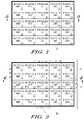
- FIG. 1Illustrated in FIG. 1 is a major surface of a processor die 9 having a plurality of individual and separate processing units 11 - 35 provided in an array having rows and columns. In other forms the processing units 11 - 35 may be placed in an array of geometric configurations other than rows and columns of processing units.
- Each of the processing units 11 - 35is any type of a variety of data processors.
- each of the processing units 11 - 35may be a central processing unit (CPUs), a digital signal processor, a graphics-specific processor, a microcontroller unit (MCU), a communications processor or any other type of processing unit.
- the processing units 11 - 35may be the same type of processing unit or may vary between types of processing unit across the processor die 9 .
- each processing unit rowthere are five rows with each processing unit row having five columns. It should be understood that the illustrated embodiment is exemplary only and any number of X rows and Y columns of processing units may be implemented, where X and Y are integers of two or greater. In one form only four processing units are implemented. Additionally, it should be understood that the physical size or layout area of the processing units 11 - 35 does not necessarily need to be uniform as illustrated in FIG. 1 . When functionally differing types of processing units are implemented, the circuit area consumed by each processing unit may differ. Further it should be understood that while rectangular shapes are provided for each of the processing units 11 - 35 , other geometric shapes may be implemented. In the illustrated form it should be understood that there is provided some physical separation and interconnect between each of the processing units 11 - 35 . However, the amount of die area required to provide this isolation is a limited amount of the total die and is therefore not illustrated. Additionally, it should be noted that substantially all of the area of processor die 9 is dedicated area for the processing units 11 - 35 and this embodiment is therefore very size efficient.
- FIG. 2Illustrated in FIG. 2 is another embodiment wherein a major surface of a processor die 10 has both the processing units 11 - 35 and an external connection region 38 that is peripheral to the processing units 11 - 35 .
- Each of the processing units 11 - 35 that have an external edgeare adjoined by the external connection region 38 . That would therefore be processing units 11 - 15 , 16 , 20 , 21 , 25 , 26 , 30 and 31 - 35 .
- Within the external connection region 38are a plurality of external contact pads 44 that are placed at predetermined locations for providing connections from external the processing units 11 - 35 .
- processing units 21 - 25are also respectively labeled P 1 through P 5 .
- an external contact pad 40is a rectangular-shaped pad for a wire bond connection to circuitry external to the processor die 10 .
- an external contact pad 42is a circular-shaped pad for placement of a conductive bump such as a solder bump.
- the external connection region 38is an area of the die 10 where electrical connection from external to die 10 is made. Underlying the contact pads within the external connection region 38 are conductive routing (not visible from the view of FIG. 2 ) that connects the contact pads to predetermined circuitry within the die 10 .
- the contact padscommunicate power, data, control signals and address signals and provide a way to obtain external access to the processor die 10 .
- FIG. 3Illustrated in FIG. 3 is a top view of a cache die 45 having a plurality or an array of cache units.
- Each of the cache units 46 - 70is a semiconductor cache (i.e. memory).
- Each of the cache units 46 - 70is any type of cache memory.
- each of the processing units 46 - 70may be static random access memory (SRAM), FLASH memory, magnetoresistive random access memory (MRAM), dynamic random access memory (DRAM) or any other type of memory.
- the cache units 46 - 70may be the same type of memory unit or may vary. In the illustrated form there are five rows with each cache unit row having five columns. It should be noted that the illustrated embodiment has the same number of rows and columns of cache units as processing units so that each processing unit is correlated to an exclusive and separate cache unit.
- each cache unit of processor die 9 or processor die 10is for connection to a specific designated one of the cache units of cache die 45 .
- each processing unit in a first diehas a dedicated cache unit in a second die.
- the circuit area consumed by each cache unitmay therefore differ.
- rectangular shapesare provided for each of the cache units 46 - 70 , other geometric shapes may be implemented. In the illustrated form it should be understood that there may be provided some physical separation and interconnect between each of the cache units 46 - 70 .
- the amount of die area required to provide this isolationis a limited amount of the total die and is therefore not illustrated. Additionally, it should be noted that substantially all of the area of processor die 9 is dedicated area for the cache units 46 - 70 and this embodiment is therefore also very size efficient. In the FIG. 3 illustration, the various interconnects to each cache unit are not shown in the top view shown.
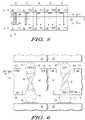
- FIG. 4a cross-section of the processor die 10 and the cache die 45 taken along line 4 - 4 of each of FIG. 2 and FIG. 3 , respectively.
- the connection of processor die 10 and cache die 45 as illustrated in FIG. 4forms a multiple processor/cache assembly wherein the processor die 9 is directly connected to the cache die 45 .
- the processor die 10aligns in a predetermined alignment with the cache die 45 to form regions designated as processor/cache 73 , processor/cache 74 , processor/cache 75 , processor/cache 76 and processor/cache 77 . Within each of these regions, a processor is coterminous with a corresponding cache.
- Cache unit 56is connected to the processing unit 21 via a data bus 80 , an address bus 82 , a control bus 84 and a status bus 86 .
- the data bus 80is bidirectional.
- the address bus 82is unidirectional with the processing unit 21 providing memory addresses directly to the cache unit 56 .
- the control bus 84is also unidirectional wherein the processing unit 21 provides control information to the cache unit 56 to control memory accesses to the cache unit 56 .
- control bus 84may be bidirectional.
- status bus 86is also unidirectional wherein the cache unit 56 provides status information to the processing unit 21 .
- the buses which are discussed hereinmay be physically implemented with any of a variety of physical structures.
- conductive bumpssuch as solder bumps, may be used to form the processor unit/cache unit connections when the processor die 10 is directly attached to the cache die 45 .
- conductive contact padsmay be used on the surface of each of processor die 10 and cache die 45 so that when they are connected together a processing unit is directly connected to a cache unit.
- the contactsare therefore direct and vertical in direction. In this form the direct contacts are short and therefore approximate the electrical properties of a multiple layer single die. Therefore, capacitance and inductance associated with the connectors between a processor and a cache are minimized which improves performance parameters including speed, area and power.
- the processor die 10extends wider than the cache die 45 to expose the external connection region 38 .
- the external contact pad 40is provided for future contact to the multiple processor/cache assembly. Contact to the external contact pad 40 may be made by conductive bump, wire bond or other interconnect methods.
- FIG. 5Illustrated in FIG. 5 is another embodiment wherein an interposer 90 is provided for separating the processor die 9 from the cache die 45 to form a multiple processor/cache assembly 88 .
- the processor die 9 and the cache die 45are implemented with substantially the same width.
- External contact to the multiple processor/cache assembly 88is made by extending the interposer 90 on at least one side beyond the widths of the processor die 9 and the cache die 45 .
- interposer 90is extended to the right.
- An external contact 92 and an external contact 94are positioned on opposing sides of the exposed portion of interposer 90 .
- interposer 90Electrical contact to the exposed contacts of the interposer 90 may be made by various methods such as connecting the interposer 90 in a clip contact which fits around the contacts on both sides of interposer 90 . Alternatively a socket with a recess could be used. In yet another form, the interposer 90 may be fitted into a contact hole in a substrate. In other forms wire bonds or solder ball connections may be made to the external contacts of the interposer 90 .
- the interposer 90may be formed of any of various materials. In one form interposer 90 is silicon. Other suitable materials include heat conducting ceramic or flexible organic film.
- the interposer 90has a plurality of vias or openings for placement of conductive material to implement the conductors of the buses, such as data bus 80 , address bus 82 , control bus 84 and status bus 86 .
- the cache unit 60 or C 5is directly connected to the processing unit 25 or P 5 .
- unit C 4is connected directly to unit P 4 .
- Unit C 3is connected directly to unit P 3
- unit C 2is connected directly to unit P 2 .
- the unit C 1is connected directly to unit P 1 .
- FIG. 6Illustrated in FIG. 6 is a detail of a portion of the processor/cache 74 of FIG. 5 . Connection from the cache die 45 to the processor die 9 via the interposer 90 that is positioned between the two die is illustrated in detail.
- the cache unit 57overlies and connects to the processing unit 22 in FIG. 6 . Only a small portion of each of the cache unit 57 and the processing unit 22 is shown as designated by a break between two portions of the processor/cache 74 .
- An address conductoris illustrated on the left and a data conductor is illustrated on the right.
- the address conductoruses an opening or via in the interposer 90 identified as conductive via 96 .
- conductive via 96is filled with a conductive material such as metal or other electrical conductors.
- a conductive bump 98overlies the conductive via 96 and makes contact to the cache unit 57 by contacting a contact pad 102 .
- a conductive bump 99underlies the conductive via 96 and makes contact to the processing unit 22 via a contact pad 103 .
- Attached to the interposer 90are various conductive traces for carrying power supply signals and other signals such as data.
- the data conductoris implemented by an opening or via in the interposer 90 that is identified as conductive via 97 . Any conductive material may be used to implement the conductive vias.
- a conductive bump 100overlies the conductive via 97 and makes contact to the cache unit 57 by contacting a contact pad 104 .
- a data trace 114 for external connectionunderlies the conductive via 97 and makes contact to the processing unit 22 via a conductive bump 101 at a contact pad 105 .
- an air gapmay exist between the interposer 90 and each of the cache die 45 and the processor die 9 adjacent the conductive bump connections. In other forms the two die may be sufficiently compressed together so that the air gap is very small. In another embodiment a fill material (not shown) may be used to fill the air gap.
- a very direct and short electrical paththerefore exists between a processing unit on a first die and a correlated dedicated cache for that processing unit on a second die that is either above or below the first die.
- the structures provided hereinimplement a multi-processor array that has a specific, dedicated cache memory for each processor efficiently connected.
- the direct contact between a cache memory and a correlated processorpermits customization of the cache regarding type, size, speed, etc. rather than having a common cache memory for multiple processors that likely operate with differing parameters.
- the appropriate matching of cache memory speed with an associated processorpermits efficient customization of a processing system.
- one or more of the cache memories on the cache die 45may be implemented as a dual port cache memory and have first and second input ports respectively connected to two different processing units on processor die 10 .
- the conductive bumps 98 - 101may be initially formed on the interposer 90 rather than on the processor die 10 and the cache die 45 . The placement of the conductive bumps initially on the interposer 90 avoids potential yield issues associated with bumping the die. Any defect associated with the bumping process of a die is much more expensive than with the bumping of an interposer.
- busis used to refer to a plurality of signals or conductors which may be used to transfer one or more various types of information, such as data, addresses, control, or status.
- the conductors as discussed hereinmay be illustrated or described in reference to being a single conductor, a plurality of conductors, unidirectional conductors, or bidirectional conductors. However, different embodiments may vary the implementation of the conductors. For example, separate unidirectional conductors may be used rather than bidirectional conductors and vice versa.
- plurality of conductorsmay be replaced with a single conductor that transfers multiple signals serially or in a time multiplexed manner. Likewise, single conductors carrying multiple signals may be separated out into various different conductors carrying subsets of these signals. Therefore, many options exist for transferring signals.
- a processor/cache assemblyhaving a first semiconductor die having an array of processing units.
- Each processing unit of the array of processing unitshas a set of processor contact pads.
- the processor contact padsare conductive pads on a surface of the first semiconductor die.
- Each set of processor contact padsis unique from the set of processor contact pads of all of the other processing units of the array of processing units.
- Each set of the processor contact padsincludes a first subset of processor contact pads for address signals and a second subset of processor contact pads for data signals.
- a second semiconductor diehas an array of cache units.
- Each cache unit of the array of cache unitshas a set of cache contact pads.
- the cache contact padsare conductive pads on a surface external of the second semiconductor die.
- Each set of cache contact padsis unique from the set of cache contact pads of all of the other cache units of the array of cache units.
- Each set of the external contact padsincludes a first subset of cache contact pads for address signals and a second subset of cache contact pads for data signals.
- the first subset of cache contact pads of each cache unitis connected to the first subset of processor contact pads of a unique one of the processor units.
- the second subset of cache contact pads of each cache unitis connected to the second subset of processor contact pads of the processor unit to which its first subset of cache contact pads is connected.
- the first semiconductor diehas a major surface and the processor contact pads are on the major surface of the first semiconductor die.
- the second semiconductorhas a major surface and the cache contact pads are on the major surface of the second semiconductor die.
- the major surface of the first semiconductor diefaces the major surface of the second semiconductor die.
- the processor contact padsare directly connected to the cache contact pads through conductive bumps.
- the first semiconductor diehas a greater surface area than the second semiconductor die.
- the first semiconductor diehas external contact pads along a periphery of the first semiconductor die for making external connections from the first semiconductor die.
- an interposeris between the major surfaces for connecting the processor contact pads to the cache contact pads.
- the interposerhas traces for carrying power to at least one of a group consisting of the first semiconductor die and the second semiconductor die.
- the interposerextends beyond an outer boundary of the first semiconductor die and the second semiconductor die.
- processor unitshave a first area and the cache units have a second area, wherein the first area and the second area are substantially the same.
- outer boundaries of the processor units and the cache unitsare coterminous.
- each of the processing unitsis the same shape and size as the other processing units.
- array of processing unitshas a first geometric shape and the array of cache units has a second geometric shape that is a mirror image of the first geometric shape.
- a processor dieis formed having an array of processor units being in a first arrangement and having a first plurality of contact pads in a second arrangement.
- a cache dieis formed having an array of cache units being in a third arrangement and having a second plurality of contact pads in a fourth arrangement.
- the third arrangementis a mirror image of the first arrangement
- the fourth arrangementis a mirror image of the second arrangement.
- the first dieis contacted to the second die.
- the processor dieis implemented with the first plurality of contact pads having a plurality of processor sets of contact pads wherein each processor set is unique to one of the processor units and has a first subset of contact pads for carrying an address.
- Forming the cache dieis implemented by a second plurality of contact pads having a plurality of cache sets of contact pads wherein each cache set is unique to one of the cache units and has a second subset of contact pads for carrying an address.
- contacting the first die to the second diecauses each of the processor units to be coterminous with a unique one of the cache units.
- the contactingdirectly connects the first plurality of contacts to the second plurality of contacts through a plurality of solder bumps.
- the contactingis implemented by providing an interposer and connecting the first and second die to the interposer.
- a processor/cache assemblyhaving a processor die having first, second, third, and fourth processor units arranged in an array of processor units.
- First, second, third, and fourth sets of processor contact padsare on a first major surface of the processor die, wherein the first, second, third, and fourth sets of processor contact pads are for carrying addresses from the first, second, third, and fourth processor units, respectively.
- a cache diehas first, second, third, and fourth cache units arranged in an array of cache units.
- First, second, third, and fourth sets of cache contact padsare on a first major surface of the cache die, wherein the first, second, third, and fourth sets of cache contact pads are for receiving addresses from the first, second, third, and fourth processor units, respectively, for the use of the first, second, third, and fourth cache units, respectively.
- fifth, sixth, seventh, and eighth sets of processor contact padsare on the first major surface of the processor die, wherein the fifth, sixth, seventh, and eighth sets of processor contact pads are for carrying data to and from the first, second, third, and fourth processor units, respectively.
- Fifth, sixth, seventh, and eighth sets of cache contact padsare on the first major surface of the cache die, wherein the fifth, sixth, seventh, and eighth sets of cache contact pads are for carrying data to and from the first, second, third, and fourth cache units, respectively.
- first, second, third, and fourth cache unitsare caches dedicated to use by the first, second, third, and fourth processor units, respectively.
- Some of the above embodimentsmay be implemented using a variety of different information processing systems. For example, some systems that implement the disclosed structures may place the processing die in between two memory die wherein separate memory die are both on top and below the processing die. As multiple core systems proliferate any number of processing units may be implemented on a single die. Similarly, a single processing unit may have multiple sub-units of processing units.
- the description of the architecturehas been simplified for purposes of discussion, and it is just one of many different types of appropriate architectures that may be used in accordance with the invention. Those skilled in the art will recognize that the boundaries between logic blocks are merely illustrative and that alternative embodiments may merge logic blocks or circuit elements or impose an alternate decomposition of functionality upon various logic blocks or circuit elements.
- any two components herein combined to achieve a particular functionalitycan be seen as “associated with” each other such that the desired functionality is achieved, irrespective of architectures or intermedial components.
- any two components so associatedcan also be viewed as being “operably connected,” or “operably coupled,” to each other to achieve the desired functionality.
- the multiple processor/memory cache systems described hereinare computer systems such as a personal computer system. Other embodiments may include different types of computer systems.
- Computer systemsare information handling systems which can be designed to give independent computing power to one or more users. Computer systems may be found in many forms including but not limited to mainframes, minicomputers, servers, workstations, personal computers, notepads, personal digital assistants, electronic games, automotive and other embedded systems, cell phones and various other wireless devices.
- a typical computer systemincludes at least one processing unit, associated memory and a number of input/output (I/O) devices.
- a computer systemprocesses information according to a program and produces resultant output information via I/O devices.
- a programis a list of instructions such as a particular application program and/or an operating system.
- a computer programis typically stored internally on computer readable storage medium or transmitted to the computer system via a computer readable transmission medium.
- a computer processtypically includes an executing (running) program or portion of a program, current program values and state information, and the resources used by the operating system to manage the execution of the process.
- a parent processmay spawn other, child processes to help perform the overall functionality of the parent process. Because the parent process specifically spawns the child processes to perform a portion of the overall functionality of the parent process, the functions performed by child processes (and grandchild processes, etc.) may sometimes be described as being performed by the parent process.
- Coupledis not intended to be limited to a direct coupling or a mechanical coupling.
Landscapes
- Engineering & Computer Science (AREA)
- Microelectronics & Electronic Packaging (AREA)
- Power Engineering (AREA)
- Physics & Mathematics (AREA)
- Condensed Matter Physics & Semiconductors (AREA)
- General Physics & Mathematics (AREA)
- Computer Hardware Design (AREA)
- Manufacturing & Machinery (AREA)
- Memory System Of A Hierarchy Structure (AREA)
Abstract
Description
- 1. Field
- This disclosure relates generally to semiconductors, and more specifically, to processing operating speeds that exist in semiconductor packages having multiple die.
- 2. Related Art
- It is well known to stack two or more semiconductor packages on top of each other to reduce footprint area. Others have also proposed stacking two or more semiconductor die on top of each other. Various solutions have been proposed for addressing problems associated with additional heat that is generated when two separate semiconductors are placed in close proximity with each other. The size of the semiconductors and their functions continue to limit the practical use of stacked semiconductors, as well as the ability to efficiently make electrical connections to multiple semiconductors in close proximity.
- Commercial data processing systems typically utilize multiple cores or processing units. For example, it is common in the desktop processing environment for dual core processors to be efficiently used by splitting functions in a method that concurrently processes information. In U.S. Pat. No. 7,279,795 issued to Periaman et al. a stacked die semiconductor is disclosed in which one die is a multiple core processor die and a second die contains a shared memory for the multiple cores. The shared memory must therefore be made large to minimize the number of memory accesses to a main off-chip memory. The effective data communication bandwidth of such a configuration is lowered as compared to a single chip implementation in which each processor core has a memory and a memory control located on the same die. Efficiently addressing both the data communication bandwidth and the size or package footprint issues in multiple processing core systems remains problematic.
- The present invention is illustrated by way of example and is not limited by the accompanying figures, in which like references indicate similar elements. Elements in the figures are illustrated for simplicity and clarity and have not necessarily been drawn to scale.
FIG. 1 illustrates in diagrammatic form a first semiconductor die having a plurality of separate processing units in accordance with a first embodiment;FIG. 2 illustrates in diagrammatic form the first semiconductor die having a plurality of separate processing units in accordance with a second embodiment;FIG. 3 illustrates in diagrammatic form a second semiconductor die having a plurality of semiconductor cache units, each correlated to a specific processing unit of the first semiconductor die;FIG. 4 illustrates in cross-sectional form the physical attributes of the first semiconductor die ofFIG. 2 when joined with the second semiconductor die ofFIG. 3 via associated functional connections;FIG. 5 illustrates in cross-sectional form the physical attributes of the first semiconductor die ofFIG. 1 when joined with the second semiconductor die ofFIG. 3 via an interposer and associated functional connections;FIG. 6 illustrates in cross-sectional form the physical attributes of interposer ofFIG. 5 when connecting a portion of the first semiconductor die to the second semiconductor die.- Illustrated in
FIG. 1 is a major surface of a processor die9 having a plurality of individual and separate processing units11-35 provided in an array having rows and columns. In other forms the processing units11-35 may be placed in an array of geometric configurations other than rows and columns of processing units. Each of the processing units11-35 is any type of a variety of data processors. For example, each of the processing units11-35 may be a central processing unit (CPUs), a digital signal processor, a graphics-specific processor, a microcontroller unit (MCU), a communications processor or any other type of processing unit. Further, the processing units11-35 may be the same type of processing unit or may vary between types of processing unit across the processor die9. In the illustrated form there are five rows with each processing unit row having five columns. It should be understood that the illustrated embodiment is exemplary only and any number of X rows and Y columns of processing units may be implemented, where X and Y are integers of two or greater. In one form only four processing units are implemented. Additionally, it should be understood that the physical size or layout area of the processing units11-35 does not necessarily need to be uniform as illustrated inFIG. 1 . When functionally differing types of processing units are implemented, the circuit area consumed by each processing unit may differ. Further it should be understood that while rectangular shapes are provided for each of the processing units11-35, other geometric shapes may be implemented. In the illustrated form it should be understood that there is provided some physical separation and interconnect between each of the processing units11-35. However, the amount of die area required to provide this isolation is a limited amount of the total die and is therefore not illustrated. Additionally, it should be noted that substantially all of the area of processor die9 is dedicated area for the processing units11-35 and this embodiment is therefore very size efficient. - Illustrated in
FIG. 2 is another embodiment wherein a major surface of a processor die10 has both the processing units11-35 and anexternal connection region 38 that is peripheral to the processing units11-35. Each of the processing units11-35 that have an external edge are adjoined by theexternal connection region 38. That would therefore be processing units11-15,16,20,21,25,26,30 and31-35. Within theexternal connection region 38 are a plurality ofexternal contact pads 44 that are placed at predetermined locations for providing connections from external the processing units11-35. For further reference, processing units21-25 are also respectively labeled P1 through P5. In one form anexternal contact pad 40 is a rectangular-shaped pad for a wire bond connection to circuitry external to the processor die10. Similarly, anexternal contact pad 42 is a circular-shaped pad for placement of a conductive bump such as a solder bump. In this embodiment theexternal connection region 38 is an area of the die10 where electrical connection from external to die10 is made. Underlying the contact pads within theexternal connection region 38 are conductive routing (not visible from the view ofFIG. 2 ) that connects the contact pads to predetermined circuitry within the die10. The contact pads communicate power, data, control signals and address signals and provide a way to obtain external access to the processor die10. - Illustrated in
FIG. 3 is a top view of a cache die45 having a plurality or an array of cache units. Each of the cache units46-70 is a semiconductor cache (i.e. memory). Each of the cache units46-70 is any type of cache memory. For example, each of the processing units46-70 may be static random access memory (SRAM), FLASH memory, magnetoresistive random access memory (MRAM), dynamic random access memory (DRAM) or any other type of memory. The cache units46-70 may be the same type of memory unit or may vary. In the illustrated form there are five rows with each cache unit row having five columns. It should be noted that the illustrated embodiment has the same number of rows and columns of cache units as processing units so that each processing unit is correlated to an exclusive and separate cache unit. - Additionally, it should be understood that the physical size or layout area of the cache units46-70 is intentionally correlated to a predetermined different processing unit of processor die9 of
FIG. 1 or processor die10 ofFIG. 2 . In this correlation, each cache unit of processor die9 or processor die10 is for connection to a specific designated one of the cache units ofcache die 45. As a result, each processing unit in a first die has a dedicated cache unit in a second die. The circuit area consumed by each cache unit may therefore differ. Further it should be understood that while rectangular shapes are provided for each of the cache units46-70, other geometric shapes may be implemented. In the illustrated form it should be understood that there may be provided some physical separation and interconnect between each of the cache units46-70. However, the amount of die area required to provide this isolation is a limited amount of the total die and is therefore not illustrated. Additionally, it should be noted that substantially all of the area of processor die9 is dedicated area for the cache units46-70 and this embodiment is therefore also very size efficient. In theFIG. 3 illustration, the various interconnects to each cache unit are not shown in the top view shown. - To further understand the connections associated with each of the cache units of
FIG. 3 , there is illustrated inFIG. 4 a cross-section of the processor die10 and the cache die45 taken along line4-4 of each ofFIG. 2 andFIG. 3 , respectively. The connection of processor die10 and cache die45 as illustrated inFIG. 4 forms a multiple processor/cache assembly wherein the processor die9 is directly connected to the cache die45. In the illustrated form the processor die10 aligns in a predetermined alignment with the cache die45 to form regions designated as processor/cache 73, processor/cache 74, processor/cache 75, processor/cache 76 and processor/cache 77. Within each of these regions, a processor is coterminous with a corresponding cache. Each region is coterminous or coextensive meaning that they have substantially the same or coincident boundaries. Each of these processor/cache combinations are connected by four multiple-conductor buses as illustrated inFIG. 4 . The number of buses that are used is application dependent and other forms may use less or more buses than illustrated.Cache unit 56 is connected to theprocessing unit 21 via adata bus 80, an address bus82, acontrol bus 84 and astatus bus 86. Thedata bus 80 is bidirectional. The address bus82 is unidirectional with theprocessing unit 21 providing memory addresses directly to thecache unit 56. Thecontrol bus 84 is also unidirectional wherein theprocessing unit 21 provides control information to thecache unit 56 to control memory accesses to thecache unit 56. In some forms thecontrol bus 84 may be bidirectional. Thestatus bus 86 is also unidirectional wherein thecache unit 56 provides status information to theprocessing unit 21. The buses which are discussed herein may be physically implemented with any of a variety of physical structures. In one form conductive bumps, such as solder bumps, may be used to form the processor unit/cache unit connections when the processor die10 is directly attached to the cache die45. In other forms conductive contact pads may be used on the surface of each of processor die10 and cache die45 so that when they are connected together a processing unit is directly connected to a cache unit. The contacts are therefore direct and vertical in direction. In this form the direct contacts are short and therefore approximate the electrical properties of a multiple layer single die. Therefore, capacitance and inductance associated with the connectors between a processor and a cache are minimized which improves performance parameters including speed, area and power. - In the illustrated form of the multiple processor/
cache assembly 72, the processor die10 extends wider than the cache die45 to expose theexternal connection region 38. As illustrated inFIG. 4 , theexternal contact pad 40 is provided for future contact to the multiple processor/cache assembly. Contact to theexternal contact pad 40 may be made by conductive bump, wire bond or other interconnect methods. - Illustrated in
FIG. 5 is another embodiment wherein aninterposer 90 is provided for separating the processor die9 from the cache die45 to form a multiple processor/cache assembly 88. In this form the processor die9 and the cache die45 are implemented with substantially the same width. External contact to the multiple processor/cache assembly 88 is made by extending theinterposer 90 on at least one side beyond the widths of the processor die9 and the cache die45. InFIG. 5 interposer 90 is extended to the right. Anexternal contact 92 and anexternal contact 94 are positioned on opposing sides of the exposed portion ofinterposer 90. Electrical contact to the exposed contacts of theinterposer 90 may be made by various methods such as connecting theinterposer 90 in a clip contact which fits around the contacts on both sides ofinterposer 90. Alternatively a socket with a recess could be used. In yet another form, theinterposer 90 may be fitted into a contact hole in a substrate. In other forms wire bonds or solder ball connections may be made to the external contacts of theinterposer 90. Theinterposer 90 may be formed of any of various materials. In oneform interposer 90 is silicon. Other suitable materials include heat conducting ceramic or flexible organic film. Theinterposer 90 has a plurality of vias or openings for placement of conductive material to implement the conductors of the buses, such asdata bus 80, address bus82,control bus 84 andstatus bus 86. As a result of the physical layout of the cache die45 relative to the processor die9, thecache unit 60 or C5 is directly connected to theprocessing unit 25 or P5. Similarly, unit C4 is connected directly to unit P4. Unit C3 is connected directly to unit P3, and unit C2 is connected directly to unit P2. The unit C1 is connected directly to unit P1. - It should be understood that effective heat sinking techniques may be used in connection with the multiple processor/
cache assembly 88 ofFIGS. 4 and 5 . For example, on the exposed sides or surfaces of the processor die9 and10 and the cache die45, various heat removing structures and materials may be placed. Additionally, depending upon the material used for theinterposer 90 some heat transfer away from the multiple processing cores and caches may be obtained. - Illustrated in
FIG. 6 is a detail of a portion of the processor/cache 74 ofFIG. 5 . Connection from the cache die45 to the processor die9 via theinterposer 90 that is positioned between the two die is illustrated in detail. Thecache unit 57 overlies and connects to theprocessing unit 22 inFIG. 6 . Only a small portion of each of thecache unit 57 and theprocessing unit 22 is shown as designated by a break between two portions of the processor/cache 74. An address conductor is illustrated on the left and a data conductor is illustrated on the right. The address conductor uses an opening or via in theinterposer 90 identified as conductive via96. It should be understood that the opening of conductive via96 is filled with a conductive material such as metal or other electrical conductors. Aconductive bump 98 overlies the conductive via96 and makes contact to thecache unit 57 by contacting acontact pad 102. Aconductive bump 99 underlies the conductive via96 and makes contact to theprocessing unit 22 via acontact pad 103. Attached to theinterposer 90 are various conductive traces for carrying power supply signals and other signals such as data. The data conductor is implemented by an opening or via in theinterposer 90 that is identified as conductive via97. Any conductive material may be used to implement the conductive vias. Aconductive bump 100 overlies the conductive via97 and makes contact to thecache unit 57 by contacting acontact pad 104. Adata trace 114 for external connection underlies the conductive via97 and makes contact to theprocessing unit 22 via aconductive bump 101 at acontact pad 105. It should be understood and noted that an air gap may exist between theinterposer 90 and each of the cache die45 and the processor die9 adjacent the conductive bump connections. In other forms the two die may be sufficiently compressed together so that the air gap is very small. In another embodiment a fill material (not shown) may be used to fill the air gap. In the illustrated form a very direct and short electrical path therefore exists between a processing unit on a first die and a correlated dedicated cache for that processing unit on a second die that is either above or below the first die. The structures provided herein implement a multi-processor array that has a specific, dedicated cache memory for each processor efficiently connected. The direct contact between a cache memory and a correlated processor permits customization of the cache regarding type, size, speed, etc. rather than having a common cache memory for multiple processors that likely operate with differing parameters. The appropriate matching of cache memory speed with an associated processor permits efficient customization of a processing system. It should be further understood that in another implementation one or more of the cache memories on the cache die45 may be implemented as a dual port cache memory and have first and second input ports respectively connected to two different processing units on processor die10. It should also be noted that the conductive bumps98-101 may be initially formed on theinterposer 90 rather than on the processor die10 and the cache die45. The placement of the conductive bumps initially on theinterposer 90 avoids potential yield issues associated with bumping the die. Any defect associated with the bumping process of a die is much more expensive than with the bumping of an interposer. - As used herein, the term “bus” is used to refer to a plurality of signals or conductors which may be used to transfer one or more various types of information, such as data, addresses, control, or status. The conductors as discussed herein may be illustrated or described in reference to being a single conductor, a plurality of conductors, unidirectional conductors, or bidirectional conductors. However, different embodiments may vary the implementation of the conductors. For example, separate unidirectional conductors may be used rather than bidirectional conductors and vice versa. Also, plurality of conductors may be replaced with a single conductor that transfers multiple signals serially or in a time multiplexed manner. Likewise, single conductors carrying multiple signals may be separated out into various different conductors carrying subsets of these signals. Therefore, many options exist for transferring signals.
- By now it should be appreciated that there has been provided a high bandwidth communication system between a multiple processor (multi-core) array and a cache memory. Using vertical connections with an interposer between a physically matched cache memory provides efficient area use and high bandwidth due to the short and direct connections. Each processor or core in an array within a die has an overlayed cache memory that is physically aligned to directly connect in a stacked die combination. The various embodiments described herein implement a pair of matched semiconductor die with a one-to-one alignment of each correlated processor/cache memory pair. As a result, very large cache memories may be implemented physically adjacent or next to a processor core without increasing the die size of the processor. By implementing large storage cache memories, the requirement to use an external main system memory is reduced and the system efficiency is dramatically improved. Lower bandwidth requirements to the main memory therefore result.
- In one form there is herein provided a processor/cache assembly having a first semiconductor die having an array of processing units. Each processing unit of the array of processing units has a set of processor contact pads. The processor contact pads are conductive pads on a surface of the first semiconductor die. Each set of processor contact pads is unique from the set of processor contact pads of all of the other processing units of the array of processing units. Each set of the processor contact pads includes a first subset of processor contact pads for address signals and a second subset of processor contact pads for data signals. A second semiconductor die has an array of cache units. Each cache unit of the array of cache units has a set of cache contact pads. The cache contact pads are conductive pads on a surface external of the second semiconductor die. Each set of cache contact pads is unique from the set of cache contact pads of all of the other cache units of the array of cache units. Each set of the external contact pads includes a first subset of cache contact pads for address signals and a second subset of cache contact pads for data signals. The first subset of cache contact pads of each cache unit is connected to the first subset of processor contact pads of a unique one of the processor units. The second subset of cache contact pads of each cache unit is connected to the second subset of processor contact pads of the processor unit to which its first subset of cache contact pads is connected. In one form the first semiconductor die has a major surface and the processor contact pads are on the major surface of the first semiconductor die. The second semiconductor has a major surface and the cache contact pads are on the major surface of the second semiconductor die. The major surface of the first semiconductor die faces the major surface of the second semiconductor die. In another form the processor contact pads are directly connected to the cache contact pads through conductive bumps. In yet another form the first semiconductor die has a greater surface area than the second semiconductor die. In yet another form the first semiconductor die has external contact pads along a periphery of the first semiconductor die for making external connections from the first semiconductor die. In another form an interposer is between the major surfaces for connecting the processor contact pads to the cache contact pads. In yet another form the interposer has traces for carrying power to at least one of a group consisting of the first semiconductor die and the second semiconductor die. In another form the interposer extends beyond an outer boundary of the first semiconductor die and the second semiconductor die. In another form the processor units have a first area and the cache units have a second area, wherein the first area and the second area are substantially the same. In yet another form the outer boundaries of the processor units and the cache units are coterminous. In another form each of the processing units is the same shape and size as the other processing units. In another form the array of processing units has a first geometric shape and the array of cache units has a second geometric shape that is a mirror image of the first geometric shape.
- In yet another form there is provided a method of making a processor/cache assembly. A processor die is formed having an array of processor units being in a first arrangement and having a first plurality of contact pads in a second arrangement. A cache die is formed having an array of cache units being in a third arrangement and having a second plurality of contact pads in a fourth arrangement. The third arrangement is a mirror image of the first arrangement, and the fourth arrangement is a mirror image of the second arrangement. The first die is contacted to the second die. In one form forming the processor die is implemented with the first plurality of contact pads having a plurality of processor sets of contact pads wherein each processor set is unique to one of the processor units and has a first subset of contact pads for carrying an address. Forming the cache die is implemented by a second plurality of contact pads having a plurality of cache sets of contact pads wherein each cache set is unique to one of the cache units and has a second subset of contact pads for carrying an address. In another form contacting the first die to the second die causes each of the processor units to be coterminous with a unique one of the cache units. In another form the contacting directly connects the first plurality of contacts to the second plurality of contacts through a plurality of solder bumps. In another form the contacting is implemented by providing an interposer and connecting the first and second die to the interposer.
- In another form there is provided a processor/cache assembly having a processor die having first, second, third, and fourth processor units arranged in an array of processor units. First, second, third, and fourth sets of processor contact pads are on a first major surface of the processor die, wherein the first, second, third, and fourth sets of processor contact pads are for carrying addresses from the first, second, third, and fourth processor units, respectively. A cache die has first, second, third, and fourth cache units arranged in an array of cache units. First, second, third, and fourth sets of cache contact pads are on a first major surface of the cache die, wherein the first, second, third, and fourth sets of cache contact pads are for receiving addresses from the first, second, third, and fourth processor units, respectively, for the use of the first, second, third, and fourth cache units, respectively. In another form fifth, sixth, seventh, and eighth sets of processor contact pads are on the first major surface of the processor die, wherein the fifth, sixth, seventh, and eighth sets of processor contact pads are for carrying data to and from the first, second, third, and fourth processor units, respectively. Fifth, sixth, seventh, and eighth sets of cache contact pads are on the first major surface of the cache die, wherein the fifth, sixth, seventh, and eighth sets of cache contact pads are for carrying data to and from the first, second, third, and fourth cache units, respectively. In yet another form the first, second, third, and fourth cache units are caches dedicated to use by the first, second, third, and fourth processor units, respectively.
- Because the apparatus implementing the present invention is, for the most part, composed of electronic components and circuits known to those skilled in the art, circuit details will not be explained in any greater extent than that considered necessary as illustrated above, for the understanding and appreciation of the underlying concepts of the present invention and in order not to obfuscate or distract from the teachings of the present invention.
- Moreover, the terms “front,” “back,” “top,” “bottom,” “over,” “under” and the like in the description and in the claims, if any, are used for descriptive purposes and not necessarily for describing permanent relative positions. It is understood that the terms so used are interchangeable under appropriate circumstances such that the embodiments of the invention described herein are, for example, capable of operation in other orientations than those illustrated or otherwise described herein.
- Some of the above embodiments, as applicable, may be implemented using a variety of different information processing systems. For example, some systems that implement the disclosed structures may place the processing die in between two memory die wherein separate memory die are both on top and below the processing die. As multiple core systems proliferate any number of processing units may be implemented on a single die. Similarly, a single processing unit may have multiple sub-units of processing units. Of course, the description of the architecture has been simplified for purposes of discussion, and it is just one of many different types of appropriate architectures that may be used in accordance with the invention. Those skilled in the art will recognize that the boundaries between logic blocks are merely illustrative and that alternative embodiments may merge logic blocks or circuit elements or impose an alternate decomposition of functionality upon various logic blocks or circuit elements.
- Thus, it is to be understood that the architectures depicted herein are merely exemplary, and that in fact many other architectures can be implemented which achieve the same functionality. In an abstract, but still definite sense, any arrangement of components to achieve the same functionality is effectively “associated” such that the desired functionality is achieved. Hence, any two components herein combined to achieve a particular functionality can be seen as “associated with” each other such that the desired functionality is achieved, irrespective of architectures or intermedial components. Likewise, any two components so associated can also be viewed as being “operably connected,” or “operably coupled,” to each other to achieve the desired functionality.
- Furthermore, those skilled in the art will recognize that boundaries between the functionality of the above described operations merely illustrative. The functionality of multiple operations may be combined into a single operation, and/or the functionality of a single operation may be distributed in additional operations. Moreover, alternative embodiments may include multiple instances of a particular operation, and the order of operations may be altered in various other embodiments.
- In one embodiment, the multiple processor/memory cache systems described herein are computer systems such as a personal computer system. Other embodiments may include different types of computer systems. Computer systems are information handling systems which can be designed to give independent computing power to one or more users. Computer systems may be found in many forms including but not limited to mainframes, minicomputers, servers, workstations, personal computers, notepads, personal digital assistants, electronic games, automotive and other embedded systems, cell phones and various other wireless devices. A typical computer system includes at least one processing unit, associated memory and a number of input/output (I/O) devices.
- A computer system processes information according to a program and produces resultant output information via I/O devices. A program is a list of instructions such as a particular application program and/or an operating system. A computer program is typically stored internally on computer readable storage medium or transmitted to the computer system via a computer readable transmission medium. A computer process typically includes an executing (running) program or portion of a program, current program values and state information, and the resources used by the operating system to manage the execution of the process. A parent process may spawn other, child processes to help perform the overall functionality of the parent process. Because the parent process specifically spawns the child processes to perform a portion of the overall functionality of the parent process, the functions performed by child processes (and grandchild processes, etc.) may sometimes be described as being performed by the parent process.
- Although the invention is described herein with reference to specific embodiments, various modifications and changes can be made without departing from the scope of the present invention as set forth in the claims below. For example, other forms of conductive contacts besides conductive bumps may be used. In one form conductive pads on both the semiconductor die and the interposer may be used. Accordingly, the specification and figures are to be regarded in an illustrative rather than a restrictive sense, and all such modifications are intended to be included within the scope of the present invention. Any benefits, advantages, or solutions to problems that are described herein with regard to specific embodiments are not intended to be construed as a critical, required, or essential feature or element of any or all the claims.
- The term “coupled,” as used herein, is not intended to be limited to a direct coupling or a mechanical coupling.
- Furthermore, the terms “a” or “an,” as used herein, are defined as one or more than one. Also, the use of introductory phrases such as “at least one” and “one or more” in the claims should not be construed to imply that the introduction of another claim element by the indefinite articles “a” or “an” limits any particular claim containing such introduced claim element to inventions containing only one such element, even when the same claim includes the introductory phrases “one or more” or “at least one” and indefinite articles such as “a” or “an.” The same holds true for the use of definite articles.
- Unless stated otherwise, terms such as “first” and “second” are used to arbitrarily distinguish between the elements such terms describe. Thus, these terms are not necessarily intended to indicate temporal or other prioritization of such elements.
Claims (20)
Priority Applications (3)
| Application Number | Priority Date | Filing Date | Title |
|---|---|---|---|
| US12/026,325US7777330B2 (en) | 2008-02-05 | 2008-02-05 | High bandwidth cache-to-processing unit communication in a multiple processor/cache system |
| PCT/US2009/030255WO2009099693A1 (en) | 2008-02-05 | 2009-01-07 | High bandwidth cache-to-processing unit communication in a multiple processor/cache system |
| TW098101922ATWI457764B (en) | 2008-02-05 | 2009-01-19 | Processor/cache assembly |
Applications Claiming Priority (1)
| Application Number | Priority Date | Filing Date | Title |
|---|---|---|---|
| US12/026,325US7777330B2 (en) | 2008-02-05 | 2008-02-05 | High bandwidth cache-to-processing unit communication in a multiple processor/cache system |
Publications (2)
| Publication Number | Publication Date |
|---|---|
| US20090196086A1true US20090196086A1 (en) | 2009-08-06 |
| US7777330B2 US7777330B2 (en) | 2010-08-17 |
Family
ID=40931543
Family Applications (1)
| Application Number | Title | Priority Date | Filing Date |
|---|---|---|---|
| US12/026,325Expired - Fee RelatedUS7777330B2 (en) | 2008-02-05 | 2008-02-05 | High bandwidth cache-to-processing unit communication in a multiple processor/cache system |
Country Status (3)
| Country | Link |
|---|---|
| US (1) | US7777330B2 (en) |
| TW (1) | TWI457764B (en) |
| WO (1) | WO2009099693A1 (en) |
Cited By (7)
| Publication number | Priority date | Publication date | Assignee | Title |
|---|---|---|---|---|
| WO2012055780A1 (en)* | 2010-10-28 | 2012-05-03 | International Business Machines Corporation | Optimized semiconductor packaging in a three-dimensional stack |
| US20120105145A1 (en)* | 2010-10-28 | 2012-05-03 | International Business Machines Corporation | Thermal Power Plane for Integrated Circuits |
| US8405998B2 (en) | 2010-10-28 | 2013-03-26 | International Business Machines Corporation | Heat sink integrated power delivery and distribution for integrated circuits |
| US20130159630A1 (en)* | 2011-12-20 | 2013-06-20 | Ati Technologies Ulc | Selective cache for inter-operations in a processor-based environment |
| CN104752387A (en)* | 2013-12-31 | 2015-07-01 | 禾瑞亚科技股份有限公司 | Circuit configuration of touch integrated circuit |
| US20210407966A1 (en)* | 2020-06-29 | 2021-12-30 | Taiwan Semiconductor Manufacturing Company, Ltd. | Semiconductor package |
| WO2025070982A1 (en)* | 2023-09-27 | 2025-04-03 | 삼성전자주식회사 | Integrated circuit including vertical electrical connection connecting plurality of semiconductor dies, and electronic device including same |
Families Citing this family (231)
| Publication number | Priority date | Publication date | Assignee | Title |
|---|---|---|---|---|
| US9509313B2 (en) | 2009-04-14 | 2016-11-29 | Monolithic 3D Inc. | 3D semiconductor device |
| US7986042B2 (en) | 2009-04-14 | 2011-07-26 | Monolithic 3D Inc. | Method for fabrication of a semiconductor device and structure |
| US8395191B2 (en) | 2009-10-12 | 2013-03-12 | Monolithic 3D Inc. | Semiconductor device and structure |
| US8362482B2 (en) | 2009-04-14 | 2013-01-29 | Monolithic 3D Inc. | Semiconductor device and structure |
| US8754533B2 (en) | 2009-04-14 | 2014-06-17 | Monolithic 3D Inc. | Monolithic three-dimensional semiconductor device and structure |
| US8669778B1 (en) | 2009-04-14 | 2014-03-11 | Monolithic 3D Inc. | Method for design and manufacturing of a 3D semiconductor device |
| US8058137B1 (en) | 2009-04-14 | 2011-11-15 | Monolithic 3D Inc. | Method for fabrication of a semiconductor device and structure |
| US8373439B2 (en) | 2009-04-14 | 2013-02-12 | Monolithic 3D Inc. | 3D semiconductor device |
| US8115511B2 (en)* | 2009-04-14 | 2012-02-14 | Monolithic 3D Inc. | Method for fabrication of a semiconductor device and structure |
| US8378715B2 (en) | 2009-04-14 | 2013-02-19 | Monolithic 3D Inc. | Method to construct systems |
| US8258810B2 (en) | 2010-09-30 | 2012-09-04 | Monolithic 3D Inc. | 3D semiconductor device |
| US8384426B2 (en) | 2009-04-14 | 2013-02-26 | Monolithic 3D Inc. | Semiconductor device and structure |
| US8405420B2 (en) | 2009-04-14 | 2013-03-26 | Monolithic 3D Inc. | System comprising a semiconductor device and structure |
| US8362800B2 (en) | 2010-10-13 | 2013-01-29 | Monolithic 3D Inc. | 3D semiconductor device including field repairable logics |
| US9711407B2 (en) | 2009-04-14 | 2017-07-18 | Monolithic 3D Inc. | Method of manufacturing a three dimensional integrated circuit by transfer of a mono-crystalline layer |
| US9577642B2 (en) | 2009-04-14 | 2017-02-21 | Monolithic 3D Inc. | Method to form a 3D semiconductor device |
| US8427200B2 (en) | 2009-04-14 | 2013-04-23 | Monolithic 3D Inc. | 3D semiconductor device |
| US9406561B2 (en)* | 2009-04-20 | 2016-08-02 | International Business Machines Corporation | Three dimensional integrated circuit integration using dielectric bonding first and through via formation last |
| US8581349B1 (en) | 2011-05-02 | 2013-11-12 | Monolithic 3D Inc. | 3D memory semiconductor device and structure |
| US10388863B2 (en) | 2009-10-12 | 2019-08-20 | Monolithic 3D Inc. | 3D memory device and structure |
| US11984445B2 (en) | 2009-10-12 | 2024-05-14 | Monolithic 3D Inc. | 3D semiconductor devices and structures with metal layers |
| US8742476B1 (en) | 2012-11-27 | 2014-06-03 | Monolithic 3D Inc. | Semiconductor device and structure |
| US10910364B2 (en) | 2009-10-12 | 2021-02-02 | Monolitaic 3D Inc. | 3D semiconductor device |
| US10354995B2 (en) | 2009-10-12 | 2019-07-16 | Monolithic 3D Inc. | Semiconductor memory device and structure |
| US10043781B2 (en) | 2009-10-12 | 2018-08-07 | Monolithic 3D Inc. | 3D semiconductor device and structure |
| US12027518B1 (en) | 2009-10-12 | 2024-07-02 | Monolithic 3D Inc. | 3D semiconductor devices and structures with metal layers |
| US11374118B2 (en) | 2009-10-12 | 2022-06-28 | Monolithic 3D Inc. | Method to form a 3D integrated circuit |
| US9099424B1 (en) | 2012-08-10 | 2015-08-04 | Monolithic 3D Inc. | Semiconductor system, device and structure with heat removal |
| US8476145B2 (en) | 2010-10-13 | 2013-07-02 | Monolithic 3D Inc. | Method of fabricating a semiconductor device and structure |
| US8450804B2 (en) | 2011-03-06 | 2013-05-28 | Monolithic 3D Inc. | Semiconductor device and structure for heat removal |
| US11018133B2 (en) | 2009-10-12 | 2021-05-25 | Monolithic 3D Inc. | 3D integrated circuit |
| US10157909B2 (en) | 2009-10-12 | 2018-12-18 | Monolithic 3D Inc. | 3D semiconductor device and structure |
| US10366970B2 (en) | 2009-10-12 | 2019-07-30 | Monolithic 3D Inc. | 3D semiconductor device and structure |
| US8536023B2 (en) | 2010-11-22 | 2013-09-17 | Monolithic 3D Inc. | Method of manufacturing a semiconductor device and structure |
| US8148728B2 (en) | 2009-10-12 | 2012-04-03 | Monolithic 3D, Inc. | Method for fabrication of a semiconductor device and structure |
| US8541819B1 (en) | 2010-12-09 | 2013-09-24 | Monolithic 3D Inc. | Semiconductor device and structure |
| US8492886B2 (en) | 2010-02-16 | 2013-07-23 | Monolithic 3D Inc | 3D integrated circuit with logic |
| US8461035B1 (en) | 2010-09-30 | 2013-06-11 | Monolithic 3D Inc. | Method for fabrication of a semiconductor device and structure |
| US8373230B1 (en) | 2010-10-13 | 2013-02-12 | Monolithic 3D Inc. | Method for fabrication of a semiconductor device and structure |
| US8026521B1 (en) | 2010-10-11 | 2011-09-27 | Monolithic 3D Inc. | Semiconductor device and structure |
| US8298875B1 (en) | 2011-03-06 | 2012-10-30 | Monolithic 3D Inc. | Method for fabrication of a semiconductor device and structure |
| US9099526B2 (en) | 2010-02-16 | 2015-08-04 | Monolithic 3D Inc. | Integrated circuit device and structure |
| US9219005B2 (en) | 2011-06-28 | 2015-12-22 | Monolithic 3D Inc. | Semiconductor system and device |
| US10217667B2 (en) | 2011-06-28 | 2019-02-26 | Monolithic 3D Inc. | 3D semiconductor device, fabrication method and system |
| US8901613B2 (en) | 2011-03-06 | 2014-12-02 | Monolithic 3D Inc. | Semiconductor device and structure for heat removal |
| US9953925B2 (en) | 2011-06-28 | 2018-04-24 | Monolithic 3D Inc. | Semiconductor system and device |
| US8642416B2 (en) | 2010-07-30 | 2014-02-04 | Monolithic 3D Inc. | Method of forming three dimensional integrated circuit devices using layer transfer technique |
| US12362219B2 (en) | 2010-11-18 | 2025-07-15 | Monolithic 3D Inc. | 3D semiconductor memory device and structure |
| US10497713B2 (en) | 2010-11-18 | 2019-12-03 | Monolithic 3D Inc. | 3D semiconductor memory device and structure |
| US11482440B2 (en) | 2010-12-16 | 2022-10-25 | Monolithic 3D Inc. | 3D semiconductor device and structure with a built-in test circuit for repairing faulty circuits |
| US8163581B1 (en) | 2010-10-13 | 2012-04-24 | Monolith IC 3D | Semiconductor and optoelectronic devices |
| US8273610B2 (en) | 2010-11-18 | 2012-09-25 | Monolithic 3D Inc. | Method of constructing a semiconductor device and structure |
| US11158674B2 (en) | 2010-10-11 | 2021-10-26 | Monolithic 3D Inc. | Method to produce a 3D semiconductor device and structure |
| US11018191B1 (en) | 2010-10-11 | 2021-05-25 | Monolithic 3D Inc. | 3D semiconductor device and structure |
| US10290682B2 (en) | 2010-10-11 | 2019-05-14 | Monolithic 3D Inc. | 3D IC semiconductor device and structure with stacked memory |
| US11227897B2 (en) | 2010-10-11 | 2022-01-18 | Monolithic 3D Inc. | Method for producing a 3D semiconductor memory device and structure |
| US11257867B1 (en) | 2010-10-11 | 2022-02-22 | Monolithic 3D Inc. | 3D semiconductor device and structure with oxide bonds |
| US11600667B1 (en) | 2010-10-11 | 2023-03-07 | Monolithic 3D Inc. | Method to produce 3D semiconductor devices and structures with memory |
| US11024673B1 (en) | 2010-10-11 | 2021-06-01 | Monolithic 3D Inc. | 3D semiconductor device and structure |
| US11315980B1 (en) | 2010-10-11 | 2022-04-26 | Monolithic 3D Inc. | 3D semiconductor device and structure with transistors |
| US11469271B2 (en) | 2010-10-11 | 2022-10-11 | Monolithic 3D Inc. | Method to produce 3D semiconductor devices and structures with memory |
| US10896931B1 (en) | 2010-10-11 | 2021-01-19 | Monolithic 3D Inc. | 3D semiconductor device and structure |
| US8114757B1 (en) | 2010-10-11 | 2012-02-14 | Monolithic 3D Inc. | Semiconductor device and structure |
| US8379458B1 (en) | 2010-10-13 | 2013-02-19 | Monolithic 3D Inc. | Semiconductor device and structure |
| US11694922B2 (en) | 2010-10-13 | 2023-07-04 | Monolithic 3D Inc. | Multilevel semiconductor device and structure with oxide bonding |
| US11869915B2 (en) | 2010-10-13 | 2024-01-09 | Monolithic 3D Inc. | Multilevel semiconductor device and structure with image sensors and wafer bonding |
| US8283215B2 (en) | 2010-10-13 | 2012-10-09 | Monolithic 3D Inc. | Semiconductor and optoelectronic devices |
| US9197804B1 (en) | 2011-10-14 | 2015-11-24 | Monolithic 3D Inc. | Semiconductor and optoelectronic devices |
| US11855100B2 (en) | 2010-10-13 | 2023-12-26 | Monolithic 3D Inc. | Multilevel semiconductor device and structure with oxide bonding |
| US12094892B2 (en) | 2010-10-13 | 2024-09-17 | Monolithic 3D Inc. | 3D micro display device and structure |
| US12080743B2 (en) | 2010-10-13 | 2024-09-03 | Monolithic 3D Inc. | Multilevel semiconductor device and structure with image sensors and wafer bonding |
| US11327227B2 (en) | 2010-10-13 | 2022-05-10 | Monolithic 3D Inc. | Multilevel semiconductor device and structure with electromagnetic modulators |
| US11437368B2 (en) | 2010-10-13 | 2022-09-06 | Monolithic 3D Inc. | Multilevel semiconductor device and structure with oxide bonding |
| US11404466B2 (en) | 2010-10-13 | 2022-08-02 | Monolithic 3D Inc. | Multilevel semiconductor device and structure with image sensors |
| US11164898B2 (en) | 2010-10-13 | 2021-11-02 | Monolithic 3D Inc. | Multilevel semiconductor device and structure |
| US11855114B2 (en) | 2010-10-13 | 2023-12-26 | Monolithic 3D Inc. | Multilevel semiconductor device and structure with image sensors and wafer bonding |
| US11043523B1 (en) | 2010-10-13 | 2021-06-22 | Monolithic 3D Inc. | Multilevel semiconductor device and structure with image sensors |
| US11984438B2 (en) | 2010-10-13 | 2024-05-14 | Monolithic 3D Inc. | Multilevel semiconductor device and structure with oxide bonding |
| US11133344B2 (en) | 2010-10-13 | 2021-09-28 | Monolithic 3D Inc. | Multilevel semiconductor device and structure with image sensors |
| US12360310B2 (en) | 2010-10-13 | 2025-07-15 | Monolithic 3D Inc. | Multilevel semiconductor device and structure with oxide bonding |
| US11929372B2 (en) | 2010-10-13 | 2024-03-12 | Monolithic 3D Inc. | Multilevel semiconductor device and structure with image sensors and wafer bonding |
| US10679977B2 (en) | 2010-10-13 | 2020-06-09 | Monolithic 3D Inc. | 3D microdisplay device and structure |
| US11063071B1 (en) | 2010-10-13 | 2021-07-13 | Monolithic 3D Inc. | Multilevel semiconductor device and structure with waveguides |
| US11605663B2 (en) | 2010-10-13 | 2023-03-14 | Monolithic 3D Inc. | Multilevel semiconductor device and structure with image sensors and wafer bonding |
| US10943934B2 (en) | 2010-10-13 | 2021-03-09 | Monolithic 3D Inc. | Multilevel semiconductor device and structure |
| US10978501B1 (en) | 2010-10-13 | 2021-04-13 | Monolithic 3D Inc. | Multilevel semiconductor device and structure with waveguides |
| US10833108B2 (en) | 2010-10-13 | 2020-11-10 | Monolithic 3D Inc. | 3D microdisplay device and structure |
| US10998374B1 (en) | 2010-10-13 | 2021-05-04 | Monolithic 3D Inc. | Multilevel semiconductor device and structure |
| US11163112B2 (en) | 2010-10-13 | 2021-11-02 | Monolithic 3D Inc. | Multilevel semiconductor device and structure with electromagnetic modulators |
| US11443971B2 (en) | 2010-11-18 | 2022-09-13 | Monolithic 3D Inc. | 3D semiconductor device and structure with memory |
| US12272586B2 (en) | 2010-11-18 | 2025-04-08 | Monolithic 3D Inc. | 3D semiconductor memory device and structure with memory and metal layers |
| US11615977B2 (en) | 2010-11-18 | 2023-03-28 | Monolithic 3D Inc. | 3D semiconductor memory device and structure |
| US11355380B2 (en) | 2010-11-18 | 2022-06-07 | Monolithic 3D Inc. | Methods for producing 3D semiconductor memory device and structure utilizing alignment marks |
| US11121021B2 (en) | 2010-11-18 | 2021-09-14 | Monolithic 3D Inc. | 3D semiconductor device and structure |
| US11610802B2 (en) | 2010-11-18 | 2023-03-21 | Monolithic 3D Inc. | Method for producing a 3D semiconductor device and structure with single crystal transistors and metal gate electrodes |
| US11004719B1 (en) | 2010-11-18 | 2021-05-11 | Monolithic 3D Inc. | Methods for producing a 3D semiconductor memory device and structure |
| US11784082B2 (en) | 2010-11-18 | 2023-10-10 | Monolithic 3D Inc. | 3D semiconductor device and structure with bonding |
| US12144190B2 (en) | 2010-11-18 | 2024-11-12 | Monolithic 3D Inc. | 3D semiconductor device and structure with bonding and memory cells preliminary class |
| US11107721B2 (en) | 2010-11-18 | 2021-08-31 | Monolithic 3D Inc. | 3D semiconductor device and structure with NAND logic |
| US11495484B2 (en) | 2010-11-18 | 2022-11-08 | Monolithic 3D Inc. | 3D semiconductor devices and structures with at least two single-crystal layers |
| US11482439B2 (en) | 2010-11-18 | 2022-10-25 | Monolithic 3D Inc. | Methods for producing a 3D semiconductor memory device comprising charge trap junction-less transistors |
| US11901210B2 (en) | 2010-11-18 | 2024-02-13 | Monolithic 3D Inc. | 3D semiconductor device and structure with memory |
| US11854857B1 (en) | 2010-11-18 | 2023-12-26 | Monolithic 3D Inc. | Methods for producing a 3D semiconductor device and structure with memory cells and multiple metal layers |
| US11355381B2 (en) | 2010-11-18 | 2022-06-07 | Monolithic 3D Inc. | 3D semiconductor memory device and structure |
| US11482438B2 (en) | 2010-11-18 | 2022-10-25 | Monolithic 3D Inc. | Methods for producing a 3D semiconductor memory device and structure |
| US11735462B2 (en) | 2010-11-18 | 2023-08-22 | Monolithic 3D Inc. | 3D semiconductor device and structure with single-crystal layers |
| US11018042B1 (en) | 2010-11-18 | 2021-05-25 | Monolithic 3D Inc. | 3D semiconductor memory device and structure |
| US11211279B2 (en) | 2010-11-18 | 2021-12-28 | Monolithic 3D Inc. | Method for processing a 3D integrated circuit and structure |
| US11508605B2 (en) | 2010-11-18 | 2022-11-22 | Monolithic 3D Inc. | 3D semiconductor memory device and structure |
| US11094576B1 (en) | 2010-11-18 | 2021-08-17 | Monolithic 3D Inc. | Methods for producing a 3D semiconductor memory device and structure |
| US11521888B2 (en) | 2010-11-18 | 2022-12-06 | Monolithic 3D Inc. | 3D semiconductor device and structure with high-k metal gate transistors |
| US11031275B2 (en) | 2010-11-18 | 2021-06-08 | Monolithic 3D Inc. | 3D semiconductor device and structure with memory |
| US11923230B1 (en) | 2010-11-18 | 2024-03-05 | Monolithic 3D Inc. | 3D semiconductor device and structure with bonding |
| US11804396B2 (en) | 2010-11-18 | 2023-10-31 | Monolithic 3D Inc. | Methods for producing a 3D semiconductor device and structure with memory cells and multiple metal layers |
| US11569117B2 (en) | 2010-11-18 | 2023-01-31 | Monolithic 3D Inc. | 3D semiconductor device and structure with single-crystal layers |
| US12033884B2 (en) | 2010-11-18 | 2024-07-09 | Monolithic 3D Inc. | Methods for producing a 3D semiconductor device and structure with memory cells and multiple metal layers |
| US12125737B1 (en) | 2010-11-18 | 2024-10-22 | Monolithic 3D Inc. | 3D semiconductor device and structure with metal layers and memory cells |
| US12136562B2 (en) | 2010-11-18 | 2024-11-05 | Monolithic 3D Inc. | 3D semiconductor device and structure with single-crystal layers |
| US12068187B2 (en) | 2010-11-18 | 2024-08-20 | Monolithic 3D Inc. | 3D semiconductor device and structure with bonding and DRAM memory cells |
| US11862503B2 (en) | 2010-11-18 | 2024-01-02 | Monolithic 3D Inc. | Method for producing a 3D semiconductor device and structure with memory cells and multiple metal layers |
| US12100611B2 (en) | 2010-11-18 | 2024-09-24 | Monolithic 3D Inc. | Methods for producing a 3D semiconductor device and structure with memory cells and multiple metal layers |
| US12243765B2 (en) | 2010-11-18 | 2025-03-04 | Monolithic 3D Inc. | 3D semiconductor device and structure with metal layers and memory cells |
| US12154817B1 (en) | 2010-11-18 | 2024-11-26 | Monolithic 3D Inc. | Methods for producing a 3D semiconductor memory device and structure |
| US11164770B1 (en) | 2010-11-18 | 2021-11-02 | Monolithic 3D Inc. | Method for producing a 3D semiconductor memory device and structure |
| US8975670B2 (en) | 2011-03-06 | 2015-03-10 | Monolithic 3D Inc. | Semiconductor device and structure for heat removal |
| US10388568B2 (en) | 2011-06-28 | 2019-08-20 | Monolithic 3D Inc. | 3D semiconductor device and system |
| US8687399B2 (en) | 2011-10-02 | 2014-04-01 | Monolithic 3D Inc. | Semiconductor device and structure |
| US20130082365A1 (en) | 2011-10-03 | 2013-04-04 | International Business Machines Corporation | Interposer for ESD, EMI, and EMC |
| US8796822B2 (en) | 2011-10-07 | 2014-08-05 | Freescale Semiconductor, Inc. | Stacked semiconductor devices |
| US9076664B2 (en) | 2011-10-07 | 2015-07-07 | Freescale Semiconductor, Inc. | Stacked semiconductor die with continuous conductive vias |
| US9029173B2 (en) | 2011-10-18 | 2015-05-12 | Monolithic 3D Inc. | Method for fabrication of a semiconductor device and structure |
| US9000557B2 (en) | 2012-03-17 | 2015-04-07 | Zvi Or-Bach | Semiconductor device and structure |
| US11164811B2 (en) | 2012-04-09 | 2021-11-02 | Monolithic 3D Inc. | 3D semiconductor device with isolation layers and oxide-to-oxide bonding |
| US11735501B1 (en) | 2012-04-09 | 2023-08-22 | Monolithic 3D Inc. | 3D semiconductor device and structure with metal layers and a connective path |
| US11410912B2 (en) | 2012-04-09 | 2022-08-09 | Monolithic 3D Inc. | 3D semiconductor device with vias and isolation layers |
| US10600888B2 (en) | 2012-04-09 | 2020-03-24 | Monolithic 3D Inc. | 3D semiconductor device |
| US11088050B2 (en) | 2012-04-09 | 2021-08-10 | Monolithic 3D Inc. | 3D semiconductor device with isolation layers |
| US11616004B1 (en) | 2012-04-09 | 2023-03-28 | Monolithic 3D Inc. | 3D semiconductor device and structure with metal layers and a connective path |
| US8557632B1 (en) | 2012-04-09 | 2013-10-15 | Monolithic 3D Inc. | Method for fabrication of a semiconductor device and structure |
| US11694944B1 (en) | 2012-04-09 | 2023-07-04 | Monolithic 3D Inc. | 3D semiconductor device and structure with metal layers and a connective path |
| US11594473B2 (en) | 2012-04-09 | 2023-02-28 | Monolithic 3D Inc. | 3D semiconductor device and structure with metal layers and a connective path |
| US11476181B1 (en) | 2012-04-09 | 2022-10-18 | Monolithic 3D Inc. | 3D semiconductor device and structure with metal layers |
| US11881443B2 (en) | 2012-04-09 | 2024-01-23 | Monolithic 3D Inc. | 3D semiconductor device and structure with metal layers and a connective path |
| US8563403B1 (en) | 2012-06-27 | 2013-10-22 | International Business Machines Corporation | Three dimensional integrated circuit integration using alignment via/dielectric bonding first and through via formation last |
| US8574929B1 (en) | 2012-11-16 | 2013-11-05 | Monolithic 3D Inc. | Method to form a 3D semiconductor device and structure |
| US8686428B1 (en) | 2012-11-16 | 2014-04-01 | Monolithic 3D Inc. | Semiconductor device and structure |
| WO2014084838A1 (en)* | 2012-11-30 | 2014-06-05 | Colgate-Palmolive Company | Oral care implement |
| US11018116B2 (en) | 2012-12-22 | 2021-05-25 | Monolithic 3D Inc. | Method to form a 3D semiconductor device and structure |
| US11961827B1 (en) | 2012-12-22 | 2024-04-16 | Monolithic 3D Inc. | 3D semiconductor device and structure with metal layers |
| US11063024B1 (en) | 2012-12-22 | 2021-07-13 | Monlithic 3D Inc. | Method to form a 3D semiconductor device and structure |
| US12051674B2 (en) | 2012-12-22 | 2024-07-30 | Monolithic 3D Inc. | 3D semiconductor device and structure with metal layers |
| US11309292B2 (en) | 2012-12-22 | 2022-04-19 | Monolithic 3D Inc. | 3D semiconductor device and structure with metal layers |
| US11967583B2 (en) | 2012-12-22 | 2024-04-23 | Monolithic 3D Inc. | 3D semiconductor device and structure with metal layers |
| US8674470B1 (en) | 2012-12-22 | 2014-03-18 | Monolithic 3D Inc. | Semiconductor device and structure |
| US11217565B2 (en) | 2012-12-22 | 2022-01-04 | Monolithic 3D Inc. | Method to form a 3D semiconductor device and structure |
| US11916045B2 (en) | 2012-12-22 | 2024-02-27 | Monolithic 3D Inc. | 3D semiconductor device and structure with metal layers |
| US11784169B2 (en) | 2012-12-22 | 2023-10-10 | Monolithic 3D Inc. | 3D semiconductor device and structure with metal layers |
| US10903089B1 (en) | 2012-12-29 | 2021-01-26 | Monolithic 3D Inc. | 3D semiconductor device and structure |
| US9385058B1 (en) | 2012-12-29 | 2016-07-05 | Monolithic 3D Inc. | Semiconductor device and structure |
| US10892169B2 (en) | 2012-12-29 | 2021-01-12 | Monolithic 3D Inc. | 3D semiconductor device and structure |
| US10600657B2 (en) | 2012-12-29 | 2020-03-24 | Monolithic 3D Inc | 3D semiconductor device and structure |
| US11177140B2 (en) | 2012-12-29 | 2021-11-16 | Monolithic 3D Inc. | 3D semiconductor device and structure |
| US12249538B2 (en) | 2012-12-29 | 2025-03-11 | Monolithic 3D Inc. | 3D semiconductor device and structure including power distribution grids |
| US11087995B1 (en) | 2012-12-29 | 2021-08-10 | Monolithic 3D Inc. | 3D semiconductor device and structure |
| US11430667B2 (en) | 2012-12-29 | 2022-08-30 | Monolithic 3D Inc. | 3D semiconductor device and structure with bonding |
| US9871034B1 (en) | 2012-12-29 | 2018-01-16 | Monolithic 3D Inc. | Semiconductor device and structure |
| US11430668B2 (en) | 2012-12-29 | 2022-08-30 | Monolithic 3D Inc. | 3D semiconductor device and structure with bonding |
| US11004694B1 (en) | 2012-12-29 | 2021-05-11 | Monolithic 3D Inc. | 3D semiconductor device and structure |
| US10651054B2 (en) | 2012-12-29 | 2020-05-12 | Monolithic 3D Inc. | 3D semiconductor device and structure |
| US10115663B2 (en) | 2012-12-29 | 2018-10-30 | Monolithic 3D Inc. | 3D semiconductor device and structure |
| US8902663B1 (en) | 2013-03-11 | 2014-12-02 | Monolithic 3D Inc. | Method of maintaining a memory state |
| US11935949B1 (en) | 2013-03-11 | 2024-03-19 | Monolithic 3D Inc. | 3D semiconductor device and structure with metal layers and memory cells |
| US12094965B2 (en) | 2013-03-11 | 2024-09-17 | Monolithic 3D Inc. | 3D semiconductor device and structure with metal layers and memory cells |
| US11869965B2 (en) | 2013-03-11 | 2024-01-09 | Monolithic 3D Inc. | 3D semiconductor device and structure with metal layers and memory cells |
| US10325651B2 (en) | 2013-03-11 | 2019-06-18 | Monolithic 3D Inc. | 3D semiconductor device with stacked memory |
| US8994404B1 (en) | 2013-03-12 | 2015-03-31 | Monolithic 3D Inc. | Semiconductor device and structure |
| US10840239B2 (en) | 2014-08-26 | 2020-11-17 | Monolithic 3D Inc. | 3D semiconductor device and structure |
| US11088130B2 (en) | 2014-01-28 | 2021-08-10 | Monolithic 3D Inc. | 3D semiconductor device and structure |
| US11923374B2 (en) | 2013-03-12 | 2024-03-05 | Monolithic 3D Inc. | 3D semiconductor device and structure with metal layers |
| US11398569B2 (en) | 2013-03-12 | 2022-07-26 | Monolithic 3D Inc. | 3D semiconductor device and structure |
| US12100646B2 (en) | 2013-03-12 | 2024-09-24 | Monolithic 3D Inc. | 3D semiconductor device and structure with metal layers |
| US10224279B2 (en) | 2013-03-15 | 2019-03-05 | Monolithic 3D Inc. | Semiconductor device and structure |
| US9117749B1 (en) | 2013-03-15 | 2015-08-25 | Monolithic 3D Inc. | Semiconductor device and structure |
| US9021414B1 (en) | 2013-04-15 | 2015-04-28 | Monolithic 3D Inc. | Automation for monolithic 3D devices |
| US11720736B2 (en) | 2013-04-15 | 2023-08-08 | Monolithic 3D Inc. | Automation methods for 3D integrated circuits and devices |
| US11341309B1 (en) | 2013-04-15 | 2022-05-24 | Monolithic 3D Inc. | Automation for monolithic 3D devices |
| US11574109B1 (en) | 2013-04-15 | 2023-02-07 | Monolithic 3D Inc | Automation methods for 3D integrated circuits and devices |
| US11487928B2 (en) | 2013-04-15 | 2022-11-01 | Monolithic 3D Inc. | Automation for monolithic 3D devices |
| US11030371B2 (en) | 2013-04-15 | 2021-06-08 | Monolithic 3D Inc. | Automation for monolithic 3D devices |
| US11270055B1 (en) | 2013-04-15 | 2022-03-08 | Monolithic 3D Inc. | Automation for monolithic 3D devices |
| US9082757B2 (en) | 2013-10-31 | 2015-07-14 | Freescale Semiconductor, Inc. | Stacked semiconductor devices |
| US11107808B1 (en) | 2014-01-28 | 2021-08-31 | Monolithic 3D Inc. | 3D semiconductor device and structure |
| US10297586B2 (en) | 2015-03-09 | 2019-05-21 | Monolithic 3D Inc. | Methods for processing a 3D semiconductor device |
| US11031394B1 (en) | 2014-01-28 | 2021-06-08 | Monolithic 3D Inc. | 3D semiconductor device and structure |
| US12094829B2 (en) | 2014-01-28 | 2024-09-17 | Monolithic 3D Inc. | 3D semiconductor device and structure |
| US10002653B2 (en) | 2014-10-28 | 2018-06-19 | Nxp Usa, Inc. | Die stack address bus having a programmable width |
| US11011507B1 (en) | 2015-04-19 | 2021-05-18 | Monolithic 3D Inc. | 3D semiconductor device and structure |
| US10381328B2 (en) | 2015-04-19 | 2019-08-13 | Monolithic 3D Inc. | Semiconductor device and structure |
| US10825779B2 (en) | 2015-04-19 | 2020-11-03 | Monolithic 3D Inc. | 3D semiconductor device and structure |
| US11056468B1 (en) | 2015-04-19 | 2021-07-06 | Monolithic 3D Inc. | 3D semiconductor device and structure |
| US11956952B2 (en) | 2015-08-23 | 2024-04-09 | Monolithic 3D Inc. | Semiconductor memory device and structure |
| CN108401468A (en) | 2015-09-21 | 2018-08-14 | 莫诺利特斯3D有限公司 | 3D semiconductor devices and structures |
| US12250830B2 (en) | 2015-09-21 | 2025-03-11 | Monolithic 3D Inc. | 3D semiconductor memory devices and structures |
| US11937422B2 (en) | 2015-11-07 | 2024-03-19 | Monolithic 3D Inc. | Semiconductor memory device and structure |
| US11114427B2 (en) | 2015-11-07 | 2021-09-07 | Monolithic 3D Inc. | 3D semiconductor processor and memory device and structure |
| US11978731B2 (en) | 2015-09-21 | 2024-05-07 | Monolithic 3D Inc. | Method to produce a multi-level semiconductor memory device and structure |
| US12178055B2 (en) | 2015-09-21 | 2024-12-24 | Monolithic 3D Inc. | 3D semiconductor memory devices and structures |
| US12100658B2 (en) | 2015-09-21 | 2024-09-24 | Monolithic 3D Inc. | Method to produce a 3D multilayer semiconductor device and structure |
| US10522225B1 (en) | 2015-10-02 | 2019-12-31 | Monolithic 3D Inc. | Semiconductor device with non-volatile memory |
| US10847540B2 (en) | 2015-10-24 | 2020-11-24 | Monolithic 3D Inc. | 3D semiconductor memory device and structure |
| US11296115B1 (en) | 2015-10-24 | 2022-04-05 | Monolithic 3D Inc. | 3D semiconductor device and structure |
| US12016181B2 (en) | 2015-10-24 | 2024-06-18 | Monolithic 3D Inc. | 3D semiconductor device and structure with logic and memory |
| US11991884B1 (en) | 2015-10-24 | 2024-05-21 | Monolithic 3D Inc. | 3D semiconductor device and structure with logic and memory |
| US10418369B2 (en) | 2015-10-24 | 2019-09-17 | Monolithic 3D Inc. | Multi-level semiconductor memory device and structure |
| US12035531B2 (en) | 2015-10-24 | 2024-07-09 | Monolithic 3D Inc. | 3D semiconductor device and structure with logic and memory |
| US12120880B1 (en) | 2015-10-24 | 2024-10-15 | Monolithic 3D Inc. | 3D semiconductor device and structure with logic and memory |
| US11114464B2 (en) | 2015-10-24 | 2021-09-07 | Monolithic 3D Inc. | 3D semiconductor device and structure |
| US12219769B2 (en) | 2015-10-24 | 2025-02-04 | Monolithic 3D Inc. | 3D semiconductor device and structure with logic and memory |
| US11711928B2 (en) | 2016-10-10 | 2023-07-25 | Monolithic 3D Inc. | 3D memory devices and structures with control circuits |
| US11329059B1 (en) | 2016-10-10 | 2022-05-10 | Monolithic 3D Inc. | 3D memory devices and structures with thinned single crystal substrates |
| US11930648B1 (en) | 2016-10-10 | 2024-03-12 | Monolithic 3D Inc. | 3D memory devices and structures with metal layers |
| US11251149B2 (en) | 2016-10-10 | 2022-02-15 | Monolithic 3D Inc. | 3D memory device and structure |
| US11869591B2 (en) | 2016-10-10 | 2024-01-09 | Monolithic 3D Inc. | 3D memory devices and structures with control circuits |
| US12225704B2 (en) | 2016-10-10 | 2025-02-11 | Monolithic 3D Inc. | 3D memory devices and structures with memory arrays and metal layers |
| US11812620B2 (en) | 2016-10-10 | 2023-11-07 | Monolithic 3D Inc. | 3D DRAM memory devices and structures with control circuits |
| US11397687B2 (en) | 2017-01-25 | 2022-07-26 | Samsung Electronics Co., Ltd. | Flash-integrated high bandwidth memory appliance |
| US10892016B1 (en) | 2019-04-08 | 2021-01-12 | Monolithic 3D Inc. | 3D memory semiconductor devices and structures |
| US11158652B1 (en) | 2019-04-08 | 2021-10-26 | Monolithic 3D Inc. | 3D memory semiconductor devices and structures |
| US11018156B2 (en) | 2019-04-08 | 2021-05-25 | Monolithic 3D Inc. | 3D memory semiconductor devices and structures |
| US11763864B2 (en) | 2019-04-08 | 2023-09-19 | Monolithic 3D Inc. | 3D memory semiconductor devices and structures with bit-line pillars |
| US11296106B2 (en) | 2019-04-08 | 2022-04-05 | Monolithic 3D Inc. | 3D memory semiconductor devices and structures |
Citations (16)
| Publication number | Priority date | Publication date | Assignee | Title |
|---|---|---|---|---|
| US4688222A (en)* | 1985-01-04 | 1987-08-18 | International Business Machines Corp. | Built-in parallel testing circuit for use in a processor |
| US5023689A (en)* | 1987-03-18 | 1991-06-11 | Nec Corporation | Complementary integrated circuit device equipped with latch-up preventing means |
| US5678020A (en)* | 1994-01-04 | 1997-10-14 | Intel Corporation | Memory subsystem wherein a single processor chip controls multiple cache memory chips |
| US5848264A (en)* | 1996-10-25 | 1998-12-08 | S3 Incorporated | Debug and video queue for multi-processor chip |
| US5867704A (en)* | 1995-02-24 | 1999-02-02 | Matsushita Electric Industrial Co., Ltd. | Multiprocessor system shaving processor based idle state detection and method of executing tasks in such a multiprocessor system |
| US5983023A (en)* | 1997-01-17 | 1999-11-09 | Mitsubishi Denki Kabushiki Kaisha | Memory-contained processor |
| US6201740B1 (en)* | 1997-02-26 | 2001-03-13 | Micron Technology, Inc. | Cache memories using DRAM cells with high-speed data path |
| US6246112B1 (en)* | 1998-06-11 | 2001-06-12 | Intel Corporation | Interleaved signal trace routing |
| US6415424B1 (en)* | 1999-11-09 | 2002-07-02 | International Business Machines Corporation | Multiprocessor system with a high performance integrated distributed switch (IDS) controller |
| US6427191B1 (en)* | 1998-12-31 | 2002-07-30 | Intel Corporation | High performance fully dual-ported, pipelined cache design |
| US6627985B2 (en)* | 2001-12-05 | 2003-09-30 | Arbor Company Llp | Reconfigurable processor module comprising hybrid stacked integrated circuit die elements |
| US20040164334A1 (en)* | 2000-06-09 | 2004-08-26 | Masleid Robert P. | Hybrid bulk/silicon-on-insulator multiprocessors |
| US20060097815A1 (en)* | 2004-10-08 | 2006-05-11 | Charles Grasso | Method and system for memory signal transmission |
| US7281092B2 (en)* | 2005-06-02 | 2007-10-09 | International Business Machines Corporation | System and method of managing cache hierarchies with adaptive mechanisms |
| US7279795B2 (en)* | 2005-12-29 | 2007-10-09 | Intel Corporation | Stacked die semiconductor package |
| US7556442B2 (en)* | 2005-05-24 | 2009-07-07 | Texas Instruments Incorporated | Apparatus and method for a smart image-receptor unit |
Family Cites Families (2)
| Publication number | Priority date | Publication date | Assignee | Title |
|---|---|---|---|---|
| US5040144A (en) | 1989-11-28 | 1991-08-13 | Motorola, Inc. | Integrated circuit with improved power supply distribution |
| US20050127490A1 (en)* | 2003-12-16 | 2005-06-16 | Black Bryan P. | Multi-die processor |
- 2008
- 2008-02-05USUS12/026,325patent/US7777330B2/ennot_activeExpired - Fee Related
- 2009
- 2009-01-07WOPCT/US2009/030255patent/WO2009099693A1/enactiveApplication Filing
- 2009-01-19TWTW098101922Apatent/TWI457764B/ennot_activeIP Right Cessation
Patent Citations (16)
| Publication number | Priority date | Publication date | Assignee | Title |
|---|---|---|---|---|
| US4688222A (en)* | 1985-01-04 | 1987-08-18 | International Business Machines Corp. | Built-in parallel testing circuit for use in a processor |
| US5023689A (en)* | 1987-03-18 | 1991-06-11 | Nec Corporation | Complementary integrated circuit device equipped with latch-up preventing means |
| US5678020A (en)* | 1994-01-04 | 1997-10-14 | Intel Corporation | Memory subsystem wherein a single processor chip controls multiple cache memory chips |
| US5867704A (en)* | 1995-02-24 | 1999-02-02 | Matsushita Electric Industrial Co., Ltd. | Multiprocessor system shaving processor based idle state detection and method of executing tasks in such a multiprocessor system |
| US5848264A (en)* | 1996-10-25 | 1998-12-08 | S3 Incorporated | Debug and video queue for multi-processor chip |
| US5983023A (en)* | 1997-01-17 | 1999-11-09 | Mitsubishi Denki Kabushiki Kaisha | Memory-contained processor |
| US6201740B1 (en)* | 1997-02-26 | 2001-03-13 | Micron Technology, Inc. | Cache memories using DRAM cells with high-speed data path |
| US6246112B1 (en)* | 1998-06-11 | 2001-06-12 | Intel Corporation | Interleaved signal trace routing |
| US6427191B1 (en)* | 1998-12-31 | 2002-07-30 | Intel Corporation | High performance fully dual-ported, pipelined cache design |
| US6415424B1 (en)* | 1999-11-09 | 2002-07-02 | International Business Machines Corporation | Multiprocessor system with a high performance integrated distributed switch (IDS) controller |
| US20040164334A1 (en)* | 2000-06-09 | 2004-08-26 | Masleid Robert P. | Hybrid bulk/silicon-on-insulator multiprocessors |
| US6627985B2 (en)* | 2001-12-05 | 2003-09-30 | Arbor Company Llp | Reconfigurable processor module comprising hybrid stacked integrated circuit die elements |
| US20060097815A1 (en)* | 2004-10-08 | 2006-05-11 | Charles Grasso | Method and system for memory signal transmission |
| US7556442B2 (en)* | 2005-05-24 | 2009-07-07 | Texas Instruments Incorporated | Apparatus and method for a smart image-receptor unit |
| US7281092B2 (en)* | 2005-06-02 | 2007-10-09 | International Business Machines Corporation | System and method of managing cache hierarchies with adaptive mechanisms |
| US7279795B2 (en)* | 2005-12-29 | 2007-10-09 | Intel Corporation | Stacked die semiconductor package |
Cited By (15)
| Publication number | Priority date | Publication date | Assignee | Title |
|---|---|---|---|---|
| US8476112B2 (en) | 2010-10-28 | 2013-07-02 | International Business Machines Corporation | Optimized semiconductor packaging in a three-dimensional stack |
| GB2498892A (en)* | 2010-10-28 | 2013-07-31 | Ibm | Optimized semiconductor packaging in a three-dimensional stack |
| US8253234B2 (en) | 2010-10-28 | 2012-08-28 | International Business Machines Corporation | Optimized semiconductor packaging in a three-dimensional stack |
| US8405998B2 (en) | 2010-10-28 | 2013-03-26 | International Business Machines Corporation | Heat sink integrated power delivery and distribution for integrated circuits |
| US8427833B2 (en)* | 2010-10-28 | 2013-04-23 | International Business Machines Corporation | Thermal power plane for integrated circuits |
| GB2498892B (en)* | 2010-10-28 | 2014-08-20 | Ibm | Optimized semiconductor packaging in a three-dimensional stack |
| US20120105145A1 (en)* | 2010-10-28 | 2012-05-03 | International Business Machines Corporation | Thermal Power Plane for Integrated Circuits |
| WO2012055780A1 (en)* | 2010-10-28 | 2012-05-03 | International Business Machines Corporation | Optimized semiconductor packaging in a three-dimensional stack |
| US20130159630A1 (en)* | 2011-12-20 | 2013-06-20 | Ati Technologies Ulc | Selective cache for inter-operations in a processor-based environment |
| US20150185952A1 (en)* | 2013-12-31 | 2015-07-02 | Egalax_Empia Technology Inc. | Circuit configuration of a touch panel controller ic |
| CN104752387A (en)* | 2013-12-31 | 2015-07-01 | 禾瑞亚科技股份有限公司 | Circuit configuration of touch integrated circuit |
| US9619058B2 (en)* | 2013-12-31 | 2017-04-11 | Egalax_Empia Technology Inc. | Circuit configuration of a touch panel controller IC |
| US20210407966A1 (en)* | 2020-06-29 | 2021-12-30 | Taiwan Semiconductor Manufacturing Company, Ltd. | Semiconductor package |
| US12170265B2 (en)* | 2020-06-29 | 2024-12-17 | Taiwan Semiconductor Manufacturing Company, Ltd. | Semiconductor package |
| WO2025070982A1 (en)* | 2023-09-27 | 2025-04-03 | 삼성전자주식회사 | Integrated circuit including vertical electrical connection connecting plurality of semiconductor dies, and electronic device including same |
Also Published As
| Publication number | Publication date |
|---|---|
| WO2009099693A1 (en) | 2009-08-13 |
| TWI457764B (en) | 2014-10-21 |
| TW200939035A (en) | 2009-09-16 |
| US7777330B2 (en) | 2010-08-17 |
Similar Documents
| Publication | Publication Date | Title |
|---|---|---|
| US7777330B2 (en) | High bandwidth cache-to-processing unit communication in a multiple processor/cache system | |
| JP6746667B2 (en) | Stacked semiconductor die assembly with segmented logic elements and related systems and methods | |
| US7675181B2 (en) | Planar multi semiconductor chip package and method of manufacturing the same | |
| US10229900B2 (en) | Semiconductor memory device including stacked chips and memory module having the same | |
| US9870982B2 (en) | Distributed on-chip decoupling apparatus and method using package interconnect | |
| CN202758883U (en) | Stacked semiconductor device assembly | |
| US11355485B2 (en) | Semiconductor die and semiconductor package | |
| TWI503947B (en) | Multiple die stacking for two or more die in microelectronic packages, modules, and systems | |
| US8319324B2 (en) | High I/O semiconductor chip package and method of manufacturing the same | |
| CN105826307A (en) | Semiconductor packages including interposer | |
| CN103620775A (en) | Stacked chip-on-board module with edge connector | |
| US7771206B2 (en) | Horizontal dual in-line memory modules | |
| US11855048B2 (en) | Semiconductor packages with pass-through clock traces and associated systems and methods | |
| US9293444B2 (en) | Co-support for XFD packaging | |
| CN115868023B (en) | 3D stacking processing system | |
| KR20130054382A (en) | Wide input output memory with low density, low latency and high density, high latency blocks | |
| TW201413642A (en) | Alternative 3D stacking scheme for DRAMs atop GPUs | |
| KR20090025908A (en) | Electronic device having stacked semiconductor package and method for forming same | |
| US8766423B2 (en) | Semiconductor device and stacked semiconductor device | |
| US8907490B2 (en) | Semiconductor packages having the first and second chip inclined sidewalls contact with each other | |
| US20230317562A1 (en) | Dual-sided terminal device with split signal and power routing | |
| WO2012021310A1 (en) | Disaggregated semiconductor chip assembly and packaging technique | |
| US20240387388A1 (en) | Memory bandwidth through vertical connections |
Legal Events
| Date | Code | Title | Description |
|---|---|---|---|
| AS | Assignment | Owner name:FREESCALE SEMICONDUCTOR, INC., TEXAS Free format text:ASSIGNMENT OF ASSIGNORS INTEREST;ASSIGNORS:PELLEY, PERRY H.;MCSHANE, MICHAEL B.;REEL/FRAME:020490/0314 Effective date:20080131 | |
| AS | Assignment | Owner name:CITIBANK, N.A.,NEW YORK Free format text:SECURITY AGREEMENT;ASSIGNOR:FREESCALE SEMICONDUCTOR, INC.;REEL/FRAME:021194/0593 Effective date:20080425 Owner name:CITIBANK, N.A., NEW YORK Free format text:SECURITY AGREEMENT;ASSIGNOR:FREESCALE SEMICONDUCTOR, INC.;REEL/FRAME:021194/0593 Effective date:20080425 | |
| AS | Assignment | Owner name:CITIBANK, N.A.,NEW YORK Free format text:SECURITY AGREEMENT;ASSIGNOR:FREESCALE SEMICONDUCTOR, INC.;REEL/FRAME:024085/0001 Effective date:20100219 Owner name:CITIBANK, N.A., NEW YORK Free format text:SECURITY AGREEMENT;ASSIGNOR:FREESCALE SEMICONDUCTOR, INC.;REEL/FRAME:024085/0001 Effective date:20100219 | |
| AS | Assignment | Owner name:CITIBANK, N.A., AS COLLATERAL AGENT,NEW YORK Free format text:SECURITY AGREEMENT;ASSIGNOR:FREESCALE SEMICONDUCTOR, INC.;REEL/FRAME:024397/0001 Effective date:20100413 Owner name:CITIBANK, N.A., AS COLLATERAL AGENT, NEW YORK Free format text:SECURITY AGREEMENT;ASSIGNOR:FREESCALE SEMICONDUCTOR, INC.;REEL/FRAME:024397/0001 Effective date:20100413 | |
| AS | Assignment | Owner name:CITIBANK, N.A., AS NOTES COLLATERAL AGENT, NEW YORK Free format text:SECURITY AGREEMENT;ASSIGNOR:FREESCALE SEMICONDUCTOR, INC.;REEL/FRAME:030633/0424 Effective date:20130521 Owner name:CITIBANK, N.A., AS NOTES COLLATERAL AGENT, NEW YOR Free format text:SECURITY AGREEMENT;ASSIGNOR:FREESCALE SEMICONDUCTOR, INC.;REEL/FRAME:030633/0424 Effective date:20130521 | |
| AS | Assignment | Owner name:CITIBANK, N.A., AS NOTES COLLATERAL AGENT, NEW YORK Free format text:SECURITY AGREEMENT;ASSIGNOR:FREESCALE SEMICONDUCTOR, INC.;REEL/FRAME:031591/0266 Effective date:20131101 Owner name:CITIBANK, N.A., AS NOTES COLLATERAL AGENT, NEW YOR Free format text:SECURITY AGREEMENT;ASSIGNOR:FREESCALE SEMICONDUCTOR, INC.;REEL/FRAME:031591/0266 Effective date:20131101 | |
| FPAY | Fee payment | Year of fee payment:4 | |
| AS | Assignment | Owner name:FREESCALE SEMICONDUCTOR, INC., TEXAS Free format text:PATENT RELEASE;ASSIGNOR:CITIBANK, N.A., AS COLLATERAL AGENT;REEL/FRAME:037354/0688 Effective date:20151207 Owner name:FREESCALE SEMICONDUCTOR, INC., TEXAS Free format text:PATENT RELEASE;ASSIGNOR:CITIBANK, N.A., AS COLLATERAL AGENT;REEL/FRAME:037356/0553 Effective date:20151207 Owner name:FREESCALE SEMICONDUCTOR, INC., TEXAS Free format text:PATENT RELEASE;ASSIGNOR:CITIBANK, N.A., AS COLLATERAL AGENT;REEL/FRAME:037356/0143 Effective date:20151207 | |
| AS | Assignment | Owner name:MORGAN STANLEY SENIOR FUNDING, INC., MARYLAND Free format text:ASSIGNMENT AND ASSUMPTION OF SECURITY INTEREST IN PATENTS;ASSIGNOR:CITIBANK, N.A.;REEL/FRAME:037486/0517 Effective date:20151207 | |
| AS | Assignment | Owner name:MORGAN STANLEY SENIOR FUNDING, INC., MARYLAND Free format text:ASSIGNMENT AND ASSUMPTION OF SECURITY INTEREST IN PATENTS;ASSIGNOR:CITIBANK, N.A.;REEL/FRAME:037518/0292 Effective date:20151207 | |
| AS | Assignment | Owner name:NORTH STAR INNOVATIONS INC., CALIFORNIA Free format text:ASSIGNMENT OF ASSIGNORS INTEREST;ASSIGNOR:FREESCALE SEMICONDUCTOR, INC.;REEL/FRAME:037694/0264 Effective date:20151002 | |
| AS | Assignment | Owner name:NXP, B.V., F/K/A FREESCALE SEMICONDUCTOR, INC., NETHERLANDS Free format text:RELEASE BY SECURED PARTY;ASSIGNOR:MORGAN STANLEY SENIOR FUNDING, INC.;REEL/FRAME:040925/0001 Effective date:20160912 Owner name:NXP, B.V., F/K/A FREESCALE SEMICONDUCTOR, INC., NE Free format text:RELEASE BY SECURED PARTY;ASSIGNOR:MORGAN STANLEY SENIOR FUNDING, INC.;REEL/FRAME:040925/0001 Effective date:20160912 | |
| AS | Assignment | Owner name:NXP B.V., NETHERLANDS Free format text:RELEASE BY SECURED PARTY;ASSIGNOR:MORGAN STANLEY SENIOR FUNDING, INC.;REEL/FRAME:040928/0001 Effective date:20160622 | |
| AS | Assignment | Owner name:MORGAN STANLEY SENIOR FUNDING, INC., MARYLAND Free format text:CORRECTIVE ASSIGNMENT TO CORRECT THE REMOVE PATENTS 8108266 AND 8062324 AND REPLACE THEM WITH 6108266 AND 8060324 PREVIOUSLY RECORDED ON REEL 037518 FRAME 0292. ASSIGNOR(S) HEREBY CONFIRMS THE ASSIGNMENT AND ASSUMPTION OF SECURITY INTEREST IN PATENTS;ASSIGNOR:CITIBANK, N.A.;REEL/FRAME:041703/0536 Effective date:20151207 | |
| FEPP | Fee payment procedure | Free format text:MAINTENANCE FEE REMINDER MAILED (ORIGINAL EVENT CODE: REM.) | |
| LAPS | Lapse for failure to pay maintenance fees | Free format text:PATENT EXPIRED FOR FAILURE TO PAY MAINTENANCE FEES (ORIGINAL EVENT CODE: EXP.); ENTITY STATUS OF PATENT OWNER: LARGE ENTITY | |
| STCH | Information on status: patent discontinuation | Free format text:PATENT EXPIRED DUE TO NONPAYMENT OF MAINTENANCE FEES UNDER 37 CFR 1.362 | |
| FP | Lapsed due to failure to pay maintenance fee | Effective date:20180817 | |
| AS | Assignment | Owner name:SHENZHEN XINGUODU TECHNOLOGY CO., LTD., CHINA Free format text:CORRECTIVE ASSIGNMENT TO CORRECT THE TO CORRECT THE APPLICATION NO. FROM 13,883,290 TO 13,833,290 PREVIOUSLY RECORDED ON REEL 041703 FRAME 0536. ASSIGNOR(S) HEREBY CONFIRMS THE THE ASSIGNMENT AND ASSUMPTION OF SECURITYINTEREST IN PATENTS.;ASSIGNOR:MORGAN STANLEY SENIOR FUNDING, INC.;REEL/FRAME:048734/0001 Effective date:20190217 | |
| AS | Assignment | Owner name:MORGAN STANLEY SENIOR FUNDING, INC., MARYLAND Free format text:CORRECTIVE ASSIGNMENT TO CORRECT THE REMOVE APPLICATION11759915 AND REPLACE IT WITH APPLICATION 11759935 PREVIOUSLY RECORDED ON REEL 037486 FRAME 0517. ASSIGNOR(S) HEREBY CONFIRMS THE ASSIGNMENT AND ASSUMPTION OF SECURITYINTEREST IN PATENTS;ASSIGNOR:CITIBANK, N.A.;REEL/FRAME:053547/0421 Effective date:20151207 | |
| AS | Assignment | Owner name:NXP B.V., NETHERLANDS Free format text:CORRECTIVE ASSIGNMENT TO CORRECT THE REMOVEAPPLICATION 11759915 AND REPLACE IT WITH APPLICATION11759935 PREVIOUSLY RECORDED ON REEL 040928 FRAME 0001. ASSIGNOR(S) HEREBY CONFIRMS THE RELEASE OF SECURITYINTEREST;ASSIGNOR:MORGAN STANLEY SENIOR FUNDING, INC.;REEL/FRAME:052915/0001 Effective date:20160622 | |
| AS | Assignment | Owner name:NXP, B.V. F/K/A FREESCALE SEMICONDUCTOR, INC., NETHERLANDS Free format text:CORRECTIVE ASSIGNMENT TO CORRECT THE REMOVEAPPLICATION 11759915 AND REPLACE IT WITH APPLICATION11759935 PREVIOUSLY RECORDED ON REEL 040925 FRAME 0001. ASSIGNOR(S) HEREBY CONFIRMS THE RELEASE OF SECURITYINTEREST;ASSIGNOR:MORGAN STANLEY SENIOR FUNDING, INC.;REEL/FRAME:052917/0001 Effective date:20160912 |