US20090194508A1 - Substrate plasma processing apparatus and plasma processing method - Google Patents
Substrate plasma processing apparatus and plasma processing methodDownload PDFInfo
- Publication number
- US20090194508A1 US20090194508A1US12/363,070US36307009AUS2009194508A1US 20090194508 A1US20090194508 A1US 20090194508A1US 36307009 AUS36307009 AUS 36307009AUS 2009194508 A1US2009194508 A1US 2009194508A1
- Authority
- US
- United States
- Prior art keywords
- high frequency
- supply unit
- turning
- substrate
- frequency power
- Prior art date
- Legal status (The legal status is an assumption and is not a legal conclusion. Google has not performed a legal analysis and makes no representation as to the accuracy of the status listed.)
- Granted
Links
Images


Classifications
- H—ELECTRICITY
- H01—ELECTRIC ELEMENTS
- H01J—ELECTRIC DISCHARGE TUBES OR DISCHARGE LAMPS
- H01J37/00—Discharge tubes with provision for introducing objects or material to be exposed to the discharge, e.g. for the purpose of examination or processing thereof
- H01J37/32—Gas-filled discharge tubes
- H01J37/32009—Arrangements for generation of plasma specially adapted for examination or treatment of objects, e.g. plasma sources
- H01J37/32018—Glow discharge
- H01J37/32027—DC powered
- H—ELECTRICITY
- H01—ELECTRIC ELEMENTS
- H01J—ELECTRIC DISCHARGE TUBES OR DISCHARGE LAMPS
- H01J37/00—Discharge tubes with provision for introducing objects or material to be exposed to the discharge, e.g. for the purpose of examination or processing thereof
- H01J37/32—Gas-filled discharge tubes
- H01J37/32009—Arrangements for generation of plasma specially adapted for examination or treatment of objects, e.g. plasma sources
- H01J37/32018—Glow discharge
- H01J37/32045—Circuits specially adapted for controlling the glow discharge
- H—ELECTRICITY
- H01—ELECTRIC ELEMENTS
- H01J—ELECTRIC DISCHARGE TUBES OR DISCHARGE LAMPS
- H01J37/00—Discharge tubes with provision for introducing objects or material to be exposed to the discharge, e.g. for the purpose of examination or processing thereof
- H01J37/32—Gas-filled discharge tubes
- H01J37/32009—Arrangements for generation of plasma specially adapted for examination or treatment of objects, e.g. plasma sources
- H01J37/32082—Radio frequency generated discharge
- H01J37/32091—Radio frequency generated discharge the radio frequency energy being capacitively coupled to the plasma
Definitions
- the present inventionrelates to a substrate plasma processing apparatus of what is called a parallel plate type and a substrate plasma processing method, in which an RF electrode and a counter electrode are arranged facing each other in a vacuum chamber and a substrate held on the RF electrode is processed with plasma generated between the electrodes.
- FIG. 11is a diagram schematically showing the structure of an example of such a conventional substrate plasma processing apparatus.
- the substrate plasma processing apparatus 10 shown in FIG. 11is a plasma processing apparatus of what is called a parallel plate type.
- a high frequency (RF) electrode 12 and a counter electrode 13are arranged facing each other in a chamber 11 .
- RFradio frequency
- a gas to be used for generating plasma and thereby for processing the substrate Sis introduced from a gas introducing pipe 14 into the chamber 11 as shown by arrows.
- a not-shown vacuum pumpis used to evacuate the inside of the chamber 11 from an exhaust port 15 . At this time, the pressure inside the chamber 11 is approximately 1 Pa for example.
- an RF(voltage) is applied to the RF electrode 12 via a matching device 16 from a commercial RF power supply 17 of 13.56 MHz.
- a matching device 16from a commercial RF power supply 17 of 13.56 MHz.
- plasmais generated between the RF electrode 12 and the counter electrode 13 .
- RIEreactive ion etching
- PCVDplasma chemical vapor deposition
- sputteringion implantation, or the like.
- RIEreactive ion etching
- PCVDplasma chemical vapor deposition
- sputteringion implantation, or the like.
- Vdcaverage substrate incident energy
- FIG. 12Vdc (average substrate incident energy) increases as the RF power increases as shown in FIG. 12 . Accordingly, adjustment of the Vdc mainly by RF power is performed for adjusting a processing rate and adjusting a processing shape. Further, the Vdc can be partially adjusted also by the pressure or electrode shape on which the Vdc depends.
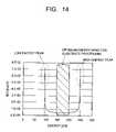
- FIG. 14is a graph showing a distribution status of ion energy that is suitable for RIE of the substrate S.
- the incident energy onto the substrate Sexhibits an ion energy distribution as shown in FIG. 13 .
- the ion energy in the plasma generated in the apparatus as shown in FIG. 11is divided in two, a low energy side peak and a high energy side peak, and an energy width ⁇ E thereof becomes as wide as a few tens to a few hundreds eV depending on the plasma generating condition. Therefore, even when Vdc is adjusted to energy that is optimum for substrate processing, there exist ions having energy that is too high (high energy side peak) and ions having energy that is too low (low energy side peak) among ions incident on the substrate as shown in FIG. 14 .
- the plasma generationis roughly classified into an inductive coupling type and a capacitive coupling type. From a viewpoint of fine control of processing shape, it is effective to shorten a residence time by reducing the plasma volume so as to suppress secondary reaction. In such a viewpoint, the parallel plate type plasma of capacitive coupling type is more advantageous as compared to the inductive coupling type plasma with a large volume.
- a method to introduce RFs with two different frequencies to parallel plate electrodes for independently controlling plasma density with a high frequency (100 MHz for example) RF and Vdc by a low frequency (3 MHz for example) RFfor example, refer to JP-A 2003-234331 (KOKAI)
- a high frequency power supply and a high frequency matching devicethere are provided a low frequency power supply and a low frequency matching device, thereby allowing superimposing of the aforementioned high frequency RF and low frequency RF with respect to the RF electrode.
- the counter electrodeis at the ground potential.
- Vdcgenerated on the counter electrode surface
- the two RFsare superimposed for the RF electrode on which the substrate is disposed.
- the present inventorsare considering applying DC negative pulses and a high frequency RF (HF) superimposedly.
- HFhigh frequency RF
- the band of positive ion energybecomes narrow and easily controllable to an energy band that is desirable for a process, thereby improving processing accuracy of plasma etching, suppressing plasma damage, and improving an embedding characteristic of plasma CVD.
- the radical densityis controlled by pulsing of HF (RF), and it is expected that plasma damage due to reduction of electron temperature is suppressed.
- the present inventionis made in view of the above-described conventional situation, and an object thereof is to provide a substrate plasma processing apparatus and a substrate plasma processing method which, in a plasma processing apparatus of what is called a parallel plate type, increase radical species density that is suitable for processing a substrate, and are capable of controlling the ion radical energy to an energy value and a narrow energy band which are suitable for processing a substrate to thereby perform fine processing, and further performing excellent embedding film forming.
- One aspect of a substrate plasma processing apparatusincludes a chamber capable of maintaining a vacuum therein, a first electrode to hold a substrate in the chamber, the substrate being processed on a main surface thereof, a counter electrode arranged to face the first electrode in the chamber, a first supply unit configured to apply a high frequency power having a predetermined frequency of 50 MHz or higher to the first electrode, a second supply unit configured to apply a predetermined DC negative pulse voltage in a manner of superimposing on the high frequency power to the first electrode, and a control unit controlling turning on or off of the first supply unit at a predetermined timing to thereby cause intermittent supply of the high frequency power, and controlling turning on or off of the second supply unit according to the timing of turning on or off of the first supply unit to thereby cause intermittent application of the DC negative pulse voltage.
- One aspect of a substrate plasma processing methoduses a substrate plasma processing apparatus which includes a chamber capable of maintaining a vacuum therein, a first electrode to hold a substrate in the chamber, the substrate being processed on a main surface thereof, a counter electrode arranged to face the first electrode in the chamber, a first supply unit configured to apply a high frequency power having a predetermined frequency of 50 MHz or higher to the first electrode, and a second supply unit configured to apply a predetermined DC negative pulse voltage in a manner of superimposing on the high frequency power to the first electrode, and the method includes turning on or off the high frequency power from the first supply unit at a predetermined timing to thereby cause intermittent application of the high frequency power, and turning on or off the second supply unit according to the timing of turning on or off of the high frequency power to thereby cause intermittent application of the DC negative pulse voltage.
- FIG. 1is a diagram showing the structure of a substrate plasma processing apparatus according to an embodiment of the present invention.
- FIG. 2is a diagram showing a substantial structure of the substrate plasma processing apparatus of FIG. 1 .
- FIG. 3is a diagram showing the structure of a modification example of the substantial structure of the substrate plasma processing apparatus of FIG. 1 .
- FIG. 4is a diagram showing the structure of a modification example of the substantial structure of the substrate plasma processing apparatus of FIG. 1 .
- FIG. 5is a chart showing timing of voltage application in the substrate plasma processing apparatus of FIG. 1 .
- FIG. 6is a chart showing timing of voltage application in the substrate plasma processing apparatus of FIG. 1 .
- FIG. 7Ais a chart showing simulation results of time variations of electron density and electron temperature in the embodiment
- FIG. 7Bis a chart showing high frequency power and a negative pulse voltage and an enlarged time axis thereof.
- FIG. 8Ais a chart showing fluorine radical density in the embodiment
- FIG. 8Bis a chart showing simulation results of etching rate in the embodiment.
- FIG. 9is a diagram for explaining occurrence of a charge-up.
- FIGS. 10A and 10Bare charts showing a relationship between DC pulse voltage application and a state of charge-up.
- FIG. 11is a diagram showing the structure of a plasma processing apparatus of parallel plate type.
- FIG. 12is a chart showing a relationship between RF power and a frequency and Vdc.
- FIG. 13is a graph showing a distribution of incident energy of ions into a substrate.
- FIG. 14is a graph showing a distribution state of ion energy suitable for a substrate.
- the substrate plasma processing apparatus 20 of this embodimentis a plasma processing apparatus of what is called a parallel plate type.
- a chamber 21capable of being evacuated to a predetermined degree of vacuum
- a substrate holding electrode (high frequency (RF) electrode) 22 and a counter electrode 23are arranged facing each other.
- a main surface of this substrate holding electrode 22 that faces the counter electrode 23is structured to be capable of holding a substrate S to be subjected to processing.
- a gas introducing pipe 24 and an exhaust port 25 connected to a not-shown vacuum pumpare provided in the chamber 21 . Then a gas to be used for generating plasma and thereby for processing the substrate S is introduced from the gas introducing pipe 24 into the chamber 21 as shown by arrows, and the inside of the chamber 21 is evacuated via the exhaust port 25 .
- a process gassuch as SF 6 , CF 4 , CH 3 F, C 2 F 6 , C 4 F 8 , C 5 F 8 , C 4 F 6 , Cl 2 , HBr, SiH 4 , or SiF 4 can be used appropriately.
- the pressure inside the chamber 21can be set appropriately according to the processing rate for the substrate S and the type of a used gas, and for example can be kept at approximately a few Pa.
- a high frequency generating device 27 and a DC negative pulse generating device 29are connected to the substrate holding electrode 22 . Further, a controller 30 is connected to the high frequency generating device 27 and the DC negative pulse generating device 29 , and this controller 30 controls operations of them. As its waveform being shown schematically in FIG. 1 , the high frequency generating device 27 generates a pulsed high frequency power (HF) having a predetermined frequency of 50 MHz or higher, and a pulsed DC negative pulse voltage is generated from the DC negative pulse generating device 29 . Then they are applied superimposedly to the substrate holding electrode 22 .
- HFpulsed high frequency power
- FIG. 2shows structures of the above-described high frequency generating device 27 and DC negative pulse generating device 29 .
- the high frequency generating device 27includes a high frequency oscillator 270 , a high frequency amplifier 271 , a matching device 272 , and a high-pass filter 273 .
- the high-pass filter 273is included in the matching device 272 .
- the DC negative pulse generating device 29includes a pulse oscillator 290 , a pulse amplifier 291 , and a low-pass filter 292 .
- the controller 30is formed by a trigger signal generator, and as shown by arrows in the diagram, a trigger signal A for the high frequency generating device 27 is inputted to the high frequency amplifier 271 , and a trigger signal B for the DC negative pulse generating device 29 is inputted to the pulse oscillator 290 . Then, the trigger signal A from the controller 30 causes the high frequency amplifier 271 to amplify the amplitude of a high frequency in a pulsed manner to thereby perform an on/off operation thereof. Further, the trigger signal B from the controller 30 causes the pulse oscillator 290 to perform an on/off operation of pulse generation.
- the amplified high frequencywhich is passed through the matching device 272 and the high-pass filter 273 for blocking an LF signal
- the DC negative pulses on the other handwhich are amplified by the pulse amplifier 291 and passed through the low-pass filter 292 for preventing reverse flow of signal, are applied superimposedly to the substrate holding electrode 22 .
- the trigger signal A for high frequency generation control and the trigger signal B for DC negative pulse generation controlare synchronized and controlled in timing in the controller 30 .
- Control of on/off operations of the high frequency and DC negative pulses by the controller 30 as described abovemay be performed as shown in FIG. 3 or FIG. 4 .
- the trigger signal A from the controller 30causes the high frequency amplifier 271 to amplify a high frequency amplitude in a pulsed manner to thereby perform an on/off operation thereof.
- the trigger signal B from the controller 30causes the pulse amplifier 291 to amplify a pulse amplitude in a pulsed manner to thereby perform an on/off operation.
- the trigger signal A from the controller 30causes the high-pass filter 273 to turn to an HF passing operation.
- the trigger signal B from the controller 30causes the low-pass filter 292 to turn to a pulse passing operation.
- Cutting or passing of signals in the filtersis performed by a variation of a variable element such as a capacitor or coil in the filters.
- control of on/off operations of the high frequency and DC negative pulsesis performed.
- the combination of control positionscan be selected freely for the trigger signal A from the controller 30 to control one of the high frequency oscillator 270 , the high frequency amplifier 271 , and the high-pass filter 273 to cause an on/off operation of the high frequency power and for the trigger signal B from the controller 30 to control one of the pulse oscillator 290 , the pulse amplifier 291 , and the low-pass filter 292 to cause an on/off operation of the DC negative pulse voltage.
- one of the high frequency oscillator 270 , the high frequency amplifier 271 , and the high-pass filter 273has an external trigger function, and a trigger signal B therefrom synchronously controls one of the pulse oscillator 290 , the pulse amplifier 291 , and the low-pass filter 292 , or that one of the pulse oscillator 290 , the pulse amplifier 291 , and the low-pass filter 292 has an external trigger function, and a trigger signal A therefrom synchronously controls one of the high frequency oscillator 270 , the high frequency amplifier 271 , and the high-pass filter 273 .
- off operations of the high frequency and the DC negative pulsesare preferred to be on/off operations in a pulsed manner, but the off operations may be amplitude varying operations which are different pulse-wise by ten times or more from the on operations.
- a 300 mm wafer for example as the substrate S on which a resist mask is formedis mounted on the substrate holding electrode 22 .
- the chamber 21is evacuated and a CF 4 gas for example as the predetermined processing gas is supplied from the counter electrode (shower head) 23 at a predetermined flow rate, 200 sccm for example.
- the degree of vacuum in the chamber 21is adjusted to a predetermined pressure, 2.66 Pa for example, by a not-shown exhaust valve.
- the high frequency from the high frequency generating device 27 and the DC negative pulses from the DC negative pulse generating device 29are applied superimposedly as shown in the block diagram of FIG. 1 and the timing chart of FIG. 5 .
- the high frequency from the high frequency generating device 27has a predetermined frequency of 50 MHz or higher, and for example a high frequency of 100 MHz and 100 V is used. As shown in FIG. 5 , this high frequency is on/off controlled at 50 ⁇ s intervals upon reception of the trigger signal A with a predetermined period and predetermined duty ratio, for example a 10 kHz period and 50% duty ratio, from the controller 30 . Further, from the DC negative pulse generating device 29 , DC negative pulses are generated with a predetermined repetition period and predetermined duty ratio, for example with a 1 MHz repetition period, 80% duty ratio, and ⁇ 500 V, and these DC negative pulses are on/off controlled at 50 ⁇ s intervals upon reception of the trigger signal B synchronized with the trigger signal A.
- these signalsare applied superimposedly to the substrate holding electrode 22 .
- the DC negative pulsesare turned on at the same time as turning on of the high frequency, and the DC negative pulses are turned off at the same time as turning off of the high frequency.
- FIG. 7Ashows time variations of the electron density and electron temperature when the pulsed high frequency and the DC negative pulses are applied superimposedly as described above.
- FIG. 7Bshows high frequency power and a negative pulse voltage and an enlarged time axe thereof.
- FIGS. 8A and 8 Bshow results of comparing the case of superimposedly applying the above-described pulsed high frequency and DC negative pulses and the case of typical high frequency plasma with respect to time variations of fluorine radical density and silicon substrate etching rate.
- these resultsare from simulating anisotropic etching rates of silicon oxide film by a CF 4 gas system using CHEMKIN made by Reaction Design.
- CHEMKINmade by Reaction Design.
- chemical reaction modelsmodels by Paulin Ho, et al. (J. Vac. Sci. Technol. A (2001)) are used.
- the DC negative pulsesare turned on at the same time as turning on of the high frequency, and the DC negative pulses are turned off at the same time as turning off of the high frequency.
- the DC negative pulseswill not be applied in the state of afterglow, and stable plasma is generated.
- the neutral fluorine radical density which deteriorates the processing shape by isotropic etchingdecreases.
- FIG. 8Bonly when the high frequency pulses and the DC negative pulses are applied, anisotropic etching of a silicon oxide film with less isotropic components providing an excellent processing shape was realized by cations with uniform energy widths (that is, the band thereof is narrowed). Further, in the system of etching to form a protective film, when the high frequency pulses and DC negative pulses are turned off, formation of the protective film occurs with no isotropic etching at all.
- FIG. 9shows only the case where the entire body is the insulator 100 , but it will be the same in the case where only the bottom portion is an insulator.
- Such a charge-upproceeds when the high frequency is stopped, and when the high frequency is present, it is alleviated or eliminated by ions and/or electrons with low energy.
- the DC negative pulsesare turned on at the same time as turning on of the high frequency, and the DC negative pulses are turned off at the same time as turning off of the high frequency.
- the charge-upis alleviated and eliminated by ions and electrons with low energy by application of the high frequency when application of the DC negative pulses is halted and only the high frequency is applied. That is, as shown in the timing chart of FIG. 6 , the charge-up in the trench portion is alleviated by halting application of the DC negative pulses a predetermined time T pre before the time of turning off of the high frequency.
- FIGS. 10A and 10Bshow that charge-up alleviation occurs as shown in FIG. 10B in the case where the DC negative pulses are applied intermittently as compared to the case where the DC negative pulses are applied sequentially as shown in FIG. 10A .
- pulse application timeis t 1 (seconds)
- pulse halt timeis t 3 (seconds)
- charge amount Y ⁇ n 1 ZeBN i v b t i per unit area that builds up during a sequential DC negative pulse application time (n 1 ⁇ t 1 (seconds) synchronized with the high frequency pulsesis suppressed equal to or less than an insulation limit charge amount Q max per unit area; and (2) to prevent occurrence of charge-up damage by charge accumulation due to charge-up when DC negative pulses are applied thereafter, charge alleviation amount ZeBN i v b T pre per unit area during application time (T pre (seconds)) of only the high frequency is equal to or larger than Q max . That is, it is necessary to control n 1 , t 1 , and T pre so as to satisfy the following expressions.
- ⁇ 0dielectric constant of vacuum
- ⁇ srelative dielectric constant of a trench bottom portion insulating material to be processed
- Zionic valency
- T eelectron temperature
- kBoltzmann's constant
- M iion mass
- dbottom portion insulating film thickness
- v maxwithstand voltage
- Bplasma density ratio of a sheath end portion and a bulk portion ( ⁇ 0.605)
- Yratio concerning charge accumulation when positive ions are incident
- eelementary electric charge
- N iis ion density.
- a recovery time of approximately 2 ⁇ sis required for allowing, by turning on of the high frequency, the electron temperature to recover to 1 ⁇ 2 of that when the high frequency is applied steadily.
- the DC negative pulsesare turned on before the electron temperature recovers, the plasma may become unstable. Then it is possible that the plasma disappears instantaneously, and inrush current stress when reigniting may cause damage to the device. Accordingly, as shown in FIG. 6 , for recovery and stabilization of plasma, the DC negative pulses are turned on when approximately 4 ⁇ s (T post ) passes after the high frequency is turned on, and thereby the plasma is stabilized further.
- T pre time, T post time, as well as pulse time T 1 , number of pulses n 1 , and duty ratio of DC negative pulses, and pulse frequency and duty ratio of HF according to the progress and switching of the plasma substrate processing processis effective for suppression of damage to the device, processing shape control, radical density control, and increase of the process rate.
Landscapes
- Physics & Mathematics (AREA)
- Engineering & Computer Science (AREA)
- Plasma & Fusion (AREA)
- Chemical & Material Sciences (AREA)
- Analytical Chemistry (AREA)
- Plasma Technology (AREA)
- Drying Of Semiconductors (AREA)
- Chemical Vapour Deposition (AREA)
Abstract
Description
- This application is based upon and claims the benefit of priority from the prior Japanese Patent Application No. 2008-023066, filed on Feb. 1, 2008; the entire contents of which are incorporated herein by reference.
- 1. Field of the Invention
- The present invention relates to a substrate plasma processing apparatus of what is called a parallel plate type and a substrate plasma processing method, in which an RF electrode and a counter electrode are arranged facing each other in a vacuum chamber and a substrate held on the RF electrode is processed with plasma generated between the electrodes.
- 2. Description of the Related Art
- When wiring or the like is performed on a substrate such as a semiconductor wafer, it is necessary to perform minute processing on the substrate. For this purpose, conventionally a plasma processing apparatus using plasma has been used frequently.
FIG. 11 is a diagram schematically showing the structure of an example of such a conventional substrate plasma processing apparatus.- The substrate
plasma processing apparatus 10 shown inFIG. 11 is a plasma processing apparatus of what is called a parallel plate type. In the substrateplasma processing apparatus 10, a high frequency (RF)electrode 12 and acounter electrode 13 are arranged facing each other in achamber 11. On a main surface of theRF electrode 12 that faces thecounter electrode 13, a substrate S to be subjected to processing is held. A gas to be used for generating plasma and thereby for processing the substrate S is introduced from agas introducing pipe 14 into thechamber 11 as shown by arrows. Along with this, a not-shown vacuum pump is used to evacuate the inside of thechamber 11 from anexhaust port 15. At this time, the pressure inside thechamber 11 is approximately 1 Pa for example. - Next, an RF (voltage) is applied to the
RF electrode 12 via amatching device 16 from a commercialRF power supply 17 of 13.56 MHz. Thus, plasma is generated between theRF electrode 12 and thecounter electrode 13. - At this time, positive ions in the plasma P are incident at high speed on the substrate S on the
RF electrode 12 by a negative self-bias potential Vdc generated on theRF electrode 12. Consequently, the substrate incident energy at this time is used to induce surface reaction on the substrate S to thereby perform plasma substrate processing such as reactive ion etching (RIE), plasma chemical vapor deposition (PCVD), sputtering, ion implantation, or the like. Particularly, from a viewpoint of processing a substrate, RIE is mainly used. Therefore, the explanation below will be given mainly focusing on substrate processing using RIE in particular. - In the plasma processing apparatus as shown in
FIG. 11 , Vdc (average substrate incident energy) increases as the RF power increases as shown inFIG. 12 . Accordingly, adjustment of the Vdc mainly by RF power is performed for adjusting a processing rate and adjusting a processing shape. Further, the Vdc can be partially adjusted also by the pressure or electrode shape on which the Vdc depends. FIG. 13 shows a result of simulating parallel plate type Ar plasma with a frequency of 13 MHz, Vrf=160 V, pressure of 6.6 Pa, 30 mm distance between electrodes and 300 mm wafer size by a continuum model plasma simulator (G. Chen, L. L. Raja, J. Appl. Phys. 96, 6073 (2004)) to obtain an ion energy distribution. Further,FIG. 14 is a graph showing a distribution status of ion energy that is suitable for RIE of the substrate S.- The incident energy onto the substrate S exhibits an ion energy distribution as shown in
FIG. 13 . As is clear fromFIG. 13 , the ion energy in the plasma generated in the apparatus as shown inFIG. 11 is divided in two, a low energy side peak and a high energy side peak, and an energy width ΔE thereof becomes as wide as a few tens to a few hundreds eV depending on the plasma generating condition. Therefore, even when Vdc is adjusted to energy that is optimum for substrate processing, there exist ions having energy that is too high (high energy side peak) and ions having energy that is too low (low energy side peak) among ions incident on the substrate as shown inFIG. 14 . - Therefore, in RIE for example, when substrate processing is implemented with ions having energy equivalent to the high energy side peak, there is a tendency to cause shoulder cutting (shoulder dropping) and deteriorate the processing shape. On the other hand, when substrate processing is implemented with ions having energy equivalent to the low energy side peak, it is equal to or lower than a surface reaction threshold and contributes nothing to the substrate processing or tends to deteriorate the processing shape accompanying deterioration of anisotropy (the ion incident angle widens by thermal velocity).
- In such a viewpoint, in semiconductor processes in these days, it is necessary to narrow the band of the ion energy (realization of small ΔE) as shown by hatching at a substantially center portion in
FIG. 14 and to optimally adjust an average energy value (optimization of Vdc) so as to finely control the processing shape corresponding to RIE of semiconductor devices, various films, and composite films, which are shrinking more and more. - To narrow the band of the ion energy, use of higher RF frequencies (for example, refer to JP-A 2003-234331 (KOKAI)) and use of pulse plasma (for example, refer to J. Appl. Phys. Vol. 88, No. 2, 643 (2000)) are considered.
- Further, the plasma generation is roughly classified into an inductive coupling type and a capacitive coupling type. From a viewpoint of fine control of processing shape, it is effective to shorten a residence time by reducing the plasma volume so as to suppress secondary reaction. In such a viewpoint, the parallel plate type plasma of capacitive coupling type is more advantageous as compared to the inductive coupling type plasma with a large volume.
- Further, for the purpose of improving controllability of Vdc and plasma density, there has been invented a method to introduce RFs with two different frequencies to parallel plate electrodes for independently controlling plasma density with a high frequency (100 MHz for example) RF and Vdc by a low frequency (3 MHz for example) RF (for example, refer to JP-A 2003-234331 (KOKAI)). In this case, in addition to a high frequency power supply and a high frequency matching device, there are provided a low frequency power supply and a low frequency matching device, thereby allowing superimposing of the aforementioned high frequency RF and low frequency RF with respect to the RF electrode.
- In viewpoints of cleaning process and process stabilization, it is advantageous that the counter electrode is at the ground potential. When an RF is applied to the counter electrode, the counter electrode is scraped by Vdc generated on the counter electrode surface, which becomes a dust source or a source of unstableness for the process. Therefore, the two RFs are superimposed for the RF electrode on which the substrate is disposed.
- Further, by pulsing of RF, there are attempted lowering of electron temperature (for example, refer to J. Appl. Phys. Vol. 86, No 9, pp 4813-4820 (1999)), suppressing of density of radicals disturbing the process (for example, fluorine radicals) (for example, refer to App. Phys. Lett., Vol. 63, No 15, pp. 2045-2046 (1993)), and improving selectivity of plasma etching (for example, a ratio of etching rate of silicon oxide/silicon) (for example, refer to J. Vac. Sci. Technol. A 13, pp 887-893 (1995)).
- As described above, conventionally it has been attempted to suppress plasma damage due to lowering of electron temperatures or the like by pulsing of a high frequency RF (HF), or superimposedly applying a high frequency RF (HF) and a low frequency RF (LF) to control radical density.
- Further, the present inventors are considering applying DC negative pulses and a high frequency RF (HF) superimposedly. In this technique, by superimposedly applying DC negative pulses, the band of positive ion energy becomes narrow and easily controllable to an energy band that is desirable for a process, thereby improving processing accuracy of plasma etching, suppressing plasma damage, and improving an embedding characteristic of plasma CVD. On the other hand, the radical density is controlled by pulsing of HF (RF), and it is expected that plasma damage due to reduction of electron temperature is suppressed.
- By superimposedly applying the DC negative pulses and the pulsed high frequency RF (HF), for example F radical density decreases (isotropic etching decreases) in anisotropic etching of an oxide film by a CF4gas, anisotropic etching by ion radicals of CF3+or the like increases, and moreover the ion energy is controlled to a narrow band. Further, the radical density of CF2or the like increases, which becomes a generation source of a side wall protective film (facilitation of anisotropy). With these radical species selecting effect and energy selecting effect, remarkable improvement in processing performance together with improvement in process controllability are realized.
- However, as shown in
FIGS. 7A and 7B which will be explained later (analytical results of simulating plasma density, electron temperature, and time variation of a process when a pulsed HF and DC negative pluses are applied superimposedly), the electron temperature lowers in a quite short time (5×10⁻⁶seconds or shorter) as the high frequency power (HF) turns off, and generation of ions and electrons by electronic collision and ionization stops. In this what is called an afterglow state, when the DC negative pulses are applied, electrons and ions in the plasma are drawn out of the plasma, and the plasma becomes unstable and disappears. The disappearance of the plasma causes reduction of the process rate, device damage when reignition, and process unstabilization. Further, as shown inFIG. 9 , when processing aninsulator 100 such as an oxide film or a nitride film using the DC negative pulses, it is possible that a charge-up due to insufficiency of electrons occurs in abottom portion 102 of atrench 101. When such a charge-up occurs, it then causes deterioration of processing shape due to ion drflection, etching stop, or damage to the device due to a charge voltage. - The present invention is made in view of the above-described conventional situation, and an object thereof is to provide a substrate plasma processing apparatus and a substrate plasma processing method which, in a plasma processing apparatus of what is called a parallel plate type, increase radical species density that is suitable for processing a substrate, and are capable of controlling the ion radical energy to an energy value and a narrow energy band which are suitable for processing a substrate to thereby perform fine processing, and further performing excellent embedding film forming.
- One aspect of a substrate plasma processing apparatus according to the present invention includes a chamber capable of maintaining a vacuum therein, a first electrode to hold a substrate in the chamber, the substrate being processed on a main surface thereof, a counter electrode arranged to face the first electrode in the chamber, a first supply unit configured to apply a high frequency power having a predetermined frequency of 50 MHz or higher to the first electrode, a second supply unit configured to apply a predetermined DC negative pulse voltage in a manner of superimposing on the high frequency power to the first electrode, and a control unit controlling turning on or off of the first supply unit at a predetermined timing to thereby cause intermittent supply of the high frequency power, and controlling turning on or off of the second supply unit according to the timing of turning on or off of the first supply unit to thereby cause intermittent application of the DC negative pulse voltage.
- One aspect of a substrate plasma processing method according to the present invention uses a substrate plasma processing apparatus which includes a chamber capable of maintaining a vacuum therein, a first electrode to hold a substrate in the chamber, the substrate being processed on a main surface thereof, a counter electrode arranged to face the first electrode in the chamber, a first supply unit configured to apply a high frequency power having a predetermined frequency of 50 MHz or higher to the first electrode, and a second supply unit configured to apply a predetermined DC negative pulse voltage in a manner of superimposing on the high frequency power to the first electrode, and the method includes turning on or off the high frequency power from the first supply unit at a predetermined timing to thereby cause intermittent application of the high frequency power, and turning on or off the second supply unit according to the timing of turning on or off of the high frequency power to thereby cause intermittent application of the DC negative pulse voltage.
FIG. 1 is a diagram showing the structure of a substrate plasma processing apparatus according to an embodiment of the present invention.FIG. 2 is a diagram showing a substantial structure of the substrate plasma processing apparatus ofFIG. 1 .FIG. 3 is a diagram showing the structure of a modification example of the substantial structure of the substrate plasma processing apparatus ofFIG. 1 .FIG. 4 is a diagram showing the structure of a modification example of the substantial structure of the substrate plasma processing apparatus ofFIG. 1 .FIG. 5 is a chart showing timing of voltage application in the substrate plasma processing apparatus ofFIG. 1 .FIG. 6 is a chart showing timing of voltage application in the substrate plasma processing apparatus ofFIG. 1 .FIG. 7A is a chart showing simulation results of time variations of electron density and electron temperature in the embodiment;FIG. 7B is a chart showing high frequency power and a negative pulse voltage and an enlarged time axis thereof.FIG. 8A is a chart showing fluorine radical density in the embodiment;FIG. 8B is a chart showing simulation results of etching rate in the embodiment.FIG. 9 is a diagram for explaining occurrence of a charge-up.FIGS. 10A and 10B are charts showing a relationship between DC pulse voltage application and a state of charge-up.FIG. 11 is a diagram showing the structure of a plasma processing apparatus of parallel plate type.FIG. 12 is a chart showing a relationship between RF power and a frequency and Vdc.FIG. 13 is a graph showing a distribution of incident energy of ions into a substrate.FIG. 14 is a graph showing a distribution state of ion energy suitable for a substrate.- Hereinafter, embodiments of a substrate plasma processing apparatus and a substrate plasma processing method according to the present invention will be explained with reference to the drawings. First, an embodiment of the substrate plasma processing apparatus will be explained with reference to
FIG. 1 . - As shown in
FIG. 1 , the substrateplasma processing apparatus 20 of this embodiment is a plasma processing apparatus of what is called a parallel plate type. In achamber 21 capable of being evacuated to a predetermined degree of vacuum, a substrate holding electrode (high frequency (RF) electrode)22 and acounter electrode 23 are arranged facing each other. A main surface of thissubstrate holding electrode 22 that faces thecounter electrode 23 is structured to be capable of holding a substrate S to be subjected to processing. In thechamber 21, agas introducing pipe 24 and anexhaust port 25 connected to a not-shown vacuum pump are provided. Then a gas to be used for generating plasma and thereby for processing the substrate S is introduced from thegas introducing pipe 24 into thechamber 21 as shown by arrows, and the inside of thechamber 21 is evacuated via theexhaust port 25. - As the above gas, besides a gas of Ar, Kr, Xe, N2, O2, CO, or H2, for example, a process gas such as SF6, CF4, CH3F, C2F6, C4F8, C5F8, C4F6, Cl2, HBr, SiH4, or SiF4can be used appropriately. Further, the pressure inside the
chamber 21 can be set appropriately according to the processing rate for the substrate S and the type of a used gas, and for example can be kept at approximately a few Pa. - To the
substrate holding electrode 22, a highfrequency generating device 27 and a DC negativepulse generating device 29 are connected. Further, acontroller 30 is connected to the highfrequency generating device 27 and the DC negativepulse generating device 29, and thiscontroller 30 controls operations of them. As its waveform being shown schematically inFIG. 1 , the highfrequency generating device 27 generates a pulsed high frequency power (HF) having a predetermined frequency of 50 MHz or higher, and a pulsed DC negative pulse voltage is generated from the DC negativepulse generating device 29. Then they are applied superimposedly to thesubstrate holding electrode 22. FIG. 2 shows structures of the above-described highfrequency generating device 27 and DC negativepulse generating device 29. As shown in this diagram, the highfrequency generating device 27 includes ahigh frequency oscillator 270, ahigh frequency amplifier 271, amatching device 272, and a high-pass filter 273. In addition, it is possible that the high-pass filter 273 is included in thematching device 272. Further, the DC negativepulse generating device 29 includes apulse oscillator 290, apulse amplifier 291, and a low-pass filter 292.- The
controller 30 is formed by a trigger signal generator, and as shown by arrows in the diagram, a trigger signal A for the highfrequency generating device 27 is inputted to thehigh frequency amplifier 271, and a trigger signal B for the DC negativepulse generating device 29 is inputted to thepulse oscillator 290. Then, the trigger signal A from thecontroller 30 causes thehigh frequency amplifier 271 to amplify the amplitude of a high frequency in a pulsed manner to thereby perform an on/off operation thereof. Further, the trigger signal B from thecontroller 30 causes thepulse oscillator 290 to perform an on/off operation of pulse generation. Then the amplified high frequency, which is passed through thematching device 272 and the high-pass filter 273 for blocking an LF signal, and the DC negative pulses on the other hand, which are amplified by thepulse amplifier 291 and passed through the low-pass filter 292 for preventing reverse flow of signal, are applied superimposedly to thesubstrate holding electrode 22. The trigger signal A for high frequency generation control and the trigger signal B for DC negative pulse generation control are synchronized and controlled in timing in thecontroller 30. - Control of on/off operations of the high frequency and DC negative pulses by the
controller 30 as described above may be performed as shown inFIG. 3 orFIG. 4 . In the case shown inFIG. 3 , the trigger signal A from thecontroller 30 causes thehigh frequency amplifier 271 to amplify a high frequency amplitude in a pulsed manner to thereby perform an on/off operation thereof. Further, the trigger signal B from thecontroller 30 causes thepulse amplifier 291 to amplify a pulse amplitude in a pulsed manner to thereby perform an on/off operation. Further, in the case shown inFIG. 4 , the trigger signal A from thecontroller 30 causes the high-pass filter 273 to turn to an HF passing operation. Further, the trigger signal B from thecontroller 30 causes the low-pass filter 292 to turn to a pulse passing operation. Cutting or passing of signals in the filters is performed by a variation of a variable element such as a capacitor or coil in the filters. Thus, control of on/off operations of the high frequency and DC negative pulses is performed. - Besides them, although not shown, the combination of control positions can be selected freely for the trigger signal A from the
controller 30 to control one of thehigh frequency oscillator 270, thehigh frequency amplifier 271, and the high-pass filter 273 to cause an on/off operation of the high frequency power and for the trigger signal B from thecontroller 30 to control one of thepulse oscillator 290, thepulse amplifier 291, and the low-pass filter 292 to cause an on/off operation of the DC negative pulse voltage. - Further, it is also possible that one of the
high frequency oscillator 270, thehigh frequency amplifier 271, and the high-pass filter 273 has an external trigger function, and a trigger signal B therefrom synchronously controls one of thepulse oscillator 290, thepulse amplifier 291, and the low-pass filter 292, or that one of thepulse oscillator 290, thepulse amplifier 291, and the low-pass filter 292 has an external trigger function, and a trigger signal A therefrom synchronously controls one of thehigh frequency oscillator 270, thehigh frequency amplifier 271, and the high-pass filter 273. Further, off operations of the high frequency and the DC negative pulses are preferred to be on/off operations in a pulsed manner, but the off operations may be amplitude varying operations which are different pulse-wise by ten times or more from the on operations. - When substrate plasma processing is performed by the substrate
plasma processing apparatus 20 having the above structure, a 300 mm wafer for example as the substrate S on which a resist mask is formed is mounted on thesubstrate holding electrode 22. Next, thechamber 21 is evacuated and a CF4gas for example as the predetermined processing gas is supplied from the counter electrode (shower head)23 at a predetermined flow rate, 200 sccm for example. Then the degree of vacuum in thechamber 21 is adjusted to a predetermined pressure, 2.66 Pa for example, by a not-shown exhaust valve. Onto thesubstrate holding electrode 22 on which the wafer is mounted, the high frequency from the highfrequency generating device 27 and the DC negative pulses from the DC negativepulse generating device 29 are applied superimposedly as shown in the block diagram ofFIG. 1 and the timing chart ofFIG. 5 . - The high frequency from the high
frequency generating device 27 has a predetermined frequency of 50 MHz or higher, and for example a high frequency of 100 MHz and 100 V is used. As shown inFIG. 5 , this high frequency is on/off controlled at 50 μs intervals upon reception of the trigger signal A with a predetermined period and predetermined duty ratio, for example a 10 kHz period and 50% duty ratio, from thecontroller 30. Further, from the DC negativepulse generating device 29, DC negative pulses are generated with a predetermined repetition period and predetermined duty ratio, for example with a 1 MHz repetition period, 80% duty ratio, and −500 V, and these DC negative pulses are on/off controlled at 50 μs intervals upon reception of the trigger signal B synchronized with the trigger signal A. As shown at the lowest part ofFIG. 5 , these signals are applied superimposedly to thesubstrate holding electrode 22. In the timing chart shown inFIG. 5 , the DC negative pulses are turned on at the same time as turning on of the high frequency, and the DC negative pulses are turned off at the same time as turning off of the high frequency. FIG. 7A shows time variations of the electron density and electron temperature when the pulsed high frequency and the DC negative pulses are applied superimposedly as described above. In addition,FIG. 7B shows high frequency power and a negative pulse voltage and an enlarged time axe thereof. Further,FIGS. 8A and8B show results of comparing the case of superimposedly applying the above-described pulsed high frequency and DC negative pulses and the case of typical high frequency plasma with respect to time variations of fluorine radical density and silicon substrate etching rate. In addition, these results are from simulating anisotropic etching rates of silicon oxide film by a CF4gas system using CHEMKIN made by Reaction Design. As chemical reaction models, models by Paulin Ho, et al. (J. Vac. Sci. Technol. A (2001)) are used.- As shown in
FIG. 7A , when the pulsed high frequency and DC negative pulses are applied superimposedly as in the timing chart shown inFIG. 5 , stable plasma is generated. That is, as described above, the electron temperature lowers quickly (by 5×10⁻⁶seconds or shorter) as the high frequency power (HF) turns off, and generation of ions and electrons by electronic collision and ionization stops. In this what is called an afterglow state, when the DC negative pulses are applied, electrons and ions in the plasma are drawn out of the plasma, and the plasma becomes unstable and disappears. The disappearance of the plasma then causes reduction of the process rate, device damage when reignition, and process unstabilization. On the other hand, as shown in the timing chart ofFIG. 5 , in this embodiment, the DC negative pulses are turned on at the same time as turning on of the high frequency, and the DC negative pulses are turned off at the same time as turning off of the high frequency. Thus, the DC negative pulses will not be applied in the state of afterglow, and stable plasma is generated. - Further, as shown in
FIG. 8A , along with lowering of the electron temperature (lowering of average electron temperature) when the high frequency is turned off, the neutral fluorine radical density which deteriorates the processing shape by isotropic etching decreases. As shown inFIG. 8B , only when the high frequency pulses and the DC negative pulses are applied, anisotropic etching of a silicon oxide film with less isotropic components providing an excellent processing shape was realized by cations with uniform energy widths (that is, the band thereof is narrowed). Further, in the system of etching to form a protective film, when the high frequency pulses and DC negative pulses are turned off, formation of the protective film occurs with no isotropic etching at all. - Further, as shown in
FIG. 9 , when aninsulator 100 is etched with plasma in which DC negative pulses are superimposed, there occurs a small flux of electrons showering in an isotropic manner on abottom portion 102 of atrench 101 having a large aspect ratio, and thus a positive charge build-up (charge-up) occurs in theinsulator 100 on thebottom portion 102. Low energy ions decrease when the DC negative pulses are used, and thus the charge-up increases further. In addition, in anupper side wall 103 of thetrench 101, a negative charge-up (instantaneous) occurs by an excessive electron flux. Accordingly, by the charge-up in thebottom portion 102 of thetrench 101, the path of incident positive ions are deflected and the anisotropy deteriorates. Consequently, deterioration of processing accuracy, deterioration of an embedding characteristic, and etching stop occur, thereby causing damage. Note thatFIG. 9 shows only the case where the entire body is theinsulator 100, but it will be the same in the case where only the bottom portion is an insulator. Such a charge-up proceeds when the high frequency is stopped, and when the high frequency is present, it is alleviated or eliminated by ions and/or electrons with low energy. - As shown in the timing chart of
FIG. 5 , in this embodiment the DC negative pulses are turned on at the same time as turning on of the high frequency, and the DC negative pulses are turned off at the same time as turning off of the high frequency. Thus, it will not happen that only the DC negative pulses are applied during the high frequency is stopped, and occurrence of the charge-up as described above can be suppressed. - Further, in this case, the charge-up is alleviated and eliminated by ions and electrons with low energy by application of the high frequency when application of the DC negative pulses is halted and only the high frequency is applied. That is, as shown in the timing chart of
FIG. 6 , the charge-up in the trench portion is alleviated by halting application of the DC negative pulses a predetermined time Tprebefore the time of turning off of the high frequency. FIGS. 10A and 10B show that charge-up alleviation occurs as shown inFIG. 10B in the case where the DC negative pulses are applied intermittently as compared to the case where the DC negative pulses are applied sequentially as shown inFIG. 10A . As shown in theseFIGS. 10A and 10B , when the number of sequentially applied DC negative pulses is n1, pulse application time is t1(seconds), and pulse halt time is t3(seconds), for preventing charge-up damage it is necessary that:- (1) charge amount Y·n1ZeBNivbtiper unit area that builds up during a sequential DC negative pulse application time (n1×t1(seconds) synchronized with the high frequency pulses is suppressed equal to or less than an insulation limit charge amount Qmaxper unit area; and
(2) to prevent occurrence of charge-up damage by charge accumulation due to charge-up when DC negative pulses are applied thereafter, charge alleviation amount ZeBNivbTpreper unit area during application time (Tpre(seconds)) of only the high frequency is equal to or larger than Qmax. That is, it is necessary to control n1, t1, and Tpreso as to satisfy the following expressions.
Y·n1ZeBNivbt1≦Qmax (1)
Qmax=Vmax*(ε0εs/d5) (2)- Here, ε0is dielectric constant of vacuum, εsis relative dielectric constant of a trench bottom portion insulating material to be processed, Z is ionic valency, vbis Bohm speed as vb=(kTe/Mi)1/2, Teis electron temperature, k is Boltzmann's constant, Miis ion mass, d is bottom portion insulating film thickness, vmaxis withstand voltage, B is plasma density ratio of a sheath end portion and a bulk portion (≈0.605), Y is ratio concerning charge accumulation when positive ions are incident, e is elementary electric charge, and Niis ion density.
- Taking processing of a gate oxide film as an example, when a
gate width 50 nm, d=10 nm, and a typical destruction withstandvoltage 10 MV/cm of an oxide film are used, Vmax=10 V and Qmax=3.54×10⁻²[C/m2] hold true. From expression (2), Tpre≧5.18 [μs] holds true. - Further, in the case of DC pulses with a repetition frequency of 1 MHz (t1=1 μs) and 80% duty ratio, Y≈0.6 is estimated when adding the duty ratio, resulting in Y·ZeBNivbt1in expression (1)=3.28×10⁻³[C/m2]. Specifically, when t1·n1≦10.8 μs and the repetition period of the high frequency pulses of 50% duty ratio is 50 kHz or larger, expression (1) is satisfied and no damage will be caused.
- Further, as shown in
FIG. 7A , a recovery time of approximately 2 μs is required for allowing, by turning on of the high frequency, the electron temperature to recover to ½ of that when the high frequency is applied steadily. When the DC negative pulses are turned on before the electron temperature recovers, the plasma may become unstable. Then it is possible that the plasma disappears instantaneously, and inrush current stress when reigniting may cause damage to the device. Accordingly, as shown inFIG. 6 , for recovery and stabilization of plasma, the DC negative pulses are turned on when approximately 4 μs (Tpost) passes after the high frequency is turned on, and thereby the plasma is stabilized further. - Further, changing of the above Tpretime, Tposttime, as well as pulse time T1, number of pulses n1, and duty ratio of DC negative pulses, and pulse frequency and duty ratio of HF according to the progress and switching of the plasma substrate processing process is effective for suppression of damage to the device, processing shape control, radical density control, and increase of the process rate.
- It should be noted that the present invention is not limited to the above-described embodiments, and as a matter of course, various modifications can be made. Further, the embodiments of the present invention can be extended or changed within the scope of the technical idea of the present invention, and these extended and/or modified embodiments are to be included in the technical scope of the present invention. Additional advantages and modifications will readily occur to those skilled in the art. Therefore, the invention in its broader aspects is not limited to the specific details and representative embodiments shown and described herein. Accordingly, various modifications may be made without departing from the spirit or scope of the general inventive concept as defined by the appended claims and their equivalents.
Claims (7)
Applications Claiming Priority (2)
| Application Number | Priority Date | Filing Date | Title |
|---|---|---|---|
| JPP2008-023066 | 2008-02-01 | ||
| JP2008023066AJP5224837B2 (en) | 2008-02-01 | 2008-02-01 | Substrate plasma processing apparatus and plasma processing method |
Publications (2)
| Publication Number | Publication Date |
|---|---|
| US20090194508A1true US20090194508A1 (en) | 2009-08-06 |
| US8821684B2 US8821684B2 (en) | 2014-09-02 |
Family
ID=40930646
Family Applications (1)
| Application Number | Title | Priority Date | Filing Date |
|---|---|---|---|
| US12/363,070Active2031-05-16US8821684B2 (en) | 2008-02-01 | 2009-01-30 | Substrate plasma processing apparatus and plasma processing method |
Country Status (5)
| Country | Link |
|---|---|
| US (1) | US8821684B2 (en) |
| JP (1) | JP5224837B2 (en) |
| KR (1) | KR101051243B1 (en) |
| CN (1) | CN101499399B (en) |
| TW (1) | TWI402909B (en) |
Cited By (67)
| Publication number | Priority date | Publication date | Assignee | Title |
|---|---|---|---|---|
| US20100072172A1 (en)* | 2008-09-24 | 2010-03-25 | Akio Ui | Substrate processing apparatus and substrate processing method |
| US20120052689A1 (en)* | 2010-09-01 | 2012-03-01 | Samsung Electronics Co., Ltd. | Plasma etching method and apparatus thereof |
| US20120048831A1 (en)* | 2010-08-24 | 2012-03-01 | Micron Technology, Inc. | Methods and apparatuses for energetic neutral flux generation for processing a substrate |
| US20120247677A1 (en)* | 2011-03-31 | 2012-10-04 | Tokyo Electron Limited | Substrate processing method |
| US8821744B2 (en) | 2010-09-30 | 2014-09-02 | Kabushiki Kaisha Toshiba | Substrate processing method and substrate processing apparatus |
| US20140251956A1 (en)* | 2013-03-06 | 2014-09-11 | Samsung Electronics Co., Ltd. | Etching apparatus and etching method |
| US9583360B2 (en) | 2009-09-29 | 2017-02-28 | Kabushiki Kaisha Toshiba | Substrate processing apparatus and substrate processing method |
| US20180082861A1 (en)* | 2016-06-29 | 2018-03-22 | Applied Materials, Inc. | Selective etch using material modification and rf pulsing |
| US10181412B2 (en)* | 2011-07-21 | 2019-01-15 | Lam Research Corporation | Negative ion control for dielectric etch |
| US20190057845A1 (en)* | 2017-08-18 | 2019-02-21 | Tokyo Electron Limited | Plasma processing method and plasma processing apparatus |
| US10373804B2 (en)* | 2017-02-03 | 2019-08-06 | Applied Materials, Inc. | System for tunable workpiece biasing in a plasma reactor |
| CN110391126A (en)* | 2018-04-20 | 2019-10-29 | 应用材料公司 | Phased Array Modular High Frequency Source |
| CN110416116A (en)* | 2018-04-27 | 2019-11-05 | 东京毅力科创株式会社 | Etching apparatus and etching method |
| US10529737B2 (en) | 2017-02-08 | 2020-01-07 | Applied Materials, Inc. | Accommodating imperfectly aligned memory holes |
| US10541113B2 (en) | 2016-10-04 | 2020-01-21 | Applied Materials, Inc. | Chamber with flow-through source |
| US10573527B2 (en) | 2018-04-06 | 2020-02-25 | Applied Materials, Inc. | Gas-phase selective etching systems and methods |
| US10607867B2 (en) | 2015-08-06 | 2020-03-31 | Applied Materials, Inc. | Bolted wafer chuck thermal management systems and methods for wafer processing systems |
| US10615047B2 (en) | 2018-02-28 | 2020-04-07 | Applied Materials, Inc. | Systems and methods to form airgaps |
| US10699921B2 (en) | 2018-02-15 | 2020-06-30 | Applied Materials, Inc. | Semiconductor processing chamber multistage mixing apparatus |
| US10704149B2 (en) | 2014-06-10 | 2020-07-07 | Lam Research Corporation | Defect control and stability of DC bias in RF plasma-based substrate processing systems using molecular reactive purge gas |
| US10707058B2 (en) | 2017-04-11 | 2020-07-07 | Applied Materials, Inc. | Symmetric and irregular shaped plasmas using modular microwave sources |
| US10748745B2 (en) | 2016-08-16 | 2020-08-18 | Applied Materials, Inc. | Modular microwave plasma source |
| US10770346B2 (en) | 2016-11-11 | 2020-09-08 | Applied Materials, Inc. | Selective cobalt removal for bottom up gapfill |
| US10796922B2 (en) | 2014-10-14 | 2020-10-06 | Applied Materials, Inc. | Systems and methods for internal surface conditioning assessment in plasma processing equipment |
| US10854426B2 (en) | 2018-01-08 | 2020-12-01 | Applied Materials, Inc. | Metal recess for semiconductor structures |
| US10886137B2 (en) | 2018-04-30 | 2021-01-05 | Applied Materials, Inc. | Selective nitride removal |
| US10892198B2 (en) | 2018-09-14 | 2021-01-12 | Applied Materials, Inc. | Systems and methods for improved performance in semiconductor processing |
| US10903052B2 (en) | 2017-02-03 | 2021-01-26 | Applied Materials, Inc. | Systems and methods for radial and azimuthal control of plasma uniformity |
| US10903054B2 (en) | 2017-12-19 | 2021-01-26 | Applied Materials, Inc. | Multi-zone gas distribution systems and methods |
| US10920319B2 (en) | 2019-01-11 | 2021-02-16 | Applied Materials, Inc. | Ceramic showerheads with conductive electrodes |
| US10943834B2 (en) | 2017-03-13 | 2021-03-09 | Applied Materials, Inc. | Replacement contact process |
| US10964512B2 (en) | 2018-02-15 | 2021-03-30 | Applied Materials, Inc. | Semiconductor processing chamber multistage mixing apparatus and methods |
| US11004689B2 (en) | 2018-03-12 | 2021-05-11 | Applied Materials, Inc. | Thermal silicon etch |
| US11024486B2 (en) | 2013-02-08 | 2021-06-01 | Applied Materials, Inc. | Semiconductor processing systems having multiple plasma configurations |
| US11037764B2 (en) | 2017-05-06 | 2021-06-15 | Applied Materials, Inc. | Modular microwave source with local Lorentz force |
| US20210183622A1 (en)* | 2019-12-17 | 2021-06-17 | Tokyo Electron Limited | Plasma processing apparatus and plasma processing method |
| US11049698B2 (en) | 2016-10-04 | 2021-06-29 | Applied Materials, Inc. | Dual-channel showerhead with improved profile |
| US11049755B2 (en) | 2018-09-14 | 2021-06-29 | Applied Materials, Inc. | Semiconductor substrate supports with embedded RF shield |
| US11062887B2 (en) | 2018-09-17 | 2021-07-13 | Applied Materials, Inc. | High temperature RF heater pedestals |
| US11081317B2 (en) | 2018-04-20 | 2021-08-03 | Applied Materials, Inc. | Modular high-frequency source |
| US11101136B2 (en) | 2017-08-07 | 2021-08-24 | Applied Materials, Inc. | Process window widening using coated parts in plasma etch processes |
| US11121002B2 (en) | 2018-10-24 | 2021-09-14 | Applied Materials, Inc. | Systems and methods for etching metals and metal derivatives |
| US11158527B2 (en) | 2015-08-06 | 2021-10-26 | Applied Materials, Inc. | Thermal management systems and methods for wafer processing systems |
| US20210398774A1 (en)* | 2018-10-24 | 2021-12-23 | Jiangsu Leuven Instruments Co. Ltd | Etching device and method of inductively coupled plasma |
| US11224116B2 (en)* | 2017-10-18 | 2022-01-11 | Lam Research Corporation | Matchless plasma source for semiconductor wafer fabrication |
| US11239061B2 (en) | 2014-11-26 | 2022-02-01 | Applied Materials, Inc. | Methods and systems to enhance process uniformity |
| US11264213B2 (en) | 2012-09-21 | 2022-03-01 | Applied Materials, Inc. | Chemical control features in wafer process equipment |
| US11276559B2 (en) | 2017-05-17 | 2022-03-15 | Applied Materials, Inc. | Semiconductor processing chamber for multiple precursor flow |
| US11328909B2 (en) | 2017-12-22 | 2022-05-10 | Applied Materials, Inc. | Chamber conditioning and removal processes |
| US11393661B2 (en) | 2018-04-20 | 2022-07-19 | Applied Materials, Inc. | Remote modular high-frequency source |
| US11417534B2 (en) | 2018-09-21 | 2022-08-16 | Applied Materials, Inc. | Selective material removal |
| US11437242B2 (en) | 2018-11-27 | 2022-09-06 | Applied Materials, Inc. | Selective removal of silicon-containing materials |
| US11476093B2 (en) | 2015-08-27 | 2022-10-18 | Applied Materials, Inc. | Plasma etching systems and methods with secondary plasma injection |
| US11594428B2 (en) | 2015-02-03 | 2023-02-28 | Applied Materials, Inc. | Low temperature chuck for plasma processing systems |
| US11682560B2 (en) | 2018-10-11 | 2023-06-20 | Applied Materials, Inc. | Systems and methods for hafnium-containing film removal |
| US11721527B2 (en) | 2019-01-07 | 2023-08-08 | Applied Materials, Inc. | Processing chamber mixing systems |
| US11735441B2 (en) | 2016-05-19 | 2023-08-22 | Applied Materials, Inc. | Systems and methods for improved semiconductor etching and component protection |
| US20230402256A1 (en)* | 2022-06-09 | 2023-12-14 | Tokyo Electron Limited | Plasma processing method and substrate processing apparatus |
| US11887817B2 (en) | 2020-04-28 | 2024-01-30 | Tokyo Electron Limited | Plasma processing apparatus and plasma processing method |
| US11915950B2 (en) | 2017-05-17 | 2024-02-27 | Applied Materials, Inc. | Multi-zone semiconductor substrate supports |
| US20240096594A1 (en)* | 2022-09-19 | 2024-03-21 | Adaptive Plasma Technology Corp. | System for etching with a plasma |
| EP4150661A4 (en)* | 2020-05-12 | 2024-05-29 | Eagle Harbor Technologies, Inc. | HIGH FREQUENCY RF GENERATOR AND DC PULSATION |
| US12027344B2 (en) | 2018-06-13 | 2024-07-02 | Tokyo Electron Limited | Film forming apparatus |
| US12198898B2 (en) | 2018-11-30 | 2025-01-14 | Eagle Harbor Technologies, Inc. | Variable output impedance RF generator |
| US12334305B2 (en) | 2020-03-17 | 2025-06-17 | Tokyo Electron Limited | Plasma processing apparatus |
| US12340979B2 (en) | 2017-05-17 | 2025-06-24 | Applied Materials, Inc. | Semiconductor processing chamber for improved precursor flow |
| US12400832B2 (en) | 2020-04-28 | 2025-08-26 | Tokyo Electron Limited | Plasma processing apparatus and plasma processing method |
Families Citing this family (50)
| Publication number | Priority date | Publication date | Assignee | Title |
|---|---|---|---|---|
| KR101214758B1 (en)* | 2010-02-26 | 2012-12-21 | 성균관대학교산학협력단 | Etching Method |
| JP2012104382A (en)* | 2010-11-10 | 2012-05-31 | Tokyo Electron Ltd | Plasma treatment apparatus, plasma treatment method, and plasma treatment bias voltage determination method |
| JP5977509B2 (en)* | 2011-12-09 | 2016-08-24 | 東京エレクトロン株式会社 | Plasma processing method and plasma processing apparatus |
| CN103632913B (en)* | 2012-08-28 | 2016-06-22 | 中微半导体设备(上海)有限公司 | Plasma processing apparatus |
| CN103730316B (en)* | 2012-10-16 | 2016-04-06 | 中微半导体设备(上海)有限公司 | A kind of plasma processing method and plasma treatment appts |
| CN103021783B (en)* | 2012-12-24 | 2015-12-02 | 中微半导体设备(上海)有限公司 | The lithographic method of semiconductor structure |
| CN103746674B (en)* | 2013-12-25 | 2017-01-11 | 北京长峰广播通讯设备有限责任公司 | Method and apparatus for generating self-excited oscillation type electronic tube grid modulation pulse |
| JP6579786B2 (en)* | 2015-04-17 | 2019-09-25 | 株式会社日立ハイテクノロジーズ | Plasma etching method |
| US9799491B2 (en)* | 2015-10-29 | 2017-10-24 | Applied Materials, Inc. | Low electron temperature etch chamber with independent control over plasma density, radical composition and ion energy for atomic precision etching |
| US10779980B2 (en) | 2016-04-27 | 2020-09-22 | Synerz Medical, Inc. | Intragastric device for treating obesity |
| KR102476353B1 (en)* | 2016-07-26 | 2022-12-09 | 삼성전자주식회사 | Designed waveform generator for semiconductor equipment, plasma processing apparatus, method of controlling plasma processing apparatus, and method of manufacturing semiconductor device |
| JP6903375B2 (en) | 2017-04-19 | 2021-07-14 | 株式会社ディスコ | Device chip manufacturing method |
| US10510575B2 (en) | 2017-09-20 | 2019-12-17 | Applied Materials, Inc. | Substrate support with multiple embedded electrodes |
| US20240079213A9 (en) | 2017-11-17 | 2024-03-07 | Advanced Energy Industries, Inc. | Synchronization of plasma processing components |
| KR102730398B1 (en)* | 2017-12-07 | 2024-11-13 | 램 리써치 코포레이션 | Rf pulsing within pulsing for semiconductor rf plasma processing |
| US10555412B2 (en) | 2018-05-10 | 2020-02-04 | Applied Materials, Inc. | Method of controlling ion energy distribution using a pulse generator with a current-return output stage |
| US11476145B2 (en) | 2018-11-20 | 2022-10-18 | Applied Materials, Inc. | Automatic ESC bias compensation when using pulsed DC bias |
| KR102827481B1 (en) | 2019-01-22 | 2025-06-30 | 어플라이드 머티어리얼스, 인코포레이티드 | Feedback loop to control pulse voltage waveform |
| US11508554B2 (en) | 2019-01-24 | 2022-11-22 | Applied Materials, Inc. | High voltage filter assembly |
| JP2020178099A (en) | 2019-04-22 | 2020-10-29 | 東京エレクトロン株式会社 | Matching method and plasma processing apparatus |
| JP7234036B2 (en) | 2019-05-28 | 2023-03-07 | 東京エレクトロン株式会社 | Plasma processing method and plasma processing apparatus |
| US20210029815A1 (en)* | 2019-07-02 | 2021-01-28 | Eagle Harbor Technologies, Inc. | Nanosecond pulser rf isolation |
| JP7262375B2 (en) | 2019-11-26 | 2023-04-21 | 東京エレクトロン株式会社 | Plasma processing method and plasma processing apparatus |
| US11848176B2 (en) | 2020-07-31 | 2023-12-19 | Applied Materials, Inc. | Plasma processing using pulsed-voltage and radio-frequency power |
| CN114267585A (en) | 2020-09-16 | 2022-04-01 | 东京毅力科创株式会社 | Etching method and plasma processing apparatus |
| TW202223995A (en) | 2020-11-05 | 2022-06-16 | 日商東京威力科創股份有限公司 | Plasma processing apparatus and plasma processing method |
| JP2022075506A (en)* | 2020-11-05 | 2022-05-18 | 東京エレクトロン株式会社 | Plasma treatment apparatus and plasma treatment method |
| US11798790B2 (en) | 2020-11-16 | 2023-10-24 | Applied Materials, Inc. | Apparatus and methods for controlling ion energy distribution |
| US11901157B2 (en) | 2020-11-16 | 2024-02-13 | Applied Materials, Inc. | Apparatus and methods for controlling ion energy distribution |
| CN112466732B (en)* | 2020-11-25 | 2024-06-21 | 北京北方华创微电子装备有限公司 | Semiconductor process equipment and plasma ignition method |
| JP7737401B2 (en) | 2020-12-10 | 2025-09-10 | 東京エレクトロン株式会社 | Plasma processing method and plasma processing apparatus |
| US11495470B1 (en) | 2021-04-16 | 2022-11-08 | Applied Materials, Inc. | Method of enhancing etching selectivity using a pulsed plasma |
| US11791138B2 (en) | 2021-05-12 | 2023-10-17 | Applied Materials, Inc. | Automatic electrostatic chuck bias compensation during plasma processing |
| US11948780B2 (en) | 2021-05-12 | 2024-04-02 | Applied Materials, Inc. | Automatic electrostatic chuck bias compensation during plasma processing |
| US11967483B2 (en) | 2021-06-02 | 2024-04-23 | Applied Materials, Inc. | Plasma excitation with ion energy control |
| US20220399185A1 (en) | 2021-06-09 | 2022-12-15 | Applied Materials, Inc. | Plasma chamber and chamber component cleaning methods |
| US12394596B2 (en) | 2021-06-09 | 2025-08-19 | Applied Materials, Inc. | Plasma uniformity control in pulsed DC plasma chamber |
| US11810760B2 (en) | 2021-06-16 | 2023-11-07 | Applied Materials, Inc. | Apparatus and method of ion current compensation |
| US11569066B2 (en) | 2021-06-23 | 2023-01-31 | Applied Materials, Inc. | Pulsed voltage source for plasma processing applications |
| US11776788B2 (en) | 2021-06-28 | 2023-10-03 | Applied Materials, Inc. | Pulsed voltage boost for substrate processing |
| US11476090B1 (en) | 2021-08-24 | 2022-10-18 | Applied Materials, Inc. | Voltage pulse time-domain multiplexing |
| US12106938B2 (en) | 2021-09-14 | 2024-10-01 | Applied Materials, Inc. | Distortion current mitigation in a radio frequency plasma processing chamber |
| US11694876B2 (en) | 2021-12-08 | 2023-07-04 | Applied Materials, Inc. | Apparatus and method for delivering a plurality of waveform signals during plasma processing |
| TW202401492A (en) | 2022-03-18 | 2024-01-01 | 日商東京威力科創股份有限公司 | Plasma processing method and plasma processing apparatus |
| US11972924B2 (en) | 2022-06-08 | 2024-04-30 | Applied Materials, Inc. | Pulsed voltage source for plasma processing applications |
| US12315732B2 (en) | 2022-06-10 | 2025-05-27 | Applied Materials, Inc. | Method and apparatus for etching a semiconductor substrate in a plasma etch chamber |
| US12272524B2 (en) | 2022-09-19 | 2025-04-08 | Applied Materials, Inc. | Wideband variable impedance load for high volume manufacturing qualification and on-site diagnostics |
| JPWO2024062804A1 (en) | 2022-09-21 | 2024-03-28 | ||
| US12111341B2 (en) | 2022-10-05 | 2024-10-08 | Applied Materials, Inc. | In-situ electric field detection method and apparatus |
| KR20240121029A (en) | 2023-02-01 | 2024-08-08 | 삼성전자주식회사 | Substrate treatment apparatus and substrate treatment method using the same |
Citations (14)
| Publication number | Priority date | Publication date | Assignee | Title |
|---|---|---|---|---|
| US6110287A (en)* | 1993-03-31 | 2000-08-29 | Tokyo Electron Limited | Plasma processing method and plasma processing apparatus |
| US20010023822A1 (en)* | 2000-03-21 | 2001-09-27 | Yasuhiro Koizumi | Ion plating device and ion plating method |
| US6465376B2 (en)* | 1999-08-18 | 2002-10-15 | International Business Machines Corporation | Method and structure for improving electromigration of chip interconnects |
| JP2004076069A (en)* | 2002-08-13 | 2004-03-11 | Mitsubishi Heavy Ind Ltd | Surface treatment equipment |
| US20040219797A1 (en)* | 2001-12-05 | 2004-11-04 | Masanobu Honda | Plasma etching method and plasma etching unit |
| US20050039854A1 (en)* | 2002-04-08 | 2005-02-24 | Shoichiro Matsuyama | Plasma etching method and plasma etching unit |
| US20050082256A1 (en)* | 2002-04-08 | 2005-04-21 | Masanobu Honda | Plasma etching method |
| US20050103441A1 (en)* | 2001-11-14 | 2005-05-19 | Masanobu Honda | Etching method and plasma etching apparatus |
| US20070029194A1 (en)* | 2005-03-31 | 2007-02-08 | Naoki Matsumoto | Capacitive coupling plasma processing apparatus and method |
| US20080053818A1 (en)* | 2006-08-31 | 2008-03-06 | Kabushiki Kaisha Toshiba. | Plasma processing apparatus of substrate and plasma processing method thereof |
| US20080057222A1 (en)* | 2006-08-31 | 2008-03-06 | Kabushiki Kaisha Toshiba | Plasma processing apparatus of substrate and plasma processing method thereof |
| JP2008085288A (en)* | 2006-08-31 | 2008-04-10 | Toshiba Corp | Substrate plasma processing apparatus and plasma processing method |
| US20080237185A1 (en)* | 2007-03-27 | 2008-10-02 | Akio Ui | Plasma processing apparatus of substrate and plasma processing method thereof |
| US20090078678A1 (en)* | 2007-09-14 | 2009-03-26 | Akihiro Kojima | Plasma processing apparatus and plasma processing method |
Family Cites Families (16)
| Publication number | Priority date | Publication date | Assignee | Title |
|---|---|---|---|---|
| US6902683B1 (en)* | 1996-03-01 | 2005-06-07 | Hitachi, Ltd. | Plasma processing apparatus and plasma processing method |
| TW335517B (en)* | 1996-03-01 | 1998-07-01 | Hitachi Ltd | Apparatus and method for processing plasma |
| JPH104085A (en)* | 1996-06-18 | 1998-01-06 | Sony Corp | Dry etching and apparatus therefor |
| JP3220383B2 (en)* | 1996-07-23 | 2001-10-22 | 東京エレクトロン株式会社 | Plasma processing apparatus and method |
| JP3122618B2 (en)* | 1996-08-23 | 2001-01-09 | 東京エレクトロン株式会社 | Plasma processing equipment |
| JP4013271B2 (en)* | 1997-01-16 | 2007-11-28 | 日新電機株式会社 | Article surface treatment method and apparatus |
| JP2000306894A (en)* | 1999-04-23 | 2000-11-02 | Nec Corp | Method of plasma treatment of wafer |
| JP2001207259A (en)* | 2000-01-25 | 2001-07-31 | Natl Inst Of Advanced Industrial Science & Technology Meti | Surface modification method and surface modification device |
| JP2004095663A (en) | 2002-08-29 | 2004-03-25 | Tokyo Electron Ltd | Plasma processing apparatus and method therefor |
| JP2004238649A (en)* | 2003-02-04 | 2004-08-26 | National Institute Of Advanced Industrial & Technology | Method and apparatus for manufacturing carbon-based membrane-coated member |
| JP4653964B2 (en)* | 2003-04-08 | 2011-03-16 | 株式会社栗田製作所 | DLC film forming method and DLC film-formed product |
| JP2005126257A (en)* | 2003-10-22 | 2005-05-19 | Plasma Ion Assist Co Ltd | Method for manufacturing carbon nanotube |
| JP4342984B2 (en)* | 2004-03-10 | 2009-10-14 | Okiセミコンダクタ株式会社 | Etching method |
| JP4672455B2 (en) | 2004-06-21 | 2011-04-20 | 東京エレクトロン株式会社 | Plasma etching apparatus, plasma etching method, and computer-readable storage medium |
| JP4704087B2 (en) | 2005-03-31 | 2011-06-15 | 東京エレクトロン株式会社 | Plasma processing apparatus and plasma processing method |
| KR20080111627A (en)* | 2007-06-19 | 2008-12-24 | 삼성전자주식회사 | Plasma processing apparatus and method thereof |
- 2008
- 2008-02-01JPJP2008023066Apatent/JP5224837B2/enactiveActive
- 2009
- 2009-01-23TWTW098103149Apatent/TWI402909B/enactive
- 2009-01-23CNCN2009101267042Apatent/CN101499399B/enactiveActive
- 2009-01-23KRKR1020090006307Apatent/KR101051243B1/enactiveActive
- 2009-01-30USUS12/363,070patent/US8821684B2/enactiveActive
Patent Citations (14)
| Publication number | Priority date | Publication date | Assignee | Title |
|---|---|---|---|---|
| US6110287A (en)* | 1993-03-31 | 2000-08-29 | Tokyo Electron Limited | Plasma processing method and plasma processing apparatus |
| US6465376B2 (en)* | 1999-08-18 | 2002-10-15 | International Business Machines Corporation | Method and structure for improving electromigration of chip interconnects |
| US20010023822A1 (en)* | 2000-03-21 | 2001-09-27 | Yasuhiro Koizumi | Ion plating device and ion plating method |
| US20050103441A1 (en)* | 2001-11-14 | 2005-05-19 | Masanobu Honda | Etching method and plasma etching apparatus |
| US20040219797A1 (en)* | 2001-12-05 | 2004-11-04 | Masanobu Honda | Plasma etching method and plasma etching unit |
| US20050039854A1 (en)* | 2002-04-08 | 2005-02-24 | Shoichiro Matsuyama | Plasma etching method and plasma etching unit |
| US20050082256A1 (en)* | 2002-04-08 | 2005-04-21 | Masanobu Honda | Plasma etching method |
| JP2004076069A (en)* | 2002-08-13 | 2004-03-11 | Mitsubishi Heavy Ind Ltd | Surface treatment equipment |
| US20070029194A1 (en)* | 2005-03-31 | 2007-02-08 | Naoki Matsumoto | Capacitive coupling plasma processing apparatus and method |
| US20080053818A1 (en)* | 2006-08-31 | 2008-03-06 | Kabushiki Kaisha Toshiba. | Plasma processing apparatus of substrate and plasma processing method thereof |
| US20080057222A1 (en)* | 2006-08-31 | 2008-03-06 | Kabushiki Kaisha Toshiba | Plasma processing apparatus of substrate and plasma processing method thereof |
| JP2008085288A (en)* | 2006-08-31 | 2008-04-10 | Toshiba Corp | Substrate plasma processing apparatus and plasma processing method |
| US20080237185A1 (en)* | 2007-03-27 | 2008-10-02 | Akio Ui | Plasma processing apparatus of substrate and plasma processing method thereof |
| US20090078678A1 (en)* | 2007-09-14 | 2009-03-26 | Akihiro Kojima | Plasma processing apparatus and plasma processing method |
Non-Patent Citations (7)
| Title |
|---|
| Chen, et al., "Fluid modeling of electron heating in low-pressure, high-frequency capacitively coupled plasma discharges", Journal of Applied Physics, Volume 96, Number 11, pages 6073-6081, (December 1, 2004).* |
| English Machine Translation of JP 2004-076069. Obtained from http://www19.ipdl.inpit.go.jp/PA1/cgi-bin/PA1INDEX on 26 January 2012.* |
| Ho, et al., "Modeling the plasma chemistry of C2F6 and CHF3 etching of silicon dioxide, with comparisons to etch rate and diagnostic data", J. Vac. Sci. Technol. A, Volume 19, Issue 5, 1 page, (September 2001).* |
| Malyshev, et al., "Dynamics of pulsed-power chlorine plasmas", Journal of Applied Physics, Volumne 86, Number 9, pages 4813-4820, (November 1, 1999).* |
| Samukawa, et al., "Time-modulated electron cyclotron resonance plasma discharge for controlling generation of reactive species", Appl. Phys. Lett. 63 (15), pages 2044-2046, (October 11, 1993).* |
| Sugai, et al., "Diagnostics and control of radicals in an inductively coupled etching reactor", J. Vac. Sci. Technol. A, 13(3), pages 887-893, (May/June, 1995).* |
| Wang, et al., "Control of ion energy distribution at substrates during plasma processing", Journal of Applied Physics, Volume 88, Number 2, pages 643-646, (July 15, 2000).* |
Cited By (92)
| Publication number | Priority date | Publication date | Assignee | Title |
|---|---|---|---|---|
| US10388544B2 (en) | 2008-09-24 | 2019-08-20 | Kabushiki Kaisha Toshiba | Substrate processing apparatus and substrate processing method |
| US20100072172A1 (en)* | 2008-09-24 | 2010-03-25 | Akio Ui | Substrate processing apparatus and substrate processing method |
| US9583360B2 (en) | 2009-09-29 | 2017-02-28 | Kabushiki Kaisha Toshiba | Substrate processing apparatus and substrate processing method |
| US8828883B2 (en)* | 2010-08-24 | 2014-09-09 | Micron Technology, Inc. | Methods and apparatuses for energetic neutral flux generation for processing a substrate |
| US20120048831A1 (en)* | 2010-08-24 | 2012-03-01 | Micron Technology, Inc. | Methods and apparatuses for energetic neutral flux generation for processing a substrate |
| US9257294B2 (en) | 2010-08-24 | 2016-02-09 | Micron Technology, Inc. | Methods and apparatuses for energetic neutral flux generation for processing a substrate |
| US20120052689A1 (en)* | 2010-09-01 | 2012-03-01 | Samsung Electronics Co., Ltd. | Plasma etching method and apparatus thereof |
| US8821744B2 (en) | 2010-09-30 | 2014-09-02 | Kabushiki Kaisha Toshiba | Substrate processing method and substrate processing apparatus |
| US10032611B2 (en) | 2011-03-31 | 2018-07-24 | Tokyo Electron Limited | Connection control method |
| US20120247677A1 (en)* | 2011-03-31 | 2012-10-04 | Tokyo Electron Limited | Substrate processing method |
| US10181412B2 (en)* | 2011-07-21 | 2019-01-15 | Lam Research Corporation | Negative ion control for dielectric etch |
| US11264213B2 (en) | 2012-09-21 | 2022-03-01 | Applied Materials, Inc. | Chemical control features in wafer process equipment |
| US11024486B2 (en) | 2013-02-08 | 2021-06-01 | Applied Materials, Inc. | Semiconductor processing systems having multiple plasma configurations |
| US9105452B2 (en)* | 2013-03-06 | 2015-08-11 | Samsung Electronics Co., Ltd. | Etching apparatus and etching method |
| US20140251956A1 (en)* | 2013-03-06 | 2014-09-11 | Samsung Electronics Co., Ltd. | Etching apparatus and etching method |
| US10704149B2 (en) | 2014-06-10 | 2020-07-07 | Lam Research Corporation | Defect control and stability of DC bias in RF plasma-based substrate processing systems using molecular reactive purge gas |
| US10796922B2 (en) | 2014-10-14 | 2020-10-06 | Applied Materials, Inc. | Systems and methods for internal surface conditioning assessment in plasma processing equipment |
| US11239061B2 (en) | 2014-11-26 | 2022-02-01 | Applied Materials, Inc. | Methods and systems to enhance process uniformity |
| US12009228B2 (en) | 2015-02-03 | 2024-06-11 | Applied Materials, Inc. | Low temperature chuck for plasma processing systems |
| US11594428B2 (en) | 2015-02-03 | 2023-02-28 | Applied Materials, Inc. | Low temperature chuck for plasma processing systems |
| US10607867B2 (en) | 2015-08-06 | 2020-03-31 | Applied Materials, Inc. | Bolted wafer chuck thermal management systems and methods for wafer processing systems |
| US11158527B2 (en) | 2015-08-06 | 2021-10-26 | Applied Materials, Inc. | Thermal management systems and methods for wafer processing systems |
| US11476093B2 (en) | 2015-08-27 | 2022-10-18 | Applied Materials, Inc. | Plasma etching systems and methods with secondary plasma injection |
| US11735441B2 (en) | 2016-05-19 | 2023-08-22 | Applied Materials, Inc. | Systems and methods for improved semiconductor etching and component protection |
| US20180082861A1 (en)* | 2016-06-29 | 2018-03-22 | Applied Materials, Inc. | Selective etch using material modification and rf pulsing |
| US12057329B2 (en)* | 2016-06-29 | 2024-08-06 | Applied Materials, Inc. | Selective etch using material modification and RF pulsing |
| US10748745B2 (en) | 2016-08-16 | 2020-08-18 | Applied Materials, Inc. | Modular microwave plasma source |
| US11404248B2 (en) | 2016-08-16 | 2022-08-02 | Applied Materials, Inc. | Modular microwave plasma source |
| US11049698B2 (en) | 2016-10-04 | 2021-06-29 | Applied Materials, Inc. | Dual-channel showerhead with improved profile |
| US10541113B2 (en) | 2016-10-04 | 2020-01-21 | Applied Materials, Inc. | Chamber with flow-through source |
| US10770346B2 (en) | 2016-11-11 | 2020-09-08 | Applied Materials, Inc. | Selective cobalt removal for bottom up gapfill |
| US10903052B2 (en) | 2017-02-03 | 2021-01-26 | Applied Materials, Inc. | Systems and methods for radial and azimuthal control of plasma uniformity |
| US10373804B2 (en)* | 2017-02-03 | 2019-08-06 | Applied Materials, Inc. | System for tunable workpiece biasing in a plasma reactor |
| US10923320B2 (en) | 2017-02-03 | 2021-02-16 | Applied Materials, Inc. | System for tunable workpiece biasing in a plasma reactor |
| US10529737B2 (en) | 2017-02-08 | 2020-01-07 | Applied Materials, Inc. | Accommodating imperfectly aligned memory holes |
| US10943834B2 (en) | 2017-03-13 | 2021-03-09 | Applied Materials, Inc. | Replacement contact process |
| US10707058B2 (en) | 2017-04-11 | 2020-07-07 | Applied Materials, Inc. | Symmetric and irregular shaped plasmas using modular microwave sources |
| US12340978B2 (en) | 2017-04-11 | 2025-06-24 | Applied Materials, Inc. | Symmetric and irregular shaped plasmas using modular microwave sources |
| US11037764B2 (en) | 2017-05-06 | 2021-06-15 | Applied Materials, Inc. | Modular microwave source with local Lorentz force |
| US11721532B2 (en) | 2017-05-06 | 2023-08-08 | Applied Materials, Inc. | Modular microwave source with local lorentz force |
| US12340979B2 (en) | 2017-05-17 | 2025-06-24 | Applied Materials, Inc. | Semiconductor processing chamber for improved precursor flow |
| US11361939B2 (en) | 2017-05-17 | 2022-06-14 | Applied Materials, Inc. | Semiconductor processing chamber for multiple precursor flow |
| US11276559B2 (en) | 2017-05-17 | 2022-03-15 | Applied Materials, Inc. | Semiconductor processing chamber for multiple precursor flow |
| US11915950B2 (en) | 2017-05-17 | 2024-02-27 | Applied Materials, Inc. | Multi-zone semiconductor substrate supports |
| US11101136B2 (en) | 2017-08-07 | 2021-08-24 | Applied Materials, Inc. | Process window widening using coated parts in plasma etch processes |
| US20190057845A1 (en)* | 2017-08-18 | 2019-02-21 | Tokyo Electron Limited | Plasma processing method and plasma processing apparatus |
| US11170979B2 (en) | 2017-08-18 | 2021-11-09 | Tokyo Electron Limited | Plasma etching method and plasma etching apparatus |
| TWI774821B (en)* | 2017-08-18 | 2022-08-21 | 日商東京威力科創股份有限公司 | Plasma processing method and plasma processing apparatus |
| US10553407B2 (en)* | 2017-08-18 | 2020-02-04 | Tokyo Electron Limited | Plasma processing method and plasma processing apparatus |
| US11224116B2 (en)* | 2017-10-18 | 2022-01-11 | Lam Research Corporation | Matchless plasma source for semiconductor wafer fabrication |
| US10903054B2 (en) | 2017-12-19 | 2021-01-26 | Applied Materials, Inc. | Multi-zone gas distribution systems and methods |
| US12148597B2 (en) | 2017-12-19 | 2024-11-19 | Applied Materials, Inc. | Multi-zone gas distribution systems and methods |
| US11328909B2 (en) | 2017-12-22 | 2022-05-10 | Applied Materials, Inc. | Chamber conditioning and removal processes |
| US10854426B2 (en) | 2018-01-08 | 2020-12-01 | Applied Materials, Inc. | Metal recess for semiconductor structures |
| US10861676B2 (en) | 2018-01-08 | 2020-12-08 | Applied Materials, Inc. | Metal recess for semiconductor structures |
| US10699921B2 (en) | 2018-02-15 | 2020-06-30 | Applied Materials, Inc. | Semiconductor processing chamber multistage mixing apparatus |
| US10964512B2 (en) | 2018-02-15 | 2021-03-30 | Applied Materials, Inc. | Semiconductor processing chamber multistage mixing apparatus and methods |
| US10615047B2 (en) | 2018-02-28 | 2020-04-07 | Applied Materials, Inc. | Systems and methods to form airgaps |
| US11004689B2 (en) | 2018-03-12 | 2021-05-11 | Applied Materials, Inc. | Thermal silicon etch |
| US10573527B2 (en) | 2018-04-06 | 2020-02-25 | Applied Materials, Inc. | Gas-phase selective etching systems and methods |
| US11081317B2 (en) | 2018-04-20 | 2021-08-03 | Applied Materials, Inc. | Modular high-frequency source |
| CN110391126A (en)* | 2018-04-20 | 2019-10-29 | 应用材料公司 | Phased Array Modular High Frequency Source |
| US10504699B2 (en)* | 2018-04-20 | 2019-12-10 | Applied Materials, Inc. | Phased array modular high-frequency source |
| US11393661B2 (en) | 2018-04-20 | 2022-07-19 | Applied Materials, Inc. | Remote modular high-frequency source |
| US12002654B2 (en) | 2018-04-20 | 2024-06-04 | Applied Materials, Inc. | Modular high-frequency source |
| US10720311B2 (en) | 2018-04-20 | 2020-07-21 | Applied Materials, Inc. | Phased array modular high-frequency source |
| US10763126B2 (en)* | 2018-04-27 | 2020-09-01 | Tokyo Electron Limited | Etching apparatus and etching method |
| US12154793B2 (en)* | 2018-04-27 | 2024-11-26 | Tokyo Electron Limited | Etching apparatus and etching method |
| US20200357658A1 (en)* | 2018-04-27 | 2020-11-12 | Tokyo Electron Limited | Etching apparatus and etching method |
| CN110416116A (en)* | 2018-04-27 | 2019-11-05 | 东京毅力科创株式会社 | Etching apparatus and etching method |
| US10886137B2 (en) | 2018-04-30 | 2021-01-05 | Applied Materials, Inc. | Selective nitride removal |
| US12027344B2 (en) | 2018-06-13 | 2024-07-02 | Tokyo Electron Limited | Film forming apparatus |
| US11049755B2 (en) | 2018-09-14 | 2021-06-29 | Applied Materials, Inc. | Semiconductor substrate supports with embedded RF shield |
| US10892198B2 (en) | 2018-09-14 | 2021-01-12 | Applied Materials, Inc. | Systems and methods for improved performance in semiconductor processing |
| US11062887B2 (en) | 2018-09-17 | 2021-07-13 | Applied Materials, Inc. | High temperature RF heater pedestals |
| US11417534B2 (en) | 2018-09-21 | 2022-08-16 | Applied Materials, Inc. | Selective material removal |
| US11682560B2 (en) | 2018-10-11 | 2023-06-20 | Applied Materials, Inc. | Systems and methods for hafnium-containing film removal |
| US20210398774A1 (en)* | 2018-10-24 | 2021-12-23 | Jiangsu Leuven Instruments Co. Ltd | Etching device and method of inductively coupled plasma |
| US11121002B2 (en) | 2018-10-24 | 2021-09-14 | Applied Materials, Inc. | Systems and methods for etching metals and metal derivatives |
| US11437242B2 (en) | 2018-11-27 | 2022-09-06 | Applied Materials, Inc. | Selective removal of silicon-containing materials |
| US12198898B2 (en) | 2018-11-30 | 2025-01-14 | Eagle Harbor Technologies, Inc. | Variable output impedance RF generator |
| US11721527B2 (en) | 2019-01-07 | 2023-08-08 | Applied Materials, Inc. | Processing chamber mixing systems |
| US10920319B2 (en) | 2019-01-11 | 2021-02-16 | Applied Materials, Inc. | Ceramic showerheads with conductive electrodes |
| US20210183622A1 (en)* | 2019-12-17 | 2021-06-17 | Tokyo Electron Limited | Plasma processing apparatus and plasma processing method |
| US12057294B2 (en)* | 2019-12-17 | 2024-08-06 | Tokyo Electron Limited | Plasma processing apparatus and plasma processing method |
| US12334305B2 (en) | 2020-03-17 | 2025-06-17 | Tokyo Electron Limited | Plasma processing apparatus |
| US11887817B2 (en) | 2020-04-28 | 2024-01-30 | Tokyo Electron Limited | Plasma processing apparatus and plasma processing method |
| US12400832B2 (en) | 2020-04-28 | 2025-08-26 | Tokyo Electron Limited | Plasma processing apparatus and plasma processing method |
| EP4150661A4 (en)* | 2020-05-12 | 2024-05-29 | Eagle Harbor Technologies, Inc. | HIGH FREQUENCY RF GENERATOR AND DC PULSATION |
| US20230402256A1 (en)* | 2022-06-09 | 2023-12-14 | Tokyo Electron Limited | Plasma processing method and substrate processing apparatus |
| US12362142B2 (en)* | 2022-06-09 | 2025-07-15 | Tokyo Electron Limited | Plasma processing method and substrate processing apparatus |
| US20240096594A1 (en)* | 2022-09-19 | 2024-03-21 | Adaptive Plasma Technology Corp. | System for etching with a plasma |
Also Published As
| Publication number | Publication date |
|---|---|
| CN101499399A (en) | 2009-08-05 |
| KR20090084694A (en) | 2009-08-05 |
| KR101051243B1 (en) | 2011-07-21 |
| TWI402909B (en) | 2013-07-21 |
| JP2009187975A (en) | 2009-08-20 |
| US8821684B2 (en) | 2014-09-02 |
| CN101499399B (en) | 2012-03-21 |
| TW200947546A (en) | 2009-11-16 |
| JP5224837B2 (en) | 2013-07-03 |
Similar Documents
| Publication | Publication Date | Title |
|---|---|---|
| US8821684B2 (en) | Substrate plasma processing apparatus and plasma processing method | |
| US12057329B2 (en) | Selective etch using material modification and RF pulsing | |
| TWI604498B (en) | Plasma processing apparatus and plasma processing method | |
| TWI711085B (en) | Plasma processing method and plasma processing device | |
| US10181412B2 (en) | Negative ion control for dielectric etch | |
| KR102152811B1 (en) | Particle generation suppressor by dc bias modulation | |
| JP5502879B2 (en) | Substrate processing equipment | |
| TWI380361B (en) | ||
| US8801951B2 (en) | Plasma processing method | |
| TW200820339A (en) | Plasma processing apparatus of substrate and plasma processing method thereof | |
| KR20140068055A (en) | Pulsed plasma chamber in dual chamber configuration | |
| JP2008243568A (en) | Substrate plasma processing apparatus and plasma processing method | |
| US10193066B2 (en) | Apparatus and techniques for anisotropic substrate etching | |
| KR20220044295A (en) | Three-step pulsing system and method for plasma process | |
| JP2013229351A (en) | Dry etching method | |
| KR20230053681A (en) | Pulsed capacitively coupled plasma process | |
| CN117769757A (en) | Plasma processing method |
Legal Events
| Date | Code | Title | Description |
|---|---|---|---|
| AS | Assignment | Owner name:KABUSHIKI KAISHA TOSHIBA, JAPAN Free format text:ASSIGNMENT OF ASSIGNORS INTEREST;ASSIGNORS:UI, AKIO;TAMAOKI, NAOKI;ICHIKAWA, TAKASHI;AND OTHERS;REEL/FRAME:022515/0034 Effective date:20090123 Owner name:TOKYO ELECTRON LIMITED, JAPAN Free format text:ASSIGNMENT OF ASSIGNORS INTEREST;ASSIGNORS:UI, AKIO;TAMAOKI, NAOKI;ICHIKAWA, TAKASHI;AND OTHERS;REEL/FRAME:022515/0034 Effective date:20090123 | |
| STCF | Information on status: patent grant | Free format text:PATENTED CASE | |
| AS | Assignment | Owner name:TOSHIBA MEMORY CORPORATION, JAPAN Free format text:ASSIGNMENT OF ASSIGNORS INTEREST;ASSIGNOR:KABUSHIKI KAISHA TOSHIBA;REEL/FRAME:043727/0167 Effective date:20170905 | |
| MAFP | Maintenance fee payment | Free format text:PAYMENT OF MAINTENANCE FEE, 4TH YEAR, LARGE ENTITY (ORIGINAL EVENT CODE: M1551) Year of fee payment:4 | |
| AS | Assignment | Owner name:K.K.PANGEA, JAPAN Free format text:MERGER;ASSIGNOR:TOSHIBA MEMORY CORPORATION;REEL/FRAME:058788/0338 Effective date:20180803 | |
| AS | Assignment | Owner name:TOSHIBA MEMORY CORPORATION, JAPAN Free format text:ASSIGNMENT OF ASSIGNORS INTEREST;ASSIGNOR:K.K.PANGEA;REEL/FRAME:058922/0308 Effective date:20180808 | |
| AS | Assignment | Owner name:KIOXIA CORPORATION, JAPAN Free format text:CHANGE OF NAME;ASSIGNOR:TOSHIBA MEMORY CORPORATION;REEL/FRAME:059039/0123 Effective date:20191001 | |
| MAFP | Maintenance fee payment | Free format text:PAYMENT OF MAINTENANCE FEE, 8TH YEAR, LARGE ENTITY (ORIGINAL EVENT CODE: M1552); ENTITY STATUS OF PATENT OWNER: LARGE ENTITY Year of fee payment:8 |