US20090194410A1 - Electrode of an Integrated Circuit - Google Patents
Electrode of an Integrated CircuitDownload PDFInfo
- Publication number
- US20090194410A1 US20090194410A1US12/023,321US2332108AUS2009194410A1US 20090194410 A1US20090194410 A1US 20090194410A1US 2332108 AUS2332108 AUS 2332108AUS 2009194410 A1US2009194410 A1US 2009194410A1
- Authority
- US
- United States
- Prior art keywords
- layer
- oxide
- ruthenium
- metallic
- metal compound
- Prior art date
- Legal status (The legal status is an assumption and is not a legal conclusion. Google has not performed a legal analysis and makes no representation as to the accuracy of the status listed.)
- Granted
Links
- 239000007769metal materialSubstances0.000claimsabstractdescription20
- 150000004767nitridesChemical class0.000claimsabstractdescription10
- KJTLSVCANCCWHF-UHFFFAOYSA-NRutheniumChemical compound[Ru]KJTLSVCANCCWHF-UHFFFAOYSA-N0.000claimsdescription35
- 229910052707rutheniumInorganic materials0.000claimsdescription34
- 150000002736metal compoundsChemical class0.000claimsdescription17
- KDLHZDBZIXYQEI-UHFFFAOYSA-NPalladiumChemical compound[Pd]KDLHZDBZIXYQEI-UHFFFAOYSA-N0.000claimsdescription14
- BASFCYQUMIYNBI-UHFFFAOYSA-NplatinumChemical compound[Pt]BASFCYQUMIYNBI-UHFFFAOYSA-N0.000claimsdescription14
- 229910052741iridiumInorganic materials0.000claimsdescription12
- GKOZUEZYRPOHIO-UHFFFAOYSA-Niridium atomChemical compound[Ir]GKOZUEZYRPOHIO-UHFFFAOYSA-N0.000claimsdescription12
- 229910052702rheniumInorganic materials0.000claimsdescription10
- WUAPFZMCVAUBPE-UHFFFAOYSA-Nrhenium atomChemical compound[Re]WUAPFZMCVAUBPE-UHFFFAOYSA-N0.000claimsdescription10
- 229910052703rhodiumInorganic materials0.000claimsdescription10
- 239000010948rhodiumSubstances0.000claimsdescription10
- MHOVAHRLVXNVSD-UHFFFAOYSA-Nrhodium atomChemical compound[Rh]MHOVAHRLVXNVSD-UHFFFAOYSA-N0.000claimsdescription10
- BQCADISMDOOEFD-UHFFFAOYSA-NSilverChemical compound[Ag]BQCADISMDOOEFD-UHFFFAOYSA-N0.000claimsdescription7
- PCHJSUWPFVWCPO-UHFFFAOYSA-NgoldChemical compound[Au]PCHJSUWPFVWCPO-UHFFFAOYSA-N0.000claimsdescription7
- 229910052737goldInorganic materials0.000claimsdescription7
- 239000010931goldSubstances0.000claimsdescription7
- 229910052763palladiumInorganic materials0.000claimsdescription7
- 229910052697platinumInorganic materials0.000claimsdescription7
- 229910052709silverInorganic materials0.000claimsdescription7
- 239000004332silverSubstances0.000claimsdescription7
- HTXDPTMKBJXEOW-UHFFFAOYSA-NdioxoiridiumChemical compoundO=[Ir]=OHTXDPTMKBJXEOW-UHFFFAOYSA-N0.000claimsdescription6
- 229910000457iridium oxideInorganic materials0.000claimsdescription6
- 229910001925ruthenium oxideInorganic materials0.000claimsdescription6
- WOCIAKWEIIZHES-UHFFFAOYSA-Nruthenium(iv) oxideChemical compoundO=[Ru]=OWOCIAKWEIIZHES-UHFFFAOYSA-N0.000claimsdescription6
- 230000000737periodic effectEffects0.000claimsdescription5
- 239000000463materialSubstances0.000claimsdescription3
- OKTJSMMVPCPJKN-UHFFFAOYSA-NCarbonChemical compound[C]OKTJSMMVPCPJKN-UHFFFAOYSA-N0.000claimsdescription2
- XUIMIQQOPSSXEZ-UHFFFAOYSA-NSiliconChemical compound[Si]XUIMIQQOPSSXEZ-UHFFFAOYSA-N0.000claimsdescription2
- ATJFFYVFTNAWJD-UHFFFAOYSA-NTinChemical compound[Sn]ATJFFYVFTNAWJD-UHFFFAOYSA-N0.000claimsdescription2
- 229910052799carbonInorganic materials0.000claimsdescription2
- 229910052732germaniumInorganic materials0.000claimsdescription2
- GNPVGFCGXDBREM-UHFFFAOYSA-Ngermanium atomChemical compound[Ge]GNPVGFCGXDBREM-UHFFFAOYSA-N0.000claimsdescription2
- 239000007943implantSubstances0.000claimsdescription2
- 229910044991metal oxideInorganic materials0.000claimsdescription2
- 150000004706metal oxidesChemical class0.000claimsdescription2
- 229910052710siliconInorganic materials0.000claimsdescription2
- 239000010703siliconSubstances0.000claimsdescription2
- 229910052718tinInorganic materials0.000claimsdescription2
- 239000002019doping agentSubstances0.000claims3
- 150000001875compoundsChemical class0.000abstractdescription4
- 239000010410layerSubstances0.000description39
- NRTOMJZYCJJWKI-UHFFFAOYSA-NTitanium nitrideChemical compound[Ti]#NNRTOMJZYCJJWKI-UHFFFAOYSA-N0.000description17
- 239000003990capacitorSubstances0.000description17
- 238000000034methodMethods0.000description15
- RTAQQCXQSZGOHL-UHFFFAOYSA-NTitaniumChemical compound[Ti]RTAQQCXQSZGOHL-UHFFFAOYSA-N0.000description6
- 239000003989dielectric materialSubstances0.000description6
- 229910052719titaniumInorganic materials0.000description6
- 239000010936titaniumSubstances0.000description6
- 239000002243precursorSubstances0.000description5
- QGZKDVFQNNGYKY-UHFFFAOYSA-NAmmoniaChemical compoundNQGZKDVFQNNGYKY-UHFFFAOYSA-N0.000description4
- IJGRMHOSHXDMSA-UHFFFAOYSA-NAtomic nitrogenChemical compoundN#NIJGRMHOSHXDMSA-UHFFFAOYSA-N0.000description4
- 239000000956alloySubstances0.000description4
- 229910045601alloyInorganic materials0.000description4
- 238000000231atomic layer depositionMethods0.000description4
- 238000000151depositionMethods0.000description4
- 229910052454barium strontium titanateInorganic materials0.000description3
- 238000005229chemical vapour depositionMethods0.000description3
- 239000002356single layerSubstances0.000description3
- PXHVJJICTQNCMI-UHFFFAOYSA-NNickelChemical compound[Ni]PXHVJJICTQNCMI-UHFFFAOYSA-N0.000description2
- XLOMVQKBTHCTTD-UHFFFAOYSA-NZinc monoxideChemical compound[Zn]=OXLOMVQKBTHCTTD-UHFFFAOYSA-N0.000description2
- 229910021529ammoniaInorganic materials0.000description2
- QVQLCTNNEUAWMS-UHFFFAOYSA-Nbarium oxideChemical compound[Ba]=OQVQLCTNNEUAWMS-UHFFFAOYSA-N0.000description2
- 238000006243chemical reactionMethods0.000description2
- 230000008021depositionEffects0.000description2
- 229910000449hafnium oxideInorganic materials0.000description2
- WIHZLLGSGQNAGK-UHFFFAOYSA-Nhafnium(4+);oxygen(2-)Chemical compound[O-2].[O-2].[Hf+4]WIHZLLGSGQNAGK-UHFFFAOYSA-N0.000description2
- 230000014759maintenance of locationEffects0.000description2
- 238000004519manufacturing processMethods0.000description2
- 229910052757nitrogenInorganic materials0.000description2
- 210000002381plasmaAnatomy0.000description2
- 238000009832plasma treatmentMethods0.000description2
- IATRAKWUXMZMIY-UHFFFAOYSA-Nstrontium oxideChemical compound[O-2].[Sr+2]IATRAKWUXMZMIY-UHFFFAOYSA-N0.000description2
- 229910052721tungstenInorganic materials0.000description2
- 239000010937tungstenSubstances0.000description2
- ZOKXTWBITQBERF-UHFFFAOYSA-NMolybdenumChemical compound[Mo]ZOKXTWBITQBERF-UHFFFAOYSA-N0.000description1
- CBENFWSGALASAD-UHFFFAOYSA-NOzoneChemical compound[O-][O+]=OCBENFWSGALASAD-UHFFFAOYSA-N0.000description1
- GPBUGPUPKAGMDK-UHFFFAOYSA-NazanylidynemolybdenumChemical compound[Mo]#NGPBUGPUPKAGMDK-UHFFFAOYSA-N0.000description1
- CFJRGWXELQQLSA-UHFFFAOYSA-NazanylidyneniobiumChemical compound[Nb]#NCFJRGWXELQQLSA-UHFFFAOYSA-N0.000description1
- SKKMWRVAJNPLFY-UHFFFAOYSA-NazanylidynevanadiumChemical compound[V]#NSKKMWRVAJNPLFY-UHFFFAOYSA-N0.000description1
- 229910052788bariumInorganic materials0.000description1
- DSAJWYNOEDNPEQ-UHFFFAOYSA-Nbarium atomChemical compound[Ba]DSAJWYNOEDNPEQ-UHFFFAOYSA-N0.000description1
- 230000009286beneficial effectEffects0.000description1
- 230000015572biosynthetic processEffects0.000description1
- 229910017052cobaltInorganic materials0.000description1
- 239000010941cobaltSubstances0.000description1
- GUTLYIVDDKVIGB-UHFFFAOYSA-Ncobalt atomChemical compound[Co]GUTLYIVDDKVIGB-UHFFFAOYSA-N0.000description1
- 238000009713electroplatingMethods0.000description1
- 230000004907fluxEffects0.000description1
- 239000007789gasSubstances0.000description1
- 230000003993interactionEffects0.000description1
- 238000002955isolationMethods0.000description1
- 229910052751metalInorganic materials0.000description1
- 239000002184metalSubstances0.000description1
- 150000002739metalsChemical group0.000description1
- 229910052750molybdenumInorganic materials0.000description1
- 239000011733molybdenumSubstances0.000description1
- 229910052759nickelInorganic materials0.000description1
- 229910052758niobiumInorganic materials0.000description1
- 239000010955niobiumSubstances0.000description1
- GUCVJGMIXFAOAE-UHFFFAOYSA-Nniobium atomChemical compound[Nb]GUCVJGMIXFAOAE-UHFFFAOYSA-N0.000description1
- 230000003647oxidationEffects0.000description1
- 238000007254oxidation reactionMethods0.000description1
- 230000001590oxidative effectEffects0.000description1
- RVTZCBVAJQQJTK-UHFFFAOYSA-Noxygen(2-);zirconium(4+)Chemical compound[O-2].[O-2].[Zr+4]RVTZCBVAJQQJTK-UHFFFAOYSA-N0.000description1
- 239000004065semiconductorSubstances0.000description1
- 229910052712strontiumInorganic materials0.000description1
- CIOAGBVUUVVLOB-UHFFFAOYSA-Nstrontium atomChemical compound[Sr]CIOAGBVUUVVLOB-UHFFFAOYSA-N0.000description1
- VEALVRVVWBQVSL-UHFFFAOYSA-Nstrontium titanateChemical compound[Sr+2].[O-][Ti]([O-])=OVEALVRVVWBQVSL-UHFFFAOYSA-N0.000description1
- 239000000758substrateSubstances0.000description1
- 229910052715tantalumInorganic materials0.000description1
- GUVRBAGPIYLISA-UHFFFAOYSA-Ntantalum atomChemical compound[Ta]GUVRBAGPIYLISA-UHFFFAOYSA-N0.000description1
- MZLGASXMSKOWSE-UHFFFAOYSA-Ntantalum nitrideChemical compound[Ta]#NMZLGASXMSKOWSE-UHFFFAOYSA-N0.000description1
- XOLBLPGZBRYERU-UHFFFAOYSA-Ntin dioxideChemical compoundO=[Sn]=OXOLBLPGZBRYERU-UHFFFAOYSA-N0.000description1
- 229910001887tin oxideInorganic materials0.000description1
- WFKWXMTUELFFGS-UHFFFAOYSA-NtungstenChemical compound[W]WFKWXMTUELFFGS-UHFFFAOYSA-N0.000description1
- -1tungsten nitrideChemical class0.000description1
- 229910052720vanadiumInorganic materials0.000description1
- LEONUFNNVUYDNQ-UHFFFAOYSA-Nvanadium atomChemical compound[V]LEONUFNNVUYDNQ-UHFFFAOYSA-N0.000description1
- 239000011787zinc oxideSubstances0.000description1
- 229910001928zirconium oxideInorganic materials0.000description1
Images

Classifications
- H—ELECTRICITY
- H10—SEMICONDUCTOR DEVICES; ELECTRIC SOLID-STATE DEVICES NOT OTHERWISE PROVIDED FOR
- H10D—INORGANIC ELECTRIC SEMICONDUCTOR DEVICES
- H10D1/00—Resistors, capacitors or inductors
- H10D1/60—Capacitors
- H10D1/68—Capacitors having no potential barriers
- H10D1/692—Electrodes
- H10D1/694—Electrodes comprising noble metals or noble metal oxides
Definitions
- the present inventiongenerally relates to an electrode of an integrated circuit.
- a further important property of electric capacitorsis the retention time of an electric charge in the electric capacitor.
- the retention timeis limited by leakage currents between the electrodes or into the dielectric material. Due to the short distance between the electrodes and the medium isolation properties of high-k dielectric materials, like barium strontium titanate (BST), hafnium oxide etc., leakage currents are becoming an important issue.
- BSTbarium strontium titanate
- an electrode of an integrated circuitcomprises: at least one metallic layer comprising a first metallic material selected of at least one of ruthenium, ruthenium oxide, iridium, iridium oxide, platinum, palladium, gold, silver, rhenium, and rhodium and a metal compound selected of a nitride, an oxide, and an oxynitride of a second metallic material.
- the second compoundis embedded by the at least one metallic layer.
- an electrode of an integrated circuitcomprises a multilayer stack of at least two first layers and at least one second layer, which are arranged alternatingly.
- the first layerscomprise of at least one of ruthenium, ruthenium oxide, iridium, iridium oxide, platinum, palladium, gold, silver, rhenium, and rhodium.
- the second layercomprises a compound selected of a nitride, an oxide, and an oxynitride of a second metallic material selected of the group of the second the fourth, the fifth, and the sixth group of the periodic table.
- an electrode of an integrated circuitcomprises at least one metallic layer comprising a first metallic material selected of at least one of ruthenium, ruthenium oxide, iridium, iridium oxide, platinum, palladium, gold, silver, rhenium, and rhodium and a metal compound selected of a nitride, an oxide, and an oxynitride of a second metallic material selected of the group of the second, the fourth, the fifth, and the sixth group of the periodic table.
- the metal compoundis arranged as implant in the at least one metallic layer.
- an electrode of an integrated circuitcomprises at least one metal oxide layer comprising an oxide of a first metallic material selected of at least one of ruthenium, iridium, rhenium, and rhodium and a metal compound selected of a nitride, an oxide, and an oxynitride of a second metallic material.
- the second compoundis embedded by the at least one metallic layer.
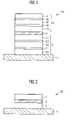
- FIG. 1shows an approach of a capacitor structure
- FIG. 2shows a further approach of a capacitor structure
- FIG. 1shows a cross-section of an approach of a capacitor structure 10 .
- a stack of a first electrode 2 , a dielectric layer 3 and a second electrode 4is arranged on a supporting substrate 1 .
- the dielectric layer 3can be chosen of high-k dielectric materials of the state of the art. These dielectric materials can comprise strontium titanate, barium strontium titanate, hafnium oxide, zirconium oxide, etc.
- the electrodes 2 , 4may have a high specific conductivity to provide a low resistance. The resistance limits the current flow to the electric capacitor and thus limits the read out time and storing time of the electric capacitor 10 .
- the first electrode 2is made of several distinct layers.
- a first layer 20consists of or comprises ruthenium.
- a second layer 21is deposited on the first layer 20 .
- the second layer 21consists of or comprises titanium nitride.
- a third layer 22is deposited on the second layer 22 .
- the third layer 22again consists of or comprises ruthenium.
- Rutheniumcan provide a high specific conductivity. A low resistivity and short delay times of the electric capacitor 10 may be achieved.
- the electric work function of rutheniummay be increased by the intermediately arranged second layer 21 comprising titanium nitride.
- a high electric work functionmay be beneficial for reducing the leakage current from the electrode 2 into the dielectric layer 3 .
- the interaction of ruthenium and titanium nitride for achieving a high electric work functionmay be enhanced by using thin first, second, and third layers 20 , 21 , 22 .
- the second layer 21has a thickness of about 1 to 10 atomic layers, at most 5 atomic layers, at most 2 atomic layers.
- the first and the third layers 20 , 22have a thickness of about 1 to 20 atomic layers, at most 10 atomic layers, at most 5 atomic layers.
- the first and third layer of ruthenium 20 , 22may be deposited by an atomic layer deposition technique or a chemical vapour deposition technique.
- the second layer 21 of titaniumis deposited by an atomic layer deposition technique or chemical vapour deposition technique, thus, its thickness may be controlled on atomic scale.
- titaniummay be deposited and transformed to titanium nitride by a subsequent thermal process in an ammonia atmosphere or plasma of nitrogen or ammonia.
- the further layerscomprise ruthenium and titanium nitride in an alternating fashion.
- the second electrode 4may be formed equal or similar to the first electrode 2 .
- the second electrode 4comprises a stack of layers 40 , 41 , 42 , 43 , 44 comprising or made of ruthenium 40 , 42 , 44 and titanium nitride 41 , 43 , respectively.
- FIG. 2illustrates a further approach of a capacitor.
- the capacitor 50comprises a first electrode 6 , a dielectric layer 3 , and a second electrode 7 .
- the first electrode 6comprises or is made of ruthenium and titanium nitride.
- the atomic ratio of ruthenium and titaniumis in the range of 0.5 to 30, for example at least 1, at least 3, at the most 10, at the most 3, about 3.
- ruthenium and titanium nitrideare forming an alloy.
- the electrode 6comprises or is made of this alloy. Most of the titanium nitride is enclosed or embedded in ruthenium. Ruthenium may not form a nitride in the alloy, but the nitrogen is chemically bound to titanium.
- the second electrode 7is formed of the same alloy as the first electrode 6 .
- the first electrode 7is deposited using a chemical vapour deposition technique; alternatively an atomic layer deposition technique may be employed.
- An exemplary deposition techniqueis described on basis of an atomic layer deposition technique.
- a first precursor transporting rutheniummay be introduced into a reaction chamber.
- a single pulse of the first precursor and removal of the hydrocarbon-group of the first precursordoes not provide a full monolayer of ruthenium. This is basically due to the larger diameter of the hydrocarbon-group compared to the lattice distance in ruthenium.
- two ruthenium atomsare most likely not deposited on neighbouring lattice points using a single pulse. Titanium nitride molecules can be deposited by a second pulse at the interstitials in the ruthenium lattice.
- the number of subsequent pulses providing rutheniumis predetermined, thus defining the number of complete monolayers made of ruthenium.
- Periodically a monolayer of rutheniumis deposited partially, only. The interstitials are filled with titanium nitride.
- the processcontinues to deposit complete monolayers of ruthenium.
- an electrodeis formed which has no complete monolayer of titanium nitride. Nevertheless, the titanium nitride is homogenously distributed in the electrode.
- Another deposition methodintroduces in parallel the first and second precursors into the reaction chamber.
- the deposition ratiois controlled by the flux of the two precursors.
- the layers 21 , 23 and electrodes 6 , 7 comprising titanium nitridemay be doped with silicon, germanium, carbon, and tin.
- An alternative approachuses iridium instead of ruthenium. It is referred to the above approach having ruthenium replaced by iridium.
- An alternative approachuses titanium oxynitride instead of titanium nitride. It is referred to the above approach having titanium nitride replaced by titanium oxynitride.
- the formation of the oxides or oxynitridesmay comprise a thermal oxidation, a remote plasma treatment, a direct plasma treatment or exposition to ozone or other oxidizing gases/plasmas.
- the deposition of metalscan be performed by electro plating, too.
- rutheniumenclose gold, silver, rhenium, platinum, palladium, rhodium and oxides of ruthenium, iridium, rhenium, and rhodium.
- titanium nitrideenclose tantalum nitride, tantalum oxynitride, tungsten nitride, tungsten oxynitride, molybdenum nitride, molybdenum oxynitride, vanadium nitride, vanadium oxynitride, niobium nitride, niobium oxynitride, nickel oxynitride, strontium oxide, strontium oxynitride, barium oxide, barium oxynitride, cobalt oxynitride.
- tin oxide, zinc oxidemay be used.
- the capacitorcan be formed as stack capacitor or deep trench capacitor.
Landscapes
- Semiconductor Memories (AREA)
Abstract
Description
- 1. Field of the Invention
- The present invention generally relates to an electrode of an integrated circuit.
- 2. Description of the Related Art
- Although in principle applicable to arbitrary integrated semiconductor structures, the following technology and the underlying problems will be explained with respect to a capacitor electrode.
- In recent years, lateral dimensions of electric capacitors have been reduced steadily. Electric capacity of the capacitors is maintained by increasing the vertical extension. Further, high-k dielectric materials are used as capacitor dielectrics.
- A further important property of electric capacitors is the retention time of an electric charge in the electric capacitor. The retention time is limited by leakage currents between the electrodes or into the dielectric material. Due to the short distance between the electrodes and the medium isolation properties of high-k dielectric materials, like barium strontium titanate (BST), hafnium oxide etc., leakage currents are becoming an important issue.
- According to an aspect of the technology, an electrode of an integrated circuit comprises: at least one metallic layer comprising a first metallic material selected of at least one of ruthenium, ruthenium oxide, iridium, iridium oxide, platinum, palladium, gold, silver, rhenium, and rhodium and a metal compound selected of a nitride, an oxide, and an oxynitride of a second metallic material. The second compound is embedded by the at least one metallic layer.
- According to a further aspect of the technology an electrode of an integrated circuit comprises a multilayer stack of at least two first layers and at least one second layer, which are arranged alternatingly. The first layers comprise of at least one of ruthenium, ruthenium oxide, iridium, iridium oxide, platinum, palladium, gold, silver, rhenium, and rhodium. The second layer comprises a compound selected of a nitride, an oxide, and an oxynitride of a second metallic material selected of the group of the second the fourth, the fifth, and the sixth group of the periodic table.
- According to a further aspect of the technology an electrode of an integrated circuit comprises at least one metallic layer comprising a first metallic material selected of at least one of ruthenium, ruthenium oxide, iridium, iridium oxide, platinum, palladium, gold, silver, rhenium, and rhodium and a metal compound selected of a nitride, an oxide, and an oxynitride of a second metallic material selected of the group of the second, the fourth, the fifth, and the sixth group of the periodic table. The metal compound is arranged as implant in the at least one metallic layer.
- According to a further aspect an electrode of an integrated circuit comprises at least one metal oxide layer comprising an oxide of a first metallic material selected of at least one of ruthenium, iridium, rhenium, and rhodium and a metal compound selected of a nitride, an oxide, and an oxynitride of a second metallic material. The second compound is embedded by the at least one metallic layer.
- In the following description, reference is made to the accompanying drawings that form part hereof, and in which is shown by way of illustration one or more specific implementations in which the invention may be practiced. It is to be understood that other implementations may be utilized and structural changes may be made without departing from the scope of this invention.
FIG. 1 shows an approach of a capacitor structureFIG. 2 shows a further approach of a capacitor structure- The invention can be better understood by referring to the following figures. The components in the figures are not necessarily to scale, emphasis instead being placed upon illustrating the principles of the invention. In the figures, like reference numerals designate corresponding parts throughout the different views.
- It is to be understood and appreciated that the process steps and structures described below do not form a complete process flow for the manufacture of integrated circuits. The present technology can be practiced in conjunction with integrated circuit fabrication techniques that are currently used in the art, and only so much of the commonly practiced process steps are included herein as are necessary to provide an understanding of the present technology.
FIG. 1 shows a cross-section of an approach of acapacitor structure 10. On a supporting substrate1, a stack of afirst electrode 2, adielectric layer 3 and asecond electrode 4 is arranged.- The
dielectric layer 3 can be chosen of high-k dielectric materials of the state of the art. These dielectric materials can comprise strontium titanate, barium strontium titanate, hafnium oxide, zirconium oxide, etc. - The
electrodes electric capacitor 10. - The
first electrode 2 is made of several distinct layers. Afirst layer 20 consists of or comprises ruthenium. Asecond layer 21 is deposited on thefirst layer 20. Thesecond layer 21 consists of or comprises titanium nitride. Athird layer 22 is deposited on thesecond layer 22. Thethird layer 22 again consists of or comprises ruthenium. - Ruthenium can provide a high specific conductivity. A low resistivity and short delay times of the
electric capacitor 10 may be achieved. - The electric work function of ruthenium may be increased by the intermediately arranged
second layer 21 comprising titanium nitride. A high electric work function may be beneficial for reducing the leakage current from theelectrode 2 into thedielectric layer 3. - The interaction of ruthenium and titanium nitride for achieving a high electric work function may be enhanced by using thin first, second, and
third layers - The
second layer 21 has a thickness of about 1 to 10 atomic layers, at most 5 atomic layers, at most 2 atomic layers. The first and thethird layers - The first and third layer of
ruthenium second layer 21 of titanium is deposited by an atomic layer deposition technique or chemical vapour deposition technique, thus, its thickness may be controlled on atomic scale. Alternatively, titanium may be deposited and transformed to titanium nitride by a subsequent thermal process in an ammonia atmosphere or plasma of nitrogen or ammonia. - On the above stack of three
layers further layers - The
second electrode 4 may be formed equal or similar to thefirst electrode 2. Thesecond electrode 4 comprises a stack oflayers ruthenium titanium nitride FIG. 2 illustrates a further approach of a capacitor. Thecapacitor 50 comprises a first electrode6, adielectric layer 3, and a second electrode7.- The first electrode6 comprises or is made of ruthenium and titanium nitride. The atomic ratio of ruthenium and titanium is in the range of 0.5 to 30, for example at least 1, at least 3, at the most 10, at the most 3, about 3.
- In this approach ruthenium and titanium nitride are forming an alloy. The electrode6 comprises or is made of this alloy. Most of the titanium nitride is enclosed or embedded in ruthenium. Ruthenium may not form a nitride in the alloy, but the nitrogen is chemically bound to titanium.
- The second electrode7 is formed of the same alloy as the first electrode6.
- The first electrode7 is deposited using a chemical vapour deposition technique; alternatively an atomic layer deposition technique may be employed.
- An exemplary deposition technique is described on basis of an atomic layer deposition technique. A first precursor transporting ruthenium may be introduced into a reaction chamber. A single pulse of the first precursor and removal of the hydrocarbon-group of the first precursor does not provide a full monolayer of ruthenium. This is basically due to the larger diameter of the hydrocarbon-group compared to the lattice distance in ruthenium. Thus, two ruthenium atoms are most likely not deposited on neighbouring lattice points using a single pulse. Titanium nitride molecules can be deposited by a second pulse at the interstitials in the ruthenium lattice. The number of subsequent pulses providing ruthenium is predetermined, thus defining the number of complete monolayers made of ruthenium. Periodically a monolayer of ruthenium is deposited partially, only. The interstitials are filled with titanium nitride. The process continues to deposit complete monolayers of ruthenium. Thus, an electrode is formed which has no complete monolayer of titanium nitride. Nevertheless, the titanium nitride is homogenously distributed in the electrode.
- Another deposition method introduces in parallel the first and second precursors into the reaction chamber. The deposition ratio is controlled by the flux of the two precursors.
- The
layers - An alternative approach uses iridium instead of ruthenium. It is referred to the above approach having ruthenium replaced by iridium.
- An alternative approach uses titanium oxynitride instead of titanium nitride. It is referred to the above approach having titanium nitride replaced by titanium oxynitride.
- The formation of the oxides or oxynitrides may comprise a thermal oxidation, a remote plasma treatment, a direct plasma treatment or exposition to ozone or other oxidizing gases/plasmas.
- The deposition of metals can be performed by electro plating, too.
- Other materials suitable as substitute for ruthenium enclose gold, silver, rhenium, platinum, palladium, rhodium and oxides of ruthenium, iridium, rhenium, and rhodium.
- Other materials suitable as substitute for titanium nitride enclose tantalum nitride, tantalum oxynitride, tungsten nitride, tungsten oxynitride, molybdenum nitride, molybdenum oxynitride, vanadium nitride, vanadium oxynitride, niobium nitride, niobium oxynitride, nickel oxynitride, strontium oxide, strontium oxynitride, barium oxide, barium oxynitride, cobalt oxynitride. Alternatively, tin oxide, zinc oxide may be used.
- The capacitor can be formed as stack capacitor or deep trench capacitor.
- Other systems, methods features and advantages of the invention will be or will become apparent to one with skill in the art upon examination of the following figures and detailed description. It is intended that all such additional systems, methods, features and advantages be included within this description, be within the scope of the invention, and be protected by the accompanying claims.
Claims (17)
Priority Applications (1)
| Application Number | Priority Date | Filing Date | Title |
|---|---|---|---|
| US12/023,321US8344438B2 (en) | 2008-01-31 | 2008-01-31 | Electrode of an integrated circuit |
Applications Claiming Priority (1)
| Application Number | Priority Date | Filing Date | Title |
|---|---|---|---|
| US12/023,321US8344438B2 (en) | 2008-01-31 | 2008-01-31 | Electrode of an integrated circuit |
Publications (2)
| Publication Number | Publication Date |
|---|---|
| US20090194410A1true US20090194410A1 (en) | 2009-08-06 |
| US8344438B2 US8344438B2 (en) | 2013-01-01 |
Family
ID=40930596
Family Applications (1)
| Application Number | Title | Priority Date | Filing Date |
|---|---|---|---|
| US12/023,321Expired - Fee RelatedUS8344438B2 (en) | 2008-01-31 | 2008-01-31 | Electrode of an integrated circuit |
Country Status (1)
| Country | Link |
|---|---|
| US (1) | US8344438B2 (en) |
Cited By (2)
| Publication number | Priority date | Publication date | Assignee | Title |
|---|---|---|---|---|
| US9466660B2 (en) | 2013-10-16 | 2016-10-11 | Micron Technology, Inc. | Semiconductor structures including molybdenum nitride, molybdenum oxynitride or molybdenum-based alloy material, and method of making such structures |
| US9929405B2 (en)* | 2010-04-12 | 2018-03-27 | Belenos Clean Power Holding Ag | Electrode comprising a transition metal oxidenitride or a nitrogen-doped transition metal oxide as electronically active material |
Families Citing this family (3)
| Publication number | Priority date | Publication date | Assignee | Title |
|---|---|---|---|---|
| US8809827B1 (en)* | 2013-03-13 | 2014-08-19 | International Business Machines Corporation | Thermally assisted MRAM with multilayer strap and top contact for low thermal conductivity |
| US9515251B2 (en) | 2014-04-09 | 2016-12-06 | International Business Machines Corporation | Structure for thermally assisted MRAM |
| US12046658B2 (en)* | 2019-07-11 | 2024-07-23 | Micron Technology, Inc. | Electrode formation |
Citations (27)
| Publication number | Priority date | Publication date | Assignee | Title |
|---|---|---|---|---|
| US5005102A (en)* | 1989-06-20 | 1991-04-02 | Ramtron Corporation | Multilayer electrodes for integrated circuit capacitors |
| US5262920A (en)* | 1991-05-16 | 1993-11-16 | Nec Corporation | Thin film capacitor |
| US5520992A (en)* | 1992-04-20 | 1996-05-28 | Texas Instruments Incorporated | Electrodes for high dielectric constant materials |
| US5612574A (en)* | 1995-06-06 | 1997-03-18 | Texas Instruments Incorporated | Semiconductor structures using high-dielectric-constant materials and an adhesion layer |
| US5790366A (en)* | 1996-12-06 | 1998-08-04 | Sharp Kabushiki Kaisha | High temperature electrode-barriers for ferroelectric and other capacitor structures |
| US6291889B1 (en)* | 1995-04-12 | 2001-09-18 | Northrop Grumman Corporation | High temperature resistant thin-film system |
| US20020086164A1 (en)* | 1999-04-06 | 2002-07-04 | Nippon Sheet Glass Co., Ltd. | Light transmitting electromagnetic wave filter and process for producing the same |
| US20020184939A1 (en)* | 1997-10-10 | 2002-12-12 | Tapesh Yadav | Multilaminated nano-engineered devices |
| US6525358B2 (en)* | 1999-01-12 | 2003-02-25 | Agere Systems Inc. | Capacitor having the lower electrode for preventing undesired defects at the surface of the metal plug |
| US6617634B2 (en)* | 2000-08-30 | 2003-09-09 | Micron Technology, Inc. | RuSixOy-containing adhesion layers and process for fabricating the same |
| US6670233B2 (en)* | 2001-05-30 | 2003-12-30 | International Business Machines Corporation | Methods of patterning a multi-layer film stack and forming a lower electrode of a capacitor |
| US20040070017A1 (en)* | 2000-01-18 | 2004-04-15 | Micron Technology, Inc. | Metal oxynitride capacitor barrier layer |
| US20040090500A1 (en)* | 2001-09-28 | 2004-05-13 | Seiko Epson Corporation | Piezoelectric thin film element, manufacturing method thereof, and liquid ejecting head and liquid ejecting apparatus employing same |
| US20040101709A1 (en)* | 2002-11-27 | 2004-05-27 | Guocun Chen | Coated article |
| US20040166672A1 (en)* | 1997-12-12 | 2004-08-26 | Reinberg Alan R. | Oxidative conditioning compositions for metal oxide layer and applications thereof |
| US20040173823A1 (en)* | 1998-10-14 | 2004-09-09 | Masami Murai | Method for manufacturing ferroelectric thin film device, ink jet recording head and ink jet printer |
| US20040179259A1 (en)* | 2003-03-11 | 2004-09-16 | Fuji Photo Film Co., Ltd. | Display device |
| US20050101085A1 (en)* | 2002-03-28 | 2005-05-12 | Matsushita Electric Industrial Co., Ltd. | Semiconductor device and method for fabricating the same |
| US20050145970A1 (en)* | 2002-01-04 | 2005-07-07 | Rutgers, The State University Of New Jersey | Schottky diode with silver layer contacting the ZnO and MgxZn1-xO films |
| US20050145916A1 (en)* | 2003-12-15 | 2005-07-07 | Samsung Electronics Co., Ltd. | Capacitor of a semiconductor device and manufacturing method thereof |
| US20050157544A1 (en)* | 2004-01-20 | 2005-07-21 | Headway Technologies, Inc. | Magnetic tunneling junction film structure with process determined in-plane magnetic anisotropy |
| US20050260823A9 (en)* | 1998-08-26 | 2005-11-24 | Micron Technology, Inc. | Methods and apparatus for forming rhodium-containing layers |
| US7026680B2 (en)* | 2003-03-12 | 2006-04-11 | Fujitsu Limited | Thin film capacitive element, method for producing same and electronic device |
| US20060124983A1 (en)* | 2003-10-22 | 2006-06-15 | Matsushita Electric Industrial Co., Ltd. | Semiconductor device and method for fabricating the same |
| US20070059502A1 (en)* | 2005-05-05 | 2007-03-15 | Applied Materials, Inc. | Integrated process for sputter deposition of a conductive barrier layer, especially an alloy of ruthenium and tantalum, underlying copper or copper alloy seed layer |
| US20070097651A1 (en)* | 2005-11-01 | 2007-05-03 | Techfilm, Llc | Thermal interface material with multiple size distribution thermally conductive fillers |
| US20070263340A1 (en)* | 1999-03-01 | 2007-11-15 | Micron Technology, Inc. | Thin film structure that may be used with an adhesion layer |
- 2008
- 2008-01-31USUS12/023,321patent/US8344438B2/ennot_activeExpired - Fee Related
Patent Citations (27)
| Publication number | Priority date | Publication date | Assignee | Title |
|---|---|---|---|---|
| US5005102A (en)* | 1989-06-20 | 1991-04-02 | Ramtron Corporation | Multilayer electrodes for integrated circuit capacitors |
| US5262920A (en)* | 1991-05-16 | 1993-11-16 | Nec Corporation | Thin film capacitor |
| US5520992A (en)* | 1992-04-20 | 1996-05-28 | Texas Instruments Incorporated | Electrodes for high dielectric constant materials |
| US6291889B1 (en)* | 1995-04-12 | 2001-09-18 | Northrop Grumman Corporation | High temperature resistant thin-film system |
| US5612574A (en)* | 1995-06-06 | 1997-03-18 | Texas Instruments Incorporated | Semiconductor structures using high-dielectric-constant materials and an adhesion layer |
| US5790366A (en)* | 1996-12-06 | 1998-08-04 | Sharp Kabushiki Kaisha | High temperature electrode-barriers for ferroelectric and other capacitor structures |
| US20020184939A1 (en)* | 1997-10-10 | 2002-12-12 | Tapesh Yadav | Multilaminated nano-engineered devices |
| US20040166672A1 (en)* | 1997-12-12 | 2004-08-26 | Reinberg Alan R. | Oxidative conditioning compositions for metal oxide layer and applications thereof |
| US20050260823A9 (en)* | 1998-08-26 | 2005-11-24 | Micron Technology, Inc. | Methods and apparatus for forming rhodium-containing layers |
| US20040173823A1 (en)* | 1998-10-14 | 2004-09-09 | Masami Murai | Method for manufacturing ferroelectric thin film device, ink jet recording head and ink jet printer |
| US6525358B2 (en)* | 1999-01-12 | 2003-02-25 | Agere Systems Inc. | Capacitor having the lower electrode for preventing undesired defects at the surface of the metal plug |
| US20070263340A1 (en)* | 1999-03-01 | 2007-11-15 | Micron Technology, Inc. | Thin film structure that may be used with an adhesion layer |
| US20020086164A1 (en)* | 1999-04-06 | 2002-07-04 | Nippon Sheet Glass Co., Ltd. | Light transmitting electromagnetic wave filter and process for producing the same |
| US20040070017A1 (en)* | 2000-01-18 | 2004-04-15 | Micron Technology, Inc. | Metal oxynitride capacitor barrier layer |
| US6617634B2 (en)* | 2000-08-30 | 2003-09-09 | Micron Technology, Inc. | RuSixOy-containing adhesion layers and process for fabricating the same |
| US6670233B2 (en)* | 2001-05-30 | 2003-12-30 | International Business Machines Corporation | Methods of patterning a multi-layer film stack and forming a lower electrode of a capacitor |
| US20040090500A1 (en)* | 2001-09-28 | 2004-05-13 | Seiko Epson Corporation | Piezoelectric thin film element, manufacturing method thereof, and liquid ejecting head and liquid ejecting apparatus employing same |
| US20050145970A1 (en)* | 2002-01-04 | 2005-07-07 | Rutgers, The State University Of New Jersey | Schottky diode with silver layer contacting the ZnO and MgxZn1-xO films |
| US20050101085A1 (en)* | 2002-03-28 | 2005-05-12 | Matsushita Electric Industrial Co., Ltd. | Semiconductor device and method for fabricating the same |
| US20040101709A1 (en)* | 2002-11-27 | 2004-05-27 | Guocun Chen | Coated article |
| US20040179259A1 (en)* | 2003-03-11 | 2004-09-16 | Fuji Photo Film Co., Ltd. | Display device |
| US7026680B2 (en)* | 2003-03-12 | 2006-04-11 | Fujitsu Limited | Thin film capacitive element, method for producing same and electronic device |
| US20060124983A1 (en)* | 2003-10-22 | 2006-06-15 | Matsushita Electric Industrial Co., Ltd. | Semiconductor device and method for fabricating the same |
| US20050145916A1 (en)* | 2003-12-15 | 2005-07-07 | Samsung Electronics Co., Ltd. | Capacitor of a semiconductor device and manufacturing method thereof |
| US20050157544A1 (en)* | 2004-01-20 | 2005-07-21 | Headway Technologies, Inc. | Magnetic tunneling junction film structure with process determined in-plane magnetic anisotropy |
| US20070059502A1 (en)* | 2005-05-05 | 2007-03-15 | Applied Materials, Inc. | Integrated process for sputter deposition of a conductive barrier layer, especially an alloy of ruthenium and tantalum, underlying copper or copper alloy seed layer |
| US20070097651A1 (en)* | 2005-11-01 | 2007-05-03 | Techfilm, Llc | Thermal interface material with multiple size distribution thermally conductive fillers |
Cited By (2)
| Publication number | Priority date | Publication date | Assignee | Title |
|---|---|---|---|---|
| US9929405B2 (en)* | 2010-04-12 | 2018-03-27 | Belenos Clean Power Holding Ag | Electrode comprising a transition metal oxidenitride or a nitrogen-doped transition metal oxide as electronically active material |
| US9466660B2 (en) | 2013-10-16 | 2016-10-11 | Micron Technology, Inc. | Semiconductor structures including molybdenum nitride, molybdenum oxynitride or molybdenum-based alloy material, and method of making such structures |
Also Published As
| Publication number | Publication date |
|---|---|
| US8344438B2 (en) | 2013-01-01 |
Similar Documents
| Publication | Publication Date | Title |
|---|---|---|
| US8574983B2 (en) | Method for fabricating a DRAM capacitor having increased thermal and chemical stability | |
| US8542523B2 (en) | Method for fabricating a DRAM capacitor having increased thermal and chemical stability | |
| KR20180116321A (en) | A barrier layer for a correlated electronic material | |
| JP4814781B2 (en) | Dielectric film forming method, capacitor using the dielectric film, and manufacturing method thereof | |
| KR101632496B1 (en) | Energy storage capacitor, method of fabricating the same, and power electronics having the same | |
| US8861179B2 (en) | Capacitors having dielectric regions that include multiple metal oxide-comprising materials | |
| KR20090038924A (en) | Zirconium Substituted Barium Titanate Gate Dielectric | |
| US9159551B2 (en) | Methods of forming capacitors | |
| JP6101068B2 (en) | Metal-insulator-metal stack and manufacturing method thereof | |
| JP2008258623A (en) | Zirconium oxide capacitor and method of manufacturing the same | |
| JP2008028249A (en) | Semiconductor device and manufacturing method of semiconductor device | |
| US8344438B2 (en) | Electrode of an integrated circuit | |
| KR20090000431A (en) | CAPACITOR WITH RUTHENIUM-BASED ELECTRODE AND METHOD FOR MANUFACTURING THE SAME | |
| US12062689B2 (en) | Manufacturing method of capacitor structure | |
| KR100568516B1 (en) | How to manufacture analog capacitors using post-processing technology | |
| EP1770725A2 (en) | Dielectric film production process and capacitor | |
| CN112714945A (en) | Method for manufacturing semiconductor device | |
| US8202808B2 (en) | Methods of forming strontium titanate films | |
| KR20210002833A (en) | Method of manufacturing electrode layer and method of manufacturing capacitor using the same | |
| US9099430B2 (en) | ZrO-based high K dielectric stack for logic decoupling capacitor or embedded DRAM | |
| WO2007046628A2 (en) | Insulator undergoing abrupt metal-insulator transition, method of manufacturing the insulator, and device using the insulator | |
| KR100716642B1 (en) | Capacitor dielectric film and manufacturing method thereof | |
| Tsui et al. | High-Performance Metal–Insulator–Metal Capacitors With $\hbox {HfTiO}/\hbox {Y} _ {2}\hbox {O} _ {3} $ Stacked Dielectric | |
| US20150318108A1 (en) | IN-SITU OXIDIZED NiO AS ELECTRODE SURFACE FOR HIGH k MIM DEVICE | |
| Ahn et al. | Effect of Sr–Ruthenate Seed Layer on Dielectric Properties of SrTiO3 Thin Films Prepared by Plasma-Enhanced Atomic Layer Deposition |
Legal Events
| Date | Code | Title | Description |
|---|---|---|---|
| AS | Assignment | Owner name:QIMONDA AG, GERMANY Free format text:ASSIGNMENT OF ASSIGNORS INTEREST;ASSIGNORS:SCHROEDER, UWE;JAKSCHIK, STEFAN;HEITMANN, JOHANNES;AND OTHERS;REEL/FRAME:020526/0775;SIGNING DATES FROM 20080211 TO 20080213 Owner name:QIMONDA AG, GERMANY Free format text:ASSIGNMENT OF ASSIGNORS INTEREST;ASSIGNORS:SCHROEDER, UWE;JAKSCHIK, STEFAN;HEITMANN, JOHANNES;AND OTHERS;SIGNING DATES FROM 20080211 TO 20080213;REEL/FRAME:020526/0775 | |
| FEPP | Fee payment procedure | Free format text:PAYOR NUMBER ASSIGNED (ORIGINAL EVENT CODE: ASPN); ENTITY STATUS OF PATENT OWNER: LARGE ENTITY | |
| STCF | Information on status: patent grant | Free format text:PATENTED CASE | |
| AS | Assignment | Owner name:INFINEON TECHNOLOGIES AG, GERMANY Free format text:ASSIGNMENT OF ASSIGNORS INTEREST;ASSIGNOR:QIMONDA AG;REEL/FRAME:035623/0001 Effective date:20141009 | |
| AS | Assignment | Owner name:POLARIS INNOVATIONS LIMITED, IRELAND Free format text:ASSIGNMENT OF ASSIGNORS INTEREST;ASSIGNOR:INFINEON TECHNOLOGIES AG;REEL/FRAME:036575/0670 Effective date:20150708 | |
| FPAY | Fee payment | Year of fee payment:4 | |
| FEPP | Fee payment procedure | Free format text:MAINTENANCE FEE REMINDER MAILED (ORIGINAL EVENT CODE: REM.); ENTITY STATUS OF PATENT OWNER: LARGE ENTITY | |
| LAPS | Lapse for failure to pay maintenance fees | Free format text:PATENT EXPIRED FOR FAILURE TO PAY MAINTENANCE FEES (ORIGINAL EVENT CODE: EXP.); ENTITY STATUS OF PATENT OWNER: LARGE ENTITY | |
| STCH | Information on status: patent discontinuation | Free format text:PATENT EXPIRED DUE TO NONPAYMENT OF MAINTENANCE FEES UNDER 37 CFR 1.362 | |
| FP | Lapsed due to failure to pay maintenance fee | Effective date:20210101 |