US20090194162A1 - Method to form a photovoltaic cell comprising a thin lamina - Google Patents
Method to form a photovoltaic cell comprising a thin laminaDownload PDFInfo
- Publication number
- US20090194162A1 US20090194162A1US12/026,530US2653008AUS2009194162A1US 20090194162 A1US20090194162 A1US 20090194162A1US 2653008 AUS2653008 AUS 2653008AUS 2009194162 A1US2009194162 A1US 2009194162A1
- Authority
- US
- United States
- Prior art keywords
- lamina
- photovoltaic cell
- semiconductor
- thickness
- ions
- Prior art date
- Legal status (The legal status is an assumption and is not a legal conclusion. Google has not performed a legal analysis and makes no representation as to the accuracy of the status listed.)
- Granted
Links
- 238000000034methodMethods0.000titleclaimsdescription89
- 239000004065semiconductorSubstances0.000claimsabstractdescription100
- 150000002500ionsChemical class0.000claimsabstractdescription66
- 238000005468ion implantationMethods0.000claimsabstractdescription9
- 229910052710siliconInorganic materials0.000claimsdescription48
- 239000010703siliconSubstances0.000claimsdescription48
- XUIMIQQOPSSXEZ-UHFFFAOYSA-NSiliconChemical compound[Si]XUIMIQQOPSSXEZ-UHFFFAOYSA-N0.000claimsdescription47
- 239000007943implantSubstances0.000claimsdescription45
- 239000001257hydrogenSubstances0.000claimsdescription42
- 229910052739hydrogenInorganic materials0.000claimsdescription42
- 239000000758substrateSubstances0.000claimsdescription42
- 239000000463materialSubstances0.000claimsdescription40
- 239000007789gasSubstances0.000claimsdescription32
- UFHFLCQGNIYNRP-UHFFFAOYSA-NHydrogenChemical compound[H][H]UFHFLCQGNIYNRP-UHFFFAOYSA-N0.000claimsdescription28
- 229910052751metalInorganic materials0.000claimsdescription23
- 239000002184metalSubstances0.000claimsdescription23
- 239000001307heliumSubstances0.000claimsdescription19
- 229910052734heliumInorganic materials0.000claimsdescription19
- -1hydrogen ionsChemical class0.000claimsdescription19
- 238000000151depositionMethods0.000claimsdescription12
- 239000011521glassSubstances0.000claimsdescription6
- 229910052796boronInorganic materials0.000claimsdescription5
- 239000013078crystalSubstances0.000claimsdescription5
- 229920000642polymerPolymers0.000claimsdescription5
- GNPVGFCGXDBREM-UHFFFAOYSA-Ngermanium atomChemical compound[Ge]GNPVGFCGXDBREM-UHFFFAOYSA-N0.000claimsdescription4
- 239000011800void materialSubstances0.000claims1
- 235000012431wafersNutrition0.000description106
- 238000004299exfoliationMethods0.000description28
- 238000009792diffusion processMethods0.000description27
- 229910052782aluminiumInorganic materials0.000description24
- XAGFODPZIPBFFR-UHFFFAOYSA-NaluminiumChemical compound[Al]XAGFODPZIPBFFR-UHFFFAOYSA-N0.000description24
- 229910052581Si3N4Inorganic materials0.000description19
- HQVNEWCFYHHQES-UHFFFAOYSA-Nsilicon nitrideChemical compoundN12[Si]34N5[Si]62N3[Si]51N64HQVNEWCFYHHQES-UHFFFAOYSA-N0.000description19
- 230000015572biosynthetic processEffects0.000description17
- 125000004429atomChemical group0.000description16
- VYPSYNLAJGMNEJ-UHFFFAOYSA-NSilicium dioxideChemical compoundO=[Si]=OVYPSYNLAJGMNEJ-UHFFFAOYSA-N0.000description14
- 238000009826distributionMethods0.000description14
- SWQJXJOGLNCZEY-UHFFFAOYSA-Nhelium atomChemical compound[He]SWQJXJOGLNCZEY-UHFFFAOYSA-N0.000description14
- 230000003667anti-reflective effectEffects0.000description13
- 230000008569processEffects0.000description13
- 230000003746surface roughnessEffects0.000description13
- 239000002019doping agentSubstances0.000description12
- 230000007547defectEffects0.000description10
- 229910021421monocrystalline siliconInorganic materials0.000description9
- 238000004519manufacturing processMethods0.000description8
- 238000006243chemical reactionMethods0.000description7
- 238000005530etchingMethods0.000description7
- 238000002513implantationMethods0.000description7
- 239000000377silicon dioxideSubstances0.000description7
- 229910021417amorphous siliconInorganic materials0.000description6
- 230000008021depositionEffects0.000description6
- 150000002431hydrogenChemical class0.000description6
- 235000012239silicon dioxideNutrition0.000description6
- 239000010408filmSubstances0.000description5
- 229910021420polycrystalline siliconInorganic materials0.000description5
- XLOMVQKBTHCTTD-UHFFFAOYSA-NZinc monoxideChemical compound[Zn]=OXLOMVQKBTHCTTD-UHFFFAOYSA-N0.000description4
- 238000004458analytical methodMethods0.000description4
- QVGXLLKOCUKJST-UHFFFAOYSA-Natomic oxygenChemical compound[O]QVGXLLKOCUKJST-UHFFFAOYSA-N0.000description4
- 230000003247decreasing effectEffects0.000description4
- 230000001965increasing effectEffects0.000description4
- 239000001301oxygenSubstances0.000description4
- 229910052760oxygenInorganic materials0.000description4
- 238000000059patterningMethods0.000description4
- 238000000623plasma-assisted chemical vapour depositionMethods0.000description4
- 238000007650screen-printingMethods0.000description4
- 238000000926separation methodMethods0.000description4
- ZOXJGFHDIHLPTG-UHFFFAOYSA-NBoronChemical compound[B]ZOXJGFHDIHLPTG-UHFFFAOYSA-N0.000description3
- 229910001218Gallium arsenideInorganic materials0.000description3
- BQCADISMDOOEFD-UHFFFAOYSA-NSilverChemical compound[Ag]BQCADISMDOOEFD-UHFFFAOYSA-N0.000description3
- 230000004888barrier functionEffects0.000description3
- 229910052732germaniumInorganic materials0.000description3
- 125000004435hydrogen atomChemical group[H]*0.000description3
- 230000000873masking effectEffects0.000description3
- 229910021424microcrystalline siliconInorganic materials0.000description3
- 230000005855radiationEffects0.000description3
- 229910052709silverInorganic materials0.000description3
- 239000004332silverSubstances0.000description3
- XKRFYHLGVUSROY-UHFFFAOYSA-NArgonChemical compound[Ar]XKRFYHLGVUSROY-UHFFFAOYSA-N0.000description2
- YZCKVEUIGOORGS-UHFFFAOYSA-NHydrogen atomChemical compound[H]YZCKVEUIGOORGS-UHFFFAOYSA-N0.000description2
- 229910000577Silicon-germaniumInorganic materials0.000description2
- GWEVSGVZZGPLCZ-UHFFFAOYSA-NTitan oxideChemical compoundO=[Ti]=OGWEVSGVZZGPLCZ-UHFFFAOYSA-N0.000description2
- RTAQQCXQSZGOHL-UHFFFAOYSA-NTitaniumChemical compound[Ti]RTAQQCXQSZGOHL-UHFFFAOYSA-N0.000description2
- LEVVHYCKPQWKOP-UHFFFAOYSA-N[Si].[Ge]Chemical compound[Si].[Ge]LEVVHYCKPQWKOP-UHFFFAOYSA-N0.000description2
- 230000003190augmentative effectEffects0.000description2
- 238000005452bendingMethods0.000description2
- 229910021419crystalline siliconInorganic materials0.000description2
- 238000005520cutting processMethods0.000description2
- 230000007423decreaseEffects0.000description2
- 238000006073displacement reactionMethods0.000description2
- 230000000694effectsEffects0.000description2
- 230000005684electric fieldEffects0.000description2
- 238000005516engineering processMethods0.000description2
- AMGQUBHHOARCQH-UHFFFAOYSA-Nindium;oxotinChemical compound[In].[Sn]=OAMGQUBHHOARCQH-UHFFFAOYSA-N0.000description2
- 239000012212insulatorSubstances0.000description2
- 230000003993interactionEffects0.000description2
- 239000007769metal materialSubstances0.000description2
- XHXFXVLFKHQFAL-UHFFFAOYSA-Nphosphoryl trichlorideChemical compoundClP(Cl)(Cl)=OXHXFXVLFKHQFAL-UHFFFAOYSA-N0.000description2
- 238000000206photolithographyMethods0.000description2
- 230000006798recombinationEffects0.000description2
- 238000005215recombinationMethods0.000description2
- 238000005476solderingMethods0.000description2
- 239000007787solidSubstances0.000description2
- 239000010936titaniumSubstances0.000description2
- 229910052719titaniumInorganic materials0.000description2
- OGIDPMRJRNCKJF-UHFFFAOYSA-Ntitanium oxideInorganic materials[Ti]=OOGIDPMRJRNCKJF-UHFFFAOYSA-N0.000description2
- 239000011787zinc oxideSubstances0.000description2
- AANMVENRNJYEMK-UHFFFAOYSA-N4-propan-2-ylcyclohex-2-en-1-oneChemical compoundCC(C)C1CCC(=O)C=C1AANMVENRNJYEMK-UHFFFAOYSA-N0.000description1
- JBRZTFJDHDCESZ-UHFFFAOYSA-NAsGaChemical compound[As]#[Ga]JBRZTFJDHDCESZ-UHFFFAOYSA-N0.000description1
- 229910015844BCl3Inorganic materials0.000description1
- 229910004613CdTeInorganic materials0.000description1
- VYZAMTAEIAYCRO-UHFFFAOYSA-NChromiumChemical compound[Cr]VYZAMTAEIAYCRO-UHFFFAOYSA-N0.000description1
- YZCKVEUIGOORGS-OUBTZVSYSA-NDeuteriumChemical compound[2H]YZCKVEUIGOORGS-OUBTZVSYSA-N0.000description1
- ZOKXTWBITQBERF-UHFFFAOYSA-NMolybdenumChemical compound[Mo]ZOKXTWBITQBERF-UHFFFAOYSA-N0.000description1
- 229910019213POCl3Inorganic materials0.000description1
- QCWXUUIWCKQGHC-UHFFFAOYSA-NZirconiumChemical compound[Zr]QCWXUUIWCKQGHC-UHFFFAOYSA-N0.000description1
- 238000010521absorption reactionMethods0.000description1
- 238000000137annealingMethods0.000description1
- 230000003466anti-cipated effectEffects0.000description1
- 239000006117anti-reflective coatingSubstances0.000description1
- 229910052786argonInorganic materials0.000description1
- 230000008901benefitEffects0.000description1
- 229910001423beryllium ionInorganic materials0.000description1
- 239000005388borosilicate glassSubstances0.000description1
- 239000000969carrierSubstances0.000description1
- 229910052804chromiumInorganic materials0.000description1
- 239000011651chromiumSubstances0.000description1
- 238000004140cleaningMethods0.000description1
- 238000003776cleavage reactionMethods0.000description1
- 239000011248coating agentSubstances0.000description1
- 238000000576coating methodMethods0.000description1
- 229910052681coesiteInorganic materials0.000description1
- 150000001875compoundsChemical class0.000description1
- 239000004020conductorSubstances0.000description1
- 238000007796conventional methodMethods0.000description1
- 229910052906cristobaliteInorganic materials0.000description1
- 229910052805deuteriumInorganic materials0.000description1
- 230000008020evaporationEffects0.000description1
- 238000001704evaporationMethods0.000description1
- 238000010304firingMethods0.000description1
- 230000004907fluxEffects0.000description1
- 238000010438heat treatmentMethods0.000description1
- 238000005984hydrogenation reactionMethods0.000description1
- 239000012535impuritySubstances0.000description1
- 230000001939inductive effectEffects0.000description1
- 239000011810insulating materialSubstances0.000description1
- 230000031700light absorptionEffects0.000description1
- 239000011159matrix materialSubstances0.000description1
- 239000013081microcrystalSubstances0.000description1
- 229910052750molybdenumInorganic materials0.000description1
- 239000011733molybdenumSubstances0.000description1
- 229910052754neonInorganic materials0.000description1
- GKAOGPIIYCISHV-UHFFFAOYSA-Nneon atomChemical compound[Ne]GKAOGPIIYCISHV-UHFFFAOYSA-N0.000description1
- 239000002245particleSubstances0.000description1
- 230000000737periodic effectEffects0.000description1
- 229910021426porous siliconInorganic materials0.000description1
- 230000007017scissionEffects0.000description1
- 238000004544sputter depositionMethods0.000description1
- 229910052682stishoviteInorganic materials0.000description1
- 229910052715tantalumInorganic materials0.000description1
- GUVRBAGPIYLISA-UHFFFAOYSA-Ntantalum atomChemical compound[Ta]GUVRBAGPIYLISA-UHFFFAOYSA-N0.000description1
- 239000010409thin filmSubstances0.000description1
- XOLBLPGZBRYERU-UHFFFAOYSA-Ntin dioxideChemical compoundO=[Sn]=OXOLBLPGZBRYERU-UHFFFAOYSA-N0.000description1
- 229910001887tin oxideInorganic materials0.000description1
- 239000012780transparent materialSubstances0.000description1
- FAQYAMRNWDIXMY-UHFFFAOYSA-NtrichloroboraneChemical compoundClB(Cl)ClFAQYAMRNWDIXMY-UHFFFAOYSA-N0.000description1
- 229910052905tridymiteInorganic materials0.000description1
- WFKWXMTUELFFGS-UHFFFAOYSA-NtungstenChemical compound[W]WFKWXMTUELFFGS-UHFFFAOYSA-N0.000description1
- 229910052721tungstenInorganic materials0.000description1
- 239000010937tungstenSubstances0.000description1
- 229910052720vanadiumInorganic materials0.000description1
- GPPXJZIENCGNKB-UHFFFAOYSA-NvanadiumChemical compound[V]#[V]GPPXJZIENCGNKB-UHFFFAOYSA-N0.000description1
- 229910052726zirconiumInorganic materials0.000description1
Images


Classifications
- H—ELECTRICITY
- H10—SEMICONDUCTOR DEVICES; ELECTRIC SOLID-STATE DEVICES NOT OTHERWISE PROVIDED FOR
- H10F—INORGANIC SEMICONDUCTOR DEVICES SENSITIVE TO INFRARED RADIATION, LIGHT, ELECTROMAGNETIC RADIATION OF SHORTER WAVELENGTH OR CORPUSCULAR RADIATION
- H10F77/00—Constructional details of devices covered by this subclass
- H10F77/20—Electrodes
- H10F77/206—Electrodes for devices having potential barriers
- H10F77/211—Electrodes for devices having potential barriers for photovoltaic cells
- H—ELECTRICITY
- H10—SEMICONDUCTOR DEVICES; ELECTRIC SOLID-STATE DEVICES NOT OTHERWISE PROVIDED FOR
- H10F—INORGANIC SEMICONDUCTOR DEVICES SENSITIVE TO INFRARED RADIATION, LIGHT, ELECTROMAGNETIC RADIATION OF SHORTER WAVELENGTH OR CORPUSCULAR RADIATION
- H10F10/00—Individual photovoltaic cells, e.g. solar cells
- H10F10/10—Individual photovoltaic cells, e.g. solar cells having potential barriers
- H10F10/11—Photovoltaic cells having point contact potential barriers
- H—ELECTRICITY
- H10—SEMICONDUCTOR DEVICES; ELECTRIC SOLID-STATE DEVICES NOT OTHERWISE PROVIDED FOR
- H10F—INORGANIC SEMICONDUCTOR DEVICES SENSITIVE TO INFRARED RADIATION, LIGHT, ELECTROMAGNETIC RADIATION OF SHORTER WAVELENGTH OR CORPUSCULAR RADIATION
- H10F10/00—Individual photovoltaic cells, e.g. solar cells
- H10F10/10—Individual photovoltaic cells, e.g. solar cells having potential barriers
- H10F10/14—Photovoltaic cells having only PN homojunction potential barriers
- H10F10/146—Back-junction photovoltaic cells, e.g. having interdigitated base-emitter regions on the back side
- H—ELECTRICITY
- H10—SEMICONDUCTOR DEVICES; ELECTRIC SOLID-STATE DEVICES NOT OTHERWISE PROVIDED FOR
- H10F—INORGANIC SEMICONDUCTOR DEVICES SENSITIVE TO INFRARED RADIATION, LIGHT, ELECTROMAGNETIC RADIATION OF SHORTER WAVELENGTH OR CORPUSCULAR RADIATION
- H10F10/00—Individual photovoltaic cells, e.g. solar cells
- H10F10/10—Individual photovoltaic cells, e.g. solar cells having potential barriers
- H10F10/16—Photovoltaic cells having only PN heterojunction potential barriers
- H10F10/164—Photovoltaic cells having only PN heterojunction potential barriers comprising heterojunctions with Group IV materials, e.g. ITO/Si or GaAs/SiGe photovoltaic cells
- H10F10/165—Photovoltaic cells having only PN heterojunction potential barriers comprising heterojunctions with Group IV materials, e.g. ITO/Si or GaAs/SiGe photovoltaic cells the heterojunctions being Group IV-IV heterojunctions, e.g. Si/Ge, SiGe/Si or Si/SiC photovoltaic cells
- H10F10/166—Photovoltaic cells having only PN heterojunction potential barriers comprising heterojunctions with Group IV materials, e.g. ITO/Si or GaAs/SiGe photovoltaic cells the heterojunctions being Group IV-IV heterojunctions, e.g. Si/Ge, SiGe/Si or Si/SiC photovoltaic cells the Group IV-IV heterojunctions being heterojunctions of crystalline and amorphous materials, e.g. silicon heterojunction [SHJ] photovoltaic cells
- H—ELECTRICITY
- H10—SEMICONDUCTOR DEVICES; ELECTRIC SOLID-STATE DEVICES NOT OTHERWISE PROVIDED FOR
- H10F—INORGANIC SEMICONDUCTOR DEVICES SENSITIVE TO INFRARED RADIATION, LIGHT, ELECTROMAGNETIC RADIATION OF SHORTER WAVELENGTH OR CORPUSCULAR RADIATION
- H10F71/00—Manufacture or treatment of devices covered by this subclass
- H10F71/121—The active layers comprising only Group IV materials
- H10F71/1212—The active layers comprising only Group IV materials consisting of germanium
- H—ELECTRICITY
- H10—SEMICONDUCTOR DEVICES; ELECTRIC SOLID-STATE DEVICES NOT OTHERWISE PROVIDED FOR
- H10F—INORGANIC SEMICONDUCTOR DEVICES SENSITIVE TO INFRARED RADIATION, LIGHT, ELECTROMAGNETIC RADIATION OF SHORTER WAVELENGTH OR CORPUSCULAR RADIATION
- H10F71/00—Manufacture or treatment of devices covered by this subclass
- H10F71/121—The active layers comprising only Group IV materials
- H10F71/1215—The active layers comprising only Group IV materials comprising at least two Group IV elements, e.g. SiGe
- H10F71/1218—The active layers comprising only Group IV materials comprising at least two Group IV elements, e.g. SiGe in microcrystalline form
- H—ELECTRICITY
- H10—SEMICONDUCTOR DEVICES; ELECTRIC SOLID-STATE DEVICES NOT OTHERWISE PROVIDED FOR
- H10F—INORGANIC SEMICONDUCTOR DEVICES SENSITIVE TO INFRARED RADIATION, LIGHT, ELECTROMAGNETIC RADIATION OF SHORTER WAVELENGTH OR CORPUSCULAR RADIATION
- H10F71/00—Manufacture or treatment of devices covered by this subclass
- H10F71/125—The active layers comprising only Group II-VI materials, e.g. CdS, ZnS or CdTe
- H10F71/1257—The active layers comprising only Group II-VI materials, e.g. CdS, ZnS or CdTe comprising growth substrates not made of Group II-VI materials
- H—ELECTRICITY
- H10—SEMICONDUCTOR DEVICES; ELECTRIC SOLID-STATE DEVICES NOT OTHERWISE PROVIDED FOR
- H10F—INORGANIC SEMICONDUCTOR DEVICES SENSITIVE TO INFRARED RADIATION, LIGHT, ELECTROMAGNETIC RADIATION OF SHORTER WAVELENGTH OR CORPUSCULAR RADIATION
- H10F71/00—Manufacture or treatment of devices covered by this subclass
- H10F71/127—The active layers comprising only Group III-V materials, e.g. GaAs or InP
- H10F71/1276—The active layers comprising only Group III-V materials, e.g. GaAs or InP comprising growth substrates not made of Group III-V materials
- H—ELECTRICITY
- H10—SEMICONDUCTOR DEVICES; ELECTRIC SOLID-STATE DEVICES NOT OTHERWISE PROVIDED FOR
- H10F—INORGANIC SEMICONDUCTOR DEVICES SENSITIVE TO INFRARED RADIATION, LIGHT, ELECTROMAGNETIC RADIATION OF SHORTER WAVELENGTH OR CORPUSCULAR RADIATION
- H10F71/00—Manufacture or treatment of devices covered by this subclass
- H10F71/139—Manufacture or treatment of devices covered by this subclass using temporary substrates
- H10F71/1395—Manufacture or treatment of devices covered by this subclass using temporary substrates for thin-film devices
- H—ELECTRICITY
- H10—SEMICONDUCTOR DEVICES; ELECTRIC SOLID-STATE DEVICES NOT OTHERWISE PROVIDED FOR
- H10F—INORGANIC SEMICONDUCTOR DEVICES SENSITIVE TO INFRARED RADIATION, LIGHT, ELECTROMAGNETIC RADIATION OF SHORTER WAVELENGTH OR CORPUSCULAR RADIATION
- H10F77/00—Constructional details of devices covered by this subclass
- H10F77/10—Semiconductor bodies
- H10F77/16—Material structures, e.g. crystalline structures, film structures or crystal plane orientations
- H10F77/162—Non-monocrystalline materials, e.g. semiconductor particles embedded in insulating materials
- H10F77/164—Polycrystalline semiconductors
- H10F77/1642—Polycrystalline semiconductors including only Group IV materials
- H10F77/1645—Polycrystalline semiconductors including only Group IV materials including microcrystalline silicon
- H—ELECTRICITY
- H10—SEMICONDUCTOR DEVICES; ELECTRIC SOLID-STATE DEVICES NOT OTHERWISE PROVIDED FOR
- H10F—INORGANIC SEMICONDUCTOR DEVICES SENSITIVE TO INFRARED RADIATION, LIGHT, ELECTROMAGNETIC RADIATION OF SHORTER WAVELENGTH OR CORPUSCULAR RADIATION
- H10F77/00—Constructional details of devices covered by this subclass
- H10F77/10—Semiconductor bodies
- H10F77/16—Material structures, e.g. crystalline structures, film structures or crystal plane orientations
- H10F77/162—Non-monocrystalline materials, e.g. semiconductor particles embedded in insulating materials
- H10F77/166—Amorphous semiconductors
- H10F77/1662—Amorphous semiconductors including only Group IV materials
- Y—GENERAL TAGGING OF NEW TECHNOLOGICAL DEVELOPMENTS; GENERAL TAGGING OF CROSS-SECTIONAL TECHNOLOGIES SPANNING OVER SEVERAL SECTIONS OF THE IPC; TECHNICAL SUBJECTS COVERED BY FORMER USPC CROSS-REFERENCE ART COLLECTIONS [XRACs] AND DIGESTS
- Y02—TECHNOLOGIES OR APPLICATIONS FOR MITIGATION OR ADAPTATION AGAINST CLIMATE CHANGE
- Y02E—REDUCTION OF GREENHOUSE GAS [GHG] EMISSIONS, RELATED TO ENERGY GENERATION, TRANSMISSION OR DISTRIBUTION
- Y02E10/00—Energy generation through renewable energy sources
- Y02E10/50—Photovoltaic [PV] energy
- Y02E10/544—Solar cells from Group III-V materials
- Y—GENERAL TAGGING OF NEW TECHNOLOGICAL DEVELOPMENTS; GENERAL TAGGING OF CROSS-SECTIONAL TECHNOLOGIES SPANNING OVER SEVERAL SECTIONS OF THE IPC; TECHNICAL SUBJECTS COVERED BY FORMER USPC CROSS-REFERENCE ART COLLECTIONS [XRACs] AND DIGESTS
- Y02—TECHNOLOGIES OR APPLICATIONS FOR MITIGATION OR ADAPTATION AGAINST CLIMATE CHANGE
- Y02E—REDUCTION OF GREENHOUSE GAS [GHG] EMISSIONS, RELATED TO ENERGY GENERATION, TRANSMISSION OR DISTRIBUTION
- Y02E10/00—Energy generation through renewable energy sources
- Y02E10/50—Photovoltaic [PV] energy
- Y02E10/545—Microcrystalline silicon PV cells
- Y—GENERAL TAGGING OF NEW TECHNOLOGICAL DEVELOPMENTS; GENERAL TAGGING OF CROSS-SECTIONAL TECHNOLOGIES SPANNING OVER SEVERAL SECTIONS OF THE IPC; TECHNICAL SUBJECTS COVERED BY FORMER USPC CROSS-REFERENCE ART COLLECTIONS [XRACs] AND DIGESTS
- Y02—TECHNOLOGIES OR APPLICATIONS FOR MITIGATION OR ADAPTATION AGAINST CLIMATE CHANGE
- Y02E—REDUCTION OF GREENHOUSE GAS [GHG] EMISSIONS, RELATED TO ENERGY GENERATION, TRANSMISSION OR DISTRIBUTION
- Y02E10/00—Energy generation through renewable energy sources
- Y02E10/50—Photovoltaic [PV] energy
- Y02E10/546—Polycrystalline silicon PV cells
- Y—GENERAL TAGGING OF NEW TECHNOLOGICAL DEVELOPMENTS; GENERAL TAGGING OF CROSS-SECTIONAL TECHNOLOGIES SPANNING OVER SEVERAL SECTIONS OF THE IPC; TECHNICAL SUBJECTS COVERED BY FORMER USPC CROSS-REFERENCE ART COLLECTIONS [XRACs] AND DIGESTS
- Y02—TECHNOLOGIES OR APPLICATIONS FOR MITIGATION OR ADAPTATION AGAINST CLIMATE CHANGE
- Y02E—REDUCTION OF GREENHOUSE GAS [GHG] EMISSIONS, RELATED TO ENERGY GENERATION, TRANSMISSION OR DISTRIBUTION
- Y02E10/00—Energy generation through renewable energy sources
- Y02E10/50—Photovoltaic [PV] energy
- Y02E10/547—Monocrystalline silicon PV cells
- Y—GENERAL TAGGING OF NEW TECHNOLOGICAL DEVELOPMENTS; GENERAL TAGGING OF CROSS-SECTIONAL TECHNOLOGIES SPANNING OVER SEVERAL SECTIONS OF THE IPC; TECHNICAL SUBJECTS COVERED BY FORMER USPC CROSS-REFERENCE ART COLLECTIONS [XRACs] AND DIGESTS
- Y02—TECHNOLOGIES OR APPLICATIONS FOR MITIGATION OR ADAPTATION AGAINST CLIMATE CHANGE
- Y02E—REDUCTION OF GREENHOUSE GAS [GHG] EMISSIONS, RELATED TO ENERGY GENERATION, TRANSMISSION OR DISTRIBUTION
- Y02E10/00—Energy generation through renewable energy sources
- Y02E10/50—Photovoltaic [PV] energy
- Y02E10/548—Amorphous silicon PV cells
- Y—GENERAL TAGGING OF NEW TECHNOLOGICAL DEVELOPMENTS; GENERAL TAGGING OF CROSS-SECTIONAL TECHNOLOGIES SPANNING OVER SEVERAL SECTIONS OF THE IPC; TECHNICAL SUBJECTS COVERED BY FORMER USPC CROSS-REFERENCE ART COLLECTIONS [XRACs] AND DIGESTS
- Y02—TECHNOLOGIES OR APPLICATIONS FOR MITIGATION OR ADAPTATION AGAINST CLIMATE CHANGE
- Y02P—CLIMATE CHANGE MITIGATION TECHNOLOGIES IN THE PRODUCTION OR PROCESSING OF GOODS
- Y02P70/00—Climate change mitigation technologies in the production process for final industrial or consumer products
- Y02P70/50—Manufacturing or production processes characterised by the final manufactured product
Definitions
- the inventionrelates to a method to form a thin semiconductor lamina for use in a photovoltaic cell.
- Conventional photovoltaic cellsare most commonly formed from silicon wafers. Typically such wafers are sliced from an ingot of silicon. Current technology does not allow wafers of less than about 170 microns thick to be fabricated into cells economically, and at this thickness a substantial amount of silicon is wasted in cutting loss, or kerf. Silicon solar cells need not be this thick to be effective or commercially useful. A large portion of the cost of conventional solar cells is the cost of silicon feedstock.
- the present inventionis defined by the following claims, and nothing in this section should be taken as a limitation on those claims.
- the inventionis directed to a thin semiconductor lamina for use in a photovoltaic cell and methods for making such a cell.
- a first aspect of the inventionprovides for a method for forming a photovoltaic cell, the method comprising: providing a contiguous, monolithic semiconductor donor body having a first donor thickness; and cleaving a portion of the contiguous, monolithic semiconductor donor body to form a first lamina of semiconductor material, wherein the first lamina of semiconductor material has a first lamina thickness, the first lamina thickness between about 0.2 micron and about 100 microns thick; and fabricating the photovoltaic cell, wherein the first lamina of semiconductor material comprises at least a portion of the base or of the emitter, or both, of the photovoltaic cell.
- Another aspect of the inventionprovides for a method for fabricating a photovoltaic cell, the method comprising: implanting hydrogen ions into a semiconductor donor body through a first surface of the semiconductor donor body, wherein ion implantation defines a cleave plane at a depth below the first surface of between about 0.2 micron and about 100 microns; cleaving a lamina of semiconductor material from the donor body along the cleave plane; and fabricating the photovoltaic cell, wherein the lamina comprises at least a portion of the base or of the emitter, or both, of the photovoltaic cell.
- Still another aspect of the inventionprovides for a method for fabricating a photovoltaic cell, the method comprising: affixing a first surface of a first contiguous, monolithic semiconductor donor body to a receiver; after the affixing step, cleaving a first lamina of semiconductor material from the first donor body, wherein the first lamina of semiconductor material includes the first surface and remains affixed to the receiver, and fabricating the photovoltaic cell, wherein the first lamina of semiconductor material comprises at least a portion of the base or of the emitter, or both, of the photovoltaic cell.
- An embodiment of the inventionprovides for a method for fabricating a photovoltaic cell, the method comprising: doping at least portions of a first surface of a semiconductor wafer; implanting hydrogen ions through the first surface; affixing the first surface to a receiver; and after the affixing step, cleaving a first semiconductor lamina from the semiconductor wafer, wherein the first lamina comprises the first surface, wherein the first surface is bonded to the receiver, wherein current is generated within the first lamina when it is exposed to light.
- Another embodiment of the inventionprovides for a method for making a photovoltaic module, the method comprising: affixing a plurality of semiconductor wafers to a receiver; and after the affixing step, cleaving a semiconductor lamina from each of the semiconductor wafers, wherein each lamina is bonded to the receiver, wherein the photovoltaic module comprises the receiver and the laminae.
- Still another aspect of the inventionprovides for a semiconductor lamina comprising a photovoltaic cell, the semiconductor lamina having substantially parallel first and second surfaces, wherein a thickness between the first and second surfaces is between about 0.2 and about 100 microns, wherein wiring contacts the first surface but no wiring contacts the second surface, and wherein incident light enters the photovoltaic cell through the second surface.
- Another embodiment of the inventionprovides for a semiconductor lamina comprising a photovoltaic cell, the semiconductor lamina having substantially parallel first and second surfaces, wherein a thickness between the first and second surfaces is between about 0.2 and about 100 microns, wherein wiring contacts the first surface but no wiring contacts the second surface, and wherein incident light enters the photovoltaic cell through the second surface.
- Still another embodiment of the inventionprovides for a lamina of semiconductor material, the lamina of semiconductor material having substantially parallel first and second surfaces, wherein the distance between the first and second surfaces is between about 1 micron and about 100 microns, wherein peak-to-valley surface roughness of the first surface or the second surface is greater than about 600 angstroms, and wherein the lamina comprises a photovoltaic cell or a portion of a photovoltaic cell.
- An embodiment of the inventionprovides for a photovoltaic module comprising: a receiver; and a plurality of semiconductor laminae bonded to the receiver, wherein each semiconductor lamina is between about 1 and about 100 microns thick, wherein each semiconductor lamina comprises at least a portion of a base, or of an emitter, of a photovoltaic cell.
- a related embodimentprovides for a photovoltaic module comprising: a plurality of laminae, each lamina having a thickness between about 0.2 and about 100 microns, each lamina comprising at least a portion of a base or of an emitter of a photovoltaic cell; and a substrate, wherein each lamina is bonded to the substrate.
- Still another related embodimentprovides for a photovoltaic module comprising: a plurality of laminae, each lamina having a thickness between about 0.2 and about 100 microns, each lamina comprising at least a portion of a base or of an emitter of a photovoltaic cell; and a superstrate, wherein each lamina is bonded to the superstrate.
- Another aspect of the inventionprovides for a method for forming a device, the method comprising: adhering a first surface of a semiconductor body to a receiver, wherein the receiver is metal or polymer; and cleaving a lamina from the semiconductor body, wherein the lamina comprises the first surface, the first surface remains adhered to the receiver, and the lamina is between 1 and 80 microns thick.
- Another aspect of the inventionprovides for a method for forming multiple laminae, the method comprising: cleaving a first lamina from a semiconductor wafer, wherein the semiconductor wafer has a first thickness less than about 1000 microns and the first lamina has a thickness of about 1 micron or more; and after cleaving the first lamina, cleaving a second lamina from the semiconductor wafer, wherein the second lamina has a thickness of about one micron or more, wherein, after cleaving the second lamina, the semiconductor wafer has a second thickness greater than about 180 microns, and wherein the difference between the second thickness and the first thickness is at least the combined thickness of the first lamina and the second lamina.
- Still another embodiment of the inventionprovides for a photovoltaic cell comprising: a lamina having a thickness between about 0.2 micron and about 100 microns, the lamina comprising at least a portion of a base of the photovoltaic cell, wherein the lamina comprises monocrystalline, multicrystalline, or polycrystalline semiconductor material; and a first amorphous semiconductor layer comprising at least a portion of an emitter of the photovoltaic cell.
- a photovoltaic devicecomprising: a semiconductor lamina having a thickness between about 1 micron and about 20 microns, wherein the lamina has a first surface and a second surface substantially parallel to the first surface, wherein the lamina comprises at least a portion of a base of a photovoltaic cell, wherein electrical contact is made to both the first surface and the second surface of the photovoltaic cell; and a substrate or superstrate, wherein the lamina is affixed to the substrate or superstrate at the first surface or the second surface.
- Another embodiment of the inventionprovides for a method for forming a photovoltaic cell, the method comprising: depositing a first layer of a first material on a first surface of a silicon wafer; implanting one or more species of gas ions through the first surface to define a cleave plane; affixing the wafer to a receiver at the first surface; heating the wafer to exfoliate a lamina from the wafer along a cleave plane, wherein the lamina comprises the first surface and the lamina remains affixed to the receiver; texturing the first surface or the second surface of the lamina.
- Still another embodimentprovides for a photovoltaic cell comprising: a crystalline silicon lamina having thickness between about 1 micron and about 20 microns, wherein the lamina comprises a base and an emitter of the photovoltaic cell, the lamina having a first surface, and a second surface substantially parallel to the first surface; a substrate, wherein the lamina is affixed to the substrate at the first surface; a metal layer between the lamina and the substrate; and wiring in electrical contact with the second surface, wherein incident light enters the photovoltaic cell at the second surface.
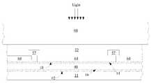
- FIG. 1is a cross-sectional view depicting a prior art photovoltaic cell.
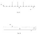
- FIG. 2is a graph of short-circuit current vs thickness of various silicon photovoltaic cells.
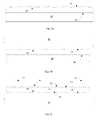
- FIGS. 3 a and 3 bare cross-sectional views showing stages in formation of a photovoltaic cell according to an embodiment of the present invention.
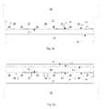
- FIGS. 4 a through 4 dare cross-sectional views showing stages in formation of a photovoltaic cell according to an embodiment of the present invention.
- FIGS. 5 a - 5 care cross-sectional views showing stages in formation of a photovoltaic cell according to an embodiment of the present invention.
- FIGS. 6 a and 6 bare cross-sectional views showing stages in formation of a photovoltaic cell according to another embodiment of the present invention.
- FIGS. 7 a - 7 care cross-sectional views showing stages in formation of a photovoltaic cell according to another embodiment of the present invention.
- FIGS. 8 a and 8 bare cross-sectional views showing stages in formation of a photovoltaic cell according to yet another embodiment of the present invention.
- FIGS. 9 a - 9 dare cross-sectional views showing stages in formation of a photovoltaic cell according to an embodiment of the present invention.
- FIGS. 10 a and 10 bare cross-sectional views showing stages in formation of a photovoltaic cell according to still another embodiment of the present invention.
- FIGS. 11 a and 11 bare cross-sectional views showing stages in formation of a photovoltaic cell according to still another embodiment of the present invention.
- FIGS. 12 and 13are cross-sectional views of alternative embodiments in which a lamina formed according to the present invention is a portion of a tandem or multijunction photovoltaic cell.
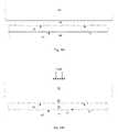
- FIG. 14is a plan view of a photovoltaic module comprising a plurality of thin photovoltaic cells according to an embodiment of the present invention.
- FIGS. 15 a - 15 care cross-sectional views showing stages in formation of an alternative embodiment of the present invention in which a lamina is transferred between a substrate and a superstrate.
- a typical silicon wafer used to make a photovoltaic cellis about 200 to 250 microns thick. It is known to slice silicon wafers as thin as about 180 microns, but such wafers are fragile and prone to breakage.
- a conventional prior art photovoltaic cellincludes a p-n diode; an example is shown in FIG. 1 .
- a depletion zoneforms at the p-n junction, creating an electric field.
- Incident photonswill knock electrons from the conduction band to the valence band, creating electron-hole pairs.
- electronstend to migrate toward the n region of the diode, while holes migrate toward the p region, resulting in current. This current can be called the photocurrent.
- the dopant concentration of one regionwill be higher than that of the other, so the junction is either a p ⁇ /n+ junction (as shown in FIG. 1 ) or a p+/n ⁇ junction.
- the more lightly doped regionis known as the base of the photovoltaic cell, while the more heavily doped region is known as the emitter. Most carriers are generated within the base, and it is typically the thickest portion of the cell. The base and emitter together form the active region of the cell.
- conversion efficiency of a photovoltaic cellvaries with its thickness.
- conversion efficiencyrefers to the fraction of incident photon current that is converted to usable electrical current.
- Light absorptioncan also be improved by increasing the distance light travels through the cell by bending it at an oblique angle or by internally reflecting it multiple times through the cell. Bending can be caused, for example, by texturing one or both surfaces of the cell, and reflection by coating one surface with a reflective material. These effects are known as light trapping.
- a surface that is textured such that the angles of transmitted and reflected light are fully randomizedis called a Lambertian surface. That is, for a Lambertian surface, the photon flux density per unit solid angle is independent of the direction of the incident light and position along the surface.
- FIG. 2is a graph showing theoretical short-circuit current density (J SC ) vs. thickness for various photovoltaic cells.
- J SCtheoretical short-circuit current density
- J SCis about 42 mA/cm 2 , while at 50 microns, J SC has dropped only slightly, to about 41 mA/cm 2 ; at 10 microns, J SC is still well above 35 mA/cm 2 .
- Substantially thinner photovoltaic cells, at 5, 2, 1, and even a fraction of a micron thick,can theoretically be made with commercially useful efficiencies, if they can be made at sufficiently low cost.
- a very thin semiconductor laminais cleaved from a semiconductor donor body, for example a monocrystalline or multicrystalline silicon wafer, by means other than conventional slicing, allowing the lamina to be much thinner.
- the laminacan be processed to form all or a portion of a photovoltaic cell.
- one or more species of gas ionsare implanted through a first surface 10 of a wafer 20 .
- the ionsare slowed by electronic interactions and by nuclear collisions with atoms in the lattice.
- the implanted ionsreach a distribution of depths, some deeper, some shallower. This distribution will have a maximum concentration at some depth below first surface 10 .
- the implant processresults in lattice damage, also at a distribution of depths.
- the damageconsists of vacant lattice sites created by displacement of the lattice atoms due to collisions with the incoming implanted atoms.
- This damagealso has a depth of maximum concentration, which is slightly shallower than the depth of the maximum concentration of implanted gas atoms.
- the implantdefines a cleave plane 30 along which a lamina can be cleaved from the wafer 20 .
- the depth of cleave plane 30can be between about 0.2 micron and about 100 microns.
- the implanted gas ionsmigrate to cleave plane 30 , forming bubbles or micro-cracks.
- the bubbles or micro-cracksexpand and merge, resulting in separation of lamina 40 from donor wafer 20 .
- first surface 10 of wafer 20is processed first, including, for example, doping with p-type and/or n-type dopants, texturing to increase light trapping, growth or deposition of films, etc.
- gas ionsare implanted through first surface 10 , defining subsurface cleave plane 30 .
- first surface 10is affixed or adhered to a planar surface 60 , which will be referred to as a receiver.
- a subsequent thermal annealcauses lamina 40 to exfoliate along previously defined cleave plane 30 ; this anneal may also serve to complete bonding of lamina 40 to receiver 60 .
- Cleavingcreates second surface 62 .
- Additional processingsuch as surface texturing, formation of an antireflective layer, doping, formation of wiring, etc., may be performed to second surface 62 .
- receiver 60can serve as either a substrate or a superstrate in the finished device, which may be a photovoltaic module.
- lamina 40may be temporarily transferred to receiver 60 , then transferred to some other substrate or superstrate.
- electrical contact to lamina 40is made only at first surface 10 or at second surface 62 , while in other embodiments, electrical contact is made at both first surface 10 and second surface 62 .
- Lamina 40having thickness between about 0.2 and about 100 microns, preferably between about 1 and about 10 microns; in some embodiments this thickness is between about 1 and about 5 microns.
- Lamina 40comprises or is a portion of a solar cell.
- Lamina 40has been processed on both sides and is affixed to a substrate or superstrate.
- a solar panel or photovoltaic modulecan be fabricated by affixing a plurality of laminae to the same substrate or superstrate. The plurality of laminae can be formed in the same steps, further reducing cost.
- a contiguous, monolithic semiconductor donor body having a first thicknessis provided.
- a different processis known in the art by which an epitaxially grown layer of crystalline silicon is first formed on, then separated from a porous silicon layer.
- a silicon wafermay be subjected to anodic etching, which forms a series of voids at or near the wafer surface.
- the voidstypically have dimensions of a micron or more.
- An anneal in hydrogenreconstructs a top surface of silicon having a separation layer of voids below it. Silicon is epitaxially grown on this reconstructed silicon layer by depositing silicon in a separate step on a single crystal substrate.
- the epitaxially grown layeris then separated from the original wafer at the separation layer.
- the material making up the separated layerwas grown, and is not a portion of the original wafer; thus the thickness of the wafer is not reduced by the thickness of the detached layer, only by the thickness of the separation layer consisting of voids formed by anodic etching.
- the semiconductor waferhas a layer on it which is epitaxially grown, and includes voids; it is not a contiguous, monolithic donor body.
- a contiguous, monolithic semiconductor donor bodyIn contrast, in the present invention, a contiguous, monolithic semiconductor donor body is provided.
- the donor bodyhas no voids.
- the cleaved laminais a portion of the contiguous, monolithic semiconductor donor body, not a separate layer which is epitaxially grown on the body by depositing silicon in a separate step on a single crystal substrate.
- cleaving the lamina from the donor bodyreduces the thickness of the original donor body by at least the thickness of the lamina.
- An effective way to cleave a thin lamina from a semiconductor donor bodyis by implanting gas ions into the semiconductor donor body to define a cleave plane, then to exfoliate the lamina along the cleave plane.
- a detailed examplewill be provided of how to perform implant and exfoliation. Note exfoliation is one form of cleaving. It will be understood that this example is provided for illustration only, and is not intended to be limiting. Many details of this example can be altered, omitted, or augmented while the result falls within the scope of the invention.
- one or more species of ionsis implanted (indicated by arrows) through first surface 10 of wafer 20 .
- gas ionsmay be used, including hydrogen (H+, H 2 +) and helium (He+, He++).
- hydrogen ions alone, or helium ions alone,may be implanted; in alternative embodiments, hydrogen ions or helium ions are implanted together.
- Each implanted ionwill travel some depth below first surface 10 . It will be slowed by electronic interactions and nuclear collisions with atoms as it travels through the lattice. The nuclear collisions may lead to displacement of the lattice atoms creating vacancies or vacant lattice sites, which are effectively damage to the lattice.
- the maximum concentration of damagewhich is slightly shallower than the maximum concentration of hydrogen ions, will generally be the cleave plane.
- the implantincludes helium, or some other gas ion, but does not include hydrogen, the maximum concentration of implanted ions will be the cleave plane. In either case, the ion implantation step defines the cleave plane, and implant energy defines the depth of the cleave plane.
- this cleave planecannot be a perfect plane, and will have some irregularities. If both hydrogen and helium ions are implanted, it is preferred for their maximum concentration to occur substantially at or near the same depth, though they may not be exactly the same. It is preferred, though not required, that the hydrogen implant is performed before the helium implant.
- gas ionsmay be implanted, including neon, crypton, argon, etc., either alone or in combination with helium, with hydrogen, or with hydrogen and helium; or indeed in any combination. These ions have larger mass, so higher implant energies are required to implant them to the same depth as a smaller mass ion.
- hydrogen atomspassivate dangling silicon bonds by forming Si-H bonds.
- Atomic hydrogenwill readily passivate the broken silicon bonds present at vacant lattice sites.
- multiple hydrogen atomswill bond to adjacent silicon atoms forming a platelet defect. Platelet defects are more fully described by Johnson et al., “Defects in single-crystal silicon induced by hydrogenation,” Phys. Rev. B 35, pp. 4166-4169 (1987), hereby incorporated by reference.
- Some hydrogen atomswill not bond with silicon, and will remain free in the lattice as either atomic or molecular hydrogen.
- Implanted helium atomsare inert and will not form bonds, and will thus remain free in the lattice.
- the ion implantation stepdefines cleave plane 30 for a subsequent cleaving step.
- the depth of cleave plane 30 from first surface 10in turn will determine the thickness of the lamina ultimately to be produced. As described earlier, this thickness affects the conversion efficiency of the completed cell.
- one or more thin filmsmay have been deposited or grown on first surface 10 before implantation.
- the depth of the implanted ionsis determined by the energy at which the gas ions are implanted. At higher implant energies, ions travel farther, increasing the depth of the maximum concentration of implanted ions, and the maximum concentration of damage, and thus the depth of the cleave plane. The depth of the cleave plane in turn determines the thickness of the lamina.
- Preferred thicknesses for the laminaare between about 0.2 and about 100 microns; thus preferred implant energies for H+ range from between about 20 keV and about 10 MeV. Preferred implant energies for He+ ions to achieve these depths also range between about 20 keV and about 10 MeV.
- collisionsmay occur between the ions being implanted and atoms in the ion implanter, At certain known energies, these collisions can cause nuclear reactions, creating gamma radiation, alpha particles, or x-rays. Depending on ion dose rate and shielding, it may be preferred to avoid the energies that will cause such reactions. The amount of radiation and its acceptability are however a function of ion dose rate and shielding. The topic is more fully discussed by Saadatmand et al., “Radiation Emission from Ion Implanters when Implanting Hydrogen and Deuterium,” Proceedings of the 1998 International Conference on Ion Implantation Technology, pp. 292-295, 1999.
- ionsare generated in the ion source by creating a plasma of some convenient source gas or solid. These ions are subsequently extracted from the source and mass analyzed to select only the desired ion species. There may be ions present in the plasma which are rejected by the mass analysis.
- implanterthere is no mass analysis and hence all of the ion species present in the source plasma are implanted into the wafer target. In the case of a hydrogen plasma, both H+ and H 2 + ions will likely be present. If the ions are not subject to mass analysis, both H+ and H 2 + will be implanted, creating two distribution peaks at different depths. This is less preferred, as it may render the subsequent exfoliation step more difficult to control. If hydrogen is implanted without mass analysis, it is advantageous to operate the source in a fashion that will produce a preponderance of either H+ ions or H 2 + ions.
- an implantleaves implanted ions at a variety of depths.
- a higher energy implantleaves more ions at depths shallower and deeper than the depth of the maximum concentration than does a lower energy implant, resulting in a broader distribution of implanted atoms.
- the cleaving processproceeds by diffusion of the gas atoms to the cleave plane; this broader distribution means that a higher implant dose is required for a higher energy implant.
- implant dose and energyshould be about 100 keV; for a lamina of about 2 microns, about 200 keV, for a lamina of about 5 microns, about 500 keV, and for a lamina of about 10 microns, about 1000 keV. If hydrogen alone is implanted, the dose for a lamina of about 1 or about 2 microns will range between about 0.4 ⁇ 10 17 and about 1.0 ⁇ 10 17 ions/cm 2 , while the dose for a lamina of about 5 or about 10 microns will range between about 0.4 ⁇ 10 17 and about 2.0 ⁇ 10 17 ions/cm 2 .
- hydrogen dose to form a lamina of about 1 or about 2 micronswill be between about 0.1 ⁇ 10 17 and about 0.3 ⁇ 10 17 ions/cm 2
- hydrogen dosemay be between about 0.1 ⁇ 10 17 and about 0.5 ⁇ 10 17 ions/cm 2 .
- implant energy for heliumshould be about 50 to about 200 keV; for a lamina of about 2 microns, about 100 to about 400 keV; for a lamina of about 5 microns, about 250 to about 1000 keV; and for a lamina of about 10 microns, about 500 keV to about 1000 keV.
- helium dose to form a lamina of about 1 or about 2 micronsmay be about 0.1 ⁇ 10 17 to about 0.3 ⁇ 10 17 ions/cm 2 , while to form a lamina of about 5 or about 10 microns, helium dose may be between about 0.1 ⁇ 10 17 and about 0.5 ⁇ 10 17 ions/cm 2 .
- energies and dosesmay vary, and intermediate energies may be selected to form laminae of intermediate, lesser, or greater thicknesses.
- wafer 20can be affixed to receiver 60 .
- exfoliation of a lamina 40is most readily effected by increasing temperature.
- the earlier implant stepleft a distribution of gas ions, and a distribution of lattice damage in the donor silicon wafer, where the implant defined cleave plane 30 .
- hydrogenwas implanted, many hydrogen ions broke silicon bonds during collisions with silicon atoms and passivated those bonds, in some cases forming platelet defects, as described earlier.
- platelet defectsare on the order of 30 to 100 angstroms wide, less than 200 angstroms wide, at room temperature.
- the waferis a contiguous, monolithic semiconductor donor body having no voids larger than the platelet defects.
- Receiver 60 with affixed wafer 20is subjected to elevated temperature, for example between about 200 and about 800 degrees C. Exfoliation proceeds more quickly at higher temperature.
- the temperature step to induce exfoliationis performed at between about 200 and about 500 degrees C., with anneal time on the order of hours at 200 degrees C., and on the order of seconds at 500 degrees C.
- the platelet defectsbegin to expand as more and more of the unbonded gas atoms diffuse in all directions, some collecting in the platelet defects, and forming micro-cracks.
- the micro-cracksmerge and the pressure exerted by the expanding gas causes lamina 40 to separate entirely from the donor silicon wafer 20 along cleave plane 30 .
- receiver 60forces the micro-cracks to expand sideways, forming a continuous split along cleave plane 30 , rather than expanding perpendicularly to cleave plane 30 prematurely, which would lead to blistering and faking at first surface 10 .
- platelet defectswill only form when hydrogen is implanted. If helium or other gas ions are implanted without hydrogen, the implanted atoms will form micro-cracks or bubbles that fill up with gas, then cleave along cleave plane 30 .
- wafer 20is p-doped with boron, a common p-type dopant, exfoliation may be achieved at a slightly lower temperature than if it is intrinsic or lightly n-doped.
- FIG. 4 dshows the structure inverted, with receiver 60 on the bottom. It will be seen that lamina 40 is created by the cleaving step, and that lamina 40 comprises first surface 10 , and has a second surface 62 substantially parallel to first surface 10 . As will be described, lamina 40 comprises or is, or will be, a portion of a photovoltaic cell. First surface 10 remains affixed to receiver 60 . In some embodiments the elevated temperature used to perform the exfoliation will also serve to simultaneously complete the bonding process between first surface 10 and receiver 60 .
- silicon-on-insulator filmsfor use in the semiconductor industry by implanting gas ions into a silicon wafer, bonding the silicon wafer to an oxide wafer, and exfoliating a thin skin of silicon onto the oxide wafer. Semiconductor devices, such as transistors are then fabricated in the exfoliated silicon skin.
- Ion implantationis widely used in fabrication of semiconductor devices, but has been considered impractical for widespread use in the solar industry, as keeping processing cost low is generally paramount for solar manufacturers.
- Typical high-dose implants used in the semiconductor industryare in the range of 1 ⁇ 10 14 to 3 ⁇ 10 15 ions/cm 2 at energies up to about 80 keV. Exfoliating a lamina having a thickness of 1-10 microns, for example, requires implant energy of hundreds of keV, and at relatively high doses, for example 4 ⁇ 10 16 to 2 ⁇ 10 17 ions/cm 2 . Higher implant dose at higher energy increase the cost of the implant.
- the inventors of the present inventionhave recognized that a lamina of 100 microns or less, for example 10 microns or less, can be used to form a photovoltaic cell with acceptable conversion efficiency, even where the lamina comprises all or portions of the base and/or emitter, the active regions of the cell.
- the implantation of gas ions in the embodiments described hereincan be performed today on existing implanters. The inventors believe that use of a specialized, high-throughput implanter would substantially reduce the cost of this implant.
- a lamina having thickness between 0.2 and 100 micronswhere the lamina comprises, or is a portion of, a photovoltaic cell according to embodiments of the present invention.
- many materials, conditions, and stepswill be described. It will be understood, however, that many of these details can be modified, augmented, or omitted while the results fall within the scope of the invention.
- Other methods of cleaving a lamina from a semiconductor wafercould also be employed in these embodiments.
- An appropriate donor body 20 of an appropriate semiconductor materialmay be a monocrystalline silicon wafer of any practical thickness, for example from about 300 to about 1000 microns thick. In alternative embodiments, the wafer may be thicker; maximum thickness is limited only by practicalities of wafer handling.
- polycrystalline or multicrystalline siliconmay be used, as may microcrystalline silicon, or wafers or ingots of other semiconductors materials, including germanium, silicon germanium, or III-V or II-VI semiconductor compounds such as GaAs, InP, etc.
- multicrystallinetypically refers to semiconductor material having crystals that are on the order of a millimeter in size, while polycrystalline semiconductor material has smaller grains, on the order of a thousand angstroms.
- microcrystalline semiconductor materialare very small, for example 100 angstroms or so.
- Microcrystalline siliconfor example, may be fully crystalline or may include these microcrystals in an amorphous matrix.
- Multicrystalline or polycrystalline semiconductorsare understood to be completely or substantially crystalline.
- the process of forming monocrystalline silicongenerally results in circular wafers, but the donor body can have other shapes as well.
- Cylindrical monocrystalline ingotsare often machined to an octagonal cross section prior to cutting wafers.
- Multicrystalline wafersare often square. Square wafers have the advantage that, unlike circular or hexagonal wafers, they can be aligned edge-to-edge on a photovoltaic module with no unused gaps between them.
- the diameter or width of the wafermay be any standard or custom size. For simplicity this discussion will describe the use of a monocrystalline silicon wafer as the semiconductor donor body, but it will be understood that donor bodies of other types and materials can be used.
- wafer 20is formed of monocrystalline silicon which is preferably lightly doped to a first conductivity type.
- the present examplewill describe a relatively lightly p-doped wafer 20 but it will be understood that in this and other embodiments the dopant types can be reversed.
- Dopant concentrationmay be between about 1 ⁇ 10 14 and 1 ⁇ 10 18 atoms/cm 3 ; for example between about 3 ⁇ 10 14 and 1 ⁇ 10 15 atoms/cm 3 ; for example about 5 ⁇ 10 14 atoms/cm 3 .
- Desirable resistivity for p-type siliconmay be, for example, between about 133 and about 0.04 ohm-cm, preferably about 44 to about 13.5 ohm-cm, for example about 27 ohm-cm.
- desirable resistivitymay be between about 44 and about 0.02 ohm-cm, preferably between about 15 and about 4.6 ohm-cm, for example about 9 ohm-cm.
- First surface 10is optionally treated to produce surface roughness, for example, to produce a Lambertian surface.
- the ultimate thickness of the laminalimits the achievable roughness. In conventional silicon wafers for photovoltaic cells, surface roughness, measured peak-to-valley, is on the order of a micron.
- the thickness of the laminamay be between about 0.2 and about 100 microns. Preferred thicknesses include between about 1 and about 80 microns; for example, between about 1 and about 20 microns or between about 2 and about 20 microns. Practically, any thickness in the range between about 0.2 and about 100 microns is achievable; advantageous thicknesses may be between about 1 and about 1.5, 2, 3, 5, 8, 10, 20, or 50 microns.
- a lower limit of surface roughnesswould be about 500 angstroms.
- An upper limitwould be about a quarter of the film thickness.
- surface roughnessmay be between about 600 angstroms and about 2500 angstroms.
- surface roughnesswill be less than about 25000 angstroms, for example between about 600 angstroms and 25000 angstroms.
- surface roughnessmay be between about 600 angstroms and 50000 angstroms.
- This surface roughnesscan be produced in a variety of ways which are well-known in the art. For example, a wet etch such as a KOH etch selectively attacks certain planes of the silicon crystal faster than others, producing a series of pyramids on a ( 100 ) oriented wafer, where the ( 111 ) planes are preferentially etched faster. A non-isotropic dry etch may be used to produce texture as well. Any other known methods may be used. The resulting texture is depicted in FIG. 5 a .
- Surface roughnessmay be random or may be periodic, as described in “Niggeman et al., “Trapping Light in Organic Plastic Solar Cells with Integrated Diffraction Gratings,” Proceedings of the 17 th European Photovoltaic Solar Energy Conference, Kunststoff, Germany, 2001.
- diffusion dopingmay be performed at first surface 10 .
- First surface 10will be more heavily doped in the same conductivity type as original wafer 20 , in this instance p-doped.
- Dopingmay be performed with any conventional p-type donor gas, for example B 2 H 6 or BCl 3 . In other embodiments, this diffusion doping step can be omitted.
- Next ionspreferably hydrogen or a combination of hydrogen and helium, are implanted to define a cleave plane 30 , as described earlier.
- a thin oxide layer 19which may be about 100 angstroms or less on first surface 10 .
- Oxide layer 19may serve to reduce surface damage during the implant.
- This oxidegenerally silicon dioxide, can be formed by any conventional method. If diffusion doping is performed before the implant, providing some oxygen during diffusion doping will cause silicon dioxide layer 19 to grow.
- first surface 10is cleaned.
- exfoliationwill occur once certain conditions, for example elevated temperature, are encountered. It is necessary, then, to keep processing temperature and duration below those which will initiate exfoliation until exfoliation is intended to take place.
- this receiveris in fact a superstrate or substrate which will be part of the photovoltaic module after fabrication is complete.
- This receivermay be any appropriate material, such as semiconductor, glass, metal, or polymer.
- the receiver to which first surface 10 is affixedis a substrate 60 .
- substrate 60may be borosilicate glass or some other material that can tolerate relatively high temperature.
- a reflective metallic materialfor example titanium or aluminum
- Other alternatives for such a layerinclude chromium, molybdenum, tantalum, zirconium, vanadium, or tungsten.
- aluminumcan be sputter deposited onto first surface 10 .
- the surface of substrate 60may be coated with aluminum or some other reflective metallic material. Subsequent thermal steps will soften the aluminum, causing it to flow and make good contact with first surface 10 .
- an aluminum layercan be formed on both first surface 10 and on substrate 60 .
- lamina 40can now be cleaved from donor wafer 20 at cleave plane 30 as described earlier.
- Second surface 62has been created by exfoliation.
- the structureis shown inverted, with substrate 60 on the bottom.
- some surface roughnessis desirable to increase light trapping within lamina 40 and improve conversion efficiency of the photovoltaic cell.
- the exfoliation processitself creates some surface roughness at second surface 62 . In some embodiments, this roughness may alone be sufficient. In other embodiments, surface roughness of second surface 62 may be modified or increased by some other known process, such as a wet or dry etch, as may have been used to roughen first surface 10 .
- metal 12is a p-type acceptor such as aluminum, annealing at this point or later may serve to form or additionally dope p-doped region 16 by causing metal atoms from metal layer 12 to diffuse into region 16 .
- a region 14 at the top of lamina 40is doped through second surface 62 to a conductivity type opposite the conductivity type of the original wafer 20 .
- original wafer 20was lightly p-doped, so doped region 14 will be n-type.
- This dopingmay be performed by any conventional means. In preferred embodiments this doping step is performed by diffusion doping using any appropriate donor gas that will provide an n-type dopant, for example POCl 3 .
- Diffusion dopingis typically performed at relatively high temperature, for example between about 700 and about 900 degrees C., although lower temperature methods, such as plasma enhanced diffusion doping, can be performed instead.
- This elevated temperaturewill cause some aluminum from aluminum layer 12 to diffuse in at first surface 10 .
- This elevated temperaturecan serve as the anneal mentioned earlier to form a more heavily doped p-type region 16 which will serve to form a good electrical contact to aluminum layer 12 .
- doping of p-region 16 from aluminum layer 12is sufficient, the earlier diffusion doping step performed at first surface 10 to form this region can be omitted.
- a thin layer of silicon dioxide(not shown) will form at second surface 62 .
- Antireflective layer 64is preferably formed, for example by deposition or growth, on second surface 62 . Incident light enters lamina 40 through second surface 62 ; thus this layer should be transparent.
- antireflective layer 64is silicon nitride, which has a refractive index of about 1.5 to 3.0; its thickness would be, for example, between about 500 and 2000 angstroms, for example about 650 angstroms.
- Next wiring 57is formed on layer 64 .
- this wiringis formed by screen printing conductive paste in the pattern of wiring, which is then fired at high temperature, for example between about 700 and about 900 degrees C.
- layer 64is silicon nitride
- FIG. 5 cshows a completed photovoltaic cell according to one embodiment of the present invention.
- Lamina 40is bonded to substrate 60 at first surface 10 .
- Incident lightenters lamina 40 at second surface 62 .
- the lightly p-doped body of lamina 40is the base of this cell, while heavily doped n-region 14 is the emitter; thus lamina 40 comprises a photovoltaic cell.
- Currentis generated within lamina 40 when it is exposed to light. Electrical contact is made to both first surface 10 and second surface 62 of this cell. Wiring 57 is in electrical contact with second surface 62 .
- wiring 57may be preferred to form wiring 57 by other methods.
- fabrication of this embodimentis the same as for the prior embodiment up to the point at which silicon nitride layer 64 has been formed on second surface 62 .
- a series of parallel trenches 68are formed in silicon nitride layer 64 , exposing the silicon of second surface 62 in each trench 68 .
- Trenches 68can be formed by any appropriate method, for example by photolithographic masking and etching.
- a second diffusion doping step with an n-type dopantcan be performed at this point, more heavily doping silicon exposed in trenches 68 .
- FIG. 6 bshows wiring 57 , which is formed contacting n-doped region 14 exposed in trenches 57 .
- Wiring 57can be formed by any convention means. It may be preferred to form a metal layer on silicon nitride layer 64 , then form wiring 57 by photolithographic masking and etching. In an alternate embodiment, wiring 57 is formed by screen printing, for example to form aluminum wiring.
- electrical contact at the back surface of the cellis made locally.
- this embodimentbegins with lightly p-doped wafer 20 , which is optionally roughened at first surface 10 as in earlier embodiments.
- Dielectric layer 55which will act as a diffusion barrier, is deposited on first surface 10 .
- dielectric layer 55is silicon nitride or SiO 2 , and may be between about 1000 and about 1200 angstroms.
- Vias 68are formed in silicon nitride layer 55 , exposing first surface 10 in each via 68 . Note that in preferred embodiments, vias 68 are vias, not trenches.
- a diffusion doping stepis performed, doping exposed areas of first surface 10 with a p-type dopant and forming heavily doped p-type regions 16 . In some embodiments this diffusion doping step may be omitted. Next gas ions are implanted as before, defining cleave plane 30 .
- aluminum layer 11is formed on silicon nitride layer 55 , filling the vias and contacting heavily doped p-type regions 16 .
- aluminum layer 11may be about 1 micron thick.
- Next wafer 20is affixed to substrate 60 at first surface 10 .
- FIG. 7 cwhich shows the structure inverted with substrate 60 at the bottom, fabrication continues as in previous embodiments.
- Lamina 40is formed by exfoliation from wafer 20 , creating second surface 62 .
- Second surface 62may be roughened, as in prior embodiments.
- An n-doped region 14is formed by diffusion doping at second surface 62 . Elevated temperature during this diffusion doping step causes some aluminum from aluminum layer 11 to diffuse into lamina 40 where it contacts silicon at first surface 11 , further doping p-doped regions 16 .
- Antireflective layer 64is formed on second surface 62 .
- a thin oxide layer(not shown) may have grown on second surface 62 during the diffusion doping step to form n-doped layer 14 .
- Wiring 57is formed, by screen printing, photolithography, or by some other method, completing the cell.
- the heavily doped regions of the cellare formed in amorphous semiconductor layers.
- original wafer 20is lightly n-doped (as always, in alternate embodiments, conductivity types can be reversed.)
- First surface 10 of wafer 20is optionally roughened as in prior embodiments. After cleaning first surface 10 , a layer 72 of intrinsic (undoped) amorphous silicon is deposited on first surface 10 , followed by a layer 74 of n-doped amorphous silicon by any suitable method, for example by plasma enhanced chemical vapor deposition (PECVD).
- PECVDplasma enhanced chemical vapor deposition
- the combined thickness of amorphous layers 72 and 74may be between about 1000 and about 5000 angstroms, for example about 3000 angstroms.
- intrinsic layer 72is about 1000 angstroms thick
- n-type amorphous layer 74is about 2000 angstroms thick.
- Gas ionsare implanted through layers 74 , 72 and into first surface 10 to form cleave plane 30 as in prior embodiments. It will be understood that the implant energy must be adjusted to compensate for the added thickness of amorphous layers 74 and 72 .
- a reflective, conductive metal 11is formed on n-doped layer 74 , on substrate 60 , or both, as in prior embodiments, and wafer 20 is affixed to substrate 60 at first surface 10 , with intrinsic layer 72 , n-doped layer 74 , and metal layer 11 intervening between them.
- Metal layer 11can be aluminum, titanium, or any other suitable material.
- metal layer 11may have been deposited in a pattern, such that the areas to which individual wafers are to be affixed are isolated from each other. These areas of metal 11 may extend for a short distance outside of the wafer area, so that electrical contact can be made to them. This patterning can be done, for example, by depositing through a shadow mask; or by etching metal 11 after it is deposited, for example, through a physical mask placed on substrate 60 .
- FIG. 8 bshows the structure inverted, with substrate 60 at the bottom.
- Lamina 40is exfoliated from wafer 20 along cleave plane 30 , creating second surface 62 .
- Second surface 62is optionally roughened, and is cleaned.
- Intrinsic amorphous silicon layer 76is deposited on second surface 62 , followed by p-doped amorphous silicon layer 78 .
- the thicknesses of intrinsic amorphous layer 76 and p-doped amorphous layer 78may be about the same as intrinsic amorphous layer 72 and n-doped amorphous layer 74 , respectively, or may be different.
- antireflective layer 64which may be, for example, silicon nitride, is formed on p-type amorphous layer 78 by any suitable method.
- antireflective layer 64may be a transparent conductive oxide (TCO). If this layer is a TCO, it may be, for example, of indium tin oxide, tin oxide, titanium oxide, zinc oxide, etc.
- TCOwill serve as both a top electrode and an antireflective layer and may be between about 500 and 1500 angstroms thick, for example, about 900 angstroms thick.
- wiring 57is formed on antireflective layer 64 .
- Wiring 57can be formed by any appropriate method. In a preferred embodiment, wiring 57 is formed by screen printing.
- lamina 40is the base, or a portion of the base, of a photovoltaic cell.
- Heavily doped p-type amorphous layer 78is the emitter, or a portion of the emitter.
- Amorphous layer 76is intrinsic, but in practice, amorphous silicon will include defects that cause it to behave as if slightly n-type or slightly p-type. If it behaves as if slightly p-type, then, amorphous layer 76 will function as part of the emitter, while if it behaves as if slightly n-type, it will function as part of the base.
- a plurality of these cellsis formed at one time onto a single substrate 60 .
- Deposition of p-type amorphous layer 78 and, if it was a TCO, of antireflective layer 64 onto multiple laminae affixed to the same substrate 60 in the same deposition stepleaves adjacent laminae electrically connected through these layers.
- These layersmust be electrically separated before formation of wiring 57 , for example by etching these layers through a physical mask that is placed on the substrate/lamina assembly, or by ablating the layers away with a laser.
- the individual cellsshould be wired together, typically in a series configuration, in which the N+ electrode of one cell is connected to the P+ electrode of the adjacent cell.
- Thiscan be done by patterning wiring 57 during its formation so as to make contact to metal surfaces already patterned on substrate 60 , if any.
- wiring 57can be connected to metal patterns in substrate 60 by individual soldering. If there is no metal patterning in substrate 60 , a laser can be used to ablate the entire lamina 40 from a small area, for example about a square cm, of each lamina 40 , exposing the metal underneath. This exposed metal can be connected to wiring 57 of the neighboring lamina by soldering, for example.
- lightly doped wafer 20 of either typethis example will describe initial wafer 20 as lightly p-doped, but it will be understood that either conductivity type can be used.
- First surface 10is optionally roughened, and doped with a first conductivity type dopant, for example p-type, forming p-doped region 16 . Doping may be performed by diffusion doping.
- a diffusion barrier 32is deposited on first surface 10 ; diffusion barrier 32 may be Silicon nitride.
- FIG. 9 bareas of silicon nitride layer 32 are removed, exposing portions of first surface 10 .
- a second doping stepis performed, counterdoping the exposed areas of first surface 10 to a second conductivity type opposite the first, for example n-type, forming n-doped regions 14 , which are depicted in cross-hatching.
- n-doped regions 14 and p-doped regions 16are doped to a concentration of at least 10 18 atoms/cm 3 .
- next silicon nitride layer 32is removed, and ions are implanted to define a cleave plane 30 .
- a dielectric layer 18for example silicon dioxide, is deposited or grown on first surface 10 . Vias are etched in dielectric layer 18 , and wiring is formed on dielectric layer 18 . Wiring is formed in two electrically isolated sets; one wiring set 57 contacts n-doped regions 14 , while another wiring set 58 contacts p-doped regions 16 . Wiring sets 57 and 58 may be formed by depositing a metal and patterning it photolithographically.
- a dielectric 22such as spin-on glass fills gaps between wiring sets 57 and 58 and makes a relatively planar surface. This surface is affixed to substrate 60 . Exfoliation is cleaner and more controllable when the surface is planar and uniformly affixed to the receiver, in this case substrate 60 .
- FIG. 9 dshows the structure inverted with substrate 60 on the bottom.
- Lamina 40is cleaved from wafer 20 along cleave plane 30 , forming second surface 62 .
- Second surface 62is preferably roughened by any known method.
- second surface 62is doped to the same conductivity type as that of initial wafer 20 .
- initial wafer 20was n-type; thus this surface may be doped with an n-type dopant by diffusion doping to form n-doped region 17 . It may be preferred to flow some oxygen during this diffusion doping step, which will cause a thin silicon dioxide layer (not shown) to form; this thin silicon dioxide layer will help passivate dangling bonds at second surface 62 , reducing recombination.
- antireflective layer 64may be silicon nitride. Silicon nitride deposited by PECVD will include some hydrogen, and this hydrogen will tend to passivate these dangling bonds at second surface 62 , decreasing recombination. Deposition conditions may be chosen to increase the hydrogen content of silicon nitride layer 64 to increase the amount of hydrogen for this purpose.
- electrical contact in the form of wiring sets 57 and 58is made only to first surface 10 .
- the p-n diode junctionis formed between heavily doped p-regions 16 and the lightly n-doped body of lamina 40 .
- Photocurrentflows between n-doped regions 14 and p-doped regions 16 .
- the base of the photovoltaic cellis the lightly n-doped body of lamina 40
- the emitteris the combined heavily doped p-type regions 16 ; thus lamina 40 comprises both the base and emitter of a photovoltaic cell.
- currentis generated within lamina 40 when it is exposed to light.
- the laminais exfoliated to a substrate, where the first surface, the original surface of the donor body, is the back surface of the finished cell, and the second surface created by exfoliation is the surface where light enters the cell.
- the laminamay instead be exfoliated to a superstrate, where the original surface of the donor body is the surface where light enters the cell, while the second surface, created by exfoliation, is the back surface of the finished cell.
- semiconductor donor body 20is a lightly p-doped silicon wafer.
- First surface 10 of wafer 20is optionally textured as in prior embodiments.
- a doping stepfor example by diffusion doping, forms n-doped region 14 . If oxygen is present during this doping step, a thin oxide (not shown) will grow at first surface 10 . It will be understood that, as in all embodiments, conductivity types can be reversed. Gas ions are implanted through first surface 10 to define cleave plane 30 .
- First surface 10is cleaned, removing any oxide formed during diffusion doping.
- TCO 80will intervene between first surface 10 and superstrate 60 .
- This TCO 80is indium tin oxide, titanium oxide, zinc oxide, or any other appropriate material, and can be deposited on first surface 10 , on superstrate 60 , or both.
- Wafer 20is affixed to superstrate 60 at first surface 10 .
- superstrate 60is a transparent material such as glass.
- lamina 40is exfoliated from wafer 20 at cleave plane 30 , creating second surface 62 .
- Second surface 62is optionally textured.
- Conductive layer 11is deposited on second surface 62 .
- Conductive layer 11is preferably a metal, for example aluminum. If conductive layer 11 is aluminum, an anneal forms p-doped layer 16 . If some other material is used for conductive layer 11 , p-doped layer 16 must be formed by a diffusion doping step before conductive layer 11 is formed.
- Aluminum layer 11can be formed by many methods, for example by sputtering with a shadow mask. If the method of formation of aluminum layer 11 leaves adjacent cells electrically connected, intervening aluminum must be removed to electrically isolate them.
- FIG. 10 bshows the completed cell with superstrate 60 at the top, as during operation. Incident light falls on superstrate 60 and enters the cell at first surface 62 .
- lightly p-doped wafer 20is optionally textured at first surface 10 , then doped to form n-type region 14 .
- Implantation of gas ions at first surface 10forms cleave plane 30 .
- antireflective layer 64for example silicon nitride
- first surface 10for example by PECVD.
- Trenchesare formed in silicon nitride layer 64 , for example by photolithography or by laser scribing, to expose first surface 10 .
- Wiring 57is formed contacting n-doped region 14 .
- Wiringcan be formed of any appropriate conductive material, for example aluminum, by any appropriate method, for example photolithographic masking and etching.
- Next dielectric 22such as spin-on glass fills gaps between wiring 57 and makes a relatively planar surface. This surface is affixed to superstrate 60 .
- Superstrate 60is transparent.
- lamina 40is exfoliated from wafer 20 at cleave plane 30 , creating second surface 62 .
- Second surface 62is optionally textured.
- a diffusion doping stepis performed, forming p-doped region 16 , while in other embodiments this step can be omitted.
- Conductive layer 11preferably aluminum, is formed on second surface 62 and an anneal will form p-doped region 16 .
- FIG. 11 bshows the completed cell with superstrate 60 at the top, as it will be during cell operation.
- a lamina formed according to the present inventionmay serve as a portion of a tandem or multijunction cell.
- the substrate 60 to which lamina 40 is affixedmay already include a photovoltaic cell or portion of a cell 90 ; incident light will fall first on lamina 40 , then pass through it to cell 90 .
- another cell or portion of a cell 92may be formed above lamina 40 , such that incident light travels first through cell 92 , then through lamina 40 .
- the other cellscan be formed of the same semiconductor material as lamina 40 or of a different semiconductor material; examples include germanium, silicon germanium, GaAs, CdTe, InN, etc.
- Lamina 40can include at least a portion of the base, or of the emitter, of a photovoltaic cell, or both.
- Lamina 40 and additional cells or semiconductor layers in a tandem or multijunction cellmay be the same semiconductor material, but may have a different degree or grade of crystallinity.
- lamina 40may be monocrystal line silicon while an additional cell or semiconductor layer is polycrystalline, multicrystalline, microcrystalline, or amorphous silicon, or vice versa.
- the additional cells forming the tandem or multifunction cellcan be formed in a variety of ways, for example by deposition, by evaporation, by epitaxial growth, by cleaving additional laminae according to the present invention, or by any other suitable methods.
- the semiconductor donor bodymay be subjected a second time to the implant and exfoliation processes just described to form a second lamina.
- This second laminamay similarly be affixed to a receiver and comprise, or be a portion of, a photovoltaic cell, or may be used for a different purpose.
- many laminaemay be formed, until the donor body is too thin to handle safely. It may be preferred to form one or more laminae, then resell the donor body for another purpose.
- laminaemay be formed by the methods described until the thickness of the donor wafer has been reduced to, for example, about 350 microns.
- the wafermay be resold with little or no loss of commercial value.
- the donor waferis preferably at least 180 microns thick. A wafer at least 180 microns thick can still be used for other commercial purposes.
- one or more laminaecan be formed from a wafer without substantially decreasing the value of the donor wafer, the material cost is dramatically reduced.
- materials that have previously been considered impractical for use in a photovoltaic cellnow become economically viable.
- Float-zone silicon wafersfor example, are very high-quality wafers which have been heat-treated to remove impurities.
- float-zone siliconis too expensive for economical use in silicon photovoltaic cells.
- laminae of float-zone siliconcan be cheaply produced, improving the efficiency of the resulting photovoltaic cell.
- the waferAfter cleaving one or more laminae from the float-zone silicon wafer, the wafer can be resold and used for another purpose.
- Other higher-cost source materialssuch as wafers of semiconductor materials besides silicon, for example monocrystalline GaAs or mono- or multicrystalline germanium wafers, may also be advantageous.
- a photovoltaic module including multiple laminae formed by methods according to the present inventionmay be fabricated.
- a plurality of donor bodiessuch as silicon wafers can be processed as described, implanted with gas ions, bonded or otherwise affixed to a single receiver 88 which is a substrate or a superstrate, and a lamina 40 cleaved from each donor wafer in a single cleaving step.
- the modulecomprises the receiver 88 and the laminae 40 .
- Such a modulemay include a plurality of laminae 40 , for example two, twelve, or more, for example between 36 and 72, or more, or any other suitable number.
- Each lamina 40comprises or is a portion of a photovoltaic cell, for example at least a portion of its base or emitter.
- the photovoltaic cells on the moduleare electrically connected; they may be connected in series, as is well known in the art.
- wafer 20could be affixed at its first surface 10 to a temporary, high-temperature-tolerant receiver 61 .
- the second surface 62could be exposed to high temperature processes, for example diffusion doping, without damaging the temporary receiver 61 .
- lamina 40when processing is complete, lamina 40 could be removed from temporary receiver 61 and transferred to a final receiver 60 . It is anticipated that multiple transfers would add cost and reduce yield, however, so these embodiments, while within the scope of the invention, are generally less preferred.
- the laminacomprises or is a portion of a photovoltaic cell.
- the laminamay or may not be formed of a semiconductor material, and may be used for different purposes.
- the methods of the present inventionmay be useful in any circumstance in which a thin lamina of material is to be affixed to a receiver; the receiver may be semiconductor, metal, polymer, or some non-insulating material.
- a semiconductor lamina of one conductivity type or dopant concentrationmay be affixed to a semiconductor receiver, or a receiver having a semiconductor layer, doped to a different conductivity type or a different dopant concentration.
Landscapes
- Photovoltaic Devices (AREA)
Abstract
Description
- The invention relates to a method to form a thin semiconductor lamina for use in a photovoltaic cell.
- Conventional photovoltaic cells are most commonly formed from silicon wafers. Typically such wafers are sliced from an ingot of silicon. Current technology does not allow wafers of less than about 170 microns thick to be fabricated into cells economically, and at this thickness a substantial amount of silicon is wasted in cutting loss, or kerf. Silicon solar cells need not be this thick to be effective or commercially useful. A large portion of the cost of conventional solar cells is the cost of silicon feedstock.
- There is a need, therefore, for a method to form a thinner crystalline semiconductor photovoltaic cell cheaply and reliably.
- The present invention is defined by the following claims, and nothing in this section should be taken as a limitation on those claims. In general, the invention is directed to a thin semiconductor lamina for use in a photovoltaic cell and methods for making such a cell.
- A first aspect of the invention provides for a method for forming a photovoltaic cell, the method comprising: providing a contiguous, monolithic semiconductor donor body having a first donor thickness; and cleaving a portion of the contiguous, monolithic semiconductor donor body to form a first lamina of semiconductor material, wherein the first lamina of semiconductor material has a first lamina thickness, the first lamina thickness between about 0.2 micron and about 100 microns thick; and fabricating the photovoltaic cell, wherein the first lamina of semiconductor material comprises at least a portion of the base or of the emitter, or both, of the photovoltaic cell.
- Another aspect of the invention provides for a method for fabricating a photovoltaic cell, the method comprising: implanting hydrogen ions into a semiconductor donor body through a first surface of the semiconductor donor body, wherein ion implantation defines a cleave plane at a depth below the first surface of between about 0.2 micron and about 100 microns; cleaving a lamina of semiconductor material from the donor body along the cleave plane; and fabricating the photovoltaic cell, wherein the lamina comprises at least a portion of the base or of the emitter, or both, of the photovoltaic cell.
- Still another aspect of the invention provides for a method for fabricating a photovoltaic cell, the method comprising: affixing a first surface of a first contiguous, monolithic semiconductor donor body to a receiver; after the affixing step, cleaving a first lamina of semiconductor material from the first donor body, wherein the first lamina of semiconductor material includes the first surface and remains affixed to the receiver, and fabricating the photovoltaic cell, wherein the first lamina of semiconductor material comprises at least a portion of the base or of the emitter, or both, of the photovoltaic cell.
- An embodiment of the invention provides for a method for fabricating a photovoltaic cell, the method comprising: doping at least portions of a first surface of a semiconductor wafer; implanting hydrogen ions through the first surface; affixing the first surface to a receiver; and after the affixing step, cleaving a first semiconductor lamina from the semiconductor wafer, wherein the first lamina comprises the first surface, wherein the first surface is bonded to the receiver, wherein current is generated within the first lamina when it is exposed to light.
- Another embodiment of the invention provides for a method for making a photovoltaic module, the method comprising: affixing a plurality of semiconductor wafers to a receiver; and after the affixing step, cleaving a semiconductor lamina from each of the semiconductor wafers, wherein each lamina is bonded to the receiver, wherein the photovoltaic module comprises the receiver and the laminae.
- Still another aspect of the invention provides for a semiconductor lamina comprising a photovoltaic cell, the semiconductor lamina having substantially parallel first and second surfaces, wherein a thickness between the first and second surfaces is between about 0.2 and about 100 microns, wherein wiring contacts the first surface but no wiring contacts the second surface, and wherein incident light enters the photovoltaic cell through the second surface.
- Another embodiment of the invention provides for a semiconductor lamina comprising a photovoltaic cell, the semiconductor lamina having substantially parallel first and second surfaces, wherein a thickness between the first and second surfaces is between about 0.2 and about 100 microns, wherein wiring contacts the first surface but no wiring contacts the second surface, and wherein incident light enters the photovoltaic cell through the second surface.
- Still another embodiment of the invention provides for a lamina of semiconductor material, the lamina of semiconductor material having substantially parallel first and second surfaces, wherein the distance between the first and second surfaces is between about 1 micron and about 100 microns, wherein peak-to-valley surface roughness of the first surface or the second surface is greater than about 600 angstroms, and wherein the lamina comprises a photovoltaic cell or a portion of a photovoltaic cell.
- An embodiment of the invention provides for a photovoltaic module comprising: a receiver; and a plurality of semiconductor laminae bonded to the receiver, wherein each semiconductor lamina is between about 1 and about 100 microns thick, wherein each semiconductor lamina comprises at least a portion of a base, or of an emitter, of a photovoltaic cell. A related embodiment provides for a photovoltaic module comprising: a plurality of laminae, each lamina having a thickness between about 0.2 and about 100 microns, each lamina comprising at least a portion of a base or of an emitter of a photovoltaic cell; and a substrate, wherein each lamina is bonded to the substrate. Still another related embodiment provides for a photovoltaic module comprising: a plurality of laminae, each lamina having a thickness between about 0.2 and about 100 microns, each lamina comprising at least a portion of a base or of an emitter of a photovoltaic cell; and a superstrate, wherein each lamina is bonded to the superstrate.
- Another aspect of the invention provides for a method for forming a device, the method comprising: adhering a first surface of a semiconductor body to a receiver, wherein the receiver is metal or polymer; and cleaving a lamina from the semiconductor body, wherein the lamina comprises the first surface, the first surface remains adhered to the receiver, and the lamina is between 1 and 80 microns thick.
- Another aspect of the invention provides for a method for forming multiple laminae, the method comprising: cleaving a first lamina from a semiconductor wafer, wherein the semiconductor wafer has a first thickness less than about 1000 microns and the first lamina has a thickness of about 1 micron or more; and after cleaving the first lamina, cleaving a second lamina from the semiconductor wafer, wherein the second lamina has a thickness of about one micron or more, wherein, after cleaving the second lamina, the semiconductor wafer has a second thickness greater than about 180 microns, and wherein the difference between the second thickness and the first thickness is at least the combined thickness of the first lamina and the second lamina.
- Still another embodiment of the invention provides for a photovoltaic cell comprising: a lamina having a thickness between about 0.2 micron and about 100 microns, the lamina comprising at least a portion of a base of the photovoltaic cell, wherein the lamina comprises monocrystalline, multicrystalline, or polycrystalline semiconductor material; and a first amorphous semiconductor layer comprising at least a portion of an emitter of the photovoltaic cell.
- Another embodiment of the invention provides for a photovoltaic device comprising: a semiconductor lamina having a thickness between about 1 micron and about 20 microns, wherein the lamina has a first surface and a second surface substantially parallel to the first surface, wherein the lamina comprises at least a portion of a base of a photovoltaic cell, wherein electrical contact is made to both the first surface and the second surface of the photovoltaic cell; and a substrate or superstrate, wherein the lamina is affixed to the substrate or superstrate at the first surface or the second surface.
- Another embodiment of the invention provides for a method for forming a photovoltaic cell, the method comprising: depositing a first layer of a first material on a first surface of a silicon wafer; implanting one or more species of gas ions through the first surface to define a cleave plane; affixing the wafer to a receiver at the first surface; heating the wafer to exfoliate a lamina from the wafer along a cleave plane, wherein the lamina comprises the first surface and the lamina remains affixed to the receiver; texturing the first surface or the second surface of the lamina.
- Still another embodiment provides for a photovoltaic cell comprising: a crystalline silicon lamina having thickness between about 1 micron and about 20 microns, wherein the lamina comprises a base and an emitter of the photovoltaic cell, the lamina having a first surface, and a second surface substantially parallel to the first surface; a substrate, wherein the lamina is affixed to the substrate at the first surface; a metal layer between the lamina and the substrate; and wiring in electrical contact with the second surface, wherein incident light enters the photovoltaic cell at the second surface.
- Each of the aspects and embodiments of the invention described herein can be used alone or in combination with one another.
- The preferred aspects and embodiments will now be described with reference to the attached drawings.
FIG. 1 is a cross-sectional view depicting a prior art photovoltaic cell.FIG. 2 is a graph of short-circuit current vs thickness of various silicon photovoltaic cells.FIGS. 3 aand3bare cross-sectional views showing stages in formation of a photovoltaic cell according to an embodiment of the present invention.FIGS. 4 athrough4dare cross-sectional views showing stages in formation of a photovoltaic cell according to an embodiment of the present invention.FIGS. 5 a-5care cross-sectional views showing stages in formation of a photovoltaic cell according to an embodiment of the present invention.FIGS. 6 aand6bare cross-sectional views showing stages in formation of a photovoltaic cell according to another embodiment of the present invention.FIGS. 7 a-7care cross-sectional views showing stages in formation of a photovoltaic cell according to another embodiment of the present invention.FIGS. 8 aand8bare cross-sectional views showing stages in formation of a photovoltaic cell according to yet another embodiment of the present invention.FIGS. 9 a-9dare cross-sectional views showing stages in formation of a photovoltaic cell according to an embodiment of the present invention.FIGS. 10 aand10bare cross-sectional views showing stages in formation of a photovoltaic cell according to still another embodiment of the present invention.FIGS. 11 aand11bare cross-sectional views showing stages in formation of a photovoltaic cell according to still another embodiment of the present invention.FIGS. 12 and 13 are cross-sectional views of alternative embodiments in which a lamina formed according to the present invention is a portion of a tandem or multijunction photovoltaic cell.FIG. 14 is a plan view of a photovoltaic module comprising a plurality of thin photovoltaic cells according to an embodiment of the present invention.FIGS. 15 a-15care cross-sectional views showing stages in formation of an alternative embodiment of the present invention in which a lamina is transferred between a substrate and a superstrate.- A typical silicon wafer used to make a photovoltaic cell is about 200 to 250 microns thick. It is known to slice silicon wafers as thin as about 180 microns, but such wafers are fragile and prone to breakage.
- A conventional prior art photovoltaic cell includes a p-n diode; an example is shown in
FIG. 1 . A depletion zone forms at the p-n junction, creating an electric field. Incident photons will knock electrons from the conduction band to the valence band, creating electron-hole pairs. Within the electric field at the p-n junction, electrons tend to migrate toward the n region of the diode, while holes migrate toward the p region, resulting in current. This current can be called the photocurrent. Typically the dopant concentration of one region will be higher than that of the other, so the junction is either a p−/n+ junction (as shown inFIG. 1 ) or a p+/n− junction. The more lightly doped region is known as the base of the photovoltaic cell, while the more heavily doped region is known as the emitter. Most carriers are generated within the base, and it is typically the thickest portion of the cell. The base and emitter together form the active region of the cell. - Within certain ranges, conversion efficiency of a photovoltaic cell varies with its thickness. In this discussion, conversion efficiency refers to the fraction of incident photon current that is converted to usable electrical current. As the thickness of a cell is reduced, more light will pass through it without being absorbed. Additional thickness allows for more absorption and higher cell efficiency. Light absorption can also be improved by increasing the distance light travels through the cell by bending it at an oblique angle or by internally reflecting it multiple times through the cell. Bending can be caused, for example, by texturing one or both surfaces of the cell, and reflection by coating one surface with a reflective material. These effects are known as light trapping.
- A surface that is textured such that the angles of transmitted and reflected light are fully randomized is called a Lambertian surface. That is, for a Lambertian surface, the photon flux density per unit solid angle is independent of the direction of the incident light and position along the surface.
- As noted, photovoltaic cells are generally at least 200 microns thick, but need not be.
FIG. 2 is a graph showing theoretical short-circuit current density (JSC) vs. thickness for various photovoltaic cells. (FIG. 2 is taken from Green, M. A., (1995) “Silicon Solar Cells, Advanced Principles and Practice,” Centre for Photovoltaic Devices and Systems, University of New South Wales.) It will be seen that for a cell having Lambertian surfaces, JSCdecreases with decreasing thickness, but relatively gradually. For example, for the curve labeled “Lambertian” inFIG. 2 , at about 100 microns, JSCis about 42 mA/cm2, while at 50 microns, JSChas dropped only slightly, to about 41 mA/cm2; at 10 microns, JSCis still well above 35 mA/cm2. Substantially thinner photovoltaic cells, at 5, 2, 1, and even a fraction of a micron thick, can theoretically be made with commercially useful efficiencies, if they can be made at sufficiently low cost. - In embodiments of the present invention, a very thin semiconductor lamina is cleaved from a semiconductor donor body, for example a monocrystalline or multicrystalline silicon wafer, by means other than conventional slicing, allowing the lamina to be much thinner. The lamina can be processed to form all or a portion of a photovoltaic cell.
- Referring to
FIG. 3 a, in a preferred embodiment, one or more species of gas ions are implanted through afirst surface 10 of awafer 20. The ions are slowed by electronic interactions and by nuclear collisions with atoms in the lattice. The implanted ions reach a distribution of depths, some deeper, some shallower. This distribution will have a maximum concentration at some depth belowfirst surface 10. The implant process results in lattice damage, also at a distribution of depths. The damage consists of vacant lattice sites created by displacement of the lattice atoms due to collisions with the incoming implanted atoms. This damage also has a depth of maximum concentration, which is slightly shallower than the depth of the maximum concentration of implanted gas atoms. The implant defines acleave plane 30 along which a lamina can be cleaved from thewafer 20. The depth ofcleave plane 30 can be between about 0.2 micron and about 100 microns. - As shown in
FIG. 3 b, when the wafer is heated, the implanted gas ions migrate to cleaveplane 30, forming bubbles or micro-cracks. The bubbles or micro-cracks expand and merge, resulting in separation oflamina 40 fromdonor wafer 20. - The much thinner lamina of the present invention is necessarily more fragile than a relatively thick wafer, and must be handled carefully to avoid breakage. Thus in some embodiments, as shown in
FIG. 4 a,first surface 10 ofwafer 20 is processed first, including, for example, doping with p-type and/or n-type dopants, texturing to increase light trapping, growth or deposition of films, etc. After doping, gas ions are implanted throughfirst surface 10, definingsubsurface cleave plane 30. Turning toFIG. 4 b, following definition ofcleave plane 30,first surface 10 is affixed or adhered to aplanar surface 60, which will be referred to as a receiver. As shown inFIG. 4 c, a subsequent thermal anneal causeslamina 40 to exfoliate along previously definedcleave plane 30; this anneal may also serve to complete bonding oflamina 40 toreceiver 60. - Cleaving creates
second surface 62. Additional processing, such as surface texturing, formation of an antireflective layer, doping, formation of wiring, etc., may be performed tosecond surface 62. Depending on the embodiment,receiver 60 can serve as either a substrate or a superstrate in the finished device, which may be a photovoltaic module. In still other embodiments,lamina 40 may be temporarily transferred toreceiver 60, then transferred to some other substrate or superstrate. In some embodiments, electrical contact to lamina40 is made only atfirst surface 10 or atsecond surface 62, while in other embodiments, electrical contact is made at bothfirst surface 10 andsecond surface 62. - The result is a
lamina 40 having thickness between about 0.2 and about 100 microns, preferably between about 1 and about 10 microns; in some embodiments this thickness is between about 1 and about 5 microns.Lamina 40 comprises or is a portion of a solar cell.Lamina 40 has been processed on both sides and is affixed to a substrate or superstrate. A solar panel or photovoltaic module can be fabricated by affixing a plurality of laminae to the same substrate or superstrate. The plurality of laminae can be formed in the same steps, further reducing cost. - It should be noted that in the process just described, a contiguous, monolithic semiconductor donor body having a first thickness is provided. A different process is known in the art by which an epitaxially grown layer of crystalline silicon is first formed on, then separated from a porous silicon layer. In one example, a silicon wafer may be subjected to anodic etching, which forms a series of voids at or near the wafer surface. The voids typically have dimensions of a micron or more. An anneal in hydrogen reconstructs a top surface of silicon having a separation layer of voids below it. Silicon is epitaxially grown on this reconstructed silicon layer by depositing silicon in a separate step on a single crystal substrate. The epitaxially grown layer is then separated from the original wafer at the separation layer. The material making up the separated layer was grown, and is not a portion of the original wafer; thus the thickness of the wafer is not reduced by the thickness of the detached layer, only by the thickness of the separation layer consisting of voids formed by anodic etching. Immediately before the splitting step, the semiconductor wafer has a layer on it which is epitaxially grown, and includes voids; it is not a contiguous, monolithic donor body.
- In contrast, in the present invention, a contiguous, monolithic semiconductor donor body is provided. In general, the donor body has no voids. The cleaved lamina is a portion of the contiguous, monolithic semiconductor donor body, not a separate layer which is epitaxially grown on the body by depositing silicon in a separate step on a single crystal substrate. Thus cleaving the lamina from the donor body reduces the thickness of the original donor body by at least the thickness of the lamina.
- An effective way to cleave a thin lamina from a semiconductor donor body is by implanting gas ions into the semiconductor donor body to define a cleave plane, then to exfoliate the lamina along the cleave plane. For completeness, a detailed example will be provided of how to perform implant and exfoliation. Note exfoliation is one form of cleaving. It will be understood that this example is provided for illustration only, and is not intended to be limiting. Many details of this example can be altered, omitted, or augmented while the result falls within the scope of the invention.
- This description will detail implant into a monocrystalline silicon wafer. It will be understood that many other types of semiconductor donor bodies may be used instead. Referring to
FIG. 4 a, one or more species of ions is implanted (indicated by arrows) throughfirst surface 10 ofwafer 20. A variety of gas ions may be used, including hydrogen (H+, H2+) and helium (He+, He++). In some embodiments, hydrogen ions alone, or helium ions alone, may be implanted; in alternative embodiments, hydrogen ions or helium ions are implanted together. Each implanted ion will travel some depth belowfirst surface 10. It will be slowed by electronic interactions and nuclear collisions with atoms as it travels through the lattice. The nuclear collisions may lead to displacement of the lattice atoms creating vacancies or vacant lattice sites, which are effectively damage to the lattice. - Some ions will travel farther than others, and after implant, there will be a distribution of ion depths. Similarly, lattice damage is caused at a distribution of depths, this damage distribution lagging slightly behind the ion distribution. There will be a maximum concentration in each distribution. If hydrogen is implanted, the maximum concentration of damage, which is slightly shallower than the maximum concentration of hydrogen ions, will generally be the cleave plane. If the implant includes helium, or some other gas ion, but does not include hydrogen, the maximum concentration of implanted ions will be the cleave plane. In either case, the ion implantation step defines the cleave plane, and implant energy defines the depth of the cleave plane. It will be understood that this cleave plane cannot be a perfect plane, and will have some irregularities. If both hydrogen and helium ions are implanted, it is preferred for their maximum concentration to occur substantially at or near the same depth, though they may not be exactly the same. It is preferred, though not required, that the hydrogen implant is performed before the helium implant.
- In other embodiments, other gas ions may be implanted, including neon, crypton, argon, etc., either alone or in combination with helium, with hydrogen, or with hydrogen and helium; or indeed in any combination. These ions have larger mass, so higher implant energies are required to implant them to the same depth as a smaller mass ion.
- If hydrogen has been implanted, hydrogen atoms passivate dangling silicon bonds by forming Si-H bonds. Atomic hydrogen will readily passivate the broken silicon bonds present at vacant lattice sites. In some cases, multiple hydrogen atoms will bond to adjacent silicon atoms forming a platelet defect. Platelet defects are more fully described by Johnson et al., “Defects in single-crystal silicon induced by hydrogenation,”
Phys. Rev. B 35, pp. 4166-4169 (1987), hereby incorporated by reference. Some hydrogen atoms will not bond with silicon, and will remain free in the lattice as either atomic or molecular hydrogen. Implanted helium atoms are inert and will not form bonds, and will thus remain free in the lattice. - As shown in
FIG. 4 a, the ion implantation step defines cleaveplane 30 for a subsequent cleaving step. The depth ofcleave plane 30 fromfirst surface 10 in turn will determine the thickness of the lamina ultimately to be produced. As described earlier, this thickness affects the conversion efficiency of the completed cell. In some embodiments, one or more thin films may have been deposited or grown onfirst surface 10 before implantation. - The depth of the implanted ions is determined by the energy at which the gas ions are implanted. At higher implant energies, ions travel farther, increasing the depth of the maximum concentration of implanted ions, and the maximum concentration of damage, and thus the depth of the cleave plane. The depth of the cleave plane in turn determines the thickness of the lamina.
- Preferred thicknesses for the lamina are between about 0.2 and about 100 microns; thus preferred implant energies for H+ range from between about 20 keV and about 10 MeV. Preferred implant energies for He+ ions to achieve these depths also range between about 20 keV and about 10 MeV.
- During implant, collisions may occur between the ions being implanted and atoms in the ion implanter, At certain known energies, these collisions can cause nuclear reactions, creating gamma radiation, alpha particles, or x-rays. Depending on ion dose rate and shielding, it may be preferred to avoid the energies that will cause such reactions. The amount of radiation and its acceptability are however a function of ion dose rate and shielding. The topic is more fully discussed by Saadatmand et al., “Radiation Emission from Ion Implanters when Implanting Hydrogen and Deuterium,” Proceedings of the 1998 International Conference on Ion Implantation Technology, pp. 292-295, 1999.
- In a typical ion implanter, ions are generated in the ion source by creating a plasma of some convenient source gas or solid. These ions are subsequently extracted from the source and mass analyzed to select only the desired ion species. There may be ions present in the plasma which are rejected by the mass analysis. In an alternative type of implanter there is no mass analysis and hence all of the ion species present in the source plasma are implanted into the wafer target. In the case of a hydrogen plasma, both H+ and H2+ ions will likely be present. If the ions are not subject to mass analysis, both H+ and H2+ will be implanted, creating two distribution peaks at different depths. This is less preferred, as it may render the subsequent exfoliation step more difficult to control. If hydrogen is implanted without mass analysis, it is advantageous to operate the source in a fashion that will produce a preponderance of either H+ ions or H2+ ions.
- As described, an implant leaves implanted ions at a variety of depths. A higher energy implant leaves more ions at depths shallower and deeper than the depth of the maximum concentration than does a lower energy implant, resulting in a broader distribution of implanted atoms. The cleaving process proceeds by diffusion of the gas atoms to the cleave plane; this broader distribution means that a higher implant dose is required for a higher energy implant.
- As described by Agarval et al. in “Efficient production of silicon-on-insulator films by co-implantation of He+ with H+”, American Institute of Physics, vol. 72, num. 9, pp. 1086-1088, March 1998, hereby incorporated by reference, it has been found that by implanting both H+ and He+ ions, the required dose for each can be significantly reduced. Decreasing dose decreases time and energy spent on implant, and may significantly reduce processing cost.
- In some embodiments, it may be preferred to additionally implant a small dose of boron ions, preferably at a depth substantially coinciding with the target depth of hydrogen and helium ions. Boron causes hydrogen to diffuse faster, reducing the temperature at which the eventual exfoliation of the lamina can be performed. This effect is described in detail by Tong, U.S. Pat. No. 6,563,133, “Method of epitaxial-like wafer bonding at low temperature and bonded structure.”
- For clarity, examples of implant dose and energy will be provided. To form a lamina having a thickness of about 1 micron, implant energy for hydrogen should be about 100 keV; for a lamina of about 2 microns, about 200 keV, for a lamina of about 5 microns, about 500 keV, and for a lamina of about 10 microns, about 1000 keV. If hydrogen alone is implanted, the dose for a lamina of about 1 or about 2 microns will range between about 0.4×10¹⁷and about 1.0×10¹⁷ions/cm2, while the dose for a lamina of about 5 or about 10 microns will range between about 0.4×10¹⁷and about 2.0×10¹⁷ions/cm2.
- If hydrogen and helium are implanted together, the dose for each is reduced compared to when either is implanted separately. When implanted with helium, hydrogen dose to form a lamina of about 1 or about 2 microns will be between about 0.1×10¹⁷and about 0.3×10¹⁷ions/cm2, while to form a lamina of about 5 or about 10 microns hydrogen dose may be between about 0.1×10¹⁷and about 0.5×10¹⁷ions/cm2.
- When hydrogen and helium are implanted together, to form a lamina having a thickness of about 1 micron, implant energy for helium should be about 50 to about 200 keV; for a lamina of about 2 microns, about 100 to about 400 keV; for a lamina of about 5 microns, about 250 to about 1000 keV; and for a lamina of about 10 microns, about 500 keV to about 1000 keV. When implanted with hydrogen, helium dose to form a lamina of about 1 or about 2 microns may be about 0.1×10¹⁷to about 0.3×10¹⁷ions/cm2, while to form a lamina of about 5 or about 10 microns, helium dose may be between about 0.1×10¹⁷and about 0.5×10¹⁷ions/cm2.
- It will be understood that these are examples. Energies and doses may vary, and intermediate energies may be selected to form laminae of intermediate, lesser, or greater thicknesses.
- Once ion implantation has been completed, further processing may be performed on
wafer 20. Elevated temperature will induce exfoliation atcleave plane 30; thus until exfoliation is intended to take place, care should be taken, for example by limiting temperature and duration of thermal steps, to avoid inducing exfoliation prematurely. Once processing tofirst surface 10 has been completed, as shown inFIG. 4 b,wafer 20 can be affixed toreceiver 60. - Turning to
FIG. 4 c, exfoliation of alamina 40 is most readily effected by increasing temperature. As described above, the earlier implant step left a distribution of gas ions, and a distribution of lattice damage in the donor silicon wafer, where the implant definedcleave plane 30. If hydrogen was implanted, many hydrogen ions broke silicon bonds during collisions with silicon atoms and passivated those bonds, in some cases forming platelet defects, as described earlier. These platelet defects are on the order of 30 to 100 angstroms wide, less than 200 angstroms wide, at room temperature. After implant and before cleaving, the wafer is a contiguous, monolithic semiconductor donor body having no voids larger than the platelet defects.Receiver 60 with affixedwafer 20 is subjected to elevated temperature, for example between about 200 and about 800 degrees C. Exfoliation proceeds more quickly at higher temperature. In some embodiments, the temperature step to induce exfoliation is performed at between about 200 and about 500 degrees C., with anneal time on the order of hours at 200 degrees C., and on the order of seconds at 500 degrees C. As temperature increases, the platelet defects begin to expand as more and more of the unbonded gas atoms diffuse in all directions, some collecting in the platelet defects, and forming micro-cracks. Eventually the micro-cracks merge and the pressure exerted by the expanding gas causes lamina40 to separate entirely from thedonor silicon wafer 20 alongcleave plane 30. The presence ofreceiver 60 forces the micro-cracks to expand sideways, forming a continuous split alongcleave plane 30, rather than expanding perpendicularly to cleaveplane 30 prematurely, which would lead to blistering and faking atfirst surface 10. - Note that platelet defects will only form when hydrogen is implanted. If helium or other gas ions are implanted without hydrogen, the implanted atoms will form micro-cracks or bubbles that fill up with gas, then cleave along
cleave plane 30. - It will be apparent that relative dimensions, for example thicknesses of
receiver 60,wafer 20, andlamina 40, cannot practically be shown to scale in figures. - It was mentioned previously that coimplanting boron with hydrogen will cause hydrogen to diffuse faster. For this reason, it is expected that if
wafer 20 is p-doped with boron, a common p-type dopant, exfoliation may be achieved at a slightly lower temperature than if it is intrinsic or lightly n-doped. - In alternative embodiments, other methods, or a combination of methods, may be used to induce exfoliation of
lamina 40. For example, methods described by Henley et al., U.S. Pat. No. 6,528,391, “Controlled cleavage process and device for patterned films,” hereby incorporated by reference, may be employed. FIG. 4 dshows the structure inverted, withreceiver 60 on the bottom. It will be seen thatlamina 40 is created by the cleaving step, and thatlamina 40 comprisesfirst surface 10, and has asecond surface 62 substantially parallel tofirst surface 10. As will be described,lamina 40 comprises or is, or will be, a portion of a photovoltaic cell.First surface 10 remains affixed toreceiver 60. In some embodiments the elevated temperature used to perform the exfoliation will also serve to simultaneously complete the bonding process betweenfirst surface 10 andreceiver 60.- It is known to form silicon-on-insulator films for use in the semiconductor industry by implanting gas ions into a silicon wafer, bonding the silicon wafer to an oxide wafer, and exfoliating a thin skin of silicon onto the oxide wafer. Semiconductor devices, such as transistors are then fabricated in the exfoliated silicon skin.
- The technique of gas ion implantation into a semiconductor wafer and exfoliation of a thin silicon skin has not been used to form photovoltaic cells, however, despite the fact that material cost is a large fraction of the cost of most commercial solar cells, and solar manufacturers face a worldwide silicon shortage. As noted earlier, conventional wafering techniques are hugely wasteful of silicon.
- Ion implantation is widely used in fabrication of semiconductor devices, but has been considered impractical for widespread use in the solar industry, as keeping processing cost low is generally paramount for solar manufacturers.
- Typical high-dose implants used in the semiconductor industry are in the range of 1×10¹⁴to 3×10¹⁵ions/cm2at energies up to about 80 keV. Exfoliating a lamina having a thickness of 1-10 microns, for example, requires implant energy of hundreds of keV, and at relatively high doses, for example 4×10¹⁶to 2×10¹⁷ions/cm2. Higher implant dose at higher energy increase the cost of the implant.
- The inventors of the present invention have recognized that a lamina of 100 microns or less, for example 10 microns or less, can be used to form a photovoltaic cell with acceptable conversion efficiency, even where the lamina comprises all or portions of the base and/or emitter, the active regions of the cell. The implantation of gas ions in the embodiments described herein can be performed today on existing implanters. The inventors believe that use of a specialized, high-throughput implanter would substantially reduce the cost of this implant.
- For clarity, several examples of fabrication of a lamina having thickness between 0.2 and 100 microns, where the lamina comprises, or is a portion of, a photovoltaic cell according to embodiments of the present invention, will be provided. For completeness, many materials, conditions, and steps will be described. It will be understood, however, that many of these details can be modified, augmented, or omitted while the results fall within the scope of the invention. In these embodiments, it is described to cleave a semiconductor lamina by implanting gas ions and exfoliating the lamina. Other methods of cleaving a lamina from a semiconductor wafer could also be employed in these embodiments.
- The process begins with a
donor body 20 of an appropriate semiconductor material. An appropriate donor body may be a monocrystalline silicon wafer of any practical thickness, for example from about 300 to about 1000 microns thick. In alternative embodiments, the wafer may be thicker; maximum thickness is limited only by practicalities of wafer handling. Alternatively, polycrystalline or multicrystalline silicon may be used, as may microcrystalline silicon, or wafers or ingots of other semiconductors materials, including germanium, silicon germanium, or III-V or II-VI semiconductor compounds such as GaAs, InP, etc. In this context the term multicrystalline typically refers to semiconductor material having crystals that are on the order of a millimeter in size, while polycrystalline semiconductor material has smaller grains, on the order of a thousand angstroms. The grains of microcrystalline semiconductor material are very small, for example 100 angstroms or so. Microcrystalline silicon, for example, may be fully crystalline or may include these microcrystals in an amorphous matrix. Multicrystalline or polycrystalline semiconductors are understood to be completely or substantially crystalline. - The process of forming monocrystalline silicon generally results in circular wafers, but the donor body can have other shapes as well. Cylindrical monocrystalline ingots are often machined to an octagonal cross section prior to cutting wafers. Multicrystalline wafers are often square. Square wafers have the advantage that, unlike circular or hexagonal wafers, they can be aligned edge-to-edge on a photovoltaic module with no unused gaps between them. The diameter or width of the wafer may be any standard or custom size. For simplicity this discussion will describe the use of a monocrystalline silicon wafer as the semiconductor donor body, but it will be understood that donor bodies of other types and materials can be used.
- Referring to
FIG. 5 a,wafer 20 is formed of monocrystalline silicon which is preferably lightly doped to a first conductivity type. The present example will describe a relatively lightly p-dopedwafer 20 but it will be understood that in this and other embodiments the dopant types can be reversed. Dopant concentration may be between about 1×10¹⁴and 1×10¹⁸atoms/cm3; for example between about 3×10¹⁴and 1×10¹⁵atoms/cm3; for example about 5×10¹⁴atoms/cm3. Desirable resistivity for p-type silicon may be, for example, between about 133 and about 0.04 ohm-cm, preferably about 44 to about 13.5 ohm-cm, for example about 27 ohm-cm. For n-type silicon, desirable resistivity may be between about 44 and about 0.02 ohm-cm, preferably between about 15 and about 4.6 ohm-cm, for example about 9 ohm-cm. First surface 10 is optionally treated to produce surface roughness, for example, to produce a Lambertian surface. The ultimate thickness of the lamina limits the achievable roughness. In conventional silicon wafers for photovoltaic cells, surface roughness, measured peak-to-valley, is on the order of a micron. In embodiments of the present invention, the thickness of the lamina may be between about 0.2 and about 100 microns. Preferred thicknesses include between about 1 and about 80 microns; for example, between about 1 and about 20 microns or between about 2 and about 20 microns. Practically, any thickness in the range between about 0.2 and about 100 microns is achievable; advantageous thicknesses may be between about 1 and about 1.5, 2, 3, 5, 8, 10, 20, or 50 microns.- If the final thickness is about 2 microns, clearly surface roughness cannot be on the order of microns. For all thicknesses, a lower limit of surface roughness would be about 500 angstroms. An upper limit would be about a quarter of the film thickness. For a
lamina 1 micron thick, surface roughness may be between about 600 angstroms and about 2500 angstroms. For a lamina having a thickness of about 10 microns, surface roughness will be less than about 25000 angstroms, for example between about 600 angstroms and 25000 angstroms. For a lamina having a thickness of about 20 microns, surface roughness may be between about 600 angstroms and 50000 angstroms. - This surface roughness can be produced in a variety of ways which are well-known in the art. For example, a wet etch such as a KOH etch selectively attacks certain planes of the silicon crystal faster than others, producing a series of pyramids on a (100) oriented wafer, where the (111) planes are preferentially etched faster. A non-isotropic dry etch may be used to produce texture as well. Any other known methods may be used. The resulting texture is depicted in
FIG. 5 a. Surface roughness may be random or may be periodic, as described in “Niggeman et al., “Trapping Light in Organic Plastic Solar Cells with Integrated Diffraction Gratings,” Proceedings of the 17thEuropean Photovoltaic Solar Energy Conference, Munich, Germany, 2001. - In some embodiments, diffusion doping may be performed at
first surface 10.First surface 10 will be more heavily doped in the same conductivity type asoriginal wafer 20, in this instance p-doped. Doping may be performed with any conventional p-type donor gas, for example B2H6or BCl3. In other embodiments, this diffusion doping step can be omitted. - Next ions, preferably hydrogen or a combination of hydrogen and helium, are implanted to define a
cleave plane 30, as described earlier. Before implant, it may be preferred to form athin oxide layer 19, which may be about 100 angstroms or less onfirst surface 10.Oxide layer 19 may serve to reduce surface damage during the implant. This oxide, generally silicon dioxide, can be formed by any conventional method. If diffusion doping is performed before the implant, providing some oxygen during diffusion doping will causesilicon dioxide layer 19 to grow. - Note that the plane of maximum distribution of implanted ions, and of implant damage, is conformal. Any irregularities at
first surface 10 will be reproduced incleave plane 30. Thus in some embodiments it may be preferred to roughensurface 10 after the implant step rather than before. - After implant,
oxide layer 19 is removed andfirst surface 10 is cleaned. Once the implant has been performed, exfoliation will occur once certain conditions, for example elevated temperature, are encountered. It is necessary, then, to keep processing temperature and duration below those which will initiate exfoliation until exfoliation is intended to take place. In general, exfoliation is more readily controlled, and the lamina is more easily handled, if thefirst surface 10, through which the implant was performed, is affixed to a receiver of some sort to provide mechanical support. In preferred embodiments, to minimize handling, this receiver is in fact a superstrate or substrate which will be part of the photovoltaic module after fabrication is complete. This receiver may be any appropriate material, such as semiconductor, glass, metal, or polymer. Referring toFIG. 5 b, in the present example, the receiver to whichfirst surface 10 is affixed is asubstrate 60. In the present embodiment,substrate 60 may be borosilicate glass or some other material that can tolerate relatively high temperature. - A reflective metallic material, for example titanium or aluminum, should contact
first surface 10. Other alternatives for such a layer, in this and other embodiments, include chromium, molybdenum, tantalum, zirconium, vanadium, or tungsten. In some embodiments, it may be preferred to deposit athin layer 12 of aluminum ontofirst surface 10. For example, aluminum can be sputter deposited ontofirst surface 10. Alternatively, the surface ofsubstrate 60 may be coated with aluminum or some other reflective metallic material. Subsequent thermal steps will soften the aluminum, causing it to flow and make good contact withfirst surface 10. In other embodiments, an aluminum layer can be formed on bothfirst surface 10 and onsubstrate 60. - Turning to
FIG. 5 c,lamina 40 can now be cleaved fromdonor wafer 20 atcleave plane 30 as described earlier.Second surface 62 has been created by exfoliation. InFIG. 5 c, the structure is shown inverted, withsubstrate 60 on the bottom. As has been described, some surface roughness is desirable to increase light trapping withinlamina 40 and improve conversion efficiency of the photovoltaic cell. The exfoliation process itself creates some surface roughness atsecond surface 62. In some embodiments, this roughness may alone be sufficient. In other embodiments, surface roughness ofsecond surface 62 may be modified or increased by some other known process, such as a wet or dry etch, as may have been used to roughenfirst surface 10. Ifmetal 12 is a p-type acceptor such as aluminum, annealing at this point or later may serve to form or additionally dope p-dopedregion 16 by causing metal atoms frommetal layer 12 to diffuse intoregion 16. - Next a
region 14 at the top oflamina 40 is doped throughsecond surface 62 to a conductivity type opposite the conductivity type of theoriginal wafer 20. In this example,original wafer 20 was lightly p-doped, sodoped region 14 will be n-type. This doping may be performed by any conventional means. In preferred embodiments this doping step is performed by diffusion doping using any appropriate donor gas that will provide an n-type dopant, for example POCl3. - Diffusion doping is typically performed at relatively high temperature, for example between about 700 and about 900 degrees C., although lower temperature methods, such as plasma enhanced diffusion doping, can be performed instead. This elevated temperature will cause some aluminum from
aluminum layer 12 to diffuse in atfirst surface 10. This elevated temperature can serve as the anneal mentioned earlier to form a more heavily doped p-type region 16 which will serve to form a good electrical contact toaluminum layer 12. If doping of p-region 16 fromaluminum layer 12 is sufficient, the earlier diffusion doping step performed atfirst surface 10 to form this region can be omitted. If oxygen is present during the n-type diffusion doping step, a thin layer of silicon dioxide (not shown) will form atsecond surface 62. Antireflective layer 64 is preferably formed, for example by deposition or growth, onsecond surface 62. Incident light enterslamina 40 throughsecond surface 62; thus this layer should be transparent. In some embodiments antireflectivelayer 64 is silicon nitride, which has a refractive index of about 1.5 to 3.0; its thickness would be, for example, between about 500 and 2000 angstroms, for example about 650 angstroms.Next wiring 57 is formed onlayer 64. In some embodiments, this wiring is formed by screen printing conductive paste in the pattern of wiring, which is then fired at high temperature, for example between about 700 and about 900 degrees C. For example, iflayer 64 is silicon nitride, it is known to screen print wiring using screen print paste containing silver. During firing, some of the silver diffuses through the silicon nitride, effectively forming a via through the insulatingsilicon nitride 64, making electrical contact to n-dopedsilicon region 14. Contact can be made to the silver remaining aboveantireflective layer 64.FIG. 5 cshows a completed photovoltaic cell according to one embodiment of the present invention.Lamina 40 is bonded tosubstrate 60 atfirst surface 10. Incident light enterslamina 40 atsecond surface 62. Note that the lightly p-doped body oflamina 40 is the base of this cell, while heavily doped n-region 14 is the emitter; thuslamina 40 comprises a photovoltaic cell. Current is generated withinlamina 40 when it is exposed to light. Electrical contact is made to bothfirst surface 10 andsecond surface 62 of this cell.Wiring 57 is in electrical contact withsecond surface 62.- It may be preferred to form wiring57 by other methods. Referring to
FIG. 6 a, fabrication of this embodiment is the same as for the prior embodiment up to the point at whichsilicon nitride layer 64 has been formed onsecond surface 62. At this point a series ofparallel trenches 68 are formed insilicon nitride layer 64, exposing the silicon ofsecond surface 62 in eachtrench 68.Trenches 68 can be formed by any appropriate method, for example by photolithographic masking and etching. Optionally, a second diffusion doping step with an n-type dopant can be performed at this point, more heavily doping silicon exposed intrenches 68. FIG. 6 bshowswiring 57, which is formed contacting n-dopedregion 14 exposed intrenches 57.Wiring 57 can be formed by any convention means. It may be preferred to form a metal layer onsilicon nitride layer 64, then form wiring57 by photolithographic masking and etching. In an alternate embodiment, wiring57 is formed by screen printing, for example to form aluminum wiring.- In another embodiment, electrical contact at the back surface of the cell is made locally. Referring to
FIG. 7 a, this embodiment begins with lightly p-dopedwafer 20, which is optionally roughened atfirst surface 10 as in earlier embodiments.Dielectric layer 55, which will act as a diffusion barrier, is deposited onfirst surface 10. In some embodimentsdielectric layer 55 is silicon nitride or SiO2, and may be between about 1000 and about 1200 angstroms.Vias 68 are formed insilicon nitride layer 55, exposingfirst surface 10 in each via68. Note that in preferred embodiments, vias68 are vias, not trenches. A diffusion doping step is performed, doping exposed areas offirst surface 10 with a p-type dopant and forming heavily doped p-type regions 16. In some embodiments this diffusion doping step may be omitted. Next gas ions are implanted as before, definingcleave plane 30. - As shown in
FIG. 7 b,aluminum layer 11 is formed onsilicon nitride layer 55, filling the vias and contacting heavily doped p-type regions 16. In someembodiments aluminum layer 11 may be about 1 micron thick.Next wafer 20 is affixed tosubstrate 60 atfirst surface 10. - Turning to
FIG. 7 c, which shows the structure inverted withsubstrate 60 at the bottom, fabrication continues as in previous embodiments.Lamina 40 is formed by exfoliation fromwafer 20, creatingsecond surface 62.Second surface 62 may be roughened, as in prior embodiments. An n-dopedregion 14 is formed by diffusion doping atsecond surface 62. Elevated temperature during this diffusion doping step causes some aluminum fromaluminum layer 11 to diffuse intolamina 40 where it contacts silicon atfirst surface 11, further doping p-dopedregions 16.Antireflective layer 64 is formed onsecond surface 62. As in prior embodiments, a thin oxide layer (not shown) may have grown onsecond surface 62 during the diffusion doping step to form n-dopedlayer 14.Wiring 57 is formed, by screen printing, photolithography, or by some other method, completing the cell. - In another embodiment, the heavily doped regions of the cell are formed in amorphous semiconductor layers. Turning to
FIG. 8 a, to form this cell, in one embodiment,original wafer 20 is lightly n-doped (as always, in alternate embodiments, conductivity types can be reversed.)First surface 10 ofwafer 20 is optionally roughened as in prior embodiments. After cleaningfirst surface 10, alayer 72 of intrinsic (undoped) amorphous silicon is deposited onfirst surface 10, followed by alayer 74 of n-doped amorphous silicon by any suitable method, for example by plasma enhanced chemical vapor deposition (PECVD). The combined thickness ofamorphous layers intrinsic layer 72 is about 1000 angstroms thick, while n-typeamorphous layer 74 is about 2000 angstroms thick. Gas ions are implanted throughlayers first surface 10 to formcleave plane 30 as in prior embodiments. It will be understood that the implant energy must be adjusted to compensate for the added thickness ofamorphous layers - A reflective,
conductive metal 11 is formed on n-dopedlayer 74, onsubstrate 60, or both, as in prior embodiments, andwafer 20 is affixed tosubstrate 60 atfirst surface 10, withintrinsic layer 72, n-dopedlayer 74, andmetal layer 11 intervening between them.Metal layer 11 can be aluminum, titanium, or any other suitable material. To facilitate eventual electrical connection to each cell, ifmetal layer 11 was deposited ontosubstrate 60, it may have been deposited in a pattern, such that the areas to which individual wafers are to be affixed are isolated from each other. These areas ofmetal 11 may extend for a short distance outside of the wafer area, so that electrical contact can be made to them. This patterning can be done, for example, by depositing through a shadow mask; or by etchingmetal 11 after it is deposited, for example, through a physical mask placed onsubstrate 60. FIG. 8 bshows the structure inverted, withsubstrate 60 at the bottom.Lamina 40 is exfoliated fromwafer 20 alongcleave plane 30, creatingsecond surface 62.Second surface 62 is optionally roughened, and is cleaned. Intrinsicamorphous silicon layer 76 is deposited onsecond surface 62, followed by p-dopedamorphous silicon layer 78. The thicknesses of intrinsicamorphous layer 76 and p-dopedamorphous layer 78 may be about the same as intrinsicamorphous layer 72 and n-dopedamorphous layer 74, respectively, or may be different. Nextantireflective layer 64, which may be, for example, silicon nitride, is formed on p-typeamorphous layer 78 by any suitable method. In alternative embodiments,antireflective layer 64 may be a transparent conductive oxide (TCO). If this layer is a TCO, it may be, for example, of indium tin oxide, tin oxide, titanium oxide, zinc oxide, etc. A TCO will serve as both a top electrode and an antireflective layer and may be between about 500 and 1500 angstroms thick, for example, about 900 angstroms thick.- Finally wiring57 is formed on
antireflective layer 64.Wiring 57 can be formed by any appropriate method. In a preferred embodiment, wiring57 is formed by screen printing. - In this embodiment,
lamina 40 is the base, or a portion of the base, of a photovoltaic cell. Heavily doped p-typeamorphous layer 78 is the emitter, or a portion of the emitter.Amorphous layer 76 is intrinsic, but in practice, amorphous silicon will include defects that cause it to behave as if slightly n-type or slightly p-type. If it behaves as if slightly p-type, then,amorphous layer 76 will function as part of the emitter, while if it behaves as if slightly n-type, it will function as part of the base. - As will be described, preferably a plurality of these cells is formed at one time onto a
single substrate 60. Deposition of p-typeamorphous layer 78 and, if it was a TCO, ofantireflective layer 64 onto multiple laminae affixed to thesame substrate 60 in the same deposition step leaves adjacent laminae electrically connected through these layers. These layers must be electrically separated before formation ofwiring 57, for example by etching these layers through a physical mask that is placed on the substrate/lamina assembly, or by ablating the layers away with a laser. - To finish a panel, the individual cells should be wired together, typically in a series configuration, in which the N+ electrode of one cell is connected to the P+ electrode of the adjacent cell. This can be done by patterning
wiring 57 during its formation so as to make contact to metal surfaces already patterned onsubstrate 60, if any. Alternatively, wiring57 can be connected to metal patterns insubstrate 60 by individual soldering. If there is no metal patterning insubstrate 60, a laser can be used to ablate theentire lamina 40 from a small area, for example about a square cm, of eachlamina 40, exposing the metal underneath. This exposed metal can be connected to wiring57 of the neighboring lamina by soldering, for example. - Turning to
FIG. 9 a, another embodiment begins with lightly dopedwafer 20 of either type; this example will describeinitial wafer 20 as lightly p-doped, but it will be understood that either conductivity type can be used.First surface 10 is optionally roughened, and doped with a first conductivity type dopant, for example p-type, forming p-dopedregion 16. Doping may be performed by diffusion doping. Adiffusion barrier 32 is deposited onfirst surface 10;diffusion barrier 32 may be Silicon nitride. Turning toFIG. 9 b, areas ofsilicon nitride layer 32 are removed, exposing portions offirst surface 10. A second doping step is performed, counterdoping the exposed areas offirst surface 10 to a second conductivity type opposite the first, for example n-type, forming n-dopedregions 14, which are depicted in cross-hatching. Preferably both n-dopedregions 14 and p-dopedregions 16 are doped to a concentration of at least 1018atoms/cm3. - Turning to
FIG. 9 c, nextsilicon nitride layer 32 is removed, and ions are implanted to define acleave plane 30. Adielectric layer 18, for example silicon dioxide, is deposited or grown onfirst surface 10. Vias are etched indielectric layer 18, and wiring is formed ondielectric layer 18. Wiring is formed in two electrically isolated sets; one wiring set57 contacts n-dopedregions 14, while another wiring set58 contacts p-dopedregions 16. Wiring sets57 and58 may be formed by depositing a metal and patterning it photolithographically. A dielectric22 such as spin-on glass fills gaps between wiring sets57 and58 and makes a relatively planar surface. This surface is affixed tosubstrate 60. Exfoliation is cleaner and more controllable when the surface is planar and uniformly affixed to the receiver, in thiscase substrate 60. FIG. 9 dshows the structure inverted withsubstrate 60 on the bottom.Lamina 40 is cleaved fromwafer 20 alongcleave plane 30, formingsecond surface 62.Second surface 62 is preferably roughened by any known method. In some embodiments,second surface 62 is doped to the same conductivity type as that ofinitial wafer 20. In this example,initial wafer 20 was n-type; thus this surface may be doped with an n-type dopant by diffusion doping to form n-dopedregion 17. It may be preferred to flow some oxygen during this diffusion doping step, which will cause a thin silicon dioxide layer (not shown) to form; this thin silicon dioxide layer will help passivate dangling bonds atsecond surface 62, reducing recombination.- Next
antireflective layer 64 is formed;antireflective layer 64 may be silicon nitride. Silicon nitride deposited by PECVD will include some hydrogen, and this hydrogen will tend to passivate these dangling bonds atsecond surface 62, decreasing recombination. Deposition conditions may be chosen to increase the hydrogen content ofsilicon nitride layer 64 to increase the amount of hydrogen for this purpose. - In this embodiment, electrical contact in the form of wiring sets57 and58 is made only to
first surface 10. The p-n diode junction is formed between heavily doped p-regions 16 and the lightly n-doped body oflamina 40. Photocurrent flows between n-dopedregions 14 and p-dopedregions 16. Thus no electrical contact need be made tosecond surface 62. In this embodiment, the base of the photovoltaic cell is the lightly n-doped body oflamina 40, while the emitter is the combined heavily doped p-type regions 16; thuslamina 40 comprises both the base and emitter of a photovoltaic cell. As in all of the embodiments described in this section, current is generated withinlamina 40 when it is exposed to light. - In the embodiments so far described, the lamina is exfoliated to a substrate, where the first surface, the original surface of the donor body, is the back surface of the finished cell, and the second surface created by exfoliation is the surface where light enters the cell. The lamina may instead be exfoliated to a superstrate, where the original surface of the donor body is the surface where light enters the cell, while the second surface, created by exfoliation, is the back surface of the finished cell. Two examples will be provided, though many others can be imagined.
- Turning to
FIG. 10 a, in this examplesemiconductor donor body 20 is a lightly p-doped silicon wafer.First surface 10 ofwafer 20 is optionally textured as in prior embodiments. Next a doping step, for example by diffusion doping, forms n-dopedregion 14. If oxygen is present during this doping step, a thin oxide (not shown) will grow atfirst surface 10. It will be understood that, as in all embodiments, conductivity types can be reversed. Gas ions are implanted throughfirst surface 10 to definecleave plane 30. First surface 10 is cleaned, removing any oxide formed during diffusion doping. In the present example,TCO 80 will intervene betweenfirst surface 10 andsuperstrate 60. ThisTCO 80 is indium tin oxide, titanium oxide, zinc oxide, or any other appropriate material, and can be deposited onfirst surface 10, onsuperstrate 60, or both. AsTCO 80 serves as both a contact and as an antireflective coating, its thickness should be between about 500 and about 1500 angstroms thick, for example about 900 angstroms thick.Wafer 20 is affixed to superstrate60 atfirst surface 10. Notesuperstrate 60 is a transparent material such as glass.- Turning to
FIG. 10 b,lamina 40 is exfoliated fromwafer 20 atcleave plane 30, creatingsecond surface 62.Second surface 62 is optionally textured.Conductive layer 11 is deposited onsecond surface 62.Conductive layer 11 is preferably a metal, for example aluminum. Ifconductive layer 11 is aluminum, an anneal forms p-dopedlayer 16. If some other material is used forconductive layer 11, p-dopedlayer 16 must be formed by a diffusion doping step beforeconductive layer 11 is formed. Aluminum layer 11 can be formed by many methods, for example by sputtering with a shadow mask. If the method of formation ofaluminum layer 11 leaves adjacent cells electrically connected, intervening aluminum must be removed to electrically isolate them.FIG. 10 bshows the completed cell withsuperstrate 60 at the top, as during operation. Incident light falls onsuperstrate 60 and enters the cell atfirst surface 62.- As in the prior superstrate embodiment, in
FIG. 11 a, lightly p-dopedwafer 20 is optionally textured atfirst surface 10, then doped to form n-type region 14. Implantation of gas ions atfirst surface 10 forms cleaveplane 30. - In this example,
antireflective layer 64, for example silicon nitride, is formed onfirst surface 10, for example by PECVD. Trenches are formed insilicon nitride layer 64, for example by photolithography or by laser scribing, to exposefirst surface 10.Wiring 57 is formed contacting n-dopedregion 14. Wiring can be formed of any appropriate conductive material, for example aluminum, by any appropriate method, for example photolithographic masking and etching. Next dielectric 22 such as spin-on glass fills gaps betweenwiring 57 and makes a relatively planar surface. This surface is affixed tosuperstrate 60.Superstrate 60 is transparent.- Turning to
FIG. 11 b,lamina 40 is exfoliated fromwafer 20 atcleave plane 30, creatingsecond surface 62. At this point fabrication proceeds as in the prior embodiment:Second surface 62 is optionally textured. In some embodiments a diffusion doping step is performed, forming p-dopedregion 16, while in other embodiments this step can be omitted.Conductive layer 11, preferably aluminum, is formed onsecond surface 62 and an anneal will form p-dopedregion 16.FIG. 11 bshows the completed cell withsuperstrate 60 at the top, as it will be during cell operation. - In alternative embodiments, a lamina formed according to the present invention may serve as a portion of a tandem or multijunction cell. As shown in
FIG. 12 , thesubstrate 60 to whichlamina 40 is affixed may already include a photovoltaic cell or portion of acell 90; incident light will fall first onlamina 40, then pass through it tocell 90. Alternatively, as shown inFIG. 13 , another cell or portion of acell 92 may be formed abovelamina 40, such that incident light travels first throughcell 92, then throughlamina 40. In other embodiments, there may be one or more cells or semiconductor layers above and/or belowlamina 40. The other cells can be formed of the same semiconductor material aslamina 40 or of a different semiconductor material; examples include germanium, silicon germanium, GaAs, CdTe, InN, etc.Lamina 40 can include at least a portion of the base, or of the emitter, of a photovoltaic cell, or both. Lamina 40 and additional cells or semiconductor layers in a tandem or multijunction cell may be the same semiconductor material, but may have a different degree or grade of crystallinity. For example,lamina 40 may be monocrystal line silicon while an additional cell or semiconductor layer is polycrystalline, multicrystalline, microcrystalline, or amorphous silicon, or vice versa. The additional cells forming the tandem or multifunction cell can be formed in a variety of ways, for example by deposition, by evaporation, by epitaxial growth, by cleaving additional laminae according to the present invention, or by any other suitable methods.- A variety of embodiments has been provided for clarity and completeness. Clearly it is impractical to list all embodiments. Other embodiments of the invention will be apparent to one of ordinary skill in the art when informed by the present specification.
- After formation of a first lamina, the semiconductor donor body may be subjected a second time to the implant and exfoliation processes just described to form a second lamina. This second lamina may similarly be affixed to a receiver and comprise, or be a portion of, a photovoltaic cell, or may be used for a different purpose. As can be imagined, depending on the thickness of the laminae and the thickness of the original donor body, many laminae may be formed, until the donor body is too thin to handle safely. It may be preferred to form one or more laminae, then resell the donor body for another purpose. For example, if a donor body is a monocrystalline silicon wafer having a starting thickness of 400 microns, laminae may be formed by the methods described until the thickness of the donor wafer has been reduced to, for example, about 350 microns. For many applications, there is no practical difference between a 400-micron-thick wafer and one that is 350 micron thick; thus the wafer may be resold with little or no loss of commercial value.
- For example, given a semiconductor donor wafer less than about 1000 microns, one, two, three, four, or more laminae can be cleaved from it. Each lamina may have the thicknesses described, for example 20 microns or less. When the final cleaving step has been performed, the donor wafer is preferably at least 180 microns thick. A wafer at least 180 microns thick can still be used for other commercial purposes.
- It will be appreciated that because one or more laminae can be formed from a wafer without substantially decreasing the value of the donor wafer, the material cost is dramatically reduced. Using the methods of the present invention, materials that have previously been considered impractical for use in a photovoltaic cell now become economically viable. Float-zone silicon wafers, for example, are very high-quality wafers which have been heat-treated to remove impurities. Typically float-zone silicon is too expensive for economical use in silicon photovoltaic cells. Using methods of the present invention, however, laminae of float-zone silicon can be cheaply produced, improving the efficiency of the resulting photovoltaic cell. After cleaving one or more laminae from the float-zone silicon wafer, the wafer can be resold and used for another purpose. Other higher-cost source materials, such as wafers of semiconductor materials besides silicon, for example monocrystalline GaAs or mono- or multicrystalline germanium wafers, may also be advantageous.
- Turning to
FIG. 14 , a photovoltaic module including multiple laminae formed by methods according to the present invention may be fabricated. A plurality of donor bodies such as silicon wafers can be processed as described, implanted with gas ions, bonded or otherwise affixed to asingle receiver 88 which is a substrate or a superstrate, and alamina 40 cleaved from each donor wafer in a single cleaving step. The module comprises thereceiver 88 and thelaminae 40. Such a module may include a plurality oflaminae 40, for example two, twelve, or more, for example between 36 and 72, or more, or any other suitable number. Eachlamina 40 comprises or is a portion of a photovoltaic cell, for example at least a portion of its base or emitter. In preferred embodiments, the photovoltaic cells on the module are electrically connected; they may be connected in series, as is well known in the art. - In other embodiments of the present invention, it may be preferred to transfer the lamina between two or more receivers to process each side. For example, referring to
FIG. 15 a,wafer 20 could be affixed at itsfirst surface 10 to a temporary, high-temperature-tolerant receiver 61. As shown inFIG. 15 b, after cleaving produceslamina 40 having asecond surface 62, thesecond surface 62 could be exposed to high temperature processes, for example diffusion doping, without damaging thetemporary receiver 61. Turning toFIG. 15 c, when processing is complete,lamina 40 could be removed fromtemporary receiver 61 and transferred to afinal receiver 60. It is anticipated that multiple transfers would add cost and reduce yield, however, so these embodiments, while within the scope of the invention, are generally less preferred. - Formation of a lamina affixed to a semiconductor, glass, metal, or polymer receiver has been described in which the lamina comprises or is a portion of a photovoltaic cell. In alternative embodiments, the lamina may or may not be formed of a semiconductor material, and may be used for different purposes. The methods of the present invention may be useful in any circumstance in which a thin lamina of material is to be affixed to a receiver; the receiver may be semiconductor, metal, polymer, or some non-insulating material. For example, a semiconductor lamina of one conductivity type or dopant concentration may be affixed to a semiconductor receiver, or a receiver having a semiconductor layer, doped to a different conductivity type or a different dopant concentration.
- Detailed methods of fabrication have been described herein, but any other methods that form the same structures can be used while the results fall within the scope of the invention.
- The foregoing detailed description has described only a few of the many forms that this invention can take. For this reason, this detailed description is intended by way of illustration, and not by way of limitation. It is only the following claims, including all equivalents, which are intended to define the scope of this invention.
Claims (28)
Priority Applications (18)
| Application Number | Priority Date | Filing Date | Title |
|---|---|---|---|
| US12/026,530US8481845B2 (en) | 2008-02-05 | 2008-02-05 | Method to form a photovoltaic cell comprising a thin lamina |
| US12/189,157US8129613B2 (en) | 2008-02-05 | 2008-08-10 | Photovoltaic cell comprising a thin lamina having low base resistivity and method of making |
| US12/208,298US20090194163A1 (en) | 2008-02-05 | 2008-09-10 | Method to form a photovoltaic cell comprising a thin lamina |
| US12/208,392US7842585B2 (en) | 2008-02-05 | 2008-09-11 | Method to form a photovoltaic cell comprising a thin lamina |
| US12/208,396US20090194164A1 (en) | 2008-02-05 | 2008-09-11 | Method to form a photovoltaic cell comprising a thin lamina |
| US12/209,364US20090197367A1 (en) | 2008-02-05 | 2008-09-12 | Method to form a photovoltaic cell comprising a thin lamina |
| US12/343,420US8178419B2 (en) | 2008-02-05 | 2008-12-23 | Method to texture a lamina surface within a photovoltaic cell |
| TW098102019ATWI481053B (en) | 2008-02-05 | 2009-01-20 | Method of forming a photovoltaic cell comprising a thin laminate (1) |
| TW098102018ATWI440201B (en) | 2008-02-05 | 2009-01-20 | Method of forming a photovoltaic cell comprising a thin laminate (2) |
| PCT/US2009/032647WO2009099943A2 (en) | 2008-02-05 | 2009-01-30 | Method to form a photovoltaic cell comprising a thin lamina |
| EP09152012AEP2088633A3 (en) | 2008-02-05 | 2009-02-04 | Method to form a photovoltaic cell comprising a thin lamina |
| EP09152007AEP2088632A3 (en) | 2008-02-05 | 2009-02-04 | Method to form a photovoltaic cell comprising a thin lamina |
| CN201410165828.2ACN104037258A (en) | 2008-02-05 | 2009-02-05 | Method of forming photovoltaic cells comprising thin layers |
| CN2009100004980ACN101504957B (en) | 2008-02-05 | 2009-02-05 | Photovoltaic cells including thin layers |
| CNA2009100004961ACN101510573A (en) | 2008-02-05 | 2009-02-05 | Method of forming a photovoltaic cell comprising a thin layer |
| US12/499,294US8247260B2 (en) | 2008-02-05 | 2009-07-08 | Method to form a photovoltaic cell comprising a thin lamina |
| US12/750,635US8563352B2 (en) | 2008-02-05 | 2010-03-30 | Creation and translation of low-relief texture for a photovoltaic cell |
| US13/446,051US9070801B2 (en) | 2008-02-05 | 2012-04-13 | Method to texture a lamina surface within a photovoltaic cell |
Applications Claiming Priority (1)
| Application Number | Priority Date | Filing Date | Title |
|---|---|---|---|
| US12/026,530US8481845B2 (en) | 2008-02-05 | 2008-02-05 | Method to form a photovoltaic cell comprising a thin lamina |
Related Child Applications (8)
| Application Number | Title | Priority Date | Filing Date |
|---|---|---|---|
| US12/189,157Continuation-In-PartUS8129613B2 (en) | 2008-02-05 | 2008-08-10 | Photovoltaic cell comprising a thin lamina having low base resistivity and method of making |
| US12/208,298ContinuationUS20090194163A1 (en) | 2008-02-05 | 2008-09-10 | Method to form a photovoltaic cell comprising a thin lamina |
| US12/208,392ContinuationUS7842585B2 (en) | 2008-02-05 | 2008-09-11 | Method to form a photovoltaic cell comprising a thin lamina |
| US12/208,396ContinuationUS20090194164A1 (en) | 2008-02-05 | 2008-09-11 | Method to form a photovoltaic cell comprising a thin lamina |
| US12/209,364ContinuationUS20090197367A1 (en) | 2008-02-05 | 2008-09-12 | Method to form a photovoltaic cell comprising a thin lamina |
| US12/343,420Continuation-In-PartUS8178419B2 (en) | 2008-02-05 | 2008-12-23 | Method to texture a lamina surface within a photovoltaic cell |
| US12/499,294ContinuationUS8247260B2 (en) | 2008-02-05 | 2009-07-08 | Method to form a photovoltaic cell comprising a thin lamina |
| US12/750,635Continuation-In-PartUS8563352B2 (en) | 2008-02-05 | 2010-03-30 | Creation and translation of low-relief texture for a photovoltaic cell |
Publications (2)
| Publication Number | Publication Date |
|---|---|
| US20090194162A1true US20090194162A1 (en) | 2009-08-06 |
| US8481845B2 US8481845B2 (en) | 2013-07-09 |
Family
ID=40668420
Family Applications (6)
| Application Number | Title | Priority Date | Filing Date |
|---|---|---|---|
| US12/026,530Expired - Fee RelatedUS8481845B2 (en) | 2008-02-05 | 2008-02-05 | Method to form a photovoltaic cell comprising a thin lamina |
| US12/208,298AbandonedUS20090194163A1 (en) | 2008-02-05 | 2008-09-10 | Method to form a photovoltaic cell comprising a thin lamina |
| US12/208,392Expired - Fee RelatedUS7842585B2 (en) | 2008-02-05 | 2008-09-11 | Method to form a photovoltaic cell comprising a thin lamina |
| US12/208,396AbandonedUS20090194164A1 (en) | 2008-02-05 | 2008-09-11 | Method to form a photovoltaic cell comprising a thin lamina |
| US12/209,364AbandonedUS20090197367A1 (en) | 2008-02-05 | 2008-09-12 | Method to form a photovoltaic cell comprising a thin lamina |
| US12/499,294Expired - Fee RelatedUS8247260B2 (en) | 2008-02-05 | 2009-07-08 | Method to form a photovoltaic cell comprising a thin lamina |
Family Applications After (5)
| Application Number | Title | Priority Date | Filing Date |
|---|---|---|---|
| US12/208,298AbandonedUS20090194163A1 (en) | 2008-02-05 | 2008-09-10 | Method to form a photovoltaic cell comprising a thin lamina |
| US12/208,392Expired - Fee RelatedUS7842585B2 (en) | 2008-02-05 | 2008-09-11 | Method to form a photovoltaic cell comprising a thin lamina |
| US12/208,396AbandonedUS20090194164A1 (en) | 2008-02-05 | 2008-09-11 | Method to form a photovoltaic cell comprising a thin lamina |
| US12/209,364AbandonedUS20090197367A1 (en) | 2008-02-05 | 2008-09-12 | Method to form a photovoltaic cell comprising a thin lamina |
| US12/499,294Expired - Fee RelatedUS8247260B2 (en) | 2008-02-05 | 2009-07-08 | Method to form a photovoltaic cell comprising a thin lamina |
Country Status (5)
| Country | Link |
|---|---|
| US (6) | US8481845B2 (en) |
| EP (1) | EP2088632A3 (en) |
| CN (3) | CN101504957B (en) |
| TW (2) | TWI440201B (en) |
| WO (1) | WO2009099943A2 (en) |
Cited By (56)
| Publication number | Priority date | Publication date | Assignee | Title |
|---|---|---|---|---|
| US20100159629A1 (en)* | 2008-02-05 | 2010-06-24 | Twin Creeks Technologies, Inc. | Method to texture a lamina surface within a photovoltaic cell |
| US20100167454A1 (en)* | 2008-12-31 | 2010-07-01 | Twin Creeks Technologies, Inc. | Double-sided donor for preparing a pair of thin laminae |
| US20100273329A1 (en)* | 2009-04-28 | 2010-10-28 | Twin Creeks Technologies, Inc. | Method for preparing a donor surface for reuse |
| US20100330731A1 (en)* | 2009-06-27 | 2010-12-30 | Twin Creeks Technologies, Inc. | Method to form a thin semiconductor lamina adhered to a flexible substrate |
| US20100326510A1 (en)* | 2009-06-27 | 2010-12-30 | Twin Creeks Technologies, Inc. | Thin semiconductor lamina adhered to a flexible substrate |
| US20110073175A1 (en)* | 2009-09-29 | 2011-03-31 | Twin Creeks Technologies, Inc. | Photovoltaic cell comprising a thin lamina having emitter formed at light-facing and back surfaces |
| US20110076796A1 (en)* | 2009-09-30 | 2011-03-31 | Twin Creeks Technologies, Inc. | Intermetal stack for use in a photovoltaic cell |
| US20110143480A1 (en)* | 2009-12-11 | 2011-06-16 | Twin Creeks Technologies, Inc. | Microwave anneal of a thin lamina for use in a photovoltaic cell |
| US20110237013A1 (en)* | 2010-03-23 | 2011-09-29 | Twin Creeks Technologies, Inc. | Creation of Low-Relief Texture for a Photovoltaic Cell |
| US8148189B2 (en)* | 2010-06-30 | 2012-04-03 | Twin Creeks Technologies, Inc. | Formed ceramic receiver element adhered to a semiconductor lamina |
| US20120080083A1 (en)* | 2010-09-30 | 2012-04-05 | Twin Creeks Technologies, Inc. | Semiconductor assembly with a metal oxide layer having intermediate refractive index |
| WO2012092026A3 (en)* | 2010-12-29 | 2012-10-11 | Twin Creeks Technologies, Inc. | A method and apparatus for forming a thin lamina |
| US8435804B2 (en) | 2010-12-29 | 2013-05-07 | Gtat Corporation | Method and apparatus for forming a thin lamina |
| US20130146119A1 (en)* | 2011-12-09 | 2013-06-13 | Hon Hai Precision Industry Co., Ltd. | Solar cell system |
| US20130167915A1 (en)* | 2009-12-09 | 2013-07-04 | Solexel, Inc. | High-efficiency photovoltaic back-contact solar cell structures and manufacturing methods using three-dimensional semiconductor absorbers |
| US8501522B2 (en) | 2008-05-30 | 2013-08-06 | Gtat Corporation | Intermetal stack for use in a photovoltaic cell |
| US8518724B2 (en) | 2010-12-29 | 2013-08-27 | Gtat Corporation | Method to form a device by constructing a support element on a thin semiconductor lamina |
| US8536448B2 (en) | 2010-12-29 | 2013-09-17 | Gtat Corporation | Zener diode within a diode structure providing shunt protection |
| US20130330871A1 (en)* | 2012-06-12 | 2013-12-12 | Twin Creeks Technologies, Inc. | Methods for texturing a semiconductor material |
| WO2014018462A1 (en)* | 2012-07-26 | 2014-01-30 | Gtat Corporation | Silicon carbide lamina |
| WO2014028349A1 (en)* | 2012-08-15 | 2014-02-20 | Gtat Corporation | Bonding of thin lamina |
| US20140174519A1 (en)* | 2012-12-21 | 2014-06-26 | Seung Bum Rim | Metal-foil-assisted fabrication of thin-silicon solar cell |
| US8841161B2 (en) | 2012-02-05 | 2014-09-23 | GTAT.Corporation | Method for forming flexible solar cells |
| US8871608B2 (en) | 2012-02-08 | 2014-10-28 | Gtat Corporation | Method for fabricating backside-illuminated sensors |
| WO2014193823A1 (en)* | 2013-05-28 | 2014-12-04 | Gtat Corporation | A mobile electronic device cover plate comprising a thin sapphire layer |
| WO2014193819A1 (en)* | 2013-05-28 | 2014-12-04 | Gtat Corporation | A mobile electronic device cover plate comprising graphene |
| US8916954B2 (en) | 2012-02-05 | 2014-12-23 | Gtat Corporation | Multi-layer metal support |
| US8921686B2 (en) | 2009-03-12 | 2014-12-30 | Gtat Corporation | Back-contact photovoltaic cell comprising a thin lamina having a superstrate receiver element |
| WO2015126980A1 (en)* | 2014-02-18 | 2015-08-27 | Rayton Solar Inc. | Float zone silicon wafer manufacturing system |
| US9224904B1 (en)* | 2011-07-24 | 2015-12-29 | Ananda Kumar | Composite substrates of silicon and ceramic |
| US20160024639A1 (en)* | 2011-12-23 | 2016-01-28 | Hong Kong Baptist University | Sapphire thin film coated flexible substrate |
| US9499921B2 (en) | 2012-07-30 | 2016-11-22 | Rayton Solar Inc. | Float zone silicon wafer manufacturing system and related process |
| US20180019115A1 (en)* | 2016-07-13 | 2018-01-18 | Globalwafers Co., Ltd. | Semiconductor substrate and manufacturing method thereof |
| US20180083144A1 (en)* | 2014-09-18 | 2018-03-22 | Sunpower Corporation | Foil trim approaches for foil-based metallization of solar cells |
| US10304977B1 (en)* | 2012-09-26 | 2019-05-28 | National Technology & Engineering Solutions Of Sandia, Llc | High performance ultra-thin solar cell structures |
| US20190181288A1 (en)* | 2016-11-07 | 2019-06-13 | Shin-Etsu Chemical Co., Ltd. | Solar cell with high photoelectric conversion efficiency and method for manufacturing solar cell with high photoelectric conversion efficiency |
| US10461208B2 (en)* | 2011-05-27 | 2019-10-29 | Rec Solar Pte. Ltd. | Solar cell and method for producing same |
| US10535785B2 (en) | 2014-12-19 | 2020-01-14 | Sunpower Corporation | Laser beam shaping for foil-based metallization of solar cells |
| US10566474B2 (en) | 2013-12-20 | 2020-02-18 | Sunpower Corporation | Single-step metal bond and contact formation for solar cells |
| US10593825B2 (en) | 2016-05-13 | 2020-03-17 | Sunpower Corporation | Roll-to-roll metallization of solar cells |
| US10615296B2 (en) | 2014-03-28 | 2020-04-07 | Sunpower Corporation | Foil-based metallization of solar cells |
| US10672924B2 (en) | 2015-10-29 | 2020-06-02 | Sunpower Corporation | Laser foil trim approaches for foil-based metallization for solar cells |
| US10700222B2 (en) | 2014-03-28 | 2020-06-30 | Sunpower Corporation | Metallization of solar cells |
| US10727369B2 (en) | 2016-09-30 | 2020-07-28 | Sunpower Corporation | Conductive foil based metallization of solar cells |
| US10879413B2 (en) | 2013-12-20 | 2020-12-29 | Sunpower Corporation | Contacts for solar cells |
| US10930804B2 (en) | 2013-09-27 | 2021-02-23 | Sunpower Corporation | Metallization of solar cells using metal foils |
| US10971638B2 (en) | 2016-07-01 | 2021-04-06 | Sunpower Corporation | Laser techniques for foil-based metallization of solar cells |
| US11005002B2 (en)* | 2019-07-09 | 2021-05-11 | Commissariat à l'Energie Atomique et aux Energies Alternatives | Manufacturing of a semiconductor photosensitive device |
| US11276785B2 (en) | 2018-04-06 | 2022-03-15 | Sunpower Corporation | Laser assisted metallization process for solar cell fabrication |
| US11362220B2 (en) | 2018-04-06 | 2022-06-14 | Sunpower Corporation | Local metallization for semiconductor substrates using a laser beam |
| US11362234B2 (en) | 2018-04-06 | 2022-06-14 | Sunpower Corporation | Local patterning and metallization of semiconductor structures using a laser beam |
| US11424373B2 (en) | 2016-04-01 | 2022-08-23 | Sunpower Corporation | Thermocompression bonding approaches for foil-based metallization of non-metal surfaces of solar cells |
| US11646387B2 (en) | 2018-04-06 | 2023-05-09 | Maxeon Solar Pte. Ltd. | Laser assisted metallization process for solar cell circuit formation |
| US11664472B2 (en) | 2018-04-06 | 2023-05-30 | Maxeon Solar Pte. Ltd. | Laser assisted metallization process for solar cell stringing |
| US11894472B2 (en) | 2015-06-26 | 2024-02-06 | Maxeon Solar Pte. Ltd. | Leave-in etch mask for foil-based metallization of solar cells |
| US11908958B2 (en) | 2016-12-30 | 2024-02-20 | Maxeon Solar Pte. Ltd. | Metallization structures for solar cells |
Families Citing this family (34)
| Publication number | Priority date | Publication date | Assignee | Title |
|---|---|---|---|---|
| US8993410B2 (en) | 2006-09-08 | 2015-03-31 | Silicon Genesis Corporation | Substrate cleaving under controlled stress conditions |
| RU2472247C2 (en) | 2007-11-02 | 2013-01-10 | Президент Энд Феллоуз Оф Гарвард Колледж | Manufacturing autonomous solid-state layers by thermal treatment of substrates with polymer |
| DE102008049664B3 (en)* | 2008-09-30 | 2010-02-11 | Infineon Technologies Austria Ag | Method for producing semiconductor body of diode, involves forming n-conductive zone by implantation of protons in direction in semiconductor body in depth and by heating body for forming hydrogen-reduced donors |
| US8330040B2 (en)* | 2008-12-03 | 2012-12-11 | Applied Materials, Inc. | Photovoltaic cells including spaced ramps and methods of manufacture |
| US8541680B2 (en)* | 2008-12-03 | 2013-09-24 | Applied Materials, Inc. | Photovoltaic cells including peaks and methods of manufacture |
| US7964431B2 (en)* | 2009-03-19 | 2011-06-21 | Twin Creeks Technologies, Inc. | Method to make electrical contact to a bonded face of a photovoltaic cell |
| US8193075B2 (en)* | 2009-04-20 | 2012-06-05 | Applied Materials, Inc. | Remote hydrogen plasma with ion filter for terminating silicon dangling bonds |
| US7754519B1 (en)* | 2009-05-13 | 2010-07-13 | Twin Creeks Technologies, Inc. | Methods of forming a photovoltaic cell |
| US8329557B2 (en) | 2009-05-13 | 2012-12-11 | Silicon Genesis Corporation | Techniques for forming thin films by implantation with reduced channeling |
| US20110041910A1 (en)* | 2009-08-18 | 2011-02-24 | Semiconductor Energy Laboratory Co., Ltd. | Photoelectric conversion device and manufacturing method thereof |
| US20110056532A1 (en)* | 2009-09-09 | 2011-03-10 | Crystal Solar, Inc. | Method for manufacturing thin crystalline solar cells pre-assembled on a panel |
| US20110126890A1 (en)* | 2009-11-30 | 2011-06-02 | Nicholas Francis Borrelli | Textured superstrates for photovoltaics |
| WO2012012166A1 (en)* | 2010-06-30 | 2012-01-26 | Innovalight, Inc | Methods of forming a metal contact on a silicon substrate |
| US8604330B1 (en) | 2010-12-06 | 2013-12-10 | 4Power, Llc | High-efficiency solar-cell arrays with integrated devices and methods for forming them |
| WO2012092145A2 (en)* | 2010-12-29 | 2012-07-05 | Twin Creeks Technologies, Inc. | A method to form a device by constructing a support element on a thin semiconductor lamina |
| US20120258561A1 (en)* | 2011-04-11 | 2012-10-11 | Twin Creeks Technologies, Inc. | Low-Temperature Method for Forming Amorphous Semiconductor Layers |
| KR20130062775A (en)* | 2011-12-05 | 2013-06-13 | 엘지전자 주식회사 | Solar cell and method for manufacturing the same |
| US20130200497A1 (en)* | 2012-02-05 | 2013-08-08 | Twin Creeks Technologies, Inc. | Multi-layer metal support |
| WO2013123225A1 (en)* | 2012-02-17 | 2013-08-22 | Applied Materials, Inc. | Passivation film stack for silicon-based solar cells |
| US8747598B2 (en)* | 2012-04-25 | 2014-06-10 | Gtat Corporation | Method of forming a permanently supported lamina |
| US9219171B2 (en) | 2012-10-16 | 2015-12-22 | Solexel, Inc. | Systems and methods for monolithically integrated bypass switches in photovoltaic solar cells and modules |
| CN103060920A (en)* | 2013-01-05 | 2013-04-24 | 武汉电信器件有限公司 | High-precision and pollution-free semiconductor wafer cleavage method |
| US20150349180A1 (en)* | 2014-05-30 | 2015-12-03 | David D. Smith | Relative dopant concentration levels in solar cells |
| FR3030888A1 (en)* | 2014-12-22 | 2016-06-24 | Commissariat Energie Atomique | MONOLITHIC SILICON PLATE TYPE P / TYPE N |
| US10453978B2 (en) | 2015-03-12 | 2019-10-22 | International Business Machines Corporation | Single crystalline CZTSSe photovoltaic device |
| US9559245B2 (en)* | 2015-03-23 | 2017-01-31 | Sunpower Corporation | Blister-free polycrystalline silicon for solar cells |
| US9548421B2 (en) | 2015-04-01 | 2017-01-17 | International Business Machines Corporation | Optoelectronic devices with back contact |
| US9935214B2 (en) | 2015-10-12 | 2018-04-03 | International Business Machines Corporation | Liftoff process for exfoliation of thin film photovoltaic devices and back contact formation |
| CA3229072A1 (en) | 2017-01-18 | 2018-08-09 | Shine Technologies, Llc | High power ion beam generator systems and methods |
| US10354987B1 (en) | 2018-03-22 | 2019-07-16 | Sandisk Technologies Llc | Three-dimensional memory device containing bonded chip assembly with through-substrate via structures and method of making the same |
| US10354980B1 (en) | 2018-03-22 | 2019-07-16 | Sandisk Technologies Llc | Three-dimensional memory device containing bonded chip assembly with through-substrate via structures and method of making the same |
| US10381362B1 (en) | 2018-05-15 | 2019-08-13 | Sandisk Technologies Llc | Three-dimensional memory device including inverted memory stack structures and methods of making the same |
| US10879260B2 (en) | 2019-02-28 | 2020-12-29 | Sandisk Technologies Llc | Bonded assembly of a support die and plural memory dies containing laterally shifted vertical interconnections and methods for making the same |
| TW202310429A (en)* | 2021-07-16 | 2023-03-01 | 美商日升存儲公司 | 3-dimensional memory string array of thin-film ferroelectric transistors |
Citations (60)
| Publication number | Priority date | Publication date | Assignee | Title |
|---|---|---|---|---|
| US3480473A (en)* | 1966-06-24 | 1969-11-25 | Kewanee Oil Co | Method of producing polycrystalline photovoltaic cells |
| US4084985A (en)* | 1977-04-25 | 1978-04-18 | The United States Of America As Represented By The Administrator Of The National Aeronautics And Space Administration | Method for producing solar energy panels by automation |
| US4144096A (en)* | 1976-12-27 | 1979-03-13 | Kabushiki Kaisha Suwa Seikosha | Solar battery and method of manufacture |
| US4171997A (en)* | 1977-05-06 | 1979-10-23 | Brown, Boveri & Cie, Ag. | Method of producing polycrystalline silicon components, particularly solar elements |
| US4174451A (en)* | 1977-10-07 | 1979-11-13 | Laboratorios Made, S.A. | 2-Furyl-(3,4-dimethyl-2-pyridyl)-carbinol |
| US4200472A (en)* | 1978-06-05 | 1980-04-29 | The Regents Of The University Of California | Solar power system and high efficiency photovoltaic cells used therein |
| US4240842A (en)* | 1979-03-28 | 1980-12-23 | Solarex Corporation | Solar cell having contacts and antireflective coating |
| US4315097A (en)* | 1980-10-27 | 1982-02-09 | Mcdonnell Douglas Corporation | Back contacted MIS photovoltaic cell |
| US4338481A (en)* | 1980-10-02 | 1982-07-06 | Joseph Mandelkorn | Very thin silicon wafer base solar cell |
| US4450316A (en)* | 1981-07-17 | 1984-05-22 | Kanegafuchi Kagaku Kogyo Kabushiki Kaisha | Amorphous silicon photovoltaic device having two-layer transparent electrode |
| US4499658A (en)* | 1983-09-06 | 1985-02-19 | Atlantic Richfield Company | Solar cell laminates |
| US4578526A (en)* | 1983-08-01 | 1986-03-25 | Matsushita Electric Industrial Co., Ltd. | Solar module |
| US4830038A (en)* | 1988-01-20 | 1989-05-16 | Atlantic Richfield Company | Photovoltaic module |
| US4836861A (en)* | 1987-04-24 | 1989-06-06 | Tactical Fabs, Inc. | Solar cell and cell mount |
| US4897123A (en)* | 1987-11-28 | 1990-01-30 | Mitsubishi Denki Kabushiki Kaisha | Solar cells and method for producing solar cells |
| US5034068A (en)* | 1990-02-23 | 1991-07-23 | Spectrolab, Inc. | Photovoltaic cell having structurally supporting open conductive back electrode structure, and method of fabricating the cell |
| US5057163A (en)* | 1988-05-04 | 1991-10-15 | Astropower, Inc. | Deposited-silicon film solar cell |
| US5273911A (en)* | 1991-03-07 | 1993-12-28 | Mitsubishi Denki Kabushiki Kaisha | Method of producing a thin-film solar cell |
| US5279682A (en)* | 1991-06-11 | 1994-01-18 | Mobil Solar Energy Corporation | Solar cell and method of making same |
| US5374564A (en)* | 1991-09-18 | 1994-12-20 | Commissariat A L'energie Atomique | Process for the production of thin semiconductor material films |
| US5626688A (en)* | 1994-12-01 | 1997-05-06 | Siemens Aktiengesellschaft | Solar cell with chalcopyrite absorber layer |
| US5966620A (en)* | 1996-11-15 | 1999-10-12 | Canon Kabshiki Kaisha | Process for producing semiconductor article |
| US5985742A (en)* | 1997-05-12 | 1999-11-16 | Silicon Genesis Corporation | Controlled cleavage process and device for patterned films |
| US6107213A (en)* | 1996-02-01 | 2000-08-22 | Sony Corporation | Method for making thin film semiconductor |
| US6184111B1 (en)* | 1998-06-23 | 2001-02-06 | Silicon Genesis Corporation | Pre-semiconductor process implant and post-process film separation |
| US6190937B1 (en)* | 1996-12-27 | 2001-02-20 | Canon Kabushiki Kaisha | Method of producing semiconductor member and method of producing solar cell |
| US6225192B1 (en)* | 1996-05-15 | 2001-05-01 | Commissariat A L'energie Atomique | Method of producing a thin layer of semiconductor material |
| US6229165B1 (en)* | 1997-08-29 | 2001-05-08 | Ntt Electronics Corporation | Semiconductor device |
| US6262358B1 (en)* | 1999-02-18 | 2001-07-17 | Sharp Kabushiki Kaisha | Solar cell module and solar cell panel using the same |
| US6331208B1 (en)* | 1998-05-15 | 2001-12-18 | Canon Kabushiki Kaisha | Process for producing solar cell, process for producing thin-film semiconductor, process for separating thin-film semiconductor, and process for forming semiconductor |
| US6403877B2 (en)* | 1998-09-28 | 2002-06-11 | Sharp Kabushiki Kaisha | Space solar cell |
| US20020132449A1 (en)* | 2001-03-16 | 2002-09-19 | Yukiko Iwasaki | Method for manufacturing a semiconductor film |
| US6500690B1 (en)* | 1999-10-27 | 2002-12-31 | Kaneka Corporation | Method of producing a thin-film photovoltaic device |
| US6518596B1 (en)* | 1999-11-04 | 2003-02-11 | Pacific Solar Pty Ltd. | Formation of contacts on thin films |
| US6530653B2 (en)* | 2000-01-31 | 2003-03-11 | Picojet, Inc. | Ultrasonic bonding of ink-jet print head components |
| US6534382B1 (en)* | 1996-12-18 | 2003-03-18 | Canon Kabushiki Kaisha | Process for producing semiconductor article |
| US6563133B1 (en)* | 2000-08-09 | 2003-05-13 | Ziptronix, Inc. | Method of epitaxial-like wafer bonding at low temperature and bonded structure |
| US20030134489A1 (en)* | 2002-01-16 | 2003-07-17 | Walter Schwarzenbach | Process for cleaving a wafer layer from a donor wafer |
| US6690014B1 (en)* | 2000-04-25 | 2004-02-10 | Raytheon Company | Microbolometer and method for forming |
| US20040200520A1 (en)* | 2003-04-10 | 2004-10-14 | Sunpower Corporation | Metal contact structure for solar cell and method of manufacture |
| US20040206390A1 (en)* | 2000-04-10 | 2004-10-21 | Bhattacharya Raghu Nath | Preparation of CIGS-based solar cells using a buffered electrodeposition bath |
| US6825104B2 (en)* | 1996-12-24 | 2004-11-30 | Interuniversitair Micro-Elektronica Centrum (Imec) | Semiconductor device with selectively diffused regions |
| US20050000561A1 (en)* | 2001-10-30 | 2005-01-06 | Guy Baret | Photovoltaic cell assembly and the method of producing one such assembly |
| US20060021565A1 (en)* | 2004-07-30 | 2006-02-02 | Aonex Technologies, Inc. | GaInP / GaAs / Si triple junction solar cell enabled by wafer bonding and layer transfer |
| US7019339B2 (en)* | 2001-04-17 | 2006-03-28 | California Institute Of Technology | Method of using a germanium layer transfer to Si for photovoltaic applications and heterostructure made thereby |
| US7056815B1 (en)* | 2002-11-12 | 2006-06-06 | The Regents Of The University Of Michigan | Narrow energy band gap gallium arsenide nitride semi-conductors and an ion-cut-synthesis method for producing the same |
| US20070135013A1 (en)* | 2001-09-12 | 2007-06-14 | Faris Sadeg M | Microchannel plate and method of manufacturing microchannel plate |
| US7238622B2 (en)* | 2001-04-17 | 2007-07-03 | California Institute Of Technology | Wafer bonded virtual substrate and method for forming the same |
| US20070235074A1 (en)* | 2006-03-17 | 2007-10-11 | Silicon Genesis Corporation | Method and structure for fabricating solar cells using a layer transfer process |
| US20070277874A1 (en)* | 2006-05-31 | 2007-12-06 | David Francis Dawson-Elli | Thin film photovoltaic structure |
| US20080023061A1 (en)* | 2006-07-28 | 2008-01-31 | Megawatt Solar, Inc. | Reflector assemblies, systems, and methods for collecting solar radiation for photovoltaic electricity generation |
| US20080070340A1 (en)* | 2006-09-14 | 2008-03-20 | Nicholas Francis Borrelli | Image sensor using thin-film SOI |
| US20080160661A1 (en)* | 2006-04-05 | 2008-07-03 | Silicon Genesis Corporation | Method and structure for fabricating solar cells using a layer transfer process |
| US20080179547A1 (en)* | 2006-09-08 | 2008-07-31 | Silicon Genesis Corporation | Method and structure for fabricating solar cells using a thick layer transfer process |
| US20080188011A1 (en)* | 2007-01-26 | 2008-08-07 | Silicon Genesis Corporation | Apparatus and method of temperature conrol during cleaving processes of thick film materials |
| US7462774B2 (en)* | 2003-05-21 | 2008-12-09 | Nanosolar, Inc. | Photovoltaic devices fabricated from insulating nanostructured template |
| US20090042369A1 (en)* | 2007-01-29 | 2009-02-12 | Silicon Genesis Corporation | Method and structure using selected implant angles using a linear accelerator process for manufacture of free standing films of materials |
| US20090061557A1 (en)* | 2006-03-13 | 2009-03-05 | Shin-Etsu Chemical Co., Ltd | Method for manufacturing substrate for photoelectric conversion element |
| US7591712B2 (en)* | 2005-05-11 | 2009-09-22 | Mitsubishi Electric Corporation | Method of producing silicon blocks and silicon wafers |
| US7700878B2 (en)* | 2006-08-31 | 2010-04-20 | Antaya Technologies Corporation | Buss bar strip |
Family Cites Families (13)
| Publication number | Priority date | Publication date | Assignee | Title |
|---|---|---|---|---|
| US3411952A (en)* | 1962-04-02 | 1968-11-19 | Globe Union Inc | Photovoltaic cell and solar cell panel |
| US4174561A (en)* | 1976-02-09 | 1979-11-20 | Semicon, Inc. | Method of fabricating high intensity solar energy converter |
| US5746372A (en)* | 1996-12-12 | 1998-05-05 | American Excelsior Company | Biodegradable cup holder |
| DE19808590C2 (en)* | 1998-02-28 | 2003-03-20 | Draeger Medical Ag | respiratory humidifier |
| ES2253907T3 (en)* | 1998-11-17 | 2006-06-01 | Henri Mehier | DEVICE INTENDED TO ENSURE THE RELEASE OF AN ACTIVE SUBSTANCE DIRECTLY IN THE BANK OF A CELL FABRIC, MEANS OF IMPLEMENTATION OF THE DEVICE AND DEVICES APPLIED TO THE INJECTION OF ACTIVE SUBSTANCE IN SUCH DEVICE. |
| US6162232A (en)* | 1999-03-18 | 2000-12-19 | Shadduck; John H. | Instruments and techniques for high-velocity fluid abrasion of epidermal layers with skin cooling |
| US6287290B1 (en)* | 1999-07-02 | 2001-09-11 | Pulmonx | Methods, systems, and kits for lung volume reduction |
| JP4452789B2 (en) | 1999-09-01 | 2010-04-21 | 独立行政法人 日本原子力研究開発機構 | Method for producing silicon crystal thin plate and method for producing substrate for photoelectric conversion element |
| US6273333B1 (en)* | 2000-10-10 | 2001-08-14 | Eric Ward | Combination coaster and cup holder |
| FR2894990B1 (en)* | 2005-12-21 | 2008-02-22 | Soitec Silicon On Insulator | PROCESS FOR PRODUCING SUBSTRATES, IN PARTICULAR FOR OPTICS, ELECTRONICS OR OPTOELECTRONICS AND SUBSTRATE OBTAINED BY SAID PROCESS |
| JP2003017723A (en) | 2001-06-29 | 2003-01-17 | Shin Etsu Handotai Co Ltd | Method of manufacturing semiconductor thin film and method of manufacturing solar cell |
| US7176528B2 (en)* | 2003-02-18 | 2007-02-13 | Corning Incorporated | Glass-based SOI structures |
| US7377278B2 (en)* | 2003-06-05 | 2008-05-27 | Portaero, Inc. | Intra-thoracic collateral ventilation bypass system and method |
- 2008
- 2008-02-05USUS12/026,530patent/US8481845B2/ennot_activeExpired - Fee Related
- 2008-09-10USUS12/208,298patent/US20090194163A1/ennot_activeAbandoned
- 2008-09-11USUS12/208,392patent/US7842585B2/ennot_activeExpired - Fee Related
- 2008-09-11USUS12/208,396patent/US20090194164A1/ennot_activeAbandoned
- 2008-09-12USUS12/209,364patent/US20090197367A1/ennot_activeAbandoned
- 2009
- 2009-01-20TWTW098102018Apatent/TWI440201B/ennot_activeIP Right Cessation
- 2009-01-20TWTW098102019Apatent/TWI481053B/enactive
- 2009-01-30WOPCT/US2009/032647patent/WO2009099943A2/enactiveApplication Filing
- 2009-02-04EPEP09152007Apatent/EP2088632A3/ennot_activeWithdrawn
- 2009-02-05CNCN2009100004980Apatent/CN101504957B/ennot_activeExpired - Fee Related
- 2009-02-05CNCN201410165828.2Apatent/CN104037258A/enactivePending
- 2009-02-05CNCNA2009100004961Apatent/CN101510573A/enactivePending
- 2009-07-08USUS12/499,294patent/US8247260B2/ennot_activeExpired - Fee Related
Patent Citations (64)
| Publication number | Priority date | Publication date | Assignee | Title |
|---|---|---|---|---|
| US3480473A (en)* | 1966-06-24 | 1969-11-25 | Kewanee Oil Co | Method of producing polycrystalline photovoltaic cells |
| US4144096A (en)* | 1976-12-27 | 1979-03-13 | Kabushiki Kaisha Suwa Seikosha | Solar battery and method of manufacture |
| US4084985A (en)* | 1977-04-25 | 1978-04-18 | The United States Of America As Represented By The Administrator Of The National Aeronautics And Space Administration | Method for producing solar energy panels by automation |
| US4171997A (en)* | 1977-05-06 | 1979-10-23 | Brown, Boveri & Cie, Ag. | Method of producing polycrystalline silicon components, particularly solar elements |
| US4174451A (en)* | 1977-10-07 | 1979-11-13 | Laboratorios Made, S.A. | 2-Furyl-(3,4-dimethyl-2-pyridyl)-carbinol |
| US4200472A (en)* | 1978-06-05 | 1980-04-29 | The Regents Of The University Of California | Solar power system and high efficiency photovoltaic cells used therein |
| US4240842A (en)* | 1979-03-28 | 1980-12-23 | Solarex Corporation | Solar cell having contacts and antireflective coating |
| US4338481A (en)* | 1980-10-02 | 1982-07-06 | Joseph Mandelkorn | Very thin silicon wafer base solar cell |
| US4315097A (en)* | 1980-10-27 | 1982-02-09 | Mcdonnell Douglas Corporation | Back contacted MIS photovoltaic cell |
| US4450316A (en)* | 1981-07-17 | 1984-05-22 | Kanegafuchi Kagaku Kogyo Kabushiki Kaisha | Amorphous silicon photovoltaic device having two-layer transparent electrode |
| US4578526A (en)* | 1983-08-01 | 1986-03-25 | Matsushita Electric Industrial Co., Ltd. | Solar module |
| US4499658A (en)* | 1983-09-06 | 1985-02-19 | Atlantic Richfield Company | Solar cell laminates |
| US4836861A (en)* | 1987-04-24 | 1989-06-06 | Tactical Fabs, Inc. | Solar cell and cell mount |
| US4897123A (en)* | 1987-11-28 | 1990-01-30 | Mitsubishi Denki Kabushiki Kaisha | Solar cells and method for producing solar cells |
| US4830038A (en)* | 1988-01-20 | 1989-05-16 | Atlantic Richfield Company | Photovoltaic module |
| US5057163A (en)* | 1988-05-04 | 1991-10-15 | Astropower, Inc. | Deposited-silicon film solar cell |
| US5034068A (en)* | 1990-02-23 | 1991-07-23 | Spectrolab, Inc. | Photovoltaic cell having structurally supporting open conductive back electrode structure, and method of fabricating the cell |
| US5273911A (en)* | 1991-03-07 | 1993-12-28 | Mitsubishi Denki Kabushiki Kaisha | Method of producing a thin-film solar cell |
| US5344500A (en)* | 1991-03-07 | 1994-09-06 | Mitsubishi Denki Kabushiki Kaisha | Thin-film solar cell |
| US5279682A (en)* | 1991-06-11 | 1994-01-18 | Mobil Solar Energy Corporation | Solar cell and method of making same |
| US5374564A (en)* | 1991-09-18 | 1994-12-20 | Commissariat A L'energie Atomique | Process for the production of thin semiconductor material films |
| US5626688A (en)* | 1994-12-01 | 1997-05-06 | Siemens Aktiengesellschaft | Solar cell with chalcopyrite absorber layer |
| US6107213A (en)* | 1996-02-01 | 2000-08-22 | Sony Corporation | Method for making thin film semiconductor |
| US6225192B1 (en)* | 1996-05-15 | 2001-05-01 | Commissariat A L'energie Atomique | Method of producing a thin layer of semiconductor material |
| US5966620A (en)* | 1996-11-15 | 1999-10-12 | Canon Kabshiki Kaisha | Process for producing semiconductor article |
| US6534382B1 (en)* | 1996-12-18 | 2003-03-18 | Canon Kabushiki Kaisha | Process for producing semiconductor article |
| US6825104B2 (en)* | 1996-12-24 | 2004-11-30 | Interuniversitair Micro-Elektronica Centrum (Imec) | Semiconductor device with selectively diffused regions |
| US6190937B1 (en)* | 1996-12-27 | 2001-02-20 | Canon Kabushiki Kaisha | Method of producing semiconductor member and method of producing solar cell |
| US6146979A (en)* | 1997-05-12 | 2000-11-14 | Silicon Genesis Corporation | Pressurized microbubble thin film separation process using a reusable substrate |
| US6048411A (en)* | 1997-05-12 | 2000-04-11 | Silicon Genesis Corporation | Silicon-on-silicon hybrid wafer assembly |
| US5985742A (en)* | 1997-05-12 | 1999-11-16 | Silicon Genesis Corporation | Controlled cleavage process and device for patterned films |
| US6229165B1 (en)* | 1997-08-29 | 2001-05-08 | Ntt Electronics Corporation | Semiconductor device |
| US6331208B1 (en)* | 1998-05-15 | 2001-12-18 | Canon Kabushiki Kaisha | Process for producing solar cell, process for producing thin-film semiconductor, process for separating thin-film semiconductor, and process for forming semiconductor |
| US6184111B1 (en)* | 1998-06-23 | 2001-02-06 | Silicon Genesis Corporation | Pre-semiconductor process implant and post-process film separation |
| US6403877B2 (en)* | 1998-09-28 | 2002-06-11 | Sharp Kabushiki Kaisha | Space solar cell |
| US6262358B1 (en)* | 1999-02-18 | 2001-07-17 | Sharp Kabushiki Kaisha | Solar cell module and solar cell panel using the same |
| US6500690B1 (en)* | 1999-10-27 | 2002-12-31 | Kaneka Corporation | Method of producing a thin-film photovoltaic device |
| US6518596B1 (en)* | 1999-11-04 | 2003-02-11 | Pacific Solar Pty Ltd. | Formation of contacts on thin films |
| US6530653B2 (en)* | 2000-01-31 | 2003-03-11 | Picojet, Inc. | Ultrasonic bonding of ink-jet print head components |
| US20040206390A1 (en)* | 2000-04-10 | 2004-10-21 | Bhattacharya Raghu Nath | Preparation of CIGS-based solar cells using a buffered electrodeposition bath |
| US6690014B1 (en)* | 2000-04-25 | 2004-02-10 | Raytheon Company | Microbolometer and method for forming |
| US6563133B1 (en)* | 2000-08-09 | 2003-05-13 | Ziptronix, Inc. | Method of epitaxial-like wafer bonding at low temperature and bonded structure |
| US20020132449A1 (en)* | 2001-03-16 | 2002-09-19 | Yukiko Iwasaki | Method for manufacturing a semiconductor film |
| US7238622B2 (en)* | 2001-04-17 | 2007-07-03 | California Institute Of Technology | Wafer bonded virtual substrate and method for forming the same |
| US7019339B2 (en)* | 2001-04-17 | 2006-03-28 | California Institute Of Technology | Method of using a germanium layer transfer to Si for photovoltaic applications and heterostructure made thereby |
| US20060208341A1 (en)* | 2001-04-17 | 2006-09-21 | California Institute Of Technology | Bonded substrate and method of making same |
| US20070135013A1 (en)* | 2001-09-12 | 2007-06-14 | Faris Sadeg M | Microchannel plate and method of manufacturing microchannel plate |
| US20050000561A1 (en)* | 2001-10-30 | 2005-01-06 | Guy Baret | Photovoltaic cell assembly and the method of producing one such assembly |
| US20030134489A1 (en)* | 2002-01-16 | 2003-07-17 | Walter Schwarzenbach | Process for cleaving a wafer layer from a donor wafer |
| US7056815B1 (en)* | 2002-11-12 | 2006-06-06 | The Regents Of The University Of Michigan | Narrow energy band gap gallium arsenide nitride semi-conductors and an ion-cut-synthesis method for producing the same |
| US20040200520A1 (en)* | 2003-04-10 | 2004-10-14 | Sunpower Corporation | Metal contact structure for solar cell and method of manufacture |
| US7462774B2 (en)* | 2003-05-21 | 2008-12-09 | Nanosolar, Inc. | Photovoltaic devices fabricated from insulating nanostructured template |
| US20060021565A1 (en)* | 2004-07-30 | 2006-02-02 | Aonex Technologies, Inc. | GaInP / GaAs / Si triple junction solar cell enabled by wafer bonding and layer transfer |
| US7591712B2 (en)* | 2005-05-11 | 2009-09-22 | Mitsubishi Electric Corporation | Method of producing silicon blocks and silicon wafers |
| US20090061557A1 (en)* | 2006-03-13 | 2009-03-05 | Shin-Etsu Chemical Co., Ltd | Method for manufacturing substrate for photoelectric conversion element |
| US20070235074A1 (en)* | 2006-03-17 | 2007-10-11 | Silicon Genesis Corporation | Method and structure for fabricating solar cells using a layer transfer process |
| US20080160661A1 (en)* | 2006-04-05 | 2008-07-03 | Silicon Genesis Corporation | Method and structure for fabricating solar cells using a layer transfer process |
| US20070277874A1 (en)* | 2006-05-31 | 2007-12-06 | David Francis Dawson-Elli | Thin film photovoltaic structure |
| US20080023061A1 (en)* | 2006-07-28 | 2008-01-31 | Megawatt Solar, Inc. | Reflector assemblies, systems, and methods for collecting solar radiation for photovoltaic electricity generation |
| US7700878B2 (en)* | 2006-08-31 | 2010-04-20 | Antaya Technologies Corporation | Buss bar strip |
| US20080179547A1 (en)* | 2006-09-08 | 2008-07-31 | Silicon Genesis Corporation | Method and structure for fabricating solar cells using a thick layer transfer process |
| US20080070340A1 (en)* | 2006-09-14 | 2008-03-20 | Nicholas Francis Borrelli | Image sensor using thin-film SOI |
| US20080188011A1 (en)* | 2007-01-26 | 2008-08-07 | Silicon Genesis Corporation | Apparatus and method of temperature conrol during cleaving processes of thick film materials |
| US20090042369A1 (en)* | 2007-01-29 | 2009-02-12 | Silicon Genesis Corporation | Method and structure using selected implant angles using a linear accelerator process for manufacture of free standing films of materials |
Non-Patent Citations (1)
| Title |
|---|
| Brendel, Rolf, "Thin-film crystalline silicon mini-modules using porous Si for layer transfer", 2004, Solar Energy 77, pp. 969-982.* |
Cited By (89)
| Publication number | Priority date | Publication date | Assignee | Title |
|---|---|---|---|---|
| US9070801B2 (en) | 2008-02-05 | 2015-06-30 | Gtat Corporation | Method to texture a lamina surface within a photovoltaic cell |
| US20100159629A1 (en)* | 2008-02-05 | 2010-06-24 | Twin Creeks Technologies, Inc. | Method to texture a lamina surface within a photovoltaic cell |
| US8178419B2 (en)* | 2008-02-05 | 2012-05-15 | Twin Creeks Technologies, Inc. | Method to texture a lamina surface within a photovoltaic cell |
| US8501522B2 (en) | 2008-05-30 | 2013-08-06 | Gtat Corporation | Intermetal stack for use in a photovoltaic cell |
| US20100167454A1 (en)* | 2008-12-31 | 2010-07-01 | Twin Creeks Technologies, Inc. | Double-sided donor for preparing a pair of thin laminae |
| US8921686B2 (en) | 2009-03-12 | 2014-12-30 | Gtat Corporation | Back-contact photovoltaic cell comprising a thin lamina having a superstrate receiver element |
| US20100273329A1 (en)* | 2009-04-28 | 2010-10-28 | Twin Creeks Technologies, Inc. | Method for preparing a donor surface for reuse |
| US8871109B2 (en) | 2009-04-28 | 2014-10-28 | Gtat Corporation | Method for preparing a donor surface for reuse |
| US20100326510A1 (en)* | 2009-06-27 | 2010-12-30 | Twin Creeks Technologies, Inc. | Thin semiconductor lamina adhered to a flexible substrate |
| US20100330731A1 (en)* | 2009-06-27 | 2010-12-30 | Twin Creeks Technologies, Inc. | Method to form a thin semiconductor lamina adhered to a flexible substrate |
| US20110073175A1 (en)* | 2009-09-29 | 2011-03-31 | Twin Creeks Technologies, Inc. | Photovoltaic cell comprising a thin lamina having emitter formed at light-facing and back surfaces |
| US20110076796A1 (en)* | 2009-09-30 | 2011-03-31 | Twin Creeks Technologies, Inc. | Intermetal stack for use in a photovoltaic cell |
| US8049104B2 (en) | 2009-09-30 | 2011-11-01 | Twin Creek Technologies, Inc. | Intermetal stack for use in a photovoltaic cell |
| US20130167915A1 (en)* | 2009-12-09 | 2013-07-04 | Solexel, Inc. | High-efficiency photovoltaic back-contact solar cell structures and manufacturing methods using three-dimensional semiconductor absorbers |
| US20110143480A1 (en)* | 2009-12-11 | 2011-06-16 | Twin Creeks Technologies, Inc. | Microwave anneal of a thin lamina for use in a photovoltaic cell |
| US8257995B2 (en) | 2009-12-11 | 2012-09-04 | Twin Creeks Technologies, Inc. | Microwave anneal of a thin lamina for use in a photovoltaic cell |
| US8349626B2 (en) | 2010-03-23 | 2013-01-08 | Gtat Corporation | Creation of low-relief texture for a photovoltaic cell |
| US20110237013A1 (en)* | 2010-03-23 | 2011-09-29 | Twin Creeks Technologies, Inc. | Creation of Low-Relief Texture for a Photovoltaic Cell |
| US8148189B2 (en)* | 2010-06-30 | 2012-04-03 | Twin Creeks Technologies, Inc. | Formed ceramic receiver element adhered to a semiconductor lamina |
| US20120080083A1 (en)* | 2010-09-30 | 2012-04-05 | Twin Creeks Technologies, Inc. | Semiconductor assembly with a metal oxide layer having intermediate refractive index |
| WO2012092026A3 (en)* | 2010-12-29 | 2012-10-11 | Twin Creeks Technologies, Inc. | A method and apparatus for forming a thin lamina |
| US8536448B2 (en) | 2010-12-29 | 2013-09-17 | Gtat Corporation | Zener diode within a diode structure providing shunt protection |
| CN103370800A (en)* | 2010-12-29 | 2013-10-23 | Gtat公司 | A method and apparatus for forming a thin lamina |
| US8518724B2 (en) | 2010-12-29 | 2013-08-27 | Gtat Corporation | Method to form a device by constructing a support element on a thin semiconductor lamina |
| US8435804B2 (en) | 2010-12-29 | 2013-05-07 | Gtat Corporation | Method and apparatus for forming a thin lamina |
| US10461208B2 (en)* | 2011-05-27 | 2019-10-29 | Rec Solar Pte. Ltd. | Solar cell and method for producing same |
| US9224904B1 (en)* | 2011-07-24 | 2015-12-29 | Ananda Kumar | Composite substrates of silicon and ceramic |
| US9209335B2 (en)* | 2011-12-09 | 2015-12-08 | Tsinghua University | Solar cell system |
| US20130146119A1 (en)* | 2011-12-09 | 2013-06-13 | Hon Hai Precision Industry Co., Ltd. | Solar cell system |
| US10072329B2 (en)* | 2011-12-23 | 2018-09-11 | Hong Kong Baptist University | Sapphire thin film coated flexible substrate |
| US20160024639A1 (en)* | 2011-12-23 | 2016-01-28 | Hong Kong Baptist University | Sapphire thin film coated flexible substrate |
| US8916954B2 (en) | 2012-02-05 | 2014-12-23 | Gtat Corporation | Multi-layer metal support |
| US8841161B2 (en) | 2012-02-05 | 2014-09-23 | GTAT.Corporation | Method for forming flexible solar cells |
| US8871608B2 (en) | 2012-02-08 | 2014-10-28 | Gtat Corporation | Method for fabricating backside-illuminated sensors |
| US20130330871A1 (en)* | 2012-06-12 | 2013-12-12 | Twin Creeks Technologies, Inc. | Methods for texturing a semiconductor material |
| US8785294B2 (en) | 2012-07-26 | 2014-07-22 | Gtat Corporation | Silicon carbide lamina |
| WO2014018462A1 (en)* | 2012-07-26 | 2014-01-30 | Gtat Corporation | Silicon carbide lamina |
| US9499921B2 (en) | 2012-07-30 | 2016-11-22 | Rayton Solar Inc. | Float zone silicon wafer manufacturing system and related process |
| US10811245B2 (en) | 2012-07-30 | 2020-10-20 | Rayton Solar Inc. | Float zone silicon wafer manufacturing system and related process |
| WO2014028349A1 (en)* | 2012-08-15 | 2014-02-20 | Gtat Corporation | Bonding of thin lamina |
| US10304977B1 (en)* | 2012-09-26 | 2019-05-28 | National Technology & Engineering Solutions Of Sandia, Llc | High performance ultra-thin solar cell structures |
| US12080811B2 (en) | 2012-12-21 | 2024-09-03 | Maxeon Solar Pte. Ltd. | Metal-foil-assisted fabrication of thin-silicon solar cell |
| US20140174519A1 (en)* | 2012-12-21 | 2014-06-26 | Seung Bum Rim | Metal-foil-assisted fabrication of thin-silicon solar cell |
| US9812592B2 (en)* | 2012-12-21 | 2017-11-07 | Sunpower Corporation | Metal-foil-assisted fabrication of thin-silicon solar cell |
| WO2014193823A1 (en)* | 2013-05-28 | 2014-12-04 | Gtat Corporation | A mobile electronic device cover plate comprising a thin sapphire layer |
| WO2014193819A1 (en)* | 2013-05-28 | 2014-12-04 | Gtat Corporation | A mobile electronic device cover plate comprising graphene |
| US10209405B2 (en) | 2013-05-28 | 2019-02-19 | Gtat Corporation | Mobile electronic device cover plate comprising a thin sapphire layer |
| US10930804B2 (en) | 2013-09-27 | 2021-02-23 | Sunpower Corporation | Metallization of solar cells using metal foils |
| US11784264B2 (en) | 2013-12-20 | 2023-10-10 | Maxeon Solar Pte. Ltd. | Single-step metal bond and contact formation for solar cells |
| US12230727B2 (en) | 2013-12-20 | 2025-02-18 | Maxeon Solar Pte. Ltd. | Contacts for solar cells |
| US10566474B2 (en) | 2013-12-20 | 2020-02-18 | Sunpower Corporation | Single-step metal bond and contact formation for solar cells |
| US11616159B2 (en) | 2013-12-20 | 2023-03-28 | Sunpower Corporation | Contacts for solar cells |
| US11081601B2 (en) | 2013-12-20 | 2021-08-03 | Sunpower Corporation | Single-step metal bond and contact formation for solar cells |
| US10879413B2 (en) | 2013-12-20 | 2020-12-29 | Sunpower Corporation | Contacts for solar cells |
| WO2015126980A1 (en)* | 2014-02-18 | 2015-08-27 | Rayton Solar Inc. | Float zone silicon wafer manufacturing system |
| CN106133210A (en)* | 2014-02-18 | 2016-11-16 | 雷顿太阳能股份有限公司 | Floating region silicon wafer manufactures system |
| JP2017508706A (en)* | 2014-02-18 | 2017-03-30 | レイトン ソーラー インコーポレイテッド | Float zone silicon wafer production system |
| US11967657B2 (en) | 2014-03-28 | 2024-04-23 | Maxeon Solar Pte. Ltd. | Foil-based metallization of solar cells |
| US10615296B2 (en) | 2014-03-28 | 2020-04-07 | Sunpower Corporation | Foil-based metallization of solar cells |
| US10700222B2 (en) | 2014-03-28 | 2020-06-30 | Sunpower Corporation | Metallization of solar cells |
| US12408476B2 (en) | 2014-03-28 | 2025-09-02 | Maxeon Solar Pte. Ltd. | Foil-based metallization of solar cells |
| US20180083144A1 (en)* | 2014-09-18 | 2018-03-22 | Sunpower Corporation | Foil trim approaches for foil-based metallization of solar cells |
| US12009438B2 (en)* | 2014-09-18 | 2024-06-11 | Maxeon Solar Pte. Ltd. | Foil trim approaches for foil-based metallization of solar cells |
| US10535785B2 (en) | 2014-12-19 | 2020-01-14 | Sunpower Corporation | Laser beam shaping for foil-based metallization of solar cells |
| US11817512B2 (en) | 2014-12-19 | 2023-11-14 | Maxeon Solar Pte. Ltd. | Laser beam shaping for foil-based metallization of solar cells |
| US11374137B2 (en) | 2014-12-19 | 2022-06-28 | Sunpower Corporation | Laser beam shaping for foil-based metallization of solar cells |
| US11894472B2 (en) | 2015-06-26 | 2024-02-06 | Maxeon Solar Pte. Ltd. | Leave-in etch mask for foil-based metallization of solar cells |
| US10672924B2 (en) | 2015-10-29 | 2020-06-02 | Sunpower Corporation | Laser foil trim approaches for foil-based metallization for solar cells |
| US12199201B2 (en) | 2016-04-01 | 2025-01-14 | Maxeon Solar Pte. Ltd. | Thermocompression bonding approaches for foil-based metallization of non-metal surfaces of solar cells |
| US11424373B2 (en) | 2016-04-01 | 2022-08-23 | Sunpower Corporation | Thermocompression bonding approaches for foil-based metallization of non-metal surfaces of solar cells |
| US11101401B2 (en) | 2016-05-13 | 2021-08-24 | Sunpower Corporation | Roll-to-roll metallization of solar cells |
| US10593825B2 (en) | 2016-05-13 | 2020-03-17 | Sunpower Corporation | Roll-to-roll metallization of solar cells |
| US12159955B2 (en) | 2016-05-13 | 2024-12-03 | Maxeon Solar Pte. Ltd. | Roll-to-roll metallization of solar cells |
| US10971638B2 (en) | 2016-07-01 | 2021-04-06 | Sunpower Corporation | Laser techniques for foil-based metallization of solar cells |
| US10475637B2 (en)* | 2016-07-13 | 2019-11-12 | Globalwafers Co., Ltd. | Semiconductor substrate and manufacturing method thereof |
| US20180019115A1 (en)* | 2016-07-13 | 2018-01-18 | Globalwafers Co., Ltd. | Semiconductor substrate and manufacturing method thereof |
| US10727369B2 (en) | 2016-09-30 | 2020-07-28 | Sunpower Corporation | Conductive foil based metallization of solar cells |
| US11631779B2 (en)* | 2016-11-07 | 2023-04-18 | Shin-Etsu Chemical Co., Ltd. | Solar cell with high photoelectric conversion efficiency and method for manufacturing solar cell with high photoelectric conversion efficiency |
| US20190181288A1 (en)* | 2016-11-07 | 2019-06-13 | Shin-Etsu Chemical Co., Ltd. | Solar cell with high photoelectric conversion efficiency and method for manufacturing solar cell with high photoelectric conversion efficiency |
| US11908958B2 (en) | 2016-12-30 | 2024-02-20 | Maxeon Solar Pte. Ltd. | Metallization structures for solar cells |
| US11362234B2 (en) | 2018-04-06 | 2022-06-14 | Sunpower Corporation | Local patterning and metallization of semiconductor structures using a laser beam |
| US11984517B2 (en) | 2018-04-06 | 2024-05-14 | Maxeon Solar Pte. Ltd. | Local metallization for semiconductor substrates using a laser beam |
| US11682737B2 (en) | 2018-04-06 | 2023-06-20 | Maxeon Solar Pte. Ltd. | Laser assisted metallization process for solar cell fabrication |
| US11664472B2 (en) | 2018-04-06 | 2023-05-30 | Maxeon Solar Pte. Ltd. | Laser assisted metallization process for solar cell stringing |
| US12080815B2 (en) | 2018-04-06 | 2024-09-03 | Maxeon Solar Pte. Ltd. | Laser assisted metallization process for solar cell stringing |
| US11646387B2 (en) | 2018-04-06 | 2023-05-09 | Maxeon Solar Pte. Ltd. | Laser assisted metallization process for solar cell circuit formation |
| US11362220B2 (en) | 2018-04-06 | 2022-06-14 | Sunpower Corporation | Local metallization for semiconductor substrates using a laser beam |
| US11276785B2 (en) | 2018-04-06 | 2022-03-15 | Sunpower Corporation | Laser assisted metallization process for solar cell fabrication |
| US11005002B2 (en)* | 2019-07-09 | 2021-05-11 | Commissariat à l'Energie Atomique et aux Energies Alternatives | Manufacturing of a semiconductor photosensitive device |
Also Published As
| Publication number | Publication date |
|---|---|
| CN104037258A (en) | 2014-09-10 |
| WO2009099943A3 (en) | 2009-10-29 |
| US20100009488A1 (en) | 2010-01-14 |
| US20090197367A1 (en) | 2009-08-06 |
| CN101504957A (en) | 2009-08-12 |
| TWI481053B (en) | 2015-04-11 |
| CN101510573A (en) | 2009-08-19 |
| WO2009099943A2 (en) | 2009-08-13 |
| TW200943575A (en) | 2009-10-16 |
| US20090197368A1 (en) | 2009-08-06 |
| TWI440201B (en) | 2014-06-01 |
| US20090194164A1 (en) | 2009-08-06 |
| US8481845B2 (en) | 2013-07-09 |
| CN101504957B (en) | 2013-05-22 |
| US20090194163A1 (en) | 2009-08-06 |
| EP2088632A2 (en) | 2009-08-12 |
| US7842585B2 (en) | 2010-11-30 |
| TW200943574A (en) | 2009-10-16 |
| EP2088632A3 (en) | 2011-03-23 |
| US8247260B2 (en) | 2012-08-21 |
Similar Documents
| Publication | Publication Date | Title |
|---|---|---|
| US8481845B2 (en) | Method to form a photovoltaic cell comprising a thin lamina | |
| US7964431B2 (en) | Method to make electrical contact to a bonded face of a photovoltaic cell | |
| US8129613B2 (en) | Photovoltaic cell comprising a thin lamina having low base resistivity and method of making | |
| US10658529B2 (en) | Solar cell and manufacturing method thereof | |
| US7915522B2 (en) | Asymmetric surface texturing for use in a photovoltaic cell and method of making | |
| US20100229928A1 (en) | Back-contact photovoltaic cell comprising a thin lamina having a superstrate receiver element | |
| US20090242010A1 (en) | Method to Form a Photovoltaic Cell Comprising a Thin Lamina Bonded to a Discrete Receiver Element | |
| US8563352B2 (en) | Creation and translation of low-relief texture for a photovoltaic cell | |
| EP4567903A1 (en) | Method for manufacturing back-contact solar cell and back-contact solar cell | |
| US7858430B2 (en) | Method for making a photovoltaic cell comprising contact regions doped through a lamina | |
| US8338209B2 (en) | Photovoltaic cell comprising a thin lamina having a rear junction and method of making | |
| JPH1140832A (en) | Thin film solar cell and method of manufacturing the same | |
| US20100224238A1 (en) | Photovoltaic cell comprising an mis-type tunnel diode | |
| KR20140140200A (en) | Solar cell and method for manufacturing the same | |
| US20100032010A1 (en) | Method to mitigate shunt formation in a photovoltaic cell comprising a thin lamina | |
| US20090242031A1 (en) | Photovoltaic Assembly Including a Conductive Layer Between a Semiconductor Lamina and a Receiver Element | |
| US20100031995A1 (en) | Photovoltaic module comprising thin laminae configured to mitigate efficiency loss due to shunt formation | |
| EP2088633A2 (en) | Method to form a photovoltaic cell comprising a thin lamina | |
| US8633374B2 (en) | Photovoltaic cell comprising contact regions doped through a lamina | |
| US7994064B2 (en) | Selective etch for damage at exfoliated surface |
Legal Events
| Date | Code | Title | Description |
|---|---|---|---|
| AS | Assignment | Owner name:TWIN CREEKS TECHNOLOGIES, INC., CALIFORNIA Free format text:ASSIGNMENT OF ASSIGNORS INTEREST;ASSIGNORS:SIVARAM, SRINIVASAN;AGARWAL, ADITYA;HERNER, S. BRAD;AND OTHERS;REEL/FRAME:020685/0155 Effective date:20080205 | |
| AS | Assignment | Owner name:SILICON VALLEY BANK, CALIFORNIA Free format text:SECURITY INTEREST;ASSIGNOR:TWIN CREEKS TECHNOLOGIES, INC.;REEL/FRAME:029124/0057 Effective date:20120914 | |
| AS | Assignment | Owner name:GTAT CORPORATION, NEW HAMPSHIRE Free format text:ASSIGNMENT OF ASSIGNORS INTEREST;ASSIGNORS:SILICON VALLEY BANK;TWIN CREEKS TECHNOLOGIES, INC.;REEL/FRAME:029275/0076 Effective date:20121108 | |
| AS | Assignment | Owner name:NEUTRON THERAPEUTICS INC., MASSACHUSETTS Free format text:ASSIGNMENT OF ASSIGNORS INTEREST;ASSIGNOR:GTAT CORPORATION D/B/A GT ADVANCED TECHNOLOGIES;REEL/FRAME:037047/0004 Effective date:20151103 | |
| REMI | Maintenance fee reminder mailed | ||
| LAPS | Lapse for failure to pay maintenance fees | ||
| STCH | Information on status: patent discontinuation | Free format text:PATENT EXPIRED DUE TO NONPAYMENT OF MAINTENANCE FEES UNDER 37 CFR 1.362 | |
| FP | Lapsed due to failure to pay maintenance fee | Effective date:20170709 | |
| AS | Assignment | Owner name:NEUTRON THERAPEUTICS LLC, MASSACHUSETTS Free format text:CHANGE OF NAME;ASSIGNOR:NEUTRON THERAPEUTICS, INC.;REEL/FRAME:063662/0362 Effective date:20230227 |