US20090189228A1 - Semiconductor transistor with p type re-grown channel layer - Google Patents
Semiconductor transistor with p type re-grown channel layerDownload PDFInfo
- Publication number
- US20090189228A1 US20090189228A1US12/019,690US1969008AUS2009189228A1US 20090189228 A1US20090189228 A1US 20090189228A1US 1969008 AUS1969008 AUS 1969008AUS 2009189228 A1US2009189228 A1US 2009189228A1
- Authority
- US
- United States
- Prior art keywords
- region
- channel layer
- type
- well
- source
- Prior art date
- Legal status (The legal status is an assumption and is not a legal conclusion. Google has not performed a legal analysis and makes no representation as to the accuracy of the status listed.)
- Granted
Links
Images


Classifications
- H—ELECTRICITY
- H10—SEMICONDUCTOR DEVICES; ELECTRIC SOLID-STATE DEVICES NOT OTHERWISE PROVIDED FOR
- H10D—INORGANIC ELECTRIC SEMICONDUCTOR DEVICES
- H10D30/00—Field-effect transistors [FET]
- H10D30/60—Insulated-gate field-effect transistors [IGFET]
- H10D30/64—Double-diffused metal-oxide semiconductor [DMOS] FETs
- H10D30/66—Vertical DMOS [VDMOS] FETs
- H—ELECTRICITY
- H10—SEMICONDUCTOR DEVICES; ELECTRIC SOLID-STATE DEVICES NOT OTHERWISE PROVIDED FOR
- H10D—INORGANIC ELECTRIC SEMICONDUCTOR DEVICES
- H10D12/00—Bipolar devices controlled by the field effect, e.g. insulated-gate bipolar transistors [IGBT]
- H10D12/411—Insulated-gate bipolar transistors [IGBT]
- H10D12/441—Vertical IGBTs
- H10D12/461—Vertical IGBTs having non-planar surfaces, e.g. having trenches, recesses or pillars in the surfaces of the emitter, base or collector regions
- H—ELECTRICITY
- H10—SEMICONDUCTOR DEVICES; ELECTRIC SOLID-STATE DEVICES NOT OTHERWISE PROVIDED FOR
- H10D—INORGANIC ELECTRIC SEMICONDUCTOR DEVICES
- H10D12/00—Bipolar devices controlled by the field effect, e.g. insulated-gate bipolar transistors [IGBT]
- H10D12/01—Manufacture or treatment
- H10D12/031—Manufacture or treatment of IGBTs
- H10D12/032—Manufacture or treatment of IGBTs of vertical IGBTs
- H10D12/035—Etching a recess in the emitter region
- H—ELECTRICITY
- H10—SEMICONDUCTOR DEVICES; ELECTRIC SOLID-STATE DEVICES NOT OTHERWISE PROVIDED FOR
- H10D—INORGANIC ELECTRIC SEMICONDUCTOR DEVICES
- H10D30/00—Field-effect transistors [FET]
- H10D30/01—Manufacture or treatment
- H10D30/021—Manufacture or treatment of FETs having insulated gates [IGFET]
- H10D30/028—Manufacture or treatment of FETs having insulated gates [IGFET] of double-diffused metal oxide semiconductor [DMOS] FETs
- H10D30/0291—Manufacture or treatment of FETs having insulated gates [IGFET] of double-diffused metal oxide semiconductor [DMOS] FETs of vertical DMOS [VDMOS] FETs
- H10D30/0295—Manufacture or treatment of FETs having insulated gates [IGFET] of double-diffused metal oxide semiconductor [DMOS] FETs of vertical DMOS [VDMOS] FETs using recessing of the source electrodes
- H—ELECTRICITY
- H10—SEMICONDUCTOR DEVICES; ELECTRIC SOLID-STATE DEVICES NOT OTHERWISE PROVIDED FOR
- H10D—INORGANIC ELECTRIC SEMICONDUCTOR DEVICES
- H10D30/00—Field-effect transistors [FET]
- H10D30/60—Insulated-gate field-effect transistors [IGFET]
- H10D30/64—Double-diffused metal-oxide semiconductor [DMOS] FETs
- H10D30/66—Vertical DMOS [VDMOS] FETs
- H10D30/662—Vertical DMOS [VDMOS] FETs having a drift region having a doping concentration that is higher between adjacent body regions relative to other parts of the drift region
- H—ELECTRICITY
- H10—SEMICONDUCTOR DEVICES; ELECTRIC SOLID-STATE DEVICES NOT OTHERWISE PROVIDED FOR
- H10D—INORGANIC ELECTRIC SEMICONDUCTOR DEVICES
- H10D62/00—Semiconductor bodies, or regions thereof, of devices having potential barriers
- H10D62/10—Shapes, relative sizes or dispositions of the regions of the semiconductor bodies; Shapes of the semiconductor bodies
- H10D62/17—Semiconductor regions connected to electrodes not carrying current to be rectified, amplified or switched, e.g. channel regions
- H10D62/393—Body regions of DMOS transistors or IGBTs
- H—ELECTRICITY
- H10—SEMICONDUCTOR DEVICES; ELECTRIC SOLID-STATE DEVICES NOT OTHERWISE PROVIDED FOR
- H10D—INORGANIC ELECTRIC SEMICONDUCTOR DEVICES
- H10D62/00—Semiconductor bodies, or regions thereof, of devices having potential barriers
- H10D62/80—Semiconductor bodies, or regions thereof, of devices having potential barriers characterised by the materials
- H10D62/83—Semiconductor bodies, or regions thereof, of devices having potential barriers characterised by the materials being Group IV materials, e.g. B-doped Si or undoped Ge
- H10D62/832—Semiconductor bodies, or regions thereof, of devices having potential barriers characterised by the materials being Group IV materials, e.g. B-doped Si or undoped Ge being Group IV materials comprising two or more elements, e.g. SiGe
- H10D62/8325—Silicon carbide
- H—ELECTRICITY
- H10—SEMICONDUCTOR DEVICES; ELECTRIC SOLID-STATE DEVICES NOT OTHERWISE PROVIDED FOR
- H10D—INORGANIC ELECTRIC SEMICONDUCTOR DEVICES
- H10D64/00—Electrodes of devices having potential barriers
- H10D64/20—Electrodes characterised by their shapes, relative sizes or dispositions
- H10D64/23—Electrodes carrying the current to be rectified, amplified, oscillated or switched, e.g. sources, drains, anodes or cathodes
- H10D64/251—Source or drain electrodes for field-effect devices
- H10D64/252—Source or drain electrodes for field-effect devices for vertical or pseudo-vertical devices
- H10D64/2527—Source or drain electrodes for field-effect devices for vertical or pseudo-vertical devices for vertical devices wherein the source or drain electrodes are recessed in semiconductor bodies
- H—ELECTRICITY
- H10—SEMICONDUCTOR DEVICES; ELECTRIC SOLID-STATE DEVICES NOT OTHERWISE PROVIDED FOR
- H10D—INORGANIC ELECTRIC SEMICONDUCTOR DEVICES
- H10D64/00—Electrodes of devices having potential barriers
- H10D64/20—Electrodes characterised by their shapes, relative sizes or dispositions
- H10D64/23—Electrodes carrying the current to be rectified, amplified, oscillated or switched, e.g. sources, drains, anodes or cathodes
- H10D64/251—Source or drain electrodes for field-effect devices
- H10D64/256—Source or drain electrodes for field-effect devices for lateral devices wherein the source or drain electrodes are recessed in semiconductor bodies
- H—ELECTRICITY
- H10—SEMICONDUCTOR DEVICES; ELECTRIC SOLID-STATE DEVICES NOT OTHERWISE PROVIDED FOR
- H10D—INORGANIC ELECTRIC SEMICONDUCTOR DEVICES
- H10D62/00—Semiconductor bodies, or regions thereof, of devices having potential barriers
- H10D62/10—Shapes, relative sizes or dispositions of the regions of the semiconductor bodies; Shapes of the semiconductor bodies
- H10D62/113—Isolations within a component, i.e. internal isolations
- H10D62/115—Dielectric isolations, e.g. air gaps
- H10D62/116—Dielectric isolations, e.g. air gaps adjoining the input or output regions of field-effect devices, e.g. adjoining source or drain regions
- H—ELECTRICITY
- H10—SEMICONDUCTOR DEVICES; ELECTRIC SOLID-STATE DEVICES NOT OTHERWISE PROVIDED FOR
- H10D—INORGANIC ELECTRIC SEMICONDUCTOR DEVICES
- H10D62/00—Semiconductor bodies, or regions thereof, of devices having potential barriers
- H10D62/10—Shapes, relative sizes or dispositions of the regions of the semiconductor bodies; Shapes of the semiconductor bodies
- H10D62/13—Semiconductor regions connected to electrodes carrying current to be rectified, amplified or switched, e.g. source or drain regions
- H10D62/149—Source or drain regions of field-effect devices
- H10D62/151—Source or drain regions of field-effect devices of IGFETs
- H10D62/152—Source regions of DMOS transistors
- H10D62/153—Impurity concentrations or distributions
- H—ELECTRICITY
- H10—SEMICONDUCTOR DEVICES; ELECTRIC SOLID-STATE DEVICES NOT OTHERWISE PROVIDED FOR
- H10D—INORGANIC ELECTRIC SEMICONDUCTOR DEVICES
- H10D62/00—Semiconductor bodies, or regions thereof, of devices having potential barriers
- H10D62/60—Impurity distributions or concentrations
- H10D62/605—Planar doped, e.g. atomic-plane doped or delta-doped
Definitions
- the inventionrelates to the field of semiconductor transistors utilizing a voltage applied to a gate contact to control current in a conductive channel.
- the device disclosed hereinis particularly useful in the art of power transistors that operate in a wide range of temperatures.
- Transistors formed by the new methodinclude a regrown P type epitaxial layer for the channel layer and thus exhibit better control at room temperature or even elevated temperatures.
- FIG. 1shows an example.
- DMOSFETsdouble diffused metal oxide semiconductor field effect transistors
- P type wells12 , 14
- N type source16 , 17
- the traditional DMOSFETs ( 10 )require a sufficient voltage on the gate contact ( 24 ) atop an oxide layer ( 26 ) to invert a channel region ( 28 ) in the P type well ( 12 , 14 ) so that N type carriers from the source ( 16 , 17 ) can traverse the wells ( 12 , 14 ), cross the conductive drift region ( 22 ), and form a large current on the drain contact ( 20 ). See Prior Art FIG. 1.
- the p-wells of a DMOSFETare semiconductor regions implanted with aluminum or boron, and the source region is implanted with nitrogen or phosphorus.
- the implantsare activated at temperatures between 1400° C. to 1700° C.
- the contacts to N+ layersare annealed layers of nickel (Ni) while the contacts to the P+ regions of the device would be nickel (Ni), titanium (Ti), or an alloy of titanium and aluminum (Ti/Al).
- Ryu '238previously alleviated this high on-resistance to a certain extent by forming a thin layer of silicon carbide over the well regions surrounding the source.
- This thin layer ( 26 )is doped to N type conductivity with nitrogen or phosphorus and extends from the source region to the drift region.
- the thin semiconductor layer ( 26 )provides a shorting channel for carriers from the source to traverse the well region, thereby enhancing conduction from source to drain. See Ryu '238 (col. 11, lines 33-38).
- Ryuutilizes a regrown epitaxial layer that is grown over the P type wells and extends across the drift region. See Ryu '238 (col. 12, lines 8-36). In this embodiment of Ryu's device, the regrown silicon carbide layer is undoped.
- Ryu's silicon carbide regrown layerhas a thickness from about 0.05 microns to about 1 micron, but a thinner layer of between about 1000 and 5000 angstroms is preferred.
- the thin, N type shorting channels and regrown layersself deplete the channel at zero bias to prevent unwanted conduction in the off state. These layers also provide a low resistance route for source carriers to aid the inversion layer in providing conduction to the drain.
- the regrown layerreduces the surface roughness created by implant activation annealing.
- the conductive channelis positioned in the epitaxial layer for better conductivity. See Ryu '238, col. 12, lines 30-35.
- Ryuhas achieved considerable advancement in controlling the zero bias state and preventing conductivity at that point while also providing a low on-resistance under forward biasing. Still, however, the presence of the N type regrown channel layer ( 26 ) causes fluctuation in the threshold voltage that turns on the device, partly because temperature variations affect channel depletion in the shorting channels and regrown layer. Interface states and electron scattering, natural results of Ryu's ion implantation and activation, further complicate the unpredictable threshold voltage in devices with Ryu's regrown layer. In fact, an N type regrown layer may reduce threshold voltage by as much as 1 V as compared to devices with no regrown layer. Accordingly, devices with an N type regrown layer may exhibit unwanted forward conduction at room temperature or other operating temperatures, even at zero gate bias.
- the inventionis a device for controlling electrical conduction across a semiconductor body having a P type channel layer that is divided into sections, or regions, of varying conductivity type and doping level.
- the deviceoften a MOSFET ( 30 ) or an IGBT ( 65 ), includes at least one source region ( 38 , 78 ) within the semiconductor body, the source region ( 38 , 78 ) having a first conductivity type.
- the source regionis surrounded by at least one well region ( 33 , 34 , 83 , 84 ) having a second conductivity type to control carrier flow from the source region to a collector ( 42 , 82 ).
- a drift region ( 54 , 89 )provides a conductive path adjacent the side of the well region ( 33 , 34 , 83 , 84 ) opposite the source region ( 38 , 78 ), the drift region ( 54 , 89 ) having the first conductivity type, typically of a lower doping level N ⁇ .
- the P type channel layer ( 46 , 66 ), as set forth in this invention,is positioned on at least a portion of the source, well, and drift regions, to provide a conductive path across the well region to the drift region.
- the channel layer ( 46 , 66 )has a region, or divided section ( 56 , 57 , 58 , 60 , 70 - 73 ), of a first conductivity type adjacent the source region and a region, or section, of the second conductivity type adjacent the well region.
- a control contact ( 45 , 85 ) on the channel layer ( 46 , 66 )regulates the current from the source across the drift region to the drain, or collector contact ( 42 , 82 ).
- a MOSFET formed in accordance with this inventionincludes a semiconductor body that maintains a normally off status at operating temperature such that conduction from the source region ( 38 ) is minimized until a threshold voltage is applied to the MOSFET. Up to the point of reaching a desired threshold voltage applied to the gate, the carriers from the source region are restrained from conduction by at least one well region ( 33 , 34 ) having an opposite conductivity type as the source region ( 38 ).
- the well region ( 33 ) closest to the channel layermay have a retrograde doping profile such that the conductivity decreases from bottom to top. This doping type forms a retrograde layer ( 31 ) closest to the channel layer ( 46 ).
- the MOSFETincludes a channel layer ( 46 ) formed on the MOSFET semiconductor body to electrically connect the source region ( 38 ) to a conductive drift region ( 54 ) within the semiconductor body.
- the channel layer ( 46 ) in the claimed MOSFETincludes a first channel layer region ( 56 ) positioned within the channel layer ( 46 ) and having the same conductivity type as the source region ( 38 ).
- the first channel layer region ( 56 )extends across at least a portion of the source region ( 38 ).
- a threshold voltage regulating region ( 58 ) within the channel layer ( 46 ) and proximate the first channel layer region ( 56 ),has the opposite conductivity type as the source region ( 38 ) to control the threshold voltage that allows conduction across the channel layer ( 46 ).
- the threshold voltage regulating region ( 58 )is positioned proximate the first channel layer region ( 56 ) and extends across at least a portion of the well region ( 33 ).
- a control contact ( 45 ) on the channel layer ( 46 )controls current flowing from the source region through the channel layer.
- the P type channel layer ( 46 , 66 ) of this inventionmay be positioned between two different components of the device: (i) the layer incorporating source ( 38 , 78 ) and drift regions ( 54 , 89 ) and (ii) the insulator material ( 52 , 76 ) supporting the gate contact ( 45 , 85 ).
- the channel layer ( 46 , 66 )allows better control over the threshold voltage that regulates current from source to drain or, similarly, from emitter to collector.
- one of the channel layer regions in the claimed channel layer of this inventionis a threshold voltage regulating region ( 58 , 72 ).
- the P type channel layer ( 46 , 66 )may be incorporated into a number of transistors and other semiconductor devices in which current control is desirable.
- the inventiontherefore, includes a method of forming a semiconductor device that has the P type channel layer ( 46 , 66 ) with sections, or regions ( 56 , 57 , 58 , 60 , 70 - 73 ), therein that have been doped to N type conductivity.
- the methodincludes the steps of (i) implanting at least one P type well ( 33 , 34 , 83 , 84 ) into an N type semiconductor body to depths that define at least one N type source region ( 38 , 78 ) at least partially surrounded by the P type well ( 33 , 34 , 83 , 84 ); (ii) doping the N type source region ( 38 , 78 ) to form an N+ type source region; (iii) growing a P type channel layer ( 46 , 66 ) over at least a portion of both said well and said source region; (iv) doping sections of said P type channel layer to convert the sections to N type channel layer regions, said N type channel layer regions abutting opposite sides of at least one P type section of said channel layer; and (v) forming a gate contact ( 45 , 85 ) on the channel layer, the gate contact at lease partially covering at least one N type channel layer region and at least one P type channel layer region.
- FIG. 1is a prior art MOSFET having an N type channel layer.
- FIG. 2is a MOSFET formed in accordance with this invention and having a P type channel layer in which regions therein are doped to N type conductivity.
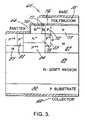
- FIG. 3is an IGBT formed in accordance with this invention and having a P type channel layer in which regions therein are doped to N type conductivity.
- FIG. 4is a simulated doping profile for a MOSFET formed in accordance with this invention.
- FIG. 5is the simulated forward biased collector current response for a MOSFET formed in accordance with this invention.
- FIG. 6is the simulated blocking characteristic profile for a MOSFET formed in accordance with this invention.
- FIG. 7is a simulated representation of transfer characteristics of MOSFETs with N type channel layers of the prior art and P type channel layers formed in accordance with this invention.
- the inventionis a device for controlling electrical conduction across a semiconductor body, particularly useful for metal-oxide-semiconductor field effect transistors (MOSFETs) ( 30 ), insulated gate bipolar transistors (IGBTs) ( 65 ), and other semiconductor devices used in power applications across a wide range of temperatures.
- MOSFETsmetal-oxide-semiconductor field effect transistors
- IGBTsinsulated gate bipolar transistors
- the transistors disclosed hereinincorporate a new P type regrown channel layer ( 46 , 66 ) over the P type well ( 33 , 83 ) that surrounds the transistor source region ( 38 , 78 ).
- transistorsmay include a P type or N type channel, depending upon configuration. Any layer or transistor region described herein may have an opposite doping type as that used here, as the descriptions used in this document are for example only.
- semiconductor devicesuch terminology includes all possible materials, including but not limited to silicon, silicon carbide, Group III nitride compounds, alloys of other semiconductor materials, and the like.
- each embodiment of this inventionutilizes a channel layer that has different doping characteristics from one region of the channel layer to other regions of the same layer.
- the overall layeris referred to herein as the channel layer ( 46 ), but the variously doped regions within the channel layer ( 46 ) are identified by their individual doping characteristics or their function.
- a P type region in the channel layer ( 46 )may be considered simply a P type channel layer region, or more precisely as the threshold voltage regulating region due to the fact that the channel conductivity is determined by that P type portion of the channel layer ( 46 ).
- the doped sections of the channel layer ( 46 )together define a single layer of the device.
- the transistor device ( 35 )controls conduction across a semiconductor body from a source ( 38 ) to a drain or collector ( 42 ).
- the gate contact ( 45 )inverts the P type region ( 58 ) and forms a conductive channel zone ( 50 ) in the device for carriers to flow from the source ( 38 ) through the drift region ( 54 ) to the collector ( 42 ).
- the transistor embodiment of this inventionincludes a regrown channel layer ( 46 ) of which the P type region ( 58 ) forming the channel ( 50 ) is a part.
- Embodiments of this inventioninclude, but are not limited to, MOSFETs, insulated gate bipolar transistors (IGBTs), and MOS controlled thyristors.
- Devices incorporating the regrown channel layer ( 46 ) described hereintypically control electrical conduction across a semiconductor body. Controlled conduction across the semiconductor utilizes carriers from at least one source region ( 38 ) within the semiconductor body having a first conductivity type.
- the transistors ( 30 ) utilizing this inventioninclude at least one well region ( 33 , 34 ) having a second conductivity type and located sufficiently close to the source region ( 38 ) to control the current emanating from the source ( 38 ).
- the drift region ( 54 )is adjacent the side of at least one of the well regions ( 33 , 34 ) and opposite the source region ( 38 ).
- the drift region ( 54 )has the same first conductivity type as the source ( 38 ) for providing a conductive path for carriers from the source region ( 38 ).
- One aspect of this invention that has yet to be shown in prior transistorsis that of a channel layer ( 46 ) having sections ( 56 , 57 , 58 , 60 ) of opposite conductivity type adjacent one another.
- the channel layer ( 46 )extends across the device ( 30 ) and is positioned on at least a portion of the source ( 38 ), well ( 33 , 34 ), and drift regions ( 54 ).
- the channel layer ( 46 )thereby provides a conductive path across the well region ( 33 ) to the drift region ( 54 ).
- the channel layer ( 46 )has a first conductivity type section ( 56 , 57 ) adjacent the source region ( 38 ) and a second conductivity type section ( 58 ) adjacent the well region ( 33 ).
- the transistor ( 30 ) formed according to this inventionincludes a control contact ( 45 ) on the channel layer ( 46 ) for controlling the current from the source ( 38 ) and across the drift region ( 54 ).
- the control contactis a gate contact ( 45 ) that includes a metal layer ( 45 ) atop a layer of polysilicon ( 44 ).
- the gate contact of FIG. 2may be formed by numerous methods that are well known in the art.
- the regrown channel layer ( 46 ) of this inventionmay be formed initially of a semiconductor material having the opposite conductivity type as the source region ( 38 ).
- devices utilizing N type source regions ( 38 )benefit from the epitaxial growth of a P type regrown channel layer ( 46 ).
- devices using P type regrown channel layers ( 46 )exhibit a higher threshold voltage than counterpart devices using the N type regrown channel of the prior art ( FIG. 1 ).
- the higher threshold voltageprovides greater assurance that the device ( 30 ) will be normally off at a gate ( 45 ) bias of zero volts for all operation temperatures. Simulation results have shown that a P type regrown channel layer ( 46 ) yields a threshold voltage increase of more than 1 V at room temperature, a good indication that the device ( 30 ) will be stable in ordinary operating conditions.
- the inventionis a device for controlling conduction across semiconductor layers via a P type epitaxially grown channel layer ( 46 ) with a doping concentration between about 1 ⁇ 10 16 atoms/cm ⁇ 3 and about 5 ⁇ 10 16 atoms/cm ⁇ 3 .
- the P type channel layer ( 46 )may be epitaxially grown on the semiconductor body (e.g., the transistor drift region ( 54 )) with a non-uniform doping concentration across the thickness of the regrown channel layer.
- the non-uniform doping concentrationmay encompass designs in which the regrown channel layer ( 46 ) has a higher doping concentration along the boundary of the drift region ( 54 ) than the doping concentration of that portion of the regrown channel layer ( 46 ) closest to the control, or gate, contact ( 45 ).
- the non-uniform doping concentrationmay have a doping profile that is of any desirable configuration, such as a delta ( ⁇ ) shaped doping profile.
- each region of the deviceis tailored to the use at hand.
- the source ( 38 )is highly doped N type (N++) and the well region has at least one portion that is highly doped P type (P++) ( 34 ).
- the well region surrounding the source regionmay include more than one doping level. For instance, device performance increases when the well region controls conduction from the source with a P+ well ( 33 ) on either side of the source ( 38 ) and a P++ well ( 34 ) below the source ( 38 ).
- the N type source ( 38 )is surrounded by P type well regions of varying but effective doping levels.
- the P+ well regions ( 33 )may be formed using implantation techniques in which the doping profile is generally a box profile with relatively consistent doping from bottom to top.
- the P+ well regions ( 33 )may utilize doping techniques such as “retrograde to the surface” or “buried implantation.”
- the retrograde profileincludes a p-type doping concentration that decreases from the bottom of the well toward the top of the well (i.e., from the portion of the well ( 33 , 83 ) closest to the drift region ( 54 ) toward the portion of the well closest to the regrown channel layer ( 46 )).
- FIGS. 2 and 3show these optional top regions ( 31 , 81 ) of the P+ well beginning at the dotted line therein.
- the devices disclosed hereinutilize either the box profile, buried implantation, or retrograde to surface configurations for the P+ wells ( 33 , 83 ).
- the retrograde profilethat includes decreasing p-type carrier levels from the bottom of the P+ well ( 33 ) toward the top of the P+ well ( 33 )
- the devicehas reduced crystal damage on the surface of the well ( 33 ) because surface implantation has been reduced or even eliminated.
- the retrograde profilefurther thickens the inversion channel region ( 58 ), referred to herein as the P type threshold voltage regulating portion ( 58 ), to include not only region ( 58 ) from the regrown p-type layer but also the top region ( 31 ) of the P+ well ( 33 ).
- This techniquesignificantly reduces the device channel resistance.
- the invention disclosed hereinadds further control features to the regrown channel layer ( 46 ) by dividing the P type regrown channel layer ( 46 ) into sections ( 56 , 57 , 58 , 60 ) of different conductivity types. These variously doped sections of the channel layer ( 46 ) are referred to herein as channel layer regions ( 56 , 57 , 58 , and 60 ). Given the fact that the channel layer ( 46 ) is divided into regions ( 56 , 57 , 58 , and 60 ), the gate contact ( 45 ) voltage inverts only a portion, referred to as the channel zone ( 50 ), of a P type regrown channel layer section ( 58 ) proximate an N type source ( 38 ).
- the N+ source ( 38 )provides carriers for conduction from the source ( 38 ), through N type channel layer regions ( 56 , 57 ) to the channel zone ( 50 ) of the P type channel layer region ( 58 ). At that point, the carriers are swept across the drift region ( 54 ) toward the collector ( 42 ).
- the separately doped channel layer regions ( 56 , 57 , 58 , 60 )add an additional level of control that allows the voltage on the gate ( 45 ) to manipulate accurately the magnitude of the current conducting through the device ( 30 ).
- the channel layer ( 46 )preferably starts with an opposite conductivity type as the source region ( 38 ).
- the channel layer ( 46 )is an epitaxially-grown P type semiconductor layer. Regions of the P type channel layer ( 46 ) are doped to varying levels of N type conductivity to accomplish the voltage control desired for purposes herein.
- the channel layer regionsrange from N++ type ( 56 ) to N type ( 57 ) to P type ( 58 ) and back to N ( 60 ).
- each side of the devicemay have symmetrical doping schemes.
- One design for the channel layer ( 46 )includes divided regions with sufficient doping to form a P type channel layer region ( 58 ) surrounded by N type regions ( 56 , 57 , 60 ) with varying doping levels that can be tailored for the use at hand.
- the P type divided channel layer region ( 58 )provides an additional amount of control to the threshold voltage necessary for carriers to cross the P type channel layer region ( 58 ) and allow conduction through the device.
- the threshold voltagemust be sufficient to invert a portion of the P type channel layer region ( 58 ) and form a conductive channel zone ( 50 ) there through.
- the carriers from the source ( 38 )traverse the channel layer ( 46 ), thereby escaping the wells ( 33 , 34 ).
- the N++ divided channel layer region ( 56 ) and N type channel layer region ( 57 )extend over at least a portion of the source ( 38 ) and provide additional carriers across the conductive channel ( 50 ).
- the overall devices that control currenttypically incorporate layers of semiconductor material that are epitaxially grown on a substrate.
- An exemplary deviceincludes a silicon carbide substrate ( 41 ) with a collector contact ( 42 ) on one side and an epitaxially-formed semiconductor drift region, or drift layer, ( 54 ) on the other side.
- the drift regionmay be of N ⁇ conductivity type.
- the layer on the drift layer ( 54 )includes at least one P++ well region ( 34 ) and at least one P+ well region ( 33 ), both of which at least partially surround an N+ source region ( 38 ) formed by implanting dopants in the semiconductor region on the P++ well region ( 38 ).
- P++ type junction termination wells ( 35 )are located beside the respective well regions on either side of the device ( 30 ).
- the channel layer ( 46 )is positioned on the doped epitaxial layer that includes the source ( 38 ), wells ( 33 , 34 ), and a portion of the drift region ( 54 ). This upper portion of the drift region may be an epitaxial layer ( 61 ) that forms the JFET region of the transistor and is N type conductivity.
- the different portions of the devicemay be doped to any doping range that allows functional control of the conduction from the source ( 38 ) to the collector ( 42 ).
- the device of FIG. 2may have a substrate ( 41 ) doped to N+ type conductivity with a doping level of about 5 ⁇ 10 18 atoms/cm ⁇ 3 .
- the source region ( 38 )is an N+ type source region doped to a level of about 1 ⁇ 10 20 atoms/cm ⁇ 3 .
- the wells ( 33 , 34 ) around the source region ( 38 )include at least one P+ type well section ( 33 ) doped to a level of about 5 ⁇ 10 18 atoms/cm ⁇ 3 and a P++ type well section ( 34 ) doped to a level of about 5 ⁇ 10 19 atoms/cm ⁇ 3 .
- the junction termination wells ( 35 )may be positioned opposite the drift region ( 54 ) such that a portion of the well region is between said source region and the junction termination well.
- the P++ junction termination well ( 35 )is doped to a level of about 1 ⁇ 10 19 cm ⁇ 3 .
- the N++ channel layer region ( 56 )is doped to about 5 ⁇ 10 18 atoms/cm ⁇ 3 ; the N type channel layer region ( 57 ) is doped to about 1 ⁇ 10 16 atoms/cm ⁇ 3 , and the remainder of the P type channel layer, i.e., the threshold voltage regulating region, maintains its original doping level as epitaxially grown within a range of between about 1 ⁇ 10 16 atoms/cm ⁇ 3 and about 5 ⁇ 10 16 atoms/cm ⁇ 3 .
- the new channel layer ( 46 )is incorporated into a MOSFET.
- the MOSFET ( 30 )is formed in a semiconductor body that maintains a normally off, nonconductive status at operating temperature such that conduction from the source region ( 38 ) is minimized until a threshold voltage is applied to the MOSFET. Until the voltage on the control contact, or gate ( 45 ), reaches the threshold voltage, the carriers from the source region ( 38 ) are restrained from conduction by at least one well region ( 33 , 34 ) having an opposite conductivity type as the source region ( 38 ).
- This new MOSFET structureincludes the channel layer ( 46 ) described above to electrically connect the source region ( 38 ) to a conductive region ( 54 ) within the semiconductor body.
- a first channel layer region ( 56 )is positioned within the channel layer ( 46 ) and has the same conductivity type as the source region ( 38 ), though the doping levels of the source and the divided regions may vary as necessary for optimal design and performance.
- This first channel layer region ( 56 )extends across at least a portion of the source region ( 38 ) and is preferably positioned atop the source region ( 38 ).
- the channel layer ( 46 )includes regions ( 56 , 57 , 58 , and 60 ) having varying doping types and doping levels.
- One of these regionsserves as a threshold voltage regulating region ( 58 ), described above as a P type channel layer region.
- the threshold voltage regulating regionis located within the channel layer ( 46 ) and has the opposite conductivity type as the source region ( 38 ) to control the threshold voltage that allows conduction across the channel layer ( 46 ).
- the threshold voltage regulating region ( 58 )is positioned adjacent the first divided channel region ( 56 ) and extends across at least a portion of the well region ( 33 ) that surrounds the source region ( 38 ).
- the channel layer ( 46 )may be an epitaxially grown P type layer, and the various divided regions therein are doped by standard methods to create N and N++ regions as desirable to control conduction through the MOSFET.
- the conductionis ultimately controlled by a gate contact ( 45 ) located on the channel layer with the capability to invert a p type portion ( 58 ) of the channel layer ( 46 ).
- the design parameters described aboveare all available for incorporating into the MOSFET. These parameters such as doping type, doping level, doping profile, positions of particular regions, and other factors will not be repeated but are incorporated herein as if fully set forth again.
- the terms “P type channel layer region” and “threshold voltage regulating region”are equivalents and are shown in FIG. 2 as the P type region ( 58 ) of the channel layer ( 46 ).
- the overall inventionis useful in forming a MOSFET ( 30 ) that will reliably remain in the nonconductive state until a threshold voltage is applied to the gate ( 45 ).
- the MOSFETis particularly adept at providing a controlled current at a threshold voltage (and no current below the threshold voltage) for operating temperatures ranging from ⁇ 50° C. to 200° C. This is due in part to having a P type channel layer ( 46 ) epitaxially grown over at least portions of both (i) a source region ( 38 ) and (ii) a well region ( 33 , 34 ) that at least partially surrounds the source region ( 38 ).
- a first channel layer region ( 56 )is positioned within the channel layer and covers at least a portion of the source region ( 38 ).
- This first channel layer region ( 56 )is sufficiently doped so that the first channel layer region ( 56 ) is N type.
- a threshold voltage regulating regiondescribed above as the P type channel layer region ( 58 ), is positioned within the channel layer ( 46 ) adjacent the first channel region ( 56 ) and extending over at least a portion of the well region ( 33 ), said threshold voltage regulating region ( 58 ) having P type conductivity to control the threshold voltage necessary to allow conduction from the source region ( 38 ) across the well region ( 33 ).
- the MOSFET of this inventionincludes a control contact, or gate ( 45 ) on the channel layer ( 46 ) for controlling the current from the source across the well region.
- an insulated gate bipolar transistor (IGBT) ( 65 )may have a controlled threshold voltage by incorporating a channel layer ( 66 ) therein with sections ( 70 , 71 , 72 , 73 ) of different doping characteristics.
- the IGBT ( 65 ) of this inventionincludes an emitter region ( 78 ) of a first conductivity type at least partially surrounded by a base region ( 83 , 84 ) of opposite conductivity type, wherein the emitter region ( 78 ) is positioned between the channel layer ( 66 ) and the base region ( 83 , 84 ).
- the IGBT ( 65 )further includes a base contact ( 85 ) on the channel layer ( 66 ), wherein the gate contact ( 85 ) extends across the length of at least a portion of both the emitter ( 78 ) and base ( 83 , 84 ) regions for controlling conduction through at least one p-n junction between the base region ( 83 , 84 ) and a collector ( 82 ).
- the IGBTmay be formed on a substrate ( 90 ) of P type conductivity to support an N ⁇ type drift region ( 89 ) under a JFET region ( 87 ) of N type conductivity.
- the JFET region ( 89 )may be an epitaxial layer formed on the drift region during the manufacturing process.
- the IGBTis further characterized by having a divided channel layer that incorporates sections, or regions ( 70 , 71 , 72 , 73 ), of varying doping characteristics.
- a first IGBT channel layer region ( 70 )is positioned within the channel layer ( 66 ) and has the same conductivity type as the emitter region ( 78 ).
- the first channel layer region ( 70 )extends across at least a portion of the emitter region ( 78 );
- a threshold voltage regulating region ( 72 )is also positioned within the channel layer ( 66 ) and has the opposite conductivity type as the emitter region ( 78 ).
- the threshold voltage regulating region ( 72 )is preferably adjacent the first channel layer region ( 70 ) and extends across at least a portion of the base region ( 83 ).
- the threshold voltage regulating regionincreases the threshold voltage on the gate that is necessary to allow conduction from the source region toward the IGBT collector ( 82 ).
- the method of forming the devicesfurther exemplifies the unique nature of this invention.
- the method hereincludes forming semiconductor devices having controlled threshold voltage levels allowing conduction from a source region ( 38 , 78 ), across a well region ( 33 , 83 ), to a drift region ( 54 , 89 ) within the body of the semiconductor device.
- the methodincludes the steps of (i) implanting at least one P type well ( 33 , 34 , 83 , 84 ) into an N type, or N ⁇ type, semiconductor body to depths that define at least one N type source region ( 38 , 78 ) at least partially surrounded by the P type well ( 33 , 34 , 83 , 84 ); (ii) doping the N type source region ( 38 , 78 ) to form an N+ type source region ( 38 , 78 ); (iii) growing a P type channel layer ( 46 , 66 ) over at least a portion of both said well and said source region; (iv) doping sections of said P type channel layer ( 46 , 66 ) to convert the sections to N type channel layer regions ( 56 , 57 , 58 , 60 , 70 - 73 ), said N type channel layer regions abutting opposite sides of at least one P type section ( 58 , 72 ) of the originally P type regrown channel layer ( 46 ,
- the methodmay include forming an N type epitaxial JFET region ( 61 , 87 ) adjacent the source region.
- the method of this inventionavoids certain pitfalls resulting from process steps of the prior art.
- the previously known processes for forming an N type channel layeryields carrier scattering within layers of the device, and these scattered carriers affect the threshold voltage that turns on the device for conduction, i.e., the scattered carriers lower the threshold voltage and allow undesirable conduction.
- the scatteringoccurs during device fabrication steps including, but not limited to, the doping procedures, steps that vary layer thickness, misalignment in defining the channel region, or activation temperature floating, etc.
- the P type regrown channel layer ( FIG. 2 , No. 46 ) of this inventionyields significantly less scattering and minimizes the detrimental effect on the threshold voltage, potentially enhancing device yields for mass production.
- the method disclosed herein for fabricating a regrown channel layer of P type semiconductor materialwould also be compatible for forming conventional DMOSFETs.
- the method of this inventionhas the added benefit of defining the channel length solely by the features of the photo mask instead of buffered oxide etching (“BOE wet etching”) used in self-alignment DMOSFET fabrication processes. This advantage can significantly ensure repeatability of the device performance and is significant for mass production.
- BOE wet etchingbuffered oxide etching
- FIG. 4is a graphical representation of the doped semiconductor MOSFET similar to that which could be manufactured for use.
- the doping typeswould correspond to the above noted descriptions for FIG. 1 with the doping levels noted in the legend of FIG. 4 .
- transistors with the P type regrown channel layer having varied doping profilesshow a well-controlled drain current across a wide spectrum of gate and substrate voltages.
- FIG. 6shows that the current response in the device formed with the P type channel of this invention is consistent at operating temperature even when the substrate voltage ranges from 0 to 1200 volts.
- a transistor having an N type re-grown channel layer of the prior artrapidly loses control of its current response regardless of gate voltage.
- FIG. 7is particularly telling in that a transistor having the P type regrown channel layer set forth above can achieve a threshold voltage that is about 1 volt higher than the N type channel layer of the prior art at the same operating temperature.
- the threshold voltagedepends upon the channel layer doping level as shown in FIG. 7 .
Landscapes
- Insulated Gate Type Field-Effect Transistor (AREA)
- Metal-Oxide And Bipolar Metal-Oxide Semiconductor Integrated Circuits (AREA)
Abstract
Description
- The invention relates to the field of semiconductor transistors utilizing a voltage applied to a gate contact to control current in a conductive channel. The device disclosed herein is particularly useful in the art of power transistors that operate in a wide range of temperatures. Transistors formed by the new method include a regrown P type epitaxial layer for the channel layer and thus exhibit better control at room temperature or even elevated temperatures.
- Numerous efforts have been underway to develop silicon carbide MOSFETs using conventional DMOS (double diffused metal-oxide-semiconductor) structures with an N type regrown channel that improves channel mobility. The presence of the N type regrown channel causes inherent fluctuations in device performance because the threshold voltage shifts with operating conditions. Research shows that the varying threshold voltage results, at least in part, from scattered carriers distributed through the device during manufacturing steps, such as during channel layer regrowth, N type ion implantation, dopant activation, etc. In general, the N type regrown layer reduces the threshold voltage by about 1 volt as compared to standard transistors with no regrown channel layer. This change in threshold voltage leads to undesirable variations in conduction at both room temperature and elevated temperatures.
- The innovative features of this invention are useful in several different semiconductor devices and are particularly effective in MOSFET designs. Commonly assigned U.S. Pat. No. 6,956,238 (Ryu 2005) sets forth a significant list of literature describing the history, structure, and performance characteristics of power MOSFETS. The Ryu '238 patent is incorporated by reference as if fully set forth herein. Generally, power MOSFETs utilize a gate contact to control conductivity in the semiconductor channel of the device. When the voltage on the gate is sufficiently high, the transistor will conduct large currents from source to drain so long as the appropriate inversion layer allows carriers from the source to cross into the drift region of the device.
- Numerous efforts have been taken to develop SiC MOSFETs using conventional techniques, such as double diffusion.
FIG. 1 shows an example. These appropriately named DMOSFETs (double diffused metal oxide semiconductor field effect transistors) include P type wells (12,14) surrounding an N type source (16,17) (or the opposite conductivity types depending on the type of device). For current to flow from source (16,17) to drain (20) across a drift region (22), the traditional DMOSFETs (10) require a sufficient voltage on the gate contact (24) atop an oxide layer (26) to invert a channel region (28) in the P type well (12,14) so that N type carriers from the source (16,17) can traverse the wells (12,14), cross the conductive drift region (22), and form a large current on the drain contact (20). See Prior Art FIG. 1. - As set forth in the Ryu '238 patent of the prior art, the p-wells of a DMOSFET are semiconductor regions implanted with aluminum or boron, and the source region is implanted with nitrogen or phosphorus. The implants are activated at temperatures between 1400° C. to 1700° C. The contacts to N+ layers are annealed layers of nickel (Ni) while the contacts to the P+ regions of the device would be nickel (Ni), titanium (Ti), or an alloy of titanium and aluminum (Ti/Al). A dielectric layer, such as silicon nitride or silicon dioxide, separates the gate contact from the semiconductor layer of the transistor. See U.S. Pat. No. 6,956,238 (Ryu, 2005) (Col. 2, Lines 44-55). Ryu notes (col. 2, lines 58-65) that one problem with DMOSFETs is poor mobility in the inversion layer, leading to very high on-resistance.
- Ryu '238 previously alleviated this high on-resistance to a certain extent by forming a thin layer of silicon carbide over the well regions surrounding the source. This thin layer (26) is doped to N type conductivity with nitrogen or phosphorus and extends from the source region to the drift region. The thin semiconductor layer (26) provides a shorting channel for carriers from the source to traverse the well region, thereby enhancing conduction from source to drain. See Ryu '238 (col. 11, lines 33-38). In a different embodiment, Ryu utilizes a regrown epitaxial layer that is grown over the P type wells and extends across the drift region. See Ryu '238 (col. 12, lines 8-36). In this embodiment of Ryu's device, the regrown silicon carbide layer is undoped.
- Ryu's silicon carbide regrown layer has a thickness from about 0.05 microns to about 1 micron, but a thinner layer of between about 1000 and 5000 angstroms is preferred. According to Ryu, the thin, N type shorting channels and regrown layers self deplete the channel at zero bias to prevent unwanted conduction in the off state. These layers also provide a low resistance route for source carriers to aid the inversion layer in providing conduction to the drain. Furthermore, the regrown layer reduces the surface roughness created by implant activation annealing. In this regard, the conductive channel is positioned in the epitaxial layer for better conductivity. See Ryu '238, col. 12, lines 30-35.
- Ryu has achieved considerable advancement in controlling the zero bias state and preventing conductivity at that point while also providing a low on-resistance under forward biasing. Still, however, the presence of the N type regrown channel layer (26) causes fluctuation in the threshold voltage that turns on the device, partly because temperature variations affect channel depletion in the shorting channels and regrown layer. Interface states and electron scattering, natural results of Ryu's ion implantation and activation, further complicate the unpredictable threshold voltage in devices with Ryu's regrown layer. In fact, an N type regrown layer may reduce threshold voltage by as much as 1 V as compared to devices with no regrown layer. Accordingly, devices with an N type regrown layer may exhibit unwanted forward conduction at room temperature or other operating temperatures, even at zero gate bias.
- Attempts to control threshold voltage, even in devices used at various operating temperatures, have previously manipulated the structural features of the conductive channel. For instance, U.S. Pat. No. 5,905,284 (Fuji, 1999) discusses the fact that as gate oxide films between the gate and the transistor body become increasingly thinner with device miniaturization, the gate impurities diffuse into the channel, causing unwanted conduction at zero gate bias. (Fuji, col. 2, lines 17-22). Fuji notes that one remedy to this problem may be found in forming the gate oxide films and gate contacts discretely, which, of course leads to higher manufacturing costs. Fuji then suggests a method of forming the diffusively doped regions in the transistor in defined layers with varying annealing temperatures and different angles of dopant implantation. (col. 4, lines 28-40; col. 13, lines 1-15).
- In a different technique for ensuring the integrity of a device threshold voltage at operating temperatures, Han et al. show that the doping profile of the source is another way to manage conductivity in the channel. See EP 0744769 A2 (col. 10, lines 3-29). In Han's FIG. 5, as the phosphorus concentration in the channel decreases, the latch current density steadily increases, but the latch does not occur when the phosphorus doping is less than 5×1018cm−3. All the while, forward current density decreases only slightly, further adding to Han's positive result. For general purposes, Han shows that as the phosphorus concentration decreases along the surface of the source, the size of the source is reduced vertically in Han's FIG. 1, so the length of the channel is increased. The P+ polarity in the channel is also increased, thereby maintaining a higher than expected threshold voltage. See Han '769 (col. 10, lines 25-30).
- Even with Ryu's advances in increasing channel efficiency with regrown N type layers and other efforts in this area, a need still exists in the art of power electronics for a transistor with high conductivity in the channel without the corresponding deterioration in threshold voltage. Other attempts to manage the threshold voltage characteristics of power transistors require manipulating the source to an extent that maximum conductivity cannot be achieved. Accordingly, there exists a persistent need in the art for a power transistor with low on resistance, high channel conductivity, and a reliable threshold voltage even at a wide range of operating temperatures.
- The invention is a device for controlling electrical conduction across a semiconductor body having a P type channel layer that is divided into sections, or regions, of varying conductivity type and doping level. The device, often a MOSFET (30) or an IGBT (65), includes at least one source region (38,78) within the semiconductor body, the source region (38,78) having a first conductivity type. The source region is surrounded by at least one well region (33,34,83,84) having a second conductivity type to control carrier flow from the source region to a collector (42,82). A drift region (54,89) provides a conductive path adjacent the side of the well region (33,34,83,84) opposite the source region (38,78), the drift region (54,89) having the first conductivity type, typically of a lower doping level N−. The P type channel layer (46,66), as set forth in this invention, is positioned on at least a portion of the source, well, and drift regions, to provide a conductive path across the well region to the drift region. As noted herein, the channel layer (46,66) has a region, or divided section (56,57,58,60,70-73), of a first conductivity type adjacent the source region and a region, or section, of the second conductivity type adjacent the well region. A control contact (45,85) on the channel layer (46,66) regulates the current from the source across the drift region to the drain, or collector contact (42,82).
- A MOSFET formed in accordance with this invention includes a semiconductor body that maintains a normally off status at operating temperature such that conduction from the source region (38) is minimized until a threshold voltage is applied to the MOSFET. Up to the point of reaching a desired threshold voltage applied to the gate, the carriers from the source region are restrained from conduction by at least one well region (33,34) having an opposite conductivity type as the source region (38). The well region (33) closest to the channel layer may have a retrograde doping profile such that the conductivity decreases from bottom to top. This doping type forms a retrograde layer (31) closest to the channel layer (46). It follows then, that according to one embodiment of this invention, the MOSFET includes a channel layer (46) formed on the MOSFET semiconductor body to electrically connect the source region (38) to a conductive drift region (54) within the semiconductor body.
- The channel layer (46) in the claimed MOSFET includes a first channel layer region (56) positioned within the channel layer (46) and having the same conductivity type as the source region (38). The first channel layer region (56) extends across at least a portion of the source region (38). A threshold voltage regulating region (58) within the channel layer (46) and proximate the first channel layer region (56), has the opposite conductivity type as the source region (38) to control the threshold voltage that allows conduction across the channel layer (46). The threshold voltage regulating region (58) is positioned proximate the first channel layer region (56) and extends across at least a portion of the well region (33). A control contact (45) on the channel layer (46) controls current flowing from the source region through the channel layer.
- The P type channel layer (46,66) of this invention may be positioned between two different components of the device: (i) the layer incorporating source (38,78) and drift regions (54,89) and (ii) the insulator material (52,76) supporting the gate contact (45,85). By dividing the channel layer (46,66) into sections, or regions, the channel layer (46,66) allows better control over the threshold voltage that regulates current from source to drain or, similarly, from emitter to collector. Accordingly, one of the channel layer regions in the claimed channel layer of this invention is a threshold voltage regulating region (58,72).
- The P type channel layer (46,66) may be incorporated into a number of transistors and other semiconductor devices in which current control is desirable. The invention, therefore, includes a method of forming a semiconductor device that has the P type channel layer (46,66) with sections, or regions (56,57,58,60,70-73), therein that have been doped to N type conductivity. The method includes the steps of (i) implanting at least one P type well (33,34,83,84) into an N type semiconductor body to depths that define at least one N type source region (38,78) at least partially surrounded by the P type well (33,34,83,84); (ii) doping the N type source region (38,78) to form an N+ type source region; (iii) growing a P type channel layer (46,66) over at least a portion of both said well and said source region; (iv) doping sections of said P type channel layer to convert the sections to N type channel layer regions, said N type channel layer regions abutting opposite sides of at least one P type section of said channel layer; and (v) forming a gate contact (45,85) on the channel layer, the gate contact at lease partially covering at least one N type channel layer region and at least one P type channel layer region. These steps, enumerated here only for clarity, may be accomplished in other orders, with intervening steps for added efficiencies, and may utilize common techniques available for processing semiconductor materials.
FIG. 1 is a prior art MOSFET having an N type channel layer.FIG. 2 is a MOSFET formed in accordance with this invention and having a P type channel layer in which regions therein are doped to N type conductivity.FIG. 3 is an IGBT formed in accordance with this invention and having a P type channel layer in which regions therein are doped to N type conductivity.FIG. 4 is a simulated doping profile for a MOSFET formed in accordance with this invention.FIG. 5 is the simulated forward biased collector current response for a MOSFET formed in accordance with this invention.FIG. 6 is the simulated blocking characteristic profile for a MOSFET formed in accordance with this invention.FIG. 7 is a simulated representation of transfer characteristics of MOSFETs with N type channel layers of the prior art and P type channel layers formed in accordance with this invention.- The invention is a device for controlling electrical conduction across a semiconductor body, particularly useful for metal-oxide-semiconductor field effect transistors (MOSFETs) (30), insulated gate bipolar transistors (IGBTs) (65), and other semiconductor devices used in power applications across a wide range of temperatures. The transistors disclosed herein incorporate a new P type regrown channel layer (46,66) over the P type well (33,83) that surrounds the transistor source region (38,78).
- This detailed description should not limit the invention to literal terms. For example, terms describing relative position of elements in this invention should be given their broadest meaning unless otherwise noted. For example, when a transistor element or layer is located “on” another layer, “beside” another element, or “adjacent” or “proximate” a certain part of the device at hand, that terminology suggests that intervening parts of the device may be present between the recited elements if necessary. When a layer is “directly adjacent” or “directly beside” another element, the term typically indicates that there are no intervening elements there between.
- Those having skill in the art will recognize that the invention may be embodied in many different types of transistors device structures. Accordingly, the invention is not limited to the particular structures illustrated herein. For example, transistors may include a P type or N type channel, depending upon configuration. Any layer or transistor region described herein may have an opposite doping type as that used here, as the descriptions used in this document are for example only. When the device is described as a “semiconductor device,” such terminology includes all possible materials, including but not limited to silicon, silicon carbide, Group III nitride compounds, alloys of other semiconductor materials, and the like.
- As noted above, each embodiment of this invention utilizes a channel layer that has different doping characteristics from one region of the channel layer to other regions of the same layer. The overall layer is referred to herein as the channel layer (46), but the variously doped regions within the channel layer (46) are identified by their individual doping characteristics or their function. For example, a P type region in the channel layer (46) may be considered simply a P type channel layer region, or more precisely as the threshold voltage regulating region due to the fact that the channel conductivity is determined by that P type portion of the channel layer (46). In any event, the doped sections of the channel layer (46) together define a single layer of the device.
- In a first embodiment, the transistor device (35) controls conduction across a semiconductor body from a source (38) to a drain or collector (42). The gate contact (45) inverts the P type region (58) and forms a conductive channel zone (50) in the device for carriers to flow from the source (38) through the drift region (54) to the collector (42). The transistor embodiment of this invention includes a regrown channel layer (46) of which the P type region (58) forming the channel (50) is a part. Embodiments of this invention include, but are not limited to, MOSFETs, insulated gate bipolar transistors (IGBTs), and MOS controlled thyristors.
- Devices incorporating the regrown channel layer (46) described herein typically control electrical conduction across a semiconductor body. Controlled conduction across the semiconductor utilizes carriers from at least one source region (38) within the semiconductor body having a first conductivity type. To ensure a proper threshold voltage to regulate conduction for various applications, the transistors (30) utilizing this invention include at least one well region (33,34) having a second conductivity type and located sufficiently close to the source region (38) to control the current emanating from the source (38). The drift region (54) is adjacent the side of at least one of the well regions (33,34) and opposite the source region (38). The drift region (54) has the same first conductivity type as the source (38) for providing a conductive path for carriers from the source region (38).
- One aspect of this invention that has yet to be shown in prior transistors is that of a channel layer (46) having sections (56,57,58,60) of opposite conductivity type adjacent one another. The channel layer (46) extends across the device (30) and is positioned on at least a portion of the source (38), well (33,34), and drift regions (54). The channel layer (46) thereby provides a conductive path across the well region (33) to the drift region (54). As shown in
FIG. 2 , the channel layer (46) has a first conductivity type section (56,57) adjacent the source region (38) and a second conductivity type section (58) adjacent the well region (33). - In certain commonly used embodiments, the transistor (30) formed according to this invention includes a control contact (45) on the channel layer (46) for controlling the current from the source (38) and across the drift region (54). In the MOSFET of
FIG. 2 , the control contact is a gate contact (45) that includes a metal layer (45) atop a layer of polysilicon (44). The gate contact ofFIG. 2 may be formed by numerous methods that are well known in the art. - Unlike regrown channel layers of the prior art discussed above (
FIG. 1 ), the regrown channel layer (46) of this invention may be formed initially of a semiconductor material having the opposite conductivity type as the source region (38). For example, and without limiting the scope of the invention herein, devices utilizing N type source regions (38) benefit from the epitaxial growth of a P type regrown channel layer (46). In general, devices using P type regrown channel layers (46) exhibit a higher threshold voltage than counterpart devices using the N type regrown channel of the prior art (FIG. 1 ). The higher threshold voltage provides greater assurance that the device (30) will be normally off at a gate (45) bias of zero volts for all operation temperatures. Simulation results have shown that a P type regrown channel layer (46) yields a threshold voltage increase of more than 1 V at room temperature, a good indication that the device (30) will be stable in ordinary operating conditions. - In one embodiment, therefore, the invention is a device for controlling conduction across semiconductor layers via a P type epitaxially grown channel layer (46) with a doping concentration between about 1×10¹⁶atoms/cm−3and about 5×10¹⁶atoms/cm−3. The P type channel layer (46) may be epitaxially grown on the semiconductor body (e.g., the transistor drift region (54)) with a non-uniform doping concentration across the thickness of the regrown channel layer. The non-uniform doping concentration may encompass designs in which the regrown channel layer (46) has a higher doping concentration along the boundary of the drift region (54) than the doping concentration of that portion of the regrown channel layer (46) closest to the control, or gate, contact (45). The non-uniform doping concentration may have a doping profile that is of any desirable configuration, such as a delta (δ) shaped doping profile.
- The doping level of each region of the device is tailored to the use at hand. In a preferred embodiment, the source (38) is highly doped N type (N++) and the well region has at least one portion that is highly doped P type (P++) (34). The well region surrounding the source region may include more than one doping level. For instance, device performance increases when the well region controls conduction from the source with a P+ well (33) on either side of the source (38) and a P++ well (34) below the source (38). In this embodiment, the N type source (38) is surrounded by P type well regions of varying but effective doping levels.
- The P+ well regions (33) may be formed using implantation techniques in which the doping profile is generally a box profile with relatively consistent doping from bottom to top. In an additional embodiment, the P+ well regions (33) may utilize doping techniques such as “retrograde to the surface” or “buried implantation.” In this embodiment, the retrograde profile includes a p-type doping concentration that decreases from the bottom of the well toward the top of the well (i.e., from the portion of the well (33,83) closest to the drift region (54) toward the portion of the well closest to the regrown channel layer (46)). With the P+ well (33) doping characterized by a retrograde profile, it is possible that the top region (31) of the P+ well (33) will actually be of n-type conductivity.
FIGS. 2 and 3 show these optional top regions (31,81) of the P+ well beginning at the dotted line therein. - It is within the scope of the devices disclosed herein to utilize either the box profile, buried implantation, or retrograde to surface configurations for the P+ wells (33,83). By using the retrograde profile that includes decreasing p-type carrier levels from the bottom of the P+ well (33) toward the top of the P+ well (33), the device has reduced crystal damage on the surface of the well (33) because surface implantation has been reduced or even eliminated. The retrograde profile further thickens the inversion channel region (58), referred to herein as the P type threshold voltage regulating portion (58), to include not only region (58) from the regrown p-type layer but also the top region (31) of the P+ well (33). The same is true for the IGBT embodiment of
FIG. 3 . This technique significantly reduces the device channel resistance. - The invention disclosed herein adds further control features to the regrown channel layer (46) by dividing the P type regrown channel layer (46) into sections (56,57,58,60) of different conductivity types. These variously doped sections of the channel layer (46) are referred to herein as channel layer regions (56,57,58, and60). Given the fact that the channel layer (46) is divided into regions (56,57,58, and60), the gate contact (45) voltage inverts only a portion, referred to as the channel zone (50), of a P type regrown channel layer section (58) proximate an N type source (38). In the channel layer (46) of
FIG. 2 , the N+ source (38) provides carriers for conduction from the source (38), through N type channel layer regions (56,57) to the channel zone (50) of the P type channel layer region (58). At that point, the carriers are swept across the drift region (54) toward the collector (42). - The separately doped channel layer regions (56,57,58,60) add an additional level of control that allows the voltage on the gate (45) to manipulate accurately the magnitude of the current conducting through the device (30). As described above, the channel layer (46) preferably starts with an opposite conductivity type as the source region (38). In the device of
FIG. 2 , the channel layer (46) is an epitaxially-grown P type semiconductor layer. Regions of the P type channel layer (46) are doped to varying levels of N type conductivity to accomplish the voltage control desired for purposes herein. InFIG. 2 , the channel layer regions range from N++ type (56) to N type (57) to P type (58) and back to N (60). As shown inFIG. 2 , each side of the device may have symmetrical doping schemes. One design for the channel layer (46) includes divided regions with sufficient doping to form a P type channel layer region (58) surrounded by N type regions (56,57,60) with varying doping levels that can be tailored for the use at hand. The P type divided channel layer region (58) provides an additional amount of control to the threshold voltage necessary for carriers to cross the P type channel layer region (58) and allow conduction through the device. The threshold voltage must be sufficient to invert a portion of the P type channel layer region (58) and form a conductive channel zone (50) there through. Upon establishment of a conductive channel zone (50), the carriers from the source (38) traverse the channel layer (46), thereby escaping the wells (33,34). The N++ divided channel layer region (56) and N type channel layer region (57) extend over at least a portion of the source (38) and provide additional carriers across the conductive channel (50). - Additional design details may be incorporated into the device (30) of
FIG. 2 depending upon the use at hand. Without limiting the invention or the devices that may incorporate any part of the invention, the overall devices that control current typically incorporate layers of semiconductor material that are epitaxially grown on a substrate. An exemplary device includes a silicon carbide substrate (41) with a collector contact (42) on one side and an epitaxially-formed semiconductor drift region, or drift layer, (54) on the other side. The drift region may be of N− conductivity type. By implanting P type dopants, the layer on the drift layer (54) includes at least one P++ well region (34) and at least one P+ well region (33), both of which at least partially surround an N+ source region (38) formed by implanting dopants in the semiconductor region on the P++ well region (38). P++ type junction termination wells (35) are located beside the respective well regions on either side of the device (30). The channel layer (46) is positioned on the doped epitaxial layer that includes the source (38), wells (33,34), and a portion of the drift region (54). This upper portion of the drift region may be an epitaxial layer (61) that forms the JFET region of the transistor and is N type conductivity. A gate insulator (52), such as silicon dioxide or other passivating material, covers the channel layer (46) and forms a region on which the gate contact (45) may be formed. - As is often used in technology of the type, the different portions of the device may be doped to any doping range that allows functional control of the conduction from the source (38) to the collector (42). For example only, and without limiting the doping ranges that may be used, the device of
FIG. 2 may have a substrate (41) doped to N+ type conductivity with a doping level of about 5×10¹⁸atoms/cm−3. The source region (38) is an N+ type source region doped to a level of about 1×10²⁰atoms/cm−3. The wells (33,34) around the source region (38) include at least one P+ type well section (33) doped to a level of about 5×10¹⁸atoms/cm−3and a P++ type well section (34) doped to a level of about 5×10¹⁹atoms/cm−3. The junction termination wells (35) may be positioned opposite the drift region (54) such that a portion of the well region is between said source region and the junction termination well. The P++ junction termination well (35) is doped to a level of about 1×1019cm−3. - The N++ channel layer region (56) is doped to about 5×10¹⁸atoms/cm−3; the N type channel layer region (57) is doped to about 1×10¹⁶atoms/cm−3, and the remainder of the P type channel layer, i.e., the threshold voltage regulating region, maintains its original doping level as epitaxially grown within a range of between about 1×10¹⁶atoms/cm−3and about 5×10¹⁶atoms/cm−3.
- As noted above, it is within the scope of this invention for the new channel layer (46) to be incorporated into a MOSFET. The MOSFET (30) is formed in a semiconductor body that maintains a normally off, nonconductive status at operating temperature such that conduction from the source region (38) is minimized until a threshold voltage is applied to the MOSFET. Until the voltage on the control contact, or gate (45), reaches the threshold voltage, the carriers from the source region (38) are restrained from conduction by at least one well region (33,34) having an opposite conductivity type as the source region (38). This new MOSFET structure includes the channel layer (46) described above to electrically connect the source region (38) to a conductive region (54) within the semiconductor body. A first channel layer region (56) is positioned within the channel layer (46) and has the same conductivity type as the source region (38), though the doping levels of the source and the divided regions may vary as necessary for optimal design and performance. This first channel layer region (56) extends across at least a portion of the source region (38) and is preferably positioned atop the source region (38).
- One aspect of the invention herein is that the channel layer (46) includes regions (56,57,58, and60) having varying doping types and doping levels. One of these regions serves as a threshold voltage regulating region (58), described above as a P type channel layer region. The threshold voltage regulating region is located within the channel layer (46) and has the opposite conductivity type as the source region (38) to control the threshold voltage that allows conduction across the channel layer (46). The threshold voltage regulating region (58) is positioned adjacent the first divided channel region (56) and extends across at least a portion of the well region (33) that surrounds the source region (38).
- It is important to recall that the channel layer (46) may be an epitaxially grown P type layer, and the various divided regions therein are doped by standard methods to create N and N++ regions as desirable to control conduction through the MOSFET. The conduction is ultimately controlled by a gate contact (45) located on the channel layer with the capability to invert a p type portion (58) of the channel layer (46).
- In forming a MOSFET according to this invention, the design parameters described above are all available for incorporating into the MOSFET. These parameters such as doping type, doping level, doping profile, positions of particular regions, and other factors will not be repeated but are incorporated herein as if fully set forth again. For convenience, the terms “P type channel layer region” and “threshold voltage regulating region” are equivalents and are shown in
FIG. 2 as the P type region (58) of the channel layer (46). - The overall invention is useful in forming a MOSFET (30) that will reliably remain in the nonconductive state until a threshold voltage is applied to the gate (45). The MOSFET is particularly adept at providing a controlled current at a threshold voltage (and no current below the threshold voltage) for operating temperatures ranging from −50° C. to 200° C. This is due in part to having a P type channel layer (46) epitaxially grown over at least portions of both (i) a source region (38) and (ii) a well region (33,34) that at least partially surrounds the source region (38). As noted previously, a first channel layer region (56) is positioned within the channel layer and covers at least a portion of the source region (38). This first channel layer region (56) is sufficiently doped so that the first channel layer region (56) is N type. A threshold voltage regulating region, described above as the P type channel layer region (58), is positioned within the channel layer (46) adjacent the first channel region (56) and extending over at least a portion of the well region (33), said threshold voltage regulating region (58) having P type conductivity to control the threshold voltage necessary to allow conduction from the source region (38) across the well region (33). As is typical in functional transistors, the MOSFET of this invention includes a control contact, or gate (45) on the channel layer (46) for controlling the current from the source across the well region.
- Other devices also benefit from the channel layer (46) as set forth herein. As shown in
FIG. 3 , for example, an insulated gate bipolar transistor (IGBT) (65) may have a controlled threshold voltage by incorporating a channel layer (66) therein with sections (70,71,72,73) of different doping characteristics. The IGBT (65) of this invention includes an emitter region (78) of a first conductivity type at least partially surrounded by a base region (83,84) of opposite conductivity type, wherein the emitter region (78) is positioned between the channel layer (66) and the base region (83,84). The IGBT (65) further includes a base contact (85) on the channel layer (66), wherein the gate contact (85) extends across the length of at least a portion of both the emitter (78) and base (83,84) regions for controlling conduction through at least one p-n junction between the base region (83,84) and a collector (82). The IGBT may be formed on a substrate (90) of P type conductivity to support an N− type drift region (89) under a JFET region (87) of N type conductivity. The JFET region (89) may be an epitaxial layer formed on the drift region during the manufacturing process. - The IGBT is further characterized by having a divided channel layer that incorporates sections, or regions (70,71,72,73), of varying doping characteristics. In one embodiment, a first IGBT channel layer region (70) is positioned within the channel layer (66) and has the same conductivity type as the emitter region (78). The first channel layer region (70) extends across at least a portion of the emitter region (78); a threshold voltage regulating region (72) is also positioned within the channel layer (66) and has the opposite conductivity type as the emitter region (78). The threshold voltage regulating region (72) is preferably adjacent the first channel layer region (70) and extends across at least a portion of the base region (83). The threshold voltage regulating region increases the threshold voltage on the gate that is necessary to allow conduction from the source region toward the IGBT collector (82).
- In addition to the device, or apparatus, embodiments described above, the method of forming the devices further exemplifies the unique nature of this invention. The method here includes forming semiconductor devices having controlled threshold voltage levels allowing conduction from a source region (38,78), across a well region (33,83), to a drift region (54,89) within the body of the semiconductor device. The method includes the steps of (i) implanting at least one P type well (33,34,83,84) into an N type, or N− type, semiconductor body to depths that define at least one N type source region (38,78) at least partially surrounded by the P type well (33,34,83,84); (ii) doping the N type source region (38,78) to form an N+ type source region (38,78); (iii) growing a P type channel layer (46,66) over at least a portion of both said well and said source region; (iv) doping sections of said P type channel layer (46,66) to convert the sections to N type channel layer regions (56,57,58,60,70-73), said N type channel layer regions abutting opposite sides of at least one P type section (58,72) of the originally P type regrown channel layer (46,66); and (v) forming a gate contact (45,85) on the channel layer (46,66), the gate contact at lease partially covering at least one N type channel layer region and at least one P type channel layer region. Additionally, the method may include forming an N type epitaxial JFET region (61,87) adjacent the source region. These steps, enumerated here only for clarity, may be accomplished in other orders, with intervening steps for added efficiencies, and may utilize common techniques available for processing semiconductor materials.
- The method of this invention avoids certain pitfalls resulting from process steps of the prior art. The previously known processes for forming an N type channel layer yields carrier scattering within layers of the device, and these scattered carriers affect the threshold voltage that turns on the device for conduction, i.e., the scattered carriers lower the threshold voltage and allow undesirable conduction. The scattering occurs during device fabrication steps including, but not limited to, the doping procedures, steps that vary layer thickness, misalignment in defining the channel region, or activation temperature floating, etc. The P type regrown channel layer (
FIG. 2 , No.46) of this invention yields significantly less scattering and minimizes the detrimental effect on the threshold voltage, potentially enhancing device yields for mass production. - Other benefits are also evident in using a P type regrown layer (46) for forming the channel in a transistor. For example, simulation results have shown that the proposed MOSFETs with a P type regrown channel layer exhibit a much lower reverse leakage current than MOSFETs with an N type regrown channel.
- The method disclosed herein for fabricating a regrown channel layer of P type semiconductor material would also be compatible for forming conventional DMOSFETs. The method of this invention, however, has the added benefit of defining the channel length solely by the features of the photo mask instead of buffered oxide etching (“BOE wet etching”) used in self-alignment DMOSFET fabrication processes. This advantage can significantly ensure repeatability of the device performance and is significant for mass production.
- Simulated testing shows transistors formed in accordance with this invention include highly controlled current responses at a wide range of voltages and temperatures.
FIG. 4 is a graphical representation of the doped semiconductor MOSFET similar to that which could be manufactured for use. The doping types would correspond to the above noted descriptions forFIG. 1 with the doping levels noted in the legend ofFIG. 4 . As set forth inFIG. 5 , transistors with the P type regrown channel layer having varied doping profiles show a well-controlled drain current across a wide spectrum of gate and substrate voltages. Even better results follow inFIG. 6 , which shows that the current response in the device formed with the P type channel of this invention is consistent at operating temperature even when the substrate voltage ranges from 0 to 1200 volts. By comparison, a transistor having an N type re-grown channel layer of the prior art rapidly loses control of its current response regardless of gate voltage. FIG. 7 is particularly telling in that a transistor having the P type regrown channel layer set forth above can achieve a threshold voltage that is about 1 volt higher than the N type channel layer of the prior art at the same operating temperature. Of course, the threshold voltage depends upon the channel layer doping level as shown inFIG. 7 .- In the drawings and specification there has been set forth a preferred embodiment of the invention, and although specific terms have been employed, they are used in a generic and descriptive sense only and not for purposes of limitation, the scope of the invention being defined in the claims.
Claims (29)
Priority Applications (4)
| Application Number | Priority Date | Filing Date | Title |
|---|---|---|---|
| US12/019,690US7795691B2 (en) | 2008-01-25 | 2008-01-25 | Semiconductor transistor with P type re-grown channel layer |
| JP2009012386AJP5248348B2 (en) | 2008-01-25 | 2009-01-22 | Semiconductor transistor having P-type regrown channel layer |
| EP12162732AEP2498294A1 (en) | 2008-01-25 | 2009-01-23 | Device for controlling electrical conduction across a semiconductor body |
| EP09151203AEP2083449A3 (en) | 2008-01-25 | 2009-01-23 | Device for Controlling Electrical Conduction Across a Semiconductor Body |
Applications Claiming Priority (1)
| Application Number | Priority Date | Filing Date | Title |
|---|---|---|---|
| US12/019,690US7795691B2 (en) | 2008-01-25 | 2008-01-25 | Semiconductor transistor with P type re-grown channel layer |
Publications (2)
| Publication Number | Publication Date |
|---|---|
| US20090189228A1true US20090189228A1 (en) | 2009-07-30 |
| US7795691B2 US7795691B2 (en) | 2010-09-14 |
Family
ID=40566409
Family Applications (1)
| Application Number | Title | Priority Date | Filing Date |
|---|---|---|---|
| US12/019,690Active2028-01-28US7795691B2 (en) | 2008-01-25 | 2008-01-25 | Semiconductor transistor with P type re-grown channel layer |
Country Status (3)
| Country | Link |
|---|---|
| US (1) | US7795691B2 (en) |
| EP (2) | EP2083449A3 (en) |
| JP (1) | JP5248348B2 (en) |
Cited By (32)
| Publication number | Priority date | Publication date | Assignee | Title |
|---|---|---|---|---|
| US20100207126A1 (en)* | 2009-02-13 | 2010-08-19 | University Of South Carolina | MOS-Driver Compatible JFET Structure with Enhanced Gate Source Characteristics |
| US20110215407A1 (en)* | 2010-03-02 | 2011-09-08 | Micron Technology, Inc. | Semiconductor-metal-on-insulator structures, methods of forming such structures, and semiconductor devices including such structures |
| US20120175674A1 (en)* | 2010-04-07 | 2012-07-12 | Adrian Shipley | Power switches for aircraft |
| US20120228629A1 (en)* | 2011-03-08 | 2012-09-13 | Micron Technology, Inc. | Thyristors, Methods of Programming Thyristors, and Methods of Forming Thyristors |
| US20140045306A1 (en)* | 2012-08-10 | 2014-02-13 | Avogy, Inc. | Method and system for in-situ and regrowth in gallium nitride based devices |
| US8809145B2 (en) | 2010-03-02 | 2014-08-19 | Micron Technology, Inc. | Semiconductor cells, arrays, devices and systems having a buried conductive line and methods for forming the same |
| US8841715B2 (en) | 2010-03-02 | 2014-09-23 | Micron Technology, Inc. | Floating body cell structures, devices including same, and methods for forming same |
| WO2014164290A1 (en)* | 2013-03-13 | 2014-10-09 | Cree, Inc. | Field effect transistor devices with buried well regions and epitaxial layers |
| US8980699B2 (en) | 2010-03-02 | 2015-03-17 | Micron Technology, Inc. | Thyristor-based memory cells, devices and systems including the same and methods for forming the same |
| US20150084125A1 (en)* | 2013-09-20 | 2015-03-26 | Cree, Inc. | Monolithically integrated vertical power transistor and bypass diode |
| US20150084063A1 (en)* | 2013-09-20 | 2015-03-26 | Cree, Inc. | Semiconductor device with a current spreading layer |
| US20150097226A1 (en)* | 2013-10-03 | 2015-04-09 | Cree, Inc. | Field effect device with enhanced gate dielectric structure |
| US9012984B2 (en) | 2013-03-13 | 2015-04-21 | Cree, Inc. | Field effect transistor devices with regrown p-layers |
| US20150108564A1 (en)* | 2012-05-15 | 2015-04-23 | Mitsubishi Electric Corporation | Semiconductor device and method for manufacturing same |
| US20150162432A1 (en)* | 2013-02-13 | 2015-06-11 | Fuji Electric Co., Ltd. | Semiconductor device |
| US9129983B2 (en) | 2011-02-11 | 2015-09-08 | Micron Technology, Inc. | Memory cells, memory arrays, methods of forming memory cells, and methods of forming a shared doped semiconductor region of a vertically oriented thyristor and a vertically oriented access transistor |
| US9142668B2 (en) | 2013-03-13 | 2015-09-22 | Cree, Inc. | Field effect transistor devices with buried well protection regions |
| US9209187B1 (en) | 2014-08-18 | 2015-12-08 | Micron Technology, Inc. | Methods of forming an array of gated devices |
| US9224738B1 (en) | 2014-08-18 | 2015-12-29 | Micron Technology, Inc. | Methods of forming an array of gated devices |
| US9269795B2 (en) | 2011-07-26 | 2016-02-23 | Micron Technology, Inc. | Circuit structures, memory circuitry, and methods |
| US9306061B2 (en) | 2013-03-13 | 2016-04-05 | Cree, Inc. | Field effect transistor devices with protective regions |
| TWI559531B (en)* | 2014-08-20 | 2016-11-21 | 新唐科技股份有限公司 | Insulated gate bipolar transistor and method of manufacturing the same |
| US9646869B2 (en) | 2010-03-02 | 2017-05-09 | Micron Technology, Inc. | Semiconductor devices including a diode structure over a conductive strap and methods of forming such semiconductor devices |
| US9673054B2 (en) | 2014-08-18 | 2017-06-06 | Micron Technology, Inc. | Array of gated devices and methods of forming an array of gated devices |
| US9741842B2 (en) | 2013-08-08 | 2017-08-22 | Cree, Inc. | Vertical power transistor device |
| US10373956B2 (en) | 2011-03-01 | 2019-08-06 | Micron Technology, Inc. | Gated bipolar junction transistors, memory arrays, and methods of forming gated bipolar junction transistors |
| US20200058734A1 (en)* | 2018-08-14 | 2020-02-20 | Globalfoundries Inc. | Junctionless/accumulation mode transistor with dynamic control |
| US10600903B2 (en) | 2013-09-20 | 2020-03-24 | Cree, Inc. | Semiconductor device including a power transistor device and bypass diode |
| CN113130647A (en)* | 2019-12-30 | 2021-07-16 | 比亚迪半导体股份有限公司 | Silicon carbide device, preparation method thereof and semiconductor device |
| CN113140633A (en)* | 2020-01-17 | 2021-07-20 | 张清纯 | Semiconductor device and manufacturing method thereof |
| US20240047569A1 (en)* | 2022-08-08 | 2024-02-08 | Leap Semiconductor Corp. | Silicon carbide semiconductor power transistor and method of manufacturing the same |
| CN119403186A (en)* | 2024-10-22 | 2025-02-07 | 南京南瑞半导体有限公司 | A silicon carbide MOSFET device and preparation method thereof |
Families Citing this family (15)
| Publication number | Priority date | Publication date | Assignee | Title |
|---|---|---|---|---|
| US20110198689A1 (en)* | 2010-02-17 | 2011-08-18 | Suku Kim | Semiconductor devices containing trench mosfets with superjunctions |
| IT1401756B1 (en) | 2010-08-30 | 2013-08-02 | St Microelectronics Srl | INTEGRATED ELECTRONIC DEVICE WITH ON-BOARD TERMINATION STRUCTURE AND ITS MANUFACTURING METHOD. |
| IT1401754B1 (en) | 2010-08-30 | 2013-08-02 | St Microelectronics Srl | INTEGRATED ELECTRONIC DEVICE AND ITS MANUFACTURING METHOD. |
| IT1401755B1 (en) | 2010-08-30 | 2013-08-02 | St Microelectronics Srl | INTEGRATED ELECTRONIC DEVICE WITH VERTICAL CONDUCTION AND ITS MANUFACTURING METHOD. |
| JP5811829B2 (en)* | 2011-12-22 | 2015-11-11 | 住友電気工業株式会社 | Manufacturing method of semiconductor device |
| US9530844B2 (en) | 2012-12-28 | 2016-12-27 | Cree, Inc. | Transistor structures having reduced electrical field at the gate oxide and methods for making same |
| US10115815B2 (en) | 2012-12-28 | 2018-10-30 | Cree, Inc. | Transistor structures having a deep recessed P+ junction and methods for making same |
| US9875976B2 (en)* | 2015-12-31 | 2018-01-23 | Taiwan Semiconductor Manufacturing Company Ltd. | Switching device |
| US10096681B2 (en)* | 2016-05-23 | 2018-10-09 | General Electric Company | Electric field shielding in silicon carbide metal-oxide-semiconductor (MOS) device cells |
| JP6891448B2 (en)* | 2016-10-21 | 2021-06-18 | 富士電機株式会社 | Semiconductor devices and methods for manufacturing semiconductor devices |
| DE112018005308T5 (en)* | 2017-11-07 | 2020-06-25 | Microsemi Corporation | Method and arrangement for attenuating short channel effects in silicon carbide MOSFET devices |
| US10811494B2 (en) | 2017-11-07 | 2020-10-20 | Microsemi Corporation | Method and assembly for mitigating short channel effects in silicon carbide MOSFET devices |
| US11489069B2 (en) | 2017-12-21 | 2022-11-01 | Wolfspeed, Inc. | Vertical semiconductor device with improved ruggedness |
| US10615274B2 (en) | 2017-12-21 | 2020-04-07 | Cree, Inc. | Vertical semiconductor device with improved ruggedness |
| WO2021038787A1 (en)* | 2019-08-29 | 2021-03-04 | 三菱電機株式会社 | Silicon carbide semiconductor device, electric power conversion device, and method for producing silicon carbide semiconductor device |
Citations (11)
| Publication number | Priority date | Publication date | Assignee | Title |
|---|---|---|---|---|
| US5905284A (en)* | 1995-08-25 | 1999-05-18 | Matsushita Electric Industrial Co., Ltd. | Semiconductor device with a particular DMISFET structure |
| US6365932B1 (en)* | 1999-08-20 | 2002-04-02 | Denso Corporation | Power MOS transistor |
| US20020038891A1 (en)* | 2000-10-03 | 2002-04-04 | Sei-Hyung Ryu | Silicon carbide power metal-oxide semiconductor field effect transistors having a shorting channel and methods of fabricating silicon carbide metal-oxide semiconductor field effect transistors having a shorting channel |
| US6455892B1 (en)* | 1999-09-21 | 2002-09-24 | Denso Corporation | Silicon carbide semiconductor device and method for manufacturing the same |
| US20040079989A1 (en)* | 2002-10-11 | 2004-04-29 | Nissan Motor Co., Ltd. | Insulated gate tunnel-injection device having heterojunction and method for manufacturing the same |
| US20040084724A1 (en)* | 2002-04-19 | 2004-05-06 | Holger Kapels | Metal semiconductor contact, semiconductor component, integrated circuit arrangement and method |
| US6995397B2 (en)* | 2001-09-14 | 2006-02-07 | Matsushita Electric Industrial Co., Ltd. | Semiconductor device |
| US7041559B2 (en)* | 2001-04-11 | 2006-05-09 | Silicon Semiconductor Corporation | Methods of forming power semiconductor devices having laterally extending base shielding regions |
| US20060270103A1 (en)* | 2005-05-24 | 2006-11-30 | Das Mrinal K | Methods of fabricating silicon carbide devices having smooth channels |
| US20070018199A1 (en)* | 2005-07-20 | 2007-01-25 | Cree, Inc. | Nitride-based transistors and fabrication methods with an etch stop layer |
| US20070138548A1 (en)* | 2005-07-13 | 2007-06-21 | Ciclon Semiconductor Device Corp. | Power ldmos transistor |
Family Cites Families (4)
| Publication number | Priority date | Publication date | Assignee | Title |
|---|---|---|---|---|
| JPH07176640A (en) | 1993-10-26 | 1995-07-14 | Fuji Electric Co Ltd | Method for manufacturing semiconductor device |
| KR0143459B1 (en) | 1995-05-22 | 1998-07-01 | 한민구 | Morse-gate type power transistor |
| JP4595144B2 (en) | 1999-09-21 | 2010-12-08 | 株式会社デンソー | Silicon carbide semiconductor device and manufacturing method thereof |
| AU1416701A (en) | 2000-05-31 | 2001-12-11 | Matsushita Electric Industrial Co., Ltd. | Misfet |
- 2008
- 2008-01-25USUS12/019,690patent/US7795691B2/enactiveActive
- 2009
- 2009-01-22JPJP2009012386Apatent/JP5248348B2/enactiveActive
- 2009-01-23EPEP09151203Apatent/EP2083449A3/ennot_activeCeased
- 2009-01-23EPEP12162732Apatent/EP2498294A1/ennot_activeCeased
Patent Citations (12)
| Publication number | Priority date | Publication date | Assignee | Title |
|---|---|---|---|---|
| US5905284A (en)* | 1995-08-25 | 1999-05-18 | Matsushita Electric Industrial Co., Ltd. | Semiconductor device with a particular DMISFET structure |
| US6365932B1 (en)* | 1999-08-20 | 2002-04-02 | Denso Corporation | Power MOS transistor |
| US6455892B1 (en)* | 1999-09-21 | 2002-09-24 | Denso Corporation | Silicon carbide semiconductor device and method for manufacturing the same |
| US20020038891A1 (en)* | 2000-10-03 | 2002-04-04 | Sei-Hyung Ryu | Silicon carbide power metal-oxide semiconductor field effect transistors having a shorting channel and methods of fabricating silicon carbide metal-oxide semiconductor field effect transistors having a shorting channel |
| US6956238B2 (en)* | 2000-10-03 | 2005-10-18 | Cree, Inc. | Silicon carbide power metal-oxide semiconductor field effect transistors having a shorting channel and methods of fabricating silicon carbide metal-oxide semiconductor field effect transistors having a shorting channel |
| US7041559B2 (en)* | 2001-04-11 | 2006-05-09 | Silicon Semiconductor Corporation | Methods of forming power semiconductor devices having laterally extending base shielding regions |
| US6995397B2 (en)* | 2001-09-14 | 2006-02-07 | Matsushita Electric Industrial Co., Ltd. | Semiconductor device |
| US20040084724A1 (en)* | 2002-04-19 | 2004-05-06 | Holger Kapels | Metal semiconductor contact, semiconductor component, integrated circuit arrangement and method |
| US20040079989A1 (en)* | 2002-10-11 | 2004-04-29 | Nissan Motor Co., Ltd. | Insulated gate tunnel-injection device having heterojunction and method for manufacturing the same |
| US20060270103A1 (en)* | 2005-05-24 | 2006-11-30 | Das Mrinal K | Methods of fabricating silicon carbide devices having smooth channels |
| US20070138548A1 (en)* | 2005-07-13 | 2007-06-21 | Ciclon Semiconductor Device Corp. | Power ldmos transistor |
| US20070018199A1 (en)* | 2005-07-20 | 2007-01-25 | Cree, Inc. | Nitride-based transistors and fabrication methods with an etch stop layer |
Cited By (59)
| Publication number | Priority date | Publication date | Assignee | Title |
|---|---|---|---|---|
| US8264058B2 (en)* | 2009-02-13 | 2012-09-11 | University Of South Carolina | MOS-driver compatible JFET structure with enhanced gate source characteristics |
| US20100207126A1 (en)* | 2009-02-13 | 2010-08-19 | University Of South Carolina | MOS-Driver Compatible JFET Structure with Enhanced Gate Source Characteristics |
| US9646869B2 (en) | 2010-03-02 | 2017-05-09 | Micron Technology, Inc. | Semiconductor devices including a diode structure over a conductive strap and methods of forming such semiconductor devices |
| US20110215407A1 (en)* | 2010-03-02 | 2011-09-08 | Micron Technology, Inc. | Semiconductor-metal-on-insulator structures, methods of forming such structures, and semiconductor devices including such structures |
| US10157769B2 (en) | 2010-03-02 | 2018-12-18 | Micron Technology, Inc. | Semiconductor devices including a diode structure over a conductive strap and methods of forming such semiconductor devices |
| US9608119B2 (en) | 2010-03-02 | 2017-03-28 | Micron Technology, Inc. | Semiconductor-metal-on-insulator structures, methods of forming such structures, and semiconductor devices including such structures |
| US10325926B2 (en) | 2010-03-02 | 2019-06-18 | Micron Technology, Inc. | Semiconductor-metal-on-insulator structures, methods of forming such structures, and semiconductor devices including such structures |
| US8809145B2 (en) | 2010-03-02 | 2014-08-19 | Micron Technology, Inc. | Semiconductor cells, arrays, devices and systems having a buried conductive line and methods for forming the same |
| US8841715B2 (en) | 2010-03-02 | 2014-09-23 | Micron Technology, Inc. | Floating body cell structures, devices including same, and methods for forming same |
| US8980699B2 (en) | 2010-03-02 | 2015-03-17 | Micron Technology, Inc. | Thyristor-based memory cells, devices and systems including the same and methods for forming the same |
| US8859359B2 (en) | 2010-03-02 | 2014-10-14 | Micron Technology, Inc. | Floating body cell structures, devices including same, and methods for forming same |
| US8866209B2 (en) | 2010-03-02 | 2014-10-21 | Micron Technology, Inc. | Semiconductor cells, arrays, devices and systems having a buried conductive line and methods for forming the same |
| US9246482B2 (en)* | 2010-04-07 | 2016-01-26 | Ge Aviation Systems Limited | Power switches for aircraft |
| US20120175674A1 (en)* | 2010-04-07 | 2012-07-12 | Adrian Shipley | Power switches for aircraft |
| US9129983B2 (en) | 2011-02-11 | 2015-09-08 | Micron Technology, Inc. | Memory cells, memory arrays, methods of forming memory cells, and methods of forming a shared doped semiconductor region of a vertically oriented thyristor and a vertically oriented access transistor |
| US10373956B2 (en) | 2011-03-01 | 2019-08-06 | Micron Technology, Inc. | Gated bipolar junction transistors, memory arrays, and methods of forming gated bipolar junction transistors |
| US10886273B2 (en) | 2011-03-01 | 2021-01-05 | Micron Technology, Inc. | Gated bipolar junction transistors, memory arrays, and methods of forming gated bipolar junction transistors |
| TWI471941B (en)* | 2011-03-08 | 2015-02-01 | Micron Technology Inc | Brake fluid, method of stylizing thyristor fluid and method of forming thyristor |
| US9691465B2 (en) | 2011-03-08 | 2017-06-27 | Micron Technology, Inc. | Thyristors, methods of programming thyristors, and methods of forming thyristors |
| US8519431B2 (en)* | 2011-03-08 | 2013-08-27 | Micron Technology, Inc. | Thyristors |
| US20120228629A1 (en)* | 2011-03-08 | 2012-09-13 | Micron Technology, Inc. | Thyristors, Methods of Programming Thyristors, and Methods of Forming Thyristors |
| US9361966B2 (en) | 2011-03-08 | 2016-06-07 | Micron Technology, Inc. | Thyristors |
| US9269795B2 (en) | 2011-07-26 | 2016-02-23 | Micron Technology, Inc. | Circuit structures, memory circuitry, and methods |
| US20150108564A1 (en)* | 2012-05-15 | 2015-04-23 | Mitsubishi Electric Corporation | Semiconductor device and method for manufacturing same |
| DE112013002518B4 (en)* | 2012-05-15 | 2018-01-11 | Mitsubishi Electric Corporation | Semiconductor component and method for its production |
| US9525057B2 (en)* | 2012-05-15 | 2016-12-20 | Mitsubishi Electric Corporation | Semiconductor device |
| US10319829B2 (en) | 2012-08-10 | 2019-06-11 | Nexgen Power Systems, Inc. | Method and system for in-situ etch and regrowth in gallium nitride based devices |
| US20140045306A1 (en)* | 2012-08-10 | 2014-02-13 | Avogy, Inc. | Method and system for in-situ and regrowth in gallium nitride based devices |
| US9123533B2 (en)* | 2012-08-10 | 2015-09-01 | Avogy, Inc. | Method and system for in-situ etch and regrowth in gallium nitride based devices |
| US9595608B2 (en)* | 2013-02-13 | 2017-03-14 | Fuji Electric Co., Ltd. | Semiconductor device |
| US20150162432A1 (en)* | 2013-02-13 | 2015-06-11 | Fuji Electric Co., Ltd. | Semiconductor device |
| US9142668B2 (en) | 2013-03-13 | 2015-09-22 | Cree, Inc. | Field effect transistor devices with buried well protection regions |
| WO2014164290A1 (en)* | 2013-03-13 | 2014-10-09 | Cree, Inc. | Field effect transistor devices with buried well regions and epitaxial layers |
| US9570585B2 (en) | 2013-03-13 | 2017-02-14 | Cree, Inc. | Field effect transistor devices with buried well protection regions |
| US9240476B2 (en) | 2013-03-13 | 2016-01-19 | Cree, Inc. | Field effect transistor devices with buried well regions and epitaxial layers |
| US9306061B2 (en) | 2013-03-13 | 2016-04-05 | Cree, Inc. | Field effect transistor devices with protective regions |
| US10784338B2 (en) | 2013-03-13 | 2020-09-22 | Cree, Inc. | Field effect transistor devices with buried well protection regions |
| US9012984B2 (en) | 2013-03-13 | 2015-04-21 | Cree, Inc. | Field effect transistor devices with regrown p-layers |
| US10134834B2 (en) | 2013-03-13 | 2018-11-20 | Cree, Inc. | Field effect transistor devices with buried well protection regions |
| USRE48380E1 (en) | 2013-08-08 | 2021-01-05 | Cree, Inc. | Vertical power transistor device |
| USRE49913E1 (en) | 2013-08-08 | 2024-04-09 | Wolfspeed, Inc. | Vertical power transistor device |
| US9741842B2 (en) | 2013-08-08 | 2017-08-22 | Cree, Inc. | Vertical power transistor device |
| US10868169B2 (en)* | 2013-09-20 | 2020-12-15 | Cree, Inc. | Monolithically integrated vertical power transistor and bypass diode |
| US20150084125A1 (en)* | 2013-09-20 | 2015-03-26 | Cree, Inc. | Monolithically integrated vertical power transistor and bypass diode |
| US10950719B2 (en) | 2013-09-20 | 2021-03-16 | Cree, Inc. | Seminconductor device with spreading layer |
| US10600903B2 (en) | 2013-09-20 | 2020-03-24 | Cree, Inc. | Semiconductor device including a power transistor device and bypass diode |
| US20150084063A1 (en)* | 2013-09-20 | 2015-03-26 | Cree, Inc. | Semiconductor device with a current spreading layer |
| US9111919B2 (en)* | 2013-10-03 | 2015-08-18 | Cree, Inc. | Field effect device with enhanced gate dielectric structure |
| US20150097226A1 (en)* | 2013-10-03 | 2015-04-09 | Cree, Inc. | Field effect device with enhanced gate dielectric structure |
| US9224738B1 (en) | 2014-08-18 | 2015-12-29 | Micron Technology, Inc. | Methods of forming an array of gated devices |
| US9673054B2 (en) | 2014-08-18 | 2017-06-06 | Micron Technology, Inc. | Array of gated devices and methods of forming an array of gated devices |
| US9209187B1 (en) | 2014-08-18 | 2015-12-08 | Micron Technology, Inc. | Methods of forming an array of gated devices |
| TWI559531B (en)* | 2014-08-20 | 2016-11-21 | 新唐科技股份有限公司 | Insulated gate bipolar transistor and method of manufacturing the same |
| US10665667B2 (en)* | 2018-08-14 | 2020-05-26 | Globalfoundries Inc. | Junctionless/accumulation mode transistor with dynamic control |
| US20200058734A1 (en)* | 2018-08-14 | 2020-02-20 | Globalfoundries Inc. | Junctionless/accumulation mode transistor with dynamic control |
| CN113130647A (en)* | 2019-12-30 | 2021-07-16 | 比亚迪半导体股份有限公司 | Silicon carbide device, preparation method thereof and semiconductor device |
| CN113140633A (en)* | 2020-01-17 | 2021-07-20 | 张清纯 | Semiconductor device and manufacturing method thereof |
| US20240047569A1 (en)* | 2022-08-08 | 2024-02-08 | Leap Semiconductor Corp. | Silicon carbide semiconductor power transistor and method of manufacturing the same |
| CN119403186A (en)* | 2024-10-22 | 2025-02-07 | 南京南瑞半导体有限公司 | A silicon carbide MOSFET device and preparation method thereof |
Also Published As
| Publication number | Publication date |
|---|---|
| EP2498294A1 (en) | 2012-09-12 |
| JP5248348B2 (en) | 2013-07-31 |
| JP2009177182A (en) | 2009-08-06 |
| US7795691B2 (en) | 2010-09-14 |
| EP2083449A3 (en) | 2009-09-16 |
| EP2083449A2 (en) | 2009-07-29 |
Similar Documents
| Publication | Publication Date | Title |
|---|---|---|
| US7795691B2 (en) | Semiconductor transistor with P type re-grown channel layer | |
| US6569738B2 (en) | Process for manufacturing trench gated MOSFET having drain/drift region | |
| US9443972B2 (en) | Semiconductor device with field electrode | |
| TWI390637B (en) | Tantalum carbide device with mixed well zone and method for manufacturing the same | |
| US7301202B2 (en) | Semiconductor device and method of manufacturing the same | |
| US20180166530A1 (en) | Power semiconductor devices having gate trenches and buried edge terminations and related methods | |
| US7091552B2 (en) | High voltage power MOSFET having a voltage sustaining region that includes doped columns formed by trench etching and ion implantation | |
| JP2003528471A (en) | Semiconductor device | |
| US20110198616A1 (en) | Semiconductor device and method for manufacturing same | |
| US9070580B2 (en) | Semiconductor device with a super junction structure based on a compensation structure with compensation layers and having a compensation rate gradient | |
| US7279368B2 (en) | Method of manufacturing a vertical junction field effect transistor having an epitaxial gate | |
| KR100762545B1 (en) | LOMOSFTET and its manufacturing method | |
| JP4678902B2 (en) | Silicon carbide UMOS semiconductor device and method of manufacturing the same | |
| US6660571B2 (en) | High voltage power MOSFET having low on-resistance | |
| KR20200017358A (en) | Oxygen inserted si-layers for reduced substrate dopant outdiffusion in power devices | |
| EP1146566A2 (en) | Semiconductor device having regions having a higher dielectric constant and manufacturing method thereof | |
| US20140327104A1 (en) | Semiconductor Device with a Super Junction Structure with Compensation Layers and a Dielectric Layer | |
| US20070059906A1 (en) | Semiconductor device having a spacer layer doped with slower diffusing atoms than substrate | |
| US10811494B2 (en) | Method and assembly for mitigating short channel effects in silicon carbide MOSFET devices | |
| CN101589471A (en) | Semiconductor device and method of forming a semiconductor device | |
| JP2003518749A (en) | Silicon carbide LMOSFET with gate breakdown protection | |
| US11527608B2 (en) | Method for producing a transistor device having a superjunction structure | |
| WO2019094338A1 (en) | Method and assembly for mitigating short channel effects in silicon carbide mosfet devices |
Legal Events
| Date | Code | Title | Description |
|---|---|---|---|
| AS | Assignment | Owner name:CREE, INC., NORTH CAROLINA Free format text:ASSIGNMENT OF ASSIGNORS INTEREST;ASSIGNORS:ZHANG, QINGCHUN;HANEY, SARAH;AGARWAL, ANANT;REEL/FRAME:020613/0872;SIGNING DATES FROM 20080222 TO 20080225 Owner name:CREE, INC., NORTH CAROLINA Free format text:ASSIGNMENT OF ASSIGNORS INTEREST;ASSIGNORS:ZHANG, QINGCHUN;HANEY, SARAH;AGARWAL, ANANT;SIGNING DATES FROM 20080222 TO 20080225;REEL/FRAME:020613/0872 | |
| STCF | Information on status: patent grant | Free format text:PATENTED CASE | |
| CC | Certificate of correction | ||
| CC | Certificate of correction | ||
| CC | Certificate of correction | ||
| FPAY | Fee payment | Year of fee payment:4 | |
| MAFP | Maintenance fee payment | Free format text:PAYMENT OF MAINTENANCE FEE, 8TH YEAR, LARGE ENTITY (ORIGINAL EVENT CODE: M1552) Year of fee payment:8 | |
| AS | Assignment | Owner name:WOLFSPEED, INC., NORTH CAROLINA Free format text:CHANGE OF NAME;ASSIGNOR:CREE, INC.;REEL/FRAME:057891/0880 Effective date:20211001 | |
| MAFP | Maintenance fee payment | Free format text:PAYMENT OF MAINTENANCE FEE, 12TH YEAR, LARGE ENTITY (ORIGINAL EVENT CODE: M1553); ENTITY STATUS OF PATENT OWNER: LARGE ENTITY Year of fee payment:12 | |
| AS | Assignment | Owner name:U.S. BANK TRUST COMPANY, NATIONAL ASSOCIATION, NORTH CAROLINA Free format text:SECURITY INTEREST;ASSIGNOR:WOLFSPEED, INC.;REEL/FRAME:064185/0755 Effective date:20230623 |