US20090189140A1 - Phase-change memory element - Google Patents
Phase-change memory elementDownload PDFInfo
- Publication number
- US20090189140A1 US20090189140A1US12/020,489US2048908AUS2009189140A1US 20090189140 A1US20090189140 A1US 20090189140A1US 2048908 AUS2048908 AUS 2048908AUS 2009189140 A1US2009189140 A1US 2009189140A1
- Authority
- US
- United States
- Prior art keywords
- dielectric layer
- phase
- electrical contact
- bottom electrode
- change material
- Prior art date
- Legal status (The legal status is an assumption and is not a legal conclusion. Google has not performed a legal analysis and makes no representation as to the accuracy of the status listed.)
- Abandoned
Links
- 239000012782phase change materialSubstances0.000claimsabstractdescription37
- 238000000034methodMethods0.000claimsdescription19
- ATJFFYVFTNAWJD-UHFFFAOYSA-NTinChemical compound[Sn]ATJFFYVFTNAWJD-UHFFFAOYSA-N0.000claimsdescription7
- 229910052782aluminiumInorganic materials0.000claimsdescription7
- 229910052750molybdenumInorganic materials0.000claimsdescription7
- 229910052718tinInorganic materials0.000claimsdescription7
- 229910052721tungstenInorganic materials0.000claimsdescription7
- 238000005530etchingMethods0.000claimsdescription3
- 229910052738indiumInorganic materials0.000claimsdescription3
- 238000005498polishingMethods0.000claimsdescription3
- 239000000126substanceSubstances0.000claimsdescription3
- 238000010438heat treatmentMethods0.000description11
- 239000000758substrateSubstances0.000description7
- 229910052581Si3N4Inorganic materials0.000description5
- VYPSYNLAJGMNEJ-UHFFFAOYSA-NSilicium dioxideChemical compoundO=[Si]=OVYPSYNLAJGMNEJ-UHFFFAOYSA-N0.000description5
- 230000008569processEffects0.000description5
- HQVNEWCFYHHQES-UHFFFAOYSA-Nsilicon nitrideChemical compoundN12[Si]34N5[Si]62N3[Si]51N64HQVNEWCFYHHQES-UHFFFAOYSA-N0.000description5
- 229910052814silicon oxideInorganic materials0.000description5
- 229910008599TiWInorganic materials0.000description3
- 230000008859changeEffects0.000description3
- 238000005516engineering processMethods0.000description3
- 239000000463materialSubstances0.000description3
- 239000002210silicon-based materialSubstances0.000description3
- 238000002955isolationMethods0.000description2
- 230000004048modificationEffects0.000description2
- 238000012986modificationMethods0.000description2
- 239000004065semiconductorSubstances0.000description2
- 230000009466transformationEffects0.000description2
- 229910005872GeSbInorganic materials0.000description1
- 229910000618GeSbTeInorganic materials0.000description1
- 229910005900GeTeInorganic materials0.000description1
- 229910018321SbTeInorganic materials0.000description1
- XUIMIQQOPSSXEZ-UHFFFAOYSA-NSiliconChemical compound[Si]XUIMIQQOPSSXEZ-UHFFFAOYSA-N0.000description1
- 238000009825accumulationMethods0.000description1
- 230000008901benefitEffects0.000description1
- 239000003990capacitorSubstances0.000description1
- 230000000295complement effectEffects0.000description1
- 238000001816coolingMethods0.000description1
- 230000006870functionEffects0.000description1
- 239000002184metalSubstances0.000description1
- 229910052751metalInorganic materials0.000description1
- 229910044991metal oxideInorganic materials0.000description1
- 150000004706metal oxidesChemical class0.000description1
- 230000009467reductionEffects0.000description1
- 238000000926separation methodMethods0.000description1
- 229910052710siliconInorganic materials0.000description1
- 239000010703siliconSubstances0.000description1
- 125000006850spacer groupChemical group0.000description1
Images


Classifications
- H—ELECTRICITY
- H10—SEMICONDUCTOR DEVICES; ELECTRIC SOLID-STATE DEVICES NOT OTHERWISE PROVIDED FOR
- H10N—ELECTRIC SOLID-STATE DEVICES NOT OTHERWISE PROVIDED FOR
- H10N70/00—Solid-state devices having no potential barriers, and specially adapted for rectifying, amplifying, oscillating or switching
- H10N70/20—Multistable switching devices, e.g. memristors
- H10N70/231—Multistable switching devices, e.g. memristors based on solid-state phase change, e.g. between amorphous and crystalline phases, Ovshinsky effect
- H—ELECTRICITY
- H10—SEMICONDUCTOR DEVICES; ELECTRIC SOLID-STATE DEVICES NOT OTHERWISE PROVIDED FOR
- H10N—ELECTRIC SOLID-STATE DEVICES NOT OTHERWISE PROVIDED FOR
- H10N70/00—Solid-state devices having no potential barriers, and specially adapted for rectifying, amplifying, oscillating or switching
- H10N70/011—Manufacture or treatment of multistable switching devices
- H10N70/061—Shaping switching materials
- H10N70/066—Shaping switching materials by filling of openings, e.g. damascene method
- H—ELECTRICITY
- H10—SEMICONDUCTOR DEVICES; ELECTRIC SOLID-STATE DEVICES NOT OTHERWISE PROVIDED FOR
- H10N—ELECTRIC SOLID-STATE DEVICES NOT OTHERWISE PROVIDED FOR
- H10N70/00—Solid-state devices having no potential barriers, and specially adapted for rectifying, amplifying, oscillating or switching
- H10N70/801—Constructional details of multistable switching devices
- H10N70/821—Device geometry
- H10N70/826—Device geometry adapted for essentially vertical current flow, e.g. sandwich or pillar type devices
- H10N70/8265—Device geometry adapted for essentially vertical current flow, e.g. sandwich or pillar type devices on sidewalls of dielectric structures, e.g. mesa-shaped or cup-shaped devices
- H—ELECTRICITY
- H10—SEMICONDUCTOR DEVICES; ELECTRIC SOLID-STATE DEVICES NOT OTHERWISE PROVIDED FOR
- H10N—ELECTRIC SOLID-STATE DEVICES NOT OTHERWISE PROVIDED FOR
- H10N70/00—Solid-state devices having no potential barriers, and specially adapted for rectifying, amplifying, oscillating or switching
- H10N70/801—Constructional details of multistable switching devices
- H10N70/841—Electrodes
- H10N70/8413—Electrodes adapted for resistive heating
- H—ELECTRICITY
- H10—SEMICONDUCTOR DEVICES; ELECTRIC SOLID-STATE DEVICES NOT OTHERWISE PROVIDED FOR
- H10N—ELECTRIC SOLID-STATE DEVICES NOT OTHERWISE PROVIDED FOR
- H10N70/00—Solid-state devices having no potential barriers, and specially adapted for rectifying, amplifying, oscillating or switching
- H10N70/801—Constructional details of multistable switching devices
- H10N70/881—Switching materials
- H10N70/882—Compounds of sulfur, selenium or tellurium, e.g. chalcogenides
- H10N70/8828—Tellurides, e.g. GeSbTe
- H—ELECTRICITY
- H10—SEMICONDUCTOR DEVICES; ELECTRIC SOLID-STATE DEVICES NOT OTHERWISE PROVIDED FOR
- H10N—ELECTRIC SOLID-STATE DEVICES NOT OTHERWISE PROVIDED FOR
- H10N70/00—Solid-state devices having no potential barriers, and specially adapted for rectifying, amplifying, oscillating or switching
- H10N70/801—Constructional details of multistable switching devices
- H10N70/881—Switching materials
- H10N70/884—Switching materials based on at least one element of group IIIA, IVA or VA, e.g. elemental or compound semiconductors
Definitions
- the inventionrelates to a memory element, and more particularly to a phase-change memory element and method for fabricating the same.
- Phase-change memory technologyrequires high reliability, fast speeds, low current, and low operating voltage, in order to function as a viable alternative to current memory technologies such as flash and DRAM.
- a phase-change memory cellmust therefore provide low programming current, low operating voltage, a smaller cell size, a fast phase transformation speed, and a low cost. These requirements are difficult to meet given the current state of the art.
- phase-change memory technologymakes use of heating at the interface between a metal electrode contact and the phase-change material. More effective heating requires a smaller contact area, or equivalently a smaller heating area. A benefit of this strategy is simultaneous reduction of cell size. However, reducing the area results in higher cell resistance, which increases the required driving voltage. This is clearly not desirable. Reducing heating area does not necessarily improve other performance features. There is a large temperature gradient that exists between the contact and the bulk of the phase-change material. Phase transformation speed requires good thermal uniformity within the active region of the cell. The rate of phase-change is extremely sensitive to temperature. Non-uniform heating results in a loss of reliability due to accumulation of incomplete phase-change in the programming volume.
- United States Patent 20070012905utilizes a single edge contact to the lower electrode, while the upper electrode uses a conventional planar contact.
- U.S. Pat. No. 6,881,603also minimizes only the lower electrode contact area while the upper electrode contact is planar.
- U.S. Pat. No. 6,864,503makes use of a phase-change material spacer with top and bottom edge contacts, however, the heating area is proportional to the electrode radius, so it is relatively large, and the upper and lower electrodes are effective heat sinks.
- phase-change memory cell structurethat improves thermal uniformity as well as heating efficiency while allowing for a smaller heating area.
- a phase-change memory elementcomprises a bottom electrode.
- a first dielectric layeris formed on the bottom electrode.
- a first electrical contactis formed on the first dielectric layer and electrically connected to the bottom electrode.
- a second dielectric layeris formed on and covers the first electrical contact.
- a second electrical contactis formed on the second dielectric layer, wherein the second electrical contact comprises an outstanding terminal.
- An openingpasses through the second electrical contact, the second dielectric layer, and lands on the first electrical contact, wherein the bottom of the opening is separated from the bottom electrode by the first dielectric layer.
- a phase-change materialoccupies at least one portion of the opening, wherein the first and second electrical contacts interface the phase-change material at the side-walls of the phase-change material.
- a third dielectric layeris formed on and covers the second electrical contact and exposes a top surface of the outstanding terminal.
- a top electrodeis formed on the third dielectric layer and directly contacts the top surface of the outstanding terminal of the second electrical contact.
- a method for fabricating a phase-change memory elementcomprising the following steps: providing a bottom electrode; forming a first dielectric layer on the bottom electrode, exposing the periphery of the top surface of the bottom electrode; conformally forming a first electrical contact on the first dielectric layer electrically connecting to the bottom electrode; forming a second dielectric layer with a trench to cover the first electrical contact; conformally forming a second electrical contact on the second dielectric layer; forming a third dielectric layer on the second electrical conduct; planarizing the third dielectric layer and the second electrical conduct to expose a top surface of an outstanding terminal of the second electrical conduct; forming an opening passing through the second electrical contact, the second dielectric layer, landing on the first electrical contact and separated from the bottom electrode by the first dielectric layer; filling a phase-change material into a part of the opening, forcing the first and second electrical contacts to interface the phase-change material at the side-walls of the phase-change material; filling a fourth dielectric layer into the
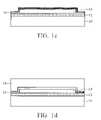
- FIGS. 1 a - 1 nare cross sections of a method for fabricating a phase-change memory element according to an embodiment of the invention.
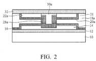
- FIG. 2is a cross section of a phase-change memory element according to another embodiment of the invention.
- a substrate 10 with a bottom electrode 12 formed thereonis provided.
- the substrate 10can be a substrate employed in a semiconductor process, such as silicon substrate.
- the substrate 10can be a substrate comprising a complementary metal oxide semiconductor (CMOS) circuit, isolation structure, diode, or capacitor.
- CMOScomplementary metal oxide semiconductor
- the accompanying drawingsshow the substrate 10 in a plain rectangle in order to simplify the illustration.
- CMOScomplementary metal oxide semiconductor
- Suitable material for the bottom electrode 12for example, is Al, W, Mo, TiN, or TiW.
- the isolation layer 14can be a silicon-containing compound, such as silicon nitride or silicon oxide.
- a dielectric layer 14is formed on the bottom electrode 12 to expose the surrounding top surface 13 of the bottom electrode 12 , wherein the bottom electrode 12 and the dielectric layer 14 formed on the bottom electrode 12 create a ladder-like configuration 15 .
- the dielectric layer 14can be a silicon-containing compound, such as silicon nitride or silicon oxide. Also, the dielectric layer 14 may constitute a bulk dielectric layer on top of an etch stop layer.
- a first electrical contact 16is conformally formed on the dielectric layer 14 to cover the ladder-like configuration 15 , wherein the first electrical contact 16 is electrically connected to the bottom electrode 12 via surrounding top surface 13 .
- Suitable material for the first electrical contact 16for example, is Al, W, Mo, TiN, or TiW.
- the thickness of the first electrical contactcan be 10 ⁇ 50 nm.
- the dielectric layer 18is formed on the first electrical contact 16 .
- the dielectric layer 18can be a silicon-containing compound, such as silicon nitride or silicon oxide.
- the dielectric layer 18is etched to remain a dielectric layer 18 a with a trench 17 .
- a second electrical contact 20is conformally formed on the dielectric layer 18 a to cover the side-walls and bottom of the trench 17 .
- the thickness of the first electrical contactcan be 10 ⁇ 50 nm. It should be noted that the depth of the trench 17 is larger than the thickness of the second electrical contact 20 .
- a dielectric layer 22is formed on and covers the second electrical contact 20 .
- the dielectric layer 22comprises silicon oxide, silicon nitride, or combinations thereof.
- the dielectric layer 22 and the second electrical conduct 20are subjected to a planarization process such as chemical mechanical polishing with the dielectric layer 18 a serving as an etching stop layer, exposing the top surface 25 of outstanding terminals 21 of the remaining second electrical contact 20 a and the top surface 23 of the remaining dielectric layer 22 a . Further, the planarization process results in coplanar top surfaces 25 and 23 , respectively, of the outstanding terminals 21 and remaining dielectric layer 22 a.
- a planarization processsuch as chemical mechanical polishing with the dielectric layer 18 a serving as an etching stop layer, exposing the top surface 25 of outstanding terminals 21 of the remaining second electrical contact 20 a and the top surface 23 of the remaining dielectric layer 22 a .
- an opening 24is formed to pass through the second electrical contact 20 a , the dielectric layer 22 a , the first electrical contact 16 and a part of the dielectric layer 14 , wherein the bottom 26 of the opening is separated from the bottom electrode 12 by the dielectric layer 14 . If the dielectric layer 14 contained an etch stop layer, that could help guarantee the separation.
- phase change layer 28is formed on the dielectric layer 22 a and filled in the opening 24 .
- the phase change layer 28can comprise In, Ge, Sb, Te or combinations thereof, such as GeTe, GeSb, SbTe, GeSbTe or InGeSbTe.
- phase change layer 28is etched back to form a phase change material block 28 a .
- the top surface 27 of the phase change material block 28 ais lower than the top surface 23 of the dielectric layer 22 a . Further, the top surface 27 of the phase change material block 28 a is also lower than the top surface 25 of the outstanding terminals 21 .
- first and second electrical contacts 16 and 20 ainterface the phase-change material block 28 a at the side-walls 29 of the phase-change material block 28 a , wherein the dimension of the cross-section areas between the phase-change material block 28 a and the first (second) electrical contacts 16 ( 20 a ) depends on the thickness of the first (second) electrical contacts 16 ( 20 a ).
- a dielectric layer 30is conformally formed on the dielectric layer 22 a and the phase-change material block 28 a .
- the dielectric layer 30comprises silicon oxide, silicon nitride, or combinations thereof. It should be noted that the total thickness of the dielectric layer 30 and the phase-change material block 28 a is larger than the depth of the opening 24 .
- the dielectric layer 30is subjected to a planarization process such as chemical mechanical polishing with the dielectric layer 22 a serving as an etching stop layer, exposing the top surface 25 of outstanding terminals 21 of the remaining second electrical contact 20 a and the top surface 31 of the remaining dielectric layer 30 a . Further, the planarization process results in coplanar top surfaces 25 and 31 , respectively, of the outstanding terminals 21 and remaining dielectric layer 30 a.
- a planarization processsuch as chemical mechanical polishing with the dielectric layer 22 a serving as an etching stop layer, exposing the top surface 25 of outstanding terminals 21 of the remaining second electrical contact 20 a and the top surface 31 of the remaining dielectric layer 30 a .
- the top electrode 32is formed on the dielectric layer 30 a and directly contacts the top surface 25 of the outstanding terminal 21 of the second electrical contact 20 a .
- Suitable material for the top electrode 32for example, is Al, W, Mo, TiN, or TiW.
- the profile of the phase-change material block 28 acan be square (referring to FIG. 1 n ), or other shapes (such as a U-shape as seen in FIG. 2 ).
- phase-change memory cellBy forming side-wall contacts to both the top and bottom electrodes of the phase-change memory cell, heating is confined at the side-walls of the block of phase-change material, which is also the location of greatest cooling. This allows for thermal uniformity to be improved compared to devices which are heated near the center of the phase-change material. Furthermore, the voltage required can be minimized by reducing the distance between the edge contacts. Also, the heating area is reduced, hence heating efficiency improved by reducing the side-wall contact thickness as well as by reducing the width of the phase-change material.
Landscapes
- Engineering & Computer Science (AREA)
- Manufacturing & Machinery (AREA)
- Semiconductor Memories (AREA)
Abstract
Description
- 1. Field of the Invention
- The invention relates to a memory element, and more particularly to a phase-change memory element and method for fabricating the same.
- 2. Description of the Related Art
- Phase-change memory technology requires high reliability, fast speeds, low current, and low operating voltage, in order to function as a viable alternative to current memory technologies such as flash and DRAM. A phase-change memory cell must therefore provide low programming current, low operating voltage, a smaller cell size, a fast phase transformation speed, and a low cost. These requirements are difficult to meet given the current state of the art.
- Current phase-change memory technology makes use of heating at the interface between a metal electrode contact and the phase-change material. More effective heating requires a smaller contact area, or equivalently a smaller heating area. A benefit of this strategy is simultaneous reduction of cell size. However, reducing the area results in higher cell resistance, which increases the required driving voltage. This is clearly not desirable. Reducing heating area does not necessarily improve other performance features. There is a large temperature gradient that exists between the contact and the bulk of the phase-change material. Phase transformation speed requires good thermal uniformity within the active region of the cell. The rate of phase-change is extremely sensitive to temperature. Non-uniform heating results in a loss of reliability due to accumulation of incomplete phase-change in the programming volume.
- United States Patent20070012905 utilizes a single edge contact to the lower electrode, while the upper electrode uses a conventional planar contact. In addition, U.S. Pat. No. 6,881,603 also minimizes only the lower electrode contact area while the upper electrode contact is planar. Meanwhile, U.S. Pat. No. 6,864,503 makes use of a phase-change material spacer with top and bottom edge contacts, however, the heating area is proportional to the electrode radius, so it is relatively large, and the upper and lower electrodes are effective heat sinks.
- Therefore, it is desirable to devise a phase-change memory cell structure that improves thermal uniformity as well as heating efficiency while allowing for a smaller heating area.
- An exemplary embodiment a phase-change memory element comprises a bottom electrode. A first dielectric layer is formed on the bottom electrode. A first electrical contact is formed on the first dielectric layer and electrically connected to the bottom electrode. A second dielectric layer is formed on and covers the first electrical contact. A second electrical contact is formed on the second dielectric layer, wherein the second electrical contact comprises an outstanding terminal. An opening passes through the second electrical contact, the second dielectric layer, and lands on the first electrical contact, wherein the bottom of the opening is separated from the bottom electrode by the first dielectric layer. A phase-change material occupies at least one portion of the opening, wherein the first and second electrical contacts interface the phase-change material at the side-walls of the phase-change material. A third dielectric layer is formed on and covers the second electrical contact and exposes a top surface of the outstanding terminal. A top electrode is formed on the third dielectric layer and directly contacts the top surface of the outstanding terminal of the second electrical contact.
- According to another embodiment of the invention, a method for fabricating a phase-change memory element is provided, comprising the following steps: providing a bottom electrode; forming a first dielectric layer on the bottom electrode, exposing the periphery of the top surface of the bottom electrode; conformally forming a first electrical contact on the first dielectric layer electrically connecting to the bottom electrode; forming a second dielectric layer with a trench to cover the first electrical contact; conformally forming a second electrical contact on the second dielectric layer; forming a third dielectric layer on the second electrical conduct; planarizing the third dielectric layer and the second electrical conduct to expose a top surface of an outstanding terminal of the second electrical conduct; forming an opening passing through the second electrical contact, the second dielectric layer, landing on the first electrical contact and separated from the bottom electrode by the first dielectric layer; filling a phase-change material into a part of the opening, forcing the first and second electrical contacts to interface the phase-change material at the side-walls of the phase-change material; filling a fourth dielectric layer into the opening, leaving coplanar top surfaces of the fourth dielectric layer and the outstanding terminal; and forming a top electrode formed on the third dielectric layer directly contacting the top surface of the outstanding terminal.
- A detailed description is given in the following embodiments with reference to the accompanying drawings.
- The invention can be more fully understood by reading the subsequent detailed description and examples with references made to the accompanying drawings, wherein:
FIGS. 1 a-1nare cross sections of a method for fabricating a phase-change memory element according to an embodiment of the invention.FIG. 2 is a cross section of a phase-change memory element according to another embodiment of the invention.- The following description is of the best-contemplated mode of carrying out the invention. This description is made for the purpose of illustrating the general principles of the invention and should not be taken in a limiting sense. The scope of the invention is best determined by reference to the appended claims.
- First, referring to
FIG. 1 a, asubstrate 10 with abottom electrode 12 formed thereon is provided. Particularly, thesubstrate 10 can be a substrate employed in a semiconductor process, such as silicon substrate. Thesubstrate 10 can be a substrate comprising a complementary metal oxide semiconductor (CMOS) circuit, isolation structure, diode, or capacitor. The accompanying drawings show thesubstrate 10 in a plain rectangle in order to simplify the illustration. Suitable material for thebottom electrode 12, for example, is Al, W, Mo, TiN, or TiW. Theisolation layer 14 can be a silicon-containing compound, such as silicon nitride or silicon oxide. - Next, referring to
FIG. 1 b, adielectric layer 14 is formed on thebottom electrode 12 to expose the surroundingtop surface 13 of thebottom electrode 12, wherein thebottom electrode 12 and thedielectric layer 14 formed on thebottom electrode 12 create a ladder-like configuration 15. Thedielectric layer 14 can be a silicon-containing compound, such as silicon nitride or silicon oxide. Also, thedielectric layer 14 may constitute a bulk dielectric layer on top of an etch stop layer. - Next, referring to
FIG. 1 c, a firstelectrical contact 16 is conformally formed on thedielectric layer 14 to cover the ladder-like configuration 15, wherein the firstelectrical contact 16 is electrically connected to thebottom electrode 12 via surroundingtop surface 13. Suitable material for the firstelectrical contact 16, for example, is Al, W, Mo, TiN, or TiW. The thickness of the first electrical contact can be 10˜50 nm. - Next, referring to
FIG. 1 d, adielectric layer 18 is formed on the firstelectrical contact 16. Thedielectric layer 18 can be a silicon-containing compound, such as silicon nitride or silicon oxide. - Next, referring to
FIG. 1 e, thedielectric layer 18 is etched to remain adielectric layer 18awith atrench 17. - Next, referring to
FIG. 1 f, a secondelectrical contact 20 is conformally formed on thedielectric layer 18ato cover the side-walls and bottom of thetrench 17. The thickness of the first electrical contact can be 10˜50 nm. It should be noted that the depth of thetrench 17 is larger than the thickness of the secondelectrical contact 20. - Next, referring to
FIG. 1 g, adielectric layer 22 is formed on and covers the secondelectrical contact 20. Thedielectric layer 22 comprises silicon oxide, silicon nitride, or combinations thereof. - Next, referring to
FIG. 1 h, thedielectric layer 22 and the secondelectrical conduct 20 are subjected to a planarization process such as chemical mechanical polishing with thedielectric layer 18aserving as an etching stop layer, exposing thetop surface 25 ofoutstanding terminals 21 of the remaining secondelectrical contact 20aand thetop surface 23 of the remainingdielectric layer 22a. Further, the planarization process results in coplanartop surfaces outstanding terminals 21 and remainingdielectric layer 22a. - Next, referring to
FIG. 1 i, anopening 24 is formed to pass through the secondelectrical contact 20a, thedielectric layer 22a, the firstelectrical contact 16 and a part of thedielectric layer 14, wherein the bottom26 of the opening is separated from thebottom electrode 12 by thedielectric layer 14. If thedielectric layer 14 contained an etch stop layer, that could help guarantee the separation. - Next, referring to
FIG. 1 j, aphase change layer 28 is formed on thedielectric layer 22aand filled in theopening 24. Thephase change layer 28 can comprise In, Ge, Sb, Te or combinations thereof, such as GeTe, GeSb, SbTe, GeSbTe or InGeSbTe. - Next, referring to
FIG. 1 k, thephase change layer 28 is etched back to form a phasechange material block 28a. It should be noted that thetop surface 27 of the phasechange material block 28ais lower than thetop surface 23 of thedielectric layer 22a. Further, thetop surface 27 of the phasechange material block 28ais also lower than thetop surface 25 of theoutstanding terminals 21. Moreover, the first and secondelectrical contacts change material block 28aat the side-walls 29 of the phase-change material block 28a, wherein the dimension of the cross-section areas between the phase-change material block 28aand the first (second) electrical contacts16 (20a) depends on the thickness of the first (second) electrical contacts16 (20a). - Next, referring to
FIG. 1 l, adielectric layer 30 is conformally formed on thedielectric layer 22aand the phase-change material block 28a. Thedielectric layer 30 comprises silicon oxide, silicon nitride, or combinations thereof. It should be noted that the total thickness of thedielectric layer 30 and the phase-change material block 28ais larger than the depth of theopening 24. - Next, referring to
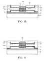
FIG. 1 m, thedielectric layer 30 is subjected to a planarization process such as chemical mechanical polishing with thedielectric layer 22aserving as an etching stop layer, exposing thetop surface 25 ofoutstanding terminals 21 of the remaining secondelectrical contact 20aand thetop surface 31 of the remainingdielectric layer 30a. Further, the planarization process results in coplanartop surfaces outstanding terminals 21 and remainingdielectric layer 30a. - Finally, referring to
FIG. 1 n, thetop electrode 32 is formed on thedielectric layer 30aand directly contacts thetop surface 25 of theoutstanding terminal 21 of the secondelectrical contact 20a. Suitable material for thetop electrode 32, for example, is Al, W, Mo, TiN, or TiW. - According to another embodiment of the invention, the profile of the phase-
change material block 28acan be square (referring toFIG. 1 n), or other shapes (such as a U-shape as seen inFIG. 2 ). - By forming side-wall contacts to both the top and bottom electrodes of the phase-change memory cell, heating is confined at the side-walls of the block of phase-change material, which is also the location of greatest cooling. This allows for thermal uniformity to be improved compared to devices which are heated near the center of the phase-change material. Furthermore, the voltage required can be minimized by reducing the distance between the edge contacts. Also, the heating area is reduced, hence heating efficiency improved by reducing the side-wall contact thickness as well as by reducing the width of the phase-change material.
- While the invention has been described by way of example and in terms of preferred embodiment, it is to be understood that the invention is not limited thereto. To the contrary, it is intended to cover various modifications and similar arrangements (as would be apparent to those skilled in the art). Therefore, the scope of the appended claims should be accorded the broadest interpretation so as to encompass all such modifications and similar arrangements.
Claims (20)
Priority Applications (7)
| Application Number | Priority Date | Filing Date | Title |
|---|---|---|---|
| US12/020,489US20090189140A1 (en) | 2008-01-25 | 2008-01-25 | Phase-change memory element |
| US12/324,871US8426838B2 (en) | 2008-01-25 | 2008-11-27 | Phase-change memory |
| TW102118217ATWI509854B (en) | 2008-01-25 | 2009-01-15 | Method for fabricating phase-change memory |
| TW098101341ATWI399876B (en) | 2008-01-25 | 2009-01-15 | Phase-change memory and method for fabricating the same |
| CN200910009855XACN101504968B (en) | 2008-01-25 | 2009-01-24 | Phase change memory device and manufacturing method thereof |
| US13/796,680US8716099B2 (en) | 2008-01-25 | 2013-03-12 | Phase-change memory |
| US14/191,016US9087985B2 (en) | 2008-01-25 | 2014-02-26 | Phase-change memory |
Applications Claiming Priority (1)
| Application Number | Priority Date | Filing Date | Title |
|---|---|---|---|
| US12/020,489US20090189140A1 (en) | 2008-01-25 | 2008-01-25 | Phase-change memory element |
Related Child Applications (1)
| Application Number | Title | Priority Date | Filing Date |
|---|---|---|---|
| US12/324,871Continuation-In-PartUS8426838B2 (en) | 2008-01-25 | 2008-11-27 | Phase-change memory |
Publications (1)
| Publication Number | Publication Date |
|---|---|
| US20090189140A1true US20090189140A1 (en) | 2009-07-30 |
Family
ID=40898297
Family Applications (1)
| Application Number | Title | Priority Date | Filing Date |
|---|---|---|---|
| US12/020,489AbandonedUS20090189140A1 (en) | 2008-01-25 | 2008-01-25 | Phase-change memory element |
Country Status (2)
| Country | Link |
|---|---|
| US (1) | US20090189140A1 (en) |
| CN (1) | CN101504968B (en) |
Cited By (2)
| Publication number | Priority date | Publication date | Assignee | Title |
|---|---|---|---|---|
| US20100117050A1 (en)* | 2008-11-12 | 2010-05-13 | Industrial Technology Research Institute | Phase-change memory element |
| US8426838B2 (en) | 2008-01-25 | 2013-04-23 | Higgs Opl. Capital Llc | Phase-change memory |
Families Citing this family (7)
| Publication number | Priority date | Publication date | Assignee | Title |
|---|---|---|---|---|
| TWI347607B (en) | 2007-11-08 | 2011-08-21 | Ind Tech Res Inst | Writing system and method for a phase change memory |
| TWI402845B (en) | 2008-12-30 | 2013-07-21 | Higgs Opl Capital Llc | Verification circuits and methods for phase change memory |
| TWI412124B (en) | 2008-12-31 | 2013-10-11 | Higgs Opl Capital Llc | Phase change memory |
| CN103427022B (en)* | 2013-08-22 | 2016-07-06 | 中国科学院上海微系统与信息技术研究所 | The preparation method comprising the phase change storage structure of sandwich type electrode |
| CN105702858B (en)* | 2016-03-23 | 2018-05-25 | 江苏时代全芯存储科技有限公司 | Phase change memory and its manufacturing method |
| CN108630806A (en)* | 2017-03-17 | 2018-10-09 | 中芯国际集成电路制造(上海)有限公司 | Phase transition storage and forming method thereof |
| CN109888091B (en)* | 2019-03-01 | 2023-12-01 | 上海华力微电子有限公司 | Method for forming random access memory layer |
Citations (3)
| Publication number | Priority date | Publication date | Assignee | Title |
|---|---|---|---|---|
| US6864503B2 (en)* | 2002-08-09 | 2005-03-08 | Macronix International Co., Ltd. | Spacer chalcogenide memory method and device |
| US6881603B2 (en)* | 2001-12-31 | 2005-04-19 | Intel Corporation | Phase change material memory device |
| US20070012905A1 (en)* | 2005-07-13 | 2007-01-18 | Taiwan Semiconductor Manufacturing Company, Ltd. | Novel phase change random access memory |
- 2008
- 2008-01-25USUS12/020,489patent/US20090189140A1/ennot_activeAbandoned
- 2009
- 2009-01-24CNCN200910009855XApatent/CN101504968B/enactiveActive
Patent Citations (3)
| Publication number | Priority date | Publication date | Assignee | Title |
|---|---|---|---|---|
| US6881603B2 (en)* | 2001-12-31 | 2005-04-19 | Intel Corporation | Phase change material memory device |
| US6864503B2 (en)* | 2002-08-09 | 2005-03-08 | Macronix International Co., Ltd. | Spacer chalcogenide memory method and device |
| US20070012905A1 (en)* | 2005-07-13 | 2007-01-18 | Taiwan Semiconductor Manufacturing Company, Ltd. | Novel phase change random access memory |
Cited By (9)
| Publication number | Priority date | Publication date | Assignee | Title |
|---|---|---|---|---|
| US8426838B2 (en) | 2008-01-25 | 2013-04-23 | Higgs Opl. Capital Llc | Phase-change memory |
| US8716099B2 (en) | 2008-01-25 | 2014-05-06 | Higgs Opl. Capital Llc | Phase-change memory |
| US9087985B2 (en) | 2008-01-25 | 2015-07-21 | Higgs Opl.Capital Llc | Phase-change memory |
| US20100117050A1 (en)* | 2008-11-12 | 2010-05-13 | Industrial Technology Research Institute | Phase-change memory element |
| US8604457B2 (en) | 2008-11-12 | 2013-12-10 | Higgs Opl. Capital Llc | Phase-change memory element |
| US8884260B2 (en) | 2008-11-12 | 2014-11-11 | Higgs Opl. Capital Llc | Phase change memory element |
| US9245924B2 (en) | 2008-11-12 | 2016-01-26 | Higgs Opl. Capital Llc | Phase change memory element |
| US9735352B2 (en) | 2008-11-12 | 2017-08-15 | Gula Consulting Limited Liability Company | Phase change memory element |
| US10573807B2 (en) | 2008-11-12 | 2020-02-25 | Gula Consulting Limited Liability Company | Phase change memory element |
Also Published As
| Publication number | Publication date |
|---|---|
| CN101504968B (en) | 2011-12-28 |
| CN101504968A (en) | 2009-08-12 |
Similar Documents
| Publication | Publication Date | Title |
|---|---|---|
| US9087985B2 (en) | Phase-change memory | |
| US20090189140A1 (en) | Phase-change memory element | |
| US7888155B2 (en) | Phase-change memory element and method for fabricating the same | |
| US10573807B2 (en) | Phase change memory element | |
| US7679163B2 (en) | Phase-change memory element | |
| US7964862B2 (en) | Phase change memory devices and methods for manufacturing the same | |
| US7855378B2 (en) | Phase change memory devices and methods for fabricating the same | |
| US7923286B2 (en) | Method of fabricating a phase-change memory | |
| US7919768B2 (en) | Phase-change memory element | |
| US20090008621A1 (en) | Phase-change memory element | |
| US20090057640A1 (en) | Phase-change memory element | |
| KR20040033017A (en) | Phase Change Material Memory Device | |
| US20080283812A1 (en) | Phase-change memory element | |
| US7675054B2 (en) | Phase change memory devices and methods for fabricating the same | |
| US20080186762A1 (en) | Phase-change memory element | |
| CN104851976A (en) | Phase-change memory and manufacturing method thereof | |
| CN101399314B (en) | Phase change memory and manufacturing method thereof | |
| CN1988200A (en) | Spacer electrode side-connected phase change memory and manufacturing method thereof | |
| CN114762142B (en) | Phase change memory and method for manufacturing the same | |
| US20090101880A1 (en) | Phase change memory devices and methods for fabricating the same |
Legal Events
| Date | Code | Title | Description |
|---|---|---|---|
| AS | Assignment | Owner name:NANYA TECHNOLOGY CORPORATION, TAIWAN Free format text:ASSIGNMENT OF ASSIGNORS INTEREST;ASSIGNOR:CHEN, FREDERICK T.;REEL/FRAME:020428/0636 Effective date:20071109 Owner name:POWERCHIP SEMICONDUCTOR CORP., TAIWAN Free format text:ASSIGNMENT OF ASSIGNORS INTEREST;ASSIGNOR:CHEN, FREDERICK T.;REEL/FRAME:020428/0636 Effective date:20071109 Owner name:POROMOS TECHNOLOGIES, INC., TAIWAN Free format text:ASSIGNMENT OF ASSIGNORS INTEREST;ASSIGNOR:CHEN, FREDERICK T.;REEL/FRAME:020428/0636 Effective date:20071109 Owner name:INDUSTRIAL TECHNOLOGY RESEARCH INSTITUTE, TAIWAN Free format text:ASSIGNMENT OF ASSIGNORS INTEREST;ASSIGNOR:CHEN, FREDERICK T.;REEL/FRAME:020428/0636 Effective date:20071109 Owner name:WINBOND ELECTRONICS CORP., TAIWAN Free format text:ASSIGNMENT OF ASSIGNORS INTEREST;ASSIGNOR:CHEN, FREDERICK T.;REEL/FRAME:020428/0636 Effective date:20071109 | |
| AS | Assignment | Owner name:INDUSTRIAL TECHNOLOGY RESEARCH INSTITUTE,TAIWAN Free format text:ASSIGNMENT OF ASSIGNORS INTEREST;ASSIGNORS:POWERCHIP SEMICONDUCTOR CORP.;NANYA TECHNOLOGY CORPORATION;PROMOS TECHNOLOGIES INC.;AND OTHERS;SIGNING DATES FROM 20091209 TO 20100125;REEL/FRAME:024149/0102 Owner name:INDUSTRIAL TECHNOLOGY RESEARCH INSTITUTE, TAIWAN Free format text:ASSIGNMENT OF ASSIGNORS INTEREST;ASSIGNORS:POWERCHIP SEMICONDUCTOR CORP.;NANYA TECHNOLOGY CORPORATION;PROMOS TECHNOLOGIES INC.;AND OTHERS;SIGNING DATES FROM 20091209 TO 20100125;REEL/FRAME:024149/0102 | |
| STCB | Information on status: application discontinuation | Free format text:ABANDONED -- FAILURE TO RESPOND TO AN OFFICE ACTION |