US20090186485A1 - Sub-lithographic printing method - Google Patents
Sub-lithographic printing methodDownload PDFInfo
- Publication number
- US20090186485A1 US20090186485A1US12/018,316US1831608AUS2009186485A1US 20090186485 A1US20090186485 A1US 20090186485A1US 1831608 AUS1831608 AUS 1831608AUS 2009186485 A1US2009186485 A1US 2009186485A1
- Authority
- US
- United States
- Prior art keywords
- spacer
- trenches
- substrate
- forming
- spacers
- Prior art date
- Legal status (The legal status is an assumption and is not a legal conclusion. Google has not performed a legal analysis and makes no representation as to the accuracy of the status listed.)
- Granted
Links
- 238000000034methodMethods0.000titleclaimsabstractdescription41
- 125000006850spacer groupChemical group0.000claimsabstractdescription248
- 239000000463materialSubstances0.000claimsabstractdescription155
- 239000000758substrateSubstances0.000claimsabstractdescription53
- 229910021420polycrystalline siliconInorganic materials0.000claimsdescription18
- XUIMIQQOPSSXEZ-UHFFFAOYSA-NSiliconChemical compound[Si]XUIMIQQOPSSXEZ-UHFFFAOYSA-N0.000claimsdescription15
- 229910052710siliconInorganic materials0.000claimsdescription15
- 239000010703siliconSubstances0.000claimsdescription15
- VYPSYNLAJGMNEJ-UHFFFAOYSA-NSilicium dioxideChemical compoundO=[Si]=OVYPSYNLAJGMNEJ-UHFFFAOYSA-N0.000claimsdescription8
- 238000000151depositionMethods0.000claimsdescription7
- 239000000377silicon dioxideSubstances0.000claimsdescription4
- 235000012239silicon dioxideNutrition0.000claimsdescription4
- 229910052581Si3N4Inorganic materials0.000claimsdescription3
- HQVNEWCFYHHQES-UHFFFAOYSA-Nsilicon nitrideChemical compoundN12[Si]34N5[Si]62N3[Si]51N64HQVNEWCFYHHQES-UHFFFAOYSA-N0.000claimsdescription3
- 238000005498polishingMethods0.000claims2
- 230000001419dependent effectEffects0.000abstractdescription6
- 230000015572biosynthetic processEffects0.000description19
- KWYUFKZDYYNOTN-UHFFFAOYSA-MPotassium hydroxideChemical compound[OH-].[K+]KWYUFKZDYYNOTN-UHFFFAOYSA-M0.000description15
- 238000005530etchingMethods0.000description13
- 230000015654memoryEffects0.000description10
- 238000005229chemical vapour depositionMethods0.000description6
- 235000012431wafersNutrition0.000description6
- 239000007789gasSubstances0.000description4
- 239000011810insulating materialSubstances0.000description4
- 239000004065semiconductorSubstances0.000description4
- 238000003491arrayMethods0.000description3
- 230000008021depositionEffects0.000description3
- NBIIXXVUZAFLBC-UHFFFAOYSA-NPhosphoric acidChemical compoundOP(O)(O)=ONBIIXXVUZAFLBC-UHFFFAOYSA-N0.000description2
- KFZMGEQAYNKOFK-UHFFFAOYSA-Nisopropyl alcoholNatural productsCC(C)OKFZMGEQAYNKOFK-UHFFFAOYSA-N0.000description2
- 229910000147aluminium phosphateInorganic materials0.000description1
- 239000004020conductorSubstances0.000description1
- 230000003247decreasing effectEffects0.000description1
- 125000001449isopropyl groupChemical group[H]C([H])([H])C([H])(*)C([H])([H])[H]0.000description1
- 238000012986modificationMethods0.000description1
- 230000004048modificationEffects0.000description1
- 238000000206photolithographyMethods0.000description1
- 239000000126substanceSubstances0.000description1
Images


Classifications
- H—ELECTRICITY
- H01—ELECTRIC ELEMENTS
- H01L—SEMICONDUCTOR DEVICES NOT COVERED BY CLASS H10
- H01L21/00—Processes or apparatus adapted for the manufacture or treatment of semiconductor or solid state devices or of parts thereof
- H01L21/02—Manufacture or treatment of semiconductor devices or of parts thereof
- H01L21/027—Making masks on semiconductor bodies for further photolithographic processing not provided for in group H01L21/18 or H01L21/34
- H01L21/033—Making masks on semiconductor bodies for further photolithographic processing not provided for in group H01L21/18 or H01L21/34 comprising inorganic layers
- H01L21/0334—Making masks on semiconductor bodies for further photolithographic processing not provided for in group H01L21/18 or H01L21/34 comprising inorganic layers characterised by their size, orientation, disposition, behaviour, shape, in horizontal or vertical plane
- H01L21/0337—Making masks on semiconductor bodies for further photolithographic processing not provided for in group H01L21/18 or H01L21/34 comprising inorganic layers characterised by their size, orientation, disposition, behaviour, shape, in horizontal or vertical plane characterised by the process involved to create the mask, e.g. lift-off masks, sidewalls, or to modify the mask, e.g. pre-treatment, post-treatment
- H—ELECTRICITY
- H01—ELECTRIC ELEMENTS
- H01L—SEMICONDUCTOR DEVICES NOT COVERED BY CLASS H10
- H01L21/00—Processes or apparatus adapted for the manufacture or treatment of semiconductor or solid state devices or of parts thereof
- H01L21/70—Manufacture or treatment of devices consisting of a plurality of solid state components formed in or on a common substrate or of parts thereof; Manufacture of integrated circuit devices or of parts thereof
- H01L21/71—Manufacture of specific parts of devices defined in group H01L21/70
- H01L21/768—Applying interconnections to be used for carrying current between separate components within a device comprising conductors and dielectrics
- H01L21/76801—Applying interconnections to be used for carrying current between separate components within a device comprising conductors and dielectrics characterised by the formation and the after-treatment of the dielectrics, e.g. smoothing
- H01L21/76802—Applying interconnections to be used for carrying current between separate components within a device comprising conductors and dielectrics characterised by the formation and the after-treatment of the dielectrics, e.g. smoothing by forming openings in dielectrics
- H01L21/76816—Aspects relating to the layout of the pattern or to the size of vias or trenches
Definitions
- the present inventionrelates to formation of trench structures over a substrate, and more particularly to a method of forming sub-lithographic trench structures.
- Typical semiconductor computer memoriesare fabricated on semiconductor substrates consisting of arrays of large number of physical memory cells.
- the memory cells in these memory arraysare generally connected by conductive channels carrying electrical current between individual memory cells, the memory array, and a memory controller.
- These conductive channelsare often referred to as “bit-lines” and “word-lines”.
- bit-linesand word-lines.
- word-linesAs memory cells and memory arrays have decreased in size, the conductive channels connecting forming the connections between the cells and array must also decrease in size.
- Conductive channels formed on the substratemay be formed with a variety of methods.
- One common methodis to deposit conductive material directly into a trench structure on the substrate.
- methods used for trench structure formationinclude at least one step involving photolithography.
- the photolithographic methods employed for the formation of conductive channels and other structures formed on a substrateare typically limited by the wavelength of deep ultraviolet (DUV) a photolithographic tool uses.
- DUVdeep ultraviolet
- An exemplary embodiment of the present inventionis a method for forming trench structures disposed over a substrate.
- the substratecan be, but is not limited to, bare silicon substrate or silicon substrate with a layer of insulating material deposited on the top surface of the silicon substrate.
- the method for forming trench structures disposed over a substrateentails depositing a sacrificial layer of a sacrificial material over the substrate.
- a forming stepforms a first set of trenches in the sacrificial layer with a lithographic mask, etching of the exposed sacrificial layer, and removal of the lithographic mask.
- a filling stepcompletely fills the first set of trenches with a first set of step spacer blocks.
- the first set of step spacer blocksincludes two alternating spacer materials with each spacer material separately removable from the other and the sacrificial material.
- a second forming stepforms a second set of trenches by selectively removing the remaining sacrificial material.
- a second filling stepcompletely fills the second set of trenches with a second set of step spacer blocks comprising the same two alternating spacer materials.
- the alternating spacer materialscontinue in sequence with the alternating spacer materials in the first set of step spacer blocks.
- Another forming stepforms a hard mask by selectively removing one of the two alternating spacer materials.
- an etching stepetches a trench structure into the substrate or insulating material with the hard mask.
- Another exemplary aspect of the present inventionis an integrated circuit comprising a trench structure disposed over a substrate.
- the integrated circuitis formed at least in part by the deposition of a sacrificial layer of a sacrificial material over the substrate.
- a first set of trenchesis formed in the sacrificial layer.
- the first set of trenchesis completely filled with a first set of step spacer blocks using two alternating spacer materials that are separately removable
- a second set of trenchesis formed by selectively removing the remaining sacrificial material after filling the first set of trenches.
- the second set of trenchesare completely filled with a second set of step spacer blocks using the same two alternating spacer materials as the first set of spacer blocks, with the two alternating spacer materials continuing in sequence with the alternating spacer materials in the first set of step spacer blocks.
- One of the two alternating spacer materialsis selectively removed, thereby forming a hard mask above the substrate.
- the hard maskis utilized to etch the trench structure in the substrate of the integrated circuit.
- a further exemplary aspect of the present inventionis a trench structure disposed over a substrate.
- the trench structureis formed at least in part by the deposition of a sacrificial layer of a sacrificial material over the substrate.
- a first set of trenchesis formed in the sacrificial layer.
- the first set of trenchesis completely filled with a first set of step spacer blocks using two alternating spacer materials that are separately removable
- a second set of trenchesis formed by selectively removing the remaining sacrificial material after filling the first set of trenches.
- the second set of trenchesare completely filled with a second set of step spacer blocks using the same two alternating spacer materials as the first set of spacer blocks, with the two alternating spacer materials continuing in sequence with the alternating spacer materials in the first set of step spacer blocks.
- One of the two alternating spacer materialsis selectively removed, thereby forming a hard mask above the substrate.
- the hard maskis utilized to etch the trench structure in the substrate.
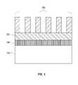
- FIG. 1illustrates a starting wafer
- FIG. 2illustrates a deposition of sacrificial material.
- FIG. 3illustrates the formation of a lithographic mask.
- FIG. 4illustrates the formation of a first set of trenches.
- FIGS. 5-10illustrate the formation of a first set of step spacer blocks.
- FIG. 11illustrates the formation of a second set of trenches.
- FIGS. 12-17illustrate the formation of a second set of step spacer blocks.
- FIG. 18illustrates the formation of a hard mask.
- FIG. 19illustrates the formation of trench structures in the substrate.
- FIG. 20illustrates the removal of the hard mask.
- the present inventionwill be described with reference to FIGS. 1-20 .
- like elements shown throughoutare indicated with like reference numerals.
- the embodiments of the present inventionare generally directed to, but are not limited to, forming sub-lithographic trenches in semiconductor substrates. These sub-lithographic trenches may be used, for example, in the formation of bit-lines and word-lines in a memory array or integrated circuit in semi-conductor computer memory.
- FIG. 1illustrates an exemplary embodiment of a starting wafer 102 .
- the exemplary embodiment of the starting wafer 102is comprised of a silicon substrate 104 and an insulating layer 106 .
- the insulating layer 106may be comprised of only one material or the insulating layer 106 may itself be comprised of several layers of insulating materials. Those skilled in the art will recognize that a variety of insulating materials may be used. In one embodiment of the invention the insulating layer 106 is comprised of silicon dioxide.
- the starting wafer 102is only comprised of the silicon substrate 104 . Additionally, those skilled in the art will recognize that a variety of front end of line (FEOL) wafers may be used as the starting wafer 102 .
- FEOLfront end of line
- a sacrificial layer 202is deposited on top of the insulating layer 106 .
- the sacrificial layer 202is comprised of silicon nitride. The only limiting factor to the material used for the sacrificial layer 202 is that it must be separately removable from the insulating layer 106 and/or the silicon substrate 104 .
- CVDchemical vapor deposition
- FIG. 3shows a formation of a lithographic mask 302 deposited above the sacrificial layer 202 .
- the lithographic mask 302may be of any pattern as long as it is able to form trenches in the sacrificial layer 202 upon the etching of the sacrificial layer 202 .
- the employment of lithographic masks to form lithographic featuresis well known in the art and is disclosed, for example, in U.S. Pat. No. 6,358,813 issued to Holmes et al. U.S. Pat. No. 6,358,813 is incorporated herein by reference.
- FIG. 4illustrates a formation of a first set of trenches 402 and the removal of the lithographic mask.
- the first set of trenches 402are created by etching the sacrificial layer not covered by the lithographic mask.
- the etching of the sacrificial layershould selectively remove the exposed areas of the sacrificial layer and stop on the silicon substrate 104 or the insulating layer 106 .
- dry etchesmay be utilized in this process.
- An example of a dry etchwould be reactive ion etch (RIE).
- RIEreactive ion etch
- RIEreactive ion etch
- FIG. 4also illustrates a lithographic mask's feature size 404 .
- the lithographic mask's feature sizeis typically limited to the wavelength of deep ultraviolet (DUV) light a photolithographic tool uses.
- the lithographic mask's feature sizewill be relevant later in the process when step spacers and spacer plugs are deposed into the first set of trenches 402 .
- DUVdeep ultraviolet
- a layer of first spacer material 502is deposited over the structures formed by the etching of the sacrificial layer, over the bottom of the first set of trenches, and sidewalls of the first set of trenches.
- a variety of spacer materialscan be used for the layer of first spacer material 502 .
- the layer of first spacer material 502is comprised of intrinsic polycrystalline silicon.
- the layer of first spacer material 502may be comprised of P-doped polycrystalline silicon or N-doped polycrystalline silicon.
- first spacer material 502The only limiting factor to selection of the first spacer material is that it must be separately removable from the sacrificial layer, the insulating layer 106 (if there is an insulating layer 106 ), and the silicon substrate 104 . Again, those skilled in the art will recognize that a variety of CVD processes may be employed to deposit the layer of first spacer material 502 .
- the thickness of the layer of first spacer material 502is one-eighth of the lithographic mask's feature size.
- the thickness of the layer of first spacer material 502is one-half of one-nth of the lithographic mask's feature size.
- nis an even integer equal or greater than 2.
- FIG. 6illustrates a formation of first pairs of step spacers 602 in the first set of trenches 402 .
- the first pairs of step spacers 602are formed along the sidewalls of the first set of trenches 402 .
- the first pairs of step spacers 602are created by etching the layer of first spacer material with a directional dry etch removing the first spacer material over the sacrificial layer and removing the first spacer material over the bottom of the first set of trenches 402 .
- a directional dry etchesmay be used to form the first pairs of step spacers 602 .
- An example of such a directional dry etchis a spacer RIE. The gases used for the RIE will be dependent on the type of first spacer material used.
- a layer of second spacer material 702is deposited over the structures formed by the etching of the sacrificial layer, along the sidewalls of the first pairs of step spacers, and over the bottom of the first set of trenches.
- spacer materialsmay be used for the layer of second spacer material 702 .
- the layer of second spacer material 702is comprised of P-doped polycrystalline silicon.
- the layer of second spacer material 702may be comprised of intrinsic polycrystalline silicon or N-doped polycrystalline silicon.
- the second spacer material 502The only limiting factor to selection of the second spacer material is that it must be separately removable from the sacrificial layer, the insulating layer 106 , if there is an insulating layer 106 , the silicon substrate 104 , and the first spacer material. Again, those skilled in the art will recognize that a variety of CVD processes may be employed to deposit the layer of second spacer material 502 .
- the thickness of the layer of second spacer material 702is one-quarter of the lithographic mask's feature size. In an alternate embodiment where the final trench structure's size is one-nth of the lithographic mask's feature size, the thickness of the layer of second spacer material 702 is one-nth of the lithographic mask's feature size. In this alternate embodiment of the invention, n is an even integer equal or greater than 2. Again, one skilled in the art will recognize that the thickness of the layer of second spacer material 502 can be of an arbitrary thickness depending on the pattern desired.
- FIG. 8shows a formation of second pairs of step spacers 802 in the first set of trenches 402 .
- the second pairs of step spacers 802are formed along the sidewalls of the first pairs of step spacers.
- the second pairs of step spacers 802are created by etching the layer of second spacer material with a directional dry etch removing the second spacer material over the sacrificial layer and removing the second spacer material over the bottom of the first set of trenches 402 .
- a directional dry etchesmay be used to form the second pairs of step spacers 802 .
- An example of such a directional dry etchis a spacer RIE. The gases used for the RIE will be dependent on the type of second spacer material used.
- the processes shown in FIGS. 5-8are performed n/2 times.
- the kth pair of step spacersare formed along the inside walls of the (k ⁇ 1)th pair of step spacers if k is greater than 1 and equal or less than n/2.
- the kth pair of step spacersis formed along the inside walls of the first set of trenches and the inside walls of the second set of trenches if k is equal to 1.
- the kth pair of step spacersis formed using the first spacer material if k is odd, the kth pair of step spacers is formed using the second spacer material if k is even, n being a positive even integer equal or greater than 2.
- a plug layer of first spacer material 902is deposited above the remaining structures of the sacrificial layer and completely filling the first set of trenches between the sidewalls of the second pairs of step spacers.
- the plug layer of first spacer material 902forms spacer plugs 904 in the first set of trenches.
- the plug layer of first spacer material 902is comprised of the first spacer material.
- the thickness of the plug layer of first spacer material 902is at least one-quarter of the lithographic mask's feature size. In an alternate embodiment where the final trench structure's size is one-nth of the lithographic mask's feature size, the thickness of the plug layer of first spacer material 902 is at least one-nth of the lithographic mask's feature size. Again, in this alternate embodiment of the invention, n is an even integer equal or greater than 2.
- the thickness of the plug layer of first spacer material 902can be of an arbitrary thickness depending on the pattern desired.
- FIG. 10illustrates a chemical mechanical polish (CMP) of the remaining sacrificial material 202 , the first pairs of step spacers 602 , the second pairs of step spacers 802 , and the spacer plugs 904 .
- the first pairs of step spacers 602 , the second pairs of step spacer 802 , and the spacer plugs 904 in the first set of trenchesform a first set of step spacer blocks 1002 filling the first set of trenches.
- the CMPshould polish the remaining sacrificial layer 202 and first set of step spacer blocks 1002 such that the surface of the remaining sacrificial layer 202 and the surface of the first set of step spacer blocks 1002 are substantially parallel to the top surface of the silicon substrate 104 .
- FIG. 11shows a formation of a second set of trenches 1102 .
- the second set of trenches 1102are formed by removing the remaining sacrificial material such that the sidewalls of the first set of step spacer blocks 1002 serve as the sidewalls of the second set of trenches 1102 .
- the sacrificial materialis silicon nitride
- the remaining sacrificial materialis removed by a hot phosphoric acid wet etch.
- a variety of materialscan be used for the sacrificial material. Therefore the specific etch used must be able to separately remove the sacrificial material from the first spacer material, the second spacer material, the insulating layer 106 , and/or the silicon substrate 104 .
- a second layer of first spacer material 1202is deposited along the top surface of the first set of step spacer blocks, along the sidewalls of the first set of step spacer blocks, and along the bottom of the second set of trenches.
- the second layer of first spacer material 1202is comprised of the same material used for the layer of first spacer material. As stated above, a variety of materials can be used and a variety of CVD processes may be employed to deposit the material onto the structures.
- the thickness of the second layer of first spacer material 1202is one-eighth of the lithographic mask's feature size. In an alternate embodiment of the invention where the final trench structure's size is one-nth of the lithographic mask's feature size, the thickness of the second layer of first spacer material 1202 is one-half of one-nth of the lithographic mask's feature size. In this alternate embodiment of the invention, n is an even integer equal or greater than 2.
- the thickness of the second layer of first spacer material 1202can be of an arbitrary thickness depending on the pattern desired.
- FIG. 13shows a formation of first pairs of step spacers 1302 in the second set of trenches 1102 .
- the first pairs of step spacers 1302are formed along the sidewalls of the second set of trenches 1102 .
- the first pairs of step spacers 1302are created by etching the layer of first spacer material with a directional dry etch removing the first spacer material over the sacrificial layer and removing the first spacer material over the bottom of the second set of trenches 1102 .
- a spacer RIEis employed. The gases used for the RIE being dependent on the type of first spacer material used.
- a second layer of second spacer material 1402is deposited over the first set of step spacer blocks, along the sidewalls of the first pairs of step spacers in the second set of trenches, and over the bottom of the second set of trenches.
- the second layer of second spacer material 1402is comprised of the same material used for the layer of second spacer material. As stated above, a variety of materials can be used and a variety of CVD processes may be employed to deposit the material onto the structures.
- the thickness of the second layer of second spacer material 1402is one-quarter of the lithographic mask's feature size. In an alternate embodiment where the final trench structure's size is one-nth of the lithographic mask's feature size, the thickness of the second layer of second spacer material 1402 is one-nth of the lithographic mask's feature size. Again, in this alternate embodiment of the invention, n is an even integer equal or greater than 2.
- the thickness of the second layer of first spacer material 1402can be of an arbitrary thickness depending on the pattern desired.
- FIG. 15shows a formation of second pairs of step spacers 1502 in the second set of trenches 1102 .
- the second pairs of step spacers 1502are formed along the sidewalls of the first pairs of step spacers.
- the second pairs of step spacers 1502are created by etching the second layer of second spacer material with a directional dry etch removing the second spacer material over the first set of step spacer blocks and removing the second spacer material over the bottom of the second set of trenches 1102 .
- a spacer RIEis employed. The gases used for the RIE being dependent on the type of second spacer material used.
- the processes shown in FIGS. 12-15are performed n/2 times.
- the kth pair of step spacersare formed along the inside walls of the (k ⁇ 1)th pair of step spacers if k is greater than 1 and equal or less than n/2.
- the kth pair of step spacersis formed along the inside walls of the first set of trenches and the inside walls of the second set of trenches if k is equal to 1.
- the kth pair of step spacersis formed using the first spacer material if k is odd, the kth pair of step spacers is formed using the second spacer material if k is even, n being a positive even integer equal or greater than 2.
- a plug layer of first spacer material 1602is deposited above the first set of step spacer blocks and completely filling the second set of trenches between the sidewalls of the second pairs of step spacers.
- the plug layer of first spacer material 1602forms spacer plugs 1604 in the second set of trenches.
- the plug layer of first spacer material 1602is the first spacer material.
- the thickness of the plug layer of first spacer material 1602is at least one-quarter of the lithographic mask's feature size. In an alternate embodiment where the final trench structure's size is one-nth of the lithographic mask's feature size, the thickness of the plug layer of first spacer material 1602 is at least one-nth of the lithographic mask's feature size. Again, in this alternate embodiment of the invention, n is an even integer equal or greater than 2.
- the thickness of the plug layer of first spacer material 1602can be of an arbitrary thickness depending on the pattern desired.
- FIG. 17illustrates a second CMP of the first set of step spacer blocks 1004 , the first pairs of step spacers 1302 , the second pairs of step spacers 1502 , and the spacer plugs 1604 .
- the first pairs of step spacers 1302 , the second pairs of step spacer 1502 , and the spacer plugs 1604 in the second set of trenchesform a second set of step spacer blocks 1702 filling the second set of trenches.
- the CMPshould polish the first set of step spacer blocks 1002 and second set of step spacer blocks 1702 such that the surface of the first set of step spacer blocks 1002 and the surface of the second set of step spacer blocks 1702 are parallel to the top surface of the silicon substrate 104 .
- a hard mask 1802is formed.
- the hard mask 1802is created by selectively removing one of the two spacer materials. If the spacer material to be stripped is intrinsic polycrystalline silicon, a potassium hydroxide/isopropyl alcohol (KOH/IPA) solution is used to remove the spacer material. If the spacer material to be removed is P-doped polycrystalline silicon, a KOH solution is used to remove the spacer material. Again, if alternate spacer materials are utilized alternate wet etches or dry etches must be employed to remove the spacer materials.
- KOH/IPApotassium hydroxide/isopropyl alcohol
- FIG. 19shows a formation of the final trench structure 1902 . This is accomplished by etching into the substrate with the hard mask 1802 .
- the insulating layer 106is silicon dioxide
- a sub-lithographic silicon dioxide RIEis utilized.
- a sub-lithographic silicon RIEis utilized. The sub-lithographic RIE used in etching into the substrate is dependent upon the substrate 104 and the insulating layer 106 deposited above the substrate 104 if an insulating layer 106 is employed.
- the hard maskis selectively removed from the insulating layer 106 , if an insulating layer 106 is used, and/or the silicon substrate 104 .
- a KOH solutionis used to remove the hard mask.
- a KOH/IPA solutionis used to remove the hard mask. The wet or dry etch used to remove the hard mask depends on the composition of the hard mask and the selectivity of the etchant towards the substrate 104 and insulating layer 106 .
Landscapes
- Engineering & Computer Science (AREA)
- Physics & Mathematics (AREA)
- Condensed Matter Physics & Semiconductors (AREA)
- General Physics & Mathematics (AREA)
- Manufacturing & Machinery (AREA)
- Computer Hardware Design (AREA)
- Microelectronics & Electronic Packaging (AREA)
- Power Engineering (AREA)
- Chemical & Material Sciences (AREA)
- Inorganic Chemistry (AREA)
- Semiconductor Memories (AREA)
Abstract
Description
- 1. Field of the Invention
- The present invention relates to formation of trench structures over a substrate, and more particularly to a method of forming sub-lithographic trench structures.
- 2.Description of Background
- Typical semiconductor computer memories are fabricated on semiconductor substrates consisting of arrays of large number of physical memory cells. The memory cells in these memory arrays are generally connected by conductive channels carrying electrical current between individual memory cells, the memory array, and a memory controller. These conductive channels are often referred to as “bit-lines” and “word-lines”. As memory cells and memory arrays have decreased in size, the conductive channels connecting forming the connections between the cells and array must also decrease in size.
- Conductive channels formed on the substrate may be formed with a variety of methods. One common method is to deposit conductive material directly into a trench structure on the substrate. Often, methods used for trench structure formation include at least one step involving photolithography. The photolithographic methods employed for the formation of conductive channels and other structures formed on a substrate are typically limited by the wavelength of deep ultraviolet (DUV) a photolithographic tool uses. Thus, it is desirable to devise a method to form trench structures not limited by the specifications of the photolithographic tool being used.
- An exemplary embodiment of the present invention is a method for forming trench structures disposed over a substrate. The substrate can be, but is not limited to, bare silicon substrate or silicon substrate with a layer of insulating material deposited on the top surface of the silicon substrate.
- The method for forming trench structures disposed over a substrate entails depositing a sacrificial layer of a sacrificial material over the substrate. A forming step forms a first set of trenches in the sacrificial layer with a lithographic mask, etching of the exposed sacrificial layer, and removal of the lithographic mask. A filling step completely fills the first set of trenches with a first set of step spacer blocks. The first set of step spacer blocks includes two alternating spacer materials with each spacer material separately removable from the other and the sacrificial material. A second forming step forms a second set of trenches by selectively removing the remaining sacrificial material. A second filling step completely fills the second set of trenches with a second set of step spacer blocks comprising the same two alternating spacer materials. The alternating spacer materials continue in sequence with the alternating spacer materials in the first set of step spacer blocks. Another forming step forms a hard mask by selectively removing one of the two alternating spacer materials. Finally, an etching step etches a trench structure into the substrate or insulating material with the hard mask.
- Another exemplary aspect of the present invention is an integrated circuit comprising a trench structure disposed over a substrate. The integrated circuit is formed at least in part by the deposition of a sacrificial layer of a sacrificial material over the substrate. A first set of trenches is formed in the sacrificial layer. The first set of trenches is completely filled with a first set of step spacer blocks using two alternating spacer materials that are separately removable A second set of trenches is formed by selectively removing the remaining sacrificial material after filling the first set of trenches. The second set of trenches are completely filled with a second set of step spacer blocks using the same two alternating spacer materials as the first set of spacer blocks, with the two alternating spacer materials continuing in sequence with the alternating spacer materials in the first set of step spacer blocks. One of the two alternating spacer materials is selectively removed, thereby forming a hard mask above the substrate. Finally, the hard mask is utilized to etch the trench structure in the substrate of the integrated circuit.
- A further exemplary aspect of the present invention is a trench structure disposed over a substrate. The trench structure is formed at least in part by the deposition of a sacrificial layer of a sacrificial material over the substrate. A first set of trenches is formed in the sacrificial layer. The first set of trenches is completely filled with a first set of step spacer blocks using two alternating spacer materials that are separately removable A second set of trenches is formed by selectively removing the remaining sacrificial material after filling the first set of trenches. The second set of trenches are completely filled with a second set of step spacer blocks using the same two alternating spacer materials as the first set of spacer blocks, with the two alternating spacer materials continuing in sequence with the alternating spacer materials in the first set of step spacer blocks. One of the two alternating spacer materials is selectively removed, thereby forming a hard mask above the substrate. Finally, the hard mask is utilized to etch the trench structure in the substrate.
- The subject matter which is regarded as the invention is particularly pointed out and distinctly claimed in the claims at the conclusion of the specification. The foregoing and other objects, features, and advantages of the invention are apparent from the following detailed description taken in conjunction with the accompanying drawings in which:
FIG. 1 illustrates a starting wafer.FIG. 2 illustrates a deposition of sacrificial material.FIG. 3 illustrates the formation of a lithographic mask.FIG. 4 illustrates the formation of a first set of trenches.FIGS. 5-10 illustrate the formation of a first set of step spacer blocks.FIG. 11 illustrates the formation of a second set of trenches.FIGS. 12-17 illustrate the formation of a second set of step spacer blocks.FIG. 18 illustrates the formation of a hard mask.FIG. 19 illustrates the formation of trench structures in the substrate.FIG. 20 illustrates the removal of the hard mask.- The present invention will be described with reference to
FIGS. 1-20 . When referring to the figures, like elements shown throughout are indicated with like reference numerals. The embodiments of the present invention are generally directed to, but are not limited to, forming sub-lithographic trenches in semiconductor substrates. These sub-lithographic trenches may be used, for example, in the formation of bit-lines and word-lines in a memory array or integrated circuit in semi-conductor computer memory. FIG. 1 illustrates an exemplary embodiment of a startingwafer 102. The exemplary embodiment of the startingwafer 102 is comprised of asilicon substrate 104 and aninsulating layer 106. Theinsulating layer 106 may be comprised of only one material or theinsulating layer 106 may itself be comprised of several layers of insulating materials. Those skilled in the art will recognize that a variety of insulating materials may be used. In one embodiment of the invention theinsulating layer 106 is comprised of silicon dioxide.- In an alternate embodiment, the starting
wafer 102 is only comprised of thesilicon substrate 104. Additionally, those skilled in the art will recognize that a variety of front end of line (FEOL) wafers may be used as the startingwafer 102. - Turning to
FIG. 2 , asacrificial layer 202 is deposited on top of the insulatinglayer 106. In one embodiment of the invention thesacrificial layer 202 is comprised of silicon nitride. The only limiting factor to the material used for thesacrificial layer 202 is that it must be separately removable from the insulatinglayer 106 and/or thesilicon substrate 104. - Those skilled in the art will recognize that a variety of processes may be used to deposit the
sacrificial layer 106. An example of such a process is chemical vapor deposition (CVD). FIG. 3 shows a formation of alithographic mask 302 deposited above thesacrificial layer 202. Thelithographic mask 302 may be of any pattern as long as it is able to form trenches in thesacrificial layer 202 upon the etching of thesacrificial layer 202. The employment of lithographic masks to form lithographic features is well known in the art and is disclosed, for example, in U.S. Pat. No. 6,358,813 issued to Holmes et al. U.S. Pat. No. 6,358,813 is incorporated herein by reference.FIG. 4 illustrates a formation of a first set oftrenches 402 and the removal of the lithographic mask. The first set oftrenches 402 are created by etching the sacrificial layer not covered by the lithographic mask. The etching of the sacrificial layer should selectively remove the exposed areas of the sacrificial layer and stop on thesilicon substrate 104 or the insulatinglayer 106. Those skilled in the art will recognize that a variety of dry etches may be utilized in this process. An example of a dry etch would be reactive ion etch (RIE). Those skilled in the art will also recognize that a wet resist strip or a dry plasma ash will remove the lithographic mask.FIG. 4 also illustrates a lithographic mask'sfeature size 404. The lithographic mask's feature size is typically limited to the wavelength of deep ultraviolet (DUV) light a photolithographic tool uses. The lithographic mask's feature size will be relevant later in the process when step spacers and spacer plugs are deposed into the first set oftrenches 402.- Turning to
FIG. 5 , a layer offirst spacer material 502 is deposited over the structures formed by the etching of the sacrificial layer, over the bottom of the first set of trenches, and sidewalls of the first set of trenches. A variety of spacer materials can be used for the layer offirst spacer material 502. In an exemplary embodiment of the present invention the layer offirst spacer material 502 is comprised of intrinsic polycrystalline silicon. In alternate embodiments of the invention the layer offirst spacer material 502 may be comprised of P-doped polycrystalline silicon or N-doped polycrystalline silicon. The only limiting factor to selection of the first spacer material is that it must be separately removable from the sacrificial layer, the insulating layer106 (if there is an insulating layer106), and thesilicon substrate 104. Again, those skilled in the art will recognize that a variety of CVD processes may be employed to deposit the layer offirst spacer material 502. - In an exemplary embodiment of the present invention where a final trench structure's size is one-quarter of the lithographic mask's feature size, the thickness of the layer of
first spacer material 502 is one-eighth of the lithographic mask's feature size. In an alternate embodiment of the invention where the final trench structure's size is one-nth of the lithographic mask's feature size, the thickness of the layer offirst spacer material 502 is one-half of one-nth of the lithographic mask's feature size. In this alternate embodiment of the invention, n is an even integer equal or greater than 2. The two aforementioned embodiments mentioned produce a pattern of uniformly spaced trenches. One skilled in the art will recognize that the thickness of the layer offirst spacer material 502 can be of an arbitrary thickness depending on the pattern desired. FIG. 6 illustrates a formation of first pairs ofstep spacers 602 in the first set oftrenches 402. The first pairs ofstep spacers 602 are formed along the sidewalls of the first set oftrenches 402. The first pairs ofstep spacers 602 are created by etching the layer of first spacer material with a directional dry etch removing the first spacer material over the sacrificial layer and removing the first spacer material over the bottom of the first set oftrenches 402. Those skilled in the art will recognize that a variety of directional dry etches may be used to form the first pairs ofstep spacers 602. An example of such a directional dry etch is a spacer RIE. The gases used for the RIE will be dependent on the type of first spacer material used.- Turning to
FIG. 7 , a layer ofsecond spacer material 702 is deposited over the structures formed by the etching of the sacrificial layer, along the sidewalls of the first pairs of step spacers, and over the bottom of the first set of trenches. Again, a variety of spacer materials may be used for the layer ofsecond spacer material 702. In an exemplary embodiment of the present invention the layer ofsecond spacer material 702 is comprised of P-doped polycrystalline silicon. In alternate embodiments of the invention the layer ofsecond spacer material 702 may be comprised of intrinsic polycrystalline silicon or N-doped polycrystalline silicon. The only limiting factor to selection of the second spacer material is that it must be separately removable from the sacrificial layer, the insulatinglayer 106, if there is aninsulating layer 106, thesilicon substrate 104, and the first spacer material. Again, those skilled in the art will recognize that a variety of CVD processes may be employed to deposit the layer ofsecond spacer material 502. - In an exemplary embodiment of the present invention where the final trench structure's size is one-quarter of the lithographic mask's feature size, the thickness of the layer of
second spacer material 702 is one-quarter of the lithographic mask's feature size. In an alternate embodiment where the final trench structure's size is one-nth of the lithographic mask's feature size, the thickness of the layer ofsecond spacer material 702 is one-nth of the lithographic mask's feature size. In this alternate embodiment of the invention, n is an even integer equal or greater than 2. Again, one skilled in the art will recognize that the thickness of the layer ofsecond spacer material 502 can be of an arbitrary thickness depending on the pattern desired. FIG. 8 shows a formation of second pairs ofstep spacers 802 in the first set oftrenches 402. The second pairs ofstep spacers 802 are formed along the sidewalls of the first pairs of step spacers. The second pairs ofstep spacers 802 are created by etching the layer of second spacer material with a directional dry etch removing the second spacer material over the sacrificial layer and removing the second spacer material over the bottom of the first set oftrenches 402. Those skilled in the art will recognize that a variety of directional dry etches may be used to form the second pairs ofstep spacers 802. An example of such a directional dry etch is a spacer RIE. The gases used for the RIE will be dependent on the type of second spacer material used.- In an alternate embodiment of the invention where the final trench structure's size is one-nth of the lithographic mask's feature size and k is a particular pair of step spacers, the processes shown in
FIGS. 5-8 are performed n/2 times. The kth pair of step spacers are formed along the inside walls of the (k−1)th pair of step spacers if k is greater than 1 and equal or less than n/2. The kth pair of step spacers is formed along the inside walls of the first set of trenches and the inside walls of the second set of trenches if k is equal to 1. The kth pair of step spacers is formed using the first spacer material if k is odd, the kth pair of step spacers is formed using the second spacer material if k is even, n being a positive even integer equal or greater than 2. - Turning to
FIG. 9 , a plug layer offirst spacer material 902 is deposited above the remaining structures of the sacrificial layer and completely filling the first set of trenches between the sidewalls of the second pairs of step spacers. The plug layer offirst spacer material 902 forms spacer plugs904 in the first set of trenches. As stated, the plug layer offirst spacer material 902 is comprised of the first spacer material. - In an exemplary embodiment of the present invention where the final trench structure's size is one-quarter of the lithographic mask's feature size, the thickness of the plug layer of
first spacer material 902 is at least one-quarter of the lithographic mask's feature size. In an alternate embodiment where the final trench structure's size is one-nth of the lithographic mask's feature size, the thickness of the plug layer offirst spacer material 902 is at least one-nth of the lithographic mask's feature size. Again, in this alternate embodiment of the invention, n is an even integer equal or greater than 2. One skilled in the art will recognize that the thickness of the plug layer offirst spacer material 902 can be of an arbitrary thickness depending on the pattern desired. FIG. 10 illustrates a chemical mechanical polish (CMP) of the remainingsacrificial material 202, the first pairs ofstep spacers 602, the second pairs ofstep spacers 802, and the spacer plugs904. The first pairs ofstep spacers 602, the second pairs ofstep spacer 802, and the spacer plugs904 in the first set of trenches form a first set of step spacer blocks1002 filling the first set of trenches. The CMP should polish the remainingsacrificial layer 202 and first set of step spacer blocks1002 such that the surface of the remainingsacrificial layer 202 and the surface of the first set of step spacer blocks1002 are substantially parallel to the top surface of thesilicon substrate 104.FIG. 11 shows a formation of a second set oftrenches 1102. The second set oftrenches 1102 are formed by removing the remaining sacrificial material such that the sidewalls of the first set of step spacer blocks1002 serve as the sidewalls of the second set oftrenches 1102. In one embodiment of the invention where the sacrificial material is silicon nitride, the remaining sacrificial material is removed by a hot phosphoric acid wet etch. As described above, a variety of materials can be used for the sacrificial material. Therefore the specific etch used must be able to separately remove the sacrificial material from the first spacer material, the second spacer material, the insulatinglayer 106, and/or thesilicon substrate 104.- Turning to
FIG. 12 , a second layer offirst spacer material 1202 is deposited along the top surface of the first set of step spacer blocks, along the sidewalls of the first set of step spacer blocks, and along the bottom of the second set of trenches. The second layer offirst spacer material 1202, as stated, is comprised of the same material used for the layer of first spacer material. As stated above, a variety of materials can be used and a variety of CVD processes may be employed to deposit the material onto the structures. - In an exemplary embodiment of the present invention where the final trench structure's size is one-quarter of the lithographic mask's feature size, the thickness of the second layer of
first spacer material 1202 is one-eighth of the lithographic mask's feature size. In an alternate embodiment of the invention where the final trench structure's size is one-nth of the lithographic mask's feature size, the thickness of the second layer offirst spacer material 1202 is one-half of one-nth of the lithographic mask's feature size. In this alternate embodiment of the invention, n is an even integer equal or greater than 2. One skilled in the art will recognize that the thickness of the second layer offirst spacer material 1202 can be of an arbitrary thickness depending on the pattern desired. FIG. 13 shows a formation of first pairs ofstep spacers 1302 in the second set oftrenches 1102. The first pairs ofstep spacers 1302 are formed along the sidewalls of the second set oftrenches 1102. The first pairs ofstep spacers 1302 are created by etching the layer of first spacer material with a directional dry etch removing the first spacer material over the sacrificial layer and removing the first spacer material over the bottom of the second set oftrenches 1102. As described above, those skilled in the art will recognize that a variety of directional dry etches may be used to form the first pairs ofstep spacers 1302. In one embodiment of the invention a spacer RIE is employed. The gases used for the RIE being dependent on the type of first spacer material used.- Turning to
FIG. 14 , a second layer ofsecond spacer material 1402 is deposited over the first set of step spacer blocks, along the sidewalls of the first pairs of step spacers in the second set of trenches, and over the bottom of the second set of trenches. The second layer ofsecond spacer material 1402, as stated, is comprised of the same material used for the layer of second spacer material. As stated above, a variety of materials can be used and a variety of CVD processes may be employed to deposit the material onto the structures. - In an exemplary embodiment of the present invention where the final trench structure's size is one-quarter of the lithographic mask's feature size, the thickness of the second layer of
second spacer material 1402 is one-quarter of the lithographic mask's feature size. In an alternate embodiment where the final trench structure's size is one-nth of the lithographic mask's feature size, the thickness of the second layer ofsecond spacer material 1402 is one-nth of the lithographic mask's feature size. Again, in this alternate embodiment of the invention, n is an even integer equal or greater than 2. One skilled in the art will recognize that the thickness of the second layer offirst spacer material 1402 can be of an arbitrary thickness depending on the pattern desired. FIG. 15 shows a formation of second pairs ofstep spacers 1502 in the second set oftrenches 1102. The second pairs ofstep spacers 1502 are formed along the sidewalls of the first pairs of step spacers. The second pairs ofstep spacers 1502 are created by etching the second layer of second spacer material with a directional dry etch removing the second spacer material over the first set of step spacer blocks and removing the second spacer material over the bottom of the second set oftrenches 1102. As described above, those skilled in the art will recognize that a variety of directional dry etches may be used to form the second pairs ofstep spacers 1502. In one embodiment of the invention a spacer RIE is employed. The gases used for the RIE being dependent on the type of second spacer material used.- In an alternate embodiment of the invention where the final trench structure's size is one-nth of the lithographic mask's feature size and k is a particular pair of step spacers, the processes shown in
FIGS. 12-15 are performed n/2 times. The kth pair of step spacers are formed along the inside walls of the (k−1)th pair of step spacers if k is greater than 1 and equal or less than n/2. The kth pair of step spacers is formed along the inside walls of the first set of trenches and the inside walls of the second set of trenches if k is equal to 1. The kth pair of step spacers is formed using the first spacer material if k is odd, the kth pair of step spacers is formed using the second spacer material if k is even, n being a positive even integer equal or greater than 2. - Turning to
FIG. 16 , a plug layer offirst spacer material 1602 is deposited above the first set of step spacer blocks and completely filling the second set of trenches between the sidewalls of the second pairs of step spacers. The plug layer offirst spacer material 1602 forms spacerplugs 1604 in the second set of trenches. As stated, the plug layer offirst spacer material 1602 is the first spacer material. - In an exemplary embodiment of the present invention where the final trench structure's size is one-quarter of the lithographic mask's feature size, the thickness of the plug layer of
first spacer material 1602 is at least one-quarter of the lithographic mask's feature size. In an alternate embodiment where the final trench structure's size is one-nth of the lithographic mask's feature size, the thickness of the plug layer offirst spacer material 1602 is at least one-nth of the lithographic mask's feature size. Again, in this alternate embodiment of the invention, n is an even integer equal or greater than 2. One skilled in the art will recognize that the thickness of the plug layer offirst spacer material 1602 can be of an arbitrary thickness depending on the pattern desired. FIG. 17 illustrates a second CMP of the first set of step spacer blocks1004, the first pairs ofstep spacers 1302, the second pairs ofstep spacers 1502, and the spacer plugs1604. The first pairs ofstep spacers 1302, the second pairs ofstep spacer 1502, and the spacer plugs1604 in the second set of trenches form a second set of step spacer blocks1702 filling the second set of trenches. The CMP should polish the first set of step spacer blocks1002 and second set of step spacer blocks1702 such that the surface of the first set of step spacer blocks1002 and the surface of the second set of step spacer blocks1702 are parallel to the top surface of thesilicon substrate 104.- Turning to
FIG. 18 , ahard mask 1802 is formed. Thehard mask 1802 is created by selectively removing one of the two spacer materials. If the spacer material to be stripped is intrinsic polycrystalline silicon, a potassium hydroxide/isopropyl alcohol (KOH/IPA) solution is used to remove the spacer material. If the spacer material to be removed is P-doped polycrystalline silicon, a KOH solution is used to remove the spacer material. Again, if alternate spacer materials are utilized alternate wet etches or dry etches must be employed to remove the spacer materials. FIG. 19 shows a formation of thefinal trench structure 1902. This is accomplished by etching into the substrate with thehard mask 1802. In one embodiment of the invention where the insulatinglayer 106 is silicon dioxide, a sub-lithographic silicon dioxide RIE is utilized. In an alternate embodiment, where there is no insulatinglayer 106, a sub-lithographic silicon RIE is utilized. The sub-lithographic RIE used in etching into the substrate is dependent upon thesubstrate 104 and the insulatinglayer 106 deposited above thesubstrate 104 if an insulatinglayer 106 is employed.- Turning to
FIG. 20 , the hard mask is selectively removed from the insulatinglayer 106, if an insulatinglayer 106 is used, and/or thesilicon substrate 104. If the hard mask is comprised of P-doped polycrystalline silicon, a KOH solution is used to remove the hard mask. If the hard mask is comprised of intrinsic polycrystalline silicon, a KOH/IPA solution is used to remove the hard mask. The wet or dry etch used to remove the hard mask depends on the composition of the hard mask and the selectivity of the etchant towards thesubstrate 104 and insulatinglayer 106. - Having described preferred embodiments for sub-lithographic printing methods (which are intended to be illustrative and not limiting), it is noted that modifications and variations can be made by persons skilled in the art in light of the above teachings. It is therefore to be understood that changes may be made in the particular embodiments disclosed which are within the scope and spirit of the invention as outlined by the appended claims. Having thus described aspects of the invention, with the details and particularity required by the patent laws, what is claimed and desired protected by Letters Patent is set forth in the appended claims.
Claims (20)
Priority Applications (3)
| Application Number | Priority Date | Filing Date | Title |
|---|---|---|---|
| US12/018,316US7879728B2 (en) | 2008-01-23 | 2008-01-23 | Sub-lithographic printing method |
| US13/006,412US8420540B2 (en) | 2008-01-23 | 2011-01-13 | Sub-lithographic printing method |
| US13/006,403US8421194B2 (en) | 2008-01-23 | 2011-01-13 | Sub-lithographic printing method |
Applications Claiming Priority (1)
| Application Number | Priority Date | Filing Date | Title |
|---|---|---|---|
| US12/018,316US7879728B2 (en) | 2008-01-23 | 2008-01-23 | Sub-lithographic printing method |
Related Child Applications (2)
| Application Number | Title | Priority Date | Filing Date |
|---|---|---|---|
| US13/006,412DivisionUS8420540B2 (en) | 2008-01-23 | 2011-01-13 | Sub-lithographic printing method |
| US13/006,403DivisionUS8421194B2 (en) | 2008-01-23 | 2011-01-13 | Sub-lithographic printing method |
Publications (2)
| Publication Number | Publication Date |
|---|---|
| US20090186485A1true US20090186485A1 (en) | 2009-07-23 |
| US7879728B2 US7879728B2 (en) | 2011-02-01 |
Family
ID=40876816
Family Applications (3)
| Application Number | Title | Priority Date | Filing Date |
|---|---|---|---|
| US12/018,316Expired - Fee RelatedUS7879728B2 (en) | 2008-01-23 | 2008-01-23 | Sub-lithographic printing method |
| US13/006,412Expired - Fee RelatedUS8420540B2 (en) | 2008-01-23 | 2011-01-13 | Sub-lithographic printing method |
| US13/006,403Expired - Fee RelatedUS8421194B2 (en) | 2008-01-23 | 2011-01-13 | Sub-lithographic printing method |
Family Applications After (2)
| Application Number | Title | Priority Date | Filing Date |
|---|---|---|---|
| US13/006,412Expired - Fee RelatedUS8420540B2 (en) | 2008-01-23 | 2011-01-13 | Sub-lithographic printing method |
| US13/006,403Expired - Fee RelatedUS8421194B2 (en) | 2008-01-23 | 2011-01-13 | Sub-lithographic printing method |
Country Status (1)
| Country | Link |
|---|---|
| US (3) | US7879728B2 (en) |
Cited By (10)
| Publication number | Priority date | Publication date | Assignee | Title |
|---|---|---|---|---|
| US20080038923A1 (en)* | 2004-01-30 | 2008-02-14 | International Business Machines Corporation | Device and methodology for reducing effective dielectric constant in semiconductor devices |
| US20130084688A1 (en)* | 2011-09-30 | 2013-04-04 | Tokyo Electron Limited | Multi-layer pattern for alternate ald processes |
| CN103928392A (en)* | 2013-01-10 | 2014-07-16 | 中芯国际集成电路制造(上海)有限公司 | Manufacturing method of local interconnection structure |
| WO2016014168A1 (en)* | 2014-07-24 | 2016-01-28 | Applied Materials, Inc. | Single platform, multiple cycle spacer deposition and etch |
| US9831099B2 (en) | 2016-02-12 | 2017-11-28 | Tokyo Electron Limited | Method and apparatus for multi-film deposition and etching in a batch processing system |
| CN108369899A (en)* | 2015-11-20 | 2018-08-03 | 东京毅力科创株式会社 | The method for forming the etching mask for Subresolution substrate pattern |
| US20180323061A1 (en)* | 2017-05-03 | 2018-11-08 | Tokyo Electron Limited | Self-Aligned Triple Patterning Process Utilizing Organic Spacers |
| WO2022007600A1 (en)* | 2020-07-08 | 2022-01-13 | 长鑫存储技术有限公司 | Semiconductor structure and manufacturing method therefor |
| CN113948461A (en)* | 2020-07-17 | 2022-01-18 | 中芯国际集成电路制造(上海)有限公司 | Method for forming semiconductor structure |
| WO2023236103A1 (en)* | 2022-06-08 | 2023-12-14 | Huawei Technologies Co., Ltd. | Method of metal integration for fabricating integrated device |
Families Citing this family (9)
| Publication number | Priority date | Publication date | Assignee | Title |
|---|---|---|---|---|
| US8969206B1 (en) | 2013-09-04 | 2015-03-03 | Sandisk Technologies Inc. | Triple patterning NAND flash memory with stepped mandrel |
| US9613806B2 (en)* | 2013-09-04 | 2017-04-04 | Sandisk Technologies Llc | Triple patterning NAND flash memory |
| US8932955B1 (en) | 2013-09-04 | 2015-01-13 | Sandisk Technologies Inc. | Triple patterning NAND flash memory with SOC |
| US9224744B1 (en) | 2014-09-03 | 2015-12-29 | Sandisk Technologies Inc. | Wide and narrow patterning using common process |
| US9390922B1 (en) | 2015-02-06 | 2016-07-12 | Sandisk Technologies Llc | Process for forming wide and narrow conductive lines |
| US9425047B1 (en) | 2015-02-19 | 2016-08-23 | Sandisk Technologies Llc | Self-aligned process using variable-fluidity material |
| US9502428B1 (en) | 2015-04-29 | 2016-11-22 | Sandisk Technologies Llc | Sidewall assisted process for wide and narrow line formation |
| US9595444B2 (en) | 2015-05-14 | 2017-03-14 | Sandisk Technologies Llc | Floating gate separation in NAND flash memory |
| US11257673B2 (en)* | 2018-11-26 | 2022-02-22 | Taiwan Semiconductor Manufacturing Co., Ltd. | Dual spacer metal patterning |
Citations (6)
| Publication number | Priority date | Publication date | Assignee | Title |
|---|---|---|---|---|
| US5795830A (en)* | 1995-06-06 | 1998-08-18 | International Business Machines Corporation | Reducing pitch with continuously adjustable line and space dimensions |
| US5916281A (en)* | 1996-04-10 | 1999-06-29 | Best Lock Corporation | Shuttling throw member for lockset |
| US6063688A (en)* | 1997-09-29 | 2000-05-16 | Intel Corporation | Fabrication of deep submicron structures and quantum wire transistors using hard-mask transistor width definition |
| US6638441B2 (en)* | 2002-01-07 | 2003-10-28 | Macronix International Co., Ltd. | Method for pitch reduction |
| US6998332B2 (en)* | 2004-01-08 | 2006-02-14 | International Business Machines Corporation | Method of independent P and N gate length control of FET device made by sidewall image transfer technique |
| US7087532B2 (en)* | 2004-09-30 | 2006-08-08 | International Business Machines Corporation | Formation of controlled sublithographic structures |
Family Cites Families (2)
| Publication number | Priority date | Publication date | Assignee | Title |
|---|---|---|---|---|
| JPS52147063A (en)* | 1976-06-02 | 1977-12-07 | Toshiba Corp | Semiconductor electrode forming method |
| KR100790999B1 (en)* | 2006-10-17 | 2008-01-03 | 삼성전자주식회사 | Micro pattern formation method of semiconductor device using double patterning process |
- 2008
- 2008-01-23USUS12/018,316patent/US7879728B2/ennot_activeExpired - Fee Related
- 2011
- 2011-01-13USUS13/006,412patent/US8420540B2/ennot_activeExpired - Fee Related
- 2011-01-13USUS13/006,403patent/US8421194B2/ennot_activeExpired - Fee Related
Patent Citations (6)
| Publication number | Priority date | Publication date | Assignee | Title |
|---|---|---|---|---|
| US5795830A (en)* | 1995-06-06 | 1998-08-18 | International Business Machines Corporation | Reducing pitch with continuously adjustable line and space dimensions |
| US5916281A (en)* | 1996-04-10 | 1999-06-29 | Best Lock Corporation | Shuttling throw member for lockset |
| US6063688A (en)* | 1997-09-29 | 2000-05-16 | Intel Corporation | Fabrication of deep submicron structures and quantum wire transistors using hard-mask transistor width definition |
| US6638441B2 (en)* | 2002-01-07 | 2003-10-28 | Macronix International Co., Ltd. | Method for pitch reduction |
| US6998332B2 (en)* | 2004-01-08 | 2006-02-14 | International Business Machines Corporation | Method of independent P and N gate length control of FET device made by sidewall image transfer technique |
| US7087532B2 (en)* | 2004-09-30 | 2006-08-08 | International Business Machines Corporation | Formation of controlled sublithographic structures |
Cited By (23)
| Publication number | Priority date | Publication date | Assignee | Title |
|---|---|---|---|---|
| US20080254630A1 (en)* | 2004-01-30 | 2008-10-16 | International Business Machines Corporation | Device and methodology for reducing effective dielectric constant in semiconductor devices |
| US7892940B2 (en)* | 2004-01-30 | 2011-02-22 | International Business Machines Corporation | Device and methodology for reducing effective dielectric constant in semiconductor devices |
| US20110111590A1 (en)* | 2004-01-30 | 2011-05-12 | International Business Machines Corporation | Device and methodology for reducing effective dielectric constant in semiconductor devices |
| US8129286B2 (en) | 2004-01-30 | 2012-03-06 | International Business Machines Corporation | Reducing effective dielectric constant in semiconductor devices |
| US8343868B2 (en)* | 2004-01-30 | 2013-01-01 | International Business Machines Corporation | Device and methodology for reducing effective dielectric constant in semiconductor devices |
| US20080038923A1 (en)* | 2004-01-30 | 2008-02-14 | International Business Machines Corporation | Device and methodology for reducing effective dielectric constant in semiconductor devices |
| KR101607037B1 (en)* | 2011-09-30 | 2016-03-28 | 도쿄엘렉트론가부시키가이샤 | Multi-layer pattern from alternate ald processes |
| US20130084688A1 (en)* | 2011-09-30 | 2013-04-04 | Tokyo Electron Limited | Multi-layer pattern for alternate ald processes |
| KR20140069326A (en)* | 2011-09-30 | 2014-06-09 | 도쿄엘렉트론가부시키가이샤 | Multi-layer pattern from alternate ald processes |
| US8809169B2 (en)* | 2011-09-30 | 2014-08-19 | Tokyo Electron Limited | Multi-layer pattern for alternate ALD processes |
| CN103928392A (en)* | 2013-01-10 | 2014-07-16 | 中芯国际集成电路制造(上海)有限公司 | Manufacturing method of local interconnection structure |
| WO2016014168A1 (en)* | 2014-07-24 | 2016-01-28 | Applied Materials, Inc. | Single platform, multiple cycle spacer deposition and etch |
| US9406522B2 (en) | 2014-07-24 | 2016-08-02 | Applied Materials, Inc. | Single platform, multiple cycle spacer deposition and etch |
| US9852916B2 (en) | 2014-07-24 | 2017-12-26 | Applied Materials, Inc. | Single platform, multiple cycle spacer deposition and etch |
| CN108369899A (en)* | 2015-11-20 | 2018-08-03 | 东京毅力科创株式会社 | The method for forming the etching mask for Subresolution substrate pattern |
| US9831099B2 (en) | 2016-02-12 | 2017-11-28 | Tokyo Electron Limited | Method and apparatus for multi-film deposition and etching in a batch processing system |
| KR20180104765A (en)* | 2016-02-12 | 2018-09-21 | 도쿄엘렉트론가부시키가이샤 | Method and apparatus for multi-film deposition and etching in batch processing systems |
| KR102469407B1 (en) | 2016-02-12 | 2022-11-21 | 도쿄엘렉트론가부시키가이샤 | Method and apparatus for multilayer deposition and etching in a batch system |
| US20180323061A1 (en)* | 2017-05-03 | 2018-11-08 | Tokyo Electron Limited | Self-Aligned Triple Patterning Process Utilizing Organic Spacers |
| WO2022007600A1 (en)* | 2020-07-08 | 2022-01-13 | 长鑫存储技术有限公司 | Semiconductor structure and manufacturing method therefor |
| US12027456B2 (en) | 2020-07-08 | 2024-07-02 | Changxin Memory Technologies, Inc. | Semiconductor structure and manufacturing method thereof |
| CN113948461A (en)* | 2020-07-17 | 2022-01-18 | 中芯国际集成电路制造(上海)有限公司 | Method for forming semiconductor structure |
| WO2023236103A1 (en)* | 2022-06-08 | 2023-12-14 | Huawei Technologies Co., Ltd. | Method of metal integration for fabricating integrated device |
Also Published As
| Publication number | Publication date |
|---|---|
| US8420540B2 (en) | 2013-04-16 |
| US8421194B2 (en) | 2013-04-16 |
| US20110104899A1 (en) | 2011-05-05 |
| US7879728B2 (en) | 2011-02-01 |
| US20110108960A1 (en) | 2011-05-12 |
Similar Documents
| Publication | Publication Date | Title |
|---|---|---|
| US7879728B2 (en) | Sub-lithographic printing method | |
| TWI391988B (en) | Method and related structure for manufacturing device by using pitch reduction | |
| JP5532303B2 (en) | Method for reducing critical dimensions of semiconductor devices | |
| JP5545524B2 (en) | Efficient pitch multiplication process | |
| CN101772832B (en) | Semiconductor structures including tight pitch contacts and methods to form same | |
| JP2007134668A (en) | Method for forming trench of semiconductor element and element isolation method of semiconductor element using it | |
| US20100075503A1 (en) | Integral patterning of large features along with array using spacer mask patterning process flow | |
| CN111524795B (en) | Self-aligned double patterning method and semiconductor structure formed by same | |
| US12278142B2 (en) | Method for manfacturing semiconductor device for reducing partcle-induced defects | |
| US8309424B2 (en) | Methods of forming electrically insulative materials, methods of forming low k dielectric regions, and methods of forming semiconductor constructions | |
| US20160351791A1 (en) | Small pitch and high density contact array | |
| KR20100098843A (en) | Methods of forming a pattern | |
| KR101348280B1 (en) | Method of forming fine pitch hardmask and method of fine patterns of semiconductor device | |
| US20230369105A1 (en) | Method for manufacturing semiconductor device | |
| US20080160759A1 (en) | Method for fabricating landing plug contact in semiconductor device | |
| KR100374301B1 (en) | Method for fabricating shallow trench isolation | |
| KR20040010871A (en) | Manufacturing method for storage node of semiconductor memory device using two step etching process | |
| JP2008004881A (en) | Method of manufacturing element isolation structure section | |
| US8329522B2 (en) | Method for fabricating semiconductor device | |
| CN100517648C (en) | System and method for etching | |
| CN119654698A (en) | Method for forming a semiconductor device using a metal hard mask | |
| KR100489565B1 (en) | Method for forming a shallow trench isolation | |
| KR100843869B1 (en) | Manufacturing Method of Semiconductor Device | |
| CN119816930A (en) | In situ adsorbate formation for dielectric etching | |
| JP2006032801A (en) | Semiconductor device manufacturing process |
Legal Events
| Date | Code | Title | Description |
|---|---|---|---|
| AS | Assignment | Owner name:INTERNATIONAL BUSINESS MACHINES CORPORATION, NEW Y Free format text:ASSIGNMENT OF ASSIGNORS INTEREST;ASSIGNORS:LAM, CHUNG H.;WICKRAMASINGHE, HEMANTHA K.;REEL/FRAME:020401/0097;SIGNING DATES FROM 20080110 TO 20080120 Owner name:INTERNATIONAL BUSINESS MACHINES CORPORATION, NEW Y Free format text:ASSIGNMENT OF ASSIGNORS INTEREST;ASSIGNORS:LAM, CHUNG H.;WICKRAMASINGHE, HEMANTHA K.;SIGNING DATES FROM 20080110 TO 20080120;REEL/FRAME:020401/0097 | |
| REMI | Maintenance fee reminder mailed | ||
| FPAY | Fee payment | Year of fee payment:4 | |
| SULP | Surcharge for late payment | ||
| AS | Assignment | Owner name:GLOBALFOUNDRIES U.S. 2 LLC, NEW YORK Free format text:ASSIGNMENT OF ASSIGNORS INTEREST;ASSIGNOR:INTERNATIONAL BUSINESS MACHINES CORPORATION;REEL/FRAME:036550/0001 Effective date:20150629 | |
| AS | Assignment | Owner name:GLOBALFOUNDRIES INC., CAYMAN ISLANDS Free format text:ASSIGNMENT OF ASSIGNORS INTEREST;ASSIGNORS:GLOBALFOUNDRIES U.S. 2 LLC;GLOBALFOUNDRIES U.S. INC.;REEL/FRAME:036779/0001 Effective date:20150910 | |
| FEPP | Fee payment procedure | Free format text:MAINTENANCE FEE REMINDER MAILED (ORIGINAL EVENT CODE: REM.); ENTITY STATUS OF PATENT OWNER: LARGE ENTITY | |
| AS | Assignment | Owner name:WILMINGTON TRUST, NATIONAL ASSOCIATION, DELAWARE Free format text:SECURITY AGREEMENT;ASSIGNOR:GLOBALFOUNDRIES INC.;REEL/FRAME:049490/0001 Effective date:20181127 | |
| LAPS | Lapse for failure to pay maintenance fees | Free format text:PATENT EXPIRED FOR FAILURE TO PAY MAINTENANCE FEES (ORIGINAL EVENT CODE: EXP.); ENTITY STATUS OF PATENT OWNER: LARGE ENTITY | |
| STCH | Information on status: patent discontinuation | Free format text:PATENT EXPIRED DUE TO NONPAYMENT OF MAINTENANCE FEES UNDER 37 CFR 1.362 | |
| FP | Lapsed due to failure to pay maintenance fee | Effective date:20190201 | |
| AS | Assignment | Owner name:GLOBALFOUNDRIES INC., CAYMAN ISLANDS Free format text:RELEASE BY SECURED PARTY;ASSIGNOR:WILMINGTON TRUST, NATIONAL ASSOCIATION;REEL/FRAME:054636/0001 Effective date:20201117 | |
| AS | Assignment | Owner name:GLOBALFOUNDRIES U.S. INC., NEW YORK Free format text:RELEASE BY SECURED PARTY;ASSIGNOR:WILMINGTON TRUST, NATIONAL ASSOCIATION;REEL/FRAME:056987/0001 Effective date:20201117 |