US20090179300A1 - Trench Sidewall Protection by a Carbon-Rich Layer in a Semiconductor Device - Google Patents
Trench Sidewall Protection by a Carbon-Rich Layer in a Semiconductor DeviceDownload PDFInfo
- Publication number
- US20090179300A1 US20090179300A1US12/013,683US1368308AUS2009179300A1US 20090179300 A1US20090179300 A1US 20090179300A1US 1368308 AUS1368308 AUS 1368308AUS 2009179300 A1US2009179300 A1US 2009179300A1
- Authority
- US
- United States
- Prior art keywords
- layer
- trench
- etching
- dielectric layer
- carbon
- Prior art date
- Legal status (The legal status is an assumption and is not a legal conclusion. Google has not performed a legal analysis and makes no representation as to the accuracy of the status listed.)
- Granted
Links
- 239000004065semiconductorSubstances0.000titleclaimsabstractdescription21
- 229910052799carbonInorganic materials0.000claimsabstractdescription36
- OKTJSMMVPCPJKN-UHFFFAOYSA-NCarbonChemical compound[C]OKTJSMMVPCPJKN-UHFFFAOYSA-N0.000claimsabstractdescription34
- 238000005530etchingMethods0.000claimsabstractdescription31
- 238000000034methodMethods0.000claimsabstractdescription20
- XUIMIQQOPSSXEZ-UHFFFAOYSA-NSiliconChemical compound[Si]XUIMIQQOPSSXEZ-UHFFFAOYSA-N0.000claimsdescription10
- 229910052710siliconInorganic materials0.000claimsdescription9
- 239000010703siliconSubstances0.000claimsdescription9
- 238000004519manufacturing processMethods0.000claimsdescription7
- 239000002184metalSubstances0.000claimsdescription7
- 229910052751metalInorganic materials0.000claimsdescription7
- HMDDXIMCDZRSNE-UHFFFAOYSA-N[C].[Si]Chemical compound[C].[Si]HMDDXIMCDZRSNE-UHFFFAOYSA-N0.000claimsdescription5
- RYGMFSIKBFXOCR-UHFFFAOYSA-NCopperChemical compound[Cu]RYGMFSIKBFXOCR-UHFFFAOYSA-N0.000claimsdescription3
- XPDWGBQVDMORPB-UHFFFAOYSA-NFluoroformChemical compoundFC(F)FXPDWGBQVDMORPB-UHFFFAOYSA-N0.000claimsdescription3
- 229910052802copperInorganic materials0.000claimsdescription3
- 239000010949copperSubstances0.000claimsdescription3
- QVGXLLKOCUKJST-UHFFFAOYSA-Natomic oxygenChemical compound[O]QVGXLLKOCUKJST-UHFFFAOYSA-N0.000claimsdescription2
- 239000001301oxygenSubstances0.000claimsdescription2
- 229910052760oxygenInorganic materials0.000claimsdescription2
- 239000011347resinSubstances0.000claimsdescription2
- 229920005989resinPolymers0.000claimsdescription2
- 238000001020plasma etchingMethods0.000claims1
- 150000001721carbonChemical class0.000abstractdescription2
- 239000010410layerSubstances0.000description48
- 239000000463materialSubstances0.000description7
- 238000013508migrationMethods0.000description5
- VYPSYNLAJGMNEJ-UHFFFAOYSA-NSilicium dioxideChemical compoundO=[Si]=OVYPSYNLAJGMNEJ-UHFFFAOYSA-N0.000description4
- 125000004432carbon atomChemical groupC*0.000description4
- 239000000126substanceSubstances0.000description4
- 239000000758substrateSubstances0.000description4
- 239000006117anti-reflective coatingSubstances0.000description3
- 238000004140cleaningMethods0.000description3
- 239000011229interlayerSubstances0.000description3
- 230000005012migrationEffects0.000description3
- XKRFYHLGVUSROY-UHFFFAOYSA-NArgonChemical compound[Ar]XKRFYHLGVUSROY-UHFFFAOYSA-N0.000description2
- 230000004888barrier functionEffects0.000description2
- 238000001459lithographyMethods0.000description2
- 235000012239silicon dioxideNutrition0.000description2
- 239000000377silicon dioxideSubstances0.000description2
- MYMOFIZGZYHOMD-UHFFFAOYSA-NDioxygenChemical compoundO=OMYMOFIZGZYHOMD-UHFFFAOYSA-N0.000description1
- 208000029523Interstitial Lung diseaseDiseases0.000description1
- 238000010521absorption reactionMethods0.000description1
- 229910052786argonInorganic materials0.000description1
- 239000003990capacitorSubstances0.000description1
- 239000004020conductorSubstances0.000description1
- 229910001882dioxygenInorganic materials0.000description1
- 239000011810insulating materialSubstances0.000description1
- 239000007788liquidSubstances0.000description1
- 150000004767nitridesChemical class0.000description1
- 239000011148porous materialSubstances0.000description1
- 238000002360preparation methodMethods0.000description1
- 150000003376siliconChemical class0.000description1
- 238000004611spectroscopical analysisMethods0.000description1
- 238000000992sputter etchingMethods0.000description1
Images

Classifications
- H—ELECTRICITY
- H01—ELECTRIC ELEMENTS
- H01L—SEMICONDUCTOR DEVICES NOT COVERED BY CLASS H10
- H01L21/00—Processes or apparatus adapted for the manufacture or treatment of semiconductor or solid state devices or of parts thereof
- H01L21/02—Manufacture or treatment of semiconductor devices or of parts thereof
- H01L21/04—Manufacture or treatment of semiconductor devices or of parts thereof the devices having potential barriers, e.g. a PN junction, depletion layer or carrier concentration layer
- H01L21/18—Manufacture or treatment of semiconductor devices or of parts thereof the devices having potential barriers, e.g. a PN junction, depletion layer or carrier concentration layer the devices having semiconductor bodies comprising elements of Group IV of the Periodic Table or AIIIBV compounds with or without impurities, e.g. doping materials
- H01L21/30—Treatment of semiconductor bodies using processes or apparatus not provided for in groups H01L21/20 - H01L21/26
- H01L21/31—Treatment of semiconductor bodies using processes or apparatus not provided for in groups H01L21/20 - H01L21/26 to form insulating layers thereon, e.g. for masking or by using photolithographic techniques; After treatment of these layers; Selection of materials for these layers
- H01L21/3105—After-treatment
- H01L21/311—Etching the insulating layers by chemical or physical means
- H01L21/31105—Etching inorganic layers
- H01L21/31111—Etching inorganic layers by chemical means
- H01L21/31116—Etching inorganic layers by chemical means by dry-etching
- H—ELECTRICITY
- H01—ELECTRIC ELEMENTS
- H01L—SEMICONDUCTOR DEVICES NOT COVERED BY CLASS H10
- H01L21/00—Processes or apparatus adapted for the manufacture or treatment of semiconductor or solid state devices or of parts thereof
- H01L21/02—Manufacture or treatment of semiconductor devices or of parts thereof
- H01L21/04—Manufacture or treatment of semiconductor devices or of parts thereof the devices having potential barriers, e.g. a PN junction, depletion layer or carrier concentration layer
- H01L21/18—Manufacture or treatment of semiconductor devices or of parts thereof the devices having potential barriers, e.g. a PN junction, depletion layer or carrier concentration layer the devices having semiconductor bodies comprising elements of Group IV of the Periodic Table or AIIIBV compounds with or without impurities, e.g. doping materials
- H01L21/30—Treatment of semiconductor bodies using processes or apparatus not provided for in groups H01L21/20 - H01L21/26
- H01L21/31—Treatment of semiconductor bodies using processes or apparatus not provided for in groups H01L21/20 - H01L21/26 to form insulating layers thereon, e.g. for masking or by using photolithographic techniques; After treatment of these layers; Selection of materials for these layers
- H01L21/3105—After-treatment
- H01L21/311—Etching the insulating layers by chemical or physical means
- H01L21/31127—Etching organic layers
- H01L21/31133—Etching organic layers by chemical means
- H01L21/31138—Etching organic layers by chemical means by dry-etching
- H—ELECTRICITY
- H01—ELECTRIC ELEMENTS
- H01L—SEMICONDUCTOR DEVICES NOT COVERED BY CLASS H10
- H01L21/00—Processes or apparatus adapted for the manufacture or treatment of semiconductor or solid state devices or of parts thereof
- H01L21/70—Manufacture or treatment of devices consisting of a plurality of solid state components formed in or on a common substrate or of parts thereof; Manufacture of integrated circuit devices or of parts thereof
- H01L21/71—Manufacture of specific parts of devices defined in group H01L21/70
- H01L21/768—Applying interconnections to be used for carrying current between separate components within a device comprising conductors and dielectrics
- H01L21/76801—Applying interconnections to be used for carrying current between separate components within a device comprising conductors and dielectrics characterised by the formation and the after-treatment of the dielectrics, e.g. smoothing
- H01L21/76802—Applying interconnections to be used for carrying current between separate components within a device comprising conductors and dielectrics characterised by the formation and the after-treatment of the dielectrics, e.g. smoothing by forming openings in dielectrics
- H—ELECTRICITY
- H01—ELECTRIC ELEMENTS
- H01L—SEMICONDUCTOR DEVICES NOT COVERED BY CLASS H10
- H01L21/00—Processes or apparatus adapted for the manufacture or treatment of semiconductor or solid state devices or of parts thereof
- H01L21/70—Manufacture or treatment of devices consisting of a plurality of solid state components formed in or on a common substrate or of parts thereof; Manufacture of integrated circuit devices or of parts thereof
- H01L21/71—Manufacture of specific parts of devices defined in group H01L21/70
- H01L21/768—Applying interconnections to be used for carrying current between separate components within a device comprising conductors and dielectrics
- H01L21/76801—Applying interconnections to be used for carrying current between separate components within a device comprising conductors and dielectrics characterised by the formation and the after-treatment of the dielectrics, e.g. smoothing
- H01L21/76829—Applying interconnections to be used for carrying current between separate components within a device comprising conductors and dielectrics characterised by the formation and the after-treatment of the dielectrics, e.g. smoothing characterised by the formation of thin functional dielectric layers, e.g. dielectric etch-stop, barrier, capping or liner layers
- H01L21/76831—Applying interconnections to be used for carrying current between separate components within a device comprising conductors and dielectrics characterised by the formation and the after-treatment of the dielectrics, e.g. smoothing characterised by the formation of thin functional dielectric layers, e.g. dielectric etch-stop, barrier, capping or liner layers in via holes or trenches, e.g. non-conductive sidewall liners
- H—ELECTRICITY
- H01—ELECTRIC ELEMENTS
- H01L—SEMICONDUCTOR DEVICES NOT COVERED BY CLASS H10
- H01L23/00—Details of semiconductor or other solid state devices
- H01L23/52—Arrangements for conducting electric current within the device in operation from one component to another, i.e. interconnections, e.g. wires, lead frames
- H01L23/522—Arrangements for conducting electric current within the device in operation from one component to another, i.e. interconnections, e.g. wires, lead frames including external interconnections consisting of a multilayer structure of conductive and insulating layers inseparably formed on the semiconductor body
- H01L23/532—Arrangements for conducting electric current within the device in operation from one component to another, i.e. interconnections, e.g. wires, lead frames including external interconnections consisting of a multilayer structure of conductive and insulating layers inseparably formed on the semiconductor body characterised by the materials
- H01L23/53204—Conductive materials
- H01L23/53209—Conductive materials based on metals, e.g. alloys, metal silicides
- H01L23/53228—Conductive materials based on metals, e.g. alloys, metal silicides the principal metal being copper
- H01L23/53238—Additional layers associated with copper layers, e.g. adhesion, barrier, cladding layers
- H—ELECTRICITY
- H01—ELECTRIC ELEMENTS
- H01L—SEMICONDUCTOR DEVICES NOT COVERED BY CLASS H10
- H01L23/00—Details of semiconductor or other solid state devices
- H01L23/52—Arrangements for conducting electric current within the device in operation from one component to another, i.e. interconnections, e.g. wires, lead frames
- H01L23/522—Arrangements for conducting electric current within the device in operation from one component to another, i.e. interconnections, e.g. wires, lead frames including external interconnections consisting of a multilayer structure of conductive and insulating layers inseparably formed on the semiconductor body
- H01L23/532—Arrangements for conducting electric current within the device in operation from one component to another, i.e. interconnections, e.g. wires, lead frames including external interconnections consisting of a multilayer structure of conductive and insulating layers inseparably formed on the semiconductor body characterised by the materials
- H01L23/5329—Insulating materials
- H01L23/53295—Stacked insulating layers
- H—ELECTRICITY
- H01—ELECTRIC ELEMENTS
- H01L—SEMICONDUCTOR DEVICES NOT COVERED BY CLASS H10
- H01L2924/00—Indexing scheme for arrangements or methods for connecting or disconnecting semiconductor or solid-state bodies as covered by H01L24/00
- H01L2924/0001—Technical content checked by a classifier
- H01L2924/0002—Not covered by any one of groups H01L24/00, H01L24/00 and H01L2224/00
Definitions
- trenchesare formed in a layer of material, and then the trenches are filled.
- trenchesmay be formed in the inter-layer dielectric (ILD), and those trenches may be filled with copper, thereby forming interconnect lines along the trenches.
- ILDinter-layer dielectric
- a continuous hardmask layeris added on top of the ILD, and a patterned resist layer is formed over selected portions of the hardmask. Trenches are then etched through openings in the resist layer. The etching step causes both the exposed hardmask and exposed ILD to be etched, thereby forming a trench in the ILD.
- the ILDis typically more susceptible to etching than the hardmask. This is because ILD often made of a very low-K (e.g., K being 2.5 or less) porous material. Because of this, the trench is formed to be wider at its mouth than the corresponding opening in the hardmask, thereby forming an undercut under the hardmask. Such undercuts can reduce interconnect reliability in the finished product due to increased electro-migration and stress migration problems. This undercut problem has hindered manufacturers from forming interconnects in very low-K ILDs.
- a carbon-rich layeris formed in the sidewalls of a trench in the ILD. This carbon-rich layer may protect the trench from being excessively etched.
- the carbon-rich layermay be formed simultaneously with and during the etching process, by increasing the amount of carbon available to be absorbed by the ILD during the trench etching process. The existence of the extra available carbon may slow the etching of the carbon-enriched regions of the ILD.
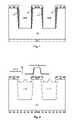
- FIGS. 1 and 2are each a cross-sectional side view of an illustrative semiconductor device without carbon-enriched trench sidewalls, during various steps of manufacturing.
- FIGS. 3-5are each a cross-sectional side view of an illustrative semiconductor device with carbon-enriched trench sidewalls, during various steps of manufacturing.
- the deviceincludes a substrate (not shown), such as silicon or silicon-on-oxide (SOI), over which a lower hardmask layer 102 may be disposed.
- Lower hardmask layer 102may be, for example, a nitride such as silicon carbon nitride (SiCN), or an oxide such as silicon dioxide (SiO2).
- One or more circuit elementsmay be disposed in and/or on the substrate and below lower hardmask layer 102 .
- At least one inter-layer dielectric (ILD) layer 101is disposed over insulating layer 102 .
- ILD 101is typically used to help electrically insulate circuit elements from each other and/or is the location where horizontal interconnects are run to electrically interconnect circuit elements.
- ILD 101may be made of any appropriate insulating material, such as hydrogenated silicon oxycarbide (SiCOH) or a material called SiLK semiconductor dielectric resin (a known material available from The Dow Chemical Company).
- An upper hardmask layer 103is disposed on ILD layer 101 .
- Upper hardmask layer 103may be the same as or a different material from lower hardmask layer 102 .
- Upper hardmask layer 103may be used to help prevent moisture from being absorbed by ILD 101 during the manufacturing process.
- Upper hardmask layer 103may also reduce or even prevent damage to ILD 101 during the subsequent lithography re-work process, which uses oxygen gas.
- ILD 101contains two trenches 104 A, 104 B, each extending lengthwise in a direction normal to the page on which FIG. 1 is shown and is used as a conductive interconnect line. Trenches 104 A, 104 B are separated from each other by a region of ILD 101 .
- Trenches 104 A, 104 Bare formed by etching, such as resistive ion etching (RIE), followed by a cleaning process, such as a wet cleaning process.
- etchingsuch as resistive ion etching (RIE)
- RIEresistive ion etching
- both upper hardmask 103 and ILD layer 101are etched.
- portions 105 of ILD layer 101are weakened during etching.
- weakened portions 105are damaged by destroying or changing the bonding between the molecules and the carbon atoms that were (at least previously) part of the molecules. When subsequent stripping of lithographic resist (not shown) is performed, these weakened portions 105 are partially or fully removed.
- a silicon layer 310is provided, which may be a substrate of the semiconductor device or disposed on another substrate, such as part of a silicon-on-oxide (SOI) structure. Circuit elements such as transistors and capacitors (not shown) may be formed on and/or in silicon layer 310 .
- Lower hardmask layer 102may be formed on (either directly on or indirectly on with layers in between) silicon layer 310 .
- another ILD layer(not shown) may be formed on the various circuit elements, and hardmask layer 102 may be formed on that other ILD layer.
- the terms “formed on” and “disposed on”are to be interpreted to include both directly formed/disposed on (i.e., immediately adjacent with no layers in between; physically touching) and indirectly formed/disposed on (with one or more layers in between).
- an anti-reflective coating (ARC) 304is formed on upper hardmask 103 in preparation for lithography. Then, a photosensitive etch resist layer 305 is formed on ARC 304 . The, resist layer 305 is patterned and partially removed through traditional lithographic processes to provide opening where trenches and/or other features are to be formed in underlying ILD 101 .
- ARCanti-reflective coating
- trenches in ILD layer 101are etched.
- trenches 401 A, 401 Bmay be etched using, for example, RIE and subsequent wet cleaning.
- each trench 401 A, 401 Bextends lengthwise in a direction normal to the page on which FIG. 4 is shown and is used as a conductive interconnect line.
- two parallel trenchesare shown, a single trench may be used or more than two trenches may be used, and multiple trenches may or may not be parallel.
- trenches 401 A, 401 Bmay be electrically isolated from each other or they may electrically connected to each other at one or more points.
- carbon atomsare made more available than normal during the etching process.
- CF, C4F8, and/or COare conventionally used to etch ILD.
- carbon-containing chemicalsmay be added in gaseous, liquid, or plasma form.
- Argon, CF4, and/or CHF3.These added chemicals each may be added at a flow rate of, for example, about 1000 sccm or less.
- CF4may be provided at a flow rate of at least 50 sccm, and/or CHF3 may be provided at a flow rate of at least 5 sccm.
- this carbon-enriching RIE stepmay be performed in an oxygen-deprived environment, preferably with substantially no oxygen at all begin available to the semiconductor device being etched. Thus, for example, CO would not be included.
- the ILD sidewalls of trenches 401 A, 401 Bcontain extra carbon atoms as compared with the surrounding ILD material. These extra carbon atoms may be freely embedded as separate molecules or may become part of the existing ILD molecules. The result may be that any given portion of ILD layer 101 near the trenches 401 A, 401 B is either etched or remains intact, but otherwise is not weakened much, if at all, by the etching process.
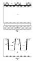
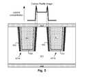
- FIG. 5shows an illustrative carbon profile image resulting from the process in connection with FIGS. 3 and 4 .
- the carbon concentrationis greater at the sidewalls of trenches 401 A, 401 B than in the surrounding ILD material.
- the trench sidewallshave a carbon concentration that is higher than the portion of ILD 101 that is disposed between trenches 401 A, 401 B.
- the carbon concentration of the sidewalls of trenches 104 A, 104 Bis lower than that of the portion of ILD layer 101 disposed between trenches 104 A, 104 B.
- the carbon profile imagemay be determined by, for example, slicing a cross section of the semiconductor device at one or more trenches and measuring carbon concentration along the cross section using electronic energy loss spectroscopy (EELS).
- EELSelectronic energy loss spectroscopy
- FIG. 5also indicates that, within each trench 401 A, 401 B, a metal barrier layer 402 may be formed that lines the sidewalls and/or bottom of the respective trench.
- Trenches 401 A, 401 Bmay also be filled with or otherwise contain a conductive material such as a metal 501 (e.g., copper).
- Barrier layer 402helps reduce migration of metal 501 out of the trench and into ILD layer 101 .
Landscapes
- Engineering & Computer Science (AREA)
- Power Engineering (AREA)
- General Physics & Mathematics (AREA)
- Condensed Matter Physics & Semiconductors (AREA)
- Computer Hardware Design (AREA)
- Microelectronics & Electronic Packaging (AREA)
- Physics & Mathematics (AREA)
- Manufacturing & Machinery (AREA)
- Chemical & Material Sciences (AREA)
- Chemical Kinetics & Catalysis (AREA)
- General Chemical & Material Sciences (AREA)
- Inorganic Chemistry (AREA)
- Internal Circuitry In Semiconductor Integrated Circuit Devices (AREA)
Abstract
Description
- During the manufacturing of many semiconductor devices, trenches are formed in a layer of material, and then the trenches are filled. For instance, trenches may be formed in the inter-layer dielectric (ILD), and those trenches may be filled with copper, thereby forming interconnect lines along the trenches.
- During manufacturing, a continuous hardmask layer is added on top of the ILD, and a patterned resist layer is formed over selected portions of the hardmask. Trenches are then etched through openings in the resist layer. The etching step causes both the exposed hardmask and exposed ILD to be etched, thereby forming a trench in the ILD. However, the ILD is typically more susceptible to etching than the hardmask. This is because ILD often made of a very low-K (e.g., K being 2.5 or less) porous material. Because of this, the trench is formed to be wider at its mouth than the corresponding opening in the hardmask, thereby forming an undercut under the hardmask. Such undercuts can reduce interconnect reliability in the finished product due to increased electro-migration and stress migration problems. This undercut problem has hindered manufacturers from forming interconnects in very low-K ILDs.
- Some manufacturers have attempted to avoid this problem by not using a hardmask over the ILD. However, there are problems with not using a hardmask, such as moisture absorption that affects the capacitances between various circuit elements in an unpredictable and undesirable manner.
- Accordingly, there is a need for a way to reduce, or even prevent, undercut of trenches in an inter-layer dielectric (ILD), while still using a hardmask over the ILD. It would be desirable to be able to reduce or prevent such hardmask undercut even where the ILD is a very low-K material that is very readily etched.
- To reduce or even prevent hardmask undercut, a carbon-rich layer is formed in the sidewalls of a trench in the ILD. This carbon-rich layer may protect the trench from being excessively etched. The carbon-rich layer may be formed simultaneously with and during the etching process, by increasing the amount of carbon available to be absorbed by the ILD during the trench etching process. The existence of the extra available carbon may slow the etching of the carbon-enriched regions of the ILD.
- These and other aspects of the disclosure will be apparent upon consideration of the following detailed description of illustrative embodiments.
- A more complete understanding of the present invention and the advantages thereof may be acquired by referring to the following description in consideration of the accompanying drawings, in which like reference numbers indicate like features, and wherein:
FIGS. 1 and 2 are each a cross-sectional side view of an illustrative semiconductor device without carbon-enriched trench sidewalls, during various steps of manufacturing.FIGS. 3-5 are each a cross-sectional side view of an illustrative semiconductor device with carbon-enriched trench sidewalls, during various steps of manufacturing.- Referring to
FIG. 1 , a cross-sectional side view of at least a portion of a semiconductor device is shown. The device includes a substrate (not shown), such as silicon or silicon-on-oxide (SOI), over which alower hardmask layer 102 may be disposed.Lower hardmask layer 102 may be, for example, a nitride such as silicon carbon nitride (SiCN), or an oxide such as silicon dioxide (SiO2). One or more circuit elements (not shown) may be disposed in and/or on the substrate and belowlower hardmask layer 102. At least one inter-layer dielectric (ILD)layer 101 is disposed overinsulating layer 102. An ILD is typically used to help electrically insulate circuit elements from each other and/or is the location where horizontal interconnects are run to electrically interconnect circuit elements. ILD101 may be made of any appropriate insulating material, such as hydrogenated silicon oxycarbide (SiCOH) or a material called SiLK semiconductor dielectric resin (a known material available from The Dow Chemical Company). - An
upper hardmask layer 103 is disposed onILD layer 101.Upper hardmask layer 103 may be the same as or a different material fromlower hardmask layer 102.Upper hardmask layer 103 may be used to help prevent moisture from being absorbed by ILD101 during the manufacturing process.Upper hardmask layer 103 may also reduce or even prevent damage to ILD101 during the subsequent lithography re-work process, which uses oxygen gas. - In
FIG. 1 , ILD101 contains twotrenches FIG. 1 is shown and is used as a conductive interconnect line. Trenches104A,104B are separated from each other by a region of ILD101. Trenches trenches upper hardmask 103 and ILDlayer 101 are etched. However, since ILDlayer 101 is more readily etched thanhardmask layer 103,portions 105 ofILD layer 101 are weakened during etching. In particular, weakenedportions 105 are damaged by destroying or changing the bonding between the molecules and the carbon atoms that were (at least previously) part of the molecules. When subsequent stripping of lithographic resist (not shown) is performed, these weakenedportions 105 are partially or fully removed. This results in the opening etched inILD layer 101 that forms eachtrench upper hardmask layer 103. Accordingly, referring toFIG. 2 , anundercut 201 underupper hardmask layer 103 is formed during the resist stripping step. This is undesirable as it can reduce interconnect reliability in the finished product due to increased electro-migration and stress migration problems.- Thus, an illustrative manufacturing method is now described that can reduce or even prevent such an undercut. Referring to
FIG. 3 , a silicon layer310 is provided, which may be a substrate of the semiconductor device or disposed on another substrate, such as part of a silicon-on-oxide (SOI) structure. Circuit elements such as transistors and capacitors (not shown) may be formed on and/or in silicon layer310. Lower hardmask layer 102 may be formed on (either directly on or indirectly on with layers in between) silicon layer310. For instance, another ILD layer (not shown) may be formed on the various circuit elements, andhardmask layer 102 may be formed on that other ILD layer. The terms “formed on” and “disposed on” are to be interpreted to include both directly formed/disposed on (i.e., immediately adjacent with no layers in between; physically touching) and indirectly formed/disposed on (with one or more layers in between).- Next, an anti-reflective coating (ARC)304 is formed on
upper hardmask 103 in preparation for lithography. Then, a photosensitiveetch resist layer 305 is formed onARC 304. The,resist layer 305 is patterned and partially removed through traditional lithographic processes to provide opening where trenches and/or other features are to be formed in underlying ILD101. - Once the layers as shown in
FIG. 3 are formed or otherwise provided, trenches in ILDlayer 101 are etched. Referring toFIG. 4 ,trenches trench FIG. 4 is shown and is used as a conductive interconnect line. Although two parallel trenches are shown, a single trench may be used or more than two trenches may be used, and multiple trenches may or may not be parallel. Also,trenches - However, unlike in
FIG. 2 , in this example there is little or no undercut in ILD100 at the point where ILD100 andupper hardmask layer 103 meet. This is because carbon enrichment of the sidewalls oftrenches portions 402. As shown inFIG. 4 , portions ofupper hardmask 103 may also be carbon enriched. By enriching the trench sidewalls with extra carbon, this helps to reduce or even prevent the above-discussed damage to the trench sidewalls that typically occurs during trench etching. Thus, the undercut problem may be reduced or even avoided, even whereILD layer 101 has a very low K such as 2.5 or less. - To achieve carbon enrichment, carbon atoms are made more available than normal during the etching process. For instance, during traditional RIE, CF, C4F8, and/or CO are conventionally used to etch ILD. However, to provide for carbon enrichment of trench sidewalls, carbon-containing chemicals may be added in gaseous, liquid, or plasma form. For example, the following may be added to the etching chemicals: Argon, CF4, and/or CHF3. These added chemicals each may be added at a flow rate of, for example, about 1000 sccm or less. In some illustrative embodiments, CF4 may be provided at a flow rate of at least 50 sccm, and/or CHF3 may be provided at a flow rate of at least 5 sccm. Moreover, this carbon-enriching RIE step may be performed in an oxygen-deprived environment, preferably with substantially no oxygen at all begin available to the semiconductor device being etched. Thus, for example, CO would not be included.
- Thus, during the etching process, while the
trenches ILD layer 101, replacing the carbon that would otherwise be lost or modified during a traditional etching step. Thus, the ILD sidewalls oftrenches ILD layer 101 near thetrenches FIG. 5 shows an illustrative carbon profile image resulting from the process in connection withFIGS. 3 and 4 . As can be seen, the carbon concentration is greater at the sidewalls oftrenches ILD 101 that is disposed betweentrenches FIG. 2 , the carbon concentration of the sidewalls oftrenches ILD layer 101 disposed betweentrenches FIG. 5 also indicates that, within eachtrench metal barrier layer 402 may be formed that lines the sidewalls and/or bottom of the respective trench.Trenches Barrier layer 402 helps reduce migration ofmetal 501 out of the trench and intoILD layer 101.- Thus, a way of reducing or even preventing hardmask undercut in an ILD trench of a semiconductor device has been described, by forming a carbon-rich layer in the sidewalls of the trench during trench etching.
Claims (16)
1. A semiconductor device, comprising:
a silicon layer; and
a dielectric layer disposed on the silicon layer and having a first trench and a second trench disposed such that a region of the dielectric layer exists between the first and second trenches, wherein the first and second trench each contains a metal and has a sidewall having a carbon concentration higher than a carbon concentration of the region of the dielectric layer.
2. The semiconductor device ofclaim 1 , further including a first silicon carbon nitride layer disposed on the region of the dielectric layer.
3. The semiconductor device ofclaim 2 , further including a second silicon carbon nitride layer disposed between the silicon layer and the dielectric layer.
4. The semiconductor device ofclaim 1 , wherein the dielectric layer has a K that is less than or equal to 2.5.
5. The semiconductor device ofclaim 1 , wherein the dielectric layer is hydrogenated silicon oxycarbide (SiCOH)
6. The semiconductor device ofclaim 1 , wherein the dielectric layer is SiLK semiconductor dielectric resin.
7. The semiconductor device ofclaim 1 , wherein the metal is copper.
8. The semiconductor device ofclaim 1 , wherein the trench is filled with the metal.
9. A method for manufacturing a semiconductor device, comprising:
providing a silicon layer with a dielectric layer disposed on the silicon layer;
etching a first trench in the dielectric layer such that a carbon concentration of a sidewall of the first trench has a carbon concentration higher than a region of the dielectric layer; and
forming a metal layer in the first trench.
10. The method ofclaim 9 , further including forming a silicon carbon nitride layer on the dielectric layer including the region of the dielectric layer prior to the step of etching the first trench, such that the step of etching includes etching the silicon carbon nitride layer.
11. The method ofclaim 9 , wherein the step of etching further includes etching a second trench in the dielectric layer separated from the first trench by the region of the dielectric layer, such that the second trench also has a sidewall having a carbon concentration higher than the region of the dielectric layer.
12. The method ofclaim 9 , wherein the step of etching includes performing reactive ion etching with carbon enrichment.
13. The method ofclaim 12 , wherein the step of etching includes applying CH4 at a flow rate of at least 50 sccm.
14. The method ofclaim 12 , wherein the step of etching includes applying CHF3 at a flow rate of at least 5 sccm.
15. The method ofclaim 12 , wherein the step of etching is performed in an environment having substantially no oxygen.
16. The method ofclaim 9 , further including:
forming a resist layer on the dielectric layer prior to the step of etching, wherein the resist layer is resistant to the step of etching; and
removing the resist layer after the step of etching.
Priority Applications (2)
| Application Number | Priority Date | Filing Date | Title |
|---|---|---|---|
| US12/013,683US8018023B2 (en) | 2008-01-14 | 2008-01-14 | Trench sidewall protection by a carbon-rich layer in a semiconductor device |
| JP2008330642AJP2009170901A (en) | 2008-01-14 | 2008-12-25 | Trench sidewall protection by carbon rich layers in semiconductor devices. |
Applications Claiming Priority (1)
| Application Number | Priority Date | Filing Date | Title |
|---|---|---|---|
| US12/013,683US8018023B2 (en) | 2008-01-14 | 2008-01-14 | Trench sidewall protection by a carbon-rich layer in a semiconductor device |
Publications (2)
| Publication Number | Publication Date |
|---|---|
| US20090179300A1true US20090179300A1 (en) | 2009-07-16 |
| US8018023B2 US8018023B2 (en) | 2011-09-13 |
Family
ID=40849913
Family Applications (1)
| Application Number | Title | Priority Date | Filing Date |
|---|---|---|---|
| US12/013,683Expired - Fee RelatedUS8018023B2 (en) | 2008-01-14 | 2008-01-14 | Trench sidewall protection by a carbon-rich layer in a semiconductor device |
Country Status (2)
| Country | Link |
|---|---|
| US (1) | US8018023B2 (en) |
| JP (1) | JP2009170901A (en) |
Cited By (127)
| Publication number | Priority date | Publication date | Assignee | Title |
|---|---|---|---|---|
| WO2014046858A1 (en)* | 2012-09-20 | 2014-03-27 | Applied Materials, Inc. | Silicon-carbon-nitride selective etch |
| US9287134B2 (en) | 2014-01-17 | 2016-03-15 | Applied Materials, Inc. | Titanium oxide etch |
| US9287095B2 (en) | 2013-12-17 | 2016-03-15 | Applied Materials, Inc. | Semiconductor system assemblies and methods of operation |
| US9293568B2 (en) | 2014-01-27 | 2016-03-22 | Applied Materials, Inc. | Method of fin patterning |
| US9299575B2 (en) | 2014-03-17 | 2016-03-29 | Applied Materials, Inc. | Gas-phase tungsten etch |
| US9299537B2 (en) | 2014-03-20 | 2016-03-29 | Applied Materials, Inc. | Radial waveguide systems and methods for post-match control of microwaves |
| US9299583B1 (en) | 2014-12-05 | 2016-03-29 | Applied Materials, Inc. | Aluminum oxide selective etch |
| US9309598B2 (en) | 2014-05-28 | 2016-04-12 | Applied Materials, Inc. | Oxide and metal removal |
| US9324576B2 (en) | 2010-05-27 | 2016-04-26 | Applied Materials, Inc. | Selective etch for silicon films |
| US9343272B1 (en) | 2015-01-08 | 2016-05-17 | Applied Materials, Inc. | Self-aligned process |
| US9349605B1 (en) | 2015-08-07 | 2016-05-24 | Applied Materials, Inc. | Oxide etch selectivity systems and methods |
| US9355863B2 (en) | 2012-12-18 | 2016-05-31 | Applied Materials, Inc. | Non-local plasma oxide etch |
| US9355862B2 (en) | 2014-09-24 | 2016-05-31 | Applied Materials, Inc. | Fluorine-based hardmask removal |
| US9355856B2 (en) | 2014-09-12 | 2016-05-31 | Applied Materials, Inc. | V trench dry etch |
| CN105633006A (en)* | 2014-10-30 | 2016-06-01 | 中芯国际集成电路制造(上海)有限公司 | Interconnection structure and manufacturing method therefor |
| US9362130B2 (en) | 2013-03-01 | 2016-06-07 | Applied Materials, Inc. | Enhanced etching processes using remote plasma sources |
| US9368364B2 (en) | 2014-09-24 | 2016-06-14 | Applied Materials, Inc. | Silicon etch process with tunable selectivity to SiO2 and other materials |
| US9373522B1 (en) | 2015-01-22 | 2016-06-21 | Applied Mateials, Inc. | Titanium nitride removal |
| US9373517B2 (en) | 2012-08-02 | 2016-06-21 | Applied Materials, Inc. | Semiconductor processing with DC assisted RF power for improved control |
| US9378969B2 (en) | 2014-06-19 | 2016-06-28 | Applied Materials, Inc. | Low temperature gas-phase carbon removal |
| US9378978B2 (en) | 2014-07-31 | 2016-06-28 | Applied Materials, Inc. | Integrated oxide recess and floating gate fin trimming |
| US9385028B2 (en) | 2014-02-03 | 2016-07-05 | Applied Materials, Inc. | Air gap process |
| US9384997B2 (en) | 2012-11-20 | 2016-07-05 | Applied Materials, Inc. | Dry-etch selectivity |
| US9396989B2 (en) | 2014-01-27 | 2016-07-19 | Applied Materials, Inc. | Air gaps between copper lines |
| US9406523B2 (en) | 2014-06-19 | 2016-08-02 | Applied Materials, Inc. | Highly selective doped oxide removal method |
| US9412608B2 (en) | 2012-11-30 | 2016-08-09 | Applied Materials, Inc. | Dry-etch for selective tungsten removal |
| US9418858B2 (en) | 2011-10-07 | 2016-08-16 | Applied Materials, Inc. | Selective etch of silicon by way of metastable hydrogen termination |
| US9425058B2 (en) | 2014-07-24 | 2016-08-23 | Applied Materials, Inc. | Simplified litho-etch-litho-etch process |
| US9437451B2 (en) | 2012-09-18 | 2016-09-06 | Applied Materials, Inc. | Radical-component oxide etch |
| US9449850B2 (en) | 2013-03-15 | 2016-09-20 | Applied Materials, Inc. | Processing systems and methods for halide scavenging |
| US9449845B2 (en) | 2012-12-21 | 2016-09-20 | Applied Materials, Inc. | Selective titanium nitride etching |
| US9449846B2 (en) | 2015-01-28 | 2016-09-20 | Applied Materials, Inc. | Vertical gate separation |
| US9472412B2 (en) | 2013-12-02 | 2016-10-18 | Applied Materials, Inc. | Procedure for etch rate consistency |
| US9472417B2 (en) | 2013-11-12 | 2016-10-18 | Applied Materials, Inc. | Plasma-free metal etch |
| US9478432B2 (en) | 2014-09-25 | 2016-10-25 | Applied Materials, Inc. | Silicon oxide selective removal |
| US9496167B2 (en) | 2014-07-31 | 2016-11-15 | Applied Materials, Inc. | Integrated bit-line airgap formation and gate stack post clean |
| US9493879B2 (en) | 2013-07-12 | 2016-11-15 | Applied Materials, Inc. | Selective sputtering for pattern transfer |
| US9502258B2 (en) | 2014-12-23 | 2016-11-22 | Applied Materials, Inc. | Anisotropic gap etch |
| US9499898B2 (en) | 2014-03-03 | 2016-11-22 | Applied Materials, Inc. | Layered thin film heater and method of fabrication |
| US9553102B2 (en) | 2014-08-19 | 2017-01-24 | Applied Materials, Inc. | Tungsten separation |
| US9576809B2 (en) | 2013-11-04 | 2017-02-21 | Applied Materials, Inc. | Etch suppression with germanium |
| US9607856B2 (en) | 2013-03-05 | 2017-03-28 | Applied Materials, Inc. | Selective titanium nitride removal |
| US9659753B2 (en) | 2014-08-07 | 2017-05-23 | Applied Materials, Inc. | Grooved insulator to reduce leakage current |
| US9691645B2 (en) | 2015-08-06 | 2017-06-27 | Applied Materials, Inc. | Bolted wafer chuck thermal management systems and methods for wafer processing systems |
| US9721789B1 (en) | 2016-10-04 | 2017-08-01 | Applied Materials, Inc. | Saving ion-damaged spacers |
| US9728437B2 (en) | 2015-02-03 | 2017-08-08 | Applied Materials, Inc. | High temperature chuck for plasma processing systems |
| US9741593B2 (en) | 2015-08-06 | 2017-08-22 | Applied Materials, Inc. | Thermal management systems and methods for wafer processing systems |
| US9768034B1 (en) | 2016-11-11 | 2017-09-19 | Applied Materials, Inc. | Removal methods for high aspect ratio structures |
| US9773648B2 (en) | 2013-08-30 | 2017-09-26 | Applied Materials, Inc. | Dual discharge modes operation for remote plasma |
| US9842744B2 (en) | 2011-03-14 | 2017-12-12 | Applied Materials, Inc. | Methods for etch of SiN films |
| US9865484B1 (en) | 2016-06-29 | 2018-01-09 | Applied Materials, Inc. | Selective etch using material modification and RF pulsing |
| US9881805B2 (en) | 2015-03-02 | 2018-01-30 | Applied Materials, Inc. | Silicon selective removal |
| US9885117B2 (en) | 2014-03-31 | 2018-02-06 | Applied Materials, Inc. | Conditioned semiconductor system parts |
| US9887096B2 (en) | 2012-09-17 | 2018-02-06 | Applied Materials, Inc. | Differential silicon oxide etch |
| US9934942B1 (en) | 2016-10-04 | 2018-04-03 | Applied Materials, Inc. | Chamber with flow-through source |
| US9947549B1 (en) | 2016-10-10 | 2018-04-17 | Applied Materials, Inc. | Cobalt-containing material removal |
| US9978564B2 (en) | 2012-09-21 | 2018-05-22 | Applied Materials, Inc. | Chemical control features in wafer process equipment |
| US10026621B2 (en) | 2016-11-14 | 2018-07-17 | Applied Materials, Inc. | SiN spacer profile patterning |
| US10043674B1 (en) | 2017-08-04 | 2018-08-07 | Applied Materials, Inc. | Germanium etching systems and methods |
| US10043684B1 (en) | 2017-02-06 | 2018-08-07 | Applied Materials, Inc. | Self-limiting atomic thermal etching systems and methods |
| US10049891B1 (en) | 2017-05-31 | 2018-08-14 | Applied Materials, Inc. | Selective in situ cobalt residue removal |
| US10062575B2 (en) | 2016-09-09 | 2018-08-28 | Applied Materials, Inc. | Poly directional etch by oxidation |
| US10062585B2 (en) | 2016-10-04 | 2018-08-28 | Applied Materials, Inc. | Oxygen compatible plasma source |
| US10062578B2 (en) | 2011-03-14 | 2018-08-28 | Applied Materials, Inc. | Methods for etch of metal and metal-oxide films |
| US10062579B2 (en) | 2016-10-07 | 2018-08-28 | Applied Materials, Inc. | Selective SiN lateral recess |
| US10062587B2 (en) | 2012-07-18 | 2018-08-28 | Applied Materials, Inc. | Pedestal with multi-zone temperature control and multiple purge capabilities |
| US10128086B1 (en) | 2017-10-24 | 2018-11-13 | Applied Materials, Inc. | Silicon pretreatment for nitride removal |
| US10163696B2 (en) | 2016-11-11 | 2018-12-25 | Applied Materials, Inc. | Selective cobalt removal for bottom up gapfill |
| US10170336B1 (en) | 2017-08-04 | 2019-01-01 | Applied Materials, Inc. | Methods for anisotropic control of selective silicon removal |
| US10224210B2 (en) | 2014-12-09 | 2019-03-05 | Applied Materials, Inc. | Plasma processing system with direct outlet toroidal plasma source |
| US10242908B2 (en) | 2016-11-14 | 2019-03-26 | Applied Materials, Inc. | Airgap formation with damage-free copper |
| US10256112B1 (en) | 2017-12-08 | 2019-04-09 | Applied Materials, Inc. | Selective tungsten removal |
| US10256079B2 (en) | 2013-02-08 | 2019-04-09 | Applied Materials, Inc. | Semiconductor processing systems having multiple plasma configurations |
| US10283321B2 (en) | 2011-01-18 | 2019-05-07 | Applied Materials, Inc. | Semiconductor processing system and methods using capacitively coupled plasma |
| US10283324B1 (en) | 2017-10-24 | 2019-05-07 | Applied Materials, Inc. | Oxygen treatment for nitride etching |
| US10297458B2 (en) | 2017-08-07 | 2019-05-21 | Applied Materials, Inc. | Process window widening using coated parts in plasma etch processes |
| US10319600B1 (en) | 2018-03-12 | 2019-06-11 | Applied Materials, Inc. | Thermal silicon etch |
| US10319739B2 (en) | 2017-02-08 | 2019-06-11 | Applied Materials, Inc. | Accommodating imperfectly aligned memory holes |
| US10319649B2 (en) | 2017-04-11 | 2019-06-11 | Applied Materials, Inc. | Optical emission spectroscopy (OES) for remote plasma monitoring |
| US10354889B2 (en) | 2017-07-17 | 2019-07-16 | Applied Materials, Inc. | Non-halogen etching of silicon-containing materials |
| US10403507B2 (en) | 2017-02-03 | 2019-09-03 | Applied Materials, Inc. | Shaped etch profile with oxidation |
| US10431429B2 (en) | 2017-02-03 | 2019-10-01 | Applied Materials, Inc. | Systems and methods for radial and azimuthal control of plasma uniformity |
| US10468267B2 (en) | 2017-05-31 | 2019-11-05 | Applied Materials, Inc. | Water-free etching methods |
| US10490418B2 (en) | 2014-10-14 | 2019-11-26 | Applied Materials, Inc. | Systems and methods for internal surface conditioning assessment in plasma processing equipment |
| US10490406B2 (en) | 2018-04-10 | 2019-11-26 | Appled Materials, Inc. | Systems and methods for material breakthrough |
| US10497573B2 (en) | 2018-03-13 | 2019-12-03 | Applied Materials, Inc. | Selective atomic layer etching of semiconductor materials |
| US10504700B2 (en) | 2015-08-27 | 2019-12-10 | Applied Materials, Inc. | Plasma etching systems and methods with secondary plasma injection |
| US10504754B2 (en) | 2016-05-19 | 2019-12-10 | Applied Materials, Inc. | Systems and methods for improved semiconductor etching and component protection |
| US10522371B2 (en) | 2016-05-19 | 2019-12-31 | Applied Materials, Inc. | Systems and methods for improved semiconductor etching and component protection |
| US10541246B2 (en) | 2017-06-26 | 2020-01-21 | Applied Materials, Inc. | 3D flash memory cells which discourage cross-cell electrical tunneling |
| US10541184B2 (en) | 2017-07-11 | 2020-01-21 | Applied Materials, Inc. | Optical emission spectroscopic techniques for monitoring etching |
| US10546729B2 (en) | 2016-10-04 | 2020-01-28 | Applied Materials, Inc. | Dual-channel showerhead with improved profile |
| US10566206B2 (en) | 2016-12-27 | 2020-02-18 | Applied Materials, Inc. | Systems and methods for anisotropic material breakthrough |
| US10573496B2 (en) | 2014-12-09 | 2020-02-25 | Applied Materials, Inc. | Direct outlet toroidal plasma source |
| US10573527B2 (en) | 2018-04-06 | 2020-02-25 | Applied Materials, Inc. | Gas-phase selective etching systems and methods |
| US10593560B2 (en) | 2018-03-01 | 2020-03-17 | Applied Materials, Inc. | Magnetic induction plasma source for semiconductor processes and equipment |
| US10593523B2 (en) | 2014-10-14 | 2020-03-17 | Applied Materials, Inc. | Systems and methods for internal surface conditioning in plasma processing equipment |
| US10615047B2 (en) | 2018-02-28 | 2020-04-07 | Applied Materials, Inc. | Systems and methods to form airgaps |
| US10629473B2 (en) | 2016-09-09 | 2020-04-21 | Applied Materials, Inc. | Footing removal for nitride spacer |
| US10672642B2 (en) | 2018-07-24 | 2020-06-02 | Applied Materials, Inc. | Systems and methods for pedestal configuration |
| US10679870B2 (en) | 2018-02-15 | 2020-06-09 | Applied Materials, Inc. | Semiconductor processing chamber multistage mixing apparatus |
| US10699879B2 (en) | 2018-04-17 | 2020-06-30 | Applied Materials, Inc. | Two piece electrode assembly with gap for plasma control |
| US10727080B2 (en) | 2017-07-07 | 2020-07-28 | Applied Materials, Inc. | Tantalum-containing material removal |
| US10755941B2 (en) | 2018-07-06 | 2020-08-25 | Applied Materials, Inc. | Self-limiting selective etching systems and methods |
| US10854426B2 (en) | 2018-01-08 | 2020-12-01 | Applied Materials, Inc. | Metal recess for semiconductor structures |
| US10872778B2 (en) | 2018-07-06 | 2020-12-22 | Applied Materials, Inc. | Systems and methods utilizing solid-phase etchants |
| US10886137B2 (en) | 2018-04-30 | 2021-01-05 | Applied Materials, Inc. | Selective nitride removal |
| US10892198B2 (en) | 2018-09-14 | 2021-01-12 | Applied Materials, Inc. | Systems and methods for improved performance in semiconductor processing |
| US10903054B2 (en) | 2017-12-19 | 2021-01-26 | Applied Materials, Inc. | Multi-zone gas distribution systems and methods |
| US10920320B2 (en) | 2017-06-16 | 2021-02-16 | Applied Materials, Inc. | Plasma health determination in semiconductor substrate processing reactors |
| US10920319B2 (en) | 2019-01-11 | 2021-02-16 | Applied Materials, Inc. | Ceramic showerheads with conductive electrodes |
| US10943834B2 (en) | 2017-03-13 | 2021-03-09 | Applied Materials, Inc. | Replacement contact process |
| US10964512B2 (en) | 2018-02-15 | 2021-03-30 | Applied Materials, Inc. | Semiconductor processing chamber multistage mixing apparatus and methods |
| US11049755B2 (en) | 2018-09-14 | 2021-06-29 | Applied Materials, Inc. | Semiconductor substrate supports with embedded RF shield |
| US11062887B2 (en) | 2018-09-17 | 2021-07-13 | Applied Materials, Inc. | High temperature RF heater pedestals |
| US11121002B2 (en) | 2018-10-24 | 2021-09-14 | Applied Materials, Inc. | Systems and methods for etching metals and metal derivatives |
| US11239061B2 (en) | 2014-11-26 | 2022-02-01 | Applied Materials, Inc. | Methods and systems to enhance process uniformity |
| US11257693B2 (en) | 2015-01-09 | 2022-02-22 | Applied Materials, Inc. | Methods and systems to improve pedestal temperature control |
| US11276559B2 (en) | 2017-05-17 | 2022-03-15 | Applied Materials, Inc. | Semiconductor processing chamber for multiple precursor flow |
| US11276590B2 (en) | 2017-05-17 | 2022-03-15 | Applied Materials, Inc. | Multi-zone semiconductor substrate supports |
| US11328909B2 (en) | 2017-12-22 | 2022-05-10 | Applied Materials, Inc. | Chamber conditioning and removal processes |
| US11417534B2 (en) | 2018-09-21 | 2022-08-16 | Applied Materials, Inc. | Selective material removal |
| US11437242B2 (en) | 2018-11-27 | 2022-09-06 | Applied Materials, Inc. | Selective removal of silicon-containing materials |
| US11594428B2 (en) | 2015-02-03 | 2023-02-28 | Applied Materials, Inc. | Low temperature chuck for plasma processing systems |
| US11682560B2 (en) | 2018-10-11 | 2023-06-20 | Applied Materials, Inc. | Systems and methods for hafnium-containing film removal |
| US11721527B2 (en) | 2019-01-07 | 2023-08-08 | Applied Materials, Inc. | Processing chamber mixing systems |
| US12340979B2 (en) | 2017-05-17 | 2025-06-24 | Applied Materials, Inc. | Semiconductor processing chamber for improved precursor flow |
Families Citing this family (2)
| Publication number | Priority date | Publication date | Assignee | Title |
|---|---|---|---|---|
| US8646168B2 (en)* | 2011-09-30 | 2014-02-11 | HGST Netherlands B.V. | Method for manufacturing a magnetic write pole of a perpendicular magnetic write head using novel mask fabrication |
| US10020239B2 (en)* | 2016-01-12 | 2018-07-10 | Taiwan Semiconductor Manufacturing Company Ltd. | Semiconductor structure and manufacturing method thereof |
Citations (3)
| Publication number | Priority date | Publication date | Assignee | Title |
|---|---|---|---|---|
| US20070232062A1 (en)* | 2006-03-31 | 2007-10-04 | Takeshi Nogami | Damascene interconnection having porous low k layer followed by a nonporous low k layer |
| US20090072401A1 (en)* | 2007-09-19 | 2009-03-19 | International Business Machines Corporation | Methods to mitigate plasma damage in organosilicate dielectrics using a protective sidewall spacer |
| US20090160061A1 (en)* | 2007-12-21 | 2009-06-25 | Taiwan Semiconductor Manufacturing Company, Ltd. | Introducing a Metal Layer Between Sin and Tin to Improve CBD Contact Resistance for P-TSV |
Family Cites Families (8)
| Publication number | Priority date | Publication date | Assignee | Title |
|---|---|---|---|---|
| US6821884B2 (en) | 2001-02-15 | 2004-11-23 | Interuniversitair Microelektronica Centrum (Imec) | Method of fabricating a semiconductor device |
| JP2003092287A (en) | 2001-09-19 | 2003-03-28 | Nec Corp | Ashing method |
| KR100419746B1 (en) | 2002-01-09 | 2004-02-25 | 주식회사 하이닉스반도체 | A method for manufacturing a multi-layer metal line of a semiconductor device |
| WO2003083935A1 (en) | 2002-04-03 | 2003-10-09 | Nec Corporation | Semiconductor device and its manufacturing method |
| JP3717073B2 (en) | 2002-12-24 | 2005-11-16 | 株式会社ルネサステクノロジ | Manufacturing method of semiconductor device |
| JP3676784B2 (en) | 2003-01-28 | 2005-07-27 | Necエレクトロニクス株式会社 | Semiconductor device and manufacturing method thereof |
| JP2005197606A (en) | 2004-01-09 | 2005-07-21 | Toshiba Corp | Semiconductor device and manufacturing method thereof |
| JP2005217371A (en) | 2004-02-02 | 2005-08-11 | Matsushita Electric Ind Co Ltd | Semiconductor device and manufacturing method thereof |
- 2008
- 2008-01-14USUS12/013,683patent/US8018023B2/ennot_activeExpired - Fee Related
- 2008-12-25JPJP2008330642Apatent/JP2009170901A/enactivePending
Patent Citations (3)
| Publication number | Priority date | Publication date | Assignee | Title |
|---|---|---|---|---|
| US20070232062A1 (en)* | 2006-03-31 | 2007-10-04 | Takeshi Nogami | Damascene interconnection having porous low k layer followed by a nonporous low k layer |
| US20090072401A1 (en)* | 2007-09-19 | 2009-03-19 | International Business Machines Corporation | Methods to mitigate plasma damage in organosilicate dielectrics using a protective sidewall spacer |
| US20090160061A1 (en)* | 2007-12-21 | 2009-06-25 | Taiwan Semiconductor Manufacturing Company, Ltd. | Introducing a Metal Layer Between Sin and Tin to Improve CBD Contact Resistance for P-TSV |
Cited By (179)
| Publication number | Priority date | Publication date | Assignee | Title |
|---|---|---|---|---|
| US9324576B2 (en) | 2010-05-27 | 2016-04-26 | Applied Materials, Inc. | Selective etch for silicon films |
| US9754800B2 (en) | 2010-05-27 | 2017-09-05 | Applied Materials, Inc. | Selective etch for silicon films |
| US10283321B2 (en) | 2011-01-18 | 2019-05-07 | Applied Materials, Inc. | Semiconductor processing system and methods using capacitively coupled plasma |
| US9842744B2 (en) | 2011-03-14 | 2017-12-12 | Applied Materials, Inc. | Methods for etch of SiN films |
| US10062578B2 (en) | 2011-03-14 | 2018-08-28 | Applied Materials, Inc. | Methods for etch of metal and metal-oxide films |
| US9418858B2 (en) | 2011-10-07 | 2016-08-16 | Applied Materials, Inc. | Selective etch of silicon by way of metastable hydrogen termination |
| US10062587B2 (en) | 2012-07-18 | 2018-08-28 | Applied Materials, Inc. | Pedestal with multi-zone temperature control and multiple purge capabilities |
| US9373517B2 (en) | 2012-08-02 | 2016-06-21 | Applied Materials, Inc. | Semiconductor processing with DC assisted RF power for improved control |
| US10032606B2 (en) | 2012-08-02 | 2018-07-24 | Applied Materials, Inc. | Semiconductor processing with DC assisted RF power for improved control |
| US9887096B2 (en) | 2012-09-17 | 2018-02-06 | Applied Materials, Inc. | Differential silicon oxide etch |
| US9437451B2 (en) | 2012-09-18 | 2016-09-06 | Applied Materials, Inc. | Radical-component oxide etch |
| WO2014046858A1 (en)* | 2012-09-20 | 2014-03-27 | Applied Materials, Inc. | Silicon-carbon-nitride selective etch |
| US9390937B2 (en) | 2012-09-20 | 2016-07-12 | Applied Materials, Inc. | Silicon-carbon-nitride selective etch |
| US11264213B2 (en) | 2012-09-21 | 2022-03-01 | Applied Materials, Inc. | Chemical control features in wafer process equipment |
| US9978564B2 (en) | 2012-09-21 | 2018-05-22 | Applied Materials, Inc. | Chemical control features in wafer process equipment |
| US10354843B2 (en) | 2012-09-21 | 2019-07-16 | Applied Materials, Inc. | Chemical control features in wafer process equipment |
| US9384997B2 (en) | 2012-11-20 | 2016-07-05 | Applied Materials, Inc. | Dry-etch selectivity |
| US9412608B2 (en) | 2012-11-30 | 2016-08-09 | Applied Materials, Inc. | Dry-etch for selective tungsten removal |
| US9355863B2 (en) | 2012-12-18 | 2016-05-31 | Applied Materials, Inc. | Non-local plasma oxide etch |
| US9449845B2 (en) | 2012-12-21 | 2016-09-20 | Applied Materials, Inc. | Selective titanium nitride etching |
| US11024486B2 (en) | 2013-02-08 | 2021-06-01 | Applied Materials, Inc. | Semiconductor processing systems having multiple plasma configurations |
| US10256079B2 (en) | 2013-02-08 | 2019-04-09 | Applied Materials, Inc. | Semiconductor processing systems having multiple plasma configurations |
| US9362130B2 (en) | 2013-03-01 | 2016-06-07 | Applied Materials, Inc. | Enhanced etching processes using remote plasma sources |
| US10424485B2 (en) | 2013-03-01 | 2019-09-24 | Applied Materials, Inc. | Enhanced etching processes using remote plasma sources |
| US9607856B2 (en) | 2013-03-05 | 2017-03-28 | Applied Materials, Inc. | Selective titanium nitride removal |
| US9449850B2 (en) | 2013-03-15 | 2016-09-20 | Applied Materials, Inc. | Processing systems and methods for halide scavenging |
| US9704723B2 (en) | 2013-03-15 | 2017-07-11 | Applied Materials, Inc. | Processing systems and methods for halide scavenging |
| US9659792B2 (en) | 2013-03-15 | 2017-05-23 | Applied Materials, Inc. | Processing systems and methods for halide scavenging |
| US9493879B2 (en) | 2013-07-12 | 2016-11-15 | Applied Materials, Inc. | Selective sputtering for pattern transfer |
| US9773648B2 (en) | 2013-08-30 | 2017-09-26 | Applied Materials, Inc. | Dual discharge modes operation for remote plasma |
| US9576809B2 (en) | 2013-11-04 | 2017-02-21 | Applied Materials, Inc. | Etch suppression with germanium |
| US9472417B2 (en) | 2013-11-12 | 2016-10-18 | Applied Materials, Inc. | Plasma-free metal etch |
| US9711366B2 (en) | 2013-11-12 | 2017-07-18 | Applied Materials, Inc. | Selective etch for metal-containing materials |
| US9520303B2 (en) | 2013-11-12 | 2016-12-13 | Applied Materials, Inc. | Aluminum selective etch |
| US9472412B2 (en) | 2013-12-02 | 2016-10-18 | Applied Materials, Inc. | Procedure for etch rate consistency |
| US9287095B2 (en) | 2013-12-17 | 2016-03-15 | Applied Materials, Inc. | Semiconductor system assemblies and methods of operation |
| US9287134B2 (en) | 2014-01-17 | 2016-03-15 | Applied Materials, Inc. | Titanium oxide etch |
| US9396989B2 (en) | 2014-01-27 | 2016-07-19 | Applied Materials, Inc. | Air gaps between copper lines |
| US9293568B2 (en) | 2014-01-27 | 2016-03-22 | Applied Materials, Inc. | Method of fin patterning |
| US9385028B2 (en) | 2014-02-03 | 2016-07-05 | Applied Materials, Inc. | Air gap process |
| US9499898B2 (en) | 2014-03-03 | 2016-11-22 | Applied Materials, Inc. | Layered thin film heater and method of fabrication |
| US9299575B2 (en) | 2014-03-17 | 2016-03-29 | Applied Materials, Inc. | Gas-phase tungsten etch |
| US9564296B2 (en) | 2014-03-20 | 2017-02-07 | Applied Materials, Inc. | Radial waveguide systems and methods for post-match control of microwaves |
| US9299537B2 (en) | 2014-03-20 | 2016-03-29 | Applied Materials, Inc. | Radial waveguide systems and methods for post-match control of microwaves |
| US9837249B2 (en) | 2014-03-20 | 2017-12-05 | Applied Materials, Inc. | Radial waveguide systems and methods for post-match control of microwaves |
| US9903020B2 (en) | 2014-03-31 | 2018-02-27 | Applied Materials, Inc. | Generation of compact alumina passivation layers on aluminum plasma equipment components |
| US9885117B2 (en) | 2014-03-31 | 2018-02-06 | Applied Materials, Inc. | Conditioned semiconductor system parts |
| US10465294B2 (en) | 2014-05-28 | 2019-11-05 | Applied Materials, Inc. | Oxide and metal removal |
| US9309598B2 (en) | 2014-05-28 | 2016-04-12 | Applied Materials, Inc. | Oxide and metal removal |
| US9378969B2 (en) | 2014-06-19 | 2016-06-28 | Applied Materials, Inc. | Low temperature gas-phase carbon removal |
| US9406523B2 (en) | 2014-06-19 | 2016-08-02 | Applied Materials, Inc. | Highly selective doped oxide removal method |
| US9425058B2 (en) | 2014-07-24 | 2016-08-23 | Applied Materials, Inc. | Simplified litho-etch-litho-etch process |
| US9378978B2 (en) | 2014-07-31 | 2016-06-28 | Applied Materials, Inc. | Integrated oxide recess and floating gate fin trimming |
| US9496167B2 (en) | 2014-07-31 | 2016-11-15 | Applied Materials, Inc. | Integrated bit-line airgap formation and gate stack post clean |
| US9773695B2 (en) | 2014-07-31 | 2017-09-26 | Applied Materials, Inc. | Integrated bit-line airgap formation and gate stack post clean |
| US9659753B2 (en) | 2014-08-07 | 2017-05-23 | Applied Materials, Inc. | Grooved insulator to reduce leakage current |
| US9553102B2 (en) | 2014-08-19 | 2017-01-24 | Applied Materials, Inc. | Tungsten separation |
| US9355856B2 (en) | 2014-09-12 | 2016-05-31 | Applied Materials, Inc. | V trench dry etch |
| US9355862B2 (en) | 2014-09-24 | 2016-05-31 | Applied Materials, Inc. | Fluorine-based hardmask removal |
| US9478434B2 (en) | 2014-09-24 | 2016-10-25 | Applied Materials, Inc. | Chlorine-based hardmask removal |
| US9368364B2 (en) | 2014-09-24 | 2016-06-14 | Applied Materials, Inc. | Silicon etch process with tunable selectivity to SiO2 and other materials |
| US9837284B2 (en) | 2014-09-25 | 2017-12-05 | Applied Materials, Inc. | Oxide etch selectivity enhancement |
| US9613822B2 (en) | 2014-09-25 | 2017-04-04 | Applied Materials, Inc. | Oxide etch selectivity enhancement |
| US9478432B2 (en) | 2014-09-25 | 2016-10-25 | Applied Materials, Inc. | Silicon oxide selective removal |
| US10593523B2 (en) | 2014-10-14 | 2020-03-17 | Applied Materials, Inc. | Systems and methods for internal surface conditioning in plasma processing equipment |
| US10490418B2 (en) | 2014-10-14 | 2019-11-26 | Applied Materials, Inc. | Systems and methods for internal surface conditioning assessment in plasma processing equipment |
| US10796922B2 (en) | 2014-10-14 | 2020-10-06 | Applied Materials, Inc. | Systems and methods for internal surface conditioning assessment in plasma processing equipment |
| US10707061B2 (en) | 2014-10-14 | 2020-07-07 | Applied Materials, Inc. | Systems and methods for internal surface conditioning in plasma processing equipment |
| CN105633006A (en)* | 2014-10-30 | 2016-06-01 | 中芯国际集成电路制造(上海)有限公司 | Interconnection structure and manufacturing method therefor |
| US11637002B2 (en) | 2014-11-26 | 2023-04-25 | Applied Materials, Inc. | Methods and systems to enhance process uniformity |
| US11239061B2 (en) | 2014-11-26 | 2022-02-01 | Applied Materials, Inc. | Methods and systems to enhance process uniformity |
| US9299583B1 (en) | 2014-12-05 | 2016-03-29 | Applied Materials, Inc. | Aluminum oxide selective etch |
| US10573496B2 (en) | 2014-12-09 | 2020-02-25 | Applied Materials, Inc. | Direct outlet toroidal plasma source |
| US10224210B2 (en) | 2014-12-09 | 2019-03-05 | Applied Materials, Inc. | Plasma processing system with direct outlet toroidal plasma source |
| US9502258B2 (en) | 2014-12-23 | 2016-11-22 | Applied Materials, Inc. | Anisotropic gap etch |
| US9343272B1 (en) | 2015-01-08 | 2016-05-17 | Applied Materials, Inc. | Self-aligned process |
| US11257693B2 (en) | 2015-01-09 | 2022-02-22 | Applied Materials, Inc. | Methods and systems to improve pedestal temperature control |
| US9373522B1 (en) | 2015-01-22 | 2016-06-21 | Applied Mateials, Inc. | Titanium nitride removal |
| US9449846B2 (en) | 2015-01-28 | 2016-09-20 | Applied Materials, Inc. | Vertical gate separation |
| US12009228B2 (en) | 2015-02-03 | 2024-06-11 | Applied Materials, Inc. | Low temperature chuck for plasma processing systems |
| US11594428B2 (en) | 2015-02-03 | 2023-02-28 | Applied Materials, Inc. | Low temperature chuck for plasma processing systems |
| US10468285B2 (en) | 2015-02-03 | 2019-11-05 | Applied Materials, Inc. | High temperature chuck for plasma processing systems |
| US9728437B2 (en) | 2015-02-03 | 2017-08-08 | Applied Materials, Inc. | High temperature chuck for plasma processing systems |
| US9881805B2 (en) | 2015-03-02 | 2018-01-30 | Applied Materials, Inc. | Silicon selective removal |
| US10147620B2 (en) | 2015-08-06 | 2018-12-04 | Applied Materials, Inc. | Bolted wafer chuck thermal management systems and methods for wafer processing systems |
| US10607867B2 (en) | 2015-08-06 | 2020-03-31 | Applied Materials, Inc. | Bolted wafer chuck thermal management systems and methods for wafer processing systems |
| US9691645B2 (en) | 2015-08-06 | 2017-06-27 | Applied Materials, Inc. | Bolted wafer chuck thermal management systems and methods for wafer processing systems |
| US9741593B2 (en) | 2015-08-06 | 2017-08-22 | Applied Materials, Inc. | Thermal management systems and methods for wafer processing systems |
| US10468276B2 (en) | 2015-08-06 | 2019-11-05 | Applied Materials, Inc. | Thermal management systems and methods for wafer processing systems |
| US11158527B2 (en) | 2015-08-06 | 2021-10-26 | Applied Materials, Inc. | Thermal management systems and methods for wafer processing systems |
| US10424463B2 (en) | 2015-08-07 | 2019-09-24 | Applied Materials, Inc. | Oxide etch selectivity systems and methods |
| US10424464B2 (en) | 2015-08-07 | 2019-09-24 | Applied Materials, Inc. | Oxide etch selectivity systems and methods |
| US9349605B1 (en) | 2015-08-07 | 2016-05-24 | Applied Materials, Inc. | Oxide etch selectivity systems and methods |
| US10504700B2 (en) | 2015-08-27 | 2019-12-10 | Applied Materials, Inc. | Plasma etching systems and methods with secondary plasma injection |
| US11476093B2 (en) | 2015-08-27 | 2022-10-18 | Applied Materials, Inc. | Plasma etching systems and methods with secondary plasma injection |
| US11735441B2 (en) | 2016-05-19 | 2023-08-22 | Applied Materials, Inc. | Systems and methods for improved semiconductor etching and component protection |
| US10504754B2 (en) | 2016-05-19 | 2019-12-10 | Applied Materials, Inc. | Systems and methods for improved semiconductor etching and component protection |
| US10522371B2 (en) | 2016-05-19 | 2019-12-31 | Applied Materials, Inc. | Systems and methods for improved semiconductor etching and component protection |
| US9865484B1 (en) | 2016-06-29 | 2018-01-09 | Applied Materials, Inc. | Selective etch using material modification and RF pulsing |
| US12057329B2 (en) | 2016-06-29 | 2024-08-06 | Applied Materials, Inc. | Selective etch using material modification and RF pulsing |
| US10062575B2 (en) | 2016-09-09 | 2018-08-28 | Applied Materials, Inc. | Poly directional etch by oxidation |
| US10629473B2 (en) | 2016-09-09 | 2020-04-21 | Applied Materials, Inc. | Footing removal for nitride spacer |
| US10062585B2 (en) | 2016-10-04 | 2018-08-28 | Applied Materials, Inc. | Oxygen compatible plasma source |
| US9934942B1 (en) | 2016-10-04 | 2018-04-03 | Applied Materials, Inc. | Chamber with flow-through source |
| US10546729B2 (en) | 2016-10-04 | 2020-01-28 | Applied Materials, Inc. | Dual-channel showerhead with improved profile |
| US10541113B2 (en) | 2016-10-04 | 2020-01-21 | Applied Materials, Inc. | Chamber with flow-through source |
| US10224180B2 (en) | 2016-10-04 | 2019-03-05 | Applied Materials, Inc. | Chamber with flow-through source |
| US9721789B1 (en) | 2016-10-04 | 2017-08-01 | Applied Materials, Inc. | Saving ion-damaged spacers |
| US11049698B2 (en) | 2016-10-04 | 2021-06-29 | Applied Materials, Inc. | Dual-channel showerhead with improved profile |
| US10319603B2 (en) | 2016-10-07 | 2019-06-11 | Applied Materials, Inc. | Selective SiN lateral recess |
| US10062579B2 (en) | 2016-10-07 | 2018-08-28 | Applied Materials, Inc. | Selective SiN lateral recess |
| US9947549B1 (en) | 2016-10-10 | 2018-04-17 | Applied Materials, Inc. | Cobalt-containing material removal |
| US9768034B1 (en) | 2016-11-11 | 2017-09-19 | Applied Materials, Inc. | Removal methods for high aspect ratio structures |
| US10770346B2 (en) | 2016-11-11 | 2020-09-08 | Applied Materials, Inc. | Selective cobalt removal for bottom up gapfill |
| US10186428B2 (en) | 2016-11-11 | 2019-01-22 | Applied Materials, Inc. | Removal methods for high aspect ratio structures |
| US10163696B2 (en) | 2016-11-11 | 2018-12-25 | Applied Materials, Inc. | Selective cobalt removal for bottom up gapfill |
| US10242908B2 (en) | 2016-11-14 | 2019-03-26 | Applied Materials, Inc. | Airgap formation with damage-free copper |
| US10026621B2 (en) | 2016-11-14 | 2018-07-17 | Applied Materials, Inc. | SiN spacer profile patterning |
| US10600639B2 (en) | 2016-11-14 | 2020-03-24 | Applied Materials, Inc. | SiN spacer profile patterning |
| US10566206B2 (en) | 2016-12-27 | 2020-02-18 | Applied Materials, Inc. | Systems and methods for anisotropic material breakthrough |
| US10431429B2 (en) | 2017-02-03 | 2019-10-01 | Applied Materials, Inc. | Systems and methods for radial and azimuthal control of plasma uniformity |
| US10903052B2 (en) | 2017-02-03 | 2021-01-26 | Applied Materials, Inc. | Systems and methods for radial and azimuthal control of plasma uniformity |
| US10403507B2 (en) | 2017-02-03 | 2019-09-03 | Applied Materials, Inc. | Shaped etch profile with oxidation |
| US10043684B1 (en) | 2017-02-06 | 2018-08-07 | Applied Materials, Inc. | Self-limiting atomic thermal etching systems and methods |
| US10529737B2 (en) | 2017-02-08 | 2020-01-07 | Applied Materials, Inc. | Accommodating imperfectly aligned memory holes |
| US10325923B2 (en) | 2017-02-08 | 2019-06-18 | Applied Materials, Inc. | Accommodating imperfectly aligned memory holes |
| US10319739B2 (en) | 2017-02-08 | 2019-06-11 | Applied Materials, Inc. | Accommodating imperfectly aligned memory holes |
| US10943834B2 (en) | 2017-03-13 | 2021-03-09 | Applied Materials, Inc. | Replacement contact process |
| US10319649B2 (en) | 2017-04-11 | 2019-06-11 | Applied Materials, Inc. | Optical emission spectroscopy (OES) for remote plasma monitoring |
| US11276559B2 (en) | 2017-05-17 | 2022-03-15 | Applied Materials, Inc. | Semiconductor processing chamber for multiple precursor flow |
| US11276590B2 (en) | 2017-05-17 | 2022-03-15 | Applied Materials, Inc. | Multi-zone semiconductor substrate supports |
| US11361939B2 (en) | 2017-05-17 | 2022-06-14 | Applied Materials, Inc. | Semiconductor processing chamber for multiple precursor flow |
| US11915950B2 (en) | 2017-05-17 | 2024-02-27 | Applied Materials, Inc. | Multi-zone semiconductor substrate supports |
| US12340979B2 (en) | 2017-05-17 | 2025-06-24 | Applied Materials, Inc. | Semiconductor processing chamber for improved precursor flow |
| US10468267B2 (en) | 2017-05-31 | 2019-11-05 | Applied Materials, Inc. | Water-free etching methods |
| US10049891B1 (en) | 2017-05-31 | 2018-08-14 | Applied Materials, Inc. | Selective in situ cobalt residue removal |
| US10497579B2 (en) | 2017-05-31 | 2019-12-03 | Applied Materials, Inc. | Water-free etching methods |
| US10920320B2 (en) | 2017-06-16 | 2021-02-16 | Applied Materials, Inc. | Plasma health determination in semiconductor substrate processing reactors |
| US10541246B2 (en) | 2017-06-26 | 2020-01-21 | Applied Materials, Inc. | 3D flash memory cells which discourage cross-cell electrical tunneling |
| US10727080B2 (en) | 2017-07-07 | 2020-07-28 | Applied Materials, Inc. | Tantalum-containing material removal |
| US10541184B2 (en) | 2017-07-11 | 2020-01-21 | Applied Materials, Inc. | Optical emission spectroscopic techniques for monitoring etching |
| US10354889B2 (en) | 2017-07-17 | 2019-07-16 | Applied Materials, Inc. | Non-halogen etching of silicon-containing materials |
| US10043674B1 (en) | 2017-08-04 | 2018-08-07 | Applied Materials, Inc. | Germanium etching systems and methods |
| US10593553B2 (en) | 2017-08-04 | 2020-03-17 | Applied Materials, Inc. | Germanium etching systems and methods |
| US10170336B1 (en) | 2017-08-04 | 2019-01-01 | Applied Materials, Inc. | Methods for anisotropic control of selective silicon removal |
| US10297458B2 (en) | 2017-08-07 | 2019-05-21 | Applied Materials, Inc. | Process window widening using coated parts in plasma etch processes |
| US11101136B2 (en) | 2017-08-07 | 2021-08-24 | Applied Materials, Inc. | Process window widening using coated parts in plasma etch processes |
| US10283324B1 (en) | 2017-10-24 | 2019-05-07 | Applied Materials, Inc. | Oxygen treatment for nitride etching |
| US10128086B1 (en) | 2017-10-24 | 2018-11-13 | Applied Materials, Inc. | Silicon pretreatment for nitride removal |
| US10256112B1 (en) | 2017-12-08 | 2019-04-09 | Applied Materials, Inc. | Selective tungsten removal |
| US12148597B2 (en) | 2017-12-19 | 2024-11-19 | Applied Materials, Inc. | Multi-zone gas distribution systems and methods |
| US10903054B2 (en) | 2017-12-19 | 2021-01-26 | Applied Materials, Inc. | Multi-zone gas distribution systems and methods |
| US11328909B2 (en) | 2017-12-22 | 2022-05-10 | Applied Materials, Inc. | Chamber conditioning and removal processes |
| US10861676B2 (en) | 2018-01-08 | 2020-12-08 | Applied Materials, Inc. | Metal recess for semiconductor structures |
| US10854426B2 (en) | 2018-01-08 | 2020-12-01 | Applied Materials, Inc. | Metal recess for semiconductor structures |
| US10679870B2 (en) | 2018-02-15 | 2020-06-09 | Applied Materials, Inc. | Semiconductor processing chamber multistage mixing apparatus |
| US10964512B2 (en) | 2018-02-15 | 2021-03-30 | Applied Materials, Inc. | Semiconductor processing chamber multistage mixing apparatus and methods |
| US10699921B2 (en) | 2018-02-15 | 2020-06-30 | Applied Materials, Inc. | Semiconductor processing chamber multistage mixing apparatus |
| US10615047B2 (en) | 2018-02-28 | 2020-04-07 | Applied Materials, Inc. | Systems and methods to form airgaps |
| US10593560B2 (en) | 2018-03-01 | 2020-03-17 | Applied Materials, Inc. | Magnetic induction plasma source for semiconductor processes and equipment |
| US10319600B1 (en) | 2018-03-12 | 2019-06-11 | Applied Materials, Inc. | Thermal silicon etch |
| US11004689B2 (en) | 2018-03-12 | 2021-05-11 | Applied Materials, Inc. | Thermal silicon etch |
| US10497573B2 (en) | 2018-03-13 | 2019-12-03 | Applied Materials, Inc. | Selective atomic layer etching of semiconductor materials |
| US10573527B2 (en) | 2018-04-06 | 2020-02-25 | Applied Materials, Inc. | Gas-phase selective etching systems and methods |
| US10490406B2 (en) | 2018-04-10 | 2019-11-26 | Appled Materials, Inc. | Systems and methods for material breakthrough |
| US10699879B2 (en) | 2018-04-17 | 2020-06-30 | Applied Materials, Inc. | Two piece electrode assembly with gap for plasma control |
| US10886137B2 (en) | 2018-04-30 | 2021-01-05 | Applied Materials, Inc. | Selective nitride removal |
| US10755941B2 (en) | 2018-07-06 | 2020-08-25 | Applied Materials, Inc. | Self-limiting selective etching systems and methods |
| US10872778B2 (en) | 2018-07-06 | 2020-12-22 | Applied Materials, Inc. | Systems and methods utilizing solid-phase etchants |
| US10672642B2 (en) | 2018-07-24 | 2020-06-02 | Applied Materials, Inc. | Systems and methods for pedestal configuration |
| US11049755B2 (en) | 2018-09-14 | 2021-06-29 | Applied Materials, Inc. | Semiconductor substrate supports with embedded RF shield |
| US10892198B2 (en) | 2018-09-14 | 2021-01-12 | Applied Materials, Inc. | Systems and methods for improved performance in semiconductor processing |
| US11062887B2 (en) | 2018-09-17 | 2021-07-13 | Applied Materials, Inc. | High temperature RF heater pedestals |
| US11417534B2 (en) | 2018-09-21 | 2022-08-16 | Applied Materials, Inc. | Selective material removal |
| US11682560B2 (en) | 2018-10-11 | 2023-06-20 | Applied Materials, Inc. | Systems and methods for hafnium-containing film removal |
| US11121002B2 (en) | 2018-10-24 | 2021-09-14 | Applied Materials, Inc. | Systems and methods for etching metals and metal derivatives |
| US11437242B2 (en) | 2018-11-27 | 2022-09-06 | Applied Materials, Inc. | Selective removal of silicon-containing materials |
| US11721527B2 (en) | 2019-01-07 | 2023-08-08 | Applied Materials, Inc. | Processing chamber mixing systems |
| US10920319B2 (en) | 2019-01-11 | 2021-02-16 | Applied Materials, Inc. | Ceramic showerheads with conductive electrodes |
Also Published As
| Publication number | Publication date |
|---|---|
| JP2009170901A (en) | 2009-07-30 |
| US8018023B2 (en) | 2011-09-13 |
Similar Documents
| Publication | Publication Date | Title |
|---|---|---|
| US8018023B2 (en) | Trench sidewall protection by a carbon-rich layer in a semiconductor device | |
| US10607933B2 (en) | Interconnect structures with fully aligned vias | |
| US6689695B1 (en) | Multi-purpose composite mask for dual damascene patterning | |
| CN101399222B (en) | Method for manufacturing semiconductor element with air gap | |
| US6472306B1 (en) | Method of forming a dual damascene opening using CVD Low-K material and spin-on-polymer | |
| US7015133B2 (en) | Dual damascene structure formed of low-k dielectric materials | |
| US8748314B2 (en) | Method of manufacturing a semiconductor device | |
| KR100588373B1 (en) | Method of forming a semiconductor device | |
| US10453700B2 (en) | Low damage low-k dielectric etch | |
| US20190252249A1 (en) | Semiconductor Device having Voids and Method of Forming Same | |
| JP5331443B2 (en) | Semiconductor device manufacturing method and semiconductor device | |
| CN101009266A (en) | Semiconductor structures and methods of forming them | |
| US7670947B2 (en) | Metal interconnect structure and process for forming same | |
| US7821101B2 (en) | Semiconductor device including capacitor including upper electrode covered with high density insulation film and production method thereof | |
| US7687381B2 (en) | Method of forming electrical interconnects within insulating layers that form consecutive sidewalls including forming a reaction layer on the inner sidewall | |
| JP2011210840A (en) | Method of manufacturing semiconductor device | |
| TWI232481B (en) | Manufacturing method for semiconductor device and the semiconductor device | |
| US20080299718A1 (en) | Damascene process having retained capping layer through metallization for protecting low-k dielectrics | |
| US8853095B1 (en) | Hybrid hard mask for damascene and dual damascene | |
| US7488687B2 (en) | Methods of forming electrical interconnect structures using polymer residues to increase etching selectivity through dielectric layers | |
| JP5047504B2 (en) | Method for manufacturing dual damascene wiring of semiconductor device using via capping protective film | |
| US7622331B2 (en) | Method for forming contacts of semiconductor device | |
| JP4868742B2 (en) | Semiconductor device | |
| JP2008300385A (en) | Wiring structure, and manufacturing method thereof | |
| JP2004095902A (en) | Method for manufacturing semiconductor device |
Legal Events
| Date | Code | Title | Description |
|---|---|---|---|
| AS | Assignment | Owner name:TOSHIBA AMERICA ELECTRONIC COMPONENTS, INC., CALIF Free format text:ASSIGNMENT OF ASSIGNORS INTEREST;ASSIGNOR:ARAI, SHINYA;REEL/FRAME:020771/0901 Effective date:20080407 | |
| AS | Assignment | Owner name:KABUSHIKI KAISHA TOSHIBA, JAPAN Free format text:ASSIGNMENT OF ASSIGNORS INTEREST;ASSIGNOR:TOSHIBA AMERICA ELECTRONIC COMPONENTS, INC.;REEL/FRAME:024649/0070 Effective date:20100605 | |
| REMI | Maintenance fee reminder mailed | ||
| LAPS | Lapse for failure to pay maintenance fees | ||
| LAPS | Lapse for failure to pay maintenance fees | Free format text:PATENT EXPIRED FOR FAILURE TO PAY MAINTENANCE FEES (ORIGINAL EVENT CODE: EXP.) | |
| FP | Expired due to failure to pay maintenance fee | Effective date:20150913 | |
| STCH | Information on status: patent discontinuation | Free format text:PATENT EXPIRED DUE TO NONPAYMENT OF MAINTENANCE FEES UNDER 37 CFR 1.362 |