US20090174010A1 - Sram device structure including same band gap transistors having gate stacks with high-k dielectrics and same work function - Google Patents
Sram device structure including same band gap transistors having gate stacks with high-k dielectrics and same work functionDownload PDFInfo
- Publication number
- US20090174010A1 US20090174010A1US11/968,898US96889808AUS2009174010A1US 20090174010 A1US20090174010 A1US 20090174010A1US 96889808 AUS96889808 AUS 96889808AUS 2009174010 A1US2009174010 A1US 2009174010A1
- Authority
- US
- United States
- Prior art keywords
- gate stack
- approximately
- metal layer
- layer
- device structure
- Prior art date
- Legal status (The legal status is an assumption and is not a legal conclusion. Google has not performed a legal analysis and makes no representation as to the accuracy of the status listed.)
- Granted
Links
Images


Classifications
- H—ELECTRICITY
- H10—SEMICONDUCTOR DEVICES; ELECTRIC SOLID-STATE DEVICES NOT OTHERWISE PROVIDED FOR
- H10B—ELECTRONIC MEMORY DEVICES
- H10B10/00—Static random access memory [SRAM] devices
- H—ELECTRICITY
- H10—SEMICONDUCTOR DEVICES; ELECTRIC SOLID-STATE DEVICES NOT OTHERWISE PROVIDED FOR
- H10B—ELECTRONIC MEMORY DEVICES
- H10B10/00—Static random access memory [SRAM] devices
- H10B10/18—Peripheral circuit regions
- H—ELECTRICITY
- H10—SEMICONDUCTOR DEVICES; ELECTRIC SOLID-STATE DEVICES NOT OTHERWISE PROVIDED FOR
- H10D—INORGANIC ELECTRIC SEMICONDUCTOR DEVICES
- H10D64/00—Electrodes of devices having potential barriers
- H10D64/60—Electrodes characterised by their materials
- H10D64/66—Electrodes having a conductor capacitively coupled to a semiconductor by an insulator, e.g. MIS electrodes
- H10D64/68—Electrodes having a conductor capacitively coupled to a semiconductor by an insulator, e.g. MIS electrodes characterised by the insulator, e.g. by the gate insulator
- H10D64/691—Electrodes having a conductor capacitively coupled to a semiconductor by an insulator, e.g. MIS electrodes characterised by the insulator, e.g. by the gate insulator comprising metallic compounds, e.g. metal oxides or metal silicates
Definitions
- the present inventionrelates to CMOS or MOSFET devices and, more particularly, to SRAM (Static Random Access Memory) device structures, semiconductor device structures including SRAM devices, and to methods of manufacture.
- SRAMStatic Random Access Memory
- CMOS SRAM cellshave a six-transistor typology, such as that shown in FIG. 1 .
- Others(not shown) have, for example, a four-transistor (4T) topology.
- 8T topologiesare also known.
- two P channel field effect transistors (PFETs) P 1 ,P 2act as pull-up transistors and two N channel field effect transistors (NFETs) N 1 ,N 2 act as pull-down transistors.
- the two NFETs N 3 ,N 4serve as pass gates to control access to the cell for reading and writing to the cell. These pass gates N 3 ,N 4 are connected to a word line WL.
- P 1 and N 1form an inverter and P 2 and N 2 form another inverter. As shown, these inverters are cross-coupled to form a bi-stable cell.
- An SRAM arrayhas n rows and m columns of SRAM cells with cells of a row sharing a single word line WL and cells of a column sharing a pair of bit lines BLL and BLR.
- all of the word lines WLare low (i.e., at GND) and all bit lines are biased to a voltage level of the power supply Vdd.
- the pass-gate transistors of each cellare shut off.
- a cell state representing a 1 data bit, for example,is established with P 1 and N 2 on and P 2 and N 1 off, so that the node L at the left of the cell is high (Vdd) and the node R at the right of the cell is low (GND).
- a minimum voltage to write or read a state (e.g., 1) to the cellis V min .
- a gate voltage causing formation of an inversion layer at an interface between an insulating layer (oxide) and a substrate (body) of a MOSFETis a threshold voltage V t . If gate voltage is below the threshold voltage V t then the MOSFET is turned off; if the gate voltage is above the threshold voltage V t , then the MOSFET is turned on.
- inter-die and intra-die variations in process parametershave become serious problems in circuit design.
- the device-to-device (intra-die) variations in L, W or Vt between the neighboring transistors in an SRAM cellcan significantly degrade not only stability of the cell but also read and write delays. This causes minimum voltage (V min ) conditions for read and write operations as the PFET threshold voltage degrades because of, for example, the negative bias temperature instability (NBTI) effect after burn-in.
- V minminimum voltage
- NBTInegative bias temperature instability
- a work functionis a minimum energy (usually measured in electron volts) needed to remove an electron from a solid (e.g., metal) to a point immediately outside the metal.
- the magnitude of the work functionis usually about half of the ionization energy of a free atom of the solid.
- V tis a function of the following: work function for a gate stack, channel region (under the gate stack) doping and a band gap.
- the band gapgenerally refers to an energy difference between the top of a valence band and the bottom of the conduction band.
- an SRAM device structureincludes a first and a second field effect transistor formed on a same semiconductor substrate, each of the transistors including a gate stack, each gate stack including a semiconductor layer disposed on a metal layer, the metal layer being disposed on a high-k dielectric layer located over a channel region, wherein the metal layer of the first gate stack and the metal layer of the second gate stack have approximately a same work function and wherein each channel region has approximately a same band gap.
- FIG. 1is a schematic circuit diagram of a six transistor (6T) transistor SRAM cell (SRAM device) according to the prior art.
- FIGS. 2-15are side-sectional schematic views (not to scale) showing initial, intermediate and final structures during fabrication of an SRAM device structure (in an SRAM region) according to a preferred embodiment of the present invention connected (according to another preferred embodiment) to a logic device structure (fabricated in a Logic region).
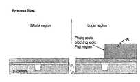
- an initial step and resulting structure, for making an SRAM device structure (in an SRAM region—e.g., FIG. 12 , 13 , 14 or 15 ) connected to a logic device structure (in a Logic region—e.g., FIG. 12 , 13 , 14 or 15 ) according to a preferred inventive embodimentare shown.
- the Logic regionincludes, for example, logic device structures such as “and” gates, “or” gates, or other logic device structures well understood by those skilled in the art.
- a semiconductor substratesuch as a bulk silicon substrate 10 .
- a silicon-on-insulator substrate or Galium Arsenide substratecan be used, alternatively.
- Shallow-trench isolation regionsare formed by conventional techniques, such as by suitable lithography, etching and filling steps.
- STIShallow-trench isolation regions
- a gate oxide 20is grown or deposited.
- a Silicon OxyNitride (SiON) 20is deposited or grown, for example, by conventional techniques, such as by ratio reacting silane, nitric oxide and ammonia at temperatures between 700° C. and 800° C. or in a plasma at temperatures between 200° C. and 350° C.
- the layer 20has a substantially uniform thickness preferably in a range of approximately ( ⁇ 10) 10 ⁇ to 30 ⁇ .
- a polysilicon layer 30is deposited by conventional techniques such as a chemical vapor deposition (CVD) or plasma vapor deposition (PVD) process.
- the layer 30has a substantially uniform thickness preferably in a range of approximately 500 ⁇ to 1200 ⁇ .
- the high-k dielectric material 40is a material having a dielectric constant of greater than seven (7).
- the layer 40has an approximately uniform thickness selected from a range of about 10 ⁇ to about 40 ⁇ .
- High-k materialsare, for example, HfO2, Ta205 or AL2O3.
- the layer 40is deposited by conventional techniques such as CVD or atomic layer deposition (ALD).
- a metal gate material 50is then deposited onto the layer 40 , as shown in FIG. 7 .
- the layer 50has an approximately uniform thickness selected from a range of about 150 ⁇ to about ( ⁇ 10%) 400 ⁇ .
- the material for the layer 50is, for example, TiN, TaN or PtSi.
- the layer 50has a work function selected from a range of approximately 4 eV to approximately 5 eV according to the preferred embodiment of the present invention.
- the layer 50is deposited by conventional techniques such as CVD, sputter deposition or the like.
- FIG. 8cover the SRAM region and a portion of the Logic region with a mask M as shown, using conventional covering or masking techniques well-known. Then, remove portions of the high-k and metal layers 40 , 50 from the PFET Logic region, by conventional techniques such as RIE or CMP (chemical mechanical polishing).
- RIEchemical mechanical polishing
- intermediate gate stacks 40 , 50 , 60 in the SRAM region and the Logic region, and an intermediate gate stack 20 , 60 in the Logic regionby conventional patterning techniques such as reactive ion etch (RIE).
- RIEreactive ion etch
- three of the intermediate gate stacksinclude the layers 40 , 50 , 60 while one of the intermediate gate stacks includes the layers 20 , 60 .
- Spacers 70are then formed by conventional techniques, such as suitable deposition (CVD, PVD or ALD) and etching. See, for example, the patent to Bojarczuk, Jr. et al.
- the spacersare, for example, Si 3 N 4 or SiO 2 . See FIG. 11 .
- Gate caps 80metal silicide are then formed onto the top surfaces of the gate stack as shown.
- the silicide caps 80are formed by conventional techniques (PVD of metal followed with a suitable anneal between 350° C. and 750° C.), and are for example NiSiX, NiPtSiX or CoSi having a substantially uniform thickness in a range of about 100 ⁇ to about 300 ⁇ . As shown, parts of the polysilicon layers 60 are removed to accommodate the caps 80 .
- a final thickness of the layer 40is approximately 20 ⁇
- the layer 50is approximately 150 ⁇
- the layers 60approximately 400 ⁇ and approximately 700 ⁇
- the silicideis approximately 30 ⁇ thick (height).
- NFET and PFET devicesare formed by suitable doping and annealing techniques well known. See, for example, the patent to Bojarczuk, Jr. et al.
- Each of the NFET and PFET deviceshas a respective channel region C, which can be suitably implanted with conventional (1 ⁇ 10 16 ⁇ 1 ⁇ 10 19 atoms/cm 3 ) impurities specific to the respective NFET or PFET device.
- the band gap of the channel region C for the NFETis the same as the band gap of the channel region C of the PFET.
- a liner 90(etch stop) is deposited conventionally, and then an oxide layer 100 deposition is effected.
- the lineris, for example, Si 3 N 4 and has any approximately uniform and suitable thickness.
- the oxide layer 100is SiO 2 , USG, a low-k material or BPSG.
- CMPis performed to planarize the structure. See FIG. 14 .
- electrical contacts 90are formed and connected conventionally to the FETs as shown. See FIG. 15 .
- the contactsare W with Ti/TiN liner, or a Cu contact.
- V min of approximately 0.6 volts to approximately 0.8 volts for the SRAM deviceis achievable.
- the work function of the PFET in the Logic regionis preferably approximately 5.25 eV.
- the band gapis approximately 1.12 volts.
- the difference between the work function of the NFET and the work function of the PFET in the Logic regionis approximately one (1) eV.
Landscapes
- Semiconductor Memories (AREA)
- Metal-Oxide And Bipolar Metal-Oxide Semiconductor Integrated Circuits (AREA)
Abstract
Description
- The present invention relates to CMOS or MOSFET devices and, more particularly, to SRAM (Static Random Access Memory) device structures, semiconductor device structures including SRAM devices, and to methods of manufacture.
- Some prior art CMOS SRAM cells have a six-transistor typology, such as that shown in
FIG. 1 . Others (not shown) have, for example, a four-transistor (4T) topology. 8T topologies are also known. - In
FIG. 1 , two P channel field effect transistors (PFETs) P1,P2 act as pull-up transistors and two N channel field effect transistors (NFETs) N1,N2 act as pull-down transistors. The two NFETs N3,N4 serve as pass gates to control access to the cell for reading and writing to the cell. These pass gates N3,N4 are connected to a word line WL. P1 and N1 form an inverter and P2 and N2 form another inverter. As shown, these inverters are cross-coupled to form a bi-stable cell. - An SRAM array has n rows and m columns of SRAM cells with cells of a row sharing a single word line WL and cells of a column sharing a pair of bit lines BLL and BLR. During standby, all of the word lines WL are low (i.e., at GND) and all bit lines are biased to a voltage level of the power supply Vdd. Thus, the pass-gate transistors of each cell are shut off. A cell state representing a 1 data bit, for example, is established with P1 and N2 on and P2 and N1 off, so that the node L at the left of the cell is high (Vdd) and the node R at the right of the cell is low (GND). A minimum voltage to write or read a state (e.g., 1) to the cell is Vmin. A gate voltage causing formation of an inversion layer at an interface between an insulating layer (oxide) and a substrate (body) of a MOSFET is a threshold voltage Vt. If gate voltage is below the threshold voltage Vtthen the MOSFET is turned off; if the gate voltage is above the threshold voltage Vt, then the MOSFET is turned on.
- As the technology scales, inter-die and intra-die variations in process parameters (e.g., channel length (L), width (W), threshold voltage (Vt), etc.) have become serious problems in circuit design. The device-to-device (intra-die) variations in L, W or Vt between the neighboring transistors in an SRAM cell can significantly degrade not only stability of the cell but also read and write delays. This causes minimum voltage (Vmin) conditions for read and write operations as the PFET threshold voltage degrades because of, for example, the negative bias temperature instability (NBTI) effect after burn-in.
- If the PFET (e.g., P1) is made too strong, then the “write margin” degrades significantly. For example, in the present inventors' opinions, a “super high” Vtin a polysilicon gate would necessitate high dopants that would degrade Vttolerance. To help alleviate these and other problems, the present inventors believe SRAM designs can be directed to compositions and work functions of gate stacks, and to the band gaps, which form various FETs (e.g., P1) of the SRAM cell.
- A work function is a minimum energy (usually measured in electron volts) needed to remove an electron from a solid (e.g., metal) to a point immediately outside the metal. The magnitude of the work function is usually about half of the ionization energy of a free atom of the solid. Also, as is well known, Vtis a function of the following: work function for a gate stack, channel region (under the gate stack) doping and a band gap. For semiconductors, the band gap generally refers to an energy difference between the top of a valence band and the bottom of the conduction band. See, for example, US 2007/0090416 A1, CMOS DEVICES WITH A SINGLE WORK FUNCTION GATE ELECTRODE AND METHOD OF MANUFACTURE, filed Sep. 28, 2005, published Apr. 26, 2007, by Doyle et al.
- According to a preferred embodiment of the present invention, an SRAM device structure includes a first and a second field effect transistor formed on a same semiconductor substrate, each of the transistors including a gate stack, each gate stack including a semiconductor layer disposed on a metal layer, the metal layer being disposed on a high-k dielectric layer located over a channel region, wherein the metal layer of the first gate stack and the metal layer of the second gate stack have approximately a same work function and wherein each channel region has approximately a same band gap.
- It is a principal object of the present invention to provide an SRAM device structure including an SRAM region having an approximately single work function metal and a high-k dielectric disposed in two transistor gate stacks formed on a same semiconductor substrate, and further having approximately equal band gaps in channel regions formed under the gate stacks.
- It is a further object of the present invention to provide an SRAM device structure which has improved low leakage and Vmincharacteristics.
- It is an additional object of the present invention to provide a method of making an SRAM device structure which is compatible with conventional CMOS manufacturing processes.
- It is a still further object of the present invention to provide a method of making an SRAM device structure and a logic device structure on a same semiconductor substrate, the SRAM device structure having an approximately single work function which differs from a work function of the logic device structure.
- Further and still other objects of the present invention will become more readily apparent when the following detailed description is taken in conjunction with the following drawing figures.
FIG. 1 is a schematic circuit diagram of a six transistor (6T) transistor SRAM cell (SRAM device) according to the prior art.FIGS. 2-15 are side-sectional schematic views (not to scale) showing initial, intermediate and final structures during fabrication of an SRAM device structure (in an SRAM region) according to a preferred embodiment of the present invention connected (according to another preferred embodiment) to a logic device structure (fabricated in a Logic region).- Turning now to the figures, it is understood that while the electrical schematic circuit diagram of the preferred embodiments of SRAM device structures according to the present invention is the same as that shown in
FIG. 1 , the physical gate stacks and other structures of the preferred embodiments of the present invention are as shown inFIGS. 9-15 . - As shown beginning in
FIG. 2 , an initial step and resulting structure, for making an SRAM device structure (in an SRAM region—e.g.,FIG. 12 ,13,14 or15) connected to a logic device structure (in a Logic region—e.g.,FIG. 12 ,13,14 or15) according to a preferred inventive embodiment are shown. When completed (e.g.,FIG. 15 ), the Logic region includes, for example, logic device structures such as “and” gates, “or” gates, or other logic device structures well understood by those skilled in the art. - In a first series of steps as explained with reference to
FIG. 2 , provide a semiconductor substrate such as abulk silicon substrate 10. If desired, a silicon-on-insulator substrate or Galium Arsenide substrate can be used, alternatively. Shallow-trench isolation regions (STI) are formed by conventional techniques, such as by suitable lithography, etching and filling steps. For further details, see for example, U.S. Pat. No. 7,105,889 B2, SELECTIVE IMPLEMENTATION OF BARRIER LAYERS TO ACHIEVE THRESHOLD VOLTAGE CONTROL IN CMOS DEVICE FABRICATION WITH HIGH K DIELECTRICS, filed Jun. 4, 2004, issued Sep. 12, 2006, by Bojarczok, Jr. et al., which is hereby incorporated in its entirety by reference. - Next, referring to
FIG. 3 , agate oxide 20 is grown or deposited. A Silicon OxyNitride (SiON)20 is deposited or grown, for example, by conventional techniques, such as by ratio reacting silane, nitric oxide and ammonia at temperatures between 700° C. and 800° C. or in a plasma at temperatures between 200° C. and 350° C. Thelayer 20 has a substantially uniform thickness preferably in a range of approximately (±10) 10 Å to 30 Å. - Referring now to
FIG. 4 , apolysilicon layer 30 is deposited by conventional techniques such as a chemical vapor deposition (CVD) or plasma vapor deposition (PVD) process. Thelayer 30 has a substantially uniform thickness preferably in a range of approximately 500 Å to 1200 Å. - Next, as shown in
FIG. 5 , mask a PFET region of the Logic region with a mask M as shown, by conventional masking techniques (such as with photomask or photo-resist blocking). See also, for example, U.S. Pat. No. 7,112,851, FIELD EFFECT TRANSISTOR WITH ELECTROPLATED METAL GATE, filed Oct. 26, 2005, issued Sep. 26, 2006, by Saenger et al., U.S. Pat. No. 7,279,746 B2, HIGH PERFORMANCE CMOS DEVICE STRUCTURE AND METHOD OF MANUFACTURE, filed Jun. 30, 2003, issued Oct. 9, 2007, by Doris et al., which are all hereby incorporated in their entireties by reference. - As explained with reference to
FIG. 6 , remove the exposed portions of thepolysilicon layer 30 and thegate oxide 20 thereunder by conventional techniques such as reactive ion etching (RIE). Then, remove (strip) the mask M from the remaining intermediate structure conventionally. See, for example, the '851 patent to Saenger et al. - Next, as discussed with reference to
FIG. 7 , deposit a high-k dielectric material, such as a high-k layer orfilm 40, onto the intermediate structure as shown. Preferably, the high-kdielectric material 40 is a material having a dielectric constant of greater than seven (7). Thelayer 40 has an approximately uniform thickness selected from a range of about 10 Å to about 40 Å. High-k materials are, for example, HfO2, Ta205 or AL2O3. Thelayer 40 is deposited by conventional techniques such as CVD or atomic layer deposition (ALD). - A
metal gate material 50 is then deposited onto thelayer 40, as shown inFIG. 7 . - Preferably, the
layer 50 has an approximately uniform thickness selected from a range of about 150 Å to about (±10%) 400 Å. - The material for the
layer 50 is, for example, TiN, TaN or PtSi. Thelayer 50 has a work function selected from a range of approximately 4 eV to approximately 5 eV according to the preferred embodiment of the present invention. Thelayer 50 is deposited by conventional techniques such as CVD, sputter deposition or the like. - Turning now to
FIG. 8 , cover the SRAM region and a portion of the Logic region with a mask M as shown, using conventional covering or masking techniques well-known. Then, remove portions of the high-k andmetal layers - As shown in
FIG. 9 , remove the mask(s) M by conventional methods such as a suitable stripping. - Then, deposit another
polysilicon layer 60 onto the intermediate structure as shown inFIG. 9 . Next, form intermediate gate stacks40,50,60 in the SRAM region and the Logic region, and anintermediate gate stack FIG. 10 , three of the intermediate gate stacks include thelayers layers - Spacers70 (e.g., insulator) are then formed by conventional techniques, such as suitable deposition (CVD, PVD or ALD) and etching. See, for example, the patent to Bojarczuk, Jr. et al. The spacers are, for example, Si3N4or SiO2. See
FIG. 11 . Gate caps80 (metal silicide) are then formed onto the top surfaces of the gate stack as shown. The silicide caps80 are formed by conventional techniques (PVD of metal followed with a suitable anneal between 350° C. and 750° C.), and are for example NiSiX, NiPtSiX or CoSi having a substantially uniform thickness in a range of about 100 Å to about 300 Å. As shown, parts of the polysilicon layers60 are removed to accommodate thecaps 80. - As shown in
FIGS. 12-15 , a final thickness of thelayer 40 is approximately 20 Å, thelayer 50 is approximately 150 Å, thelayers 60 approximately 400 Å and approximately 700 Å, and the silicide is approximately 30 Å thick (height). - Next, appropriate Source and Drain S/D regions are formed for creating NFET and PFET devices by suitable doping and annealing techniques well known. See, for example, the patent to Bojarczuk, Jr. et al. Each of the NFET and PFET devices has a respective channel region C, which can be suitably implanted with conventional (1×10¹⁶−1×10¹⁹atoms/cm3) impurities specific to the respective NFET or PFET device. In the SRAM device, the band gap of the channel region C for the NFET is the same as the band gap of the channel region C of the PFET.
- Finally, a liner90 (etch stop) is deposited conventionally, and then an
oxide layer 100 deposition is effected. The liner is, for example, Si3N4and has any approximately uniform and suitable thickness. Theoxide layer 100 is SiO2, USG, a low-k material or BPSG. Then, CMP is performed to planarize the structure. SeeFIG. 14 . Finally,electrical contacts 90 are formed and connected conventionally to the FETs as shown. SeeFIG. 15 . The contacts are W with Ti/TiN liner, or a Cu contact. - According to the preferred embodiment of the present invention, the inventors believe Vminof approximately 0.6 volts to approximately 0.8 volts for the SRAM device is achievable.
- The work function of the PFET in the Logic region is preferably approximately 5.25 eV. The band gap is approximately 1.12 volts. The difference between the work function of the NFET and the work function of the PFET in the Logic region is approximately one (1) eV.
- Although illustrative embodiments have been described herein with reference to the accompanying drawings, it is to be understood that the present invention is not limited to those precise embodiments, and that various other changes and modifications may be affected therein by one skilled in the art without departing from the scope or spirit of the invention. All such changes and modifications are intended to be included within the scope of the invention as defined by the appended claims. For example, the present invention may be implemented with 4T or even 8T SRAM device structures.
Claims (13)
Priority Applications (1)
| Application Number | Priority Date | Filing Date | Title |
|---|---|---|---|
| US11/968,898US7728392B2 (en) | 2008-01-03 | 2008-01-03 | SRAM device structure including same band gap transistors having gate stacks with high-K dielectrics and same work function |
Applications Claiming Priority (1)
| Application Number | Priority Date | Filing Date | Title |
|---|---|---|---|
| US11/968,898US7728392B2 (en) | 2008-01-03 | 2008-01-03 | SRAM device structure including same band gap transistors having gate stacks with high-K dielectrics and same work function |
Publications (2)
| Publication Number | Publication Date |
|---|---|
| US20090174010A1true US20090174010A1 (en) | 2009-07-09 |
| US7728392B2 US7728392B2 (en) | 2010-06-01 |
Family
ID=40843886
Family Applications (1)
| Application Number | Title | Priority Date | Filing Date |
|---|---|---|---|
| US11/968,898Expired - Fee RelatedUS7728392B2 (en) | 2008-01-03 | 2008-01-03 | SRAM device structure including same band gap transistors having gate stacks with high-K dielectrics and same work function |
Country Status (1)
| Country | Link |
|---|---|
| US (1) | US7728392B2 (en) |
Cited By (2)
| Publication number | Priority date | Publication date | Assignee | Title |
|---|---|---|---|---|
| US20090108373A1 (en)* | 2007-10-30 | 2009-04-30 | International Business Machines Corporation | Techniques for Enabling Multiple Vt Devices Using High-K Metal Gate Stacks |
| CN105097700A (en)* | 2014-04-24 | 2015-11-25 | 中芯国际集成电路制造(上海)有限公司 | Semiconductor device preparation method |
Families Citing this family (2)
| Publication number | Priority date | Publication date | Assignee | Title |
|---|---|---|---|---|
| KR101923946B1 (en) | 2012-08-31 | 2018-11-30 | 삼성전자 주식회사 | Semiconductor device and method for fabricating the same |
| US10170477B2 (en) | 2015-11-06 | 2019-01-01 | International Business Machines Corporation | Forming MOSFET structures with work function modification |
Citations (43)
| Publication number | Priority date | Publication date | Assignee | Title |
|---|---|---|---|---|
| US5265047A (en)* | 1992-03-09 | 1993-11-23 | Monolithic System Technology | High density SRAM circuit with single-ended memory cells |
| US20030104663A1 (en)* | 2001-11-30 | 2003-06-05 | Visokay Mark R. | Multiple work function gates |
| US6734510B2 (en)* | 2001-03-15 | 2004-05-11 | Micron Technology, Ing. | Technique to mitigate short channel effects with vertical gate transistor with different gate materials |
| US6767795B2 (en)* | 2002-01-17 | 2004-07-27 | Micron Technology, Inc. | Highly reliable amorphous high-k gate dielectric ZrOXNY |
| US6806584B2 (en)* | 2002-10-21 | 2004-10-19 | International Business Machines Corporation | Semiconductor device structure including multiple fets having different spacer widths |
| US6809394B1 (en)* | 2003-08-13 | 2004-10-26 | Texas Instruments Incorporated | Dual metal-alloy nitride gate electrodes |
| US6812100B2 (en)* | 2002-03-13 | 2004-11-02 | Micron Technology, Inc. | Evaporation of Y-Si-O films for medium-k dielectrics |
| US6844203B2 (en)* | 2001-08-30 | 2005-01-18 | Micron Technology, Inc. | Gate oxides, and methods of forming |
| US6852167B2 (en)* | 2001-03-01 | 2005-02-08 | Micron Technology, Inc. | Methods, systems, and apparatus for uniform chemical-vapor depositions |
| US6891234B1 (en)* | 2004-01-07 | 2005-05-10 | Acorn Technologies, Inc. | Transistor with workfunction-induced charge layer |
| US6920061B2 (en)* | 2003-08-27 | 2005-07-19 | International Business Machines Corporation | Loadless NMOS four transistor dynamic dual Vt SRAM cell |
| US6924190B2 (en)* | 2000-11-27 | 2005-08-02 | Micron Technology, Inc. | Use of gate electrode workfunction to improve DRAM refresh |
| US6953730B2 (en)* | 2001-12-20 | 2005-10-11 | Micron Technology, Inc. | Low-temperature grown high quality ultra-thin CoTiO3 gate dielectrics |
| US7045430B2 (en)* | 2002-05-02 | 2006-05-16 | Micron Technology Inc. | Atomic layer-deposited LaAlO3 films for gate dielectrics |
| US7049192B2 (en)* | 2003-06-24 | 2006-05-23 | Micron Technology, Inc. | Lanthanide oxide / hafnium oxide dielectrics |
| US7068544B2 (en)* | 2001-08-30 | 2006-06-27 | Micron Technology, Inc. | Flash memory with low tunnel barrier interpoly insulators |
| US7075829B2 (en)* | 2001-08-30 | 2006-07-11 | Micron Technology, Inc. | Programmable memory address and decode circuits with low tunnel barrier interpoly insulators |
| US7105889B2 (en)* | 2004-06-04 | 2006-09-12 | International Business Machines Corporation | Selective implementation of barrier layers to achieve threshold voltage control in CMOS device fabrication with high k dielectrics |
| US7105891B2 (en)* | 2002-07-15 | 2006-09-12 | Texas Instruments Incorporated | Gate structure and method |
| US7105908B2 (en)* | 2003-09-05 | 2006-09-12 | Taiwan Semiconductor Manufacturing Company, Ltd. | SRAM cell having stepped boundary regions and methods of fabrication |
| US7112851B2 (en)* | 2003-10-29 | 2006-09-26 | International Business Machines Corporation | Field effect transistor with electroplated metal gate |
| US7112841B2 (en)* | 2001-08-30 | 2006-09-26 | Micron Technology, Inc. | Graded composition metal oxide tunnel barrier interpoly insulators |
| US7126183B2 (en)* | 2001-08-30 | 2006-10-24 | Micron Technology, Inc. | Programmable array logic or memory with p-channel devices and asymmetrical tunnel barriers |
| US7129580B1 (en)* | 2001-04-17 | 2006-10-31 | Genus, Inc. | Methods and procedures for engineering of composite conductive films by atomic layer deposition |
| US7160577B2 (en)* | 2002-05-02 | 2007-01-09 | Micron Technology, Inc. | Methods for atomic-layer deposition of aluminum oxides in integrated circuits |
| US7164203B1 (en)* | 2001-04-17 | 2007-01-16 | Genus, Inc. | Methods and procedures for engineering of composite conductive by atomic layer deposition |
| US7170809B2 (en)* | 2005-05-13 | 2007-01-30 | International Business Machines Corporation | Stable memory with high mobility cell devices |
| US20070037335A1 (en)* | 2005-08-15 | 2007-02-15 | Texas Instruments Incorporated | Dual work function CMOS devices utilizing carbide based electrodes |
| US20070037333A1 (en)* | 2005-08-15 | 2007-02-15 | Texas Instruments Incorporated | Work function separation for fully silicided gates |
| US7183611B2 (en)* | 2003-06-03 | 2007-02-27 | Micron Technology, Inc. | SRAM constructions, and electronic systems comprising SRAM constructions |
| US20070069302A1 (en)* | 2005-09-28 | 2007-03-29 | Been-Yih Jin | Method of fabricating CMOS devices having a single work function gate electrode by band gap engineering and article made thereby |
| US20070090416A1 (en)* | 2005-09-28 | 2007-04-26 | Doyle Brian S | CMOS devices with a single work function gate electrode and method of fabrication |
| US7217978B2 (en)* | 2005-01-19 | 2007-05-15 | International Business Machines Corporation | SRAM memories and microprocessors having logic portions implemented in high-performance silicon substrates and SRAM array portions having field effect transistors with linked bodies and method for making same |
| US7221017B2 (en)* | 2002-07-08 | 2007-05-22 | Micron Technology, Inc. | Memory utilizing oxide-conductor nanolaminates |
| US7221586B2 (en)* | 2002-07-08 | 2007-05-22 | Micron Technology, Inc. | Memory utilizing oxide nanolaminates |
| US20070178634A1 (en)* | 2006-01-31 | 2007-08-02 | Hyung Suk Jung | Cmos semiconductor devices having dual work function metal gate stacks |
| US7259434B2 (en)* | 2001-08-30 | 2007-08-21 | Micron Technology, Inc. | Highly reliable amorphous high-k gate oxide ZrO2 |
| US7279746B2 (en)* | 2003-06-30 | 2007-10-09 | International Business Machines Corporation | High performance CMOS device structures and method of manufacture |
| US7291527B2 (en)* | 2005-09-07 | 2007-11-06 | Texas Instruments Incorporated | Work function control of metals |
| US7295458B2 (en)* | 2006-01-18 | 2007-11-13 | International Business Machines Corporation | Eight transistor SRAM cell with improved stability requiring only one word line |
| US20080096338A1 (en)* | 2006-10-19 | 2008-04-24 | Texas Instruments Incorporated | Methods and devices employing metal layers in gates to introduce channel strain |
| US20080303060A1 (en)* | 2007-06-06 | 2008-12-11 | Jin-Ping Han | Semiconductor devices and methods of manufacturing thereof |
| US20090108373A1 (en)* | 2007-10-30 | 2009-04-30 | International Business Machines Corporation | Techniques for Enabling Multiple Vt Devices Using High-K Metal Gate Stacks |
- 2008
- 2008-01-03USUS11/968,898patent/US7728392B2/ennot_activeExpired - Fee Related
Patent Citations (52)
| Publication number | Priority date | Publication date | Assignee | Title |
|---|---|---|---|---|
| US5265047A (en)* | 1992-03-09 | 1993-11-23 | Monolithic System Technology | High density SRAM circuit with single-ended memory cells |
| US6924190B2 (en)* | 2000-11-27 | 2005-08-02 | Micron Technology, Inc. | Use of gate electrode workfunction to improve DRAM refresh |
| US6852167B2 (en)* | 2001-03-01 | 2005-02-08 | Micron Technology, Inc. | Methods, systems, and apparatus for uniform chemical-vapor depositions |
| US6734510B2 (en)* | 2001-03-15 | 2004-05-11 | Micron Technology, Ing. | Technique to mitigate short channel effects with vertical gate transistor with different gate materials |
| US7129580B1 (en)* | 2001-04-17 | 2006-10-31 | Genus, Inc. | Methods and procedures for engineering of composite conductive films by atomic layer deposition |
| US7164203B1 (en)* | 2001-04-17 | 2007-01-16 | Genus, Inc. | Methods and procedures for engineering of composite conductive by atomic layer deposition |
| US7183649B1 (en)* | 2001-04-17 | 2007-02-27 | Genus, Inc. | Methods and procedures for engineering of composite conductive films by atomic layer deposition |
| US7259434B2 (en)* | 2001-08-30 | 2007-08-21 | Micron Technology, Inc. | Highly reliable amorphous high-k gate oxide ZrO2 |
| US7068544B2 (en)* | 2001-08-30 | 2006-06-27 | Micron Technology, Inc. | Flash memory with low tunnel barrier interpoly insulators |
| US6844203B2 (en)* | 2001-08-30 | 2005-01-18 | Micron Technology, Inc. | Gate oxides, and methods of forming |
| US7126183B2 (en)* | 2001-08-30 | 2006-10-24 | Micron Technology, Inc. | Programmable array logic or memory with p-channel devices and asymmetrical tunnel barriers |
| US7187587B2 (en)* | 2001-08-30 | 2007-03-06 | Micron Technology, Inc. | Programmable memory address and decode circuits with low tunnel barrier interpoly insulators |
| US7208804B2 (en)* | 2001-08-30 | 2007-04-24 | Micron Technology, Inc. | Crystalline or amorphous medium-K gate oxides, Y203 and Gd203 |
| US7112841B2 (en)* | 2001-08-30 | 2006-09-26 | Micron Technology, Inc. | Graded composition metal oxide tunnel barrier interpoly insulators |
| US7075829B2 (en)* | 2001-08-30 | 2006-07-11 | Micron Technology, Inc. | Programmable memory address and decode circuits with low tunnel barrier interpoly insulators |
| US6770521B2 (en)* | 2001-11-30 | 2004-08-03 | Texas Instruments Incorporated | Method of making multiple work function gates by implanting metals with metallic alloying additives |
| US20030104663A1 (en)* | 2001-11-30 | 2003-06-05 | Visokay Mark R. | Multiple work function gates |
| US6835639B2 (en)* | 2001-11-30 | 2004-12-28 | Texas Instruments Incorporated | Multiple work function gates |
| US6953730B2 (en)* | 2001-12-20 | 2005-10-11 | Micron Technology, Inc. | Low-temperature grown high quality ultra-thin CoTiO3 gate dielectrics |
| US6767795B2 (en)* | 2002-01-17 | 2004-07-27 | Micron Technology, Inc. | Highly reliable amorphous high-k gate dielectric ZrOXNY |
| US7205620B2 (en)* | 2002-01-17 | 2007-04-17 | Micron Technology, Inc. | Highly reliable amorphous high-k gate dielectric ZrOxNy |
| US6930346B2 (en)* | 2002-03-13 | 2005-08-16 | Micron Technology, Inc. | Evaporation of Y-Si-O films for medium-K dielectrics |
| US6812100B2 (en)* | 2002-03-13 | 2004-11-02 | Micron Technology, Inc. | Evaporation of Y-Si-O films for medium-k dielectrics |
| US7160577B2 (en)* | 2002-05-02 | 2007-01-09 | Micron Technology, Inc. | Methods for atomic-layer deposition of aluminum oxides in integrated circuits |
| US7045430B2 (en)* | 2002-05-02 | 2006-05-16 | Micron Technology Inc. | Atomic layer-deposited LaAlO3 films for gate dielectrics |
| US7221586B2 (en)* | 2002-07-08 | 2007-05-22 | Micron Technology, Inc. | Memory utilizing oxide nanolaminates |
| US7221017B2 (en)* | 2002-07-08 | 2007-05-22 | Micron Technology, Inc. | Memory utilizing oxide-conductor nanolaminates |
| US7105891B2 (en)* | 2002-07-15 | 2006-09-12 | Texas Instruments Incorporated | Gate structure and method |
| US6806584B2 (en)* | 2002-10-21 | 2004-10-19 | International Business Machines Corporation | Semiconductor device structure including multiple fets having different spacer widths |
| US7183611B2 (en)* | 2003-06-03 | 2007-02-27 | Micron Technology, Inc. | SRAM constructions, and electronic systems comprising SRAM constructions |
| US7049192B2 (en)* | 2003-06-24 | 2006-05-23 | Micron Technology, Inc. | Lanthanide oxide / hafnium oxide dielectrics |
| US7129553B2 (en)* | 2003-06-24 | 2006-10-31 | Micron Technology, Inc. | Lanthanide oxide/hafnium oxide dielectrics |
| US7279746B2 (en)* | 2003-06-30 | 2007-10-09 | International Business Machines Corporation | High performance CMOS device structures and method of manufacture |
| US6809394B1 (en)* | 2003-08-13 | 2004-10-26 | Texas Instruments Incorporated | Dual metal-alloy nitride gate electrodes |
| US6920061B2 (en)* | 2003-08-27 | 2005-07-19 | International Business Machines Corporation | Loadless NMOS four transistor dynamic dual Vt SRAM cell |
| US7105908B2 (en)* | 2003-09-05 | 2006-09-12 | Taiwan Semiconductor Manufacturing Company, Ltd. | SRAM cell having stepped boundary regions and methods of fabrication |
| US7112851B2 (en)* | 2003-10-29 | 2006-09-26 | International Business Machines Corporation | Field effect transistor with electroplated metal gate |
| US6891234B1 (en)* | 2004-01-07 | 2005-05-10 | Acorn Technologies, Inc. | Transistor with workfunction-induced charge layer |
| US7105889B2 (en)* | 2004-06-04 | 2006-09-12 | International Business Machines Corporation | Selective implementation of barrier layers to achieve threshold voltage control in CMOS device fabrication with high k dielectrics |
| US7217978B2 (en)* | 2005-01-19 | 2007-05-15 | International Business Machines Corporation | SRAM memories and microprocessors having logic portions implemented in high-performance silicon substrates and SRAM array portions having field effect transistors with linked bodies and method for making same |
| US7170809B2 (en)* | 2005-05-13 | 2007-01-30 | International Business Machines Corporation | Stable memory with high mobility cell devices |
| US20070037333A1 (en)* | 2005-08-15 | 2007-02-15 | Texas Instruments Incorporated | Work function separation for fully silicided gates |
| US20070037335A1 (en)* | 2005-08-15 | 2007-02-15 | Texas Instruments Incorporated | Dual work function CMOS devices utilizing carbide based electrodes |
| US7291527B2 (en)* | 2005-09-07 | 2007-11-06 | Texas Instruments Incorporated | Work function control of metals |
| US20070111419A1 (en)* | 2005-09-28 | 2007-05-17 | Doyle Brian S | CMOS Devices with a single work function gate electrode and method of fabrication |
| US20070090416A1 (en)* | 2005-09-28 | 2007-04-26 | Doyle Brian S | CMOS devices with a single work function gate electrode and method of fabrication |
| US20070069302A1 (en)* | 2005-09-28 | 2007-03-29 | Been-Yih Jin | Method of fabricating CMOS devices having a single work function gate electrode by band gap engineering and article made thereby |
| US7295458B2 (en)* | 2006-01-18 | 2007-11-13 | International Business Machines Corporation | Eight transistor SRAM cell with improved stability requiring only one word line |
| US20070178634A1 (en)* | 2006-01-31 | 2007-08-02 | Hyung Suk Jung | Cmos semiconductor devices having dual work function metal gate stacks |
| US20080096338A1 (en)* | 2006-10-19 | 2008-04-24 | Texas Instruments Incorporated | Methods and devices employing metal layers in gates to introduce channel strain |
| US20080303060A1 (en)* | 2007-06-06 | 2008-12-11 | Jin-Ping Han | Semiconductor devices and methods of manufacturing thereof |
| US20090108373A1 (en)* | 2007-10-30 | 2009-04-30 | International Business Machines Corporation | Techniques for Enabling Multiple Vt Devices Using High-K Metal Gate Stacks |
Cited By (6)
| Publication number | Priority date | Publication date | Assignee | Title |
|---|---|---|---|---|
| US20090108373A1 (en)* | 2007-10-30 | 2009-04-30 | International Business Machines Corporation | Techniques for Enabling Multiple Vt Devices Using High-K Metal Gate Stacks |
| US7718496B2 (en)* | 2007-10-30 | 2010-05-18 | International Business Machines Corporation | Techniques for enabling multiple Vt devices using high-K metal gate stacks |
| US20100164011A1 (en)* | 2007-10-30 | 2010-07-01 | International Business Machines Corporation | Techniques for Enabling Multiple Vt Devices Using High-K Metal Gate Stacks |
| US8212322B2 (en)* | 2007-10-30 | 2012-07-03 | International Business Machines Corporation | Techniques for enabling multiple Vt devices using high-K metal gate stacks |
| US8680623B2 (en) | 2007-10-30 | 2014-03-25 | International Business Machines Corporation | Techniques for enabling multiple Vt devices using high-K metal gate stacks |
| CN105097700A (en)* | 2014-04-24 | 2015-11-25 | 中芯国际集成电路制造(上海)有限公司 | Semiconductor device preparation method |
Also Published As
| Publication number | Publication date |
|---|---|
| US7728392B2 (en) | 2010-06-01 |
Similar Documents
| Publication | Publication Date | Title |
|---|---|---|
| US9640540B1 (en) | Structure and method for an SRAM circuit | |
| JP4927321B2 (en) | Semiconductor memory device | |
| US7732872B2 (en) | Integration scheme for multiple metal gate work function structures | |
| US7671422B2 (en) | Pseudo 6T SRAM cell | |
| US6867460B1 (en) | FinFET SRAM cell with chevron FinFET logic | |
| US8129797B2 (en) | Work function engineering for eDRAM MOSFETs | |
| US7915691B2 (en) | High density SRAM cell with hybrid devices | |
| US20160111549A1 (en) | Methods of forming a semiconductor circuit element and semiconductor circuit element | |
| US7550337B2 (en) | Dual gate dielectric SRAM | |
| US20120187504A1 (en) | Semiconductor Device Having Shared Contact Hole and a Manufacturing Method Thereof | |
| US8797787B2 (en) | Semiconductor manufacturing method | |
| JP2589438B2 (en) | Semiconductor memory device and method of manufacturing the same | |
| WO2009123306A1 (en) | Method and device for improving the stability of 6t sgt cmos sram cell | |
| US7728392B2 (en) | SRAM device structure including same band gap transistors having gate stacks with high-K dielectrics and same work function | |
| US7537988B2 (en) | Differential offset spacer | |
| US6847075B2 (en) | Semiconductor integrated circuit apparatus and fabrication method thereof | |
| US7187036B2 (en) | Connection structure for SOI devices | |
| US20090098694A1 (en) | Cd gate bias reduction and differential n+ poly doping for cmos circuits | |
| US9064733B2 (en) | Contact structure for a semiconductor device and methods of making same | |
| WO2023056705A1 (en) | Static random access memory cell and method for forming same | |
| US7588991B2 (en) | Method for fabricating embedded static random access memory | |
| US12433009B2 (en) | Apparatuses including a semiconductor transistor and methods for forming same | |
| US8114729B2 (en) | Differential poly doping and circuits therefrom | |
| TWI433275B (en) | Inverter structure and method for fabricating the same | |
| WO2007063988A1 (en) | Semiconductor device and method for manufacturing same |
Legal Events
| Date | Code | Title | Description |
|---|---|---|---|
| AS | Assignment | Owner name:INTERNATIONAL BUSINESS MACHINES CORPORATION, NEW Y Free format text:ASSIGNMENT OF ASSIGNORS INTEREST;ASSIGNORS:YANG, HAINING S.;WONG, ROBERT C.;REEL/FRAME:020319/0647 Effective date:20071214 Owner name:INTERNATIONAL BUSINESS MACHINES CORPORATION,NEW YO Free format text:ASSIGNMENT OF ASSIGNORS INTEREST;ASSIGNORS:YANG, HAINING S.;WONG, ROBERT C.;REEL/FRAME:020319/0647 Effective date:20071214 | |
| FEPP | Fee payment procedure | Free format text:PAYOR NUMBER ASSIGNED (ORIGINAL EVENT CODE: ASPN); ENTITY STATUS OF PATENT OWNER: LARGE ENTITY | |
| REMI | Maintenance fee reminder mailed | ||
| LAPS | Lapse for failure to pay maintenance fees | ||
| STCH | Information on status: patent discontinuation | Free format text:PATENT EXPIRED DUE TO NONPAYMENT OF MAINTENANCE FEES UNDER 37 CFR 1.362 | |
| FP | Lapsed due to failure to pay maintenance fee | Effective date:20140601 | |
| AS | Assignment | Owner name:GLOBALFOUNDRIES U.S. 2 LLC, NEW YORK Free format text:ASSIGNMENT OF ASSIGNORS INTEREST;ASSIGNOR:INTERNATIONAL BUSINESS MACHINES CORPORATION;REEL/FRAME:036550/0001 Effective date:20150629 | |
| AS | Assignment | Owner name:GLOBALFOUNDRIES INC., CAYMAN ISLANDS Free format text:ASSIGNMENT OF ASSIGNORS INTEREST;ASSIGNORS:GLOBALFOUNDRIES U.S. 2 LLC;GLOBALFOUNDRIES U.S. INC.;REEL/FRAME:036779/0001 Effective date:20150910 |