US20090168486A1 - Large capacity one-time programmable memory cell using metal oxides - Google Patents
Large capacity one-time programmable memory cell using metal oxidesDownload PDFInfo
- Publication number
- US20090168486A1 US20090168486A1US12/005,277US527707AUS2009168486A1US 20090168486 A1US20090168486 A1US 20090168486A1US 527707 AUS527707 AUS 527707AUS 2009168486 A1US2009168486 A1US 2009168486A1
- Authority
- US
- United States
- Prior art keywords
- state
- resistivity
- metal oxide
- forward bias
- diode
- Prior art date
- Legal status (The legal status is an assumption and is not a legal conclusion. Google has not performed a legal analysis and makes no representation as to the accuracy of the status listed.)
- Granted
Links
- 230000015654memoryEffects0.000titleclaimsabstractdescription77
- 229910044991metal oxideInorganic materials0.000titleclaimsabstractdescription47
- 150000004706metal oxidesChemical class0.000titleclaimsabstractdescription47
- 238000000034methodMethods0.000claimsabstractdescription23
- 229910021420polycrystalline siliconInorganic materials0.000claimsdescription11
- 229920005591polysiliconPolymers0.000claimsdescription10
- GWEVSGVZZGPLCZ-UHFFFAOYSA-NTitan oxideChemical compoundO=[Ti]=OGWEVSGVZZGPLCZ-UHFFFAOYSA-N0.000claimsdescription6
- MCMNRKCIXSYSNV-UHFFFAOYSA-NZirconium dioxideChemical compoundO=[Zr]=OMCMNRKCIXSYSNV-UHFFFAOYSA-N0.000claimsdescription6
- AYTAKQFHWFYBMA-UHFFFAOYSA-Nchromium dioxideChemical compoundO=[Cr]=OAYTAKQFHWFYBMA-UHFFFAOYSA-N0.000claimsdescription6
- ZKATWMILCYLAPD-UHFFFAOYSA-Nniobium pentoxideChemical compoundO=[Nb](=O)O[Nb](=O)=OZKATWMILCYLAPD-UHFFFAOYSA-N0.000claimsdescription6
- PNEYBMLMFCGWSK-UHFFFAOYSA-Naluminium oxideInorganic materials[O-2].[O-2].[O-2].[Al+3].[Al+3]PNEYBMLMFCGWSK-UHFFFAOYSA-N0.000claimsdescription3
- 229910052593corundumInorganic materials0.000claimsdescription3
- CJNBYAVZURUTKZ-UHFFFAOYSA-Nhafnium(IV) oxideInorganic materialsO=[Hf]=OCJNBYAVZURUTKZ-UHFFFAOYSA-N0.000claimsdescription3
- CPLXHLVBOLITMK-UHFFFAOYSA-Nmagnesium oxideInorganic materials[Mg]=OCPLXHLVBOLITMK-UHFFFAOYSA-N0.000claimsdescription3
- GNRSAWUEBMWBQH-UHFFFAOYSA-Nnickel(II) oxideInorganic materials[Ni]=OGNRSAWUEBMWBQH-UHFFFAOYSA-N0.000claimsdescription3
- PBCFLUZVCVVTBY-UHFFFAOYSA-Ntantalum pentoxideInorganic materialsO=[Ta](=O)O[Ta](=O)=OPBCFLUZVCVVTBY-UHFFFAOYSA-N0.000claimsdescription3
- 229910001845yogo sapphireInorganic materials0.000claimsdescription3
- 229910002938(Ba,Sr)TiO3Inorganic materials0.000claimsdescription2
- 229910002971CaTiO3Inorganic materials0.000claimsdescription2
- 239000004065semiconductorSubstances0.000description12
- 239000004020conductorSubstances0.000description11
- 239000000463materialSubstances0.000description10
- 239000000758substrateSubstances0.000description8
- 229910021332silicideInorganic materials0.000description7
- XUIMIQQOPSSXEZ-UHFFFAOYSA-NSiliconChemical compound[Si]XUIMIQQOPSSXEZ-UHFFFAOYSA-N0.000description6
- 229910052710siliconInorganic materials0.000description6
- 239000010703siliconSubstances0.000description6
- 230000007704transitionEffects0.000description6
- 239000002019doping agentSubstances0.000description5
- FVBUAEGBCNSCDD-UHFFFAOYSA-Nsilicide(4-)Chemical compound[Si-4]FVBUAEGBCNSCDD-UHFFFAOYSA-N0.000description5
- 238000003491arrayMethods0.000description3
- 230000007547defectEffects0.000description3
- 230000008021depositionEffects0.000description3
- VYPSYNLAJGMNEJ-UHFFFAOYSA-NSilicium dioxideChemical compoundO=[Si]=OVYPSYNLAJGMNEJ-UHFFFAOYSA-N0.000description2
- 229910000577Silicon-germaniumInorganic materials0.000description2
- LEVVHYCKPQWKOP-UHFFFAOYSA-N[Si].[Ge]Chemical compound[Si].[Ge]LEVVHYCKPQWKOP-UHFFFAOYSA-N0.000description2
- 229910045601alloyInorganic materials0.000description2
- 239000000956alloySubstances0.000description2
- 229910021417amorphous siliconInorganic materials0.000description2
- QVGXLLKOCUKJST-UHFFFAOYSA-Natomic oxygenChemical compound[O]QVGXLLKOCUKJST-UHFFFAOYSA-N0.000description2
- 150000004770chalcogenidesChemical class0.000description2
- 239000013078crystalSubstances0.000description2
- 238000002425crystallisationMethods0.000description2
- 230000008025crystallizationEffects0.000description2
- 238000010586diagramMethods0.000description2
- 229910052732germaniumInorganic materials0.000description2
- GNPVGFCGXDBREM-UHFFFAOYSA-Ngermanium atomChemical compound[Ge]GNPVGFCGXDBREM-UHFFFAOYSA-N0.000description2
- 238000004519manufacturing processMethods0.000description2
- 229910021424microcrystalline siliconInorganic materials0.000description2
- 229910052760oxygenInorganic materials0.000description2
- 239000001301oxygenSubstances0.000description2
- ATJFFYVFTNAWJD-UHFFFAOYSA-NTinChemical compound[Sn]ATJFFYVFTNAWJD-UHFFFAOYSA-N0.000description1
- NRTOMJZYCJJWKI-UHFFFAOYSA-NTitanium nitrideChemical compound[Ti]#NNRTOMJZYCJJWKI-UHFFFAOYSA-N0.000description1
- 230000004888barrier functionEffects0.000description1
- 238000012512characterization methodMethods0.000description1
- 239000010941cobaltSubstances0.000description1
- 229910017052cobaltInorganic materials0.000description1
- GUTLYIVDDKVIGB-UHFFFAOYSA-Ncobalt atomChemical compound[Co]GUTLYIVDDKVIGB-UHFFFAOYSA-N0.000description1
- 238000010276constructionMethods0.000description1
- 238000011109contaminationMethods0.000description1
- 230000000694effectsEffects0.000description1
- 238000002955isolationMethods0.000description1
- 229910052751metalInorganic materials0.000description1
- 239000002184metalSubstances0.000description1
- 230000007935neutral effectEffects0.000description1
- 239000000377silicon dioxideSubstances0.000description1
- 235000012239silicon dioxideNutrition0.000description1
- 239000002210silicon-based materialSubstances0.000description1
- 229910021341titanium silicideInorganic materials0.000description1
- WFKWXMTUELFFGS-UHFFFAOYSA-NtungstenChemical compound[W]WFKWXMTUELFFGS-UHFFFAOYSA-N0.000description1
- 239000010937tungstenSubstances0.000description1
- 229910052721tungstenInorganic materials0.000description1
Images


Classifications
- G—PHYSICS
- G11—INFORMATION STORAGE
- G11C—STATIC STORES
- G11C11/00—Digital stores characterised by the use of particular electric or magnetic storage elements; Storage elements therefor
- G11C11/56—Digital stores characterised by the use of particular electric or magnetic storage elements; Storage elements therefor using storage elements with more than two stable states represented by steps, e.g. of voltage, current, phase, frequency
- G11C11/5685—Digital stores characterised by the use of particular electric or magnetic storage elements; Storage elements therefor using storage elements with more than two stable states represented by steps, e.g. of voltage, current, phase, frequency using storage elements comprising metal oxide memory material, e.g. perovskites
- G—PHYSICS
- G11—INFORMATION STORAGE
- G11C—STATIC STORES
- G11C11/00—Digital stores characterised by the use of particular electric or magnetic storage elements; Storage elements therefor
- G11C11/56—Digital stores characterised by the use of particular electric or magnetic storage elements; Storage elements therefor using storage elements with more than two stable states represented by steps, e.g. of voltage, current, phase, frequency
- G11C11/5692—Digital stores characterised by the use of particular electric or magnetic storage elements; Storage elements therefor using storage elements with more than two stable states represented by steps, e.g. of voltage, current, phase, frequency read-only digital stores using storage elements with more than two stable states
- G—PHYSICS
- G11—INFORMATION STORAGE
- G11C—STATIC STORES
- G11C13/00—Digital stores characterised by the use of storage elements not covered by groups G11C11/00, G11C23/00, or G11C25/00
- G11C13/0002—Digital stores characterised by the use of storage elements not covered by groups G11C11/00, G11C23/00, or G11C25/00 using resistive RAM [RRAM] elements
- G11C13/0007—Digital stores characterised by the use of storage elements not covered by groups G11C11/00, G11C23/00, or G11C25/00 using resistive RAM [RRAM] elements comprising metal oxide memory material, e.g. perovskites
- G—PHYSICS
- G11—INFORMATION STORAGE
- G11C—STATIC STORES
- G11C13/00—Digital stores characterised by the use of storage elements not covered by groups G11C11/00, G11C23/00, or G11C25/00
- G11C13/0002—Digital stores characterised by the use of storage elements not covered by groups G11C11/00, G11C23/00, or G11C25/00 using resistive RAM [RRAM] elements
- G11C13/0021—Auxiliary circuits
- G11C13/0069—Writing or programming circuits or methods
- G—PHYSICS
- G11—INFORMATION STORAGE
- G11C—STATIC STORES
- G11C17/00—Read-only memories programmable only once; Semi-permanent stores, e.g. manually-replaceable information cards
- G11C17/14—Read-only memories programmable only once; Semi-permanent stores, e.g. manually-replaceable information cards in which contents are determined by selectively establishing, breaking or modifying connecting links by permanently altering the state of coupling elements, e.g. PROM
- G11C17/16—Read-only memories programmable only once; Semi-permanent stores, e.g. manually-replaceable information cards in which contents are determined by selectively establishing, breaking or modifying connecting links by permanently altering the state of coupling elements, e.g. PROM using electrically-fusible links
- G11C17/165—Memory cells which are electrically programmed to cause a change in resistance, e.g. to permit multiple resistance steps to be programmed rather than conduct to or from non-conduct change of fuses and antifuses
- G—PHYSICS
- G11—INFORMATION STORAGE
- G11C—STATIC STORES
- G11C13/00—Digital stores characterised by the use of storage elements not covered by groups G11C11/00, G11C23/00, or G11C25/00
- G11C13/0002—Digital stores characterised by the use of storage elements not covered by groups G11C11/00, G11C23/00, or G11C25/00 using resistive RAM [RRAM] elements
- G11C13/0021—Auxiliary circuits
- G11C13/0069—Writing or programming circuits or methods
- G11C2013/0078—Write using current through the cell
- G—PHYSICS
- G11—INFORMATION STORAGE
- G11C—STATIC STORES
- G11C13/00—Digital stores characterised by the use of storage elements not covered by groups G11C11/00, G11C23/00, or G11C25/00
- G11C13/0002—Digital stores characterised by the use of storage elements not covered by groups G11C11/00, G11C23/00, or G11C25/00 using resistive RAM [RRAM] elements
- G11C13/0021—Auxiliary circuits
- G11C13/0069—Writing or programming circuits or methods
- G11C2013/009—Write using potential difference applied between cell electrodes
- G—PHYSICS
- G11—INFORMATION STORAGE
- G11C—STATIC STORES
- G11C2213/00—Indexing scheme relating to G11C13/00 for features not covered by this group
- G11C2213/30—Resistive cell, memory material aspects
- G11C2213/31—Material having complex metal oxide, e.g. perovskite structure
- G—PHYSICS
- G11—INFORMATION STORAGE
- G11C—STATIC STORES
- G11C2213/00—Indexing scheme relating to G11C13/00 for features not covered by this group
- G11C2213/30—Resistive cell, memory material aspects
- G11C2213/32—Material having simple binary metal oxide structure
- G—PHYSICS
- G11—INFORMATION STORAGE
- G11C—STATIC STORES
- G11C2213/00—Indexing scheme relating to G11C13/00 for features not covered by this group
- G11C2213/70—Resistive array aspects
- G11C2213/71—Three dimensional array
- G—PHYSICS
- G11—INFORMATION STORAGE
- G11C—STATIC STORES
- G11C2213/00—Indexing scheme relating to G11C13/00 for features not covered by this group
- G11C2213/70—Resistive array aspects
- G11C2213/72—Array wherein the access device being a diode
Definitions
- the inventionrelates to a nonvolatile memory array.
- Nonvolatile memory arraysmaintain their data even when power to the device is turned off.
- each memory cellis formed in an initial unprogrammed state, and can be converted to a programmed state. This change is permanent, and such cells are not erasable. In other types of memories, the memory cells are erasable, and can be rewritten many times.
- Cellsmay also vary in the number of data states each cell can achieve.
- a data statemay be stored by altering some characteristic of the cell which can be detected, such as current flowing through the cell under a given applied voltage or the threshold voltage of a transistor within the cell.
- a data stateis a distinct value of the cell, such as a data ‘0’ or a data ‘1’.
- Floating gate and SONOS memory cellsoperate by storing charge, where the presence, absence or amount of stored charge changes a transistor threshold voltage. These memory cells are three-terminal devices that are relatively difficult to fabricate and operate at the very small dimensions required for competitiveness in modern integrated circuits.
- Chalcogenidesare difficult to work with and can present challenges in most semiconductor production facilities.
- nonvolatile memory arrayhaving erasable or multi-state memory cells formed using semiconductor materials in structures that are readily scaled to small size and having a capacity of more than 1 bit/cell (i.e., ⁇ 2 bits/cell) is desirable.
- On embodiment of the inventionprovides a method of programming a nonvolatile memory device, comprising (i) providing a nonvolatile memory cell comprising a diode in series with at least one metal oxide, (ii) applying a first forward bias to change a resistivity state of the metal oxide from a first state to a second state; (iii) applying a second forward bias to change a resistivity state of the metal oxide from a second state to a third state; and (iv) applying a third forward bias to change a resistivity state of the metal oxide from a third state to a fourth state.
- the fourth resistivity stateis higher than the third resistivity state, the third resistivity state is lower than the second resistivity state, and the second resistivity state is lower than the first resistivity state.
- FIG. 1is a circuit diagram illustrating the need for electrical isolation between memory cells in a memory array.
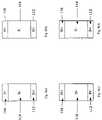
- FIG. 2is a perspective view of a memory cell formed according to a preferred embodiment of the present invention.
- FIGS. 3( a )- 3 ( b )are side cross-sectional views illustrating two embodiments of a memory cell.
- FIGS. 4( a )- 4 ( d )are schematic side cross-sectional views illustrating alternative diode configurations according to an embodiment of the present invention.
- FIG. 5is a circuit diagram showing a biasing scheme to bias the cell in forward bias.
- FIG. 6is a probability plot showing memory cells transformed from the first state 1 to the second state 2 , from the second state 2 to the third state 3 , and from the third state 3 to the fourth state 4 .
- trimmable resistorshave been used as elements in integrated circuits.
- resistorsare used as memory cells in a large cross-point array, when voltage is applied to a selected cell, there will be undesired leakage through half-selected and unselected cells throughout the array. For example, turning to FIG. 1 , suppose a voltage is applied between bitline B and wordline A to set, reset, or sense selected cell S. Current is intended to flow through selected cell S. Some leakage current, however, may flow on alternate paths, for example between bitline B and wordline A through unselected cells U 1 , U 2 , and U 3 . Many such alternate paths may exist.
- Leakage currentcan be greatly reduced by forming each memory with a diode.
- a diodehas a non-linear I-V characteristic, allowing very little current flow below a turn-on voltage, and substantially higher current flow above the turn-on voltage.
- a diodealso acts as one-way valves passing current more easily in one direction than the other.
- transition from a higher- to a lower-resistivity statewill be called a set transition, affected by a set current, a set or programming voltage, or a set or programming pulse; while the reverse transition, from a lower- to a higher-resistivity state, will be called a reset transition, affected by a reset current, a reset voltage, or a reset pulse which places the diode in an unprogrammed state.
- the memory cellincludes a cylindrical semiconductor diode is located in series with a cylindrical metal oxide layer or film.
- the diode and the filmare disposed between two electrodes, as illustrated in FIG. 2 .
- the number of oxide layers or filmsneed not be limited to one; for example, it can be two or more.
- the diode and metal oxide filmmay have a shape other than cylindrical, if desired.
- the metal oxide filmserves as the resistivity switching element and the diode as the steering element of the memory cell.
- FIG. 2illustrates the perspective view of a memory cell formed according to a preferred embodiment of the present invention.
- a bottom conductor 101is formed of a conductive material, for example tungsten, and extends in a first direction. Barrier and adhesion layers, such as TiN layers, may be included in bottom conductor 101 .
- the semiconductor diode 110has a bottom heavily doped n-type region 112 ; an intrinsic region 114 , which is not intentionally doped; and a top heavily doped p-type region 116 , though the orientation of this diode may be reversed, as shown in FIGS. 4 a to 4 d. Such a diode, regardless of its orientation, will be referred to as a p-i-n diode or simply diode.
- a metal oxide layer 118is disposed on the diode, either on the p-type region 116 or below the n-region 112 of the diode 110 , as shown for example in FIGS. 3( a ) and 3 ( b ).
- Top conductor 100may be formed in the same manner and of the same materials as bottom conductor 101 , and extends in a second direction different from the first direction.
- the semiconductor diode 110is vertically disposed between bottom conductor 101 and top conductor 100 .
- the diodecan comprise any single crystal, polycrystalline, or amorphous semiconductor material, such as silicon, germanium, or silicon-germanium alloys.
- the diode 110comprise three different regions 112 , 114 , 116 .
- a region of semiconductor material which is not intentionally dopedis described as an intrinsic region 114 as shown in FIG. 2 and FIGS. 3( a )-( b ).
- an intrinsic regionmay in fact include a low concentration of p-type or n-type dopants. Dopants may diffuse into the intrinsic region from the adjacent n or p-doped regions ( 112 and 116 , respectively in FIGS. 3( a ) and 3 ( b )) or may be present in the deposition chamber during deposition due to contamination from an earlier deposition.
- deposited intrinsic semiconductor materialmay include defects which cause it to behave as if slightly n-doped.
- intrinsic semiconductorto describe silicon, germanium, a silicon-germanium alloy, or some other semiconductor material is not meant to imply that this region contains no dopants whatsoever, nor that such a region is perfectly electrically neutral.
- the diodeneed not be limited to a p-i-n design as described; rather, a diode can comprise a combination of the different regions, each with different concentrations of dopants, as illustrated in FIGS. 4( a )- 4 ( d ).
- amorphous or microcrystalline siliconWhen amorphous or microcrystalline silicon is crystallized in contact with one of these silicides, the crystal lattice of the silicide provides a template to the silicon during crystallization.
- the resulting polysiliconwill be highly ordered, and relatively low in defects.
- This high-quality polysiliconwhen doped with a conductivity-enhancing dopant, is relatively highly conductive as formed.
- Such a diodepreferably acts as a steering element of the memory cell because the diode does not change resistivity when certain voltage pulses are applied which are sufficient to switch the resistivity state of the metal oxide film.
- amorphous or microcrystalline silicon materialwhen crystallized not in contact with a silicide with which it has a good lattice match, for example when silicon is crystallized in contact only with materials such as silicon dioxide and titanium nitride, with which it has a significant lattice mismatch, the resulting polysilicon will have many more defects, and doped polysilicon crystallized this way will be much less conductive as formed.
- Such diodecan switch resistivity state when bias is applied.
- the diodecan also serve as a resistivity switching element and as the steering element of the memory cell.
- the metal oxide filmcan be any resistivity switching metal oxide film, such as a pervoskite, such as CaTiO 3 or (Ba,Sr)TiO 3 , or NiO, Nb 2 O 5 , TiO 2 , HfO 2 , Al 2 O 3 , MgO, CrO 2 , ZnO 2 , ZrO 2 , VO, or Ta 2 O 5 .
- the thickness of the metal oxide in the preferred embodiments of the inventioncan be preferably about 20-1000 ⁇ , more preferably about 40-400 ⁇ , or more preferably about 70-100 ⁇ .
- the memory cellinitially starts in a high resistivity, low read current state (referred to as the unprogrammed or virgin state).
- the cellcan be put in the programmed, low resistivity state by a high forward bias voltage pulse, preferably at the factory where the cell is made before the product is sold, where power is not a consideration.
- the cellis subsequently put in one or more other states by subsequent forward bias programming pulses.
- the difference between the read currents of the unprogrammed and programmed statesconstitutes the “window” for the memory cell. It is desirable for this window to be as large as possible for manufacturing robustness.
- the present inventorsrealized that the read current window of the programmed cell and the number of bits per cell can be increased by the following programming method.
- the resistivity of the metal oxidecan be changed between stable states by applying appropriate electrical pulses.
- the set and reset transitionsare performed with metal oxide under forward bias.
- More than one programming pulsecan be used. For example, a plurality of forward bias pulses are applied to the cell to switch the metal oxide from a high resistivity, unprogrammed state to a low resistivity, programmed state.
- the conductivity, or inversely the resistivity, of the metal oxidecan be modified because the conductivity of the oxide is largely affected by the movements of the oxygen vacancies.
- a partial depletion of the oxygen vacancies as a result of the vacancies moving out of the oxide film surfacecan result in an increase of the conductivity, or conversely, a decrease in resistivity.
- Distinct data states of the memory cell of the embodiments of the present inventionthus correspond to resistivity states of the metal oxide in series with the diode.
- the memory cellcan be put into distinct data states by a series of distinct forward biases, preferably ranging from 1 to 20 V, more preferably from 2 to 10 V, and more preferably from 3 to 8 V.
- the current flowing through the cell between any one distinct data state and any different distinct data stateis different by at least a factor of two, to allow the difference between the states to be readily detectable.
- a diode formed of polycrystalline semiconductor material and at least one metal oxideare arranged in series.
- the deviceis used as a one-time programmable multilevel cell, in preferred embodiments having four distinct data states.
- one-time programmablemeans that cell can be non-reversibly programmed into up to four different states.
- a forward biasis applied to the cell having a magnitude greater than a minimum voltage required for programming the cell.
- FIG. 5illustrates the application of a forward bias to a portion of a memory cell array. For example, if the minimum voltage required to program the cell is 4 V, then a programming forward bias of 5 or more volts, such as about 8 V to about 12 V, for example 10 V, is applied to the selected cells. The forward bias switches the cell from a relatively high resistivity, unprogrammed state to a relatively low resistivity, programmed state. If desired, the maximum voltage which can be applied without damaging the diode may be used as the programming voltage.
- FIG. 6is a probability plot showing read current of a memory cell at 2 V in various states.
- a series of 3 forward biasesare applied.
- a first forward bias current limited voltage (V 1 ⁇ 2 )(i.e., the programming pulse described above) lowers the resistivity of the metal oxide and changes the resistivity state of the cell from the first state 1 to the second state 2 .
- a second higher current limited forward bias voltage (V 2 ⁇ 3 )further lowers the resistivity of the oxide and changes the resistivity state of the cell from the second state 2 to the third state 3 .
- a third even higher current limited forward bias voltageincreases the resistivity of the metal oxide and changes the resistivity state of the cell from the third state 3 to the fourth state 4 .
- state 2is obtained with a predetermined voltage at a predetermined current limit.
- state 3is obtained with a higher voltage and at a higher current limit than state 2 .
- state 4is obtained with a lower voltage than state 3 , but at a higher current limit than state 3 (i.e., the current limit to obtain state 4 is the highest current limit of the four states).
- the successive current limits for the different statesensure that state 2 is obtained without moving directly to state 3 or 4 without going through state 2 by the application of the forward bias voltages.
- the four resistivity states of the oxideare distinguishable from the states of the diode, which in the preferred embodiments is used as a steering element and has minimal effects on change of cell resistivity.
- the initial read currentis between about 1 ⁇ 10 ⁇ 13 and 2 ⁇ 10 ⁇ 13 A when a first electrical forward bias pulse, V 1 ⁇ 2 , is applied.
- the pulsehas a magnitude greater than a minimum voltage required for programming the cell.
- the voltage appliedcan be about 10 V.
- the pulse widthcan be between about 100 and about 500 nsec.
- This first electrical pulseswitches the metal oxide from a first resistivity state 1 to a second resistivity state 2 , with the second state having lower resistivity than the first state; this transition is labeled “1 ⁇ 2” in FIG. 6 .
- the resultant read current in the F stateis between about 2 ⁇ 10 ⁇ 6 and 11 ⁇ 10 ⁇ 6 A.
- a second forward bias pulse V 2 ⁇ 3is then applied, with V 2 ⁇ 3 being larger than V 1 ⁇ 2 , further lowering the resistivity of the oxide.
- the resulting read current of the cellis between about 2 ⁇ 10 ⁇ 5 and 10 ⁇ 10 ⁇ 5 A.
- a third forward bias pulse V 3 ⁇ 4is applied, with V 3 ⁇ 4 being smaller than V 2 ⁇ 3 , increasing the resistivity of the oxide.
- the resulting read currentis between about 0.7 ⁇ 10 ⁇ 7 and 4 ⁇ 10 ⁇ 7 A.
- a device for programming the memory cellsis a driver circuit located under, over, or adjacent to the memory cell.
- the circuitcan have a monolithic integrated structure, or a plurality of integrated device packaged together or in close proximity or die-bonded together.
- the driver circuitsee for example, U.S. patent application Ser. No. 10/185,508 by Cleeves; U.S. patent application Ser. No. 09/560,626 by Knall; and U.S. Pat. No. 6,055,180 to Gudensen et al., each of which is hereby incorporated by reference.
- the memory cellis preferably a one-time programmable cell, but it can also be used as a rewriteable memory cell, and may have two, three, four, or more distinct data states.
- the resistivity of the metal oxideis higher than that of the diode.
- the memory cellmay be fabricated by any suitable methods.
- the methods described U.S. patent application Ser. No. 11/125,939 filed on May 9, 2005which corresponds to US Published Application No. 2006/0250836 to Herner et al.
- U.S. patent application Ser. No. 11/395,995 filed on Mar. 31, 2006which corresponds to US Patent Published Application No. 2006/0250837 to Herner et al., which are incorporated by reference in their entirety may be used.
- the above described memory cell shown in FIG. 2may be located in a one memory level device. If desired, additional memory levels can be formed above the first memory level to form a monolithic three dimensional memory array. In some embodiments, conductors can be shared between memory levels; i.e. top conductor 100 shown in FIG. 2 would serve as the bottom conductor of the next memory level. In other embodiments, an interlevel dielectric (not shown) is formed above the first memory level, its surface planarized, and construction of a second memory level begins on this planarized interlevel dielectric, with no shared conductors.
- a monolithic three dimensional memory arrayis one in which multiple memory levels are formed above a single substrate, such as a wafer, with no intervening substrates.
- the layers forming one memory levelare deposited or grown directly over the layers of an existing level or levels.
- stacked memorieshave been constructed by forming memory levels on separate substrates and adhering the memory levels atop each other, as in Leedy, U.S. Pat. No. 5,915,167, “Three dimensional structure memory.”
- the substratesmay be thinned or removed from the memory levels before bonding, but as the memory levels are initially formed over separate substrates, such memories are not true monolithic three dimensional memory arrays.
- a monolithic three dimensional memory array formed above a substratecomprises at least a first memory level formed at a first height above the substrate and a second memory level formed at a second height different from the first height. Three, four, eight, or indeed any number of memory levels can be formed above the substrate in such a multilevel array.
Landscapes
- Engineering & Computer Science (AREA)
- Chemical & Material Sciences (AREA)
- Materials Engineering (AREA)
- Computer Hardware Design (AREA)
- Semiconductor Memories (AREA)
Abstract
Description
- The invention relates to a nonvolatile memory array.
- Nonvolatile memory arrays maintain their data even when power to the device is turned off. In one-time programmable arrays, each memory cell is formed in an initial unprogrammed state, and can be converted to a programmed state. This change is permanent, and such cells are not erasable. In other types of memories, the memory cells are erasable, and can be rewritten many times.
- Cells may also vary in the number of data states each cell can achieve. A data state may be stored by altering some characteristic of the cell which can be detected, such as current flowing through the cell under a given applied voltage or the threshold voltage of a transistor within the cell. A data state is a distinct value of the cell, such as a data ‘0’ or a data ‘1’.
- Some solutions for achieving erasable or multi-state cells are complex. Floating gate and SONOS memory cells, for example, operate by storing charge, where the presence, absence or amount of stored charge changes a transistor threshold voltage. These memory cells are three-terminal devices that are relatively difficult to fabricate and operate at the very small dimensions required for competitiveness in modern integrated circuits.
- Other memory cells operate by changing the resistivity of relatively exotic materials, like chalcogenides. Chalcogenides are difficult to work with and can present challenges in most semiconductor production facilities.
- Thus, a nonvolatile memory array having erasable or multi-state memory cells formed using semiconductor materials in structures that are readily scaled to small size and having a capacity of more than 1 bit/cell (i.e., ≧2 bits/cell) is desirable.
- On embodiment of the invention provides a method of programming a nonvolatile memory device, comprising (i) providing a nonvolatile memory cell comprising a diode in series with at least one metal oxide, (ii) applying a first forward bias to change a resistivity state of the metal oxide from a first state to a second state; (iii) applying a second forward bias to change a resistivity state of the metal oxide from a second state to a third state; and (iv) applying a third forward bias to change a resistivity state of the metal oxide from a third state to a fourth state. The fourth resistivity state is higher than the third resistivity state, the third resistivity state is lower than the second resistivity state, and the second resistivity state is lower than the first resistivity state.
FIG. 1 is a circuit diagram illustrating the need for electrical isolation between memory cells in a memory array.FIG. 2 is a perspective view of a memory cell formed according to a preferred embodiment of the present invention.FIGS. 3( a)-3(b) are side cross-sectional views illustrating two embodiments of a memory cell.FIGS. 4( a)-4(d) are schematic side cross-sectional views illustrating alternative diode configurations according to an embodiment of the present invention.FIG. 5 is a circuit diagram showing a biasing scheme to bias the cell in forward bias.FIG. 6 is a probability plot showing memory cells transformed from thefirst state 1 to thesecond state 2, from thesecond state 2 to thethird state 3, and from thethird state 3 to thefourth state 4.- It has been known that by applying electrical pulses, the resistance of a resistor formed of doped polycrystalline silicon, or polysilicon, can be trimmed, adjusting it between stable resistance states. Such trimmable resistors have been used as elements in integrated circuits.
- However, making a memory array of polysilicon resistors presents difficulties. If resistors are used as memory cells in a large cross-point array, when voltage is applied to a selected cell, there will be undesired leakage through half-selected and unselected cells throughout the array. For example, turning to
FIG. 1 , suppose a voltage is applied between bitline B and wordline A to set, reset, or sense selected cell S. Current is intended to flow through selected cell S. Some leakage current, however, may flow on alternate paths, for example between bitline B and wordline A through unselected cells U1, U2, and U3. Many such alternate paths may exist. - Leakage current can be greatly reduced by forming each memory with a diode. A diode has a non-linear I-V characteristic, allowing very little current flow below a turn-on voltage, and substantially higher current flow above the turn-on voltage. In general a diode also acts as one-way valves passing current more easily in one direction than the other. Thus, so long as biasing schemes are selected that assure that only the selected cell is subjected to a forward current above the turn-on voltage, leakage current along unintended paths (such as the U1-U2-U3 sneak path of
FIG. 1 ) can be greatly reduced. - In this discussion, transition from a higher- to a lower-resistivity state will be called a set transition, affected by a set current, a set or programming voltage, or a set or programming pulse; while the reverse transition, from a lower- to a higher-resistivity state, will be called a reset transition, affected by a reset current, a reset voltage, or a reset pulse which places the diode in an unprogrammed state.
- In preferred embodiments, the memory cell includes a cylindrical semiconductor diode is located in series with a cylindrical metal oxide layer or film. The diode and the film are disposed between two electrodes, as illustrated in
FIG. 2 . The number of oxide layers or films need not be limited to one; for example, it can be two or more. The diode and metal oxide film may have a shape other than cylindrical, if desired. For a detailed description of a the design of a memory cell comprising a diode and a metal oxide, see for example U.S. patent application Ser. No. 11/125,939 filed on May 9, 2005 (which corresponds to US Published Application No. 2006/0250836 to Herner et al.), and U.S. patent application Ser. No. 11/395,995 filed on Mar. 31, 2006 (which corresponds to US Patent Published Application No. 2006/0250837 to Herner et al.,) each of which is hereby incorporated by reference. In the preferred embodiments of the invention, the metal oxide film serves as the resistivity switching element and the diode as the steering element of the memory cell. FIG. 2 illustrates the perspective view of a memory cell formed according to a preferred embodiment of the present invention. Abottom conductor 101 is formed of a conductive material, for example tungsten, and extends in a first direction. Barrier and adhesion layers, such as TiN layers, may be included inbottom conductor 101. Thesemiconductor diode 110 has a bottom heavily doped n-type region 112; anintrinsic region 114, which is not intentionally doped; and a top heavily doped p-type region 116, though the orientation of this diode may be reversed, as shown inFIGS. 4 ato4d.Such a diode, regardless of its orientation, will be referred to as a p-i-n diode or simply diode. Ametal oxide layer 118 is disposed on the diode, either on the p-type region 116 or below the n-region 112 of thediode 110, as shown for example inFIGS. 3( a) and3(b).Top conductor 100 may be formed in the same manner and of the same materials asbottom conductor 101, and extends in a second direction different from the first direction. Thesemiconductor diode 110 is vertically disposed betweenbottom conductor 101 andtop conductor 100. The diode can comprise any single crystal, polycrystalline, or amorphous semiconductor material, such as silicon, germanium, or silicon-germanium alloys.- In the preferred embodiments, the
diode 110 comprise threedifferent regions intrinsic region 114 as shown inFIG. 2 andFIGS. 3( a)-(b). It will be understood by those skilled in the art, however, that an intrinsic region may in fact include a low concentration of p-type or n-type dopants. Dopants may diffuse into the intrinsic region from the adjacent n or p-doped regions (112 and116, respectively inFIGS. 3( a) and3(b)) or may be present in the deposition chamber during deposition due to contamination from an earlier deposition. It will further be understood that deposited intrinsic semiconductor material (such as silicon) may include defects which cause it to behave as if slightly n-doped. Use of the term “intrinsic” to describe silicon, germanium, a silicon-germanium alloy, or some other semiconductor material is not meant to imply that this region contains no dopants whatsoever, nor that such a region is perfectly electrically neutral. The diode need not be limited to a p-i-n design as described; rather, a diode can comprise a combination of the different regions, each with different concentrations of dopants, as illustrated inFIGS. 4( a)-4(d). - Herner et al., U.S. patent application Ser. No. 11/148,530, “Nonvolatile Memory Cell Operating by Increasing Order in Polycrystalline Semiconductor Material,” filed Jun. 8, 2006; and Herner, U.S. patent application Ser. No. 10/954,510, “Memory Cell Comprising a Semiconductor Junction Diode Crystallized Adjacent to a Silicide,” filed Sep. 29, 2004, both owned by the assignee of the present invention and both hereby incorporated by reference, describe that crystallization of polysilicon adjacent to an appropriate silicide affects the properties of the polysilicon. Certain metal silicides, such as cobalt silicide and titanium silicide, have a lattice structure very close to that of silicon. When amorphous or microcrystalline silicon is crystallized in contact with one of these silicides, the crystal lattice of the silicide provides a template to the silicon during crystallization. The resulting polysilicon will be highly ordered, and relatively low in defects. This high-quality polysilicon, when doped with a conductivity-enhancing dopant, is relatively highly conductive as formed. Such a diode preferably acts as a steering element of the memory cell because the diode does not change resistivity when certain voltage pulses are applied which are sufficient to switch the resistivity state of the metal oxide film.
- In contrast, when an amorphous or microcrystalline silicon material is crystallized not in contact with a silicide with which it has a good lattice match, for example when silicon is crystallized in contact only with materials such as silicon dioxide and titanium nitride, with which it has a significant lattice mismatch, the resulting polysilicon will have many more defects, and doped polysilicon crystallized this way will be much less conductive as formed. Such diode can switch resistivity state when bias is applied. In this case, the diode can also serve as a resistivity switching element and as the steering element of the memory cell.
- The metal oxide film can be any resistivity switching metal oxide film, such as a pervoskite, such as CaTiO3or (Ba,Sr)TiO3, or NiO, Nb2O5, TiO2, HfO2, Al2O3, MgO, CrO2, ZnO2, ZrO2, VO, or Ta2O5. The thickness of the metal oxide in the preferred embodiments of the invention can be preferably about 20-1000 Å, more preferably about 40-400 Å, or more preferably about 70-100 Å.
- The memory cell initially starts in a high resistivity, low read current state (referred to as the unprogrammed or virgin state). The cell can be put in the programmed, low resistivity state by a high forward bias voltage pulse, preferably at the factory where the cell is made before the product is sold, where power is not a consideration. Once the product is sold, the cell is subsequently put in one or more other states by subsequent forward bias programming pulses. The difference between the read currents of the unprogrammed and programmed states constitutes the “window” for the memory cell. It is desirable for this window to be as large as possible for manufacturing robustness. The present inventors realized that the read current window of the programmed cell and the number of bits per cell can be increased by the following programming method.
- The resistivity of the metal oxide can be changed between stable states by applying appropriate electrical pulses. In the preferred embodiments, the set and reset transitions are performed with metal oxide under forward bias. More than one programming pulse can be used. For example, a plurality of forward bias pulses are applied to the cell to switch the metal oxide from a high resistivity, unprogrammed state to a low resistivity, programmed state.
- Without wishing to be bound by a particular theory, the conductivity, or inversely the resistivity, of the metal oxide can be modified because the conductivity of the oxide is largely affected by the movements of the oxygen vacancies. For example, a partial depletion of the oxygen vacancies as a result of the vacancies moving out of the oxide film surface can result in an increase of the conductivity, or conversely, a decrease in resistivity. For more detailed descriptions of the characterizations of the metal oxides in nonvolatile memory cell application, see for example Sim et al.,IEEE Electron Device Letters,2005, 26, p 292; Lee et al.,IEEE Electron Device Letters,2005, 26, p 719; Sakamoto et al.,Applied Physics Letters,2007, 91, p 092110-1, which are incorporated by reference to their entirety.
- Distinct data states of the memory cell of the embodiments of the present invention thus correspond to resistivity states of the metal oxide in series with the diode. The memory cell can be put into distinct data states by a series of distinct forward biases, preferably ranging from 1 to 20 V, more preferably from 2 to 10 V, and more preferably from 3 to 8 V. Preferably the current flowing through the cell between any one distinct data state and any different distinct data state is different by at least a factor of two, to allow the difference between the states to be readily detectable.
- Several examples of preferred embodiments will be provided. It will be understood, however, that these examples are not intended to be limiting. It will be apparent to those skilled in the art that other methods of programming a memory cell device comprising a diode and metal oxide will fall within the scope of the invention.
- In a preferred embodiment of the present invention, a diode formed of polycrystalline semiconductor material and at least one metal oxide are arranged in series. The device is used as a one-time programmable multilevel cell, in preferred embodiments having four distinct data states. The term “one-time programmable” means that cell can be non-reversibly programmed into up to four different states.
- In the programming method of the embodiments of the invention, a forward bias is applied to the cell having a magnitude greater than a minimum voltage required for programming the cell.
FIG. 5 illustrates the application of a forward bias to a portion of a memory cell array. For example, if the minimum voltage required to program the cell is 4 V, then a programming forward bias of 5 or more volts, such as about 8 V to about 12 V, for example 10 V, is applied to the selected cells. The forward bias switches the cell from a relatively high resistivity, unprogrammed state to a relatively low resistivity, programmed state. If desired, the maximum voltage which can be applied without damaging the diode may be used as the programming voltage. FIG. 6 is a probability plot showing read current of a memory cell at 2 V in various states. In one embodiment of the invention, a series of 3 forward biases are applied. A first forward bias current limited voltage (V1→ 2) (i.e., the programming pulse described above) lowers the resistivity of the metal oxide and changes the resistivity state of the cell from thefirst state 1 to thesecond state 2. A second higher current limited forward bias voltage (V2→ 3) further lowers the resistivity of the oxide and changes the resistivity state of the cell from thesecond state 2 to thethird state 3. Finally, a third even higher current limited forward bias voltage (V3→ 4) increases the resistivity of the metal oxide and changes the resistivity state of the cell from thethird state 3 to thefourth state 4. Thus,state 2 is obtained with a predetermined voltage at a predetermined current limit. Then,state 3 is obtained with a higher voltage and at a higher current limit thanstate 2.State 4 is obtained with a lower voltage thanstate 3, but at a higher current limit than state3 (i.e., the current limit to obtainstate 4 is the highest current limit of the four states). The successive current limits for the different states ensure thatstate 2 is obtained without moving directly tostate state 2 by the application of the forward bias voltages. The four resistivity states of the oxide are distinguishable from the states of the diode, which in the preferred embodiments is used as a steering element and has minimal effects on change of cell resistivity.- The initial read current is between about 1×10⁻¹³and 2×10⁻¹³A when a first electrical forward bias pulse, V1
→ 2, is applied. The pulse has a magnitude greater than a minimum voltage required for programming the cell. The voltage applied can be about 10 V. The pulse width can be between about 100 and about 500 nsec. This first electrical pulse switches the metal oxide from afirst resistivity state 1 to asecond resistivity state 2, with the second state having lower resistivity than the first state; this transition is labeled “1→2” inFIG. 6 . The resultant read current in the F state is between about 2×10⁻⁶and 11×10−6A. A second forward bias pulse V2→ 3is then applied, with V2→ 3being larger than V1→ 2, further lowering the resistivity of the oxide. The resulting read current of the cell is between about 2×10⁻⁵and 10×10−5A. Finally, a third forward bias pulse V3→ 4is applied, with V3→ 4being smaller than V2→ 3, increasing the resistivity of the oxide. The resulting read current is between about 0.7×10⁻⁷and 4×10⁻⁷A. - Generally, a device for programming the memory cells is a driver circuit located under, over, or adjacent to the memory cell. The circuit can have a monolithic integrated structure, or a plurality of integrated device packaged together or in close proximity or die-bonded together. For a detailed descriptions of the driver circuit, see for example, U.S. patent application Ser. No. 10/185,508 by Cleeves; U.S. patent application Ser. No. 09/560,626 by Knall; and U.S. Pat. No. 6,055,180 to Gudensen et al., each of which is hereby incorporated by reference.
- The memory cell is preferably a one-time programmable cell, but it can also be used as a rewriteable memory cell, and may have two, three, four, or more distinct data states. In the preferred embodiments, the resistivity of the metal oxide is higher than that of the diode. As a result, the memory cell with the metal oxide serving as the resistivity switching element and the diode as the steering element can have memory capacity of at least 2 bits/cell.
- The memory cell may be fabricated by any suitable methods. For example, the methods described U.S. patent application Ser. No. 11/125,939 filed on May 9, 2005 (which corresponds to US Published Application No. 2006/0250836 to Herner et al.), and U.S. patent application Ser. No. 11/395,995 filed on Mar. 31, 2006 (which corresponds to US Patent Published Application No. 2006/0250837 to Herner et al.,) which are incorporated by reference in their entirety may be used.
- The above described memory cell shown in
FIG. 2 may be located in a one memory level device. If desired, additional memory levels can be formed above the first memory level to form a monolithic three dimensional memory array. In some embodiments, conductors can be shared between memory levels; i.e.top conductor 100 shown inFIG. 2 would serve as the bottom conductor of the next memory level. In other embodiments, an interlevel dielectric (not shown) is formed above the first memory level, its surface planarized, and construction of a second memory level begins on this planarized interlevel dielectric, with no shared conductors. - A monolithic three dimensional memory array is one in which multiple memory levels are formed above a single substrate, such as a wafer, with no intervening substrates. The layers forming one memory level are deposited or grown directly over the layers of an existing level or levels. In contrast, stacked memories have been constructed by forming memory levels on separate substrates and adhering the memory levels atop each other, as in Leedy, U.S. Pat. No. 5,915,167, “Three dimensional structure memory.” The substrates may be thinned or removed from the memory levels before bonding, but as the memory levels are initially formed over separate substrates, such memories are not true monolithic three dimensional memory arrays.
- A monolithic three dimensional memory array formed above a substrate comprises at least a first memory level formed at a first height above the substrate and a second memory level formed at a second height different from the first height. Three, four, eight, or indeed any number of memory levels can be formed above the substrate in such a multilevel array.
- The foregoing detailed description has described only a few of the many forms that this invention can take. For this reason, this detailed description is intended by way of illustration, and not by way of limitation. It is only the following claims, including all equivalents, which are intended to define the scope of this invention.
Claims (20)
Priority Applications (7)
| Application Number | Priority Date | Filing Date | Title |
|---|---|---|---|
| US12/005,277US7706169B2 (en) | 2007-12-27 | 2007-12-27 | Large capacity one-time programmable memory cell using metal oxides |
| EP08867812.3AEP2232499B1 (en) | 2007-12-27 | 2008-11-05 | Large capacity one-time programmable memory cell using metal oxides |
| PCT/US2008/012478WO2009085076A1 (en) | 2007-12-27 | 2008-11-05 | Large capacity one-time programmable memory cell using metal oxides |
| CN200880122646.XACN101911206B (en) | 2007-12-27 | 2008-11-05 | Large-capacity one-time programmable memory cells using metal oxides |
| KR1020107015687AKR20100097738A (en) | 2007-12-27 | 2008-11-05 | Large capacity one-time programmable memory cell using metal oxides |
| JP2010540628AJP5190520B2 (en) | 2007-12-27 | 2008-11-05 | High-capacity one-time programmable memory cell using metal oxide |
| TW097145368ATW200929220A (en) | 2007-12-27 | 2008-11-24 | Large capacity one-time programmable memory cell using metal oxides |
Applications Claiming Priority (1)
| Application Number | Priority Date | Filing Date | Title |
|---|---|---|---|
| US12/005,277US7706169B2 (en) | 2007-12-27 | 2007-12-27 | Large capacity one-time programmable memory cell using metal oxides |
Publications (2)
| Publication Number | Publication Date |
|---|---|
| US20090168486A1true US20090168486A1 (en) | 2009-07-02 |
| US7706169B2 US7706169B2 (en) | 2010-04-27 |
Family
ID=40293907
Family Applications (1)
| Application Number | Title | Priority Date | Filing Date |
|---|---|---|---|
| US12/005,277Expired - Fee RelatedUS7706169B2 (en) | 2007-12-27 | 2007-12-27 | Large capacity one-time programmable memory cell using metal oxides |
Country Status (7)
| Country | Link |
|---|---|
| US (1) | US7706169B2 (en) |
| EP (1) | EP2232499B1 (en) |
| JP (1) | JP5190520B2 (en) |
| KR (1) | KR20100097738A (en) |
| CN (1) | CN101911206B (en) |
| TW (1) | TW200929220A (en) |
| WO (1) | WO2009085076A1 (en) |
Cited By (60)
| Publication number | Priority date | Publication date | Assignee | Title |
|---|---|---|---|---|
| US8404553B2 (en) | 2010-08-23 | 2013-03-26 | Crossbar, Inc. | Disturb-resistant non-volatile memory device and method |
| WO2012166945A3 (en)* | 2011-05-31 | 2013-04-11 | Crossbar, Inc. | Vertical diodes for non-volatile memory device |
| US20130099190A1 (en)* | 2011-10-20 | 2013-04-25 | Samsung Electronics Co., Ltd. | Non-volatile memory device and method of fabricating the same |
| US8441835B2 (en) | 2010-06-11 | 2013-05-14 | Crossbar, Inc. | Interface control for improved switching in RRAM |
| US8450209B2 (en) | 2010-11-05 | 2013-05-28 | Crossbar, Inc. | p+ Polysilicon material on aluminum for non-volatile memory device and method |
| US8450710B2 (en) | 2011-05-27 | 2013-05-28 | Crossbar, Inc. | Low temperature p+ silicon junction material for a non-volatile memory device |
| US8467227B1 (en) | 2010-11-04 | 2013-06-18 | Crossbar, Inc. | Hetero resistive switching material layer in RRAM device and method |
| US8558212B2 (en) | 2010-09-29 | 2013-10-15 | Crossbar, Inc. | Conductive path in switching material in a resistive random access memory device and control |
| US8659929B2 (en) | 2011-06-30 | 2014-02-25 | Crossbar, Inc. | Amorphous silicon RRAM with non-linear device and operation |
| US8716098B1 (en) | 2012-03-09 | 2014-05-06 | Crossbar, Inc. | Selective removal method and structure of silver in resistive switching device for a non-volatile memory device |
| US8750019B2 (en) | 2010-07-09 | 2014-06-10 | Crossbar, Inc. | Resistive memory using SiGe material |
| US8765566B2 (en) | 2012-05-10 | 2014-07-01 | Crossbar, Inc. | Line and space architecture for a non-volatile memory device |
| US8791010B1 (en) | 2010-12-31 | 2014-07-29 | Crossbar, Inc. | Silver interconnects for stacked non-volatile memory device and method |
| US8796658B1 (en) | 2012-05-07 | 2014-08-05 | Crossbar, Inc. | Filamentary based non-volatile resistive memory device and method |
| US8809831B2 (en) | 2010-07-13 | 2014-08-19 | Crossbar, Inc. | On/off ratio for non-volatile memory device and method |
| US8815696B1 (en) | 2010-12-31 | 2014-08-26 | Crossbar, Inc. | Disturb-resistant non-volatile memory device using via-fill and etchback technique |
| US8884261B2 (en) | 2010-08-23 | 2014-11-11 | Crossbar, Inc. | Device switching using layered device structure |
| US8889521B1 (en) | 2012-09-14 | 2014-11-18 | Crossbar, Inc. | Method for silver deposition for a non-volatile memory device |
| US8930174B2 (en) | 2010-12-28 | 2015-01-06 | Crossbar, Inc. | Modeling technique for resistive random access memory (RRAM) cells |
| US8934280B1 (en) | 2013-02-06 | 2015-01-13 | Crossbar, Inc. | Capacitive discharge programming for two-terminal memory cells |
| US8946673B1 (en) | 2012-08-24 | 2015-02-03 | Crossbar, Inc. | Resistive switching device structure with improved data retention for non-volatile memory device and method |
| US8947908B2 (en) | 2010-11-04 | 2015-02-03 | Crossbar, Inc. | Hetero-switching layer in a RRAM device and method |
| US8946046B1 (en) | 2012-05-02 | 2015-02-03 | Crossbar, Inc. | Guided path for forming a conductive filament in RRAM |
| US8946669B1 (en) | 2012-04-05 | 2015-02-03 | Crossbar, Inc. | Resistive memory device and fabrication methods |
| US8982647B2 (en) | 2012-11-14 | 2015-03-17 | Crossbar, Inc. | Resistive random access memory equalization and sensing |
| US8993397B2 (en) | 2010-06-11 | 2015-03-31 | Crossbar, Inc. | Pillar structure for memory device and method |
| US9012307B2 (en) | 2010-07-13 | 2015-04-21 | Crossbar, Inc. | Two terminal resistive switching device structure and method of fabricating |
| US9035276B2 (en) | 2010-08-23 | 2015-05-19 | Crossbar, Inc. | Stackable non-volatile resistive switching memory device |
| US9087576B1 (en) | 2012-03-29 | 2015-07-21 | Crossbar, Inc. | Low temperature fabrication method for a three-dimensional memory device and structure |
| US9112145B1 (en) | 2013-01-31 | 2015-08-18 | Crossbar, Inc. | Rectified switching of two-terminal memory via real time filament formation |
| US9129887B2 (en) | 2010-09-29 | 2015-09-08 | Crossbar, Inc. | Resistor structure for a non-volatile memory device and method |
| US9153623B1 (en) | 2010-12-31 | 2015-10-06 | Crossbar, Inc. | Thin film transistor steering element for a non-volatile memory device |
| US9191000B2 (en) | 2011-07-29 | 2015-11-17 | Crossbar, Inc. | Field programmable gate array utilizing two-terminal non-volatile memory |
| US9252191B2 (en) | 2011-07-22 | 2016-02-02 | Crossbar, Inc. | Seed layer for a p+ silicon germanium material for a non-volatile memory device and method |
| US9312483B2 (en) | 2012-09-24 | 2016-04-12 | Crossbar, Inc. | Electrode structure for a non-volatile memory device and method |
| US9324942B1 (en) | 2013-01-31 | 2016-04-26 | Crossbar, Inc. | Resistive memory cell with solid state diode |
| US9401475B1 (en) | 2010-08-23 | 2016-07-26 | Crossbar, Inc. | Method for silver deposition for a non-volatile memory device |
| US9406379B2 (en) | 2013-01-03 | 2016-08-02 | Crossbar, Inc. | Resistive random access memory with non-linear current-voltage relationship |
| US9412790B1 (en) | 2012-12-04 | 2016-08-09 | Crossbar, Inc. | Scalable RRAM device architecture for a non-volatile memory device and method |
| US9543359B2 (en) | 2011-05-31 | 2017-01-10 | Crossbar, Inc. | Switching device having a non-linear element |
| US9564587B1 (en) | 2011-06-30 | 2017-02-07 | Crossbar, Inc. | Three-dimensional two-terminal memory with enhanced electric field and segmented interconnects |
| US9570678B1 (en) | 2010-06-08 | 2017-02-14 | Crossbar, Inc. | Resistive RAM with preferental filament formation region and methods |
| US9576616B2 (en) | 2012-10-10 | 2017-02-21 | Crossbar, Inc. | Non-volatile memory with overwrite capability and low write amplification |
| US9583701B1 (en) | 2012-08-14 | 2017-02-28 | Crossbar, Inc. | Methods for fabricating resistive memory device switching material using ion implantation |
| USRE46335E1 (en) | 2010-11-04 | 2017-03-07 | Crossbar, Inc. | Switching device having a non-linear element |
| US9601690B1 (en) | 2011-06-30 | 2017-03-21 | Crossbar, Inc. | Sub-oxide interface layer for two-terminal memory |
| US9601692B1 (en) | 2010-07-13 | 2017-03-21 | Crossbar, Inc. | Hetero-switching layer in a RRAM device and method |
| US9620206B2 (en) | 2011-05-31 | 2017-04-11 | Crossbar, Inc. | Memory array architecture with two-terminal memory cells |
| US9627057B2 (en) | 2013-03-15 | 2017-04-18 | Crossbar, Inc. | Programming two-terminal memory cells with reduced program current |
| US9627443B2 (en) | 2011-06-30 | 2017-04-18 | Crossbar, Inc. | Three-dimensional oblique two-terminal memory with enhanced electric field |
| US9633723B2 (en) | 2011-06-23 | 2017-04-25 | Crossbar, Inc. | High operating speed resistive random access memory |
| US9685608B2 (en) | 2012-04-13 | 2017-06-20 | Crossbar, Inc. | Reduced diffusion in metal electrode for two-terminal memory |
| US9729155B2 (en) | 2011-07-29 | 2017-08-08 | Crossbar, Inc. | Field programmable gate array utilizing two-terminal non-volatile memory |
| US9735358B2 (en) | 2012-08-14 | 2017-08-15 | Crossbar, Inc. | Noble metal / non-noble metal electrode for RRAM applications |
| US9741765B1 (en) | 2012-08-14 | 2017-08-22 | Crossbar, Inc. | Monolithically integrated resistive memory using integrated-circuit foundry compatible processes |
| US9793474B2 (en) | 2012-04-20 | 2017-10-17 | Crossbar, Inc. | Low temperature P+ polycrystalline silicon material for non-volatile memory device |
| US20180137927A1 (en)* | 2016-04-16 | 2018-05-17 | Chengdu Haicun Ip Technology Llc | Three-Dimensional Vertical One-Time-Programmable Memory Comprising No Separate Diode Layer |
| US10056907B1 (en) | 2011-07-29 | 2018-08-21 | Crossbar, Inc. | Field programmable gate array utilizing two-terminal non-volatile memory |
| US10290801B2 (en) | 2014-02-07 | 2019-05-14 | Crossbar, Inc. | Scalable silicon based resistive memory device |
| US11068620B2 (en) | 2012-11-09 | 2021-07-20 | Crossbar, Inc. | Secure circuit integrated with memory layer |
Families Citing this family (10)
| Publication number | Priority date | Publication date | Assignee | Title |
|---|---|---|---|---|
| US8284597B2 (en)* | 2010-05-06 | 2012-10-09 | Macronix International Co., Ltd. | Diode memory |
| US8934292B2 (en) | 2011-03-18 | 2015-01-13 | Sandisk 3D Llc | Balanced method for programming multi-layer cell memories |
| US8866121B2 (en) | 2011-07-29 | 2014-10-21 | Sandisk 3D Llc | Current-limiting layer and a current-reducing layer in a memory device |
| US8659001B2 (en) | 2011-09-01 | 2014-02-25 | Sandisk 3D Llc | Defect gradient to boost nonvolatile memory performance |
| US8698119B2 (en) | 2012-01-19 | 2014-04-15 | Sandisk 3D Llc | Nonvolatile memory device using a tunnel oxide as a current limiter element |
| US8686386B2 (en) | 2012-02-17 | 2014-04-01 | Sandisk 3D Llc | Nonvolatile memory device using a varistor as a current limiter element |
| US20130292634A1 (en)* | 2012-05-07 | 2013-11-07 | Yung-Tin Chen | Resistance-switching memory cells having reduced metal migration and low current operation and methods of forming the same |
| US20140241031A1 (en) | 2013-02-28 | 2014-08-28 | Sandisk 3D Llc | Dielectric-based memory cells having multi-level one-time programmable and bi-level rewriteable operating modes and methods of forming the same |
| KR101646017B1 (en)* | 2015-06-16 | 2016-08-05 | 고려대학교 산학협력단 | Memory device with crossbar array structure and manufacturing method of the same |
| US10297312B1 (en) | 2017-12-06 | 2019-05-21 | Sandisk Technologies Llc | Resistive memory cell programmed by metal alloy formation and method of operating thereof |
Citations (24)
| Publication number | Priority date | Publication date | Assignee | Title |
|---|---|---|---|---|
| US5915167A (en)* | 1997-04-04 | 1999-06-22 | Elm Technology Corporation | Three dimensional structure memory |
| US6055180A (en)* | 1997-06-17 | 2000-04-25 | Thin Film Electronics Asa | Electrically addressable passive device, method for electrical addressing of the same and uses of the device and the method |
| US20040245557A1 (en)* | 2003-06-03 | 2004-12-09 | Samsung Electronics Co., Ltd. | Nonvolatile memory device comprising one switching device and one resistant material and method of manufacturing the same |
| US6834008B2 (en)* | 2002-08-02 | 2004-12-21 | Unity Semiconductor Corporation | Cross point memory array using multiple modes of operation |
| US6847544B1 (en)* | 2003-10-20 | 2005-01-25 | Hewlett-Packard Development Company, L.P. | Magnetic memory which detects changes between first and second resistive states of memory cell |
| US6873543B2 (en)* | 2003-05-30 | 2005-03-29 | Hewlett-Packard Development Company, L.P. | Memory device |
| US20050226067A1 (en)* | 2002-12-19 | 2005-10-13 | Matrix Semiconductor, Inc. | Nonvolatile memory cell operating by increasing order in polycrystalline semiconductor material |
| US6999366B2 (en)* | 2003-12-03 | 2006-02-14 | Hewlett-Packard Development Company, Lp. | Magnetic memory including a sense result category between logic states |
| US7071008B2 (en)* | 2002-08-02 | 2006-07-04 | Unity Semiconductor Corporation | Multi-resistive state material that uses dopants |
| US7081377B2 (en)* | 2002-06-27 | 2006-07-25 | Sandisk 3D Llc | Three-dimensional memory |
| US20060250837A1 (en)* | 2005-05-09 | 2006-11-09 | Sandisk 3D, Llc | Nonvolatile memory cell comprising a diode and a resistance-switching material |
| US20060250836A1 (en)* | 2005-05-09 | 2006-11-09 | Matrix Semiconductor, Inc. | Rewriteable memory cell comprising a diode and a resistance-switching material |
| US20060273298A1 (en)* | 2005-06-02 | 2006-12-07 | Matrix Semiconductor, Inc. | Rewriteable memory cell comprising a transistor and resistance-switching material in series |
| US7176064B2 (en)* | 2003-12-03 | 2007-02-13 | Sandisk 3D Llc | Memory cell comprising a semiconductor junction diode crystallized adjacent to a silicide |
| US20070072360A1 (en)* | 2005-09-28 | 2007-03-29 | Tanmay Kumar | Method for using a memory cell comprising switchable semiconductor memory element with trimmable resistance |
| US20070069276A1 (en)* | 2005-09-28 | 2007-03-29 | Scheuerlein Roy E | Multi-use memory cell and memory array |
| US20070114509A1 (en)* | 2005-11-23 | 2007-05-24 | Sandisk 3D Llc | Memory cell comprising nickel-cobalt oxide switching element |
| US7224013B2 (en)* | 2004-09-29 | 2007-05-29 | Sandisk 3D Llc | Junction diode comprising varying semiconductor compositions |
| US20080007989A1 (en)* | 2005-09-28 | 2008-01-10 | Sandisk 3D Llc | Programming methods to increase window for reverse write 3D cell |
| US20080013364A1 (en)* | 2002-12-19 | 2008-01-17 | Sandisk 3D Llc | Method of making non-volatile memory cell with embedded antifuse |
| US20080025134A1 (en)* | 2006-07-31 | 2008-01-31 | Scheuerlein Roy E | Method for using two data busses for memory array block selection |
| US20080159053A1 (en)* | 2006-12-31 | 2008-07-03 | Tianhong Yan | Reversible polarity decoder circuit |
| US20080316795A1 (en)* | 2007-06-25 | 2008-12-25 | Sandisk 3D Llc | Method of making nonvolatile memory device containing carbon or nitrogen doped diode |
| US20090086521A1 (en)* | 2007-09-28 | 2009-04-02 | Herner S Brad | Multiple antifuse memory cells and methods to form, program, and sense the same |
Family Cites Families (1)
| Publication number | Priority date | Publication date | Assignee | Title |
|---|---|---|---|---|
| US7816659B2 (en)* | 2005-11-23 | 2010-10-19 | Sandisk 3D Llc | Devices having reversible resistivity-switching metal oxide or nitride layer with added metal |
- 2007
- 2007-12-27USUS12/005,277patent/US7706169B2/ennot_activeExpired - Fee Related
- 2008
- 2008-11-05WOPCT/US2008/012478patent/WO2009085076A1/enactiveApplication Filing
- 2008-11-05CNCN200880122646.XApatent/CN101911206B/ennot_activeExpired - Fee Related
- 2008-11-05JPJP2010540628Apatent/JP5190520B2/ennot_activeExpired - Fee Related
- 2008-11-05EPEP08867812.3Apatent/EP2232499B1/ennot_activeNot-in-force
- 2008-11-05KRKR1020107015687Apatent/KR20100097738A/ennot_activeWithdrawn
- 2008-11-24TWTW097145368Apatent/TW200929220A/enunknown
Patent Citations (25)
| Publication number | Priority date | Publication date | Assignee | Title |
|---|---|---|---|---|
| US5915167A (en)* | 1997-04-04 | 1999-06-22 | Elm Technology Corporation | Three dimensional structure memory |
| US6055180A (en)* | 1997-06-17 | 2000-04-25 | Thin Film Electronics Asa | Electrically addressable passive device, method for electrical addressing of the same and uses of the device and the method |
| US7081377B2 (en)* | 2002-06-27 | 2006-07-25 | Sandisk 3D Llc | Three-dimensional memory |
| US6834008B2 (en)* | 2002-08-02 | 2004-12-21 | Unity Semiconductor Corporation | Cross point memory array using multiple modes of operation |
| US7071008B2 (en)* | 2002-08-02 | 2006-07-04 | Unity Semiconductor Corporation | Multi-resistive state material that uses dopants |
| US20050226067A1 (en)* | 2002-12-19 | 2005-10-13 | Matrix Semiconductor, Inc. | Nonvolatile memory cell operating by increasing order in polycrystalline semiconductor material |
| US20080013364A1 (en)* | 2002-12-19 | 2008-01-17 | Sandisk 3D Llc | Method of making non-volatile memory cell with embedded antifuse |
| US6873543B2 (en)* | 2003-05-30 | 2005-03-29 | Hewlett-Packard Development Company, L.P. | Memory device |
| US20040245557A1 (en)* | 2003-06-03 | 2004-12-09 | Samsung Electronics Co., Ltd. | Nonvolatile memory device comprising one switching device and one resistant material and method of manufacturing the same |
| US6847544B1 (en)* | 2003-10-20 | 2005-01-25 | Hewlett-Packard Development Company, L.P. | Magnetic memory which detects changes between first and second resistive states of memory cell |
| US7176064B2 (en)* | 2003-12-03 | 2007-02-13 | Sandisk 3D Llc | Memory cell comprising a semiconductor junction diode crystallized adjacent to a silicide |
| US6999366B2 (en)* | 2003-12-03 | 2006-02-14 | Hewlett-Packard Development Company, Lp. | Magnetic memory including a sense result category between logic states |
| US7224013B2 (en)* | 2004-09-29 | 2007-05-29 | Sandisk 3D Llc | Junction diode comprising varying semiconductor compositions |
| US20060250836A1 (en)* | 2005-05-09 | 2006-11-09 | Matrix Semiconductor, Inc. | Rewriteable memory cell comprising a diode and a resistance-switching material |
| US20060250837A1 (en)* | 2005-05-09 | 2006-11-09 | Sandisk 3D, Llc | Nonvolatile memory cell comprising a diode and a resistance-switching material |
| US20060273298A1 (en)* | 2005-06-02 | 2006-12-07 | Matrix Semiconductor, Inc. | Rewriteable memory cell comprising a transistor and resistance-switching material in series |
| US20070072360A1 (en)* | 2005-09-28 | 2007-03-29 | Tanmay Kumar | Method for using a memory cell comprising switchable semiconductor memory element with trimmable resistance |
| US20070069276A1 (en)* | 2005-09-28 | 2007-03-29 | Scheuerlein Roy E | Multi-use memory cell and memory array |
| US20070090425A1 (en)* | 2005-09-28 | 2007-04-26 | Matrix Semiconductor, Inc. | Memory cell comprising switchable semiconductor memory element with trimmable resistance |
| US20080007989A1 (en)* | 2005-09-28 | 2008-01-10 | Sandisk 3D Llc | Programming methods to increase window for reverse write 3D cell |
| US20070114509A1 (en)* | 2005-11-23 | 2007-05-24 | Sandisk 3D Llc | Memory cell comprising nickel-cobalt oxide switching element |
| US20080025134A1 (en)* | 2006-07-31 | 2008-01-31 | Scheuerlein Roy E | Method for using two data busses for memory array block selection |
| US20080159053A1 (en)* | 2006-12-31 | 2008-07-03 | Tianhong Yan | Reversible polarity decoder circuit |
| US20080316795A1 (en)* | 2007-06-25 | 2008-12-25 | Sandisk 3D Llc | Method of making nonvolatile memory device containing carbon or nitrogen doped diode |
| US20090086521A1 (en)* | 2007-09-28 | 2009-04-02 | Herner S Brad | Multiple antifuse memory cells and methods to form, program, and sense the same |
Cited By (79)
| Publication number | Priority date | Publication date | Assignee | Title |
|---|---|---|---|---|
| US9570678B1 (en) | 2010-06-08 | 2017-02-14 | Crossbar, Inc. | Resistive RAM with preferental filament formation region and methods |
| US8993397B2 (en) | 2010-06-11 | 2015-03-31 | Crossbar, Inc. | Pillar structure for memory device and method |
| US8441835B2 (en) | 2010-06-11 | 2013-05-14 | Crossbar, Inc. | Interface control for improved switching in RRAM |
| US8599601B2 (en) | 2010-06-11 | 2013-12-03 | Crossbar, Inc. | Interface control for improved switching in RRAM |
| US9036400B2 (en) | 2010-07-09 | 2015-05-19 | Crossbar, Inc. | Method and structure of monolithically integrated IC and resistive memory using IC foundry-compatible processes |
| US8750019B2 (en) | 2010-07-09 | 2014-06-10 | Crossbar, Inc. | Resistive memory using SiGe material |
| US9601692B1 (en) | 2010-07-13 | 2017-03-21 | Crossbar, Inc. | Hetero-switching layer in a RRAM device and method |
| US9012307B2 (en) | 2010-07-13 | 2015-04-21 | Crossbar, Inc. | Two terminal resistive switching device structure and method of fabricating |
| US8809831B2 (en) | 2010-07-13 | 2014-08-19 | Crossbar, Inc. | On/off ratio for non-volatile memory device and method |
| US9755143B2 (en) | 2010-07-13 | 2017-09-05 | Crossbar, Inc. | On/off ratio for nonvolatile memory device and method |
| US9412789B1 (en) | 2010-08-23 | 2016-08-09 | Crossbar, Inc. | Stackable non-volatile resistive switching memory device and method of fabricating the same |
| US8884261B2 (en) | 2010-08-23 | 2014-11-11 | Crossbar, Inc. | Device switching using layered device structure |
| US8404553B2 (en) | 2010-08-23 | 2013-03-26 | Crossbar, Inc. | Disturb-resistant non-volatile memory device and method |
| US10224370B2 (en) | 2010-08-23 | 2019-03-05 | Crossbar, Inc. | Device switching using layered device structure |
| US9035276B2 (en) | 2010-08-23 | 2015-05-19 | Crossbar, Inc. | Stackable non-volatile resistive switching memory device |
| US9590013B2 (en) | 2010-08-23 | 2017-03-07 | Crossbar, Inc. | Device switching using layered device structure |
| US9401475B1 (en) | 2010-08-23 | 2016-07-26 | Crossbar, Inc. | Method for silver deposition for a non-volatile memory device |
| US8558212B2 (en) | 2010-09-29 | 2013-10-15 | Crossbar, Inc. | Conductive path in switching material in a resistive random access memory device and control |
| US9129887B2 (en) | 2010-09-29 | 2015-09-08 | Crossbar, Inc. | Resistor structure for a non-volatile memory device and method |
| US8912523B2 (en) | 2010-09-29 | 2014-12-16 | Crossbar, Inc. | Conductive path in switching material in a resistive random access memory device and control |
| US8947908B2 (en) | 2010-11-04 | 2015-02-03 | Crossbar, Inc. | Hetero-switching layer in a RRAM device and method |
| US8659933B2 (en) | 2010-11-04 | 2014-02-25 | Crossbar, Inc. | Hereto resistive switching material layer in RRAM device and method |
| US8467227B1 (en) | 2010-11-04 | 2013-06-18 | Crossbar, Inc. | Hetero resistive switching material layer in RRAM device and method |
| USRE46335E1 (en) | 2010-11-04 | 2017-03-07 | Crossbar, Inc. | Switching device having a non-linear element |
| US8450209B2 (en) | 2010-11-05 | 2013-05-28 | Crossbar, Inc. | p+ Polysilicon material on aluminum for non-volatile memory device and method |
| US8930174B2 (en) | 2010-12-28 | 2015-01-06 | Crossbar, Inc. | Modeling technique for resistive random access memory (RRAM) cells |
| US8815696B1 (en) | 2010-12-31 | 2014-08-26 | Crossbar, Inc. | Disturb-resistant non-volatile memory device using via-fill and etchback technique |
| US9153623B1 (en) | 2010-12-31 | 2015-10-06 | Crossbar, Inc. | Thin film transistor steering element for a non-volatile memory device |
| US8791010B1 (en) | 2010-12-31 | 2014-07-29 | Crossbar, Inc. | Silver interconnects for stacked non-volatile memory device and method |
| US9831289B2 (en) | 2010-12-31 | 2017-11-28 | Crossbar, Inc. | Disturb-resistant non-volatile memory device using via-fill and etchback technique |
| US8450710B2 (en) | 2011-05-27 | 2013-05-28 | Crossbar, Inc. | Low temperature p+ silicon junction material for a non-volatile memory device |
| US9620206B2 (en) | 2011-05-31 | 2017-04-11 | Crossbar, Inc. | Memory array architecture with two-terminal memory cells |
| WO2012166945A3 (en)* | 2011-05-31 | 2013-04-11 | Crossbar, Inc. | Vertical diodes for non-volatile memory device |
| US9543359B2 (en) | 2011-05-31 | 2017-01-10 | Crossbar, Inc. | Switching device having a non-linear element |
| US8513636B2 (en) | 2011-05-31 | 2013-08-20 | Crossbar, Inc. | Vertical diodes for non-volatile memory device |
| US9633723B2 (en) | 2011-06-23 | 2017-04-25 | Crossbar, Inc. | High operating speed resistive random access memory |
| US9570683B1 (en) | 2011-06-30 | 2017-02-14 | Crossbar, Inc. | Three-dimensional two-terminal memory with enhanced electric field and segmented interconnects |
| US9627443B2 (en) | 2011-06-30 | 2017-04-18 | Crossbar, Inc. | Three-dimensional oblique two-terminal memory with enhanced electric field |
| US9601690B1 (en) | 2011-06-30 | 2017-03-21 | Crossbar, Inc. | Sub-oxide interface layer for two-terminal memory |
| US9564587B1 (en) | 2011-06-30 | 2017-02-07 | Crossbar, Inc. | Three-dimensional two-terminal memory with enhanced electric field and segmented interconnects |
| US8659929B2 (en) | 2011-06-30 | 2014-02-25 | Crossbar, Inc. | Amorphous silicon RRAM with non-linear device and operation |
| US9252191B2 (en) | 2011-07-22 | 2016-02-02 | Crossbar, Inc. | Seed layer for a p+ silicon germanium material for a non-volatile memory device and method |
| US9191000B2 (en) | 2011-07-29 | 2015-11-17 | Crossbar, Inc. | Field programmable gate array utilizing two-terminal non-volatile memory |
| US10056907B1 (en) | 2011-07-29 | 2018-08-21 | Crossbar, Inc. | Field programmable gate array utilizing two-terminal non-volatile memory |
| US9729155B2 (en) | 2011-07-29 | 2017-08-08 | Crossbar, Inc. | Field programmable gate array utilizing two-terminal non-volatile memory |
| US8884263B2 (en)* | 2011-10-20 | 2014-11-11 | Samsung Electronics Co., Ltd. | Non-volatile memory device having conductive buffer pattern and method of fabricating the same |
| US20130099190A1 (en)* | 2011-10-20 | 2013-04-25 | Samsung Electronics Co., Ltd. | Non-volatile memory device and method of fabricating the same |
| US8716098B1 (en) | 2012-03-09 | 2014-05-06 | Crossbar, Inc. | Selective removal method and structure of silver in resistive switching device for a non-volatile memory device |
| US9087576B1 (en) | 2012-03-29 | 2015-07-21 | Crossbar, Inc. | Low temperature fabrication method for a three-dimensional memory device and structure |
| US9673255B2 (en) | 2012-04-05 | 2017-06-06 | Crossbar, Inc. | Resistive memory device and fabrication methods |
| US8946669B1 (en) | 2012-04-05 | 2015-02-03 | Crossbar, Inc. | Resistive memory device and fabrication methods |
| US10910561B1 (en) | 2012-04-13 | 2021-02-02 | Crossbar, Inc. | Reduced diffusion in metal electrode for two-terminal memory |
| US9685608B2 (en) | 2012-04-13 | 2017-06-20 | Crossbar, Inc. | Reduced diffusion in metal electrode for two-terminal memory |
| US9793474B2 (en) | 2012-04-20 | 2017-10-17 | Crossbar, Inc. | Low temperature P+ polycrystalline silicon material for non-volatile memory device |
| US8946046B1 (en) | 2012-05-02 | 2015-02-03 | Crossbar, Inc. | Guided path for forming a conductive filament in RRAM |
| US9972778B2 (en) | 2012-05-02 | 2018-05-15 | Crossbar, Inc. | Guided path for forming a conductive filament in RRAM |
| US8796658B1 (en) | 2012-05-07 | 2014-08-05 | Crossbar, Inc. | Filamentary based non-volatile resistive memory device and method |
| US9385319B1 (en) | 2012-05-07 | 2016-07-05 | Crossbar, Inc. | Filamentary based non-volatile resistive memory device and method |
| US8765566B2 (en) | 2012-05-10 | 2014-07-01 | Crossbar, Inc. | Line and space architecture for a non-volatile memory device |
| US9741765B1 (en) | 2012-08-14 | 2017-08-22 | Crossbar, Inc. | Monolithically integrated resistive memory using integrated-circuit foundry compatible processes |
| US10096653B2 (en) | 2012-08-14 | 2018-10-09 | Crossbar, Inc. | Monolithically integrated resistive memory using integrated-circuit foundry compatible processes |
| US9583701B1 (en) | 2012-08-14 | 2017-02-28 | Crossbar, Inc. | Methods for fabricating resistive memory device switching material using ion implantation |
| US9735358B2 (en) | 2012-08-14 | 2017-08-15 | Crossbar, Inc. | Noble metal / non-noble metal electrode for RRAM applications |
| US8946673B1 (en) | 2012-08-24 | 2015-02-03 | Crossbar, Inc. | Resistive switching device structure with improved data retention for non-volatile memory device and method |
| US8889521B1 (en) | 2012-09-14 | 2014-11-18 | Crossbar, Inc. | Method for silver deposition for a non-volatile memory device |
| US9312483B2 (en) | 2012-09-24 | 2016-04-12 | Crossbar, Inc. | Electrode structure for a non-volatile memory device and method |
| US9576616B2 (en) | 2012-10-10 | 2017-02-21 | Crossbar, Inc. | Non-volatile memory with overwrite capability and low write amplification |
| US12254124B1 (en) | 2012-11-09 | 2025-03-18 | Crossbar, Inc. | Secure circuit integrated with memory layer |
| US11836277B2 (en) | 2012-11-09 | 2023-12-05 | Crossbar, Inc. | Secure circuit integrated with memory layer |
| US11068620B2 (en) | 2012-11-09 | 2021-07-20 | Crossbar, Inc. | Secure circuit integrated with memory layer |
| US8982647B2 (en) | 2012-11-14 | 2015-03-17 | Crossbar, Inc. | Resistive random access memory equalization and sensing |
| US9412790B1 (en) | 2012-12-04 | 2016-08-09 | Crossbar, Inc. | Scalable RRAM device architecture for a non-volatile memory device and method |
| US9406379B2 (en) | 2013-01-03 | 2016-08-02 | Crossbar, Inc. | Resistive random access memory with non-linear current-voltage relationship |
| US9112145B1 (en) | 2013-01-31 | 2015-08-18 | Crossbar, Inc. | Rectified switching of two-terminal memory via real time filament formation |
| US9324942B1 (en) | 2013-01-31 | 2016-04-26 | Crossbar, Inc. | Resistive memory cell with solid state diode |
| US8934280B1 (en) | 2013-02-06 | 2015-01-13 | Crossbar, Inc. | Capacitive discharge programming for two-terminal memory cells |
| US9627057B2 (en) | 2013-03-15 | 2017-04-18 | Crossbar, Inc. | Programming two-terminal memory cells with reduced program current |
| US10290801B2 (en) | 2014-02-07 | 2019-05-14 | Crossbar, Inc. | Scalable silicon based resistive memory device |
| US20180137927A1 (en)* | 2016-04-16 | 2018-05-17 | Chengdu Haicun Ip Technology Llc | Three-Dimensional Vertical One-Time-Programmable Memory Comprising No Separate Diode Layer |
Also Published As
| Publication number | Publication date |
|---|---|
| WO2009085076A1 (en) | 2009-07-09 |
| JP2011508360A (en) | 2011-03-10 |
| US7706169B2 (en) | 2010-04-27 |
| CN101911206B (en) | 2014-04-02 |
| CN101911206A (en) | 2010-12-08 |
| EP2232499A1 (en) | 2010-09-29 |
| JP5190520B2 (en) | 2013-04-24 |
| KR20100097738A (en) | 2010-09-03 |
| TW200929220A (en) | 2009-07-01 |
| EP2232499B1 (en) | 2014-07-16 |
Similar Documents
| Publication | Publication Date | Title |
|---|---|---|
| US7706169B2 (en) | Large capacity one-time programmable memory cell using metal oxides | |
| US7830697B2 (en) | High forward current diodes for reverse write 3D cell | |
| US7660181B2 (en) | Method of making non-volatile memory cell with embedded antifuse | |
| US7800933B2 (en) | Method for using a memory cell comprising switchable semiconductor memory element with trimmable resistance | |
| US7684226B2 (en) | Method of making high forward current diodes for reverse write 3D cell | |
| US7706177B2 (en) | Method of programming cross-point diode memory array | |
| US7618850B2 (en) | Method of making a diode read/write memory cell in a programmed state | |
| KR101335383B1 (en) | Nonvolatile memory cell comprising a diode and a resistance―switching material | |
| US8072791B2 (en) | Method of making nonvolatile memory device containing carbon or nitrogen doped diode | |
| US7800934B2 (en) | Programming methods to increase window for reverse write 3D cell | |
| US20090086521A1 (en) | Multiple antifuse memory cells and methods to form, program, and sense the same | |
| US8008700B2 (en) | Non-volatile memory cell with embedded antifuse | |
| US8102694B2 (en) | Nonvolatile memory device containing carbon or nitrogen doped diode | |
| US20070164388A1 (en) | Memory cell comprising a diode fabricated in a low resistivity, programmed state | |
| US7800939B2 (en) | Method of making 3D R/W cell with reduced reverse leakage | |
| US7759666B2 (en) | 3D R/W cell with reduced reverse leakage | |
| EP2165336A1 (en) | High forward current diodes for reverse write 3d cell and method of making thereof | |
| EP2165337A2 (en) | 3d r/w cell with diode and resistive semiconductor element and method of making thereof | |
| EP2168161B1 (en) | Nonvolatile memory device containing carbon or nitrogen doped diode and method of making thereof |
Legal Events
| Date | Code | Title | Description |
|---|---|---|---|
| AS | Assignment | Owner name:SANDISK 3D LLC, CALIFORNIA Free format text:ASSIGNMENT OF ASSIGNORS INTEREST;ASSIGNOR:KUMAR, TANMAY;REEL/FRAME:020340/0194 Effective date:20071226 Owner name:SANDISK 3D LLC,CALIFORNIA Free format text:ASSIGNMENT OF ASSIGNORS INTEREST;ASSIGNOR:KUMAR, TANMAY;REEL/FRAME:020340/0194 Effective date:20071226 | |
| FPAY | Fee payment | Year of fee payment:4 | |
| AS | Assignment | Owner name:SANDISK TECHNOLOGIES INC., TEXAS Free format text:ASSIGNMENT OF ASSIGNORS INTEREST;ASSIGNOR:SANDISK 3D LLC.;REEL/FRAME:038300/0665 Effective date:20160324 | |
| AS | Assignment | Owner name:SANDISK TECHNOLOGIES INC., TEXAS Free format text:CORRECTIVE ASSIGNMENT TO CORRECT THE INCORRECT LISTED PATENT NUMBER 8853569 TO THE CORRECT PATENT NUMBER 8883569 PREVIOUSLY RECORDED ON REEL 038300 FRAME 0665. ASSIGNOR(S) HEREBY CONFIRMS THE ASSIGNMENT;ASSIGNOR:SANDISK 3D LLC;REEL/FRAME:038520/0552 Effective date:20160324 | |
| AS | Assignment | Owner name:SANDISK TECHNOLOGIES LLC, TEXAS Free format text:CHANGE OF NAME;ASSIGNOR:SANDISK TECHNOLOGIES INC;REEL/FRAME:038809/0600 Effective date:20160516 | |
| FEPP | Fee payment procedure | Free format text:MAINTENANCE FEE REMINDER MAILED (ORIGINAL EVENT CODE: REM.) | |
| LAPS | Lapse for failure to pay maintenance fees | Free format text:PATENT EXPIRED FOR FAILURE TO PAY MAINTENANCE FEES (ORIGINAL EVENT CODE: EXP.) | |
| STCH | Information on status: patent discontinuation | Free format text:PATENT EXPIRED DUE TO NONPAYMENT OF MAINTENANCE FEES UNDER 37 CFR 1.362 | |
| FP | Lapsed due to failure to pay maintenance fee | Effective date:20180427 |