US20090160065A1 - Reconstituted Wafer Level Stacking - Google Patents
Reconstituted Wafer Level StackingDownload PDFInfo
- Publication number
- US20090160065A1 US20090160065A1US12/143,743US14374308AUS2009160065A1US 20090160065 A1US20090160065 A1US 20090160065A1US 14374308 AUS14374308 AUS 14374308AUS 2009160065 A1US2009160065 A1US 2009160065A1
- Authority
- US
- United States
- Prior art keywords
- microelectronic
- edge
- elements
- microelectronic elements
- traces
- Prior art date
- Legal status (The legal status is an assumption and is not a legal conclusion. Google has not performed a legal analysis and makes no representation as to the accuracy of the status listed.)
- Granted
Links
Images


Classifications
- H—ELECTRICITY
- H01—ELECTRIC ELEMENTS
- H01L—SEMICONDUCTOR DEVICES NOT COVERED BY CLASS H10
- H01L25/00—Assemblies consisting of a plurality of semiconductor or other solid state devices
- H01L25/03—Assemblies consisting of a plurality of semiconductor or other solid state devices all the devices being of a type provided for in a single subclass of subclasses H10B, H10D, H10F, H10H, H10K or H10N, e.g. assemblies of rectifier diodes
- H01L25/04—Assemblies consisting of a plurality of semiconductor or other solid state devices all the devices being of a type provided for in a single subclass of subclasses H10B, H10D, H10F, H10H, H10K or H10N, e.g. assemblies of rectifier diodes the devices not having separate containers
- H01L25/065—Assemblies consisting of a plurality of semiconductor or other solid state devices all the devices being of a type provided for in a single subclass of subclasses H10B, H10D, H10F, H10H, H10K or H10N, e.g. assemblies of rectifier diodes the devices not having separate containers the devices being of a type provided for in group H10D89/00
- H01L25/0657—Stacked arrangements of devices
- H—ELECTRICITY
- H01—ELECTRIC ELEMENTS
- H01L—SEMICONDUCTOR DEVICES NOT COVERED BY CLASS H10
- H01L21/00—Processes or apparatus adapted for the manufacture or treatment of semiconductor or solid state devices or of parts thereof
- H01L21/67—Apparatus specially adapted for handling semiconductor or electric solid state devices during manufacture or treatment thereof; Apparatus specially adapted for handling wafers during manufacture or treatment of semiconductor or electric solid state devices or components ; Apparatus not specifically provided for elsewhere
- H01L21/683—Apparatus specially adapted for handling semiconductor or electric solid state devices during manufacture or treatment thereof; Apparatus specially adapted for handling wafers during manufacture or treatment of semiconductor or electric solid state devices or components ; Apparatus not specifically provided for elsewhere for supporting or gripping
- H01L21/6835—Apparatus specially adapted for handling semiconductor or electric solid state devices during manufacture or treatment thereof; Apparatus specially adapted for handling wafers during manufacture or treatment of semiconductor or electric solid state devices or components ; Apparatus not specifically provided for elsewhere for supporting or gripping using temporarily an auxiliary support
- H—ELECTRICITY
- H01—ELECTRIC ELEMENTS
- H01L—SEMICONDUCTOR DEVICES NOT COVERED BY CLASS H10
- H01L21/00—Processes or apparatus adapted for the manufacture or treatment of semiconductor or solid state devices or of parts thereof
- H01L21/70—Manufacture or treatment of devices consisting of a plurality of solid state components formed in or on a common substrate or of parts thereof; Manufacture of integrated circuit devices or of parts thereof
- H01L21/77—Manufacture or treatment of devices consisting of a plurality of solid state components or integrated circuits formed in, or on, a common substrate
- H01L21/78—Manufacture or treatment of devices consisting of a plurality of solid state components or integrated circuits formed in, or on, a common substrate with subsequent division of the substrate into plural individual devices
- H—ELECTRICITY
- H01—ELECTRIC ELEMENTS
- H01L—SEMICONDUCTOR DEVICES NOT COVERED BY CLASS H10
- H01L23/00—Details of semiconductor or other solid state devices
- H01L23/52—Arrangements for conducting electric current within the device in operation from one component to another, i.e. interconnections, e.g. wires, lead frames
- H01L23/538—Arrangements for conducting electric current within the device in operation from one component to another, i.e. interconnections, e.g. wires, lead frames the interconnection structure between a plurality of semiconductor chips being formed on, or in, insulating substrates
- H01L23/5382—Adaptable interconnections, e.g. for engineering changes
- H—ELECTRICITY
- H01—ELECTRIC ELEMENTS
- H01L—SEMICONDUCTOR DEVICES NOT COVERED BY CLASS H10
- H01L24/00—Arrangements for connecting or disconnecting semiconductor or solid-state bodies; Methods or apparatus related thereto
- H01L24/01—Means for bonding being attached to, or being formed on, the surface to be connected, e.g. chip-to-package, die-attach, "first-level" interconnects; Manufacturing methods related thereto
- H01L24/18—High density interconnect [HDI] connectors; Manufacturing methods related thereto
- H01L24/23—Structure, shape, material or disposition of the high density interconnect connectors after the connecting process
- H01L24/24—Structure, shape, material or disposition of the high density interconnect connectors after the connecting process of an individual high density interconnect connector
- H—ELECTRICITY
- H01—ELECTRIC ELEMENTS
- H01L—SEMICONDUCTOR DEVICES NOT COVERED BY CLASS H10
- H01L24/00—Arrangements for connecting or disconnecting semiconductor or solid-state bodies; Methods or apparatus related thereto
- H01L24/80—Methods for connecting semiconductor or other solid state bodies using means for bonding being attached to, or being formed on, the surface to be connected
- H01L24/82—Methods for connecting semiconductor or other solid state bodies using means for bonding being attached to, or being formed on, the surface to be connected by forming build-up interconnects at chip-level, e.g. for high density interconnects [HDI]
- H—ELECTRICITY
- H01—ELECTRIC ELEMENTS
- H01L—SEMICONDUCTOR DEVICES NOT COVERED BY CLASS H10
- H01L24/00—Arrangements for connecting or disconnecting semiconductor or solid-state bodies; Methods or apparatus related thereto
- H01L24/93—Batch processes
- H01L24/95—Batch processes at chip-level, i.e. with connecting carried out on a plurality of singulated devices, i.e. on diced chips
- H01L24/96—Batch processes at chip-level, i.e. with connecting carried out on a plurality of singulated devices, i.e. on diced chips the devices being encapsulated in a common layer, e.g. neo-wafer or pseudo-wafer, said common layer being separable into individual assemblies after connecting
- H—ELECTRICITY
- H01—ELECTRIC ELEMENTS
- H01L—SEMICONDUCTOR DEVICES NOT COVERED BY CLASS H10
- H01L24/00—Arrangements for connecting or disconnecting semiconductor or solid-state bodies; Methods or apparatus related thereto
- H01L24/93—Batch processes
- H01L24/95—Batch processes at chip-level, i.e. with connecting carried out on a plurality of singulated devices, i.e. on diced chips
- H01L24/97—Batch processes at chip-level, i.e. with connecting carried out on a plurality of singulated devices, i.e. on diced chips the devices being connected to a common substrate, e.g. interposer, said common substrate being separable into individual assemblies after connecting
- H—ELECTRICITY
- H01—ELECTRIC ELEMENTS
- H01L—SEMICONDUCTOR DEVICES NOT COVERED BY CLASS H10
- H01L25/00—Assemblies consisting of a plurality of semiconductor or other solid state devices
- H01L25/50—Multistep manufacturing processes of assemblies consisting of devices, the devices being individual devices of subclass H10D or integrated devices of class H10
- H—ELECTRICITY
- H01—ELECTRIC ELEMENTS
- H01L—SEMICONDUCTOR DEVICES NOT COVERED BY CLASS H10
- H01L2221/00—Processes or apparatus adapted for the manufacture or treatment of semiconductor or solid state devices or of parts thereof covered by H01L21/00
- H01L2221/67—Apparatus for handling semiconductor or electric solid state devices during manufacture or treatment thereof; Apparatus for handling wafers during manufacture or treatment of semiconductor or electric solid state devices or components; Apparatus not specifically provided for elsewhere
- H01L2221/683—Apparatus for handling semiconductor or electric solid state devices during manufacture or treatment thereof; Apparatus for handling wafers during manufacture or treatment of semiconductor or electric solid state devices or components; Apparatus not specifically provided for elsewhere for supporting or gripping
- H01L2221/68304—Apparatus for handling semiconductor or electric solid state devices during manufacture or treatment thereof; Apparatus for handling wafers during manufacture or treatment of semiconductor or electric solid state devices or components; Apparatus not specifically provided for elsewhere for supporting or gripping using temporarily an auxiliary support
- H01L2221/68377—Apparatus for handling semiconductor or electric solid state devices during manufacture or treatment thereof; Apparatus for handling wafers during manufacture or treatment of semiconductor or electric solid state devices or components; Apparatus not specifically provided for elsewhere for supporting or gripping using temporarily an auxiliary support with parts of the auxiliary support remaining in the finished device
- H—ELECTRICITY
- H01—ELECTRIC ELEMENTS
- H01L—SEMICONDUCTOR DEVICES NOT COVERED BY CLASS H10
- H01L2224/00—Indexing scheme for arrangements for connecting or disconnecting semiconductor or solid-state bodies and methods related thereto as covered by H01L24/00
- H01L2224/01—Means for bonding being attached to, or being formed on, the surface to be connected, e.g. chip-to-package, die-attach, "first-level" interconnects; Manufacturing methods related thereto
- H01L2224/10—Bump connectors; Manufacturing methods related thereto
- H01L2224/15—Structure, shape, material or disposition of the bump connectors after the connecting process
- H01L2224/16—Structure, shape, material or disposition of the bump connectors after the connecting process of an individual bump connector
- H01L2224/161—Disposition
- H01L2224/16151—Disposition the bump connector connecting between a semiconductor or solid-state body and an item not being a semiconductor or solid-state body, e.g. chip-to-substrate, chip-to-passive
- H01L2224/16221—Disposition the bump connector connecting between a semiconductor or solid-state body and an item not being a semiconductor or solid-state body, e.g. chip-to-substrate, chip-to-passive the body and the item being stacked
- H01L2224/16225—Disposition the bump connector connecting between a semiconductor or solid-state body and an item not being a semiconductor or solid-state body, e.g. chip-to-substrate, chip-to-passive the body and the item being stacked the item being non-metallic, e.g. insulating substrate with or without metallisation
- H01L2224/16227—Disposition the bump connector connecting between a semiconductor or solid-state body and an item not being a semiconductor or solid-state body, e.g. chip-to-substrate, chip-to-passive the body and the item being stacked the item being non-metallic, e.g. insulating substrate with or without metallisation the bump connector connecting to a bond pad of the item
- H—ELECTRICITY
- H01—ELECTRIC ELEMENTS
- H01L—SEMICONDUCTOR DEVICES NOT COVERED BY CLASS H10
- H01L2224/00—Indexing scheme for arrangements for connecting or disconnecting semiconductor or solid-state bodies and methods related thereto as covered by H01L24/00
- H01L2224/01—Means for bonding being attached to, or being formed on, the surface to be connected, e.g. chip-to-package, die-attach, "first-level" interconnects; Manufacturing methods related thereto
- H01L2224/18—High density interconnect [HDI] connectors; Manufacturing methods related thereto
- H01L2224/23—Structure, shape, material or disposition of the high density interconnect connectors after the connecting process
- H01L2224/24—Structure, shape, material or disposition of the high density interconnect connectors after the connecting process of an individual high density interconnect connector
- H01L2224/241—Disposition
- H01L2224/24135—Connecting between different semiconductor or solid-state bodies, i.e. chip-to-chip
- H01L2224/24145—Connecting between different semiconductor or solid-state bodies, i.e. chip-to-chip the bodies being stacked
- H—ELECTRICITY
- H01—ELECTRIC ELEMENTS
- H01L—SEMICONDUCTOR DEVICES NOT COVERED BY CLASS H10
- H01L2224/00—Indexing scheme for arrangements for connecting or disconnecting semiconductor or solid-state bodies and methods related thereto as covered by H01L24/00
- H01L2224/01—Means for bonding being attached to, or being formed on, the surface to be connected, e.g. chip-to-package, die-attach, "first-level" interconnects; Manufacturing methods related thereto
- H01L2224/42—Wire connectors; Manufacturing methods related thereto
- H01L2224/47—Structure, shape, material or disposition of the wire connectors after the connecting process
- H01L2224/48—Structure, shape, material or disposition of the wire connectors after the connecting process of an individual wire connector
- H01L2224/4805—Shape
- H01L2224/4809—Loop shape
- H01L2224/48091—Arched
- H—ELECTRICITY
- H01—ELECTRIC ELEMENTS
- H01L—SEMICONDUCTOR DEVICES NOT COVERED BY CLASS H10
- H01L2224/00—Indexing scheme for arrangements for connecting or disconnecting semiconductor or solid-state bodies and methods related thereto as covered by H01L24/00
- H01L2224/01—Means for bonding being attached to, or being formed on, the surface to be connected, e.g. chip-to-package, die-attach, "first-level" interconnects; Manufacturing methods related thereto
- H01L2224/42—Wire connectors; Manufacturing methods related thereto
- H01L2224/47—Structure, shape, material or disposition of the wire connectors after the connecting process
- H01L2224/48—Structure, shape, material or disposition of the wire connectors after the connecting process of an individual wire connector
- H01L2224/481—Disposition
- H01L2224/48135—Connecting between different semiconductor or solid-state bodies, i.e. chip-to-chip
- H01L2224/48145—Connecting between different semiconductor or solid-state bodies, i.e. chip-to-chip the bodies being stacked
- H—ELECTRICITY
- H01—ELECTRIC ELEMENTS
- H01L—SEMICONDUCTOR DEVICES NOT COVERED BY CLASS H10
- H01L2224/00—Indexing scheme for arrangements for connecting or disconnecting semiconductor or solid-state bodies and methods related thereto as covered by H01L24/00
- H01L2224/01—Means for bonding being attached to, or being formed on, the surface to be connected, e.g. chip-to-package, die-attach, "first-level" interconnects; Manufacturing methods related thereto
- H01L2224/42—Wire connectors; Manufacturing methods related thereto
- H01L2224/47—Structure, shape, material or disposition of the wire connectors after the connecting process
- H01L2224/48—Structure, shape, material or disposition of the wire connectors after the connecting process of an individual wire connector
- H01L2224/481—Disposition
- H01L2224/48151—Connecting between a semiconductor or solid-state body and an item not being a semiconductor or solid-state body, e.g. chip-to-substrate, chip-to-passive
- H01L2224/48221—Connecting between a semiconductor or solid-state body and an item not being a semiconductor or solid-state body, e.g. chip-to-substrate, chip-to-passive the body and the item being stacked
- H01L2224/48225—Connecting between a semiconductor or solid-state body and an item not being a semiconductor or solid-state body, e.g. chip-to-substrate, chip-to-passive the body and the item being stacked the item being non-metallic, e.g. insulating substrate with or without metallisation
- H01L2224/48227—Connecting between a semiconductor or solid-state body and an item not being a semiconductor or solid-state body, e.g. chip-to-substrate, chip-to-passive the body and the item being stacked the item being non-metallic, e.g. insulating substrate with or without metallisation connecting the wire to a bond pad of the item
- H—ELECTRICITY
- H01—ELECTRIC ELEMENTS
- H01L—SEMICONDUCTOR DEVICES NOT COVERED BY CLASS H10
- H01L2224/00—Indexing scheme for arrangements for connecting or disconnecting semiconductor or solid-state bodies and methods related thereto as covered by H01L24/00
- H01L2224/91—Methods for connecting semiconductor or solid state bodies including different methods provided for in two or more of groups H01L2224/80 - H01L2224/90
- H01L2224/92—Specific sequence of method steps
- H01L2224/9202—Forming additional connectors after the connecting process
- H—ELECTRICITY
- H01—ELECTRIC ELEMENTS
- H01L—SEMICONDUCTOR DEVICES NOT COVERED BY CLASS H10
- H01L2224/00—Indexing scheme for arrangements for connecting or disconnecting semiconductor or solid-state bodies and methods related thereto as covered by H01L24/00
- H01L2224/93—Batch processes
- H01L2224/95—Batch processes at chip-level, i.e. with connecting carried out on a plurality of singulated devices, i.e. on diced chips
- H01L2224/97—Batch processes at chip-level, i.e. with connecting carried out on a plurality of singulated devices, i.e. on diced chips the devices being connected to a common substrate, e.g. interposer, said common substrate being separable into individual assemblies after connecting
- H—ELECTRICITY
- H01—ELECTRIC ELEMENTS
- H01L—SEMICONDUCTOR DEVICES NOT COVERED BY CLASS H10
- H01L2225/00—Details relating to assemblies covered by the group H01L25/00 but not provided for in its subgroups
- H01L2225/03—All the devices being of a type provided for in the same main group of the same subclass of class H10, e.g. assemblies of rectifier diodes
- H01L2225/04—All the devices being of a type provided for in the same main group of the same subclass of class H10, e.g. assemblies of rectifier diodes the devices not having separate containers
- H01L2225/065—All the devices being of a type provided for in the same main group of the same subclass of class H10
- H01L2225/06503—Stacked arrangements of devices
- H01L2225/06506—Wire or wire-like electrical connections between devices
- H—ELECTRICITY
- H01—ELECTRIC ELEMENTS
- H01L—SEMICONDUCTOR DEVICES NOT COVERED BY CLASS H10
- H01L2225/00—Details relating to assemblies covered by the group H01L25/00 but not provided for in its subgroups
- H01L2225/03—All the devices being of a type provided for in the same main group of the same subclass of class H10, e.g. assemblies of rectifier diodes
- H01L2225/04—All the devices being of a type provided for in the same main group of the same subclass of class H10, e.g. assemblies of rectifier diodes the devices not having separate containers
- H01L2225/065—All the devices being of a type provided for in the same main group of the same subclass of class H10
- H01L2225/06503—Stacked arrangements of devices
- H01L2225/0651—Wire or wire-like electrical connections from device to substrate
- H—ELECTRICITY
- H01—ELECTRIC ELEMENTS
- H01L—SEMICONDUCTOR DEVICES NOT COVERED BY CLASS H10
- H01L2225/00—Details relating to assemblies covered by the group H01L25/00 but not provided for in its subgroups
- H01L2225/03—All the devices being of a type provided for in the same main group of the same subclass of class H10, e.g. assemblies of rectifier diodes
- H01L2225/04—All the devices being of a type provided for in the same main group of the same subclass of class H10, e.g. assemblies of rectifier diodes the devices not having separate containers
- H01L2225/065—All the devices being of a type provided for in the same main group of the same subclass of class H10
- H01L2225/06503—Stacked arrangements of devices
- H01L2225/06517—Bump or bump-like direct electrical connections from device to substrate
- H—ELECTRICITY
- H01—ELECTRIC ELEMENTS
- H01L—SEMICONDUCTOR DEVICES NOT COVERED BY CLASS H10
- H01L2225/00—Details relating to assemblies covered by the group H01L25/00 but not provided for in its subgroups
- H01L2225/03—All the devices being of a type provided for in the same main group of the same subclass of class H10, e.g. assemblies of rectifier diodes
- H01L2225/04—All the devices being of a type provided for in the same main group of the same subclass of class H10, e.g. assemblies of rectifier diodes the devices not having separate containers
- H01L2225/065—All the devices being of a type provided for in the same main group of the same subclass of class H10
- H01L2225/06503—Stacked arrangements of devices
- H01L2225/06524—Electrical connections formed on device or on substrate, e.g. a deposited or grown layer
- H—ELECTRICITY
- H01—ELECTRIC ELEMENTS
- H01L—SEMICONDUCTOR DEVICES NOT COVERED BY CLASS H10
- H01L2225/00—Details relating to assemblies covered by the group H01L25/00 but not provided for in its subgroups
- H01L2225/03—All the devices being of a type provided for in the same main group of the same subclass of class H10, e.g. assemblies of rectifier diodes
- H01L2225/04—All the devices being of a type provided for in the same main group of the same subclass of class H10, e.g. assemblies of rectifier diodes the devices not having separate containers
- H01L2225/065—All the devices being of a type provided for in the same main group of the same subclass of class H10
- H01L2225/06503—Stacked arrangements of devices
- H01L2225/06541—Conductive via connections through the device, e.g. vertical interconnects, through silicon via [TSV]
- H—ELECTRICITY
- H01—ELECTRIC ELEMENTS
- H01L—SEMICONDUCTOR DEVICES NOT COVERED BY CLASS H10
- H01L2225/00—Details relating to assemblies covered by the group H01L25/00 but not provided for in its subgroups
- H01L2225/03—All the devices being of a type provided for in the same main group of the same subclass of class H10, e.g. assemblies of rectifier diodes
- H01L2225/04—All the devices being of a type provided for in the same main group of the same subclass of class H10, e.g. assemblies of rectifier diodes the devices not having separate containers
- H01L2225/065—All the devices being of a type provided for in the same main group of the same subclass of class H10
- H01L2225/06503—Stacked arrangements of devices
- H01L2225/06551—Conductive connections on the side of the device
- H—ELECTRICITY
- H01—ELECTRIC ELEMENTS
- H01L—SEMICONDUCTOR DEVICES NOT COVERED BY CLASS H10
- H01L2225/00—Details relating to assemblies covered by the group H01L25/00 but not provided for in its subgroups
- H01L2225/03—All the devices being of a type provided for in the same main group of the same subclass of class H10, e.g. assemblies of rectifier diodes
- H01L2225/04—All the devices being of a type provided for in the same main group of the same subclass of class H10, e.g. assemblies of rectifier diodes the devices not having separate containers
- H01L2225/065—All the devices being of a type provided for in the same main group of the same subclass of class H10
- H01L2225/06503—Stacked arrangements of devices
- H01L2225/06555—Geometry of the stack, e.g. form of the devices, geometry to facilitate stacking
- H01L2225/06568—Geometry of the stack, e.g. form of the devices, geometry to facilitate stacking the devices decreasing in size, e.g. pyramidical stack
- H—ELECTRICITY
- H01—ELECTRIC ELEMENTS
- H01L—SEMICONDUCTOR DEVICES NOT COVERED BY CLASS H10
- H01L2225/00—Details relating to assemblies covered by the group H01L25/00 but not provided for in its subgroups
- H01L2225/03—All the devices being of a type provided for in the same main group of the same subclass of class H10, e.g. assemblies of rectifier diodes
- H01L2225/04—All the devices being of a type provided for in the same main group of the same subclass of class H10, e.g. assemblies of rectifier diodes the devices not having separate containers
- H01L2225/065—All the devices being of a type provided for in the same main group of the same subclass of class H10
- H01L2225/06503—Stacked arrangements of devices
- H01L2225/06582—Housing for the assembly, e.g. chip scale package [CSP]
- H—ELECTRICITY
- H01—ELECTRIC ELEMENTS
- H01L—SEMICONDUCTOR DEVICES NOT COVERED BY CLASS H10
- H01L24/00—Arrangements for connecting or disconnecting semiconductor or solid-state bodies; Methods or apparatus related thereto
- H01L24/01—Means for bonding being attached to, or being formed on, the surface to be connected, e.g. chip-to-package, die-attach, "first-level" interconnects; Manufacturing methods related thereto
- H01L24/42—Wire connectors; Manufacturing methods related thereto
- H01L24/47—Structure, shape, material or disposition of the wire connectors after the connecting process
- H01L24/48—Structure, shape, material or disposition of the wire connectors after the connecting process of an individual wire connector
- H—ELECTRICITY
- H01—ELECTRIC ELEMENTS
- H01L—SEMICONDUCTOR DEVICES NOT COVERED BY CLASS H10
- H01L2924/00—Indexing scheme for arrangements or methods for connecting or disconnecting semiconductor or solid-state bodies as covered by H01L24/00
- H01L2924/0001—Technical content checked by a classifier
- H01L2924/00014—Technical content checked by a classifier the subject-matter covered by the group, the symbol of which is combined with the symbol of this group, being disclosed without further technical details
- H—ELECTRICITY
- H01—ELECTRIC ELEMENTS
- H01L—SEMICONDUCTOR DEVICES NOT COVERED BY CLASS H10
- H01L2924/00—Indexing scheme for arrangements or methods for connecting or disconnecting semiconductor or solid-state bodies as covered by H01L24/00
- H01L2924/01—Chemical elements
- H01L2924/01005—Boron [B]
- H—ELECTRICITY
- H01—ELECTRIC ELEMENTS
- H01L—SEMICONDUCTOR DEVICES NOT COVERED BY CLASS H10
- H01L2924/00—Indexing scheme for arrangements or methods for connecting or disconnecting semiconductor or solid-state bodies as covered by H01L24/00
- H01L2924/01—Chemical elements
- H01L2924/01006—Carbon [C]
- H—ELECTRICITY
- H01—ELECTRIC ELEMENTS
- H01L—SEMICONDUCTOR DEVICES NOT COVERED BY CLASS H10
- H01L2924/00—Indexing scheme for arrangements or methods for connecting or disconnecting semiconductor or solid-state bodies as covered by H01L24/00
- H01L2924/01—Chemical elements
- H01L2924/01033—Arsenic [As]
- H—ELECTRICITY
- H01—ELECTRIC ELEMENTS
- H01L—SEMICONDUCTOR DEVICES NOT COVERED BY CLASS H10
- H01L2924/00—Indexing scheme for arrangements or methods for connecting or disconnecting semiconductor or solid-state bodies as covered by H01L24/00
- H01L2924/01—Chemical elements
- H01L2924/01078—Platinum [Pt]
- H—ELECTRICITY
- H01—ELECTRIC ELEMENTS
- H01L—SEMICONDUCTOR DEVICES NOT COVERED BY CLASS H10
- H01L2924/00—Indexing scheme for arrangements or methods for connecting or disconnecting semiconductor or solid-state bodies as covered by H01L24/00
- H01L2924/01—Chemical elements
- H01L2924/01082—Lead [Pb]
- H—ELECTRICITY
- H01—ELECTRIC ELEMENTS
- H01L—SEMICONDUCTOR DEVICES NOT COVERED BY CLASS H10
- H01L2924/00—Indexing scheme for arrangements or methods for connecting or disconnecting semiconductor or solid-state bodies as covered by H01L24/00
- H01L2924/013—Alloys
- H01L2924/014—Solder alloys
- H—ELECTRICITY
- H01—ELECTRIC ELEMENTS
- H01L—SEMICONDUCTOR DEVICES NOT COVERED BY CLASS H10
- H01L2924/00—Indexing scheme for arrangements or methods for connecting or disconnecting semiconductor or solid-state bodies as covered by H01L24/00
- H01L2924/10—Details of semiconductor or other solid state devices to be connected
- H01L2924/11—Device type
- H01L2924/12—Passive devices, e.g. 2 terminal devices
- H01L2924/1204—Optical Diode
- H01L2924/12042—LASER
- H—ELECTRICITY
- H01—ELECTRIC ELEMENTS
- H01L—SEMICONDUCTOR DEVICES NOT COVERED BY CLASS H10
- H01L2924/00—Indexing scheme for arrangements or methods for connecting or disconnecting semiconductor or solid-state bodies as covered by H01L24/00
- H01L2924/15—Details of package parts other than the semiconductor or other solid state devices to be connected
- H01L2924/151—Die mounting substrate
- H01L2924/153—Connection portion
- H01L2924/1531—Connection portion the connection portion being formed only on the surface of the substrate opposite to the die mounting surface
- H01L2924/15311—Connection portion the connection portion being formed only on the surface of the substrate opposite to the die mounting surface being a ball array, e.g. BGA
Definitions
- microelectronic packages, or assembliescomprised of stacked microelectronic elements and to methods of fabricating them, for example, by processing applied simultaneously to a plurality of microelectronic elements arranged in an array.
- Microelectronic elementssuch as semiconductor chips, are flat bodies with contacts disposed on the front surface that are connected to the internal electrical circuitry of the element itself. Microelectronic elements are typically packaged with substrates to form microelectronic packages, or assemblies, having terminals that are electrically connected to the element's contacts. The package or assembly may then be connected to test equipment to determine whether the packaged device conforms to a desired performance standard. Once tested, the package may be connected to a larger circuit, e.g., a circuit in an electronic product such as a computer or a cell phone.
- Microelectronic packages or assembliesalso include wafer level packages, which provide a package for a microelectronic component that is fabricated while the die are still in a wafer form. The wafer is subject to a number of additional process steps to form the package structure and the wafer is then diced to free the individual die. Wafer level processing may provide a cost savings advantage. Furthermore, the package footprint can be identical to the die size, resulting in very efficient utilization of area on a printed circuit board (PCB) to which the die will eventually be attached. As a result of these features, die packaged in this manner are commonly referred to as wafer-level chip scale packages (WLCSP).
- WLCSPwafer-level chip scale packages
- Each first microelectronic elementmay have a plurality of first edges and a plurality of first traces extending along the front face towards the first edges.
- a dielectric layeris formed over the plurality of first microelectronic elements.
- a plurality of second microelectronic elementsare aligned and joined with the structure such that front faces of the second microelectronic elements are adjacent to rear faces of the plurality of first microelectronic elements. Processing is repeated to form the desirable number of layers of microelectronic elements.
- the stacked layers of microelectronic elementsmay be notched at dicing lines to expose edges of traces, which may then be electrically connected to leads formed in the notches.
- Individual stacked microelectronic unitsmay be separated from the stacked microelectronic assembly by any suitable dicing, sawing or breaking technique.
- FIG. 1Ais a top plan view of a wafer, or portion of a wafer, comprising microelectronic elements
- FIG. 1Bis an enlarged portion of one of the microelectronic elements disposed on the wafer of FIG. 1A ;
- FIG. 1Cis a side elevation view of a portion of the wafer of FIG. 1A taken at line 1 B of FIG. 1A ;
- FIG. 2is a side elevation view of several individual microelectronic elements separated from the wafer of FIG. 1A ;
- FIG. 3is an elevated side view of a reconstituted wafer structure comprising individual microelectronic elements selected from the microelectronic elements of FIG. 2 ;
- FIG. 4is a cross-sectional view of the reconstituted wafer structure of FIG. 3 after an etchant is supplied to channels running between individual ones of the microelectronic elements to remove material from the edges of the microelectronic elements;
- FIG. 5is a cross-sectional view of the reconstituted wafer structure of FIG. 4 after a dielectric layer is formed over the structure;
- FIG. 6is a cross-sectional view of the reconstituted wafer structure of FIG. 5 after the dielectric layer and microelectronic elements have been thinned to a desired height;
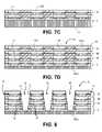
- FIGS. 7A , 7 B and 7 Care cross-sectional views of a second reconstituted wafer structure being formed over the reconstituted wafer structure of FIG. 6 ;
- FIG. 7Dis a cross-sectional view of a stacked microelectronic assembly comprising four reconstituted wafers
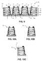
- FIG. 8is a sectional view illustrating a stage of fabrication of stacked microelectronic assembly subsequent to that shown in FIG. 7D in which notches are cut into the assembly;
- FIG. 9is a sectional view of stacked microelectronic assembly after notches have been created, showing the formation of leads on the side walls of the notches;
- FIGS. 10A , 10 B and 10 Cillustrate various embodiments of individual stacked microelectronic units produced from the embodiment of stacked microelectronic assembly of FIG. 9 ;
- FIG. 11is an exemplary embodiment of the individual stacked microelectronic unit of FIG. 10A electrically connected to an interconnection element;
- FIG. 12is a partial top plan view 200 of the stacked microelectronic assembly of FIG. 7D and showing openings made between adjacent microelectronic elements;
- FIG. 13shows a series of side elevation views of structures illustrating initial stages in the formation of stacked microelectronic units according to a second embodiment
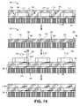
- FIG. 14shows a series of side elevation views of structures illustrating the next stages in the formation of stacked microelectronic units according to the second embodiment
- FIG. 15is a sectional view of the stacked microelectronic assembly produced by the processes illustrated in FIGS. 13 and 14 ;
- FIG. 16is a sectional view of the stacked microelectronic assembly of the second embodiment, after notches have been formed between adjacent microelectronic elements;
- FIG. 17is a top plan view of a portion of the stacked microelectronic assembly of FIG. 16 illustrating the redistribution of electrical signals from a set of contacts at a first edge of a microelectronic element to a second edge;
- FIGS. 18 and 19pictorially illustrate manufacturing apparatus and processes used in the fabrication of the stacked microelectronic units described and shown herein.
- FIGS. 1A-1Cillustrate an array, or a portion of an array, of microelectronic elements.
- FIG. 1Ais a top plan view of wafer 10 , or portion of a wafer 10 , and includes a plurality of microelectronic elements shown as rectangles.
- Wafer 10preferably includes numerous rows of microelectronic elements aligned along an X-axis and a Y-axis, in the form of an array.
- Wafer 10may include any number of microelectronic elements including as little as two or as many as is desirable.
- Wafer 10 in FIG. 1Ahas a top edge 15 , a right edge 13 , a left edge 11 and a bottom edge 17 .
- FIG. 1Ahas a top edge 15 , a right edge 13 , a left edge 11 and a bottom edge 17 .
- FIG. 1Cis an elevated side view of wafer 10 taken along line 1 B ( FIG. 1A ), showing left edge 11 and right edge 13 of wafer 10 .
- FIG. 1Calso shows that each microelectronic element of wafer 10 also has a front face 14 and an oppositely-facing rear face 16 . Note that in FIG. 1C , the front face 14 of wafer 10 has been turned over to face down in the figure.
- each of the microelectronic elements 12 , 12 ′′ (twelve double prime) and 12 ′ (twelve prime)are individually called out in the middle row of wafer 10 .
- the wafercan be in the shape of a circular wafer.
- the wafer 10 or wafer portionis referred to as a “wafer”.
- the microelectronic elementsare formed integral with one another using semiconductor fabrication techniques.
- Each of the microelectronic elements of the waferis typically of the same type.
- the microelectronic elementscan have memory function, logic or processor function or a combination of logic and processor functions, among other possible types.
- each of the microelectronic elementsincludes a flash memory.
- each microelectronic elementcan be a dedicated flash memory chip.
- each microelectronic elementhas a first edge 18 , a second edge 20 , a third edge 19 and a fourth edge 21 .
- a first edge 18 of one microelectronic element 12abuts (or is attached to) second edge 20 of a second and adjacent microelectronic element 12 .
- a third edge 19 ( FIG. 1A ) of one microelectronic element 12is attached to a fourth edge 21 of an adjacent microelectronic element.
- a microelectronic element 12 ′′ positioned in a middle row of the wafer portion 10is bordered by an adjacent microelectronic element at all four edges, as shown in FIG. 1A .
- each of first edge 18 , second edge 20 , third edge 19 and fourth edge 21extends from the front face 14 ( FIG. 1C ) to the rear face 16 ( FIG. 1C ) of the microelectronic element 12 .
- Portions of wafer 10 where adjacent microelectronic elements contact one anotherform saw lanes or strips 23 and 25 where the wafer can be cut without damaging the individual microelectronic elements. For instance, as shown in FIG. 1C , second edge 20 ′ of microelectronic element 12 ′ abuts first edge 18 ′′ of microelectronic element 12 ′′ and forms a saw lane 23 . Similarly, throughout the wafer 10 , saw lanes 23 (shown in FIGS. 1A and 1C ) are located at positions where the microelectronic elements abut one another.
- each microelectronic elementincludes a plurality of contacts 22 ′′ exposed at the respective front face 14 of the microelectronic element 12 .
- the contacts 22can be, for example, bond pads or lands of the microelectronic elements as originally formed in a wafer fabrication facility.
- Each microelectronic element of the uncut wafer 10has a device region 26 (area bounded by dashed lines 27 ) in which active semiconductor devices and typically also passive devices are disposed.
- Each microelectronic elementalso includes a non-device region disposed beyond edges of the device region 26 where no active semiconductor devices or passive devices are disposed. Note that the bounded area of device region 26 is shown by solid lines in FIG.
- a trace 24extends outwardly from each of the contacts 22 to a respective first, second, third or fourth edge 18 , 20 , 19 , and 21 of each individual microelectronic element, crossing between the device region 26 and non-device region.
- trace 24 ′extends outwardly from contact 22 ′ towards the second edge 20 ′ of microelectronic element 12 ′ ( FIG. 1A ).
- the trace 24 ′extends to and contacts trace 24 ′′, which extends outwardly from contact 22 ′′.
- traces 24 ′ and 24 ′′meet at the attachment point of microelectronic elements 12 ′ and 12 ′′ and may actually form a single trace extending between contact 22 ′ and contact 22 ′′.
- the traces 24may be formed in the wafer fabrication facility at the same time or after the contacts 22 of the wafer are fabricated. Alternatively, the traces 24 may be formed by subsequent processing after the wafer 10 leaves the wafer fabrication facility, such as at a facility where processing as described below is performed.
- an assembly including a plurality of stacked microelectronic elementsis fabricated by simultaneously processing a plurality of microelectronic elements en masse. Moreover, processing can be carried out simultaneously as to microelectronic elements which are arranged in form of an array, similar to the processing of an original wafer containing such microelectronic elements.
- FIGS. 2-7Billustrate stages in a method of forming a package or assembly of stacked microelectronic elements in accordance with a first fabrication embodiment. In this embodiment, original wafer 10 is first separated into individual microelectronic elements and then selected ones of the individual microelectronic elements are arranged in form of an array for further processing.
- the array of selected microelectronic elementscan be considered a “reconstituted wafer” which is then available for processing according to wafer-level processing techniques.
- FIG. 2illustrates a stage of fabrication in which an original wafer 10 is separated into individual microelectronic elements 12 by severing, e.g., sawing or scribing wafer 10 along the dicing lanes 23 and 25 ( FIG. 1A ).
- FIG. 3is an elevated side view of reconstituted wafer structure 90 comprising individual microelectronic elements 112 that were selected from the microelectronic elements 12 obtained during the dicing (sawing) stage of FIG. 2 .
- Individual microelectronic elements 112are referred to as the known good die, and are attached in a face down position (i.e., with the front face of the die on which are disposed traces 24 and contacts 22 ) to a carrier 160 using an adhesive 162 .
- a pick-and-place toolcan be used to place each microelectronic element 112 at the proper position on the carrier 160 to form reconstituted wafer structure 90 .
- microelectronic elements that make up each reconstituted wafercan be individually selected. In this way, when some of the microelectronic elements of the original wafer are of known or suspected marginal or failing quality, they need not be processed into stacked assemblies. Rather, those microelectronic elements can be left out of the reconstituted wafer such that the reconstituted wafer contains better quality microelectronic elements. Selection of the microelectronic elements to go into the reconstituted wafer can be made based on various criteria of quality or expected quality based on visual inspection, mechanical or electrical inspection or location of the microelectronic element within the original wafer 10 .
- microelectronic elementsmay in fact be tested electrically before placing each one into position on the reconstituted wafer. Whether the microelectronic elements are selected based on visual inspection, location or electrical test results, the microelectronic elements which are selected for inclusion in the reconstituted wafer can be referred to as “known good” microelectronic elements or “known good die”.
- an etchantis supplied to channels 114 which run between individual ones of the microelectronic elements 112 of reconstituted wafer 90 .
- the etchantis used to remove material from the edges of the microelectronic elements. As a result of this step, portions of the traces 24 at the front face of each microelectronic element become exposed within the channels.
- a dielectric layer 116is then formed over reconstituted wafer structure 90 of FIG. 4 .
- Dielectric layer 116fills channels 114 of reconstituted wafer structure 90 , thereby covering rear faces 118 of the microelectronic elements 112 .
- the dielectric layercan include one or more inorganic dielectric materials such as an oxide, nitride, which may include silicon dioxide, silicon nitride or other dielectric compound of silicon such as SiCOH, among others, or may include an organic dielectric, among which are various polymers such as epoxy, polyimide, among others.
- FIG. 6is a side elevation view of reconstituted wafer structure 110 which is produced by reducing the thickness of each microelectronic element and dielectric layer 116 to a desired thickness by lapping, grinding or polishing reconstituted wafer structure 90 of FIG. 5 from the rear faces 118 of each microelectronic element 112 .
- a next layer of known good dieare then processed using reconstituted wafer 110 as a base or carrier layer.
- a second layer of known good microelectronic elements 112 Aare selected and attached to reconstituted wafer 110 using adhesive layer 162 A which is deposited over reconstituted wafer 110 .
- the second layer of microelectronic elementsis attached in registration with corresponding ones of the first microelectronic elements 112 .
- the second layer of known good microelectronic elements 112 Ais processed in a manner similar to the process shown and described above with reference to FIGS.
- an etchantis supplied to channels 114 A which run between individual ones of the microelectronic elements 112 A of the second reconstituted wafer layer in order to remove material from the edges of microelectronic elements 112 A so as to expose portions of the traces 24 within the channels at the front face of each microelectronic element.
- dielectric layer 116 Ais then formed over the second reconstituted wafer layer of FIG. 7A to fill channels 114 A, thereby covering rear faces 118 of the microelectronic elements 112 A.
- each microelectronic element 112 A and dielectric layer 116 Ais reduced to a desired thickness by lapping, grinding or polishing the second reconstituted wafer layer of FIG. 7B from the rear faces 118 of each microelectronic element 112 A.
- a second reconstituted wafer 110 Ais formed, as shown in FIG. 7C .
- an adhesive layeris formed to overlie microelectronic elements 112 A and a third layer of microelectronic elements 112 B are then attached to that adhesive layer and processed in a manner similar to the process shown and described above with reference to FIGS. 7A through 7C to form third reconstituted wafer 110 B.
- a fourth layer of microelectronic elements 112 Cmay also be formed in a similar manner by forming an adhesive layer over microelectronic elements 112 B and attaching a fourth layer of microelectronic elements 112 C to that adhesive layer and subsequently processing the fourth layer in the same manner as described above to form fourth reconstituted wafer 110 C.
- the thickness of carrier layer 160( FIG. 7C ) may be reduced at this time using any suitable lapping, grinding or polishing process to form reduced carrier layer 160 A.
- a protective layer 164 including a dielectric and which may include an adhesivemay be formed to cover the uppermost layer of microelectronic elements 112 C. Together this processing forms stacked assembly 30 .
- FIG. 8is a sectional view illustrating a stage of fabrication of stacked assembly 30 subsequent to that shown in FIG. 7D .
- the processing illustrated with reference to FIGS. 8-10need not be performed in any particular orientation; the individual microelectronic elements in stacked assembly 30 may have front faces oriented upwardly, downwardly or to a side.
- a plurality of notches 46are cut into the stacked assembly 30 .
- the notches 46are preferably formed using a mechanical cutting instrument not shown in the figures. Examples of such a mechanical cutting instrument can be found in U.S. Pat. Nos. 6,646,289 and 6,972,480, the disclosures of which are hereby incorporated by reference herein.
- notches 46are cut from the stacked assembly 30 at locations between microelectronic elements that are horizontally adjacent in their respective reconstituted wafers 110 , 110 A, 110 B and 110 C. With reference back to FIGS. 1A , 1 B and 1 C, these locations are proximate to respective first edges 18 and second edges 20 of each microelectronic element. Although not shown in the sectional view of FIG. 8 , notches may also be formed in locations that are proximate to respective third edges 19 and fourth edges 21 of each microelectronic element in reconstituted wafers 110 , 110 A, 110 B and 110 C.
- the individual microelectronic elements in each reconstituted wafer 110 , 110 A, 110 B and 110 Care aligned throughout stacked assembly 30 .
- a single cutmay be used to form notches 47 between individual stacked microelectronic elements.
- notches 46do not extend entirely through stacked assembly 30 .
- the microelectronic elements of reconstituted wafer 110remain attached to each other as the various notches 46 do not extend entirely through reduced carrier layer 160 A underlying first reconstituted wafer 110 .
- notches 46are sufficiently wide and deep so as to intersect, and thus expose the edges of, traces 24 (represented as dark thick horizontal lines) that extend out from the contacts disposed on the front faces of the individual microelectronic elements of each reconstituted wafer 110 , 110 A, 110 B and 110 C.
- traces 24represented as dark thick horizontal lines
- notches 46are illustrated having inclined side walls 48 , 50 .
- the side wallsmay be straight, i.e., oriented in a normal direction to a plane defined by the front faces of the microelectronic elements.
- First exposed side edge 170 and second exposed side edge 172 of stacked assembly 30need not be cut to expose edges of the traces because the edges of the traces (represented as dark thick horizontal lines) that extend toward these respective edges are already exposed.
- first and second side edges 170 and 172may be cut so as to create a more symmetrical configuration.
- the other two side edges of stacked assembly 30 not shown in the figuresalso do not have to be cut, although it may be desirable to do so.
- FIG. 9is a sectional view of stacked assembly 30 after notches 46 have been created, showing the formation of leads 66 on the side walls 48 , 50 ( FIG. 8 ) of notches 46 .
- Leads 66may be formed by any suitable metal deposition technique, for example, a process that includes sputtering, three-dimensional lithography and electroplating. Additional processes may also be employed. One such process is disclosed in U.S. Pat. No. 5,716,759, the disclosure of which is hereby incorporated by reference herein.
- lead formationmay comprise the depositing a metal layer across the entire length and depth of a notch 46 , and then etching the metal away in areas where there are no exposed edges of traces 24 .
- each of a set of individual leads 66extends within a notch 46 at the location of the exposed edges of a set of aligned traces 24 of reconstituted wafers 110 , 110 A, 110 B and 110 C, thereby establishing electrical contact with the exposed edges of that set of traces 24 .
- leads 66include end lead portion 75 which extends past the side wall of each notch 46 onto protective layer 164 positioned above reconstituted wafer 110 C. If protective layer 164 is not provided, end lead portion 75 extends past the side wall of each notch 46 onto the rear face of the individual microelectronic elements that form reconstituted wafer 110 C. Pads or solder bumps 74 may be formed to be in contact with end lead portion 75 as shown.
- each lead 66is in contact with all of the edges of the traces 24 exposed at a respective side wall of notch 46 .
- a lead 66may be in electrical connection with fewer than all of the traces 24 of the stacked microelectronic elements in a set of reconstituted wafers 110 , 10 A, 110 B and 11 C when traces 24 disposed on one microelectronic element in one reconstituted wafer layer are not in exact alignment or lie in different planes than traces 24 disposed on microelectronic elements in a second, third or fourth reconstituted wafer layer.
- reduced carrier layer 160 A of stacked assembly 30may be severed by mechanically cutting or, alternatively, scribing and breaking reconstituted wafer 110 at locations 90 proximate to notches 46 . In this way, a plurality of individual units are produced, with each individual unit containing a plurality of microelectronic elements stacked one upon another.
- FIGS. 10A and 10Billustrate two embodiments of individual units 80 and 81 from the embodiment of stacked assembly 30 of FIG. 9 with inclined sidewalls in which the severing, or singulation, process at locations 90 of FIG. 9 achieves different profiles, depending on the method used and the precision of the cutting instrument, if one is used.
- individual units produced from a stack of microelectronic elementsneed not have inclined sidewalls; single units with sidewalls normal to reduced carrier layer 160 A are not illustrated in the figures.
- individual units produced from the stacked reconstituted wafers of microelectronic elements located at the ends of stacked assembly 30may or may not have inclined sidewalls all around.
- FIG. 10Cillustrates individual unit 82 produced after singulation from the embodiment of stacked assembly 30 of FIG. 9 that includes left edge 170 .
- FIG. 11is an exemplary embodiment of stacked assembly 80 , shown inverted from the view in FIG. 10A , electrically connected via solder bumps 74 to an interconnection element 210 , e.g., a dielectric element, substrate, circuit panel or other element having terminals 84 , 86 and conductive wiring therein.
- interconnection element 210e.g., a dielectric element, substrate, circuit panel or other element having terminals 84 , 86 and conductive wiring therein.
- One or more additional microelectronic elements 230can be attached to the face of assembly 80 opposite the face comprising solder bumps 74 and electrically interconnected by bond wires 88 to terminals 84 of the interconnection element 210 .
- microelectronic element 230may include one or more additional microelectronic elements which supplement the function of the stacked assembly, such as, by way of example and not intended to be exhaustive, a microcontroller.
- Microelectronic element 230may include one or more redundancy elements for substitution with one or more of the individual microelectronic elements in stacked individual unit 80 , in case of a problem with such microelectronic element.
- the stacked individual unit 80may be incorporated into microprocessors, and RF units among other assemblies.
- One or more stacked units 80may incorporate particular types of microelectronic elements such as flash memory or dynamic random access memory (DRAM) units and be incorporated in various units including memory modules, memory cards, and the like.
- DRAMdynamic random access memory
- electrical access to conductive traces 24 in all reconstituted wafer layers 110 , 110 A, 110 B and 110 Cis achieved by cutting notches 46 into stacked assembly 30 in the manner shown in these figures and described above with reference thereto, in order to expose the edges of conductive traces 24 to the later-applied leads 66 ( FIG. 9 ).
- Lead formationis achieved by using a suitable metal deposition technique to deposit a metal layer onto the surfaces of each notch 46 .
- Such metal deposition techniquesmay require metal etching to form leads that provide electrical access to only the exposed edges of traces disposed on the front faces of the microelectronic elements that are vertically aligned in the reconstituted wafer layers 110 C, 110 B, 110 A and 110 .
- electrical accessmay be made to conductive traces 24 in reconstituted wafer layers 110 , 110 A, 110 B and 110 C by making openings, or vias, into stacked assembly 30 at the locations of the traces, using any suitable drilling technique, such as a laser drilling technique.
- FIG. 12is a partial top plan view 200 of stacked assembly 30 of FIG. 7D looking down at top reconstituted wafer 110 C, assuming for purposes of this discussion that protective layer 164 is at least partially transparent or is not present in this embodiment.
- Openings, or vias, 228are represented by small grey circles; while not labeled as such, it is to be understood from the figure that each grey circle represented is an opening 228 .
- FIG. 12is a partial top plan view 200 of stacked assembly 30 of FIG. 7D looking down at top reconstituted wafer 110 C, assuming for purposes of this discussion that protective layer 164 is at least partially transparent or is not present in this embodiment.
- Openings, or vias, 228are represented by small grey circles; while not labeled
- representative ones of openings 228are formed in saw lanes 218 and 220 of reconstituted wafer 110 C between adjacent microelectronic elements and extend through stacked assembly 30 to reach to reconstituted wafer 110 .
- Each opening 228thus exposes the edges of all of the traces 24 disposed on the front faces of each of the pairs of vertically aligned and adjacent microelectronic elements in all of reconstituted wafer layers 110 C, 110 B, 110 A and 110 .
- the individual openings 228are plated using a suitable metal deposition technique, after which a singulation (e.g., dicing) process produces individual stacked microelectronic units from stacked assembly 30 similar to those shown in FIGS. 10A , 10 B and 10 C.
- electrical accessmay be made to all or selective ones of the conductive traces 24 in selective ones of reconstituted wafer layers 110 , 110 A, 110 B and 110 C by making openings to selected depths into stacked assembly 30 at selected locations.
- FIGS. 13-17illustrate another embodiment for forming stacked microelectronic units.
- FIG. 13shows a series of side elevation views of structures illustrating initial stages in the formation of stacked microelectronic units according to this embodiment.
- Microelectronic elements 32 having bond pads 22 connected to traces 24are separated from an original wafer (not shown) along saw lines 23 .
- Selected microelectronic elements 312e.g., known good die
- carrier 160is attached to carrier 160 using adhesive layer 162 to form reconstituted wafer structure 390 . Then, in a manner similar to the processes described with respect to FIGS.
- an etchantis supplied to channels 114 which run between individual ones of the microelectronic elements 312 to remove material from the edges of the microelectronic elements in order to expose within channels 114 portions of the traces 24 at the front face of each microelectronic element 312 .
- a dielectric layer 116is then formed over reconstituted wafer structure 390 to fill channels 114 , thereby covering rear faces 118 of the microelectronic elements 312 and producing reconstituted wafer structure 392 .
- FIG. 14shows a series of side elevation views of structures illustrating the next stages in the formation of stacked microelectronic units according to this embodiment.
- Reconstituted wafer structure 392 of FIG. 13is then thinned to produce reconstituted wafer 310 by reducing the thickness of each microelectronic element and dielectric layer 116 to a desired thickness by lapping, grinding or polishing reconstituted wafer structure 392 from the rear faces 118 of each microelectronic element 312 .
- Arrows 350mark the lateral position of each edge 340 of each microelectronic element of reconstituted wafer 310 .
- the microelectronic elements 312 A needed to form a second reconstituted wafer 310 Aare bonded to reconstituted wafer 310 such that an edge 340 A of a microelectronic element 312 A of the second reconstituted wafer structure to be formed occurs at position 350 A which is offset in a lateral direction 360 from the edge 340 of the first reconstituted wafer 310 .
- overlying microelectronic elements 312 Aeach has an area overlapping an area of the underlying microelectronic element 312 to which it is bonded, and each has an edge 340 A that is displaced in the lateral direction 360 from the edge 340 of the underlying microelectronic element 312 .
- An exemplary distance of the lateral offset between edges of vertically adjacent overlapping microelectronic elementscan range from a few microns to tens of microns or more.
- second reconstituted wafer 310 Ais completed with the etching process, the application of the dielectric layer, and thinning process shown in FIG. 13 with respect to reconstituted wafer 310 , omitted in FIG. 14 .
- the sub-processes shown in FIG. 14are repeated for forming a third reconstituted wafer 310 B containing microelectronic element 312 B and a fourth reconstituted wafer 310 C containing microelectronic element 312 C to form the stacked assembly 330 shown in FIG. 15 .
- notches 346are then cut between adjacent elements to expose the edges of the traces disposed on the front faces of the microelectronic elements in each reconstituted wafer 310 , 310 A, 310 B and 310 C.
- An advantage of forming the stacked assembly in this manneris that process tolerances can improve for forming leads 366 ( FIG. 16 ) adjacent to the exposed edges of the traces at the sidewalls of notch 46 .
- the lateral displacement of each succeeding overlapping microelectronic element in the stacked assemblyallows for slope in the sidewalls of each notch 346 formed therein. Increased lateral displacement allows the sidewalls of each notch 346 to be more heavily sloped, i.e., at a greater angle from the vertical.
- “Vertical”is defined herein as a normal angle to the plane defined by the contact-bearing surface of a microelectronic element, e.g., element 312 .
- the notching operationperformed, e.g., by cutting or laser drilling exposes trace edges even when the length of such traces is limited.
- traces 324can have very limited length.
- a redistribution layer including additional traces 326can be provided which extends between the pads at edge 342 and outwardly beyond a third edge 344 of the microelectronic element 312 .
- overlapping microelectronic elements of each successively stacked reconstituted wafer 310 , 310 A, 310 B and 310 Ccan be offset as well in a direction 362 . In this way, leads can be formed in notches which expose traces 326 along the third edges 344 of the overlapping microelectronic elements, and process tolerance can also be improved for forming such leads.
- FIGS. 18 and 19are illustrations of apparatus employed in the manufacture of assemblies of the types discussed herein.
- a conventional wafer fabrication facility 680provides complete wafers 681 , of the type partially shown in FIGS. 1A and 1B .
- Individual microelectronic elements or chips 682are bonded on their active surfaces to a carrier layer or protective layer 683 by bonding apparatus 685 , such as by way of a layer of adhesive, e.g., epoxy (not shown).
- the apparatus 685preferably has facilities for rotation and distribution of the layer of adhesive over the non-active surface (generally the rear surface), as well of the thus formed reconstituted wafer so as to obtain even distribution of the epoxy.
- the thus formed reconstituted wafer 686is thinned at its non-active surface as by a grinding apparatus 684 using an abrasive 687 .
- the waferis then etched at its non-active surface, preferably by photolithography, such as by using conventional spin-coated photoresist, using a mask exposure machine 692 for the exposure of light sensitive photoresist 690 through the mask 691 and later etching the silicon in a bath 693 using solution 699 .
- the etched waferis bonded on the non-active side to an adhesive or protective layer 1000 , which can be epoxy or other adhesive by bonding apparatus 694 , which may be essentially the same as apparatus 685 , to produce a doubly bonded wafer sandwich.
- the wafermay then by bonded to a second or more wafers.
- Notching apparatus 695partially cuts the stacked assembly in a method of forming a stacked package as described above with reference to FIGS. 2-9 .
- the notched stacked assemblythen is subjected to anti-corrosion treatment in a bath 696 , containing a chromating solution 698 .
- a chemical etching apparatus(not shown) may be used to form notches exposing one or more traces or openings exposing the traces of respective microelectronic elements.
- Conductive layer deposition apparatus 700( FIG. 19 ), which operates by vacuum deposition techniques, is employed to produce a conductive layer on one or more surfaces of each die of the wafers. Configuration of the contact strips or lead bridges is carried out preferably by using conventional electro-deposited photoresist 701 .
- the photoresist 701is applied to the stacked assembly 707 of reconstituted wafers in a photoresist bath assembly 702 .
- the photoresist 701is preferably light configured by a UV exposure system 704 , which may be identical to system 692 , using a mask 705 to define suitable etching patterns.
- the photoresistis then developed in a development bath 706 , and then the wafer is etched in a metal solution 708 located in an etching bath 710 , thus providing a conductor configuration.
- the exposed conductive stripsare then plated, preferably by electroless plating apparatus 712 .
- the stacked wafersare then diced into individual prepackaged integrated devices as described above with reference to FIGS. 9 and 10 .
- the dicing blade 714should be a diamond resinoid blade having a thickness of about 4 to about 12 mils, such thickness preferably corresponding to the width of the saw lanes 23 , 25 ( FIG. 1A ).
Landscapes
- Engineering & Computer Science (AREA)
- Microelectronics & Electronic Packaging (AREA)
- Power Engineering (AREA)
- Computer Hardware Design (AREA)
- Physics & Mathematics (AREA)
- Condensed Matter Physics & Semiconductors (AREA)
- General Physics & Mathematics (AREA)
- Manufacturing & Machinery (AREA)
- Semiconductor Memories (AREA)
- Wire Bonding (AREA)
- Internal Circuitry In Semiconductor Integrated Circuit Devices (AREA)
Abstract
Description
- The subject matter of the present application relates to microelectronic packages, or assemblies, comprised of stacked microelectronic elements and to methods of fabricating them, for example, by processing applied simultaneously to a plurality of microelectronic elements arranged in an array.
- Microelectronic elements, such as semiconductor chips, are flat bodies with contacts disposed on the front surface that are connected to the internal electrical circuitry of the element itself. Microelectronic elements are typically packaged with substrates to form microelectronic packages, or assemblies, having terminals that are electrically connected to the element's contacts. The package or assembly may then be connected to test equipment to determine whether the packaged device conforms to a desired performance standard. Once tested, the package may be connected to a larger circuit, e.g., a circuit in an electronic product such as a computer or a cell phone.
- Microelectronic packages or assemblies also include wafer level packages, which provide a package for a microelectronic component that is fabricated while the die are still in a wafer form. The wafer is subject to a number of additional process steps to form the package structure and the wafer is then diced to free the individual die. Wafer level processing may provide a cost savings advantage. Furthermore, the package footprint can be identical to the die size, resulting in very efficient utilization of area on a printed circuit board (PCB) to which the die will eventually be attached. As a result of these features, die packaged in this manner are commonly referred to as wafer-level chip scale packages (WLCSP).
- In order to save space certain conventional designs have stacked multiple microelectronic chips or elements within a package or assembly. This allows the package to occupy a surface area on a substrate that is less than the total surface area of all the chips in the stack added together. Development efforts in this technology focus on producing wafer-level assemblies that are reliable, or thin, or testable, or which are economical to manufacture, or have a combination of such characteristics.
- A method is provided for fabricating a stacked microelectronic assembly from a structure which includes a plurality of first microelectronic elements having front faces bonded to a carrier. Each first microelectronic element may have a plurality of first edges and a plurality of first traces extending along the front face towards the first edges. After exposing the first traces, a dielectric layer is formed over the plurality of first microelectronic elements. After thinning the dielectric layer, a plurality of second microelectronic elements are aligned and joined with the structure such that front faces of the second microelectronic elements are adjacent to rear faces of the plurality of first microelectronic elements. Processing is repeated to form the desirable number of layers of microelectronic elements. In one embodiment, the stacked layers of microelectronic elements may be notched at dicing lines to expose edges of traces, which may then be electrically connected to leads formed in the notches. Individual stacked microelectronic units may be separated from the stacked microelectronic assembly by any suitable dicing, sawing or breaking technique.
- The structure and methods of fabrication of the microelectronic devices described herein are best understood when the following description of several illustrated embodiments is read in connection with the accompanying drawings wherein the same reference numbers are used throughout the drawings to refer to the same or like parts. The drawings are not necessarily to scale; emphasis has instead been placed upon illustrating the structural and fabrication principles of the described embodiments. The drawings include:
FIG. 1A is a top plan view of a wafer, or portion of a wafer, comprising microelectronic elements;FIG. 1B is an enlarged portion of one of the microelectronic elements disposed on the wafer ofFIG. 1A ;FIG. 1C is a side elevation view of a portion of the wafer ofFIG. 1A taken atline 1B ofFIG. 1A ;FIG. 2 is a side elevation view of several individual microelectronic elements separated from the wafer ofFIG. 1A ;FIG. 3 is an elevated side view of a reconstituted wafer structure comprising individual microelectronic elements selected from the microelectronic elements ofFIG. 2 ;FIG. 4 is a cross-sectional view of the reconstituted wafer structure ofFIG. 3 after an etchant is supplied to channels running between individual ones of the microelectronic elements to remove material from the edges of the microelectronic elements;FIG. 5 is a cross-sectional view of the reconstituted wafer structure ofFIG. 4 after a dielectric layer is formed over the structure;FIG. 6 is a cross-sectional view of the reconstituted wafer structure ofFIG. 5 after the dielectric layer and microelectronic elements have been thinned to a desired height;FIGS. 7A ,7B and7C are cross-sectional views of a second reconstituted wafer structure being formed over the reconstituted wafer structure ofFIG. 6 ;FIG. 7D is a cross-sectional view of a stacked microelectronic assembly comprising four reconstituted wafers;FIG. 8 is a sectional view illustrating a stage of fabrication of stacked microelectronic assembly subsequent to that shown inFIG. 7D in which notches are cut into the assembly;FIG. 9 is a sectional view of stacked microelectronic assembly after notches have been created, showing the formation of leads on the side walls of the notches;FIGS. 10A ,10B and10C illustrate various embodiments of individual stacked microelectronic units produced from the embodiment of stacked microelectronic assembly ofFIG. 9 ;FIG. 11 is an exemplary embodiment of the individual stacked microelectronic unit ofFIG. 10A electrically connected to an interconnection element;FIG. 12 is a partialtop plan view 200 of the stacked microelectronic assembly ofFIG. 7D and showing openings made between adjacent microelectronic elements;FIG. 13 shows a series of side elevation views of structures illustrating initial stages in the formation of stacked microelectronic units according to a second embodiment;FIG. 14 shows a series of side elevation views of structures illustrating the next stages in the formation of stacked microelectronic units according to the second embodiment;FIG. 15 is a sectional view of the stacked microelectronic assembly produced by the processes illustrated inFIGS. 13 and 14 ;FIG. 16 is a sectional view of the stacked microelectronic assembly of the second embodiment, after notches have been formed between adjacent microelectronic elements;FIG. 17 is a top plan view of a portion of the stacked microelectronic assembly ofFIG. 16 illustrating the redistribution of electrical signals from a set of contacts at a first edge of a microelectronic element to a second edge; andFIGS. 18 and 19 pictorially illustrate manufacturing apparatus and processes used in the fabrication of the stacked microelectronic units described and shown herein.FIGS. 1A-1C illustrate an array, or a portion of an array, of microelectronic elements.FIG. 1A is a top plan view ofwafer 10, or portion of awafer 10, and includes a plurality of microelectronic elements shown as rectangles.Wafer 10 preferably includes numerous rows of microelectronic elements aligned along an X-axis and a Y-axis, in the form of an array.Wafer 10 may include any number of microelectronic elements including as little as two or as many as is desirable.Wafer 10 inFIG. 1A has atop edge 15, aright edge 13, aleft edge 11 and abottom edge 17.FIG. 1C is an elevated side view ofwafer 10 taken alongline 1B (FIG. 1A ), showing leftedge 11 andright edge 13 ofwafer 10.FIG. 1C also shows that each microelectronic element ofwafer 10 also has afront face 14 and an oppositely-facingrear face 16. Note that inFIG. 1C , thefront face 14 ofwafer 10 has been turned over to face down in the figure.- In
FIG. 1A , threemicroelectronic elements wafer 10. The wafer can be in the shape of a circular wafer. Hereinafter, for ease of reference, thewafer 10 or wafer portion is referred to as a “wafer”. The microelectronic elements are formed integral with one another using semiconductor fabrication techniques. Each of the microelectronic elements of the wafer is typically of the same type. The microelectronic elements can have memory function, logic or processor function or a combination of logic and processor functions, among other possible types. In a particular example, each of the microelectronic elements includes a flash memory. For example, each microelectronic element can be a dedicated flash memory chip. - With reference to
microelectronic element 12 ofFIG. 1A , each microelectronic element has afirst edge 18, asecond edge 20, athird edge 19 and afourth edge 21. Whenmicroelectronic element 12 is still part of the array ofwafer 10, afirst edge 18 of onemicroelectronic element 12 abuts (or is attached to)second edge 20 of a second and adjacentmicroelectronic element 12. Similarly, a third edge19 (FIG. 1A ) of onemicroelectronic element 12 is attached to afourth edge 21 of an adjacent microelectronic element. Thus, amicroelectronic element 12″ positioned in a middle row of thewafer portion 10 is bordered by an adjacent microelectronic element at all four edges, as shown inFIG. 1A . Whenmicroelectronic element 12 is entirely separated from wafer10 (e.g., singulated thereform), it can be seen that each offirst edge 18,second edge 20,third edge 19 andfourth edge 21 extends from the front face14 (FIG. 1C ) to the rear face16 (FIG. 1C ) of themicroelectronic element 12. - Portions of
wafer 10 where adjacent microelectronic elements contact one another form saw lanes or strips23 and25 where the wafer can be cut without damaging the individual microelectronic elements. For instance, as shown inFIG. 1C ,second edge 20′ ofmicroelectronic element 12′ abutsfirst edge 18″ ofmicroelectronic element 12″ and forms asaw lane 23. Similarly, throughout thewafer 10, saw lanes23 (shown inFIGS. 1A and 1C ) are located at positions where the microelectronic elements abut one another. - With reference to
microelectronic element 12″ ofFIG. 1B , each microelectronic element includes a plurality ofcontacts 22″ exposed at the respective front face14 of themicroelectronic element 12. Thecontacts 22 can be, for example, bond pads or lands of the microelectronic elements as originally formed in a wafer fabrication facility. Each microelectronic element of theuncut wafer 10 has a device region26 (area bounded by dashed lines27) in which active semiconductor devices and typically also passive devices are disposed. Each microelectronic element also includes a non-device region disposed beyond edges of thedevice region 26 where no active semiconductor devices or passive devices are disposed. Note that the bounded area ofdevice region 26 is shown by solid lines inFIG. 1C . Atrace 24 extends outwardly from each of thecontacts 22 to a respective first, second, third orfourth edge device region 26 and non-device region. For example, with reference toFIG. 1B , trace24′ extends outwardly fromcontact 22′ towards thesecond edge 20′ ofmicroelectronic element 12′ (FIG. 1A ). Thetrace 24′ extends to and contacts trace24″, which extends outwardly fromcontact 22″. Thus, traces24′ and24″ meet at the attachment point ofmicroelectronic elements 12′ and12″ and may actually form a single trace extending betweencontact 22′ and contact22″. However, it is not required that the traces actually contact one another. Similar structures may be included for all adjacentmicroelectronic elements 12. Thetraces 24 may be formed in the wafer fabrication facility at the same time or after thecontacts 22 of the wafer are fabricated. Alternatively, thetraces 24 may be formed by subsequent processing after thewafer 10 leaves the wafer fabrication facility, such as at a facility where processing as described below is performed. - In one stacked assembly fabrication embodiment, an assembly including a plurality of stacked microelectronic elements is fabricated by simultaneously processing a plurality of microelectronic elements en masse. Moreover, processing can be carried out simultaneously as to microelectronic elements which are arranged in form of an array, similar to the processing of an original wafer containing such microelectronic elements.
FIGS. 2-7B illustrate stages in a method of forming a package or assembly of stacked microelectronic elements in accordance with a first fabrication embodiment. In this embodiment,original wafer 10 is first separated into individual microelectronic elements and then selected ones of the individual microelectronic elements are arranged in form of an array for further processing. In this embodiment, the array of selected microelectronic elements can be considered a “reconstituted wafer” which is then available for processing according to wafer-level processing techniques.FIG. 2 illustrates a stage of fabrication in which anoriginal wafer 10 is separated into individualmicroelectronic elements 12 by severing, e.g., sawing or scribingwafer 10 along the dicinglanes 23 and25 (FIG. 1A ).FIG. 3 is an elevated side view of reconstitutedwafer structure 90 comprising individualmicroelectronic elements 112 that were selected from themicroelectronic elements 12 obtained during the dicing (sawing) stage ofFIG. 2 . Individualmicroelectronic elements 112 are referred to as the known good die, and are attached in a face down position (i.e., with the front face of the die on which are disposedtraces 24 and contacts22) to acarrier 160 using an adhesive162. A pick-and-place tool can be used to place eachmicroelectronic element 112 at the proper position on thecarrier 160 to form reconstitutedwafer structure 90. - An advantage of processing reconstituted wafers rather than the
original wafer 10 is that the microelectronic elements that make up each reconstituted wafer can be individually selected. In this way, when some of the microelectronic elements of the original wafer are of known or suspected marginal or failing quality, they need not be processed into stacked assemblies. Rather, those microelectronic elements can be left out of the reconstituted wafer such that the reconstituted wafer contains better quality microelectronic elements. Selection of the microelectronic elements to go into the reconstituted wafer can be made based on various criteria of quality or expected quality based on visual inspection, mechanical or electrical inspection or location of the microelectronic element within theoriginal wafer 10. In a particular embodiment, microelectronic elements may in fact be tested electrically before placing each one into position on the reconstituted wafer. Whether the microelectronic elements are selected based on visual inspection, location or electrical test results, the microelectronic elements which are selected for inclusion in the reconstituted wafer can be referred to as “known good” microelectronic elements or “known good die”. - Next, as illustrated in
FIG. 4 , an etchant is supplied tochannels 114 which run between individual ones of themicroelectronic elements 112 of reconstitutedwafer 90. The etchant is used to remove material from the edges of the microelectronic elements. As a result of this step, portions of thetraces 24 at the front face of each microelectronic element become exposed within the channels. - As illustrated in
FIG. 5 , adielectric layer 116 is then formed over reconstitutedwafer structure 90 ofFIG. 4 .Dielectric layer 116 fillschannels 114 of reconstitutedwafer structure 90, thereby covering rear faces118 of themicroelectronic elements 112. The dielectric layer can include one or more inorganic dielectric materials such as an oxide, nitride, which may include silicon dioxide, silicon nitride or other dielectric compound of silicon such as SiCOH, among others, or may include an organic dielectric, among which are various polymers such as epoxy, polyimide, among others.FIG. 6 is a side elevation view of reconstitutedwafer structure 110 which is produced by reducing the thickness of each microelectronic element anddielectric layer 116 to a desired thickness by lapping, grinding or polishing reconstitutedwafer structure 90 ofFIG. 5 from the rear faces118 of eachmicroelectronic element 112. - With reference to
FIG. 7A , a next layer of known good die are then processed usingreconstituted wafer 110 as a base or carrier layer. A second layer of known goodmicroelectronic elements 112A are selected and attached to reconstitutedwafer 110 usingadhesive layer 162A which is deposited over reconstitutedwafer 110. Desirably, the second layer of microelectronic elements is attached in registration with corresponding ones of the firstmicroelectronic elements 112. The second layer of known goodmicroelectronic elements 112A is processed in a manner similar to the process shown and described above with reference toFIGS. 4 through 6 ; that is, an etchant is supplied tochannels 114A which run between individual ones of themicroelectronic elements 112A of the second reconstituted wafer layer in order to remove material from the edges ofmicroelectronic elements 112A so as to expose portions of thetraces 24 within the channels at the front face of each microelectronic element. As shown inFIG. 7B ,dielectric layer 116A is then formed over the second reconstituted wafer layer ofFIG. 7A to fillchannels 114A, thereby covering rear faces118 of themicroelectronic elements 112A. Then the thickness of eachmicroelectronic element 112A anddielectric layer 116A is reduced to a desired thickness by lapping, grinding or polishing the second reconstituted wafer layer ofFIG. 7B from the rear faces118 of eachmicroelectronic element 112A. At the conclusion of this processing, a secondreconstituted wafer 110A is formed, as shown inFIG. 7C . - Thereafter, with reference to
FIG. 7D , if it is desired to add further layers of microelectronic elements to the stack of microelectronic elements ofFIG. 7C , an adhesive layer is formed to overliemicroelectronic elements 112A and a third layer ofmicroelectronic elements 112B are then attached to that adhesive layer and processed in a manner similar to the process shown and described above with reference toFIGS. 7A through 7C to form thirdreconstituted wafer 110B. A fourth layer ofmicroelectronic elements 112C may also be formed in a similar manner by forming an adhesive layer overmicroelectronic elements 112B and attaching a fourth layer ofmicroelectronic elements 112C to that adhesive layer and subsequently processing the fourth layer in the same manner as described above to form fourthreconstituted wafer 110C. The thickness of carrier layer160 (FIG. 7C ) may be reduced at this time using any suitable lapping, grinding or polishing process to form reducedcarrier layer 160A. In addition, aprotective layer 164 including a dielectric and which may include an adhesive (not separately shown in the figure) may be formed to cover the uppermost layer ofmicroelectronic elements 112C. Together this processing forms stackedassembly 30. FIG. 8 is a sectional view illustrating a stage of fabrication of stackedassembly 30 subsequent to that shown inFIG. 7D . The processing illustrated with reference toFIGS. 8-10 need not be performed in any particular orientation; the individual microelectronic elements in stackedassembly 30 may have front faces oriented upwardly, downwardly or to a side. Referring toFIG. 8 , a plurality ofnotches 46 are cut into the stackedassembly 30. Thenotches 46 are preferably formed using a mechanical cutting instrument not shown in the figures. Examples of such a mechanical cutting instrument can be found in U.S. Pat. Nos. 6,646,289 and 6,972,480, the disclosures of which are hereby incorporated by reference herein. Alternatively, a laser drilling technique can be used to formnotches 46. As compared toFIG. 7D and as shown inFIG. 8 ,notches 46 are cut from the stackedassembly 30 at locations between microelectronic elements that are horizontally adjacent in their respectivereconstituted wafers FIGS. 1A ,1B and1C, these locations are proximate to respectivefirst edges 18 andsecond edges 20 of each microelectronic element. Although not shown in the sectional view ofFIG. 8 , notches may also be formed in locations that are proximate to respectivethird edges 19 andfourth edges 21 of each microelectronic element inreconstituted wafers - In the embodiment shown in
FIG. 8 , the individual microelectronic elements in eachreconstituted wafer assembly 30. Thus, a single cut may be used to form notches47 between individual stacked microelectronic elements. In the embodiment shown inFIG. 8 ,notches 46 do not extend entirely through stackedassembly 30. For instance, as shown inFIG. 8 , the microelectronic elements of reconstitutedwafer 110 remain attached to each other as thevarious notches 46 do not extend entirely through reducedcarrier layer 160A underlying firstreconstituted wafer 110. However,notches 46 are sufficiently wide and deep so as to intersect, and thus expose the edges of, traces24 (represented as dark thick horizontal lines) that extend out from the contacts disposed on the front faces of the individual microelectronic elements of eachreconstituted wafer FIG. 8 ,notches 46 are illustrated having inclinedside walls - First exposed
side edge 170 and second exposedside edge 172 of stackedassembly 30 need not be cut to expose edges of the traces because the edges of the traces (represented as dark thick horizontal lines) that extend toward these respective edges are already exposed. In another embodiment not illustrated in a figure herein, first and second side edges170 and172 may be cut so as to create a more symmetrical configuration. Similarly, the other two side edges of stackedassembly 30 not shown in the figures also do not have to be cut, although it may be desirable to do so. FIG. 9 is a sectional view of stackedassembly 30 afternotches 46 have been created, showing the formation ofleads 66 on theside walls 48,50 (FIG. 8 ) ofnotches 46. Leads66 may be formed by any suitable metal deposition technique, for example, a process that includes sputtering, three-dimensional lithography and electroplating. Additional processes may also be employed. One such process is disclosed in U.S. Pat. No. 5,716,759, the disclosure of which is hereby incorporated by reference herein. Depending on the particular process used, lead formation may comprise the depositing a metal layer across the entire length and depth of anotch 46, and then etching the metal away in areas where there are no exposed edges oftraces 24. When the lead formation process is completed, each of a set of individual leads66 extends within anotch 46 at the location of the exposed edges of a set of aligned traces24 of reconstitutedwafers traces 24. In the embodiment shown inFIG. 9 , leads66 includeend lead portion 75 which extends past the side wall of eachnotch 46 ontoprotective layer 164 positioned above reconstitutedwafer 110C. Ifprotective layer 164 is not provided,end lead portion 75 extends past the side wall of eachnotch 46 onto the rear face of the individual microelectronic elements that form reconstitutedwafer 110C. Pads or solder bumps74 may be formed to be in contact withend lead portion 75 as shown.- With continued reference to
FIG. 9 , when traces24 disposed on the face of individual microelectronic elements in eachreconstituted wafer traces 24 exposed at a respective side wall ofnotch 46. However, in another embodiment, a lead66 may be in electrical connection with fewer than all of thetraces 24 of the stacked microelectronic elements in a set of reconstitutedwafers traces 24 disposed on microelectronic elements in a second, third or fourth reconstituted wafer layer. - With continued reference to
FIG. 9 , afternotches 46 and conductive elements including leads66,end lead portions 75 and solder bumps74 are formed on stackedassembly 30, reducedcarrier layer 160A of stackedassembly 30 may be severed by mechanically cutting or, alternatively, scribing and breakingreconstituted wafer 110 atlocations 90 proximate tonotches 46. In this way, a plurality of individual units are produced, with each individual unit containing a plurality of microelectronic elements stacked one upon another. FIGS. 10A and 10B illustrate two embodiments ofindividual units assembly 30 ofFIG. 9 with inclined sidewalls in which the severing, or singulation, process atlocations 90 ofFIG. 9 achieves different profiles, depending on the method used and the precision of the cutting instrument, if one is used. As noted above, individual units produced from a stack of microelectronic elements need not have inclined sidewalls; single units with sidewalls normal toreduced carrier layer 160A are not illustrated in the figures. Also noted above, individual units produced from the stacked reconstituted wafers of microelectronic elements located at the ends of stackedassembly 30 may or may not have inclined sidewalls all around.FIG. 10C illustratesindividual unit 82 produced after singulation from the embodiment of stackedassembly 30 ofFIG. 9 that includesleft edge 170.- Any one of individual stacked
assemblies FIG. 10A ,10B or10C can be electrically connected to other electronic elements or substrates.FIG. 11 is an exemplary embodiment of stackedassembly 80, shown inverted from the view inFIG. 10A , electrically connected via solder bumps74 to aninterconnection element 210, e.g., a dielectric element, substrate, circuit panel or otherelement having terminals microelectronic elements 230 can be attached to the face ofassembly 80 opposite the face comprising solder bumps74 and electrically interconnected bybond wires 88 toterminals 84 of theinterconnection element 210. Examples ofmicroelectronic element 230 may include one or more additional microelectronic elements which supplement the function of the stacked assembly, such as, by way of example and not intended to be exhaustive, a microcontroller.Microelectronic element 230 may include one or more redundancy elements for substitution with one or more of the individual microelectronic elements in stackedindividual unit 80, in case of a problem with such microelectronic element. In a particular embodiment, the stackedindividual unit 80 may be incorporated into microprocessors, and RF units among other assemblies. One or morestacked units 80 may incorporate particular types of microelectronic elements such as flash memory or dynamic random access memory (DRAM) units and be incorporated in various units including memory modules, memory cards, and the like. Other exemplary arrangements for electrically connecting stackedindividual unit 80 to an interconnection element, and for mounting additional microelectronic elements to stackedindividual unit 80 are shown and described in commonly owned U.S. patent application Ser. No. 11/787,209 filed Apr. 13, 2007, the disclosure of which is hereby incorporated herein by reference. - With reference to
FIGS. 7D and 8 , electrical access toconductive traces 24 in all reconstituted wafer layers110,110A,110B and110C is achieved by cuttingnotches 46 into stackedassembly 30 in the manner shown in these figures and described above with reference thereto, in order to expose the edges ofconductive traces 24 to the later-applied leads66 (FIG. 9 ). Lead formation is achieved by using a suitable metal deposition technique to deposit a metal layer onto the surfaces of eachnotch 46. Such metal deposition techniques may require metal etching to form leads that provide electrical access to only the exposed edges of traces disposed on the front faces of the microelectronic elements that are vertically aligned in the reconstituted wafer layers110C,110B,110A and110. - In another embodiment, electrical access may be made to
conductive traces 24 in reconstituted wafer layers110,110A,110B and110C by making openings, or vias, into stackedassembly 30 at the locations of the traces, using any suitable drilling technique, such as a laser drilling technique.FIG. 12 is a partialtop plan view 200 of stackedassembly 30 ofFIG. 7D looking down at topreconstituted wafer 110C, assuming for purposes of this discussion thatprotective layer 164 is at least partially transparent or is not present in this embodiment. Openings, or vias,228 are represented by small grey circles; while not labeled as such, it is to be understood from the figure that each grey circle represented is anopening 228. InFIG. 12 , representative ones ofopenings 228 are formed insaw lanes wafer 110C between adjacent microelectronic elements and extend through stackedassembly 30 to reach to reconstitutedwafer 110. Eachopening 228 thus exposes the edges of all of thetraces 24 disposed on the front faces of each of the pairs of vertically aligned and adjacent microelectronic elements in all of reconstituted wafer layers110C,110B,110A and110. Theindividual openings 228 are plated using a suitable metal deposition technique, after which a singulation (e.g., dicing) process produces individual stacked microelectronic units from stackedassembly 30 similar to those shown inFIGS. 10A ,10B and10C. - In another embodiment, using the technique described above with respect to
FIG. 12 , electrical access may be made to all or selective ones of the conductive traces24 in selective ones of reconstituted wafer layers110,110A,110B and110C by making openings to selected depths into stackedassembly 30 at selected locations. FIGS. 13-17 illustrate another embodiment for forming stacked microelectronic units.FIG. 13 shows a series of side elevation views of structures illustrating initial stages in the formation of stacked microelectronic units according to this embodiment.Microelectronic elements 32 havingbond pads 22 connected totraces 24 are separated from an original wafer (not shown) along saw lines23. Selected microelectronic elements312 (e.g., known good die) from amongmicroelectronic elements 32 are attached tocarrier 160 usingadhesive layer 162 to form reconstitutedwafer structure 390. Then, in a manner similar to the processes described with respect toFIGS. 4 and 5 above, an etchant is supplied tochannels 114 which run between individual ones of themicroelectronic elements 312 to remove material from the edges of the microelectronic elements in order to expose withinchannels 114 portions of thetraces 24 at the front face of eachmicroelectronic element 312. Adielectric layer 116 is then formed over reconstitutedwafer structure 390 to fillchannels 114, thereby covering rear faces118 of themicroelectronic elements 312 and producingreconstituted wafer structure 392.FIG. 14 shows a series of side elevation views of structures illustrating the next stages in the formation of stacked microelectronic units according to this embodiment.Reconstituted wafer structure 392 ofFIG. 13 is then thinned to producereconstituted wafer 310 by reducing the thickness of each microelectronic element anddielectric layer 116 to a desired thickness by lapping, grinding or polishing reconstitutedwafer structure 392 from the rear faces118 of eachmicroelectronic element 312.Arrows 350 mark the lateral position of eachedge 340 of each microelectronic element of reconstitutedwafer 310.- After thinning first
reconstituted wafer 310 to the desired thickness, themicroelectronic elements 312A needed to form a secondreconstituted wafer 310A are bonded to reconstitutedwafer 310 such that anedge 340A of amicroelectronic element 312A of the second reconstituted wafer structure to be formed occurs atposition 350A which is offset in alateral direction 360 from theedge 340 of the firstreconstituted wafer 310. Thus, when referring tomicroelectronic elements 312A of the second reconstituted wafer as the overlying microelectronic elements andmicroelectronic elements 312 of the firstreconstituted wafer 310 as the underlying microelectronic elements, overlyingmicroelectronic elements 312A each has an area overlapping an area of the underlyingmicroelectronic element 312 to which it is bonded, and each has anedge 340A that is displaced in thelateral direction 360 from theedge 340 of the underlyingmicroelectronic element 312. An exemplary distance of the lateral offset between edges of vertically adjacent overlapping microelectronic elements can range from a few microns to tens of microns or more. - With continued reference to
FIG. 14 , the formation of secondreconstituted wafer 310A is completed with the etching process, the application of the dielectric layer, and thinning process shown inFIG. 13 with respect to reconstitutedwafer 310, omitted inFIG. 14 . The sub-processes shown inFIG. 14 are repeated for forming a thirdreconstituted wafer 310B containingmicroelectronic element 312B and a fourthreconstituted wafer 310C containingmicroelectronic element 312C to form thestacked assembly 330 shown inFIG. 15 . As illustrated inFIG. 16 ,notches 346 are then cut between adjacent elements to expose the edges of the traces disposed on the front faces of the microelectronic elements in eachreconstituted wafer - An advantage of forming the stacked assembly in this manner is that process tolerances can improve for forming leads366 (
FIG. 16 ) adjacent to the exposed edges of the traces at the sidewalls ofnotch 46. The lateral displacement of each succeeding overlapping microelectronic element in the stacked assembly allows for slope in the sidewalls of eachnotch 346 formed therein. Increased lateral displacement allows the sidewalls of eachnotch 346 to be more heavily sloped, i.e., at a greater angle from the vertical. “Vertical” is defined herein as a normal angle to the plane defined by the contact-bearing surface of a microelectronic element, e.g.,element 312. Despite greater slope of the wall, the notching operation, performed, e.g., by cutting or laser drilling exposes trace edges even when the length of such traces is limited. Particularly when the traces324 are formed on each original wafer (FIGS. 1A-B ) prior to dicing and forming reconstituted wafers, traces324 can have very limited length. - With reference to
FIG. 17 , when themicroelectronic elements 312 are provided with contact pads adjacent toedges additional traces 326 can be provided which extends between the pads atedge 342 and outwardly beyond athird edge 344 of themicroelectronic element 312. When forming the stacked assembly,330, overlapping microelectronic elements of each successively stacked reconstitutedwafer direction 362. In this way, leads can be formed in notches which expose traces326 along thethird edges 344 of the overlapping microelectronic elements, and process tolerance can also be improved for forming such leads. - Reference is now made to
FIGS. 18 and 19 , which are illustrations of apparatus employed in the manufacture of assemblies of the types discussed herein. As seen inFIGS. 18 and 19 , a conventionalwafer fabrication facility 680 providescomplete wafers 681, of the type partially shown inFIGS. 1A and 1B . Individual microelectronic elements orchips 682 are bonded on their active surfaces to a carrier layer orprotective layer 683 bybonding apparatus 685, such as by way of a layer of adhesive, e.g., epoxy (not shown). Theapparatus 685 preferably has facilities for rotation and distribution of the layer of adhesive over the non-active surface (generally the rear surface), as well of the thus formed reconstituted wafer so as to obtain even distribution of the epoxy. - The thus formed reconstituted
wafer 686 is thinned at its non-active surface as by a grindingapparatus 684 using an abrasive687. The wafer is then etched at its non-active surface, preferably by photolithography, such as by using conventional spin-coated photoresist, using amask exposure machine 692 for the exposure of lightsensitive photoresist 690 through themask 691 and later etching the silicon in abath 693 usingsolution 699. The etched wafer is bonded on the non-active side to an adhesive orprotective layer 1000, which can be epoxy or other adhesive bybonding apparatus 694, which may be essentially the same asapparatus 685, to produce a doubly bonded wafer sandwich. The wafer may then by bonded to a second or more wafers. - Notching
apparatus 695 partially cuts the stacked assembly in a method of forming a stacked package as described above with reference toFIGS. 2-9 . The notched stacked assembly then is subjected to anti-corrosion treatment in abath 696, containing achromating solution 698. Alternatively, a chemical etching apparatus (not shown) may be used to form notches exposing one or more traces or openings exposing the traces of respective microelectronic elements. - Conductive layer deposition apparatus700 (
FIG. 19 ), which operates by vacuum deposition techniques, is employed to produce a conductive layer on one or more surfaces of each die of the wafers. Configuration of the contact strips or lead bridges is carried out preferably by using conventional electro-depositedphotoresist 701. Thephotoresist 701 is applied to thestacked assembly 707 of reconstituted wafers in aphotoresist bath assembly 702. Thephotoresist 701 is preferably light configured by aUV exposure system 704, which may be identical tosystem 692, using amask 705 to define suitable etching patterns. The photoresist is then developed in adevelopment bath 706, and then the wafer is etched in ametal solution 708 located in anetching bath 710, thus providing a conductor configuration. - The exposed conductive strips are then plated, preferably by
electroless plating apparatus 712. The stacked wafers are then diced into individual prepackaged integrated devices as described above with reference toFIGS. 9 and 10 . Preferably, thedicing blade 714 should be a diamond resinoid blade having a thickness of about 4 to about 12 mils, such thickness preferably corresponding to the width of thesaw lanes 23,25 (FIG. 1A ). - While the techniques and implementations have been described with reference to exemplary embodiments, it will be understood by those skilled in the art that various changes may be made and equivalents may be substituted for elements thereof without departing from the scope of the appended claims. In addition, many modifications may be made to adapt a particular situation or material to the teachings without departing from the essential scope thereof. Therefore, the particular embodiments, implementations and techniques disclosed herein, some of which indicate the best mode contemplated for carrying out these embodiments, implementations and techniques, are not intended to limit the scope of the appended claims.
Claims (20)
Priority Applications (5)
| Application Number | Priority Date | Filing Date | Title |
|---|---|---|---|
| US12/143,743US7901989B2 (en) | 2006-10-10 | 2008-06-20 | Reconstituted wafer level stacking |
| US12/941,392US8076788B2 (en) | 2006-10-10 | 2010-11-08 | Off-chip vias in stacked chips |
| US13/316,890US8476774B2 (en) | 2006-10-10 | 2011-12-12 | Off-chip VIAS in stacked chips |
| US13/914,896US9048234B2 (en) | 2006-10-10 | 2013-06-11 | Off-chip vias in stacked chips |
| US14/725,975US9899353B2 (en) | 2006-10-10 | 2015-05-29 | Off-chip vias in stacked chips |
Applications Claiming Priority (5)
| Application Number | Priority Date | Filing Date | Title |
|---|---|---|---|
| US85085006P | 2006-10-10 | 2006-10-10 | |
| US11/704,713US8513789B2 (en) | 2006-10-10 | 2007-02-09 | Edge connect wafer level stacking with leads extending along edges |
| US11/787,209US7829438B2 (en) | 2006-10-10 | 2007-04-13 | Edge connect wafer level stacking |
| US93661707P | 2007-06-20 | 2007-06-20 | |
| US12/143,743US7901989B2 (en) | 2006-10-10 | 2008-06-20 | Reconstituted wafer level stacking |
Related Parent Applications (1)
| Application Number | Title | Priority Date | Filing Date |
|---|---|---|---|
| US11/787,209Continuation-In-PartUS7829438B2 (en) | 2006-10-10 | 2007-04-13 | Edge connect wafer level stacking |
Related Child Applications (1)
| Application Number | Title | Priority Date | Filing Date |
|---|---|---|---|
| US12/941,392DivisionUS8076788B2 (en) | 2006-10-10 | 2010-11-08 | Off-chip vias in stacked chips |
Publications (2)
| Publication Number | Publication Date |
|---|---|
| US20090160065A1true US20090160065A1 (en) | 2009-06-25 |
| US7901989B2 US7901989B2 (en) | 2011-03-08 |
Family
ID=40787636
Family Applications (5)
| Application Number | Title | Priority Date | Filing Date |
|---|---|---|---|
| US12/143,743ActiveUS7901989B2 (en) | 2006-10-10 | 2008-06-20 | Reconstituted wafer level stacking |
| US12/941,392ActiveUS8076788B2 (en) | 2006-10-10 | 2010-11-08 | Off-chip vias in stacked chips |
| US13/316,890Expired - Fee RelatedUS8476774B2 (en) | 2006-10-10 | 2011-12-12 | Off-chip VIAS in stacked chips |
| US13/914,896ActiveUS9048234B2 (en) | 2006-10-10 | 2013-06-11 | Off-chip vias in stacked chips |
| US14/725,975ActiveUS9899353B2 (en) | 2006-10-10 | 2015-05-29 | Off-chip vias in stacked chips |
Family Applications After (4)
| Application Number | Title | Priority Date | Filing Date |
|---|---|---|---|
| US12/941,392ActiveUS8076788B2 (en) | 2006-10-10 | 2010-11-08 | Off-chip vias in stacked chips |
| US13/316,890Expired - Fee RelatedUS8476774B2 (en) | 2006-10-10 | 2011-12-12 | Off-chip VIAS in stacked chips |
| US13/914,896ActiveUS9048234B2 (en) | 2006-10-10 | 2013-06-11 | Off-chip vias in stacked chips |
| US14/725,975ActiveUS9899353B2 (en) | 2006-10-10 | 2015-05-29 | Off-chip vias in stacked chips |
Country Status (1)
| Country | Link |
|---|---|
| US (5) | US7901989B2 (en) |
Cited By (122)
| Publication number | Priority date | Publication date | Assignee | Title |
|---|---|---|---|---|
| US20080303131A1 (en)* | 2007-06-11 | 2008-12-11 | Vertical Circuits, Inc. | Electrically interconnected stacked die assemblies |
| WO2009017835A2 (en) | 2007-07-31 | 2009-02-05 | Tessera, Inc. | Semiconductor packaging process using through silicon vias |
| US20090239337A1 (en)* | 2005-08-19 | 2009-09-24 | Micron Technology, Inc. | Microelectronic devices, stacked microelectronic devices, and methods for manufacturing microelectronic devices |
| US20090240311A1 (en)* | 2006-03-14 | 2009-09-24 | Andersen Soeren Ree | Computer Controlled Light Therapy Apparatus |
| US20100270679A1 (en)* | 2006-10-17 | 2010-10-28 | Tessera, Inc. | Microelectronic packages fabricated at the wafer level and methods therefor |
| US7829438B2 (en) | 2006-10-10 | 2010-11-09 | Tessera, Inc. | Edge connect wafer level stacking |
| US20100283160A1 (en)* | 2009-05-07 | 2010-11-11 | Qualcomm Incorporated | Panelized Backside Processing for Thin Semiconductors |
| US20110006432A1 (en)* | 2007-07-27 | 2011-01-13 | Tessera, Inc. | Reconstituted wafer stack packaging with after-applied pad extensions |
| US7901989B2 (en) | 2006-10-10 | 2011-03-08 | Tessera, Inc. | Reconstituted wafer level stacking |
| US20110074002A1 (en)* | 2009-09-30 | 2011-03-31 | Virtium Technology, Inc. | Stacking devices at finished package level |
| US7952195B2 (en) | 2006-12-28 | 2011-05-31 | Tessera, Inc. | Stacked packages with bridging traces |
| US20110189820A1 (en)* | 2010-02-04 | 2011-08-04 | Headway Technologies, Inc. | Method of manufacturing layered chip package |
| WO2011110900A1 (en)* | 2010-03-12 | 2011-09-15 | Nxp B.V. | Stack of molded integrated circuit dies with side surface contact tracks |
| US20110221053A1 (en)* | 2010-03-11 | 2011-09-15 | Qualcomm Incorporated | Pre-processing to reduce wafer level warpage |
| US20110239457A1 (en)* | 2008-12-16 | 2011-10-06 | Murata Manufacturing Co., Ltd. | Circuit modules and method of managing the same |
| US20110248410A1 (en)* | 2007-08-03 | 2011-10-13 | Tessera, Inc. | Stack packages using reconstituted wafers |
| US8043895B2 (en) | 2007-08-09 | 2011-10-25 | Tessera, Inc. | Method of fabricating stacked assembly including plurality of stacked microelectronic elements |
| US20120018887A1 (en)* | 2005-08-26 | 2012-01-26 | Micron Technology, Inc. | Microelectronic device packages, stacked microelectronic device packages, and methods for manufacturing microelectronic devices |
| US20120142146A1 (en)* | 2010-12-06 | 2012-06-07 | Sae Magnetics (H.K.) Ltd. | Method of manufacturing layered chip package |
| US8432011B1 (en) | 2011-12-06 | 2013-04-30 | Optiz, Inc. | Wire bond interposer package for CMOS image sensor and method of making same |
| US8431435B2 (en) | 2006-10-10 | 2013-04-30 | Tessera, Inc. | Edge connect wafer level stacking |
| US8466542B2 (en) | 2009-03-13 | 2013-06-18 | Tessera, Inc. | Stacked microelectronic assemblies having vias extending through bond pads |
| US8482111B2 (en) | 2010-07-19 | 2013-07-09 | Tessera, Inc. | Stackable molded microelectronic packages |
| US8525314B2 (en) | 2004-11-03 | 2013-09-03 | Tessera, Inc. | Stacked packaging improvements |
| US8546900B2 (en) | 2011-06-09 | 2013-10-01 | Optiz, Inc. | 3D integration microelectronic assembly for integrated circuit devices |
| US8546951B2 (en) | 2011-06-09 | 2013-10-01 | Optiz, Inc. | 3D integration microelectronic assembly for integrated circuit devices |
| US8552518B2 (en) | 2011-06-09 | 2013-10-08 | Optiz, Inc. | 3D integrated microelectronic assembly with stress reducing interconnects |
| US8570669B2 (en) | 2012-01-23 | 2013-10-29 | Optiz, Inc | Multi-layer polymer lens and method of making same |
| US8604576B2 (en) | 2011-07-19 | 2013-12-10 | Opitz, Inc. | Low stress cavity package for back side illuminated image sensor, and method of making same |
| US8618659B2 (en) | 2011-05-03 | 2013-12-31 | Tessera, Inc. | Package-on-package assembly with wire bonds to encapsulation surface |
| US8623706B2 (en) | 2010-11-15 | 2014-01-07 | Tessera, Inc. | Microelectronic package with terminals on dielectric mass |
| US20140054783A1 (en)* | 2012-08-22 | 2014-02-27 | Freescale Semiconductor, Inc. | Stacked microelectronic packages having sidewall conductors and methods for the fabrication thereof |
| US8664756B2 (en) | 2012-07-24 | 2014-03-04 | Medtronic, Inc. | Reconstituted wafer package with high voltage discrete active dice and integrated field plate for high temperature leakage current stability |
| US8680687B2 (en) | 2009-06-26 | 2014-03-25 | Invensas Corporation | Electrical interconnect for die stacked in zig-zag configuration |
| US8680662B2 (en) | 2008-06-16 | 2014-03-25 | Tessera, Inc. | Wafer level edge stacking |
| US8692344B2 (en) | 2012-03-16 | 2014-04-08 | Optiz, Inc | Back side illuminated image sensor architecture, and method of making same |
| US8704379B2 (en) | 2007-09-10 | 2014-04-22 | Invensas Corporation | Semiconductor die mount by conformal die coating |
| US8728865B2 (en) | 2005-12-23 | 2014-05-20 | Tessera, Inc. | Microelectronic packages and methods therefor |
| US8729690B2 (en) | 2004-04-13 | 2014-05-20 | Invensas Corporation | Assembly having stacked die mounted on substrate |
| US8759930B2 (en) | 2012-09-10 | 2014-06-24 | Optiz, Inc. | Low profile image sensor package |
| US8796800B2 (en) | 2011-11-21 | 2014-08-05 | Optiz, Inc. | Interposer package for CMOS image sensor and method of making same |
| US8835228B2 (en) | 2012-05-22 | 2014-09-16 | Invensas Corporation | Substrate-less stackable package with wire-bond interconnect |
| US8836136B2 (en) | 2011-10-17 | 2014-09-16 | Invensas Corporation | Package-on-package assembly with wire bond vias |
| US8878353B2 (en) | 2012-12-20 | 2014-11-04 | Invensas Corporation | Structure for microelectronic packaging with bond elements to encapsulation surface |
| US8884403B2 (en) | 2008-06-19 | 2014-11-11 | Iinvensas Corporation | Semiconductor die array structure |
| US8883563B1 (en) | 2013-07-15 | 2014-11-11 | Invensas Corporation | Fabrication of microelectronic assemblies having stack terminals coupled by connectors extending through encapsulation |
| US8912661B2 (en) | 2009-11-04 | 2014-12-16 | Invensas Corporation | Stacked die assembly having reduced stress electrical interconnects |
| US8921759B2 (en) | 2012-07-26 | 2014-12-30 | Optiz, Inc. | Integrated image sensor package with liquid crystal lens |
| US8975738B2 (en) | 2012-11-12 | 2015-03-10 | Invensas Corporation | Structure for microelectronic packaging with terminals on dielectric mass |
| US9018725B2 (en) | 2011-09-02 | 2015-04-28 | Optiz, Inc. | Stepped package for image sensor and method of making same |
| US9025340B2 (en) | 2013-09-30 | 2015-05-05 | Freescale Semiconductor, Inc. | Devices and stacked microelectronic packages with in-trench package surface conductors and methods of their fabrication |
| US9023691B2 (en) | 2013-07-15 | 2015-05-05 | Invensas Corporation | Microelectronic assemblies with stack terminals coupled by connectors extending through encapsulation |
| US9034696B2 (en) | 2013-07-15 | 2015-05-19 | Invensas Corporation | Microelectronic assemblies having reinforcing collars on connectors extending through encapsulation |
| US9036363B2 (en) | 2013-09-30 | 2015-05-19 | Freescale Semiconductor, Inc. | Devices and stacked microelectronic packages with parallel conductors and intra-conductor isolator structures and methods of their fabrication |
| US20150162310A1 (en)* | 2013-12-05 | 2015-06-11 | Michael B. Vincent | Devices and stacked microelectronic packages with package surface conductors and adjacent trenches and methods of their fabrication |
| US9064977B2 (en) | 2012-08-22 | 2015-06-23 | Freescale Semiconductor Inc. | Stacked microelectronic packages having sidewall conductors and methods for the fabrication thereof |
| US9082753B2 (en) | 2013-11-12 | 2015-07-14 | Invensas Corporation | Severing bond wire by kinking and twisting |
| US9087815B2 (en) | 2013-11-12 | 2015-07-21 | Invensas Corporation | Off substrate kinking of bond wire |
| US9093457B2 (en)* | 2012-08-22 | 2015-07-28 | Freescale Semiconductor Inc. | Stacked microelectronic packages having patterned sidewall conductors and methods for the fabrication thereof |
| US9142695B2 (en) | 2013-06-03 | 2015-09-22 | Optiz, Inc. | Sensor package with exposed sensor array and method of making same |
| US9147583B2 (en) | 2009-10-27 | 2015-09-29 | Invensas Corporation | Selective die electrical insulation by additive process |
| US9153517B2 (en) | 2008-05-20 | 2015-10-06 | Invensas Corporation | Electrical connector between die pad and z-interconnect for stacked die assemblies |
| US9190443B2 (en) | 2013-03-12 | 2015-11-17 | Optiz Inc. | Low profile image sensor |
| US9214454B2 (en) | 2014-03-31 | 2015-12-15 | Invensas Corporation | Batch process fabrication of package-on-package microelectronic assemblies |
| US9219091B2 (en) | 2013-03-12 | 2015-12-22 | Optiz, Inc. | Low profile sensor module and method of making same |
| US9224717B2 (en) | 2011-05-03 | 2015-12-29 | Tessera, Inc. | Package-on-package assembly with wire bonds to encapsulation surface |
| US20150380386A1 (en)* | 2014-06-26 | 2015-12-31 | Michael B. Vincent | Microelectronic packages having embedded sidewall substrates and methods for the producing thereof |
| US9233511B2 (en) | 2012-05-10 | 2016-01-12 | Optiz, Inc. | Method of making stamped multi-layer polymer lens |
| US9263420B2 (en) | 2013-12-05 | 2016-02-16 | Freescale Semiconductor, Inc. | Devices and stacked microelectronic packages with package surface conductors and methods of their fabrication |
| US9293393B2 (en) | 2011-12-14 | 2016-03-22 | Broadcom Corporation | Stacked packaging using reconstituted wafers |
| US9299670B2 (en) | 2013-03-14 | 2016-03-29 | Freescale Semiconductor, Inc. | Stacked microelectronic packages having sidewall conductors and methods for the fabrication thereof |
| US9305862B2 (en) | 2008-03-12 | 2016-04-05 | Invensas Corporation | Support mounted electrically interconnected die assembly |
| US9324681B2 (en) | 2010-12-13 | 2016-04-26 | Tessera, Inc. | Pin attachment |
| US9349706B2 (en) | 2012-02-24 | 2016-05-24 | Invensas Corporation | Method for package-on-package assembly with wire bonds to encapsulation surface |
| US9391008B2 (en) | 2012-07-31 | 2016-07-12 | Invensas Corporation | Reconstituted wafer-level package DRAM |
| US9412714B2 (en) | 2014-05-30 | 2016-08-09 | Invensas Corporation | Wire bond support structure and microelectronic package including wire bonds therefrom |
| US9461190B2 (en) | 2013-09-24 | 2016-10-04 | Optiz, Inc. | Low profile sensor package with cooling feature and method of making same |
| US9490195B1 (en) | 2015-07-17 | 2016-11-08 | Invensas Corporation | Wafer-level flipped die stacks with leadframes or metal foil interconnects |
| US9496247B2 (en) | 2013-08-26 | 2016-11-15 | Optiz, Inc. | Integrated camera module and method of making same |
| US9496297B2 (en) | 2013-12-05 | 2016-11-15 | Optiz, Inc. | Sensor package with cooling feature and method of making same |
| US9502390B2 (en) | 2012-08-03 | 2016-11-22 | Invensas Corporation | BVA interposer |
| US9508691B1 (en) | 2015-12-16 | 2016-11-29 | Invensas Corporation | Flipped die stacks with multiple rows of leadframe interconnects |
| US9524950B2 (en) | 2013-05-31 | 2016-12-20 | Freescale Semiconductor, Inc. | Stacked microelectronic packages having sidewall conductors and methods for the fabrication thereof |
| US9524917B2 (en) | 2014-04-23 | 2016-12-20 | Optiz, Inc. | Chip level heat dissipation using silicon |
| US9543347B2 (en) | 2015-02-24 | 2017-01-10 | Optiz, Inc. | Stress released image sensor package structure and method |
| US20170018695A1 (en)* | 2014-02-21 | 2017-01-19 | Osram Opto Semiconductors Gmbh | Method for producing an optoelectronic device |
| US9553076B2 (en) | 2010-07-19 | 2017-01-24 | Tessera, Inc. | Stackable molded microelectronic packages with area array unit connectors |
| WO2017025246A1 (en)* | 2015-08-11 | 2017-02-16 | Osram Gmbh | Light-emitting diode arrangement and method for the production thereof |
| US9583411B2 (en) | 2014-01-17 | 2017-02-28 | Invensas Corporation | Fine pitch BVA using reconstituted wafer with area array accessible for testing |
| US9595511B1 (en) | 2016-05-12 | 2017-03-14 | Invensas Corporation | Microelectronic packages and assemblies with improved flyby signaling operation |
| US9601454B2 (en) | 2013-02-01 | 2017-03-21 | Invensas Corporation | Method of forming a component having wire bonds and a stiffening layer |
| US9646917B2 (en) | 2014-05-29 | 2017-05-09 | Invensas Corporation | Low CTE component with wire bond interconnects |
| US9659848B1 (en) | 2015-11-18 | 2017-05-23 | Invensas Corporation | Stiffened wires for offset BVA |
| US9667900B2 (en) | 2013-12-09 | 2017-05-30 | Optiz, Inc. | Three dimensional system-on-chip image sensor package |
| US9666730B2 (en) | 2014-08-18 | 2017-05-30 | Optiz, Inc. | Wire bond sensor package |
| US9685365B2 (en) | 2013-08-08 | 2017-06-20 | Invensas Corporation | Method of forming a wire bond having a free end |
| US9691679B2 (en) | 2012-02-24 | 2017-06-27 | Invensas Corporation | Method for package-on-package assembly with wire bonds to encapsulation surface |
| US9728524B1 (en) | 2016-06-30 | 2017-08-08 | Invensas Corporation | Enhanced density assembly having microelectronic packages mounted at substantial angle to board |
| US9728527B2 (en) | 2013-11-22 | 2017-08-08 | Invensas Corporation | Multiple bond via arrays of different wire heights on a same substrate |
| US9825002B2 (en) | 2015-07-17 | 2017-11-21 | Invensas Corporation | Flipped die stack |
| US9852969B2 (en) | 2013-11-22 | 2017-12-26 | Invensas Corporation | Die stacks with one or more bond via arrays of wire bond wires and with one or more arrays of bump interconnects |
| US9871019B2 (en) | 2015-07-17 | 2018-01-16 | Invensas Corporation | Flipped die stack assemblies with leadframe interconnects |
| US9985063B2 (en) | 2014-04-22 | 2018-05-29 | Optiz, Inc. | Imaging device with photo detectors and color filters arranged by color transmission characteristics and absorption coefficients |
| US9996725B2 (en) | 2016-11-03 | 2018-06-12 | Optiz, Inc. | Under screen sensor assembly |
| US10008477B2 (en) | 2013-09-16 | 2018-06-26 | Invensas Corporation | Microelectronic element with bond elements to encapsulation surface |
| US10026717B2 (en) | 2013-11-22 | 2018-07-17 | Invensas Corporation | Multiple bond via arrays of different wire heights on a same substrate |
| US20180294233A1 (en)* | 2017-04-11 | 2018-10-11 | STATS ChipPAC Pte. Ltd. | Dummy Conductive Structures for EMI Shielding |
| CN108807197A (en)* | 2017-05-05 | 2018-11-13 | 英飞凌科技股份有限公司 | Chip package with sidewall metallization portion |
| CN109755141A (en)* | 2017-11-01 | 2019-05-14 | 台湾积体电路制造股份有限公司 | Method of manufacturing semiconductor package structure |
| US10332854B2 (en) | 2015-10-23 | 2019-06-25 | Invensas Corporation | Anchoring structure of fine pitch bva |
| US10388607B2 (en) | 2014-12-17 | 2019-08-20 | Nxp Usa, Inc. | Microelectronic devices with multi-layer package surface conductors and methods of their fabrication |
| US10460958B2 (en) | 2013-08-07 | 2019-10-29 | Invensas Corporation | Method of manufacturing embedded packaging with preformed vias |
| US10566310B2 (en) | 2016-04-11 | 2020-02-18 | Invensas Corporation | Microelectronic packages having stacked die and wire bond interconnects |
| US10672748B1 (en)* | 2010-06-02 | 2020-06-02 | Maxim Integrated Products, Inc. | Use of device assembly for a generalization of three-dimensional heterogeneous technologies integration |
| US20210225811A1 (en)* | 2018-05-30 | 2021-07-22 | Invensas Corporation | Systems and methods for flash stacking |
| CN113795916A (en)* | 2021-08-05 | 2021-12-14 | 广东省科学院半导体研究所 | Chip stacking and packaging structure and chip stacking and packaging method |
| US11408589B2 (en) | 2019-12-05 | 2022-08-09 | Optiz, Inc. | Monolithic multi-focus light source device |
| US11742284B2 (en)* | 2018-12-12 | 2023-08-29 | Intel Corporation | Interconnect structure fabricated using lithographic and deposition processes |
| US11751338B1 (en) | 2011-05-11 | 2023-09-05 | Vicor Corporation | Panel-molded electronic assemblies |
| US12096549B1 (en)* | 2015-06-04 | 2024-09-17 | Vicor Corporation | Panel molded electronic assemblies with multi-surface conductive contacts |
| US12200862B1 (en) | 2018-12-12 | 2025-01-14 | Vicor Corporation | Panel molded electronic assemblies with integral terminals |
| USRE50365E1 (en) | 2015-01-14 | 2025-04-08 | Vicor Corporation | Power adapter packaging |
Families Citing this family (66)
| Publication number | Priority date | Publication date | Assignee | Title |
|---|---|---|---|---|
| US8569876B2 (en) | 2006-11-22 | 2013-10-29 | Tessera, Inc. | Packaged semiconductor chips with array |
| US8405196B2 (en) | 2007-03-05 | 2013-03-26 | DigitalOptics Corporation Europe Limited | Chips having rear contacts connected by through vias to front contacts |
| WO2008120755A1 (en)* | 2007-03-30 | 2008-10-09 | Nec Corporation | Circuit board incorporating functional element, method for manufacturing the circuit board, and electronic device |
| JP5629580B2 (en) | 2007-09-28 | 2014-11-19 | テッセラ,インコーポレイテッド | Flip chip interconnect with double posts |
| TW201017863A (en)* | 2008-10-03 | 2010-05-01 | Versitech Ltd | Semiconductor color-tunable broadband light sources and full-color microdisplays |
| US8390083B2 (en) | 2009-09-04 | 2013-03-05 | Analog Devices, Inc. | System with recessed sensing or processing elements |
| US8796135B2 (en) | 2010-07-23 | 2014-08-05 | Tessera, Inc. | Microelectronic elements with rear contacts connected with via first or via middle structures |
| US8791575B2 (en) | 2010-07-23 | 2014-07-29 | Tessera, Inc. | Microelectronic elements having metallic pads overlying vias |
| US9640437B2 (en) | 2010-07-23 | 2017-05-02 | Tessera, Inc. | Methods of forming semiconductor elements using micro-abrasive particle stream |
| US8580607B2 (en) | 2010-07-27 | 2013-11-12 | Tessera, Inc. | Microelectronic packages with nanoparticle joining |
| US8847380B2 (en) | 2010-09-17 | 2014-09-30 | Tessera, Inc. | Staged via formation from both sides of chip |
| US8610259B2 (en) | 2010-09-17 | 2013-12-17 | Tessera, Inc. | Multi-function and shielded 3D interconnects |
| US8736066B2 (en) | 2010-12-02 | 2014-05-27 | Tessera, Inc. | Stacked microelectronic assemby with TSVS formed in stages and carrier above chip |
| US8587126B2 (en) | 2010-12-02 | 2013-11-19 | Tessera, Inc. | Stacked microelectronic assembly with TSVs formed in stages with plural active chips |
| US8637968B2 (en) | 2010-12-02 | 2014-01-28 | Tessera, Inc. | Stacked microelectronic assembly having interposer connecting active chips |
| US8610264B2 (en) | 2010-12-08 | 2013-12-17 | Tessera, Inc. | Compliant interconnects in wafers |
| US8853558B2 (en) | 2010-12-10 | 2014-10-07 | Tessera, Inc. | Interconnect structure |
| US8569861B2 (en) | 2010-12-22 | 2013-10-29 | Analog Devices, Inc. | Vertically integrated systems |
| US8946757B2 (en) | 2012-02-17 | 2015-02-03 | Invensas Corporation | Heat spreading substrate with embedded interconnects |
| JP2015005637A (en) | 2013-06-21 | 2015-01-08 | ピーエスフォー ルクスコ エスエイアールエルPS4 Luxco S.a.r.l. | Semiconductor device |
| US9847462B2 (en) | 2013-10-29 | 2017-12-19 | Point Engineering Co., Ltd. | Array substrate for mounting chip and method for manufacturing the same |
| US20150262902A1 (en) | 2014-03-12 | 2015-09-17 | Invensas Corporation | Integrated circuits protected by substrates with cavities, and methods of manufacture |
| US9355997B2 (en) | 2014-03-12 | 2016-05-31 | Invensas Corporation | Integrated circuit assemblies with reinforcement frames, and methods of manufacture |
| US9165793B1 (en) | 2014-05-02 | 2015-10-20 | Invensas Corporation | Making electrical components in handle wafers of integrated circuit packages |
| US10381326B2 (en) | 2014-05-28 | 2019-08-13 | Invensas Corporation | Structure and method for integrated circuits packaging with increased density |
| US9741649B2 (en) | 2014-06-04 | 2017-08-22 | Invensas Corporation | Integrated interposer solutions for 2D and 3D IC packaging |
| US9412806B2 (en) | 2014-06-13 | 2016-08-09 | Invensas Corporation | Making multilayer 3D capacitors using arrays of upstanding rods or ridges |
| US9252127B1 (en) | 2014-07-10 | 2016-02-02 | Invensas Corporation | Microelectronic assemblies with integrated circuits and interposers with cavities, and methods of manufacture |
| US9735084B2 (en) | 2014-12-11 | 2017-08-15 | Invensas Corporation | Bond via array for thermal conductivity |
| US9502347B2 (en) | 2015-02-23 | 2016-11-22 | Invensas Corporation | Microelectronic assemblies formed using metal silicide, and methods of fabrication |
| US9888579B2 (en) | 2015-03-05 | 2018-02-06 | Invensas Corporation | Pressing of wire bond wire tips to provide bent-over tips |
| US9502372B1 (en) | 2015-04-30 | 2016-11-22 | Invensas Corporation | Wafer-level packaging using wire bond wires in place of a redistribution layer |
| US9761554B2 (en) | 2015-05-07 | 2017-09-12 | Invensas Corporation | Ball bonding metal wire bond wires to metal pads |
| US9478504B1 (en) | 2015-06-19 | 2016-10-25 | Invensas Corporation | Microelectronic assemblies with cavities, and methods of fabrication |
| US9666558B2 (en) | 2015-06-29 | 2017-05-30 | Point Engineering Co., Ltd. | Substrate for mounting a chip and chip package using the substrate |
| US9673183B2 (en) | 2015-07-07 | 2017-06-06 | Micron Technology, Inc. | Methods of making semiconductor device packages and related semiconductor device packages |
| US9633971B2 (en) | 2015-07-10 | 2017-04-25 | Invensas Corporation | Structures and methods for low temperature bonding using nanoparticles |
| US10886250B2 (en) | 2015-07-10 | 2021-01-05 | Invensas Corporation | Structures and methods for low temperature bonding using nanoparticles |
| US9490222B1 (en) | 2015-10-12 | 2016-11-08 | Invensas Corporation | Wire bond wires for interference shielding |
| US10490528B2 (en) | 2015-10-12 | 2019-11-26 | Invensas Corporation | Embedded wire bond wires |
| US10181457B2 (en) | 2015-10-26 | 2019-01-15 | Invensas Corporation | Microelectronic package for wafer-level chip scale packaging with fan-out |
| US10043779B2 (en) | 2015-11-17 | 2018-08-07 | Invensas Corporation | Packaged microelectronic device for a package-on-package device |
| US9984992B2 (en) | 2015-12-30 | 2018-05-29 | Invensas Corporation | Embedded wire bond wires for vertical integration with separate surface mount and wire bond mounting surfaces |
| US10204893B2 (en) | 2016-05-19 | 2019-02-12 | Invensas Bonding Technologies, Inc. | Stacked dies and methods for forming bonded structures |
| US9935075B2 (en) | 2016-07-29 | 2018-04-03 | Invensas Corporation | Wire bonding method and apparatus for electromagnetic interference shielding |
| TWI822659B (en) | 2016-10-27 | 2023-11-21 | 美商艾德亞半導體科技有限責任公司 | Structures and methods for low temperature bonding |
| US10299368B2 (en) | 2016-12-21 | 2019-05-21 | Invensas Corporation | Surface integrated waveguides and circuit structures therefor |
| US10147705B2 (en)* | 2017-02-21 | 2018-12-04 | Micron Technology, Inc. | Stacked semiconductor die assemblies with die substrate extensions |
| US10879212B2 (en) | 2017-05-11 | 2020-12-29 | Invensas Bonding Technologies, Inc. | Processed stacked dies |
| EP3625554A1 (en) | 2017-05-15 | 2020-03-25 | Analog Devices Global Unlimited Company | Integrated ion sensing apparatus and methods |
| US10730743B2 (en) | 2017-11-06 | 2020-08-04 | Analog Devices Global Unlimited Company | Gas sensor packages |
| US10418255B2 (en)* | 2017-12-01 | 2019-09-17 | Micron Technology, Inc. | Semiconductor device packages and related methods |
| US11276676B2 (en) | 2018-05-15 | 2022-03-15 | Invensas Bonding Technologies, Inc. | Stacked devices and methods of fabrication |
| US11462419B2 (en) | 2018-07-06 | 2022-10-04 | Invensas Bonding Technologies, Inc. | Microelectronic assemblies |
| US11158606B2 (en) | 2018-07-06 | 2021-10-26 | Invensas Bonding Technologies, Inc. | Molded direct bonded and interconnected stack |
| JP7201386B2 (en) | 2018-10-23 | 2023-01-10 | 株式会社ダイセル | Semiconductor device manufacturing method |
| KR102609475B1 (en)* | 2018-10-23 | 2023-12-06 | 주식회사 다이셀 | Semiconductor device manufacturing method |
| JP7224138B2 (en)* | 2018-10-23 | 2023-02-17 | 株式会社ダイセル | Semiconductor device manufacturing method |
| US11296053B2 (en) | 2019-06-26 | 2022-04-05 | Invensas Bonding Technologies, Inc. | Direct bonded stack structures for increased reliability and improved yield in microelectronics |
| US11587839B2 (en) | 2019-06-27 | 2023-02-21 | Analog Devices, Inc. | Device with chemical reaction chamber |
| US12080672B2 (en)* | 2019-09-26 | 2024-09-03 | Adeia Semiconductor Bonding Technologies Inc. | Direct gang bonding methods including directly bonding first element to second element to form bonded structure without adhesive |
| CN110993518B (en)* | 2019-12-19 | 2020-12-08 | 武汉新芯集成电路制造有限公司 | Bonding structure and manufacturing method thereof |
| KR102751333B1 (en) | 2020-06-01 | 2025-01-07 | 삼성전자주식회사 | Semiconductor package |
| US11631647B2 (en) | 2020-06-30 | 2023-04-18 | Adeia Semiconductor Bonding Technologies Inc. | Integrated device packages with integrated device die and dummy element |
| US11532563B2 (en)* | 2020-09-21 | 2022-12-20 | Apple Inc. | Package integration using fanout cavity substrate |
| JP2024501559A (en) | 2020-12-30 | 2024-01-12 | アデイア セミコンダクター ボンディング テクノロジーズ インコーポレイテッド | Structures with conductive features and methods of forming the same |
Citations (88)
| Publication number | Priority date | Publication date | Assignee | Title |
|---|---|---|---|---|
| US4074342A (en)* | 1974-12-20 | 1978-02-14 | International Business Machines Corporation | Electrical package for lsi devices and assembly process therefor |
| US4500905A (en)* | 1981-09-30 | 1985-02-19 | Tokyo Shibaura Denki Kabushiki Kaisha | Stacked semiconductor device with sloping sides |
| US4765864A (en)* | 1987-07-15 | 1988-08-23 | Sri International | Etching method for producing an electrochemical cell in a crystalline substrate |
| US4842699A (en)* | 1988-05-10 | 1989-06-27 | Avantek, Inc. | Method of selective via-hole and heat sink plating using a metal mask |
| US4897708A (en)* | 1986-07-17 | 1990-01-30 | Laser Dynamics, Inc. | Semiconductor wafer array |
| US4954875A (en)* | 1986-07-17 | 1990-09-04 | Laser Dynamics, Inc. | Semiconductor wafer array with electrically conductive compliant material |
| US5322816A (en)* | 1993-01-19 | 1994-06-21 | Hughes Aircraft Company | Method for forming deep conductive feedthroughs |
| US5343071A (en)* | 1993-04-28 | 1994-08-30 | Raytheon Company | Semiconductor structures having dual surface via holes |
| US5412539A (en)* | 1993-10-18 | 1995-05-02 | Hughes Aircraft Company | Multichip module with a mandrel-produced interconnecting decal |
| US5424245A (en)* | 1994-01-04 | 1995-06-13 | Motorola, Inc. | Method of forming vias through two-sided substrate |
| US5426072A (en)* | 1993-01-21 | 1995-06-20 | Hughes Aircraft Company | Process of manufacturing a three dimensional integrated circuit from stacked SOI wafers using a temporary silicon substrate |
| US5466634A (en)* | 1994-12-20 | 1995-11-14 | International Business Machines Corporation | Electronic modules with interconnected surface metallization layers and fabrication methods therefore |
| US5563084A (en)* | 1994-09-22 | 1996-10-08 | Fraunhofer-Gesellschaft zur F orderung der angewandten Forschung e.V. | Method of making a three-dimensional integrated circuit |
| US5571754A (en)* | 1995-07-26 | 1996-11-05 | International Business Machines Corporation | Method of fabrication of endcap chip with conductive, monolithic L-connect for multichip stack |
| US5604673A (en)* | 1995-06-07 | 1997-02-18 | Hughes Electronics | Low temperature co-fired ceramic substrates for power converters |
| US5608264A (en)* | 1995-06-05 | 1997-03-04 | Harris Corporation | Surface mountable integrated circuit with conductive vias |
| US5618752A (en)* | 1995-06-05 | 1997-04-08 | Harris Corporation | Method of fabrication of surface mountable integrated circuits |
| US5646067A (en)* | 1995-06-05 | 1997-07-08 | Harris Corporation | Method of bonding wafers having vias including conductive material |
| US5661087A (en)* | 1994-06-23 | 1997-08-26 | Cubic Memory, Inc. | Vertical interconnect process for silicon segments |
| US5682062A (en)* | 1995-06-05 | 1997-10-28 | Harris Corporation | System for interconnecting stacked integrated circuits |
| US5716759A (en)* | 1993-09-02 | 1998-02-10 | Shellcase Ltd. | Method and apparatus for producing integrated circuit devices |
| US5767001A (en)* | 1993-05-05 | 1998-06-16 | Siemens Aktiengesellschaft | Process for producing semiconductor components between which contact is made vertically |
| US5766984A (en)* | 1994-09-22 | 1998-06-16 | Fraunhofer-Gesellschaft Zur Foerderung Der Angewandten Forschung | Method of making a vertical integrated circuit |
| US5804004A (en)* | 1992-05-11 | 1998-09-08 | Nchip, Inc. | Stacked devices for multichip modules |
| US5814889A (en)* | 1995-06-05 | 1998-09-29 | Harris Corporation | Intergrated circuit with coaxial isolation and method |
| US5817530A (en)* | 1996-05-20 | 1998-10-06 | Micron Technology, Inc. | Use of conductive lines on the back side of wafers and dice for semiconductor interconnects |
| US5880010A (en)* | 1994-07-12 | 1999-03-09 | Sun Microsystems, Inc. | Ultrathin electronics |
| US5915167A (en)* | 1997-04-04 | 1999-06-22 | Elm Technology Corporation | Three dimensional structure memory |
| US5946545A (en)* | 1994-03-30 | 1999-08-31 | Internatinal Business Machines Corporation | Semiconductor stack structures and fabrication/sparing methods utilizing programmable spare circuit |
| US5973386A (en)* | 1996-02-16 | 1999-10-26 | Nec Corporation | Semiconductor substrate having silicon oxide layers formed between polysilicon layers |
| US6022758A (en)* | 1994-07-10 | 2000-02-08 | Shellcase Ltd. | Process for manufacturing solder leads on a semiconductor device package |
| US6031274A (en)* | 1996-10-11 | 2000-02-29 | Hamamatsu Photonics K.K. | Back irradiation type light-receiving device and method of making the same |
| US6040235A (en)* | 1994-01-17 | 2000-03-21 | Shellcase Ltd. | Methods and apparatus for producing integrated circuit devices |
| US6103552A (en)* | 1998-08-10 | 2000-08-15 | Lin; Mou-Shiung | Wafer scale packaging scheme |
| US6130823A (en)* | 1999-02-01 | 2000-10-10 | Raytheon E-Systems, Inc. | Stackable ball grid array module and method |
| US6177707B1 (en)* | 1998-03-02 | 2001-01-23 | U.S. Philips Corporation | Semiconductor device comprising a glass supporting body onto which a substrate with semiconductor elements and a metalization is attached by means of an adhesive |
| US6188129B1 (en)* | 1997-03-24 | 2001-02-13 | Hyundai Electronics Industries Co., Ltd. | Stacked semiconductor chip package having external terminal pads and stackable chips having a protection layer |
| US6204562B1 (en)* | 1999-02-11 | 2001-03-20 | United Microelectronics Corp. | Wafer-level chip scale package |
| US6261865B1 (en)* | 1998-10-06 | 2001-07-17 | Micron Technology, Inc. | Multi chip semiconductor package and method of construction |
| US6277669B1 (en)* | 1999-09-15 | 2001-08-21 | Industrial Technology Research Institute | Wafer level packaging method and packages formed |
| US6344401B1 (en)* | 2000-03-09 | 2002-02-05 | Atmel Corporation | Method of forming a stacked-die integrated circuit chip package on a water level |
| US20020047199A1 (en)* | 2000-09-11 | 2002-04-25 | Shinji Ohuchi | Semiconductor device, manufacturing method of semiconductor device, stack type semiconductor device, and manufacturing method of stack type semiconductor device |
| US6396710B1 (en)* | 2000-05-12 | 2002-05-28 | Raytheon Company | High density interconnect module |
| US20020109236A1 (en)* | 2001-02-09 | 2002-08-15 | Samsung Electronics Co., Ltd. | Three-dimensional multi-chip package having chip selection pads and manufacturing method thereof |
| US20020127775A1 (en)* | 1999-12-23 | 2002-09-12 | Rambus Inc. | Redistributed bond pads in stacked integrated circuit die package |
| US20020132465A1 (en)* | 1997-04-04 | 2002-09-19 | Elm Technology Corporation | Reconfigurable integrated circuit memory |
| US6472293B2 (en)* | 1999-04-13 | 2002-10-29 | Oki Electric Industry Co., Ltd. | Method for manufacturing an interconnect structure for stacked semiconductor device |
| US6472247B1 (en)* | 2000-06-26 | 2002-10-29 | Ricoh Company, Ltd. | Solid-state imaging device and method of production of the same |
| US20020171145A1 (en)* | 2001-05-21 | 2002-11-21 | Akifumi Higuchi | BGA type semiconductor device, tape carrier for semiconductor device, and semiconductor device using said tape carrier |
| US6492201B1 (en)* | 1998-07-10 | 2002-12-10 | Tessera, Inc. | Forming microelectronic connection components by electrophoretic deposition |
| US6498381B2 (en)* | 2001-02-22 | 2002-12-24 | Tru-Si Technologies, Inc. | Semiconductor structures having multiple conductive layers in an opening, and methods for fabricating same |
| US6498387B1 (en)* | 2000-02-15 | 2002-12-24 | Wen-Ken Yang | Wafer level package and the process of the same |
| US6548391B1 (en)* | 1999-05-27 | 2003-04-15 | Fraunhofer-Gesellschaft Zur Foerderung Der Angewandten Forschung E. V. | Method of vertically integrating electric components by means of back contacting |
| US20030094683A1 (en)* | 2001-11-16 | 2003-05-22 | Poo Chia Yong | Stackable semiconductor package and wafer level fabrication method |
| US6582991B1 (en)* | 2000-12-14 | 2003-06-24 | Matsushita Electric Industrial Co., Ltd. | Semiconductor device and method for fabricating the same |
| US6608377B2 (en)* | 2001-01-30 | 2003-08-19 | Samsung Electronics Co., Ltd. | Wafer level package including ground metal layer |
| US6607938B2 (en)* | 2001-07-19 | 2003-08-19 | Samsung Electronics Co., Ltd. | Wafer level stack chip package and method for manufacturing same |
| US6646289B1 (en)* | 1998-02-06 | 2003-11-11 | Shellcase Ltd. | Integrated circuit device |
| US20030209772A1 (en)* | 2002-05-13 | 2003-11-13 | National Semiconductor Corporation | Electrical die contact structure and fabrication method |
| US6656827B1 (en)* | 2002-10-17 | 2003-12-02 | Taiwan Semiconductor Manufacturing Co., Ltd. | Electrical performance enhanced wafer level chip scale package with ground |
| US20030233704A1 (en)* | 2000-04-17 | 2003-12-25 | Miguel Castellote | Air massage system for bathtub |
| US20040016942A1 (en)* | 2002-04-24 | 2004-01-29 | Seiko Epson Corporation | Semiconductor device and a method of manufacturing the same, a circuit board and an electronic apparatus |
| US6693358B2 (en)* | 2000-10-23 | 2004-02-17 | Matsushita Electric Industrial Co., Ltd. | Semiconductor chip, wiring board and manufacturing process thereof as well as semiconductor device |
| US6717254B2 (en)* | 2001-02-22 | 2004-04-06 | Tru-Si Technologies, Inc. | Devices having substrates with opening passing through the substrates and conductors in the openings, and methods of manufacture |
| US6727576B2 (en)* | 2001-10-31 | 2004-04-27 | Infineon Technologies Ag | Transfer wafer level packaging |
| US20040082114A1 (en)* | 2002-10-29 | 2004-04-29 | Chih-Horng Horng | Fabrication method of window-type ball grid array semiconductor package |
| US6737300B2 (en)* | 2001-01-24 | 2004-05-18 | Advanced Semiconductor Engineering, Inc. | Chip scale package and manufacturing method |
| US6743660B2 (en)* | 2002-01-12 | 2004-06-01 | Taiwan Semiconductor Manufacturing Co., Ltd | Method of making a wafer level chip scale package |
| US20040104454A1 (en)* | 2002-10-10 | 2004-06-03 | Rohm Co., Ltd. | Semiconductor device and method of producing the same |
| US6753205B2 (en)* | 2001-09-13 | 2004-06-22 | Tru-Si Technologies, Inc. | Method for manufacturing a structure comprising a substrate with a cavity and a semiconductor integrated circuit bonded to a contact pad located in the cavity |
| US20040142509A1 (en)* | 2002-09-24 | 2004-07-22 | Seiko Epson Corporation | Semiconductor device and method of manufacturing the same, circuit board, and electronic instrument |
| US20040155354A1 (en)* | 2000-06-02 | 2004-08-12 | Seiko Epson Corporation | Semiconductor device, method of fabricating the same, stack-type semiconductor device, circuit board and electronic instrument |
| US6777767B2 (en)* | 1999-12-10 | 2004-08-17 | Shellcase Ltd. | Methods for producing packaged integrated circuit devices & packaged integrated circuit devices produced thereby |
| US20040169278A1 (en)* | 2001-05-21 | 2004-09-02 | Kinsman Larry D. | Bumped die and wire bonded board-on-chip package |
| US6806559B2 (en)* | 2002-04-22 | 2004-10-19 | Irvine Sensors Corporation | Method and apparatus for connecting vertically stacked integrated circuit chips |
| US20040222508A1 (en)* | 2003-03-18 | 2004-11-11 | Akiyoshi Aoyagi | Semiconductor device, electronic device, electronic apparatus, method of manufacturing semiconductor device, and method of manufacturing electronic device |
| US6828175B2 (en)* | 2002-08-29 | 2004-12-07 | Micron Technology, Inc. | Semiconductor component with backside contacts and method of fabrication |
| US20040251525A1 (en)* | 2003-06-16 | 2004-12-16 | Shellcase Ltd. | Methods and apparatus for packaging integrated circuit devices |
| US6844619B2 (en)* | 2000-12-01 | 2005-01-18 | Nec Corporation | Compact semiconductor device capable of mounting a plurality of semiconductor chips with high density and method of manufacturing the same |
| US20050012225A1 (en)* | 2002-11-15 | 2005-01-20 | Choi Seung-Yong | Wafer-level chip scale package and method for fabricating and using the same |
| US6864172B2 (en)* | 2002-06-18 | 2005-03-08 | Sanyo Electric Co., Ltd. | Manufacturing method of semiconductor device |
| US6867123B2 (en)* | 2001-02-08 | 2005-03-15 | Renesas Technology Corp. | Semiconductor integrated circuit device and its manufacturing method |
| US6878608B2 (en)* | 2001-05-31 | 2005-04-12 | International Business Machines Corporation | Method of manufacture of silicon based package |
| US6897148B2 (en)* | 2003-04-09 | 2005-05-24 | Tru-Si Technologies, Inc. | Electroplating and electroless plating of conductive materials into openings, and structures obtained thereby |
| US20050260794A1 (en)* | 2002-09-03 | 2005-11-24 | Industrial Technology Research Institute | Method for fabrication of wafer level package incorporating dual compliant layers |
| US20050263866A1 (en)* | 2004-05-27 | 2005-12-01 | Chang-Fegn Wan | Hermetic pacakging and method of manufacture and use therefore |
| US6972483B1 (en)* | 2004-06-30 | 2005-12-06 | Hynix Semiconductor Inc. | Semiconductor package with improved thermal emission property |
| US20050287783A1 (en)* | 2004-06-29 | 2005-12-29 | Kirby Kyle K | Microelectronic devices and methods for forming interconnects in microelectronic devices |
Family Cites Families (187)
| Publication number | Priority date | Publication date | Assignee | Title |
|---|---|---|---|---|
| JPS60160645A (en) | 1984-02-01 | 1985-08-22 | Hitachi Ltd | Laminated semiconductor integrated circuit device |
| US5614766A (en) | 1991-09-30 | 1997-03-25 | Rohm Co., Ltd. | Semiconductor device with stacked alternate-facing chips |
| FR2704690B1 (en) | 1993-04-27 | 1995-06-23 | Thomson Csf | Method for encapsulating semiconductor wafers, device obtained by this process and application to the interconnection of wafers in three dimensions. |
| US6228686B1 (en) | 1995-09-18 | 2001-05-08 | Tessera, Inc. | Method of fabricating a microelectronic assembly using sheets with gaps to define lead regions |
| MY114888A (en) | 1994-08-22 | 2003-02-28 | Ibm | Method for forming a monolithic electronic module by stacking planar arrays of integrated circuit chips |
| US5696030A (en)* | 1994-09-30 | 1997-12-09 | International Business Machines Corporation | Integrated circuit contacts having improved electromigration characteristics and fabrication methods therefor |
| JPH08306724A (en) | 1995-04-28 | 1996-11-22 | Matsushita Electron Corp | Semiconductor device, manufacturing method and its mounting method |
| DE19516487C1 (en) | 1995-05-05 | 1996-07-25 | Fraunhofer Ges Forschung | Vertical integration process for microelectronic system |
| US6002167A (en) | 1995-09-22 | 1999-12-14 | Hitachi Cable, Ltd. | Semiconductor device having lead on chip structure |
| US6784023B2 (en) | 1996-05-20 | 2004-08-31 | Micron Technology, Inc. | Method of fabrication of stacked semiconductor devices |
| EP0926723B1 (en) | 1997-11-26 | 2007-01-17 | STMicroelectronics S.r.l. | Process for forming front-back through contacts in micro-integrated electronic devices |
| US6620731B1 (en) | 1997-12-18 | 2003-09-16 | Micron Technology, Inc. | Method for fabricating semiconductor components and interconnects with contacts on opposing sides |
| US6624505B2 (en)* | 1998-02-06 | 2003-09-23 | Shellcase, Ltd. | Packaged integrated circuits and methods of producing thereof |
| US6982475B1 (en) | 1998-03-20 | 2006-01-03 | Mcsp, Llc | Hermetic wafer scale integrated circuit structure |
| KR100266693B1 (en) | 1998-05-30 | 2000-09-15 | 김영환 | Stackable ball grid array semiconductor package and fabrication method thereof |
| US6153929A (en) | 1998-08-21 | 2000-11-28 | Micron Technology, Inc. | Low profile multi-IC package connector |
| KR100304959B1 (en) | 1998-10-21 | 2001-09-24 | 김영환 | Chip stacked semiconductor package and manufacturing method thereof |
| TW522536B (en) | 1998-12-17 | 2003-03-01 | Wen-Chiang Lin | Bumpless flip chip assembly with strips-in-via and plating |
| US6229216B1 (en) | 1999-01-11 | 2001-05-08 | Intel Corporation | Silicon interposer and multi-chip-module (MCM) with through substrate vias |
| JP3228257B2 (en) | 1999-01-22 | 2001-11-12 | 日本電気株式会社 | Memory package |
| JP3423897B2 (en) | 1999-04-01 | 2003-07-07 | 宮崎沖電気株式会社 | Method for manufacturing semiconductor device |
| EP1041624A1 (en) | 1999-04-02 | 2000-10-04 | Interuniversitair Microelektronica Centrum Vzw | Method of transferring ultra-thin substrates and application of the method to the manufacture of a multilayer thin film device |
| JP2001035995A (en) | 1999-07-22 | 2001-02-09 | Seiko Epson Corp | Method for forming through hole in semiconductor chip |
| WO2001015228A1 (en) | 1999-08-19 | 2001-03-01 | Seiko Epson Corporation | Wiring board, method of manufacturing wiring board, electronic device, method of manufacturing electronic device, circuit board and electronic apparatus |
| US6316287B1 (en) | 1999-09-13 | 2001-11-13 | Vishay Intertechnology, Inc. | Chip scale surface mount packages for semiconductor device and process of fabricating the same |
| JP2001156250A (en) | 1999-11-24 | 2001-06-08 | Seiko Epson Corp | Semiconductor chip, multi-chip package, semiconductor device, and electronic equipment using the same |
| US6621155B1 (en) | 1999-12-23 | 2003-09-16 | Rambus Inc. | Integrated circuit device having stacked dies and impedance balanced transmission lines |
| JP3879351B2 (en) | 2000-01-27 | 2007-02-14 | セイコーエプソン株式会社 | Manufacturing method of semiconductor chip |
| JP3684978B2 (en) | 2000-02-03 | 2005-08-17 | セイコーエプソン株式会社 | SEMICONDUCTOR DEVICE, ITS MANUFACTURING METHOD, AND ELECTRONIC DEVICE |
| JP2001223323A (en) | 2000-02-10 | 2001-08-17 | Mitsubishi Electric Corp | Semiconductor device |
| US6252305B1 (en) | 2000-02-29 | 2001-06-26 | Advanced Semiconductor Engineering, Inc. | Multichip module having a stacked chip arrangement |
| NO20001360D0 (en) | 2000-03-15 | 2000-03-15 | Thin Film Electronics Asa | Vertical electrical connections in stack |
| JP4361670B2 (en)* | 2000-08-02 | 2009-11-11 | 富士通マイクロエレクトロニクス株式会社 | Semiconductor element stack, semiconductor element stack manufacturing method, and semiconductor device |
| JP3433193B2 (en) | 2000-10-23 | 2003-08-04 | 松下電器産業株式会社 | Semiconductor chip and manufacturing method thereof |
| JP2002184937A (en) | 2000-12-18 | 2002-06-28 | Shinko Electric Ind Co Ltd | Mounting structure of semiconductor device |
| US20020074637A1 (en) | 2000-12-19 | 2002-06-20 | Intel Corporation | Stacked flip chip assemblies |
| KR100855015B1 (en) | 2000-12-21 | 2008-08-28 | 테쎄라 테크놀로지스 헝가리 케이에프티. | Packaged integrated circuit and manufacturing method thereof |
| JP3915513B2 (en) | 2001-01-12 | 2007-05-16 | コニカミノルタホールディングス株式会社 | Imaging device |
| US20020100600A1 (en) | 2001-01-26 | 2002-08-01 | Albert Douglas M. | Stackable microcircuit layer formed from a plastic encapsulated microcircuit and method of making the same |
| US7115986B2 (en) | 2001-05-02 | 2006-10-03 | Micron Technology, Inc. | Flexible ball grid array chip scale packages |
| US20030006494A1 (en) | 2001-07-03 | 2003-01-09 | Lee Sang Ho | Thin profile stackable semiconductor package and method for manufacturing |
| JP3660918B2 (en) | 2001-07-04 | 2005-06-15 | 松下電器産業株式会社 | Semiconductor device and manufacturing method thereof |
| JP2003163324A (en) | 2001-11-27 | 2003-06-06 | Nec Corp | Unit semiconductor device and manufacturing method thereof, and three-dimensional laminated semiconductor device |
| TWI241674B (en) | 2001-11-30 | 2005-10-11 | Disco Corp | Manufacturing method of semiconductor chip |
| US6607941B2 (en) | 2002-01-11 | 2003-08-19 | National Semiconductor Corporation | Process and structure improvements to shellcase style packaging technology |
| JP4002106B2 (en) | 2002-01-16 | 2007-10-31 | 日立オムロンターミナルソリューションズ株式会社 | Automatic transaction equipment |
| KR100486832B1 (en) | 2002-02-06 | 2005-05-03 | 삼성전자주식회사 | Semiconductor Chip, Chip Stack Package And Manufacturing Method |
| TWI232560B (en) | 2002-04-23 | 2005-05-11 | Sanyo Electric Co | Semiconductor device and its manufacture |
| JP4215571B2 (en) | 2002-06-18 | 2009-01-28 | 三洋電機株式会社 | Manufacturing method of semiconductor device |
| US6984545B2 (en) | 2002-07-22 | 2006-01-10 | Micron Technology, Inc. | Methods of encapsulating selected locations of a semiconductor die assembly using a thick solder mask |
| JP2004063569A (en) | 2002-07-25 | 2004-02-26 | Seiko Epson Corp | Semiconductor device and its manufacturing method, circuit board, and electronic equipment |
| SE0202681D0 (en) | 2002-09-10 | 2002-09-10 | Frank Niklaus | Hermetic sealing with combined adhesive bonding and sealing rings |
| US20040061213A1 (en) | 2002-09-17 | 2004-04-01 | Chippac, Inc. | Semiconductor multi-package module having package stacked over die-up flip chip ball grid array package and having wire bond interconnect between stacked packages |
| TWI227050B (en) | 2002-10-11 | 2005-01-21 | Sanyo Electric Co | Semiconductor device and method for manufacturing the same |
| TWI227550B (en) | 2002-10-30 | 2005-02-01 | Sanyo Electric Co | Semiconductor device manufacturing method |
| JP2004153130A (en) | 2002-10-31 | 2004-05-27 | Olympus Corp | Semiconductor device and its manufacturing method |
| JP2004158536A (en) | 2002-11-05 | 2004-06-03 | Fujitsu Ltd | Semiconductor device and method of manufacturing semiconductor device |
| JP4056854B2 (en) | 2002-11-05 | 2008-03-05 | 新光電気工業株式会社 | Manufacturing method of semiconductor device |
| DE10253163B4 (en) | 2002-11-14 | 2015-07-23 | Epcos Ag | Hermetic encapsulation device and wafer scale manufacturing method |
| JP4208840B2 (en) | 2002-12-17 | 2009-01-14 | 富士通マイクロエレクトロニクス株式会社 | Semiconductor device |
| JP3566957B2 (en) | 2002-12-24 | 2004-09-15 | 沖電気工業株式会社 | Semiconductor device and manufacturing method thereof |
| KR20040059742A (en) | 2002-12-30 | 2004-07-06 | 동부전자 주식회사 | Packaging method of multi chip module for semiconductor |
| US20040160753A1 (en) | 2003-01-10 | 2004-08-19 | Vrtis Joan K. | System and method for packaging electronic components |
| JP4145301B2 (en) | 2003-01-15 | 2008-09-03 | 富士通株式会社 | Semiconductor device and three-dimensional mounting semiconductor device |
| JP4238041B2 (en) | 2003-02-06 | 2009-03-11 | アドバンスト ダイシング テクノロジース リミテッド | Dicing apparatus, dicing method, and manufacturing method of semiconductor device |
| JP3972846B2 (en) | 2003-03-25 | 2007-09-05 | セイコーエプソン株式会社 | Manufacturing method of semiconductor device |
| EP1519410A1 (en) | 2003-09-25 | 2005-03-30 | Interuniversitair Microelektronica Centrum vzw ( IMEC) | Method for producing electrical through hole interconnects and devices made thereof |
| JP4373695B2 (en) | 2003-04-16 | 2009-11-25 | 浜松ホトニクス株式会社 | Manufacturing method of backside illuminated photodetector |
| SG119185A1 (en) | 2003-05-06 | 2006-02-28 | Micron Technology Inc | Method for packaging circuits and packaged circuits |
| JP2004342862A (en) | 2003-05-16 | 2004-12-02 | Sony Corp | Semiconductor device and its manufacturing method, false wafer and its manufacturing method, and multi-chip module |
| JP4130158B2 (en) | 2003-06-09 | 2008-08-06 | 三洋電機株式会社 | Semiconductor device manufacturing method, semiconductor device |
| EP1482553A3 (en) | 2003-05-26 | 2007-03-28 | Sanyo Electric Co., Ltd. | Semiconductor device and manufacturing method thereof |
| WO2004109771A2 (en) | 2003-06-03 | 2004-12-16 | Casio Computer Co., Ltd. | Stackable semiconductor device and method of manufacturing the same |
| JP3646720B2 (en) | 2003-06-19 | 2005-05-11 | セイコーエプソン株式会社 | Semiconductor device and manufacturing method thereof, circuit board, and electronic apparatus |
| ATE427560T1 (en) | 2003-06-20 | 2009-04-15 | Nxp Bv | ELECTRONIC DEVICE, ARRANGEMENT AND METHOD FOR PRODUCING AN ELECTRONIC DEVICE |
| CN100587962C (en) | 2003-07-03 | 2010-02-03 | 泰塞拉技术匈牙利公司 | Method and apparatus for packaging integrated circuit devices |
| JP2005045073A (en) | 2003-07-23 | 2005-02-17 | Hamamatsu Photonics Kk | Back-illuminated photodetection element |
| JP4401181B2 (en) | 2003-08-06 | 2010-01-20 | 三洋電機株式会社 | Semiconductor device and manufacturing method thereof |
| KR100537892B1 (en) | 2003-08-26 | 2005-12-21 | 삼성전자주식회사 | Chip stack package and manufacturing method thereof |
| US7180149B2 (en) | 2003-08-28 | 2007-02-20 | Fujikura Ltd. | Semiconductor package with through-hole |
| KR100594229B1 (en) | 2003-09-19 | 2006-07-03 | 삼성전자주식회사 | Semiconductor package and manufacturing method |
| US7061085B2 (en) | 2003-09-19 | 2006-06-13 | Micron Technology, Inc. | Semiconductor component and system having stiffener and circuit decal |
| JP2005101067A (en) | 2003-09-22 | 2005-04-14 | Sharp Corp | Substrate wiring structure and wiring forming method |
| WO2005031861A1 (en) | 2003-09-26 | 2005-04-07 | Tessera, Inc. | Structure and method of making capped chips including a flowable conductive medium |
| SG120123A1 (en) | 2003-09-30 | 2006-03-28 | Micron Technology Inc | Castellated chip-scale packages and methods for fabricating the same |
| KR100621992B1 (en) | 2003-11-19 | 2006-09-13 | 삼성전자주식회사 | Wafer Level Stack Structure and Method of Heterogeneous Devices and System-in-Package Using the Same |
| US7060601B2 (en) | 2003-12-17 | 2006-06-13 | Tru-Si Technologies, Inc. | Packaging substrates for integrated circuits and soldering methods |
| US7049170B2 (en) | 2003-12-17 | 2006-05-23 | Tru-Si Technologies, Inc. | Integrated circuits and packaging substrates with cavities, and attachment methods including insertion of protruding contact pads into cavities |
| US20050156330A1 (en) | 2004-01-21 | 2005-07-21 | Harris James M. | Through-wafer contact to bonding pad |
| DE102004008135A1 (en) | 2004-02-18 | 2005-09-22 | Infineon Technologies Ag | Semiconductor device with a stack of semiconductor chips and method for producing the same |
| US7160753B2 (en) | 2004-03-16 | 2007-01-09 | Voxtel, Inc. | Silicon-on-insulator active pixel sensors |
| US7215018B2 (en) | 2004-04-13 | 2007-05-08 | Vertical Circuits, Inc. | Stacked die BGA or LGA component assembly |
| JP4285309B2 (en) | 2004-04-13 | 2009-06-24 | パナソニック株式会社 | Electronic circuit module manufacturing method, multilayer electronic circuit module and manufacturing method thereof |
| KR100618837B1 (en) | 2004-06-22 | 2006-09-01 | 삼성전자주식회사 | How to Form a Stack of Thin Wafers for a Wafer Level Package |
| JP4211696B2 (en) | 2004-06-30 | 2009-01-21 | ソニー株式会社 | Method for manufacturing solid-state imaging device |
| US20060019468A1 (en) | 2004-07-21 | 2006-01-26 | Beatty John J | Method of manufacturing a plurality of electronic assemblies |
| KR100605314B1 (en) | 2004-07-22 | 2006-07-28 | 삼성전자주식회사 | Method for Manufacturing Wafer Level Package with Rewiring Protective Film |
| DE102004039906A1 (en) | 2004-08-18 | 2005-08-18 | Infineon Technologies Ag | Electronic component with a number of integrated members, is formed by producing members with a surface that contains a circuit, and connecting components using bond wires |
| US20060043556A1 (en) | 2004-08-25 | 2006-03-02 | Chao-Yuan Su | Stacked packaging methods and structures |
| US7378342B2 (en) | 2004-08-27 | 2008-05-27 | Micron Technology, Inc. | Methods for forming vias varying lateral dimensions |
| US7129567B2 (en) | 2004-08-31 | 2006-10-31 | Micron Technology, Inc. | Substrate, semiconductor die, multichip module, and system including a via structure comprising a plurality of conductive elements |
| KR100604049B1 (en) | 2004-09-01 | 2006-07-24 | 동부일렉트로닉스 주식회사 | Semiconductor chip package and manufacturing method thereof |
| JP2006073825A (en) | 2004-09-02 | 2006-03-16 | Toshiba Corp | Semiconductor device and mounting method thereof |
| CN100539135C (en) | 2004-09-08 | 2009-09-09 | 松下电器产业株式会社 | Three-dimensional circuit device, the e-machine that uses it and manufacture method thereof |
| TWI288448B (en) | 2004-09-10 | 2007-10-11 | Toshiba Corp | Semiconductor device and method of manufacturing the same |
| JP4139803B2 (en) | 2004-09-28 | 2008-08-27 | シャープ株式会社 | Manufacturing method of semiconductor device |
| TWI273682B (en) | 2004-10-08 | 2007-02-11 | Epworks Co Ltd | Method for manufacturing wafer level chip scale package using redistribution substrate |
| KR100855819B1 (en) | 2004-10-08 | 2008-09-01 | 삼성전기주식회사 | MEMS package with metal sealing member |
| JP4873517B2 (en) | 2004-10-28 | 2012-02-08 | オンセミコンダクター・トレーディング・リミテッド | Semiconductor device and manufacturing method thereof |
| DE102004052921A1 (en) | 2004-10-29 | 2006-05-11 | Infineon Technologies Ag | Process for the production of semiconductor devices with external contacts |
| FR2879347A1 (en) | 2004-12-14 | 2006-06-16 | Commissariat Energie Atomique | ELECTRONIC DEVICE COMPRISING TWO COMPONENTS AND METHOD FOR MANUFACTURING SUCH A DEVICE |
| US20060138626A1 (en) | 2004-12-29 | 2006-06-29 | Tessera, Inc. | Microelectronic packages using a ceramic substrate having a window and a conductive surface region |
| KR20060087273A (en) | 2005-01-28 | 2006-08-02 | 삼성전기주식회사 | Semiconductor package and manufacturing method |
| US7675153B2 (en) | 2005-02-02 | 2010-03-09 | Kabushiki Kaisha Toshiba | Semiconductor device having semiconductor chips stacked and mounted thereon and manufacturing method thereof |
| US7271496B2 (en) | 2005-02-04 | 2007-09-18 | Stats Chippac Ltd. | Integrated circuit package-in-package system |
| US7538032B2 (en) | 2005-06-23 | 2009-05-26 | Teledyne Scientific & Imaging, Llc | Low temperature method for fabricating high-aspect ratio vias and devices fabricated by said method |
| US7449779B2 (en) | 2005-03-22 | 2008-11-11 | Tessera, Inc. | Wire bonded wafer level cavity package |
| US7326592B2 (en) | 2005-04-04 | 2008-02-05 | Infineon Technologies Ag | Stacked die package |
| JP4237160B2 (en) | 2005-04-08 | 2009-03-11 | エルピーダメモリ株式会社 | Multilayer semiconductor device |
| JP4308797B2 (en) | 2005-05-02 | 2009-08-05 | 株式会社アドバンストシステムズジャパン | Circuit board with semiconductor package and socket |
| US7208345B2 (en) | 2005-05-11 | 2007-04-24 | Infineon Technologies Ag | Method of manufacturing a semiconductor device comprising stacked chips and a corresponding semiconductor device |
| JP2007019107A (en) | 2005-07-05 | 2007-01-25 | Shinko Electric Ind Co Ltd | Semiconductor device and its manufacturing method |
| KR100629498B1 (en) | 2005-07-15 | 2006-09-28 | 삼성전자주식회사 | Micro-Packages, Multi-Stack Micro-Packages, and Methods for Making the Same |
| JP4551321B2 (en) | 2005-07-21 | 2010-09-29 | 新光電気工業株式会社 | Electronic component mounting structure and manufacturing method thereof |
| US7419853B2 (en) | 2005-08-11 | 2008-09-02 | Hymite A/S | Method of fabrication for chip scale package for a micro component |
| US7485968B2 (en) | 2005-08-11 | 2009-02-03 | Ziptronix, Inc. | 3D IC method and device |
| SG130066A1 (en) | 2005-08-26 | 2007-03-20 | Micron Technology Inc | Microelectronic device packages, stacked microelectronic device packages, and methods for manufacturing microelectronic devices |
| US7485969B2 (en) | 2005-09-01 | 2009-02-03 | Micron Technology, Inc. | Stacked microelectronic devices and methods for manufacturing microelectronic devices |
| US20070052050A1 (en) | 2005-09-07 | 2007-03-08 | Bart Dierickx | Backside thinned image sensor with integrated lens stack |
| KR20070048952A (en) | 2005-11-07 | 2007-05-10 | 삼성전자주식회사 | Multi-chip package with internal connection terminals |
| US20070126085A1 (en) | 2005-12-02 | 2007-06-07 | Nec Electronics Corporation | Semiconductor device and method of manufacturing the same |
| JP4934053B2 (en) | 2005-12-09 | 2012-05-16 | スパンション エルエルシー | Semiconductor device and manufacturing method thereof |
| US7981726B2 (en) | 2005-12-12 | 2011-07-19 | Intel Corporation | Copper plating connection for multi-die stack in substrate package |
| US7632708B2 (en) | 2005-12-27 | 2009-12-15 | Tessera, Inc. | Microelectronic component with photo-imageable substrate |
| US20070158807A1 (en) | 2005-12-29 | 2007-07-12 | Daoqiang Lu | Edge interconnects for die stacking |
| US20070190747A1 (en) | 2006-01-23 | 2007-08-16 | Tessera Technologies Hungary Kft. | Wafer level packaging to lidded chips |
| SG135074A1 (en) | 2006-02-28 | 2007-09-28 | Micron Technology Inc | Microelectronic devices, stacked microelectronic devices, and methods for manufacturing such devices |
| US7741707B2 (en) | 2006-02-27 | 2010-06-22 | Stats Chippac Ltd. | Stackable integrated circuit package system |
| US7510928B2 (en) | 2006-05-05 | 2009-03-31 | Tru-Si Technologies, Inc. | Dielectric trenches, nickel/tantalum oxide structures, and chemical mechanical polishing techniques |
| WO2008014633A1 (en) | 2006-06-29 | 2008-02-07 | Intel Corporation | Apparatus, system, and method for wireless connection in integrated circuit packages |
| KR100809696B1 (en) | 2006-08-08 | 2008-03-06 | 삼성전자주식회사 | Multi-chip package in which a plurality of semiconductor chips of different sizes are stacked and manufacturing method thereof |
| JP5258567B2 (en) | 2006-08-11 | 2013-08-07 | セミコンダクター・コンポーネンツ・インダストリーズ・リミテッド・ライアビリティ・カンパニー | Semiconductor device and manufacturing method thereof |
| US7888185B2 (en) | 2006-08-17 | 2011-02-15 | Micron Technology, Inc. | Semiconductor device assemblies and systems including at least one conductive pathway extending around a side of at least one semiconductor device |
| US7531445B2 (en) | 2006-09-26 | 2009-05-12 | Hymite A/S | Formation of through-wafer electrical interconnections and other structures using a thin dielectric membrane |
| US7901989B2 (en) | 2006-10-10 | 2011-03-08 | Tessera, Inc. | Reconstituted wafer level stacking |
| US8513789B2 (en) | 2006-10-10 | 2013-08-20 | Tessera, Inc. | Edge connect wafer level stacking with leads extending along edges |
| US7829438B2 (en) | 2006-10-10 | 2010-11-09 | Tessera, Inc. | Edge connect wafer level stacking |
| US7759166B2 (en) | 2006-10-17 | 2010-07-20 | Tessera, Inc. | Microelectronic packages fabricated at the wafer level and methods therefor |
| US7935568B2 (en) | 2006-10-31 | 2011-05-03 | Tessera Technologies Ireland Limited | Wafer-level fabrication of lidded chips with electrodeposited dielectric coating |
| US7807508B2 (en) | 2006-10-31 | 2010-10-05 | Tessera Technologies Hungary Kft. | Wafer-level fabrication of lidded chips with electrodeposited dielectric coating |
| US7394152B2 (en) | 2006-11-13 | 2008-07-01 | China Wafer Level Csp Ltd. | Wafer level chip size packaged chip device with an N-shape junction inside and method of fabricating the same |
| US7663213B2 (en) | 2006-11-13 | 2010-02-16 | China Wafer Level Csp Ltd. | Wafer level chip size packaged chip device with a double-layer lead structure and method of fabricating the same |
| US7791199B2 (en) | 2006-11-22 | 2010-09-07 | Tessera, Inc. | Packaged semiconductor chips |
| US8569876B2 (en) | 2006-11-22 | 2013-10-29 | Tessera, Inc. | Packaged semiconductor chips with array |
| US7952195B2 (en) | 2006-12-28 | 2011-05-31 | Tessera, Inc. | Stacked packages with bridging traces |
| US20080157324A1 (en) | 2006-12-28 | 2008-07-03 | Jia Miao Tang | Stacked die package with die interconnects |
| US20080157327A1 (en) | 2007-01-03 | 2008-07-03 | Advanced Chip Engineering Technology Inc. | Package on package structure for semiconductor devices and method of the same |
| KR100809718B1 (en)* | 2007-01-15 | 2008-03-06 | 삼성전자주식회사 | Stacked semiconductor chip package having heterogeneous chips and manufacturing method thereof |
| US8405196B2 (en) | 2007-03-05 | 2013-03-26 | DigitalOptics Corporation Europe Limited | Chips having rear contacts connected by through vias to front contacts |
| TW200845339A (en) | 2007-05-07 | 2008-11-16 | Sanyo Electric Co | Semiconductor device and manufacturing method thereof |
| US20080284041A1 (en) | 2007-05-18 | 2008-11-20 | Samsung Electronics Co., Ltd. | Semiconductor package with through silicon via and related method of fabrication |
| KR100914977B1 (en) | 2007-06-18 | 2009-09-02 | 주식회사 하이닉스반도체 | Method for fabricating stack package |
| TW200917391A (en) | 2007-06-20 | 2009-04-16 | Vertical Circuits Inc | Three-dimensional circuitry formed on integrated circuit device using two-dimensional fabrication |
| US20110024890A1 (en) | 2007-06-29 | 2011-02-03 | Stats Chippac, Ltd. | Stackable Package By Using Internal Stacking Modules |
| US8766910B2 (en) | 2007-07-04 | 2014-07-01 | Cypress Semiconductor Corporation | Capacitive sensing control knob |
| JP2009032929A (en) | 2007-07-27 | 2009-02-12 | Sanyo Electric Co Ltd | Semiconductor device and manufacturing method thereof |
| JP5572089B2 (en) | 2007-07-27 | 2014-08-13 | テッセラ,インコーポレイテッド | Reconfigured wafer stack packaging with pad extension after application |
| WO2009017835A2 (en) | 2007-07-31 | 2009-02-05 | Tessera, Inc. | Semiconductor packaging process using through silicon vias |
| KR101387701B1 (en) | 2007-08-01 | 2014-04-23 | 삼성전자주식회사 | Semiconductor packages and methods for manufacturing the same |
| US8551815B2 (en) | 2007-08-03 | 2013-10-08 | Tessera, Inc. | Stack packages using reconstituted wafers |
| US8043895B2 (en) | 2007-08-09 | 2011-10-25 | Tessera, Inc. | Method of fabricating stacked assembly including plurality of stacked microelectronic elements |
| KR100871388B1 (en) | 2007-08-09 | 2008-12-02 | 주식회사 하이닉스반도체 | Semiconductor package and manufacturing method thereof |
| WO2009023462A1 (en) | 2007-08-10 | 2009-02-19 | Spansion Llc | Semiconductor device and method for manufacturing thereof |
| KR100905784B1 (en) | 2007-08-16 | 2009-07-02 | 주식회사 하이닉스반도체 | Through-electrode for semiconductor package and semiconductor package having same |
| KR20090047776A (en) | 2007-11-08 | 2009-05-13 | 삼성전자주식회사 | Semiconductor element and method of forming the same |
| KR101465948B1 (en) | 2007-12-27 | 2014-12-10 | 삼성전자주식회사 | A wafer level stack package and method of manufacturing a wafer level stack package |
| US8084854B2 (en) | 2007-12-28 | 2011-12-27 | Micron Technology, Inc. | Pass-through 3D interconnect for microelectronic dies and associated systems and methods |
| US20100053407A1 (en) | 2008-02-26 | 2010-03-04 | Tessera, Inc. | Wafer level compliant packages for rear-face illuminated solid state image sensors |
| US20090212381A1 (en) | 2008-02-26 | 2009-08-27 | Tessera, Inc. | Wafer level packages for rear-face illuminated solid state image sensors |
| US7973416B2 (en) | 2008-05-12 | 2011-07-05 | Texas Instruments Incorporated | Thru silicon enabled die stacking scheme |
| US7863721B2 (en) | 2008-06-11 | 2011-01-04 | Stats Chippac, Ltd. | Method and apparatus for wafer level integration using tapered vias |
| JP5639052B2 (en) | 2008-06-16 | 2014-12-10 | テッセラ,インコーポレイテッド | Edge stacking at wafer level |
| US7858512B2 (en) | 2008-06-26 | 2010-12-28 | Wafer-Level Packaging Portfolio Llc | Semiconductor with bottom-side wrap-around flange contact |
| KR100997787B1 (en) | 2008-06-30 | 2010-12-02 | 주식회사 하이닉스반도체 | Laminated Semiconductor Package and Method of Manufacturing the Same |
| US20100065949A1 (en) | 2008-09-17 | 2010-03-18 | Andreas Thies | Stacked Semiconductor Chips with Through Substrate Vias |
| KR100990943B1 (en) | 2008-11-07 | 2010-11-01 | 주식회사 하이닉스반도체 | Semiconductor package |
| WO2010104610A2 (en) | 2009-03-13 | 2010-09-16 | Tessera Technologies Hungary Kft. | Stacked microelectronic assemblies having vias extending through bond pads |
- 2008
- 2008-06-20USUS12/143,743patent/US7901989B2/enactiveActive
- 2010
- 2010-11-08USUS12/941,392patent/US8076788B2/enactiveActive
- 2011
- 2011-12-12USUS13/316,890patent/US8476774B2/ennot_activeExpired - Fee Related
- 2013
- 2013-06-11USUS13/914,896patent/US9048234B2/enactiveActive
- 2015
- 2015-05-29USUS14/725,975patent/US9899353B2/enactiveActive
Patent Citations (99)
| Publication number | Priority date | Publication date | Assignee | Title |
|---|---|---|---|---|
| US4074342A (en)* | 1974-12-20 | 1978-02-14 | International Business Machines Corporation | Electrical package for lsi devices and assembly process therefor |
| US4500905A (en)* | 1981-09-30 | 1985-02-19 | Tokyo Shibaura Denki Kabushiki Kaisha | Stacked semiconductor device with sloping sides |
| US4897708A (en)* | 1986-07-17 | 1990-01-30 | Laser Dynamics, Inc. | Semiconductor wafer array |
| US4954875A (en)* | 1986-07-17 | 1990-09-04 | Laser Dynamics, Inc. | Semiconductor wafer array with electrically conductive compliant material |
| US4765864A (en)* | 1987-07-15 | 1988-08-23 | Sri International | Etching method for producing an electrochemical cell in a crystalline substrate |
| US4842699A (en)* | 1988-05-10 | 1989-06-27 | Avantek, Inc. | Method of selective via-hole and heat sink plating using a metal mask |
| US5804004A (en)* | 1992-05-11 | 1998-09-08 | Nchip, Inc. | Stacked devices for multichip modules |
| US5322816A (en)* | 1993-01-19 | 1994-06-21 | Hughes Aircraft Company | Method for forming deep conductive feedthroughs |
| US5426072A (en)* | 1993-01-21 | 1995-06-20 | Hughes Aircraft Company | Process of manufacturing a three dimensional integrated circuit from stacked SOI wafers using a temporary silicon substrate |
| US5343071A (en)* | 1993-04-28 | 1994-08-30 | Raytheon Company | Semiconductor structures having dual surface via holes |
| US5767001A (en)* | 1993-05-05 | 1998-06-16 | Siemens Aktiengesellschaft | Process for producing semiconductor components between which contact is made vertically |
| US5716759A (en)* | 1993-09-02 | 1998-02-10 | Shellcase Ltd. | Method and apparatus for producing integrated circuit devices |
| US5412539A (en)* | 1993-10-18 | 1995-05-02 | Hughes Aircraft Company | Multichip module with a mandrel-produced interconnecting decal |
| US5424245A (en)* | 1994-01-04 | 1995-06-13 | Motorola, Inc. | Method of forming vias through two-sided substrate |
| US6040235A (en)* | 1994-01-17 | 2000-03-21 | Shellcase Ltd. | Methods and apparatus for producing integrated circuit devices |
| US5946545A (en)* | 1994-03-30 | 1999-08-31 | Internatinal Business Machines Corporation | Semiconductor stack structures and fabrication/sparing methods utilizing programmable spare circuit |
| US5661087A (en)* | 1994-06-23 | 1997-08-26 | Cubic Memory, Inc. | Vertical interconnect process for silicon segments |
| US6022758A (en)* | 1994-07-10 | 2000-02-08 | Shellcase Ltd. | Process for manufacturing solder leads on a semiconductor device package |
| US5880010A (en)* | 1994-07-12 | 1999-03-09 | Sun Microsystems, Inc. | Ultrathin electronics |
| US5766984A (en)* | 1994-09-22 | 1998-06-16 | Fraunhofer-Gesellschaft Zur Foerderung Der Angewandten Forschung | Method of making a vertical integrated circuit |
| US5563084A (en)* | 1994-09-22 | 1996-10-08 | Fraunhofer-Gesellschaft zur F orderung der angewandten Forschung e.V. | Method of making a three-dimensional integrated circuit |
| US5466634A (en)* | 1994-12-20 | 1995-11-14 | International Business Machines Corporation | Electronic modules with interconnected surface metallization layers and fabrication methods therefore |
| US5682062A (en)* | 1995-06-05 | 1997-10-28 | Harris Corporation | System for interconnecting stacked integrated circuits |
| US5646067A (en)* | 1995-06-05 | 1997-07-08 | Harris Corporation | Method of bonding wafers having vias including conductive material |
| US5618752A (en)* | 1995-06-05 | 1997-04-08 | Harris Corporation | Method of fabrication of surface mountable integrated circuits |
| US5814889A (en)* | 1995-06-05 | 1998-09-29 | Harris Corporation | Intergrated circuit with coaxial isolation and method |
| US5608264A (en)* | 1995-06-05 | 1997-03-04 | Harris Corporation | Surface mountable integrated circuit with conductive vias |
| US5604673A (en)* | 1995-06-07 | 1997-02-18 | Hughes Electronics | Low temperature co-fired ceramic substrates for power converters |
| US5571754A (en)* | 1995-07-26 | 1996-11-05 | International Business Machines Corporation | Method of fabrication of endcap chip with conductive, monolithic L-connect for multichip stack |
| US5973386A (en)* | 1996-02-16 | 1999-10-26 | Nec Corporation | Semiconductor substrate having silicon oxide layers formed between polysilicon layers |
| US5817530A (en)* | 1996-05-20 | 1998-10-06 | Micron Technology, Inc. | Use of conductive lines on the back side of wafers and dice for semiconductor interconnects |
| US6031274A (en)* | 1996-10-11 | 2000-02-29 | Hamamatsu Photonics K.K. | Back irradiation type light-receiving device and method of making the same |
| US6188129B1 (en)* | 1997-03-24 | 2001-02-13 | Hyundai Electronics Industries Co., Ltd. | Stacked semiconductor chip package having external terminal pads and stackable chips having a protection layer |
| US20030173608A1 (en)* | 1997-04-04 | 2003-09-18 | Elm Technology Corporation | Three dimensional structure integrated circuit |
| US6563224B2 (en)* | 1997-04-04 | 2003-05-13 | Elm Technology Corporation | Three dimensional structure integrated circuit |
| US6133640A (en)* | 1997-04-04 | 2000-10-17 | Elm Technology Corporation | Three-dimensional structure memory |
| US20020132465A1 (en)* | 1997-04-04 | 2002-09-19 | Elm Technology Corporation | Reconfigurable integrated circuit memory |
| US6208545B1 (en)* | 1997-04-04 | 2001-03-27 | Glenn J. Leedy | Three dimensional structure memory |
| US6551857B2 (en)* | 1997-04-04 | 2003-04-22 | Elm Technology Corporation | Three dimensional structure integrated circuits |
| US20040070063A1 (en)* | 1997-04-04 | 2004-04-15 | Elm Technology Corporation | Three dimensional structure integrated circuit |
| US6632706B1 (en)* | 1997-04-04 | 2003-10-14 | Elm Technology Corporation | Three dimensional structure integrated circuit fabrication process |
| US5915167A (en)* | 1997-04-04 | 1999-06-22 | Elm Technology Corporation | Three dimensional structure memory |
| US6646289B1 (en)* | 1998-02-06 | 2003-11-11 | Shellcase Ltd. | Integrated circuit device |
| US6177707B1 (en)* | 1998-03-02 | 2001-01-23 | U.S. Philips Corporation | Semiconductor device comprising a glass supporting body onto which a substrate with semiconductor elements and a metalization is attached by means of an adhesive |
| US6492201B1 (en)* | 1998-07-10 | 2002-12-10 | Tessera, Inc. | Forming microelectronic connection components by electrophoretic deposition |
| US6103552A (en)* | 1998-08-10 | 2000-08-15 | Lin; Mou-Shiung | Wafer scale packaging scheme |
| US6261865B1 (en)* | 1998-10-06 | 2001-07-17 | Micron Technology, Inc. | Multi chip semiconductor package and method of construction |
| US6130823A (en)* | 1999-02-01 | 2000-10-10 | Raytheon E-Systems, Inc. | Stackable ball grid array module and method |
| US6204562B1 (en)* | 1999-02-11 | 2001-03-20 | United Microelectronics Corp. | Wafer-level chip scale package |
| US6472293B2 (en)* | 1999-04-13 | 2002-10-29 | Oki Electric Industry Co., Ltd. | Method for manufacturing an interconnect structure for stacked semiconductor device |
| US6548391B1 (en)* | 1999-05-27 | 2003-04-15 | Fraunhofer-Gesellschaft Zur Foerderung Der Angewandten Forschung E. V. | Method of vertically integrating electric components by means of back contacting |
| US6277669B1 (en)* | 1999-09-15 | 2001-08-21 | Industrial Technology Research Institute | Wafer level packaging method and packages formed |
| US6777767B2 (en)* | 1999-12-10 | 2004-08-17 | Shellcase Ltd. | Methods for producing packaged integrated circuit devices & packaged integrated circuit devices produced thereby |
| US20020127775A1 (en)* | 1999-12-23 | 2002-09-12 | Rambus Inc. | Redistributed bond pads in stacked integrated circuit die package |
| US6498387B1 (en)* | 2000-02-15 | 2002-12-24 | Wen-Ken Yang | Wafer level package and the process of the same |
| US6344401B1 (en)* | 2000-03-09 | 2002-02-05 | Atmel Corporation | Method of forming a stacked-die integrated circuit chip package on a water level |
| US20030233704A1 (en)* | 2000-04-17 | 2003-12-25 | Miguel Castellote | Air massage system for bathtub |
| US6396710B1 (en)* | 2000-05-12 | 2002-05-28 | Raytheon Company | High density interconnect module |
| US20040155354A1 (en)* | 2000-06-02 | 2004-08-12 | Seiko Epson Corporation | Semiconductor device, method of fabricating the same, stack-type semiconductor device, circuit board and electronic instrument |
| US6472247B1 (en)* | 2000-06-26 | 2002-10-29 | Ricoh Company, Ltd. | Solid-state imaging device and method of production of the same |
| US20020047199A1 (en)* | 2000-09-11 | 2002-04-25 | Shinji Ohuchi | Semiconductor device, manufacturing method of semiconductor device, stack type semiconductor device, and manufacturing method of stack type semiconductor device |
| US6693358B2 (en)* | 2000-10-23 | 2004-02-17 | Matsushita Electric Industrial Co., Ltd. | Semiconductor chip, wiring board and manufacturing process thereof as well as semiconductor device |
| US6844619B2 (en)* | 2000-12-01 | 2005-01-18 | Nec Corporation | Compact semiconductor device capable of mounting a plurality of semiconductor chips with high density and method of manufacturing the same |
| US6582991B1 (en)* | 2000-12-14 | 2003-06-24 | Matsushita Electric Industrial Co., Ltd. | Semiconductor device and method for fabricating the same |
| US6737300B2 (en)* | 2001-01-24 | 2004-05-18 | Advanced Semiconductor Engineering, Inc. | Chip scale package and manufacturing method |
| US6608377B2 (en)* | 2001-01-30 | 2003-08-19 | Samsung Electronics Co., Ltd. | Wafer level package including ground metal layer |
| US6867123B2 (en)* | 2001-02-08 | 2005-03-15 | Renesas Technology Corp. | Semiconductor integrated circuit device and its manufacturing method |
| US20020109236A1 (en)* | 2001-02-09 | 2002-08-15 | Samsung Electronics Co., Ltd. | Three-dimensional multi-chip package having chip selection pads and manufacturing method thereof |
| US6958285B2 (en)* | 2001-02-22 | 2005-10-25 | Tru-Si Technologies, Inc. | Methods of manufacturing devices having substrates with opening passing through the substrates and conductors in the openings |
| US6844241B2 (en)* | 2001-02-22 | 2005-01-18 | Tru-Si Technologies, Inc. | Fabrication of semiconductor structures having multiple conductive layers in an opening |
| US6498381B2 (en)* | 2001-02-22 | 2002-12-24 | Tru-Si Technologies, Inc. | Semiconductor structures having multiple conductive layers in an opening, and methods for fabricating same |
| US6717254B2 (en)* | 2001-02-22 | 2004-04-06 | Tru-Si Technologies, Inc. | Devices having substrates with opening passing through the substrates and conductors in the openings, and methods of manufacture |
| US20040169278A1 (en)* | 2001-05-21 | 2004-09-02 | Kinsman Larry D. | Bumped die and wire bonded board-on-chip package |
| US20020171145A1 (en)* | 2001-05-21 | 2002-11-21 | Akifumi Higuchi | BGA type semiconductor device, tape carrier for semiconductor device, and semiconductor device using said tape carrier |
| US6878608B2 (en)* | 2001-05-31 | 2005-04-12 | International Business Machines Corporation | Method of manufacture of silicon based package |
| US6607938B2 (en)* | 2001-07-19 | 2003-08-19 | Samsung Electronics Co., Ltd. | Wafer level stack chip package and method for manufacturing same |
| US6753205B2 (en)* | 2001-09-13 | 2004-06-22 | Tru-Si Technologies, Inc. | Method for manufacturing a structure comprising a substrate with a cavity and a semiconductor integrated circuit bonded to a contact pad located in the cavity |
| US6727576B2 (en)* | 2001-10-31 | 2004-04-27 | Infineon Technologies Ag | Transfer wafer level packaging |
| US20030094683A1 (en)* | 2001-11-16 | 2003-05-22 | Poo Chia Yong | Stackable semiconductor package and wafer level fabrication method |
| US6611052B2 (en)* | 2001-11-16 | 2003-08-26 | Micron Technology, Inc. | Wafer level stackable semiconductor package |
| US6743660B2 (en)* | 2002-01-12 | 2004-06-01 | Taiwan Semiconductor Manufacturing Co., Ltd | Method of making a wafer level chip scale package |
| US6806559B2 (en)* | 2002-04-22 | 2004-10-19 | Irvine Sensors Corporation | Method and apparatus for connecting vertically stacked integrated circuit chips |
| US20040016942A1 (en)* | 2002-04-24 | 2004-01-29 | Seiko Epson Corporation | Semiconductor device and a method of manufacturing the same, a circuit board and an electronic apparatus |
| US20030209772A1 (en)* | 2002-05-13 | 2003-11-13 | National Semiconductor Corporation | Electrical die contact structure and fabrication method |
| US6864172B2 (en)* | 2002-06-18 | 2005-03-08 | Sanyo Electric Co., Ltd. | Manufacturing method of semiconductor device |
| US6828175B2 (en)* | 2002-08-29 | 2004-12-07 | Micron Technology, Inc. | Semiconductor component with backside contacts and method of fabrication |
| US20050260794A1 (en)* | 2002-09-03 | 2005-11-24 | Industrial Technology Research Institute | Method for fabrication of wafer level package incorporating dual compliant layers |
| US20040142509A1 (en)* | 2002-09-24 | 2004-07-22 | Seiko Epson Corporation | Semiconductor device and method of manufacturing the same, circuit board, and electronic instrument |
| US20040104454A1 (en)* | 2002-10-10 | 2004-06-03 | Rohm Co., Ltd. | Semiconductor device and method of producing the same |
| US6656827B1 (en)* | 2002-10-17 | 2003-12-02 | Taiwan Semiconductor Manufacturing Co., Ltd. | Electrical performance enhanced wafer level chip scale package with ground |
| US20040082114A1 (en)* | 2002-10-29 | 2004-04-29 | Chih-Horng Horng | Fabrication method of window-type ball grid array semiconductor package |
| US20050012225A1 (en)* | 2002-11-15 | 2005-01-20 | Choi Seung-Yong | Wafer-level chip scale package and method for fabricating and using the same |
| US20040222508A1 (en)* | 2003-03-18 | 2004-11-11 | Akiyoshi Aoyagi | Semiconductor device, electronic device, electronic apparatus, method of manufacturing semiconductor device, and method of manufacturing electronic device |
| US6897148B2 (en)* | 2003-04-09 | 2005-05-24 | Tru-Si Technologies, Inc. | Electroplating and electroless plating of conductive materials into openings, and structures obtained thereby |
| US20040251525A1 (en)* | 2003-06-16 | 2004-12-16 | Shellcase Ltd. | Methods and apparatus for packaging integrated circuit devices |
| US6972480B2 (en)* | 2003-06-16 | 2005-12-06 | Shellcase Ltd. | Methods and apparatus for packaging integrated circuit devices |
| US20050263866A1 (en)* | 2004-05-27 | 2005-12-01 | Chang-Fegn Wan | Hermetic pacakging and method of manufacture and use therefore |
| US20050287783A1 (en)* | 2004-06-29 | 2005-12-29 | Kirby Kyle K | Microelectronic devices and methods for forming interconnects in microelectronic devices |
| US6972483B1 (en)* | 2004-06-30 | 2005-12-06 | Hynix Semiconductor Inc. | Semiconductor package with improved thermal emission property |
Cited By (227)
| Publication number | Priority date | Publication date | Assignee | Title |
|---|---|---|---|---|
| US8729690B2 (en) | 2004-04-13 | 2014-05-20 | Invensas Corporation | Assembly having stacked die mounted on substrate |
| US9570416B2 (en) | 2004-11-03 | 2017-02-14 | Tessera, Inc. | Stacked packaging improvements |
| US8531020B2 (en) | 2004-11-03 | 2013-09-10 | Tessera, Inc. | Stacked packaging improvements |
| US8525314B2 (en) | 2004-11-03 | 2013-09-03 | Tessera, Inc. | Stacked packaging improvements |
| US8927337B2 (en) | 2004-11-03 | 2015-01-06 | Tessera, Inc. | Stacked packaging improvements |
| US9153562B2 (en) | 2004-11-03 | 2015-10-06 | Tessera, Inc. | Stacked packaging improvements |
| US20090239337A1 (en)* | 2005-08-19 | 2009-09-24 | Micron Technology, Inc. | Microelectronic devices, stacked microelectronic devices, and methods for manufacturing microelectronic devices |
| US8507318B2 (en) | 2005-08-19 | 2013-08-13 | Micron Technology, Inc. | Method for manufacturing microelectronic devices |
| US11239128B2 (en) | 2005-08-19 | 2022-02-01 | Micron Technology, Inc. | Microelectronic devices, stacked microelectronic devices, and methods for manufacturing microelectronic devices |
| US8823159B2 (en) | 2005-08-19 | 2014-09-02 | Micron Technology, Inc. | Stacked microelectronic devices |
| US10431513B2 (en) | 2005-08-19 | 2019-10-01 | Micron Technology, Inc. | Microelectronic devices, stacked microelectronic devices, and methods for manufacturing microelectronic devices |
| US9640458B2 (en) | 2005-08-19 | 2017-05-02 | Micron Technology, Inc. | Stacked microelectronic devices |
| US10861824B2 (en) | 2005-08-26 | 2020-12-08 | Micron Technology, Inc. | Microelectronic device packages, stacked microelectronic device packages, and methods for manufacturing microelectronic devices |
| US9299684B2 (en) | 2005-08-26 | 2016-03-29 | Micron Technology, Inc. | Microelectronic device packages, stacked microelectronic device packages, and methods for manufacturing microelectronic devices |
| US8519523B2 (en)* | 2005-08-26 | 2013-08-27 | Micron Technology, Inc. | Microelectronic device packages, stacked microelectronic device packages, and methods for manufacturing microelectronic devices |
| US9583476B2 (en) | 2005-08-26 | 2017-02-28 | Micron Technology, Inc. | Microelectronic device packages, stacked microelectronic device packages, and methods for manufacturing microelectronic devices |
| US20120018887A1 (en)* | 2005-08-26 | 2012-01-26 | Micron Technology, Inc. | Microelectronic device packages, stacked microelectronic device packages, and methods for manufacturing microelectronic devices |
| US10153254B2 (en) | 2005-08-26 | 2018-12-11 | Micron Technology, Inc. | Microelectronic device packages, stacked microelectronic device packages, and methods for manufacturing microelectronic devices |
| US9218988B2 (en) | 2005-12-23 | 2015-12-22 | Tessera, Inc. | Microelectronic packages and methods therefor |
| US8728865B2 (en) | 2005-12-23 | 2014-05-20 | Tessera, Inc. | Microelectronic packages and methods therefor |
| US9984901B2 (en) | 2005-12-23 | 2018-05-29 | Tessera, Inc. | Method for making a microelectronic assembly having conductive elements |
| US20090240311A1 (en)* | 2006-03-14 | 2009-09-24 | Andersen Soeren Ree | Computer Controlled Light Therapy Apparatus |
| US7901989B2 (en) | 2006-10-10 | 2011-03-08 | Tessera, Inc. | Reconstituted wafer level stacking |
| US8513789B2 (en) | 2006-10-10 | 2013-08-20 | Tessera, Inc. | Edge connect wafer level stacking with leads extending along edges |
| US8022527B2 (en) | 2006-10-10 | 2011-09-20 | Tessera, Inc. | Edge connect wafer level stacking |
| US8426957B2 (en) | 2006-10-10 | 2013-04-23 | Tessera, Inc. | Edge connect wafer level stacking |
| US9048234B2 (en) | 2006-10-10 | 2015-06-02 | Tessera, Inc. | Off-chip vias in stacked chips |
| US8076788B2 (en) | 2006-10-10 | 2011-12-13 | Tessera, Inc. | Off-chip vias in stacked chips |
| US8431435B2 (en) | 2006-10-10 | 2013-04-30 | Tessera, Inc. | Edge connect wafer level stacking |
| US8461673B2 (en) | 2006-10-10 | 2013-06-11 | Tessera, Inc. | Edge connect wafer level stacking |
| US9899353B2 (en) | 2006-10-10 | 2018-02-20 | Tessera, Inc. | Off-chip vias in stacked chips |
| US8999810B2 (en) | 2006-10-10 | 2015-04-07 | Tessera, Inc. | Method of making a stacked microelectronic package |
| US8476774B2 (en) | 2006-10-10 | 2013-07-02 | Tessera, Inc. | Off-chip VIAS in stacked chips |
| US9378967B2 (en) | 2006-10-10 | 2016-06-28 | Tessera, Inc. | Method of making a stacked microelectronic package |
| US7829438B2 (en) | 2006-10-10 | 2010-11-09 | Tessera, Inc. | Edge connect wafer level stacking |
| US20100270679A1 (en)* | 2006-10-17 | 2010-10-28 | Tessera, Inc. | Microelectronic packages fabricated at the wafer level and methods therefor |
| US8241959B2 (en) | 2006-10-17 | 2012-08-14 | Tessera, Inc. | Microelectronic packages fabricated at the wafer level and methods therefor |
| US8349654B2 (en) | 2006-12-28 | 2013-01-08 | Tessera, Inc. | Method of fabricating stacked packages with bridging traces |
| US7952195B2 (en) | 2006-12-28 | 2011-05-31 | Tessera, Inc. | Stacked packages with bridging traces |
| US20080303131A1 (en)* | 2007-06-11 | 2008-12-11 | Vertical Circuits, Inc. | Electrically interconnected stacked die assemblies |
| US8629543B2 (en) | 2007-06-11 | 2014-01-14 | Invensas Corporation | Electrically interconnected stacked die assemblies |
| US8723332B2 (en) | 2007-06-11 | 2014-05-13 | Invensas Corporation | Electrically interconnected stacked die assemblies |
| US8461672B2 (en)* | 2007-07-27 | 2013-06-11 | Tessera, Inc. | Reconstituted wafer stack packaging with after-applied pad extensions |
| US20110006432A1 (en)* | 2007-07-27 | 2011-01-13 | Tessera, Inc. | Reconstituted wafer stack packaging with after-applied pad extensions |
| US8883562B2 (en) | 2007-07-27 | 2014-11-11 | Tessera, Inc. | Reconstituted wafer stack packaging with after-applied pad extensions |
| WO2009017835A2 (en) | 2007-07-31 | 2009-02-05 | Tessera, Inc. | Semiconductor packaging process using through silicon vias |
| US8551815B2 (en)* | 2007-08-03 | 2013-10-08 | Tessera, Inc. | Stack packages using reconstituted wafers |
| US20110248410A1 (en)* | 2007-08-03 | 2011-10-13 | Tessera, Inc. | Stack packages using reconstituted wafers |
| US8043895B2 (en) | 2007-08-09 | 2011-10-25 | Tessera, Inc. | Method of fabricating stacked assembly including plurality of stacked microelectronic elements |
| US8513794B2 (en) | 2007-08-09 | 2013-08-20 | Tessera, Inc. | Stacked assembly including plurality of stacked microelectronic elements |
| US9252116B2 (en) | 2007-09-10 | 2016-02-02 | Invensas Corporation | Semiconductor die mount by conformal die coating |
| US8704379B2 (en) | 2007-09-10 | 2014-04-22 | Invensas Corporation | Semiconductor die mount by conformal die coating |
| US9824999B2 (en) | 2007-09-10 | 2017-11-21 | Invensas Corporation | Semiconductor die mount by conformal die coating |
| US9305862B2 (en) | 2008-03-12 | 2016-04-05 | Invensas Corporation | Support mounted electrically interconnected die assembly |
| US9508689B2 (en) | 2008-05-20 | 2016-11-29 | Invensas Corporation | Electrical connector between die pad and z-interconnect for stacked die assemblies |
| US9153517B2 (en) | 2008-05-20 | 2015-10-06 | Invensas Corporation | Electrical connector between die pad and z-interconnect for stacked die assemblies |
| US8680662B2 (en) | 2008-06-16 | 2014-03-25 | Tessera, Inc. | Wafer level edge stacking |
| US8884403B2 (en) | 2008-06-19 | 2014-11-11 | Iinvensas Corporation | Semiconductor die array structure |
| US20110239457A1 (en)* | 2008-12-16 | 2011-10-06 | Murata Manufacturing Co., Ltd. | Circuit modules and method of managing the same |
| US8431827B2 (en)* | 2008-12-16 | 2013-04-30 | Murata Manufacturing Co., Ltd. | Circuit modules and method of managing the same |
| US8466542B2 (en) | 2009-03-13 | 2013-06-18 | Tessera, Inc. | Stacked microelectronic assemblies having vias extending through bond pads |
| US9252128B2 (en) | 2009-05-07 | 2016-02-02 | Qualcomm Incorporated | Panelized backside processing for thin semiconductors |
| US8294280B2 (en)* | 2009-05-07 | 2012-10-23 | Qualcomm Incorporated | Panelized backside processing for thin semiconductors |
| US20100283160A1 (en)* | 2009-05-07 | 2010-11-11 | Qualcomm Incorporated | Panelized Backside Processing for Thin Semiconductors |
| US8680687B2 (en) | 2009-06-26 | 2014-03-25 | Invensas Corporation | Electrical interconnect for die stacked in zig-zag configuration |
| US20110074002A1 (en)* | 2009-09-30 | 2011-03-31 | Virtium Technology, Inc. | Stacking devices at finished package level |
| US9064716B2 (en)* | 2009-09-30 | 2015-06-23 | Virtium Technology, Inc. | Stacking devices at finished package level |
| US9490230B2 (en) | 2009-10-27 | 2016-11-08 | Invensas Corporation | Selective die electrical insulation by additive process |
| US9147583B2 (en) | 2009-10-27 | 2015-09-29 | Invensas Corporation | Selective die electrical insulation by additive process |
| US8912661B2 (en) | 2009-11-04 | 2014-12-16 | Invensas Corporation | Stacked die assembly having reduced stress electrical interconnects |
| US20110189820A1 (en)* | 2010-02-04 | 2011-08-04 | Headway Technologies, Inc. | Method of manufacturing layered chip package |
| US8012802B2 (en)* | 2010-02-04 | 2011-09-06 | Headway Technologies, Inc. | Method of manufacturing layered chip package |
| US20110221053A1 (en)* | 2010-03-11 | 2011-09-15 | Qualcomm Incorporated | Pre-processing to reduce wafer level warpage |
| WO2011110900A1 (en)* | 2010-03-12 | 2011-09-15 | Nxp B.V. | Stack of molded integrated circuit dies with side surface contact tracks |
| TWI555096B (en)* | 2010-05-19 | 2016-10-21 | 英維瑟斯公司 | Electrical connector between die pad and z-interconnect for stacked die assemblies and forming method thereof |
| US10672748B1 (en)* | 2010-06-02 | 2020-06-02 | Maxim Integrated Products, Inc. | Use of device assembly for a generalization of three-dimensional heterogeneous technologies integration |
| US10128216B2 (en) | 2010-07-19 | 2018-11-13 | Tessera, Inc. | Stackable molded microelectronic packages |
| US9553076B2 (en) | 2010-07-19 | 2017-01-24 | Tessera, Inc. | Stackable molded microelectronic packages with area array unit connectors |
| US8482111B2 (en) | 2010-07-19 | 2013-07-09 | Tessera, Inc. | Stackable molded microelectronic packages |
| US8907466B2 (en) | 2010-07-19 | 2014-12-09 | Tessera, Inc. | Stackable molded microelectronic packages |
| US9570382B2 (en) | 2010-07-19 | 2017-02-14 | Tessera, Inc. | Stackable molded microelectronic packages |
| US9123664B2 (en) | 2010-07-19 | 2015-09-01 | Tessera, Inc. | Stackable molded microelectronic packages |
| US8623706B2 (en) | 2010-11-15 | 2014-01-07 | Tessera, Inc. | Microelectronic package with terminals on dielectric mass |
| US8637991B2 (en) | 2010-11-15 | 2014-01-28 | Tessera, Inc. | Microelectronic package with terminals on dielectric mass |
| US8659164B2 (en) | 2010-11-15 | 2014-02-25 | Tessera, Inc. | Microelectronic package with terminals on dielectric mass |
| US8957527B2 (en) | 2010-11-15 | 2015-02-17 | Tessera, Inc. | Microelectronic package with terminals on dielectric mass |
| US8652877B2 (en)* | 2010-12-06 | 2014-02-18 | Headway Technologies, Inc. | Method of manufacturing layered chip package |
| US20120142146A1 (en)* | 2010-12-06 | 2012-06-07 | Sae Magnetics (H.K.) Ltd. | Method of manufacturing layered chip package |
| US9324681B2 (en) | 2010-12-13 | 2016-04-26 | Tessera, Inc. | Pin attachment |
| US9224717B2 (en) | 2011-05-03 | 2015-12-29 | Tessera, Inc. | Package-on-package assembly with wire bonds to encapsulation surface |
| US8618659B2 (en) | 2011-05-03 | 2013-12-31 | Tessera, Inc. | Package-on-package assembly with wire bonds to encapsulation surface |
| US11424211B2 (en) | 2011-05-03 | 2022-08-23 | Tessera Llc | Package-on-package assembly with wire bonds to encapsulation surface |
| US9691731B2 (en) | 2011-05-03 | 2017-06-27 | Tessera, Inc. | Package-on-package assembly with wire bonds to encapsulation surface |
| US9093435B2 (en) | 2011-05-03 | 2015-07-28 | Tessera, Inc. | Package-on-package assembly with wire bonds to encapsulation surface |
| US11751338B1 (en) | 2011-05-11 | 2023-09-05 | Vicor Corporation | Panel-molded electronic assemblies |
| US9054013B2 (en) | 2011-06-09 | 2015-06-09 | Optiz, Inc. | Method of making 3D integration microelectronic assembly for integrated circuit devices |
| US9230947B2 (en) | 2011-06-09 | 2016-01-05 | Optiz, Inc. | Method of forming 3D integrated microelectronic assembly with stress reducing interconnects |
| US8753925B2 (en) | 2011-06-09 | 2014-06-17 | Optiz, Inc. | Method of making 3D integration microelectronic assembly for integrated circuit devices |
| US8546951B2 (en) | 2011-06-09 | 2013-10-01 | Optiz, Inc. | 3D integration microelectronic assembly for integrated circuit devices |
| US8552518B2 (en) | 2011-06-09 | 2013-10-08 | Optiz, Inc. | 3D integrated microelectronic assembly with stress reducing interconnects |
| US8546900B2 (en) | 2011-06-09 | 2013-10-01 | Optiz, Inc. | 3D integration microelectronic assembly for integrated circuit devices |
| US8604576B2 (en) | 2011-07-19 | 2013-12-10 | Opitz, Inc. | Low stress cavity package for back side illuminated image sensor, and method of making same |
| US20140065755A1 (en)* | 2011-07-19 | 2014-03-06 | Optiz, Inc. | Method Of Making A Low Stress Cavity Package For Back Side Illuminated Image Sensor |
| US8895344B2 (en)* | 2011-07-19 | 2014-11-25 | Optiz, Inc. | Method of making a low stress cavity package for back side illuminated image sensor |
| US9373653B2 (en) | 2011-09-02 | 2016-06-21 | Optiz, Inc. | Stepped package for image sensor |
| US9018725B2 (en) | 2011-09-02 | 2015-04-28 | Optiz, Inc. | Stepped package for image sensor and method of making same |
| US9252122B2 (en) | 2011-10-17 | 2016-02-02 | Invensas Corporation | Package-on-package assembly with wire bond vias |
| US9105483B2 (en) | 2011-10-17 | 2015-08-11 | Invensas Corporation | Package-on-package assembly with wire bond vias |
| US11189595B2 (en) | 2011-10-17 | 2021-11-30 | Invensas Corporation | Package-on-package assembly with wire bond vias |
| US9041227B2 (en) | 2011-10-17 | 2015-05-26 | Invensas Corporation | Package-on-package assembly with wire bond vias |
| US8836136B2 (en) | 2011-10-17 | 2014-09-16 | Invensas Corporation | Package-on-package assembly with wire bond vias |
| US10756049B2 (en) | 2011-10-17 | 2020-08-25 | Invensas Corporation | Package-on-package assembly with wire bond vias |
| US11735563B2 (en) | 2011-10-17 | 2023-08-22 | Invensas Llc | Package-on-package assembly with wire bond vias |
| US9761558B2 (en) | 2011-10-17 | 2017-09-12 | Invensas Corporation | Package-on-package assembly with wire bond vias |
| US9214592B2 (en) | 2011-11-21 | 2015-12-15 | Optiz, Inc. | Method of making interposer package for CMOS image sensor |
| US8796800B2 (en) | 2011-11-21 | 2014-08-05 | Optiz, Inc. | Interposer package for CMOS image sensor and method of making same |
| US8432011B1 (en) | 2011-12-06 | 2013-04-30 | Optiz, Inc. | Wire bond interposer package for CMOS image sensor and method of making same |
| TWI555160B (en)* | 2011-12-14 | 2016-10-21 | 美國博通公司 | Stacked packaging using reconstituted wafers |
| US9293393B2 (en) | 2011-12-14 | 2016-03-22 | Broadcom Corporation | Stacked packaging using reconstituted wafers |
| US8570669B2 (en) | 2012-01-23 | 2013-10-29 | Optiz, Inc | Multi-layer polymer lens and method of making same |
| US9691679B2 (en) | 2012-02-24 | 2017-06-27 | Invensas Corporation | Method for package-on-package assembly with wire bonds to encapsulation surface |
| US9349706B2 (en) | 2012-02-24 | 2016-05-24 | Invensas Corporation | Method for package-on-package assembly with wire bonds to encapsulation surface |
| US8692344B2 (en) | 2012-03-16 | 2014-04-08 | Optiz, Inc | Back side illuminated image sensor architecture, and method of making same |
| US9233511B2 (en) | 2012-05-10 | 2016-01-12 | Optiz, Inc. | Method of making stamped multi-layer polymer lens |
| US9953914B2 (en) | 2012-05-22 | 2018-04-24 | Invensas Corporation | Substrate-less stackable package with wire-bond interconnect |
| US8835228B2 (en) | 2012-05-22 | 2014-09-16 | Invensas Corporation | Substrate-less stackable package with wire-bond interconnect |
| US8664756B2 (en) | 2012-07-24 | 2014-03-04 | Medtronic, Inc. | Reconstituted wafer package with high voltage discrete active dice and integrated field plate for high temperature leakage current stability |
| US8921759B2 (en) | 2012-07-26 | 2014-12-30 | Optiz, Inc. | Integrated image sensor package with liquid crystal lens |
| US9917073B2 (en)* | 2012-07-31 | 2018-03-13 | Invensas Corporation | Reconstituted wafer-level package dram with conductive interconnects formed in encapsulant at periphery of the package |
| US9391008B2 (en) | 2012-07-31 | 2016-07-12 | Invensas Corporation | Reconstituted wafer-level package DRAM |
| US20160307878A1 (en)* | 2012-07-31 | 2016-10-20 | Invensas Corporation | Reconstituted wafer-level package dram |
| US9502390B2 (en) | 2012-08-03 | 2016-11-22 | Invensas Corporation | BVA interposer |
| US10297582B2 (en) | 2012-08-03 | 2019-05-21 | Invensas Corporation | BVA interposer |
| US9064977B2 (en) | 2012-08-22 | 2015-06-23 | Freescale Semiconductor Inc. | Stacked microelectronic packages having sidewall conductors and methods for the fabrication thereof |
| US9093457B2 (en)* | 2012-08-22 | 2015-07-28 | Freescale Semiconductor Inc. | Stacked microelectronic packages having patterned sidewall conductors and methods for the fabrication thereof |
| US9190390B2 (en)* | 2012-08-22 | 2015-11-17 | Freescale Semiconductor Inc. | Stacked microelectronic packages having sidewall conductors and methods for the fabrication thereof |
| JP2014042014A (en)* | 2012-08-22 | 2014-03-06 | Freescale Semiconductor Inc | Stacked microelectronic packages having sidewall conductors and method for manufacturing the same |
| US20140054783A1 (en)* | 2012-08-22 | 2014-02-27 | Freescale Semiconductor, Inc. | Stacked microelectronic packages having sidewall conductors and methods for the fabrication thereof |
| US9196650B2 (en) | 2012-09-10 | 2015-11-24 | Optiz Inc. | Method of forming a low profile image sensor package |
| US9373660B2 (en) | 2012-09-10 | 2016-06-21 | Optiz, Inc. | Method of forming a low profile image sensor package with an image sensor substrate, a support substrate and a printed circuit board |
| US8759930B2 (en) | 2012-09-10 | 2014-06-24 | Optiz, Inc. | Low profile image sensor package |
| US8975738B2 (en) | 2012-11-12 | 2015-03-10 | Invensas Corporation | Structure for microelectronic packaging with terminals on dielectric mass |
| US9615456B2 (en) | 2012-12-20 | 2017-04-04 | Invensas Corporation | Microelectronic assembly for microelectronic packaging with bond elements to encapsulation surface |
| US8878353B2 (en) | 2012-12-20 | 2014-11-04 | Invensas Corporation | Structure for microelectronic packaging with bond elements to encapsulation surface |
| US9095074B2 (en) | 2012-12-20 | 2015-07-28 | Invensas Corporation | Structure for microelectronic packaging with bond elements to encapsulation surface |
| US9601454B2 (en) | 2013-02-01 | 2017-03-21 | Invensas Corporation | Method of forming a component having wire bonds and a stiffening layer |
| US9190443B2 (en) | 2013-03-12 | 2015-11-17 | Optiz Inc. | Low profile image sensor |
| US9219091B2 (en) | 2013-03-12 | 2015-12-22 | Optiz, Inc. | Low profile sensor module and method of making same |
| US9299670B2 (en) | 2013-03-14 | 2016-03-29 | Freescale Semiconductor, Inc. | Stacked microelectronic packages having sidewall conductors and methods for the fabrication thereof |
| US9524950B2 (en) | 2013-05-31 | 2016-12-20 | Freescale Semiconductor, Inc. | Stacked microelectronic packages having sidewall conductors and methods for the fabrication thereof |
| US9142695B2 (en) | 2013-06-03 | 2015-09-22 | Optiz, Inc. | Sensor package with exposed sensor array and method of making same |
| US9570634B2 (en) | 2013-06-03 | 2017-02-14 | Optiz, Inc. | Sensor package with exposed sensor array and method of making same |
| US9633979B2 (en) | 2013-07-15 | 2017-04-25 | Invensas Corporation | Microelectronic assemblies having stack terminals coupled by connectors extending through encapsulation |
| US9023691B2 (en) | 2013-07-15 | 2015-05-05 | Invensas Corporation | Microelectronic assemblies with stack terminals coupled by connectors extending through encapsulation |
| US9034696B2 (en) | 2013-07-15 | 2015-05-19 | Invensas Corporation | Microelectronic assemblies having reinforcing collars on connectors extending through encapsulation |
| US8883563B1 (en) | 2013-07-15 | 2014-11-11 | Invensas Corporation | Fabrication of microelectronic assemblies having stack terminals coupled by connectors extending through encapsulation |
| US10460958B2 (en) | 2013-08-07 | 2019-10-29 | Invensas Corporation | Method of manufacturing embedded packaging with preformed vias |
| US9685365B2 (en) | 2013-08-08 | 2017-06-20 | Invensas Corporation | Method of forming a wire bond having a free end |
| US9496247B2 (en) | 2013-08-26 | 2016-11-15 | Optiz, Inc. | Integrated camera module and method of making same |
| US10008477B2 (en) | 2013-09-16 | 2018-06-26 | Invensas Corporation | Microelectronic element with bond elements to encapsulation surface |
| US9666625B2 (en) | 2013-09-24 | 2017-05-30 | Optiz, Inc. | Method of making low profile sensor package with cooling feature |
| US9461190B2 (en) | 2013-09-24 | 2016-10-04 | Optiz, Inc. | Low profile sensor package with cooling feature and method of making same |
| US9036363B2 (en) | 2013-09-30 | 2015-05-19 | Freescale Semiconductor, Inc. | Devices and stacked microelectronic packages with parallel conductors and intra-conductor isolator structures and methods of their fabrication |
| US9025340B2 (en) | 2013-09-30 | 2015-05-05 | Freescale Semiconductor, Inc. | Devices and stacked microelectronic packages with in-trench package surface conductors and methods of their fabrication |
| US9893033B2 (en) | 2013-11-12 | 2018-02-13 | Invensas Corporation | Off substrate kinking of bond wire |
| US9087815B2 (en) | 2013-11-12 | 2015-07-21 | Invensas Corporation | Off substrate kinking of bond wire |
| US9082753B2 (en) | 2013-11-12 | 2015-07-14 | Invensas Corporation | Severing bond wire by kinking and twisting |
| US10026717B2 (en) | 2013-11-22 | 2018-07-17 | Invensas Corporation | Multiple bond via arrays of different wire heights on a same substrate |
| US9852969B2 (en) | 2013-11-22 | 2017-12-26 | Invensas Corporation | Die stacks with one or more bond via arrays of wire bond wires and with one or more arrays of bump interconnects |
| US9728527B2 (en) | 2013-11-22 | 2017-08-08 | Invensas Corporation | Multiple bond via arrays of different wire heights on a same substrate |
| US10199519B2 (en) | 2013-12-05 | 2019-02-05 | Optiz, Inc. | Method of making a sensor package with cooling feature |
| US9305911B2 (en)* | 2013-12-05 | 2016-04-05 | Freescale Semiconductor, Inc. | Devices and stacked microelectronic packages with package surface conductors and adjacent trenches and methods of their fabrication |
| US20150162310A1 (en)* | 2013-12-05 | 2015-06-11 | Michael B. Vincent | Devices and stacked microelectronic packages with package surface conductors and adjacent trenches and methods of their fabrication |
| US9972730B2 (en) | 2013-12-05 | 2018-05-15 | Optiz, Inc. | Method of making a sensor package with cooling feature |
| US9960149B2 (en) | 2013-12-05 | 2018-05-01 | Nxp Usa, Inc. | Devices and stacked microelectronic packages with package surface conductors and methods of their fabrication |
| US9263420B2 (en) | 2013-12-05 | 2016-02-16 | Freescale Semiconductor, Inc. | Devices and stacked microelectronic packages with package surface conductors and methods of their fabrication |
| US9893218B2 (en) | 2013-12-05 | 2018-02-13 | Optiz, Inc. | Sensor package with cooling feature |
| US9496297B2 (en) | 2013-12-05 | 2016-11-15 | Optiz, Inc. | Sensor package with cooling feature and method of making same |
| US9667900B2 (en) | 2013-12-09 | 2017-05-30 | Optiz, Inc. | Three dimensional system-on-chip image sensor package |
| US10529636B2 (en) | 2014-01-17 | 2020-01-07 | Invensas Corporation | Fine pitch BVA using reconstituted wafer with area array accessible for testing |
| US11404338B2 (en) | 2014-01-17 | 2022-08-02 | Invensas Corporation | Fine pitch bva using reconstituted wafer with area array accessible for testing |
| US9837330B2 (en) | 2014-01-17 | 2017-12-05 | Invensas Corporation | Fine pitch BVA using reconstituted wafer with area array accessible for testing |
| US9583411B2 (en) | 2014-01-17 | 2017-02-28 | Invensas Corporation | Fine pitch BVA using reconstituted wafer with area array accessible for testing |
| US11990382B2 (en) | 2014-01-17 | 2024-05-21 | Adeia Semiconductor Technologies Llc | Fine pitch BVA using reconstituted wafer with area array accessible for testing |
| US20170018695A1 (en)* | 2014-02-21 | 2017-01-19 | Osram Opto Semiconductors Gmbh | Method for producing an optoelectronic device |
| US10193037B2 (en)* | 2014-02-21 | 2019-01-29 | Osram Opto Semiconductor Gmbh | Method for producing an optoelectronic device |
| US9356006B2 (en) | 2014-03-31 | 2016-05-31 | Invensas Corporation | Batch process fabrication of package-on-package microelectronic assemblies |
| US9214454B2 (en) | 2014-03-31 | 2015-12-15 | Invensas Corporation | Batch process fabrication of package-on-package microelectronic assemblies |
| US9812433B2 (en) | 2014-03-31 | 2017-11-07 | Invensas Corporation | Batch process fabrication of package-on-package microelectronic assemblies |
| US9985063B2 (en) | 2014-04-22 | 2018-05-29 | Optiz, Inc. | Imaging device with photo detectors and color filters arranged by color transmission characteristics and absorption coefficients |
| US9524917B2 (en) | 2014-04-23 | 2016-12-20 | Optiz, Inc. | Chip level heat dissipation using silicon |
| US9646917B2 (en) | 2014-05-29 | 2017-05-09 | Invensas Corporation | Low CTE component with wire bond interconnects |
| US10475726B2 (en) | 2014-05-29 | 2019-11-12 | Invensas Corporation | Low CTE component with wire bond interconnects |
| US10032647B2 (en) | 2014-05-29 | 2018-07-24 | Invensas Corporation | Low CTE component with wire bond interconnects |
| US9412714B2 (en) | 2014-05-30 | 2016-08-09 | Invensas Corporation | Wire bond support structure and microelectronic package including wire bonds therefrom |
| US20150380386A1 (en)* | 2014-06-26 | 2015-12-31 | Michael B. Vincent | Microelectronic packages having embedded sidewall substrates and methods for the producing thereof |
| US9595485B2 (en)* | 2014-06-26 | 2017-03-14 | Nxp Usa, Inc. | Microelectronic packages having embedded sidewall substrates and methods for the producing thereof |
| US9893213B2 (en) | 2014-08-18 | 2018-02-13 | Optiz, Inc. | Method of forming a wire bond sensor package |
| US9666730B2 (en) | 2014-08-18 | 2017-05-30 | Optiz, Inc. | Wire bond sensor package |
| US10388607B2 (en) | 2014-12-17 | 2019-08-20 | Nxp Usa, Inc. | Microelectronic devices with multi-layer package surface conductors and methods of their fabrication |
| USRE50365E1 (en) | 2015-01-14 | 2025-04-08 | Vicor Corporation | Power adapter packaging |
| US9543347B2 (en) | 2015-02-24 | 2017-01-10 | Optiz, Inc. | Stress released image sensor package structure and method |
| US9853079B2 (en) | 2015-02-24 | 2017-12-26 | Optiz, Inc. | Method of forming a stress released image sensor package structure |
| US12096549B1 (en)* | 2015-06-04 | 2024-09-17 | Vicor Corporation | Panel molded electronic assemblies with multi-surface conductive contacts |
| US9825002B2 (en) | 2015-07-17 | 2017-11-21 | Invensas Corporation | Flipped die stack |
| US9490195B1 (en) | 2015-07-17 | 2016-11-08 | Invensas Corporation | Wafer-level flipped die stacks with leadframes or metal foil interconnects |
| US9666513B2 (en) | 2015-07-17 | 2017-05-30 | Invensas Corporation | Wafer-level flipped die stacks with leadframes or metal foil interconnects |
| US9871019B2 (en) | 2015-07-17 | 2018-01-16 | Invensas Corporation | Flipped die stack assemblies with leadframe interconnects |
| WO2017025246A1 (en)* | 2015-08-11 | 2017-02-16 | Osram Gmbh | Light-emitting diode arrangement and method for the production thereof |
| US10332854B2 (en) | 2015-10-23 | 2019-06-25 | Invensas Corporation | Anchoring structure of fine pitch bva |
| US9659848B1 (en) | 2015-11-18 | 2017-05-23 | Invensas Corporation | Stiffened wires for offset BVA |
| US9859257B2 (en) | 2015-12-16 | 2018-01-02 | Invensas Corporation | Flipped die stacks with multiple rows of leadframe interconnects |
| US9508691B1 (en) | 2015-12-16 | 2016-11-29 | Invensas Corporation | Flipped die stacks with multiple rows of leadframe interconnects |
| US10566310B2 (en) | 2016-04-11 | 2020-02-18 | Invensas Corporation | Microelectronic packages having stacked die and wire bond interconnects |
| US9595511B1 (en) | 2016-05-12 | 2017-03-14 | Invensas Corporation | Microelectronic packages and assemblies with improved flyby signaling operation |
| US9728524B1 (en) | 2016-06-30 | 2017-08-08 | Invensas Corporation | Enhanced density assembly having microelectronic packages mounted at substantial angle to board |
| US9996725B2 (en) | 2016-11-03 | 2018-06-12 | Optiz, Inc. | Under screen sensor assembly |
| US20180294233A1 (en)* | 2017-04-11 | 2018-10-11 | STATS ChipPAC Pte. Ltd. | Dummy Conductive Structures for EMI Shielding |
| US10319684B2 (en)* | 2017-04-11 | 2019-06-11 | STATS ChipPAC Pte. Ltd. | Dummy conductive structures for EMI shielding |
| CN108807197A (en)* | 2017-05-05 | 2018-11-13 | 英飞凌科技股份有限公司 | Chip package with sidewall metallization portion |
| CN109755141A (en)* | 2017-11-01 | 2019-05-14 | 台湾积体电路制造股份有限公司 | Method of manufacturing semiconductor package structure |
| US20210225811A1 (en)* | 2018-05-30 | 2021-07-22 | Invensas Corporation | Systems and methods for flash stacking |
| US11742284B2 (en)* | 2018-12-12 | 2023-08-29 | Intel Corporation | Interconnect structure fabricated using lithographic and deposition processes |
| US12200862B1 (en) | 2018-12-12 | 2025-01-14 | Vicor Corporation | Panel molded electronic assemblies with integral terminals |
| US11408589B2 (en) | 2019-12-05 | 2022-08-09 | Optiz, Inc. | Monolithic multi-focus light source device |
| CN113795916A (en)* | 2021-08-05 | 2021-12-14 | 广东省科学院半导体研究所 | Chip stacking and packaging structure and chip stacking and packaging method |
| US11869872B2 (en) | 2021-08-05 | 2024-01-09 | Institute of semiconductors, Guangdong Academy of Sciences | Chip stack packaging structure and chip stack packaging method |
Also Published As
| Publication number | Publication date |
|---|---|
| US8476774B2 (en) | 2013-07-02 |
| US20130273693A1 (en) | 2013-10-17 |
| US8076788B2 (en) | 2011-12-13 |
| US20150333042A1 (en) | 2015-11-19 |
| US7901989B2 (en) | 2011-03-08 |
| US20110049696A1 (en) | 2011-03-03 |
| US9899353B2 (en) | 2018-02-20 |
| US20120080807A1 (en) | 2012-04-05 |
| US9048234B2 (en) | 2015-06-02 |
Similar Documents
| Publication | Publication Date | Title |
|---|---|---|
| US9899353B2 (en) | Off-chip vias in stacked chips | |
| US6624505B2 (en) | Packaged integrated circuits and methods of producing thereof | |
| US8043895B2 (en) | Method of fabricating stacked assembly including plurality of stacked microelectronic elements | |
| US7829438B2 (en) | Edge connect wafer level stacking | |
| US9378967B2 (en) | Method of making a stacked microelectronic package | |
| US8883562B2 (en) | Reconstituted wafer stack packaging with after-applied pad extensions | |
| US7408249B2 (en) | Packaged integrated circuits and methods of producing thereof | |
| WO2009020572A2 (en) | Stack packages using reconstituted wafers | |
| JP2006041512A (en) | Manufacturing method of integrated circuit chip for multichip package and wafer and chip formed by the method | |
| IL140482A (en) | Packaged integrated circuits and methods of production thereof |
Legal Events
| Date | Code | Title | Description |
|---|---|---|---|
| AS | Assignment | Owner name:TESSERA, INC.,CALIFORNIA Free format text:ASSIGNMENT OF ASSIGNORS INTEREST;ASSIGNORS:HABA, BELGACEM;MOHAMMED, ILYAS;OGANESIAN, VAGE;AND OTHERS;SIGNING DATES FROM 20080930 TO 20081007;REEL/FRAME:021643/0489 Owner name:TESSERA, INC., CALIFORNIA Free format text:ASSIGNMENT OF ASSIGNORS INTEREST;ASSIGNORS:HABA, BELGACEM;MOHAMMED, ILYAS;OGANESIAN, VAGE;AND OTHERS;SIGNING DATES FROM 20080930 TO 20081007;REEL/FRAME:021643/0489 | |
| STCF | Information on status: patent grant | Free format text:PATENTED CASE | |
| FPAY | Fee payment | Year of fee payment:4 | |
| AS | Assignment | Owner name:ROYAL BANK OF CANADA, AS COLLATERAL AGENT, CANADA Free format text:SECURITY INTEREST;ASSIGNORS:INVENSAS CORPORATION;TESSERA, INC.;TESSERA ADVANCED TECHNOLOGIES, INC.;AND OTHERS;REEL/FRAME:040797/0001 Effective date:20161201 | |
| MAFP | Maintenance fee payment | Free format text:PAYMENT OF MAINTENANCE FEE, 8TH YEAR, LARGE ENTITY (ORIGINAL EVENT CODE: M1552); ENTITY STATUS OF PATENT OWNER: LARGE ENTITY Year of fee payment:8 | |
| AS | Assignment | Owner name:BANK OF AMERICA, N.A., NORTH CAROLINA Free format text:SECURITY INTEREST;ASSIGNORS:ROVI SOLUTIONS CORPORATION;ROVI TECHNOLOGIES CORPORATION;ROVI GUIDES, INC.;AND OTHERS;REEL/FRAME:053468/0001 Effective date:20200601 | |
| AS | Assignment | Owner name:DTS LLC, CALIFORNIA Free format text:RELEASE BY SECURED PARTY;ASSIGNOR:ROYAL BANK OF CANADA;REEL/FRAME:052920/0001 Effective date:20200601 Owner name:FOTONATION CORPORATION (F/K/A DIGITALOPTICS CORPORATION AND F/K/A DIGITALOPTICS CORPORATION MEMS), CALIFORNIA Free format text:RELEASE BY SECURED PARTY;ASSIGNOR:ROYAL BANK OF CANADA;REEL/FRAME:052920/0001 Effective date:20200601 Owner name:INVENSAS BONDING TECHNOLOGIES, INC. (F/K/A ZIPTRONIX, INC.), CALIFORNIA Free format text:RELEASE BY SECURED PARTY;ASSIGNOR:ROYAL BANK OF CANADA;REEL/FRAME:052920/0001 Effective date:20200601 Owner name:DTS, INC., CALIFORNIA Free format text:RELEASE BY SECURED PARTY;ASSIGNOR:ROYAL BANK OF CANADA;REEL/FRAME:052920/0001 Effective date:20200601 Owner name:TESSERA ADVANCED TECHNOLOGIES, INC, CALIFORNIA Free format text:RELEASE BY SECURED PARTY;ASSIGNOR:ROYAL BANK OF CANADA;REEL/FRAME:052920/0001 Effective date:20200601 Owner name:INVENSAS CORPORATION, CALIFORNIA Free format text:RELEASE BY SECURED PARTY;ASSIGNOR:ROYAL BANK OF CANADA;REEL/FRAME:052920/0001 Effective date:20200601 Owner name:TESSERA, INC., CALIFORNIA Free format text:RELEASE BY SECURED PARTY;ASSIGNOR:ROYAL BANK OF CANADA;REEL/FRAME:052920/0001 Effective date:20200601 Owner name:PHORUS, INC., CALIFORNIA Free format text:RELEASE BY SECURED PARTY;ASSIGNOR:ROYAL BANK OF CANADA;REEL/FRAME:052920/0001 Effective date:20200601 Owner name:IBIQUITY DIGITAL CORPORATION, MARYLAND Free format text:RELEASE BY SECURED PARTY;ASSIGNOR:ROYAL BANK OF CANADA;REEL/FRAME:052920/0001 Effective date:20200601 | |
| MAFP | Maintenance fee payment | Free format text:PAYMENT OF MAINTENANCE FEE, 12TH YEAR, LARGE ENTITY (ORIGINAL EVENT CODE: M1553); ENTITY STATUS OF PATENT OWNER: LARGE ENTITY Year of fee payment:12 |