US20090160030A1 - Methods for forming through wafer interconnects and structures resulting therefrom - Google Patents
Methods for forming through wafer interconnects and structures resulting therefromDownload PDFInfo
- Publication number
- US20090160030A1 US20090160030A1US12/395,989US39598909AUS2009160030A1US 20090160030 A1US20090160030 A1US 20090160030A1US 39598909 AUS39598909 AUS 39598909AUS 2009160030 A1US2009160030 A1US 2009160030A1
- Authority
- US
- United States
- Prior art keywords
- conductive
- layer
- aperture
- semiconductor device
- twi
- Prior art date
- Legal status (The legal status is an assumption and is not a legal conclusion. Google has not performed a legal analysis and makes no representation as to the accuracy of the status listed.)
- Granted
Links
Images


Classifications
- H—ELECTRICITY
- H01—ELECTRIC ELEMENTS
- H01L—SEMICONDUCTOR DEVICES NOT COVERED BY CLASS H10
- H01L23/00—Details of semiconductor or other solid state devices
- H01L23/52—Arrangements for conducting electric current within the device in operation from one component to another, i.e. interconnections, e.g. wires, lead frames
- H01L23/538—Arrangements for conducting electric current within the device in operation from one component to another, i.e. interconnections, e.g. wires, lead frames the interconnection structure between a plurality of semiconductor chips being formed on, or in, insulating substrates
- H01L23/5384—Conductive vias through the substrate with or without pins, e.g. buried coaxial conductors
- H—ELECTRICITY
- H01—ELECTRIC ELEMENTS
- H01L—SEMICONDUCTOR DEVICES NOT COVERED BY CLASS H10
- H01L21/00—Processes or apparatus adapted for the manufacture or treatment of semiconductor or solid state devices or of parts thereof
- H01L21/70—Manufacture or treatment of devices consisting of a plurality of solid state components formed in or on a common substrate or of parts thereof; Manufacture of integrated circuit devices or of parts thereof
- H01L21/71—Manufacture of specific parts of devices defined in group H01L21/70
- H01L21/768—Applying interconnections to be used for carrying current between separate components within a device comprising conductors and dielectrics
- H01L21/76898—Applying interconnections to be used for carrying current between separate components within a device comprising conductors and dielectrics formed through a semiconductor substrate
- H—ELECTRICITY
- H01—ELECTRIC ELEMENTS
- H01L—SEMICONDUCTOR DEVICES NOT COVERED BY CLASS H10
- H01L23/00—Details of semiconductor or other solid state devices
- H01L23/48—Arrangements for conducting electric current to or from the solid state body in operation, e.g. leads, terminal arrangements ; Selection of materials therefor
- H01L23/481—Internal lead connections, e.g. via connections, feedthrough structures
- H—ELECTRICITY
- H01—ELECTRIC ELEMENTS
- H01L—SEMICONDUCTOR DEVICES NOT COVERED BY CLASS H10
- H01L25/00—Assemblies consisting of a plurality of semiconductor or other solid state devices
- H01L25/50—Multistep manufacturing processes of assemblies consisting of devices, the devices being individual devices of subclass H10D or integrated devices of class H10
- H—ELECTRICITY
- H05—ELECTRIC TECHNIQUES NOT OTHERWISE PROVIDED FOR
- H05K—PRINTED CIRCUITS; CASINGS OR CONSTRUCTIONAL DETAILS OF ELECTRIC APPARATUS; MANUFACTURE OF ASSEMBLAGES OF ELECTRICAL COMPONENTS
- H05K7/00—Constructional details common to different types of electric apparatus
- H05K7/02—Arrangements of circuit components or wiring on supporting structure
- H05K7/06—Arrangements of circuit components or wiring on supporting structure on insulating boards, e.g. wiring harnesses
- H—ELECTRICITY
- H01—ELECTRIC ELEMENTS
- H01L—SEMICONDUCTOR DEVICES NOT COVERED BY CLASS H10
- H01L2224/00—Indexing scheme for arrangements for connecting or disconnecting semiconductor or solid-state bodies and methods related thereto as covered by H01L24/00
- H01L2224/01—Means for bonding being attached to, or being formed on, the surface to be connected, e.g. chip-to-package, die-attach, "first-level" interconnects; Manufacturing methods related thereto
- H01L2224/02—Bonding areas; Manufacturing methods related thereto
- H01L2224/04—Structure, shape, material or disposition of the bonding areas prior to the connecting process
- H01L2224/0401—Bonding areas specifically adapted for bump connectors, e.g. under bump metallisation [UBM]
- H—ELECTRICITY
- H01—ELECTRIC ELEMENTS
- H01L—SEMICONDUCTOR DEVICES NOT COVERED BY CLASS H10
- H01L2224/00—Indexing scheme for arrangements for connecting or disconnecting semiconductor or solid-state bodies and methods related thereto as covered by H01L24/00
- H01L2224/01—Means for bonding being attached to, or being formed on, the surface to be connected, e.g. chip-to-package, die-attach, "first-level" interconnects; Manufacturing methods related thereto
- H01L2224/02—Bonding areas; Manufacturing methods related thereto
- H01L2224/04—Structure, shape, material or disposition of the bonding areas prior to the connecting process
- H01L2224/05—Structure, shape, material or disposition of the bonding areas prior to the connecting process of an individual bonding area
- H01L2224/0554—External layer
- H01L2224/0556—Disposition
- H01L2224/0557—Disposition the external layer being disposed on a via connection of the semiconductor or solid-state body
- H—ELECTRICITY
- H01—ELECTRIC ELEMENTS
- H01L—SEMICONDUCTOR DEVICES NOT COVERED BY CLASS H10
- H01L2224/00—Indexing scheme for arrangements for connecting or disconnecting semiconductor or solid-state bodies and methods related thereto as covered by H01L24/00
- H01L2224/01—Means for bonding being attached to, or being formed on, the surface to be connected, e.g. chip-to-package, die-attach, "first-level" interconnects; Manufacturing methods related thereto
- H01L2224/10—Bump connectors; Manufacturing methods related thereto
- H01L2224/12—Structure, shape, material or disposition of the bump connectors prior to the connecting process
- H01L2224/13—Structure, shape, material or disposition of the bump connectors prior to the connecting process of an individual bump connector
- H01L2224/13001—Core members of the bump connector
- H01L2224/13005—Structure
- H01L2224/13009—Bump connector integrally formed with a via connection of the semiconductor or solid-state body
- H—ELECTRICITY
- H01—ELECTRIC ELEMENTS
- H01L—SEMICONDUCTOR DEVICES NOT COVERED BY CLASS H10
- H01L2224/00—Indexing scheme for arrangements for connecting or disconnecting semiconductor or solid-state bodies and methods related thereto as covered by H01L24/00
- H01L2224/01—Means for bonding being attached to, or being formed on, the surface to be connected, e.g. chip-to-package, die-attach, "first-level" interconnects; Manufacturing methods related thereto
- H01L2224/10—Bump connectors; Manufacturing methods related thereto
- H01L2224/12—Structure, shape, material or disposition of the bump connectors prior to the connecting process
- H01L2224/13—Structure, shape, material or disposition of the bump connectors prior to the connecting process of an individual bump connector
- H01L2224/13001—Core members of the bump connector
- H01L2224/1302—Disposition
- H01L2224/13025—Disposition the bump connector being disposed on a via connection of the semiconductor or solid-state body
- H—ELECTRICITY
- H01—ELECTRIC ELEMENTS
- H01L—SEMICONDUCTOR DEVICES NOT COVERED BY CLASS H10
- H01L2224/00—Indexing scheme for arrangements for connecting or disconnecting semiconductor or solid-state bodies and methods related thereto as covered by H01L24/00
- H01L2224/01—Means for bonding being attached to, or being formed on, the surface to be connected, e.g. chip-to-package, die-attach, "first-level" interconnects; Manufacturing methods related thereto
- H01L2224/10—Bump connectors; Manufacturing methods related thereto
- H01L2224/12—Structure, shape, material or disposition of the bump connectors prior to the connecting process
- H01L2224/13—Structure, shape, material or disposition of the bump connectors prior to the connecting process of an individual bump connector
- H01L2224/13001—Core members of the bump connector
- H01L2224/13099—Material
- H01L2224/131—Material with a principal constituent of the material being a metal or a metalloid, e.g. boron [B], silicon [Si], germanium [Ge], arsenic [As], antimony [Sb], tellurium [Te] and polonium [Po], and alloys thereof
- H—ELECTRICITY
- H01—ELECTRIC ELEMENTS
- H01L—SEMICONDUCTOR DEVICES NOT COVERED BY CLASS H10
- H01L2224/00—Indexing scheme for arrangements for connecting or disconnecting semiconductor or solid-state bodies and methods related thereto as covered by H01L24/00
- H01L2224/01—Means for bonding being attached to, or being formed on, the surface to be connected, e.g. chip-to-package, die-attach, "first-level" interconnects; Manufacturing methods related thereto
- H01L2224/10—Bump connectors; Manufacturing methods related thereto
- H01L2224/15—Structure, shape, material or disposition of the bump connectors after the connecting process
- H01L2224/16—Structure, shape, material or disposition of the bump connectors after the connecting process of an individual bump connector
- H01L2224/161—Disposition
- H01L2224/16135—Disposition the bump connector connecting between different semiconductor or solid-state bodies, i.e. chip-to-chip
- H01L2224/16145—Disposition the bump connector connecting between different semiconductor or solid-state bodies, i.e. chip-to-chip the bodies being stacked
- H01L2224/16146—Disposition the bump connector connecting between different semiconductor or solid-state bodies, i.e. chip-to-chip the bodies being stacked the bump connector connecting to a via connection in the semiconductor or solid-state body
- H—ELECTRICITY
- H01—ELECTRIC ELEMENTS
- H01L—SEMICONDUCTOR DEVICES NOT COVERED BY CLASS H10
- H01L2225/00—Details relating to assemblies covered by the group H01L25/00 but not provided for in its subgroups
- H01L2225/03—All the devices being of a type provided for in the same main group of the same subclass of class H10, e.g. assemblies of rectifier diodes
- H01L2225/04—All the devices being of a type provided for in the same main group of the same subclass of class H10, e.g. assemblies of rectifier diodes the devices not having separate containers
- H01L2225/065—All the devices being of a type provided for in the same main group of the same subclass of class H10
- H01L2225/06503—Stacked arrangements of devices
- H01L2225/06513—Bump or bump-like direct electrical connections between devices, e.g. flip-chip connection, solder bumps
- H—ELECTRICITY
- H01—ELECTRIC ELEMENTS
- H01L—SEMICONDUCTOR DEVICES NOT COVERED BY CLASS H10
- H01L2225/00—Details relating to assemblies covered by the group H01L25/00 but not provided for in its subgroups
- H01L2225/03—All the devices being of a type provided for in the same main group of the same subclass of class H10, e.g. assemblies of rectifier diodes
- H01L2225/04—All the devices being of a type provided for in the same main group of the same subclass of class H10, e.g. assemblies of rectifier diodes the devices not having separate containers
- H01L2225/065—All the devices being of a type provided for in the same main group of the same subclass of class H10
- H01L2225/06503—Stacked arrangements of devices
- H01L2225/06541—Conductive via connections through the device, e.g. vertical interconnects, through silicon via [TSV]
- H—ELECTRICITY
- H01—ELECTRIC ELEMENTS
- H01L—SEMICONDUCTOR DEVICES NOT COVERED BY CLASS H10
- H01L2924/00—Indexing scheme for arrangements or methods for connecting or disconnecting semiconductor or solid-state bodies as covered by H01L24/00
- H01L2924/0001—Technical content checked by a classifier
- H01L2924/00014—Technical content checked by a classifier the subject-matter covered by the group, the symbol of which is combined with the symbol of this group, being disclosed without further technical details
- H—ELECTRICITY
- H01—ELECTRIC ELEMENTS
- H01L—SEMICONDUCTOR DEVICES NOT COVERED BY CLASS H10
- H01L2924/00—Indexing scheme for arrangements or methods for connecting or disconnecting semiconductor or solid-state bodies as covered by H01L24/00
- H01L2924/0001—Technical content checked by a classifier
- H01L2924/0002—Not covered by any one of groups H01L24/00, H01L24/00 and H01L2224/00
- H—ELECTRICITY
- H01—ELECTRIC ELEMENTS
- H01L—SEMICONDUCTOR DEVICES NOT COVERED BY CLASS H10
- H01L2924/00—Indexing scheme for arrangements or methods for connecting or disconnecting semiconductor or solid-state bodies as covered by H01L24/00
- H01L2924/095—Indexing scheme for arrangements or methods for connecting or disconnecting semiconductor or solid-state bodies as covered by H01L24/00 with a principal constituent of the material being a combination of two or more materials provided in the groups H01L2924/013 - H01L2924/0715
- H01L2924/097—Glass-ceramics, e.g. devitrified glass
- H01L2924/09701—Low temperature co-fired ceramic [LTCC]
Definitions
- the present inventionrelates generally to semiconductor manufacturing techniques and methods of forming electrical contacts in semiconductor substrates. More particularly, the present invention relates to methods of forming through-wafer interconnects in semiconductor substrates and structures resulting therefrom.
- TWIthrough-wafer interconnect
- a “via”refers to a hole or aperture having conductive material or a conductive member therein and which extends substantially through a substrate (e.g., from one surface substantially to another opposing surface).
- the viamay be used accommodate electrical connection of a semiconductor device, an electrical component, or circuitry located on side of the substrate other than where bond pads have been formed.
- Viasare conventionally formed in a variety of substrates for a variety of uses. For example, interposers for single die packages, interconnects for multi-die packages, and contact probe cards for temporarily connecting semiconductor dice to a test apparatus often employ vias in their structures.
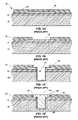
- FIGS. 1A-1Da conventional method of forming a through-wafer interconnect using spacer etching is shown.
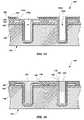
- FIG. 1Aillustrates a semiconductor device 10 having a substrate 12 (such as a silicon substrate) with a layer of borophosphosilicate glass 14 (BPSG) disposed on a surface thereof.
- BPSGborophosphosilicate glass 14
- a bond pad 16is formed over the layer of BPSG 14 , and a passivation layer 18 overlies the bond pad 16 .
- the passivation layer 18is etched, such as by reactive ion (dry) etching, so as to define an opening in the passivation layer 18 at a location above the bond pad 16 as shown in FIG. 1B .
- Another etching processis used to form a hole or an aperture 20 that extends into the silicon substrate 12 portion of the semiconductor device 10 as shown in FIG. 1C .
- a layer of insulative material 22(e.g., a pulsed deposition layer or “PDL”) is deposited over the passivation layer 18 , the bond pad 16 , and an inner surface of the aperture 20 .
- a conductive linermay also be coated over the passivation layer 18 , the bond pad 16 , and an inner surface of the aperture 20 .
- a spacer etching processmay also be used to remove portions of the layer of insulative material 22 , wherein portions of the layer of insulative material 22 are left on the inner surface of the aperture 20 and on the passivation layer 18 such as is illustrated in FIG. 1D .
- a conductive filler 24is disposed in the aperture and placed in contact with the bond pad 16 . The filler 24 is exposed through the back surface of the substrate to form the conductive via, as shown in FIG. 1D and as will be appreciated by those of ordinary skill in the art.
- the PDL filmwill form cracks on the surface due to a mismatch in the coefficient of thermal expansion (“CTE”) of the materials.
- CTEcoefficient of thermal expansion
- the present inventionin a number of embodiments, includes methods for forming through-wafer interconnects in semiconductor substrates and structures resulting from the methods.
- the disclosed methods of forming through-wafer interconnectsare more efficient, more economical and provide greater flexibility in the manufacturing and design of semiconductor devices in comparison to conventional methods of forming such structures.
- a method for forming a through-wafer interconnect in a substrateincludes providing a substrate having a pad on a surface of the substrate and depositing a passivation layer over the pad and the surface of the substrate. The method further includes forming an aperture through the passivation layer, the conductive pad and into the substrate using a substantially continuous process. A dielectric layer is disposed over the passivation layer and the inner surface of the aperture. The dielectric layer is removed from the passivation layer while leaving the dielectric layer on the inner surface of the aperture. The method also includes removing a portion of the passivation layer from the pad to expose a portion of the pad, filling the aperture with a conductive material and contacting the exposed portion of the pad with the conductive material.
- a semiconductor devicein another embodiment, includes a substrate having a first surface and an opposing, second surface, wherein the first surface has a pad with a passivation layer disposed thereon.
- An aperture having an inner surface coated with a dielectric layerextends through the conductive pad.
- the semiconductor devicealso includes a conductive layer overlying the dielectric layer, wherein a portion of the conductive layer protrudes from the aperture beyond a surface of the conductive pad.
- a method of forming a semiconductor deviceincludes providing a substrate having a first surface and a second, opposing surface and at least two conductive pads disposed on the first surface. At least two through-wafer interconnect (TWI) structures are formed including a first TWI structure formed through the first conductive pad and a second TWI structure formed through the second conductive pad. The first TWI structure and the first conductive pad are electrically connected while the second TWI structure is electrically insulated from the second conductive pad.
- TWIthrough-wafer interconnect
- the semiconductor deviceincludes a substrate having a first surface and a second, opposing surface, a first conductive pad disposed on the first surface and a second conductive pad disposed on the first surface.
- the semiconductor devicefurther includes a plurality of through-wafer interconnect (TWI) structures including a first TWI structure extending through and electrically connected with the first conductive pad and a second TWI structure extending through and electrically insulated from the second conductive pad.
- TWIthrough-wafer interconnect
- a method for forming a through-wafer interconnect in a substrateincludes providing a substrate having a pad on a surface of the substrate. The method further includes depositing a passivation layer over the pad and the surface of the substrate, and forming an aperture through the passivation layer and the pad. A dielectric layer is deposited over the passivation layer and an inner surface of the aperture. The method further includes removing a portion of the dielectric layer and a portion of the passivation layer, thus exposing a portion of the pad circumscribing the aperture, filling the aperture with a conductive material, and covering the exposed portion of the pad with the conductive material.
- the semiconductor deviceincludes a substrate having a first surface and an opposing, second surface, wherein the first surface has a pad and a passivation layer disposed thereon.
- An aperture having an inner surface coated with a dielectric layerextends through the pad.
- an uppermost surface of the dielectric layeris disposed below a lowermost surface of the pad.
- another method of forming a through-wafer interconnect in a substrateincludes providing a substrate having a pad on a surface of the substrate and depositing a passivation layer over the pad and the surface of the substrate. An aperture is formed through the passivation layer and the pad. The method also includes depositing a dielectric layer over the passivation layer and an inner surface of the aperture, and filling the aperture with a conductive material.
- Assemblies of stacked semiconductor devices including through-wafer interconnects according to the present inventionare also encompassed thereby.
- FIGS. 1A-1Dare cross-sectional views of a substrate illustrating acts of a conventional method of forming a through-wafer interconnect in a semiconductor device known in the art;
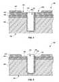
- FIG. 2is a cross-sectional view of a semiconductor device on which one embodiment of a method of forming a through-wafer interconnect is performed;
- FIG. 3is a cross-sectional view of the semiconductor device of FIG. 2 having an aperture formed therein;
- FIG. 4is a cross-sectional view of the semiconductor device of FIG. 3 having an insulative layer and a conductive liner formed in the aperture;
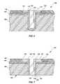
- FIG. 5is a cross-sectional view of the semiconductor device of FIG. 4 having a portion of the passivation layer removed to partially expose the bond pad;
- FIG. 6is a cross-sectional view of a through-wafer interconnect formed in the semiconductor device of FIG. 5 prior to exposing the interconnect through a backside surface of the substrate;
- FIG. 7is a cross-sectional view of a through-wafer interconnect with the interconnect structure being exposed through both surfaces of the semiconductor device;
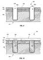
- FIG. 8depicts a cross-sectional view of a semiconductor device in which a through-wafer interconnect is formed in accordance with another embodiment of the present invention
- FIG. 9is a cross-sectional view of the semiconductor device of FIG. 8 having apertures formed therein;
- FIG. 10is a cross-sectional view of the semiconductor device of FIG. 9 having a resist plug, resist layer and mask formed thereon;
- FIG. 11illustrates a cross-sectional view of the semiconductor device of FIG. 10 with a portion of a pad exposed
- FIG. 12is a cross-sectional view of the semiconductor device of FIG. 11 after acts of the method of forming the through-wafer interconnects have been performed;
- FIG. 13is a cross-sectional view of the semiconductor device of FIG. 12 after additional acts of the methods of forming the through-wafer interconnects have been performed;
- FIG. 14is a cross-sectional view of a semiconductor device having two through-wafer interconnects formed therein prior to exposing the interconnect through a backside surface of the substrate;
- FIG. 15is a cross-sectional view of a through-wafer interconnect with the interconnect structure being exposed through both surfaces of the semiconductor device;
- FIG. 16Ais a schematic view of one embodiment of a PC board in a stacked arrangement with semiconductor devices having through-wafer interconnects produced with the methods of the present invention.
- FIGS. 16B and 16Care enlarged views of various portions of the stacked arrangement shown in FIG. 16A .
- the present inventionin a number of embodiments, includes methods for forming through-wafer interconnects that extend into a semiconductor substrate between a first surface of the semiconductor substrate and a second surface thereof, and the resulting structures.
- the present inventionmay be used to form so-called “through-wafer interconnects” (TWIs), which may also be referred to as vias, for electrically connecting integrated circuitry of a semiconductor device to integrated circuitry of another semiconductor device, to other electrical devices or in higher level packaging.
- TWIsthrough-wafer interconnects
- the TWI structures produced using the methods disclosed hereinmay be formed so as to be electrically connected to a bond pad or other metal structure to allow electrical connection to the integrated circuit and, in another embodiment, the TWI structures may be configured to pass through a bond pad without any electrical connection thereto.
- Semiconductor devices having the TWI structures produced using the methods disclosed hereinmay be used for example, for stacked die assemblies, chip select pads and the like.
- FIG. 2illustrates a cross-section of an exemplary semiconductor device 100 having a first surface 102 and an opposing, second surface 104 .
- the semiconductor device 100includes a semiconductor substrate 106 (e.g., a silicon substrate), a dielectric layer 108 (e.g., borophosphosilicate glass (BPSG)) and a passivation layer 120 .
- a conductive pad or line 122e.g., aluminum metal is disposed on the dielectric layer 108 .
- the conductive pad 122may be covered with the passivation layer 102 , for example, after the semiconductor has been subjected to one or more tests by contacting the conductive pad 122 of the semiconductor device 100 with a test probe as will be appreciated by those of ordinary skill in the art.
- the substrate 106may comprise, without limitation, a bulk semiconductor substrate (e.g., a full or partial wafer of a semiconductor material, such as silicon, gallium arsenide, indium phosphide, polysilicon, a silicon-on-insulator (SOI) type substrate, such as silicon-on-ceramic (SOC), silicon-on-glass (SOG), or silicon-on-sapphire (SOS), etc.), that may include a plurality of semiconductor devices thereof, and, optionally, semiconductor dice.
- a bulk semiconductor substratee.g., a full or partial wafer of a semiconductor material, such as silicon, gallium arsenide, indium phosphide, polysilicon
- SOIsilicon-on-insulator
- SOCsilicon-on-ceramic
- SOOGsilicon-on-glass
- SOSsilicon-on-sapphire
- the substrate 106may be a full thickness wafer as received from a vendor or a wafer that has been thinned (e.g., thereby defining the second surface 104 ), as by back grinding or wet etching, after fabrication of the integrated circuitry of the semiconductor device 100 ).
- the passivation layer 120may comprise a material other than BPSG, for example, a silicon oxide, silicon nitride, phosphosilicate glass (PSG), borosilicate glass (BSG), or another material, including one of a variety of insulative, organic (polymeric) materials which are available for passivation.
- the passivation materialmay be applied by chemical vapor deposition (CVD), plasma-enhanced chemical vapor deposition (PECVD), or other deposition method suitable for the type of passivation material used.
- the dielectric layer 108may also be formed from other dielectric materials such as, by way of example, silicon dioxide or silicon nitride.
- the semiconductor device 100may further include or be further processed to include other conductive elements, active areas or regions, transistors, capacitors, redistribution lines, or other structures comprising the integrated circuitry of semiconductor device 100 .
- the TWIs of the present inventionmay be formed at the semiconductor die level or at the wafer (or other bulk substrate) level, depending on the particular needs of the manufacturing process.
- FIGS. 2-8illustrate the fabrication of a single TWI in association with a single conductive pad 122
- the semiconductor device 100may be constructed to include multiple TWIs and that such TWIs may be associated with internal circuitry (not shown) or may be formed in “dead space” of the substrate 106 wherein no integrated circuitry resides.
- an aperture 124is formed as a blind hole in the semiconductor device 100 .
- the aperture 124is patterned and etched through the passivation layer 120 , the conductive pad 122 , the dielectric layer 108 (and any other materials that might be disposed above the substrate 106 ), and into the substrate 106 .
- the aperture 124may be formed by appropriately masking and patterning a photoresist or other material (e.g., oxide hard mask) and wet or dry etching to form the aperture 124 to a predetermined depth.
- the aperturemay be formed to a depth of approximately 200 ⁇ m.
- One suitable “wet” metal etchemploys a mixture of nitric acid and hydrofluoric (HF) acid in deionized (DI) water. “Dry” etching may also be termed reactive ion etching (RIE). Either a wet or dry etchant may be used to etch through the passivation layer 120 , the conductive pad 122 and the dielectric layer 108 to form the aperture 124 . In other embodiments, the aperture 124 may be formed by mechanical drilling, or use of an electromagnetic device such as a laser for laser ablation of the material of substrate 106 .
- an electromagnetic devicesuch as a laser for laser ablation of the material of substrate 106 .
- the aperture 124may subjected to a cleaning process to remove any unwanted reactants or impurities formed during the aperture formation process or, in the case of laser ablation, to remove heat-damaged portions of substrate 106 surrounding the aperture 124 and comprising a so-called “heat affected zone.”
- a cleaning solvent for such purposeis a 6% tetramethyl ammonium hydroxide (TMAH) in propylene glycol solution.
- an insulative layer 126is deposited on an inner surface of the aperture 124 and over the first surface 102 of the semiconductor device 100 .
- a conductive layer 128is subsequently disposed on the inner surface of the aperture 124 and the first surface 102 of the semiconductor device 100 .
- the insulative layer 126 and the conductive layer 128may be removed from the first surface 102 by chemical-mechanical polishing (CMP), as shown in FIG. 4 , in a manner such that the insulative layer 126 and the conductive layer 128 remain on the inner surfaces of the aperture 124 .
- CMPchemical-mechanical polishing
- CMPmay be used to remove the conductive layer 128 from the first surface 102 of the semiconductor device 100 while the insulative layer 126 is left in place on the first surface 102 of the semiconductor device 100 (not shown).
- the aperture 124may be filled with a polymer or a nickel (Ni) plate and solder in order to enable easier and more efficient CMP processing, and protection of the inner surface of the aperture 124 during the CMP process.
- the insulative layer 126may comprise a dielectric material such as, for example, a pulsed deposition layer (PDL), low silane oxide (LSO), ParyleneTM polymer such as that which is available from Specialty Coating Systems division of Cookson Electronics, silicon dioxide (SiO 2 ), aluminum oxide (Al 2 O 3 ), an organic polymeric material suitable for passivation purposes such as polybenzoxazole (PBO) or benzocyclobutene (BCB), or combinations of any thereof.
- PDLpulsed deposition layer
- LSOlow silane oxide
- ParyleneTM polymersuch as that which is available from Specialty Coating Systems division of Cookson Electronics
- silicon dioxideSiO 2
- Al 2 O 3aluminum oxide
- an organic polymeric material suitable for passivation purposessuch as polybenzoxazole (PBO) or benzocyclobutene (BCB), or combinations of any thereof.
- insulative layer 126Other dielectric materials that may be used as the insulative layer 126 include tetraethyl orthosilicate (TEOS), spin-on glass, thermal oxide, a pulse deposition layer comprising aluminum rich oxide, silicon nitride, silicon oxynitride, a glass (i.e., borophosphosilicate glass (BPSG), phosphosilicate glass, borosilicate glass), or any other suitable dielectric material known in the art.
- TEOStetraethyl orthosilicate
- spin-on glassthermal oxide
- a pulse deposition layercomprising aluminum rich oxide, silicon nitride, silicon oxynitride, a glass (i.e., borophosphosilicate glass (BPSG), phosphosilicate glass, borosilicate glass), or any other suitable dielectric material known in the art.
- BPSGborophosphosilicate glass
- phosphosilicate glassborosilicate glass
- the conductive layer 128may include another layer such as a plating-attractive coating (PAC) or some type of seed layer that is placed over the insulation layer 126 to enhance the deposition of the conductive layer 128 .
- PACplating-attractive coating
- TiNtitanium nitride
- CVDchemical vapor deposition
- conductive materialsthat may be used to form the conductive layer 128 include, without limitation, titanium (Ti), polysilicon (Si), palladium (Pd), tin (Sn), tantalum (Ta), tungsten (W), cobalt (Co), copper (Cu), silver (Ag), aluminum (Al), iridium (Ir), gold (Au), molybdenum (Mo), platinum (Pt), nickel-phosphorus (NiP), palladium-phosphorus (Pd—P), cobalt-phosphorus (Co—P), a cobalt-tungsten-phosphorous (Co—W—P) alloy, other alloys of any of the foregoing metals, a conductive polymer or conductive material entrained in a polymer (i.e., conductive or conductor-filled epoxy) and mixtures of any thereof.
- deposition processesthat may be used to deposit the various layers of the conductive layer 128 include metalloorganic chemical vapor deposition (MOCVD), physical vapor deposition (PVD), plasma-enhanced chemical vapor deposition (PECVD), vacuum evaporation and sputtering.
- MOCVDmetalloorganic chemical vapor deposition
- PVDphysical vapor deposition
- PECVDplasma-enhanced chemical vapor deposition
- vacuum evaporation and sputteringvacuum evaporation and sputtering.
- a portion of the passivation layer 120 overlying the conductive pad 122is removed such as by using a conventional photolithographic patterning and etching process to form an opening over and at least partially expose the conductive pad 122 .
- a mask 129FIG. 4
- a suitable etchantmay be used to remove the portion of the passivation layer 120 exposed through an aperture 129 a in the mask 129 and form an opening above the conductive pad 122 .
- a portion of the insulative layer 126 contacting the conductive layer 128 and above the conductive pad 122may or may not be removed depending on the type of etchant used. As illustrated in FIG. 5 , the portion of the insulative layer 126 above the conductive pad 122 has been removed to enable easier connection of the conductive pad 122 to the resulting TWI. In another embodiment, the portion of the conductive layer 128 protruding above the conductive pad 122 may be removed such as, for example, with CMP.
- the conductive layer 128may be used to protect the insulative layer 126 during an etching process, the conductive layer 128 may also be applied over the conductive pad 122 and the insulative layer 126 after the conductive pad 122 has been exposed (i.e., after the acts described with reference to FIG. 5 ).
- a metal layer 130is deposited on the conductive pad 122 , the inner surface of the aperture 124 (i.e., the inner surface of the conductive layer 128 ), and the external surface of the portion of the conductive layer 128 protruding above the conductive pad 122 .
- the metal layer 130may include a nickel and may be deposited by electroless or electrolytic plating.
- the metal layer 130 of nickelmay be coated with a further copper layer.
- the metal layer 130may comprise tantalum or copper, and may be deposited by physical vapor deposition (PVD).
- the remaining portion of the aperture and the defined openings above the conductive pad 122are filled with a conductive material 132 such as, for example, solder.
- a conductive material 132such as, for example, solder.
- the soldermay be applied with a wave solder process.
- the aperture and the volume above the conductive pad 122may be filled with other conductive materials 132 which may comprise a metal, metal powder, a metal or alloy powder, a flowable conductive photopolymer, a thermoplastic conductive resin, resin-covered particulate metal material, or other suitable material which may be used to form a solid, conductive TWI.
- CMPconventional back grinding or another known mechanical or chemical process may be used to complete the TWI structure by exposing the conductive material 132 through the second surface 104 of the substrate 106 for subsequent connection to, for example, circuitry of an external component.
- the resulting TWI structureis connected to the conductive pad 122 by way of the conductive material 132 and the conductive layer 128 .
- FIG. 8illustrates a cross-section of an exemplary semiconductor device 140 having a first surface 142 and an opposing, second surface 144 .
- the semiconductor device 140includes a substrate 146 (e.g., a silicon substrate), a dielectric layer 148 (e.g., BPSG), and a passivation layer 150 .
- Two conductive pads 152 a and 152 bare disposed on the dielectric layer 148 .
- the conductive pads 152 a and 152 bare covered by the passivation layer 150 after the semiconductor device 140 has been subjected to one or more tests by contacting and the pads 152 a and 152 b are contacted with test probes.
- the substrate 146may comprise, without limitation, a bulk semiconductor substrate (e.g., a full or partial wafer of a semiconductor material, such as silicon, gallium arsenide, indium phosphide, polysilicon, a silicon-on-insulator (SOI) type substrate, such as silicon-on-ceramic (SOC), silicon-on-glass (SOG), or silicon-on-sapphire (SOS), etc.) that may include a plurality of semiconductor devices thereof, and, optionally, semiconductor dice.
- a bulk semiconductor substratee.g., a full or partial wafer of a semiconductor material, such as silicon, gallium arsenide, indium phosphide, polysilicon
- SOIsilicon-on-insulator
- SOCsilicon-on-ceramic
- SOOGsilicon-on-glass
- SOSsilicon-on-sapphire
- the substrate 146may also be a full thickness wafer as received from a vendor or a wafer that has been thinned (e.g., thereby defining the second surface 144 ) after fabrication of the semiconductor device 140 ).
- the dielectric layer 148may be formed from materials such as, by way of example, silicon dioxide or silicon nitride. Although not illustrated, it will be appreciated by those of ordinary skill in the art that the semiconductor device 140 may include or be further processed to include other conductive elements, active areas or regions, transistors, capacitors, redistribution lines, or other structures used to produce integrated circuitry.
- pad 152 ais to be ultimately electrically connected to the TWI that is to be formed in association therewith while pad 152 b is not to be electrically connected to the TWI that is to be formed in association with pad 152 B.
- pad 152 ait may be desirable to have a TWI that passes through one of the stacked chips without electrically connecting to a bond pad of the chip.
- the semiconductor device 140may be configured with any number of TWIs which are either electrically connected to a conductive pad (i.e., as with conductive pad 152 a ) or not electrically connected to conductive pads (i.e., as with conductive pad 152 b ) as well as various combinations thereof.
- FIG. 9illustrates the semiconductor device 140 having apertures 154 a and 154 b formed therein.
- the apertures 154 a and 154 bmay be formed by patterning and etching through the passivation layer 150 , the pads 152 a and 152 b, the dielectric layer 148 (and any other materials disposed over the substrate 146 ), and into the substrate 146 .
- the apertures 154 a and 154 bmay be formed by appropriately masking and patterning a photoresist or other material (e.g., hard oxide mask) and wet or dry etching to form the apertures 154 a and 154 b to a desired depth such as, for example, about 200 ⁇ m.
- a photoresist or other materiale.g., hard oxide mask
- wet or dry etchinge.g., hard oxide mask
- One suitable “wet” metal etchemploys a mixture of nitric acid and hydrofluoric (HF) acid in deionized
- the apertures 154 a and 154 bmay be formed by mechanical drilling, or use of an electromagnetic device such as a laser for laser ablation. After formation, the apertures 154 a and 154 b may further be subjected to a cleaning process to remove any unwanted reactants, impurities or damaged substrate material resulting from the aperture formation process.
- any mask used to pattern and etch the apertures 154 a and 154 bis stripped away and a dielectric layer 156 is deposited on the inner surfaces of the apertures 154 a and 154 b and over the passivation layer 150 .
- the dielectric layer 156may comprise a dielectric material such as, for example, LSO, ParyleneTM, silicon dioxide (SiO 2 ), aluminum oxide (Al 2 O 3 ), TEOS, or combinations of any and may be deposited using known techniques.
- the apertures 154 a and 154 bare filled with a resist plug 158 such as, for example, by disposing a polymer resist in the apertures 154 a and 154 b and curing the polymer.
- a mask 159is then patterned on the structure.
- an opening(such as, for example, an annular opening as illustrated is defined over the conductive pad 152 a to expose the conductive pad 152 a such as by patterning with the mask 159 and etching with a selective etchant that is capable of etching away or removing the dielectric layer 156 and the passivation layer 150 overlying the conductive pad 152 a such as is shown in FIG. 11 .
- the selective etchantexposes a portion of the conductive pad 152 a and also removes a portion of the dielectric layer 156 circumscribing the resist plug 158 , such that an uppermost surface of the dielectric layer 156 disposed in the aperture 154 a is slightly recessed below a lowermost surface of the conductive pad 152 a.
- the mask 159is then stripped away, resulting in the semiconductor device 140 shown in FIG. 12 .
- Such a processenables a later deposited conductive layer to electrically connect the conductive pad 152 a to a conductive material deposited in the aperture 154 a.
- the acts of opening the pad 152 a and aperture 154 a formationmay be reversed in sequence, wherein defining the opening above the conductive pad 152 a occurs first, followed by the formation of the aperture 154 a.
- the resist plugs 158are removed by appropriate stripping and a seed layer 160 is deposited over exposed surfaces of the semiconductor device 140 .
- the seed layer 160is deposited with atomic layer deposition (ALD) techniques to form a layer of tungsten (W) as the seed layer 160 .
- the seed layer 160may comprise tantalum (Ta) or copper (Cu) and be deposited with physical vapor deposition (PVD) techniques, or the seed layer 160 may comprise copper (Cu) or nickel (Ni) and be deposited with electroplating.
- a solder wettable material layer 162may be deposited over the seed layer 160 with an electroless or electroplating method.
- the solder wettable material layer 162may comprise nickel (Ni) or other solder-wettable metals.
- a conductive material 164such as, for example, solder is deposited over the solder wettable material layer 162 by plating, dipping the semiconductor device 140 in molten solder or other known conductive material deposition technique.
- the conductive material 164adheres to the majority of the exposed surfaces of the solder wettable material layer 162 and, thus, after deposition of the conductive material 164 , an abrasive technique such as CMP or another appropriate process may be used to remove the conductive material 164 , the solder wettable material layer 162 , and the seed layer 160 extending laterally between the two TWIs to prevent the various conductive materials of one TWI to be connected with those of another TWI and, therefore, preventing any shorting therebetween.
- CMPabrasive technique
- the CMP processmay further be used to remove the dielectric layer 156 and expose the passivation layer 150 as a flat, controlled surface.
- other conductive materialsmay be used to fill the apertures 154 a and 154 b to produce a conductive pathway in the TWIs.
- PVDphysical vapor deposition
- a solder pastemay also be placed in the apertures 154 a and 154 b and reflowed. Further, a conductive or conductor-filled epoxy may be used.
- an abrasive processsuch as CMP may be performed to remove the solder wettable material layer 162 and the seed layer 160 from the passivation layer 150 before the conductive material 164 is deposited.
- a CMP processwill again be used to remove any excess conductive material 164 in order to expose the passivation layer 150 as a flat, controlled surface.
- the TWI structures 166 a and 166 bare completed with the thinning of the substrate, such as by CMP, conventional back grinding or another appropriate process to expose the conductive material 164 through the second surface 144 of the semiconductor device 140 .
- the methods describedmay be used to form a TWI structure 166 a that is connected to an adjacent conductive pad 152 a as well as a TWI structure 166 b that is not electrically connected to an adjacent conductive pad 152 b.
- the TWI structure 166 b adjacent the conductive pad 152 b that is not electrically connected to the conductive material 164goes through substantially the same acts as the TWI structure 166 a having the conductive pad 152 a that is electrically connected to the conductive material 164 .
- an openingis not defined over the conductive pad 152 b.
- the insulative layer 156remains between and electrically isolates the conductive pad 152 b from and the conductive layers 160 and 162 and the conductive material 164 as illustrated in FIGS. 13-15 .
- the semiconductor devices 140may further be configured with a redistribution layer comprising traces and, optionally, associated discrete external conductive elements thereon such as solder bumps which may be formed on either or both of the surfaces 142 or 144 and electrically interconnected with the TWI structures 166 a and 166 b, as will be appreciated by those or ordinary skill in the art.
- a redistribution layercomprising traces and, optionally, associated discrete external conductive elements thereon such as solder bumps which may be formed on either or both of the surfaces 142 or 144 and electrically interconnected with the TWI structures 166 a and 166 b, as will be appreciated by those or ordinary skill in the art.
- FIG. 16Aillustrates one embodiment of a higher level packaging system including TWIs produced with one or more of the methods of the instant invention.
- a PC board 170 having a first semiconductor device 140 and a second semiconductor device 140 ′ in a stacked arrangementis depicted.
- the first semiconductor device 140may be configured with TWI structures 166 a - 166 d and the second semiconductor device 140 ′ may be configured with TWI structures 166 e - 166 h.
- Use of such TWI structures 166 a - 166 hprovides substantial flexibility in designing and fabricating semiconductor devices and related assemblies.
- TWI structure 166 f of the second semiconductor device 140 ′is electrically coupled with TWI structure 166 b of the first semiconductor device 140 (such as by a conductive bump, solder ball, or other appropriate structure).
- TWI structure 166 bis not electrically coupled to the bond pad (or line) 152 b. Referring to FIG.
- the assemblyalso includes a TWI structure 166 g (of the second semiconductor device 140 ′) that is not connected to an adjacent TWI structure 166 c (of the second semiconductor device 140 ′).
- TWI structure 166 cis, however, coupled with its associated bond pad (or line) 152 c.
- a TWI structureis connected to an associated bond pad (or line) and an adjacent TWI structure (e.g., the arrangement represented by TWI structure 166 a, bond pad 152 a and TWI structure 166 e ); or wherein a TWI structure is not coupled to either of an associated bond pad (or line) or an adjacent TWI structure (e.g., the arrangement represented by TWI structure 166 d, bond pad 152 d and TWI structure 166 h ).
Landscapes
- Engineering & Computer Science (AREA)
- Microelectronics & Electronic Packaging (AREA)
- Physics & Mathematics (AREA)
- Condensed Matter Physics & Semiconductors (AREA)
- General Physics & Mathematics (AREA)
- Computer Hardware Design (AREA)
- Power Engineering (AREA)
- Manufacturing & Machinery (AREA)
- Internal Circuitry In Semiconductor Integrated Circuit Devices (AREA)
Abstract
Description
- This application is a divisional of application Ser. No. 11/219,132, filed Sep. 1, 2005, pending. Also, this application is related to application Ser. No. 11/138,544, filed May 26, 2005, now U.S. Pat. No. 7,109,068, issued Sep. 19, 2006; application Ser. No. 11/384,069, filed Mar. 17, 2006, pending; application Ser. No. 11/198,338, filed Aug. 5, 2005, now U.S. Pat. No. 7,429,529, issued Sep. 30, 2008; and application Ser. No. 12/186,913, filed Aug. 6, 2008, pending.
- 1. Field of the Invention
- The present invention relates generally to semiconductor manufacturing techniques and methods of forming electrical contacts in semiconductor substrates. More particularly, the present invention relates to methods of forming through-wafer interconnects in semiconductor substrates and structures resulting therefrom.
- 2. State of the Art
- Semiconductor substrates often have vias extending therethrough, wherein the vias are filled with conductive materials to form interconnects (commonly known as a through-wafer interconnect, or “TWI”) used, for example, to connect circuitry on one surface of the semiconductor device to circuitry on another surface thereof, or to accommodate connection with external circuitry.
- As used herein, a “via” refers to a hole or aperture having conductive material or a conductive member therein and which extends substantially through a substrate (e.g., from one surface substantially to another opposing surface). The via may be used accommodate electrical connection of a semiconductor device, an electrical component, or circuitry located on side of the substrate other than where bond pads have been formed. Vias are conventionally formed in a variety of substrates for a variety of uses. For example, interposers for single die packages, interconnects for multi-die packages, and contact probe cards for temporarily connecting semiconductor dice to a test apparatus often employ vias in their structures.
- One known method of forming through-wafer interconnect structures includes a process known as spacer etching. Spacer etching is a relatively complicated and costly procedure. Referring to
FIGS. 1A-1D a conventional method of forming a through-wafer interconnect using spacer etching is shown.FIG. 1A illustrates asemiconductor device 10 having a substrate12 (such as a silicon substrate) with a layer of borophosphosilicate glass14 (BPSG) disposed on a surface thereof. Abond pad 16 is formed over the layer ofBPSG 14, and apassivation layer 18 overlies thebond pad 16. Thepassivation layer 18 is etched, such as by reactive ion (dry) etching, so as to define an opening in thepassivation layer 18 at a location above thebond pad 16 as shown inFIG. 1B . Another etching process is used to form a hole or anaperture 20 that extends into thesilicon substrate 12 portion of thesemiconductor device 10 as shown inFIG. 1C . - As also depicted in
FIG. 1C , a layer of insulative material22 (e.g., a pulsed deposition layer or “PDL”) is deposited over thepassivation layer 18, thebond pad 16, and an inner surface of theaperture 20. Optionally, a conductive liner may also be coated over thepassivation layer 18, thebond pad 16, and an inner surface of theaperture 20. By forming the through-wafer interconnect in this manner, the layer ofinsulative material 22 is deposited on the exposed portion ofbond pad 16 and must be subsequently removed. A spacer etching process may also be used to remove portions of the layer ofinsulative material 22, wherein portions of the layer ofinsulative material 22 are left on the inner surface of theaperture 20 and on thepassivation layer 18 such as is illustrated inFIG. 1D . Aconductive filler 24 is disposed in the aperture and placed in contact with thebond pad 16. Thefiller 24 is exposed through the back surface of the substrate to form the conductive via, as shown inFIG. 1D and as will be appreciated by those of ordinary skill in the art. - Under some conditions, e.g., the use of polyimide as a passivation layer, the PDL film will form cracks on the surface due to a mismatch in the coefficient of thermal expansion (“CTE”) of the materials. The subsequently performed spacer etch will replicate those cracks into the passivation layer ultimately causing shorting when metal is used to coat the sidewalls of the via.
- It is a continuing desire to improve the manufacturing techniques and processes used in semiconductor fabrication including those associated with forming TWI structures. It would be advantageous to provide methods of forming through-wafer interconnect structures having improved efficiency and which are more cost effective than conventional techniques such as those which employ conventional spacer etching techniques.
- The present invention, in a number of embodiments, includes methods for forming through-wafer interconnects in semiconductor substrates and structures resulting from the methods. The disclosed methods of forming through-wafer interconnects are more efficient, more economical and provide greater flexibility in the manufacturing and design of semiconductor devices in comparison to conventional methods of forming such structures.
- In accordance with one embodiment of the present invention, a method for forming a through-wafer interconnect in a substrate includes providing a substrate having a pad on a surface of the substrate and depositing a passivation layer over the pad and the surface of the substrate. The method further includes forming an aperture through the passivation layer, the conductive pad and into the substrate using a substantially continuous process. A dielectric layer is disposed over the passivation layer and the inner surface of the aperture. The dielectric layer is removed from the passivation layer while leaving the dielectric layer on the inner surface of the aperture. The method also includes removing a portion of the passivation layer from the pad to expose a portion of the pad, filling the aperture with a conductive material and contacting the exposed portion of the pad with the conductive material.
- In another embodiment, a semiconductor device is described. The semiconductor device includes a substrate having a first surface and an opposing, second surface, wherein the first surface has a pad with a passivation layer disposed thereon. An aperture having an inner surface coated with a dielectric layer extends through the conductive pad. The semiconductor device also includes a conductive layer overlying the dielectric layer, wherein a portion of the conductive layer protrudes from the aperture beyond a surface of the conductive pad.
- In yet another embodiment of the present invention, a method of forming a semiconductor device includes providing a substrate having a first surface and a second, opposing surface and at least two conductive pads disposed on the first surface. At least two through-wafer interconnect (TWI) structures are formed including a first TWI structure formed through the first conductive pad and a second TWI structure formed through the second conductive pad. The first TWI structure and the first conductive pad are electrically connected while the second TWI structure is electrically insulated from the second conductive pad.
- In accordance with another aspect of the present invention, another semiconductor device is provided. The semiconductor device includes a substrate having a first surface and a second, opposing surface, a first conductive pad disposed on the first surface and a second conductive pad disposed on the first surface. The semiconductor device further includes a plurality of through-wafer interconnect (TWI) structures including a first TWI structure extending through and electrically connected with the first conductive pad and a second TWI structure extending through and electrically insulated from the second conductive pad.
- In yet a further embodiment, a method for forming a through-wafer interconnect in a substrate includes providing a substrate having a pad on a surface of the substrate. The method further includes depositing a passivation layer over the pad and the surface of the substrate, and forming an aperture through the passivation layer and the pad. A dielectric layer is deposited over the passivation layer and an inner surface of the aperture. The method further includes removing a portion of the dielectric layer and a portion of the passivation layer, thus exposing a portion of the pad circumscribing the aperture, filling the aperture with a conductive material, and covering the exposed portion of the pad with the conductive material.
- Another semiconductor device is disclosed in an additional embodiment. The semiconductor device includes a substrate having a first surface and an opposing, second surface, wherein the first surface has a pad and a passivation layer disposed thereon. An aperture having an inner surface coated with a dielectric layer extends through the pad. In the semiconductor device, an uppermost surface of the dielectric layer is disposed below a lowermost surface of the pad.
- In yet a further embodiment, another method of forming a through-wafer interconnect in a substrate includes providing a substrate having a pad on a surface of the substrate and depositing a passivation layer over the pad and the surface of the substrate. An aperture is formed through the passivation layer and the pad. The method also includes depositing a dielectric layer over the passivation layer and an inner surface of the aperture, and filling the aperture with a conductive material.
- Assemblies of stacked semiconductor devices including through-wafer interconnects according to the present invention are also encompassed thereby.
- In the drawings, which depict exemplary embodiments of various features of the present invention, and in which various elements are not necessarily to scale:
FIGS. 1A-1D are cross-sectional views of a substrate illustrating acts of a conventional method of forming a through-wafer interconnect in a semiconductor device known in the art;FIG. 2 is a cross-sectional view of a semiconductor device on which one embodiment of a method of forming a through-wafer interconnect is performed;FIG. 3 is a cross-sectional view of the semiconductor device ofFIG. 2 having an aperture formed therein;FIG. 4 is a cross-sectional view of the semiconductor device ofFIG. 3 having an insulative layer and a conductive liner formed in the aperture;FIG. 5 is a cross-sectional view of the semiconductor device ofFIG. 4 having a portion of the passivation layer removed to partially expose the bond pad;FIG. 6 is a cross-sectional view of a through-wafer interconnect formed in the semiconductor device ofFIG. 5 prior to exposing the interconnect through a backside surface of the substrate;FIG. 7 is a cross-sectional view of a through-wafer interconnect with the interconnect structure being exposed through both surfaces of the semiconductor device;FIG. 8 depicts a cross-sectional view of a semiconductor device in which a through-wafer interconnect is formed in accordance with another embodiment of the present invention;FIG. 9 is a cross-sectional view of the semiconductor device ofFIG. 8 having apertures formed therein;FIG. 10 is a cross-sectional view of the semiconductor device ofFIG. 9 having a resist plug, resist layer and mask formed thereon;FIG. 11 illustrates a cross-sectional view of the semiconductor device ofFIG. 10 with a portion of a pad exposed;FIG. 12 is a cross-sectional view of the semiconductor device ofFIG. 11 after acts of the method of forming the through-wafer interconnects have been performed;FIG. 13 is a cross-sectional view of the semiconductor device ofFIG. 12 after additional acts of the methods of forming the through-wafer interconnects have been performed;FIG. 14 is a cross-sectional view of a semiconductor device having two through-wafer interconnects formed therein prior to exposing the interconnect through a backside surface of the substrate;FIG. 15 is a cross-sectional view of a through-wafer interconnect with the interconnect structure being exposed through both surfaces of the semiconductor device;FIG. 16A is a schematic view of one embodiment of a PC board in a stacked arrangement with semiconductor devices having through-wafer interconnects produced with the methods of the present invention; andFIGS. 16B and 16C are enlarged views of various portions of the stacked arrangement shown inFIG. 16A .- The present invention, in a number of embodiments, includes methods for forming through-wafer interconnects that extend into a semiconductor substrate between a first surface of the semiconductor substrate and a second surface thereof, and the resulting structures. The present invention may be used to form so-called “through-wafer interconnects” (TWIs), which may also be referred to as vias, for electrically connecting integrated circuitry of a semiconductor device to integrated circuitry of another semiconductor device, to other electrical devices or in higher level packaging. For instance, in one embodiment, the TWI structures produced using the methods disclosed herein may be formed so as to be electrically connected to a bond pad or other metal structure to allow electrical connection to the integrated circuit and, in another embodiment, the TWI structures may be configured to pass through a bond pad without any electrical connection thereto. Semiconductor devices having the TWI structures produced using the methods disclosed herein may be used for example, for stacked die assemblies, chip select pads and the like.
- Referring to
FIGS. 2-7 , acts in one method of the present invention for forming through-wafer interconnects (TWIs) are disclosed.FIG. 2 illustrates a cross-section of anexemplary semiconductor device 100 having afirst surface 102 and an opposing,second surface 104. Thesemiconductor device 100 includes a semiconductor substrate106 (e.g., a silicon substrate), a dielectric layer108 (e.g., borophosphosilicate glass (BPSG)) and apassivation layer 120. A conductive pad or line122 (e.g., aluminum metal) is disposed on thedielectric layer 108. In one embodiment, theconductive pad 122 may be covered with thepassivation layer 102, for example, after the semiconductor has been subjected to one or more tests by contacting theconductive pad 122 of thesemiconductor device 100 with a test probe as will be appreciated by those of ordinary skill in the art. - The
substrate 106 may comprise, without limitation, a bulk semiconductor substrate (e.g., a full or partial wafer of a semiconductor material, such as silicon, gallium arsenide, indium phosphide, polysilicon, a silicon-on-insulator (SOI) type substrate, such as silicon-on-ceramic (SOC), silicon-on-glass (SOG), or silicon-on-sapphire (SOS), etc.), that may include a plurality of semiconductor devices thereof, and, optionally, semiconductor dice. If thesubstrate 106 is a wafer, thesubstrate 106 may be a full thickness wafer as received from a vendor or a wafer that has been thinned (e.g., thereby defining the second surface104), as by back grinding or wet etching, after fabrication of the integrated circuitry of the semiconductor device100). - The
passivation layer 120 may comprise a material other than BPSG, for example, a silicon oxide, silicon nitride, phosphosilicate glass (PSG), borosilicate glass (BSG), or another material, including one of a variety of insulative, organic (polymeric) materials which are available for passivation. The passivation material may be applied by chemical vapor deposition (CVD), plasma-enhanced chemical vapor deposition (PECVD), or other deposition method suitable for the type of passivation material used. Thedielectric layer 108 may also be formed from other dielectric materials such as, by way of example, silicon dioxide or silicon nitride. Although not illustrated, it will appreciated by those of ordinary skill in the art that thesemiconductor device 100 may further include or be further processed to include other conductive elements, active areas or regions, transistors, capacitors, redistribution lines, or other structures comprising the integrated circuitry ofsemiconductor device 100. - The TWIs of the present invention may be formed at the semiconductor die level or at the wafer (or other bulk substrate) level, depending on the particular needs of the manufacturing process. Thus, while
FIGS. 2-8 illustrate the fabrication of a single TWI in association with a singleconductive pad 122, it should be understood that thesemiconductor device 100 may be constructed to include multiple TWIs and that such TWIs may be associated with internal circuitry (not shown) or may be formed in “dead space” of thesubstrate 106 wherein no integrated circuitry resides. - Referring now to
FIG. 3 , anaperture 124 is formed as a blind hole in thesemiconductor device 100. In one embodiment, theaperture 124 is patterned and etched through thepassivation layer 120, theconductive pad 122, the dielectric layer108 (and any other materials that might be disposed above the substrate106), and into thesubstrate 106. Theaperture 124 may be formed by appropriately masking and patterning a photoresist or other material (e.g., oxide hard mask) and wet or dry etching to form theaperture 124 to a predetermined depth. For example, in one embodiment, the aperture may be formed to a depth of approximately 200 μm. - One suitable “wet” metal etch employs a mixture of nitric acid and hydrofluoric (HF) acid in deionized (DI) water. “Dry” etching may also be termed reactive ion etching (RIE). Either a wet or dry etchant may be used to etch through the
passivation layer 120, theconductive pad 122 and thedielectric layer 108 to form theaperture 124. In other embodiments, theaperture 124 may be formed by mechanical drilling, or use of an electromagnetic device such as a laser for laser ablation of the material ofsubstrate 106. After formation, theaperture 124 may subjected to a cleaning process to remove any unwanted reactants or impurities formed during the aperture formation process or, in the case of laser ablation, to remove heat-damaged portions ofsubstrate 106 surrounding theaperture 124 and comprising a so-called “heat affected zone.” One suitable cleaning solvent for such purpose is a 6% tetramethyl ammonium hydroxide (TMAH) in propylene glycol solution. - Referring now to
FIG. 4 , aninsulative layer 126 is deposited on an inner surface of theaperture 124 and over thefirst surface 102 of thesemiconductor device 100. Aconductive layer 128 is subsequently disposed on the inner surface of theaperture 124 and thefirst surface 102 of thesemiconductor device 100. Theinsulative layer 126 and theconductive layer 128 may be removed from thefirst surface 102 by chemical-mechanical polishing (CMP), as shown inFIG. 4 , in a manner such that theinsulative layer 126 and theconductive layer 128 remain on the inner surfaces of theaperture 124. In another embodiment, CMP may be used to remove theconductive layer 128 from thefirst surface 102 of thesemiconductor device 100 while theinsulative layer 126 is left in place on thefirst surface 102 of the semiconductor device100 (not shown). In yet an additional embodiment, theaperture 124 may be filled with a polymer or a nickel (Ni) plate and solder in order to enable easier and more efficient CMP processing, and protection of the inner surface of theaperture 124 during the CMP process. - The
insulative layer 126 may comprise a dielectric material such as, for example, a pulsed deposition layer (PDL), low silane oxide (LSO), Parylene™ polymer such as that which is available from Specialty Coating Systems division of Cookson Electronics, silicon dioxide (SiO2), aluminum oxide (Al2O3), an organic polymeric material suitable for passivation purposes such as polybenzoxazole (PBO) or benzocyclobutene (BCB), or combinations of any thereof. Other dielectric materials that may be used as theinsulative layer 126 include tetraethyl orthosilicate (TEOS), spin-on glass, thermal oxide, a pulse deposition layer comprising aluminum rich oxide, silicon nitride, silicon oxynitride, a glass (i.e., borophosphosilicate glass (BPSG), phosphosilicate glass, borosilicate glass), or any other suitable dielectric material known in the art. Methods of depositing theinsulative layer 126 are known by those of ordinary skill in the art and may vary depending on the type of material used for theinsulative layer 126. - In one embodiment, the
conductive layer 128 may include another layer such as a plating-attractive coating (PAC) or some type of seed layer that is placed over theinsulation layer 126 to enhance the deposition of theconductive layer 128. For instance, titanium nitride (TiN) may be placed over theinsulation layer 126 using chemical vapor deposition (CVD) techniques to act as the PAC for the subsequent deposition of the seed layer with a plating process such as, for example, electroless or electrolytic plating to form theconductive layer 128. - Other conductive materials that may be used to form the
conductive layer 128 include, without limitation, titanium (Ti), polysilicon (Si), palladium (Pd), tin (Sn), tantalum (Ta), tungsten (W), cobalt (Co), copper (Cu), silver (Ag), aluminum (Al), iridium (Ir), gold (Au), molybdenum (Mo), platinum (Pt), nickel-phosphorus (NiP), palladium-phosphorus (Pd—P), cobalt-phosphorus (Co—P), a cobalt-tungsten-phosphorous (Co—W—P) alloy, other alloys of any of the foregoing metals, a conductive polymer or conductive material entrained in a polymer (i.e., conductive or conductor-filled epoxy) and mixtures of any thereof. - Other deposition processes that may be used to deposit the various layers of the
conductive layer 128 include metalloorganic chemical vapor deposition (MOCVD), physical vapor deposition (PVD), plasma-enhanced chemical vapor deposition (PECVD), vacuum evaporation and sputtering. It will be appreciated by those of ordinary skill in the art that the type and thickness of material of the various layers or materials used for theconductive layer 128 and the deposition processes used to deposit the layers of theconductive layer 128 will vary depending on, for example, the electrical requirements and the type of desired material used to form the TWI and the intended use of the TWI. - Referring now to
FIG. 5 , a portion of thepassivation layer 120 overlying theconductive pad 122 is removed such as by using a conventional photolithographic patterning and etching process to form an opening over and at least partially expose theconductive pad 122. For instance, a mask129 (FIG. 4 ) of a photoresist material may be disposed, patterned and developed on thepassivation layer 120 and a suitable etchant may be used to remove the portion of thepassivation layer 120 exposed through anaperture 129ain themask 129 and form an opening above theconductive pad 122. Further, a portion of theinsulative layer 126 contacting theconductive layer 128 and above theconductive pad 122 may or may not be removed depending on the type of etchant used. As illustrated inFIG. 5 , the portion of theinsulative layer 126 above theconductive pad 122 has been removed to enable easier connection of theconductive pad 122 to the resulting TWI. In another embodiment, the portion of theconductive layer 128 protruding above theconductive pad 122 may be removed such as, for example, with CMP. In another embodiment, since theconductive layer 128 may be used to protect theinsulative layer 126 during an etching process, theconductive layer 128 may also be applied over theconductive pad 122 and theinsulative layer 126 after theconductive pad 122 has been exposed (i.e., after the acts described with reference toFIG. 5 ). - Turning now to
FIG. 6 , ametal layer 130 is deposited on theconductive pad 122, the inner surface of the aperture124 (i.e., the inner surface of the conductive layer128), and the external surface of the portion of theconductive layer 128 protruding above theconductive pad 122. In one embodiment, themetal layer 130 may include a nickel and may be deposited by electroless or electrolytic plating. In another embodiment, themetal layer 130 of nickel may be coated with a further copper layer. In other embodiments, themetal layer 130 may comprise tantalum or copper, and may be deposited by physical vapor deposition (PVD). - After deposition of the
metal layer 130, the remaining portion of the aperture and the defined openings above theconductive pad 122 are filled with aconductive material 132 such as, for example, solder. In one embodiment, the solder may be applied with a wave solder process. In other embodiments, the aperture and the volume above theconductive pad 122 may be filled with otherconductive materials 132 which may comprise a metal, metal powder, a metal or alloy powder, a flowable conductive photopolymer, a thermoplastic conductive resin, resin-covered particulate metal material, or other suitable material which may be used to form a solid, conductive TWI. - As shown in
FIG. 7 , CMP, conventional back grinding or another known mechanical or chemical process may be used to complete the TWI structure by exposing theconductive material 132 through thesecond surface 104 of thesubstrate 106 for subsequent connection to, for example, circuitry of an external component. The resulting TWI structure is connected to theconductive pad 122 by way of theconductive material 132 and theconductive layer 128. - It is noted that, by using the process of the presently described embodiment, only two etch procedures using a mask are employed; once to form the
aperture 124 described with respect toFIG. 3 and then again to define the opening above theconductive pad 122 as seen inFIG. 5 . The prior art process described herein with reference toFIGS. 1A-1D uses an etching process three different times. For instance, etching is used to open thebond pad 16, again to form theaperture 20, and spacer etching is finally used to remove the layer ofinsulative material 22 as previously described herein. Thus, the process of the instant invention is more efficient than the conventional process of spacer etching as described with respect toFIGS. 1A-1D . - Referring now to
FIGS. 8-15 , acts associated with a method of forming through-wafer interconnects (TWIs) in accordance with another embodiment of the present invention are disclosed. It is noted that various aspects of the presently described embodiment may be combined with aspects of other embodiments described herein as will be appreciated by one of ordinary skill in the art.FIG. 8 illustrates a cross-section of anexemplary semiconductor device 140 having afirst surface 142 and an opposing,second surface 144. Thesemiconductor device 140 includes a substrate146 (e.g., a silicon substrate), a dielectric layer148 (e.g., BPSG), and apassivation layer 150. Twoconductive pads dielectric layer 148. In one embodiment, theconductive pads passivation layer 150 after thesemiconductor device 140 has been subjected to one or more tests by contacting and thepads - The
substrate 146 may comprise, without limitation, a bulk semiconductor substrate (e.g., a full or partial wafer of a semiconductor material, such as silicon, gallium arsenide, indium phosphide, polysilicon, a silicon-on-insulator (SOI) type substrate, such as silicon-on-ceramic (SOC), silicon-on-glass (SOG), or silicon-on-sapphire (SOS), etc.) that may include a plurality of semiconductor devices thereof, and, optionally, semiconductor dice. If thesubstrate 146 is a wafer, thesubstrate 146 may also be a full thickness wafer as received from a vendor or a wafer that has been thinned (e.g., thereby defining the second surface144) after fabrication of the semiconductor device140). - The
dielectric layer 148 may be formed from materials such as, by way of example, silicon dioxide or silicon nitride. Although not illustrated, it will be appreciated by those of ordinary skill in the art that thesemiconductor device 140 may include or be further processed to include other conductive elements, active areas or regions, transistors, capacitors, redistribution lines, or other structures used to produce integrated circuitry. - Referring to
FIG. 8 , it may be desired that, for example, pad152ais to be ultimately electrically connected to the TWI that is to be formed in association therewith whilepad 152bis not to be electrically connected to the TWI that is to be formed in association with pad152B. For example, in some stacked chip configurations, it may be desirable to have a TWI that passes through one of the stacked chips without electrically connecting to a bond pad of the chip. It will further be appreciated that thesemiconductor device 140 may be configured with any number of TWIs which are either electrically connected to a conductive pad (i.e., as withconductive pad 152a) or not electrically connected to conductive pads (i.e., as withconductive pad 152b) as well as various combinations thereof. FIG. 9 illustrates thesemiconductor device 140 havingapertures apertures passivation layer 150, thepads substrate 146. Theapertures apertures - In other embodiments, the
apertures apertures - After formation of the
apertures apertures dielectric layer 156 is deposited on the inner surfaces of theapertures passivation layer 150. Thedielectric layer 156 may comprise a dielectric material such as, for example, LSO, Parylene™, silicon dioxide (SiO2), aluminum oxide (Al2O3), TEOS, or combinations of any and may be deposited using known techniques. - Referring to
FIG. 10 , after thedielectric layer 156 is deposited, theapertures plug 158 such as, for example, by disposing a polymer resist in theapertures mask 159 is then patterned on the structure. In order to form a TWI that is connected to theconductive pad 152a,an opening (such as, for example, an annular opening as illustrated is defined over theconductive pad 152ato expose theconductive pad 152asuch as by patterning with themask 159 and etching with a selective etchant that is capable of etching away or removing thedielectric layer 156 and thepassivation layer 150 overlying theconductive pad 152asuch as is shown inFIG. 11 . The selective etchant exposes a portion of theconductive pad 152aand also removes a portion of thedielectric layer 156 circumscribing the resistplug 158, such that an uppermost surface of thedielectric layer 156 disposed in theaperture 154ais slightly recessed below a lowermost surface of theconductive pad 152a. - The
mask 159 is then stripped away, resulting in thesemiconductor device 140 shown inFIG. 12 . Such a process enables a later deposited conductive layer to electrically connect theconductive pad 152ato a conductive material deposited in theaperture 154a.In another embodiment, the acts of opening thepad 152aandaperture 154aformation may be reversed in sequence, wherein defining the opening above theconductive pad 152aoccurs first, followed by the formation of theaperture 154a. - Referring now to
FIG. 13 , the resist plugs158 (FIG. 12 ) are removed by appropriate stripping and aseed layer 160 is deposited over exposed surfaces of thesemiconductor device 140. In one embodiment, theseed layer 160 is deposited with atomic layer deposition (ALD) techniques to form a layer of tungsten (W) as theseed layer 160. In other embodiments, theseed layer 160 may comprise tantalum (Ta) or copper (Cu) and be deposited with physical vapor deposition (PVD) techniques, or theseed layer 160 may comprise copper (Cu) or nickel (Ni) and be deposited with electroplating. In another embodiment, a solderwettable material layer 162 may be deposited over theseed layer 160 with an electroless or electroplating method. The solderwettable material layer 162 may comprise nickel (Ni) or other solder-wettable metals. - As shown in
FIG. 14 , aconductive material 164 such as, for example, solder is deposited over the solderwettable material layer 162 by plating, dipping thesemiconductor device 140 in molten solder or other known conductive material deposition technique. Theconductive material 164 adheres to the majority of the exposed surfaces of the solderwettable material layer 162 and, thus, after deposition of theconductive material 164, an abrasive technique such as CMP or another appropriate process may be used to remove theconductive material 164, the solderwettable material layer 162, and theseed layer 160 extending laterally between the two TWIs to prevent the various conductive materials of one TWI to be connected with those of another TWI and, therefore, preventing any shorting therebetween. The CMP process may further be used to remove thedielectric layer 156 and expose thepassivation layer 150 as a flat, controlled surface. In other embodiments, other conductive materials may be used to fill theapertures apertures apertures - In yet an additional embodiment, an abrasive process such as CMP may be performed to remove the solder
wettable material layer 162 and theseed layer 160 from thepassivation layer 150 before theconductive material 164 is deposited. In such an embodiment, a CMP process will again be used to remove any excessconductive material 164 in order to expose thepassivation layer 150 as a flat, controlled surface. - Referring to
FIG. 15 , theTWI structures conductive material 164 through thesecond surface 144 of thesemiconductor device 140. - The methods described may be used to form a
TWI structure 166athat is connected to an adjacentconductive pad 152aas well as aTWI structure 166bthat is not electrically connected to an adjacentconductive pad 152b.TheTWI structure 166badjacent theconductive pad 152bthat is not electrically connected to theconductive material 164 goes through substantially the same acts as theTWI structure 166ahaving theconductive pad 152athat is electrically connected to theconductive material 164. However, as seen inFIGS. 10-12 , an opening is not defined over theconductive pad 152b.Thus, theinsulative layer 156 remains between and electrically isolates theconductive pad 152bfrom and theconductive layers conductive material 164 as illustrated inFIGS. 13-15 . - The
semiconductor devices 140 may further be configured with a redistribution layer comprising traces and, optionally, associated discrete external conductive elements thereon such as solder bumps which may be formed on either or both of thesurfaces TWI structures - As noted above, after formation of
TWI structures TWI structures second surface 144 of thesemiconductor device 140 using CMP or other known processes in order to prepare theTWI structures FIG. 16A illustrates one embodiment of a higher level packaging system including TWIs produced with one or more of the methods of the instant invention. For example, aPC board 170 having afirst semiconductor device 140 and asecond semiconductor device 140′ in a stacked arrangement is depicted. Thefirst semiconductor device 140 may be configured with TWI structures166a-166dand thesecond semiconductor device 140′ may be configured with TWI structures166e-166h.Use of such TWI structures166a-166hprovides substantial flexibility in designing and fabricating semiconductor devices and related assemblies. For example, referring toFIG. 16B ,TWI structure 166fof thesecond semiconductor device 140′ is electrically coupled withTWI structure 166bof the first semiconductor device140 (such as by a conductive bump, solder ball, or other appropriate structure).TWI structure 166bis not electrically coupled to the bond pad (or line)152b.Referring toFIG. 16C , the assembly also includes aTWI structure 166g(of thesecond semiconductor device 140′) that is not connected to anadjacent TWI structure 166c(of thesecond semiconductor device 140′).TWI structure 166cis, however, coupled with its associated bond pad (or line)152c. - Of course other configurations may be utilized wherein, for example, a TWI structure is connected to an associated bond pad (or line) and an adjacent TWI structure (e.g., the arrangement represented by
TWI structure 166a,bond pad 152aandTWI structure 166e); or wherein a TWI structure is not coupled to either of an associated bond pad (or line) or an adjacent TWI structure (e.g., the arrangement represented byTWI structure 166d,bond pad 152dandTWI structure 166h). - Although the foregoing. description contains many specifics, these are not to be construed as limiting the scope of the present invention, but merely providing certain exemplary embodiments. Similarly, other embodiments of the invention may be devised which do not depart from the spirit or scope of the present invention. For example, it is noted that various materials, techniques and features discussed with respect to one embodiment described herein may be utilized in conjunction with another embodiment described herein. The scope of the invention is, therefore, indicated and limited only by the appended claims and their legal equivalents, rather than by the foregoing description. All additions, deletions, and modifications to the invention, as disclosed herein, which fall within the meaning and scope of the claims are encompassed by the present invention.
Claims (29)
Priority Applications (4)
| Application Number | Priority Date | Filing Date | Title |
|---|---|---|---|
| US12/395,989US7898064B2 (en) | 2005-09-01 | 2009-03-02 | Methods for forming through wafer interconnects and structures resulting therefrom |
| US13/012,438US8268723B2 (en) | 2005-09-01 | 2011-01-24 | Methods for forming semiconductor device structures |
| US13/590,991US8405191B2 (en) | 2005-09-01 | 2012-08-21 | Semiconductor device structures |
| US13/848,914US8736028B2 (en) | 2005-09-01 | 2013-03-22 | Semiconductor device structures and printed circuit boards comprising semiconductor devices |
Applications Claiming Priority (2)
| Application Number | Priority Date | Filing Date | Title |
|---|---|---|---|
| US11/219,132US7517798B2 (en) | 2005-09-01 | 2005-09-01 | Methods for forming through-wafer interconnects and structures resulting therefrom |
| US12/395,989US7898064B2 (en) | 2005-09-01 | 2009-03-02 | Methods for forming through wafer interconnects and structures resulting therefrom |
Related Parent Applications (1)
| Application Number | Title | Priority Date | Filing Date |
|---|---|---|---|
| US11/219,132DivisionUS7517798B2 (en) | 2005-09-01 | 2005-09-01 | Methods for forming through-wafer interconnects and structures resulting therefrom |
Related Child Applications (1)
| Application Number | Title | Priority Date | Filing Date |
|---|---|---|---|
| US13/012,438DivisionUS8268723B2 (en) | 2005-09-01 | 2011-01-24 | Methods for forming semiconductor device structures |
Publications (2)
| Publication Number | Publication Date |
|---|---|
| US20090160030A1true US20090160030A1 (en) | 2009-06-25 |
| US7898064B2 US7898064B2 (en) | 2011-03-01 |
Family
ID=37804816
Family Applications (5)
| Application Number | Title | Priority Date | Filing Date |
|---|---|---|---|
| US11/219,132Active2026-08-05US7517798B2 (en) | 2005-09-01 | 2005-09-01 | Methods for forming through-wafer interconnects and structures resulting therefrom |
| US12/395,989Expired - LifetimeUS7898064B2 (en) | 2005-09-01 | 2009-03-02 | Methods for forming through wafer interconnects and structures resulting therefrom |
| US13/012,438Expired - LifetimeUS8268723B2 (en) | 2005-09-01 | 2011-01-24 | Methods for forming semiconductor device structures |
| US13/590,991Expired - LifetimeUS8405191B2 (en) | 2005-09-01 | 2012-08-21 | Semiconductor device structures |
| US13/848,914Expired - LifetimeUS8736028B2 (en) | 2005-09-01 | 2013-03-22 | Semiconductor device structures and printed circuit boards comprising semiconductor devices |
Family Applications Before (1)
| Application Number | Title | Priority Date | Filing Date |
|---|---|---|---|
| US11/219,132Active2026-08-05US7517798B2 (en) | 2005-09-01 | 2005-09-01 | Methods for forming through-wafer interconnects and structures resulting therefrom |
Family Applications After (3)
| Application Number | Title | Priority Date | Filing Date |
|---|---|---|---|
| US13/012,438Expired - LifetimeUS8268723B2 (en) | 2005-09-01 | 2011-01-24 | Methods for forming semiconductor device structures |
| US13/590,991Expired - LifetimeUS8405191B2 (en) | 2005-09-01 | 2012-08-21 | Semiconductor device structures |
| US13/848,914Expired - LifetimeUS8736028B2 (en) | 2005-09-01 | 2013-03-22 | Semiconductor device structures and printed circuit boards comprising semiconductor devices |
Country Status (1)
| Country | Link |
|---|---|
| US (5) | US7517798B2 (en) |
Cited By (38)
| Publication number | Priority date | Publication date | Assignee | Title |
|---|---|---|---|---|
| US20090032960A1 (en)* | 2007-07-31 | 2009-02-05 | Micron Technology, Inc. | Semiconductor devices and methods of manufacturing semiconductor devices |
| US20100032834A1 (en)* | 2008-08-08 | 2010-02-11 | Stmicroelectronics S.R.L | Method for forming bumps in substrates with through vias |
| US20100055904A1 (en)* | 2008-08-29 | 2010-03-04 | Novellus Systems Inc. | Method for reducing tungsten roughness and improving reflectivity |
| US20100267235A1 (en)* | 2009-04-16 | 2010-10-21 | Feng Chen | Methods for depositing ultra thin low resistivity tungsten film for small critical dimension contacts and interconnects |
| US20100308968A1 (en)* | 2009-04-20 | 2010-12-09 | Wilhelm Tamm | Miniature rfid tag |
| US20110221044A1 (en)* | 2010-03-12 | 2011-09-15 | Michal Danek | Tungsten barrier and seed for copper filled tsv |
| US20130093098A1 (en)* | 2011-10-13 | 2013-04-18 | Taiwan Semiconductor Manufacturing Company, Ltd. | Through substrate via structures and methods of forming the same |
| US8853080B2 (en) | 2012-09-09 | 2014-10-07 | Novellus Systems, Inc. | Method for depositing tungsten film with low roughness and low resistivity |
| US8975184B2 (en) | 2012-07-27 | 2015-03-10 | Novellus Systems, Inc. | Methods of improving tungsten contact resistance in small critical dimension features |
| US20150130077A1 (en)* | 2010-09-17 | 2015-05-14 | Tessera, Inc. | Staged via formation from both sides of chip |
| US9034760B2 (en) | 2012-06-29 | 2015-05-19 | Novellus Systems, Inc. | Methods of forming tensile tungsten films and compressive tungsten films |
| US9053405B1 (en) | 2013-08-27 | 2015-06-09 | Flextronics Ap, Llc | Printed RFID circuit |
| US9076843B2 (en) | 2001-05-22 | 2015-07-07 | Novellus Systems, Inc. | Method for producing ultra-thin tungsten layers with improved step coverage |
| US9153486B2 (en) | 2013-04-12 | 2015-10-06 | Lam Research Corporation | CVD based metal/semiconductor OHMIC contact for high volume manufacturing applications |
| US9159571B2 (en) | 2009-04-16 | 2015-10-13 | Lam Research Corporation | Tungsten deposition process using germanium-containing reducing agent |
| US9240347B2 (en) | 2012-03-27 | 2016-01-19 | Novellus Systems, Inc. | Tungsten feature fill |
| US9349637B2 (en) | 2014-08-21 | 2016-05-24 | Lam Research Corporation | Method for void-free cobalt gap fill |
| US9560746B1 (en) | 2014-01-24 | 2017-01-31 | Multek Technologies, Ltd. | Stress relief for rigid components on flexible circuits |
| US9589808B2 (en) | 2013-12-19 | 2017-03-07 | Lam Research Corporation | Method for depositing extremely low resistivity tungsten |
| US9613818B2 (en) | 2015-05-27 | 2017-04-04 | Lam Research Corporation | Deposition of low fluorine tungsten by sequential CVD process |
| US9748137B2 (en) | 2014-08-21 | 2017-08-29 | Lam Research Corporation | Method for void-free cobalt gap fill |
| US9754824B2 (en) | 2015-05-27 | 2017-09-05 | Lam Research Corporation | Tungsten films having low fluorine content |
| US9953984B2 (en) | 2015-02-11 | 2018-04-24 | Lam Research Corporation | Tungsten for wordline applications |
| US9978605B2 (en) | 2015-05-27 | 2018-05-22 | Lam Research Corporation | Method of forming low resistivity fluorine free tungsten film without nucleation |
| US9997405B2 (en) | 2014-09-30 | 2018-06-12 | Lam Research Corporation | Feature fill with nucleation inhibition |
| US10170320B2 (en) | 2015-05-18 | 2019-01-01 | Lam Research Corporation | Feature fill with multi-stage nucleation inhibition |
| US10211099B2 (en) | 2016-12-19 | 2019-02-19 | Lam Research Corporation | Chamber conditioning for remote plasma process |
| US10256142B2 (en) | 2009-08-04 | 2019-04-09 | Novellus Systems, Inc. | Tungsten feature fill with nucleation inhibition |
| US10381266B2 (en) | 2012-03-27 | 2019-08-13 | Novellus Systems, Inc. | Tungsten feature fill with nucleation inhibition |
| US10573522B2 (en) | 2016-08-16 | 2020-02-25 | Lam Research Corporation | Method for preventing line bending during metal fill process |
| US11348795B2 (en) | 2017-08-14 | 2022-05-31 | Lam Research Corporation | Metal fill process for three-dimensional vertical NAND wordline |
| US11437269B2 (en) | 2012-03-27 | 2022-09-06 | Novellus Systems, Inc. | Tungsten feature fill with nucleation inhibition |
| US11549175B2 (en) | 2018-05-03 | 2023-01-10 | Lam Research Corporation | Method of depositing tungsten and other metals in 3D NAND structures |
| US11972952B2 (en) | 2018-12-14 | 2024-04-30 | Lam Research Corporation | Atomic layer deposition on 3D NAND structures |
| US11978666B2 (en) | 2018-12-05 | 2024-05-07 | Lam Research Corporation | Void free low stress fill |
| US12002679B2 (en) | 2019-04-11 | 2024-06-04 | Lam Research Corporation | High step coverage tungsten deposition |
| US12077858B2 (en) | 2019-08-12 | 2024-09-03 | Lam Research Corporation | Tungsten deposition |
| US12237221B2 (en) | 2019-05-22 | 2025-02-25 | Lam Research Corporation | Nucleation-free tungsten deposition |
Families Citing this family (71)
| Publication number | Priority date | Publication date | Assignee | Title |
|---|---|---|---|---|
| US8084866B2 (en) | 2003-12-10 | 2011-12-27 | Micron Technology, Inc. | Microelectronic devices and methods for filling vias in microelectronic devices |
| US7091124B2 (en)* | 2003-11-13 | 2006-08-15 | Micron Technology, Inc. | Methods for forming vias in microelectronic devices, and methods for packaging microelectronic devices |
| US20050247894A1 (en) | 2004-05-05 | 2005-11-10 | Watkins Charles M | Systems and methods for forming apertures in microfeature workpieces |
| US7232754B2 (en) | 2004-06-29 | 2007-06-19 | Micron Technology, Inc. | Microelectronic devices and methods for forming interconnects in microelectronic devices |
| US7425499B2 (en) | 2004-08-24 | 2008-09-16 | Micron Technology, Inc. | Methods for forming interconnects in vias and microelectronic workpieces including such interconnects |
| SG120200A1 (en) | 2004-08-27 | 2006-03-28 | Micron Technology Inc | Slanted vias for electrical circuits on circuit boards and other substrates |
| US7300857B2 (en) | 2004-09-02 | 2007-11-27 | Micron Technology, Inc. | Through-wafer interconnects for photoimager and memory wafers |
| JP4349278B2 (en)* | 2004-12-24 | 2009-10-21 | セイコーエプソン株式会社 | Manufacturing method of semiconductor device |
| US7271482B2 (en) | 2004-12-30 | 2007-09-18 | Micron Technology, Inc. | Methods for forming interconnects in microelectronic workpieces and microelectronic workpieces formed using such methods |
| US7795134B2 (en) | 2005-06-28 | 2010-09-14 | Micron Technology, Inc. | Conductive interconnect structures and formation methods using supercritical fluids |
| US7262134B2 (en) | 2005-09-01 | 2007-08-28 | Micron Technology, Inc. | Microfeature workpieces and methods for forming interconnects in microfeature workpieces |
| US7622377B2 (en) | 2005-09-01 | 2009-11-24 | Micron Technology, Inc. | Microfeature workpiece substrates having through-substrate vias, and associated methods of formation |
| US7863187B2 (en) | 2005-09-01 | 2011-01-04 | Micron Technology, Inc. | Microfeature workpieces and methods for forming interconnects in microfeature workpieces |
| US7517798B2 (en) | 2005-09-01 | 2009-04-14 | Micron Technology, Inc. | Methods for forming through-wafer interconnects and structures resulting therefrom |
| KR100884238B1 (en)* | 2006-05-22 | 2009-02-17 | 삼성전자주식회사 | Semiconductor package having anchor type coupling structure and manufacturing method thereof |
| US7749899B2 (en) | 2006-06-01 | 2010-07-06 | Micron Technology, Inc. | Microelectronic workpieces and methods and systems for forming interconnects in microelectronic workpieces |
| US7629249B2 (en)* | 2006-08-28 | 2009-12-08 | Micron Technology, Inc. | Microfeature workpieces having conductive interconnect structures formed by chemically reactive processes, and associated systems and methods |
| US7902643B2 (en) | 2006-08-31 | 2011-03-08 | Micron Technology, Inc. | Microfeature workpieces having interconnects and conductive backplanes, and associated systems and methods |
| KR100752198B1 (en)* | 2006-09-13 | 2007-08-27 | 동부일렉트로닉스 주식회사 | Manufacturing Method of Semiconductor Device |
| US7812461B2 (en)* | 2007-03-27 | 2010-10-12 | Micron Technology, Inc. | Method and apparatus providing integrated circuit having redistribution layer with recessed connectors |
| US8183151B2 (en) | 2007-05-04 | 2012-05-22 | Micron Technology, Inc. | Methods of forming conductive vias through substrates, and structures and assemblies resulting therefrom |
| US7932175B2 (en)* | 2007-05-29 | 2011-04-26 | Freescale Semiconductor, Inc. | Method to form a via |
| SG149710A1 (en) | 2007-07-12 | 2009-02-27 | Micron Technology Inc | Interconnects for packaged semiconductor devices and methods for manufacturing such devices |
| US7977798B2 (en)* | 2007-07-26 | 2011-07-12 | Infineon Technologies Ag | Integrated circuit having a semiconductor substrate with a barrier layer |
| US8034702B2 (en)* | 2007-08-16 | 2011-10-11 | Micron Technology, Inc. | Methods of forming through substrate interconnects |
| US7623365B2 (en)* | 2007-08-29 | 2009-11-24 | Micron Technology, Inc. | Memory device interface methods, apparatus, and systems |
| SG150410A1 (en) | 2007-08-31 | 2009-03-30 | Micron Technology Inc | Partitioned through-layer via and associated systems and methods |
| US7875529B2 (en)* | 2007-10-05 | 2011-01-25 | Micron Technology, Inc. | Semiconductor devices |
| US8293587B2 (en)* | 2007-10-11 | 2012-10-23 | International Business Machines Corporation | Multilayer pillar for reduced stress interconnect and method of making same |
| US20090096076A1 (en)* | 2007-10-16 | 2009-04-16 | Jung Young Hy | Stacked semiconductor package without reduction in stata storage capacity and method for manufacturing the same |
| US7927938B2 (en)* | 2007-11-19 | 2011-04-19 | Micron Technology, Inc. | Fin-JFET |
| US7884015B2 (en)* | 2007-12-06 | 2011-02-08 | Micron Technology, Inc. | Methods for forming interconnects in microelectronic workpieces and microelectronic workpieces formed using such methods |
| US8084854B2 (en) | 2007-12-28 | 2011-12-27 | Micron Technology, Inc. | Pass-through 3D interconnect for microelectronic dies and associated systems and methods |
| US7898063B2 (en)* | 2008-02-16 | 2011-03-01 | International Business Machines Corporation | Through substrate annular via including plug filler |
| US8253230B2 (en) | 2008-05-15 | 2012-08-28 | Micron Technology, Inc. | Disabling electrical connections using pass-through 3D interconnects and associated systems and methods |
| US8106520B2 (en) | 2008-09-11 | 2012-01-31 | Micron Technology, Inc. | Signal delivery in stacked device |
| EP2351077B1 (en)* | 2008-10-30 | 2017-03-01 | Tessera Advanced Technologies, Inc. | Through-substrate via and redistribution layer with metal paste |
| KR100990943B1 (en)* | 2008-11-07 | 2010-11-01 | 주식회사 하이닉스반도체 | Semiconductor package |
| US7964502B2 (en)* | 2008-11-25 | 2011-06-21 | Freescale Semiconductor, Inc. | Multilayered through via |
| US8227340B2 (en) | 2009-04-30 | 2012-07-24 | Infineon Technologies Ag | Method for producing a copper connection between two sides of a substrate |
| FR2945665A1 (en)* | 2009-05-18 | 2010-11-19 | Alchimer | PROCESS FOR COATING A SEMICONDUCTOR SUBSTRATE BY ELECTRODEPOSITION |
| US8350359B2 (en)* | 2009-08-11 | 2013-01-08 | International Business Machines Corporation | Semiconductor device using an aluminum interconnect to form through-silicon vias |
| EP2306506B1 (en) | 2009-10-01 | 2013-07-31 | ams AG | Method of producing a semiconductor device having a through-wafer interconnect |
| TWI414223B (en)* | 2010-01-21 | 2013-11-01 | Advanced Semiconductor Eng | Method of forming multi-trace via |
| JP5537197B2 (en)* | 2010-03-12 | 2014-07-02 | ルネサスエレクトロニクス株式会社 | Manufacturing method of semiconductor device |
| US8294265B1 (en)* | 2010-03-31 | 2012-10-23 | Amkor Technology, Inc. | Semiconductor device for improving electrical and mechanical connectivity of conductive pillers and method therefor |
| US8343781B2 (en) | 2010-09-21 | 2013-01-01 | International Business Machines Corporation | Electrical mask inspection |
| US8835308B2 (en)* | 2010-12-21 | 2014-09-16 | Applied Materials, Inc. | Methods for depositing materials in high aspect ratio features |
| WO2012142592A1 (en)* | 2011-04-14 | 2012-10-18 | Georgia Tech Research Corporation | Through package via structures in panel-based silicon substrates and methods of making the same |
| US8723049B2 (en)* | 2011-06-09 | 2014-05-13 | Tessera, Inc. | Low-stress TSV design using conductive particles |
| US8691691B2 (en)* | 2011-07-29 | 2014-04-08 | International Business Machines Corporation | TSV pillar as an interconnecting structure |
| US8673770B2 (en) | 2011-10-25 | 2014-03-18 | Globalfoundries Inc. | Methods of forming conductive structures in dielectric layers on an integrated circuit device |
| US9123700B2 (en)* | 2012-01-06 | 2015-09-01 | Micron Technology, Inc. | Integrated circuit constructions having through substrate vias and methods of forming integrated circuit constructions having through substrate vias |
| US8900969B2 (en) | 2012-01-27 | 2014-12-02 | Skyworks Solutions, Inc. | Methods of stress balancing in gallium arsenide wafer processing |
| US9093506B2 (en) | 2012-05-08 | 2015-07-28 | Skyworks Solutions, Inc. | Process for fabricating gallium arsenide devices with copper contact layer |
| KR101931115B1 (en) | 2012-07-05 | 2018-12-20 | 삼성전자주식회사 | Semiconductor device and method of forming the same |
| SE538062C2 (en)* | 2012-09-27 | 2016-02-23 | Silex Microsystems Ab | Chemically plated metal wire through silicon |
| US9245824B2 (en)* | 2013-04-18 | 2016-01-26 | Globalfoundries Inc. | Through-vias for wiring layers of semiconductor devices |
| US9484325B2 (en)* | 2013-10-09 | 2016-11-01 | Invensas Corporation | Interconnections for a substrate associated with a backside reveal |
| KR102197069B1 (en) | 2014-02-04 | 2020-12-30 | 삼성전자 주식회사 | Image sensor and image processing device |
| US9530719B2 (en) | 2014-06-13 | 2016-12-27 | Skyworks Solutions, Inc. | Direct die solder of gallium arsenide integrated circuit dies and methods of manufacturing gallium arsenide wafers |
| US9768066B2 (en) | 2014-06-26 | 2017-09-19 | STATS ChipPAC Pte. Ltd. | Semiconductor device and method of forming conductive vias by direct via reveal with organic passivation |
| US9761509B2 (en)* | 2015-12-29 | 2017-09-12 | United Microelectronics Corp. | Semiconductor device with throgh-substrate via and method for fabrication the semiconductor device |
| CN107305861B (en)* | 2016-04-25 | 2019-09-03 | 晟碟信息科技(上海)有限公司 | Semiconductor device and manufacturing method thereof |
| US10707151B2 (en)* | 2018-11-20 | 2020-07-07 | Nanya Technology Corporation | Through silicon via structure and method for manufacturing the same |
| US10903110B2 (en)* | 2018-12-06 | 2021-01-26 | Nanya Technology Corporation | Method of forming fine interconnection for a semiconductor device |
| WO2020191616A1 (en)* | 2019-03-26 | 2020-10-01 | 深圳市汇顶科技股份有限公司 | Integrated apparatus having random signal generator and preparation method therefor, and electronic device |
| US11121106B2 (en)* | 2019-10-31 | 2021-09-14 | Taiwan Semiconductor Manufacturing Company, Ltd. | Integrated circuit package and method |
| GB2594502A (en)* | 2020-04-30 | 2021-11-03 | Ilika Tech Ltd | Connection means for electrochemical cell |
| CN115295526B (en)* | 2022-09-26 | 2023-01-31 | 广州粤芯半导体技术有限公司 | Semiconductor structure and preparation method thereof |
| CN116454020B (en)* | 2023-03-22 | 2024-02-09 | 苏州森丸电子技术有限公司 | Buried high-flatness TGV interconnection process and TGV interconnection structure |
Citations (52)
| Publication number | Priority date | Publication date | Assignee | Title |
|---|---|---|---|---|
| US4074342A (en)* | 1974-12-20 | 1978-02-14 | International Business Machines Corporation | Electrical package for lsi devices and assembly process therefor |
| US4445978A (en)* | 1983-03-09 | 1984-05-01 | Rca Corporation | Method for fabricating via connectors through semiconductor wafers |
| US4806111A (en)* | 1985-11-01 | 1989-02-21 | Hitachi, Ltd. | Connector structure |
| US5063177A (en)* | 1990-10-04 | 1991-11-05 | Comsat | Method of packaging microwave semiconductor components and integrated circuits |
| US5166097A (en)* | 1990-11-26 | 1992-11-24 | The Boeing Company | Silicon wafers containing conductive feedthroughs |
| US5229647A (en)* | 1991-03-27 | 1993-07-20 | Micron Technology, Inc. | High density data storage using stacked wafers |
| US5236551A (en)* | 1990-05-10 | 1993-08-17 | Microelectronics And Computer Technology Corporation | Rework of polymeric dielectric electrical interconnect by laser photoablation |
| US5269880A (en)* | 1992-04-03 | 1993-12-14 | Northern Telecom Limited | Tapering sidewalls of via holes |
| US5380681A (en)* | 1994-03-21 | 1995-01-10 | United Microelectronics Corporation | Three-dimensional multichip package and methods of fabricating |
| US5420520A (en)* | 1993-06-11 | 1995-05-30 | International Business Machines Corporation | Method and apparatus for testing of integrated circuit chips |
| US5426072A (en)* | 1993-01-21 | 1995-06-20 | Hughes Aircraft Company | Process of manufacturing a three dimensional integrated circuit from stacked SOI wafers using a temporary silicon substrate |
| US5438212A (en)* | 1993-02-25 | 1995-08-01 | Mitsubishi Denki Kabushiki Kaisha | Semiconductor device with heat dissipation structure |
| US5483741A (en)* | 1993-09-03 | 1996-01-16 | Micron Technology, Inc. | Method for fabricating a self limiting silicon based interconnect for testing bare semiconductor dice |
| US5495667A (en)* | 1994-11-07 | 1996-03-05 | Micron Technology, Inc. | Method for forming contact pins for semiconductor dice and interconnects |
| US5528080A (en)* | 1993-03-05 | 1996-06-18 | Goldstein; Edward F. | Electrically conductive interconnection through a body of semiconductor material |
| US5541525A (en)* | 1991-06-04 | 1996-07-30 | Micron Technology, Inc. | Carrier for testing an unpackaged semiconductor die |
| US5559444A (en)* | 1991-06-04 | 1996-09-24 | Micron Technology, Inc. | Method and apparatus for testing unpackaged semiconductor dice |
| US5592736A (en)* | 1993-09-03 | 1997-01-14 | Micron Technology, Inc. | Fabricating an interconnect for testing unpackaged semiconductor dice having raised bond pads |
| US5607818A (en)* | 1991-06-04 | 1997-03-04 | Micron Technology, Inc. | Method for making interconnects and semiconductor structures using electrophoretic photoresist deposition |
| US5686317A (en)* | 1991-06-04 | 1997-11-11 | Micron Technology, Inc. | Method for forming an interconnect having a penetration limited contact structure for establishing a temporary electrical connection with a semiconductor die |
| US5796264A (en)* | 1991-06-04 | 1998-08-18 | Micron Technology, Inc. | Apparatus for manufacturing known good semiconductor dice |
| US5841196A (en)* | 1996-08-13 | 1998-11-24 | Advanced Micro Devices, Inc. | Fluted via formation for superior metal step coverage |
| US5843844A (en)* | 1995-01-25 | 1998-12-01 | Matsushita Electric Industrial Co., Ltd. | Probe sheet and method of manufacturing the same |
| US6013948A (en)* | 1995-11-27 | 2000-01-11 | Micron Technology, Inc. | Stackable chip scale semiconductor package with mating contacts on opposed surfaces |
| US6018196A (en)* | 1996-11-08 | 2000-01-25 | W. L. Gore & Associates, Inc. | Semiconductor flip chip package |
| US6022797A (en)* | 1996-11-29 | 2000-02-08 | Hitachi, Ltd. | Method of manufacturing through holes in a semiconductor device |
| US6054377A (en)* | 1997-05-19 | 2000-04-25 | Motorola, Inc. | Method for forming an inlaid via in a semiconductor device |
| US6080664A (en)* | 1998-05-29 | 2000-06-27 | Vanguard International Semiconductor Corporation | Method for fabricating a high aspect ratio stacked contact hole |
| US6110825A (en)* | 1997-11-26 | 2000-08-29 | Stmicroelectronics, S.R.L. | Process for forming front-back through contacts in micro-integrated electronic devices |
| US6114240A (en)* | 1997-12-18 | 2000-09-05 | Micron Technology, Inc. | Method for fabricating semiconductor components using focused laser beam |
| US6214716B1 (en)* | 1998-09-30 | 2001-04-10 | Micron Technology, Inc. | Semiconductor substrate-based BGA interconnection and methods of farication same |
| US6221769B1 (en)* | 1999-03-05 | 2001-04-24 | International Business Machines Corporation | Method for integrated circuit power and electrical connections via through-wafer interconnects |
| US6355181B1 (en)* | 1998-03-20 | 2002-03-12 | Surface Technology Systems Plc | Method and apparatus for manufacturing a micromechanical device |
| US6410976B1 (en)* | 1997-08-22 | 2002-06-25 | Micron Technology, Inc. | Integrated circuitry having conductive passageway interconnecting circuitry on front and back surfaces of a wafer fragment |
| US6410431B2 (en)* | 1998-04-07 | 2002-06-25 | International Business Machines Corporation | Through-chip conductors for low inductance chip-to-chip integration and off-chip connections |
| US6420209B1 (en)* | 1996-10-29 | 2002-07-16 | Tru-Si Technologies, Inc. | Integrated circuits and methods for their fabrication |
| US6458696B1 (en)* | 2001-04-11 | 2002-10-01 | Agere Systems Guardian Corp | Plated through hole interconnections |
| US6479382B1 (en)* | 2001-03-08 | 2002-11-12 | National Semiconductor Corporation | Dual-sided semiconductor chip and method for forming the chip with a conductive path through the chip that connects elements on each side of the chip |
| US6541280B2 (en)* | 2001-03-20 | 2003-04-01 | Motorola, Inc. | High K dielectric film |
| US6620731B1 (en)* | 1997-12-18 | 2003-09-16 | Micron Technology, Inc. | Method for fabricating semiconductor components and interconnects with contacts on opposing sides |
| US6667551B2 (en)* | 2000-01-21 | 2003-12-23 | Seiko Epson Corporation | Semiconductor device and manufacturing thereof, including a through-hole with a wider intermediate cavity |
| US6712983B2 (en)* | 2001-04-12 | 2004-03-30 | Memsic, Inc. | Method of etching a deep trench in a substrate and method of fabricating on-chip devices and micro-machined structures using the same |
| US6716737B2 (en)* | 2002-07-29 | 2004-04-06 | Hewlett-Packard Development Company, L.P. | Method of forming a through-substrate interconnect |
| US6770923B2 (en)* | 2001-03-20 | 2004-08-03 | Freescale Semiconductor, Inc. | High K dielectric film |
| US20040192033A1 (en)* | 2003-01-15 | 2004-09-30 | Kazumi Hara | Semiconductor device, method of manufacturing the same, circuit board, and electronic instrument |
| US20040207089A1 (en)* | 2003-03-27 | 2004-10-21 | Seiko Epson Corporation | Semiconductor device, method of manufacturing three-dimensional stacking type semiconductor device, circuit board, and electronic instrument |
| US6809241B1 (en)* | 2001-01-12 | 2004-10-26 | Pioneer Hi-Bred International, Inc. | Hybrid maize plant and seed 36N70 |
| US6821877B1 (en)* | 2003-06-24 | 2004-11-23 | Anam Semiconductor Inc. | Method of fabricating metal interconnection of semiconductor device |
| US6841883B1 (en)* | 2003-03-31 | 2005-01-11 | Micron Technology, Inc. | Multi-dice chip scale semiconductor components and wafer level methods of fabrication |
| US6844241B2 (en)* | 2001-02-22 | 2005-01-18 | Tru-Si Technologies, Inc. | Fabrication of semiconductor structures having multiple conductive layers in an opening |
| US6846725B2 (en)* | 2002-10-17 | 2005-01-25 | Institute Of Microelectronics | Wafer-level package for micro-electro-mechanical systems |
| US7135762B2 (en)* | 2003-05-19 | 2006-11-14 | Seiko Epson Corporation | Semiconductor device, stacked semiconductor device, methods of manufacturing them, circuit board, and electronic instrument |
Family Cites Families (22)
| Publication number | Priority date | Publication date | Assignee | Title |
|---|---|---|---|---|
| WO1996013062A1 (en) | 1994-10-19 | 1996-05-02 | Ceram Incorporated | Apparatus and method of manufacturing stacked wafer array |
| US6809421B1 (en)* | 1996-12-02 | 2004-10-26 | Kabushiki Kaisha Toshiba | Multichip semiconductor device, chip therefor and method of formation thereof |
| JP4110390B2 (en)* | 2002-03-19 | 2008-07-02 | セイコーエプソン株式会社 | Manufacturing method of semiconductor device |
| US6979652B2 (en)* | 2002-04-08 | 2005-12-27 | Applied Materials, Inc. | Etching multi-shaped openings in silicon |
| EP2506305B1 (en) | 2002-09-24 | 2014-11-05 | Hamamatsu Photonics K. K. | Method for manufacturing a photodiode array |
| JP3908146B2 (en)* | 2002-10-28 | 2007-04-25 | シャープ株式会社 | Semiconductor device and stacked semiconductor device |
| JP3908147B2 (en)* | 2002-10-28 | 2007-04-25 | シャープ株式会社 | Multilayer semiconductor device and manufacturing method thereof |
| WO2004077519A2 (en)* | 2003-02-27 | 2004-09-10 | Mukundan Narasimhan | Dielectric barrier layer films |
| DE10319538B4 (en)* | 2003-04-30 | 2008-01-17 | Qimonda Ag | Semiconductor device and method for producing a semiconductor device |
| JP4819320B2 (en) | 2003-05-28 | 2011-11-24 | 株式会社オクテック | Manufacturing method of semiconductor device |
| JP2005051150A (en)* | 2003-07-31 | 2005-02-24 | Seiko Epson Corp | Semiconductor device and manufacturing method thereof, circuit board, and electronic apparatus |
| JP2005116623A (en) | 2003-10-03 | 2005-04-28 | Nec Electronics Corp | Semiconductor device and manufacturing method thereof |
| US7276787B2 (en)* | 2003-12-05 | 2007-10-02 | International Business Machines Corporation | Silicon chip carrier with conductive through-vias and method for fabricating same |
| US20050179120A1 (en)* | 2003-12-16 | 2005-08-18 | Koji Yamaguchi | Process for producing semiconductor device, semiconductor device, circuit board and electronic equipment |
| JP3821125B2 (en)* | 2003-12-18 | 2006-09-13 | セイコーエプソン株式会社 | Semiconductor device manufacturing method, semiconductor device, circuit board, electronic device |
| US7368313B2 (en)* | 2004-02-17 | 2008-05-06 | Robert Bosch Gmbh | Method of making a differential pressure sensor |
| US7199050B2 (en)* | 2004-08-24 | 2007-04-03 | Micron Technology, Inc. | Pass through via technology for use during the manufacture of a semiconductor device |
| US7109068B2 (en) | 2004-08-31 | 2006-09-19 | Micron Technology, Inc. | Through-substrate interconnect fabrication methods |
| US7300857B2 (en)* | 2004-09-02 | 2007-11-27 | Micron Technology, Inc. | Through-wafer interconnects for photoimager and memory wafers |
| US7429529B2 (en) | 2005-08-05 | 2008-09-30 | Farnworth Warren M | Methods of forming through-wafer interconnects and structures resulting therefrom |
| US7517798B2 (en) | 2005-09-01 | 2009-04-14 | Micron Technology, Inc. | Methods for forming through-wafer interconnects and structures resulting therefrom |
| KR100830581B1 (en)* | 2006-11-06 | 2008-05-22 | 삼성전자주식회사 | A semiconductor device having a through electrode and a method of forming the semiconductor device |
- 2005
- 2005-09-01USUS11/219,132patent/US7517798B2/enactiveActive
- 2009
- 2009-03-02USUS12/395,989patent/US7898064B2/ennot_activeExpired - Lifetime
- 2011
- 2011-01-24USUS13/012,438patent/US8268723B2/ennot_activeExpired - Lifetime
- 2012
- 2012-08-21USUS13/590,991patent/US8405191B2/ennot_activeExpired - Lifetime
- 2013
- 2013-03-22USUS13/848,914patent/US8736028B2/ennot_activeExpired - Lifetime
Patent Citations (54)
| Publication number | Priority date | Publication date | Assignee | Title |
|---|---|---|---|---|
| US4074342A (en)* | 1974-12-20 | 1978-02-14 | International Business Machines Corporation | Electrical package for lsi devices and assembly process therefor |
| US4445978A (en)* | 1983-03-09 | 1984-05-01 | Rca Corporation | Method for fabricating via connectors through semiconductor wafers |
| US4806111A (en)* | 1985-11-01 | 1989-02-21 | Hitachi, Ltd. | Connector structure |
| US5236551A (en)* | 1990-05-10 | 1993-08-17 | Microelectronics And Computer Technology Corporation | Rework of polymeric dielectric electrical interconnect by laser photoablation |
| US5063177A (en)* | 1990-10-04 | 1991-11-05 | Comsat | Method of packaging microwave semiconductor components and integrated circuits |
| US5166097A (en)* | 1990-11-26 | 1992-11-24 | The Boeing Company | Silicon wafers containing conductive feedthroughs |
| US5229647A (en)* | 1991-03-27 | 1993-07-20 | Micron Technology, Inc. | High density data storage using stacked wafers |
| US5607818A (en)* | 1991-06-04 | 1997-03-04 | Micron Technology, Inc. | Method for making interconnects and semiconductor structures using electrophoretic photoresist deposition |
| US5796264A (en)* | 1991-06-04 | 1998-08-18 | Micron Technology, Inc. | Apparatus for manufacturing known good semiconductor dice |
| US5686317A (en)* | 1991-06-04 | 1997-11-11 | Micron Technology, Inc. | Method for forming an interconnect having a penetration limited contact structure for establishing a temporary electrical connection with a semiconductor die |
| US5559444A (en)* | 1991-06-04 | 1996-09-24 | Micron Technology, Inc. | Method and apparatus for testing unpackaged semiconductor dice |
| US5541525A (en)* | 1991-06-04 | 1996-07-30 | Micron Technology, Inc. | Carrier for testing an unpackaged semiconductor die |
| US5269880A (en)* | 1992-04-03 | 1993-12-14 | Northern Telecom Limited | Tapering sidewalls of via holes |
| US5426072A (en)* | 1993-01-21 | 1995-06-20 | Hughes Aircraft Company | Process of manufacturing a three dimensional integrated circuit from stacked SOI wafers using a temporary silicon substrate |
| US5438212A (en)* | 1993-02-25 | 1995-08-01 | Mitsubishi Denki Kabushiki Kaisha | Semiconductor device with heat dissipation structure |
| US5528080A (en)* | 1993-03-05 | 1996-06-18 | Goldstein; Edward F. | Electrically conductive interconnection through a body of semiconductor material |
| US5420520A (en)* | 1993-06-11 | 1995-05-30 | International Business Machines Corporation | Method and apparatus for testing of integrated circuit chips |
| US5592736A (en)* | 1993-09-03 | 1997-01-14 | Micron Technology, Inc. | Fabricating an interconnect for testing unpackaged semiconductor dice having raised bond pads |
| US5483741A (en)* | 1993-09-03 | 1996-01-16 | Micron Technology, Inc. | Method for fabricating a self limiting silicon based interconnect for testing bare semiconductor dice |
| US5380681A (en)* | 1994-03-21 | 1995-01-10 | United Microelectronics Corporation | Three-dimensional multichip package and methods of fabricating |
| US5495667A (en)* | 1994-11-07 | 1996-03-05 | Micron Technology, Inc. | Method for forming contact pins for semiconductor dice and interconnects |
| US5843844A (en)* | 1995-01-25 | 1998-12-01 | Matsushita Electric Industrial Co., Ltd. | Probe sheet and method of manufacturing the same |
| US6013948A (en)* | 1995-11-27 | 2000-01-11 | Micron Technology, Inc. | Stackable chip scale semiconductor package with mating contacts on opposed surfaces |
| US5841196A (en)* | 1996-08-13 | 1998-11-24 | Advanced Micro Devices, Inc. | Fluted via formation for superior metal step coverage |
| US6420209B1 (en)* | 1996-10-29 | 2002-07-16 | Tru-Si Technologies, Inc. | Integrated circuits and methods for their fabrication |
| US6018196A (en)* | 1996-11-08 | 2000-01-25 | W. L. Gore & Associates, Inc. | Semiconductor flip chip package |
| US6022797A (en)* | 1996-11-29 | 2000-02-08 | Hitachi, Ltd. | Method of manufacturing through holes in a semiconductor device |
| US6054377A (en)* | 1997-05-19 | 2000-04-25 | Motorola, Inc. | Method for forming an inlaid via in a semiconductor device |
| US6410976B1 (en)* | 1997-08-22 | 2002-06-25 | Micron Technology, Inc. | Integrated circuitry having conductive passageway interconnecting circuitry on front and back surfaces of a wafer fragment |
| US6110825A (en)* | 1997-11-26 | 2000-08-29 | Stmicroelectronics, S.R.L. | Process for forming front-back through contacts in micro-integrated electronic devices |
| US6620731B1 (en)* | 1997-12-18 | 2003-09-16 | Micron Technology, Inc. | Method for fabricating semiconductor components and interconnects with contacts on opposing sides |
| US6400172B1 (en)* | 1997-12-18 | 2002-06-04 | Micron Technology, Inc. | Semiconductor components having lasered machined conductive vias |
| US6114240A (en)* | 1997-12-18 | 2000-09-05 | Micron Technology, Inc. | Method for fabricating semiconductor components using focused laser beam |
| US6355181B1 (en)* | 1998-03-20 | 2002-03-12 | Surface Technology Systems Plc | Method and apparatus for manufacturing a micromechanical device |
| US6410431B2 (en)* | 1998-04-07 | 2002-06-25 | International Business Machines Corporation | Through-chip conductors for low inductance chip-to-chip integration and off-chip connections |
| US6080664A (en)* | 1998-05-29 | 2000-06-27 | Vanguard International Semiconductor Corporation | Method for fabricating a high aspect ratio stacked contact hole |
| US6214716B1 (en)* | 1998-09-30 | 2001-04-10 | Micron Technology, Inc. | Semiconductor substrate-based BGA interconnection and methods of farication same |
| US6221769B1 (en)* | 1999-03-05 | 2001-04-24 | International Business Machines Corporation | Method for integrated circuit power and electrical connections via through-wafer interconnects |
| US6667551B2 (en)* | 2000-01-21 | 2003-12-23 | Seiko Epson Corporation | Semiconductor device and manufacturing thereof, including a through-hole with a wider intermediate cavity |
| US6852621B2 (en)* | 2000-01-21 | 2005-02-08 | Seiko Epson Corporation | Semiconductor device and manufacturing method therefor, circuit board, and electronic equipment |
| US6809241B1 (en)* | 2001-01-12 | 2004-10-26 | Pioneer Hi-Bred International, Inc. | Hybrid maize plant and seed 36N70 |
| US6844241B2 (en)* | 2001-02-22 | 2005-01-18 | Tru-Si Technologies, Inc. | Fabrication of semiconductor structures having multiple conductive layers in an opening |
| US6479382B1 (en)* | 2001-03-08 | 2002-11-12 | National Semiconductor Corporation | Dual-sided semiconductor chip and method for forming the chip with a conductive path through the chip that connects elements on each side of the chip |
| US6541280B2 (en)* | 2001-03-20 | 2003-04-01 | Motorola, Inc. | High K dielectric film |
| US6770923B2 (en)* | 2001-03-20 | 2004-08-03 | Freescale Semiconductor, Inc. | High K dielectric film |
| US6458696B1 (en)* | 2001-04-11 | 2002-10-01 | Agere Systems Guardian Corp | Plated through hole interconnections |
| US6712983B2 (en)* | 2001-04-12 | 2004-03-30 | Memsic, Inc. | Method of etching a deep trench in a substrate and method of fabricating on-chip devices and micro-machined structures using the same |
| US6716737B2 (en)* | 2002-07-29 | 2004-04-06 | Hewlett-Packard Development Company, L.P. | Method of forming a through-substrate interconnect |
| US6846725B2 (en)* | 2002-10-17 | 2005-01-25 | Institute Of Microelectronics | Wafer-level package for micro-electro-mechanical systems |
| US20040192033A1 (en)* | 2003-01-15 | 2004-09-30 | Kazumi Hara | Semiconductor device, method of manufacturing the same, circuit board, and electronic instrument |
| US20040207089A1 (en)* | 2003-03-27 | 2004-10-21 | Seiko Epson Corporation | Semiconductor device, method of manufacturing three-dimensional stacking type semiconductor device, circuit board, and electronic instrument |
| US6841883B1 (en)* | 2003-03-31 | 2005-01-11 | Micron Technology, Inc. | Multi-dice chip scale semiconductor components and wafer level methods of fabrication |
| US7135762B2 (en)* | 2003-05-19 | 2006-11-14 | Seiko Epson Corporation | Semiconductor device, stacked semiconductor device, methods of manufacturing them, circuit board, and electronic instrument |
| US6821877B1 (en)* | 2003-06-24 | 2004-11-23 | Anam Semiconductor Inc. | Method of fabricating metal interconnection of semiconductor device |
Cited By (69)
| Publication number | Priority date | Publication date | Assignee | Title |
|---|---|---|---|---|
| US9583385B2 (en) | 2001-05-22 | 2017-02-28 | Novellus Systems, Inc. | Method for producing ultra-thin tungsten layers with improved step coverage |
| US9076843B2 (en) | 2001-05-22 | 2015-07-07 | Novellus Systems, Inc. | Method for producing ultra-thin tungsten layers with improved step coverage |
| US9711457B2 (en) | 2007-07-31 | 2017-07-18 | Micron Technology, Inc. | Semiconductor devices with recessed interconnects |
| US9842806B2 (en) | 2007-07-31 | 2017-12-12 | Micron Technology, Inc. | Stacked semiconductor devices |
| US8193092B2 (en)* | 2007-07-31 | 2012-06-05 | Micron Technology, Inc. | Semiconductor devices including a through-substrate conductive member with an exposed end and methods of manufacturing such semiconductor devices |
| US9054165B2 (en) | 2007-07-31 | 2015-06-09 | Micron Technology, Inc. | Semiconductor devices including a through-substrate conductive member with an exposed end |
| US20090032960A1 (en)* | 2007-07-31 | 2009-02-05 | Micron Technology, Inc. | Semiconductor devices and methods of manufacturing semiconductor devices |
| US8759215B2 (en)* | 2008-08-08 | 2014-06-24 | Stmicroelectronics S.R.L. | Method for forming bumps in substrates with through vias |
| US20100032834A1 (en)* | 2008-08-08 | 2010-02-11 | Stmicroelectronics S.R.L | Method for forming bumps in substrates with through vias |
| US8928123B2 (en) | 2008-08-08 | 2015-01-06 | Stmicroelectronics S.R.L. | Through via structure including a conductive portion and aligned solder portion |
| US20100055904A1 (en)* | 2008-08-29 | 2010-03-04 | Novellus Systems Inc. | Method for reducing tungsten roughness and improving reflectivity |
| US8551885B2 (en) | 2008-08-29 | 2013-10-08 | Novellus Systems, Inc. | Method for reducing tungsten roughness and improving reflectivity |
| US9159571B2 (en) | 2009-04-16 | 2015-10-13 | Lam Research Corporation | Tungsten deposition process using germanium-containing reducing agent |
| US9236297B2 (en) | 2009-04-16 | 2016-01-12 | Novellus Systems, Inc. | Low tempature tungsten film deposition for small critical dimension contacts and interconnects |
| US9673146B2 (en) | 2009-04-16 | 2017-06-06 | Novellus Systems, Inc. | Low temperature tungsten film deposition for small critical dimension contacts and interconnects |
| US8623733B2 (en) | 2009-04-16 | 2014-01-07 | Novellus Systems, Inc. | Methods for depositing ultra thin low resistivity tungsten film for small critical dimension contacts and interconnects |
| US20100267235A1 (en)* | 2009-04-16 | 2010-10-21 | Feng Chen | Methods for depositing ultra thin low resistivity tungsten film for small critical dimension contacts and interconnects |
| US20100308968A1 (en)* | 2009-04-20 | 2010-12-09 | Wilhelm Tamm | Miniature rfid tag |
| US8525646B2 (en)* | 2009-04-20 | 2013-09-03 | Flextronics Ap, Llc | Miniature RFID tag |
| US11075115B2 (en) | 2009-08-04 | 2021-07-27 | Novellus Systems, Inc. | Tungsten feature fill |
| US10256142B2 (en) | 2009-08-04 | 2019-04-09 | Novellus Systems, Inc. | Tungsten feature fill with nucleation inhibition |
| US10103058B2 (en) | 2009-08-04 | 2018-10-16 | Novellus Systems, Inc. | Tungsten feature fill |
| US9653353B2 (en) | 2009-08-04 | 2017-05-16 | Novellus Systems, Inc. | Tungsten feature fill |
| US8709948B2 (en)* | 2010-03-12 | 2014-04-29 | Novellus Systems, Inc. | Tungsten barrier and seed for copper filled TSV |
| US20110221044A1 (en)* | 2010-03-12 | 2011-09-15 | Michal Danek | Tungsten barrier and seed for copper filled tsv |
| US20150130077A1 (en)* | 2010-09-17 | 2015-05-14 | Tessera, Inc. | Staged via formation from both sides of chip |
| US20180114743A1 (en)* | 2010-09-17 | 2018-04-26 | Tessera, Inc. | Staged via formation from both sides of chip |
| US9847277B2 (en)* | 2010-09-17 | 2017-12-19 | Tessera, Inc. | Staged via formation from both sides of chip |
| US9362203B2 (en)* | 2010-09-17 | 2016-06-07 | Tessera, Inc. | Staged via formation from both sides of chip |
| US20160284627A1 (en)* | 2010-09-17 | 2016-09-29 | Tessera, Inc. | Staged via formation from both sides of chip |
| US10354942B2 (en)* | 2010-09-17 | 2019-07-16 | Tessera, Inc. | Staged via formation from both sides of chip |
| US9263382B2 (en)* | 2011-10-13 | 2016-02-16 | Taiwan Semiconductor Manufacturing Company, Ltd. | Through substrate via structures and methods of forming the same |
| US20130093098A1 (en)* | 2011-10-13 | 2013-04-18 | Taiwan Semiconductor Manufacturing Company, Ltd. | Through substrate via structures and methods of forming the same |
| US8803322B2 (en)* | 2011-10-13 | 2014-08-12 | Taiwan Semiconductor Manufacturing Company, Ltd. | Through substrate via structures and methods of forming the same |
| US20140327151A1 (en)* | 2011-10-13 | 2014-11-06 | Taiwan Semiconductor Manufacturing Company, Ltd. | Through substrate via structures and methods of forming the same |
| US10381266B2 (en) | 2012-03-27 | 2019-08-13 | Novellus Systems, Inc. | Tungsten feature fill with nucleation inhibition |
| US9240347B2 (en) | 2012-03-27 | 2016-01-19 | Novellus Systems, Inc. | Tungsten feature fill |
| US11437269B2 (en) | 2012-03-27 | 2022-09-06 | Novellus Systems, Inc. | Tungsten feature fill with nucleation inhibition |
| US9034760B2 (en) | 2012-06-29 | 2015-05-19 | Novellus Systems, Inc. | Methods of forming tensile tungsten films and compressive tungsten films |
| US8975184B2 (en) | 2012-07-27 | 2015-03-10 | Novellus Systems, Inc. | Methods of improving tungsten contact resistance in small critical dimension features |
| US8853080B2 (en) | 2012-09-09 | 2014-10-07 | Novellus Systems, Inc. | Method for depositing tungsten film with low roughness and low resistivity |
| US9153486B2 (en) | 2013-04-12 | 2015-10-06 | Lam Research Corporation | CVD based metal/semiconductor OHMIC contact for high volume manufacturing applications |
| US9053405B1 (en) | 2013-08-27 | 2015-06-09 | Flextronics Ap, Llc | Printed RFID circuit |
| US9589808B2 (en) | 2013-12-19 | 2017-03-07 | Lam Research Corporation | Method for depositing extremely low resistivity tungsten |
| US9560746B1 (en) | 2014-01-24 | 2017-01-31 | Multek Technologies, Ltd. | Stress relief for rigid components on flexible circuits |
| US9349637B2 (en) | 2014-08-21 | 2016-05-24 | Lam Research Corporation | Method for void-free cobalt gap fill |
| US9748137B2 (en) | 2014-08-21 | 2017-08-29 | Lam Research Corporation | Method for void-free cobalt gap fill |
| US11901227B2 (en) | 2014-09-30 | 2024-02-13 | Lam Research Corporation | Feature fill with nucleation inhibition |
| US9997405B2 (en) | 2014-09-30 | 2018-06-12 | Lam Research Corporation | Feature fill with nucleation inhibition |
| US10580695B2 (en) | 2014-09-30 | 2020-03-03 | Lam Research Corporation | Feature fill with nucleation inhibition |
| US9953984B2 (en) | 2015-02-11 | 2018-04-24 | Lam Research Corporation | Tungsten for wordline applications |
| US10529722B2 (en) | 2015-02-11 | 2020-01-07 | Lam Research Corporation | Tungsten for wordline applications |
| US10580654B2 (en) | 2015-05-18 | 2020-03-03 | Lam Research Corporation | Feature fill with multi-stage nucleation inhibition |
| US10170320B2 (en) | 2015-05-18 | 2019-01-01 | Lam Research Corporation | Feature fill with multi-stage nucleation inhibition |
| US10916434B2 (en) | 2015-05-18 | 2021-02-09 | Lam Research Corporation | Feature fill with multi-stage nucleation inhibition |
| US9978605B2 (en) | 2015-05-27 | 2018-05-22 | Lam Research Corporation | Method of forming low resistivity fluorine free tungsten film without nucleation |
| US9754824B2 (en) | 2015-05-27 | 2017-09-05 | Lam Research Corporation | Tungsten films having low fluorine content |
| US10546751B2 (en) | 2015-05-27 | 2020-01-28 | Lam Research Corporation | Forming low resistivity fluorine free tungsten film without nucleation |
| US9613818B2 (en) | 2015-05-27 | 2017-04-04 | Lam Research Corporation | Deposition of low fluorine tungsten by sequential CVD process |
| US11355345B2 (en) | 2016-08-16 | 2022-06-07 | Lam Research Corporation | Method for preventing line bending during metal fill process |
| US10573522B2 (en) | 2016-08-16 | 2020-02-25 | Lam Research Corporation | Method for preventing line bending during metal fill process |
| US10211099B2 (en) | 2016-12-19 | 2019-02-19 | Lam Research Corporation | Chamber conditioning for remote plasma process |
| US11348795B2 (en) | 2017-08-14 | 2022-05-31 | Lam Research Corporation | Metal fill process for three-dimensional vertical NAND wordline |
| US11549175B2 (en) | 2018-05-03 | 2023-01-10 | Lam Research Corporation | Method of depositing tungsten and other metals in 3D NAND structures |
| US11978666B2 (en) | 2018-12-05 | 2024-05-07 | Lam Research Corporation | Void free low stress fill |
| US11972952B2 (en) | 2018-12-14 | 2024-04-30 | Lam Research Corporation | Atomic layer deposition on 3D NAND structures |
| US12002679B2 (en) | 2019-04-11 | 2024-06-04 | Lam Research Corporation | High step coverage tungsten deposition |
| US12237221B2 (en) | 2019-05-22 | 2025-02-25 | Lam Research Corporation | Nucleation-free tungsten deposition |
| US12077858B2 (en) | 2019-08-12 | 2024-09-03 | Lam Research Corporation | Tungsten deposition |
Also Published As
| Publication number | Publication date |
|---|---|
| US8268723B2 (en) | 2012-09-18 |
| US7898064B2 (en) | 2011-03-01 |
| US20070048994A1 (en) | 2007-03-01 |
| US20130228922A1 (en) | 2013-09-05 |
| US7517798B2 (en) | 2009-04-14 |
| US20110117739A1 (en) | 2011-05-19 |
| US8405191B2 (en) | 2013-03-26 |
| US8736028B2 (en) | 2014-05-27 |
| US20120313248A1 (en) | 2012-12-13 |
Similar Documents
| Publication | Publication Date | Title |
|---|---|---|
| US7898064B2 (en) | Methods for forming through wafer interconnects and structures resulting therefrom | |
| EP1920460B1 (en) | Methods of forming through-wafer interconnects and structures resulting therefrom | |
| US8835293B2 (en) | Methods for forming conductive elements and vias on substrates | |
| US9530759B2 (en) | 3D package with through substrate vias | |
| TWI479601B (en) | Method for forming a conductive viathrough a semiconductor device structure,method for fabricating a semiconductor device structure,semiconductor device structure,and electronic device | |
| US7932608B2 (en) | Through-silicon via formed with a post passivation interconnect structure | |
| KR102292360B1 (en) | Functional component within interconnect structure of semiconductor device and method of forming same | |
| US8872345B2 (en) | Forming grounded through-silicon vias in a semiconductor substrate | |
| US20130224909A1 (en) | Process of forming through-silicon via structure | |
| TWI792433B (en) | Semiconductor device and method for manufacturing semiconductor device | |
| CN113363206B (en) | Semiconductor device and method of forming semiconductor device | |
| CN114927497A (en) | Semiconductor structure and forming method thereof | |
| CN113363158B (en) | Semiconductor device and method of forming the same | |
| US20250266300A1 (en) | Method for forming semiconductor structure |
Legal Events
| Date | Code | Title | Description |
|---|---|---|---|
| FEPP | Fee payment procedure | Free format text:PAYOR NUMBER ASSIGNED (ORIGINAL EVENT CODE: ASPN); ENTITY STATUS OF PATENT OWNER: LARGE ENTITY | |
| STCF | Information on status: patent grant | Free format text:PATENTED CASE | |
| CC | Certificate of correction | ||
| FPAY | Fee payment | Year of fee payment:4 | |
| AS | Assignment | Owner name:U.S. BANK NATIONAL ASSOCIATION, AS COLLATERAL AGENT, CALIFORNIA Free format text:SECURITY INTEREST;ASSIGNOR:MICRON TECHNOLOGY, INC.;REEL/FRAME:038669/0001 Effective date:20160426 Owner name:U.S. BANK NATIONAL ASSOCIATION, AS COLLATERAL AGEN Free format text:SECURITY INTEREST;ASSIGNOR:MICRON TECHNOLOGY, INC.;REEL/FRAME:038669/0001 Effective date:20160426 | |
| AS | Assignment | Owner name:MORGAN STANLEY SENIOR FUNDING, INC., AS COLLATERAL AGENT, MARYLAND Free format text:PATENT SECURITY AGREEMENT;ASSIGNOR:MICRON TECHNOLOGY, INC.;REEL/FRAME:038954/0001 Effective date:20160426 Owner name:MORGAN STANLEY SENIOR FUNDING, INC., AS COLLATERAL Free format text:PATENT SECURITY AGREEMENT;ASSIGNOR:MICRON TECHNOLOGY, INC.;REEL/FRAME:038954/0001 Effective date:20160426 | |
| AS | Assignment | Owner name:U.S. BANK NATIONAL ASSOCIATION, AS COLLATERAL AGENT, CALIFORNIA Free format text:CORRECTIVE ASSIGNMENT TO CORRECT THE REPLACE ERRONEOUSLY FILED PATENT #7358718 WITH THE CORRECT PATENT #7358178 PREVIOUSLY RECORDED ON REEL 038669 FRAME 0001. ASSIGNOR(S) HEREBY CONFIRMS THE SECURITY INTEREST;ASSIGNOR:MICRON TECHNOLOGY, INC.;REEL/FRAME:043079/0001 Effective date:20160426 Owner name:U.S. BANK NATIONAL ASSOCIATION, AS COLLATERAL AGEN Free format text:CORRECTIVE ASSIGNMENT TO CORRECT THE REPLACE ERRONEOUSLY FILED PATENT #7358718 WITH THE CORRECT PATENT #7358178 PREVIOUSLY RECORDED ON REEL 038669 FRAME 0001. ASSIGNOR(S) HEREBY CONFIRMS THE SECURITY INTEREST;ASSIGNOR:MICRON TECHNOLOGY, INC.;REEL/FRAME:043079/0001 Effective date:20160426 | |
| AS | Assignment | Owner name:JPMORGAN CHASE BANK, N.A., AS COLLATERAL AGENT, ILLINOIS Free format text:SECURITY INTEREST;ASSIGNORS:MICRON TECHNOLOGY, INC.;MICRON SEMICONDUCTOR PRODUCTS, INC.;REEL/FRAME:047540/0001 Effective date:20180703 Owner name:JPMORGAN CHASE BANK, N.A., AS COLLATERAL AGENT, IL Free format text:SECURITY INTEREST;ASSIGNORS:MICRON TECHNOLOGY, INC.;MICRON SEMICONDUCTOR PRODUCTS, INC.;REEL/FRAME:047540/0001 Effective date:20180703 | |
| MAFP | Maintenance fee payment | Free format text:PAYMENT OF MAINTENANCE FEE, 8TH YEAR, LARGE ENTITY (ORIGINAL EVENT CODE: M1552); ENTITY STATUS OF PATENT OWNER: LARGE ENTITY Year of fee payment:8 | |
| AS | Assignment | Owner name:MICRON TECHNOLOGY, INC., IDAHO Free format text:RELEASE BY SECURED PARTY;ASSIGNOR:U.S. BANK NATIONAL ASSOCIATION, AS COLLATERAL AGENT;REEL/FRAME:047243/0001 Effective date:20180629 | |
| AS | Assignment | Owner name:MICRON TECHNOLOGY, INC., IDAHO Free format text:RELEASE BY SECURED PARTY;ASSIGNOR:MORGAN STANLEY SENIOR FUNDING, INC., AS COLLATERAL AGENT;REEL/FRAME:050937/0001 Effective date:20190731 | |
| AS | Assignment | Owner name:MICRON TECHNOLOGY, INC., IDAHO Free format text:RELEASE BY SECURED PARTY;ASSIGNOR:JPMORGAN CHASE BANK, N.A., AS COLLATERAL AGENT;REEL/FRAME:051028/0001 Effective date:20190731 Owner name:MICRON SEMICONDUCTOR PRODUCTS, INC., IDAHO Free format text:RELEASE BY SECURED PARTY;ASSIGNOR:JPMORGAN CHASE BANK, N.A., AS COLLATERAL AGENT;REEL/FRAME:051028/0001 Effective date:20190731 | |
| MAFP | Maintenance fee payment | Free format text:PAYMENT OF MAINTENANCE FEE, 12TH YEAR, LARGE ENTITY (ORIGINAL EVENT CODE: M1553); ENTITY STATUS OF PATENT OWNER: LARGE ENTITY Year of fee payment:12 |